
RW1065 v1.8 070702RW1065 64x32 Dot Matrix LCD Controller / Driver RockWorks Technology Corp. 2...
45
RW1065 64x32 Dot Matrix LCD Controller / Driver RockWorks Technology Corp. 1 FEATURES Direct display of RAM data through the display data RAM. RAM capacity:64 x 64 = 4096 bits Display duty selectable by software 1/64 duty:64common x 128segment (RW1065 x 2) 64common x 192segment (RW1065 x 3) 1/32 duty:32common x 128segment (RW1065 x 2) 32common x 192segment (RW1065 x 3) High-speed 8-bit MPU interface (The chip can be connected directly to the 6800 series MPUs) Abundant command functions Display data Read/Write, display ON/OFF, Normal/Reverse display mode, page address set, display start line set, column address set, status read, display all point ON/OFF, read/modify/write, segment driver direction selects, power saver. Low-power liquid crystal display power supply circuit equipped internally. Bias set 1/5 1/6 1/8 1/9 by pin. Booster circuit (with Boost ratios of 2X/3X/4X, where the step-up voltage reference power supply can be input externally). V0 voltage regulator resistors equipped externally, V1 to V4 voltage divider resistors equipped internally, voltage follower. CR oscillator circuit equipped internally (external clock can also be input) Low power consumption. Logic power supply VDD – VSS = 2.7V to 5.5 V Boost reference voltage: VDD2 – VSS = 2.7V to 5.5V Booster maximum voltage limited VOUT=17.0V Liquid crystal drive power supply: V0 – VSS = 4.0V to 15.0 V Wide range of operating temperatures: –40 to 85°C CMOS process. Shipping forms include bare chip and COB. Software compatible to KS0108. GENERAL DESCRIPTION The RW1065 is a single-chip dot matrix LCD driver that can be connected directly to a microprocessor bus. 8-bit parallel display data sent from the microprocessor is stored in the internal display data RAM and the chip generates a LCD drive signal independent of the microprocessor. Because the chips in the RW1065 contain 64x64 bits of display data RAM and there is a 1-to-1 correspondence between the LCD panel pixels and the internal RAM bits, these chips enable displays with a high degree of freedom. The RW1065 chips contain 32 common output circuits and 64 segment output circuits, so that two RW1065 chips can drive a 64x128 dot display (capable of displaying 8 columnsx4 rows of a 16x16 dot kanji font). Moreover, the capacity of the display can be extended through the use of master/slave structures up to three RW1065 chips. The chips are able to minimize power consumption because no external operating clock is necessary for the display data RAM read/write operation. Furthermore, because each chip is equipped internally with a low-power LCD driver power supply, and a display clock CR oscillator circuit, the RW1065 can be used to create the lowest power display system with the fewest components for high-performance portable devices.
Transcript of RW1065 v1.8 070702RW1065 64x32 Dot Matrix LCD Controller / Driver RockWorks Technology Corp. 2...
RW1065 64x32 Dot Matrix LCD Controller Driver
RockWorks Technology Corp
1
FEATURES
Direct display of RAM data through the display data RAM RAM capacity64 x 64 = 4096 bits Display duty selectable by software
164 duty64common x 128segment (RW1065 x 2) 64common x 192segment (RW1065 x 3) 132 duty32common x 128segment (RW1065 x 2) 32common x 192segment (RW1065 x 3)
High-speed 8-bit MPU interface (The chip can be connected directly to the 6800 series MPUs) Abundant command functions
Display data ReadWrite display ONOFF NormalReverse display mode page address set display start line set column address set status read display all point ONOFF readmodifywrite segment driver direction selects power saver
Low-power liquid crystal display power supply circuit equipped internally Bias set 15 16 18 19 by pin Booster circuit (with Boost ratios of 2X3X4X where the step-up voltage reference power supply can be
input externally) V0 voltage regulator resistors equipped externally V1 to V4 voltage divider resistors equipped internally voltage follower
CR oscillator circuit equipped internally (external clock can also be input) Low power consumption
Logic power supply VDD ndash VSS = 27V to 55 V Boost reference voltage VDD2 ndash VSS = 27V to 55V Booster maximum voltage limited VOUT=170V Liquid crystal drive power supply V0 ndash VSS = 40V to 150 V
Wide range of operating temperatures ndash40 to 85degC CMOS process Shipping forms include bare chip and COB Software compatible to KS0108
GENERAL DESCRIPTION The RW1065 is a single-chip dot matrix LCD driver that can be connected directly to a microprocessor bus 8-bit parallel display data sent from the microprocessor is stored in the internal display data RAM and the chip generates a LCD drive signal independent of the microprocessor Because the chips in the RW1065 contain 64x64 bits of display data RAM and there is a 1-to-1 correspondence between the LCD panel pixels and the internal RAM bits these chips enable displays with a high degree of freedom The RW1065 chips contain 32 common output circuits and 64 segment output circuits so that two RW1065 chips can drive a 64x128 dot display (capable of displaying 8 columnsx4 rows of a 16x16 dot kanji font) Moreover the capacity of the display can be extended through the use of masterslave structures up to three RW1065 chips The chips are able to minimize power consumption because no external operating clock is necessary for the display data RAM readwrite operation Furthermore because each chip is equipped internally with a low-power LCD driver power supply and a display clock CR oscillator circuit the RW1065 can be used to create the lowest power display system with the fewest components for high-performance portable devices
RW1065 64x32 Dot Matrix LCD Controller Driver
RockWorks Technology Corp
2
RW1065 Serial Revision History
Version Date Description
11 20060509 Modify set voltage circuit drawing
12 20060705 Pad Configuration add Substrate connects to VSS
13 20060714 Modify Vout maximum voltage
Add CHIP LAYOUT
14 20060720 Modify Pad Center Coordinates
Modify standard circuit SHL Pin
15 20060724
Modify LCD Driver Circuit Signals
Modify System Bus Connection Pin CS1mdash
and CS2 change
to CS1BP and CS2P
16 2006081 Modify Display Command Instruction
17 20060817
Add reference example for external multi-level power
supply for lcd driving
Add reference example for single chip solution for
RW1065 application
Add reference example for an adjustable resistor on the
main board to control the contrast of liquid crystal
display change bypass capacitor value for v1 v4
Add PCB footprint style
18 20061113 Add the package information
RW1065 64x32 Dot Matrix LCD Controller Driver
RockWorks Technology Corp
3
BLOCK DIAGRAM 31
63
BS0
BS1
AD
C
SHL
V4
RS RST
CS2P
CS1B
P
RW1065 64x32 Dot Matrix LCD Controller Driver
RockWorks Technology Corp
4
PAD ARRANGEMENT
SE
G13
SE
G12
SE
G11
SE
G10
S
EG
9 S
EG
8 S
EG
7 S
EG
6 S
EG
5 S
EG
4 S
EG3
SEG
2 S
EG1
SE
G0
ADC
R
CLL
Vss D0 D1D2 D3 D4 D5 D6 D7 CS1BP CS2P EP RSP RWP VDD RSTP CLSP FRR MSP BS1P BS0P SHLP VDD2 CAP2N CAP2P CAP1P CAP1N CAP3P VOUT V0 VRAB V3 V2 V4 V1 COM0 COM1 COM2 COM3 COM4 COM5 COM6 COM7 COM8
COM9 COM10 COM11 COM12
CO
M13
CO
M14
CO
M15
CO
M16
CO
M17
CO
M18
CO
M19
CO
M20
CO
M21
CO
M22
CO
M23
CO
M24
CO
M25
CO
M27
CO
M26
CO
M28
CO
M29
CO
M30
CO
M31
SEG63 SEG62 SEG61 SEG60 SEG59 SEG58 SEG57 SEG56 SEG55 SEG54 SEG53 SEG52 SEG51 SEG50 SEG49 SEG48 SEG47 SEG46 SEG45 SEG44 SEG43 SEG42 SEG41 SEG40 SEG39 SEG38 SEG37 SEG36 SEG35 SEG34 SEG33 SEG32 SEG31 SEG30 SEG29 SEG28 SEG27 SEG26 SEG25 SEG24 SEG23 SEG22 SEG21 SEG20 SEG19 SEG18 SEG17 SEG16 SEG15 SEG14
123456789101112131415 16 17 18 19
20
21
22232425262728293031323334353637383940414243444546474849505152535455565758596061626364656667
68
69 70 71 72 73 74 75 76 77 78 79 80 81 82 83 84 85 86
87
8889
90919293949596979899100
101
102103
104
105
106107
108109
110
111
112
113
114115
116117
118
119
120
121
122123
124
125
126
127
128129
130
131
132
133
Chip size 4897 um x1902um Pad size 875um x 875um Pad pitch 128um ~ 92um Chip thickness 470 um Substrate connects to VSS
X
Y
C0503
RW1065 64x32 Dot Matrix LCD Controller Driver
RockWorks Technology Corp
5
CHIP LAYOUT
PIN 1
RA
MA
nalog D
igital
RW1065 64x32 Dot Matrix LCD Controller Driver
RockWorks Technology Corp
6
PAD CENTER COORDINATES DUTY=164 duty SHL=0
Pad Pin Name Pin Name Master Slave X Y
Pad No Pin Name X Y Pad
No Master Slave X Y
1 COM13 COM45 -240475 90725 45 SEG38 11025 -90725 89 D2 205225 907252 COM14 COM46 -240475 77975 46 SEG37 20275 -90725 90 D3 19165 907253 COM15 COM47 -240475 66225 47 SEG36 29525 -90725 91 D4 18215 907254 COM16 COM48 -240475 55475 48 SEG35 38775 -90725 92 D5 17265 907255 COM17 COM49 -240475 46275 49 SEG34 48025 -90725 93 D6 16315 907256 COM18 COM50 -240475 37025 50 SEG33 57275 -90725 94 D7 15365 907257 COM19 COM51 -240475 27775 51 SEG32 66525 -90725 95 CS1BP 14415 907258 COM20 COM52 -240475 18525 52 SEG31 75775 -90725 96 CS2P 13465 907259 COM21 COM53 -240475 9275 53 SEG30 85025 -90725 97 EP 12515 9072510 COM22 COM54 -240475 025 54 SEG29 94275 -90725 98 RSP 11565 9072511 COM23 COM55 -240475 -9225 55 SEG28 103525 -90725 99 RWP 10615 9072512 COM24 COM56 -240475 -18475 56 SEG27 112775 -90725 100 VDD 9665 9072513 COM25 COM57 -240475 -27725 57 SEG26 122025 -90725 101 RSTP 8715 9072514 COM26 COM58 -240475 -36975 58 SEG25 131275 -90725 102 CLSP 7765 9072515 COM27 COM59 -240475 -46225 59 SEG24 140525 -90725 103 FRR 6815 9072516 COM28 COM60 -240475 -55475 60 SEG23 149775 -90725 104 MSP 5865 9072517 COM29 COM61 -240475 -66225 61 SEG22 159025 -90725 105 BS1P 4915 9072518 COM30 COM62 -240475 -77975 62 SEG21 168275 -90725 106 BS0P 3965 9072519 COM31 COM63 -240475 -90725 63 SEG20 177525 -90725 107 SHLP 3015 9072520 SEG63 -227725 -90725 64 SEG19 186775 -90725 108 VDD2 2065 9072521 SEG62 -214975 -90725 65 SEG18 196025 -90725 109 CAP2N 1115 9072522 SEG61 -203225 -90725 66 SEG17 205225 -90725 110 CAP2P 165 9072523 SEG60 -192475 -90725 67 SEG16 215975 -90725 111 CAP1P -785 9072524 SEG59 -183225 -90725 68 SEG15 227725 -90725 112 CAP1N -1735 9072525 SEG58 -173975 -90725 69 SEG14 240475 -90725 113 CAP3P -2685 9072526 SEG57 -164725 -90725 70 SEG13 240475 -77975 114 VOUT -3635 9072527 SEG56 -155475 -90725 71 SEG12 240475 -65225 115 V0 -4585 9072528 SEG55 -146225 -90725 72 SEG11 240475 -53475 116 VRAB -5535 9072529 SEG54 -136975 -90725 73 SEG10 240475 -42725 117 V3 -6485 9072530 SEG53 -127725 -90725 74 SEG9 240475 -33475 118 V2 -7435 9072531 SEG52 -118475 -90725 75 SEG8 240475 -24225 119 V4 -8385 9072532 SEG51 -109225 -90725 76 SEG7 240475 -14975 120 V1 -9335 9072533 SEG50 -99975 -90725 77 SEG6 240475 -5725 121 COM0 COM32 -10285 9072534 SEG49 -90725 -90725 78 SEG5 240475 3525 122 COM1 COM33 -11235 9072535 SEG48 -81475 -90725 79 SEG4 240475 12775 123 COM2 COM34 -12185 9072536 SEG47 -72225 -90725 80 SEG3 240475 22025 124 COM3 COM35 -13135 9072537 SEG46 -62975 -90725 81 SEG2 240475 31275 125 COM4 COM36 -14085 9072538 SEG45 -53725 -90725 82 SEG1 240475 40525 126 COM5 COM37 -15035 9072539 SEG44 -44475 -90725 83 SEG0 240475 51275 127 COM6 COM38 -15985 9072540 SEG43 -35225 -90725 84 ADCP 240475 63025 128 COM7 COM39 -16935 9072541 SEG42 -25975 -90725 85 CLL 240475 75775 129 COM8 COM40 -17885 9072542 SEG41 -16725 -90725 86 VSS 240475 90725 130 COM9 COM41 -192475 9072543 SEG40 -7475 -90725 87 D0 227725 90725 131 COM10 COM42 -203225 9072544 SEG39 1775 -90725 88 D1 215975 90725 132 COM11 COM43 -214975 90725 133 COM12 COM44 -227725 90725
RW1065 64x32 Dot Matrix LCD Controller Driver
RockWorks Technology Corp
7
PAD CENTER COORDINATES DUTY=164 duty SHL=1
Pad Pin Name Pin Name Master Slave X Y
Pad No Pin Name X Y Pad
No Master Slave X Y
1 COM50 COM18 -240475 90725 45 SEG38 11025 -90725 89 D2 205225 907252 COM49 COM17 -240475 77975 46 SEG37 20275 -90725 90 D3 19165 907253 COM48 COM16 -240475 66225 47 SEG36 29525 -90725 91 D4 18215 907254 COM47 COM15 -240475 55475 48 SEG35 38775 -90725 92 D5 17265 907255 COM46 COM14 -240475 46275 49 SEG34 48025 -90725 93 D6 16315 907256 COM45 COM13 -240475 37025 50 SEG33 57275 -90725 94 D7 15365 907257 COM44 COM12 -240475 27775 51 SEG32 66525 -90725 95 CS1BP 14415 907258 COM43 COM11 -240475 18525 52 SEG31 75775 -90725 96 CS2P 13465 907259 COM42 COM10 -240475 9275 53 SEG30 85025 -90725 97 EP 12515 9072510 COM41 COM9 -240475 025 54 SEG29 94275 -90725 98 RSP 11565 9072511 COM40 COM8 -240475 -9225 55 SEG28 103525 -90725 99 RWP 10615 9072512 COM39 COM7 -240475 -18475 56 SEG27 112775 -90725 100 VDD 9665 9072513 COM38 COM6 -240475 -27725 57 SEG26 122025 -90725 101 RSTP 8715 9072514 COM37 COM5 -240475 -36975 58 SEG25 131275 -90725 102 CLSP 7765 9072515 COM36 COM4 -240475 -46225 59 SEG24 140525 -90725 103 FRR 6815 9072516 COM35 COM3 -240475 -55475 60 SEG23 149775 -90725 104 MSP 5865 9072517 COM34 COM2 -240475 -66225 61 SEG22 159025 -90725 105 BS1P 4915 9072518 COM33 COM1 -240475 -77975 62 SEG21 168275 -90725 106 BS0P 3965 9072519 COM32 COM0 -240475 -90725 63 SEG20 177525 -90725 107 SHLP 3015 9072520 SEG63 -227725 -90725 64 SEG19 186775 -90725 108 VDD2 2065 9072521 SEG62 -214975 -90725 65 SEG18 196025 -90725 109 CAP2N 1115 9072522 SEG61 -203225 -90725 66 SEG17 205225 -90725 110 CAP2P 165 9072523 SEG60 -192475 -90725 67 SEG16 215975 -90725 111 CAP1P -785 9072524 SEG59 -183225 -90725 68 SEG15 227725 -90725 112 CAP1N -1735 9072525 SEG58 -173975 -90725 69 SEG14 240475 -90725 113 CAP3P -2685 9072526 SEG57 -164725 -90725 70 SEG13 240475 -77975 114 VOUT -3635 9072527 SEG56 -155475 -90725 71 SEG12 240475 -65225 115 V0 -4585 9072528 SEG55 -146225 -90725 72 SEG11 240475 -53475 116 VRAB -5535 9072529 SEG54 -136975 -90725 73 SEG10 240475 -42725 117 V3 -6485 9072530 SEG53 -127725 -90725 74 SEG9 240475 -33475 118 V2 -7435 9072531 SEG52 -118475 -90725 75 SEG8 240475 -24225 119 V4 -8385 9072532 SEG51 -109225 -90725 76 SEG7 240475 -14975 120 V1 -9335 9072533 SEG50 -99975 -90725 77 SEG6 240475 -5725 121 COM63 COM31 -10285 9072534 SEG49 -90725 -90725 78 SEG5 240475 3525 122 COM62 COM30 -11235 9072535 SEG48 -81475 -90725 79 SEG4 240475 12775 123 COM61 COM29 -12185 9072536 SEG47 -72225 -90725 80 SEG3 240475 22025 124 COM60 COM28 -13135 9072537 SEG46 -62975 -90725 81 SEG2 240475 31275 125 COM59 COM27 -14085 9072538 SEG45 -53725 -90725 82 SEG1 240475 40525 126 COM58 COM26 -15035 9072539 SEG44 -44475 -90725 83 SEG0 240475 51275 127 COM57 COM25 -15985 9072540 SEG43 -35225 -90725 84 ADCP 240475 63025 128 COM56 COM24 -16935 9072541 SEG42 -25975 -90725 85 CLL 240475 75775 129 COM55 COM23 -17885 9072542 SEG41 -16725 -90725 86 VSS 240475 90725 130 COM54 COM22 -192475 9072543 SEG40 -7475 -90725 87 D0 227725 90725 131 COM53 COM21 -203225 9072544 SEG39 1775 -90725 88 D1 215975 90725 132 COM52 COM20 -214975 90725 133 COM51 COM19 -227725 90725
RW1065 64x32 Dot Matrix LCD Controller Driver
RockWorks Technology Corp
8
PAD CENTER COORDINATES DUTY=132 duty SHL=0
Pad Pin Name Pin Name Master Slave X Y
Pad No Pin Name X Y Pad
No Master Slave X Y
1 COM13 COM29 -240475 90725 45 SEG38 11025 -90725 89 D2 205225 907252 COM14 COM30 -240475 77975 46 SEG37 20275 -90725 90 D3 19165 907253 COM15 COM31 -240475 66225 47 SEG36 29525 -90725 91 D4 18215 907254 NC NC -240475 55475 48 SEG35 38775 -90725 92 D5 17265 907255 NC NC -240475 46275 49 SEG34 48025 -90725 93 D6 16315 907256 NC NC -240475 37025 50 SEG33 57275 -90725 94 D7 15365 907257 NC NC -240475 27775 51 SEG32 66525 -90725 95 CS1BP 14415 907258 NC NC -240475 18525 52 SEG31 75775 -90725 96 CS2P 13465 907259 NC NC -240475 9275 53 SEG30 85025 -90725 97 EP 12515 9072510 NC NC -240475 025 54 SEG29 94275 -90725 98 RSP 11565 9072511 NC NC -240475 -9225 55 SEG28 103525 -90725 99 RWP 10615 9072512 NC NC -240475 -18475 56 SEG27 112775 -90725 100 VDD 9665 9072513 NC NC -240475 -27725 57 SEG26 122025 -90725 101 RSTP 8715 9072514 NC NC -240475 -36975 58 SEG25 131275 -90725 102 CLSP 7765 9072515 NC NC -240475 -46225 59 SEG24 140525 -90725 103 FRR 6815 9072516 NC NC -240475 -55475 60 SEG23 149775 -90725 104 MSP 5865 9072517 NC NC -240475 -66225 61 SEG22 159025 -90725 105 BS1P 4915 9072518 NC NC -240475 -77975 62 SEG21 168275 -90725 106 BS0P 3965 9072519 NC NC -240475 -90725 63 SEG20 177525 -90725 107 SHLP 3015 9072520 SEG63 -227725 -90725 64 SEG19 186775 -90725 108 VDD2 2065 9072521 SEG62 -214975 -90725 65 SEG18 196025 -90725 109 CAP2N 1115 9072522 SEG61 -203225 -90725 66 SEG17 205225 -90725 110 CAP2P 165 9072523 SEG60 -192475 -90725 67 SEG16 215975 -90725 111 CAP1P -785 9072524 SEG59 -183225 -90725 68 SEG15 227725 -90725 112 CAP1N -1735 9072525 SEG58 -173975 -90725 69 SEG14 240475 -90725 113 CAP3P -2685 9072526 SEG57 -164725 -90725 70 SEG13 240475 -77975 114 VOUT -3635 9072527 SEG56 -155475 -90725 71 SEG12 240475 -65225 115 V0 -4585 9072528 SEG55 -146225 -90725 72 SEG11 240475 -53475 116 VRAB -5535 9072529 SEG54 -136975 -90725 73 SEG10 240475 -42725 117 V3 -6485 9072530 SEG53 -127725 -90725 74 SEG9 240475 -33475 118 V2 -7435 9072531 SEG52 -118475 -90725 75 SEG8 240475 -24225 119 V4 -8385 9072532 SEG51 -109225 -90725 76 SEG7 240475 -14975 120 V1 -9335 9072533 SEG50 -99975 -90725 77 SEG6 240475 -5725 121 COM0 COM16 -10285 9072534 SEG49 -90725 -90725 78 SEG5 240475 3525 122 COM1 COM17 -11235 9072535 SEG48 -81475 -90725 79 SEG4 240475 12775 123 COM2 COM18 -12185 9072536 SEG47 -72225 -90725 80 SEG3 240475 22025 124 COM3 COM19 -13135 9072537 SEG46 -62975 -90725 81 SEG2 240475 31275 125 COM4 COM20 -14085 9072538 SEG45 -53725 -90725 82 SEG1 240475 40525 126 COM5 COM21 -15035 9072539 SEG44 -44475 -90725 83 SEG0 240475 51275 127 COM6 COM22 -15985 9072540 SEG43 -35225 -90725 84 ADCP 240475 63025 128 COM7 COM23 -16935 9072541 SEG42 -25975 -90725 85 CLL 240475 75775 129 COM8 COM24 -17885 9072542 SEG41 -16725 -90725 86 VSS 240475 90725 130 COM9 COM25 -192475 9072543 SEG40 -7475 -90725 87 D0 227725 90725 131 COM10 COM26 -203225 9072544 SEG39 1775 -90725 88 D1 215975 90725 132 COM11 COM27 -214975 90725 133 COM12 COM28 -227725 90725
RW1065 64x32 Dot Matrix LCD Controller Driver
RockWorks Technology Corp
9
PAD CENTER COORDINATES DUTY=132 duty SHL=1
Pad Pin Name Pin Name Master Slave X Y
Pad No Pin Name X Y Pad
No Master Slave X Y
1 COM18 COM2 -240475 90725 45 SEG38 11025 -90725 89 D2 205225 907252 COM17 COM1 -240475 77975 46 SEG37 20275 -90725 90 D3 19165 907253 COM16 COM0 -240475 66225 47 SEG36 29525 -90725 91 D4 18215 907254 NC NC -240475 55475 48 SEG35 38775 -90725 92 D5 17265 907255 NC NC -240475 46275 49 SEG34 48025 -90725 93 D6 16315 907256 NC NC -240475 37025 50 SEG33 57275 -90725 94 D7 15365 907257 NC NC -240475 27775 51 SEG32 66525 -90725 95 CS1BP 14415 907258 NC NC -240475 18525 52 SEG31 75775 -90725 96 CS2P 13465 907259 NC NC -240475 9275 53 SEG30 85025 -90725 97 EP 12515 9072510 NC NC -240475 025 54 SEG29 94275 -90725 98 RSP 11565 9072511 NC NC -240475 -9225 55 SEG28 103525 -90725 99 RWP 10615 9072512 NC NC -240475 -18475 56 SEG27 112775 -90725 100 VDD 9665 9072513 NC NC -240475 -27725 57 SEG26 122025 -90725 101 RSTP 8715 9072514 NC NC -240475 -36975 58 SEG25 131275 -90725 102 CLSP 7765 9072515 NC NC -240475 -46225 59 SEG24 140525 -90725 103 FRR 6815 9072516 NC NC -240475 -55475 60 SEG23 149775 -90725 104 MSP 5865 9072517 NC NC -240475 -66225 61 SEG22 159025 -90725 105 BS1P 4915 9072518 NC NC -240475 -77975 62 SEG21 168275 -90725 106 BS0P 3965 9072519 NC NC -240475 -90725 63 SEG20 177525 -90725 107 SHLP 3015 9072520 SEG63 -227725 -90725 64 SEG19 186775 -90725 108 VDD2 2065 9072521 SEG62 -214975 -90725 65 SEG18 196025 -90725 109 CAP2N 1115 9072522 SEG61 -203225 -90725 66 SEG17 205225 -90725 110 CAP2P 165 9072523 SEG60 -192475 -90725 67 SEG16 215975 -90725 111 CAP1P -785 9072524 SEG59 -183225 -90725 68 SEG15 227725 -90725 112 CAP1N -1735 9072525 SEG58 -173975 -90725 69 SEG14 240475 -90725 113 CAP3P -2685 9072526 SEG57 -164725 -90725 70 SEG13 240475 -77975 114 VOUT -3635 9072527 SEG56 -155475 -90725 71 SEG12 240475 -65225 115 V0 -4585 9072528 SEG55 -146225 -90725 72 SEG11 240475 -53475 116 VRAB -5535 9072529 SEG54 -136975 -90725 73 SEG10 240475 -42725 117 V3 -6485 9072530 SEG53 -127725 -90725 74 SEG9 240475 -33475 118 V2 -7435 9072531 SEG52 -118475 -90725 75 SEG8 240475 -24225 119 V4 -8385 9072532 SEG51 -109225 -90725 76 SEG7 240475 -14975 120 V1 -9335 9072533 SEG50 -99975 -90725 77 SEG6 240475 -5725 121 COM31 COM15 -10285 9072534 SEG49 -90725 -90725 78 SEG5 240475 3525 122 COM30 COM14 -11235 9072535 SEG48 -81475 -90725 79 SEG4 240475 12775 123 COM29 COM13 -12185 9072536 SEG47 -72225 -90725 80 SEG3 240475 22025 124 COM28 COM12 -13135 9072537 SEG46 -62975 -90725 81 SEG2 240475 31275 125 COM27 COM11 -14085 9072538 SEG45 -53725 -90725 82 SEG1 240475 40525 126 COM26 COM10 -15035 9072539 SEG44 -44475 -90725 83 SEG0 240475 51275 127 COM25 COM9 -15985 9072540 SEG43 -35225 -90725 84 ADCP 240475 63025 128 COM24 COM8 -16935 9072541 SEG42 -25975 -90725 85 CLL 240475 75775 129 COM23 COM7 -17885 9072542 SEG41 -16725 -90725 86 VSS 240475 90725 130 COM22 COM6 -192475 9072543 SEG40 -7475 -90725 87 D0 227725 90725 131 COM21 COM5 -203225 9072544 SEG39 1775 -90725 88 D1 215975 90725 132 COM20 COM4 -214975 90725 133 COM19 COM3 -227725 90725
RW1065 64x32 Dot Matrix LCD Controller Driver
RockWorks Technology Corp
10
Pin Description
(1)Power Pins
Name IO Description
VDD - Connected to the +5V 0r +3V dc power Common to the Vcc MPU power pin
VDD2 This is the retevence power supply for the Step-up voltage circuit
VSS - 0V dc pin connected to the system ground
CAP1P~3P CAP1N~2N - Capacitor connector pin for voltage booster
V0~V4 - Multi-level power supplies for LCD driving The voltage determined for each liquid crystal cell is divided by resistance or it is converted in impedance by the op amp and supplied These voltages must satisfy the following V0 ≧ V1 ≧ V2 ≧ V3 ≧V4 ≧ VSS
(2)System Bus Connection Pins Name IO Description
D7 to D0 IO The 8-bit bidirectional data buses to be connected to the 8- or 16- bit standard MCU Data busses
RS I Usually connected to the low-order bit of the MPU address bus and used to identify the data or a command RS=0 D0 to D7 are display control data RS=1 D0 to D7 are display data
CLS I CLS=1 internal oscillator enable CLS=0 external clock operation mode
ADCP I
The pin selects the relationship between display data RAM column addresses and segment drivers ADCP=1 SEG0larrcolumn address 3FHhellipinverted ADCP=0 SEG0larrcolumn address 00Hhellipnormal
SHLP I
The pin selects the com output scan direction SHL=1 Reverse directioncom63rarrcom0 SHL=0 Normal com0rarrcom63 Both master and slave should set identical SHL value
BS1PBS0P I
Select LCD Bias 15 16 18 19 bias BS1P=0 BS0P=0 15 bias BS1P=0 BS0P=1 16 bias BS1P=1 BS0P=0 18 bias BS1P=1 BS0P=1 19 bias
RST ―
I Input low active System reset
CS1BP CS2P I Input When CS1BP = 0 and CS2P = 1 the chip select become active
E I For 68-series MPU Input Active high
Used as an enable clock input of the 68-series MPU
RW I For 68-series MPU Input
Used as an input pin of read control signals (if RW is high) or write control signals signals (if low)
RW1065 64x32 Dot Matrix LCD Controller Driver
RockWorks Technology Corp
11
(3)LCD Driver Circuit Signals
Name IO Description
CLL IO
Inputoutput IO selection
MS = ldquoHrdquo amp CLS = ldquoHrdquo Output MS = ldquoLrdquo amp CLS = ldquoHrdquo Input MS = ldquoXrdquo amp CLS = ldquoLrdquo Input
This is a display data latch signal to count up the line counter and common counterat each signal falling and rising edges
SEGn O Output A single level of V0 V2 V3 and VSS is selected by the combination of display RAM contents and FR signal
COMn O Output The output pin for LCD common (row) driving A single level of V0 V1 V4 and VSS is selected by the combination of common counter output and FR signal The slave LSI has the reverse common output scan sequence than the master LSI
FRR IO
Inputoutput This is the liquid crystal alternating current signal IO terminal lO selection
MS = ldquoHrdquoOutput MS = ldquoLrdquoInput
VRAB I Provides the voltage between V0 and VSS through a resistive voltage divider
MS I
Input The master or slave LSI operation select pin for the RW1065
MS OperatingMode FR CL V0~V4 Power
SupplyInternal
OSC COMMON
Output SEG
output
High Master Output See CLS On On See
CLS COM0-31 SEG0-63
Low Slave Input Input Off Off Off COM32-63
SEG64-127
RW1065 64x32 Dot Matrix LCD Controller Driver
RockWorks Technology Corp
12
DESCRIPTION OF FUNCTIONS
The Parallel Interface (6800 series MPU)
Shared 6800 Series
RS RW Function
1 1 Reads the display data
1 0 Writes the display data
0 1 Status read
0 0 Write control data (command)
The Chip Select The RW1065 Series chips have two chip select terminals CS1
―BP and CS2P
When the chip select is inactive D0 to D7 enter a high impedance state and the RS E and RW inputs are inactive
The Accessing the Display Data RAM and the Internal Registers Data transfer at a higher speed is ensured since the MPU is required to satisfy the cycle time (tCYC) requirement alone in accessing the RW1065 Series Wait time may not be considered And in the RW1065 Series chips each time data is sent from the MPU a type of pipeline process between LSIs is performed through the bus holder attached to the internal data bus Internal data bus For example when the MPU writes data to the display data RAM once the data is stored in the bus holder then it is written to the display data RAM before the next data write cycle Moreover when the MPU reads the display data RAM
the first data read cycle (dummy) stores the read data in the bus holder and then the data is read from the bus holder to the system bus at the next data read cycle There is a certain restriction in the read sequence of the display data RAM Please be advised that data of the specified address is not generated by the read instruction issued immediately after the address setup This data is generated in data read of the second time Thus a dummy read is required whenever the address setup or write cycle operation is conducted This relationship is shown in Figure 2
RW1065 64x32 Dot Matrix LCD Controller Driver
RockWorks Technology Corp
13
E
Fig 2b read timing
E
RW
Fig 2a write timing (RW=rdquoLrdquo)
RS
RS
RW1065 64x32 Dot Matrix LCD Controller Driver
RockWorks Technology Corp
14
Display Data RAM The display data RAM is a RAM that stores the dot data for the display It has a 64 (8 page x 8 bit) x 64 bit structure It is possible to access the desired bit by specifying the page address and the column addressBecause as is shown in Figure 3 the D7 to D0 display data from the MPU corresponds to the liquid crystal display common direction there are few constraints at the time of display data transfer when multiple RW1065 series chips are used
thus and display structures can be created easily and with a high degree of freedom Moreover reading from and writing to the display RAM from the MPU side is performed through the IO buffer which is an independent operation from signal reading for the liquid crystal driver Consequently even if the display data RAM is accessed asynchronously during liquid crystal display it will not cause adverse effects on the display (such as flickering)
0
1
0
0
1
1
0
0
1
0
1
0
0
1
0
1
0
0
1
0
0
0
0
0
0
D0
D1
D2
D3
D4
-
Display data RAM Liquid crystal display
COM0
COM1
COM2
COM3
COM4
-
Figure3
The Page Address Circuit As shown in Figure 4 page address of the display data RAM is specified through the Page Address Set Command The page address must be specified again when changing pages to perform access
The Column Address As is shown in Table 4 the display data RAM column address is specified by the Column Address Set command The specified column address is incremented (+1) with each display data readwrite command This allows the MPU display data to be accessed continuously Moreover the increment of column addresses stops with 3FH Because the column address is independent of the page address when moving for example from page 0 column 3FH to page 1
column 00H it is necessary to respecify both the page address and the column address Furthermore as is shown in Table 4 the ADC command (segment driver direction select command) can be used to reverse the relationship between the display data RAM column address and the segment output Because of this the constraints on the IC layout when the LCD module is assembled can be minimized
Table 4 SEG Output
ADC set SEG0 SEG 63
ADC(D0)=0 0 rarr Column Address rarr 63 ADC(D0)=1 63 larr Column Address larr 0
RW1065 64x32 Dot Matrix LCD Controller Driver
RockWorks Technology Corp
15
Figure 4
Page Address D3 D2 D1 D0
DataSE
G0
SEG
1
SEG
2
SEG
3
SEG
4
SEG
5
SEG
6
SEG
7
SEG
8
helliphelliphelliphellip
SEG
55
SEG
56
SEG
57
SEG
58
SEG
59
SEG
60
SEG
61
SEG
62
SEG
63 SEG
COM
D0 COM0
D1 COM1
D2 COM2
D3 COM3
D4 COM4
D5 COM5
D6 COM6
0 0 0 0
D7
Page 0
COM7
D0 COM8
D1 COM9
D2 COM10
D3 COM11
D4 COM12
D5 COM13
D6 COM14
0 0 0 1
D7
Page 1
COM15
D0 COM16
D1 COM17
D2 COM18
D3 COM19
D4 COM20
D5 COM21
D6 COM22
0 0 1 0
D7
Page 2
COM23
D0 COM24
D1 COM25
D2 COM26
D3 COM27
D4 COM28
D5 COM29
D6 COM30
0 0 1 1
D7
Page 3
COM31
ADC=0 00
01
02
03
04
05
06
07
08
helliphelliphelliphellip 55
56
57
58
59
60
61
62
63
COLUMN ADC=1 63
62
61
60
59
58
57
56
55
helliphelliphelliphellip 08
07
06
05
04
03
02
01
00
RW1065 64x32 Dot Matrix LCD Controller Driver
RockWorks Technology Corp
16
Common Timing Generator Circuit Display Data Latch Circuit Generates common timing signals and FR frame signals from the CL basic clock The 132 or 164 duty (for RW1065) can be selected by the Duty Select command The 132 and 164 duties are provided by two chips consisting of the master and slave chips in the common multi-chip mode
This latch stores one line of display data for use by the LCD driver interface circuitry The output of this latch is controlled by the Display ONOFF
132 duty
164 duty
SHL=0
SHL=1
SHL=0
SHL=1
RW1065 64x32 Dot Matrix LCD Controller Driver
RockWorks Technology Corp
17
Display Timing Generator Circuit
The display timing generator circuit generates the timing signal to the line address circuit and the display data latch circuit using the display clock The display data is latched into the display data latch circuit synchronized with the display clock and is output to the data driver output terminal Reading to the display data liquid crystal driver circuits is completely independent of accesses to the display data RAM by the MPU Consequently even if the display data
RAM is accessed asynchronously during liquid crystal display there is absolutely no adverse effect (such asflickering) on the display Moreover the display timing generator circuit generates the common timing and the liquid crystal alternating current signal (FR) from the display clock It generates a drive wave form using a 2 frame alternating current drive method as is shown in Figure 5 for the liquid crystal drive circuit
Two-frame alternating current drive waveform
Figure 5
When multiple RW1065 Series chips are used the slave chip must be supplied the display timing signals(FR CL) from the master chip
Table 5 shows the status of the FR and CL signals
Table 5 Operating Mode FR CL
Master (MS = ldquoHrdquo) The internal oscillator circuit is enabled (CLS = ldquoHrdquo) The internal oscillator circuit is disabled (CLS = ldquoLrdquo)
Output Output
Output Input
Slave (MS = ldquoLrdquo) The internal oscillator circuit is enabled (CLS = ldquoHrdquo) The internal oscillator circuit is disabled (CLS = ldquoLrdquo)
Input Input
Input Input
RW1065 64x32 Dot Matrix LCD Controller Driver
RockWorks Technology Corp
18
The Liquid Crystal Driver Circuits
These are a 64-channel (RW1065) that generate four voltage levels for driving the liquid crystal The combination of the display data the COM scan signal and the FR signal
produces the liquid crystal drive voltage output Figure 6 shows examples of the SEG and COM output waveform
Figure 6
RW1065 64x32 Dot Matrix LCD Controller Driver
RockWorks Technology Corp
19
The Power Supply Circuit
The power supply circuits are low-power consumption power supply circuits that generate the voltage levels required for the liquid crystal drivers They comprise Booster circuits and voltage follower circuits They are only enabled in master operation The power supply circuits can turn on automatically after power on
Consequently it is possible to make an external power supply and the internal power supply function somewhat in parallel
The Liquid Crystal Voltage Generator Circuit The V0 voltage is produced by a resistive voltage divider outside the IC through VRAB pin and can be produced at the V1 V2 V3 and V4 voltage levels required for liquid crystal driving Moreover when the voltage follower changes the impedance it provides V1 V2 V3 and V4 to the liquid crystal drive circuit 15 bias or 16 bias or 18 bias or 19 bias for RW1065 can be selected by BS0 and BS1 pins V0-Vss maximum voltage is 15V Vout-Vss maximum voltage is 17V If VDD lt 35V it can use the Booster circuit 2x3x4xThe booster voltage can follow the spec condition (Vout-Vss ≦ 17V max voltage) if VDD gt35V only use the 2X3X booster circuit that can ensure the V0-Vss voltage ≦ 15V If use the VDD voltage 5V and 4X booster itrsquos over the spec operation condition To turn on built-in power (boosterfollower) must waiting 200mS to display on for boosterfollower stable Therefore power off must follower ldquopower off sequencerdquo too
Power on Display off
Power off
Power off sequence
Wait time gt200mS
Display on
Power on sequence
RW1065 64x32 Dot Matrix LCD Controller Driver
RockWorks Technology Corp
20
The Reset Circuit
When the RTP input comes to the ldquoLrdquo level these LSIs return to the default state Their default states are as follows 1 Display OFF 2 Display all point on is select to normal 3 Display normalreverse is select to normal 4 164 duty is selected 5 Read modify write OFF 6 Column address set to Address 0 7 Page address set to Page 0 8 Start line set to first line 9 Frame frequency set to default 10 Power save mode released 11 Ext set to ldquo0rdquo When the power is turned on the IC internal state becomes unstable and it is necessary to initialize it using the RSTP terminal After the initialization each input terminal should be controlled normally While RSTP is ldquoLrdquo the oscillator works but the display timing generator stops and the CL FR terminals are fixed to ldquoHrdquo The terminals D0 to D7 are not affected
RW1065 64x32 Dot Matrix LCD Controller Driver
RockWorks Technology Corp
21
TABLE OF RW1065 INSTRUCTIONS
Instruction code Instruction RS RW DB7 DB6 DB5 DB4 DB3 DB2 DB1 DB0 Description
EXT=0 or 1
MODE SET 0 0 0 0 0 0 1 1 0 EXT Set EXT mode
Instruction code Instruction RS RW DB7 DB6 DB5 DB4 DB3 DB2 DB1 DB0 Description
EXT=0 Display ONOFF 0 0 0 0 1 1 1 1 1 D D=0Display OFF
D=1Display ONSet page address 0 0 1 0 1 1 1 P2 P1 P0 Set page address
Set column address 0 0 0 1 Y5 Y4 Y3 Y2 Y1 Y0 Set column
address MSB
Read Status 0 1 BUSY 0 ON OFF RESET 0 0 0 0 Read register
status Write display
data 1 0 Write data Write data into DDRAM
Read display data 1 1 Read data Read data from
DDRAM Set initial
display line register
0 0 1 1 S5 S4 S3 S2 S1 S0 Specify the initial
display line to realize vertical scrolling
Instruction code Instruction RS RW DB7 DB6 DB5 DB4 DB3 DB2 DB1 DB0 Description
EXT=1
NOP 0 0 0 0 0 0 0 0 0 0 no operation
Set modiy-read 0 0 0 0 0 0 1 0 0 0 Set modiy-read
mode
END 0 0 0 0 0 0 1 1 1 0 release modiy-read mode
Set power save mode 0 0 0 0 0 0 0 0 1 PSAVE P=0 normal mode
P=1 sleep mode
0 0 0 0 0 1 0 1 Display
COMMAND (double
command)
0 0 FRSEL
0 0 0 0 REV ALLON DUTY
DUTY=1 64 duty DUTY=0 32 duty ALLON=1display all on ALLON=0display
normal REV=1display reverse REV=0display normal FRSEL=1FR frequency double default FRSEL=0FR frequency default
RW1065 64x32 Dot Matrix LCD Controller Driver
RockWorks Technology Corp
22
Command Description
See the Table of RW1065 instructions The RW1065 series identifies a data bus using a combination of RS E and RW signals As the MPU translates a command in the internal timing only (independent from the external clock) its speed is very high The busy check is usually not required
Display ONOFF
EXT RS RW D7 D6 D5 D4 D3 D2 D1 D0
0 0 0 0 0 1 1 1 1 1 D
This command turns the display on and off D=1 Display ON D=0 Display OFF(default)
Set page Address This command specifies the page address that corresponds to the low address of the display data RAM when it is accessed by the MPU Any bit of the display data RAM can be accessed when its page address and column address are specified The display status is not changed even when the page address is changed
EXT RS RW D7 D6 D5 D4 D3 D2 D1 D0
0 0 0 1 0 1 1 1 A2 A1 A0
This command loads the page address register
A2 A1 A0 Page
0 0 0 0 (default)
0 0 1 1 0 1 0 2 0 1 1 3 1 0 0 4 1 0 1 5 1 1 0 6 1 1 1 7
Page mapping see Figure 4
RW1065 64x32 Dot Matrix LCD Controller Driver
RockWorks Technology Corp
23
Set Column Address This command specifies a column address of the display data RAM When the display data RAM is accessed by the MPU continuously the column address is incremented by I each time it is accessed from the set address Therefore the MPU can access to data continuously The column address stops to be incremented at address 63 and the page address is not changed continuously
EXT RS RW D7 D6 D5 D4 D3 D2 D1 D0
0 0 0 0 1 A5 A4 A3 A2 A1 A0
A5 A4 A3 A2 A1 A0 Column Address0 0 0 0 0 0 0(default) 0 0 0 0 0 1 1
1 1 1 1 1 1 63
Read Status
EXT RS RW D7 D6 D5 D4 D3 D2 D1 D0
0 0 1 BUSY 0 ON OFF RESET 0 0 0 0
The BUSY Flag bit indicates that RW 1065 is operating or no operating
BUSY=1 Operation BUSY=0 Ready
The ONOFF bit indicates the current status of the display It is the inverse of the polarity of the display ONOFF command ONOFF=1 Display OFF ONOFF=0 Display ON The RESET bit indicates whether the driver is executing a hardware or software reset or if it is in normal operating mode RESET=1 Currently executing reset command RESET=0 Normal operation
RW1065 64x32 Dot Matrix LCD Controller Driver
RockWorks Technology Corp
24
Write Display Data
EXT RS RW D7 D6 D5 D4 D3 D2 D1 D0
0 1 0 Write data
Writes 8-bits of data into the display data RAM at a location specified by the contents of the column address and page address registers and then increments the column address register by one
Read Display Data
EXT RS RW D7 D6 D5 D4 D3 D2 D1 D0
0 1 1 Read data
Reads 8-bits of data from the data IO latch updates the contents of the IO latch with display data from the display data RAM location specified by the contents of the column address and page address registers and then increments the column address register After loading a new address into the column address register one dummy read is required before valid data is obtained
Set initial display line register
EXT RS RW D7 D6 D5 D4 D3 D2 D1 D0
0 0 0 1 1 S5 S4 S3 S2 S1 S0
Loads the RAM line address of the initial display line COM 0 into the initial display line register The RAM display data becomes the top line of the LCD screen It is followed by the higher number lines in ascending order corresponding to the duty cycle The screen can be scrolled using this command by incrementing the line address(default value=rdquo00Hrdquo)
RW1065 64x32 Dot Matrix LCD Controller Driver
RockWorks Technology Corp
25
Read-Modify-Write
EXT RS RW D7 D6 D5 D4 D3 D2 D1 D0
1 0 0 0 0 0 0 1 0 0 0
This command defeats column address register auto-increment after data reads The current contents of the column Address register are saved The mode remains active until an End command is received When the End command is entered the column address is returned to the one used during input of Read-Modify-Write Command This function can reduce the load of MPU when data change is repeated as a specific display area Any command other than Data Read or Write can be used in the Read-Modify-Write mode However the Column Address Set command cannot be used
End
EXT RS RW D7 D6 D5 D4 D3 D2 D1 D0
1 0 0 0 0 0 0 1 1 1 0
This command cancels read-modify-write mode and restores the contents of the column address register to their value prior to the receipt of the Read-Modify-Write command
N N+1 N+2 N+3 N+m N
Read -modify-write mode set End
Returm
Column address
Set page address
Set column address
Read-modify-write
Dummy read
Read data
Write data
End
CompletedNo
Yes
RW1065 64x32 Dot Matrix LCD Controller Driver
RockWorks Technology Corp
26
Set power save mode
EXT RS RW D7 D6 D5 D4 D3 D2 D1 D0
1 0 0 0 0 0 0 0 0 1 PSAVE
When power save mode is entered thus greatly reducing power consumption In the power save mode the display data is saved as is the operating mode that was in effect before the power saver mode was initiated and the MPU is still able to access the display data RAM PSAVE=1 Sleep mode PSAVE=0 Normal mode Sleep mode This stops all operations in the LCD display system and as long as there are no accesses from the MPU the consumption current is reduced to a value near the static current The internal modes during sleep mode are as follows 1 The oscillator circuit and the LCD power supply circuit are halted 2 All liquid crystal drive circuits are halted and the segment and common drive outputs output a Vss level
Display command double command
EXT RS RW D7 D6 D5 D4 D3 D2 D1 D0
1 0 0 0 0 0 0 0 1 0 1
1 0 0 FRSEL 0 0 0 0 REV ALLON DUTY
Display NormalReverse set REV=1 Reverse REV=0 Normal(default) Display All Point ONOFF ALLON=1 All display points ON ALLON=0 Normal(default) Select Duty Duty=1 164 duty cycle(default) Duty=0 132 duty cycle FRAME FREQUENCY Select FRSEL=1 Double FRSEL=0 (default)
RW1065 64x32 Dot Matrix LCD Controller Driver
RockWorks Technology Corp
27
Hardware Pin Set
Select ADC by ADC Pin The pin selects the relationship between display data RAM column addresses and segment drivers ADC=1 SEG0larrcolumn address 3FHhellipinverted ADC=0 SEG0larrcolumn address 00Hhellipnormal(default) This command is provided to reduce restrictions on the placement of driver ICs and routing of traces during printed circuit Board design See Figure 4 for a table of segments and column addresses for the two values of D
Select SHL by SHL Pin The pin selects the com output scan direction SHL=1 Reverse directioncom63rarrcom0 SHL=0 Normal com0rarrcom63 Both master and slave should set identical SHL value
Select LCD Bias by BS0 BS1 Pin
BS1 BS0 Bias 0 0 15 bias 0 1 16 bias 1 0 18 bias 1 1 19 bias
RW1065 64x32 Dot Matrix LCD Controller Driver
RockWorks Technology Corp
28
When an External Resistance is Used The liquid crystal power supply voltage V0 is set by adding resistors Rarsquo and Rbrsquo between VDD and VR and between VR and V0 respectively
RW1065
RW1065 64x32 Dot Matrix LCD Controller Driver
RockWorks Technology Corp
29
The set voltage circuits
Using the step-up voltage circuits equipped within the RW1065 chips it is possible to produce a 2X 3X 4X step-up voltage levels 2X step-up
To produce voltage level in the positive direction at the Vout terminal that is 2 times the voltage difference between VSS and VDD2 Please configure set voltage circuits like this Place a 1uF~22uF capacitor between CAP1N and CAP1P Place a 1uF~22uF capacitor between VSS and VOUT Short CAP2P CAP3P and VOUT Leave CAP2N open 3X step-up
To produce voltage level in the positive direction at the Vout terminal that is 3 times the voltage difference between VSS and VDD2 Please configure set voltage circuits like this Place a 1uF~22uF capacitor between CAP1N and CAP1P Place a 1uF~22uF capacitor between VSS and VOUT Place a 1uF~22uF capacitor and 100 ohms resistor between CAP2N and CAP2P Short CAP3P and Vout 4X step-up
To produce voltage level in the positive direction at the Vout terminal that is 4 times the voltage difference between VSS and VDD2 Please configure set voltage circuits like this Place a 1uF~22uF capacitor between CAP1N and CAP1P Place a 1uF~22uF capacitor between VSS and VOUT Place a 1uF~22uF capacitor and 100 ohms resistor between CAP2N and CAP2P Place a 1uF~22uF capacitor and 100 ohms resistor between CAP1N and CAP3P
RW1065 64x32 Dot Matrix LCD Controller Driver
RockWorks Technology Corp
30
ABSOLUTE MAXIMUM RATINGS Characteristics Symbol Value Unit
Power supply voltage VDD -03 to +70 V
LCD driver voltage Vout 0 to +17 V
Input voltage VIN -03 to VDD+03 V
Operating temperature TA -40 to +85
Storage temperature TSTO -55 to +125
DC CHARACTERISTICS
Rating Item Symbol Condition Min Typ Max Unit ApplicablePin
Operating Voltage VDD - 27 30 55 V VDD1
Step up output voltage Vout (Relative to VDD) 0 - 17 V Vout
Voltage follower circuit operating Voltage V0 (Relative to VDD) 0 - 15 V V0
V0 accuracy V0 - 0 - 15 V0
High-level Input Voltage Low-level Input Voltage
VIHC VILC - 07 VDD
Vss - VDD 09 V 2
High-level Output Voltage Low-level Output Voltage
VOHC VOLC
IOH = ndash05 mA IOL = 05 mA
08VDD Vss - VDD
02 VDD V 3
Input leakage current ILI VIN = VDD or VSS -1 - 2 uA 4
Output leakage current ILO - -1 1 uA 5
Liquid Crystal Driver ON Resistance RON
Ta= 25degC(Relative To VDD)
V0 =15 V - 16 20 KΩ SEGn COMn 6
Internal Oscillator fOSC 2286 254 2794 Oscillator
Frequency External Input RECOMMAND fCL
Ta = 25degC 132Duty 2286 254 2794
kHz CL
Internal Oscillator fOSC 45 5 55 Oscillator
Frequency External Input RECOMMAND fCL
Ta = 25degC 164Duty 45 5 55
kHz CL
bullDynamic Consumption Current During Display with the Internal Power Supply OFF Current consumed by total ICs when an external power supply is used
Unless otherwise specified Vss=0V VDD=30V
RW1065 64x32 Dot Matrix LCD Controller Driver
RockWorks Technology Corp
31
Display Pattern OFF
Ta = 25degC Vout=17V Rating Item Symbol Condition Min Typ Max Unit Notes
VDD=30 V V0-Vss=8V - 10 15 RW1065 IDD VDD=50 V V0-Vss=8V - 35 45
microA 7
Display Pattern Checker
Ta = 25degC Vout=17V Rating Item Symbol Condition Min Typ Max Unit Notes
VDD=30 V V0-Vss=8V - 15 20 RW1065 IDD VDD=50 V V0-Vss=8V - 40 50
microA 7
Display Pattern OFF
Ta = 25degC Vout=17V Rating Item Symbol Condition Min Typ Max Unit Notes
VDD=30 V V0-Vss=8V - 15 20 RW1065 IDD VDD=50 V V0-Vss=8V - 40 50
microA 7
Display pattern Checker
Ta = 25degC Vout=17V Rating Item Symbol Condition Min Typ Max Unit Notes
VDD=30 V V0-Vss=8V - 65 80 RW1065 IDD VDD=50 V V0-Vss=8V - 130 150
microA 7
bull Consumption Current at Time of Power Saver Mode VSS = 0 V VDD = 30 V plusmn 10
Rating Item Symbol Condition Min Typ Max Unit Notes
Sleep mode IDD - - 5 10 microA -
References for items market with 1 While a broad range of operating voltages is guaranteed performance cannot be guaranteed if there are sudden fluctuations to the
voltage while the MPU is being accessed 2 The RS D0 to D5 D6 D7 E RW CS1BP CS2P CLS CL FR MS and RST
― terminals
3 The D0 to D7 FR and CL terminals 4 The RS E RW CS1BP CS2P CLS MS and RST
― terminals
5 Applies when the D0 to D5 D6 D7 CL and FR terminals are in a high impedance state 6 These are the resistance values for when a 01 V voltage is applied between the output terminals SEGn or COMn and
the various power supply terminals (V1 V2 V3 and V4) These are specified for the operating voltage (3) range RON = 01 V ∆I (Where ∆I is the current that flows when 01 V is applied while the power supply is ON)
7 It indicates the current consumed on ICs alone when the internal oscillator circuit and display are turned on Does not include the current due to the LCD panel capacity and wiring capacity Applicable only when there is no access from the MPU
RW1065 64x32 Dot Matrix LCD Controller Driver
RockWorks Technology Corp
32
TIMING CHARACTERISTICS
68 Interface
(Ta=-40 to 85 degC) VDD=27 to 45V
Rating VDD=45 to 55V
Rating Item Signal Symbol ConditionMin Max Min Max
Units
Address hold time RS tAH6 0 mdash 0 mdash Address setup time RS tAW6
mdash 0 mdash 0 mdash
ns
System cycle time RS tCYC6 mdash 900 mdash 800 mdash ns Data setup time D0 to D7 tDS6 100 mdash 100 mdash Data hold time D0 to D7 tDH6
mdash 0 mdash 0 mdash
ns
Access time D0 to D7 tACC6 mdash 350 mdash 250
Output disable time D0 to D7 tOH6 CL = 100 pF
mdash 300 mdash 200 ns
Read tEWHR 360 mdash 300 mdash Enable H pulse time
WriteE
tEWHW mdash
360 mdash 300 mdash ns
Read tEWLR 450 mdash 400 mdash Enable L pulse time
WriteE
tEWLW mdash
450 mdash 400 mdash ns
1 All timing is specified using 20 and 80 of VDD as the reference 2 tEWLW and tEWLR are specified as the overlap between CS1BP being ldquoLrdquo (CS2P = ldquoHrdquo) and E
RW1065 64x32 Dot Matrix LCD Controller Driver
RockWorks Technology Corp
33
Reset Timing
Rating Item Signal Symbol Condition
Min Typ Max Units
Reset time mdash tR mdash mdash - 2 micros
Reset ldquoLrdquo pulse width RST tRW mdash 2 - mdash micros
1 When double chip was be used then the duty set command must be set between the tR
RW1065 64x32 Dot Matrix LCD Controller Driver
RockWorks Technology Corp
34
IO PAD CONFIGURATION
RW1065 64x32 Dot Matrix LCD Controller Driver
RockWorks Technology Corp
35
THE MPU INTERFACE (REFERENCE EXAMPLES) The RW1065 Series can be connected to 6800 Series MPUs The display area can be enlarged by using multiple RW1065 Series chips When this is done the chip select signal can be used to select the individual ICs to access
6800 Series MPUs
RW
106
5
RW1065 64x32 Dot Matrix LCD Controller Driver
RockWorks Technology Corp
36
When using external multi-level power supply for LCD driving (REFERENCE EXAMPLE)
Using a resistor divider can provide RW1065 external multi-level power supply for LCD driving
The circuit below shows a resistor divider network which can bias V0 V1 V2 V3 and V4 externally
RW1065 64x32 Dot Matrix LCD Controller Driver
RockWorks Technology Corp
37
bullWhen V0 V1 V2 V3 and V4 are biased by external power supply analog section of RW1065 should be turn off by software during LCD initialization The example in below shows the sequence to turn off analog section when external bias is used Begin of LCD initialization 1 Reset RW1065 2 SET EXT=1 (mode instruction)
RS RW DB7 DB6 DB5 DB4 DB3 DB2 DB1 DB00 0 0 0 0 0 1 1 0 1
3 SET Display Command (double command)
RS RW DB7 DB6 DB5 DB4 DB3 DB2 DB1 DB00 0 0 0 0 0 0 1 0 1 0 0 0 0 1 1 0 0 0 1
4 SET EXT=1 (mode instruction)
RS RW DB7 DB6 DB5 DB4 DB3 DB2 DB1 DB00 0 0 0 0 0 1 1 0 0
End of LCD initialization
bullBecause pins can not set LCD bias when external power supplies are used for LCD driving the bias can be set by an appropriate configuration for a resistor voltage divider networks The example is shown below
VSS
R
R
NR
R
R
RV1
RV2
RV3
RV4
V0
Bias Network Circuit Concept 15 Bias N=1 total = 5R 16 Bias N=2 total =6R 18 Bias N=4 total =8R 19 Bias N=5 total = 9R
RW1065 64x32 Dot Matrix LCD Controller Driver
RockWorks Technology Corp
38
Single chip solution for RW1065 application (REFERENCE EXAMPLE)
For a 64x32 application the duty cycle of LCD panel is 164 and the display duty of RW1065 should be set to 164 The display duty cycle can be selected by the DUTY bit in display command The diagram for 64x32 application is shown below
64 SEGx32COM LCD Panel
164 duty cycle
RW1065 DUTY=1
COM1~33
SEG1~65
RW1065 64x32 Dot Matrix LCD Controller Driver
RockWorks Technology Corp
39
Using an adjustable resistor on the main board to adjust the contrast of liquid crystal display (REFERENCE EXAMPLE)
The schematic shows an adjustable resistor on main board that can adjust voltage level of V0
RW1065 64x32 Dot Matrix LCD Controller Driver
RockWorks Technology Corp
40
Package information (Please pay close attention to the information in this section Do not hesitate to consult with our sale representative if you have any question or concern)
In order to make better bonding yield for RW1065 please follow the tips and recommendations in this section In this section few tips about COB footprint style PCB layout and wire bonding will be discussed
The drawing in below shows the PCB footprint style which we recommend for RW1065 Pads array in
curve shape is easier for Al wire bonding Besides that a real size COB footprint for RW1065 is also shown in below RW1065 COB footprint is also available in powerpcb or protel format for design reference purpose
The ratio is 11
RW1065 64x32 Dot Matrix LCD Controller Driver
RockWorks Technology Corp
41
During COB footprint design there have some tips about footprint that the PCB designer should know The angle between bonding wire and vertical line should less than 45 Otherwise the wire shorts would become very easy to happen at fours corners of the chip
The angle between bonding wire and vertical line could be reduced by expanding the distance between pads array and the chip In addition reducing length in horizon direction of pads array could minimize the angle between bonding wire and vertical line The picture in below will help to illustrate this concept From the experiences COB footprint style affects the bonding yield
Bad Wires are too close to each other
The angle between bonding wire and vertical line is greater than 45
The angle between bonding wire and vertical line is less than 45
Wires are not too close to each other
Reducing length in horizon direction of pads array could minimize the angle between bonding wire and vertical line
The angle between bonding wire and vertical line could be reduced by expanding the distance between pads array and the chip
RW1065 64x32 Dot Matrix LCD Controller Driver
RockWorks Technology Corp
42
If the gap between pads of COB footprint is filled with solder mask coating it is difficult to bond Al wire to
the pads The top solder masks layer that overlap COB footprint area should be removed
Please use 1 mils diameter Al wire for RW1065 wire bonding
1 2 3 4 5 6
A
B
C
D
654321
D
C
B
A
Title
Number RevisionSize
C
Date 29-Aug-2007 Sheet of File D公司資料99seMyDesignddb Drawn By
RW1065
COM131
COM142
COM153
COM164
COM175
COM186
COM197
COM208
COM219
COM2210
COM2311
COM2412
COM2513
COM2614
COM2715
COM2816
COM2917
COM3018
COM3119
SEG
6320
SEG
6221
SEG
6122
SEG
6023
SEG
5924
SEG
5825
SEG
5726
SEG
5627
SEG
5528
SEG
5429
SEG
5330
SEG
5231
SEG
5132
SEG
5033
SEG
4934
SEG
4835
SEG
4736
SEG
4637
SEG
4538
SEG
4439
SEG
4340
SEG
4241
SEG
4142
SEG
4043
SEG
3944
SEG
3845
SEG
3746
SEG
3647
SEG
3548
SEG
3449
SEG
3350
SEG
3251
SEG
3152
SEG
3053
SEG
2954
SEG
2855
SEG
2756
SEG
2657
SEG
2558
SEG
2459
SEG
2360
SEG
2261
SEG
2162
SEG
2063
SEG
1964
SEG
1865
SEG
1766
SEG
1667
SEG
1568
SEG
1469
SEG13 70SEG12 71SEG11 72SEG10 73SEG9 74SEG8 75SEG7 76SEG6 77SEG5 78SEG4 79SEG3 80SEG2 81SEG1 82SEG0 83ADCP 84CLL 85
VSS
86D
087
D1
88D
289
D3
90D
491
D5
92D
693
D7
94C
S1B
P95
CS2
P96
ERD
P97
AO
P(R
S)98
RW
RP
99V
DD
100
RST
P10
1C
LSP
102
FRR
103
MSP
104
BS1
P10
5B
S0P
106
SHLP
107
VD
D2
108
CA
P2N
109
CA
P2P
110
CA
P1P
111
CA
P1N
112
CA
P3P
113
VO
UT
114
V0
115
VR
AB
116
V3
117
V2
118
V4
119
V1
120
CO
M0
121
CO
M1
122
CO
M2
123
CO
M3
124
CO
M4
125
CO
M5
126
CO
M6
127
CO
M7
128
CO
M8
129
CO
M9
130
CO
M10
131
CO
M11
132
CO
M12
133
4897x1902 um
IC1
RW1065
C9CAPR4
100R0603
R30R0603
C8
CAP
C7
CAP
R2
100R0603
R1
0R0603C6 22uf
R50R
R6300R
R7RES1
R8NC R9
100R0603
VDD
R10
NC
R11
100R0603
R12
100R0603
R13
NC
R14
100R0603
R15
NC
VDD
D0
D1
D2
D3
D4
D5
D6
D7
DB[07]
VDDC5
01uf0603
VD
D
CS2
P
123456789
1011121314151617181920
J1
CON20
C1201uf0603
R3951K0603
VDD
CAP Value1UF~22UF
2XPut C6C8 Short R1R3Open R2R4C7C93XPut C6C8C9 R4Short R1Open R2R3C74XOpen R1R3
BS0 BS1 Bias0 0
0 1
1 0
11
15 bias
16 bias
18 bias
19 bias
ADC=0 SEG0lt~column address 00Hnormal(default) ADC=1 SEG0lt~column address 3FHinverted
SHL=0 Normal COM0~gtCOM63(default)SHL=1 Reverse direction COM63~gtCOM0
R16100R0603
LCD PANEL 64X32RockWorks
RW1065 64X32
COM0-31 SEG0-63SHL=0 ADC=0
SHL=1COM31-0
ADC=1SEG63-0
if use single chip for 32 command displaythe display command must select 164 dutyDisplay panel must select 164 duty type
VO
UT
C3P
C1N
C1P
C2P
C2N
VDD2
ADC
SHL
BS0
BS1
CLLADC
V1
V2
V3
V4
VR
AB
V0
VO
UT
C3P
C1N
C1P
C2P
C2N
VD
D2
SHL
BS0
BS1
FRR
RST
P
RW
RS
E CS1
B
CS1
V0RSRWED0D1D2D3D4D5D6D7
RSTPAK
C4
22uf
RBRES1
RA1RES1
C2
22uf
C1
22uf
C3
22uf
C0
22uf
R20
100k0603
R21
100k0603
R17
200K0603
V1
V2
V3
V4 VRAB
V0
V0
OPTION
B
R18
300R0603
RA2RES1
VADJ
R19100R
R23 RES1R22 0R
R24
RES1
R25
0R
VDD
CS1BP
CS2P
CS1
CS1
R26
22R0603
R27
22R0603
C1047uf
C11
01uf
VSS_INVDD_IN
D1DIODE
FGND
鐵框地
VSS
VDD
R28 10RR29 10RR30 10RR31 10RR32 10RR33 10RR34 10RR35 10RR36 10RR37 10RR38 10R
VADJ
1 2 3 4 5 6
A
B
C
D
654321
D
C
B
A
Title
Number RevisionSize
C
Date 29-Aug-2007 Sheet of File D公司資料99seMyDesignddb Drawn By
RW1065
COM131
COM142
COM153
COM164
COM175
COM186
COM197
COM208
COM219
COM2210
COM2311
COM2412
COM2513
COM2614
COM2715
COM2816
COM2917
COM3018
COM3119
SEG
6320
SEG
6221
SEG
6122
SEG
6023
SEG
5924
SEG
5825
SEG
5726
SEG
5627
SEG
5528
SEG
5429
SEG
5330
SEG
5231
SEG
5132
SEG
5033
SEG
4934
SEG
4835
SEG
4736
SEG
4637
SEG
4538
SEG
4439
SEG
4340
SEG
4241
SEG
4142
SEG
4043
SEG
3944
SEG
3845
SEG
3746
SEG
3647
SEG
3548
SEG
3449
SEG
3350
SEG
3251
SEG
3152
SEG
3053
SEG
2954
SEG
2855
SEG
2756
SEG
2657
SEG
2558
SEG
2459
SEG
2360
SEG
2261
SEG
2162
SEG
2063
SEG
1964
SEG
1865
SEG
1766
SEG
1667
SEG
1568
SEG
1469
SEG13 70SEG12 71SEG11 72SEG10 73SEG9 74SEG8 75SEG7 76SEG6 77SEG5 78SEG4 79SEG3 80SEG2 81SEG1 82SEG0 83ADCP 84CLL 85
VSS
86D
087
D1
88D
289
D3
90D
491
D5
92D
693
D7
94C
S1B
P95
CS2
P96
ERD
P97
AO
P(R
S)98
RW
RP
99V
DD
100
RST
P10
1C
LSP
102
FRR
103
MSP
104
BS1
P10
5B
S0P
106
SHLP
107
VD
D2
108
CA
P2N
109
CA
P2P
110
CA
P1P
111
CA
P1N
112
CA
P3P
113
VO
UT
114
V0
115
VR
AB
116
V3
117
V2
118
V4
119
V1
120
CO
M0
121
CO
M1
122
CO
M2
123
CO
M3
124
CO
M4
125
CO
M5
126
CO
M6
127
CO
M7
128
CO
M8
129
CO
M9
130
CO
M10
131
CO
M11
132
CO
M12
133
4897x1902 um
IC1
RW1065 Master
RW1065
COM131
COM142
COM153
COM164
COM175
COM186
COM197
COM208
COM219
COM2210
COM2311
COM2412
COM2513
COM2614
COM2715
COM2816
COM2917
COM3018
COM3119
SEG
6320
SEG
6221
SEG
6122
SEG
6023
SEG
5924
SEG
5825
SEG
5726
SEG
5627
SEG
5528
SEG
5429
SEG
5330
SEG
5231
SEG
5132
SEG
5033
SEG
4934
SEG
4835
SEG
4736
SEG
4637
SEG
4538
SEG
4439
SEG
4340
SEG
4241
SEG
4142
SEG
4043
SEG
3944
SEG
3845
SEG
3746
SEG
3647
SEG
3548
SEG
3449
SEG
3350
SEG
3251
SEG
3152
SEG
3053
SEG
2954
SEG
2855
SEG
2756
SEG
2657
SEG
2558
SEG
2459
SEG
2360
SEG
2261
SEG
2162
SEG
2063
SEG
1964
SEG
1865
SEG
1766
SEG
1667
SEG
1568
SEG
1469
SEG13 70SEG12 71SEG11 72SEG10 73SEG9 74SEG8 75SEG7 76SEG6 77SEG5 78SEG4 79SEG3 80SEG2 81SEG1 82SEG0 83ADCP 84CLL 85
VSS
86D
087
D1
88D
289
D3
90D
491
D5
92D
693
D7
94C
S1B
P95
CS2
P96
ERD
P97
AO
P(R
S)98
RW
RP
99V
DD
100
RST
P10
1C
LSP
102
FRR
103
MSP
104
BS1
P10
5B
S0P
106
SHLP
107
VD
D2
108
CA
P2N
109
CA
P2P
110
CA
P1P
111
CA
P1N
112
CA
P3P
113
VO
UT
114
V0
115
VR
AB
116
V3
117
V2
118
V4
119
V1
120
CO
M0
121
CO
M1
122
CO
M2
123
CO
M3
124
CO
M4
125
CO
M5
126
CO
M6
127
CO
M7
128
CO
M8
129
CO
M9
130
CO
M10
131
CO
M11
132
CO
M12
133
4897x1902 um
IC2
RW1065 Slave
C4
22uf
RBRES1
RA1RES1
C2
22uf
C1
22uf
C3
22uf
C0
22ufC9CAPR4
100R0603
R30R0603
C8
CAP
C7
CAP
R2
100R0603
R1
0R0603C6 22uf
R50R0603
R6300R0603
R7RES1
R8NC R9
100R0603
VDD
R10
NC
R11
100R0603
R12
NC
R13
100R0603
R14
100R0603
R15
NC
R16
100R0603
R17
NC
VDD
D0
D1
D2
D3
D4
D5
D6
D7
D0
D1
D2
D3
D4
D5
D6
D7
DB[07] DB[07]
VDDC10
01uf0603
VD
D
IC1_
CS2
P
VDD
IC2_
CS2
P
VD
D
C11
01uf0603
VSS
VSS
LCD PANEL 128X64
Master COM0-31 Slave COM32-63
Master SEG0-63 Slave SEG64-127
123456789
1011121314151617181920
J1
CON20
Master Slave
CAP Value1UF~22UF
2XPut C6C8 Short R1R3Open R2R4C7C93XPut C6C8C9 R4Short R1Open R2R3C74XOpen R1R3
RockWorksRW1065 128x64
BS0 BS1 Bias0 0
0 1
1 0
11
15 bias
16 bias
18 bias
19 bias
ADC=0 SEG0lt~column address 00Hnormal(default) ADC=1 SEG0lt~column address 3FHinverted
SHL=0 Normal COM0~gtCOM63(default)SHL=1 Reverse direction COM63~gtCOM0Both Master and Slave should set identical SHL value
SHL=0 SHL=0
ADC=0 ADC=0
Slave COM31-0
Slave SEG127-64
SHL=1
ADC=1
SHL=1Master COM63-32
ADC=1Master SEG63-0
R18100R0603
R22
100k0603
R23
100k0603
C501uF0603
R4551K0603
VDD
R19
200K0603
ADC1
ADC2
SHL
BS0
BS1
VDD2
V1
V2
V3
V4 VRAB
V0
V0V
OU
T
C3P
C1N
C1P
C2P
C2N
V1
V2
V3
V4
VR
AB
V0
VO
UT
C3P
C1N
C1P
C2P
C2N
VD
D2
SHL
BS0
BS1
FRR
RST
P
RW
RS
E IC1_
CS1
BP
V1
V2
V3
V4
VR
AB
V0
VO
UT
VD
D2
SHL
BS0
BS1
FRR
RST
P
RW
RS
E IC2_
CS1
BP
CLLADC1
CLLADC2
RSTP
CS1CS2
V0RSRWED0D1D2D3D4D5D6D7
AK
OPTION
R20
300R0603
RA2RES1
VADJ
R21
100R
B
R25 RESR24 0R
R26 RES R27 0RVDD
IC1_CS1BP
IC1_CS2P
CS1
CS1
R28 0R R29 RES
R30 RES R31 0R
IC2_CS1BP
IC2_CS2P
CS2
CS2
R32
22R0603
R33
22R0603
C1001uf
C11
47uf
D1DIODE
FGND
鐵框地
VSS
VDD
R34 10RR35 10RR36 10RR37 10RR38 10RR39 10RR40 10RR41 10RR42 10RR43 10RR44 10R
VSS_INVDD_IN
VADJ
VDD
1 2 3 4 5 6 7 8
A
B
C
D
87654321
D
C
B
A
Title
Number RevisionSize
D
Date 29-Aug-2007 Sheet of File D公司資料 99seMyDesignddb Drawn By
C422uf
RBRES1
RA1RES1
C3
22uf
C2
22uf
C1
22uf
C0
22ufC9CAPR4
100R0603
R30R0603
C8
CAP
C7
CAP
R2
100R0603
R1
0R0603C6 22uf
R220R0603
R23300R0603
R24RES1
R39
NCR40
100 ohm0603
VDD
R41
NC
R42
100 ohm0603
R43
NC
R44
100 ohm0603
R45
NC
R46
100 ohm0603
R47
100 ohm0603
R48
NC
R49
100 ohm0603
R50
NC
VDDCAP Value1UF~22UF
2XPut C6C8 Short R1R3Open R2R4C7C93XPut C6C8C9 R4Short R1Open R2R3C74XOpen R1R3
BS0 BS1 Bias0 0
0 1
1 0
11
15 bias
16 bias
18 bias
19 bias
ADC=0 SEG0lt~column address 00Hnormal(default)
ADC=1 SEG0lt~column address 3FHinverted
SHL=0 Normal COM0~gtCOM63(default)SHL=1 Reverse direction COM63~gtCOM0Both Master and Slave should set identical SHL value
R7
100k0603
R8
100k0603
V1
V2
V3
V4
V0
VRAB
V0
R5
200K
VDD2
VO
UT
C3P
C1N
C1P
C2P
C2N
ADC1
ADC2
ADC3
SHL
BS0
BS1
CS1CS2CS3
V0RSRWED0D1D2D3D4D5D6D7
RSTP
R3851K0603
C5
01uF
VDD
OPTION
R6
300R0603R9100R
RA2RES1
VADJ
RW1065
COM131
COM142
COM153
COM164
COM175
COM186
COM197
COM208
COM219
COM2210
COM2311
COM2412
COM2513
COM2614
COM2715
COM2816
COM2917
COM3018
COM3119
SEG
6320
SEG
6221
SEG
6122
SEG
6023
SEG
5924
SEG
5825
SEG
5726
SEG
5627
SEG
5528
SEG
5429
SEG
5330
SEG
5231
SEG
5132
SEG
5033
SEG
4934
SEG
4835
SEG
4736
SEG
4637
SEG
4538
SEG
4439
SEG
4340
SEG
4241
SEG
4142
SEG
4043
SEG
3944
SEG
3845
SEG
3746
SEG
3647
SEG
3548
SEG
3449
SEG
3350
SEG
3251
SEG
3152
SEG
3053
SEG
2954
SEG
2855
SEG
2756
SEG
2657
SEG
2558
SEG
2459
SEG
2360
SEG
2261
SEG
2162
SEG
2063
SEG
1964
SEG
1865
SEG
1766
SEG
1667
SEG
1568
SEG
1469
SEG13 70SEG12 71SEG11 72SEG10 73SEG9 74SEG8 75SEG7 76SEG6 77SEG5 78SEG4 79SEG3 80SEG2 81SEG1 82SEG0 83ADCP 84CLL 85
VSS
86D
087
D1
88D
289
D3
90D
491
D5
92D
693
D7
94C
S1B
P95
CS2
P96
ERD
P97
AO
P(R
S)98
RW
RP
99V
DD
100
RST
P10
1C
LSP
102
FRR
103
MSP
104
BS1
P10
5B
S0P
106
SHLP
107
VD
D2
108
CA
P2N
109
CA
P2P
110
CA
P1P
111
CA
P1N
112
CA
P3P
113
VO
UT
114
V0
115
VR
AB
116
V3
117
V2
118
V4
119
V1
120
CO
M0
121
CO
M1
122
CO
M2
123
CO
M3
124
CO
M4
125
CO
M5
126
CO
M6
127
CO
M7
128
CO
M8
129
CO
M9
130
CO
M10
131
CO
M11
132
CO
M12
133
4897x1902 um
IC1
RW1065 Master
RW1065
COM131
COM142
COM153
COM164
COM175
COM186
COM197
COM208
COM219
COM2210
COM2311
COM2412
COM2513
COM2614
COM2715
COM2816
COM2917
COM3018
COM3119
SEG
6320
SEG
6221
SEG
6122
SEG
6023
SEG
5924
SEG
5825
SEG
5726
SEG
5627
SEG
5528
SEG
5429
SEG
5330
SEG
5231
SEG
5132
SEG
5033
SEG
4934
SEG
4835
SEG
4736
SEG
4637
SEG
4538
SEG
4439
SEG
4340
SEG
4241
SEG
4142
SEG
4043
SEG
3944
SEG
3845
SEG
3746
SEG
3647
SEG
3548
SEG
3449
SEG
3350
SEG
3251
SEG
3152
SEG
3053
SEG
2954
SEG
2855
SEG
2756
SEG
2657
SEG
2558
SEG
2459
SEG
2360
SEG
2261
SEG
2162
SEG
2063
SEG
1964
SEG
1865
SEG
1766
SEG
1667
SEG
1568
SEG
1469
SEG13 70SEG12 71SEG11 72SEG10 73SEG9 74SEG8 75SEG7 76SEG6 77SEG5 78SEG4 79SEG3 80SEG2 81SEG1 82SEG0 83ADCP 84CLL 85
VSS
86D
087
D1
88D
289
D3
90D
491
D5
92D
693
D7
94C
S1B
P95
CS2
P96
ERD
P97
AO
P(R
S)98
RW
RP
99V
DD
100
RST
P10
1C
LSP
102
FRR
103
MSP
104
BS1
P10
5B
S0P
106
SHLP
107
VD
D2
108
CA
P2N
109
CA
P2P
110
CA
P1P
111
CA
P1N
112
CA
P3P
113
VO
UT
114
V0
115
VR
AB
116
V3
117
V2
118
V4
119
V1
120
CO
M0
121
CO
M1
122
CO
M2
123
CO
M3
124
CO
M4
125
CO
M5
126
CO
M6
127
CO
M7
128
CO
M8
129
CO
M9
130
CO
M10
131
CO
M11
132
CO
M12
133
4897x1902 um
IC2
RW1065 Slave
D0
D1
D2
D3
D4
D5
D6
D7
D0
D1
D2
D3
D4
D5
D6
D7
DB[07] DB[07]
VDDC8
01uf0603
VD
D
VDD
VD
D
C9
01uf0603
VSS
VSS
LCD PANEL 192X64
Master COM0-31 Slave COM32-63
Master SEG0-63 Slave SEG64-127
Master Slave
RockWorksRW1065 192x64
RW1065
COM131
COM142
COM153
COM164
COM175
COM186
COM197
COM208
COM219
COM2210
COM2311
COM2412
COM2513
COM2614
COM2715
COM2816
COM2917
COM3018
COM3119
SEG
6320
SEG
6221
SEG
6122
SEG
6023
SEG
5924
SEG
5825
SEG
5726
SEG
5627
SEG
5528
SEG
5429
SEG
5330
SEG
5231
SEG
5132
SEG
5033
SEG
4934
SEG
4835
SEG
4736
SEG
4637
SEG
4538
SEG
4439
SEG
4340
SEG
4241
SEG
4142
SEG
4043
SEG
3944
SEG
3845
SEG
3746
SEG
3647
SEG
3548
SEG
3449
SEG
3350
SEG
3251
SEG
3152
SEG
3053
SEG
2954
SEG
2855
SEG
2756
SEG
2657
SEG
2558
SEG
2459
SEG
2360
SEG
2261
SEG
2162
SEG
2063
SEG
1964
SEG
1865
SEG
1766
SEG
1667
SEG
1568
SEG
1469
SEG13 70SEG12 71SEG11 72SEG10 73SEG9 74SEG8 75SEG7 76SEG6 77SEG5 78SEG4 79SEG3 80SEG2 81SEG1 82SEG0 83ADCP 84CLL 85
VSS
86D
087
D1
88D
289
D3
90D
491
D5
92D
693
D7
94C
S1B
P95
CS2
P96
ERD
P97
AO
P(R
S)98
RW
RP
99V
DD
100
RST
P10
1C
LSP
102
FRR
103
MSP
104
BS1
P10
5B
S0P
106
SHLP
107
VD
D2
108
CA
P2N
109
CA
P2P
110
CA
P1P
111
CA
P1N
112
CA
P3P
113
VO
UT
114
V0
115
VR
AB
116
V3
117
V2
118
V4
119
V1
120
CO
M0
121
CO
M1
122
CO
M2
123
CO
M3
124
CO
M4
125
CO
M5
126
CO
M6
127
CO
M7
128
CO
M8
129
CO
M9
130
CO
M10
131
CO
M11
132
CO
M12
133
4897x1902 um
IC3
RW1065 Slave
D0
D1
D2
D3
D4
D5
D6
D7
DB[07]
VSS
VSS
VDD
VD
D
C10
01uf0603
Slave SEG128-192
Slave
SHL=0 SHL=0
Master COM63-32SHL=1 SHL=1
Slave COM31-0ADC=0 ADC=0 ADC=0
ADC=1 ADC=1 ADC=1Master SEG63-0 Slave SEG127-64 Slave SEG192-128
R50100R0603
V1
V2
V3
V4
VR
AB
V0
VO
UT
C3P
C1N
C1P
C2P
C2N
VD
D2
SHL
BS0
BS1
FRR
RST
P
RW
RS
E V1
V2
V3
V4
VR
AB
V0
VO
UT
VD
D2
SHL
BS0
BS1
FRR
RST
P
RW
RS
E V1
V2
V3
V4
VR
AB
V0
VO
UT
VD
D2
SHL
BS0
BS1
FRR
RST
P
RW
RS
E
CLL CLL CLLADC1 ADC2 ADC3
R25 10RR26 10RR27 10RR28 10RR29 10RR30 10RR31 10RR32 10RR33 10RR34 10RR35 10R
R36
22R0603
D1DIODE
R3722R0603
C647uf
C701uf
VSS_INVDD_IN
VSS
VDD
VADJ
123456789
101112131415161718192021222324
J1
CON24
AK
FGND
鐵框地
IC1_
CS1
BP
IC1_
CS2
P
IC2_
CS2
PIC
2_C
S1B
P
IC3_
CS1
BP
IC3_
CS2
B
R10 0R R11 RES
R12 RES R13 0RVDD
IC1_CS2B
IC1_CS1BPCS1
CS1
R14 0R R15 RES
R16 RES R17 0RVDDIC2_CS2B
IC2_CS1BPCS2
CS2
R18 0R R19 RES
R20 RES R21 0RVDDIC3_CS2B
IC3_CS1BPCS3
CS3
B
RW1065 64x32 Dot Matrix LCD Controller Driver
RockWorks Technology Corp
2
RW1065 Serial Revision History
Version Date Description
11 20060509 Modify set voltage circuit drawing
12 20060705 Pad Configuration add Substrate connects to VSS
13 20060714 Modify Vout maximum voltage
Add CHIP LAYOUT
14 20060720 Modify Pad Center Coordinates
Modify standard circuit SHL Pin
15 20060724
Modify LCD Driver Circuit Signals
Modify System Bus Connection Pin CS1mdash
and CS2 change
to CS1BP and CS2P
16 2006081 Modify Display Command Instruction
17 20060817
Add reference example for external multi-level power
supply for lcd driving
Add reference example for single chip solution for
RW1065 application
Add reference example for an adjustable resistor on the
main board to control the contrast of liquid crystal
display change bypass capacitor value for v1 v4
Add PCB footprint style
18 20061113 Add the package information
RW1065 64x32 Dot Matrix LCD Controller Driver
RockWorks Technology Corp
3
BLOCK DIAGRAM 31
63
BS0
BS1
AD
C
SHL
V4
RS RST
CS2P
CS1B
P
RW1065 64x32 Dot Matrix LCD Controller Driver
RockWorks Technology Corp
4
PAD ARRANGEMENT
SE
G13
SE
G12
SE
G11
SE
G10
S
EG
9 S
EG
8 S
EG
7 S
EG
6 S
EG
5 S
EG
4 S
EG3
SEG
2 S
EG1
SE
G0
ADC
R
CLL
Vss D0 D1D2 D3 D4 D5 D6 D7 CS1BP CS2P EP RSP RWP VDD RSTP CLSP FRR MSP BS1P BS0P SHLP VDD2 CAP2N CAP2P CAP1P CAP1N CAP3P VOUT V0 VRAB V3 V2 V4 V1 COM0 COM1 COM2 COM3 COM4 COM5 COM6 COM7 COM8
COM9 COM10 COM11 COM12
CO
M13
CO
M14
CO
M15
CO
M16
CO
M17
CO
M18
CO
M19
CO
M20
CO
M21
CO
M22
CO
M23
CO
M24
CO
M25
CO
M27
CO
M26
CO
M28
CO
M29
CO
M30
CO
M31
SEG63 SEG62 SEG61 SEG60 SEG59 SEG58 SEG57 SEG56 SEG55 SEG54 SEG53 SEG52 SEG51 SEG50 SEG49 SEG48 SEG47 SEG46 SEG45 SEG44 SEG43 SEG42 SEG41 SEG40 SEG39 SEG38 SEG37 SEG36 SEG35 SEG34 SEG33 SEG32 SEG31 SEG30 SEG29 SEG28 SEG27 SEG26 SEG25 SEG24 SEG23 SEG22 SEG21 SEG20 SEG19 SEG18 SEG17 SEG16 SEG15 SEG14
123456789101112131415 16 17 18 19
20
21
22232425262728293031323334353637383940414243444546474849505152535455565758596061626364656667
68
69 70 71 72 73 74 75 76 77 78 79 80 81 82 83 84 85 86
87
8889
90919293949596979899100
101
102103
104
105
106107
108109
110
111
112
113
114115
116117
118
119
120
121
122123
124
125
126
127
128129
130
131
132
133
Chip size 4897 um x1902um Pad size 875um x 875um Pad pitch 128um ~ 92um Chip thickness 470 um Substrate connects to VSS
X
Y
C0503
RW1065 64x32 Dot Matrix LCD Controller Driver
RockWorks Technology Corp
5
CHIP LAYOUT
PIN 1
RA
MA
nalog D
igital
RW1065 64x32 Dot Matrix LCD Controller Driver
RockWorks Technology Corp
6
PAD CENTER COORDINATES DUTY=164 duty SHL=0
Pad Pin Name Pin Name Master Slave X Y
Pad No Pin Name X Y Pad
No Master Slave X Y
1 COM13 COM45 -240475 90725 45 SEG38 11025 -90725 89 D2 205225 907252 COM14 COM46 -240475 77975 46 SEG37 20275 -90725 90 D3 19165 907253 COM15 COM47 -240475 66225 47 SEG36 29525 -90725 91 D4 18215 907254 COM16 COM48 -240475 55475 48 SEG35 38775 -90725 92 D5 17265 907255 COM17 COM49 -240475 46275 49 SEG34 48025 -90725 93 D6 16315 907256 COM18 COM50 -240475 37025 50 SEG33 57275 -90725 94 D7 15365 907257 COM19 COM51 -240475 27775 51 SEG32 66525 -90725 95 CS1BP 14415 907258 COM20 COM52 -240475 18525 52 SEG31 75775 -90725 96 CS2P 13465 907259 COM21 COM53 -240475 9275 53 SEG30 85025 -90725 97 EP 12515 9072510 COM22 COM54 -240475 025 54 SEG29 94275 -90725 98 RSP 11565 9072511 COM23 COM55 -240475 -9225 55 SEG28 103525 -90725 99 RWP 10615 9072512 COM24 COM56 -240475 -18475 56 SEG27 112775 -90725 100 VDD 9665 9072513 COM25 COM57 -240475 -27725 57 SEG26 122025 -90725 101 RSTP 8715 9072514 COM26 COM58 -240475 -36975 58 SEG25 131275 -90725 102 CLSP 7765 9072515 COM27 COM59 -240475 -46225 59 SEG24 140525 -90725 103 FRR 6815 9072516 COM28 COM60 -240475 -55475 60 SEG23 149775 -90725 104 MSP 5865 9072517 COM29 COM61 -240475 -66225 61 SEG22 159025 -90725 105 BS1P 4915 9072518 COM30 COM62 -240475 -77975 62 SEG21 168275 -90725 106 BS0P 3965 9072519 COM31 COM63 -240475 -90725 63 SEG20 177525 -90725 107 SHLP 3015 9072520 SEG63 -227725 -90725 64 SEG19 186775 -90725 108 VDD2 2065 9072521 SEG62 -214975 -90725 65 SEG18 196025 -90725 109 CAP2N 1115 9072522 SEG61 -203225 -90725 66 SEG17 205225 -90725 110 CAP2P 165 9072523 SEG60 -192475 -90725 67 SEG16 215975 -90725 111 CAP1P -785 9072524 SEG59 -183225 -90725 68 SEG15 227725 -90725 112 CAP1N -1735 9072525 SEG58 -173975 -90725 69 SEG14 240475 -90725 113 CAP3P -2685 9072526 SEG57 -164725 -90725 70 SEG13 240475 -77975 114 VOUT -3635 9072527 SEG56 -155475 -90725 71 SEG12 240475 -65225 115 V0 -4585 9072528 SEG55 -146225 -90725 72 SEG11 240475 -53475 116 VRAB -5535 9072529 SEG54 -136975 -90725 73 SEG10 240475 -42725 117 V3 -6485 9072530 SEG53 -127725 -90725 74 SEG9 240475 -33475 118 V2 -7435 9072531 SEG52 -118475 -90725 75 SEG8 240475 -24225 119 V4 -8385 9072532 SEG51 -109225 -90725 76 SEG7 240475 -14975 120 V1 -9335 9072533 SEG50 -99975 -90725 77 SEG6 240475 -5725 121 COM0 COM32 -10285 9072534 SEG49 -90725 -90725 78 SEG5 240475 3525 122 COM1 COM33 -11235 9072535 SEG48 -81475 -90725 79 SEG4 240475 12775 123 COM2 COM34 -12185 9072536 SEG47 -72225 -90725 80 SEG3 240475 22025 124 COM3 COM35 -13135 9072537 SEG46 -62975 -90725 81 SEG2 240475 31275 125 COM4 COM36 -14085 9072538 SEG45 -53725 -90725 82 SEG1 240475 40525 126 COM5 COM37 -15035 9072539 SEG44 -44475 -90725 83 SEG0 240475 51275 127 COM6 COM38 -15985 9072540 SEG43 -35225 -90725 84 ADCP 240475 63025 128 COM7 COM39 -16935 9072541 SEG42 -25975 -90725 85 CLL 240475 75775 129 COM8 COM40 -17885 9072542 SEG41 -16725 -90725 86 VSS 240475 90725 130 COM9 COM41 -192475 9072543 SEG40 -7475 -90725 87 D0 227725 90725 131 COM10 COM42 -203225 9072544 SEG39 1775 -90725 88 D1 215975 90725 132 COM11 COM43 -214975 90725 133 COM12 COM44 -227725 90725
RW1065 64x32 Dot Matrix LCD Controller Driver
RockWorks Technology Corp
7
PAD CENTER COORDINATES DUTY=164 duty SHL=1
Pad Pin Name Pin Name Master Slave X Y
Pad No Pin Name X Y Pad
No Master Slave X Y
1 COM50 COM18 -240475 90725 45 SEG38 11025 -90725 89 D2 205225 907252 COM49 COM17 -240475 77975 46 SEG37 20275 -90725 90 D3 19165 907253 COM48 COM16 -240475 66225 47 SEG36 29525 -90725 91 D4 18215 907254 COM47 COM15 -240475 55475 48 SEG35 38775 -90725 92 D5 17265 907255 COM46 COM14 -240475 46275 49 SEG34 48025 -90725 93 D6 16315 907256 COM45 COM13 -240475 37025 50 SEG33 57275 -90725 94 D7 15365 907257 COM44 COM12 -240475 27775 51 SEG32 66525 -90725 95 CS1BP 14415 907258 COM43 COM11 -240475 18525 52 SEG31 75775 -90725 96 CS2P 13465 907259 COM42 COM10 -240475 9275 53 SEG30 85025 -90725 97 EP 12515 9072510 COM41 COM9 -240475 025 54 SEG29 94275 -90725 98 RSP 11565 9072511 COM40 COM8 -240475 -9225 55 SEG28 103525 -90725 99 RWP 10615 9072512 COM39 COM7 -240475 -18475 56 SEG27 112775 -90725 100 VDD 9665 9072513 COM38 COM6 -240475 -27725 57 SEG26 122025 -90725 101 RSTP 8715 9072514 COM37 COM5 -240475 -36975 58 SEG25 131275 -90725 102 CLSP 7765 9072515 COM36 COM4 -240475 -46225 59 SEG24 140525 -90725 103 FRR 6815 9072516 COM35 COM3 -240475 -55475 60 SEG23 149775 -90725 104 MSP 5865 9072517 COM34 COM2 -240475 -66225 61 SEG22 159025 -90725 105 BS1P 4915 9072518 COM33 COM1 -240475 -77975 62 SEG21 168275 -90725 106 BS0P 3965 9072519 COM32 COM0 -240475 -90725 63 SEG20 177525 -90725 107 SHLP 3015 9072520 SEG63 -227725 -90725 64 SEG19 186775 -90725 108 VDD2 2065 9072521 SEG62 -214975 -90725 65 SEG18 196025 -90725 109 CAP2N 1115 9072522 SEG61 -203225 -90725 66 SEG17 205225 -90725 110 CAP2P 165 9072523 SEG60 -192475 -90725 67 SEG16 215975 -90725 111 CAP1P -785 9072524 SEG59 -183225 -90725 68 SEG15 227725 -90725 112 CAP1N -1735 9072525 SEG58 -173975 -90725 69 SEG14 240475 -90725 113 CAP3P -2685 9072526 SEG57 -164725 -90725 70 SEG13 240475 -77975 114 VOUT -3635 9072527 SEG56 -155475 -90725 71 SEG12 240475 -65225 115 V0 -4585 9072528 SEG55 -146225 -90725 72 SEG11 240475 -53475 116 VRAB -5535 9072529 SEG54 -136975 -90725 73 SEG10 240475 -42725 117 V3 -6485 9072530 SEG53 -127725 -90725 74 SEG9 240475 -33475 118 V2 -7435 9072531 SEG52 -118475 -90725 75 SEG8 240475 -24225 119 V4 -8385 9072532 SEG51 -109225 -90725 76 SEG7 240475 -14975 120 V1 -9335 9072533 SEG50 -99975 -90725 77 SEG6 240475 -5725 121 COM63 COM31 -10285 9072534 SEG49 -90725 -90725 78 SEG5 240475 3525 122 COM62 COM30 -11235 9072535 SEG48 -81475 -90725 79 SEG4 240475 12775 123 COM61 COM29 -12185 9072536 SEG47 -72225 -90725 80 SEG3 240475 22025 124 COM60 COM28 -13135 9072537 SEG46 -62975 -90725 81 SEG2 240475 31275 125 COM59 COM27 -14085 9072538 SEG45 -53725 -90725 82 SEG1 240475 40525 126 COM58 COM26 -15035 9072539 SEG44 -44475 -90725 83 SEG0 240475 51275 127 COM57 COM25 -15985 9072540 SEG43 -35225 -90725 84 ADCP 240475 63025 128 COM56 COM24 -16935 9072541 SEG42 -25975 -90725 85 CLL 240475 75775 129 COM55 COM23 -17885 9072542 SEG41 -16725 -90725 86 VSS 240475 90725 130 COM54 COM22 -192475 9072543 SEG40 -7475 -90725 87 D0 227725 90725 131 COM53 COM21 -203225 9072544 SEG39 1775 -90725 88 D1 215975 90725 132 COM52 COM20 -214975 90725 133 COM51 COM19 -227725 90725
RW1065 64x32 Dot Matrix LCD Controller Driver
RockWorks Technology Corp
8
PAD CENTER COORDINATES DUTY=132 duty SHL=0
Pad Pin Name Pin Name Master Slave X Y
Pad No Pin Name X Y Pad
No Master Slave X Y
1 COM13 COM29 -240475 90725 45 SEG38 11025 -90725 89 D2 205225 907252 COM14 COM30 -240475 77975 46 SEG37 20275 -90725 90 D3 19165 907253 COM15 COM31 -240475 66225 47 SEG36 29525 -90725 91 D4 18215 907254 NC NC -240475 55475 48 SEG35 38775 -90725 92 D5 17265 907255 NC NC -240475 46275 49 SEG34 48025 -90725 93 D6 16315 907256 NC NC -240475 37025 50 SEG33 57275 -90725 94 D7 15365 907257 NC NC -240475 27775 51 SEG32 66525 -90725 95 CS1BP 14415 907258 NC NC -240475 18525 52 SEG31 75775 -90725 96 CS2P 13465 907259 NC NC -240475 9275 53 SEG30 85025 -90725 97 EP 12515 9072510 NC NC -240475 025 54 SEG29 94275 -90725 98 RSP 11565 9072511 NC NC -240475 -9225 55 SEG28 103525 -90725 99 RWP 10615 9072512 NC NC -240475 -18475 56 SEG27 112775 -90725 100 VDD 9665 9072513 NC NC -240475 -27725 57 SEG26 122025 -90725 101 RSTP 8715 9072514 NC NC -240475 -36975 58 SEG25 131275 -90725 102 CLSP 7765 9072515 NC NC -240475 -46225 59 SEG24 140525 -90725 103 FRR 6815 9072516 NC NC -240475 -55475 60 SEG23 149775 -90725 104 MSP 5865 9072517 NC NC -240475 -66225 61 SEG22 159025 -90725 105 BS1P 4915 9072518 NC NC -240475 -77975 62 SEG21 168275 -90725 106 BS0P 3965 9072519 NC NC -240475 -90725 63 SEG20 177525 -90725 107 SHLP 3015 9072520 SEG63 -227725 -90725 64 SEG19 186775 -90725 108 VDD2 2065 9072521 SEG62 -214975 -90725 65 SEG18 196025 -90725 109 CAP2N 1115 9072522 SEG61 -203225 -90725 66 SEG17 205225 -90725 110 CAP2P 165 9072523 SEG60 -192475 -90725 67 SEG16 215975 -90725 111 CAP1P -785 9072524 SEG59 -183225 -90725 68 SEG15 227725 -90725 112 CAP1N -1735 9072525 SEG58 -173975 -90725 69 SEG14 240475 -90725 113 CAP3P -2685 9072526 SEG57 -164725 -90725 70 SEG13 240475 -77975 114 VOUT -3635 9072527 SEG56 -155475 -90725 71 SEG12 240475 -65225 115 V0 -4585 9072528 SEG55 -146225 -90725 72 SEG11 240475 -53475 116 VRAB -5535 9072529 SEG54 -136975 -90725 73 SEG10 240475 -42725 117 V3 -6485 9072530 SEG53 -127725 -90725 74 SEG9 240475 -33475 118 V2 -7435 9072531 SEG52 -118475 -90725 75 SEG8 240475 -24225 119 V4 -8385 9072532 SEG51 -109225 -90725 76 SEG7 240475 -14975 120 V1 -9335 9072533 SEG50 -99975 -90725 77 SEG6 240475 -5725 121 COM0 COM16 -10285 9072534 SEG49 -90725 -90725 78 SEG5 240475 3525 122 COM1 COM17 -11235 9072535 SEG48 -81475 -90725 79 SEG4 240475 12775 123 COM2 COM18 -12185 9072536 SEG47 -72225 -90725 80 SEG3 240475 22025 124 COM3 COM19 -13135 9072537 SEG46 -62975 -90725 81 SEG2 240475 31275 125 COM4 COM20 -14085 9072538 SEG45 -53725 -90725 82 SEG1 240475 40525 126 COM5 COM21 -15035 9072539 SEG44 -44475 -90725 83 SEG0 240475 51275 127 COM6 COM22 -15985 9072540 SEG43 -35225 -90725 84 ADCP 240475 63025 128 COM7 COM23 -16935 9072541 SEG42 -25975 -90725 85 CLL 240475 75775 129 COM8 COM24 -17885 9072542 SEG41 -16725 -90725 86 VSS 240475 90725 130 COM9 COM25 -192475 9072543 SEG40 -7475 -90725 87 D0 227725 90725 131 COM10 COM26 -203225 9072544 SEG39 1775 -90725 88 D1 215975 90725 132 COM11 COM27 -214975 90725 133 COM12 COM28 -227725 90725
RW1065 64x32 Dot Matrix LCD Controller Driver
RockWorks Technology Corp
9
PAD CENTER COORDINATES DUTY=132 duty SHL=1
Pad Pin Name Pin Name Master Slave X Y
Pad No Pin Name X Y Pad
No Master Slave X Y
1 COM18 COM2 -240475 90725 45 SEG38 11025 -90725 89 D2 205225 907252 COM17 COM1 -240475 77975 46 SEG37 20275 -90725 90 D3 19165 907253 COM16 COM0 -240475 66225 47 SEG36 29525 -90725 91 D4 18215 907254 NC NC -240475 55475 48 SEG35 38775 -90725 92 D5 17265 907255 NC NC -240475 46275 49 SEG34 48025 -90725 93 D6 16315 907256 NC NC -240475 37025 50 SEG33 57275 -90725 94 D7 15365 907257 NC NC -240475 27775 51 SEG32 66525 -90725 95 CS1BP 14415 907258 NC NC -240475 18525 52 SEG31 75775 -90725 96 CS2P 13465 907259 NC NC -240475 9275 53 SEG30 85025 -90725 97 EP 12515 9072510 NC NC -240475 025 54 SEG29 94275 -90725 98 RSP 11565 9072511 NC NC -240475 -9225 55 SEG28 103525 -90725 99 RWP 10615 9072512 NC NC -240475 -18475 56 SEG27 112775 -90725 100 VDD 9665 9072513 NC NC -240475 -27725 57 SEG26 122025 -90725 101 RSTP 8715 9072514 NC NC -240475 -36975 58 SEG25 131275 -90725 102 CLSP 7765 9072515 NC NC -240475 -46225 59 SEG24 140525 -90725 103 FRR 6815 9072516 NC NC -240475 -55475 60 SEG23 149775 -90725 104 MSP 5865 9072517 NC NC -240475 -66225 61 SEG22 159025 -90725 105 BS1P 4915 9072518 NC NC -240475 -77975 62 SEG21 168275 -90725 106 BS0P 3965 9072519 NC NC -240475 -90725 63 SEG20 177525 -90725 107 SHLP 3015 9072520 SEG63 -227725 -90725 64 SEG19 186775 -90725 108 VDD2 2065 9072521 SEG62 -214975 -90725 65 SEG18 196025 -90725 109 CAP2N 1115 9072522 SEG61 -203225 -90725 66 SEG17 205225 -90725 110 CAP2P 165 9072523 SEG60 -192475 -90725 67 SEG16 215975 -90725 111 CAP1P -785 9072524 SEG59 -183225 -90725 68 SEG15 227725 -90725 112 CAP1N -1735 9072525 SEG58 -173975 -90725 69 SEG14 240475 -90725 113 CAP3P -2685 9072526 SEG57 -164725 -90725 70 SEG13 240475 -77975 114 VOUT -3635 9072527 SEG56 -155475 -90725 71 SEG12 240475 -65225 115 V0 -4585 9072528 SEG55 -146225 -90725 72 SEG11 240475 -53475 116 VRAB -5535 9072529 SEG54 -136975 -90725 73 SEG10 240475 -42725 117 V3 -6485 9072530 SEG53 -127725 -90725 74 SEG9 240475 -33475 118 V2 -7435 9072531 SEG52 -118475 -90725 75 SEG8 240475 -24225 119 V4 -8385 9072532 SEG51 -109225 -90725 76 SEG7 240475 -14975 120 V1 -9335 9072533 SEG50 -99975 -90725 77 SEG6 240475 -5725 121 COM31 COM15 -10285 9072534 SEG49 -90725 -90725 78 SEG5 240475 3525 122 COM30 COM14 -11235 9072535 SEG48 -81475 -90725 79 SEG4 240475 12775 123 COM29 COM13 -12185 9072536 SEG47 -72225 -90725 80 SEG3 240475 22025 124 COM28 COM12 -13135 9072537 SEG46 -62975 -90725 81 SEG2 240475 31275 125 COM27 COM11 -14085 9072538 SEG45 -53725 -90725 82 SEG1 240475 40525 126 COM26 COM10 -15035 9072539 SEG44 -44475 -90725 83 SEG0 240475 51275 127 COM25 COM9 -15985 9072540 SEG43 -35225 -90725 84 ADCP 240475 63025 128 COM24 COM8 -16935 9072541 SEG42 -25975 -90725 85 CLL 240475 75775 129 COM23 COM7 -17885 9072542 SEG41 -16725 -90725 86 VSS 240475 90725 130 COM22 COM6 -192475 9072543 SEG40 -7475 -90725 87 D0 227725 90725 131 COM21 COM5 -203225 9072544 SEG39 1775 -90725 88 D1 215975 90725 132 COM20 COM4 -214975 90725 133 COM19 COM3 -227725 90725
RW1065 64x32 Dot Matrix LCD Controller Driver
RockWorks Technology Corp
10
Pin Description
(1)Power Pins
Name IO Description
VDD - Connected to the +5V 0r +3V dc power Common to the Vcc MPU power pin
VDD2 This is the retevence power supply for the Step-up voltage circuit
VSS - 0V dc pin connected to the system ground
CAP1P~3P CAP1N~2N - Capacitor connector pin for voltage booster
V0~V4 - Multi-level power supplies for LCD driving The voltage determined for each liquid crystal cell is divided by resistance or it is converted in impedance by the op amp and supplied These voltages must satisfy the following V0 ≧ V1 ≧ V2 ≧ V3 ≧V4 ≧ VSS
(2)System Bus Connection Pins Name IO Description
D7 to D0 IO The 8-bit bidirectional data buses to be connected to the 8- or 16- bit standard MCU Data busses
RS I Usually connected to the low-order bit of the MPU address bus and used to identify the data or a command RS=0 D0 to D7 are display control data RS=1 D0 to D7 are display data
CLS I CLS=1 internal oscillator enable CLS=0 external clock operation mode
ADCP I
The pin selects the relationship between display data RAM column addresses and segment drivers ADCP=1 SEG0larrcolumn address 3FHhellipinverted ADCP=0 SEG0larrcolumn address 00Hhellipnormal
SHLP I
The pin selects the com output scan direction SHL=1 Reverse directioncom63rarrcom0 SHL=0 Normal com0rarrcom63 Both master and slave should set identical SHL value
BS1PBS0P I
Select LCD Bias 15 16 18 19 bias BS1P=0 BS0P=0 15 bias BS1P=0 BS0P=1 16 bias BS1P=1 BS0P=0 18 bias BS1P=1 BS0P=1 19 bias
RST ―
I Input low active System reset
CS1BP CS2P I Input When CS1BP = 0 and CS2P = 1 the chip select become active
E I For 68-series MPU Input Active high
Used as an enable clock input of the 68-series MPU
RW I For 68-series MPU Input
Used as an input pin of read control signals (if RW is high) or write control signals signals (if low)
RW1065 64x32 Dot Matrix LCD Controller Driver
RockWorks Technology Corp
11
(3)LCD Driver Circuit Signals
Name IO Description
CLL IO
Inputoutput IO selection
MS = ldquoHrdquo amp CLS = ldquoHrdquo Output MS = ldquoLrdquo amp CLS = ldquoHrdquo Input MS = ldquoXrdquo amp CLS = ldquoLrdquo Input
This is a display data latch signal to count up the line counter and common counterat each signal falling and rising edges
SEGn O Output A single level of V0 V2 V3 and VSS is selected by the combination of display RAM contents and FR signal
COMn O Output The output pin for LCD common (row) driving A single level of V0 V1 V4 and VSS is selected by the combination of common counter output and FR signal The slave LSI has the reverse common output scan sequence than the master LSI
FRR IO
Inputoutput This is the liquid crystal alternating current signal IO terminal lO selection
MS = ldquoHrdquoOutput MS = ldquoLrdquoInput
VRAB I Provides the voltage between V0 and VSS through a resistive voltage divider
MS I
Input The master or slave LSI operation select pin for the RW1065
MS OperatingMode FR CL V0~V4 Power
SupplyInternal
OSC COMMON
Output SEG
output
High Master Output See CLS On On See
CLS COM0-31 SEG0-63
Low Slave Input Input Off Off Off COM32-63
SEG64-127
RW1065 64x32 Dot Matrix LCD Controller Driver
RockWorks Technology Corp
12
DESCRIPTION OF FUNCTIONS
The Parallel Interface (6800 series MPU)
Shared 6800 Series
RS RW Function
1 1 Reads the display data
1 0 Writes the display data
0 1 Status read
0 0 Write control data (command)
The Chip Select The RW1065 Series chips have two chip select terminals CS1
―BP and CS2P
When the chip select is inactive D0 to D7 enter a high impedance state and the RS E and RW inputs are inactive
The Accessing the Display Data RAM and the Internal Registers Data transfer at a higher speed is ensured since the MPU is required to satisfy the cycle time (tCYC) requirement alone in accessing the RW1065 Series Wait time may not be considered And in the RW1065 Series chips each time data is sent from the MPU a type of pipeline process between LSIs is performed through the bus holder attached to the internal data bus Internal data bus For example when the MPU writes data to the display data RAM once the data is stored in the bus holder then it is written to the display data RAM before the next data write cycle Moreover when the MPU reads the display data RAM
the first data read cycle (dummy) stores the read data in the bus holder and then the data is read from the bus holder to the system bus at the next data read cycle There is a certain restriction in the read sequence of the display data RAM Please be advised that data of the specified address is not generated by the read instruction issued immediately after the address setup This data is generated in data read of the second time Thus a dummy read is required whenever the address setup or write cycle operation is conducted This relationship is shown in Figure 2
RW1065 64x32 Dot Matrix LCD Controller Driver
RockWorks Technology Corp
13
E
Fig 2b read timing
E
RW
Fig 2a write timing (RW=rdquoLrdquo)
RS
RS
RW1065 64x32 Dot Matrix LCD Controller Driver
RockWorks Technology Corp
14
Display Data RAM The display data RAM is a RAM that stores the dot data for the display It has a 64 (8 page x 8 bit) x 64 bit structure It is possible to access the desired bit by specifying the page address and the column addressBecause as is shown in Figure 3 the D7 to D0 display data from the MPU corresponds to the liquid crystal display common direction there are few constraints at the time of display data transfer when multiple RW1065 series chips are used
thus and display structures can be created easily and with a high degree of freedom Moreover reading from and writing to the display RAM from the MPU side is performed through the IO buffer which is an independent operation from signal reading for the liquid crystal driver Consequently even if the display data RAM is accessed asynchronously during liquid crystal display it will not cause adverse effects on the display (such as flickering)
0
1
0
0
1
1
0
0
1
0
1
0
0
1
0
1
0
0
1
0
0
0
0
0
0
D0
D1
D2
D3
D4
-
Display data RAM Liquid crystal display
COM0
COM1
COM2
COM3
COM4
-
Figure3
The Page Address Circuit As shown in Figure 4 page address of the display data RAM is specified through the Page Address Set Command The page address must be specified again when changing pages to perform access
The Column Address As is shown in Table 4 the display data RAM column address is specified by the Column Address Set command The specified column address is incremented (+1) with each display data readwrite command This allows the MPU display data to be accessed continuously Moreover the increment of column addresses stops with 3FH Because the column address is independent of the page address when moving for example from page 0 column 3FH to page 1
column 00H it is necessary to respecify both the page address and the column address Furthermore as is shown in Table 4 the ADC command (segment driver direction select command) can be used to reverse the relationship between the display data RAM column address and the segment output Because of this the constraints on the IC layout when the LCD module is assembled can be minimized
Table 4 SEG Output
ADC set SEG0 SEG 63
ADC(D0)=0 0 rarr Column Address rarr 63 ADC(D0)=1 63 larr Column Address larr 0
RW1065 64x32 Dot Matrix LCD Controller Driver
RockWorks Technology Corp
15
Figure 4
Page Address D3 D2 D1 D0
DataSE
G0
SEG
1
SEG
2
SEG
3
SEG
4
SEG
5
SEG
6
SEG
7
SEG
8
helliphelliphelliphellip
SEG
55
SEG
56
SEG
57
SEG
58
SEG
59
SEG
60
SEG
61
SEG
62
SEG
63 SEG
COM
D0 COM0
D1 COM1
D2 COM2
D3 COM3
D4 COM4
D5 COM5
D6 COM6
0 0 0 0
D7
Page 0
COM7
D0 COM8
D1 COM9
D2 COM10
D3 COM11
D4 COM12
D5 COM13
D6 COM14
0 0 0 1
D7
Page 1
COM15
D0 COM16
D1 COM17
D2 COM18
D3 COM19
D4 COM20
D5 COM21
D6 COM22
0 0 1 0
D7
Page 2
COM23
D0 COM24
D1 COM25
D2 COM26
D3 COM27
D4 COM28
D5 COM29
D6 COM30
0 0 1 1
D7
Page 3
COM31
ADC=0 00
01
02
03
04
05
06
07
08
helliphelliphelliphellip 55
56
57
58
59
60
61
62
63
COLUMN ADC=1 63
62
61
60
59
58
57
56
55
helliphelliphelliphellip 08
07
06
05
04
03
02
01
00
RW1065 64x32 Dot Matrix LCD Controller Driver
RockWorks Technology Corp
16
Common Timing Generator Circuit Display Data Latch Circuit Generates common timing signals and FR frame signals from the CL basic clock The 132 or 164 duty (for RW1065) can be selected by the Duty Select command The 132 and 164 duties are provided by two chips consisting of the master and slave chips in the common multi-chip mode
This latch stores one line of display data for use by the LCD driver interface circuitry The output of this latch is controlled by the Display ONOFF
132 duty
164 duty
SHL=0
SHL=1
SHL=0
SHL=1
RW1065 64x32 Dot Matrix LCD Controller Driver
RockWorks Technology Corp
17
Display Timing Generator Circuit
The display timing generator circuit generates the timing signal to the line address circuit and the display data latch circuit using the display clock The display data is latched into the display data latch circuit synchronized with the display clock and is output to the data driver output terminal Reading to the display data liquid crystal driver circuits is completely independent of accesses to the display data RAM by the MPU Consequently even if the display data
RAM is accessed asynchronously during liquid crystal display there is absolutely no adverse effect (such asflickering) on the display Moreover the display timing generator circuit generates the common timing and the liquid crystal alternating current signal (FR) from the display clock It generates a drive wave form using a 2 frame alternating current drive method as is shown in Figure 5 for the liquid crystal drive circuit
Two-frame alternating current drive waveform
Figure 5
When multiple RW1065 Series chips are used the slave chip must be supplied the display timing signals(FR CL) from the master chip
Table 5 shows the status of the FR and CL signals
Table 5 Operating Mode FR CL
Master (MS = ldquoHrdquo) The internal oscillator circuit is enabled (CLS = ldquoHrdquo) The internal oscillator circuit is disabled (CLS = ldquoLrdquo)
Output Output
Output Input
Slave (MS = ldquoLrdquo) The internal oscillator circuit is enabled (CLS = ldquoHrdquo) The internal oscillator circuit is disabled (CLS = ldquoLrdquo)
Input Input
Input Input
RW1065 64x32 Dot Matrix LCD Controller Driver
RockWorks Technology Corp
18
The Liquid Crystal Driver Circuits
These are a 64-channel (RW1065) that generate four voltage levels for driving the liquid crystal The combination of the display data the COM scan signal and the FR signal
produces the liquid crystal drive voltage output Figure 6 shows examples of the SEG and COM output waveform
Figure 6
RW1065 64x32 Dot Matrix LCD Controller Driver
RockWorks Technology Corp
19
The Power Supply Circuit
The power supply circuits are low-power consumption power supply circuits that generate the voltage levels required for the liquid crystal drivers They comprise Booster circuits and voltage follower circuits They are only enabled in master operation The power supply circuits can turn on automatically after power on
Consequently it is possible to make an external power supply and the internal power supply function somewhat in parallel
The Liquid Crystal Voltage Generator Circuit The V0 voltage is produced by a resistive voltage divider outside the IC through VRAB pin and can be produced at the V1 V2 V3 and V4 voltage levels required for liquid crystal driving Moreover when the voltage follower changes the impedance it provides V1 V2 V3 and V4 to the liquid crystal drive circuit 15 bias or 16 bias or 18 bias or 19 bias for RW1065 can be selected by BS0 and BS1 pins V0-Vss maximum voltage is 15V Vout-Vss maximum voltage is 17V If VDD lt 35V it can use the Booster circuit 2x3x4xThe booster voltage can follow the spec condition (Vout-Vss ≦ 17V max voltage) if VDD gt35V only use the 2X3X booster circuit that can ensure the V0-Vss voltage ≦ 15V If use the VDD voltage 5V and 4X booster itrsquos over the spec operation condition To turn on built-in power (boosterfollower) must waiting 200mS to display on for boosterfollower stable Therefore power off must follower ldquopower off sequencerdquo too
Power on Display off
Power off
Power off sequence
Wait time gt200mS
Display on
Power on sequence
RW1065 64x32 Dot Matrix LCD Controller Driver
RockWorks Technology Corp
20
The Reset Circuit
When the RTP input comes to the ldquoLrdquo level these LSIs return to the default state Their default states are as follows 1 Display OFF 2 Display all point on is select to normal 3 Display normalreverse is select to normal 4 164 duty is selected 5 Read modify write OFF 6 Column address set to Address 0 7 Page address set to Page 0 8 Start line set to first line 9 Frame frequency set to default 10 Power save mode released 11 Ext set to ldquo0rdquo When the power is turned on the IC internal state becomes unstable and it is necessary to initialize it using the RSTP terminal After the initialization each input terminal should be controlled normally While RSTP is ldquoLrdquo the oscillator works but the display timing generator stops and the CL FR terminals are fixed to ldquoHrdquo The terminals D0 to D7 are not affected
RW1065 64x32 Dot Matrix LCD Controller Driver
RockWorks Technology Corp
21
TABLE OF RW1065 INSTRUCTIONS
Instruction code Instruction RS RW DB7 DB6 DB5 DB4 DB3 DB2 DB1 DB0 Description
EXT=0 or 1
MODE SET 0 0 0 0 0 0 1 1 0 EXT Set EXT mode
Instruction code Instruction RS RW DB7 DB6 DB5 DB4 DB3 DB2 DB1 DB0 Description
EXT=0 Display ONOFF 0 0 0 0 1 1 1 1 1 D D=0Display OFF
D=1Display ONSet page address 0 0 1 0 1 1 1 P2 P1 P0 Set page address
Set column address 0 0 0 1 Y5 Y4 Y3 Y2 Y1 Y0 Set column
address MSB
Read Status 0 1 BUSY 0 ON OFF RESET 0 0 0 0 Read register
status Write display
data 1 0 Write data Write data into DDRAM
Read display data 1 1 Read data Read data from
DDRAM Set initial
display line register
0 0 1 1 S5 S4 S3 S2 S1 S0 Specify the initial
display line to realize vertical scrolling
Instruction code Instruction RS RW DB7 DB6 DB5 DB4 DB3 DB2 DB1 DB0 Description
EXT=1
NOP 0 0 0 0 0 0 0 0 0 0 no operation
Set modiy-read 0 0 0 0 0 0 1 0 0 0 Set modiy-read
mode
END 0 0 0 0 0 0 1 1 1 0 release modiy-read mode
Set power save mode 0 0 0 0 0 0 0 0 1 PSAVE P=0 normal mode
P=1 sleep mode
0 0 0 0 0 1 0 1 Display
COMMAND (double
command)
0 0 FRSEL
0 0 0 0 REV ALLON DUTY
DUTY=1 64 duty DUTY=0 32 duty ALLON=1display all on ALLON=0display
normal REV=1display reverse REV=0display normal FRSEL=1FR frequency double default FRSEL=0FR frequency default
RW1065 64x32 Dot Matrix LCD Controller Driver
RockWorks Technology Corp
22
Command Description
See the Table of RW1065 instructions The RW1065 series identifies a data bus using a combination of RS E and RW signals As the MPU translates a command in the internal timing only (independent from the external clock) its speed is very high The busy check is usually not required
Display ONOFF
EXT RS RW D7 D6 D5 D4 D3 D2 D1 D0
0 0 0 0 0 1 1 1 1 1 D
This command turns the display on and off D=1 Display ON D=0 Display OFF(default)
Set page Address This command specifies the page address that corresponds to the low address of the display data RAM when it is accessed by the MPU Any bit of the display data RAM can be accessed when its page address and column address are specified The display status is not changed even when the page address is changed
EXT RS RW D7 D6 D5 D4 D3 D2 D1 D0
0 0 0 1 0 1 1 1 A2 A1 A0
This command loads the page address register
A2 A1 A0 Page
0 0 0 0 (default)
0 0 1 1 0 1 0 2 0 1 1 3 1 0 0 4 1 0 1 5 1 1 0 6 1 1 1 7
Page mapping see Figure 4
RW1065 64x32 Dot Matrix LCD Controller Driver
RockWorks Technology Corp
23
Set Column Address This command specifies a column address of the display data RAM When the display data RAM is accessed by the MPU continuously the column address is incremented by I each time it is accessed from the set address Therefore the MPU can access to data continuously The column address stops to be incremented at address 63 and the page address is not changed continuously
EXT RS RW D7 D6 D5 D4 D3 D2 D1 D0
0 0 0 0 1 A5 A4 A3 A2 A1 A0
A5 A4 A3 A2 A1 A0 Column Address0 0 0 0 0 0 0(default) 0 0 0 0 0 1 1
1 1 1 1 1 1 63
Read Status
EXT RS RW D7 D6 D5 D4 D3 D2 D1 D0
0 0 1 BUSY 0 ON OFF RESET 0 0 0 0
The BUSY Flag bit indicates that RW 1065 is operating or no operating
BUSY=1 Operation BUSY=0 Ready
The ONOFF bit indicates the current status of the display It is the inverse of the polarity of the display ONOFF command ONOFF=1 Display OFF ONOFF=0 Display ON The RESET bit indicates whether the driver is executing a hardware or software reset or if it is in normal operating mode RESET=1 Currently executing reset command RESET=0 Normal operation
RW1065 64x32 Dot Matrix LCD Controller Driver
RockWorks Technology Corp
24
Write Display Data
EXT RS RW D7 D6 D5 D4 D3 D2 D1 D0
0 1 0 Write data
Writes 8-bits of data into the display data RAM at a location specified by the contents of the column address and page address registers and then increments the column address register by one
Read Display Data
EXT RS RW D7 D6 D5 D4 D3 D2 D1 D0
0 1 1 Read data
Reads 8-bits of data from the data IO latch updates the contents of the IO latch with display data from the display data RAM location specified by the contents of the column address and page address registers and then increments the column address register After loading a new address into the column address register one dummy read is required before valid data is obtained
Set initial display line register
EXT RS RW D7 D6 D5 D4 D3 D2 D1 D0
0 0 0 1 1 S5 S4 S3 S2 S1 S0
Loads the RAM line address of the initial display line COM 0 into the initial display line register The RAM display data becomes the top line of the LCD screen It is followed by the higher number lines in ascending order corresponding to the duty cycle The screen can be scrolled using this command by incrementing the line address(default value=rdquo00Hrdquo)
RW1065 64x32 Dot Matrix LCD Controller Driver
RockWorks Technology Corp
25
Read-Modify-Write
EXT RS RW D7 D6 D5 D4 D3 D2 D1 D0
1 0 0 0 0 0 0 1 0 0 0
This command defeats column address register auto-increment after data reads The current contents of the column Address register are saved The mode remains active until an End command is received When the End command is entered the column address is returned to the one used during input of Read-Modify-Write Command This function can reduce the load of MPU when data change is repeated as a specific display area Any command other than Data Read or Write can be used in the Read-Modify-Write mode However the Column Address Set command cannot be used
End
EXT RS RW D7 D6 D5 D4 D3 D2 D1 D0
1 0 0 0 0 0 0 1 1 1 0
This command cancels read-modify-write mode and restores the contents of the column address register to their value prior to the receipt of the Read-Modify-Write command
N N+1 N+2 N+3 N+m N
Read -modify-write mode set End
Returm
Column address
Set page address
Set column address
Read-modify-write
Dummy read
Read data
Write data
End
CompletedNo
Yes
RW1065 64x32 Dot Matrix LCD Controller Driver
RockWorks Technology Corp
26
Set power save mode
EXT RS RW D7 D6 D5 D4 D3 D2 D1 D0
1 0 0 0 0 0 0 0 0 1 PSAVE
When power save mode is entered thus greatly reducing power consumption In the power save mode the display data is saved as is the operating mode that was in effect before the power saver mode was initiated and the MPU is still able to access the display data RAM PSAVE=1 Sleep mode PSAVE=0 Normal mode Sleep mode This stops all operations in the LCD display system and as long as there are no accesses from the MPU the consumption current is reduced to a value near the static current The internal modes during sleep mode are as follows 1 The oscillator circuit and the LCD power supply circuit are halted 2 All liquid crystal drive circuits are halted and the segment and common drive outputs output a Vss level
Display command double command
EXT RS RW D7 D6 D5 D4 D3 D2 D1 D0
1 0 0 0 0 0 0 0 1 0 1
1 0 0 FRSEL 0 0 0 0 REV ALLON DUTY
Display NormalReverse set REV=1 Reverse REV=0 Normal(default) Display All Point ONOFF ALLON=1 All display points ON ALLON=0 Normal(default) Select Duty Duty=1 164 duty cycle(default) Duty=0 132 duty cycle FRAME FREQUENCY Select FRSEL=1 Double FRSEL=0 (default)
RW1065 64x32 Dot Matrix LCD Controller Driver
RockWorks Technology Corp
27
Hardware Pin Set
Select ADC by ADC Pin The pin selects the relationship between display data RAM column addresses and segment drivers ADC=1 SEG0larrcolumn address 3FHhellipinverted ADC=0 SEG0larrcolumn address 00Hhellipnormal(default) This command is provided to reduce restrictions on the placement of driver ICs and routing of traces during printed circuit Board design See Figure 4 for a table of segments and column addresses for the two values of D
Select SHL by SHL Pin The pin selects the com output scan direction SHL=1 Reverse directioncom63rarrcom0 SHL=0 Normal com0rarrcom63 Both master and slave should set identical SHL value
Select LCD Bias by BS0 BS1 Pin
BS1 BS0 Bias 0 0 15 bias 0 1 16 bias 1 0 18 bias 1 1 19 bias
RW1065 64x32 Dot Matrix LCD Controller Driver
RockWorks Technology Corp
28
When an External Resistance is Used The liquid crystal power supply voltage V0 is set by adding resistors Rarsquo and Rbrsquo between VDD and VR and between VR and V0 respectively
RW1065
RW1065 64x32 Dot Matrix LCD Controller Driver
RockWorks Technology Corp
29
The set voltage circuits
Using the step-up voltage circuits equipped within the RW1065 chips it is possible to produce a 2X 3X 4X step-up voltage levels 2X step-up
To produce voltage level in the positive direction at the Vout terminal that is 2 times the voltage difference between VSS and VDD2 Please configure set voltage circuits like this Place a 1uF~22uF capacitor between CAP1N and CAP1P Place a 1uF~22uF capacitor between VSS and VOUT Short CAP2P CAP3P and VOUT Leave CAP2N open 3X step-up
To produce voltage level in the positive direction at the Vout terminal that is 3 times the voltage difference between VSS and VDD2 Please configure set voltage circuits like this Place a 1uF~22uF capacitor between CAP1N and CAP1P Place a 1uF~22uF capacitor between VSS and VOUT Place a 1uF~22uF capacitor and 100 ohms resistor between CAP2N and CAP2P Short CAP3P and Vout 4X step-up
To produce voltage level in the positive direction at the Vout terminal that is 4 times the voltage difference between VSS and VDD2 Please configure set voltage circuits like this Place a 1uF~22uF capacitor between CAP1N and CAP1P Place a 1uF~22uF capacitor between VSS and VOUT Place a 1uF~22uF capacitor and 100 ohms resistor between CAP2N and CAP2P Place a 1uF~22uF capacitor and 100 ohms resistor between CAP1N and CAP3P
RW1065 64x32 Dot Matrix LCD Controller Driver
RockWorks Technology Corp
30
ABSOLUTE MAXIMUM RATINGS Characteristics Symbol Value Unit
Power supply voltage VDD -03 to +70 V
LCD driver voltage Vout 0 to +17 V
Input voltage VIN -03 to VDD+03 V
Operating temperature TA -40 to +85
Storage temperature TSTO -55 to +125
DC CHARACTERISTICS
Rating Item Symbol Condition Min Typ Max Unit ApplicablePin
Operating Voltage VDD - 27 30 55 V VDD1
Step up output voltage Vout (Relative to VDD) 0 - 17 V Vout
Voltage follower circuit operating Voltage V0 (Relative to VDD) 0 - 15 V V0
V0 accuracy V0 - 0 - 15 V0
High-level Input Voltage Low-level Input Voltage
VIHC VILC - 07 VDD
Vss - VDD 09 V 2
High-level Output Voltage Low-level Output Voltage
VOHC VOLC
IOH = ndash05 mA IOL = 05 mA
08VDD Vss - VDD
02 VDD V 3
Input leakage current ILI VIN = VDD or VSS -1 - 2 uA 4
Output leakage current ILO - -1 1 uA 5
Liquid Crystal Driver ON Resistance RON
Ta= 25degC(Relative To VDD)
V0 =15 V - 16 20 KΩ SEGn COMn 6
Internal Oscillator fOSC 2286 254 2794 Oscillator
Frequency External Input RECOMMAND fCL
Ta = 25degC 132Duty 2286 254 2794
kHz CL
Internal Oscillator fOSC 45 5 55 Oscillator
Frequency External Input RECOMMAND fCL
Ta = 25degC 164Duty 45 5 55
kHz CL
bullDynamic Consumption Current During Display with the Internal Power Supply OFF Current consumed by total ICs when an external power supply is used
Unless otherwise specified Vss=0V VDD=30V
RW1065 64x32 Dot Matrix LCD Controller Driver
RockWorks Technology Corp
31
Display Pattern OFF
Ta = 25degC Vout=17V Rating Item Symbol Condition Min Typ Max Unit Notes
VDD=30 V V0-Vss=8V - 10 15 RW1065 IDD VDD=50 V V0-Vss=8V - 35 45
microA 7
Display Pattern Checker
Ta = 25degC Vout=17V Rating Item Symbol Condition Min Typ Max Unit Notes
VDD=30 V V0-Vss=8V - 15 20 RW1065 IDD VDD=50 V V0-Vss=8V - 40 50
microA 7
Display Pattern OFF
Ta = 25degC Vout=17V Rating Item Symbol Condition Min Typ Max Unit Notes
VDD=30 V V0-Vss=8V - 15 20 RW1065 IDD VDD=50 V V0-Vss=8V - 40 50
microA 7
Display pattern Checker
Ta = 25degC Vout=17V Rating Item Symbol Condition Min Typ Max Unit Notes
VDD=30 V V0-Vss=8V - 65 80 RW1065 IDD VDD=50 V V0-Vss=8V - 130 150
microA 7
bull Consumption Current at Time of Power Saver Mode VSS = 0 V VDD = 30 V plusmn 10
Rating Item Symbol Condition Min Typ Max Unit Notes
Sleep mode IDD - - 5 10 microA -
References for items market with 1 While a broad range of operating voltages is guaranteed performance cannot be guaranteed if there are sudden fluctuations to the
voltage while the MPU is being accessed 2 The RS D0 to D5 D6 D7 E RW CS1BP CS2P CLS CL FR MS and RST
― terminals
3 The D0 to D7 FR and CL terminals 4 The RS E RW CS1BP CS2P CLS MS and RST
― terminals
5 Applies when the D0 to D5 D6 D7 CL and FR terminals are in a high impedance state 6 These are the resistance values for when a 01 V voltage is applied between the output terminals SEGn or COMn and
the various power supply terminals (V1 V2 V3 and V4) These are specified for the operating voltage (3) range RON = 01 V ∆I (Where ∆I is the current that flows when 01 V is applied while the power supply is ON)
7 It indicates the current consumed on ICs alone when the internal oscillator circuit and display are turned on Does not include the current due to the LCD panel capacity and wiring capacity Applicable only when there is no access from the MPU
RW1065 64x32 Dot Matrix LCD Controller Driver
RockWorks Technology Corp
32
TIMING CHARACTERISTICS
68 Interface
(Ta=-40 to 85 degC) VDD=27 to 45V
Rating VDD=45 to 55V
Rating Item Signal Symbol ConditionMin Max Min Max
Units
Address hold time RS tAH6 0 mdash 0 mdash Address setup time RS tAW6
mdash 0 mdash 0 mdash
ns
System cycle time RS tCYC6 mdash 900 mdash 800 mdash ns Data setup time D0 to D7 tDS6 100 mdash 100 mdash Data hold time D0 to D7 tDH6
mdash 0 mdash 0 mdash
ns
Access time D0 to D7 tACC6 mdash 350 mdash 250
Output disable time D0 to D7 tOH6 CL = 100 pF
mdash 300 mdash 200 ns
Read tEWHR 360 mdash 300 mdash Enable H pulse time
WriteE
tEWHW mdash
360 mdash 300 mdash ns
Read tEWLR 450 mdash 400 mdash Enable L pulse time
WriteE
tEWLW mdash
450 mdash 400 mdash ns
1 All timing is specified using 20 and 80 of VDD as the reference 2 tEWLW and tEWLR are specified as the overlap between CS1BP being ldquoLrdquo (CS2P = ldquoHrdquo) and E
RW1065 64x32 Dot Matrix LCD Controller Driver
RockWorks Technology Corp
33
Reset Timing
Rating Item Signal Symbol Condition
Min Typ Max Units
Reset time mdash tR mdash mdash - 2 micros
Reset ldquoLrdquo pulse width RST tRW mdash 2 - mdash micros
1 When double chip was be used then the duty set command must be set between the tR
RW1065 64x32 Dot Matrix LCD Controller Driver
RockWorks Technology Corp
34
IO PAD CONFIGURATION
RW1065 64x32 Dot Matrix LCD Controller Driver
RockWorks Technology Corp
35
THE MPU INTERFACE (REFERENCE EXAMPLES) The RW1065 Series can be connected to 6800 Series MPUs The display area can be enlarged by using multiple RW1065 Series chips When this is done the chip select signal can be used to select the individual ICs to access
6800 Series MPUs
RW
106
5
RW1065 64x32 Dot Matrix LCD Controller Driver
RockWorks Technology Corp
36
When using external multi-level power supply for LCD driving (REFERENCE EXAMPLE)
Using a resistor divider can provide RW1065 external multi-level power supply for LCD driving
The circuit below shows a resistor divider network which can bias V0 V1 V2 V3 and V4 externally
RW1065 64x32 Dot Matrix LCD Controller Driver
RockWorks Technology Corp
37
bullWhen V0 V1 V2 V3 and V4 are biased by external power supply analog section of RW1065 should be turn off by software during LCD initialization The example in below shows the sequence to turn off analog section when external bias is used Begin of LCD initialization 1 Reset RW1065 2 SET EXT=1 (mode instruction)
RS RW DB7 DB6 DB5 DB4 DB3 DB2 DB1 DB00 0 0 0 0 0 1 1 0 1
3 SET Display Command (double command)
RS RW DB7 DB6 DB5 DB4 DB3 DB2 DB1 DB00 0 0 0 0 0 0 1 0 1 0 0 0 0 1 1 0 0 0 1
4 SET EXT=1 (mode instruction)
RS RW DB7 DB6 DB5 DB4 DB3 DB2 DB1 DB00 0 0 0 0 0 1 1 0 0
End of LCD initialization
bullBecause pins can not set LCD bias when external power supplies are used for LCD driving the bias can be set by an appropriate configuration for a resistor voltage divider networks The example is shown below
VSS
R
R
NR
R
R
RV1
RV2
RV3
RV4
V0
Bias Network Circuit Concept 15 Bias N=1 total = 5R 16 Bias N=2 total =6R 18 Bias N=4 total =8R 19 Bias N=5 total = 9R
RW1065 64x32 Dot Matrix LCD Controller Driver
RockWorks Technology Corp
38
Single chip solution for RW1065 application (REFERENCE EXAMPLE)
For a 64x32 application the duty cycle of LCD panel is 164 and the display duty of RW1065 should be set to 164 The display duty cycle can be selected by the DUTY bit in display command The diagram for 64x32 application is shown below
64 SEGx32COM LCD Panel
164 duty cycle
RW1065 DUTY=1
COM1~33
SEG1~65
RW1065 64x32 Dot Matrix LCD Controller Driver
RockWorks Technology Corp
39
Using an adjustable resistor on the main board to adjust the contrast of liquid crystal display (REFERENCE EXAMPLE)
The schematic shows an adjustable resistor on main board that can adjust voltage level of V0
RW1065 64x32 Dot Matrix LCD Controller Driver
RockWorks Technology Corp
40
Package information (Please pay close attention to the information in this section Do not hesitate to consult with our sale representative if you have any question or concern)
In order to make better bonding yield for RW1065 please follow the tips and recommendations in this section In this section few tips about COB footprint style PCB layout and wire bonding will be discussed
The drawing in below shows the PCB footprint style which we recommend for RW1065 Pads array in
curve shape is easier for Al wire bonding Besides that a real size COB footprint for RW1065 is also shown in below RW1065 COB footprint is also available in powerpcb or protel format for design reference purpose
The ratio is 11
RW1065 64x32 Dot Matrix LCD Controller Driver
RockWorks Technology Corp
41
During COB footprint design there have some tips about footprint that the PCB designer should know The angle between bonding wire and vertical line should less than 45 Otherwise the wire shorts would become very easy to happen at fours corners of the chip
The angle between bonding wire and vertical line could be reduced by expanding the distance between pads array and the chip In addition reducing length in horizon direction of pads array could minimize the angle between bonding wire and vertical line The picture in below will help to illustrate this concept From the experiences COB footprint style affects the bonding yield
Bad Wires are too close to each other
The angle between bonding wire and vertical line is greater than 45
The angle between bonding wire and vertical line is less than 45
Wires are not too close to each other
Reducing length in horizon direction of pads array could minimize the angle between bonding wire and vertical line
The angle between bonding wire and vertical line could be reduced by expanding the distance between pads array and the chip
RW1065 64x32 Dot Matrix LCD Controller Driver
RockWorks Technology Corp
42
If the gap between pads of COB footprint is filled with solder mask coating it is difficult to bond Al wire to
the pads The top solder masks layer that overlap COB footprint area should be removed
Please use 1 mils diameter Al wire for RW1065 wire bonding
1 2 3 4 5 6
A
B
C
D
654321
D
C
B
A
Title
Number RevisionSize
C
Date 29-Aug-2007 Sheet of File D公司資料99seMyDesignddb Drawn By
RW1065
COM131
COM142
COM153
COM164
COM175
COM186
COM197
COM208
COM219
COM2210
COM2311
COM2412
COM2513
COM2614
COM2715
COM2816
COM2917
COM3018
COM3119
SEG
6320
SEG
6221
SEG
6122
SEG
6023
SEG
5924
SEG
5825
SEG
5726
SEG
5627
SEG
5528
SEG
5429
SEG
5330
SEG
5231
SEG
5132
SEG
5033
SEG
4934
SEG
4835
SEG
4736
SEG
4637
SEG
4538
SEG
4439
SEG
4340
SEG
4241
SEG
4142
SEG
4043
SEG
3944
SEG
3845
SEG
3746
SEG
3647
SEG
3548
SEG
3449
SEG
3350
SEG
3251
SEG
3152
SEG
3053
SEG
2954
SEG
2855
SEG
2756
SEG
2657
SEG
2558
SEG
2459
SEG
2360
SEG
2261
SEG
2162
SEG
2063
SEG
1964
SEG
1865
SEG
1766
SEG
1667
SEG
1568
SEG
1469
SEG13 70SEG12 71SEG11 72SEG10 73SEG9 74SEG8 75SEG7 76SEG6 77SEG5 78SEG4 79SEG3 80SEG2 81SEG1 82SEG0 83ADCP 84CLL 85
VSS
86D
087
D1
88D
289
D3
90D
491
D5
92D
693
D7
94C
S1B
P95
CS2
P96
ERD
P97
AO
P(R
S)98
RW
RP
99V
DD
100
RST
P10
1C
LSP
102
FRR
103
MSP
104
BS1
P10
5B
S0P
106
SHLP
107
VD
D2
108
CA
P2N
109
CA
P2P
110
CA
P1P
111
CA
P1N
112
CA
P3P
113
VO
UT
114
V0
115
VR
AB
116
V3
117
V2
118
V4
119
V1
120
CO
M0
121
CO
M1
122
CO
M2
123
CO
M3
124
CO
M4
125
CO
M5
126
CO
M6
127
CO
M7
128
CO
M8
129
CO
M9
130
CO
M10
131
CO
M11
132
CO
M12
133
4897x1902 um
IC1
RW1065
C9CAPR4
100R0603
R30R0603
C8
CAP
C7
CAP
R2
100R0603
R1
0R0603C6 22uf
R50R
R6300R
R7RES1
R8NC R9
100R0603
VDD
R10
NC
R11
100R0603
R12
100R0603
R13
NC
R14
100R0603
R15
NC
VDD
D0
D1
D2
D3
D4
D5
D6
D7
DB[07]
VDDC5
01uf0603
VD
D
CS2
P
123456789
1011121314151617181920
J1
CON20
C1201uf0603
R3951K0603
VDD
CAP Value1UF~22UF
2XPut C6C8 Short R1R3Open R2R4C7C93XPut C6C8C9 R4Short R1Open R2R3C74XOpen R1R3
BS0 BS1 Bias0 0
0 1
1 0
11
15 bias
16 bias
18 bias
19 bias
ADC=0 SEG0lt~column address 00Hnormal(default) ADC=1 SEG0lt~column address 3FHinverted
SHL=0 Normal COM0~gtCOM63(default)SHL=1 Reverse direction COM63~gtCOM0
R16100R0603
LCD PANEL 64X32RockWorks
RW1065 64X32
COM0-31 SEG0-63SHL=0 ADC=0
SHL=1COM31-0
ADC=1SEG63-0
if use single chip for 32 command displaythe display command must select 164 dutyDisplay panel must select 164 duty type
VO
UT
C3P
C1N
C1P
C2P
C2N
VDD2
ADC
SHL
BS0
BS1
CLLADC
V1
V2
V3
V4
VR
AB
V0
VO
UT
C3P
C1N
C1P
C2P
C2N
VD
D2
SHL
BS0
BS1
FRR
RST
P
RW
RS
E CS1
B
CS1
V0RSRWED0D1D2D3D4D5D6D7
RSTPAK
C4
22uf
RBRES1
RA1RES1
C2
22uf
C1
22uf
C3
22uf
C0
22uf
R20
100k0603
R21
100k0603
R17
200K0603
V1
V2
V3
V4 VRAB
V0
V0
OPTION
B
R18
300R0603
RA2RES1
VADJ
R19100R
R23 RES1R22 0R
R24
RES1
R25
0R
VDD
CS1BP
CS2P
CS1
CS1
R26
22R0603
R27
22R0603
C1047uf
C11
01uf
VSS_INVDD_IN
D1DIODE
FGND
鐵框地
VSS
VDD
R28 10RR29 10RR30 10RR31 10RR32 10RR33 10RR34 10RR35 10RR36 10RR37 10RR38 10R
VADJ
1 2 3 4 5 6
A
B
C
D
654321
D
C
B
A
Title
Number RevisionSize
C
Date 29-Aug-2007 Sheet of File D公司資料99seMyDesignddb Drawn By
RW1065
COM131
COM142
COM153
COM164
COM175
COM186
COM197
COM208
COM219
COM2210
COM2311
COM2412
COM2513
COM2614
COM2715
COM2816
COM2917
COM3018
COM3119
SEG
6320
SEG
6221
SEG
6122
SEG
6023
SEG
5924
SEG
5825
SEG
5726
SEG
5627
SEG
5528
SEG
5429
SEG
5330
SEG
5231
SEG
5132
SEG
5033
SEG
4934
SEG
4835
SEG
4736
SEG
4637
SEG
4538
SEG
4439
SEG
4340
SEG
4241
SEG
4142
SEG
4043
SEG
3944
SEG
3845
SEG
3746
SEG
3647
SEG
3548
SEG
3449
SEG
3350
SEG
3251
SEG
3152
SEG
3053
SEG
2954
SEG
2855
SEG
2756
SEG
2657
SEG
2558
SEG
2459
SEG
2360
SEG
2261
SEG
2162
SEG
2063
SEG
1964
SEG
1865
SEG
1766
SEG
1667
SEG
1568
SEG
1469
SEG13 70SEG12 71SEG11 72SEG10 73SEG9 74SEG8 75SEG7 76SEG6 77SEG5 78SEG4 79SEG3 80SEG2 81SEG1 82SEG0 83ADCP 84CLL 85
VSS
86D
087
D1
88D
289
D3
90D
491
D5
92D
693
D7
94C
S1B
P95
CS2
P96
ERD
P97
AO
P(R
S)98
RW
RP
99V
DD
100
RST
P10
1C
LSP
102
FRR
103
MSP
104
BS1
P10
5B
S0P
106
SHLP
107
VD
D2
108
CA
P2N
109
CA
P2P
110
CA
P1P
111
CA
P1N
112
CA
P3P
113
VO
UT
114
V0
115
VR
AB
116
V3
117
V2
118
V4
119
V1
120
CO
M0
121
CO
M1
122
CO
M2
123
CO
M3
124
CO
M4
125
CO
M5
126
CO
M6
127
CO
M7
128
CO
M8
129
CO
M9
130
CO
M10
131
CO
M11
132
CO
M12
133
4897x1902 um
IC1
RW1065 Master
RW1065
COM131
COM142
COM153
COM164
COM175
COM186
COM197
COM208
COM219
COM2210
COM2311
COM2412
COM2513
COM2614
COM2715
COM2816
COM2917
COM3018
COM3119
SEG
6320
SEG
6221
SEG
6122
SEG
6023
SEG
5924
SEG
5825
SEG
5726
SEG
5627
SEG
5528
SEG
5429
SEG
5330
SEG
5231
SEG
5132
SEG
5033
SEG
4934
SEG
4835
SEG
4736
SEG
4637
SEG
4538
SEG
4439
SEG
4340
SEG
4241
SEG
4142
SEG
4043
SEG
3944
SEG
3845
SEG
3746
SEG
3647
SEG
3548
SEG
3449
SEG
3350
SEG
3251
SEG
3152
SEG
3053
SEG
2954
SEG
2855
SEG
2756
SEG
2657
SEG
2558
SEG
2459
SEG
2360
SEG
2261
SEG
2162
SEG
2063
SEG
1964
SEG
1865
SEG
1766
SEG
1667
SEG
1568
SEG
1469
SEG13 70SEG12 71SEG11 72SEG10 73SEG9 74SEG8 75SEG7 76SEG6 77SEG5 78SEG4 79SEG3 80SEG2 81SEG1 82SEG0 83ADCP 84CLL 85
VSS
86D
087
D1
88D
289
D3
90D
491
D5
92D
693
D7
94C
S1B
P95
CS2
P96
ERD
P97
AO
P(R
S)98
RW
RP
99V
DD
100
RST
P10
1C
LSP
102
FRR
103
MSP
104
BS1
P10
5B
S0P
106
SHLP
107
VD
D2
108
CA
P2N
109
CA
P2P
110
CA
P1P
111
CA
P1N
112
CA
P3P
113
VO
UT
114
V0
115
VR
AB
116
V3
117
V2
118
V4
119
V1
120
CO
M0
121
CO
M1
122
CO
M2
123
CO
M3
124
CO
M4
125
CO
M5
126
CO
M6
127
CO
M7
128
CO
M8
129
CO
M9
130
CO
M10
131
CO
M11
132
CO
M12
133
4897x1902 um
IC2
RW1065 Slave
C4
22uf
RBRES1
RA1RES1
C2
22uf
C1
22uf
C3
22uf
C0
22ufC9CAPR4
100R0603
R30R0603
C8
CAP
C7
CAP
R2
100R0603
R1
0R0603C6 22uf
R50R0603
R6300R0603
R7RES1
R8NC R9
100R0603
VDD
R10
NC
R11
100R0603
R12
NC
R13
100R0603
R14
100R0603
R15
NC
R16
100R0603
R17
NC
VDD
D0
D1
D2
D3
D4
D5
D6
D7
D0
D1
D2
D3
D4
D5
D6
D7
DB[07] DB[07]
VDDC10
01uf0603
VD
D
IC1_
CS2
P
VDD
IC2_
CS2
P
VD
D
C11
01uf0603
VSS
VSS
LCD PANEL 128X64
Master COM0-31 Slave COM32-63
Master SEG0-63 Slave SEG64-127
123456789
1011121314151617181920
J1
CON20
Master Slave
CAP Value1UF~22UF
2XPut C6C8 Short R1R3Open R2R4C7C93XPut C6C8C9 R4Short R1Open R2R3C74XOpen R1R3
RockWorksRW1065 128x64
BS0 BS1 Bias0 0
0 1
1 0
11
15 bias
16 bias
18 bias
19 bias
ADC=0 SEG0lt~column address 00Hnormal(default) ADC=1 SEG0lt~column address 3FHinverted
SHL=0 Normal COM0~gtCOM63(default)SHL=1 Reverse direction COM63~gtCOM0Both Master and Slave should set identical SHL value
SHL=0 SHL=0
ADC=0 ADC=0
Slave COM31-0
Slave SEG127-64
SHL=1
ADC=1
SHL=1Master COM63-32
ADC=1Master SEG63-0
R18100R0603
R22
100k0603
R23
100k0603
C501uF0603
R4551K0603
VDD
R19
200K0603
ADC1
ADC2
SHL
BS0
BS1
VDD2
V1
V2
V3
V4 VRAB
V0
V0V
OU
T
C3P
C1N
C1P
C2P
C2N
V1
V2
V3
V4
VR
AB
V0
VO
UT
C3P
C1N
C1P
C2P
C2N
VD
D2
SHL
BS0
BS1
FRR
RST
P
RW
RS
E IC1_
CS1
BP
V1
V2
V3
V4
VR
AB
V0
VO
UT
VD
D2
SHL
BS0
BS1
FRR
RST
P
RW
RS
E IC2_
CS1
BP
CLLADC1
CLLADC2
RSTP
CS1CS2
V0RSRWED0D1D2D3D4D5D6D7
AK
OPTION
R20
300R0603
RA2RES1
VADJ
R21
100R
B
R25 RESR24 0R
R26 RES R27 0RVDD
IC1_CS1BP
IC1_CS2P
CS1
CS1
R28 0R R29 RES
R30 RES R31 0R
IC2_CS1BP
IC2_CS2P
CS2
CS2
R32
22R0603
R33
22R0603
C1001uf
C11
47uf
D1DIODE
FGND
鐵框地
VSS
VDD
R34 10RR35 10RR36 10RR37 10RR38 10RR39 10RR40 10RR41 10RR42 10RR43 10RR44 10R
VSS_INVDD_IN
VADJ
VDD
1 2 3 4 5 6 7 8
A
B
C
D
87654321
D
C
B
A
Title
Number RevisionSize
D
Date 29-Aug-2007 Sheet of File D公司資料 99seMyDesignddb Drawn By
C422uf
RBRES1
RA1RES1
C3
22uf
C2
22uf
C1
22uf
C0
22ufC9CAPR4
100R0603
R30R0603
C8
CAP
C7
CAP
R2
100R0603
R1
0R0603C6 22uf
R220R0603
R23300R0603
R24RES1
R39
NCR40
100 ohm0603
VDD
R41
NC
R42
100 ohm0603
R43
NC
R44
100 ohm0603
R45
NC
R46
100 ohm0603
R47
100 ohm0603
R48
NC
R49
100 ohm0603
R50
NC
VDDCAP Value1UF~22UF
2XPut C6C8 Short R1R3Open R2R4C7C93XPut C6C8C9 R4Short R1Open R2R3C74XOpen R1R3
BS0 BS1 Bias0 0
0 1
1 0
11
15 bias
16 bias
18 bias
19 bias
ADC=0 SEG0lt~column address 00Hnormal(default)
ADC=1 SEG0lt~column address 3FHinverted
SHL=0 Normal COM0~gtCOM63(default)SHL=1 Reverse direction COM63~gtCOM0Both Master and Slave should set identical SHL value
R7
100k0603
R8
100k0603
V1
V2
V3
V4
V0
VRAB
V0
R5
200K
VDD2
VO
UT
C3P
C1N
C1P
C2P
C2N
ADC1
ADC2
ADC3
SHL
BS0
BS1
CS1CS2CS3
V0RSRWED0D1D2D3D4D5D6D7
RSTP
R3851K0603
C5
01uF
VDD
OPTION
R6
300R0603R9100R
RA2RES1
VADJ
RW1065
COM131
COM142
COM153
COM164
COM175
COM186
COM197
COM208
COM219
COM2210
COM2311
COM2412
COM2513
COM2614
COM2715
COM2816
COM2917
COM3018
COM3119
SEG
6320
SEG
6221
SEG
6122
SEG
6023
SEG
5924
SEG
5825
SEG
5726
SEG
5627
SEG
5528
SEG
5429
SEG
5330
SEG
5231
SEG
5132
SEG
5033
SEG
4934
SEG
4835
SEG
4736
SEG
4637
SEG
4538
SEG
4439
SEG
4340
SEG
4241
SEG
4142
SEG
4043
SEG
3944
SEG
3845
SEG
3746
SEG
3647
SEG
3548
SEG
3449
SEG
3350
SEG
3251
SEG
3152
SEG
3053
SEG
2954
SEG
2855
SEG
2756
SEG
2657
SEG
2558
SEG
2459
SEG
2360
SEG
2261
SEG
2162
SEG
2063
SEG
1964
SEG
1865
SEG
1766
SEG
1667
SEG
1568
SEG
1469
SEG13 70SEG12 71SEG11 72SEG10 73SEG9 74SEG8 75SEG7 76SEG6 77SEG5 78SEG4 79SEG3 80SEG2 81SEG1 82SEG0 83ADCP 84CLL 85
VSS
86D
087
D1
88D
289
D3
90D
491
D5
92D
693
D7
94C
S1B
P95
CS2
P96
ERD
P97
AO
P(R
S)98
RW
RP
99V
DD
100
RST
P10
1C
LSP
102
FRR
103
MSP
104
BS1
P10
5B
S0P
106
SHLP
107
VD
D2
108
CA
P2N
109
CA
P2P
110
CA
P1P
111
CA
P1N
112
CA
P3P
113
VO
UT
114
V0
115
VR
AB
116
V3
117
V2
118
V4
119
V1
120
CO
M0
121
CO
M1
122
CO
M2
123
CO
M3
124
CO
M4
125
CO
M5
126
CO
M6
127
CO
M7
128
CO
M8
129
CO
M9
130
CO
M10
131
CO
M11
132
CO
M12
133
4897x1902 um
IC1
RW1065 Master
RW1065
COM131
COM142
COM153
COM164
COM175
COM186
COM197
COM208
COM219
COM2210
COM2311
COM2412
COM2513
COM2614
COM2715
COM2816
COM2917
COM3018
COM3119
SEG
6320
SEG
6221
SEG
6122
SEG
6023
SEG
5924
SEG
5825
SEG
5726
SEG
5627
SEG
5528
SEG
5429
SEG
5330
SEG
5231
SEG
5132
SEG
5033
SEG
4934
SEG
4835
SEG
4736
SEG
4637
SEG
4538
SEG
4439
SEG
4340
SEG
4241
SEG
4142
SEG
4043
SEG
3944
SEG
3845
SEG
3746
SEG
3647
SEG
3548
SEG
3449
SEG
3350
SEG
3251
SEG
3152
SEG
3053
SEG
2954
SEG
2855
SEG
2756
SEG
2657
SEG
2558
SEG
2459
SEG
2360
SEG
2261
SEG
2162
SEG
2063
SEG
1964
SEG
1865
SEG
1766
SEG
1667
SEG
1568
SEG
1469
SEG13 70SEG12 71SEG11 72SEG10 73SEG9 74SEG8 75SEG7 76SEG6 77SEG5 78SEG4 79SEG3 80SEG2 81SEG1 82SEG0 83ADCP 84CLL 85
VSS
86D
087
D1
88D
289
D3
90D
491
D5
92D
693
D7
94C
S1B
P95
CS2
P96
ERD
P97
AO
P(R
S)98
RW
RP
99V
DD
100
RST
P10
1C
LSP
102
FRR
103
MSP
104
BS1
P10
5B
S0P
106
SHLP
107
VD
D2
108
CA
P2N
109
CA
P2P
110
CA
P1P
111
CA
P1N
112
CA
P3P
113
VO
UT
114
V0
115
VR
AB
116
V3
117
V2
118
V4
119
V1
120
CO
M0
121
CO
M1
122
CO
M2
123
CO
M3
124
CO
M4
125
CO
M5
126
CO
M6
127
CO
M7
128
CO
M8
129
CO
M9
130
CO
M10
131
CO
M11
132
CO
M12
133
4897x1902 um
IC2
RW1065 Slave
D0
D1
D2
D3
D4
D5
D6
D7
D0
D1
D2
D3
D4
D5
D6
D7
DB[07] DB[07]
VDDC8
01uf0603
VD
D
VDD
VD
D
C9
01uf0603
VSS
VSS
LCD PANEL 192X64
Master COM0-31 Slave COM32-63
Master SEG0-63 Slave SEG64-127
Master Slave
RockWorksRW1065 192x64
RW1065
COM131
COM142
COM153
COM164
COM175
COM186
COM197
COM208
COM219
COM2210
COM2311
COM2412
COM2513
COM2614
COM2715
COM2816
COM2917
COM3018
COM3119
SEG
6320
SEG
6221
SEG
6122
SEG
6023
SEG
5924
SEG
5825
SEG
5726
SEG
5627
SEG
5528
SEG
5429
SEG
5330
SEG
5231
SEG
5132
SEG
5033
SEG
4934
SEG
4835
SEG
4736
SEG
4637
SEG
4538
SEG
4439
SEG
4340
SEG
4241
SEG
4142
SEG
4043
SEG
3944
SEG
3845
SEG
3746
SEG
3647
SEG
3548
SEG
3449
SEG
3350
SEG
3251
SEG
3152
SEG
3053
SEG
2954
SEG
2855
SEG
2756
SEG
2657
SEG
2558
SEG
2459
SEG
2360
SEG
2261
SEG
2162
SEG
2063
SEG
1964
SEG
1865
SEG
1766
SEG
1667
SEG
1568
SEG
1469
SEG13 70SEG12 71SEG11 72SEG10 73SEG9 74SEG8 75SEG7 76SEG6 77SEG5 78SEG4 79SEG3 80SEG2 81SEG1 82SEG0 83ADCP 84CLL 85
VSS
86D
087
D1
88D
289
D3
90D
491
D5
92D
693
D7
94C
S1B
P95
CS2
P96
ERD
P97
AO
P(R
S)98
RW
RP
99V
DD
100
RST
P10
1C
LSP
102
FRR
103
MSP
104
BS1
P10
5B
S0P
106
SHLP
107
VD
D2
108
CA
P2N
109
CA
P2P
110
CA
P1P
111
CA
P1N
112
CA
P3P
113
VO
UT
114
V0
115
VR
AB
116
V3
117
V2
118
V4
119
V1
120
CO
M0
121
CO
M1
122
CO
M2
123
CO
M3
124
CO
M4
125
CO
M5
126
CO
M6
127
CO
M7
128
CO
M8
129
CO
M9
130
CO
M10
131
CO
M11
132
CO
M12
133
4897x1902 um
IC3
RW1065 Slave
D0
D1
D2
D3
D4
D5
D6
D7
DB[07]
VSS
VSS
VDD
VD
D
C10
01uf0603
Slave SEG128-192
Slave
SHL=0 SHL=0
Master COM63-32SHL=1 SHL=1
Slave COM31-0ADC=0 ADC=0 ADC=0
ADC=1 ADC=1 ADC=1Master SEG63-0 Slave SEG127-64 Slave SEG192-128
R50100R0603
V1
V2
V3
V4
VR
AB
V0
VO
UT
C3P
C1N
C1P
C2P
C2N
VD
D2
SHL
BS0
BS1
FRR
RST
P
RW
RS
E V1
V2
V3
V4
VR
AB
V0
VO
UT
VD
D2
SHL
BS0
BS1
FRR
RST
P
RW
RS
E V1
V2
V3
V4
VR
AB
V0
VO
UT
VD
D2
SHL
BS0
BS1
FRR
RST
P
RW
RS
E
CLL CLL CLLADC1 ADC2 ADC3
R25 10RR26 10RR27 10RR28 10RR29 10RR30 10RR31 10RR32 10RR33 10RR34 10RR35 10R
R36
22R0603
D1DIODE
R3722R0603
C647uf
C701uf
VSS_INVDD_IN
VSS
VDD
VADJ
123456789
101112131415161718192021222324
J1
CON24
AK
FGND
鐵框地
IC1_
CS1
BP
IC1_
CS2
P
IC2_
CS2
PIC
2_C
S1B
P
IC3_
CS1
BP
IC3_
CS2
B
R10 0R R11 RES
R12 RES R13 0RVDD
IC1_CS2B
IC1_CS1BPCS1
CS1
R14 0R R15 RES
R16 RES R17 0RVDDIC2_CS2B
IC2_CS1BPCS2
CS2
R18 0R R19 RES
R20 RES R21 0RVDDIC3_CS2B
IC3_CS1BPCS3
CS3
B
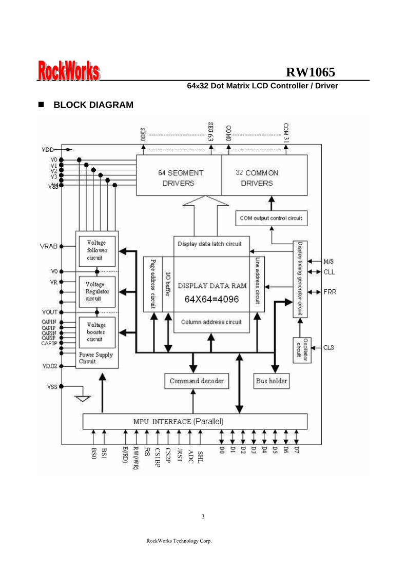
RW1065 64x32 Dot Matrix LCD Controller Driver
RockWorks Technology Corp
3
BLOCK DIAGRAM 31
63
BS0
BS1
AD
C
SHL
V4
RS RST
CS2P
CS1B
P
RW1065 64x32 Dot Matrix LCD Controller Driver
RockWorks Technology Corp
4
PAD ARRANGEMENT
SE
G13
SE
G12
SE
G11
SE
G10
S
EG
9 S
EG
8 S
EG
7 S
EG
6 S
EG
5 S
EG
4 S
EG3
SEG
2 S
EG1
SE
G0
ADC
R
CLL
Vss D0 D1D2 D3 D4 D5 D6 D7 CS1BP CS2P EP RSP RWP VDD RSTP CLSP FRR MSP BS1P BS0P SHLP VDD2 CAP2N CAP2P CAP1P CAP1N CAP3P VOUT V0 VRAB V3 V2 V4 V1 COM0 COM1 COM2 COM3 COM4 COM5 COM6 COM7 COM8
COM9 COM10 COM11 COM12
CO
M13
CO
M14
CO
M15
CO
M16
CO
M17
CO
M18
CO
M19
CO
M20
CO
M21
CO
M22
CO
M23
CO
M24
CO
M25
CO
M27
CO
M26
CO
M28
CO
M29
CO
M30
CO
M31
SEG63 SEG62 SEG61 SEG60 SEG59 SEG58 SEG57 SEG56 SEG55 SEG54 SEG53 SEG52 SEG51 SEG50 SEG49 SEG48 SEG47 SEG46 SEG45 SEG44 SEG43 SEG42 SEG41 SEG40 SEG39 SEG38 SEG37 SEG36 SEG35 SEG34 SEG33 SEG32 SEG31 SEG30 SEG29 SEG28 SEG27 SEG26 SEG25 SEG24 SEG23 SEG22 SEG21 SEG20 SEG19 SEG18 SEG17 SEG16 SEG15 SEG14
123456789101112131415 16 17 18 19
20
21
22232425262728293031323334353637383940414243444546474849505152535455565758596061626364656667
68
69 70 71 72 73 74 75 76 77 78 79 80 81 82 83 84 85 86
87
8889
90919293949596979899100
101
102103
104
105
106107
108109
110
111
112
113
114115
116117
118
119
120
121
122123
124
125
126
127
128129
130
131
132
133
Chip size 4897 um x1902um Pad size 875um x 875um Pad pitch 128um ~ 92um Chip thickness 470 um Substrate connects to VSS
X
Y
C0503
RW1065 64x32 Dot Matrix LCD Controller Driver
RockWorks Technology Corp
5
CHIP LAYOUT
PIN 1
RA
MA
nalog D
igital
RW1065 64x32 Dot Matrix LCD Controller Driver
RockWorks Technology Corp
6
PAD CENTER COORDINATES DUTY=164 duty SHL=0
Pad Pin Name Pin Name Master Slave X Y
Pad No Pin Name X Y Pad
No Master Slave X Y
1 COM13 COM45 -240475 90725 45 SEG38 11025 -90725 89 D2 205225 907252 COM14 COM46 -240475 77975 46 SEG37 20275 -90725 90 D3 19165 907253 COM15 COM47 -240475 66225 47 SEG36 29525 -90725 91 D4 18215 907254 COM16 COM48 -240475 55475 48 SEG35 38775 -90725 92 D5 17265 907255 COM17 COM49 -240475 46275 49 SEG34 48025 -90725 93 D6 16315 907256 COM18 COM50 -240475 37025 50 SEG33 57275 -90725 94 D7 15365 907257 COM19 COM51 -240475 27775 51 SEG32 66525 -90725 95 CS1BP 14415 907258 COM20 COM52 -240475 18525 52 SEG31 75775 -90725 96 CS2P 13465 907259 COM21 COM53 -240475 9275 53 SEG30 85025 -90725 97 EP 12515 9072510 COM22 COM54 -240475 025 54 SEG29 94275 -90725 98 RSP 11565 9072511 COM23 COM55 -240475 -9225 55 SEG28 103525 -90725 99 RWP 10615 9072512 COM24 COM56 -240475 -18475 56 SEG27 112775 -90725 100 VDD 9665 9072513 COM25 COM57 -240475 -27725 57 SEG26 122025 -90725 101 RSTP 8715 9072514 COM26 COM58 -240475 -36975 58 SEG25 131275 -90725 102 CLSP 7765 9072515 COM27 COM59 -240475 -46225 59 SEG24 140525 -90725 103 FRR 6815 9072516 COM28 COM60 -240475 -55475 60 SEG23 149775 -90725 104 MSP 5865 9072517 COM29 COM61 -240475 -66225 61 SEG22 159025 -90725 105 BS1P 4915 9072518 COM30 COM62 -240475 -77975 62 SEG21 168275 -90725 106 BS0P 3965 9072519 COM31 COM63 -240475 -90725 63 SEG20 177525 -90725 107 SHLP 3015 9072520 SEG63 -227725 -90725 64 SEG19 186775 -90725 108 VDD2 2065 9072521 SEG62 -214975 -90725 65 SEG18 196025 -90725 109 CAP2N 1115 9072522 SEG61 -203225 -90725 66 SEG17 205225 -90725 110 CAP2P 165 9072523 SEG60 -192475 -90725 67 SEG16 215975 -90725 111 CAP1P -785 9072524 SEG59 -183225 -90725 68 SEG15 227725 -90725 112 CAP1N -1735 9072525 SEG58 -173975 -90725 69 SEG14 240475 -90725 113 CAP3P -2685 9072526 SEG57 -164725 -90725 70 SEG13 240475 -77975 114 VOUT -3635 9072527 SEG56 -155475 -90725 71 SEG12 240475 -65225 115 V0 -4585 9072528 SEG55 -146225 -90725 72 SEG11 240475 -53475 116 VRAB -5535 9072529 SEG54 -136975 -90725 73 SEG10 240475 -42725 117 V3 -6485 9072530 SEG53 -127725 -90725 74 SEG9 240475 -33475 118 V2 -7435 9072531 SEG52 -118475 -90725 75 SEG8 240475 -24225 119 V4 -8385 9072532 SEG51 -109225 -90725 76 SEG7 240475 -14975 120 V1 -9335 9072533 SEG50 -99975 -90725 77 SEG6 240475 -5725 121 COM0 COM32 -10285 9072534 SEG49 -90725 -90725 78 SEG5 240475 3525 122 COM1 COM33 -11235 9072535 SEG48 -81475 -90725 79 SEG4 240475 12775 123 COM2 COM34 -12185 9072536 SEG47 -72225 -90725 80 SEG3 240475 22025 124 COM3 COM35 -13135 9072537 SEG46 -62975 -90725 81 SEG2 240475 31275 125 COM4 COM36 -14085 9072538 SEG45 -53725 -90725 82 SEG1 240475 40525 126 COM5 COM37 -15035 9072539 SEG44 -44475 -90725 83 SEG0 240475 51275 127 COM6 COM38 -15985 9072540 SEG43 -35225 -90725 84 ADCP 240475 63025 128 COM7 COM39 -16935 9072541 SEG42 -25975 -90725 85 CLL 240475 75775 129 COM8 COM40 -17885 9072542 SEG41 -16725 -90725 86 VSS 240475 90725 130 COM9 COM41 -192475 9072543 SEG40 -7475 -90725 87 D0 227725 90725 131 COM10 COM42 -203225 9072544 SEG39 1775 -90725 88 D1 215975 90725 132 COM11 COM43 -214975 90725 133 COM12 COM44 -227725 90725
RW1065 64x32 Dot Matrix LCD Controller Driver
RockWorks Technology Corp
7
PAD CENTER COORDINATES DUTY=164 duty SHL=1
Pad Pin Name Pin Name Master Slave X Y
Pad No Pin Name X Y Pad
No Master Slave X Y
1 COM50 COM18 -240475 90725 45 SEG38 11025 -90725 89 D2 205225 907252 COM49 COM17 -240475 77975 46 SEG37 20275 -90725 90 D3 19165 907253 COM48 COM16 -240475 66225 47 SEG36 29525 -90725 91 D4 18215 907254 COM47 COM15 -240475 55475 48 SEG35 38775 -90725 92 D5 17265 907255 COM46 COM14 -240475 46275 49 SEG34 48025 -90725 93 D6 16315 907256 COM45 COM13 -240475 37025 50 SEG33 57275 -90725 94 D7 15365 907257 COM44 COM12 -240475 27775 51 SEG32 66525 -90725 95 CS1BP 14415 907258 COM43 COM11 -240475 18525 52 SEG31 75775 -90725 96 CS2P 13465 907259 COM42 COM10 -240475 9275 53 SEG30 85025 -90725 97 EP 12515 9072510 COM41 COM9 -240475 025 54 SEG29 94275 -90725 98 RSP 11565 9072511 COM40 COM8 -240475 -9225 55 SEG28 103525 -90725 99 RWP 10615 9072512 COM39 COM7 -240475 -18475 56 SEG27 112775 -90725 100 VDD 9665 9072513 COM38 COM6 -240475 -27725 57 SEG26 122025 -90725 101 RSTP 8715 9072514 COM37 COM5 -240475 -36975 58 SEG25 131275 -90725 102 CLSP 7765 9072515 COM36 COM4 -240475 -46225 59 SEG24 140525 -90725 103 FRR 6815 9072516 COM35 COM3 -240475 -55475 60 SEG23 149775 -90725 104 MSP 5865 9072517 COM34 COM2 -240475 -66225 61 SEG22 159025 -90725 105 BS1P 4915 9072518 COM33 COM1 -240475 -77975 62 SEG21 168275 -90725 106 BS0P 3965 9072519 COM32 COM0 -240475 -90725 63 SEG20 177525 -90725 107 SHLP 3015 9072520 SEG63 -227725 -90725 64 SEG19 186775 -90725 108 VDD2 2065 9072521 SEG62 -214975 -90725 65 SEG18 196025 -90725 109 CAP2N 1115 9072522 SEG61 -203225 -90725 66 SEG17 205225 -90725 110 CAP2P 165 9072523 SEG60 -192475 -90725 67 SEG16 215975 -90725 111 CAP1P -785 9072524 SEG59 -183225 -90725 68 SEG15 227725 -90725 112 CAP1N -1735 9072525 SEG58 -173975 -90725 69 SEG14 240475 -90725 113 CAP3P -2685 9072526 SEG57 -164725 -90725 70 SEG13 240475 -77975 114 VOUT -3635 9072527 SEG56 -155475 -90725 71 SEG12 240475 -65225 115 V0 -4585 9072528 SEG55 -146225 -90725 72 SEG11 240475 -53475 116 VRAB -5535 9072529 SEG54 -136975 -90725 73 SEG10 240475 -42725 117 V3 -6485 9072530 SEG53 -127725 -90725 74 SEG9 240475 -33475 118 V2 -7435 9072531 SEG52 -118475 -90725 75 SEG8 240475 -24225 119 V4 -8385 9072532 SEG51 -109225 -90725 76 SEG7 240475 -14975 120 V1 -9335 9072533 SEG50 -99975 -90725 77 SEG6 240475 -5725 121 COM63 COM31 -10285 9072534 SEG49 -90725 -90725 78 SEG5 240475 3525 122 COM62 COM30 -11235 9072535 SEG48 -81475 -90725 79 SEG4 240475 12775 123 COM61 COM29 -12185 9072536 SEG47 -72225 -90725 80 SEG3 240475 22025 124 COM60 COM28 -13135 9072537 SEG46 -62975 -90725 81 SEG2 240475 31275 125 COM59 COM27 -14085 9072538 SEG45 -53725 -90725 82 SEG1 240475 40525 126 COM58 COM26 -15035 9072539 SEG44 -44475 -90725 83 SEG0 240475 51275 127 COM57 COM25 -15985 9072540 SEG43 -35225 -90725 84 ADCP 240475 63025 128 COM56 COM24 -16935 9072541 SEG42 -25975 -90725 85 CLL 240475 75775 129 COM55 COM23 -17885 9072542 SEG41 -16725 -90725 86 VSS 240475 90725 130 COM54 COM22 -192475 9072543 SEG40 -7475 -90725 87 D0 227725 90725 131 COM53 COM21 -203225 9072544 SEG39 1775 -90725 88 D1 215975 90725 132 COM52 COM20 -214975 90725 133 COM51 COM19 -227725 90725
RW1065 64x32 Dot Matrix LCD Controller Driver
RockWorks Technology Corp
8
PAD CENTER COORDINATES DUTY=132 duty SHL=0
Pad Pin Name Pin Name Master Slave X Y
Pad No Pin Name X Y Pad
No Master Slave X Y
1 COM13 COM29 -240475 90725 45 SEG38 11025 -90725 89 D2 205225 907252 COM14 COM30 -240475 77975 46 SEG37 20275 -90725 90 D3 19165 907253 COM15 COM31 -240475 66225 47 SEG36 29525 -90725 91 D4 18215 907254 NC NC -240475 55475 48 SEG35 38775 -90725 92 D5 17265 907255 NC NC -240475 46275 49 SEG34 48025 -90725 93 D6 16315 907256 NC NC -240475 37025 50 SEG33 57275 -90725 94 D7 15365 907257 NC NC -240475 27775 51 SEG32 66525 -90725 95 CS1BP 14415 907258 NC NC -240475 18525 52 SEG31 75775 -90725 96 CS2P 13465 907259 NC NC -240475 9275 53 SEG30 85025 -90725 97 EP 12515 9072510 NC NC -240475 025 54 SEG29 94275 -90725 98 RSP 11565 9072511 NC NC -240475 -9225 55 SEG28 103525 -90725 99 RWP 10615 9072512 NC NC -240475 -18475 56 SEG27 112775 -90725 100 VDD 9665 9072513 NC NC -240475 -27725 57 SEG26 122025 -90725 101 RSTP 8715 9072514 NC NC -240475 -36975 58 SEG25 131275 -90725 102 CLSP 7765 9072515 NC NC -240475 -46225 59 SEG24 140525 -90725 103 FRR 6815 9072516 NC NC -240475 -55475 60 SEG23 149775 -90725 104 MSP 5865 9072517 NC NC -240475 -66225 61 SEG22 159025 -90725 105 BS1P 4915 9072518 NC NC -240475 -77975 62 SEG21 168275 -90725 106 BS0P 3965 9072519 NC NC -240475 -90725 63 SEG20 177525 -90725 107 SHLP 3015 9072520 SEG63 -227725 -90725 64 SEG19 186775 -90725 108 VDD2 2065 9072521 SEG62 -214975 -90725 65 SEG18 196025 -90725 109 CAP2N 1115 9072522 SEG61 -203225 -90725 66 SEG17 205225 -90725 110 CAP2P 165 9072523 SEG60 -192475 -90725 67 SEG16 215975 -90725 111 CAP1P -785 9072524 SEG59 -183225 -90725 68 SEG15 227725 -90725 112 CAP1N -1735 9072525 SEG58 -173975 -90725 69 SEG14 240475 -90725 113 CAP3P -2685 9072526 SEG57 -164725 -90725 70 SEG13 240475 -77975 114 VOUT -3635 9072527 SEG56 -155475 -90725 71 SEG12 240475 -65225 115 V0 -4585 9072528 SEG55 -146225 -90725 72 SEG11 240475 -53475 116 VRAB -5535 9072529 SEG54 -136975 -90725 73 SEG10 240475 -42725 117 V3 -6485 9072530 SEG53 -127725 -90725 74 SEG9 240475 -33475 118 V2 -7435 9072531 SEG52 -118475 -90725 75 SEG8 240475 -24225 119 V4 -8385 9072532 SEG51 -109225 -90725 76 SEG7 240475 -14975 120 V1 -9335 9072533 SEG50 -99975 -90725 77 SEG6 240475 -5725 121 COM0 COM16 -10285 9072534 SEG49 -90725 -90725 78 SEG5 240475 3525 122 COM1 COM17 -11235 9072535 SEG48 -81475 -90725 79 SEG4 240475 12775 123 COM2 COM18 -12185 9072536 SEG47 -72225 -90725 80 SEG3 240475 22025 124 COM3 COM19 -13135 9072537 SEG46 -62975 -90725 81 SEG2 240475 31275 125 COM4 COM20 -14085 9072538 SEG45 -53725 -90725 82 SEG1 240475 40525 126 COM5 COM21 -15035 9072539 SEG44 -44475 -90725 83 SEG0 240475 51275 127 COM6 COM22 -15985 9072540 SEG43 -35225 -90725 84 ADCP 240475 63025 128 COM7 COM23 -16935 9072541 SEG42 -25975 -90725 85 CLL 240475 75775 129 COM8 COM24 -17885 9072542 SEG41 -16725 -90725 86 VSS 240475 90725 130 COM9 COM25 -192475 9072543 SEG40 -7475 -90725 87 D0 227725 90725 131 COM10 COM26 -203225 9072544 SEG39 1775 -90725 88 D1 215975 90725 132 COM11 COM27 -214975 90725 133 COM12 COM28 -227725 90725
RW1065 64x32 Dot Matrix LCD Controller Driver
RockWorks Technology Corp
9
PAD CENTER COORDINATES DUTY=132 duty SHL=1
Pad Pin Name Pin Name Master Slave X Y
Pad No Pin Name X Y Pad
No Master Slave X Y
1 COM18 COM2 -240475 90725 45 SEG38 11025 -90725 89 D2 205225 907252 COM17 COM1 -240475 77975 46 SEG37 20275 -90725 90 D3 19165 907253 COM16 COM0 -240475 66225 47 SEG36 29525 -90725 91 D4 18215 907254 NC NC -240475 55475 48 SEG35 38775 -90725 92 D5 17265 907255 NC NC -240475 46275 49 SEG34 48025 -90725 93 D6 16315 907256 NC NC -240475 37025 50 SEG33 57275 -90725 94 D7 15365 907257 NC NC -240475 27775 51 SEG32 66525 -90725 95 CS1BP 14415 907258 NC NC -240475 18525 52 SEG31 75775 -90725 96 CS2P 13465 907259 NC NC -240475 9275 53 SEG30 85025 -90725 97 EP 12515 9072510 NC NC -240475 025 54 SEG29 94275 -90725 98 RSP 11565 9072511 NC NC -240475 -9225 55 SEG28 103525 -90725 99 RWP 10615 9072512 NC NC -240475 -18475 56 SEG27 112775 -90725 100 VDD 9665 9072513 NC NC -240475 -27725 57 SEG26 122025 -90725 101 RSTP 8715 9072514 NC NC -240475 -36975 58 SEG25 131275 -90725 102 CLSP 7765 9072515 NC NC -240475 -46225 59 SEG24 140525 -90725 103 FRR 6815 9072516 NC NC -240475 -55475 60 SEG23 149775 -90725 104 MSP 5865 9072517 NC NC -240475 -66225 61 SEG22 159025 -90725 105 BS1P 4915 9072518 NC NC -240475 -77975 62 SEG21 168275 -90725 106 BS0P 3965 9072519 NC NC -240475 -90725 63 SEG20 177525 -90725 107 SHLP 3015 9072520 SEG63 -227725 -90725 64 SEG19 186775 -90725 108 VDD2 2065 9072521 SEG62 -214975 -90725 65 SEG18 196025 -90725 109 CAP2N 1115 9072522 SEG61 -203225 -90725 66 SEG17 205225 -90725 110 CAP2P 165 9072523 SEG60 -192475 -90725 67 SEG16 215975 -90725 111 CAP1P -785 9072524 SEG59 -183225 -90725 68 SEG15 227725 -90725 112 CAP1N -1735 9072525 SEG58 -173975 -90725 69 SEG14 240475 -90725 113 CAP3P -2685 9072526 SEG57 -164725 -90725 70 SEG13 240475 -77975 114 VOUT -3635 9072527 SEG56 -155475 -90725 71 SEG12 240475 -65225 115 V0 -4585 9072528 SEG55 -146225 -90725 72 SEG11 240475 -53475 116 VRAB -5535 9072529 SEG54 -136975 -90725 73 SEG10 240475 -42725 117 V3 -6485 9072530 SEG53 -127725 -90725 74 SEG9 240475 -33475 118 V2 -7435 9072531 SEG52 -118475 -90725 75 SEG8 240475 -24225 119 V4 -8385 9072532 SEG51 -109225 -90725 76 SEG7 240475 -14975 120 V1 -9335 9072533 SEG50 -99975 -90725 77 SEG6 240475 -5725 121 COM31 COM15 -10285 9072534 SEG49 -90725 -90725 78 SEG5 240475 3525 122 COM30 COM14 -11235 9072535 SEG48 -81475 -90725 79 SEG4 240475 12775 123 COM29 COM13 -12185 9072536 SEG47 -72225 -90725 80 SEG3 240475 22025 124 COM28 COM12 -13135 9072537 SEG46 -62975 -90725 81 SEG2 240475 31275 125 COM27 COM11 -14085 9072538 SEG45 -53725 -90725 82 SEG1 240475 40525 126 COM26 COM10 -15035 9072539 SEG44 -44475 -90725 83 SEG0 240475 51275 127 COM25 COM9 -15985 9072540 SEG43 -35225 -90725 84 ADCP 240475 63025 128 COM24 COM8 -16935 9072541 SEG42 -25975 -90725 85 CLL 240475 75775 129 COM23 COM7 -17885 9072542 SEG41 -16725 -90725 86 VSS 240475 90725 130 COM22 COM6 -192475 9072543 SEG40 -7475 -90725 87 D0 227725 90725 131 COM21 COM5 -203225 9072544 SEG39 1775 -90725 88 D1 215975 90725 132 COM20 COM4 -214975 90725 133 COM19 COM3 -227725 90725
RW1065 64x32 Dot Matrix LCD Controller Driver
RockWorks Technology Corp
10
Pin Description
(1)Power Pins
Name IO Description
VDD - Connected to the +5V 0r +3V dc power Common to the Vcc MPU power pin
VDD2 This is the retevence power supply for the Step-up voltage circuit
VSS - 0V dc pin connected to the system ground
CAP1P~3P CAP1N~2N - Capacitor connector pin for voltage booster
V0~V4 - Multi-level power supplies for LCD driving The voltage determined for each liquid crystal cell is divided by resistance or it is converted in impedance by the op amp and supplied These voltages must satisfy the following V0 ≧ V1 ≧ V2 ≧ V3 ≧V4 ≧ VSS
(2)System Bus Connection Pins Name IO Description
D7 to D0 IO The 8-bit bidirectional data buses to be connected to the 8- or 16- bit standard MCU Data busses
RS I Usually connected to the low-order bit of the MPU address bus and used to identify the data or a command RS=0 D0 to D7 are display control data RS=1 D0 to D7 are display data
CLS I CLS=1 internal oscillator enable CLS=0 external clock operation mode
ADCP I
The pin selects the relationship between display data RAM column addresses and segment drivers ADCP=1 SEG0larrcolumn address 3FHhellipinverted ADCP=0 SEG0larrcolumn address 00Hhellipnormal
SHLP I
The pin selects the com output scan direction SHL=1 Reverse directioncom63rarrcom0 SHL=0 Normal com0rarrcom63 Both master and slave should set identical SHL value
BS1PBS0P I
Select LCD Bias 15 16 18 19 bias BS1P=0 BS0P=0 15 bias BS1P=0 BS0P=1 16 bias BS1P=1 BS0P=0 18 bias BS1P=1 BS0P=1 19 bias
RST ―
I Input low active System reset
CS1BP CS2P I Input When CS1BP = 0 and CS2P = 1 the chip select become active
E I For 68-series MPU Input Active high
Used as an enable clock input of the 68-series MPU
RW I For 68-series MPU Input
Used as an input pin of read control signals (if RW is high) or write control signals signals (if low)
RW1065 64x32 Dot Matrix LCD Controller Driver
RockWorks Technology Corp
11
(3)LCD Driver Circuit Signals
Name IO Description
CLL IO
Inputoutput IO selection
MS = ldquoHrdquo amp CLS = ldquoHrdquo Output MS = ldquoLrdquo amp CLS = ldquoHrdquo Input MS = ldquoXrdquo amp CLS = ldquoLrdquo Input
This is a display data latch signal to count up the line counter and common counterat each signal falling and rising edges
SEGn O Output A single level of V0 V2 V3 and VSS is selected by the combination of display RAM contents and FR signal
COMn O Output The output pin for LCD common (row) driving A single level of V0 V1 V4 and VSS is selected by the combination of common counter output and FR signal The slave LSI has the reverse common output scan sequence than the master LSI
FRR IO
Inputoutput This is the liquid crystal alternating current signal IO terminal lO selection
MS = ldquoHrdquoOutput MS = ldquoLrdquoInput
VRAB I Provides the voltage between V0 and VSS through a resistive voltage divider
MS I
Input The master or slave LSI operation select pin for the RW1065
MS OperatingMode FR CL V0~V4 Power
SupplyInternal
OSC COMMON
Output SEG
output
High Master Output See CLS On On See
CLS COM0-31 SEG0-63
Low Slave Input Input Off Off Off COM32-63
SEG64-127
RW1065 64x32 Dot Matrix LCD Controller Driver
RockWorks Technology Corp
12
DESCRIPTION OF FUNCTIONS
The Parallel Interface (6800 series MPU)
Shared 6800 Series
RS RW Function
1 1 Reads the display data
1 0 Writes the display data
0 1 Status read
0 0 Write control data (command)
The Chip Select The RW1065 Series chips have two chip select terminals CS1
―BP and CS2P
When the chip select is inactive D0 to D7 enter a high impedance state and the RS E and RW inputs are inactive
The Accessing the Display Data RAM and the Internal Registers Data transfer at a higher speed is ensured since the MPU is required to satisfy the cycle time (tCYC) requirement alone in accessing the RW1065 Series Wait time may not be considered And in the RW1065 Series chips each time data is sent from the MPU a type of pipeline process between LSIs is performed through the bus holder attached to the internal data bus Internal data bus For example when the MPU writes data to the display data RAM once the data is stored in the bus holder then it is written to the display data RAM before the next data write cycle Moreover when the MPU reads the display data RAM
the first data read cycle (dummy) stores the read data in the bus holder and then the data is read from the bus holder to the system bus at the next data read cycle There is a certain restriction in the read sequence of the display data RAM Please be advised that data of the specified address is not generated by the read instruction issued immediately after the address setup This data is generated in data read of the second time Thus a dummy read is required whenever the address setup or write cycle operation is conducted This relationship is shown in Figure 2
RW1065 64x32 Dot Matrix LCD Controller Driver
RockWorks Technology Corp
13
E
Fig 2b read timing
E
RW
Fig 2a write timing (RW=rdquoLrdquo)
RS
RS
RW1065 64x32 Dot Matrix LCD Controller Driver
RockWorks Technology Corp
14
Display Data RAM The display data RAM is a RAM that stores the dot data for the display It has a 64 (8 page x 8 bit) x 64 bit structure It is possible to access the desired bit by specifying the page address and the column addressBecause as is shown in Figure 3 the D7 to D0 display data from the MPU corresponds to the liquid crystal display common direction there are few constraints at the time of display data transfer when multiple RW1065 series chips are used
thus and display structures can be created easily and with a high degree of freedom Moreover reading from and writing to the display RAM from the MPU side is performed through the IO buffer which is an independent operation from signal reading for the liquid crystal driver Consequently even if the display data RAM is accessed asynchronously during liquid crystal display it will not cause adverse effects on the display (such as flickering)
0
1
0
0
1
1
0
0
1
0
1
0
0
1
0
1
0
0
1
0
0
0
0
0
0
D0
D1
D2
D3
D4
-
Display data RAM Liquid crystal display
COM0
COM1
COM2
COM3
COM4
-
Figure3
The Page Address Circuit As shown in Figure 4 page address of the display data RAM is specified through the Page Address Set Command The page address must be specified again when changing pages to perform access
The Column Address As is shown in Table 4 the display data RAM column address is specified by the Column Address Set command The specified column address is incremented (+1) with each display data readwrite command This allows the MPU display data to be accessed continuously Moreover the increment of column addresses stops with 3FH Because the column address is independent of the page address when moving for example from page 0 column 3FH to page 1
column 00H it is necessary to respecify both the page address and the column address Furthermore as is shown in Table 4 the ADC command (segment driver direction select command) can be used to reverse the relationship between the display data RAM column address and the segment output Because of this the constraints on the IC layout when the LCD module is assembled can be minimized
Table 4 SEG Output
ADC set SEG0 SEG 63
ADC(D0)=0 0 rarr Column Address rarr 63 ADC(D0)=1 63 larr Column Address larr 0
RW1065 64x32 Dot Matrix LCD Controller Driver
RockWorks Technology Corp
15
Figure 4
Page Address D3 D2 D1 D0
DataSE
G0
SEG
1
SEG
2
SEG
3
SEG
4
SEG
5
SEG
6
SEG
7
SEG
8
helliphelliphelliphellip
SEG
55
SEG
56
SEG
57
SEG
58
SEG
59
SEG
60
SEG
61
SEG
62
SEG
63 SEG
COM
D0 COM0
D1 COM1
D2 COM2
D3 COM3
D4 COM4
D5 COM5
D6 COM6
0 0 0 0
D7
Page 0
COM7
D0 COM8
D1 COM9
D2 COM10
D3 COM11
D4 COM12
D5 COM13
D6 COM14
0 0 0 1
D7
Page 1
COM15
D0 COM16
D1 COM17
D2 COM18
D3 COM19
D4 COM20
D5 COM21
D6 COM22
0 0 1 0
D7
Page 2
COM23
D0 COM24
D1 COM25
D2 COM26
D3 COM27
D4 COM28
D5 COM29
D6 COM30
0 0 1 1
D7
Page 3
COM31
ADC=0 00
01
02
03
04
05
06
07
08
helliphelliphelliphellip 55
56
57
58
59
60
61
62
63
COLUMN ADC=1 63
62
61
60
59
58
57
56
55
helliphelliphelliphellip 08
07
06
05
04
03
02
01
00
RW1065 64x32 Dot Matrix LCD Controller Driver
RockWorks Technology Corp
16
Common Timing Generator Circuit Display Data Latch Circuit Generates common timing signals and FR frame signals from the CL basic clock The 132 or 164 duty (for RW1065) can be selected by the Duty Select command The 132 and 164 duties are provided by two chips consisting of the master and slave chips in the common multi-chip mode
This latch stores one line of display data for use by the LCD driver interface circuitry The output of this latch is controlled by the Display ONOFF
132 duty
164 duty
SHL=0
SHL=1
SHL=0
SHL=1
RW1065 64x32 Dot Matrix LCD Controller Driver
RockWorks Technology Corp
17
Display Timing Generator Circuit
The display timing generator circuit generates the timing signal to the line address circuit and the display data latch circuit using the display clock The display data is latched into the display data latch circuit synchronized with the display clock and is output to the data driver output terminal Reading to the display data liquid crystal driver circuits is completely independent of accesses to the display data RAM by the MPU Consequently even if the display data
RAM is accessed asynchronously during liquid crystal display there is absolutely no adverse effect (such asflickering) on the display Moreover the display timing generator circuit generates the common timing and the liquid crystal alternating current signal (FR) from the display clock It generates a drive wave form using a 2 frame alternating current drive method as is shown in Figure 5 for the liquid crystal drive circuit
Two-frame alternating current drive waveform
Figure 5
When multiple RW1065 Series chips are used the slave chip must be supplied the display timing signals(FR CL) from the master chip
Table 5 shows the status of the FR and CL signals
Table 5 Operating Mode FR CL
Master (MS = ldquoHrdquo) The internal oscillator circuit is enabled (CLS = ldquoHrdquo) The internal oscillator circuit is disabled (CLS = ldquoLrdquo)
Output Output
Output Input
Slave (MS = ldquoLrdquo) The internal oscillator circuit is enabled (CLS = ldquoHrdquo) The internal oscillator circuit is disabled (CLS = ldquoLrdquo)
Input Input
Input Input
RW1065 64x32 Dot Matrix LCD Controller Driver
RockWorks Technology Corp
18
The Liquid Crystal Driver Circuits
These are a 64-channel (RW1065) that generate four voltage levels for driving the liquid crystal The combination of the display data the COM scan signal and the FR signal
produces the liquid crystal drive voltage output Figure 6 shows examples of the SEG and COM output waveform
Figure 6
RW1065 64x32 Dot Matrix LCD Controller Driver
RockWorks Technology Corp
19
The Power Supply Circuit
The power supply circuits are low-power consumption power supply circuits that generate the voltage levels required for the liquid crystal drivers They comprise Booster circuits and voltage follower circuits They are only enabled in master operation The power supply circuits can turn on automatically after power on
Consequently it is possible to make an external power supply and the internal power supply function somewhat in parallel
The Liquid Crystal Voltage Generator Circuit The V0 voltage is produced by a resistive voltage divider outside the IC through VRAB pin and can be produced at the V1 V2 V3 and V4 voltage levels required for liquid crystal driving Moreover when the voltage follower changes the impedance it provides V1 V2 V3 and V4 to the liquid crystal drive circuit 15 bias or 16 bias or 18 bias or 19 bias for RW1065 can be selected by BS0 and BS1 pins V0-Vss maximum voltage is 15V Vout-Vss maximum voltage is 17V If VDD lt 35V it can use the Booster circuit 2x3x4xThe booster voltage can follow the spec condition (Vout-Vss ≦ 17V max voltage) if VDD gt35V only use the 2X3X booster circuit that can ensure the V0-Vss voltage ≦ 15V If use the VDD voltage 5V and 4X booster itrsquos over the spec operation condition To turn on built-in power (boosterfollower) must waiting 200mS to display on for boosterfollower stable Therefore power off must follower ldquopower off sequencerdquo too
Power on Display off
Power off
Power off sequence
Wait time gt200mS
Display on
Power on sequence
RW1065 64x32 Dot Matrix LCD Controller Driver
RockWorks Technology Corp
20
The Reset Circuit
When the RTP input comes to the ldquoLrdquo level these LSIs return to the default state Their default states are as follows 1 Display OFF 2 Display all point on is select to normal 3 Display normalreverse is select to normal 4 164 duty is selected 5 Read modify write OFF 6 Column address set to Address 0 7 Page address set to Page 0 8 Start line set to first line 9 Frame frequency set to default 10 Power save mode released 11 Ext set to ldquo0rdquo When the power is turned on the IC internal state becomes unstable and it is necessary to initialize it using the RSTP terminal After the initialization each input terminal should be controlled normally While RSTP is ldquoLrdquo the oscillator works but the display timing generator stops and the CL FR terminals are fixed to ldquoHrdquo The terminals D0 to D7 are not affected
RW1065 64x32 Dot Matrix LCD Controller Driver
RockWorks Technology Corp
21
TABLE OF RW1065 INSTRUCTIONS
Instruction code Instruction RS RW DB7 DB6 DB5 DB4 DB3 DB2 DB1 DB0 Description
EXT=0 or 1
MODE SET 0 0 0 0 0 0 1 1 0 EXT Set EXT mode
Instruction code Instruction RS RW DB7 DB6 DB5 DB4 DB3 DB2 DB1 DB0 Description
EXT=0 Display ONOFF 0 0 0 0 1 1 1 1 1 D D=0Display OFF
D=1Display ONSet page address 0 0 1 0 1 1 1 P2 P1 P0 Set page address
Set column address 0 0 0 1 Y5 Y4 Y3 Y2 Y1 Y0 Set column
address MSB
Read Status 0 1 BUSY 0 ON OFF RESET 0 0 0 0 Read register
status Write display
data 1 0 Write data Write data into DDRAM
Read display data 1 1 Read data Read data from
DDRAM Set initial
display line register
0 0 1 1 S5 S4 S3 S2 S1 S0 Specify the initial
display line to realize vertical scrolling
Instruction code Instruction RS RW DB7 DB6 DB5 DB4 DB3 DB2 DB1 DB0 Description
EXT=1
NOP 0 0 0 0 0 0 0 0 0 0 no operation
Set modiy-read 0 0 0 0 0 0 1 0 0 0 Set modiy-read
mode
END 0 0 0 0 0 0 1 1 1 0 release modiy-read mode
Set power save mode 0 0 0 0 0 0 0 0 1 PSAVE P=0 normal mode
P=1 sleep mode
0 0 0 0 0 1 0 1 Display
COMMAND (double
command)
0 0 FRSEL
0 0 0 0 REV ALLON DUTY
DUTY=1 64 duty DUTY=0 32 duty ALLON=1display all on ALLON=0display
normal REV=1display reverse REV=0display normal FRSEL=1FR frequency double default FRSEL=0FR frequency default
RW1065 64x32 Dot Matrix LCD Controller Driver
RockWorks Technology Corp
22
Command Description
See the Table of RW1065 instructions The RW1065 series identifies a data bus using a combination of RS E and RW signals As the MPU translates a command in the internal timing only (independent from the external clock) its speed is very high The busy check is usually not required
Display ONOFF
EXT RS RW D7 D6 D5 D4 D3 D2 D1 D0
0 0 0 0 0 1 1 1 1 1 D
This command turns the display on and off D=1 Display ON D=0 Display OFF(default)
Set page Address This command specifies the page address that corresponds to the low address of the display data RAM when it is accessed by the MPU Any bit of the display data RAM can be accessed when its page address and column address are specified The display status is not changed even when the page address is changed
EXT RS RW D7 D6 D5 D4 D3 D2 D1 D0
0 0 0 1 0 1 1 1 A2 A1 A0
This command loads the page address register
A2 A1 A0 Page
0 0 0 0 (default)
0 0 1 1 0 1 0 2 0 1 1 3 1 0 0 4 1 0 1 5 1 1 0 6 1 1 1 7
Page mapping see Figure 4
RW1065 64x32 Dot Matrix LCD Controller Driver
RockWorks Technology Corp
23
Set Column Address This command specifies a column address of the display data RAM When the display data RAM is accessed by the MPU continuously the column address is incremented by I each time it is accessed from the set address Therefore the MPU can access to data continuously The column address stops to be incremented at address 63 and the page address is not changed continuously
EXT RS RW D7 D6 D5 D4 D3 D2 D1 D0
0 0 0 0 1 A5 A4 A3 A2 A1 A0
A5 A4 A3 A2 A1 A0 Column Address0 0 0 0 0 0 0(default) 0 0 0 0 0 1 1
1 1 1 1 1 1 63
Read Status
EXT RS RW D7 D6 D5 D4 D3 D2 D1 D0
0 0 1 BUSY 0 ON OFF RESET 0 0 0 0
The BUSY Flag bit indicates that RW 1065 is operating or no operating
BUSY=1 Operation BUSY=0 Ready
The ONOFF bit indicates the current status of the display It is the inverse of the polarity of the display ONOFF command ONOFF=1 Display OFF ONOFF=0 Display ON The RESET bit indicates whether the driver is executing a hardware or software reset or if it is in normal operating mode RESET=1 Currently executing reset command RESET=0 Normal operation
RW1065 64x32 Dot Matrix LCD Controller Driver
RockWorks Technology Corp
24
Write Display Data
EXT RS RW D7 D6 D5 D4 D3 D2 D1 D0
0 1 0 Write data
Writes 8-bits of data into the display data RAM at a location specified by the contents of the column address and page address registers and then increments the column address register by one
Read Display Data
EXT RS RW D7 D6 D5 D4 D3 D2 D1 D0
0 1 1 Read data
Reads 8-bits of data from the data IO latch updates the contents of the IO latch with display data from the display data RAM location specified by the contents of the column address and page address registers and then increments the column address register After loading a new address into the column address register one dummy read is required before valid data is obtained
Set initial display line register
EXT RS RW D7 D6 D5 D4 D3 D2 D1 D0
0 0 0 1 1 S5 S4 S3 S2 S1 S0
Loads the RAM line address of the initial display line COM 0 into the initial display line register The RAM display data becomes the top line of the LCD screen It is followed by the higher number lines in ascending order corresponding to the duty cycle The screen can be scrolled using this command by incrementing the line address(default value=rdquo00Hrdquo)
RW1065 64x32 Dot Matrix LCD Controller Driver
RockWorks Technology Corp
25
Read-Modify-Write
EXT RS RW D7 D6 D5 D4 D3 D2 D1 D0
1 0 0 0 0 0 0 1 0 0 0
This command defeats column address register auto-increment after data reads The current contents of the column Address register are saved The mode remains active until an End command is received When the End command is entered the column address is returned to the one used during input of Read-Modify-Write Command This function can reduce the load of MPU when data change is repeated as a specific display area Any command other than Data Read or Write can be used in the Read-Modify-Write mode However the Column Address Set command cannot be used
End
EXT RS RW D7 D6 D5 D4 D3 D2 D1 D0
1 0 0 0 0 0 0 1 1 1 0
This command cancels read-modify-write mode and restores the contents of the column address register to their value prior to the receipt of the Read-Modify-Write command
N N+1 N+2 N+3 N+m N
Read -modify-write mode set End
Returm
Column address
Set page address
Set column address
Read-modify-write
Dummy read
Read data
Write data
End
CompletedNo
Yes
RW1065 64x32 Dot Matrix LCD Controller Driver
RockWorks Technology Corp
26
Set power save mode
EXT RS RW D7 D6 D5 D4 D3 D2 D1 D0
1 0 0 0 0 0 0 0 0 1 PSAVE
When power save mode is entered thus greatly reducing power consumption In the power save mode the display data is saved as is the operating mode that was in effect before the power saver mode was initiated and the MPU is still able to access the display data RAM PSAVE=1 Sleep mode PSAVE=0 Normal mode Sleep mode This stops all operations in the LCD display system and as long as there are no accesses from the MPU the consumption current is reduced to a value near the static current The internal modes during sleep mode are as follows 1 The oscillator circuit and the LCD power supply circuit are halted 2 All liquid crystal drive circuits are halted and the segment and common drive outputs output a Vss level
Display command double command
EXT RS RW D7 D6 D5 D4 D3 D2 D1 D0
1 0 0 0 0 0 0 0 1 0 1
1 0 0 FRSEL 0 0 0 0 REV ALLON DUTY
Display NormalReverse set REV=1 Reverse REV=0 Normal(default) Display All Point ONOFF ALLON=1 All display points ON ALLON=0 Normal(default) Select Duty Duty=1 164 duty cycle(default) Duty=0 132 duty cycle FRAME FREQUENCY Select FRSEL=1 Double FRSEL=0 (default)
RW1065 64x32 Dot Matrix LCD Controller Driver
RockWorks Technology Corp
27
Hardware Pin Set
Select ADC by ADC Pin The pin selects the relationship between display data RAM column addresses and segment drivers ADC=1 SEG0larrcolumn address 3FHhellipinverted ADC=0 SEG0larrcolumn address 00Hhellipnormal(default) This command is provided to reduce restrictions on the placement of driver ICs and routing of traces during printed circuit Board design See Figure 4 for a table of segments and column addresses for the two values of D
Select SHL by SHL Pin The pin selects the com output scan direction SHL=1 Reverse directioncom63rarrcom0 SHL=0 Normal com0rarrcom63 Both master and slave should set identical SHL value
Select LCD Bias by BS0 BS1 Pin
BS1 BS0 Bias 0 0 15 bias 0 1 16 bias 1 0 18 bias 1 1 19 bias
RW1065 64x32 Dot Matrix LCD Controller Driver
RockWorks Technology Corp
28
When an External Resistance is Used The liquid crystal power supply voltage V0 is set by adding resistors Rarsquo and Rbrsquo between VDD and VR and between VR and V0 respectively
RW1065
RW1065 64x32 Dot Matrix LCD Controller Driver
RockWorks Technology Corp
29
The set voltage circuits
Using the step-up voltage circuits equipped within the RW1065 chips it is possible to produce a 2X 3X 4X step-up voltage levels 2X step-up
To produce voltage level in the positive direction at the Vout terminal that is 2 times the voltage difference between VSS and VDD2 Please configure set voltage circuits like this Place a 1uF~22uF capacitor between CAP1N and CAP1P Place a 1uF~22uF capacitor between VSS and VOUT Short CAP2P CAP3P and VOUT Leave CAP2N open 3X step-up
To produce voltage level in the positive direction at the Vout terminal that is 3 times the voltage difference between VSS and VDD2 Please configure set voltage circuits like this Place a 1uF~22uF capacitor between CAP1N and CAP1P Place a 1uF~22uF capacitor between VSS and VOUT Place a 1uF~22uF capacitor and 100 ohms resistor between CAP2N and CAP2P Short CAP3P and Vout 4X step-up
To produce voltage level in the positive direction at the Vout terminal that is 4 times the voltage difference between VSS and VDD2 Please configure set voltage circuits like this Place a 1uF~22uF capacitor between CAP1N and CAP1P Place a 1uF~22uF capacitor between VSS and VOUT Place a 1uF~22uF capacitor and 100 ohms resistor between CAP2N and CAP2P Place a 1uF~22uF capacitor and 100 ohms resistor between CAP1N and CAP3P
RW1065 64x32 Dot Matrix LCD Controller Driver
RockWorks Technology Corp
30
ABSOLUTE MAXIMUM RATINGS Characteristics Symbol Value Unit
Power supply voltage VDD -03 to +70 V
LCD driver voltage Vout 0 to +17 V
Input voltage VIN -03 to VDD+03 V
Operating temperature TA -40 to +85
Storage temperature TSTO -55 to +125
DC CHARACTERISTICS
Rating Item Symbol Condition Min Typ Max Unit ApplicablePin
Operating Voltage VDD - 27 30 55 V VDD1
Step up output voltage Vout (Relative to VDD) 0 - 17 V Vout
Voltage follower circuit operating Voltage V0 (Relative to VDD) 0 - 15 V V0
V0 accuracy V0 - 0 - 15 V0
High-level Input Voltage Low-level Input Voltage
VIHC VILC - 07 VDD
Vss - VDD 09 V 2
High-level Output Voltage Low-level Output Voltage
VOHC VOLC
IOH = ndash05 mA IOL = 05 mA
08VDD Vss - VDD
02 VDD V 3
Input leakage current ILI VIN = VDD or VSS -1 - 2 uA 4
Output leakage current ILO - -1 1 uA 5
Liquid Crystal Driver ON Resistance RON
Ta= 25degC(Relative To VDD)
V0 =15 V - 16 20 KΩ SEGn COMn 6
Internal Oscillator fOSC 2286 254 2794 Oscillator
Frequency External Input RECOMMAND fCL
Ta = 25degC 132Duty 2286 254 2794
kHz CL
Internal Oscillator fOSC 45 5 55 Oscillator
Frequency External Input RECOMMAND fCL
Ta = 25degC 164Duty 45 5 55
kHz CL
bullDynamic Consumption Current During Display with the Internal Power Supply OFF Current consumed by total ICs when an external power supply is used
Unless otherwise specified Vss=0V VDD=30V
RW1065 64x32 Dot Matrix LCD Controller Driver
RockWorks Technology Corp
31
Display Pattern OFF
Ta = 25degC Vout=17V Rating Item Symbol Condition Min Typ Max Unit Notes
VDD=30 V V0-Vss=8V - 10 15 RW1065 IDD VDD=50 V V0-Vss=8V - 35 45
microA 7
Display Pattern Checker
Ta = 25degC Vout=17V Rating Item Symbol Condition Min Typ Max Unit Notes
VDD=30 V V0-Vss=8V - 15 20 RW1065 IDD VDD=50 V V0-Vss=8V - 40 50
microA 7
Display Pattern OFF
Ta = 25degC Vout=17V Rating Item Symbol Condition Min Typ Max Unit Notes
VDD=30 V V0-Vss=8V - 15 20 RW1065 IDD VDD=50 V V0-Vss=8V - 40 50
microA 7
Display pattern Checker
Ta = 25degC Vout=17V Rating Item Symbol Condition Min Typ Max Unit Notes
VDD=30 V V0-Vss=8V - 65 80 RW1065 IDD VDD=50 V V0-Vss=8V - 130 150
microA 7
bull Consumption Current at Time of Power Saver Mode VSS = 0 V VDD = 30 V plusmn 10
Rating Item Symbol Condition Min Typ Max Unit Notes
Sleep mode IDD - - 5 10 microA -
References for items market with 1 While a broad range of operating voltages is guaranteed performance cannot be guaranteed if there are sudden fluctuations to the
voltage while the MPU is being accessed 2 The RS D0 to D5 D6 D7 E RW CS1BP CS2P CLS CL FR MS and RST
― terminals
3 The D0 to D7 FR and CL terminals 4 The RS E RW CS1BP CS2P CLS MS and RST
― terminals
5 Applies when the D0 to D5 D6 D7 CL and FR terminals are in a high impedance state 6 These are the resistance values for when a 01 V voltage is applied between the output terminals SEGn or COMn and
the various power supply terminals (V1 V2 V3 and V4) These are specified for the operating voltage (3) range RON = 01 V ∆I (Where ∆I is the current that flows when 01 V is applied while the power supply is ON)
7 It indicates the current consumed on ICs alone when the internal oscillator circuit and display are turned on Does not include the current due to the LCD panel capacity and wiring capacity Applicable only when there is no access from the MPU
RW1065 64x32 Dot Matrix LCD Controller Driver
RockWorks Technology Corp
32
TIMING CHARACTERISTICS
68 Interface
(Ta=-40 to 85 degC) VDD=27 to 45V
Rating VDD=45 to 55V
Rating Item Signal Symbol ConditionMin Max Min Max
Units
Address hold time RS tAH6 0 mdash 0 mdash Address setup time RS tAW6
mdash 0 mdash 0 mdash
ns
System cycle time RS tCYC6 mdash 900 mdash 800 mdash ns Data setup time D0 to D7 tDS6 100 mdash 100 mdash Data hold time D0 to D7 tDH6
mdash 0 mdash 0 mdash
ns
Access time D0 to D7 tACC6 mdash 350 mdash 250
Output disable time D0 to D7 tOH6 CL = 100 pF
mdash 300 mdash 200 ns
Read tEWHR 360 mdash 300 mdash Enable H pulse time
WriteE
tEWHW mdash
360 mdash 300 mdash ns
Read tEWLR 450 mdash 400 mdash Enable L pulse time
WriteE
tEWLW mdash
450 mdash 400 mdash ns
1 All timing is specified using 20 and 80 of VDD as the reference 2 tEWLW and tEWLR are specified as the overlap between CS1BP being ldquoLrdquo (CS2P = ldquoHrdquo) and E
RW1065 64x32 Dot Matrix LCD Controller Driver
RockWorks Technology Corp
33
Reset Timing
Rating Item Signal Symbol Condition
Min Typ Max Units
Reset time mdash tR mdash mdash - 2 micros
Reset ldquoLrdquo pulse width RST tRW mdash 2 - mdash micros
1 When double chip was be used then the duty set command must be set between the tR
RW1065 64x32 Dot Matrix LCD Controller Driver
RockWorks Technology Corp
34
IO PAD CONFIGURATION
RW1065 64x32 Dot Matrix LCD Controller Driver
RockWorks Technology Corp
35
THE MPU INTERFACE (REFERENCE EXAMPLES) The RW1065 Series can be connected to 6800 Series MPUs The display area can be enlarged by using multiple RW1065 Series chips When this is done the chip select signal can be used to select the individual ICs to access
6800 Series MPUs
RW
106
5
RW1065 64x32 Dot Matrix LCD Controller Driver
RockWorks Technology Corp
36
When using external multi-level power supply for LCD driving (REFERENCE EXAMPLE)
Using a resistor divider can provide RW1065 external multi-level power supply for LCD driving
The circuit below shows a resistor divider network which can bias V0 V1 V2 V3 and V4 externally
RW1065 64x32 Dot Matrix LCD Controller Driver
RockWorks Technology Corp
37
bullWhen V0 V1 V2 V3 and V4 are biased by external power supply analog section of RW1065 should be turn off by software during LCD initialization The example in below shows the sequence to turn off analog section when external bias is used Begin of LCD initialization 1 Reset RW1065 2 SET EXT=1 (mode instruction)
RS RW DB7 DB6 DB5 DB4 DB3 DB2 DB1 DB00 0 0 0 0 0 1 1 0 1
3 SET Display Command (double command)
RS RW DB7 DB6 DB5 DB4 DB3 DB2 DB1 DB00 0 0 0 0 0 0 1 0 1 0 0 0 0 1 1 0 0 0 1
4 SET EXT=1 (mode instruction)
RS RW DB7 DB6 DB5 DB4 DB3 DB2 DB1 DB00 0 0 0 0 0 1 1 0 0
End of LCD initialization
bullBecause pins can not set LCD bias when external power supplies are used for LCD driving the bias can be set by an appropriate configuration for a resistor voltage divider networks The example is shown below
VSS
R
R
NR
R
R
RV1
RV2
RV3
RV4
V0
Bias Network Circuit Concept 15 Bias N=1 total = 5R 16 Bias N=2 total =6R 18 Bias N=4 total =8R 19 Bias N=5 total = 9R
RW1065 64x32 Dot Matrix LCD Controller Driver
RockWorks Technology Corp
38
Single chip solution for RW1065 application (REFERENCE EXAMPLE)
For a 64x32 application the duty cycle of LCD panel is 164 and the display duty of RW1065 should be set to 164 The display duty cycle can be selected by the DUTY bit in display command The diagram for 64x32 application is shown below
64 SEGx32COM LCD Panel
164 duty cycle
RW1065 DUTY=1
COM1~33
SEG1~65
RW1065 64x32 Dot Matrix LCD Controller Driver
RockWorks Technology Corp
39
Using an adjustable resistor on the main board to adjust the contrast of liquid crystal display (REFERENCE EXAMPLE)
The schematic shows an adjustable resistor on main board that can adjust voltage level of V0
RW1065 64x32 Dot Matrix LCD Controller Driver
RockWorks Technology Corp
40
Package information (Please pay close attention to the information in this section Do not hesitate to consult with our sale representative if you have any question or concern)
In order to make better bonding yield for RW1065 please follow the tips and recommendations in this section In this section few tips about COB footprint style PCB layout and wire bonding will be discussed
The drawing in below shows the PCB footprint style which we recommend for RW1065 Pads array in
curve shape is easier for Al wire bonding Besides that a real size COB footprint for RW1065 is also shown in below RW1065 COB footprint is also available in powerpcb or protel format for design reference purpose
The ratio is 11
RW1065 64x32 Dot Matrix LCD Controller Driver
RockWorks Technology Corp
41
During COB footprint design there have some tips about footprint that the PCB designer should know The angle between bonding wire and vertical line should less than 45 Otherwise the wire shorts would become very easy to happen at fours corners of the chip
The angle between bonding wire and vertical line could be reduced by expanding the distance between pads array and the chip In addition reducing length in horizon direction of pads array could minimize the angle between bonding wire and vertical line The picture in below will help to illustrate this concept From the experiences COB footprint style affects the bonding yield
Bad Wires are too close to each other
The angle between bonding wire and vertical line is greater than 45
The angle between bonding wire and vertical line is less than 45
Wires are not too close to each other
Reducing length in horizon direction of pads array could minimize the angle between bonding wire and vertical line
The angle between bonding wire and vertical line could be reduced by expanding the distance between pads array and the chip
RW1065 64x32 Dot Matrix LCD Controller Driver
RockWorks Technology Corp
42
If the gap between pads of COB footprint is filled with solder mask coating it is difficult to bond Al wire to
the pads The top solder masks layer that overlap COB footprint area should be removed
Please use 1 mils diameter Al wire for RW1065 wire bonding
1 2 3 4 5 6
A
B
C
D
654321
D
C
B
A
Title
Number RevisionSize
C
Date 29-Aug-2007 Sheet of File D公司資料99seMyDesignddb Drawn By
RW1065
COM131
COM142
COM153
COM164
COM175
COM186
COM197
COM208
COM219
COM2210
COM2311
COM2412
COM2513
COM2614
COM2715
COM2816
COM2917
COM3018
COM3119
SEG
6320
SEG
6221
SEG
6122
SEG
6023
SEG
5924
SEG
5825
SEG
5726
SEG
5627
SEG
5528
SEG
5429
SEG
5330
SEG
5231
SEG
5132
SEG
5033
SEG
4934
SEG
4835
SEG
4736
SEG
4637
SEG
4538
SEG
4439
SEG
4340
SEG
4241
SEG
4142
SEG
4043
SEG
3944
SEG
3845
SEG
3746
SEG
3647
SEG
3548
SEG
3449
SEG
3350
SEG
3251
SEG
3152
SEG
3053
SEG
2954
SEG
2855
SEG
2756
SEG
2657
SEG
2558
SEG
2459
SEG
2360
SEG
2261
SEG
2162
SEG
2063
SEG
1964
SEG
1865
SEG
1766
SEG
1667
SEG
1568
SEG
1469
SEG13 70SEG12 71SEG11 72SEG10 73SEG9 74SEG8 75SEG7 76SEG6 77SEG5 78SEG4 79SEG3 80SEG2 81SEG1 82SEG0 83ADCP 84CLL 85
VSS
86D
087
D1
88D
289
D3
90D
491
D5
92D
693
D7
94C
S1B
P95
CS2
P96
ERD
P97
AO
P(R
S)98
RW
RP
99V
DD
100
RST
P10
1C
LSP
102
FRR
103
MSP
104
BS1
P10
5B
S0P
106
SHLP
107
VD
D2
108
CA
P2N
109
CA
P2P
110
CA
P1P
111
CA
P1N
112
CA
P3P
113
VO
UT
114
V0
115
VR
AB
116
V3
117
V2
118
V4
119
V1
120
CO
M0
121
CO
M1
122
CO
M2
123
CO
M3
124
CO
M4
125
CO
M5
126
CO
M6
127
CO
M7
128
CO
M8
129
CO
M9
130
CO
M10
131
CO
M11
132
CO
M12
133
4897x1902 um
IC1
RW1065
C9CAPR4
100R0603
R30R0603
C8
CAP
C7
CAP
R2
100R0603
R1
0R0603C6 22uf
R50R
R6300R
R7RES1
R8NC R9
100R0603
VDD
R10
NC
R11
100R0603
R12
100R0603
R13
NC
R14
100R0603
R15
NC
VDD
D0
D1
D2
D3
D4
D5
D6
D7
DB[07]
VDDC5
01uf0603
VD
D
CS2
P
123456789
1011121314151617181920
J1
CON20
C1201uf0603
R3951K0603
VDD
CAP Value1UF~22UF
2XPut C6C8 Short R1R3Open R2R4C7C93XPut C6C8C9 R4Short R1Open R2R3C74XOpen R1R3
BS0 BS1 Bias0 0
0 1
1 0
11
15 bias
16 bias
18 bias
19 bias
ADC=0 SEG0lt~column address 00Hnormal(default) ADC=1 SEG0lt~column address 3FHinverted
SHL=0 Normal COM0~gtCOM63(default)SHL=1 Reverse direction COM63~gtCOM0
R16100R0603
LCD PANEL 64X32RockWorks
RW1065 64X32
COM0-31 SEG0-63SHL=0 ADC=0
SHL=1COM31-0
ADC=1SEG63-0
if use single chip for 32 command displaythe display command must select 164 dutyDisplay panel must select 164 duty type
VO
UT
C3P
C1N
C1P
C2P
C2N
VDD2
ADC
SHL
BS0
BS1
CLLADC
V1
V2
V3
V4
VR
AB
V0
VO
UT
C3P
C1N
C1P
C2P
C2N
VD
D2
SHL
BS0
BS1
FRR
RST
P
RW
RS
E CS1
B
CS1
V0RSRWED0D1D2D3D4D5D6D7
RSTPAK
C4
22uf
RBRES1
RA1RES1
C2
22uf
C1
22uf
C3
22uf
C0
22uf
R20
100k0603
R21
100k0603
R17
200K0603
V1
V2
V3
V4 VRAB
V0
V0
OPTION
B
R18
300R0603
RA2RES1
VADJ
R19100R
R23 RES1R22 0R
R24
RES1
R25
0R
VDD
CS1BP
CS2P
CS1
CS1
R26
22R0603
R27
22R0603
C1047uf
C11
01uf
VSS_INVDD_IN
D1DIODE
FGND
鐵框地
VSS
VDD
R28 10RR29 10RR30 10RR31 10RR32 10RR33 10RR34 10RR35 10RR36 10RR37 10RR38 10R
VADJ
1 2 3 4 5 6
A
B
C
D
654321
D
C
B
A
Title
Number RevisionSize
C
Date 29-Aug-2007 Sheet of File D公司資料99seMyDesignddb Drawn By
RW1065
COM131
COM142
COM153
COM164
COM175
COM186
COM197
COM208
COM219
COM2210
COM2311
COM2412
COM2513
COM2614
COM2715
COM2816
COM2917
COM3018
COM3119
SEG
6320
SEG
6221
SEG
6122
SEG
6023
SEG
5924
SEG
5825
SEG
5726
SEG
5627
SEG
5528
SEG
5429
SEG
5330
SEG
5231
SEG
5132
SEG
5033
SEG
4934
SEG
4835
SEG
4736
SEG
4637
SEG
4538
SEG
4439
SEG
4340
SEG
4241
SEG
4142
SEG
4043
SEG
3944
SEG
3845
SEG
3746
SEG
3647
SEG
3548
SEG
3449
SEG
3350
SEG
3251
SEG
3152
SEG
3053
SEG
2954
SEG
2855
SEG
2756
SEG
2657
SEG
2558
SEG
2459
SEG
2360
SEG
2261
SEG
2162
SEG
2063
SEG
1964
SEG
1865
SEG
1766
SEG
1667
SEG
1568
SEG
1469
SEG13 70SEG12 71SEG11 72SEG10 73SEG9 74SEG8 75SEG7 76SEG6 77SEG5 78SEG4 79SEG3 80SEG2 81SEG1 82SEG0 83ADCP 84CLL 85
VSS
86D
087
D1
88D
289
D3
90D
491
D5
92D
693
D7
94C
S1B
P95
CS2
P96
ERD
P97
AO
P(R
S)98
RW
RP
99V
DD
100
RST
P10
1C
LSP
102
FRR
103
MSP
104
BS1
P10
5B
S0P
106
SHLP
107
VD
D2
108
CA
P2N
109
CA
P2P
110
CA
P1P
111
CA
P1N
112
CA
P3P
113
VO
UT
114
V0
115
VR
AB
116
V3
117
V2
118
V4
119
V1
120
CO
M0
121
CO
M1
122
CO
M2
123
CO
M3
124
CO
M4
125
CO
M5
126
CO
M6
127
CO
M7
128
CO
M8
129
CO
M9
130
CO
M10
131
CO
M11
132
CO
M12
133
4897x1902 um
IC1
RW1065 Master
RW1065
COM131
COM142
COM153
COM164
COM175
COM186
COM197
COM208
COM219
COM2210
COM2311
COM2412
COM2513
COM2614
COM2715
COM2816
COM2917
COM3018
COM3119
SEG
6320
SEG
6221
SEG
6122
SEG
6023
SEG
5924
SEG
5825
SEG
5726
SEG
5627
SEG
5528
SEG
5429
SEG
5330
SEG
5231
SEG
5132
SEG
5033
SEG
4934
SEG
4835
SEG
4736
SEG
4637
SEG
4538
SEG
4439
SEG
4340
SEG
4241
SEG
4142
SEG
4043
SEG
3944
SEG
3845
SEG
3746
SEG
3647
SEG
3548
SEG
3449
SEG
3350
SEG
3251
SEG
3152
SEG
3053
SEG
2954
SEG
2855
SEG
2756
SEG
2657
SEG
2558
SEG
2459
SEG
2360
SEG
2261
SEG
2162
SEG
2063
SEG
1964
SEG
1865
SEG
1766
SEG
1667
SEG
1568
SEG
1469
SEG13 70SEG12 71SEG11 72SEG10 73SEG9 74SEG8 75SEG7 76SEG6 77SEG5 78SEG4 79SEG3 80SEG2 81SEG1 82SEG0 83ADCP 84CLL 85
VSS
86D
087
D1
88D
289
D3
90D
491
D5
92D
693
D7
94C
S1B
P95
CS2
P96
ERD
P97
AO
P(R
S)98
RW
RP
99V
DD
100
RST
P10
1C
LSP
102
FRR
103
MSP
104
BS1
P10
5B
S0P
106
SHLP
107
VD
D2
108
CA
P2N
109
CA
P2P
110
CA
P1P
111
CA
P1N
112
CA
P3P
113
VO
UT
114
V0
115
VR
AB
116
V3
117
V2
118
V4
119
V1
120
CO
M0
121
CO
M1
122
CO
M2
123
CO
M3
124
CO
M4
125
CO
M5
126
CO
M6
127
CO
M7
128
CO
M8
129
CO
M9
130
CO
M10
131
CO
M11
132
CO
M12
133
4897x1902 um
IC2
RW1065 Slave
C4
22uf
RBRES1
RA1RES1
C2
22uf
C1
22uf
C3
22uf
C0
22ufC9CAPR4
100R0603
R30R0603
C8
CAP
C7
CAP
R2
100R0603
R1
0R0603C6 22uf
R50R0603
R6300R0603
R7RES1
R8NC R9
100R0603
VDD
R10
NC
R11
100R0603
R12
NC
R13
100R0603
R14
100R0603
R15
NC
R16
100R0603
R17
NC
VDD
D0
D1
D2
D3
D4
D5
D6
D7
D0
D1
D2
D3
D4
D5
D6
D7
DB[07] DB[07]
VDDC10
01uf0603
VD
D
IC1_
CS2
P
VDD
IC2_
CS2
P
VD
D
C11
01uf0603
VSS
VSS
LCD PANEL 128X64
Master COM0-31 Slave COM32-63
Master SEG0-63 Slave SEG64-127
123456789
1011121314151617181920
J1
CON20
Master Slave
CAP Value1UF~22UF
2XPut C6C8 Short R1R3Open R2R4C7C93XPut C6C8C9 R4Short R1Open R2R3C74XOpen R1R3
RockWorksRW1065 128x64
BS0 BS1 Bias0 0
0 1
1 0
11
15 bias
16 bias
18 bias
19 bias
ADC=0 SEG0lt~column address 00Hnormal(default) ADC=1 SEG0lt~column address 3FHinverted
SHL=0 Normal COM0~gtCOM63(default)SHL=1 Reverse direction COM63~gtCOM0Both Master and Slave should set identical SHL value
SHL=0 SHL=0
ADC=0 ADC=0
Slave COM31-0
Slave SEG127-64
SHL=1
ADC=1
SHL=1Master COM63-32
ADC=1Master SEG63-0
R18100R0603
R22
100k0603
R23
100k0603
C501uF0603
R4551K0603
VDD
R19
200K0603
ADC1
ADC2
SHL
BS0
BS1
VDD2
V1
V2
V3
V4 VRAB
V0
V0V
OU
T
C3P
C1N
C1P
C2P
C2N
V1
V2
V3
V4
VR
AB
V0
VO
UT
C3P
C1N
C1P
C2P
C2N
VD
D2
SHL
BS0
BS1
FRR
RST
P
RW
RS
E IC1_
CS1
BP
V1
V2
V3
V4
VR
AB
V0
VO
UT
VD
D2
SHL
BS0
BS1
FRR
RST
P
RW
RS
E IC2_
CS1
BP
CLLADC1
CLLADC2
RSTP
CS1CS2
V0RSRWED0D1D2D3D4D5D6D7
AK
OPTION
R20
300R0603
RA2RES1
VADJ
R21
100R
B
R25 RESR24 0R
R26 RES R27 0RVDD
IC1_CS1BP
IC1_CS2P
CS1
CS1
R28 0R R29 RES
R30 RES R31 0R
IC2_CS1BP
IC2_CS2P
CS2
CS2
R32
22R0603
R33
22R0603
C1001uf
C11
47uf
D1DIODE
FGND
鐵框地
VSS
VDD
R34 10RR35 10RR36 10RR37 10RR38 10RR39 10RR40 10RR41 10RR42 10RR43 10RR44 10R
VSS_INVDD_IN
VADJ
VDD
1 2 3 4 5 6 7 8
A
B
C
D
87654321
D
C
B
A
Title
Number RevisionSize
D
Date 29-Aug-2007 Sheet of File D公司資料 99seMyDesignddb Drawn By
C422uf
RBRES1
RA1RES1
C3
22uf
C2
22uf
C1
22uf
C0
22ufC9CAPR4
100R0603
R30R0603
C8
CAP
C7
CAP
R2
100R0603
R1
0R0603C6 22uf
R220R0603
R23300R0603
R24RES1
R39
NCR40
100 ohm0603
VDD
R41
NC
R42
100 ohm0603
R43
NC
R44
100 ohm0603
R45
NC
R46
100 ohm0603
R47
100 ohm0603
R48
NC
R49
100 ohm0603
R50
NC
VDDCAP Value1UF~22UF
2XPut C6C8 Short R1R3Open R2R4C7C93XPut C6C8C9 R4Short R1Open R2R3C74XOpen R1R3
BS0 BS1 Bias0 0
0 1
1 0
11
15 bias
16 bias
18 bias
19 bias
ADC=0 SEG0lt~column address 00Hnormal(default)
ADC=1 SEG0lt~column address 3FHinverted
SHL=0 Normal COM0~gtCOM63(default)SHL=1 Reverse direction COM63~gtCOM0Both Master and Slave should set identical SHL value
R7
100k0603
R8
100k0603
V1
V2
V3
V4
V0
VRAB
V0
R5
200K
VDD2
VO
UT
C3P
C1N
C1P
C2P
C2N
ADC1
ADC2
ADC3
SHL
BS0
BS1
CS1CS2CS3
V0RSRWED0D1D2D3D4D5D6D7
RSTP
R3851K0603
C5
01uF
VDD
OPTION
R6
300R0603R9100R
RA2RES1
VADJ
RW1065
COM131
COM142
COM153
COM164
COM175
COM186
COM197
COM208
COM219
COM2210
COM2311
COM2412
COM2513
COM2614
COM2715
COM2816
COM2917
COM3018
COM3119
SEG
6320
SEG
6221
SEG
6122
SEG
6023
SEG
5924
SEG
5825
SEG
5726
SEG
5627
SEG
5528
SEG
5429
SEG
5330
SEG
5231
SEG
5132
SEG
5033
SEG
4934
SEG
4835
SEG
4736
SEG
4637
SEG
4538
SEG
4439
SEG
4340
SEG
4241
SEG
4142
SEG
4043
SEG
3944
SEG
3845
SEG
3746
SEG
3647
SEG
3548
SEG
3449
SEG
3350
SEG
3251
SEG
3152
SEG
3053
SEG
2954
SEG
2855
SEG
2756
SEG
2657
SEG
2558
SEG
2459
SEG
2360
SEG
2261
SEG
2162
SEG
2063
SEG
1964
SEG
1865
SEG
1766
SEG
1667
SEG
1568
SEG
1469
SEG13 70SEG12 71SEG11 72SEG10 73SEG9 74SEG8 75SEG7 76SEG6 77SEG5 78SEG4 79SEG3 80SEG2 81SEG1 82SEG0 83ADCP 84CLL 85
VSS
86D
087
D1
88D
289
D3
90D
491
D5
92D
693
D7
94C
S1B
P95
CS2
P96
ERD
P97
AO
P(R
S)98
RW
RP
99V
DD
100
RST
P10
1C
LSP
102
FRR
103
MSP
104
BS1
P10
5B
S0P
106
SHLP
107
VD
D2
108
CA
P2N
109
CA
P2P
110
CA
P1P
111
CA
P1N
112
CA
P3P
113
VO
UT
114
V0
115
VR
AB
116
V3
117
V2
118
V4
119
V1
120
CO
M0
121
CO
M1
122
CO
M2
123
CO
M3
124
CO
M4
125
CO
M5
126
CO
M6
127
CO
M7
128
CO
M8
129
CO
M9
130
CO
M10
131
CO
M11
132
CO
M12
133
4897x1902 um
IC1
RW1065 Master
RW1065
COM131
COM142
COM153
COM164
COM175
COM186
COM197
COM208
COM219
COM2210
COM2311
COM2412
COM2513
COM2614
COM2715
COM2816
COM2917
COM3018
COM3119
SEG
6320
SEG
6221
SEG
6122
SEG
6023
SEG
5924
SEG
5825
SEG
5726
SEG
5627
SEG
5528
SEG
5429
SEG
5330
SEG
5231
SEG
5132
SEG
5033
SEG
4934
SEG
4835
SEG
4736
SEG
4637
SEG
4538
SEG
4439
SEG
4340
SEG
4241
SEG
4142
SEG
4043
SEG
3944
SEG
3845
SEG
3746
SEG
3647
SEG
3548
SEG
3449
SEG
3350
SEG
3251
SEG
3152
SEG
3053
SEG
2954
SEG
2855
SEG
2756
SEG
2657
SEG
2558
SEG
2459
SEG
2360
SEG
2261
SEG
2162
SEG
2063
SEG
1964
SEG
1865
SEG
1766
SEG
1667
SEG
1568
SEG
1469
SEG13 70SEG12 71SEG11 72SEG10 73SEG9 74SEG8 75SEG7 76SEG6 77SEG5 78SEG4 79SEG3 80SEG2 81SEG1 82SEG0 83ADCP 84CLL 85
VSS
86D
087
D1
88D
289
D3
90D
491
D5
92D
693
D7
94C
S1B
P95
CS2
P96
ERD
P97
AO
P(R
S)98
RW
RP
99V
DD
100
RST
P10
1C
LSP
102
FRR
103
MSP
104
BS1
P10
5B
S0P
106
SHLP
107
VD
D2
108
CA
P2N
109
CA
P2P
110
CA
P1P
111
CA
P1N
112
CA
P3P
113
VO
UT
114
V0
115
VR
AB
116
V3
117
V2
118
V4
119
V1
120
CO
M0
121
CO
M1
122
CO
M2
123
CO
M3
124
CO
M4
125
CO
M5
126
CO
M6
127
CO
M7
128
CO
M8
129
CO
M9
130
CO
M10
131
CO
M11
132
CO
M12
133
4897x1902 um
IC2
RW1065 Slave
D0
D1
D2
D3
D4
D5
D6
D7
D0
D1
D2
D3
D4
D5
D6
D7
DB[07] DB[07]
VDDC8
01uf0603
VD
D
VDD
VD
D
C9
01uf0603
VSS
VSS
LCD PANEL 192X64
Master COM0-31 Slave COM32-63
Master SEG0-63 Slave SEG64-127
Master Slave
RockWorksRW1065 192x64
RW1065
COM131
COM142
COM153
COM164
COM175
COM186
COM197
COM208
COM219
COM2210
COM2311
COM2412
COM2513
COM2614
COM2715
COM2816
COM2917
COM3018
COM3119
SEG
6320
SEG
6221
SEG
6122
SEG
6023
SEG
5924
SEG
5825
SEG
5726
SEG
5627
SEG
5528
SEG
5429
SEG
5330
SEG
5231
SEG
5132
SEG
5033
SEG
4934
SEG
4835
SEG
4736
SEG
4637
SEG
4538
SEG
4439
SEG
4340
SEG
4241
SEG
4142
SEG
4043
SEG
3944
SEG
3845
SEG
3746
SEG
3647
SEG
3548
SEG
3449
SEG
3350
SEG
3251
SEG
3152
SEG
3053
SEG
2954
SEG
2855
SEG
2756
SEG
2657
SEG
2558
SEG
2459
SEG
2360
SEG
2261
SEG
2162
SEG
2063
SEG
1964
SEG
1865
SEG
1766
SEG
1667
SEG
1568
SEG
1469
SEG13 70SEG12 71SEG11 72SEG10 73SEG9 74SEG8 75SEG7 76SEG6 77SEG5 78SEG4 79SEG3 80SEG2 81SEG1 82SEG0 83ADCP 84CLL 85
VSS
86D
087
D1
88D
289
D3
90D
491
D5
92D
693
D7
94C
S1B
P95
CS2
P96
ERD
P97
AO
P(R
S)98
RW
RP
99V
DD
100
RST
P10
1C
LSP
102
FRR
103
MSP
104
BS1
P10
5B
S0P
106
SHLP
107
VD
D2
108
CA
P2N
109
CA
P2P
110
CA
P1P
111
CA
P1N
112
CA
P3P
113
VO
UT
114
V0
115
VR
AB
116
V3
117
V2
118
V4
119
V1
120
CO
M0
121
CO
M1
122
CO
M2
123
CO
M3
124
CO
M4
125
CO
M5
126
CO
M6
127
CO
M7
128
CO
M8
129
CO
M9
130
CO
M10
131
CO
M11
132
CO
M12
133
4897x1902 um
IC3
RW1065 Slave
D0
D1
D2
D3
D4
D5
D6
D7
DB[07]
VSS
VSS
VDD
VD
D
C10
01uf0603
Slave SEG128-192
Slave
SHL=0 SHL=0
Master COM63-32SHL=1 SHL=1
Slave COM31-0ADC=0 ADC=0 ADC=0
ADC=1 ADC=1 ADC=1Master SEG63-0 Slave SEG127-64 Slave SEG192-128
R50100R0603
V1
V2
V3
V4
VR
AB
V0
VO
UT
C3P
C1N
C1P
C2P
C2N
VD
D2
SHL
BS0
BS1
FRR
RST
P
RW
RS
E V1
V2
V3
V4
VR
AB
V0
VO
UT
VD
D2
SHL
BS0
BS1
FRR
RST
P
RW
RS
E V1
V2
V3
V4
VR
AB
V0
VO
UT
VD
D2
SHL
BS0
BS1
FRR
RST
P
RW
RS
E
CLL CLL CLLADC1 ADC2 ADC3
R25 10RR26 10RR27 10RR28 10RR29 10RR30 10RR31 10RR32 10RR33 10RR34 10RR35 10R
R36
22R0603
D1DIODE
R3722R0603
C647uf
C701uf
VSS_INVDD_IN
VSS
VDD
VADJ
123456789
101112131415161718192021222324
J1
CON24
AK
FGND
鐵框地
IC1_
CS1
BP
IC1_
CS2
P
IC2_
CS2
PIC
2_C
S1B
P
IC3_
CS1
BP
IC3_
CS2
B
R10 0R R11 RES
R12 RES R13 0RVDD
IC1_CS2B
IC1_CS1BPCS1
CS1
R14 0R R15 RES
R16 RES R17 0RVDDIC2_CS2B
IC2_CS1BPCS2
CS2
R18 0R R19 RES
R20 RES R21 0RVDDIC3_CS2B
IC3_CS1BPCS3
CS3
B
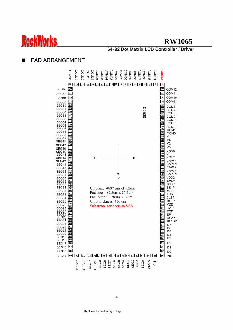
RW1065 64x32 Dot Matrix LCD Controller Driver
RockWorks Technology Corp
4
PAD ARRANGEMENT
SE
G13
SE
G12
SE
G11
SE
G10
S
EG
9 S
EG
8 S
EG
7 S
EG
6 S
EG
5 S
EG
4 S
EG3
SEG
2 S
EG1
SE
G0
ADC
R
CLL
Vss D0 D1D2 D3 D4 D5 D6 D7 CS1BP CS2P EP RSP RWP VDD RSTP CLSP FRR MSP BS1P BS0P SHLP VDD2 CAP2N CAP2P CAP1P CAP1N CAP3P VOUT V0 VRAB V3 V2 V4 V1 COM0 COM1 COM2 COM3 COM4 COM5 COM6 COM7 COM8
COM9 COM10 COM11 COM12
CO
M13
CO
M14
CO
M15
CO
M16
CO
M17
CO
M18
CO
M19
CO
M20
CO
M21
CO
M22
CO
M23
CO
M24
CO
M25
CO
M27
CO
M26
CO
M28
CO
M29
CO
M30
CO
M31
SEG63 SEG62 SEG61 SEG60 SEG59 SEG58 SEG57 SEG56 SEG55 SEG54 SEG53 SEG52 SEG51 SEG50 SEG49 SEG48 SEG47 SEG46 SEG45 SEG44 SEG43 SEG42 SEG41 SEG40 SEG39 SEG38 SEG37 SEG36 SEG35 SEG34 SEG33 SEG32 SEG31 SEG30 SEG29 SEG28 SEG27 SEG26 SEG25 SEG24 SEG23 SEG22 SEG21 SEG20 SEG19 SEG18 SEG17 SEG16 SEG15 SEG14
123456789101112131415 16 17 18 19
20
21
22232425262728293031323334353637383940414243444546474849505152535455565758596061626364656667
68
69 70 71 72 73 74 75 76 77 78 79 80 81 82 83 84 85 86
87
8889
90919293949596979899100
101
102103
104
105
106107
108109
110
111
112
113
114115
116117
118
119
120
121
122123
124
125
126
127
128129
130
131
132
133
Chip size 4897 um x1902um Pad size 875um x 875um Pad pitch 128um ~ 92um Chip thickness 470 um Substrate connects to VSS
X
Y
C0503
RW1065 64x32 Dot Matrix LCD Controller Driver
RockWorks Technology Corp
5
CHIP LAYOUT
PIN 1
RA
MA
nalog D
igital
RW1065 64x32 Dot Matrix LCD Controller Driver
RockWorks Technology Corp
6
PAD CENTER COORDINATES DUTY=164 duty SHL=0
Pad Pin Name Pin Name Master Slave X Y
Pad No Pin Name X Y Pad
No Master Slave X Y
1 COM13 COM45 -240475 90725 45 SEG38 11025 -90725 89 D2 205225 907252 COM14 COM46 -240475 77975 46 SEG37 20275 -90725 90 D3 19165 907253 COM15 COM47 -240475 66225 47 SEG36 29525 -90725 91 D4 18215 907254 COM16 COM48 -240475 55475 48 SEG35 38775 -90725 92 D5 17265 907255 COM17 COM49 -240475 46275 49 SEG34 48025 -90725 93 D6 16315 907256 COM18 COM50 -240475 37025 50 SEG33 57275 -90725 94 D7 15365 907257 COM19 COM51 -240475 27775 51 SEG32 66525 -90725 95 CS1BP 14415 907258 COM20 COM52 -240475 18525 52 SEG31 75775 -90725 96 CS2P 13465 907259 COM21 COM53 -240475 9275 53 SEG30 85025 -90725 97 EP 12515 9072510 COM22 COM54 -240475 025 54 SEG29 94275 -90725 98 RSP 11565 9072511 COM23 COM55 -240475 -9225 55 SEG28 103525 -90725 99 RWP 10615 9072512 COM24 COM56 -240475 -18475 56 SEG27 112775 -90725 100 VDD 9665 9072513 COM25 COM57 -240475 -27725 57 SEG26 122025 -90725 101 RSTP 8715 9072514 COM26 COM58 -240475 -36975 58 SEG25 131275 -90725 102 CLSP 7765 9072515 COM27 COM59 -240475 -46225 59 SEG24 140525 -90725 103 FRR 6815 9072516 COM28 COM60 -240475 -55475 60 SEG23 149775 -90725 104 MSP 5865 9072517 COM29 COM61 -240475 -66225 61 SEG22 159025 -90725 105 BS1P 4915 9072518 COM30 COM62 -240475 -77975 62 SEG21 168275 -90725 106 BS0P 3965 9072519 COM31 COM63 -240475 -90725 63 SEG20 177525 -90725 107 SHLP 3015 9072520 SEG63 -227725 -90725 64 SEG19 186775 -90725 108 VDD2 2065 9072521 SEG62 -214975 -90725 65 SEG18 196025 -90725 109 CAP2N 1115 9072522 SEG61 -203225 -90725 66 SEG17 205225 -90725 110 CAP2P 165 9072523 SEG60 -192475 -90725 67 SEG16 215975 -90725 111 CAP1P -785 9072524 SEG59 -183225 -90725 68 SEG15 227725 -90725 112 CAP1N -1735 9072525 SEG58 -173975 -90725 69 SEG14 240475 -90725 113 CAP3P -2685 9072526 SEG57 -164725 -90725 70 SEG13 240475 -77975 114 VOUT -3635 9072527 SEG56 -155475 -90725 71 SEG12 240475 -65225 115 V0 -4585 9072528 SEG55 -146225 -90725 72 SEG11 240475 -53475 116 VRAB -5535 9072529 SEG54 -136975 -90725 73 SEG10 240475 -42725 117 V3 -6485 9072530 SEG53 -127725 -90725 74 SEG9 240475 -33475 118 V2 -7435 9072531 SEG52 -118475 -90725 75 SEG8 240475 -24225 119 V4 -8385 9072532 SEG51 -109225 -90725 76 SEG7 240475 -14975 120 V1 -9335 9072533 SEG50 -99975 -90725 77 SEG6 240475 -5725 121 COM0 COM32 -10285 9072534 SEG49 -90725 -90725 78 SEG5 240475 3525 122 COM1 COM33 -11235 9072535 SEG48 -81475 -90725 79 SEG4 240475 12775 123 COM2 COM34 -12185 9072536 SEG47 -72225 -90725 80 SEG3 240475 22025 124 COM3 COM35 -13135 9072537 SEG46 -62975 -90725 81 SEG2 240475 31275 125 COM4 COM36 -14085 9072538 SEG45 -53725 -90725 82 SEG1 240475 40525 126 COM5 COM37 -15035 9072539 SEG44 -44475 -90725 83 SEG0 240475 51275 127 COM6 COM38 -15985 9072540 SEG43 -35225 -90725 84 ADCP 240475 63025 128 COM7 COM39 -16935 9072541 SEG42 -25975 -90725 85 CLL 240475 75775 129 COM8 COM40 -17885 9072542 SEG41 -16725 -90725 86 VSS 240475 90725 130 COM9 COM41 -192475 9072543 SEG40 -7475 -90725 87 D0 227725 90725 131 COM10 COM42 -203225 9072544 SEG39 1775 -90725 88 D1 215975 90725 132 COM11 COM43 -214975 90725 133 COM12 COM44 -227725 90725
RW1065 64x32 Dot Matrix LCD Controller Driver
RockWorks Technology Corp
7
PAD CENTER COORDINATES DUTY=164 duty SHL=1
Pad Pin Name Pin Name Master Slave X Y
Pad No Pin Name X Y Pad
No Master Slave X Y
1 COM50 COM18 -240475 90725 45 SEG38 11025 -90725 89 D2 205225 907252 COM49 COM17 -240475 77975 46 SEG37 20275 -90725 90 D3 19165 907253 COM48 COM16 -240475 66225 47 SEG36 29525 -90725 91 D4 18215 907254 COM47 COM15 -240475 55475 48 SEG35 38775 -90725 92 D5 17265 907255 COM46 COM14 -240475 46275 49 SEG34 48025 -90725 93 D6 16315 907256 COM45 COM13 -240475 37025 50 SEG33 57275 -90725 94 D7 15365 907257 COM44 COM12 -240475 27775 51 SEG32 66525 -90725 95 CS1BP 14415 907258 COM43 COM11 -240475 18525 52 SEG31 75775 -90725 96 CS2P 13465 907259 COM42 COM10 -240475 9275 53 SEG30 85025 -90725 97 EP 12515 9072510 COM41 COM9 -240475 025 54 SEG29 94275 -90725 98 RSP 11565 9072511 COM40 COM8 -240475 -9225 55 SEG28 103525 -90725 99 RWP 10615 9072512 COM39 COM7 -240475 -18475 56 SEG27 112775 -90725 100 VDD 9665 9072513 COM38 COM6 -240475 -27725 57 SEG26 122025 -90725 101 RSTP 8715 9072514 COM37 COM5 -240475 -36975 58 SEG25 131275 -90725 102 CLSP 7765 9072515 COM36 COM4 -240475 -46225 59 SEG24 140525 -90725 103 FRR 6815 9072516 COM35 COM3 -240475 -55475 60 SEG23 149775 -90725 104 MSP 5865 9072517 COM34 COM2 -240475 -66225 61 SEG22 159025 -90725 105 BS1P 4915 9072518 COM33 COM1 -240475 -77975 62 SEG21 168275 -90725 106 BS0P 3965 9072519 COM32 COM0 -240475 -90725 63 SEG20 177525 -90725 107 SHLP 3015 9072520 SEG63 -227725 -90725 64 SEG19 186775 -90725 108 VDD2 2065 9072521 SEG62 -214975 -90725 65 SEG18 196025 -90725 109 CAP2N 1115 9072522 SEG61 -203225 -90725 66 SEG17 205225 -90725 110 CAP2P 165 9072523 SEG60 -192475 -90725 67 SEG16 215975 -90725 111 CAP1P -785 9072524 SEG59 -183225 -90725 68 SEG15 227725 -90725 112 CAP1N -1735 9072525 SEG58 -173975 -90725 69 SEG14 240475 -90725 113 CAP3P -2685 9072526 SEG57 -164725 -90725 70 SEG13 240475 -77975 114 VOUT -3635 9072527 SEG56 -155475 -90725 71 SEG12 240475 -65225 115 V0 -4585 9072528 SEG55 -146225 -90725 72 SEG11 240475 -53475 116 VRAB -5535 9072529 SEG54 -136975 -90725 73 SEG10 240475 -42725 117 V3 -6485 9072530 SEG53 -127725 -90725 74 SEG9 240475 -33475 118 V2 -7435 9072531 SEG52 -118475 -90725 75 SEG8 240475 -24225 119 V4 -8385 9072532 SEG51 -109225 -90725 76 SEG7 240475 -14975 120 V1 -9335 9072533 SEG50 -99975 -90725 77 SEG6 240475 -5725 121 COM63 COM31 -10285 9072534 SEG49 -90725 -90725 78 SEG5 240475 3525 122 COM62 COM30 -11235 9072535 SEG48 -81475 -90725 79 SEG4 240475 12775 123 COM61 COM29 -12185 9072536 SEG47 -72225 -90725 80 SEG3 240475 22025 124 COM60 COM28 -13135 9072537 SEG46 -62975 -90725 81 SEG2 240475 31275 125 COM59 COM27 -14085 9072538 SEG45 -53725 -90725 82 SEG1 240475 40525 126 COM58 COM26 -15035 9072539 SEG44 -44475 -90725 83 SEG0 240475 51275 127 COM57 COM25 -15985 9072540 SEG43 -35225 -90725 84 ADCP 240475 63025 128 COM56 COM24 -16935 9072541 SEG42 -25975 -90725 85 CLL 240475 75775 129 COM55 COM23 -17885 9072542 SEG41 -16725 -90725 86 VSS 240475 90725 130 COM54 COM22 -192475 9072543 SEG40 -7475 -90725 87 D0 227725 90725 131 COM53 COM21 -203225 9072544 SEG39 1775 -90725 88 D1 215975 90725 132 COM52 COM20 -214975 90725 133 COM51 COM19 -227725 90725
RW1065 64x32 Dot Matrix LCD Controller Driver
RockWorks Technology Corp
8
PAD CENTER COORDINATES DUTY=132 duty SHL=0
Pad Pin Name Pin Name Master Slave X Y
Pad No Pin Name X Y Pad
No Master Slave X Y
1 COM13 COM29 -240475 90725 45 SEG38 11025 -90725 89 D2 205225 907252 COM14 COM30 -240475 77975 46 SEG37 20275 -90725 90 D3 19165 907253 COM15 COM31 -240475 66225 47 SEG36 29525 -90725 91 D4 18215 907254 NC NC -240475 55475 48 SEG35 38775 -90725 92 D5 17265 907255 NC NC -240475 46275 49 SEG34 48025 -90725 93 D6 16315 907256 NC NC -240475 37025 50 SEG33 57275 -90725 94 D7 15365 907257 NC NC -240475 27775 51 SEG32 66525 -90725 95 CS1BP 14415 907258 NC NC -240475 18525 52 SEG31 75775 -90725 96 CS2P 13465 907259 NC NC -240475 9275 53 SEG30 85025 -90725 97 EP 12515 9072510 NC NC -240475 025 54 SEG29 94275 -90725 98 RSP 11565 9072511 NC NC -240475 -9225 55 SEG28 103525 -90725 99 RWP 10615 9072512 NC NC -240475 -18475 56 SEG27 112775 -90725 100 VDD 9665 9072513 NC NC -240475 -27725 57 SEG26 122025 -90725 101 RSTP 8715 9072514 NC NC -240475 -36975 58 SEG25 131275 -90725 102 CLSP 7765 9072515 NC NC -240475 -46225 59 SEG24 140525 -90725 103 FRR 6815 9072516 NC NC -240475 -55475 60 SEG23 149775 -90725 104 MSP 5865 9072517 NC NC -240475 -66225 61 SEG22 159025 -90725 105 BS1P 4915 9072518 NC NC -240475 -77975 62 SEG21 168275 -90725 106 BS0P 3965 9072519 NC NC -240475 -90725 63 SEG20 177525 -90725 107 SHLP 3015 9072520 SEG63 -227725 -90725 64 SEG19 186775 -90725 108 VDD2 2065 9072521 SEG62 -214975 -90725 65 SEG18 196025 -90725 109 CAP2N 1115 9072522 SEG61 -203225 -90725 66 SEG17 205225 -90725 110 CAP2P 165 9072523 SEG60 -192475 -90725 67 SEG16 215975 -90725 111 CAP1P -785 9072524 SEG59 -183225 -90725 68 SEG15 227725 -90725 112 CAP1N -1735 9072525 SEG58 -173975 -90725 69 SEG14 240475 -90725 113 CAP3P -2685 9072526 SEG57 -164725 -90725 70 SEG13 240475 -77975 114 VOUT -3635 9072527 SEG56 -155475 -90725 71 SEG12 240475 -65225 115 V0 -4585 9072528 SEG55 -146225 -90725 72 SEG11 240475 -53475 116 VRAB -5535 9072529 SEG54 -136975 -90725 73 SEG10 240475 -42725 117 V3 -6485 9072530 SEG53 -127725 -90725 74 SEG9 240475 -33475 118 V2 -7435 9072531 SEG52 -118475 -90725 75 SEG8 240475 -24225 119 V4 -8385 9072532 SEG51 -109225 -90725 76 SEG7 240475 -14975 120 V1 -9335 9072533 SEG50 -99975 -90725 77 SEG6 240475 -5725 121 COM0 COM16 -10285 9072534 SEG49 -90725 -90725 78 SEG5 240475 3525 122 COM1 COM17 -11235 9072535 SEG48 -81475 -90725 79 SEG4 240475 12775 123 COM2 COM18 -12185 9072536 SEG47 -72225 -90725 80 SEG3 240475 22025 124 COM3 COM19 -13135 9072537 SEG46 -62975 -90725 81 SEG2 240475 31275 125 COM4 COM20 -14085 9072538 SEG45 -53725 -90725 82 SEG1 240475 40525 126 COM5 COM21 -15035 9072539 SEG44 -44475 -90725 83 SEG0 240475 51275 127 COM6 COM22 -15985 9072540 SEG43 -35225 -90725 84 ADCP 240475 63025 128 COM7 COM23 -16935 9072541 SEG42 -25975 -90725 85 CLL 240475 75775 129 COM8 COM24 -17885 9072542 SEG41 -16725 -90725 86 VSS 240475 90725 130 COM9 COM25 -192475 9072543 SEG40 -7475 -90725 87 D0 227725 90725 131 COM10 COM26 -203225 9072544 SEG39 1775 -90725 88 D1 215975 90725 132 COM11 COM27 -214975 90725 133 COM12 COM28 -227725 90725
RW1065 64x32 Dot Matrix LCD Controller Driver
RockWorks Technology Corp
9
PAD CENTER COORDINATES DUTY=132 duty SHL=1
Pad Pin Name Pin Name Master Slave X Y
Pad No Pin Name X Y Pad
No Master Slave X Y
1 COM18 COM2 -240475 90725 45 SEG38 11025 -90725 89 D2 205225 907252 COM17 COM1 -240475 77975 46 SEG37 20275 -90725 90 D3 19165 907253 COM16 COM0 -240475 66225 47 SEG36 29525 -90725 91 D4 18215 907254 NC NC -240475 55475 48 SEG35 38775 -90725 92 D5 17265 907255 NC NC -240475 46275 49 SEG34 48025 -90725 93 D6 16315 907256 NC NC -240475 37025 50 SEG33 57275 -90725 94 D7 15365 907257 NC NC -240475 27775 51 SEG32 66525 -90725 95 CS1BP 14415 907258 NC NC -240475 18525 52 SEG31 75775 -90725 96 CS2P 13465 907259 NC NC -240475 9275 53 SEG30 85025 -90725 97 EP 12515 9072510 NC NC -240475 025 54 SEG29 94275 -90725 98 RSP 11565 9072511 NC NC -240475 -9225 55 SEG28 103525 -90725 99 RWP 10615 9072512 NC NC -240475 -18475 56 SEG27 112775 -90725 100 VDD 9665 9072513 NC NC -240475 -27725 57 SEG26 122025 -90725 101 RSTP 8715 9072514 NC NC -240475 -36975 58 SEG25 131275 -90725 102 CLSP 7765 9072515 NC NC -240475 -46225 59 SEG24 140525 -90725 103 FRR 6815 9072516 NC NC -240475 -55475 60 SEG23 149775 -90725 104 MSP 5865 9072517 NC NC -240475 -66225 61 SEG22 159025 -90725 105 BS1P 4915 9072518 NC NC -240475 -77975 62 SEG21 168275 -90725 106 BS0P 3965 9072519 NC NC -240475 -90725 63 SEG20 177525 -90725 107 SHLP 3015 9072520 SEG63 -227725 -90725 64 SEG19 186775 -90725 108 VDD2 2065 9072521 SEG62 -214975 -90725 65 SEG18 196025 -90725 109 CAP2N 1115 9072522 SEG61 -203225 -90725 66 SEG17 205225 -90725 110 CAP2P 165 9072523 SEG60 -192475 -90725 67 SEG16 215975 -90725 111 CAP1P -785 9072524 SEG59 -183225 -90725 68 SEG15 227725 -90725 112 CAP1N -1735 9072525 SEG58 -173975 -90725 69 SEG14 240475 -90725 113 CAP3P -2685 9072526 SEG57 -164725 -90725 70 SEG13 240475 -77975 114 VOUT -3635 9072527 SEG56 -155475 -90725 71 SEG12 240475 -65225 115 V0 -4585 9072528 SEG55 -146225 -90725 72 SEG11 240475 -53475 116 VRAB -5535 9072529 SEG54 -136975 -90725 73 SEG10 240475 -42725 117 V3 -6485 9072530 SEG53 -127725 -90725 74 SEG9 240475 -33475 118 V2 -7435 9072531 SEG52 -118475 -90725 75 SEG8 240475 -24225 119 V4 -8385 9072532 SEG51 -109225 -90725 76 SEG7 240475 -14975 120 V1 -9335 9072533 SEG50 -99975 -90725 77 SEG6 240475 -5725 121 COM31 COM15 -10285 9072534 SEG49 -90725 -90725 78 SEG5 240475 3525 122 COM30 COM14 -11235 9072535 SEG48 -81475 -90725 79 SEG4 240475 12775 123 COM29 COM13 -12185 9072536 SEG47 -72225 -90725 80 SEG3 240475 22025 124 COM28 COM12 -13135 9072537 SEG46 -62975 -90725 81 SEG2 240475 31275 125 COM27 COM11 -14085 9072538 SEG45 -53725 -90725 82 SEG1 240475 40525 126 COM26 COM10 -15035 9072539 SEG44 -44475 -90725 83 SEG0 240475 51275 127 COM25 COM9 -15985 9072540 SEG43 -35225 -90725 84 ADCP 240475 63025 128 COM24 COM8 -16935 9072541 SEG42 -25975 -90725 85 CLL 240475 75775 129 COM23 COM7 -17885 9072542 SEG41 -16725 -90725 86 VSS 240475 90725 130 COM22 COM6 -192475 9072543 SEG40 -7475 -90725 87 D0 227725 90725 131 COM21 COM5 -203225 9072544 SEG39 1775 -90725 88 D1 215975 90725 132 COM20 COM4 -214975 90725 133 COM19 COM3 -227725 90725
RW1065 64x32 Dot Matrix LCD Controller Driver
RockWorks Technology Corp
10
Pin Description
(1)Power Pins
Name IO Description
VDD - Connected to the +5V 0r +3V dc power Common to the Vcc MPU power pin
VDD2 This is the retevence power supply for the Step-up voltage circuit
VSS - 0V dc pin connected to the system ground
CAP1P~3P CAP1N~2N - Capacitor connector pin for voltage booster
V0~V4 - Multi-level power supplies for LCD driving The voltage determined for each liquid crystal cell is divided by resistance or it is converted in impedance by the op amp and supplied These voltages must satisfy the following V0 ≧ V1 ≧ V2 ≧ V3 ≧V4 ≧ VSS
(2)System Bus Connection Pins Name IO Description
D7 to D0 IO The 8-bit bidirectional data buses to be connected to the 8- or 16- bit standard MCU Data busses
RS I Usually connected to the low-order bit of the MPU address bus and used to identify the data or a command RS=0 D0 to D7 are display control data RS=1 D0 to D7 are display data
CLS I CLS=1 internal oscillator enable CLS=0 external clock operation mode
ADCP I
The pin selects the relationship between display data RAM column addresses and segment drivers ADCP=1 SEG0larrcolumn address 3FHhellipinverted ADCP=0 SEG0larrcolumn address 00Hhellipnormal
SHLP I
The pin selects the com output scan direction SHL=1 Reverse directioncom63rarrcom0 SHL=0 Normal com0rarrcom63 Both master and slave should set identical SHL value
BS1PBS0P I
Select LCD Bias 15 16 18 19 bias BS1P=0 BS0P=0 15 bias BS1P=0 BS0P=1 16 bias BS1P=1 BS0P=0 18 bias BS1P=1 BS0P=1 19 bias
RST ―
I Input low active System reset
CS1BP CS2P I Input When CS1BP = 0 and CS2P = 1 the chip select become active
E I For 68-series MPU Input Active high
Used as an enable clock input of the 68-series MPU
RW I For 68-series MPU Input
Used as an input pin of read control signals (if RW is high) or write control signals signals (if low)
RW1065 64x32 Dot Matrix LCD Controller Driver
RockWorks Technology Corp
11
(3)LCD Driver Circuit Signals
Name IO Description
CLL IO
Inputoutput IO selection
MS = ldquoHrdquo amp CLS = ldquoHrdquo Output MS = ldquoLrdquo amp CLS = ldquoHrdquo Input MS = ldquoXrdquo amp CLS = ldquoLrdquo Input
This is a display data latch signal to count up the line counter and common counterat each signal falling and rising edges
SEGn O Output A single level of V0 V2 V3 and VSS is selected by the combination of display RAM contents and FR signal
COMn O Output The output pin for LCD common (row) driving A single level of V0 V1 V4 and VSS is selected by the combination of common counter output and FR signal The slave LSI has the reverse common output scan sequence than the master LSI
FRR IO
Inputoutput This is the liquid crystal alternating current signal IO terminal lO selection
MS = ldquoHrdquoOutput MS = ldquoLrdquoInput
VRAB I Provides the voltage between V0 and VSS through a resistive voltage divider
MS I
Input The master or slave LSI operation select pin for the RW1065
MS OperatingMode FR CL V0~V4 Power
SupplyInternal
OSC COMMON
Output SEG
output
High Master Output See CLS On On See
CLS COM0-31 SEG0-63
Low Slave Input Input Off Off Off COM32-63
SEG64-127
RW1065 64x32 Dot Matrix LCD Controller Driver
RockWorks Technology Corp
12
DESCRIPTION OF FUNCTIONS
The Parallel Interface (6800 series MPU)
Shared 6800 Series
RS RW Function
1 1 Reads the display data
1 0 Writes the display data
0 1 Status read
0 0 Write control data (command)
The Chip Select The RW1065 Series chips have two chip select terminals CS1
―BP and CS2P
When the chip select is inactive D0 to D7 enter a high impedance state and the RS E and RW inputs are inactive
The Accessing the Display Data RAM and the Internal Registers Data transfer at a higher speed is ensured since the MPU is required to satisfy the cycle time (tCYC) requirement alone in accessing the RW1065 Series Wait time may not be considered And in the RW1065 Series chips each time data is sent from the MPU a type of pipeline process between LSIs is performed through the bus holder attached to the internal data bus Internal data bus For example when the MPU writes data to the display data RAM once the data is stored in the bus holder then it is written to the display data RAM before the next data write cycle Moreover when the MPU reads the display data RAM
the first data read cycle (dummy) stores the read data in the bus holder and then the data is read from the bus holder to the system bus at the next data read cycle There is a certain restriction in the read sequence of the display data RAM Please be advised that data of the specified address is not generated by the read instruction issued immediately after the address setup This data is generated in data read of the second time Thus a dummy read is required whenever the address setup or write cycle operation is conducted This relationship is shown in Figure 2
RW1065 64x32 Dot Matrix LCD Controller Driver
RockWorks Technology Corp
13
E
Fig 2b read timing
E
RW
Fig 2a write timing (RW=rdquoLrdquo)
RS
RS
RW1065 64x32 Dot Matrix LCD Controller Driver
RockWorks Technology Corp
14
Display Data RAM The display data RAM is a RAM that stores the dot data for the display It has a 64 (8 page x 8 bit) x 64 bit structure It is possible to access the desired bit by specifying the page address and the column addressBecause as is shown in Figure 3 the D7 to D0 display data from the MPU corresponds to the liquid crystal display common direction there are few constraints at the time of display data transfer when multiple RW1065 series chips are used
thus and display structures can be created easily and with a high degree of freedom Moreover reading from and writing to the display RAM from the MPU side is performed through the IO buffer which is an independent operation from signal reading for the liquid crystal driver Consequently even if the display data RAM is accessed asynchronously during liquid crystal display it will not cause adverse effects on the display (such as flickering)
0
1
0
0
1
1
0
0
1
0
1
0
0
1
0
1
0
0
1
0
0
0
0
0
0
D0
D1
D2
D3
D4
-
Display data RAM Liquid crystal display
COM0
COM1
COM2
COM3
COM4
-
Figure3
The Page Address Circuit As shown in Figure 4 page address of the display data RAM is specified through the Page Address Set Command The page address must be specified again when changing pages to perform access
The Column Address As is shown in Table 4 the display data RAM column address is specified by the Column Address Set command The specified column address is incremented (+1) with each display data readwrite command This allows the MPU display data to be accessed continuously Moreover the increment of column addresses stops with 3FH Because the column address is independent of the page address when moving for example from page 0 column 3FH to page 1
column 00H it is necessary to respecify both the page address and the column address Furthermore as is shown in Table 4 the ADC command (segment driver direction select command) can be used to reverse the relationship between the display data RAM column address and the segment output Because of this the constraints on the IC layout when the LCD module is assembled can be minimized
Table 4 SEG Output
ADC set SEG0 SEG 63
ADC(D0)=0 0 rarr Column Address rarr 63 ADC(D0)=1 63 larr Column Address larr 0
RW1065 64x32 Dot Matrix LCD Controller Driver
RockWorks Technology Corp
15
Figure 4
Page Address D3 D2 D1 D0
DataSE
G0
SEG
1
SEG
2
SEG
3
SEG
4
SEG
5
SEG
6
SEG
7
SEG
8
helliphelliphelliphellip
SEG
55
SEG
56
SEG
57
SEG
58
SEG
59
SEG
60
SEG
61
SEG
62
SEG
63 SEG
COM
D0 COM0
D1 COM1
D2 COM2
D3 COM3
D4 COM4
D5 COM5
D6 COM6
0 0 0 0
D7
Page 0
COM7
D0 COM8
D1 COM9
D2 COM10
D3 COM11
D4 COM12
D5 COM13
D6 COM14
0 0 0 1
D7
Page 1
COM15
D0 COM16
D1 COM17
D2 COM18
D3 COM19
D4 COM20
D5 COM21
D6 COM22
0 0 1 0
D7
Page 2
COM23
D0 COM24
D1 COM25
D2 COM26
D3 COM27
D4 COM28
D5 COM29
D6 COM30
0 0 1 1
D7
Page 3
COM31
ADC=0 00
01
02
03
04
05
06
07
08
helliphelliphelliphellip 55
56
57
58
59
60
61
62
63
COLUMN ADC=1 63
62
61
60
59
58
57
56
55
helliphelliphelliphellip 08
07
06
05
04
03
02
01
00
RW1065 64x32 Dot Matrix LCD Controller Driver
RockWorks Technology Corp
16
Common Timing Generator Circuit Display Data Latch Circuit Generates common timing signals and FR frame signals from the CL basic clock The 132 or 164 duty (for RW1065) can be selected by the Duty Select command The 132 and 164 duties are provided by two chips consisting of the master and slave chips in the common multi-chip mode
This latch stores one line of display data for use by the LCD driver interface circuitry The output of this latch is controlled by the Display ONOFF
132 duty
164 duty
SHL=0
SHL=1
SHL=0
SHL=1
RW1065 64x32 Dot Matrix LCD Controller Driver
RockWorks Technology Corp
17
Display Timing Generator Circuit
The display timing generator circuit generates the timing signal to the line address circuit and the display data latch circuit using the display clock The display data is latched into the display data latch circuit synchronized with the display clock and is output to the data driver output terminal Reading to the display data liquid crystal driver circuits is completely independent of accesses to the display data RAM by the MPU Consequently even if the display data
RAM is accessed asynchronously during liquid crystal display there is absolutely no adverse effect (such asflickering) on the display Moreover the display timing generator circuit generates the common timing and the liquid crystal alternating current signal (FR) from the display clock It generates a drive wave form using a 2 frame alternating current drive method as is shown in Figure 5 for the liquid crystal drive circuit
Two-frame alternating current drive waveform
Figure 5
When multiple RW1065 Series chips are used the slave chip must be supplied the display timing signals(FR CL) from the master chip
Table 5 shows the status of the FR and CL signals
Table 5 Operating Mode FR CL
Master (MS = ldquoHrdquo) The internal oscillator circuit is enabled (CLS = ldquoHrdquo) The internal oscillator circuit is disabled (CLS = ldquoLrdquo)
Output Output
Output Input
Slave (MS = ldquoLrdquo) The internal oscillator circuit is enabled (CLS = ldquoHrdquo) The internal oscillator circuit is disabled (CLS = ldquoLrdquo)
Input Input
Input Input
RW1065 64x32 Dot Matrix LCD Controller Driver
RockWorks Technology Corp
18
The Liquid Crystal Driver Circuits
These are a 64-channel (RW1065) that generate four voltage levels for driving the liquid crystal The combination of the display data the COM scan signal and the FR signal
produces the liquid crystal drive voltage output Figure 6 shows examples of the SEG and COM output waveform
Figure 6
RW1065 64x32 Dot Matrix LCD Controller Driver
RockWorks Technology Corp
19
The Power Supply Circuit
The power supply circuits are low-power consumption power supply circuits that generate the voltage levels required for the liquid crystal drivers They comprise Booster circuits and voltage follower circuits They are only enabled in master operation The power supply circuits can turn on automatically after power on
Consequently it is possible to make an external power supply and the internal power supply function somewhat in parallel
The Liquid Crystal Voltage Generator Circuit The V0 voltage is produced by a resistive voltage divider outside the IC through VRAB pin and can be produced at the V1 V2 V3 and V4 voltage levels required for liquid crystal driving Moreover when the voltage follower changes the impedance it provides V1 V2 V3 and V4 to the liquid crystal drive circuit 15 bias or 16 bias or 18 bias or 19 bias for RW1065 can be selected by BS0 and BS1 pins V0-Vss maximum voltage is 15V Vout-Vss maximum voltage is 17V If VDD lt 35V it can use the Booster circuit 2x3x4xThe booster voltage can follow the spec condition (Vout-Vss ≦ 17V max voltage) if VDD gt35V only use the 2X3X booster circuit that can ensure the V0-Vss voltage ≦ 15V If use the VDD voltage 5V and 4X booster itrsquos over the spec operation condition To turn on built-in power (boosterfollower) must waiting 200mS to display on for boosterfollower stable Therefore power off must follower ldquopower off sequencerdquo too
Power on Display off
Power off
Power off sequence
Wait time gt200mS
Display on
Power on sequence
RW1065 64x32 Dot Matrix LCD Controller Driver
RockWorks Technology Corp
20
The Reset Circuit
When the RTP input comes to the ldquoLrdquo level these LSIs return to the default state Their default states are as follows 1 Display OFF 2 Display all point on is select to normal 3 Display normalreverse is select to normal 4 164 duty is selected 5 Read modify write OFF 6 Column address set to Address 0 7 Page address set to Page 0 8 Start line set to first line 9 Frame frequency set to default 10 Power save mode released 11 Ext set to ldquo0rdquo When the power is turned on the IC internal state becomes unstable and it is necessary to initialize it using the RSTP terminal After the initialization each input terminal should be controlled normally While RSTP is ldquoLrdquo the oscillator works but the display timing generator stops and the CL FR terminals are fixed to ldquoHrdquo The terminals D0 to D7 are not affected
RW1065 64x32 Dot Matrix LCD Controller Driver
RockWorks Technology Corp
21
TABLE OF RW1065 INSTRUCTIONS
Instruction code Instruction RS RW DB7 DB6 DB5 DB4 DB3 DB2 DB1 DB0 Description
EXT=0 or 1
MODE SET 0 0 0 0 0 0 1 1 0 EXT Set EXT mode
Instruction code Instruction RS RW DB7 DB6 DB5 DB4 DB3 DB2 DB1 DB0 Description
EXT=0 Display ONOFF 0 0 0 0 1 1 1 1 1 D D=0Display OFF
D=1Display ONSet page address 0 0 1 0 1 1 1 P2 P1 P0 Set page address
Set column address 0 0 0 1 Y5 Y4 Y3 Y2 Y1 Y0 Set column
address MSB
Read Status 0 1 BUSY 0 ON OFF RESET 0 0 0 0 Read register
status Write display
data 1 0 Write data Write data into DDRAM
Read display data 1 1 Read data Read data from
DDRAM Set initial
display line register
0 0 1 1 S5 S4 S3 S2 S1 S0 Specify the initial
display line to realize vertical scrolling
Instruction code Instruction RS RW DB7 DB6 DB5 DB4 DB3 DB2 DB1 DB0 Description
EXT=1
NOP 0 0 0 0 0 0 0 0 0 0 no operation
Set modiy-read 0 0 0 0 0 0 1 0 0 0 Set modiy-read
mode
END 0 0 0 0 0 0 1 1 1 0 release modiy-read mode
Set power save mode 0 0 0 0 0 0 0 0 1 PSAVE P=0 normal mode
P=1 sleep mode
0 0 0 0 0 1 0 1 Display
COMMAND (double
command)
0 0 FRSEL
0 0 0 0 REV ALLON DUTY
DUTY=1 64 duty DUTY=0 32 duty ALLON=1display all on ALLON=0display
normal REV=1display reverse REV=0display normal FRSEL=1FR frequency double default FRSEL=0FR frequency default
RW1065 64x32 Dot Matrix LCD Controller Driver
RockWorks Technology Corp
22
Command Description
See the Table of RW1065 instructions The RW1065 series identifies a data bus using a combination of RS E and RW signals As the MPU translates a command in the internal timing only (independent from the external clock) its speed is very high The busy check is usually not required
Display ONOFF
EXT RS RW D7 D6 D5 D4 D3 D2 D1 D0
0 0 0 0 0 1 1 1 1 1 D
This command turns the display on and off D=1 Display ON D=0 Display OFF(default)
Set page Address This command specifies the page address that corresponds to the low address of the display data RAM when it is accessed by the MPU Any bit of the display data RAM can be accessed when its page address and column address are specified The display status is not changed even when the page address is changed
EXT RS RW D7 D6 D5 D4 D3 D2 D1 D0
0 0 0 1 0 1 1 1 A2 A1 A0
This command loads the page address register
A2 A1 A0 Page
0 0 0 0 (default)
0 0 1 1 0 1 0 2 0 1 1 3 1 0 0 4 1 0 1 5 1 1 0 6 1 1 1 7
Page mapping see Figure 4
RW1065 64x32 Dot Matrix LCD Controller Driver
RockWorks Technology Corp
23
Set Column Address This command specifies a column address of the display data RAM When the display data RAM is accessed by the MPU continuously the column address is incremented by I each time it is accessed from the set address Therefore the MPU can access to data continuously The column address stops to be incremented at address 63 and the page address is not changed continuously
EXT RS RW D7 D6 D5 D4 D3 D2 D1 D0
0 0 0 0 1 A5 A4 A3 A2 A1 A0
A5 A4 A3 A2 A1 A0 Column Address0 0 0 0 0 0 0(default) 0 0 0 0 0 1 1
1 1 1 1 1 1 63
Read Status
EXT RS RW D7 D6 D5 D4 D3 D2 D1 D0
0 0 1 BUSY 0 ON OFF RESET 0 0 0 0
The BUSY Flag bit indicates that RW 1065 is operating or no operating
BUSY=1 Operation BUSY=0 Ready
The ONOFF bit indicates the current status of the display It is the inverse of the polarity of the display ONOFF command ONOFF=1 Display OFF ONOFF=0 Display ON The RESET bit indicates whether the driver is executing a hardware or software reset or if it is in normal operating mode RESET=1 Currently executing reset command RESET=0 Normal operation
RW1065 64x32 Dot Matrix LCD Controller Driver
RockWorks Technology Corp
24
Write Display Data
EXT RS RW D7 D6 D5 D4 D3 D2 D1 D0
0 1 0 Write data
Writes 8-bits of data into the display data RAM at a location specified by the contents of the column address and page address registers and then increments the column address register by one
Read Display Data
EXT RS RW D7 D6 D5 D4 D3 D2 D1 D0
0 1 1 Read data
Reads 8-bits of data from the data IO latch updates the contents of the IO latch with display data from the display data RAM location specified by the contents of the column address and page address registers and then increments the column address register After loading a new address into the column address register one dummy read is required before valid data is obtained
Set initial display line register
EXT RS RW D7 D6 D5 D4 D3 D2 D1 D0
0 0 0 1 1 S5 S4 S3 S2 S1 S0
Loads the RAM line address of the initial display line COM 0 into the initial display line register The RAM display data becomes the top line of the LCD screen It is followed by the higher number lines in ascending order corresponding to the duty cycle The screen can be scrolled using this command by incrementing the line address(default value=rdquo00Hrdquo)
RW1065 64x32 Dot Matrix LCD Controller Driver
RockWorks Technology Corp
25
Read-Modify-Write
EXT RS RW D7 D6 D5 D4 D3 D2 D1 D0
1 0 0 0 0 0 0 1 0 0 0
This command defeats column address register auto-increment after data reads The current contents of the column Address register are saved The mode remains active until an End command is received When the End command is entered the column address is returned to the one used during input of Read-Modify-Write Command This function can reduce the load of MPU when data change is repeated as a specific display area Any command other than Data Read or Write can be used in the Read-Modify-Write mode However the Column Address Set command cannot be used
End
EXT RS RW D7 D6 D5 D4 D3 D2 D1 D0
1 0 0 0 0 0 0 1 1 1 0
This command cancels read-modify-write mode and restores the contents of the column address register to their value prior to the receipt of the Read-Modify-Write command
N N+1 N+2 N+3 N+m N
Read -modify-write mode set End
Returm
Column address
Set page address
Set column address
Read-modify-write
Dummy read
Read data
Write data
End
CompletedNo
Yes
RW1065 64x32 Dot Matrix LCD Controller Driver
RockWorks Technology Corp
26
Set power save mode
EXT RS RW D7 D6 D5 D4 D3 D2 D1 D0
1 0 0 0 0 0 0 0 0 1 PSAVE
When power save mode is entered thus greatly reducing power consumption In the power save mode the display data is saved as is the operating mode that was in effect before the power saver mode was initiated and the MPU is still able to access the display data RAM PSAVE=1 Sleep mode PSAVE=0 Normal mode Sleep mode This stops all operations in the LCD display system and as long as there are no accesses from the MPU the consumption current is reduced to a value near the static current The internal modes during sleep mode are as follows 1 The oscillator circuit and the LCD power supply circuit are halted 2 All liquid crystal drive circuits are halted and the segment and common drive outputs output a Vss level
Display command double command
EXT RS RW D7 D6 D5 D4 D3 D2 D1 D0
1 0 0 0 0 0 0 0 1 0 1
1 0 0 FRSEL 0 0 0 0 REV ALLON DUTY
Display NormalReverse set REV=1 Reverse REV=0 Normal(default) Display All Point ONOFF ALLON=1 All display points ON ALLON=0 Normal(default) Select Duty Duty=1 164 duty cycle(default) Duty=0 132 duty cycle FRAME FREQUENCY Select FRSEL=1 Double FRSEL=0 (default)
RW1065 64x32 Dot Matrix LCD Controller Driver
RockWorks Technology Corp
27
Hardware Pin Set
Select ADC by ADC Pin The pin selects the relationship between display data RAM column addresses and segment drivers ADC=1 SEG0larrcolumn address 3FHhellipinverted ADC=0 SEG0larrcolumn address 00Hhellipnormal(default) This command is provided to reduce restrictions on the placement of driver ICs and routing of traces during printed circuit Board design See Figure 4 for a table of segments and column addresses for the two values of D
Select SHL by SHL Pin The pin selects the com output scan direction SHL=1 Reverse directioncom63rarrcom0 SHL=0 Normal com0rarrcom63 Both master and slave should set identical SHL value
Select LCD Bias by BS0 BS1 Pin
BS1 BS0 Bias 0 0 15 bias 0 1 16 bias 1 0 18 bias 1 1 19 bias
RW1065 64x32 Dot Matrix LCD Controller Driver
RockWorks Technology Corp
28
When an External Resistance is Used The liquid crystal power supply voltage V0 is set by adding resistors Rarsquo and Rbrsquo between VDD and VR and between VR and V0 respectively
RW1065
RW1065 64x32 Dot Matrix LCD Controller Driver
RockWorks Technology Corp
29
The set voltage circuits
Using the step-up voltage circuits equipped within the RW1065 chips it is possible to produce a 2X 3X 4X step-up voltage levels 2X step-up
To produce voltage level in the positive direction at the Vout terminal that is 2 times the voltage difference between VSS and VDD2 Please configure set voltage circuits like this Place a 1uF~22uF capacitor between CAP1N and CAP1P Place a 1uF~22uF capacitor between VSS and VOUT Short CAP2P CAP3P and VOUT Leave CAP2N open 3X step-up
To produce voltage level in the positive direction at the Vout terminal that is 3 times the voltage difference between VSS and VDD2 Please configure set voltage circuits like this Place a 1uF~22uF capacitor between CAP1N and CAP1P Place a 1uF~22uF capacitor between VSS and VOUT Place a 1uF~22uF capacitor and 100 ohms resistor between CAP2N and CAP2P Short CAP3P and Vout 4X step-up
To produce voltage level in the positive direction at the Vout terminal that is 4 times the voltage difference between VSS and VDD2 Please configure set voltage circuits like this Place a 1uF~22uF capacitor between CAP1N and CAP1P Place a 1uF~22uF capacitor between VSS and VOUT Place a 1uF~22uF capacitor and 100 ohms resistor between CAP2N and CAP2P Place a 1uF~22uF capacitor and 100 ohms resistor between CAP1N and CAP3P
RW1065 64x32 Dot Matrix LCD Controller Driver
RockWorks Technology Corp
30
ABSOLUTE MAXIMUM RATINGS Characteristics Symbol Value Unit
Power supply voltage VDD -03 to +70 V
LCD driver voltage Vout 0 to +17 V
Input voltage VIN -03 to VDD+03 V
Operating temperature TA -40 to +85
Storage temperature TSTO -55 to +125
DC CHARACTERISTICS
Rating Item Symbol Condition Min Typ Max Unit ApplicablePin
Operating Voltage VDD - 27 30 55 V VDD1
Step up output voltage Vout (Relative to VDD) 0 - 17 V Vout
Voltage follower circuit operating Voltage V0 (Relative to VDD) 0 - 15 V V0
V0 accuracy V0 - 0 - 15 V0
High-level Input Voltage Low-level Input Voltage
VIHC VILC - 07 VDD
Vss - VDD 09 V 2
High-level Output Voltage Low-level Output Voltage
VOHC VOLC
IOH = ndash05 mA IOL = 05 mA
08VDD Vss - VDD
02 VDD V 3
Input leakage current ILI VIN = VDD or VSS -1 - 2 uA 4
Output leakage current ILO - -1 1 uA 5
Liquid Crystal Driver ON Resistance RON
Ta= 25degC(Relative To VDD)
V0 =15 V - 16 20 KΩ SEGn COMn 6
Internal Oscillator fOSC 2286 254 2794 Oscillator
Frequency External Input RECOMMAND fCL
Ta = 25degC 132Duty 2286 254 2794
kHz CL
Internal Oscillator fOSC 45 5 55 Oscillator
Frequency External Input RECOMMAND fCL
Ta = 25degC 164Duty 45 5 55
kHz CL
bullDynamic Consumption Current During Display with the Internal Power Supply OFF Current consumed by total ICs when an external power supply is used
Unless otherwise specified Vss=0V VDD=30V
RW1065 64x32 Dot Matrix LCD Controller Driver
RockWorks Technology Corp
31
Display Pattern OFF
Ta = 25degC Vout=17V Rating Item Symbol Condition Min Typ Max Unit Notes
VDD=30 V V0-Vss=8V - 10 15 RW1065 IDD VDD=50 V V0-Vss=8V - 35 45
microA 7
Display Pattern Checker
Ta = 25degC Vout=17V Rating Item Symbol Condition Min Typ Max Unit Notes
VDD=30 V V0-Vss=8V - 15 20 RW1065 IDD VDD=50 V V0-Vss=8V - 40 50
microA 7
Display Pattern OFF
Ta = 25degC Vout=17V Rating Item Symbol Condition Min Typ Max Unit Notes
VDD=30 V V0-Vss=8V - 15 20 RW1065 IDD VDD=50 V V0-Vss=8V - 40 50
microA 7
Display pattern Checker
Ta = 25degC Vout=17V Rating Item Symbol Condition Min Typ Max Unit Notes
VDD=30 V V0-Vss=8V - 65 80 RW1065 IDD VDD=50 V V0-Vss=8V - 130 150
microA 7
bull Consumption Current at Time of Power Saver Mode VSS = 0 V VDD = 30 V plusmn 10
Rating Item Symbol Condition Min Typ Max Unit Notes
Sleep mode IDD - - 5 10 microA -
References for items market with 1 While a broad range of operating voltages is guaranteed performance cannot be guaranteed if there are sudden fluctuations to the
voltage while the MPU is being accessed 2 The RS D0 to D5 D6 D7 E RW CS1BP CS2P CLS CL FR MS and RST
― terminals
3 The D0 to D7 FR and CL terminals 4 The RS E RW CS1BP CS2P CLS MS and RST
― terminals
5 Applies when the D0 to D5 D6 D7 CL and FR terminals are in a high impedance state 6 These are the resistance values for when a 01 V voltage is applied between the output terminals SEGn or COMn and
the various power supply terminals (V1 V2 V3 and V4) These are specified for the operating voltage (3) range RON = 01 V ∆I (Where ∆I is the current that flows when 01 V is applied while the power supply is ON)
7 It indicates the current consumed on ICs alone when the internal oscillator circuit and display are turned on Does not include the current due to the LCD panel capacity and wiring capacity Applicable only when there is no access from the MPU
RW1065 64x32 Dot Matrix LCD Controller Driver
RockWorks Technology Corp
32
TIMING CHARACTERISTICS
68 Interface
(Ta=-40 to 85 degC) VDD=27 to 45V
Rating VDD=45 to 55V
Rating Item Signal Symbol ConditionMin Max Min Max
Units
Address hold time RS tAH6 0 mdash 0 mdash Address setup time RS tAW6
mdash 0 mdash 0 mdash
ns
System cycle time RS tCYC6 mdash 900 mdash 800 mdash ns Data setup time D0 to D7 tDS6 100 mdash 100 mdash Data hold time D0 to D7 tDH6
mdash 0 mdash 0 mdash
ns
Access time D0 to D7 tACC6 mdash 350 mdash 250
Output disable time D0 to D7 tOH6 CL = 100 pF
mdash 300 mdash 200 ns
Read tEWHR 360 mdash 300 mdash Enable H pulse time
WriteE
tEWHW mdash
360 mdash 300 mdash ns
Read tEWLR 450 mdash 400 mdash Enable L pulse time
WriteE
tEWLW mdash
450 mdash 400 mdash ns
1 All timing is specified using 20 and 80 of VDD as the reference 2 tEWLW and tEWLR are specified as the overlap between CS1BP being ldquoLrdquo (CS2P = ldquoHrdquo) and E
RW1065 64x32 Dot Matrix LCD Controller Driver
RockWorks Technology Corp
33
Reset Timing
Rating Item Signal Symbol Condition
Min Typ Max Units
Reset time mdash tR mdash mdash - 2 micros
Reset ldquoLrdquo pulse width RST tRW mdash 2 - mdash micros
1 When double chip was be used then the duty set command must be set between the tR
RW1065 64x32 Dot Matrix LCD Controller Driver
RockWorks Technology Corp
34
IO PAD CONFIGURATION
RW1065 64x32 Dot Matrix LCD Controller Driver
RockWorks Technology Corp
35
THE MPU INTERFACE (REFERENCE EXAMPLES) The RW1065 Series can be connected to 6800 Series MPUs The display area can be enlarged by using multiple RW1065 Series chips When this is done the chip select signal can be used to select the individual ICs to access
6800 Series MPUs
RW
106
5
RW1065 64x32 Dot Matrix LCD Controller Driver
RockWorks Technology Corp
36
When using external multi-level power supply for LCD driving (REFERENCE EXAMPLE)
Using a resistor divider can provide RW1065 external multi-level power supply for LCD driving
The circuit below shows a resistor divider network which can bias V0 V1 V2 V3 and V4 externally
RW1065 64x32 Dot Matrix LCD Controller Driver
RockWorks Technology Corp
37
bullWhen V0 V1 V2 V3 and V4 are biased by external power supply analog section of RW1065 should be turn off by software during LCD initialization The example in below shows the sequence to turn off analog section when external bias is used Begin of LCD initialization 1 Reset RW1065 2 SET EXT=1 (mode instruction)
RS RW DB7 DB6 DB5 DB4 DB3 DB2 DB1 DB00 0 0 0 0 0 1 1 0 1
3 SET Display Command (double command)
RS RW DB7 DB6 DB5 DB4 DB3 DB2 DB1 DB00 0 0 0 0 0 0 1 0 1 0 0 0 0 1 1 0 0 0 1
4 SET EXT=1 (mode instruction)
RS RW DB7 DB6 DB5 DB4 DB3 DB2 DB1 DB00 0 0 0 0 0 1 1 0 0
End of LCD initialization
bullBecause pins can not set LCD bias when external power supplies are used for LCD driving the bias can be set by an appropriate configuration for a resistor voltage divider networks The example is shown below
VSS
R
R
NR
R
R
RV1
RV2
RV3
RV4
V0
Bias Network Circuit Concept 15 Bias N=1 total = 5R 16 Bias N=2 total =6R 18 Bias N=4 total =8R 19 Bias N=5 total = 9R
RW1065 64x32 Dot Matrix LCD Controller Driver
RockWorks Technology Corp
38
Single chip solution for RW1065 application (REFERENCE EXAMPLE)
For a 64x32 application the duty cycle of LCD panel is 164 and the display duty of RW1065 should be set to 164 The display duty cycle can be selected by the DUTY bit in display command The diagram for 64x32 application is shown below
64 SEGx32COM LCD Panel
164 duty cycle
RW1065 DUTY=1
COM1~33
SEG1~65
RW1065 64x32 Dot Matrix LCD Controller Driver
RockWorks Technology Corp
39
Using an adjustable resistor on the main board to adjust the contrast of liquid crystal display (REFERENCE EXAMPLE)
The schematic shows an adjustable resistor on main board that can adjust voltage level of V0
RW1065 64x32 Dot Matrix LCD Controller Driver
RockWorks Technology Corp
40
Package information (Please pay close attention to the information in this section Do not hesitate to consult with our sale representative if you have any question or concern)
In order to make better bonding yield for RW1065 please follow the tips and recommendations in this section In this section few tips about COB footprint style PCB layout and wire bonding will be discussed
The drawing in below shows the PCB footprint style which we recommend for RW1065 Pads array in
curve shape is easier for Al wire bonding Besides that a real size COB footprint for RW1065 is also shown in below RW1065 COB footprint is also available in powerpcb or protel format for design reference purpose
The ratio is 11
RW1065 64x32 Dot Matrix LCD Controller Driver
RockWorks Technology Corp
41
During COB footprint design there have some tips about footprint that the PCB designer should know The angle between bonding wire and vertical line should less than 45 Otherwise the wire shorts would become very easy to happen at fours corners of the chip
The angle between bonding wire and vertical line could be reduced by expanding the distance between pads array and the chip In addition reducing length in horizon direction of pads array could minimize the angle between bonding wire and vertical line The picture in below will help to illustrate this concept From the experiences COB footprint style affects the bonding yield
Bad Wires are too close to each other
The angle between bonding wire and vertical line is greater than 45
The angle between bonding wire and vertical line is less than 45
Wires are not too close to each other
Reducing length in horizon direction of pads array could minimize the angle between bonding wire and vertical line
The angle between bonding wire and vertical line could be reduced by expanding the distance between pads array and the chip
RW1065 64x32 Dot Matrix LCD Controller Driver
RockWorks Technology Corp
42
If the gap between pads of COB footprint is filled with solder mask coating it is difficult to bond Al wire to
the pads The top solder masks layer that overlap COB footprint area should be removed
Please use 1 mils diameter Al wire for RW1065 wire bonding
1 2 3 4 5 6
A
B
C
D
654321
D
C
B
A
Title
Number RevisionSize
C
Date 29-Aug-2007 Sheet of File D公司資料99seMyDesignddb Drawn By
RW1065
COM131
COM142
COM153
COM164
COM175
COM186
COM197
COM208
COM219
COM2210
COM2311
COM2412
COM2513
COM2614
COM2715
COM2816
COM2917
COM3018
COM3119
SEG
6320
SEG
6221
SEG
6122
SEG
6023
SEG
5924
SEG
5825
SEG
5726
SEG
5627
SEG
5528
SEG
5429
SEG
5330
SEG
5231
SEG
5132
SEG
5033
SEG
4934
SEG
4835
SEG
4736
SEG
4637
SEG
4538
SEG
4439
SEG
4340
SEG
4241
SEG
4142
SEG
4043
SEG
3944
SEG
3845
SEG
3746
SEG
3647
SEG
3548
SEG
3449
SEG
3350
SEG
3251
SEG
3152
SEG
3053
SEG
2954
SEG
2855
SEG
2756
SEG
2657
SEG
2558
SEG
2459
SEG
2360
SEG
2261
SEG
2162
SEG
2063
SEG
1964
SEG
1865
SEG
1766
SEG
1667
SEG
1568
SEG
1469
SEG13 70SEG12 71SEG11 72SEG10 73SEG9 74SEG8 75SEG7 76SEG6 77SEG5 78SEG4 79SEG3 80SEG2 81SEG1 82SEG0 83ADCP 84CLL 85
VSS
86D
087
D1
88D
289
D3
90D
491
D5
92D
693
D7
94C
S1B
P95
CS2
P96
ERD
P97
AO
P(R
S)98
RW
RP
99V
DD
100
RST
P10
1C
LSP
102
FRR
103
MSP
104
BS1
P10
5B
S0P
106
SHLP
107
VD
D2
108
CA
P2N
109
CA
P2P
110
CA
P1P
111
CA
P1N
112
CA
P3P
113
VO
UT
114
V0
115
VR
AB
116
V3
117
V2
118
V4
119
V1
120
CO
M0
121
CO
M1
122
CO
M2
123
CO
M3
124
CO
M4
125
CO
M5
126
CO
M6
127
CO
M7
128
CO
M8
129
CO
M9
130
CO
M10
131
CO
M11
132
CO
M12
133
4897x1902 um
IC1
RW1065
C9CAPR4
100R0603
R30R0603
C8
CAP
C7
CAP
R2
100R0603
R1
0R0603C6 22uf
R50R
R6300R
R7RES1
R8NC R9
100R0603
VDD
R10
NC
R11
100R0603
R12
100R0603
R13
NC
R14
100R0603
R15
NC
VDD
D0
D1
D2
D3
D4
D5
D6
D7
DB[07]
VDDC5
01uf0603
VD
D
CS2
P
123456789
1011121314151617181920
J1
CON20
C1201uf0603
R3951K0603
VDD
CAP Value1UF~22UF
2XPut C6C8 Short R1R3Open R2R4C7C93XPut C6C8C9 R4Short R1Open R2R3C74XOpen R1R3
BS0 BS1 Bias0 0
0 1
1 0
11
15 bias
16 bias
18 bias
19 bias
ADC=0 SEG0lt~column address 00Hnormal(default) ADC=1 SEG0lt~column address 3FHinverted
SHL=0 Normal COM0~gtCOM63(default)SHL=1 Reverse direction COM63~gtCOM0
R16100R0603
LCD PANEL 64X32RockWorks
RW1065 64X32
COM0-31 SEG0-63SHL=0 ADC=0
SHL=1COM31-0
ADC=1SEG63-0
if use single chip for 32 command displaythe display command must select 164 dutyDisplay panel must select 164 duty type
VO
UT
C3P
C1N
C1P
C2P
C2N
VDD2
ADC
SHL
BS0
BS1
CLLADC
V1
V2
V3
V4
VR
AB
V0
VO
UT
C3P
C1N
C1P
C2P
C2N
VD
D2
SHL
BS0
BS1
FRR
RST
P
RW
RS
E CS1
B
CS1
V0RSRWED0D1D2D3D4D5D6D7
RSTPAK
C4
22uf
RBRES1
RA1RES1
C2
22uf
C1
22uf
C3
22uf
C0
22uf
R20
100k0603
R21
100k0603
R17
200K0603
V1
V2
V3
V4 VRAB
V0
V0
OPTION
B
R18
300R0603
RA2RES1
VADJ
R19100R
R23 RES1R22 0R
R24
RES1
R25
0R
VDD
CS1BP
CS2P
CS1
CS1
R26
22R0603
R27
22R0603
C1047uf
C11
01uf
VSS_INVDD_IN
D1DIODE
FGND
鐵框地
VSS
VDD
R28 10RR29 10RR30 10RR31 10RR32 10RR33 10RR34 10RR35 10RR36 10RR37 10RR38 10R
VADJ
1 2 3 4 5 6
A
B
C
D
654321
D
C
B
A
Title
Number RevisionSize
C
Date 29-Aug-2007 Sheet of File D公司資料99seMyDesignddb Drawn By
RW1065
COM131
COM142
COM153
COM164
COM175
COM186
COM197
COM208
COM219
COM2210
COM2311
COM2412
COM2513
COM2614
COM2715
COM2816
COM2917
COM3018
COM3119
SEG
6320
SEG
6221
SEG
6122
SEG
6023
SEG
5924
SEG
5825
SEG
5726
SEG
5627
SEG
5528
SEG
5429
SEG
5330
SEG
5231
SEG
5132
SEG
5033
SEG
4934
SEG
4835
SEG
4736
SEG
4637
SEG
4538
SEG
4439
SEG
4340
SEG
4241
SEG
4142
SEG
4043
SEG
3944
SEG
3845
SEG
3746
SEG
3647
SEG
3548
SEG
3449
SEG
3350
SEG
3251
SEG
3152
SEG
3053
SEG
2954
SEG
2855
SEG
2756
SEG
2657
SEG
2558
SEG
2459
SEG
2360
SEG
2261
SEG
2162
SEG
2063
SEG
1964
SEG
1865
SEG
1766
SEG
1667
SEG
1568
SEG
1469
SEG13 70SEG12 71SEG11 72SEG10 73SEG9 74SEG8 75SEG7 76SEG6 77SEG5 78SEG4 79SEG3 80SEG2 81SEG1 82SEG0 83ADCP 84CLL 85
VSS
86D
087
D1
88D
289
D3
90D
491
D5
92D
693
D7
94C
S1B
P95
CS2
P96
ERD
P97
AO
P(R
S)98
RW
RP
99V
DD
100
RST
P10
1C
LSP
102
FRR
103
MSP
104
BS1
P10
5B
S0P
106
SHLP
107
VD
D2
108
CA
P2N
109
CA
P2P
110
CA
P1P
111
CA
P1N
112
CA
P3P
113
VO
UT
114
V0
115
VR
AB
116
V3
117
V2
118
V4
119
V1
120
CO
M0
121
CO
M1
122
CO
M2
123
CO
M3
124
CO
M4
125
CO
M5
126
CO
M6
127
CO
M7
128
CO
M8
129
CO
M9
130
CO
M10
131
CO
M11
132
CO
M12
133
4897x1902 um
IC1
RW1065 Master
RW1065
COM131
COM142
COM153
COM164
COM175
COM186
COM197
COM208
COM219
COM2210
COM2311
COM2412
COM2513
COM2614
COM2715
COM2816
COM2917
COM3018
COM3119
SEG
6320
SEG
6221
SEG
6122
SEG
6023
SEG
5924
SEG
5825
SEG
5726
SEG
5627
SEG
5528
SEG
5429
SEG
5330
SEG
5231
SEG
5132
SEG
5033
SEG
4934
SEG
4835
SEG
4736
SEG
4637
SEG
4538
SEG
4439
SEG
4340
SEG
4241
SEG
4142
SEG
4043
SEG
3944
SEG
3845
SEG
3746
SEG
3647
SEG
3548
SEG
3449
SEG
3350
SEG
3251
SEG
3152
SEG
3053
SEG
2954
SEG
2855
SEG
2756
SEG
2657
SEG
2558
SEG
2459
SEG
2360
SEG
2261
SEG
2162
SEG
2063
SEG
1964
SEG
1865
SEG
1766
SEG
1667
SEG
1568
SEG
1469
SEG13 70SEG12 71SEG11 72SEG10 73SEG9 74SEG8 75SEG7 76SEG6 77SEG5 78SEG4 79SEG3 80SEG2 81SEG1 82SEG0 83ADCP 84CLL 85
VSS
86D
087
D1
88D
289
D3
90D
491
D5
92D
693
D7
94C
S1B
P95
CS2
P96
ERD
P97
AO
P(R
S)98
RW
RP
99V
DD
100
RST
P10
1C
LSP
102
FRR
103
MSP
104
BS1
P10
5B
S0P
106
SHLP
107
VD
D2
108
CA
P2N
109
CA
P2P
110
CA
P1P
111
CA
P1N
112
CA
P3P
113
VO
UT
114
V0
115
VR
AB
116
V3
117
V2
118
V4
119
V1
120
CO
M0
121
CO
M1
122
CO
M2
123
CO
M3
124
CO
M4
125
CO
M5
126
CO
M6
127
CO
M7
128
CO
M8
129
CO
M9
130
CO
M10
131
CO
M11
132
CO
M12
133
4897x1902 um
IC2
RW1065 Slave
C4
22uf
RBRES1
RA1RES1
C2
22uf
C1
22uf
C3
22uf
C0
22ufC9CAPR4
100R0603
R30R0603
C8
CAP
C7
CAP
R2
100R0603
R1
0R0603C6 22uf
R50R0603
R6300R0603
R7RES1
R8NC R9
100R0603
VDD
R10
NC
R11
100R0603
R12
NC
R13
100R0603
R14
100R0603
R15
NC
R16
100R0603
R17
NC
VDD
D0
D1
D2
D3
D4
D5
D6
D7
D0
D1
D2
D3
D4
D5
D6
D7
DB[07] DB[07]
VDDC10
01uf0603
VD
D
IC1_
CS2
P
VDD
IC2_
CS2
P
VD
D
C11
01uf0603
VSS
VSS
LCD PANEL 128X64
Master COM0-31 Slave COM32-63
Master SEG0-63 Slave SEG64-127
123456789
1011121314151617181920
J1
CON20
Master Slave
CAP Value1UF~22UF
2XPut C6C8 Short R1R3Open R2R4C7C93XPut C6C8C9 R4Short R1Open R2R3C74XOpen R1R3
RockWorksRW1065 128x64
BS0 BS1 Bias0 0
0 1
1 0
11
15 bias
16 bias
18 bias
19 bias
ADC=0 SEG0lt~column address 00Hnormal(default) ADC=1 SEG0lt~column address 3FHinverted
SHL=0 Normal COM0~gtCOM63(default)SHL=1 Reverse direction COM63~gtCOM0Both Master and Slave should set identical SHL value
SHL=0 SHL=0
ADC=0 ADC=0
Slave COM31-0
Slave SEG127-64
SHL=1
ADC=1
SHL=1Master COM63-32
ADC=1Master SEG63-0
R18100R0603
R22
100k0603
R23
100k0603
C501uF0603
R4551K0603
VDD
R19
200K0603
ADC1
ADC2
SHL
BS0
BS1
VDD2
V1
V2
V3
V4 VRAB
V0
V0V
OU
T
C3P
C1N
C1P
C2P
C2N
V1
V2
V3
V4
VR
AB
V0
VO
UT
C3P
C1N
C1P
C2P
C2N
VD
D2
SHL
BS0
BS1
FRR
RST
P
RW
RS
E IC1_
CS1
BP
V1
V2
V3
V4
VR
AB
V0
VO
UT
VD
D2
SHL
BS0
BS1
FRR
RST
P
RW
RS
E IC2_
CS1
BP
CLLADC1
CLLADC2
RSTP
CS1CS2
V0RSRWED0D1D2D3D4D5D6D7
AK
OPTION
R20
300R0603
RA2RES1
VADJ
R21
100R
B
R25 RESR24 0R
R26 RES R27 0RVDD
IC1_CS1BP
IC1_CS2P
CS1
CS1
R28 0R R29 RES
R30 RES R31 0R
IC2_CS1BP
IC2_CS2P
CS2
CS2
R32
22R0603
R33
22R0603
C1001uf
C11
47uf
D1DIODE
FGND
鐵框地
VSS
VDD
R34 10RR35 10RR36 10RR37 10RR38 10RR39 10RR40 10RR41 10RR42 10RR43 10RR44 10R
VSS_INVDD_IN
VADJ
VDD
1 2 3 4 5 6 7 8
A
B
C
D
87654321
D
C
B
A
Title
Number RevisionSize
D
Date 29-Aug-2007 Sheet of File D公司資料 99seMyDesignddb Drawn By
C422uf
RBRES1
RA1RES1
C3
22uf
C2
22uf
C1
22uf
C0
22ufC9CAPR4
100R0603
R30R0603
C8
CAP
C7
CAP
R2
100R0603
R1
0R0603C6 22uf
R220R0603
R23300R0603
R24RES1
R39
NCR40
100 ohm0603
VDD
R41
NC
R42
100 ohm0603
R43
NC
R44
100 ohm0603
R45
NC
R46
100 ohm0603
R47
100 ohm0603
R48
NC
R49
100 ohm0603
R50
NC
VDDCAP Value1UF~22UF
2XPut C6C8 Short R1R3Open R2R4C7C93XPut C6C8C9 R4Short R1Open R2R3C74XOpen R1R3
BS0 BS1 Bias0 0
0 1
1 0
11
15 bias
16 bias
18 bias
19 bias
ADC=0 SEG0lt~column address 00Hnormal(default)
ADC=1 SEG0lt~column address 3FHinverted
SHL=0 Normal COM0~gtCOM63(default)SHL=1 Reverse direction COM63~gtCOM0Both Master and Slave should set identical SHL value
R7
100k0603
R8
100k0603
V1
V2
V3
V4
V0
VRAB
V0
R5
200K
VDD2
VO
UT
C3P
C1N
C1P
C2P
C2N
ADC1
ADC2
ADC3
SHL
BS0
BS1
CS1CS2CS3
V0RSRWED0D1D2D3D4D5D6D7
RSTP
R3851K0603
C5
01uF
VDD
OPTION
R6
300R0603R9100R
RA2RES1
VADJ
RW1065
COM131
COM142
COM153
COM164
COM175
COM186
COM197
COM208
COM219
COM2210
COM2311
COM2412
COM2513
COM2614
COM2715
COM2816
COM2917
COM3018
COM3119
SEG
6320
SEG
6221
SEG
6122
SEG
6023
SEG
5924
SEG
5825
SEG
5726
SEG
5627
SEG
5528
SEG
5429
SEG
5330
SEG
5231
SEG
5132
SEG
5033
SEG
4934
SEG
4835
SEG
4736
SEG
4637
SEG
4538
SEG
4439
SEG
4340
SEG
4241
SEG
4142
SEG
4043
SEG
3944
SEG
3845
SEG
3746
SEG
3647
SEG
3548
SEG
3449
SEG
3350
SEG
3251
SEG
3152
SEG
3053
SEG
2954
SEG
2855
SEG
2756
SEG
2657
SEG
2558
SEG
2459
SEG
2360
SEG
2261
SEG
2162
SEG
2063
SEG
1964
SEG
1865
SEG
1766
SEG
1667
SEG
1568
SEG
1469
SEG13 70SEG12 71SEG11 72SEG10 73SEG9 74SEG8 75SEG7 76SEG6 77SEG5 78SEG4 79SEG3 80SEG2 81SEG1 82SEG0 83ADCP 84CLL 85
VSS
86D
087
D1
88D
289
D3
90D
491
D5
92D
693
D7
94C
S1B
P95
CS2
P96
ERD
P97
AO
P(R
S)98
RW
RP
99V
DD
100
RST
P10
1C
LSP
102
FRR
103
MSP
104
BS1
P10
5B
S0P
106
SHLP
107
VD
D2
108
CA
P2N
109
CA
P2P
110
CA
P1P
111
CA
P1N
112
CA
P3P
113
VO
UT
114
V0
115
VR
AB
116
V3
117
V2
118
V4
119
V1
120
CO
M0
121
CO
M1
122
CO
M2
123
CO
M3
124
CO
M4
125
CO
M5
126
CO
M6
127
CO
M7
128
CO
M8
129
CO
M9
130
CO
M10
131
CO
M11
132
CO
M12
133
4897x1902 um
IC1
RW1065 Master
RW1065
COM131
COM142
COM153
COM164
COM175
COM186
COM197
COM208
COM219
COM2210
COM2311
COM2412
COM2513
COM2614
COM2715
COM2816
COM2917
COM3018
COM3119
SEG
6320
SEG
6221
SEG
6122
SEG
6023
SEG
5924
SEG
5825
SEG
5726
SEG
5627
SEG
5528
SEG
5429
SEG
5330
SEG
5231
SEG
5132
SEG
5033
SEG
4934
SEG
4835
SEG
4736
SEG
4637
SEG
4538
SEG
4439
SEG
4340
SEG
4241
SEG
4142
SEG
4043
SEG
3944
SEG
3845
SEG
3746
SEG
3647
SEG
3548
SEG
3449
SEG
3350
SEG
3251
SEG
3152
SEG
3053
SEG
2954
SEG
2855
SEG
2756
SEG
2657
SEG
2558
SEG
2459
SEG
2360
SEG
2261
SEG
2162
SEG
2063
SEG
1964
SEG
1865
SEG
1766
SEG
1667
SEG
1568
SEG
1469
SEG13 70SEG12 71SEG11 72SEG10 73SEG9 74SEG8 75SEG7 76SEG6 77SEG5 78SEG4 79SEG3 80SEG2 81SEG1 82SEG0 83ADCP 84CLL 85
VSS
86D
087
D1
88D
289
D3
90D
491
D5
92D
693
D7
94C
S1B
P95
CS2
P96
ERD
P97
AO
P(R
S)98
RW
RP
99V
DD
100
RST
P10
1C
LSP
102
FRR
103
MSP
104
BS1
P10
5B
S0P
106
SHLP
107
VD
D2
108
CA
P2N
109
CA
P2P
110
CA
P1P
111
CA
P1N
112
CA
P3P
113
VO
UT
114
V0
115
VR
AB
116
V3
117
V2
118
V4
119
V1
120
CO
M0
121
CO
M1
122
CO
M2
123
CO
M3
124
CO
M4
125
CO
M5
126
CO
M6
127
CO
M7
128
CO
M8
129
CO
M9
130
CO
M10
131
CO
M11
132
CO
M12
133
4897x1902 um
IC2
RW1065 Slave
D0
D1
D2
D3
D4
D5
D6
D7
D0
D1
D2
D3
D4
D5
D6
D7
DB[07] DB[07]
VDDC8
01uf0603
VD
D
VDD
VD
D
C9
01uf0603
VSS
VSS
LCD PANEL 192X64
Master COM0-31 Slave COM32-63
Master SEG0-63 Slave SEG64-127
Master Slave
RockWorksRW1065 192x64
RW1065
COM131
COM142
COM153
COM164
COM175
COM186
COM197
COM208
COM219
COM2210
COM2311
COM2412
COM2513
COM2614
COM2715
COM2816
COM2917
COM3018
COM3119
SEG
6320
SEG
6221
SEG
6122
SEG
6023
SEG
5924
SEG
5825
SEG
5726
SEG
5627
SEG
5528
SEG
5429
SEG
5330
SEG
5231
SEG
5132
SEG
5033
SEG
4934
SEG
4835
SEG
4736
SEG
4637
SEG
4538
SEG
4439
SEG
4340
SEG
4241
SEG
4142
SEG
4043
SEG
3944
SEG
3845
SEG
3746
SEG
3647
SEG
3548
SEG
3449
SEG
3350
SEG
3251
SEG
3152
SEG
3053
SEG
2954
SEG
2855
SEG
2756
SEG
2657
SEG
2558
SEG
2459
SEG
2360
SEG
2261
SEG
2162
SEG
2063
SEG
1964
SEG
1865
SEG
1766
SEG
1667
SEG
1568
SEG
1469
SEG13 70SEG12 71SEG11 72SEG10 73SEG9 74SEG8 75SEG7 76SEG6 77SEG5 78SEG4 79SEG3 80SEG2 81SEG1 82SEG0 83ADCP 84CLL 85
VSS
86D
087
D1
88D
289
D3
90D
491
D5
92D
693
D7
94C
S1B
P95
CS2
P96
ERD
P97
AO
P(R
S)98
RW
RP
99V
DD
100
RST
P10
1C
LSP
102
FRR
103
MSP
104
BS1
P10
5B
S0P
106
SHLP
107
VD
D2
108
CA
P2N
109
CA
P2P
110
CA
P1P
111
CA
P1N
112
CA
P3P
113
VO
UT
114
V0
115
VR
AB
116
V3
117
V2
118
V4
119
V1
120
CO
M0
121
CO
M1
122
CO
M2
123
CO
M3
124
CO
M4
125
CO
M5
126
CO
M6
127
CO
M7
128
CO
M8
129
CO
M9
130
CO
M10
131
CO
M11
132
CO
M12
133
4897x1902 um
IC3
RW1065 Slave
D0
D1
D2
D3
D4
D5
D6
D7
DB[07]
VSS
VSS
VDD
VD
D
C10
01uf0603
Slave SEG128-192
Slave
SHL=0 SHL=0
Master COM63-32SHL=1 SHL=1
Slave COM31-0ADC=0 ADC=0 ADC=0
ADC=1 ADC=1 ADC=1Master SEG63-0 Slave SEG127-64 Slave SEG192-128
R50100R0603
V1
V2
V3
V4
VR
AB
V0
VO
UT
C3P
C1N
C1P
C2P
C2N
VD
D2
SHL
BS0
BS1
FRR
RST
P
RW
RS
E V1
V2
V3
V4
VR
AB
V0
VO
UT
VD
D2
SHL
BS0
BS1
FRR
RST
P
RW
RS
E V1
V2
V3
V4
VR
AB
V0
VO
UT
VD
D2
SHL
BS0
BS1
FRR
RST
P
RW
RS
E
CLL CLL CLLADC1 ADC2 ADC3
R25 10RR26 10RR27 10RR28 10RR29 10RR30 10RR31 10RR32 10RR33 10RR34 10RR35 10R
R36
22R0603
D1DIODE
R3722R0603
C647uf
C701uf
VSS_INVDD_IN
VSS
VDD
VADJ
123456789
101112131415161718192021222324
J1
CON24
AK
FGND
鐵框地
IC1_
CS1
BP
IC1_
CS2
P
IC2_
CS2
PIC
2_C
S1B
P
IC3_
CS1
BP
IC3_
CS2
B
R10 0R R11 RES
R12 RES R13 0RVDD
IC1_CS2B
IC1_CS1BPCS1
CS1
R14 0R R15 RES
R16 RES R17 0RVDDIC2_CS2B
IC2_CS1BPCS2
CS2
R18 0R R19 RES
R20 RES R21 0RVDDIC3_CS2B
IC3_CS1BPCS3
CS3
B
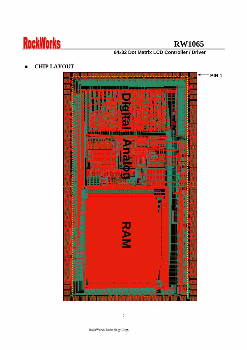
RW1065 64x32 Dot Matrix LCD Controller Driver
RockWorks Technology Corp
5
CHIP LAYOUT
PIN 1
RA
MA
nalog D
igital
RW1065 64x32 Dot Matrix LCD Controller Driver
RockWorks Technology Corp
6
PAD CENTER COORDINATES DUTY=164 duty SHL=0
Pad Pin Name Pin Name Master Slave X Y
Pad No Pin Name X Y Pad
No Master Slave X Y
1 COM13 COM45 -240475 90725 45 SEG38 11025 -90725 89 D2 205225 907252 COM14 COM46 -240475 77975 46 SEG37 20275 -90725 90 D3 19165 907253 COM15 COM47 -240475 66225 47 SEG36 29525 -90725 91 D4 18215 907254 COM16 COM48 -240475 55475 48 SEG35 38775 -90725 92 D5 17265 907255 COM17 COM49 -240475 46275 49 SEG34 48025 -90725 93 D6 16315 907256 COM18 COM50 -240475 37025 50 SEG33 57275 -90725 94 D7 15365 907257 COM19 COM51 -240475 27775 51 SEG32 66525 -90725 95 CS1BP 14415 907258 COM20 COM52 -240475 18525 52 SEG31 75775 -90725 96 CS2P 13465 907259 COM21 COM53 -240475 9275 53 SEG30 85025 -90725 97 EP 12515 9072510 COM22 COM54 -240475 025 54 SEG29 94275 -90725 98 RSP 11565 9072511 COM23 COM55 -240475 -9225 55 SEG28 103525 -90725 99 RWP 10615 9072512 COM24 COM56 -240475 -18475 56 SEG27 112775 -90725 100 VDD 9665 9072513 COM25 COM57 -240475 -27725 57 SEG26 122025 -90725 101 RSTP 8715 9072514 COM26 COM58 -240475 -36975 58 SEG25 131275 -90725 102 CLSP 7765 9072515 COM27 COM59 -240475 -46225 59 SEG24 140525 -90725 103 FRR 6815 9072516 COM28 COM60 -240475 -55475 60 SEG23 149775 -90725 104 MSP 5865 9072517 COM29 COM61 -240475 -66225 61 SEG22 159025 -90725 105 BS1P 4915 9072518 COM30 COM62 -240475 -77975 62 SEG21 168275 -90725 106 BS0P 3965 9072519 COM31 COM63 -240475 -90725 63 SEG20 177525 -90725 107 SHLP 3015 9072520 SEG63 -227725 -90725 64 SEG19 186775 -90725 108 VDD2 2065 9072521 SEG62 -214975 -90725 65 SEG18 196025 -90725 109 CAP2N 1115 9072522 SEG61 -203225 -90725 66 SEG17 205225 -90725 110 CAP2P 165 9072523 SEG60 -192475 -90725 67 SEG16 215975 -90725 111 CAP1P -785 9072524 SEG59 -183225 -90725 68 SEG15 227725 -90725 112 CAP1N -1735 9072525 SEG58 -173975 -90725 69 SEG14 240475 -90725 113 CAP3P -2685 9072526 SEG57 -164725 -90725 70 SEG13 240475 -77975 114 VOUT -3635 9072527 SEG56 -155475 -90725 71 SEG12 240475 -65225 115 V0 -4585 9072528 SEG55 -146225 -90725 72 SEG11 240475 -53475 116 VRAB -5535 9072529 SEG54 -136975 -90725 73 SEG10 240475 -42725 117 V3 -6485 9072530 SEG53 -127725 -90725 74 SEG9 240475 -33475 118 V2 -7435 9072531 SEG52 -118475 -90725 75 SEG8 240475 -24225 119 V4 -8385 9072532 SEG51 -109225 -90725 76 SEG7 240475 -14975 120 V1 -9335 9072533 SEG50 -99975 -90725 77 SEG6 240475 -5725 121 COM0 COM32 -10285 9072534 SEG49 -90725 -90725 78 SEG5 240475 3525 122 COM1 COM33 -11235 9072535 SEG48 -81475 -90725 79 SEG4 240475 12775 123 COM2 COM34 -12185 9072536 SEG47 -72225 -90725 80 SEG3 240475 22025 124 COM3 COM35 -13135 9072537 SEG46 -62975 -90725 81 SEG2 240475 31275 125 COM4 COM36 -14085 9072538 SEG45 -53725 -90725 82 SEG1 240475 40525 126 COM5 COM37 -15035 9072539 SEG44 -44475 -90725 83 SEG0 240475 51275 127 COM6 COM38 -15985 9072540 SEG43 -35225 -90725 84 ADCP 240475 63025 128 COM7 COM39 -16935 9072541 SEG42 -25975 -90725 85 CLL 240475 75775 129 COM8 COM40 -17885 9072542 SEG41 -16725 -90725 86 VSS 240475 90725 130 COM9 COM41 -192475 9072543 SEG40 -7475 -90725 87 D0 227725 90725 131 COM10 COM42 -203225 9072544 SEG39 1775 -90725 88 D1 215975 90725 132 COM11 COM43 -214975 90725 133 COM12 COM44 -227725 90725
RW1065 64x32 Dot Matrix LCD Controller Driver
RockWorks Technology Corp
7
PAD CENTER COORDINATES DUTY=164 duty SHL=1
Pad Pin Name Pin Name Master Slave X Y
Pad No Pin Name X Y Pad
No Master Slave X Y
1 COM50 COM18 -240475 90725 45 SEG38 11025 -90725 89 D2 205225 907252 COM49 COM17 -240475 77975 46 SEG37 20275 -90725 90 D3 19165 907253 COM48 COM16 -240475 66225 47 SEG36 29525 -90725 91 D4 18215 907254 COM47 COM15 -240475 55475 48 SEG35 38775 -90725 92 D5 17265 907255 COM46 COM14 -240475 46275 49 SEG34 48025 -90725 93 D6 16315 907256 COM45 COM13 -240475 37025 50 SEG33 57275 -90725 94 D7 15365 907257 COM44 COM12 -240475 27775 51 SEG32 66525 -90725 95 CS1BP 14415 907258 COM43 COM11 -240475 18525 52 SEG31 75775 -90725 96 CS2P 13465 907259 COM42 COM10 -240475 9275 53 SEG30 85025 -90725 97 EP 12515 9072510 COM41 COM9 -240475 025 54 SEG29 94275 -90725 98 RSP 11565 9072511 COM40 COM8 -240475 -9225 55 SEG28 103525 -90725 99 RWP 10615 9072512 COM39 COM7 -240475 -18475 56 SEG27 112775 -90725 100 VDD 9665 9072513 COM38 COM6 -240475 -27725 57 SEG26 122025 -90725 101 RSTP 8715 9072514 COM37 COM5 -240475 -36975 58 SEG25 131275 -90725 102 CLSP 7765 9072515 COM36 COM4 -240475 -46225 59 SEG24 140525 -90725 103 FRR 6815 9072516 COM35 COM3 -240475 -55475 60 SEG23 149775 -90725 104 MSP 5865 9072517 COM34 COM2 -240475 -66225 61 SEG22 159025 -90725 105 BS1P 4915 9072518 COM33 COM1 -240475 -77975 62 SEG21 168275 -90725 106 BS0P 3965 9072519 COM32 COM0 -240475 -90725 63 SEG20 177525 -90725 107 SHLP 3015 9072520 SEG63 -227725 -90725 64 SEG19 186775 -90725 108 VDD2 2065 9072521 SEG62 -214975 -90725 65 SEG18 196025 -90725 109 CAP2N 1115 9072522 SEG61 -203225 -90725 66 SEG17 205225 -90725 110 CAP2P 165 9072523 SEG60 -192475 -90725 67 SEG16 215975 -90725 111 CAP1P -785 9072524 SEG59 -183225 -90725 68 SEG15 227725 -90725 112 CAP1N -1735 9072525 SEG58 -173975 -90725 69 SEG14 240475 -90725 113 CAP3P -2685 9072526 SEG57 -164725 -90725 70 SEG13 240475 -77975 114 VOUT -3635 9072527 SEG56 -155475 -90725 71 SEG12 240475 -65225 115 V0 -4585 9072528 SEG55 -146225 -90725 72 SEG11 240475 -53475 116 VRAB -5535 9072529 SEG54 -136975 -90725 73 SEG10 240475 -42725 117 V3 -6485 9072530 SEG53 -127725 -90725 74 SEG9 240475 -33475 118 V2 -7435 9072531 SEG52 -118475 -90725 75 SEG8 240475 -24225 119 V4 -8385 9072532 SEG51 -109225 -90725 76 SEG7 240475 -14975 120 V1 -9335 9072533 SEG50 -99975 -90725 77 SEG6 240475 -5725 121 COM63 COM31 -10285 9072534 SEG49 -90725 -90725 78 SEG5 240475 3525 122 COM62 COM30 -11235 9072535 SEG48 -81475 -90725 79 SEG4 240475 12775 123 COM61 COM29 -12185 9072536 SEG47 -72225 -90725 80 SEG3 240475 22025 124 COM60 COM28 -13135 9072537 SEG46 -62975 -90725 81 SEG2 240475 31275 125 COM59 COM27 -14085 9072538 SEG45 -53725 -90725 82 SEG1 240475 40525 126 COM58 COM26 -15035 9072539 SEG44 -44475 -90725 83 SEG0 240475 51275 127 COM57 COM25 -15985 9072540 SEG43 -35225 -90725 84 ADCP 240475 63025 128 COM56 COM24 -16935 9072541 SEG42 -25975 -90725 85 CLL 240475 75775 129 COM55 COM23 -17885 9072542 SEG41 -16725 -90725 86 VSS 240475 90725 130 COM54 COM22 -192475 9072543 SEG40 -7475 -90725 87 D0 227725 90725 131 COM53 COM21 -203225 9072544 SEG39 1775 -90725 88 D1 215975 90725 132 COM52 COM20 -214975 90725 133 COM51 COM19 -227725 90725
RW1065 64x32 Dot Matrix LCD Controller Driver
RockWorks Technology Corp
8
PAD CENTER COORDINATES DUTY=132 duty SHL=0
Pad Pin Name Pin Name Master Slave X Y
Pad No Pin Name X Y Pad
No Master Slave X Y
1 COM13 COM29 -240475 90725 45 SEG38 11025 -90725 89 D2 205225 907252 COM14 COM30 -240475 77975 46 SEG37 20275 -90725 90 D3 19165 907253 COM15 COM31 -240475 66225 47 SEG36 29525 -90725 91 D4 18215 907254 NC NC -240475 55475 48 SEG35 38775 -90725 92 D5 17265 907255 NC NC -240475 46275 49 SEG34 48025 -90725 93 D6 16315 907256 NC NC -240475 37025 50 SEG33 57275 -90725 94 D7 15365 907257 NC NC -240475 27775 51 SEG32 66525 -90725 95 CS1BP 14415 907258 NC NC -240475 18525 52 SEG31 75775 -90725 96 CS2P 13465 907259 NC NC -240475 9275 53 SEG30 85025 -90725 97 EP 12515 9072510 NC NC -240475 025 54 SEG29 94275 -90725 98 RSP 11565 9072511 NC NC -240475 -9225 55 SEG28 103525 -90725 99 RWP 10615 9072512 NC NC -240475 -18475 56 SEG27 112775 -90725 100 VDD 9665 9072513 NC NC -240475 -27725 57 SEG26 122025 -90725 101 RSTP 8715 9072514 NC NC -240475 -36975 58 SEG25 131275 -90725 102 CLSP 7765 9072515 NC NC -240475 -46225 59 SEG24 140525 -90725 103 FRR 6815 9072516 NC NC -240475 -55475 60 SEG23 149775 -90725 104 MSP 5865 9072517 NC NC -240475 -66225 61 SEG22 159025 -90725 105 BS1P 4915 9072518 NC NC -240475 -77975 62 SEG21 168275 -90725 106 BS0P 3965 9072519 NC NC -240475 -90725 63 SEG20 177525 -90725 107 SHLP 3015 9072520 SEG63 -227725 -90725 64 SEG19 186775 -90725 108 VDD2 2065 9072521 SEG62 -214975 -90725 65 SEG18 196025 -90725 109 CAP2N 1115 9072522 SEG61 -203225 -90725 66 SEG17 205225 -90725 110 CAP2P 165 9072523 SEG60 -192475 -90725 67 SEG16 215975 -90725 111 CAP1P -785 9072524 SEG59 -183225 -90725 68 SEG15 227725 -90725 112 CAP1N -1735 9072525 SEG58 -173975 -90725 69 SEG14 240475 -90725 113 CAP3P -2685 9072526 SEG57 -164725 -90725 70 SEG13 240475 -77975 114 VOUT -3635 9072527 SEG56 -155475 -90725 71 SEG12 240475 -65225 115 V0 -4585 9072528 SEG55 -146225 -90725 72 SEG11 240475 -53475 116 VRAB -5535 9072529 SEG54 -136975 -90725 73 SEG10 240475 -42725 117 V3 -6485 9072530 SEG53 -127725 -90725 74 SEG9 240475 -33475 118 V2 -7435 9072531 SEG52 -118475 -90725 75 SEG8 240475 -24225 119 V4 -8385 9072532 SEG51 -109225 -90725 76 SEG7 240475 -14975 120 V1 -9335 9072533 SEG50 -99975 -90725 77 SEG6 240475 -5725 121 COM0 COM16 -10285 9072534 SEG49 -90725 -90725 78 SEG5 240475 3525 122 COM1 COM17 -11235 9072535 SEG48 -81475 -90725 79 SEG4 240475 12775 123 COM2 COM18 -12185 9072536 SEG47 -72225 -90725 80 SEG3 240475 22025 124 COM3 COM19 -13135 9072537 SEG46 -62975 -90725 81 SEG2 240475 31275 125 COM4 COM20 -14085 9072538 SEG45 -53725 -90725 82 SEG1 240475 40525 126 COM5 COM21 -15035 9072539 SEG44 -44475 -90725 83 SEG0 240475 51275 127 COM6 COM22 -15985 9072540 SEG43 -35225 -90725 84 ADCP 240475 63025 128 COM7 COM23 -16935 9072541 SEG42 -25975 -90725 85 CLL 240475 75775 129 COM8 COM24 -17885 9072542 SEG41 -16725 -90725 86 VSS 240475 90725 130 COM9 COM25 -192475 9072543 SEG40 -7475 -90725 87 D0 227725 90725 131 COM10 COM26 -203225 9072544 SEG39 1775 -90725 88 D1 215975 90725 132 COM11 COM27 -214975 90725 133 COM12 COM28 -227725 90725
RW1065 64x32 Dot Matrix LCD Controller Driver
RockWorks Technology Corp
9
PAD CENTER COORDINATES DUTY=132 duty SHL=1
Pad Pin Name Pin Name Master Slave X Y
Pad No Pin Name X Y Pad
No Master Slave X Y
1 COM18 COM2 -240475 90725 45 SEG38 11025 -90725 89 D2 205225 907252 COM17 COM1 -240475 77975 46 SEG37 20275 -90725 90 D3 19165 907253 COM16 COM0 -240475 66225 47 SEG36 29525 -90725 91 D4 18215 907254 NC NC -240475 55475 48 SEG35 38775 -90725 92 D5 17265 907255 NC NC -240475 46275 49 SEG34 48025 -90725 93 D6 16315 907256 NC NC -240475 37025 50 SEG33 57275 -90725 94 D7 15365 907257 NC NC -240475 27775 51 SEG32 66525 -90725 95 CS1BP 14415 907258 NC NC -240475 18525 52 SEG31 75775 -90725 96 CS2P 13465 907259 NC NC -240475 9275 53 SEG30 85025 -90725 97 EP 12515 9072510 NC NC -240475 025 54 SEG29 94275 -90725 98 RSP 11565 9072511 NC NC -240475 -9225 55 SEG28 103525 -90725 99 RWP 10615 9072512 NC NC -240475 -18475 56 SEG27 112775 -90725 100 VDD 9665 9072513 NC NC -240475 -27725 57 SEG26 122025 -90725 101 RSTP 8715 9072514 NC NC -240475 -36975 58 SEG25 131275 -90725 102 CLSP 7765 9072515 NC NC -240475 -46225 59 SEG24 140525 -90725 103 FRR 6815 9072516 NC NC -240475 -55475 60 SEG23 149775 -90725 104 MSP 5865 9072517 NC NC -240475 -66225 61 SEG22 159025 -90725 105 BS1P 4915 9072518 NC NC -240475 -77975 62 SEG21 168275 -90725 106 BS0P 3965 9072519 NC NC -240475 -90725 63 SEG20 177525 -90725 107 SHLP 3015 9072520 SEG63 -227725 -90725 64 SEG19 186775 -90725 108 VDD2 2065 9072521 SEG62 -214975 -90725 65 SEG18 196025 -90725 109 CAP2N 1115 9072522 SEG61 -203225 -90725 66 SEG17 205225 -90725 110 CAP2P 165 9072523 SEG60 -192475 -90725 67 SEG16 215975 -90725 111 CAP1P -785 9072524 SEG59 -183225 -90725 68 SEG15 227725 -90725 112 CAP1N -1735 9072525 SEG58 -173975 -90725 69 SEG14 240475 -90725 113 CAP3P -2685 9072526 SEG57 -164725 -90725 70 SEG13 240475 -77975 114 VOUT -3635 9072527 SEG56 -155475 -90725 71 SEG12 240475 -65225 115 V0 -4585 9072528 SEG55 -146225 -90725 72 SEG11 240475 -53475 116 VRAB -5535 9072529 SEG54 -136975 -90725 73 SEG10 240475 -42725 117 V3 -6485 9072530 SEG53 -127725 -90725 74 SEG9 240475 -33475 118 V2 -7435 9072531 SEG52 -118475 -90725 75 SEG8 240475 -24225 119 V4 -8385 9072532 SEG51 -109225 -90725 76 SEG7 240475 -14975 120 V1 -9335 9072533 SEG50 -99975 -90725 77 SEG6 240475 -5725 121 COM31 COM15 -10285 9072534 SEG49 -90725 -90725 78 SEG5 240475 3525 122 COM30 COM14 -11235 9072535 SEG48 -81475 -90725 79 SEG4 240475 12775 123 COM29 COM13 -12185 9072536 SEG47 -72225 -90725 80 SEG3 240475 22025 124 COM28 COM12 -13135 9072537 SEG46 -62975 -90725 81 SEG2 240475 31275 125 COM27 COM11 -14085 9072538 SEG45 -53725 -90725 82 SEG1 240475 40525 126 COM26 COM10 -15035 9072539 SEG44 -44475 -90725 83 SEG0 240475 51275 127 COM25 COM9 -15985 9072540 SEG43 -35225 -90725 84 ADCP 240475 63025 128 COM24 COM8 -16935 9072541 SEG42 -25975 -90725 85 CLL 240475 75775 129 COM23 COM7 -17885 9072542 SEG41 -16725 -90725 86 VSS 240475 90725 130 COM22 COM6 -192475 9072543 SEG40 -7475 -90725 87 D0 227725 90725 131 COM21 COM5 -203225 9072544 SEG39 1775 -90725 88 D1 215975 90725 132 COM20 COM4 -214975 90725 133 COM19 COM3 -227725 90725
RW1065 64x32 Dot Matrix LCD Controller Driver
RockWorks Technology Corp
10
Pin Description
(1)Power Pins
Name IO Description
VDD - Connected to the +5V 0r +3V dc power Common to the Vcc MPU power pin
VDD2 This is the retevence power supply for the Step-up voltage circuit
VSS - 0V dc pin connected to the system ground
CAP1P~3P CAP1N~2N - Capacitor connector pin for voltage booster
V0~V4 - Multi-level power supplies for LCD driving The voltage determined for each liquid crystal cell is divided by resistance or it is converted in impedance by the op amp and supplied These voltages must satisfy the following V0 ≧ V1 ≧ V2 ≧ V3 ≧V4 ≧ VSS
(2)System Bus Connection Pins Name IO Description
D7 to D0 IO The 8-bit bidirectional data buses to be connected to the 8- or 16- bit standard MCU Data busses
RS I Usually connected to the low-order bit of the MPU address bus and used to identify the data or a command RS=0 D0 to D7 are display control data RS=1 D0 to D7 are display data
CLS I CLS=1 internal oscillator enable CLS=0 external clock operation mode
ADCP I
The pin selects the relationship between display data RAM column addresses and segment drivers ADCP=1 SEG0larrcolumn address 3FHhellipinverted ADCP=0 SEG0larrcolumn address 00Hhellipnormal
SHLP I
The pin selects the com output scan direction SHL=1 Reverse directioncom63rarrcom0 SHL=0 Normal com0rarrcom63 Both master and slave should set identical SHL value
BS1PBS0P I
Select LCD Bias 15 16 18 19 bias BS1P=0 BS0P=0 15 bias BS1P=0 BS0P=1 16 bias BS1P=1 BS0P=0 18 bias BS1P=1 BS0P=1 19 bias
RST ―
I Input low active System reset
CS1BP CS2P I Input When CS1BP = 0 and CS2P = 1 the chip select become active
E I For 68-series MPU Input Active high
Used as an enable clock input of the 68-series MPU
RW I For 68-series MPU Input
Used as an input pin of read control signals (if RW is high) or write control signals signals (if low)
RW1065 64x32 Dot Matrix LCD Controller Driver
RockWorks Technology Corp
11
(3)LCD Driver Circuit Signals
Name IO Description
CLL IO
Inputoutput IO selection
MS = ldquoHrdquo amp CLS = ldquoHrdquo Output MS = ldquoLrdquo amp CLS = ldquoHrdquo Input MS = ldquoXrdquo amp CLS = ldquoLrdquo Input
This is a display data latch signal to count up the line counter and common counterat each signal falling and rising edges
SEGn O Output A single level of V0 V2 V3 and VSS is selected by the combination of display RAM contents and FR signal
COMn O Output The output pin for LCD common (row) driving A single level of V0 V1 V4 and VSS is selected by the combination of common counter output and FR signal The slave LSI has the reverse common output scan sequence than the master LSI
FRR IO
Inputoutput This is the liquid crystal alternating current signal IO terminal lO selection
MS = ldquoHrdquoOutput MS = ldquoLrdquoInput
VRAB I Provides the voltage between V0 and VSS through a resistive voltage divider
MS I
Input The master or slave LSI operation select pin for the RW1065
MS OperatingMode FR CL V0~V4 Power
SupplyInternal
OSC COMMON
Output SEG
output
High Master Output See CLS On On See
CLS COM0-31 SEG0-63
Low Slave Input Input Off Off Off COM32-63
SEG64-127
RW1065 64x32 Dot Matrix LCD Controller Driver
RockWorks Technology Corp
12
DESCRIPTION OF FUNCTIONS
The Parallel Interface (6800 series MPU)
Shared 6800 Series
RS RW Function
1 1 Reads the display data
1 0 Writes the display data
0 1 Status read
0 0 Write control data (command)
The Chip Select The RW1065 Series chips have two chip select terminals CS1
―BP and CS2P
When the chip select is inactive D0 to D7 enter a high impedance state and the RS E and RW inputs are inactive
The Accessing the Display Data RAM and the Internal Registers Data transfer at a higher speed is ensured since the MPU is required to satisfy the cycle time (tCYC) requirement alone in accessing the RW1065 Series Wait time may not be considered And in the RW1065 Series chips each time data is sent from the MPU a type of pipeline process between LSIs is performed through the bus holder attached to the internal data bus Internal data bus For example when the MPU writes data to the display data RAM once the data is stored in the bus holder then it is written to the display data RAM before the next data write cycle Moreover when the MPU reads the display data RAM
the first data read cycle (dummy) stores the read data in the bus holder and then the data is read from the bus holder to the system bus at the next data read cycle There is a certain restriction in the read sequence of the display data RAM Please be advised that data of the specified address is not generated by the read instruction issued immediately after the address setup This data is generated in data read of the second time Thus a dummy read is required whenever the address setup or write cycle operation is conducted This relationship is shown in Figure 2
RW1065 64x32 Dot Matrix LCD Controller Driver
RockWorks Technology Corp
13
E
Fig 2b read timing
E
RW
Fig 2a write timing (RW=rdquoLrdquo)
RS
RS
RW1065 64x32 Dot Matrix LCD Controller Driver
RockWorks Technology Corp
14
Display Data RAM The display data RAM is a RAM that stores the dot data for the display It has a 64 (8 page x 8 bit) x 64 bit structure It is possible to access the desired bit by specifying the page address and the column addressBecause as is shown in Figure 3 the D7 to D0 display data from the MPU corresponds to the liquid crystal display common direction there are few constraints at the time of display data transfer when multiple RW1065 series chips are used
thus and display structures can be created easily and with a high degree of freedom Moreover reading from and writing to the display RAM from the MPU side is performed through the IO buffer which is an independent operation from signal reading for the liquid crystal driver Consequently even if the display data RAM is accessed asynchronously during liquid crystal display it will not cause adverse effects on the display (such as flickering)
0
1
0
0
1
1
0
0
1
0
1
0
0
1
0
1
0
0
1
0
0
0
0
0
0
D0
D1
D2
D3
D4
-
Display data RAM Liquid crystal display
COM0
COM1
COM2
COM3
COM4
-
Figure3
The Page Address Circuit As shown in Figure 4 page address of the display data RAM is specified through the Page Address Set Command The page address must be specified again when changing pages to perform access
The Column Address As is shown in Table 4 the display data RAM column address is specified by the Column Address Set command The specified column address is incremented (+1) with each display data readwrite command This allows the MPU display data to be accessed continuously Moreover the increment of column addresses stops with 3FH Because the column address is independent of the page address when moving for example from page 0 column 3FH to page 1
column 00H it is necessary to respecify both the page address and the column address Furthermore as is shown in Table 4 the ADC command (segment driver direction select command) can be used to reverse the relationship between the display data RAM column address and the segment output Because of this the constraints on the IC layout when the LCD module is assembled can be minimized
Table 4 SEG Output
ADC set SEG0 SEG 63
ADC(D0)=0 0 rarr Column Address rarr 63 ADC(D0)=1 63 larr Column Address larr 0
RW1065 64x32 Dot Matrix LCD Controller Driver
RockWorks Technology Corp
15
Figure 4
Page Address D3 D2 D1 D0
DataSE
G0
SEG
1
SEG
2
SEG
3
SEG
4
SEG
5
SEG
6
SEG
7
SEG
8
helliphelliphelliphellip
SEG
55
SEG
56
SEG
57
SEG
58
SEG
59
SEG
60
SEG
61
SEG
62
SEG
63 SEG
COM
D0 COM0
D1 COM1
D2 COM2
D3 COM3
D4 COM4
D5 COM5
D6 COM6
0 0 0 0
D7
Page 0
COM7
D0 COM8
D1 COM9
D2 COM10
D3 COM11
D4 COM12
D5 COM13
D6 COM14
0 0 0 1
D7
Page 1
COM15
D0 COM16
D1 COM17
D2 COM18
D3 COM19
D4 COM20
D5 COM21
D6 COM22
0 0 1 0
D7
Page 2
COM23
D0 COM24
D1 COM25
D2 COM26
D3 COM27
D4 COM28
D5 COM29
D6 COM30
0 0 1 1
D7
Page 3
COM31
ADC=0 00
01
02
03
04
05
06
07
08
helliphelliphelliphellip 55
56
57
58
59
60
61
62
63
COLUMN ADC=1 63
62
61
60
59
58
57
56
55
helliphelliphelliphellip 08
07
06
05
04
03
02
01
00
RW1065 64x32 Dot Matrix LCD Controller Driver
RockWorks Technology Corp
16
Common Timing Generator Circuit Display Data Latch Circuit Generates common timing signals and FR frame signals from the CL basic clock The 132 or 164 duty (for RW1065) can be selected by the Duty Select command The 132 and 164 duties are provided by two chips consisting of the master and slave chips in the common multi-chip mode
This latch stores one line of display data for use by the LCD driver interface circuitry The output of this latch is controlled by the Display ONOFF
132 duty
164 duty
SHL=0
SHL=1
SHL=0
SHL=1
RW1065 64x32 Dot Matrix LCD Controller Driver
RockWorks Technology Corp
17
Display Timing Generator Circuit
The display timing generator circuit generates the timing signal to the line address circuit and the display data latch circuit using the display clock The display data is latched into the display data latch circuit synchronized with the display clock and is output to the data driver output terminal Reading to the display data liquid crystal driver circuits is completely independent of accesses to the display data RAM by the MPU Consequently even if the display data
RAM is accessed asynchronously during liquid crystal display there is absolutely no adverse effect (such asflickering) on the display Moreover the display timing generator circuit generates the common timing and the liquid crystal alternating current signal (FR) from the display clock It generates a drive wave form using a 2 frame alternating current drive method as is shown in Figure 5 for the liquid crystal drive circuit
Two-frame alternating current drive waveform
Figure 5
When multiple RW1065 Series chips are used the slave chip must be supplied the display timing signals(FR CL) from the master chip
Table 5 shows the status of the FR and CL signals
Table 5 Operating Mode FR CL
Master (MS = ldquoHrdquo) The internal oscillator circuit is enabled (CLS = ldquoHrdquo) The internal oscillator circuit is disabled (CLS = ldquoLrdquo)
Output Output
Output Input
Slave (MS = ldquoLrdquo) The internal oscillator circuit is enabled (CLS = ldquoHrdquo) The internal oscillator circuit is disabled (CLS = ldquoLrdquo)
Input Input
Input Input
RW1065 64x32 Dot Matrix LCD Controller Driver
RockWorks Technology Corp
18
The Liquid Crystal Driver Circuits
These are a 64-channel (RW1065) that generate four voltage levels for driving the liquid crystal The combination of the display data the COM scan signal and the FR signal
produces the liquid crystal drive voltage output Figure 6 shows examples of the SEG and COM output waveform
Figure 6
RW1065 64x32 Dot Matrix LCD Controller Driver
RockWorks Technology Corp
19
The Power Supply Circuit
The power supply circuits are low-power consumption power supply circuits that generate the voltage levels required for the liquid crystal drivers They comprise Booster circuits and voltage follower circuits They are only enabled in master operation The power supply circuits can turn on automatically after power on
Consequently it is possible to make an external power supply and the internal power supply function somewhat in parallel
The Liquid Crystal Voltage Generator Circuit The V0 voltage is produced by a resistive voltage divider outside the IC through VRAB pin and can be produced at the V1 V2 V3 and V4 voltage levels required for liquid crystal driving Moreover when the voltage follower changes the impedance it provides V1 V2 V3 and V4 to the liquid crystal drive circuit 15 bias or 16 bias or 18 bias or 19 bias for RW1065 can be selected by BS0 and BS1 pins V0-Vss maximum voltage is 15V Vout-Vss maximum voltage is 17V If VDD lt 35V it can use the Booster circuit 2x3x4xThe booster voltage can follow the spec condition (Vout-Vss ≦ 17V max voltage) if VDD gt35V only use the 2X3X booster circuit that can ensure the V0-Vss voltage ≦ 15V If use the VDD voltage 5V and 4X booster itrsquos over the spec operation condition To turn on built-in power (boosterfollower) must waiting 200mS to display on for boosterfollower stable Therefore power off must follower ldquopower off sequencerdquo too
Power on Display off
Power off
Power off sequence
Wait time gt200mS
Display on
Power on sequence
RW1065 64x32 Dot Matrix LCD Controller Driver
RockWorks Technology Corp
20
The Reset Circuit
When the RTP input comes to the ldquoLrdquo level these LSIs return to the default state Their default states are as follows 1 Display OFF 2 Display all point on is select to normal 3 Display normalreverse is select to normal 4 164 duty is selected 5 Read modify write OFF 6 Column address set to Address 0 7 Page address set to Page 0 8 Start line set to first line 9 Frame frequency set to default 10 Power save mode released 11 Ext set to ldquo0rdquo When the power is turned on the IC internal state becomes unstable and it is necessary to initialize it using the RSTP terminal After the initialization each input terminal should be controlled normally While RSTP is ldquoLrdquo the oscillator works but the display timing generator stops and the CL FR terminals are fixed to ldquoHrdquo The terminals D0 to D7 are not affected
RW1065 64x32 Dot Matrix LCD Controller Driver
RockWorks Technology Corp
21
TABLE OF RW1065 INSTRUCTIONS
Instruction code Instruction RS RW DB7 DB6 DB5 DB4 DB3 DB2 DB1 DB0 Description
EXT=0 or 1
MODE SET 0 0 0 0 0 0 1 1 0 EXT Set EXT mode
Instruction code Instruction RS RW DB7 DB6 DB5 DB4 DB3 DB2 DB1 DB0 Description
EXT=0 Display ONOFF 0 0 0 0 1 1 1 1 1 D D=0Display OFF
D=1Display ONSet page address 0 0 1 0 1 1 1 P2 P1 P0 Set page address
Set column address 0 0 0 1 Y5 Y4 Y3 Y2 Y1 Y0 Set column
address MSB
Read Status 0 1 BUSY 0 ON OFF RESET 0 0 0 0 Read register
status Write display
data 1 0 Write data Write data into DDRAM
Read display data 1 1 Read data Read data from
DDRAM Set initial
display line register
0 0 1 1 S5 S4 S3 S2 S1 S0 Specify the initial
display line to realize vertical scrolling
Instruction code Instruction RS RW DB7 DB6 DB5 DB4 DB3 DB2 DB1 DB0 Description
EXT=1
NOP 0 0 0 0 0 0 0 0 0 0 no operation
Set modiy-read 0 0 0 0 0 0 1 0 0 0 Set modiy-read
mode
END 0 0 0 0 0 0 1 1 1 0 release modiy-read mode
Set power save mode 0 0 0 0 0 0 0 0 1 PSAVE P=0 normal mode
P=1 sleep mode
0 0 0 0 0 1 0 1 Display
COMMAND (double
command)
0 0 FRSEL
0 0 0 0 REV ALLON DUTY
DUTY=1 64 duty DUTY=0 32 duty ALLON=1display all on ALLON=0display
normal REV=1display reverse REV=0display normal FRSEL=1FR frequency double default FRSEL=0FR frequency default
RW1065 64x32 Dot Matrix LCD Controller Driver
RockWorks Technology Corp
22
Command Description
See the Table of RW1065 instructions The RW1065 series identifies a data bus using a combination of RS E and RW signals As the MPU translates a command in the internal timing only (independent from the external clock) its speed is very high The busy check is usually not required
Display ONOFF
EXT RS RW D7 D6 D5 D4 D3 D2 D1 D0
0 0 0 0 0 1 1 1 1 1 D
This command turns the display on and off D=1 Display ON D=0 Display OFF(default)
Set page Address This command specifies the page address that corresponds to the low address of the display data RAM when it is accessed by the MPU Any bit of the display data RAM can be accessed when its page address and column address are specified The display status is not changed even when the page address is changed
EXT RS RW D7 D6 D5 D4 D3 D2 D1 D0
0 0 0 1 0 1 1 1 A2 A1 A0
This command loads the page address register
A2 A1 A0 Page
0 0 0 0 (default)
0 0 1 1 0 1 0 2 0 1 1 3 1 0 0 4 1 0 1 5 1 1 0 6 1 1 1 7
Page mapping see Figure 4
RW1065 64x32 Dot Matrix LCD Controller Driver
RockWorks Technology Corp
23
Set Column Address This command specifies a column address of the display data RAM When the display data RAM is accessed by the MPU continuously the column address is incremented by I each time it is accessed from the set address Therefore the MPU can access to data continuously The column address stops to be incremented at address 63 and the page address is not changed continuously
EXT RS RW D7 D6 D5 D4 D3 D2 D1 D0
0 0 0 0 1 A5 A4 A3 A2 A1 A0
A5 A4 A3 A2 A1 A0 Column Address0 0 0 0 0 0 0(default) 0 0 0 0 0 1 1
1 1 1 1 1 1 63
Read Status
EXT RS RW D7 D6 D5 D4 D3 D2 D1 D0
0 0 1 BUSY 0 ON OFF RESET 0 0 0 0
The BUSY Flag bit indicates that RW 1065 is operating or no operating
BUSY=1 Operation BUSY=0 Ready
The ONOFF bit indicates the current status of the display It is the inverse of the polarity of the display ONOFF command ONOFF=1 Display OFF ONOFF=0 Display ON The RESET bit indicates whether the driver is executing a hardware or software reset or if it is in normal operating mode RESET=1 Currently executing reset command RESET=0 Normal operation
RW1065 64x32 Dot Matrix LCD Controller Driver
RockWorks Technology Corp
24
Write Display Data
EXT RS RW D7 D6 D5 D4 D3 D2 D1 D0
0 1 0 Write data
Writes 8-bits of data into the display data RAM at a location specified by the contents of the column address and page address registers and then increments the column address register by one
Read Display Data
EXT RS RW D7 D6 D5 D4 D3 D2 D1 D0
0 1 1 Read data
Reads 8-bits of data from the data IO latch updates the contents of the IO latch with display data from the display data RAM location specified by the contents of the column address and page address registers and then increments the column address register After loading a new address into the column address register one dummy read is required before valid data is obtained
Set initial display line register
EXT RS RW D7 D6 D5 D4 D3 D2 D1 D0
0 0 0 1 1 S5 S4 S3 S2 S1 S0
Loads the RAM line address of the initial display line COM 0 into the initial display line register The RAM display data becomes the top line of the LCD screen It is followed by the higher number lines in ascending order corresponding to the duty cycle The screen can be scrolled using this command by incrementing the line address(default value=rdquo00Hrdquo)
RW1065 64x32 Dot Matrix LCD Controller Driver
RockWorks Technology Corp
25
Read-Modify-Write
EXT RS RW D7 D6 D5 D4 D3 D2 D1 D0
1 0 0 0 0 0 0 1 0 0 0
This command defeats column address register auto-increment after data reads The current contents of the column Address register are saved The mode remains active until an End command is received When the End command is entered the column address is returned to the one used during input of Read-Modify-Write Command This function can reduce the load of MPU when data change is repeated as a specific display area Any command other than Data Read or Write can be used in the Read-Modify-Write mode However the Column Address Set command cannot be used
End
EXT RS RW D7 D6 D5 D4 D3 D2 D1 D0
1 0 0 0 0 0 0 1 1 1 0
This command cancels read-modify-write mode and restores the contents of the column address register to their value prior to the receipt of the Read-Modify-Write command
N N+1 N+2 N+3 N+m N
Read -modify-write mode set End
Returm
Column address
Set page address
Set column address
Read-modify-write
Dummy read
Read data
Write data
End
CompletedNo
Yes
RW1065 64x32 Dot Matrix LCD Controller Driver
RockWorks Technology Corp
26
Set power save mode
EXT RS RW D7 D6 D5 D4 D3 D2 D1 D0
1 0 0 0 0 0 0 0 0 1 PSAVE
When power save mode is entered thus greatly reducing power consumption In the power save mode the display data is saved as is the operating mode that was in effect before the power saver mode was initiated and the MPU is still able to access the display data RAM PSAVE=1 Sleep mode PSAVE=0 Normal mode Sleep mode This stops all operations in the LCD display system and as long as there are no accesses from the MPU the consumption current is reduced to a value near the static current The internal modes during sleep mode are as follows 1 The oscillator circuit and the LCD power supply circuit are halted 2 All liquid crystal drive circuits are halted and the segment and common drive outputs output a Vss level
Display command double command
EXT RS RW D7 D6 D5 D4 D3 D2 D1 D0
1 0 0 0 0 0 0 0 1 0 1
1 0 0 FRSEL 0 0 0 0 REV ALLON DUTY
Display NormalReverse set REV=1 Reverse REV=0 Normal(default) Display All Point ONOFF ALLON=1 All display points ON ALLON=0 Normal(default) Select Duty Duty=1 164 duty cycle(default) Duty=0 132 duty cycle FRAME FREQUENCY Select FRSEL=1 Double FRSEL=0 (default)
RW1065 64x32 Dot Matrix LCD Controller Driver
RockWorks Technology Corp
27
Hardware Pin Set
Select ADC by ADC Pin The pin selects the relationship between display data RAM column addresses and segment drivers ADC=1 SEG0larrcolumn address 3FHhellipinverted ADC=0 SEG0larrcolumn address 00Hhellipnormal(default) This command is provided to reduce restrictions on the placement of driver ICs and routing of traces during printed circuit Board design See Figure 4 for a table of segments and column addresses for the two values of D
Select SHL by SHL Pin The pin selects the com output scan direction SHL=1 Reverse directioncom63rarrcom0 SHL=0 Normal com0rarrcom63 Both master and slave should set identical SHL value
Select LCD Bias by BS0 BS1 Pin
BS1 BS0 Bias 0 0 15 bias 0 1 16 bias 1 0 18 bias 1 1 19 bias
RW1065 64x32 Dot Matrix LCD Controller Driver
RockWorks Technology Corp
28
When an External Resistance is Used The liquid crystal power supply voltage V0 is set by adding resistors Rarsquo and Rbrsquo between VDD and VR and between VR and V0 respectively
RW1065
RW1065 64x32 Dot Matrix LCD Controller Driver
RockWorks Technology Corp
29
The set voltage circuits
Using the step-up voltage circuits equipped within the RW1065 chips it is possible to produce a 2X 3X 4X step-up voltage levels 2X step-up
To produce voltage level in the positive direction at the Vout terminal that is 2 times the voltage difference between VSS and VDD2 Please configure set voltage circuits like this Place a 1uF~22uF capacitor between CAP1N and CAP1P Place a 1uF~22uF capacitor between VSS and VOUT Short CAP2P CAP3P and VOUT Leave CAP2N open 3X step-up
To produce voltage level in the positive direction at the Vout terminal that is 3 times the voltage difference between VSS and VDD2 Please configure set voltage circuits like this Place a 1uF~22uF capacitor between CAP1N and CAP1P Place a 1uF~22uF capacitor between VSS and VOUT Place a 1uF~22uF capacitor and 100 ohms resistor between CAP2N and CAP2P Short CAP3P and Vout 4X step-up
To produce voltage level in the positive direction at the Vout terminal that is 4 times the voltage difference between VSS and VDD2 Please configure set voltage circuits like this Place a 1uF~22uF capacitor between CAP1N and CAP1P Place a 1uF~22uF capacitor between VSS and VOUT Place a 1uF~22uF capacitor and 100 ohms resistor between CAP2N and CAP2P Place a 1uF~22uF capacitor and 100 ohms resistor between CAP1N and CAP3P
RW1065 64x32 Dot Matrix LCD Controller Driver
RockWorks Technology Corp
30
ABSOLUTE MAXIMUM RATINGS Characteristics Symbol Value Unit
Power supply voltage VDD -03 to +70 V
LCD driver voltage Vout 0 to +17 V
Input voltage VIN -03 to VDD+03 V
Operating temperature TA -40 to +85
Storage temperature TSTO -55 to +125
DC CHARACTERISTICS
Rating Item Symbol Condition Min Typ Max Unit ApplicablePin
Operating Voltage VDD - 27 30 55 V VDD1
Step up output voltage Vout (Relative to VDD) 0 - 17 V Vout
Voltage follower circuit operating Voltage V0 (Relative to VDD) 0 - 15 V V0
V0 accuracy V0 - 0 - 15 V0
High-level Input Voltage Low-level Input Voltage
VIHC VILC - 07 VDD
Vss - VDD 09 V 2
High-level Output Voltage Low-level Output Voltage
VOHC VOLC
IOH = ndash05 mA IOL = 05 mA
08VDD Vss - VDD
02 VDD V 3
Input leakage current ILI VIN = VDD or VSS -1 - 2 uA 4
Output leakage current ILO - -1 1 uA 5
Liquid Crystal Driver ON Resistance RON
Ta= 25degC(Relative To VDD)
V0 =15 V - 16 20 KΩ SEGn COMn 6
Internal Oscillator fOSC 2286 254 2794 Oscillator
Frequency External Input RECOMMAND fCL
Ta = 25degC 132Duty 2286 254 2794
kHz CL
Internal Oscillator fOSC 45 5 55 Oscillator
Frequency External Input RECOMMAND fCL
Ta = 25degC 164Duty 45 5 55
kHz CL
bullDynamic Consumption Current During Display with the Internal Power Supply OFF Current consumed by total ICs when an external power supply is used
Unless otherwise specified Vss=0V VDD=30V
RW1065 64x32 Dot Matrix LCD Controller Driver
RockWorks Technology Corp
31
Display Pattern OFF
Ta = 25degC Vout=17V Rating Item Symbol Condition Min Typ Max Unit Notes
VDD=30 V V0-Vss=8V - 10 15 RW1065 IDD VDD=50 V V0-Vss=8V - 35 45
microA 7
Display Pattern Checker
Ta = 25degC Vout=17V Rating Item Symbol Condition Min Typ Max Unit Notes
VDD=30 V V0-Vss=8V - 15 20 RW1065 IDD VDD=50 V V0-Vss=8V - 40 50
microA 7
Display Pattern OFF
Ta = 25degC Vout=17V Rating Item Symbol Condition Min Typ Max Unit Notes
VDD=30 V V0-Vss=8V - 15 20 RW1065 IDD VDD=50 V V0-Vss=8V - 40 50
microA 7
Display pattern Checker
Ta = 25degC Vout=17V Rating Item Symbol Condition Min Typ Max Unit Notes
VDD=30 V V0-Vss=8V - 65 80 RW1065 IDD VDD=50 V V0-Vss=8V - 130 150
microA 7
bull Consumption Current at Time of Power Saver Mode VSS = 0 V VDD = 30 V plusmn 10
Rating Item Symbol Condition Min Typ Max Unit Notes
Sleep mode IDD - - 5 10 microA -
References for items market with 1 While a broad range of operating voltages is guaranteed performance cannot be guaranteed if there are sudden fluctuations to the
voltage while the MPU is being accessed 2 The RS D0 to D5 D6 D7 E RW CS1BP CS2P CLS CL FR MS and RST
― terminals
3 The D0 to D7 FR and CL terminals 4 The RS E RW CS1BP CS2P CLS MS and RST
― terminals
5 Applies when the D0 to D5 D6 D7 CL and FR terminals are in a high impedance state 6 These are the resistance values for when a 01 V voltage is applied between the output terminals SEGn or COMn and
the various power supply terminals (V1 V2 V3 and V4) These are specified for the operating voltage (3) range RON = 01 V ∆I (Where ∆I is the current that flows when 01 V is applied while the power supply is ON)
7 It indicates the current consumed on ICs alone when the internal oscillator circuit and display are turned on Does not include the current due to the LCD panel capacity and wiring capacity Applicable only when there is no access from the MPU
RW1065 64x32 Dot Matrix LCD Controller Driver
RockWorks Technology Corp
32
TIMING CHARACTERISTICS
68 Interface
(Ta=-40 to 85 degC) VDD=27 to 45V
Rating VDD=45 to 55V
Rating Item Signal Symbol ConditionMin Max Min Max
Units
Address hold time RS tAH6 0 mdash 0 mdash Address setup time RS tAW6
mdash 0 mdash 0 mdash
ns
System cycle time RS tCYC6 mdash 900 mdash 800 mdash ns Data setup time D0 to D7 tDS6 100 mdash 100 mdash Data hold time D0 to D7 tDH6
mdash 0 mdash 0 mdash
ns
Access time D0 to D7 tACC6 mdash 350 mdash 250
Output disable time D0 to D7 tOH6 CL = 100 pF
mdash 300 mdash 200 ns
Read tEWHR 360 mdash 300 mdash Enable H pulse time
WriteE
tEWHW mdash
360 mdash 300 mdash ns
Read tEWLR 450 mdash 400 mdash Enable L pulse time
WriteE
tEWLW mdash
450 mdash 400 mdash ns
1 All timing is specified using 20 and 80 of VDD as the reference 2 tEWLW and tEWLR are specified as the overlap between CS1BP being ldquoLrdquo (CS2P = ldquoHrdquo) and E
RW1065 64x32 Dot Matrix LCD Controller Driver
RockWorks Technology Corp
33
Reset Timing
Rating Item Signal Symbol Condition
Min Typ Max Units
Reset time mdash tR mdash mdash - 2 micros
Reset ldquoLrdquo pulse width RST tRW mdash 2 - mdash micros
1 When double chip was be used then the duty set command must be set between the tR
RW1065 64x32 Dot Matrix LCD Controller Driver
RockWorks Technology Corp
34
IO PAD CONFIGURATION
RW1065 64x32 Dot Matrix LCD Controller Driver
RockWorks Technology Corp
35
THE MPU INTERFACE (REFERENCE EXAMPLES) The RW1065 Series can be connected to 6800 Series MPUs The display area can be enlarged by using multiple RW1065 Series chips When this is done the chip select signal can be used to select the individual ICs to access
6800 Series MPUs
RW
106
5
RW1065 64x32 Dot Matrix LCD Controller Driver
RockWorks Technology Corp
36
When using external multi-level power supply for LCD driving (REFERENCE EXAMPLE)
Using a resistor divider can provide RW1065 external multi-level power supply for LCD driving
The circuit below shows a resistor divider network which can bias V0 V1 V2 V3 and V4 externally
RW1065 64x32 Dot Matrix LCD Controller Driver
RockWorks Technology Corp
37
bullWhen V0 V1 V2 V3 and V4 are biased by external power supply analog section of RW1065 should be turn off by software during LCD initialization The example in below shows the sequence to turn off analog section when external bias is used Begin of LCD initialization 1 Reset RW1065 2 SET EXT=1 (mode instruction)
RS RW DB7 DB6 DB5 DB4 DB3 DB2 DB1 DB00 0 0 0 0 0 1 1 0 1
3 SET Display Command (double command)
RS RW DB7 DB6 DB5 DB4 DB3 DB2 DB1 DB00 0 0 0 0 0 0 1 0 1 0 0 0 0 1 1 0 0 0 1
4 SET EXT=1 (mode instruction)
RS RW DB7 DB6 DB5 DB4 DB3 DB2 DB1 DB00 0 0 0 0 0 1 1 0 0
End of LCD initialization
bullBecause pins can not set LCD bias when external power supplies are used for LCD driving the bias can be set by an appropriate configuration for a resistor voltage divider networks The example is shown below
VSS
R
R
NR
R
R
RV1
RV2
RV3
RV4
V0
Bias Network Circuit Concept 15 Bias N=1 total = 5R 16 Bias N=2 total =6R 18 Bias N=4 total =8R 19 Bias N=5 total = 9R
RW1065 64x32 Dot Matrix LCD Controller Driver
RockWorks Technology Corp
38
Single chip solution for RW1065 application (REFERENCE EXAMPLE)
For a 64x32 application the duty cycle of LCD panel is 164 and the display duty of RW1065 should be set to 164 The display duty cycle can be selected by the DUTY bit in display command The diagram for 64x32 application is shown below
64 SEGx32COM LCD Panel
164 duty cycle
RW1065 DUTY=1
COM1~33
SEG1~65
RW1065 64x32 Dot Matrix LCD Controller Driver
RockWorks Technology Corp
39
Using an adjustable resistor on the main board to adjust the contrast of liquid crystal display (REFERENCE EXAMPLE)
The schematic shows an adjustable resistor on main board that can adjust voltage level of V0
RW1065 64x32 Dot Matrix LCD Controller Driver
RockWorks Technology Corp
40
Package information (Please pay close attention to the information in this section Do not hesitate to consult with our sale representative if you have any question or concern)
In order to make better bonding yield for RW1065 please follow the tips and recommendations in this section In this section few tips about COB footprint style PCB layout and wire bonding will be discussed
The drawing in below shows the PCB footprint style which we recommend for RW1065 Pads array in
curve shape is easier for Al wire bonding Besides that a real size COB footprint for RW1065 is also shown in below RW1065 COB footprint is also available in powerpcb or protel format for design reference purpose
The ratio is 11
RW1065 64x32 Dot Matrix LCD Controller Driver
RockWorks Technology Corp
41
During COB footprint design there have some tips about footprint that the PCB designer should know The angle between bonding wire and vertical line should less than 45 Otherwise the wire shorts would become very easy to happen at fours corners of the chip
The angle between bonding wire and vertical line could be reduced by expanding the distance between pads array and the chip In addition reducing length in horizon direction of pads array could minimize the angle between bonding wire and vertical line The picture in below will help to illustrate this concept From the experiences COB footprint style affects the bonding yield
Bad Wires are too close to each other
The angle between bonding wire and vertical line is greater than 45
The angle between bonding wire and vertical line is less than 45
Wires are not too close to each other
Reducing length in horizon direction of pads array could minimize the angle between bonding wire and vertical line
The angle between bonding wire and vertical line could be reduced by expanding the distance between pads array and the chip
RW1065 64x32 Dot Matrix LCD Controller Driver
RockWorks Technology Corp
42
If the gap between pads of COB footprint is filled with solder mask coating it is difficult to bond Al wire to
the pads The top solder masks layer that overlap COB footprint area should be removed
Please use 1 mils diameter Al wire for RW1065 wire bonding
1 2 3 4 5 6
A
B
C
D
654321
D
C
B
A
Title
Number RevisionSize
C
Date 29-Aug-2007 Sheet of File D公司資料99seMyDesignddb Drawn By
RW1065
COM131
COM142
COM153
COM164
COM175
COM186
COM197
COM208
COM219
COM2210
COM2311
COM2412
COM2513
COM2614
COM2715
COM2816
COM2917
COM3018
COM3119
SEG
6320
SEG
6221
SEG
6122
SEG
6023
SEG
5924
SEG
5825
SEG
5726
SEG
5627
SEG
5528
SEG
5429
SEG
5330
SEG
5231
SEG
5132
SEG
5033
SEG
4934
SEG
4835
SEG
4736
SEG
4637
SEG
4538
SEG
4439
SEG
4340
SEG
4241
SEG
4142
SEG
4043
SEG
3944
SEG
3845
SEG
3746
SEG
3647
SEG
3548
SEG
3449
SEG
3350
SEG
3251
SEG
3152
SEG
3053
SEG
2954
SEG
2855
SEG
2756
SEG
2657
SEG
2558
SEG
2459
SEG
2360
SEG
2261
SEG
2162
SEG
2063
SEG
1964
SEG
1865
SEG
1766
SEG
1667
SEG
1568
SEG
1469
SEG13 70SEG12 71SEG11 72SEG10 73SEG9 74SEG8 75SEG7 76SEG6 77SEG5 78SEG4 79SEG3 80SEG2 81SEG1 82SEG0 83ADCP 84CLL 85
VSS
86D
087
D1
88D
289
D3
90D
491
D5
92D
693
D7
94C
S1B
P95
CS2
P96
ERD
P97
AO
P(R
S)98
RW
RP
99V
DD
100
RST
P10
1C
LSP
102
FRR
103
MSP
104
BS1
P10
5B
S0P
106
SHLP
107
VD
D2
108
CA
P2N
109
CA
P2P
110
CA
P1P
111
CA
P1N
112
CA
P3P
113
VO
UT
114
V0
115
VR
AB
116
V3
117
V2
118
V4
119
V1
120
CO
M0
121
CO
M1
122
CO
M2
123
CO
M3
124
CO
M4
125
CO
M5
126
CO
M6
127
CO
M7
128
CO
M8
129
CO
M9
130
CO
M10
131
CO
M11
132
CO
M12
133
4897x1902 um
IC1
RW1065
C9CAPR4
100R0603
R30R0603
C8
CAP
C7
CAP
R2
100R0603
R1
0R0603C6 22uf
R50R
R6300R
R7RES1
R8NC R9
100R0603
VDD
R10
NC
R11
100R0603
R12
100R0603
R13
NC
R14
100R0603
R15
NC
VDD
D0
D1
D2
D3
D4
D5
D6
D7
DB[07]
VDDC5
01uf0603
VD
D
CS2
P
123456789
1011121314151617181920
J1
CON20
C1201uf0603
R3951K0603
VDD
CAP Value1UF~22UF
2XPut C6C8 Short R1R3Open R2R4C7C93XPut C6C8C9 R4Short R1Open R2R3C74XOpen R1R3
BS0 BS1 Bias0 0
0 1
1 0
11
15 bias
16 bias
18 bias
19 bias
ADC=0 SEG0lt~column address 00Hnormal(default) ADC=1 SEG0lt~column address 3FHinverted
SHL=0 Normal COM0~gtCOM63(default)SHL=1 Reverse direction COM63~gtCOM0
R16100R0603
LCD PANEL 64X32RockWorks
RW1065 64X32
COM0-31 SEG0-63SHL=0 ADC=0
SHL=1COM31-0
ADC=1SEG63-0
if use single chip for 32 command displaythe display command must select 164 dutyDisplay panel must select 164 duty type
VO
UT
C3P
C1N
C1P
C2P
C2N
VDD2
ADC
SHL
BS0
BS1
CLLADC
V1
V2
V3
V4
VR
AB
V0
VO
UT
C3P
C1N
C1P
C2P
C2N
VD
D2
SHL
BS0
BS1
FRR
RST
P
RW
RS
E CS1
B
CS1
V0RSRWED0D1D2D3D4D5D6D7
RSTPAK
C4
22uf
RBRES1
RA1RES1
C2
22uf
C1
22uf
C3
22uf
C0
22uf
R20
100k0603
R21
100k0603
R17
200K0603
V1
V2
V3
V4 VRAB
V0
V0
OPTION
B
R18
300R0603
RA2RES1
VADJ
R19100R
R23 RES1R22 0R
R24
RES1
R25
0R
VDD
CS1BP
CS2P
CS1
CS1
R26
22R0603
R27
22R0603
C1047uf
C11
01uf
VSS_INVDD_IN
D1DIODE
FGND
鐵框地
VSS
VDD
R28 10RR29 10RR30 10RR31 10RR32 10RR33 10RR34 10RR35 10RR36 10RR37 10RR38 10R
VADJ
1 2 3 4 5 6
A
B
C
D
654321
D
C
B
A
Title
Number RevisionSize
C
Date 29-Aug-2007 Sheet of File D公司資料99seMyDesignddb Drawn By
RW1065
COM131
COM142
COM153
COM164
COM175
COM186
COM197
COM208
COM219
COM2210
COM2311
COM2412
COM2513
COM2614
COM2715
COM2816
COM2917
COM3018
COM3119
SEG
6320
SEG
6221
SEG
6122
SEG
6023
SEG
5924
SEG
5825
SEG
5726
SEG
5627
SEG
5528
SEG
5429
SEG
5330
SEG
5231
SEG
5132
SEG
5033
SEG
4934
SEG
4835
SEG
4736
SEG
4637
SEG
4538
SEG
4439
SEG
4340
SEG
4241
SEG
4142
SEG
4043
SEG
3944
SEG
3845
SEG
3746
SEG
3647
SEG
3548
SEG
3449
SEG
3350
SEG
3251
SEG
3152
SEG
3053
SEG
2954
SEG
2855
SEG
2756
SEG
2657
SEG
2558
SEG
2459
SEG
2360
SEG
2261
SEG
2162
SEG
2063
SEG
1964
SEG
1865
SEG
1766
SEG
1667
SEG
1568
SEG
1469
SEG13 70SEG12 71SEG11 72SEG10 73SEG9 74SEG8 75SEG7 76SEG6 77SEG5 78SEG4 79SEG3 80SEG2 81SEG1 82SEG0 83ADCP 84CLL 85
VSS
86D
087
D1
88D
289
D3
90D
491
D5
92D
693
D7
94C
S1B
P95
CS2
P96
ERD
P97
AO
P(R
S)98
RW
RP
99V
DD
100
RST
P10
1C
LSP
102
FRR
103
MSP
104
BS1
P10
5B
S0P
106
SHLP
107
VD
D2
108
CA
P2N
109
CA
P2P
110
CA
P1P
111
CA
P1N
112
CA
P3P
113
VO
UT
114
V0
115
VR
AB
116
V3
117
V2
118
V4
119
V1
120
CO
M0
121
CO
M1
122
CO
M2
123
CO
M3
124
CO
M4
125
CO
M5
126
CO
M6
127
CO
M7
128
CO
M8
129
CO
M9
130
CO
M10
131
CO
M11
132
CO
M12
133
4897x1902 um
IC1
RW1065 Master
RW1065
COM131
COM142
COM153
COM164
COM175
COM186
COM197
COM208
COM219
COM2210
COM2311
COM2412
COM2513
COM2614
COM2715
COM2816
COM2917
COM3018
COM3119
SEG
6320
SEG
6221
SEG
6122
SEG
6023
SEG
5924
SEG
5825
SEG
5726
SEG
5627
SEG
5528
SEG
5429
SEG
5330
SEG
5231
SEG
5132
SEG
5033
SEG
4934
SEG
4835
SEG
4736
SEG
4637
SEG
4538
SEG
4439
SEG
4340
SEG
4241
SEG
4142
SEG
4043
SEG
3944
SEG
3845
SEG
3746
SEG
3647
SEG
3548
SEG
3449
SEG
3350
SEG
3251
SEG
3152
SEG
3053
SEG
2954
SEG
2855
SEG
2756
SEG
2657
SEG
2558
SEG
2459
SEG
2360
SEG
2261
SEG
2162
SEG
2063
SEG
1964
SEG
1865
SEG
1766
SEG
1667
SEG
1568
SEG
1469
SEG13 70SEG12 71SEG11 72SEG10 73SEG9 74SEG8 75SEG7 76SEG6 77SEG5 78SEG4 79SEG3 80SEG2 81SEG1 82SEG0 83ADCP 84CLL 85
VSS
86D
087
D1
88D
289
D3
90D
491
D5
92D
693
D7
94C
S1B
P95
CS2
P96
ERD
P97
AO
P(R
S)98
RW
RP
99V
DD
100
RST
P10
1C
LSP
102
FRR
103
MSP
104
BS1
P10
5B
S0P
106
SHLP
107
VD
D2
108
CA
P2N
109
CA
P2P
110
CA
P1P
111
CA
P1N
112
CA
P3P
113
VO
UT
114
V0
115
VR
AB
116
V3
117
V2
118
V4
119
V1
120
CO
M0
121
CO
M1
122
CO
M2
123
CO
M3
124
CO
M4
125
CO
M5
126
CO
M6
127
CO
M7
128
CO
M8
129
CO
M9
130
CO
M10
131
CO
M11
132
CO
M12
133
4897x1902 um
IC2
RW1065 Slave
C4
22uf
RBRES1
RA1RES1
C2
22uf
C1
22uf
C3
22uf
C0
22ufC9CAPR4
100R0603
R30R0603
C8
CAP
C7
CAP
R2
100R0603
R1
0R0603C6 22uf
R50R0603
R6300R0603
R7RES1
R8NC R9
100R0603
VDD
R10
NC
R11
100R0603
R12
NC
R13
100R0603
R14
100R0603
R15
NC
R16
100R0603
R17
NC
VDD
D0
D1
D2
D3
D4
D5
D6
D7
D0
D1
D2
D3
D4
D5
D6
D7
DB[07] DB[07]
VDDC10
01uf0603
VD
D
IC1_
CS2
P
VDD
IC2_
CS2
P
VD
D
C11
01uf0603
VSS
VSS
LCD PANEL 128X64
Master COM0-31 Slave COM32-63
Master SEG0-63 Slave SEG64-127
123456789
1011121314151617181920
J1
CON20
Master Slave
CAP Value1UF~22UF
2XPut C6C8 Short R1R3Open R2R4C7C93XPut C6C8C9 R4Short R1Open R2R3C74XOpen R1R3
RockWorksRW1065 128x64
BS0 BS1 Bias0 0
0 1
1 0
11
15 bias
16 bias
18 bias
19 bias
ADC=0 SEG0lt~column address 00Hnormal(default) ADC=1 SEG0lt~column address 3FHinverted
SHL=0 Normal COM0~gtCOM63(default)SHL=1 Reverse direction COM63~gtCOM0Both Master and Slave should set identical SHL value
SHL=0 SHL=0
ADC=0 ADC=0
Slave COM31-0
Slave SEG127-64
SHL=1
ADC=1
SHL=1Master COM63-32
ADC=1Master SEG63-0
R18100R0603
R22
100k0603
R23
100k0603
C501uF0603
R4551K0603
VDD
R19
200K0603
ADC1
ADC2
SHL
BS0
BS1
VDD2
V1
V2
V3
V4 VRAB
V0
V0V
OU
T
C3P
C1N
C1P
C2P
C2N
V1
V2
V3
V4
VR
AB
V0
VO
UT
C3P
C1N
C1P
C2P
C2N
VD
D2
SHL
BS0
BS1
FRR
RST
P
RW
RS
E IC1_
CS1
BP
V1
V2
V3
V4
VR
AB
V0
VO
UT
VD
D2
SHL
BS0
BS1
FRR
RST
P
RW
RS
E IC2_
CS1
BP
CLLADC1
CLLADC2
RSTP
CS1CS2
V0RSRWED0D1D2D3D4D5D6D7
AK
OPTION
R20
300R0603
RA2RES1
VADJ
R21
100R
B
R25 RESR24 0R
R26 RES R27 0RVDD
IC1_CS1BP
IC1_CS2P
CS1
CS1
R28 0R R29 RES
R30 RES R31 0R
IC2_CS1BP
IC2_CS2P
CS2
CS2
R32
22R0603
R33
22R0603
C1001uf
C11
47uf
D1DIODE
FGND
鐵框地
VSS
VDD
R34 10RR35 10RR36 10RR37 10RR38 10RR39 10RR40 10RR41 10RR42 10RR43 10RR44 10R
VSS_INVDD_IN
VADJ
VDD
1 2 3 4 5 6 7 8
A
B
C
D
87654321
D
C
B
A
Title
Number RevisionSize
D
Date 29-Aug-2007 Sheet of File D公司資料 99seMyDesignddb Drawn By
C422uf
RBRES1
RA1RES1
C3
22uf
C2
22uf
C1
22uf
C0
22ufC9CAPR4
100R0603
R30R0603
C8
CAP
C7
CAP
R2
100R0603
R1
0R0603C6 22uf
R220R0603
R23300R0603
R24RES1
R39
NCR40
100 ohm0603
VDD
R41
NC
R42
100 ohm0603
R43
NC
R44
100 ohm0603
R45
NC
R46
100 ohm0603
R47
100 ohm0603
R48
NC
R49
100 ohm0603
R50
NC
VDDCAP Value1UF~22UF
2XPut C6C8 Short R1R3Open R2R4C7C93XPut C6C8C9 R4Short R1Open R2R3C74XOpen R1R3
BS0 BS1 Bias0 0
0 1
1 0
11
15 bias
16 bias
18 bias
19 bias
ADC=0 SEG0lt~column address 00Hnormal(default)
ADC=1 SEG0lt~column address 3FHinverted
SHL=0 Normal COM0~gtCOM63(default)SHL=1 Reverse direction COM63~gtCOM0Both Master and Slave should set identical SHL value
R7
100k0603
R8
100k0603
V1
V2
V3
V4
V0
VRAB
V0
R5
200K
VDD2
VO
UT
C3P
C1N
C1P
C2P
C2N
ADC1
ADC2
ADC3
SHL
BS0
BS1
CS1CS2CS3
V0RSRWED0D1D2D3D4D5D6D7
RSTP
R3851K0603
C5
01uF
VDD
OPTION
R6
300R0603R9100R
RA2RES1
VADJ
RW1065
COM131
COM142
COM153
COM164
COM175
COM186
COM197
COM208
COM219
COM2210
COM2311
COM2412
COM2513
COM2614
COM2715
COM2816
COM2917
COM3018
COM3119
SEG
6320
SEG
6221
SEG
6122
SEG
6023
SEG
5924
SEG
5825
SEG
5726
SEG
5627
SEG
5528
SEG
5429
SEG
5330
SEG
5231
SEG
5132
SEG
5033
SEG
4934
SEG
4835
SEG
4736
SEG
4637
SEG
4538
SEG
4439
SEG
4340
SEG
4241
SEG
4142
SEG
4043
SEG
3944
SEG
3845
SEG
3746
SEG
3647
SEG
3548
SEG
3449
SEG
3350
SEG
3251
SEG
3152
SEG
3053
SEG
2954
SEG
2855
SEG
2756
SEG
2657
SEG
2558
SEG
2459
SEG
2360
SEG
2261
SEG
2162
SEG
2063
SEG
1964
SEG
1865
SEG
1766
SEG
1667
SEG
1568
SEG
1469
SEG13 70SEG12 71SEG11 72SEG10 73SEG9 74SEG8 75SEG7 76SEG6 77SEG5 78SEG4 79SEG3 80SEG2 81SEG1 82SEG0 83ADCP 84CLL 85
VSS
86D
087
D1
88D
289
D3
90D
491
D5
92D
693
D7
94C
S1B
P95
CS2
P96
ERD
P97
AO
P(R
S)98
RW
RP
99V
DD
100
RST
P10
1C
LSP
102
FRR
103
MSP
104
BS1
P10
5B
S0P
106
SHLP
107
VD
D2
108
CA
P2N
109
CA
P2P
110
CA
P1P
111
CA
P1N
112
CA
P3P
113
VO
UT
114
V0
115
VR
AB
116
V3
117
V2
118
V4
119
V1
120
CO
M0
121
CO
M1
122
CO
M2
123
CO
M3
124
CO
M4
125
CO
M5
126
CO
M6
127
CO
M7
128
CO
M8
129
CO
M9
130
CO
M10
131
CO
M11
132
CO
M12
133
4897x1902 um
IC1
RW1065 Master
RW1065
COM131
COM142
COM153
COM164
COM175
COM186
COM197
COM208
COM219
COM2210
COM2311
COM2412
COM2513
COM2614
COM2715
COM2816
COM2917
COM3018
COM3119
SEG
6320
SEG
6221
SEG
6122
SEG
6023
SEG
5924
SEG
5825
SEG
5726
SEG
5627
SEG
5528
SEG
5429
SEG
5330
SEG
5231
SEG
5132
SEG
5033
SEG
4934
SEG
4835
SEG
4736
SEG
4637
SEG
4538
SEG
4439
SEG
4340
SEG
4241
SEG
4142
SEG
4043
SEG
3944
SEG
3845
SEG
3746
SEG
3647
SEG
3548
SEG
3449
SEG
3350
SEG
3251
SEG
3152
SEG
3053
SEG
2954
SEG
2855
SEG
2756
SEG
2657
SEG
2558
SEG
2459
SEG
2360
SEG
2261
SEG
2162
SEG
2063
SEG
1964
SEG
1865
SEG
1766
SEG
1667
SEG
1568
SEG
1469
SEG13 70SEG12 71SEG11 72SEG10 73SEG9 74SEG8 75SEG7 76SEG6 77SEG5 78SEG4 79SEG3 80SEG2 81SEG1 82SEG0 83ADCP 84CLL 85
VSS
86D
087
D1
88D
289
D3
90D
491
D5
92D
693
D7
94C
S1B
P95
CS2
P96
ERD
P97
AO
P(R
S)98
RW
RP
99V
DD
100
RST
P10
1C
LSP
102
FRR
103
MSP
104
BS1
P10
5B
S0P
106
SHLP
107
VD
D2
108
CA
P2N
109
CA
P2P
110
CA
P1P
111
CA
P1N
112
CA
P3P
113
VO
UT
114
V0
115
VR
AB
116
V3
117
V2
118
V4
119
V1
120
CO
M0
121
CO
M1
122
CO
M2
123
CO
M3
124
CO
M4
125
CO
M5
126
CO
M6
127
CO
M7
128
CO
M8
129
CO
M9
130
CO
M10
131
CO
M11
132
CO
M12
133
4897x1902 um
IC2
RW1065 Slave
D0
D1
D2
D3
D4
D5
D6
D7
D0
D1
D2
D3
D4
D5
D6
D7
DB[07] DB[07]
VDDC8
01uf0603
VD
D
VDD
VD
D
C9
01uf0603
VSS
VSS
LCD PANEL 192X64
Master COM0-31 Slave COM32-63
Master SEG0-63 Slave SEG64-127
Master Slave
RockWorksRW1065 192x64
RW1065
COM131
COM142
COM153
COM164
COM175
COM186
COM197
COM208
COM219
COM2210
COM2311
COM2412
COM2513
COM2614
COM2715
COM2816
COM2917
COM3018
COM3119
SEG
6320
SEG
6221
SEG
6122
SEG
6023
SEG
5924
SEG
5825
SEG
5726
SEG
5627
SEG
5528
SEG
5429
SEG
5330
SEG
5231
SEG
5132
SEG
5033
SEG
4934
SEG
4835
SEG
4736
SEG
4637
SEG
4538
SEG
4439
SEG
4340
SEG
4241
SEG
4142
SEG
4043
SEG
3944
SEG
3845
SEG
3746
SEG
3647
SEG
3548
SEG
3449
SEG
3350
SEG
3251
SEG
3152
SEG
3053
SEG
2954
SEG
2855
SEG
2756
SEG
2657
SEG
2558
SEG
2459
SEG
2360
SEG
2261
SEG
2162
SEG
2063
SEG
1964
SEG
1865
SEG
1766
SEG
1667
SEG
1568
SEG
1469
SEG13 70SEG12 71SEG11 72SEG10 73SEG9 74SEG8 75SEG7 76SEG6 77SEG5 78SEG4 79SEG3 80SEG2 81SEG1 82SEG0 83ADCP 84CLL 85
VSS
86D
087
D1
88D
289
D3
90D
491
D5
92D
693
D7
94C
S1B
P95
CS2
P96
ERD
P97
AO
P(R
S)98
RW
RP
99V
DD
100
RST
P10
1C
LSP
102
FRR
103
MSP
104
BS1
P10
5B
S0P
106
SHLP
107
VD
D2
108
CA
P2N
109
CA
P2P
110
CA
P1P
111
CA
P1N
112
CA
P3P
113
VO
UT
114
V0
115
VR
AB
116
V3
117
V2
118
V4
119
V1
120
CO
M0
121
CO
M1
122
CO
M2
123
CO
M3
124
CO
M4
125
CO
M5
126
CO
M6
127
CO
M7
128
CO
M8
129
CO
M9
130
CO
M10
131
CO
M11
132
CO
M12
133
4897x1902 um
IC3
RW1065 Slave
D0
D1
D2
D3
D4
D5
D6
D7
DB[07]
VSS
VSS
VDD
VD
D
C10
01uf0603
Slave SEG128-192
Slave
SHL=0 SHL=0
Master COM63-32SHL=1 SHL=1
Slave COM31-0ADC=0 ADC=0 ADC=0
ADC=1 ADC=1 ADC=1Master SEG63-0 Slave SEG127-64 Slave SEG192-128
R50100R0603
V1
V2
V3
V4
VR
AB
V0
VO
UT
C3P
C1N
C1P
C2P
C2N
VD
D2
SHL
BS0
BS1
FRR
RST
P
RW
RS
E V1
V2
V3
V4
VR
AB
V0
VO
UT
VD
D2
SHL
BS0
BS1
FRR
RST
P
RW
RS
E V1
V2
V3
V4
VR
AB
V0
VO
UT
VD
D2
SHL
BS0
BS1
FRR
RST
P
RW
RS
E
CLL CLL CLLADC1 ADC2 ADC3
R25 10RR26 10RR27 10RR28 10RR29 10RR30 10RR31 10RR32 10RR33 10RR34 10RR35 10R
R36
22R0603
D1DIODE
R3722R0603
C647uf
C701uf
VSS_INVDD_IN
VSS
VDD
VADJ
123456789
101112131415161718192021222324
J1
CON24
AK
FGND
鐵框地
IC1_
CS1
BP
IC1_
CS2
P
IC2_
CS2
PIC
2_C
S1B
P
IC3_
CS1
BP
IC3_
CS2
B
R10 0R R11 RES
R12 RES R13 0RVDD
IC1_CS2B
IC1_CS1BPCS1
CS1
R14 0R R15 RES
R16 RES R17 0RVDDIC2_CS2B
IC2_CS1BPCS2
CS2
R18 0R R19 RES
R20 RES R21 0RVDDIC3_CS2B
IC3_CS1BPCS3
CS3
B

RW1065 64x32 Dot Matrix LCD Controller Driver
RockWorks Technology Corp
6
PAD CENTER COORDINATES DUTY=164 duty SHL=0
Pad Pin Name Pin Name Master Slave X Y
Pad No Pin Name X Y Pad
No Master Slave X Y
1 COM13 COM45 -240475 90725 45 SEG38 11025 -90725 89 D2 205225 907252 COM14 COM46 -240475 77975 46 SEG37 20275 -90725 90 D3 19165 907253 COM15 COM47 -240475 66225 47 SEG36 29525 -90725 91 D4 18215 907254 COM16 COM48 -240475 55475 48 SEG35 38775 -90725 92 D5 17265 907255 COM17 COM49 -240475 46275 49 SEG34 48025 -90725 93 D6 16315 907256 COM18 COM50 -240475 37025 50 SEG33 57275 -90725 94 D7 15365 907257 COM19 COM51 -240475 27775 51 SEG32 66525 -90725 95 CS1BP 14415 907258 COM20 COM52 -240475 18525 52 SEG31 75775 -90725 96 CS2P 13465 907259 COM21 COM53 -240475 9275 53 SEG30 85025 -90725 97 EP 12515 9072510 COM22 COM54 -240475 025 54 SEG29 94275 -90725 98 RSP 11565 9072511 COM23 COM55 -240475 -9225 55 SEG28 103525 -90725 99 RWP 10615 9072512 COM24 COM56 -240475 -18475 56 SEG27 112775 -90725 100 VDD 9665 9072513 COM25 COM57 -240475 -27725 57 SEG26 122025 -90725 101 RSTP 8715 9072514 COM26 COM58 -240475 -36975 58 SEG25 131275 -90725 102 CLSP 7765 9072515 COM27 COM59 -240475 -46225 59 SEG24 140525 -90725 103 FRR 6815 9072516 COM28 COM60 -240475 -55475 60 SEG23 149775 -90725 104 MSP 5865 9072517 COM29 COM61 -240475 -66225 61 SEG22 159025 -90725 105 BS1P 4915 9072518 COM30 COM62 -240475 -77975 62 SEG21 168275 -90725 106 BS0P 3965 9072519 COM31 COM63 -240475 -90725 63 SEG20 177525 -90725 107 SHLP 3015 9072520 SEG63 -227725 -90725 64 SEG19 186775 -90725 108 VDD2 2065 9072521 SEG62 -214975 -90725 65 SEG18 196025 -90725 109 CAP2N 1115 9072522 SEG61 -203225 -90725 66 SEG17 205225 -90725 110 CAP2P 165 9072523 SEG60 -192475 -90725 67 SEG16 215975 -90725 111 CAP1P -785 9072524 SEG59 -183225 -90725 68 SEG15 227725 -90725 112 CAP1N -1735 9072525 SEG58 -173975 -90725 69 SEG14 240475 -90725 113 CAP3P -2685 9072526 SEG57 -164725 -90725 70 SEG13 240475 -77975 114 VOUT -3635 9072527 SEG56 -155475 -90725 71 SEG12 240475 -65225 115 V0 -4585 9072528 SEG55 -146225 -90725 72 SEG11 240475 -53475 116 VRAB -5535 9072529 SEG54 -136975 -90725 73 SEG10 240475 -42725 117 V3 -6485 9072530 SEG53 -127725 -90725 74 SEG9 240475 -33475 118 V2 -7435 9072531 SEG52 -118475 -90725 75 SEG8 240475 -24225 119 V4 -8385 9072532 SEG51 -109225 -90725 76 SEG7 240475 -14975 120 V1 -9335 9072533 SEG50 -99975 -90725 77 SEG6 240475 -5725 121 COM0 COM32 -10285 9072534 SEG49 -90725 -90725 78 SEG5 240475 3525 122 COM1 COM33 -11235 9072535 SEG48 -81475 -90725 79 SEG4 240475 12775 123 COM2 COM34 -12185 9072536 SEG47 -72225 -90725 80 SEG3 240475 22025 124 COM3 COM35 -13135 9072537 SEG46 -62975 -90725 81 SEG2 240475 31275 125 COM4 COM36 -14085 9072538 SEG45 -53725 -90725 82 SEG1 240475 40525 126 COM5 COM37 -15035 9072539 SEG44 -44475 -90725 83 SEG0 240475 51275 127 COM6 COM38 -15985 9072540 SEG43 -35225 -90725 84 ADCP 240475 63025 128 COM7 COM39 -16935 9072541 SEG42 -25975 -90725 85 CLL 240475 75775 129 COM8 COM40 -17885 9072542 SEG41 -16725 -90725 86 VSS 240475 90725 130 COM9 COM41 -192475 9072543 SEG40 -7475 -90725 87 D0 227725 90725 131 COM10 COM42 -203225 9072544 SEG39 1775 -90725 88 D1 215975 90725 132 COM11 COM43 -214975 90725 133 COM12 COM44 -227725 90725
RW1065 64x32 Dot Matrix LCD Controller Driver
RockWorks Technology Corp
7
PAD CENTER COORDINATES DUTY=164 duty SHL=1
Pad Pin Name Pin Name Master Slave X Y
Pad No Pin Name X Y Pad
No Master Slave X Y
1 COM50 COM18 -240475 90725 45 SEG38 11025 -90725 89 D2 205225 907252 COM49 COM17 -240475 77975 46 SEG37 20275 -90725 90 D3 19165 907253 COM48 COM16 -240475 66225 47 SEG36 29525 -90725 91 D4 18215 907254 COM47 COM15 -240475 55475 48 SEG35 38775 -90725 92 D5 17265 907255 COM46 COM14 -240475 46275 49 SEG34 48025 -90725 93 D6 16315 907256 COM45 COM13 -240475 37025 50 SEG33 57275 -90725 94 D7 15365 907257 COM44 COM12 -240475 27775 51 SEG32 66525 -90725 95 CS1BP 14415 907258 COM43 COM11 -240475 18525 52 SEG31 75775 -90725 96 CS2P 13465 907259 COM42 COM10 -240475 9275 53 SEG30 85025 -90725 97 EP 12515 9072510 COM41 COM9 -240475 025 54 SEG29 94275 -90725 98 RSP 11565 9072511 COM40 COM8 -240475 -9225 55 SEG28 103525 -90725 99 RWP 10615 9072512 COM39 COM7 -240475 -18475 56 SEG27 112775 -90725 100 VDD 9665 9072513 COM38 COM6 -240475 -27725 57 SEG26 122025 -90725 101 RSTP 8715 9072514 COM37 COM5 -240475 -36975 58 SEG25 131275 -90725 102 CLSP 7765 9072515 COM36 COM4 -240475 -46225 59 SEG24 140525 -90725 103 FRR 6815 9072516 COM35 COM3 -240475 -55475 60 SEG23 149775 -90725 104 MSP 5865 9072517 COM34 COM2 -240475 -66225 61 SEG22 159025 -90725 105 BS1P 4915 9072518 COM33 COM1 -240475 -77975 62 SEG21 168275 -90725 106 BS0P 3965 9072519 COM32 COM0 -240475 -90725 63 SEG20 177525 -90725 107 SHLP 3015 9072520 SEG63 -227725 -90725 64 SEG19 186775 -90725 108 VDD2 2065 9072521 SEG62 -214975 -90725 65 SEG18 196025 -90725 109 CAP2N 1115 9072522 SEG61 -203225 -90725 66 SEG17 205225 -90725 110 CAP2P 165 9072523 SEG60 -192475 -90725 67 SEG16 215975 -90725 111 CAP1P -785 9072524 SEG59 -183225 -90725 68 SEG15 227725 -90725 112 CAP1N -1735 9072525 SEG58 -173975 -90725 69 SEG14 240475 -90725 113 CAP3P -2685 9072526 SEG57 -164725 -90725 70 SEG13 240475 -77975 114 VOUT -3635 9072527 SEG56 -155475 -90725 71 SEG12 240475 -65225 115 V0 -4585 9072528 SEG55 -146225 -90725 72 SEG11 240475 -53475 116 VRAB -5535 9072529 SEG54 -136975 -90725 73 SEG10 240475 -42725 117 V3 -6485 9072530 SEG53 -127725 -90725 74 SEG9 240475 -33475 118 V2 -7435 9072531 SEG52 -118475 -90725 75 SEG8 240475 -24225 119 V4 -8385 9072532 SEG51 -109225 -90725 76 SEG7 240475 -14975 120 V1 -9335 9072533 SEG50 -99975 -90725 77 SEG6 240475 -5725 121 COM63 COM31 -10285 9072534 SEG49 -90725 -90725 78 SEG5 240475 3525 122 COM62 COM30 -11235 9072535 SEG48 -81475 -90725 79 SEG4 240475 12775 123 COM61 COM29 -12185 9072536 SEG47 -72225 -90725 80 SEG3 240475 22025 124 COM60 COM28 -13135 9072537 SEG46 -62975 -90725 81 SEG2 240475 31275 125 COM59 COM27 -14085 9072538 SEG45 -53725 -90725 82 SEG1 240475 40525 126 COM58 COM26 -15035 9072539 SEG44 -44475 -90725 83 SEG0 240475 51275 127 COM57 COM25 -15985 9072540 SEG43 -35225 -90725 84 ADCP 240475 63025 128 COM56 COM24 -16935 9072541 SEG42 -25975 -90725 85 CLL 240475 75775 129 COM55 COM23 -17885 9072542 SEG41 -16725 -90725 86 VSS 240475 90725 130 COM54 COM22 -192475 9072543 SEG40 -7475 -90725 87 D0 227725 90725 131 COM53 COM21 -203225 9072544 SEG39 1775 -90725 88 D1 215975 90725 132 COM52 COM20 -214975 90725 133 COM51 COM19 -227725 90725
RW1065 64x32 Dot Matrix LCD Controller Driver
RockWorks Technology Corp
8
PAD CENTER COORDINATES DUTY=132 duty SHL=0
Pad Pin Name Pin Name Master Slave X Y
Pad No Pin Name X Y Pad
No Master Slave X Y
1 COM13 COM29 -240475 90725 45 SEG38 11025 -90725 89 D2 205225 907252 COM14 COM30 -240475 77975 46 SEG37 20275 -90725 90 D3 19165 907253 COM15 COM31 -240475 66225 47 SEG36 29525 -90725 91 D4 18215 907254 NC NC -240475 55475 48 SEG35 38775 -90725 92 D5 17265 907255 NC NC -240475 46275 49 SEG34 48025 -90725 93 D6 16315 907256 NC NC -240475 37025 50 SEG33 57275 -90725 94 D7 15365 907257 NC NC -240475 27775 51 SEG32 66525 -90725 95 CS1BP 14415 907258 NC NC -240475 18525 52 SEG31 75775 -90725 96 CS2P 13465 907259 NC NC -240475 9275 53 SEG30 85025 -90725 97 EP 12515 9072510 NC NC -240475 025 54 SEG29 94275 -90725 98 RSP 11565 9072511 NC NC -240475 -9225 55 SEG28 103525 -90725 99 RWP 10615 9072512 NC NC -240475 -18475 56 SEG27 112775 -90725 100 VDD 9665 9072513 NC NC -240475 -27725 57 SEG26 122025 -90725 101 RSTP 8715 9072514 NC NC -240475 -36975 58 SEG25 131275 -90725 102 CLSP 7765 9072515 NC NC -240475 -46225 59 SEG24 140525 -90725 103 FRR 6815 9072516 NC NC -240475 -55475 60 SEG23 149775 -90725 104 MSP 5865 9072517 NC NC -240475 -66225 61 SEG22 159025 -90725 105 BS1P 4915 9072518 NC NC -240475 -77975 62 SEG21 168275 -90725 106 BS0P 3965 9072519 NC NC -240475 -90725 63 SEG20 177525 -90725 107 SHLP 3015 9072520 SEG63 -227725 -90725 64 SEG19 186775 -90725 108 VDD2 2065 9072521 SEG62 -214975 -90725 65 SEG18 196025 -90725 109 CAP2N 1115 9072522 SEG61 -203225 -90725 66 SEG17 205225 -90725 110 CAP2P 165 9072523 SEG60 -192475 -90725 67 SEG16 215975 -90725 111 CAP1P -785 9072524 SEG59 -183225 -90725 68 SEG15 227725 -90725 112 CAP1N -1735 9072525 SEG58 -173975 -90725 69 SEG14 240475 -90725 113 CAP3P -2685 9072526 SEG57 -164725 -90725 70 SEG13 240475 -77975 114 VOUT -3635 9072527 SEG56 -155475 -90725 71 SEG12 240475 -65225 115 V0 -4585 9072528 SEG55 -146225 -90725 72 SEG11 240475 -53475 116 VRAB -5535 9072529 SEG54 -136975 -90725 73 SEG10 240475 -42725 117 V3 -6485 9072530 SEG53 -127725 -90725 74 SEG9 240475 -33475 118 V2 -7435 9072531 SEG52 -118475 -90725 75 SEG8 240475 -24225 119 V4 -8385 9072532 SEG51 -109225 -90725 76 SEG7 240475 -14975 120 V1 -9335 9072533 SEG50 -99975 -90725 77 SEG6 240475 -5725 121 COM0 COM16 -10285 9072534 SEG49 -90725 -90725 78 SEG5 240475 3525 122 COM1 COM17 -11235 9072535 SEG48 -81475 -90725 79 SEG4 240475 12775 123 COM2 COM18 -12185 9072536 SEG47 -72225 -90725 80 SEG3 240475 22025 124 COM3 COM19 -13135 9072537 SEG46 -62975 -90725 81 SEG2 240475 31275 125 COM4 COM20 -14085 9072538 SEG45 -53725 -90725 82 SEG1 240475 40525 126 COM5 COM21 -15035 9072539 SEG44 -44475 -90725 83 SEG0 240475 51275 127 COM6 COM22 -15985 9072540 SEG43 -35225 -90725 84 ADCP 240475 63025 128 COM7 COM23 -16935 9072541 SEG42 -25975 -90725 85 CLL 240475 75775 129 COM8 COM24 -17885 9072542 SEG41 -16725 -90725 86 VSS 240475 90725 130 COM9 COM25 -192475 9072543 SEG40 -7475 -90725 87 D0 227725 90725 131 COM10 COM26 -203225 9072544 SEG39 1775 -90725 88 D1 215975 90725 132 COM11 COM27 -214975 90725 133 COM12 COM28 -227725 90725
RW1065 64x32 Dot Matrix LCD Controller Driver
RockWorks Technology Corp
9
PAD CENTER COORDINATES DUTY=132 duty SHL=1
Pad Pin Name Pin Name Master Slave X Y
Pad No Pin Name X Y Pad
No Master Slave X Y
1 COM18 COM2 -240475 90725 45 SEG38 11025 -90725 89 D2 205225 907252 COM17 COM1 -240475 77975 46 SEG37 20275 -90725 90 D3 19165 907253 COM16 COM0 -240475 66225 47 SEG36 29525 -90725 91 D4 18215 907254 NC NC -240475 55475 48 SEG35 38775 -90725 92 D5 17265 907255 NC NC -240475 46275 49 SEG34 48025 -90725 93 D6 16315 907256 NC NC -240475 37025 50 SEG33 57275 -90725 94 D7 15365 907257 NC NC -240475 27775 51 SEG32 66525 -90725 95 CS1BP 14415 907258 NC NC -240475 18525 52 SEG31 75775 -90725 96 CS2P 13465 907259 NC NC -240475 9275 53 SEG30 85025 -90725 97 EP 12515 9072510 NC NC -240475 025 54 SEG29 94275 -90725 98 RSP 11565 9072511 NC NC -240475 -9225 55 SEG28 103525 -90725 99 RWP 10615 9072512 NC NC -240475 -18475 56 SEG27 112775 -90725 100 VDD 9665 9072513 NC NC -240475 -27725 57 SEG26 122025 -90725 101 RSTP 8715 9072514 NC NC -240475 -36975 58 SEG25 131275 -90725 102 CLSP 7765 9072515 NC NC -240475 -46225 59 SEG24 140525 -90725 103 FRR 6815 9072516 NC NC -240475 -55475 60 SEG23 149775 -90725 104 MSP 5865 9072517 NC NC -240475 -66225 61 SEG22 159025 -90725 105 BS1P 4915 9072518 NC NC -240475 -77975 62 SEG21 168275 -90725 106 BS0P 3965 9072519 NC NC -240475 -90725 63 SEG20 177525 -90725 107 SHLP 3015 9072520 SEG63 -227725 -90725 64 SEG19 186775 -90725 108 VDD2 2065 9072521 SEG62 -214975 -90725 65 SEG18 196025 -90725 109 CAP2N 1115 9072522 SEG61 -203225 -90725 66 SEG17 205225 -90725 110 CAP2P 165 9072523 SEG60 -192475 -90725 67 SEG16 215975 -90725 111 CAP1P -785 9072524 SEG59 -183225 -90725 68 SEG15 227725 -90725 112 CAP1N -1735 9072525 SEG58 -173975 -90725 69 SEG14 240475 -90725 113 CAP3P -2685 9072526 SEG57 -164725 -90725 70 SEG13 240475 -77975 114 VOUT -3635 9072527 SEG56 -155475 -90725 71 SEG12 240475 -65225 115 V0 -4585 9072528 SEG55 -146225 -90725 72 SEG11 240475 -53475 116 VRAB -5535 9072529 SEG54 -136975 -90725 73 SEG10 240475 -42725 117 V3 -6485 9072530 SEG53 -127725 -90725 74 SEG9 240475 -33475 118 V2 -7435 9072531 SEG52 -118475 -90725 75 SEG8 240475 -24225 119 V4 -8385 9072532 SEG51 -109225 -90725 76 SEG7 240475 -14975 120 V1 -9335 9072533 SEG50 -99975 -90725 77 SEG6 240475 -5725 121 COM31 COM15 -10285 9072534 SEG49 -90725 -90725 78 SEG5 240475 3525 122 COM30 COM14 -11235 9072535 SEG48 -81475 -90725 79 SEG4 240475 12775 123 COM29 COM13 -12185 9072536 SEG47 -72225 -90725 80 SEG3 240475 22025 124 COM28 COM12 -13135 9072537 SEG46 -62975 -90725 81 SEG2 240475 31275 125 COM27 COM11 -14085 9072538 SEG45 -53725 -90725 82 SEG1 240475 40525 126 COM26 COM10 -15035 9072539 SEG44 -44475 -90725 83 SEG0 240475 51275 127 COM25 COM9 -15985 9072540 SEG43 -35225 -90725 84 ADCP 240475 63025 128 COM24 COM8 -16935 9072541 SEG42 -25975 -90725 85 CLL 240475 75775 129 COM23 COM7 -17885 9072542 SEG41 -16725 -90725 86 VSS 240475 90725 130 COM22 COM6 -192475 9072543 SEG40 -7475 -90725 87 D0 227725 90725 131 COM21 COM5 -203225 9072544 SEG39 1775 -90725 88 D1 215975 90725 132 COM20 COM4 -214975 90725 133 COM19 COM3 -227725 90725
RW1065 64x32 Dot Matrix LCD Controller Driver
RockWorks Technology Corp
10
Pin Description
(1)Power Pins
Name IO Description
VDD - Connected to the +5V 0r +3V dc power Common to the Vcc MPU power pin
VDD2 This is the retevence power supply for the Step-up voltage circuit
VSS - 0V dc pin connected to the system ground
CAP1P~3P CAP1N~2N - Capacitor connector pin for voltage booster
V0~V4 - Multi-level power supplies for LCD driving The voltage determined for each liquid crystal cell is divided by resistance or it is converted in impedance by the op amp and supplied These voltages must satisfy the following V0 ≧ V1 ≧ V2 ≧ V3 ≧V4 ≧ VSS
(2)System Bus Connection Pins Name IO Description
D7 to D0 IO The 8-bit bidirectional data buses to be connected to the 8- or 16- bit standard MCU Data busses
RS I Usually connected to the low-order bit of the MPU address bus and used to identify the data or a command RS=0 D0 to D7 are display control data RS=1 D0 to D7 are display data
CLS I CLS=1 internal oscillator enable CLS=0 external clock operation mode
ADCP I
The pin selects the relationship between display data RAM column addresses and segment drivers ADCP=1 SEG0larrcolumn address 3FHhellipinverted ADCP=0 SEG0larrcolumn address 00Hhellipnormal
SHLP I
The pin selects the com output scan direction SHL=1 Reverse directioncom63rarrcom0 SHL=0 Normal com0rarrcom63 Both master and slave should set identical SHL value
BS1PBS0P I
Select LCD Bias 15 16 18 19 bias BS1P=0 BS0P=0 15 bias BS1P=0 BS0P=1 16 bias BS1P=1 BS0P=0 18 bias BS1P=1 BS0P=1 19 bias
RST ―
I Input low active System reset
CS1BP CS2P I Input When CS1BP = 0 and CS2P = 1 the chip select become active
E I For 68-series MPU Input Active high
Used as an enable clock input of the 68-series MPU
RW I For 68-series MPU Input
Used as an input pin of read control signals (if RW is high) or write control signals signals (if low)
RW1065 64x32 Dot Matrix LCD Controller Driver
RockWorks Technology Corp
11
(3)LCD Driver Circuit Signals
Name IO Description
CLL IO
Inputoutput IO selection
MS = ldquoHrdquo amp CLS = ldquoHrdquo Output MS = ldquoLrdquo amp CLS = ldquoHrdquo Input MS = ldquoXrdquo amp CLS = ldquoLrdquo Input
This is a display data latch signal to count up the line counter and common counterat each signal falling and rising edges
SEGn O Output A single level of V0 V2 V3 and VSS is selected by the combination of display RAM contents and FR signal
COMn O Output The output pin for LCD common (row) driving A single level of V0 V1 V4 and VSS is selected by the combination of common counter output and FR signal The slave LSI has the reverse common output scan sequence than the master LSI
FRR IO
Inputoutput This is the liquid crystal alternating current signal IO terminal lO selection
MS = ldquoHrdquoOutput MS = ldquoLrdquoInput
VRAB I Provides the voltage between V0 and VSS through a resistive voltage divider
MS I
Input The master or slave LSI operation select pin for the RW1065
MS OperatingMode FR CL V0~V4 Power
SupplyInternal
OSC COMMON
Output SEG
output
High Master Output See CLS On On See
CLS COM0-31 SEG0-63
Low Slave Input Input Off Off Off COM32-63
SEG64-127
RW1065 64x32 Dot Matrix LCD Controller Driver
RockWorks Technology Corp
12
DESCRIPTION OF FUNCTIONS
The Parallel Interface (6800 series MPU)
Shared 6800 Series
RS RW Function
1 1 Reads the display data
1 0 Writes the display data
0 1 Status read
0 0 Write control data (command)
The Chip Select The RW1065 Series chips have two chip select terminals CS1
―BP and CS2P
When the chip select is inactive D0 to D7 enter a high impedance state and the RS E and RW inputs are inactive
The Accessing the Display Data RAM and the Internal Registers Data transfer at a higher speed is ensured since the MPU is required to satisfy the cycle time (tCYC) requirement alone in accessing the RW1065 Series Wait time may not be considered And in the RW1065 Series chips each time data is sent from the MPU a type of pipeline process between LSIs is performed through the bus holder attached to the internal data bus Internal data bus For example when the MPU writes data to the display data RAM once the data is stored in the bus holder then it is written to the display data RAM before the next data write cycle Moreover when the MPU reads the display data RAM
the first data read cycle (dummy) stores the read data in the bus holder and then the data is read from the bus holder to the system bus at the next data read cycle There is a certain restriction in the read sequence of the display data RAM Please be advised that data of the specified address is not generated by the read instruction issued immediately after the address setup This data is generated in data read of the second time Thus a dummy read is required whenever the address setup or write cycle operation is conducted This relationship is shown in Figure 2
RW1065 64x32 Dot Matrix LCD Controller Driver
RockWorks Technology Corp
13
E
Fig 2b read timing
E
RW
Fig 2a write timing (RW=rdquoLrdquo)
RS
RS
RW1065 64x32 Dot Matrix LCD Controller Driver
RockWorks Technology Corp
14
Display Data RAM The display data RAM is a RAM that stores the dot data for the display It has a 64 (8 page x 8 bit) x 64 bit structure It is possible to access the desired bit by specifying the page address and the column addressBecause as is shown in Figure 3 the D7 to D0 display data from the MPU corresponds to the liquid crystal display common direction there are few constraints at the time of display data transfer when multiple RW1065 series chips are used
thus and display structures can be created easily and with a high degree of freedom Moreover reading from and writing to the display RAM from the MPU side is performed through the IO buffer which is an independent operation from signal reading for the liquid crystal driver Consequently even if the display data RAM is accessed asynchronously during liquid crystal display it will not cause adverse effects on the display (such as flickering)
0
1
0
0
1
1
0
0
1
0
1
0
0
1
0
1
0
0
1
0
0
0
0
0
0
D0
D1
D2
D3
D4
-
Display data RAM Liquid crystal display
COM0
COM1
COM2
COM3
COM4
-
Figure3
The Page Address Circuit As shown in Figure 4 page address of the display data RAM is specified through the Page Address Set Command The page address must be specified again when changing pages to perform access
The Column Address As is shown in Table 4 the display data RAM column address is specified by the Column Address Set command The specified column address is incremented (+1) with each display data readwrite command This allows the MPU display data to be accessed continuously Moreover the increment of column addresses stops with 3FH Because the column address is independent of the page address when moving for example from page 0 column 3FH to page 1
column 00H it is necessary to respecify both the page address and the column address Furthermore as is shown in Table 4 the ADC command (segment driver direction select command) can be used to reverse the relationship between the display data RAM column address and the segment output Because of this the constraints on the IC layout when the LCD module is assembled can be minimized
Table 4 SEG Output
ADC set SEG0 SEG 63
ADC(D0)=0 0 rarr Column Address rarr 63 ADC(D0)=1 63 larr Column Address larr 0
RW1065 64x32 Dot Matrix LCD Controller Driver
RockWorks Technology Corp
15
Figure 4
Page Address D3 D2 D1 D0
DataSE
G0
SEG
1
SEG
2
SEG
3
SEG
4
SEG
5
SEG
6
SEG
7
SEG
8
helliphelliphelliphellip
SEG
55
SEG
56
SEG
57
SEG
58
SEG
59
SEG
60
SEG
61
SEG
62
SEG
63 SEG
COM
D0 COM0
D1 COM1
D2 COM2
D3 COM3
D4 COM4
D5 COM5
D6 COM6
0 0 0 0
D7
Page 0
COM7
D0 COM8
D1 COM9
D2 COM10
D3 COM11
D4 COM12
D5 COM13
D6 COM14
0 0 0 1
D7
Page 1
COM15
D0 COM16
D1 COM17
D2 COM18
D3 COM19
D4 COM20
D5 COM21
D6 COM22
0 0 1 0
D7
Page 2
COM23
D0 COM24
D1 COM25
D2 COM26
D3 COM27
D4 COM28
D5 COM29
D6 COM30
0 0 1 1
D7
Page 3
COM31
ADC=0 00
01
02
03
04
05
06
07
08
helliphelliphelliphellip 55
56
57
58
59
60
61
62
63
COLUMN ADC=1 63
62
61
60
59
58
57
56
55
helliphelliphelliphellip 08
07
06
05
04
03
02
01
00
RW1065 64x32 Dot Matrix LCD Controller Driver
RockWorks Technology Corp
16
Common Timing Generator Circuit Display Data Latch Circuit Generates common timing signals and FR frame signals from the CL basic clock The 132 or 164 duty (for RW1065) can be selected by the Duty Select command The 132 and 164 duties are provided by two chips consisting of the master and slave chips in the common multi-chip mode
This latch stores one line of display data for use by the LCD driver interface circuitry The output of this latch is controlled by the Display ONOFF
132 duty
164 duty
SHL=0
SHL=1
SHL=0
SHL=1
RW1065 64x32 Dot Matrix LCD Controller Driver
RockWorks Technology Corp
17
Display Timing Generator Circuit
The display timing generator circuit generates the timing signal to the line address circuit and the display data latch circuit using the display clock The display data is latched into the display data latch circuit synchronized with the display clock and is output to the data driver output terminal Reading to the display data liquid crystal driver circuits is completely independent of accesses to the display data RAM by the MPU Consequently even if the display data
RAM is accessed asynchronously during liquid crystal display there is absolutely no adverse effect (such asflickering) on the display Moreover the display timing generator circuit generates the common timing and the liquid crystal alternating current signal (FR) from the display clock It generates a drive wave form using a 2 frame alternating current drive method as is shown in Figure 5 for the liquid crystal drive circuit
Two-frame alternating current drive waveform
Figure 5
When multiple RW1065 Series chips are used the slave chip must be supplied the display timing signals(FR CL) from the master chip
Table 5 shows the status of the FR and CL signals
Table 5 Operating Mode FR CL
Master (MS = ldquoHrdquo) The internal oscillator circuit is enabled (CLS = ldquoHrdquo) The internal oscillator circuit is disabled (CLS = ldquoLrdquo)
Output Output
Output Input
Slave (MS = ldquoLrdquo) The internal oscillator circuit is enabled (CLS = ldquoHrdquo) The internal oscillator circuit is disabled (CLS = ldquoLrdquo)
Input Input
Input Input
RW1065 64x32 Dot Matrix LCD Controller Driver
RockWorks Technology Corp
18
The Liquid Crystal Driver Circuits
These are a 64-channel (RW1065) that generate four voltage levels for driving the liquid crystal The combination of the display data the COM scan signal and the FR signal
produces the liquid crystal drive voltage output Figure 6 shows examples of the SEG and COM output waveform
Figure 6
RW1065 64x32 Dot Matrix LCD Controller Driver
RockWorks Technology Corp
19
The Power Supply Circuit
The power supply circuits are low-power consumption power supply circuits that generate the voltage levels required for the liquid crystal drivers They comprise Booster circuits and voltage follower circuits They are only enabled in master operation The power supply circuits can turn on automatically after power on
Consequently it is possible to make an external power supply and the internal power supply function somewhat in parallel
The Liquid Crystal Voltage Generator Circuit The V0 voltage is produced by a resistive voltage divider outside the IC through VRAB pin and can be produced at the V1 V2 V3 and V4 voltage levels required for liquid crystal driving Moreover when the voltage follower changes the impedance it provides V1 V2 V3 and V4 to the liquid crystal drive circuit 15 bias or 16 bias or 18 bias or 19 bias for RW1065 can be selected by BS0 and BS1 pins V0-Vss maximum voltage is 15V Vout-Vss maximum voltage is 17V If VDD lt 35V it can use the Booster circuit 2x3x4xThe booster voltage can follow the spec condition (Vout-Vss ≦ 17V max voltage) if VDD gt35V only use the 2X3X booster circuit that can ensure the V0-Vss voltage ≦ 15V If use the VDD voltage 5V and 4X booster itrsquos over the spec operation condition To turn on built-in power (boosterfollower) must waiting 200mS to display on for boosterfollower stable Therefore power off must follower ldquopower off sequencerdquo too
Power on Display off
Power off
Power off sequence
Wait time gt200mS
Display on
Power on sequence
RW1065 64x32 Dot Matrix LCD Controller Driver
RockWorks Technology Corp
20
The Reset Circuit
When the RTP input comes to the ldquoLrdquo level these LSIs return to the default state Their default states are as follows 1 Display OFF 2 Display all point on is select to normal 3 Display normalreverse is select to normal 4 164 duty is selected 5 Read modify write OFF 6 Column address set to Address 0 7 Page address set to Page 0 8 Start line set to first line 9 Frame frequency set to default 10 Power save mode released 11 Ext set to ldquo0rdquo When the power is turned on the IC internal state becomes unstable and it is necessary to initialize it using the RSTP terminal After the initialization each input terminal should be controlled normally While RSTP is ldquoLrdquo the oscillator works but the display timing generator stops and the CL FR terminals are fixed to ldquoHrdquo The terminals D0 to D7 are not affected
RW1065 64x32 Dot Matrix LCD Controller Driver
RockWorks Technology Corp
21
TABLE OF RW1065 INSTRUCTIONS
Instruction code Instruction RS RW DB7 DB6 DB5 DB4 DB3 DB2 DB1 DB0 Description
EXT=0 or 1
MODE SET 0 0 0 0 0 0 1 1 0 EXT Set EXT mode
Instruction code Instruction RS RW DB7 DB6 DB5 DB4 DB3 DB2 DB1 DB0 Description
EXT=0 Display ONOFF 0 0 0 0 1 1 1 1 1 D D=0Display OFF
D=1Display ONSet page address 0 0 1 0 1 1 1 P2 P1 P0 Set page address
Set column address 0 0 0 1 Y5 Y4 Y3 Y2 Y1 Y0 Set column
address MSB
Read Status 0 1 BUSY 0 ON OFF RESET 0 0 0 0 Read register
status Write display
data 1 0 Write data Write data into DDRAM
Read display data 1 1 Read data Read data from
DDRAM Set initial
display line register
0 0 1 1 S5 S4 S3 S2 S1 S0 Specify the initial
display line to realize vertical scrolling
Instruction code Instruction RS RW DB7 DB6 DB5 DB4 DB3 DB2 DB1 DB0 Description
EXT=1
NOP 0 0 0 0 0 0 0 0 0 0 no operation
Set modiy-read 0 0 0 0 0 0 1 0 0 0 Set modiy-read
mode
END 0 0 0 0 0 0 1 1 1 0 release modiy-read mode
Set power save mode 0 0 0 0 0 0 0 0 1 PSAVE P=0 normal mode
P=1 sleep mode
0 0 0 0 0 1 0 1 Display
COMMAND (double
command)
0 0 FRSEL
0 0 0 0 REV ALLON DUTY
DUTY=1 64 duty DUTY=0 32 duty ALLON=1display all on ALLON=0display
normal REV=1display reverse REV=0display normal FRSEL=1FR frequency double default FRSEL=0FR frequency default
RW1065 64x32 Dot Matrix LCD Controller Driver
RockWorks Technology Corp
22
Command Description
See the Table of RW1065 instructions The RW1065 series identifies a data bus using a combination of RS E and RW signals As the MPU translates a command in the internal timing only (independent from the external clock) its speed is very high The busy check is usually not required
Display ONOFF
EXT RS RW D7 D6 D5 D4 D3 D2 D1 D0
0 0 0 0 0 1 1 1 1 1 D
This command turns the display on and off D=1 Display ON D=0 Display OFF(default)
Set page Address This command specifies the page address that corresponds to the low address of the display data RAM when it is accessed by the MPU Any bit of the display data RAM can be accessed when its page address and column address are specified The display status is not changed even when the page address is changed
EXT RS RW D7 D6 D5 D4 D3 D2 D1 D0
0 0 0 1 0 1 1 1 A2 A1 A0
This command loads the page address register
A2 A1 A0 Page
0 0 0 0 (default)
0 0 1 1 0 1 0 2 0 1 1 3 1 0 0 4 1 0 1 5 1 1 0 6 1 1 1 7
Page mapping see Figure 4
RW1065 64x32 Dot Matrix LCD Controller Driver
RockWorks Technology Corp
23
Set Column Address This command specifies a column address of the display data RAM When the display data RAM is accessed by the MPU continuously the column address is incremented by I each time it is accessed from the set address Therefore the MPU can access to data continuously The column address stops to be incremented at address 63 and the page address is not changed continuously
EXT RS RW D7 D6 D5 D4 D3 D2 D1 D0
0 0 0 0 1 A5 A4 A3 A2 A1 A0
A5 A4 A3 A2 A1 A0 Column Address0 0 0 0 0 0 0(default) 0 0 0 0 0 1 1
1 1 1 1 1 1 63
Read Status
EXT RS RW D7 D6 D5 D4 D3 D2 D1 D0
0 0 1 BUSY 0 ON OFF RESET 0 0 0 0
The BUSY Flag bit indicates that RW 1065 is operating or no operating
BUSY=1 Operation BUSY=0 Ready
The ONOFF bit indicates the current status of the display It is the inverse of the polarity of the display ONOFF command ONOFF=1 Display OFF ONOFF=0 Display ON The RESET bit indicates whether the driver is executing a hardware or software reset or if it is in normal operating mode RESET=1 Currently executing reset command RESET=0 Normal operation
RW1065 64x32 Dot Matrix LCD Controller Driver
RockWorks Technology Corp
24
Write Display Data
EXT RS RW D7 D6 D5 D4 D3 D2 D1 D0
0 1 0 Write data
Writes 8-bits of data into the display data RAM at a location specified by the contents of the column address and page address registers and then increments the column address register by one
Read Display Data
EXT RS RW D7 D6 D5 D4 D3 D2 D1 D0
0 1 1 Read data
Reads 8-bits of data from the data IO latch updates the contents of the IO latch with display data from the display data RAM location specified by the contents of the column address and page address registers and then increments the column address register After loading a new address into the column address register one dummy read is required before valid data is obtained
Set initial display line register
EXT RS RW D7 D6 D5 D4 D3 D2 D1 D0
0 0 0 1 1 S5 S4 S3 S2 S1 S0
Loads the RAM line address of the initial display line COM 0 into the initial display line register The RAM display data becomes the top line of the LCD screen It is followed by the higher number lines in ascending order corresponding to the duty cycle The screen can be scrolled using this command by incrementing the line address(default value=rdquo00Hrdquo)
RW1065 64x32 Dot Matrix LCD Controller Driver
RockWorks Technology Corp
25
Read-Modify-Write
EXT RS RW D7 D6 D5 D4 D3 D2 D1 D0
1 0 0 0 0 0 0 1 0 0 0
This command defeats column address register auto-increment after data reads The current contents of the column Address register are saved The mode remains active until an End command is received When the End command is entered the column address is returned to the one used during input of Read-Modify-Write Command This function can reduce the load of MPU when data change is repeated as a specific display area Any command other than Data Read or Write can be used in the Read-Modify-Write mode However the Column Address Set command cannot be used
End
EXT RS RW D7 D6 D5 D4 D3 D2 D1 D0
1 0 0 0 0 0 0 1 1 1 0
This command cancels read-modify-write mode and restores the contents of the column address register to their value prior to the receipt of the Read-Modify-Write command
N N+1 N+2 N+3 N+m N
Read -modify-write mode set End
Returm
Column address
Set page address
Set column address
Read-modify-write
Dummy read
Read data
Write data
End
CompletedNo
Yes
RW1065 64x32 Dot Matrix LCD Controller Driver
RockWorks Technology Corp
26
Set power save mode
EXT RS RW D7 D6 D5 D4 D3 D2 D1 D0
1 0 0 0 0 0 0 0 0 1 PSAVE
When power save mode is entered thus greatly reducing power consumption In the power save mode the display data is saved as is the operating mode that was in effect before the power saver mode was initiated and the MPU is still able to access the display data RAM PSAVE=1 Sleep mode PSAVE=0 Normal mode Sleep mode This stops all operations in the LCD display system and as long as there are no accesses from the MPU the consumption current is reduced to a value near the static current The internal modes during sleep mode are as follows 1 The oscillator circuit and the LCD power supply circuit are halted 2 All liquid crystal drive circuits are halted and the segment and common drive outputs output a Vss level
Display command double command
EXT RS RW D7 D6 D5 D4 D3 D2 D1 D0
1 0 0 0 0 0 0 0 1 0 1
1 0 0 FRSEL 0 0 0 0 REV ALLON DUTY
Display NormalReverse set REV=1 Reverse REV=0 Normal(default) Display All Point ONOFF ALLON=1 All display points ON ALLON=0 Normal(default) Select Duty Duty=1 164 duty cycle(default) Duty=0 132 duty cycle FRAME FREQUENCY Select FRSEL=1 Double FRSEL=0 (default)
RW1065 64x32 Dot Matrix LCD Controller Driver
RockWorks Technology Corp
27
Hardware Pin Set
Select ADC by ADC Pin The pin selects the relationship between display data RAM column addresses and segment drivers ADC=1 SEG0larrcolumn address 3FHhellipinverted ADC=0 SEG0larrcolumn address 00Hhellipnormal(default) This command is provided to reduce restrictions on the placement of driver ICs and routing of traces during printed circuit Board design See Figure 4 for a table of segments and column addresses for the two values of D
Select SHL by SHL Pin The pin selects the com output scan direction SHL=1 Reverse directioncom63rarrcom0 SHL=0 Normal com0rarrcom63 Both master and slave should set identical SHL value
Select LCD Bias by BS0 BS1 Pin
BS1 BS0 Bias 0 0 15 bias 0 1 16 bias 1 0 18 bias 1 1 19 bias
RW1065 64x32 Dot Matrix LCD Controller Driver
RockWorks Technology Corp
28
When an External Resistance is Used The liquid crystal power supply voltage V0 is set by adding resistors Rarsquo and Rbrsquo between VDD and VR and between VR and V0 respectively
RW1065
RW1065 64x32 Dot Matrix LCD Controller Driver
RockWorks Technology Corp
29
The set voltage circuits
Using the step-up voltage circuits equipped within the RW1065 chips it is possible to produce a 2X 3X 4X step-up voltage levels 2X step-up
To produce voltage level in the positive direction at the Vout terminal that is 2 times the voltage difference between VSS and VDD2 Please configure set voltage circuits like this Place a 1uF~22uF capacitor between CAP1N and CAP1P Place a 1uF~22uF capacitor between VSS and VOUT Short CAP2P CAP3P and VOUT Leave CAP2N open 3X step-up
To produce voltage level in the positive direction at the Vout terminal that is 3 times the voltage difference between VSS and VDD2 Please configure set voltage circuits like this Place a 1uF~22uF capacitor between CAP1N and CAP1P Place a 1uF~22uF capacitor between VSS and VOUT Place a 1uF~22uF capacitor and 100 ohms resistor between CAP2N and CAP2P Short CAP3P and Vout 4X step-up
To produce voltage level in the positive direction at the Vout terminal that is 4 times the voltage difference between VSS and VDD2 Please configure set voltage circuits like this Place a 1uF~22uF capacitor between CAP1N and CAP1P Place a 1uF~22uF capacitor between VSS and VOUT Place a 1uF~22uF capacitor and 100 ohms resistor between CAP2N and CAP2P Place a 1uF~22uF capacitor and 100 ohms resistor between CAP1N and CAP3P
RW1065 64x32 Dot Matrix LCD Controller Driver
RockWorks Technology Corp
30
ABSOLUTE MAXIMUM RATINGS Characteristics Symbol Value Unit
Power supply voltage VDD -03 to +70 V
LCD driver voltage Vout 0 to +17 V
Input voltage VIN -03 to VDD+03 V
Operating temperature TA -40 to +85
Storage temperature TSTO -55 to +125
DC CHARACTERISTICS
Rating Item Symbol Condition Min Typ Max Unit ApplicablePin
Operating Voltage VDD - 27 30 55 V VDD1
Step up output voltage Vout (Relative to VDD) 0 - 17 V Vout
Voltage follower circuit operating Voltage V0 (Relative to VDD) 0 - 15 V V0
V0 accuracy V0 - 0 - 15 V0
High-level Input Voltage Low-level Input Voltage
VIHC VILC - 07 VDD
Vss - VDD 09 V 2
High-level Output Voltage Low-level Output Voltage
VOHC VOLC
IOH = ndash05 mA IOL = 05 mA
08VDD Vss - VDD
02 VDD V 3
Input leakage current ILI VIN = VDD or VSS -1 - 2 uA 4
Output leakage current ILO - -1 1 uA 5
Liquid Crystal Driver ON Resistance RON
Ta= 25degC(Relative To VDD)
V0 =15 V - 16 20 KΩ SEGn COMn 6
Internal Oscillator fOSC 2286 254 2794 Oscillator
Frequency External Input RECOMMAND fCL
Ta = 25degC 132Duty 2286 254 2794
kHz CL
Internal Oscillator fOSC 45 5 55 Oscillator
Frequency External Input RECOMMAND fCL
Ta = 25degC 164Duty 45 5 55
kHz CL
bullDynamic Consumption Current During Display with the Internal Power Supply OFF Current consumed by total ICs when an external power supply is used
Unless otherwise specified Vss=0V VDD=30V
RW1065 64x32 Dot Matrix LCD Controller Driver
RockWorks Technology Corp
31
Display Pattern OFF
Ta = 25degC Vout=17V Rating Item Symbol Condition Min Typ Max Unit Notes
VDD=30 V V0-Vss=8V - 10 15 RW1065 IDD VDD=50 V V0-Vss=8V - 35 45
microA 7
Display Pattern Checker
Ta = 25degC Vout=17V Rating Item Symbol Condition Min Typ Max Unit Notes
VDD=30 V V0-Vss=8V - 15 20 RW1065 IDD VDD=50 V V0-Vss=8V - 40 50
microA 7
Display Pattern OFF
Ta = 25degC Vout=17V Rating Item Symbol Condition Min Typ Max Unit Notes
VDD=30 V V0-Vss=8V - 15 20 RW1065 IDD VDD=50 V V0-Vss=8V - 40 50
microA 7
Display pattern Checker
Ta = 25degC Vout=17V Rating Item Symbol Condition Min Typ Max Unit Notes
VDD=30 V V0-Vss=8V - 65 80 RW1065 IDD VDD=50 V V0-Vss=8V - 130 150
microA 7
bull Consumption Current at Time of Power Saver Mode VSS = 0 V VDD = 30 V plusmn 10
Rating Item Symbol Condition Min Typ Max Unit Notes
Sleep mode IDD - - 5 10 microA -
References for items market with 1 While a broad range of operating voltages is guaranteed performance cannot be guaranteed if there are sudden fluctuations to the
voltage while the MPU is being accessed 2 The RS D0 to D5 D6 D7 E RW CS1BP CS2P CLS CL FR MS and RST
― terminals
3 The D0 to D7 FR and CL terminals 4 The RS E RW CS1BP CS2P CLS MS and RST
― terminals
5 Applies when the D0 to D5 D6 D7 CL and FR terminals are in a high impedance state 6 These are the resistance values for when a 01 V voltage is applied between the output terminals SEGn or COMn and
the various power supply terminals (V1 V2 V3 and V4) These are specified for the operating voltage (3) range RON = 01 V ∆I (Where ∆I is the current that flows when 01 V is applied while the power supply is ON)
7 It indicates the current consumed on ICs alone when the internal oscillator circuit and display are turned on Does not include the current due to the LCD panel capacity and wiring capacity Applicable only when there is no access from the MPU
RW1065 64x32 Dot Matrix LCD Controller Driver
RockWorks Technology Corp
32
TIMING CHARACTERISTICS
68 Interface
(Ta=-40 to 85 degC) VDD=27 to 45V
Rating VDD=45 to 55V
Rating Item Signal Symbol ConditionMin Max Min Max
Units
Address hold time RS tAH6 0 mdash 0 mdash Address setup time RS tAW6
mdash 0 mdash 0 mdash
ns
System cycle time RS tCYC6 mdash 900 mdash 800 mdash ns Data setup time D0 to D7 tDS6 100 mdash 100 mdash Data hold time D0 to D7 tDH6
mdash 0 mdash 0 mdash
ns
Access time D0 to D7 tACC6 mdash 350 mdash 250
Output disable time D0 to D7 tOH6 CL = 100 pF
mdash 300 mdash 200 ns
Read tEWHR 360 mdash 300 mdash Enable H pulse time
WriteE
tEWHW mdash
360 mdash 300 mdash ns
Read tEWLR 450 mdash 400 mdash Enable L pulse time
WriteE
tEWLW mdash
450 mdash 400 mdash ns
1 All timing is specified using 20 and 80 of VDD as the reference 2 tEWLW and tEWLR are specified as the overlap between CS1BP being ldquoLrdquo (CS2P = ldquoHrdquo) and E
RW1065 64x32 Dot Matrix LCD Controller Driver
RockWorks Technology Corp
33
Reset Timing
Rating Item Signal Symbol Condition
Min Typ Max Units
Reset time mdash tR mdash mdash - 2 micros
Reset ldquoLrdquo pulse width RST tRW mdash 2 - mdash micros
1 When double chip was be used then the duty set command must be set between the tR
RW1065 64x32 Dot Matrix LCD Controller Driver
RockWorks Technology Corp
34
IO PAD CONFIGURATION
RW1065 64x32 Dot Matrix LCD Controller Driver
RockWorks Technology Corp
35
THE MPU INTERFACE (REFERENCE EXAMPLES) The RW1065 Series can be connected to 6800 Series MPUs The display area can be enlarged by using multiple RW1065 Series chips When this is done the chip select signal can be used to select the individual ICs to access
6800 Series MPUs
RW
106
5
RW1065 64x32 Dot Matrix LCD Controller Driver
RockWorks Technology Corp
36
When using external multi-level power supply for LCD driving (REFERENCE EXAMPLE)
Using a resistor divider can provide RW1065 external multi-level power supply for LCD driving
The circuit below shows a resistor divider network which can bias V0 V1 V2 V3 and V4 externally
RW1065 64x32 Dot Matrix LCD Controller Driver
RockWorks Technology Corp
37
bullWhen V0 V1 V2 V3 and V4 are biased by external power supply analog section of RW1065 should be turn off by software during LCD initialization The example in below shows the sequence to turn off analog section when external bias is used Begin of LCD initialization 1 Reset RW1065 2 SET EXT=1 (mode instruction)
RS RW DB7 DB6 DB5 DB4 DB3 DB2 DB1 DB00 0 0 0 0 0 1 1 0 1
3 SET Display Command (double command)
RS RW DB7 DB6 DB5 DB4 DB3 DB2 DB1 DB00 0 0 0 0 0 0 1 0 1 0 0 0 0 1 1 0 0 0 1
4 SET EXT=1 (mode instruction)
RS RW DB7 DB6 DB5 DB4 DB3 DB2 DB1 DB00 0 0 0 0 0 1 1 0 0
End of LCD initialization
bullBecause pins can not set LCD bias when external power supplies are used for LCD driving the bias can be set by an appropriate configuration for a resistor voltage divider networks The example is shown below
VSS
R
R
NR
R
R
RV1
RV2
RV3
RV4
V0
Bias Network Circuit Concept 15 Bias N=1 total = 5R 16 Bias N=2 total =6R 18 Bias N=4 total =8R 19 Bias N=5 total = 9R
RW1065 64x32 Dot Matrix LCD Controller Driver
RockWorks Technology Corp
38
Single chip solution for RW1065 application (REFERENCE EXAMPLE)
For a 64x32 application the duty cycle of LCD panel is 164 and the display duty of RW1065 should be set to 164 The display duty cycle can be selected by the DUTY bit in display command The diagram for 64x32 application is shown below
64 SEGx32COM LCD Panel
164 duty cycle
RW1065 DUTY=1
COM1~33
SEG1~65
RW1065 64x32 Dot Matrix LCD Controller Driver
RockWorks Technology Corp
39
Using an adjustable resistor on the main board to adjust the contrast of liquid crystal display (REFERENCE EXAMPLE)
The schematic shows an adjustable resistor on main board that can adjust voltage level of V0
RW1065 64x32 Dot Matrix LCD Controller Driver
RockWorks Technology Corp
40
Package information (Please pay close attention to the information in this section Do not hesitate to consult with our sale representative if you have any question or concern)
In order to make better bonding yield for RW1065 please follow the tips and recommendations in this section In this section few tips about COB footprint style PCB layout and wire bonding will be discussed
The drawing in below shows the PCB footprint style which we recommend for RW1065 Pads array in
curve shape is easier for Al wire bonding Besides that a real size COB footprint for RW1065 is also shown in below RW1065 COB footprint is also available in powerpcb or protel format for design reference purpose
The ratio is 11
RW1065 64x32 Dot Matrix LCD Controller Driver
RockWorks Technology Corp
41
During COB footprint design there have some tips about footprint that the PCB designer should know The angle between bonding wire and vertical line should less than 45 Otherwise the wire shorts would become very easy to happen at fours corners of the chip
The angle between bonding wire and vertical line could be reduced by expanding the distance between pads array and the chip In addition reducing length in horizon direction of pads array could minimize the angle between bonding wire and vertical line The picture in below will help to illustrate this concept From the experiences COB footprint style affects the bonding yield
Bad Wires are too close to each other
The angle between bonding wire and vertical line is greater than 45
The angle between bonding wire and vertical line is less than 45
Wires are not too close to each other
Reducing length in horizon direction of pads array could minimize the angle between bonding wire and vertical line
The angle between bonding wire and vertical line could be reduced by expanding the distance between pads array and the chip
RW1065 64x32 Dot Matrix LCD Controller Driver
RockWorks Technology Corp
42
If the gap between pads of COB footprint is filled with solder mask coating it is difficult to bond Al wire to
the pads The top solder masks layer that overlap COB footprint area should be removed
Please use 1 mils diameter Al wire for RW1065 wire bonding
1 2 3 4 5 6
A
B
C
D
654321
D
C
B
A
Title
Number RevisionSize
C
Date 29-Aug-2007 Sheet of File D公司資料99seMyDesignddb Drawn By
RW1065
COM131
COM142
COM153
COM164
COM175
COM186
COM197
COM208
COM219
COM2210
COM2311
COM2412
COM2513
COM2614
COM2715
COM2816
COM2917
COM3018
COM3119
SEG
6320
SEG
6221
SEG
6122
SEG
6023
SEG
5924
SEG
5825
SEG
5726
SEG
5627
SEG
5528
SEG
5429
SEG
5330
SEG
5231
SEG
5132
SEG
5033
SEG
4934
SEG
4835
SEG
4736
SEG
4637
SEG
4538
SEG
4439
SEG
4340
SEG
4241
SEG
4142
SEG
4043
SEG
3944
SEG
3845
SEG
3746
SEG
3647
SEG
3548
SEG
3449
SEG
3350
SEG
3251
SEG
3152
SEG
3053
SEG
2954
SEG
2855
SEG
2756
SEG
2657
SEG
2558
SEG
2459
SEG
2360
SEG
2261
SEG
2162
SEG
2063
SEG
1964
SEG
1865
SEG
1766
SEG
1667
SEG
1568
SEG
1469
SEG13 70SEG12 71SEG11 72SEG10 73SEG9 74SEG8 75SEG7 76SEG6 77SEG5 78SEG4 79SEG3 80SEG2 81SEG1 82SEG0 83ADCP 84CLL 85
VSS
86D
087
D1
88D
289
D3
90D
491
D5
92D
693
D7
94C
S1B
P95
CS2
P96
ERD
P97
AO
P(R
S)98
RW
RP
99V
DD
100
RST
P10
1C
LSP
102
FRR
103
MSP
104
BS1
P10
5B
S0P
106
SHLP
107
VD
D2
108
CA
P2N
109
CA
P2P
110
CA
P1P
111
CA
P1N
112
CA
P3P
113
VO
UT
114
V0
115
VR
AB
116
V3
117
V2
118
V4
119
V1
120
CO
M0
121
CO
M1
122
CO
M2
123
CO
M3
124
CO
M4
125
CO
M5
126
CO
M6
127
CO
M7
128
CO
M8
129
CO
M9
130
CO
M10
131
CO
M11
132
CO
M12
133
4897x1902 um
IC1
RW1065
C9CAPR4
100R0603
R30R0603
C8
CAP
C7
CAP
R2
100R0603
R1
0R0603C6 22uf
R50R
R6300R
R7RES1
R8NC R9
100R0603
VDD
R10
NC
R11
100R0603
R12
100R0603
R13
NC
R14
100R0603
R15
NC
VDD
D0
D1
D2
D3
D4
D5
D6
D7
DB[07]
VDDC5
01uf0603
VD
D
CS2
P
123456789
1011121314151617181920
J1
CON20
C1201uf0603
R3951K0603
VDD
CAP Value1UF~22UF
2XPut C6C8 Short R1R3Open R2R4C7C93XPut C6C8C9 R4Short R1Open R2R3C74XOpen R1R3
BS0 BS1 Bias0 0
0 1
1 0
11
15 bias
16 bias
18 bias
19 bias
ADC=0 SEG0lt~column address 00Hnormal(default) ADC=1 SEG0lt~column address 3FHinverted
SHL=0 Normal COM0~gtCOM63(default)SHL=1 Reverse direction COM63~gtCOM0
R16100R0603
LCD PANEL 64X32RockWorks
RW1065 64X32
COM0-31 SEG0-63SHL=0 ADC=0
SHL=1COM31-0
ADC=1SEG63-0
if use single chip for 32 command displaythe display command must select 164 dutyDisplay panel must select 164 duty type
VO
UT
C3P
C1N
C1P
C2P
C2N
VDD2
ADC
SHL
BS0
BS1
CLLADC
V1
V2
V3
V4
VR
AB
V0
VO
UT
C3P
C1N
C1P
C2P
C2N
VD
D2
SHL
BS0
BS1
FRR
RST
P
RW
RS
E CS1
B
CS1
V0RSRWED0D1D2D3D4D5D6D7
RSTPAK
C4
22uf
RBRES1
RA1RES1
C2
22uf
C1
22uf
C3
22uf
C0
22uf
R20
100k0603
R21
100k0603
R17
200K0603
V1
V2
V3
V4 VRAB
V0
V0
OPTION
B
R18
300R0603
RA2RES1
VADJ
R19100R
R23 RES1R22 0R
R24
RES1
R25
0R
VDD
CS1BP
CS2P
CS1
CS1
R26
22R0603
R27
22R0603
C1047uf
C11
01uf
VSS_INVDD_IN
D1DIODE
FGND
鐵框地
VSS
VDD
R28 10RR29 10RR30 10RR31 10RR32 10RR33 10RR34 10RR35 10RR36 10RR37 10RR38 10R
VADJ
1 2 3 4 5 6
A
B
C
D
654321
D
C
B
A
Title
Number RevisionSize
C
Date 29-Aug-2007 Sheet of File D公司資料99seMyDesignddb Drawn By
RW1065
COM131
COM142
COM153
COM164
COM175
COM186
COM197
COM208
COM219
COM2210
COM2311
COM2412
COM2513
COM2614
COM2715
COM2816
COM2917
COM3018
COM3119
SEG
6320
SEG
6221
SEG
6122
SEG
6023
SEG
5924
SEG
5825
SEG
5726
SEG
5627
SEG
5528
SEG
5429
SEG
5330
SEG
5231
SEG
5132
SEG
5033
SEG
4934
SEG
4835
SEG
4736
SEG
4637
SEG
4538
SEG
4439
SEG
4340
SEG
4241
SEG
4142
SEG
4043
SEG
3944
SEG
3845
SEG
3746
SEG
3647
SEG
3548
SEG
3449
SEG
3350
SEG
3251
SEG
3152
SEG
3053
SEG
2954
SEG
2855
SEG
2756
SEG
2657
SEG
2558
SEG
2459
SEG
2360
SEG
2261
SEG
2162
SEG
2063
SEG
1964
SEG
1865
SEG
1766
SEG
1667
SEG
1568
SEG
1469
SEG13 70SEG12 71SEG11 72SEG10 73SEG9 74SEG8 75SEG7 76SEG6 77SEG5 78SEG4 79SEG3 80SEG2 81SEG1 82SEG0 83ADCP 84CLL 85
VSS
86D
087
D1
88D
289
D3
90D
491
D5
92D
693
D7
94C
S1B
P95
CS2
P96
ERD
P97
AO
P(R
S)98
RW
RP
99V
DD
100
RST
P10
1C
LSP
102
FRR
103
MSP
104
BS1
P10
5B
S0P
106
SHLP
107
VD
D2
108
CA
P2N
109
CA
P2P
110
CA
P1P
111
CA
P1N
112
CA
P3P
113
VO
UT
114
V0
115
VR
AB
116
V3
117
V2
118
V4
119
V1
120
CO
M0
121
CO
M1
122
CO
M2
123
CO
M3
124
CO
M4
125
CO
M5
126
CO
M6
127
CO
M7
128
CO
M8
129
CO
M9
130
CO
M10
131
CO
M11
132
CO
M12
133
4897x1902 um
IC1
RW1065 Master
RW1065
COM131
COM142
COM153
COM164
COM175
COM186
COM197
COM208
COM219
COM2210
COM2311
COM2412
COM2513
COM2614
COM2715
COM2816
COM2917
COM3018
COM3119
SEG
6320
SEG
6221
SEG
6122
SEG
6023
SEG
5924
SEG
5825
SEG
5726
SEG
5627
SEG
5528
SEG
5429
SEG
5330
SEG
5231
SEG
5132
SEG
5033
SEG
4934
SEG
4835
SEG
4736
SEG
4637
SEG
4538
SEG
4439
SEG
4340
SEG
4241
SEG
4142
SEG
4043
SEG
3944
SEG
3845
SEG
3746
SEG
3647
SEG
3548
SEG
3449
SEG
3350
SEG
3251
SEG
3152
SEG
3053
SEG
2954
SEG
2855
SEG
2756
SEG
2657
SEG
2558
SEG
2459
SEG
2360
SEG
2261
SEG
2162
SEG
2063
SEG
1964
SEG
1865
SEG
1766
SEG
1667
SEG
1568
SEG
1469
SEG13 70SEG12 71SEG11 72SEG10 73SEG9 74SEG8 75SEG7 76SEG6 77SEG5 78SEG4 79SEG3 80SEG2 81SEG1 82SEG0 83ADCP 84CLL 85
VSS
86D
087
D1
88D
289
D3
90D
491
D5
92D
693
D7
94C
S1B
P95
CS2
P96
ERD
P97
AO
P(R
S)98
RW
RP
99V
DD
100
RST
P10
1C
LSP
102
FRR
103
MSP
104
BS1
P10
5B
S0P
106
SHLP
107
VD
D2
108
CA
P2N
109
CA
P2P
110
CA
P1P
111
CA
P1N
112
CA
P3P
113
VO
UT
114
V0
115
VR
AB
116
V3
117
V2
118
V4
119
V1
120
CO
M0
121
CO
M1
122
CO
M2
123
CO
M3
124
CO
M4
125
CO
M5
126
CO
M6
127
CO
M7
128
CO
M8
129
CO
M9
130
CO
M10
131
CO
M11
132
CO
M12
133
4897x1902 um
IC2
RW1065 Slave
C4
22uf
RBRES1
RA1RES1
C2
22uf
C1
22uf
C3
22uf
C0
22ufC9CAPR4
100R0603
R30R0603
C8
CAP
C7
CAP
R2
100R0603
R1
0R0603C6 22uf
R50R0603
R6300R0603
R7RES1
R8NC R9
100R0603
VDD
R10
NC
R11
100R0603
R12
NC
R13
100R0603
R14
100R0603
R15
NC
R16
100R0603
R17
NC
VDD
D0
D1
D2
D3
D4
D5
D6
D7
D0
D1
D2
D3
D4
D5
D6
D7
DB[07] DB[07]
VDDC10
01uf0603
VD
D
IC1_
CS2
P
VDD
IC2_
CS2
P
VD
D
C11
01uf0603
VSS
VSS
LCD PANEL 128X64
Master COM0-31 Slave COM32-63
Master SEG0-63 Slave SEG64-127
123456789
1011121314151617181920
J1
CON20
Master Slave
CAP Value1UF~22UF
2XPut C6C8 Short R1R3Open R2R4C7C93XPut C6C8C9 R4Short R1Open R2R3C74XOpen R1R3
RockWorksRW1065 128x64
BS0 BS1 Bias0 0
0 1
1 0
11
15 bias
16 bias
18 bias
19 bias
ADC=0 SEG0lt~column address 00Hnormal(default) ADC=1 SEG0lt~column address 3FHinverted
SHL=0 Normal COM0~gtCOM63(default)SHL=1 Reverse direction COM63~gtCOM0Both Master and Slave should set identical SHL value
SHL=0 SHL=0
ADC=0 ADC=0
Slave COM31-0
Slave SEG127-64
SHL=1
ADC=1
SHL=1Master COM63-32
ADC=1Master SEG63-0
R18100R0603
R22
100k0603
R23
100k0603
C501uF0603
R4551K0603
VDD
R19
200K0603
ADC1
ADC2
SHL
BS0
BS1
VDD2
V1
V2
V3
V4 VRAB
V0
V0V
OU
T
C3P
C1N
C1P
C2P
C2N
V1
V2
V3
V4
VR
AB
V0
VO
UT
C3P
C1N
C1P
C2P
C2N
VD
D2
SHL
BS0
BS1
FRR
RST
P
RW
RS
E IC1_
CS1
BP
V1
V2
V3
V4
VR
AB
V0
VO
UT
VD
D2
SHL
BS0
BS1
FRR
RST
P
RW
RS
E IC2_
CS1
BP
CLLADC1
CLLADC2
RSTP
CS1CS2
V0RSRWED0D1D2D3D4D5D6D7
AK
OPTION
R20
300R0603
RA2RES1
VADJ
R21
100R
B
R25 RESR24 0R
R26 RES R27 0RVDD
IC1_CS1BP
IC1_CS2P
CS1
CS1
R28 0R R29 RES
R30 RES R31 0R
IC2_CS1BP
IC2_CS2P
CS2
CS2
R32
22R0603
R33
22R0603
C1001uf
C11
47uf
D1DIODE
FGND
鐵框地
VSS
VDD
R34 10RR35 10RR36 10RR37 10RR38 10RR39 10RR40 10RR41 10RR42 10RR43 10RR44 10R
VSS_INVDD_IN
VADJ
VDD
1 2 3 4 5 6 7 8
A
B
C
D
87654321
D
C
B
A
Title
Number RevisionSize
D
Date 29-Aug-2007 Sheet of File D公司資料 99seMyDesignddb Drawn By
C422uf
RBRES1
RA1RES1
C3
22uf
C2
22uf
C1
22uf
C0
22ufC9CAPR4
100R0603
R30R0603
C8
CAP
C7
CAP
R2
100R0603
R1
0R0603C6 22uf
R220R0603
R23300R0603
R24RES1
R39
NCR40
100 ohm0603
VDD
R41
NC
R42
100 ohm0603
R43
NC
R44
100 ohm0603
R45
NC
R46
100 ohm0603
R47
100 ohm0603
R48
NC
R49
100 ohm0603
R50
NC
VDDCAP Value1UF~22UF
2XPut C6C8 Short R1R3Open R2R4C7C93XPut C6C8C9 R4Short R1Open R2R3C74XOpen R1R3
BS0 BS1 Bias0 0
0 1
1 0
11
15 bias
16 bias
18 bias
19 bias
ADC=0 SEG0lt~column address 00Hnormal(default)
ADC=1 SEG0lt~column address 3FHinverted
SHL=0 Normal COM0~gtCOM63(default)SHL=1 Reverse direction COM63~gtCOM0Both Master and Slave should set identical SHL value
R7
100k0603
R8
100k0603
V1
V2
V3
V4
V0
VRAB
V0
R5
200K
VDD2
VO
UT
C3P
C1N
C1P
C2P
C2N
ADC1
ADC2
ADC3
SHL
BS0
BS1
CS1CS2CS3
V0RSRWED0D1D2D3D4D5D6D7
RSTP
R3851K0603
C5
01uF
VDD
OPTION
R6
300R0603R9100R
RA2RES1
VADJ
RW1065
COM131
COM142
COM153
COM164
COM175
COM186
COM197
COM208
COM219
COM2210
COM2311
COM2412
COM2513
COM2614
COM2715
COM2816
COM2917
COM3018
COM3119
SEG
6320
SEG
6221
SEG
6122
SEG
6023
SEG
5924
SEG
5825
SEG
5726
SEG
5627
SEG
5528
SEG
5429
SEG
5330
SEG
5231
SEG
5132
SEG
5033
SEG
4934
SEG
4835
SEG
4736
SEG
4637
SEG
4538
SEG
4439
SEG
4340
SEG
4241
SEG
4142
SEG
4043
SEG
3944
SEG
3845
SEG
3746
SEG
3647
SEG
3548
SEG
3449
SEG
3350
SEG
3251
SEG
3152
SEG
3053
SEG
2954
SEG
2855
SEG
2756
SEG
2657
SEG
2558
SEG
2459
SEG
2360
SEG
2261
SEG
2162
SEG
2063
SEG
1964
SEG
1865
SEG
1766
SEG
1667
SEG
1568
SEG
1469
SEG13 70SEG12 71SEG11 72SEG10 73SEG9 74SEG8 75SEG7 76SEG6 77SEG5 78SEG4 79SEG3 80SEG2 81SEG1 82SEG0 83ADCP 84CLL 85
VSS
86D
087
D1
88D
289
D3
90D
491
D5
92D
693
D7
94C
S1B
P95
CS2
P96
ERD
P97
AO
P(R
S)98
RW
RP
99V
DD
100
RST
P10
1C
LSP
102
FRR
103
MSP
104
BS1
P10
5B
S0P
106
SHLP
107
VD
D2
108
CA
P2N
109
CA
P2P
110
CA
P1P
111
CA
P1N
112
CA
P3P
113
VO
UT
114
V0
115
VR
AB
116
V3
117
V2
118
V4
119
V1
120
CO
M0
121
CO
M1
122
CO
M2
123
CO
M3
124
CO
M4
125
CO
M5
126
CO
M6
127
CO
M7
128
CO
M8
129
CO
M9
130
CO
M10
131
CO
M11
132
CO
M12
133
4897x1902 um
IC1
RW1065 Master
RW1065
COM131
COM142
COM153
COM164
COM175
COM186
COM197
COM208
COM219
COM2210
COM2311
COM2412
COM2513
COM2614
COM2715
COM2816
COM2917
COM3018
COM3119
SEG
6320
SEG
6221
SEG
6122
SEG
6023
SEG
5924
SEG
5825
SEG
5726
SEG
5627
SEG
5528
SEG
5429
SEG
5330
SEG
5231
SEG
5132
SEG
5033
SEG
4934
SEG
4835
SEG
4736
SEG
4637
SEG
4538
SEG
4439
SEG
4340
SEG
4241
SEG
4142
SEG
4043
SEG
3944
SEG
3845
SEG
3746
SEG
3647
SEG
3548
SEG
3449
SEG
3350
SEG
3251
SEG
3152
SEG
3053
SEG
2954
SEG
2855
SEG
2756
SEG
2657
SEG
2558
SEG
2459
SEG
2360
SEG
2261
SEG
2162
SEG
2063
SEG
1964
SEG
1865
SEG
1766
SEG
1667
SEG
1568
SEG
1469
SEG13 70SEG12 71SEG11 72SEG10 73SEG9 74SEG8 75SEG7 76SEG6 77SEG5 78SEG4 79SEG3 80SEG2 81SEG1 82SEG0 83ADCP 84CLL 85
VSS
86D
087
D1
88D
289
D3
90D
491
D5
92D
693
D7
94C
S1B
P95
CS2
P96
ERD
P97
AO
P(R
S)98
RW
RP
99V
DD
100
RST
P10
1C
LSP
102
FRR
103
MSP
104
BS1
P10
5B
S0P
106
SHLP
107
VD
D2
108
CA
P2N
109
CA
P2P
110
CA
P1P
111
CA
P1N
112
CA
P3P
113
VO
UT
114
V0
115
VR
AB
116
V3
117
V2
118
V4
119
V1
120
CO
M0
121
CO
M1
122
CO
M2
123
CO
M3
124
CO
M4
125
CO
M5
126
CO
M6
127
CO
M7
128
CO
M8
129
CO
M9
130
CO
M10
131
CO
M11
132
CO
M12
133
4897x1902 um
IC2
RW1065 Slave
D0
D1
D2
D3
D4
D5
D6
D7
D0
D1
D2
D3
D4
D5
D6
D7
DB[07] DB[07]
VDDC8
01uf0603
VD
D
VDD
VD
D
C9
01uf0603
VSS
VSS
LCD PANEL 192X64
Master COM0-31 Slave COM32-63
Master SEG0-63 Slave SEG64-127
Master Slave
RockWorksRW1065 192x64
RW1065
COM131
COM142
COM153
COM164
COM175
COM186
COM197
COM208
COM219
COM2210
COM2311
COM2412
COM2513
COM2614
COM2715
COM2816
COM2917
COM3018
COM3119
SEG
6320
SEG
6221
SEG
6122
SEG
6023
SEG
5924
SEG
5825
SEG
5726
SEG
5627
SEG
5528
SEG
5429
SEG
5330
SEG
5231
SEG
5132
SEG
5033
SEG
4934
SEG
4835
SEG
4736
SEG
4637
SEG
4538
SEG
4439
SEG
4340
SEG
4241
SEG
4142
SEG
4043
SEG
3944
SEG
3845
SEG
3746
SEG
3647
SEG
3548
SEG
3449
SEG
3350
SEG
3251
SEG
3152
SEG
3053
SEG
2954
SEG
2855
SEG
2756
SEG
2657
SEG
2558
SEG
2459
SEG
2360
SEG
2261
SEG
2162
SEG
2063
SEG
1964
SEG
1865
SEG
1766
SEG
1667
SEG
1568
SEG
1469
SEG13 70SEG12 71SEG11 72SEG10 73SEG9 74SEG8 75SEG7 76SEG6 77SEG5 78SEG4 79SEG3 80SEG2 81SEG1 82SEG0 83ADCP 84CLL 85
VSS
86D
087
D1
88D
289
D3
90D
491
D5
92D
693
D7
94C
S1B
P95
CS2
P96
ERD
P97
AO
P(R
S)98
RW
RP
99V
DD
100
RST
P10
1C
LSP
102
FRR
103
MSP
104
BS1
P10
5B
S0P
106
SHLP
107
VD
D2
108
CA
P2N
109
CA
P2P
110
CA
P1P
111
CA
P1N
112
CA
P3P
113
VO
UT
114
V0
115
VR
AB
116
V3
117
V2
118
V4
119
V1
120
CO
M0
121
CO
M1
122
CO
M2
123
CO
M3
124
CO
M4
125
CO
M5
126
CO
M6
127
CO
M7
128
CO
M8
129
CO
M9
130
CO
M10
131
CO
M11
132
CO
M12
133
4897x1902 um
IC3
RW1065 Slave
D0
D1
D2
D3
D4
D5
D6
D7
DB[07]
VSS
VSS
VDD
VD
D
C10
01uf0603
Slave SEG128-192
Slave
SHL=0 SHL=0
Master COM63-32SHL=1 SHL=1
Slave COM31-0ADC=0 ADC=0 ADC=0
ADC=1 ADC=1 ADC=1Master SEG63-0 Slave SEG127-64 Slave SEG192-128
R50100R0603
V1
V2
V3
V4
VR
AB
V0
VO
UT
C3P
C1N
C1P
C2P
C2N
VD
D2
SHL
BS0
BS1
FRR
RST
P
RW
RS
E V1
V2
V3
V4
VR
AB
V0
VO
UT
VD
D2
SHL
BS0
BS1
FRR
RST
P
RW
RS
E V1
V2
V3
V4
VR
AB
V0
VO
UT
VD
D2
SHL
BS0
BS1
FRR
RST
P
RW
RS
E
CLL CLL CLLADC1 ADC2 ADC3
R25 10RR26 10RR27 10RR28 10RR29 10RR30 10RR31 10RR32 10RR33 10RR34 10RR35 10R
R36
22R0603
D1DIODE
R3722R0603
C647uf
C701uf
VSS_INVDD_IN
VSS
VDD
VADJ
123456789
101112131415161718192021222324
J1
CON24
AK
FGND
鐵框地
IC1_
CS1
BP
IC1_
CS2
P
IC2_
CS2
PIC
2_C
S1B
P
IC3_
CS1
BP
IC3_
CS2
B
R10 0R R11 RES
R12 RES R13 0RVDD
IC1_CS2B
IC1_CS1BPCS1
CS1
R14 0R R15 RES
R16 RES R17 0RVDDIC2_CS2B
IC2_CS1BPCS2
CS2
R18 0R R19 RES
R20 RES R21 0RVDDIC3_CS2B
IC3_CS1BPCS3
CS3
B
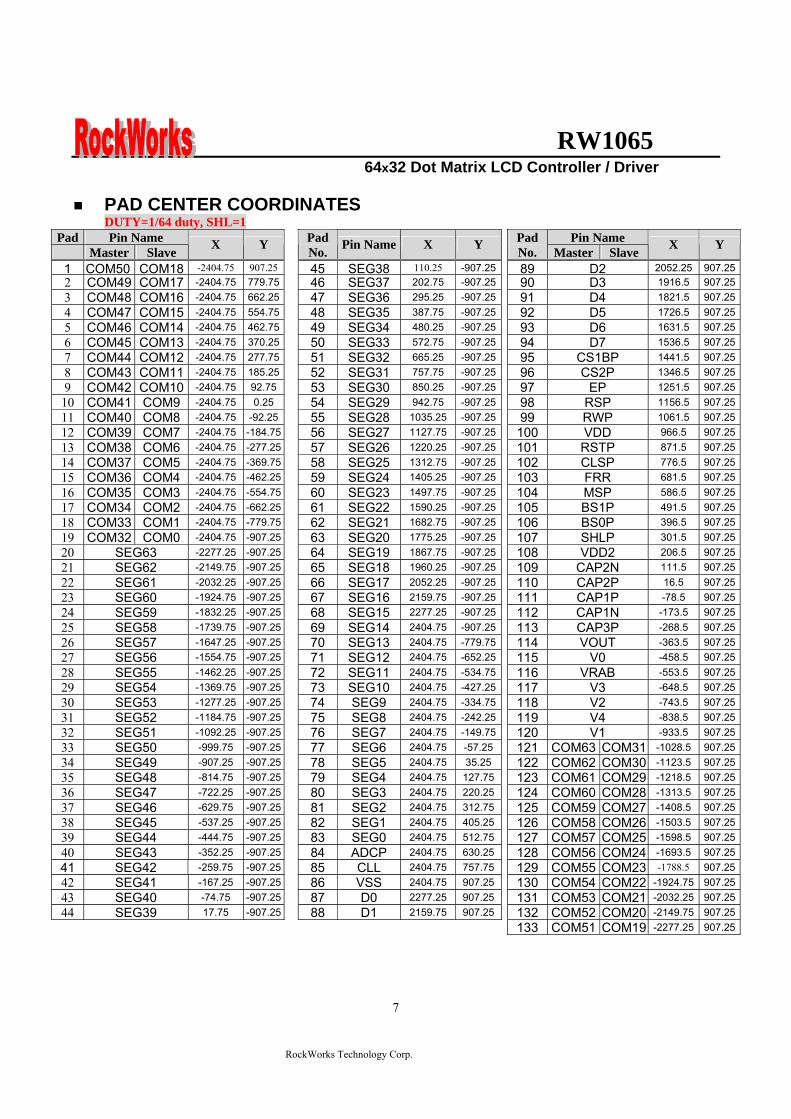
RW1065 64x32 Dot Matrix LCD Controller Driver
RockWorks Technology Corp
7
PAD CENTER COORDINATES DUTY=164 duty SHL=1
Pad Pin Name Pin Name Master Slave X Y
Pad No Pin Name X Y Pad
No Master Slave X Y
1 COM50 COM18 -240475 90725 45 SEG38 11025 -90725 89 D2 205225 907252 COM49 COM17 -240475 77975 46 SEG37 20275 -90725 90 D3 19165 907253 COM48 COM16 -240475 66225 47 SEG36 29525 -90725 91 D4 18215 907254 COM47 COM15 -240475 55475 48 SEG35 38775 -90725 92 D5 17265 907255 COM46 COM14 -240475 46275 49 SEG34 48025 -90725 93 D6 16315 907256 COM45 COM13 -240475 37025 50 SEG33 57275 -90725 94 D7 15365 907257 COM44 COM12 -240475 27775 51 SEG32 66525 -90725 95 CS1BP 14415 907258 COM43 COM11 -240475 18525 52 SEG31 75775 -90725 96 CS2P 13465 907259 COM42 COM10 -240475 9275 53 SEG30 85025 -90725 97 EP 12515 9072510 COM41 COM9 -240475 025 54 SEG29 94275 -90725 98 RSP 11565 9072511 COM40 COM8 -240475 -9225 55 SEG28 103525 -90725 99 RWP 10615 9072512 COM39 COM7 -240475 -18475 56 SEG27 112775 -90725 100 VDD 9665 9072513 COM38 COM6 -240475 -27725 57 SEG26 122025 -90725 101 RSTP 8715 9072514 COM37 COM5 -240475 -36975 58 SEG25 131275 -90725 102 CLSP 7765 9072515 COM36 COM4 -240475 -46225 59 SEG24 140525 -90725 103 FRR 6815 9072516 COM35 COM3 -240475 -55475 60 SEG23 149775 -90725 104 MSP 5865 9072517 COM34 COM2 -240475 -66225 61 SEG22 159025 -90725 105 BS1P 4915 9072518 COM33 COM1 -240475 -77975 62 SEG21 168275 -90725 106 BS0P 3965 9072519 COM32 COM0 -240475 -90725 63 SEG20 177525 -90725 107 SHLP 3015 9072520 SEG63 -227725 -90725 64 SEG19 186775 -90725 108 VDD2 2065 9072521 SEG62 -214975 -90725 65 SEG18 196025 -90725 109 CAP2N 1115 9072522 SEG61 -203225 -90725 66 SEG17 205225 -90725 110 CAP2P 165 9072523 SEG60 -192475 -90725 67 SEG16 215975 -90725 111 CAP1P -785 9072524 SEG59 -183225 -90725 68 SEG15 227725 -90725 112 CAP1N -1735 9072525 SEG58 -173975 -90725 69 SEG14 240475 -90725 113 CAP3P -2685 9072526 SEG57 -164725 -90725 70 SEG13 240475 -77975 114 VOUT -3635 9072527 SEG56 -155475 -90725 71 SEG12 240475 -65225 115 V0 -4585 9072528 SEG55 -146225 -90725 72 SEG11 240475 -53475 116 VRAB -5535 9072529 SEG54 -136975 -90725 73 SEG10 240475 -42725 117 V3 -6485 9072530 SEG53 -127725 -90725 74 SEG9 240475 -33475 118 V2 -7435 9072531 SEG52 -118475 -90725 75 SEG8 240475 -24225 119 V4 -8385 9072532 SEG51 -109225 -90725 76 SEG7 240475 -14975 120 V1 -9335 9072533 SEG50 -99975 -90725 77 SEG6 240475 -5725 121 COM63 COM31 -10285 9072534 SEG49 -90725 -90725 78 SEG5 240475 3525 122 COM62 COM30 -11235 9072535 SEG48 -81475 -90725 79 SEG4 240475 12775 123 COM61 COM29 -12185 9072536 SEG47 -72225 -90725 80 SEG3 240475 22025 124 COM60 COM28 -13135 9072537 SEG46 -62975 -90725 81 SEG2 240475 31275 125 COM59 COM27 -14085 9072538 SEG45 -53725 -90725 82 SEG1 240475 40525 126 COM58 COM26 -15035 9072539 SEG44 -44475 -90725 83 SEG0 240475 51275 127 COM57 COM25 -15985 9072540 SEG43 -35225 -90725 84 ADCP 240475 63025 128 COM56 COM24 -16935 9072541 SEG42 -25975 -90725 85 CLL 240475 75775 129 COM55 COM23 -17885 9072542 SEG41 -16725 -90725 86 VSS 240475 90725 130 COM54 COM22 -192475 9072543 SEG40 -7475 -90725 87 D0 227725 90725 131 COM53 COM21 -203225 9072544 SEG39 1775 -90725 88 D1 215975 90725 132 COM52 COM20 -214975 90725 133 COM51 COM19 -227725 90725
RW1065 64x32 Dot Matrix LCD Controller Driver
RockWorks Technology Corp
8
PAD CENTER COORDINATES DUTY=132 duty SHL=0
Pad Pin Name Pin Name Master Slave X Y
Pad No Pin Name X Y Pad
No Master Slave X Y
1 COM13 COM29 -240475 90725 45 SEG38 11025 -90725 89 D2 205225 907252 COM14 COM30 -240475 77975 46 SEG37 20275 -90725 90 D3 19165 907253 COM15 COM31 -240475 66225 47 SEG36 29525 -90725 91 D4 18215 907254 NC NC -240475 55475 48 SEG35 38775 -90725 92 D5 17265 907255 NC NC -240475 46275 49 SEG34 48025 -90725 93 D6 16315 907256 NC NC -240475 37025 50 SEG33 57275 -90725 94 D7 15365 907257 NC NC -240475 27775 51 SEG32 66525 -90725 95 CS1BP 14415 907258 NC NC -240475 18525 52 SEG31 75775 -90725 96 CS2P 13465 907259 NC NC -240475 9275 53 SEG30 85025 -90725 97 EP 12515 9072510 NC NC -240475 025 54 SEG29 94275 -90725 98 RSP 11565 9072511 NC NC -240475 -9225 55 SEG28 103525 -90725 99 RWP 10615 9072512 NC NC -240475 -18475 56 SEG27 112775 -90725 100 VDD 9665 9072513 NC NC -240475 -27725 57 SEG26 122025 -90725 101 RSTP 8715 9072514 NC NC -240475 -36975 58 SEG25 131275 -90725 102 CLSP 7765 9072515 NC NC -240475 -46225 59 SEG24 140525 -90725 103 FRR 6815 9072516 NC NC -240475 -55475 60 SEG23 149775 -90725 104 MSP 5865 9072517 NC NC -240475 -66225 61 SEG22 159025 -90725 105 BS1P 4915 9072518 NC NC -240475 -77975 62 SEG21 168275 -90725 106 BS0P 3965 9072519 NC NC -240475 -90725 63 SEG20 177525 -90725 107 SHLP 3015 9072520 SEG63 -227725 -90725 64 SEG19 186775 -90725 108 VDD2 2065 9072521 SEG62 -214975 -90725 65 SEG18 196025 -90725 109 CAP2N 1115 9072522 SEG61 -203225 -90725 66 SEG17 205225 -90725 110 CAP2P 165 9072523 SEG60 -192475 -90725 67 SEG16 215975 -90725 111 CAP1P -785 9072524 SEG59 -183225 -90725 68 SEG15 227725 -90725 112 CAP1N -1735 9072525 SEG58 -173975 -90725 69 SEG14 240475 -90725 113 CAP3P -2685 9072526 SEG57 -164725 -90725 70 SEG13 240475 -77975 114 VOUT -3635 9072527 SEG56 -155475 -90725 71 SEG12 240475 -65225 115 V0 -4585 9072528 SEG55 -146225 -90725 72 SEG11 240475 -53475 116 VRAB -5535 9072529 SEG54 -136975 -90725 73 SEG10 240475 -42725 117 V3 -6485 9072530 SEG53 -127725 -90725 74 SEG9 240475 -33475 118 V2 -7435 9072531 SEG52 -118475 -90725 75 SEG8 240475 -24225 119 V4 -8385 9072532 SEG51 -109225 -90725 76 SEG7 240475 -14975 120 V1 -9335 9072533 SEG50 -99975 -90725 77 SEG6 240475 -5725 121 COM0 COM16 -10285 9072534 SEG49 -90725 -90725 78 SEG5 240475 3525 122 COM1 COM17 -11235 9072535 SEG48 -81475 -90725 79 SEG4 240475 12775 123 COM2 COM18 -12185 9072536 SEG47 -72225 -90725 80 SEG3 240475 22025 124 COM3 COM19 -13135 9072537 SEG46 -62975 -90725 81 SEG2 240475 31275 125 COM4 COM20 -14085 9072538 SEG45 -53725 -90725 82 SEG1 240475 40525 126 COM5 COM21 -15035 9072539 SEG44 -44475 -90725 83 SEG0 240475 51275 127 COM6 COM22 -15985 9072540 SEG43 -35225 -90725 84 ADCP 240475 63025 128 COM7 COM23 -16935 9072541 SEG42 -25975 -90725 85 CLL 240475 75775 129 COM8 COM24 -17885 9072542 SEG41 -16725 -90725 86 VSS 240475 90725 130 COM9 COM25 -192475 9072543 SEG40 -7475 -90725 87 D0 227725 90725 131 COM10 COM26 -203225 9072544 SEG39 1775 -90725 88 D1 215975 90725 132 COM11 COM27 -214975 90725 133 COM12 COM28 -227725 90725
RW1065 64x32 Dot Matrix LCD Controller Driver
RockWorks Technology Corp
9
PAD CENTER COORDINATES DUTY=132 duty SHL=1
Pad Pin Name Pin Name Master Slave X Y
Pad No Pin Name X Y Pad
No Master Slave X Y
1 COM18 COM2 -240475 90725 45 SEG38 11025 -90725 89 D2 205225 907252 COM17 COM1 -240475 77975 46 SEG37 20275 -90725 90 D3 19165 907253 COM16 COM0 -240475 66225 47 SEG36 29525 -90725 91 D4 18215 907254 NC NC -240475 55475 48 SEG35 38775 -90725 92 D5 17265 907255 NC NC -240475 46275 49 SEG34 48025 -90725 93 D6 16315 907256 NC NC -240475 37025 50 SEG33 57275 -90725 94 D7 15365 907257 NC NC -240475 27775 51 SEG32 66525 -90725 95 CS1BP 14415 907258 NC NC -240475 18525 52 SEG31 75775 -90725 96 CS2P 13465 907259 NC NC -240475 9275 53 SEG30 85025 -90725 97 EP 12515 9072510 NC NC -240475 025 54 SEG29 94275 -90725 98 RSP 11565 9072511 NC NC -240475 -9225 55 SEG28 103525 -90725 99 RWP 10615 9072512 NC NC -240475 -18475 56 SEG27 112775 -90725 100 VDD 9665 9072513 NC NC -240475 -27725 57 SEG26 122025 -90725 101 RSTP 8715 9072514 NC NC -240475 -36975 58 SEG25 131275 -90725 102 CLSP 7765 9072515 NC NC -240475 -46225 59 SEG24 140525 -90725 103 FRR 6815 9072516 NC NC -240475 -55475 60 SEG23 149775 -90725 104 MSP 5865 9072517 NC NC -240475 -66225 61 SEG22 159025 -90725 105 BS1P 4915 9072518 NC NC -240475 -77975 62 SEG21 168275 -90725 106 BS0P 3965 9072519 NC NC -240475 -90725 63 SEG20 177525 -90725 107 SHLP 3015 9072520 SEG63 -227725 -90725 64 SEG19 186775 -90725 108 VDD2 2065 9072521 SEG62 -214975 -90725 65 SEG18 196025 -90725 109 CAP2N 1115 9072522 SEG61 -203225 -90725 66 SEG17 205225 -90725 110 CAP2P 165 9072523 SEG60 -192475 -90725 67 SEG16 215975 -90725 111 CAP1P -785 9072524 SEG59 -183225 -90725 68 SEG15 227725 -90725 112 CAP1N -1735 9072525 SEG58 -173975 -90725 69 SEG14 240475 -90725 113 CAP3P -2685 9072526 SEG57 -164725 -90725 70 SEG13 240475 -77975 114 VOUT -3635 9072527 SEG56 -155475 -90725 71 SEG12 240475 -65225 115 V0 -4585 9072528 SEG55 -146225 -90725 72 SEG11 240475 -53475 116 VRAB -5535 9072529 SEG54 -136975 -90725 73 SEG10 240475 -42725 117 V3 -6485 9072530 SEG53 -127725 -90725 74 SEG9 240475 -33475 118 V2 -7435 9072531 SEG52 -118475 -90725 75 SEG8 240475 -24225 119 V4 -8385 9072532 SEG51 -109225 -90725 76 SEG7 240475 -14975 120 V1 -9335 9072533 SEG50 -99975 -90725 77 SEG6 240475 -5725 121 COM31 COM15 -10285 9072534 SEG49 -90725 -90725 78 SEG5 240475 3525 122 COM30 COM14 -11235 9072535 SEG48 -81475 -90725 79 SEG4 240475 12775 123 COM29 COM13 -12185 9072536 SEG47 -72225 -90725 80 SEG3 240475 22025 124 COM28 COM12 -13135 9072537 SEG46 -62975 -90725 81 SEG2 240475 31275 125 COM27 COM11 -14085 9072538 SEG45 -53725 -90725 82 SEG1 240475 40525 126 COM26 COM10 -15035 9072539 SEG44 -44475 -90725 83 SEG0 240475 51275 127 COM25 COM9 -15985 9072540 SEG43 -35225 -90725 84 ADCP 240475 63025 128 COM24 COM8 -16935 9072541 SEG42 -25975 -90725 85 CLL 240475 75775 129 COM23 COM7 -17885 9072542 SEG41 -16725 -90725 86 VSS 240475 90725 130 COM22 COM6 -192475 9072543 SEG40 -7475 -90725 87 D0 227725 90725 131 COM21 COM5 -203225 9072544 SEG39 1775 -90725 88 D1 215975 90725 132 COM20 COM4 -214975 90725 133 COM19 COM3 -227725 90725
RW1065 64x32 Dot Matrix LCD Controller Driver
RockWorks Technology Corp
10
Pin Description
(1)Power Pins
Name IO Description
VDD - Connected to the +5V 0r +3V dc power Common to the Vcc MPU power pin
VDD2 This is the retevence power supply for the Step-up voltage circuit
VSS - 0V dc pin connected to the system ground
CAP1P~3P CAP1N~2N - Capacitor connector pin for voltage booster
V0~V4 - Multi-level power supplies for LCD driving The voltage determined for each liquid crystal cell is divided by resistance or it is converted in impedance by the op amp and supplied These voltages must satisfy the following V0 ≧ V1 ≧ V2 ≧ V3 ≧V4 ≧ VSS
(2)System Bus Connection Pins Name IO Description
D7 to D0 IO The 8-bit bidirectional data buses to be connected to the 8- or 16- bit standard MCU Data busses
RS I Usually connected to the low-order bit of the MPU address bus and used to identify the data or a command RS=0 D0 to D7 are display control data RS=1 D0 to D7 are display data
CLS I CLS=1 internal oscillator enable CLS=0 external clock operation mode
ADCP I
The pin selects the relationship between display data RAM column addresses and segment drivers ADCP=1 SEG0larrcolumn address 3FHhellipinverted ADCP=0 SEG0larrcolumn address 00Hhellipnormal
SHLP I
The pin selects the com output scan direction SHL=1 Reverse directioncom63rarrcom0 SHL=0 Normal com0rarrcom63 Both master and slave should set identical SHL value
BS1PBS0P I
Select LCD Bias 15 16 18 19 bias BS1P=0 BS0P=0 15 bias BS1P=0 BS0P=1 16 bias BS1P=1 BS0P=0 18 bias BS1P=1 BS0P=1 19 bias
RST ―
I Input low active System reset
CS1BP CS2P I Input When CS1BP = 0 and CS2P = 1 the chip select become active
E I For 68-series MPU Input Active high
Used as an enable clock input of the 68-series MPU
RW I For 68-series MPU Input
Used as an input pin of read control signals (if RW is high) or write control signals signals (if low)
RW1065 64x32 Dot Matrix LCD Controller Driver
RockWorks Technology Corp
11
(3)LCD Driver Circuit Signals
Name IO Description
CLL IO
Inputoutput IO selection
MS = ldquoHrdquo amp CLS = ldquoHrdquo Output MS = ldquoLrdquo amp CLS = ldquoHrdquo Input MS = ldquoXrdquo amp CLS = ldquoLrdquo Input
This is a display data latch signal to count up the line counter and common counterat each signal falling and rising edges
SEGn O Output A single level of V0 V2 V3 and VSS is selected by the combination of display RAM contents and FR signal
COMn O Output The output pin for LCD common (row) driving A single level of V0 V1 V4 and VSS is selected by the combination of common counter output and FR signal The slave LSI has the reverse common output scan sequence than the master LSI
FRR IO
Inputoutput This is the liquid crystal alternating current signal IO terminal lO selection
MS = ldquoHrdquoOutput MS = ldquoLrdquoInput
VRAB I Provides the voltage between V0 and VSS through a resistive voltage divider
MS I
Input The master or slave LSI operation select pin for the RW1065
MS OperatingMode FR CL V0~V4 Power
SupplyInternal
OSC COMMON
Output SEG
output
High Master Output See CLS On On See
CLS COM0-31 SEG0-63
Low Slave Input Input Off Off Off COM32-63
SEG64-127
RW1065 64x32 Dot Matrix LCD Controller Driver
RockWorks Technology Corp
12
DESCRIPTION OF FUNCTIONS
The Parallel Interface (6800 series MPU)
Shared 6800 Series
RS RW Function
1 1 Reads the display data
1 0 Writes the display data
0 1 Status read
0 0 Write control data (command)
The Chip Select The RW1065 Series chips have two chip select terminals CS1
―BP and CS2P
When the chip select is inactive D0 to D7 enter a high impedance state and the RS E and RW inputs are inactive
The Accessing the Display Data RAM and the Internal Registers Data transfer at a higher speed is ensured since the MPU is required to satisfy the cycle time (tCYC) requirement alone in accessing the RW1065 Series Wait time may not be considered And in the RW1065 Series chips each time data is sent from the MPU a type of pipeline process between LSIs is performed through the bus holder attached to the internal data bus Internal data bus For example when the MPU writes data to the display data RAM once the data is stored in the bus holder then it is written to the display data RAM before the next data write cycle Moreover when the MPU reads the display data RAM
the first data read cycle (dummy) stores the read data in the bus holder and then the data is read from the bus holder to the system bus at the next data read cycle There is a certain restriction in the read sequence of the display data RAM Please be advised that data of the specified address is not generated by the read instruction issued immediately after the address setup This data is generated in data read of the second time Thus a dummy read is required whenever the address setup or write cycle operation is conducted This relationship is shown in Figure 2
RW1065 64x32 Dot Matrix LCD Controller Driver
RockWorks Technology Corp
13
E
Fig 2b read timing
E
RW
Fig 2a write timing (RW=rdquoLrdquo)
RS
RS
RW1065 64x32 Dot Matrix LCD Controller Driver
RockWorks Technology Corp
14
Display Data RAM The display data RAM is a RAM that stores the dot data for the display It has a 64 (8 page x 8 bit) x 64 bit structure It is possible to access the desired bit by specifying the page address and the column addressBecause as is shown in Figure 3 the D7 to D0 display data from the MPU corresponds to the liquid crystal display common direction there are few constraints at the time of display data transfer when multiple RW1065 series chips are used
thus and display structures can be created easily and with a high degree of freedom Moreover reading from and writing to the display RAM from the MPU side is performed through the IO buffer which is an independent operation from signal reading for the liquid crystal driver Consequently even if the display data RAM is accessed asynchronously during liquid crystal display it will not cause adverse effects on the display (such as flickering)
0
1
0
0
1
1
0
0
1
0
1
0
0
1
0
1
0
0
1
0
0
0
0
0
0
D0
D1
D2
D3
D4
-
Display data RAM Liquid crystal display
COM0
COM1
COM2
COM3
COM4
-
Figure3
The Page Address Circuit As shown in Figure 4 page address of the display data RAM is specified through the Page Address Set Command The page address must be specified again when changing pages to perform access
The Column Address As is shown in Table 4 the display data RAM column address is specified by the Column Address Set command The specified column address is incremented (+1) with each display data readwrite command This allows the MPU display data to be accessed continuously Moreover the increment of column addresses stops with 3FH Because the column address is independent of the page address when moving for example from page 0 column 3FH to page 1
column 00H it is necessary to respecify both the page address and the column address Furthermore as is shown in Table 4 the ADC command (segment driver direction select command) can be used to reverse the relationship between the display data RAM column address and the segment output Because of this the constraints on the IC layout when the LCD module is assembled can be minimized
Table 4 SEG Output
ADC set SEG0 SEG 63
ADC(D0)=0 0 rarr Column Address rarr 63 ADC(D0)=1 63 larr Column Address larr 0
RW1065 64x32 Dot Matrix LCD Controller Driver
RockWorks Technology Corp
15
Figure 4
Page Address D3 D2 D1 D0
DataSE
G0
SEG
1
SEG
2
SEG
3
SEG
4
SEG
5
SEG
6
SEG
7
SEG
8
helliphelliphelliphellip
SEG
55
SEG
56
SEG
57
SEG
58
SEG
59
SEG
60
SEG
61
SEG
62
SEG
63 SEG
COM
D0 COM0
D1 COM1
D2 COM2
D3 COM3
D4 COM4
D5 COM5
D6 COM6
0 0 0 0
D7
Page 0
COM7
D0 COM8
D1 COM9
D2 COM10
D3 COM11
D4 COM12
D5 COM13
D6 COM14
0 0 0 1
D7
Page 1
COM15
D0 COM16
D1 COM17
D2 COM18
D3 COM19
D4 COM20
D5 COM21
D6 COM22
0 0 1 0
D7
Page 2
COM23
D0 COM24
D1 COM25
D2 COM26
D3 COM27
D4 COM28
D5 COM29
D6 COM30
0 0 1 1
D7
Page 3
COM31
ADC=0 00
01
02
03
04
05
06
07
08
helliphelliphelliphellip 55
56
57
58
59
60
61
62
63
COLUMN ADC=1 63
62
61
60
59
58
57
56
55
helliphelliphelliphellip 08
07
06
05
04
03
02
01
00
RW1065 64x32 Dot Matrix LCD Controller Driver
RockWorks Technology Corp
16
Common Timing Generator Circuit Display Data Latch Circuit Generates common timing signals and FR frame signals from the CL basic clock The 132 or 164 duty (for RW1065) can be selected by the Duty Select command The 132 and 164 duties are provided by two chips consisting of the master and slave chips in the common multi-chip mode
This latch stores one line of display data for use by the LCD driver interface circuitry The output of this latch is controlled by the Display ONOFF
132 duty
164 duty
SHL=0
SHL=1
SHL=0
SHL=1
RW1065 64x32 Dot Matrix LCD Controller Driver
RockWorks Technology Corp
17
Display Timing Generator Circuit
The display timing generator circuit generates the timing signal to the line address circuit and the display data latch circuit using the display clock The display data is latched into the display data latch circuit synchronized with the display clock and is output to the data driver output terminal Reading to the display data liquid crystal driver circuits is completely independent of accesses to the display data RAM by the MPU Consequently even if the display data
RAM is accessed asynchronously during liquid crystal display there is absolutely no adverse effect (such asflickering) on the display Moreover the display timing generator circuit generates the common timing and the liquid crystal alternating current signal (FR) from the display clock It generates a drive wave form using a 2 frame alternating current drive method as is shown in Figure 5 for the liquid crystal drive circuit
Two-frame alternating current drive waveform
Figure 5
When multiple RW1065 Series chips are used the slave chip must be supplied the display timing signals(FR CL) from the master chip
Table 5 shows the status of the FR and CL signals
Table 5 Operating Mode FR CL
Master (MS = ldquoHrdquo) The internal oscillator circuit is enabled (CLS = ldquoHrdquo) The internal oscillator circuit is disabled (CLS = ldquoLrdquo)
Output Output
Output Input
Slave (MS = ldquoLrdquo) The internal oscillator circuit is enabled (CLS = ldquoHrdquo) The internal oscillator circuit is disabled (CLS = ldquoLrdquo)
Input Input
Input Input
RW1065 64x32 Dot Matrix LCD Controller Driver
RockWorks Technology Corp
18
The Liquid Crystal Driver Circuits
These are a 64-channel (RW1065) that generate four voltage levels for driving the liquid crystal The combination of the display data the COM scan signal and the FR signal
produces the liquid crystal drive voltage output Figure 6 shows examples of the SEG and COM output waveform
Figure 6
RW1065 64x32 Dot Matrix LCD Controller Driver
RockWorks Technology Corp
19
The Power Supply Circuit
The power supply circuits are low-power consumption power supply circuits that generate the voltage levels required for the liquid crystal drivers They comprise Booster circuits and voltage follower circuits They are only enabled in master operation The power supply circuits can turn on automatically after power on
Consequently it is possible to make an external power supply and the internal power supply function somewhat in parallel
The Liquid Crystal Voltage Generator Circuit The V0 voltage is produced by a resistive voltage divider outside the IC through VRAB pin and can be produced at the V1 V2 V3 and V4 voltage levels required for liquid crystal driving Moreover when the voltage follower changes the impedance it provides V1 V2 V3 and V4 to the liquid crystal drive circuit 15 bias or 16 bias or 18 bias or 19 bias for RW1065 can be selected by BS0 and BS1 pins V0-Vss maximum voltage is 15V Vout-Vss maximum voltage is 17V If VDD lt 35V it can use the Booster circuit 2x3x4xThe booster voltage can follow the spec condition (Vout-Vss ≦ 17V max voltage) if VDD gt35V only use the 2X3X booster circuit that can ensure the V0-Vss voltage ≦ 15V If use the VDD voltage 5V and 4X booster itrsquos over the spec operation condition To turn on built-in power (boosterfollower) must waiting 200mS to display on for boosterfollower stable Therefore power off must follower ldquopower off sequencerdquo too
Power on Display off
Power off
Power off sequence
Wait time gt200mS
Display on
Power on sequence
RW1065 64x32 Dot Matrix LCD Controller Driver
RockWorks Technology Corp
20
The Reset Circuit
When the RTP input comes to the ldquoLrdquo level these LSIs return to the default state Their default states are as follows 1 Display OFF 2 Display all point on is select to normal 3 Display normalreverse is select to normal 4 164 duty is selected 5 Read modify write OFF 6 Column address set to Address 0 7 Page address set to Page 0 8 Start line set to first line 9 Frame frequency set to default 10 Power save mode released 11 Ext set to ldquo0rdquo When the power is turned on the IC internal state becomes unstable and it is necessary to initialize it using the RSTP terminal After the initialization each input terminal should be controlled normally While RSTP is ldquoLrdquo the oscillator works but the display timing generator stops and the CL FR terminals are fixed to ldquoHrdquo The terminals D0 to D7 are not affected
RW1065 64x32 Dot Matrix LCD Controller Driver
RockWorks Technology Corp
21
TABLE OF RW1065 INSTRUCTIONS
Instruction code Instruction RS RW DB7 DB6 DB5 DB4 DB3 DB2 DB1 DB0 Description
EXT=0 or 1
MODE SET 0 0 0 0 0 0 1 1 0 EXT Set EXT mode
Instruction code Instruction RS RW DB7 DB6 DB5 DB4 DB3 DB2 DB1 DB0 Description
EXT=0 Display ONOFF 0 0 0 0 1 1 1 1 1 D D=0Display OFF
D=1Display ONSet page address 0 0 1 0 1 1 1 P2 P1 P0 Set page address
Set column address 0 0 0 1 Y5 Y4 Y3 Y2 Y1 Y0 Set column
address MSB
Read Status 0 1 BUSY 0 ON OFF RESET 0 0 0 0 Read register
status Write display
data 1 0 Write data Write data into DDRAM
Read display data 1 1 Read data Read data from
DDRAM Set initial
display line register
0 0 1 1 S5 S4 S3 S2 S1 S0 Specify the initial
display line to realize vertical scrolling
Instruction code Instruction RS RW DB7 DB6 DB5 DB4 DB3 DB2 DB1 DB0 Description
EXT=1
NOP 0 0 0 0 0 0 0 0 0 0 no operation
Set modiy-read 0 0 0 0 0 0 1 0 0 0 Set modiy-read
mode
END 0 0 0 0 0 0 1 1 1 0 release modiy-read mode
Set power save mode 0 0 0 0 0 0 0 0 1 PSAVE P=0 normal mode
P=1 sleep mode
0 0 0 0 0 1 0 1 Display
COMMAND (double
command)
0 0 FRSEL
0 0 0 0 REV ALLON DUTY
DUTY=1 64 duty DUTY=0 32 duty ALLON=1display all on ALLON=0display
normal REV=1display reverse REV=0display normal FRSEL=1FR frequency double default FRSEL=0FR frequency default
RW1065 64x32 Dot Matrix LCD Controller Driver
RockWorks Technology Corp
22
Command Description
See the Table of RW1065 instructions The RW1065 series identifies a data bus using a combination of RS E and RW signals As the MPU translates a command in the internal timing only (independent from the external clock) its speed is very high The busy check is usually not required
Display ONOFF
EXT RS RW D7 D6 D5 D4 D3 D2 D1 D0
0 0 0 0 0 1 1 1 1 1 D
This command turns the display on and off D=1 Display ON D=0 Display OFF(default)
Set page Address This command specifies the page address that corresponds to the low address of the display data RAM when it is accessed by the MPU Any bit of the display data RAM can be accessed when its page address and column address are specified The display status is not changed even when the page address is changed
EXT RS RW D7 D6 D5 D4 D3 D2 D1 D0
0 0 0 1 0 1 1 1 A2 A1 A0
This command loads the page address register
A2 A1 A0 Page
0 0 0 0 (default)
0 0 1 1 0 1 0 2 0 1 1 3 1 0 0 4 1 0 1 5 1 1 0 6 1 1 1 7
Page mapping see Figure 4
RW1065 64x32 Dot Matrix LCD Controller Driver
RockWorks Technology Corp
23
Set Column Address This command specifies a column address of the display data RAM When the display data RAM is accessed by the MPU continuously the column address is incremented by I each time it is accessed from the set address Therefore the MPU can access to data continuously The column address stops to be incremented at address 63 and the page address is not changed continuously
EXT RS RW D7 D6 D5 D4 D3 D2 D1 D0
0 0 0 0 1 A5 A4 A3 A2 A1 A0
A5 A4 A3 A2 A1 A0 Column Address0 0 0 0 0 0 0(default) 0 0 0 0 0 1 1
1 1 1 1 1 1 63
Read Status
EXT RS RW D7 D6 D5 D4 D3 D2 D1 D0
0 0 1 BUSY 0 ON OFF RESET 0 0 0 0
The BUSY Flag bit indicates that RW 1065 is operating or no operating
BUSY=1 Operation BUSY=0 Ready
The ONOFF bit indicates the current status of the display It is the inverse of the polarity of the display ONOFF command ONOFF=1 Display OFF ONOFF=0 Display ON The RESET bit indicates whether the driver is executing a hardware or software reset or if it is in normal operating mode RESET=1 Currently executing reset command RESET=0 Normal operation
RW1065 64x32 Dot Matrix LCD Controller Driver
RockWorks Technology Corp
24
Write Display Data
EXT RS RW D7 D6 D5 D4 D3 D2 D1 D0
0 1 0 Write data
Writes 8-bits of data into the display data RAM at a location specified by the contents of the column address and page address registers and then increments the column address register by one
Read Display Data
EXT RS RW D7 D6 D5 D4 D3 D2 D1 D0
0 1 1 Read data
Reads 8-bits of data from the data IO latch updates the contents of the IO latch with display data from the display data RAM location specified by the contents of the column address and page address registers and then increments the column address register After loading a new address into the column address register one dummy read is required before valid data is obtained
Set initial display line register
EXT RS RW D7 D6 D5 D4 D3 D2 D1 D0
0 0 0 1 1 S5 S4 S3 S2 S1 S0
Loads the RAM line address of the initial display line COM 0 into the initial display line register The RAM display data becomes the top line of the LCD screen It is followed by the higher number lines in ascending order corresponding to the duty cycle The screen can be scrolled using this command by incrementing the line address(default value=rdquo00Hrdquo)
RW1065 64x32 Dot Matrix LCD Controller Driver
RockWorks Technology Corp
25
Read-Modify-Write
EXT RS RW D7 D6 D5 D4 D3 D2 D1 D0
1 0 0 0 0 0 0 1 0 0 0
This command defeats column address register auto-increment after data reads The current contents of the column Address register are saved The mode remains active until an End command is received When the End command is entered the column address is returned to the one used during input of Read-Modify-Write Command This function can reduce the load of MPU when data change is repeated as a specific display area Any command other than Data Read or Write can be used in the Read-Modify-Write mode However the Column Address Set command cannot be used
End
EXT RS RW D7 D6 D5 D4 D3 D2 D1 D0
1 0 0 0 0 0 0 1 1 1 0
This command cancels read-modify-write mode and restores the contents of the column address register to their value prior to the receipt of the Read-Modify-Write command
N N+1 N+2 N+3 N+m N
Read -modify-write mode set End
Returm
Column address
Set page address
Set column address
Read-modify-write
Dummy read
Read data
Write data
End
CompletedNo
Yes
RW1065 64x32 Dot Matrix LCD Controller Driver
RockWorks Technology Corp
26
Set power save mode
EXT RS RW D7 D6 D5 D4 D3 D2 D1 D0
1 0 0 0 0 0 0 0 0 1 PSAVE
When power save mode is entered thus greatly reducing power consumption In the power save mode the display data is saved as is the operating mode that was in effect before the power saver mode was initiated and the MPU is still able to access the display data RAM PSAVE=1 Sleep mode PSAVE=0 Normal mode Sleep mode This stops all operations in the LCD display system and as long as there are no accesses from the MPU the consumption current is reduced to a value near the static current The internal modes during sleep mode are as follows 1 The oscillator circuit and the LCD power supply circuit are halted 2 All liquid crystal drive circuits are halted and the segment and common drive outputs output a Vss level
Display command double command
EXT RS RW D7 D6 D5 D4 D3 D2 D1 D0
1 0 0 0 0 0 0 0 1 0 1
1 0 0 FRSEL 0 0 0 0 REV ALLON DUTY
Display NormalReverse set REV=1 Reverse REV=0 Normal(default) Display All Point ONOFF ALLON=1 All display points ON ALLON=0 Normal(default) Select Duty Duty=1 164 duty cycle(default) Duty=0 132 duty cycle FRAME FREQUENCY Select FRSEL=1 Double FRSEL=0 (default)
RW1065 64x32 Dot Matrix LCD Controller Driver
RockWorks Technology Corp
27
Hardware Pin Set
Select ADC by ADC Pin The pin selects the relationship between display data RAM column addresses and segment drivers ADC=1 SEG0larrcolumn address 3FHhellipinverted ADC=0 SEG0larrcolumn address 00Hhellipnormal(default) This command is provided to reduce restrictions on the placement of driver ICs and routing of traces during printed circuit Board design See Figure 4 for a table of segments and column addresses for the two values of D
Select SHL by SHL Pin The pin selects the com output scan direction SHL=1 Reverse directioncom63rarrcom0 SHL=0 Normal com0rarrcom63 Both master and slave should set identical SHL value
Select LCD Bias by BS0 BS1 Pin
BS1 BS0 Bias 0 0 15 bias 0 1 16 bias 1 0 18 bias 1 1 19 bias
RW1065 64x32 Dot Matrix LCD Controller Driver
RockWorks Technology Corp
28
When an External Resistance is Used The liquid crystal power supply voltage V0 is set by adding resistors Rarsquo and Rbrsquo between VDD and VR and between VR and V0 respectively
RW1065
RW1065 64x32 Dot Matrix LCD Controller Driver
RockWorks Technology Corp
29
The set voltage circuits
Using the step-up voltage circuits equipped within the RW1065 chips it is possible to produce a 2X 3X 4X step-up voltage levels 2X step-up
To produce voltage level in the positive direction at the Vout terminal that is 2 times the voltage difference between VSS and VDD2 Please configure set voltage circuits like this Place a 1uF~22uF capacitor between CAP1N and CAP1P Place a 1uF~22uF capacitor between VSS and VOUT Short CAP2P CAP3P and VOUT Leave CAP2N open 3X step-up
To produce voltage level in the positive direction at the Vout terminal that is 3 times the voltage difference between VSS and VDD2 Please configure set voltage circuits like this Place a 1uF~22uF capacitor between CAP1N and CAP1P Place a 1uF~22uF capacitor between VSS and VOUT Place a 1uF~22uF capacitor and 100 ohms resistor between CAP2N and CAP2P Short CAP3P and Vout 4X step-up
To produce voltage level in the positive direction at the Vout terminal that is 4 times the voltage difference between VSS and VDD2 Please configure set voltage circuits like this Place a 1uF~22uF capacitor between CAP1N and CAP1P Place a 1uF~22uF capacitor between VSS and VOUT Place a 1uF~22uF capacitor and 100 ohms resistor between CAP2N and CAP2P Place a 1uF~22uF capacitor and 100 ohms resistor between CAP1N and CAP3P
RW1065 64x32 Dot Matrix LCD Controller Driver
RockWorks Technology Corp
30
ABSOLUTE MAXIMUM RATINGS Characteristics Symbol Value Unit
Power supply voltage VDD -03 to +70 V
LCD driver voltage Vout 0 to +17 V
Input voltage VIN -03 to VDD+03 V
Operating temperature TA -40 to +85
Storage temperature TSTO -55 to +125
DC CHARACTERISTICS
Rating Item Symbol Condition Min Typ Max Unit ApplicablePin
Operating Voltage VDD - 27 30 55 V VDD1
Step up output voltage Vout (Relative to VDD) 0 - 17 V Vout
Voltage follower circuit operating Voltage V0 (Relative to VDD) 0 - 15 V V0
V0 accuracy V0 - 0 - 15 V0
High-level Input Voltage Low-level Input Voltage
VIHC VILC - 07 VDD
Vss - VDD 09 V 2
High-level Output Voltage Low-level Output Voltage
VOHC VOLC
IOH = ndash05 mA IOL = 05 mA
08VDD Vss - VDD
02 VDD V 3
Input leakage current ILI VIN = VDD or VSS -1 - 2 uA 4
Output leakage current ILO - -1 1 uA 5
Liquid Crystal Driver ON Resistance RON
Ta= 25degC(Relative To VDD)
V0 =15 V - 16 20 KΩ SEGn COMn 6
Internal Oscillator fOSC 2286 254 2794 Oscillator
Frequency External Input RECOMMAND fCL
Ta = 25degC 132Duty 2286 254 2794
kHz CL
Internal Oscillator fOSC 45 5 55 Oscillator
Frequency External Input RECOMMAND fCL
Ta = 25degC 164Duty 45 5 55
kHz CL
bullDynamic Consumption Current During Display with the Internal Power Supply OFF Current consumed by total ICs when an external power supply is used
Unless otherwise specified Vss=0V VDD=30V
RW1065 64x32 Dot Matrix LCD Controller Driver
RockWorks Technology Corp
31
Display Pattern OFF
Ta = 25degC Vout=17V Rating Item Symbol Condition Min Typ Max Unit Notes
VDD=30 V V0-Vss=8V - 10 15 RW1065 IDD VDD=50 V V0-Vss=8V - 35 45
microA 7
Display Pattern Checker
Ta = 25degC Vout=17V Rating Item Symbol Condition Min Typ Max Unit Notes
VDD=30 V V0-Vss=8V - 15 20 RW1065 IDD VDD=50 V V0-Vss=8V - 40 50
microA 7
Display Pattern OFF
Ta = 25degC Vout=17V Rating Item Symbol Condition Min Typ Max Unit Notes
VDD=30 V V0-Vss=8V - 15 20 RW1065 IDD VDD=50 V V0-Vss=8V - 40 50
microA 7
Display pattern Checker
Ta = 25degC Vout=17V Rating Item Symbol Condition Min Typ Max Unit Notes
VDD=30 V V0-Vss=8V - 65 80 RW1065 IDD VDD=50 V V0-Vss=8V - 130 150
microA 7
bull Consumption Current at Time of Power Saver Mode VSS = 0 V VDD = 30 V plusmn 10
Rating Item Symbol Condition Min Typ Max Unit Notes
Sleep mode IDD - - 5 10 microA -
References for items market with 1 While a broad range of operating voltages is guaranteed performance cannot be guaranteed if there are sudden fluctuations to the
voltage while the MPU is being accessed 2 The RS D0 to D5 D6 D7 E RW CS1BP CS2P CLS CL FR MS and RST
― terminals
3 The D0 to D7 FR and CL terminals 4 The RS E RW CS1BP CS2P CLS MS and RST
― terminals
5 Applies when the D0 to D5 D6 D7 CL and FR terminals are in a high impedance state 6 These are the resistance values for when a 01 V voltage is applied between the output terminals SEGn or COMn and
the various power supply terminals (V1 V2 V3 and V4) These are specified for the operating voltage (3) range RON = 01 V ∆I (Where ∆I is the current that flows when 01 V is applied while the power supply is ON)
7 It indicates the current consumed on ICs alone when the internal oscillator circuit and display are turned on Does not include the current due to the LCD panel capacity and wiring capacity Applicable only when there is no access from the MPU
RW1065 64x32 Dot Matrix LCD Controller Driver
RockWorks Technology Corp
32
TIMING CHARACTERISTICS
68 Interface
(Ta=-40 to 85 degC) VDD=27 to 45V
Rating VDD=45 to 55V
Rating Item Signal Symbol ConditionMin Max Min Max
Units
Address hold time RS tAH6 0 mdash 0 mdash Address setup time RS tAW6
mdash 0 mdash 0 mdash
ns
System cycle time RS tCYC6 mdash 900 mdash 800 mdash ns Data setup time D0 to D7 tDS6 100 mdash 100 mdash Data hold time D0 to D7 tDH6
mdash 0 mdash 0 mdash
ns
Access time D0 to D7 tACC6 mdash 350 mdash 250
Output disable time D0 to D7 tOH6 CL = 100 pF
mdash 300 mdash 200 ns
Read tEWHR 360 mdash 300 mdash Enable H pulse time
WriteE
tEWHW mdash
360 mdash 300 mdash ns
Read tEWLR 450 mdash 400 mdash Enable L pulse time
WriteE
tEWLW mdash
450 mdash 400 mdash ns
1 All timing is specified using 20 and 80 of VDD as the reference 2 tEWLW and tEWLR are specified as the overlap between CS1BP being ldquoLrdquo (CS2P = ldquoHrdquo) and E
RW1065 64x32 Dot Matrix LCD Controller Driver
RockWorks Technology Corp
33
Reset Timing
Rating Item Signal Symbol Condition
Min Typ Max Units
Reset time mdash tR mdash mdash - 2 micros
Reset ldquoLrdquo pulse width RST tRW mdash 2 - mdash micros
1 When double chip was be used then the duty set command must be set between the tR
RW1065 64x32 Dot Matrix LCD Controller Driver
RockWorks Technology Corp
34
IO PAD CONFIGURATION
RW1065 64x32 Dot Matrix LCD Controller Driver
RockWorks Technology Corp
35
THE MPU INTERFACE (REFERENCE EXAMPLES) The RW1065 Series can be connected to 6800 Series MPUs The display area can be enlarged by using multiple RW1065 Series chips When this is done the chip select signal can be used to select the individual ICs to access
6800 Series MPUs
RW
106
5
RW1065 64x32 Dot Matrix LCD Controller Driver
RockWorks Technology Corp
36
When using external multi-level power supply for LCD driving (REFERENCE EXAMPLE)
Using a resistor divider can provide RW1065 external multi-level power supply for LCD driving
The circuit below shows a resistor divider network which can bias V0 V1 V2 V3 and V4 externally
RW1065 64x32 Dot Matrix LCD Controller Driver
RockWorks Technology Corp
37
bullWhen V0 V1 V2 V3 and V4 are biased by external power supply analog section of RW1065 should be turn off by software during LCD initialization The example in below shows the sequence to turn off analog section when external bias is used Begin of LCD initialization 1 Reset RW1065 2 SET EXT=1 (mode instruction)
RS RW DB7 DB6 DB5 DB4 DB3 DB2 DB1 DB00 0 0 0 0 0 1 1 0 1
3 SET Display Command (double command)
RS RW DB7 DB6 DB5 DB4 DB3 DB2 DB1 DB00 0 0 0 0 0 0 1 0 1 0 0 0 0 1 1 0 0 0 1
4 SET EXT=1 (mode instruction)
RS RW DB7 DB6 DB5 DB4 DB3 DB2 DB1 DB00 0 0 0 0 0 1 1 0 0
End of LCD initialization
bullBecause pins can not set LCD bias when external power supplies are used for LCD driving the bias can be set by an appropriate configuration for a resistor voltage divider networks The example is shown below
VSS
R
R
NR
R
R
RV1
RV2
RV3
RV4
V0
Bias Network Circuit Concept 15 Bias N=1 total = 5R 16 Bias N=2 total =6R 18 Bias N=4 total =8R 19 Bias N=5 total = 9R
RW1065 64x32 Dot Matrix LCD Controller Driver
RockWorks Technology Corp
38
Single chip solution for RW1065 application (REFERENCE EXAMPLE)
For a 64x32 application the duty cycle of LCD panel is 164 and the display duty of RW1065 should be set to 164 The display duty cycle can be selected by the DUTY bit in display command The diagram for 64x32 application is shown below
64 SEGx32COM LCD Panel
164 duty cycle
RW1065 DUTY=1
COM1~33
SEG1~65
RW1065 64x32 Dot Matrix LCD Controller Driver
RockWorks Technology Corp
39
Using an adjustable resistor on the main board to adjust the contrast of liquid crystal display (REFERENCE EXAMPLE)
The schematic shows an adjustable resistor on main board that can adjust voltage level of V0
RW1065 64x32 Dot Matrix LCD Controller Driver
RockWorks Technology Corp
40
Package information (Please pay close attention to the information in this section Do not hesitate to consult with our sale representative if you have any question or concern)
In order to make better bonding yield for RW1065 please follow the tips and recommendations in this section In this section few tips about COB footprint style PCB layout and wire bonding will be discussed
The drawing in below shows the PCB footprint style which we recommend for RW1065 Pads array in
curve shape is easier for Al wire bonding Besides that a real size COB footprint for RW1065 is also shown in below RW1065 COB footprint is also available in powerpcb or protel format for design reference purpose
The ratio is 11
RW1065 64x32 Dot Matrix LCD Controller Driver
RockWorks Technology Corp
41
During COB footprint design there have some tips about footprint that the PCB designer should know The angle between bonding wire and vertical line should less than 45 Otherwise the wire shorts would become very easy to happen at fours corners of the chip
The angle between bonding wire and vertical line could be reduced by expanding the distance between pads array and the chip In addition reducing length in horizon direction of pads array could minimize the angle between bonding wire and vertical line The picture in below will help to illustrate this concept From the experiences COB footprint style affects the bonding yield
Bad Wires are too close to each other
The angle between bonding wire and vertical line is greater than 45
The angle between bonding wire and vertical line is less than 45
Wires are not too close to each other
Reducing length in horizon direction of pads array could minimize the angle between bonding wire and vertical line
The angle between bonding wire and vertical line could be reduced by expanding the distance between pads array and the chip
RW1065 64x32 Dot Matrix LCD Controller Driver
RockWorks Technology Corp
42
If the gap between pads of COB footprint is filled with solder mask coating it is difficult to bond Al wire to
the pads The top solder masks layer that overlap COB footprint area should be removed
Please use 1 mils diameter Al wire for RW1065 wire bonding
1 2 3 4 5 6
A
B
C
D
654321
D
C
B
A
Title
Number RevisionSize
C
Date 29-Aug-2007 Sheet of File D公司資料99seMyDesignddb Drawn By
RW1065
COM131
COM142
COM153
COM164
COM175
COM186
COM197
COM208
COM219
COM2210
COM2311
COM2412
COM2513
COM2614
COM2715
COM2816
COM2917
COM3018
COM3119
SEG
6320
SEG
6221
SEG
6122
SEG
6023
SEG
5924
SEG
5825
SEG
5726
SEG
5627
SEG
5528
SEG
5429
SEG
5330
SEG
5231
SEG
5132
SEG
5033
SEG
4934
SEG
4835
SEG
4736
SEG
4637
SEG
4538
SEG
4439
SEG
4340
SEG
4241
SEG
4142
SEG
4043
SEG
3944
SEG
3845
SEG
3746
SEG
3647
SEG
3548
SEG
3449
SEG
3350
SEG
3251
SEG
3152
SEG
3053
SEG
2954
SEG
2855
SEG
2756
SEG
2657
SEG
2558
SEG
2459
SEG
2360
SEG
2261
SEG
2162
SEG
2063
SEG
1964
SEG
1865
SEG
1766
SEG
1667
SEG
1568
SEG
1469
SEG13 70SEG12 71SEG11 72SEG10 73SEG9 74SEG8 75SEG7 76SEG6 77SEG5 78SEG4 79SEG3 80SEG2 81SEG1 82SEG0 83ADCP 84CLL 85
VSS
86D
087
D1
88D
289
D3
90D
491
D5
92D
693
D7
94C
S1B
P95
CS2
P96
ERD
P97
AO
P(R
S)98
RW
RP
99V
DD
100
RST
P10
1C
LSP
102
FRR
103
MSP
104
BS1
P10
5B
S0P
106
SHLP
107
VD
D2
108
CA
P2N
109
CA
P2P
110
CA
P1P
111
CA
P1N
112
CA
P3P
113
VO
UT
114
V0
115
VR
AB
116
V3
117
V2
118
V4
119
V1
120
CO
M0
121
CO
M1
122
CO
M2
123
CO
M3
124
CO
M4
125
CO
M5
126
CO
M6
127
CO
M7
128
CO
M8
129
CO
M9
130
CO
M10
131
CO
M11
132
CO
M12
133
4897x1902 um
IC1
RW1065
C9CAPR4
100R0603
R30R0603
C8
CAP
C7
CAP
R2
100R0603
R1
0R0603C6 22uf
R50R
R6300R
R7RES1
R8NC R9
100R0603
VDD
R10
NC
R11
100R0603
R12
100R0603
R13
NC
R14
100R0603
R15
NC
VDD
D0
D1
D2
D3
D4
D5
D6
D7
DB[07]
VDDC5
01uf0603
VD
D
CS2
P
123456789
1011121314151617181920
J1
CON20
C1201uf0603
R3951K0603
VDD
CAP Value1UF~22UF
2XPut C6C8 Short R1R3Open R2R4C7C93XPut C6C8C9 R4Short R1Open R2R3C74XOpen R1R3
BS0 BS1 Bias0 0
0 1
1 0
11
15 bias
16 bias
18 bias
19 bias
ADC=0 SEG0lt~column address 00Hnormal(default) ADC=1 SEG0lt~column address 3FHinverted
SHL=0 Normal COM0~gtCOM63(default)SHL=1 Reverse direction COM63~gtCOM0
R16100R0603
LCD PANEL 64X32RockWorks
RW1065 64X32
COM0-31 SEG0-63SHL=0 ADC=0
SHL=1COM31-0
ADC=1SEG63-0
if use single chip for 32 command displaythe display command must select 164 dutyDisplay panel must select 164 duty type
VO
UT
C3P
C1N
C1P
C2P
C2N
VDD2
ADC
SHL
BS0
BS1
CLLADC
V1
V2
V3
V4
VR
AB
V0
VO
UT
C3P
C1N
C1P
C2P
C2N
VD
D2
SHL
BS0
BS1
FRR
RST
P
RW
RS
E CS1
B
CS1
V0RSRWED0D1D2D3D4D5D6D7
RSTPAK
C4
22uf
RBRES1
RA1RES1
C2
22uf
C1
22uf
C3
22uf
C0
22uf
R20
100k0603
R21
100k0603
R17
200K0603
V1
V2
V3
V4 VRAB
V0
V0
OPTION
B
R18
300R0603
RA2RES1
VADJ
R19100R
R23 RES1R22 0R
R24
RES1
R25
0R
VDD
CS1BP
CS2P
CS1
CS1
R26
22R0603
R27
22R0603
C1047uf
C11
01uf
VSS_INVDD_IN
D1DIODE
FGND
鐵框地
VSS
VDD
R28 10RR29 10RR30 10RR31 10RR32 10RR33 10RR34 10RR35 10RR36 10RR37 10RR38 10R
VADJ
1 2 3 4 5 6
A
B
C
D
654321
D
C
B
A
Title
Number RevisionSize
C
Date 29-Aug-2007 Sheet of File D公司資料99seMyDesignddb Drawn By
RW1065
COM131
COM142
COM153
COM164
COM175
COM186
COM197
COM208
COM219
COM2210
COM2311
COM2412
COM2513
COM2614
COM2715
COM2816
COM2917
COM3018
COM3119
SEG
6320
SEG
6221
SEG
6122
SEG
6023
SEG
5924
SEG
5825
SEG
5726
SEG
5627
SEG
5528
SEG
5429
SEG
5330
SEG
5231
SEG
5132
SEG
5033
SEG
4934
SEG
4835
SEG
4736
SEG
4637
SEG
4538
SEG
4439
SEG
4340
SEG
4241
SEG
4142
SEG
4043
SEG
3944
SEG
3845
SEG
3746
SEG
3647
SEG
3548
SEG
3449
SEG
3350
SEG
3251
SEG
3152
SEG
3053
SEG
2954
SEG
2855
SEG
2756
SEG
2657
SEG
2558
SEG
2459
SEG
2360
SEG
2261
SEG
2162
SEG
2063
SEG
1964
SEG
1865
SEG
1766
SEG
1667
SEG
1568
SEG
1469
SEG13 70SEG12 71SEG11 72SEG10 73SEG9 74SEG8 75SEG7 76SEG6 77SEG5 78SEG4 79SEG3 80SEG2 81SEG1 82SEG0 83ADCP 84CLL 85
VSS
86D
087
D1
88D
289
D3
90D
491
D5
92D
693
D7
94C
S1B
P95
CS2
P96
ERD
P97
AO
P(R
S)98
RW
RP
99V
DD
100
RST
P10
1C
LSP
102
FRR
103
MSP
104
BS1
P10
5B
S0P
106
SHLP
107
VD
D2
108
CA
P2N
109
CA
P2P
110
CA
P1P
111
CA
P1N
112
CA
P3P
113
VO
UT
114
V0
115
VR
AB
116
V3
117
V2
118
V4
119
V1
120
CO
M0
121
CO
M1
122
CO
M2
123
CO
M3
124
CO
M4
125
CO
M5
126
CO
M6
127
CO
M7
128
CO
M8
129
CO
M9
130
CO
M10
131
CO
M11
132
CO
M12
133
4897x1902 um
IC1
RW1065 Master
RW1065
COM131
COM142
COM153
COM164
COM175
COM186
COM197
COM208
COM219
COM2210
COM2311
COM2412
COM2513
COM2614
COM2715
COM2816
COM2917
COM3018
COM3119
SEG
6320
SEG
6221
SEG
6122
SEG
6023
SEG
5924
SEG
5825
SEG
5726
SEG
5627
SEG
5528
SEG
5429
SEG
5330
SEG
5231
SEG
5132
SEG
5033
SEG
4934
SEG
4835
SEG
4736
SEG
4637
SEG
4538
SEG
4439
SEG
4340
SEG
4241
SEG
4142
SEG
4043
SEG
3944
SEG
3845
SEG
3746
SEG
3647
SEG
3548
SEG
3449
SEG
3350
SEG
3251
SEG
3152
SEG
3053
SEG
2954
SEG
2855
SEG
2756
SEG
2657
SEG
2558
SEG
2459
SEG
2360
SEG
2261
SEG
2162
SEG
2063
SEG
1964
SEG
1865
SEG
1766
SEG
1667
SEG
1568
SEG
1469
SEG13 70SEG12 71SEG11 72SEG10 73SEG9 74SEG8 75SEG7 76SEG6 77SEG5 78SEG4 79SEG3 80SEG2 81SEG1 82SEG0 83ADCP 84CLL 85
VSS
86D
087
D1
88D
289
D3
90D
491
D5
92D
693
D7
94C
S1B
P95
CS2
P96
ERD
P97
AO
P(R
S)98
RW
RP
99V
DD
100
RST
P10
1C
LSP
102
FRR
103
MSP
104
BS1
P10
5B
S0P
106
SHLP
107
VD
D2
108
CA
P2N
109
CA
P2P
110
CA
P1P
111
CA
P1N
112
CA
P3P
113
VO
UT
114
V0
115
VR
AB
116
V3
117
V2
118
V4
119
V1
120
CO
M0
121
CO
M1
122
CO
M2
123
CO
M3
124
CO
M4
125
CO
M5
126
CO
M6
127
CO
M7
128
CO
M8
129
CO
M9
130
CO
M10
131
CO
M11
132
CO
M12
133
4897x1902 um
IC2
RW1065 Slave
C4
22uf
RBRES1
RA1RES1
C2
22uf
C1
22uf
C3
22uf
C0
22ufC9CAPR4
100R0603
R30R0603
C8
CAP
C7
CAP
R2
100R0603
R1
0R0603C6 22uf
R50R0603
R6300R0603
R7RES1
R8NC R9
100R0603
VDD
R10
NC
R11
100R0603
R12
NC
R13
100R0603
R14
100R0603
R15
NC
R16
100R0603
R17
NC
VDD
D0
D1
D2
D3
D4
D5
D6
D7
D0
D1
D2
D3
D4
D5
D6
D7
DB[07] DB[07]
VDDC10
01uf0603
VD
D
IC1_
CS2
P
VDD
IC2_
CS2
P
VD
D
C11
01uf0603
VSS
VSS
LCD PANEL 128X64
Master COM0-31 Slave COM32-63
Master SEG0-63 Slave SEG64-127
123456789
1011121314151617181920
J1
CON20
Master Slave
CAP Value1UF~22UF
2XPut C6C8 Short R1R3Open R2R4C7C93XPut C6C8C9 R4Short R1Open R2R3C74XOpen R1R3
RockWorksRW1065 128x64
BS0 BS1 Bias0 0
0 1
1 0
11
15 bias
16 bias
18 bias
19 bias
ADC=0 SEG0lt~column address 00Hnormal(default) ADC=1 SEG0lt~column address 3FHinverted
SHL=0 Normal COM0~gtCOM63(default)SHL=1 Reverse direction COM63~gtCOM0Both Master and Slave should set identical SHL value
SHL=0 SHL=0
ADC=0 ADC=0
Slave COM31-0
Slave SEG127-64
SHL=1
ADC=1
SHL=1Master COM63-32
ADC=1Master SEG63-0
R18100R0603
R22
100k0603
R23
100k0603
C501uF0603
R4551K0603
VDD
R19
200K0603
ADC1
ADC2
SHL
BS0
BS1
VDD2
V1
V2
V3
V4 VRAB
V0
V0V
OU
T
C3P
C1N
C1P
C2P
C2N
V1
V2
V3
V4
VR
AB
V0
VO
UT
C3P
C1N
C1P
C2P
C2N
VD
D2
SHL
BS0
BS1
FRR
RST
P
RW
RS
E IC1_
CS1
BP
V1
V2
V3
V4
VR
AB
V0
VO
UT
VD
D2
SHL
BS0
BS1
FRR
RST
P
RW
RS
E IC2_
CS1
BP
CLLADC1
CLLADC2
RSTP
CS1CS2
V0RSRWED0D1D2D3D4D5D6D7
AK
OPTION
R20
300R0603
RA2RES1
VADJ
R21
100R
B
R25 RESR24 0R
R26 RES R27 0RVDD
IC1_CS1BP
IC1_CS2P
CS1
CS1
R28 0R R29 RES
R30 RES R31 0R
IC2_CS1BP
IC2_CS2P
CS2
CS2
R32
22R0603
R33
22R0603
C1001uf
C11
47uf
D1DIODE
FGND
鐵框地
VSS
VDD
R34 10RR35 10RR36 10RR37 10RR38 10RR39 10RR40 10RR41 10RR42 10RR43 10RR44 10R
VSS_INVDD_IN
VADJ
VDD
1 2 3 4 5 6 7 8
A
B
C
D
87654321
D
C
B
A
Title
Number RevisionSize
D
Date 29-Aug-2007 Sheet of File D公司資料 99seMyDesignddb Drawn By
C422uf
RBRES1
RA1RES1
C3
22uf
C2
22uf
C1
22uf
C0
22ufC9CAPR4
100R0603
R30R0603
C8
CAP
C7
CAP
R2
100R0603
R1
0R0603C6 22uf
R220R0603
R23300R0603
R24RES1
R39
NCR40
100 ohm0603
VDD
R41
NC
R42
100 ohm0603
R43
NC
R44
100 ohm0603
R45
NC
R46
100 ohm0603
R47
100 ohm0603
R48
NC
R49
100 ohm0603
R50
NC
VDDCAP Value1UF~22UF
2XPut C6C8 Short R1R3Open R2R4C7C93XPut C6C8C9 R4Short R1Open R2R3C74XOpen R1R3
BS0 BS1 Bias0 0
0 1
1 0
11
15 bias
16 bias
18 bias
19 bias
ADC=0 SEG0lt~column address 00Hnormal(default)
ADC=1 SEG0lt~column address 3FHinverted
SHL=0 Normal COM0~gtCOM63(default)SHL=1 Reverse direction COM63~gtCOM0Both Master and Slave should set identical SHL value
R7
100k0603
R8
100k0603
V1
V2
V3
V4
V0
VRAB
V0
R5
200K
VDD2
VO
UT
C3P
C1N
C1P
C2P
C2N
ADC1
ADC2
ADC3
SHL
BS0
BS1
CS1CS2CS3
V0RSRWED0D1D2D3D4D5D6D7
RSTP
R3851K0603
C5
01uF
VDD
OPTION
R6
300R0603R9100R
RA2RES1
VADJ
RW1065
COM131
COM142
COM153
COM164
COM175
COM186
COM197
COM208
COM219
COM2210
COM2311
COM2412
COM2513
COM2614
COM2715
COM2816
COM2917
COM3018
COM3119
SEG
6320
SEG
6221
SEG
6122
SEG
6023
SEG
5924
SEG
5825
SEG
5726
SEG
5627
SEG
5528
SEG
5429
SEG
5330
SEG
5231
SEG
5132
SEG
5033
SEG
4934
SEG
4835
SEG
4736
SEG
4637
SEG
4538
SEG
4439
SEG
4340
SEG
4241
SEG
4142
SEG
4043
SEG
3944
SEG
3845
SEG
3746
SEG
3647
SEG
3548
SEG
3449
SEG
3350
SEG
3251
SEG
3152
SEG
3053
SEG
2954
SEG
2855
SEG
2756
SEG
2657
SEG
2558
SEG
2459
SEG
2360
SEG
2261
SEG
2162
SEG
2063
SEG
1964
SEG
1865
SEG
1766
SEG
1667
SEG
1568
SEG
1469
SEG13 70SEG12 71SEG11 72SEG10 73SEG9 74SEG8 75SEG7 76SEG6 77SEG5 78SEG4 79SEG3 80SEG2 81SEG1 82SEG0 83ADCP 84CLL 85
VSS
86D
087
D1
88D
289
D3
90D
491
D5
92D
693
D7
94C
S1B
P95
CS2
P96
ERD
P97
AO
P(R
S)98
RW
RP
99V
DD
100
RST
P10
1C
LSP
102
FRR
103
MSP
104
BS1
P10
5B
S0P
106
SHLP
107
VD
D2
108
CA
P2N
109
CA
P2P
110
CA
P1P
111
CA
P1N
112
CA
P3P
113
VO
UT
114
V0
115
VR
AB
116
V3
117
V2
118
V4
119
V1
120
CO
M0
121
CO
M1
122
CO
M2
123
CO
M3
124
CO
M4
125
CO
M5
126
CO
M6
127
CO
M7
128
CO
M8
129
CO
M9
130
CO
M10
131
CO
M11
132
CO
M12
133
4897x1902 um
IC1
RW1065 Master
RW1065
COM131
COM142
COM153
COM164
COM175
COM186
COM197
COM208
COM219
COM2210
COM2311
COM2412
COM2513
COM2614
COM2715
COM2816
COM2917
COM3018
COM3119
SEG
6320
SEG
6221
SEG
6122
SEG
6023
SEG
5924
SEG
5825
SEG
5726
SEG
5627
SEG
5528
SEG
5429
SEG
5330
SEG
5231
SEG
5132
SEG
5033
SEG
4934
SEG
4835
SEG
4736
SEG
4637
SEG
4538
SEG
4439
SEG
4340
SEG
4241
SEG
4142
SEG
4043
SEG
3944
SEG
3845
SEG
3746
SEG
3647
SEG
3548
SEG
3449
SEG
3350
SEG
3251
SEG
3152
SEG
3053
SEG
2954
SEG
2855
SEG
2756
SEG
2657
SEG
2558
SEG
2459
SEG
2360
SEG
2261
SEG
2162
SEG
2063
SEG
1964
SEG
1865
SEG
1766
SEG
1667
SEG
1568
SEG
1469
SEG13 70SEG12 71SEG11 72SEG10 73SEG9 74SEG8 75SEG7 76SEG6 77SEG5 78SEG4 79SEG3 80SEG2 81SEG1 82SEG0 83ADCP 84CLL 85
VSS
86D
087
D1
88D
289
D3
90D
491
D5
92D
693
D7
94C
S1B
P95
CS2
P96
ERD
P97
AO
P(R
S)98
RW
RP
99V
DD
100
RST
P10
1C
LSP
102
FRR
103
MSP
104
BS1
P10
5B
S0P
106
SHLP
107
VD
D2
108
CA
P2N
109
CA
P2P
110
CA
P1P
111
CA
P1N
112
CA
P3P
113
VO
UT
114
V0
115
VR
AB
116
V3
117
V2
118
V4
119
V1
120
CO
M0
121
CO
M1
122
CO
M2
123
CO
M3
124
CO
M4
125
CO
M5
126
CO
M6
127
CO
M7
128
CO
M8
129
CO
M9
130
CO
M10
131
CO
M11
132
CO
M12
133
4897x1902 um
IC2
RW1065 Slave
D0
D1
D2
D3
D4
D5
D6
D7
D0
D1
D2
D3
D4
D5
D6
D7
DB[07] DB[07]
VDDC8
01uf0603
VD
D
VDD
VD
D
C9
01uf0603
VSS
VSS
LCD PANEL 192X64
Master COM0-31 Slave COM32-63
Master SEG0-63 Slave SEG64-127
Master Slave
RockWorksRW1065 192x64
RW1065
COM131
COM142
COM153
COM164
COM175
COM186
COM197
COM208
COM219
COM2210
COM2311
COM2412
COM2513
COM2614
COM2715
COM2816
COM2917
COM3018
COM3119
SEG
6320
SEG
6221
SEG
6122
SEG
6023
SEG
5924
SEG
5825
SEG
5726
SEG
5627
SEG
5528
SEG
5429
SEG
5330
SEG
5231
SEG
5132
SEG
5033
SEG
4934
SEG
4835
SEG
4736
SEG
4637
SEG
4538
SEG
4439
SEG
4340
SEG
4241
SEG
4142
SEG
4043
SEG
3944
SEG
3845
SEG
3746
SEG
3647
SEG
3548
SEG
3449
SEG
3350
SEG
3251
SEG
3152
SEG
3053
SEG
2954
SEG
2855
SEG
2756
SEG
2657
SEG
2558
SEG
2459
SEG
2360
SEG
2261
SEG
2162
SEG
2063
SEG
1964
SEG
1865
SEG
1766
SEG
1667
SEG
1568
SEG
1469
SEG13 70SEG12 71SEG11 72SEG10 73SEG9 74SEG8 75SEG7 76SEG6 77SEG5 78SEG4 79SEG3 80SEG2 81SEG1 82SEG0 83ADCP 84CLL 85
VSS
86D
087
D1
88D
289
D3
90D
491
D5
92D
693
D7
94C
S1B
P95
CS2
P96
ERD
P97
AO
P(R
S)98
RW
RP
99V
DD
100
RST
P10
1C
LSP
102
FRR
103
MSP
104
BS1
P10
5B
S0P
106
SHLP
107
VD
D2
108
CA
P2N
109
CA
P2P
110
CA
P1P
111
CA
P1N
112
CA
P3P
113
VO
UT
114
V0
115
VR
AB
116
V3
117
V2
118
V4
119
V1
120
CO
M0
121
CO
M1
122
CO
M2
123
CO
M3
124
CO
M4
125
CO
M5
126
CO
M6
127
CO
M7
128
CO
M8
129
CO
M9
130
CO
M10
131
CO
M11
132
CO
M12
133
4897x1902 um
IC3
RW1065 Slave
D0
D1
D2
D3
D4
D5
D6
D7
DB[07]
VSS
VSS
VDD
VD
D
C10
01uf0603
Slave SEG128-192
Slave
SHL=0 SHL=0
Master COM63-32SHL=1 SHL=1
Slave COM31-0ADC=0 ADC=0 ADC=0
ADC=1 ADC=1 ADC=1Master SEG63-0 Slave SEG127-64 Slave SEG192-128
R50100R0603
V1
V2
V3
V4
VR
AB
V0
VO
UT
C3P
C1N
C1P
C2P
C2N
VD
D2
SHL
BS0
BS1
FRR
RST
P
RW
RS
E V1
V2
V3
V4
VR
AB
V0
VO
UT
VD
D2
SHL
BS0
BS1
FRR
RST
P
RW
RS
E V1
V2
V3
V4
VR
AB
V0
VO
UT
VD
D2
SHL
BS0
BS1
FRR
RST
P
RW
RS
E
CLL CLL CLLADC1 ADC2 ADC3
R25 10RR26 10RR27 10RR28 10RR29 10RR30 10RR31 10RR32 10RR33 10RR34 10RR35 10R
R36
22R0603
D1DIODE
R3722R0603
C647uf
C701uf
VSS_INVDD_IN
VSS
VDD
VADJ
123456789
101112131415161718192021222324
J1
CON24
AK
FGND
鐵框地
IC1_
CS1
BP
IC1_
CS2
P
IC2_
CS2
PIC
2_C
S1B
P
IC3_
CS1
BP
IC3_
CS2
B
R10 0R R11 RES
R12 RES R13 0RVDD
IC1_CS2B
IC1_CS1BPCS1
CS1
R14 0R R15 RES
R16 RES R17 0RVDDIC2_CS2B
IC2_CS1BPCS2
CS2
R18 0R R19 RES
R20 RES R21 0RVDDIC3_CS2B
IC3_CS1BPCS3
CS3
B

RW1065 64x32 Dot Matrix LCD Controller Driver
RockWorks Technology Corp
8
PAD CENTER COORDINATES DUTY=132 duty SHL=0
Pad Pin Name Pin Name Master Slave X Y
Pad No Pin Name X Y Pad
No Master Slave X Y
1 COM13 COM29 -240475 90725 45 SEG38 11025 -90725 89 D2 205225 907252 COM14 COM30 -240475 77975 46 SEG37 20275 -90725 90 D3 19165 907253 COM15 COM31 -240475 66225 47 SEG36 29525 -90725 91 D4 18215 907254 NC NC -240475 55475 48 SEG35 38775 -90725 92 D5 17265 907255 NC NC -240475 46275 49 SEG34 48025 -90725 93 D6 16315 907256 NC NC -240475 37025 50 SEG33 57275 -90725 94 D7 15365 907257 NC NC -240475 27775 51 SEG32 66525 -90725 95 CS1BP 14415 907258 NC NC -240475 18525 52 SEG31 75775 -90725 96 CS2P 13465 907259 NC NC -240475 9275 53 SEG30 85025 -90725 97 EP 12515 9072510 NC NC -240475 025 54 SEG29 94275 -90725 98 RSP 11565 9072511 NC NC -240475 -9225 55 SEG28 103525 -90725 99 RWP 10615 9072512 NC NC -240475 -18475 56 SEG27 112775 -90725 100 VDD 9665 9072513 NC NC -240475 -27725 57 SEG26 122025 -90725 101 RSTP 8715 9072514 NC NC -240475 -36975 58 SEG25 131275 -90725 102 CLSP 7765 9072515 NC NC -240475 -46225 59 SEG24 140525 -90725 103 FRR 6815 9072516 NC NC -240475 -55475 60 SEG23 149775 -90725 104 MSP 5865 9072517 NC NC -240475 -66225 61 SEG22 159025 -90725 105 BS1P 4915 9072518 NC NC -240475 -77975 62 SEG21 168275 -90725 106 BS0P 3965 9072519 NC NC -240475 -90725 63 SEG20 177525 -90725 107 SHLP 3015 9072520 SEG63 -227725 -90725 64 SEG19 186775 -90725 108 VDD2 2065 9072521 SEG62 -214975 -90725 65 SEG18 196025 -90725 109 CAP2N 1115 9072522 SEG61 -203225 -90725 66 SEG17 205225 -90725 110 CAP2P 165 9072523 SEG60 -192475 -90725 67 SEG16 215975 -90725 111 CAP1P -785 9072524 SEG59 -183225 -90725 68 SEG15 227725 -90725 112 CAP1N -1735 9072525 SEG58 -173975 -90725 69 SEG14 240475 -90725 113 CAP3P -2685 9072526 SEG57 -164725 -90725 70 SEG13 240475 -77975 114 VOUT -3635 9072527 SEG56 -155475 -90725 71 SEG12 240475 -65225 115 V0 -4585 9072528 SEG55 -146225 -90725 72 SEG11 240475 -53475 116 VRAB -5535 9072529 SEG54 -136975 -90725 73 SEG10 240475 -42725 117 V3 -6485 9072530 SEG53 -127725 -90725 74 SEG9 240475 -33475 118 V2 -7435 9072531 SEG52 -118475 -90725 75 SEG8 240475 -24225 119 V4 -8385 9072532 SEG51 -109225 -90725 76 SEG7 240475 -14975 120 V1 -9335 9072533 SEG50 -99975 -90725 77 SEG6 240475 -5725 121 COM0 COM16 -10285 9072534 SEG49 -90725 -90725 78 SEG5 240475 3525 122 COM1 COM17 -11235 9072535 SEG48 -81475 -90725 79 SEG4 240475 12775 123 COM2 COM18 -12185 9072536 SEG47 -72225 -90725 80 SEG3 240475 22025 124 COM3 COM19 -13135 9072537 SEG46 -62975 -90725 81 SEG2 240475 31275 125 COM4 COM20 -14085 9072538 SEG45 -53725 -90725 82 SEG1 240475 40525 126 COM5 COM21 -15035 9072539 SEG44 -44475 -90725 83 SEG0 240475 51275 127 COM6 COM22 -15985 9072540 SEG43 -35225 -90725 84 ADCP 240475 63025 128 COM7 COM23 -16935 9072541 SEG42 -25975 -90725 85 CLL 240475 75775 129 COM8 COM24 -17885 9072542 SEG41 -16725 -90725 86 VSS 240475 90725 130 COM9 COM25 -192475 9072543 SEG40 -7475 -90725 87 D0 227725 90725 131 COM10 COM26 -203225 9072544 SEG39 1775 -90725 88 D1 215975 90725 132 COM11 COM27 -214975 90725 133 COM12 COM28 -227725 90725
RW1065 64x32 Dot Matrix LCD Controller Driver
RockWorks Technology Corp
9
PAD CENTER COORDINATES DUTY=132 duty SHL=1
Pad Pin Name Pin Name Master Slave X Y
Pad No Pin Name X Y Pad
No Master Slave X Y
1 COM18 COM2 -240475 90725 45 SEG38 11025 -90725 89 D2 205225 907252 COM17 COM1 -240475 77975 46 SEG37 20275 -90725 90 D3 19165 907253 COM16 COM0 -240475 66225 47 SEG36 29525 -90725 91 D4 18215 907254 NC NC -240475 55475 48 SEG35 38775 -90725 92 D5 17265 907255 NC NC -240475 46275 49 SEG34 48025 -90725 93 D6 16315 907256 NC NC -240475 37025 50 SEG33 57275 -90725 94 D7 15365 907257 NC NC -240475 27775 51 SEG32 66525 -90725 95 CS1BP 14415 907258 NC NC -240475 18525 52 SEG31 75775 -90725 96 CS2P 13465 907259 NC NC -240475 9275 53 SEG30 85025 -90725 97 EP 12515 9072510 NC NC -240475 025 54 SEG29 94275 -90725 98 RSP 11565 9072511 NC NC -240475 -9225 55 SEG28 103525 -90725 99 RWP 10615 9072512 NC NC -240475 -18475 56 SEG27 112775 -90725 100 VDD 9665 9072513 NC NC -240475 -27725 57 SEG26 122025 -90725 101 RSTP 8715 9072514 NC NC -240475 -36975 58 SEG25 131275 -90725 102 CLSP 7765 9072515 NC NC -240475 -46225 59 SEG24 140525 -90725 103 FRR 6815 9072516 NC NC -240475 -55475 60 SEG23 149775 -90725 104 MSP 5865 9072517 NC NC -240475 -66225 61 SEG22 159025 -90725 105 BS1P 4915 9072518 NC NC -240475 -77975 62 SEG21 168275 -90725 106 BS0P 3965 9072519 NC NC -240475 -90725 63 SEG20 177525 -90725 107 SHLP 3015 9072520 SEG63 -227725 -90725 64 SEG19 186775 -90725 108 VDD2 2065 9072521 SEG62 -214975 -90725 65 SEG18 196025 -90725 109 CAP2N 1115 9072522 SEG61 -203225 -90725 66 SEG17 205225 -90725 110 CAP2P 165 9072523 SEG60 -192475 -90725 67 SEG16 215975 -90725 111 CAP1P -785 9072524 SEG59 -183225 -90725 68 SEG15 227725 -90725 112 CAP1N -1735 9072525 SEG58 -173975 -90725 69 SEG14 240475 -90725 113 CAP3P -2685 9072526 SEG57 -164725 -90725 70 SEG13 240475 -77975 114 VOUT -3635 9072527 SEG56 -155475 -90725 71 SEG12 240475 -65225 115 V0 -4585 9072528 SEG55 -146225 -90725 72 SEG11 240475 -53475 116 VRAB -5535 9072529 SEG54 -136975 -90725 73 SEG10 240475 -42725 117 V3 -6485 9072530 SEG53 -127725 -90725 74 SEG9 240475 -33475 118 V2 -7435 9072531 SEG52 -118475 -90725 75 SEG8 240475 -24225 119 V4 -8385 9072532 SEG51 -109225 -90725 76 SEG7 240475 -14975 120 V1 -9335 9072533 SEG50 -99975 -90725 77 SEG6 240475 -5725 121 COM31 COM15 -10285 9072534 SEG49 -90725 -90725 78 SEG5 240475 3525 122 COM30 COM14 -11235 9072535 SEG48 -81475 -90725 79 SEG4 240475 12775 123 COM29 COM13 -12185 9072536 SEG47 -72225 -90725 80 SEG3 240475 22025 124 COM28 COM12 -13135 9072537 SEG46 -62975 -90725 81 SEG2 240475 31275 125 COM27 COM11 -14085 9072538 SEG45 -53725 -90725 82 SEG1 240475 40525 126 COM26 COM10 -15035 9072539 SEG44 -44475 -90725 83 SEG0 240475 51275 127 COM25 COM9 -15985 9072540 SEG43 -35225 -90725 84 ADCP 240475 63025 128 COM24 COM8 -16935 9072541 SEG42 -25975 -90725 85 CLL 240475 75775 129 COM23 COM7 -17885 9072542 SEG41 -16725 -90725 86 VSS 240475 90725 130 COM22 COM6 -192475 9072543 SEG40 -7475 -90725 87 D0 227725 90725 131 COM21 COM5 -203225 9072544 SEG39 1775 -90725 88 D1 215975 90725 132 COM20 COM4 -214975 90725 133 COM19 COM3 -227725 90725
RW1065 64x32 Dot Matrix LCD Controller Driver
RockWorks Technology Corp
10
Pin Description
(1)Power Pins
Name IO Description
VDD - Connected to the +5V 0r +3V dc power Common to the Vcc MPU power pin
VDD2 This is the retevence power supply for the Step-up voltage circuit
VSS - 0V dc pin connected to the system ground
CAP1P~3P CAP1N~2N - Capacitor connector pin for voltage booster
V0~V4 - Multi-level power supplies for LCD driving The voltage determined for each liquid crystal cell is divided by resistance or it is converted in impedance by the op amp and supplied These voltages must satisfy the following V0 ≧ V1 ≧ V2 ≧ V3 ≧V4 ≧ VSS
(2)System Bus Connection Pins Name IO Description
D7 to D0 IO The 8-bit bidirectional data buses to be connected to the 8- or 16- bit standard MCU Data busses
RS I Usually connected to the low-order bit of the MPU address bus and used to identify the data or a command RS=0 D0 to D7 are display control data RS=1 D0 to D7 are display data
CLS I CLS=1 internal oscillator enable CLS=0 external clock operation mode
ADCP I
The pin selects the relationship between display data RAM column addresses and segment drivers ADCP=1 SEG0larrcolumn address 3FHhellipinverted ADCP=0 SEG0larrcolumn address 00Hhellipnormal
SHLP I
The pin selects the com output scan direction SHL=1 Reverse directioncom63rarrcom0 SHL=0 Normal com0rarrcom63 Both master and slave should set identical SHL value
BS1PBS0P I
Select LCD Bias 15 16 18 19 bias BS1P=0 BS0P=0 15 bias BS1P=0 BS0P=1 16 bias BS1P=1 BS0P=0 18 bias BS1P=1 BS0P=1 19 bias
RST ―
I Input low active System reset
CS1BP CS2P I Input When CS1BP = 0 and CS2P = 1 the chip select become active
E I For 68-series MPU Input Active high
Used as an enable clock input of the 68-series MPU
RW I For 68-series MPU Input
Used as an input pin of read control signals (if RW is high) or write control signals signals (if low)
RW1065 64x32 Dot Matrix LCD Controller Driver
RockWorks Technology Corp
11
(3)LCD Driver Circuit Signals
Name IO Description
CLL IO
Inputoutput IO selection
MS = ldquoHrdquo amp CLS = ldquoHrdquo Output MS = ldquoLrdquo amp CLS = ldquoHrdquo Input MS = ldquoXrdquo amp CLS = ldquoLrdquo Input
This is a display data latch signal to count up the line counter and common counterat each signal falling and rising edges
SEGn O Output A single level of V0 V2 V3 and VSS is selected by the combination of display RAM contents and FR signal
COMn O Output The output pin for LCD common (row) driving A single level of V0 V1 V4 and VSS is selected by the combination of common counter output and FR signal The slave LSI has the reverse common output scan sequence than the master LSI
FRR IO
Inputoutput This is the liquid crystal alternating current signal IO terminal lO selection
MS = ldquoHrdquoOutput MS = ldquoLrdquoInput
VRAB I Provides the voltage between V0 and VSS through a resistive voltage divider
MS I
Input The master or slave LSI operation select pin for the RW1065
MS OperatingMode FR CL V0~V4 Power
SupplyInternal
OSC COMMON
Output SEG
output
High Master Output See CLS On On See
CLS COM0-31 SEG0-63
Low Slave Input Input Off Off Off COM32-63
SEG64-127
RW1065 64x32 Dot Matrix LCD Controller Driver
RockWorks Technology Corp
12
DESCRIPTION OF FUNCTIONS
The Parallel Interface (6800 series MPU)
Shared 6800 Series
RS RW Function
1 1 Reads the display data
1 0 Writes the display data
0 1 Status read
0 0 Write control data (command)
The Chip Select The RW1065 Series chips have two chip select terminals CS1
―BP and CS2P
When the chip select is inactive D0 to D7 enter a high impedance state and the RS E and RW inputs are inactive
The Accessing the Display Data RAM and the Internal Registers Data transfer at a higher speed is ensured since the MPU is required to satisfy the cycle time (tCYC) requirement alone in accessing the RW1065 Series Wait time may not be considered And in the RW1065 Series chips each time data is sent from the MPU a type of pipeline process between LSIs is performed through the bus holder attached to the internal data bus Internal data bus For example when the MPU writes data to the display data RAM once the data is stored in the bus holder then it is written to the display data RAM before the next data write cycle Moreover when the MPU reads the display data RAM
the first data read cycle (dummy) stores the read data in the bus holder and then the data is read from the bus holder to the system bus at the next data read cycle There is a certain restriction in the read sequence of the display data RAM Please be advised that data of the specified address is not generated by the read instruction issued immediately after the address setup This data is generated in data read of the second time Thus a dummy read is required whenever the address setup or write cycle operation is conducted This relationship is shown in Figure 2
RW1065 64x32 Dot Matrix LCD Controller Driver
RockWorks Technology Corp
13
E
Fig 2b read timing
E
RW
Fig 2a write timing (RW=rdquoLrdquo)
RS
RS
RW1065 64x32 Dot Matrix LCD Controller Driver
RockWorks Technology Corp
14
Display Data RAM The display data RAM is a RAM that stores the dot data for the display It has a 64 (8 page x 8 bit) x 64 bit structure It is possible to access the desired bit by specifying the page address and the column addressBecause as is shown in Figure 3 the D7 to D0 display data from the MPU corresponds to the liquid crystal display common direction there are few constraints at the time of display data transfer when multiple RW1065 series chips are used
thus and display structures can be created easily and with a high degree of freedom Moreover reading from and writing to the display RAM from the MPU side is performed through the IO buffer which is an independent operation from signal reading for the liquid crystal driver Consequently even if the display data RAM is accessed asynchronously during liquid crystal display it will not cause adverse effects on the display (such as flickering)
0
1
0
0
1
1
0
0
1
0
1
0
0
1
0
1
0
0
1
0
0
0
0
0
0
D0
D1
D2
D3
D4
-
Display data RAM Liquid crystal display
COM0
COM1
COM2
COM3
COM4
-
Figure3
The Page Address Circuit As shown in Figure 4 page address of the display data RAM is specified through the Page Address Set Command The page address must be specified again when changing pages to perform access
The Column Address As is shown in Table 4 the display data RAM column address is specified by the Column Address Set command The specified column address is incremented (+1) with each display data readwrite command This allows the MPU display data to be accessed continuously Moreover the increment of column addresses stops with 3FH Because the column address is independent of the page address when moving for example from page 0 column 3FH to page 1
column 00H it is necessary to respecify both the page address and the column address Furthermore as is shown in Table 4 the ADC command (segment driver direction select command) can be used to reverse the relationship between the display data RAM column address and the segment output Because of this the constraints on the IC layout when the LCD module is assembled can be minimized
Table 4 SEG Output
ADC set SEG0 SEG 63
ADC(D0)=0 0 rarr Column Address rarr 63 ADC(D0)=1 63 larr Column Address larr 0
RW1065 64x32 Dot Matrix LCD Controller Driver
RockWorks Technology Corp
15
Figure 4
Page Address D3 D2 D1 D0
DataSE
G0
SEG
1
SEG
2
SEG
3
SEG
4
SEG
5
SEG
6
SEG
7
SEG
8
helliphelliphelliphellip
SEG
55
SEG
56
SEG
57
SEG
58
SEG
59
SEG
60
SEG
61
SEG
62
SEG
63 SEG
COM
D0 COM0
D1 COM1
D2 COM2
D3 COM3
D4 COM4
D5 COM5
D6 COM6
0 0 0 0
D7
Page 0
COM7
D0 COM8
D1 COM9
D2 COM10
D3 COM11
D4 COM12
D5 COM13
D6 COM14
0 0 0 1
D7
Page 1
COM15
D0 COM16
D1 COM17
D2 COM18
D3 COM19
D4 COM20
D5 COM21
D6 COM22
0 0 1 0
D7
Page 2
COM23
D0 COM24
D1 COM25
D2 COM26
D3 COM27
D4 COM28
D5 COM29
D6 COM30
0 0 1 1
D7
Page 3
COM31
ADC=0 00
01
02
03
04
05
06
07
08
helliphelliphelliphellip 55
56
57
58
59
60
61
62
63
COLUMN ADC=1 63
62
61
60
59
58
57
56
55
helliphelliphelliphellip 08
07
06
05
04
03
02
01
00
RW1065 64x32 Dot Matrix LCD Controller Driver
RockWorks Technology Corp
16
Common Timing Generator Circuit Display Data Latch Circuit Generates common timing signals and FR frame signals from the CL basic clock The 132 or 164 duty (for RW1065) can be selected by the Duty Select command The 132 and 164 duties are provided by two chips consisting of the master and slave chips in the common multi-chip mode
This latch stores one line of display data for use by the LCD driver interface circuitry The output of this latch is controlled by the Display ONOFF
132 duty
164 duty
SHL=0
SHL=1
SHL=0
SHL=1
RW1065 64x32 Dot Matrix LCD Controller Driver
RockWorks Technology Corp
17
Display Timing Generator Circuit
The display timing generator circuit generates the timing signal to the line address circuit and the display data latch circuit using the display clock The display data is latched into the display data latch circuit synchronized with the display clock and is output to the data driver output terminal Reading to the display data liquid crystal driver circuits is completely independent of accesses to the display data RAM by the MPU Consequently even if the display data
RAM is accessed asynchronously during liquid crystal display there is absolutely no adverse effect (such asflickering) on the display Moreover the display timing generator circuit generates the common timing and the liquid crystal alternating current signal (FR) from the display clock It generates a drive wave form using a 2 frame alternating current drive method as is shown in Figure 5 for the liquid crystal drive circuit
Two-frame alternating current drive waveform
Figure 5
When multiple RW1065 Series chips are used the slave chip must be supplied the display timing signals(FR CL) from the master chip
Table 5 shows the status of the FR and CL signals
Table 5 Operating Mode FR CL
Master (MS = ldquoHrdquo) The internal oscillator circuit is enabled (CLS = ldquoHrdquo) The internal oscillator circuit is disabled (CLS = ldquoLrdquo)
Output Output
Output Input
Slave (MS = ldquoLrdquo) The internal oscillator circuit is enabled (CLS = ldquoHrdquo) The internal oscillator circuit is disabled (CLS = ldquoLrdquo)
Input Input
Input Input
RW1065 64x32 Dot Matrix LCD Controller Driver
RockWorks Technology Corp
18
The Liquid Crystal Driver Circuits
These are a 64-channel (RW1065) that generate four voltage levels for driving the liquid crystal The combination of the display data the COM scan signal and the FR signal
produces the liquid crystal drive voltage output Figure 6 shows examples of the SEG and COM output waveform
Figure 6
RW1065 64x32 Dot Matrix LCD Controller Driver
RockWorks Technology Corp
19
The Power Supply Circuit
The power supply circuits are low-power consumption power supply circuits that generate the voltage levels required for the liquid crystal drivers They comprise Booster circuits and voltage follower circuits They are only enabled in master operation The power supply circuits can turn on automatically after power on
Consequently it is possible to make an external power supply and the internal power supply function somewhat in parallel
The Liquid Crystal Voltage Generator Circuit The V0 voltage is produced by a resistive voltage divider outside the IC through VRAB pin and can be produced at the V1 V2 V3 and V4 voltage levels required for liquid crystal driving Moreover when the voltage follower changes the impedance it provides V1 V2 V3 and V4 to the liquid crystal drive circuit 15 bias or 16 bias or 18 bias or 19 bias for RW1065 can be selected by BS0 and BS1 pins V0-Vss maximum voltage is 15V Vout-Vss maximum voltage is 17V If VDD lt 35V it can use the Booster circuit 2x3x4xThe booster voltage can follow the spec condition (Vout-Vss ≦ 17V max voltage) if VDD gt35V only use the 2X3X booster circuit that can ensure the V0-Vss voltage ≦ 15V If use the VDD voltage 5V and 4X booster itrsquos over the spec operation condition To turn on built-in power (boosterfollower) must waiting 200mS to display on for boosterfollower stable Therefore power off must follower ldquopower off sequencerdquo too
Power on Display off
Power off
Power off sequence
Wait time gt200mS
Display on
Power on sequence
RW1065 64x32 Dot Matrix LCD Controller Driver
RockWorks Technology Corp
20
The Reset Circuit
When the RTP input comes to the ldquoLrdquo level these LSIs return to the default state Their default states are as follows 1 Display OFF 2 Display all point on is select to normal 3 Display normalreverse is select to normal 4 164 duty is selected 5 Read modify write OFF 6 Column address set to Address 0 7 Page address set to Page 0 8 Start line set to first line 9 Frame frequency set to default 10 Power save mode released 11 Ext set to ldquo0rdquo When the power is turned on the IC internal state becomes unstable and it is necessary to initialize it using the RSTP terminal After the initialization each input terminal should be controlled normally While RSTP is ldquoLrdquo the oscillator works but the display timing generator stops and the CL FR terminals are fixed to ldquoHrdquo The terminals D0 to D7 are not affected
RW1065 64x32 Dot Matrix LCD Controller Driver
RockWorks Technology Corp
21
TABLE OF RW1065 INSTRUCTIONS
Instruction code Instruction RS RW DB7 DB6 DB5 DB4 DB3 DB2 DB1 DB0 Description
EXT=0 or 1
MODE SET 0 0 0 0 0 0 1 1 0 EXT Set EXT mode
Instruction code Instruction RS RW DB7 DB6 DB5 DB4 DB3 DB2 DB1 DB0 Description
EXT=0 Display ONOFF 0 0 0 0 1 1 1 1 1 D D=0Display OFF
D=1Display ONSet page address 0 0 1 0 1 1 1 P2 P1 P0 Set page address
Set column address 0 0 0 1 Y5 Y4 Y3 Y2 Y1 Y0 Set column
address MSB
Read Status 0 1 BUSY 0 ON OFF RESET 0 0 0 0 Read register
status Write display
data 1 0 Write data Write data into DDRAM
Read display data 1 1 Read data Read data from
DDRAM Set initial
display line register
0 0 1 1 S5 S4 S3 S2 S1 S0 Specify the initial
display line to realize vertical scrolling
Instruction code Instruction RS RW DB7 DB6 DB5 DB4 DB3 DB2 DB1 DB0 Description
EXT=1
NOP 0 0 0 0 0 0 0 0 0 0 no operation
Set modiy-read 0 0 0 0 0 0 1 0 0 0 Set modiy-read
mode
END 0 0 0 0 0 0 1 1 1 0 release modiy-read mode
Set power save mode 0 0 0 0 0 0 0 0 1 PSAVE P=0 normal mode
P=1 sleep mode
0 0 0 0 0 1 0 1 Display
COMMAND (double
command)
0 0 FRSEL
0 0 0 0 REV ALLON DUTY
DUTY=1 64 duty DUTY=0 32 duty ALLON=1display all on ALLON=0display
normal REV=1display reverse REV=0display normal FRSEL=1FR frequency double default FRSEL=0FR frequency default
RW1065 64x32 Dot Matrix LCD Controller Driver
RockWorks Technology Corp
22
Command Description
See the Table of RW1065 instructions The RW1065 series identifies a data bus using a combination of RS E and RW signals As the MPU translates a command in the internal timing only (independent from the external clock) its speed is very high The busy check is usually not required
Display ONOFF
EXT RS RW D7 D6 D5 D4 D3 D2 D1 D0
0 0 0 0 0 1 1 1 1 1 D
This command turns the display on and off D=1 Display ON D=0 Display OFF(default)
Set page Address This command specifies the page address that corresponds to the low address of the display data RAM when it is accessed by the MPU Any bit of the display data RAM can be accessed when its page address and column address are specified The display status is not changed even when the page address is changed
EXT RS RW D7 D6 D5 D4 D3 D2 D1 D0
0 0 0 1 0 1 1 1 A2 A1 A0
This command loads the page address register
A2 A1 A0 Page
0 0 0 0 (default)
0 0 1 1 0 1 0 2 0 1 1 3 1 0 0 4 1 0 1 5 1 1 0 6 1 1 1 7
Page mapping see Figure 4
RW1065 64x32 Dot Matrix LCD Controller Driver
RockWorks Technology Corp
23
Set Column Address This command specifies a column address of the display data RAM When the display data RAM is accessed by the MPU continuously the column address is incremented by I each time it is accessed from the set address Therefore the MPU can access to data continuously The column address stops to be incremented at address 63 and the page address is not changed continuously
EXT RS RW D7 D6 D5 D4 D3 D2 D1 D0
0 0 0 0 1 A5 A4 A3 A2 A1 A0
A5 A4 A3 A2 A1 A0 Column Address0 0 0 0 0 0 0(default) 0 0 0 0 0 1 1
1 1 1 1 1 1 63
Read Status
EXT RS RW D7 D6 D5 D4 D3 D2 D1 D0
0 0 1 BUSY 0 ON OFF RESET 0 0 0 0
The BUSY Flag bit indicates that RW 1065 is operating or no operating
BUSY=1 Operation BUSY=0 Ready
The ONOFF bit indicates the current status of the display It is the inverse of the polarity of the display ONOFF command ONOFF=1 Display OFF ONOFF=0 Display ON The RESET bit indicates whether the driver is executing a hardware or software reset or if it is in normal operating mode RESET=1 Currently executing reset command RESET=0 Normal operation
RW1065 64x32 Dot Matrix LCD Controller Driver
RockWorks Technology Corp
24
Write Display Data
EXT RS RW D7 D6 D5 D4 D3 D2 D1 D0
0 1 0 Write data
Writes 8-bits of data into the display data RAM at a location specified by the contents of the column address and page address registers and then increments the column address register by one
Read Display Data
EXT RS RW D7 D6 D5 D4 D3 D2 D1 D0
0 1 1 Read data
Reads 8-bits of data from the data IO latch updates the contents of the IO latch with display data from the display data RAM location specified by the contents of the column address and page address registers and then increments the column address register After loading a new address into the column address register one dummy read is required before valid data is obtained
Set initial display line register
EXT RS RW D7 D6 D5 D4 D3 D2 D1 D0
0 0 0 1 1 S5 S4 S3 S2 S1 S0
Loads the RAM line address of the initial display line COM 0 into the initial display line register The RAM display data becomes the top line of the LCD screen It is followed by the higher number lines in ascending order corresponding to the duty cycle The screen can be scrolled using this command by incrementing the line address(default value=rdquo00Hrdquo)
RW1065 64x32 Dot Matrix LCD Controller Driver
RockWorks Technology Corp
25
Read-Modify-Write
EXT RS RW D7 D6 D5 D4 D3 D2 D1 D0
1 0 0 0 0 0 0 1 0 0 0
This command defeats column address register auto-increment after data reads The current contents of the column Address register are saved The mode remains active until an End command is received When the End command is entered the column address is returned to the one used during input of Read-Modify-Write Command This function can reduce the load of MPU when data change is repeated as a specific display area Any command other than Data Read or Write can be used in the Read-Modify-Write mode However the Column Address Set command cannot be used
End
EXT RS RW D7 D6 D5 D4 D3 D2 D1 D0
1 0 0 0 0 0 0 1 1 1 0
This command cancels read-modify-write mode and restores the contents of the column address register to their value prior to the receipt of the Read-Modify-Write command
N N+1 N+2 N+3 N+m N
Read -modify-write mode set End
Returm
Column address
Set page address
Set column address
Read-modify-write
Dummy read
Read data
Write data
End
CompletedNo
Yes
RW1065 64x32 Dot Matrix LCD Controller Driver
RockWorks Technology Corp
26
Set power save mode
EXT RS RW D7 D6 D5 D4 D3 D2 D1 D0
1 0 0 0 0 0 0 0 0 1 PSAVE
When power save mode is entered thus greatly reducing power consumption In the power save mode the display data is saved as is the operating mode that was in effect before the power saver mode was initiated and the MPU is still able to access the display data RAM PSAVE=1 Sleep mode PSAVE=0 Normal mode Sleep mode This stops all operations in the LCD display system and as long as there are no accesses from the MPU the consumption current is reduced to a value near the static current The internal modes during sleep mode are as follows 1 The oscillator circuit and the LCD power supply circuit are halted 2 All liquid crystal drive circuits are halted and the segment and common drive outputs output a Vss level
Display command double command
EXT RS RW D7 D6 D5 D4 D3 D2 D1 D0
1 0 0 0 0 0 0 0 1 0 1
1 0 0 FRSEL 0 0 0 0 REV ALLON DUTY
Display NormalReverse set REV=1 Reverse REV=0 Normal(default) Display All Point ONOFF ALLON=1 All display points ON ALLON=0 Normal(default) Select Duty Duty=1 164 duty cycle(default) Duty=0 132 duty cycle FRAME FREQUENCY Select FRSEL=1 Double FRSEL=0 (default)
RW1065 64x32 Dot Matrix LCD Controller Driver
RockWorks Technology Corp
27
Hardware Pin Set
Select ADC by ADC Pin The pin selects the relationship between display data RAM column addresses and segment drivers ADC=1 SEG0larrcolumn address 3FHhellipinverted ADC=0 SEG0larrcolumn address 00Hhellipnormal(default) This command is provided to reduce restrictions on the placement of driver ICs and routing of traces during printed circuit Board design See Figure 4 for a table of segments and column addresses for the two values of D
Select SHL by SHL Pin The pin selects the com output scan direction SHL=1 Reverse directioncom63rarrcom0 SHL=0 Normal com0rarrcom63 Both master and slave should set identical SHL value
Select LCD Bias by BS0 BS1 Pin
BS1 BS0 Bias 0 0 15 bias 0 1 16 bias 1 0 18 bias 1 1 19 bias
RW1065 64x32 Dot Matrix LCD Controller Driver
RockWorks Technology Corp
28
When an External Resistance is Used The liquid crystal power supply voltage V0 is set by adding resistors Rarsquo and Rbrsquo between VDD and VR and between VR and V0 respectively
RW1065
RW1065 64x32 Dot Matrix LCD Controller Driver
RockWorks Technology Corp
29
The set voltage circuits
Using the step-up voltage circuits equipped within the RW1065 chips it is possible to produce a 2X 3X 4X step-up voltage levels 2X step-up
To produce voltage level in the positive direction at the Vout terminal that is 2 times the voltage difference between VSS and VDD2 Please configure set voltage circuits like this Place a 1uF~22uF capacitor between CAP1N and CAP1P Place a 1uF~22uF capacitor between VSS and VOUT Short CAP2P CAP3P and VOUT Leave CAP2N open 3X step-up
To produce voltage level in the positive direction at the Vout terminal that is 3 times the voltage difference between VSS and VDD2 Please configure set voltage circuits like this Place a 1uF~22uF capacitor between CAP1N and CAP1P Place a 1uF~22uF capacitor between VSS and VOUT Place a 1uF~22uF capacitor and 100 ohms resistor between CAP2N and CAP2P Short CAP3P and Vout 4X step-up
To produce voltage level in the positive direction at the Vout terminal that is 4 times the voltage difference between VSS and VDD2 Please configure set voltage circuits like this Place a 1uF~22uF capacitor between CAP1N and CAP1P Place a 1uF~22uF capacitor between VSS and VOUT Place a 1uF~22uF capacitor and 100 ohms resistor between CAP2N and CAP2P Place a 1uF~22uF capacitor and 100 ohms resistor between CAP1N and CAP3P
RW1065 64x32 Dot Matrix LCD Controller Driver
RockWorks Technology Corp
30
ABSOLUTE MAXIMUM RATINGS Characteristics Symbol Value Unit
Power supply voltage VDD -03 to +70 V
LCD driver voltage Vout 0 to +17 V
Input voltage VIN -03 to VDD+03 V
Operating temperature TA -40 to +85
Storage temperature TSTO -55 to +125
DC CHARACTERISTICS
Rating Item Symbol Condition Min Typ Max Unit ApplicablePin
Operating Voltage VDD - 27 30 55 V VDD1
Step up output voltage Vout (Relative to VDD) 0 - 17 V Vout
Voltage follower circuit operating Voltage V0 (Relative to VDD) 0 - 15 V V0
V0 accuracy V0 - 0 - 15 V0
High-level Input Voltage Low-level Input Voltage
VIHC VILC - 07 VDD
Vss - VDD 09 V 2
High-level Output Voltage Low-level Output Voltage
VOHC VOLC
IOH = ndash05 mA IOL = 05 mA
08VDD Vss - VDD
02 VDD V 3
Input leakage current ILI VIN = VDD or VSS -1 - 2 uA 4
Output leakage current ILO - -1 1 uA 5
Liquid Crystal Driver ON Resistance RON
Ta= 25degC(Relative To VDD)
V0 =15 V - 16 20 KΩ SEGn COMn 6
Internal Oscillator fOSC 2286 254 2794 Oscillator
Frequency External Input RECOMMAND fCL
Ta = 25degC 132Duty 2286 254 2794
kHz CL
Internal Oscillator fOSC 45 5 55 Oscillator
Frequency External Input RECOMMAND fCL
Ta = 25degC 164Duty 45 5 55
kHz CL
bullDynamic Consumption Current During Display with the Internal Power Supply OFF Current consumed by total ICs when an external power supply is used
Unless otherwise specified Vss=0V VDD=30V
RW1065 64x32 Dot Matrix LCD Controller Driver
RockWorks Technology Corp
31
Display Pattern OFF
Ta = 25degC Vout=17V Rating Item Symbol Condition Min Typ Max Unit Notes
VDD=30 V V0-Vss=8V - 10 15 RW1065 IDD VDD=50 V V0-Vss=8V - 35 45
microA 7
Display Pattern Checker
Ta = 25degC Vout=17V Rating Item Symbol Condition Min Typ Max Unit Notes
VDD=30 V V0-Vss=8V - 15 20 RW1065 IDD VDD=50 V V0-Vss=8V - 40 50
microA 7
Display Pattern OFF
Ta = 25degC Vout=17V Rating Item Symbol Condition Min Typ Max Unit Notes
VDD=30 V V0-Vss=8V - 15 20 RW1065 IDD VDD=50 V V0-Vss=8V - 40 50
microA 7
Display pattern Checker
Ta = 25degC Vout=17V Rating Item Symbol Condition Min Typ Max Unit Notes
VDD=30 V V0-Vss=8V - 65 80 RW1065 IDD VDD=50 V V0-Vss=8V - 130 150
microA 7
bull Consumption Current at Time of Power Saver Mode VSS = 0 V VDD = 30 V plusmn 10
Rating Item Symbol Condition Min Typ Max Unit Notes
Sleep mode IDD - - 5 10 microA -
References for items market with 1 While a broad range of operating voltages is guaranteed performance cannot be guaranteed if there are sudden fluctuations to the
voltage while the MPU is being accessed 2 The RS D0 to D5 D6 D7 E RW CS1BP CS2P CLS CL FR MS and RST
― terminals
3 The D0 to D7 FR and CL terminals 4 The RS E RW CS1BP CS2P CLS MS and RST
― terminals
5 Applies when the D0 to D5 D6 D7 CL and FR terminals are in a high impedance state 6 These are the resistance values for when a 01 V voltage is applied between the output terminals SEGn or COMn and
the various power supply terminals (V1 V2 V3 and V4) These are specified for the operating voltage (3) range RON = 01 V ∆I (Where ∆I is the current that flows when 01 V is applied while the power supply is ON)
7 It indicates the current consumed on ICs alone when the internal oscillator circuit and display are turned on Does not include the current due to the LCD panel capacity and wiring capacity Applicable only when there is no access from the MPU
RW1065 64x32 Dot Matrix LCD Controller Driver
RockWorks Technology Corp
32
TIMING CHARACTERISTICS
68 Interface
(Ta=-40 to 85 degC) VDD=27 to 45V
Rating VDD=45 to 55V
Rating Item Signal Symbol ConditionMin Max Min Max
Units
Address hold time RS tAH6 0 mdash 0 mdash Address setup time RS tAW6
mdash 0 mdash 0 mdash
ns
System cycle time RS tCYC6 mdash 900 mdash 800 mdash ns Data setup time D0 to D7 tDS6 100 mdash 100 mdash Data hold time D0 to D7 tDH6
mdash 0 mdash 0 mdash
ns
Access time D0 to D7 tACC6 mdash 350 mdash 250
Output disable time D0 to D7 tOH6 CL = 100 pF
mdash 300 mdash 200 ns
Read tEWHR 360 mdash 300 mdash Enable H pulse time
WriteE
tEWHW mdash
360 mdash 300 mdash ns
Read tEWLR 450 mdash 400 mdash Enable L pulse time
WriteE
tEWLW mdash
450 mdash 400 mdash ns
1 All timing is specified using 20 and 80 of VDD as the reference 2 tEWLW and tEWLR are specified as the overlap between CS1BP being ldquoLrdquo (CS2P = ldquoHrdquo) and E
RW1065 64x32 Dot Matrix LCD Controller Driver
RockWorks Technology Corp
33
Reset Timing
Rating Item Signal Symbol Condition
Min Typ Max Units
Reset time mdash tR mdash mdash - 2 micros
Reset ldquoLrdquo pulse width RST tRW mdash 2 - mdash micros
1 When double chip was be used then the duty set command must be set between the tR
RW1065 64x32 Dot Matrix LCD Controller Driver
RockWorks Technology Corp
34
IO PAD CONFIGURATION
RW1065 64x32 Dot Matrix LCD Controller Driver
RockWorks Technology Corp
35
THE MPU INTERFACE (REFERENCE EXAMPLES) The RW1065 Series can be connected to 6800 Series MPUs The display area can be enlarged by using multiple RW1065 Series chips When this is done the chip select signal can be used to select the individual ICs to access
6800 Series MPUs
RW
106
5
RW1065 64x32 Dot Matrix LCD Controller Driver
RockWorks Technology Corp
36
When using external multi-level power supply for LCD driving (REFERENCE EXAMPLE)
Using a resistor divider can provide RW1065 external multi-level power supply for LCD driving
The circuit below shows a resistor divider network which can bias V0 V1 V2 V3 and V4 externally
RW1065 64x32 Dot Matrix LCD Controller Driver
RockWorks Technology Corp
37
bullWhen V0 V1 V2 V3 and V4 are biased by external power supply analog section of RW1065 should be turn off by software during LCD initialization The example in below shows the sequence to turn off analog section when external bias is used Begin of LCD initialization 1 Reset RW1065 2 SET EXT=1 (mode instruction)
RS RW DB7 DB6 DB5 DB4 DB3 DB2 DB1 DB00 0 0 0 0 0 1 1 0 1
3 SET Display Command (double command)
RS RW DB7 DB6 DB5 DB4 DB3 DB2 DB1 DB00 0 0 0 0 0 0 1 0 1 0 0 0 0 1 1 0 0 0 1
4 SET EXT=1 (mode instruction)
RS RW DB7 DB6 DB5 DB4 DB3 DB2 DB1 DB00 0 0 0 0 0 1 1 0 0
End of LCD initialization
bullBecause pins can not set LCD bias when external power supplies are used for LCD driving the bias can be set by an appropriate configuration for a resistor voltage divider networks The example is shown below
VSS
R
R
NR
R
R
RV1
RV2
RV3
RV4
V0
Bias Network Circuit Concept 15 Bias N=1 total = 5R 16 Bias N=2 total =6R 18 Bias N=4 total =8R 19 Bias N=5 total = 9R
RW1065 64x32 Dot Matrix LCD Controller Driver
RockWorks Technology Corp
38
Single chip solution for RW1065 application (REFERENCE EXAMPLE)
For a 64x32 application the duty cycle of LCD panel is 164 and the display duty of RW1065 should be set to 164 The display duty cycle can be selected by the DUTY bit in display command The diagram for 64x32 application is shown below
64 SEGx32COM LCD Panel
164 duty cycle
RW1065 DUTY=1
COM1~33
SEG1~65
RW1065 64x32 Dot Matrix LCD Controller Driver
RockWorks Technology Corp
39
Using an adjustable resistor on the main board to adjust the contrast of liquid crystal display (REFERENCE EXAMPLE)
The schematic shows an adjustable resistor on main board that can adjust voltage level of V0
RW1065 64x32 Dot Matrix LCD Controller Driver
RockWorks Technology Corp
40
Package information (Please pay close attention to the information in this section Do not hesitate to consult with our sale representative if you have any question or concern)
In order to make better bonding yield for RW1065 please follow the tips and recommendations in this section In this section few tips about COB footprint style PCB layout and wire bonding will be discussed
The drawing in below shows the PCB footprint style which we recommend for RW1065 Pads array in
curve shape is easier for Al wire bonding Besides that a real size COB footprint for RW1065 is also shown in below RW1065 COB footprint is also available in powerpcb or protel format for design reference purpose
The ratio is 11
RW1065 64x32 Dot Matrix LCD Controller Driver
RockWorks Technology Corp
41
During COB footprint design there have some tips about footprint that the PCB designer should know The angle between bonding wire and vertical line should less than 45 Otherwise the wire shorts would become very easy to happen at fours corners of the chip
The angle between bonding wire and vertical line could be reduced by expanding the distance between pads array and the chip In addition reducing length in horizon direction of pads array could minimize the angle between bonding wire and vertical line The picture in below will help to illustrate this concept From the experiences COB footprint style affects the bonding yield
Bad Wires are too close to each other
The angle between bonding wire and vertical line is greater than 45
The angle between bonding wire and vertical line is less than 45
Wires are not too close to each other
Reducing length in horizon direction of pads array could minimize the angle between bonding wire and vertical line
The angle between bonding wire and vertical line could be reduced by expanding the distance between pads array and the chip
RW1065 64x32 Dot Matrix LCD Controller Driver
RockWorks Technology Corp
42
If the gap between pads of COB footprint is filled with solder mask coating it is difficult to bond Al wire to
the pads The top solder masks layer that overlap COB footprint area should be removed
Please use 1 mils diameter Al wire for RW1065 wire bonding
1 2 3 4 5 6
A
B
C
D
654321
D
C
B
A
Title
Number RevisionSize
C
Date 29-Aug-2007 Sheet of File D公司資料99seMyDesignddb Drawn By
RW1065
COM131
COM142
COM153
COM164
COM175
COM186
COM197
COM208
COM219
COM2210
COM2311
COM2412
COM2513
COM2614
COM2715
COM2816
COM2917
COM3018
COM3119
SEG
6320
SEG
6221
SEG
6122
SEG
6023
SEG
5924
SEG
5825
SEG
5726
SEG
5627
SEG
5528
SEG
5429
SEG
5330
SEG
5231
SEG
5132
SEG
5033
SEG
4934
SEG
4835
SEG
4736
SEG
4637
SEG
4538
SEG
4439
SEG
4340
SEG
4241
SEG
4142
SEG
4043
SEG
3944
SEG
3845
SEG
3746
SEG
3647
SEG
3548
SEG
3449
SEG
3350
SEG
3251
SEG
3152
SEG
3053
SEG
2954
SEG
2855
SEG
2756
SEG
2657
SEG
2558
SEG
2459
SEG
2360
SEG
2261
SEG
2162
SEG
2063
SEG
1964
SEG
1865
SEG
1766
SEG
1667
SEG
1568
SEG
1469
SEG13 70SEG12 71SEG11 72SEG10 73SEG9 74SEG8 75SEG7 76SEG6 77SEG5 78SEG4 79SEG3 80SEG2 81SEG1 82SEG0 83ADCP 84CLL 85
VSS
86D
087
D1
88D
289
D3
90D
491
D5
92D
693
D7
94C
S1B
P95
CS2
P96
ERD
P97
AO
P(R
S)98
RW
RP
99V
DD
100
RST
P10
1C
LSP
102
FRR
103
MSP
104
BS1
P10
5B
S0P
106
SHLP
107
VD
D2
108
CA
P2N
109
CA
P2P
110
CA
P1P
111
CA
P1N
112
CA
P3P
113
VO
UT
114
V0
115
VR
AB
116
V3
117
V2
118
V4
119
V1
120
CO
M0
121
CO
M1
122
CO
M2
123
CO
M3
124
CO
M4
125
CO
M5
126
CO
M6
127
CO
M7
128
CO
M8
129
CO
M9
130
CO
M10
131
CO
M11
132
CO
M12
133
4897x1902 um
IC1
RW1065
C9CAPR4
100R0603
R30R0603
C8
CAP
C7
CAP
R2
100R0603
R1
0R0603C6 22uf
R50R
R6300R
R7RES1
R8NC R9
100R0603
VDD
R10
NC
R11
100R0603
R12
100R0603
R13
NC
R14
100R0603
R15
NC
VDD
D0
D1
D2
D3
D4
D5
D6
D7
DB[07]
VDDC5
01uf0603
VD
D
CS2
P
123456789
1011121314151617181920
J1
CON20
C1201uf0603
R3951K0603
VDD
CAP Value1UF~22UF
2XPut C6C8 Short R1R3Open R2R4C7C93XPut C6C8C9 R4Short R1Open R2R3C74XOpen R1R3
BS0 BS1 Bias0 0
0 1
1 0
11
15 bias
16 bias
18 bias
19 bias
ADC=0 SEG0lt~column address 00Hnormal(default) ADC=1 SEG0lt~column address 3FHinverted
SHL=0 Normal COM0~gtCOM63(default)SHL=1 Reverse direction COM63~gtCOM0
R16100R0603
LCD PANEL 64X32RockWorks
RW1065 64X32
COM0-31 SEG0-63SHL=0 ADC=0
SHL=1COM31-0
ADC=1SEG63-0
if use single chip for 32 command displaythe display command must select 164 dutyDisplay panel must select 164 duty type
VO
UT
C3P
C1N
C1P
C2P
C2N
VDD2
ADC
SHL
BS0
BS1
CLLADC
V1
V2
V3
V4
VR
AB
V0
VO
UT
C3P
C1N
C1P
C2P
C2N
VD
D2
SHL
BS0
BS1
FRR
RST
P
RW
RS
E CS1
B
CS1
V0RSRWED0D1D2D3D4D5D6D7
RSTPAK
C4
22uf
RBRES1
RA1RES1
C2
22uf
C1
22uf
C3
22uf
C0
22uf
R20
100k0603
R21
100k0603
R17
200K0603
V1
V2
V3
V4 VRAB
V0
V0
OPTION
B
R18
300R0603
RA2RES1
VADJ
R19100R
R23 RES1R22 0R
R24
RES1
R25
0R
VDD
CS1BP
CS2P
CS1
CS1
R26
22R0603
R27
22R0603
C1047uf
C11
01uf
VSS_INVDD_IN
D1DIODE
FGND
鐵框地
VSS
VDD
R28 10RR29 10RR30 10RR31 10RR32 10RR33 10RR34 10RR35 10RR36 10RR37 10RR38 10R
VADJ
1 2 3 4 5 6
A
B
C
D
654321
D
C
B
A
Title
Number RevisionSize
C
Date 29-Aug-2007 Sheet of File D公司資料99seMyDesignddb Drawn By
RW1065
COM131
COM142
COM153
COM164
COM175
COM186
COM197
COM208
COM219
COM2210
COM2311
COM2412
COM2513
COM2614
COM2715
COM2816
COM2917
COM3018
COM3119
SEG
6320
SEG
6221
SEG
6122
SEG
6023
SEG
5924
SEG
5825
SEG
5726
SEG
5627
SEG
5528
SEG
5429
SEG
5330
SEG
5231
SEG
5132
SEG
5033
SEG
4934
SEG
4835
SEG
4736
SEG
4637
SEG
4538
SEG
4439
SEG
4340
SEG
4241
SEG
4142
SEG
4043
SEG
3944
SEG
3845
SEG
3746
SEG
3647
SEG
3548
SEG
3449
SEG
3350
SEG
3251
SEG
3152
SEG
3053
SEG
2954
SEG
2855
SEG
2756
SEG
2657
SEG
2558
SEG
2459
SEG
2360
SEG
2261
SEG
2162
SEG
2063
SEG
1964
SEG
1865
SEG
1766
SEG
1667
SEG
1568
SEG
1469
SEG13 70SEG12 71SEG11 72SEG10 73SEG9 74SEG8 75SEG7 76SEG6 77SEG5 78SEG4 79SEG3 80SEG2 81SEG1 82SEG0 83ADCP 84CLL 85
VSS
86D
087
D1
88D
289
D3
90D
491
D5
92D
693
D7
94C
S1B
P95
CS2
P96
ERD
P97
AO
P(R
S)98
RW
RP
99V
DD
100
RST
P10
1C
LSP
102
FRR
103
MSP
104
BS1
P10
5B
S0P
106
SHLP
107
VD
D2
108
CA
P2N
109
CA
P2P
110
CA
P1P
111
CA
P1N
112
CA
P3P
113
VO
UT
114
V0
115
VR
AB
116
V3
117
V2
118
V4
119
V1
120
CO
M0
121
CO
M1
122
CO
M2
123
CO
M3
124
CO
M4
125
CO
M5
126
CO
M6
127
CO
M7
128
CO
M8
129
CO
M9
130
CO
M10
131
CO
M11
132
CO
M12
133
4897x1902 um
IC1
RW1065 Master
RW1065
COM131
COM142
COM153
COM164
COM175
COM186
COM197
COM208
COM219
COM2210
COM2311
COM2412
COM2513
COM2614
COM2715
COM2816
COM2917
COM3018
COM3119
SEG
6320
SEG
6221
SEG
6122
SEG
6023
SEG
5924
SEG
5825
SEG
5726
SEG
5627
SEG
5528
SEG
5429
SEG
5330
SEG
5231
SEG
5132
SEG
5033
SEG
4934
SEG
4835
SEG
4736
SEG
4637
SEG
4538
SEG
4439
SEG
4340
SEG
4241
SEG
4142
SEG
4043
SEG
3944
SEG
3845
SEG
3746
SEG
3647
SEG
3548
SEG
3449
SEG
3350
SEG
3251
SEG
3152
SEG
3053
SEG
2954
SEG
2855
SEG
2756
SEG
2657
SEG
2558
SEG
2459
SEG
2360
SEG
2261
SEG
2162
SEG
2063
SEG
1964
SEG
1865
SEG
1766
SEG
1667
SEG
1568
SEG
1469
SEG13 70SEG12 71SEG11 72SEG10 73SEG9 74SEG8 75SEG7 76SEG6 77SEG5 78SEG4 79SEG3 80SEG2 81SEG1 82SEG0 83ADCP 84CLL 85
VSS
86D
087
D1
88D
289
D3
90D
491
D5
92D
693
D7
94C
S1B
P95
CS2
P96
ERD
P97
AO
P(R
S)98
RW
RP
99V
DD
100
RST
P10
1C
LSP
102
FRR
103
MSP
104
BS1
P10
5B
S0P
106
SHLP
107
VD
D2
108
CA
P2N
109
CA
P2P
110
CA
P1P
111
CA
P1N
112
CA
P3P
113
VO
UT
114
V0
115
VR
AB
116
V3
117
V2
118
V4
119
V1
120
CO
M0
121
CO
M1
122
CO
M2
123
CO
M3
124
CO
M4
125
CO
M5
126
CO
M6
127
CO
M7
128
CO
M8
129
CO
M9
130
CO
M10
131
CO
M11
132
CO
M12
133
4897x1902 um
IC2
RW1065 Slave
C4
22uf
RBRES1
RA1RES1
C2
22uf
C1
22uf
C3
22uf
C0
22ufC9CAPR4
100R0603
R30R0603
C8
CAP
C7
CAP
R2
100R0603
R1
0R0603C6 22uf
R50R0603
R6300R0603
R7RES1
R8NC R9
100R0603
VDD
R10
NC
R11
100R0603
R12
NC
R13
100R0603
R14
100R0603
R15
NC
R16
100R0603
R17
NC
VDD
D0
D1
D2
D3
D4
D5
D6
D7
D0
D1
D2
D3
D4
D5
D6
D7
DB[07] DB[07]
VDDC10
01uf0603
VD
D
IC1_
CS2
P
VDD
IC2_
CS2
P
VD
D
C11
01uf0603
VSS
VSS
LCD PANEL 128X64
Master COM0-31 Slave COM32-63
Master SEG0-63 Slave SEG64-127
123456789
1011121314151617181920
J1
CON20
Master Slave
CAP Value1UF~22UF
2XPut C6C8 Short R1R3Open R2R4C7C93XPut C6C8C9 R4Short R1Open R2R3C74XOpen R1R3
RockWorksRW1065 128x64
BS0 BS1 Bias0 0
0 1
1 0
11
15 bias
16 bias
18 bias
19 bias
ADC=0 SEG0lt~column address 00Hnormal(default) ADC=1 SEG0lt~column address 3FHinverted
SHL=0 Normal COM0~gtCOM63(default)SHL=1 Reverse direction COM63~gtCOM0Both Master and Slave should set identical SHL value
SHL=0 SHL=0
ADC=0 ADC=0
Slave COM31-0
Slave SEG127-64
SHL=1
ADC=1
SHL=1Master COM63-32
ADC=1Master SEG63-0
R18100R0603
R22
100k0603
R23
100k0603
C501uF0603
R4551K0603
VDD
R19
200K0603
ADC1
ADC2
SHL
BS0
BS1
VDD2
V1
V2
V3
V4 VRAB
V0
V0V
OU
T
C3P
C1N
C1P
C2P
C2N
V1
V2
V3
V4
VR
AB
V0
VO
UT
C3P
C1N
C1P
C2P
C2N
VD
D2
SHL
BS0
BS1
FRR
RST
P
RW
RS
E IC1_
CS1
BP
V1
V2
V3
V4
VR
AB
V0
VO
UT
VD
D2
SHL
BS0
BS1
FRR
RST
P
RW
RS
E IC2_
CS1
BP
CLLADC1
CLLADC2
RSTP
CS1CS2
V0RSRWED0D1D2D3D4D5D6D7
AK
OPTION
R20
300R0603
RA2RES1
VADJ
R21
100R
B
R25 RESR24 0R
R26 RES R27 0RVDD
IC1_CS1BP
IC1_CS2P
CS1
CS1
R28 0R R29 RES
R30 RES R31 0R
IC2_CS1BP
IC2_CS2P
CS2
CS2
R32
22R0603
R33
22R0603
C1001uf
C11
47uf
D1DIODE
FGND
鐵框地
VSS
VDD
R34 10RR35 10RR36 10RR37 10RR38 10RR39 10RR40 10RR41 10RR42 10RR43 10RR44 10R
VSS_INVDD_IN
VADJ
VDD
1 2 3 4 5 6 7 8
A
B
C
D
87654321
D
C
B
A
Title
Number RevisionSize
D
Date 29-Aug-2007 Sheet of File D公司資料 99seMyDesignddb Drawn By
C422uf
RBRES1
RA1RES1
C3
22uf
C2
22uf
C1
22uf
C0
22ufC9CAPR4
100R0603
R30R0603
C8
CAP
C7
CAP
R2
100R0603
R1
0R0603C6 22uf
R220R0603
R23300R0603
R24RES1
R39
NCR40
100 ohm0603
VDD
R41
NC
R42
100 ohm0603
R43
NC
R44
100 ohm0603
R45
NC
R46
100 ohm0603
R47
100 ohm0603
R48
NC
R49
100 ohm0603
R50
NC
VDDCAP Value1UF~22UF
2XPut C6C8 Short R1R3Open R2R4C7C93XPut C6C8C9 R4Short R1Open R2R3C74XOpen R1R3
BS0 BS1 Bias0 0
0 1
1 0
11
15 bias
16 bias
18 bias
19 bias
ADC=0 SEG0lt~column address 00Hnormal(default)
ADC=1 SEG0lt~column address 3FHinverted
SHL=0 Normal COM0~gtCOM63(default)SHL=1 Reverse direction COM63~gtCOM0Both Master and Slave should set identical SHL value
R7
100k0603
R8
100k0603
V1
V2
V3
V4
V0
VRAB
V0
R5
200K
VDD2
VO
UT
C3P
C1N
C1P
C2P
C2N
ADC1
ADC2
ADC3
SHL
BS0
BS1
CS1CS2CS3
V0RSRWED0D1D2D3D4D5D6D7
RSTP
R3851K0603
C5
01uF
VDD
OPTION
R6
300R0603R9100R
RA2RES1
VADJ
RW1065
COM131
COM142
COM153
COM164
COM175
COM186
COM197
COM208
COM219
COM2210
COM2311
COM2412
COM2513
COM2614
COM2715
COM2816
COM2917
COM3018
COM3119
SEG
6320
SEG
6221
SEG
6122
SEG
6023
SEG
5924
SEG
5825
SEG
5726
SEG
5627
SEG
5528
SEG
5429
SEG
5330
SEG
5231
SEG
5132
SEG
5033
SEG
4934
SEG
4835
SEG
4736
SEG
4637
SEG
4538
SEG
4439
SEG
4340
SEG
4241
SEG
4142
SEG
4043
SEG
3944
SEG
3845
SEG
3746
SEG
3647
SEG
3548
SEG
3449
SEG
3350
SEG
3251
SEG
3152
SEG
3053
SEG
2954
SEG
2855
SEG
2756
SEG
2657
SEG
2558
SEG
2459
SEG
2360
SEG
2261
SEG
2162
SEG
2063
SEG
1964
SEG
1865
SEG
1766
SEG
1667
SEG
1568
SEG
1469
SEG13 70SEG12 71SEG11 72SEG10 73SEG9 74SEG8 75SEG7 76SEG6 77SEG5 78SEG4 79SEG3 80SEG2 81SEG1 82SEG0 83ADCP 84CLL 85
VSS
86D
087
D1
88D
289
D3
90D
491
D5
92D
693
D7
94C
S1B
P95
CS2
P96
ERD
P97
AO
P(R
S)98
RW
RP
99V
DD
100
RST
P10
1C
LSP
102
FRR
103
MSP
104
BS1
P10
5B
S0P
106
SHLP
107
VD
D2
108
CA
P2N
109
CA
P2P
110
CA
P1P
111
CA
P1N
112
CA
P3P
113
VO
UT
114
V0
115
VR
AB
116
V3
117
V2
118
V4
119
V1
120
CO
M0
121
CO
M1
122
CO
M2
123
CO
M3
124
CO
M4
125
CO
M5
126
CO
M6
127
CO
M7
128
CO
M8
129
CO
M9
130
CO
M10
131
CO
M11
132
CO
M12
133
4897x1902 um
IC1
RW1065 Master
RW1065
COM131
COM142
COM153
COM164
COM175
COM186
COM197
COM208
COM219
COM2210
COM2311
COM2412
COM2513
COM2614
COM2715
COM2816
COM2917
COM3018
COM3119
SEG
6320
SEG
6221
SEG
6122
SEG
6023
SEG
5924
SEG
5825
SEG
5726
SEG
5627
SEG
5528
SEG
5429
SEG
5330
SEG
5231
SEG
5132
SEG
5033
SEG
4934
SEG
4835
SEG
4736
SEG
4637
SEG
4538
SEG
4439
SEG
4340
SEG
4241
SEG
4142
SEG
4043
SEG
3944
SEG
3845
SEG
3746
SEG
3647
SEG
3548
SEG
3449
SEG
3350
SEG
3251
SEG
3152
SEG
3053
SEG
2954
SEG
2855
SEG
2756
SEG
2657
SEG
2558
SEG
2459
SEG
2360
SEG
2261
SEG
2162
SEG
2063
SEG
1964
SEG
1865
SEG
1766
SEG
1667
SEG
1568
SEG
1469
SEG13 70SEG12 71SEG11 72SEG10 73SEG9 74SEG8 75SEG7 76SEG6 77SEG5 78SEG4 79SEG3 80SEG2 81SEG1 82SEG0 83ADCP 84CLL 85
VSS
86D
087
D1
88D
289
D3
90D
491
D5
92D
693
D7
94C
S1B
P95
CS2
P96
ERD
P97
AO
P(R
S)98
RW
RP
99V
DD
100
RST
P10
1C
LSP
102
FRR
103
MSP
104
BS1
P10
5B
S0P
106
SHLP
107
VD
D2
108
CA
P2N
109
CA
P2P
110
CA
P1P
111
CA
P1N
112
CA
P3P
113
VO
UT
114
V0
115
VR
AB
116
V3
117
V2
118
V4
119
V1
120
CO
M0
121
CO
M1
122
CO
M2
123
CO
M3
124
CO
M4
125
CO
M5
126
CO
M6
127
CO
M7
128
CO
M8
129
CO
M9
130
CO
M10
131
CO
M11
132
CO
M12
133
4897x1902 um
IC2
RW1065 Slave
D0
D1
D2
D3
D4
D5
D6
D7
D0
D1
D2
D3
D4
D5
D6
D7
DB[07] DB[07]
VDDC8
01uf0603
VD
D
VDD
VD
D
C9
01uf0603
VSS
VSS
LCD PANEL 192X64
Master COM0-31 Slave COM32-63
Master SEG0-63 Slave SEG64-127
Master Slave
RockWorksRW1065 192x64
RW1065
COM131
COM142
COM153
COM164
COM175
COM186
COM197
COM208
COM219
COM2210
COM2311
COM2412
COM2513
COM2614
COM2715
COM2816
COM2917
COM3018
COM3119
SEG
6320
SEG
6221
SEG
6122
SEG
6023
SEG
5924
SEG
5825
SEG
5726
SEG
5627
SEG
5528
SEG
5429
SEG
5330
SEG
5231
SEG
5132
SEG
5033
SEG
4934
SEG
4835
SEG
4736
SEG
4637
SEG
4538
SEG
4439
SEG
4340
SEG
4241
SEG
4142
SEG
4043
SEG
3944
SEG
3845
SEG
3746
SEG
3647
SEG
3548
SEG
3449
SEG
3350
SEG
3251
SEG
3152
SEG
3053
SEG
2954
SEG
2855
SEG
2756
SEG
2657
SEG
2558
SEG
2459
SEG
2360
SEG
2261
SEG
2162
SEG
2063
SEG
1964
SEG
1865
SEG
1766
SEG
1667
SEG
1568
SEG
1469
SEG13 70SEG12 71SEG11 72SEG10 73SEG9 74SEG8 75SEG7 76SEG6 77SEG5 78SEG4 79SEG3 80SEG2 81SEG1 82SEG0 83ADCP 84CLL 85
VSS
86D
087
D1
88D
289
D3
90D
491
D5
92D
693
D7
94C
S1B
P95
CS2
P96
ERD
P97
AO
P(R
S)98
RW
RP
99V
DD
100
RST
P10
1C
LSP
102
FRR
103
MSP
104
BS1
P10
5B
S0P
106
SHLP
107
VD
D2
108
CA
P2N
109
CA
P2P
110
CA
P1P
111
CA
P1N
112
CA
P3P
113
VO
UT
114
V0
115
VR
AB
116
V3
117
V2
118
V4
119
V1
120
CO
M0
121
CO
M1
122
CO
M2
123
CO
M3
124
CO
M4
125
CO
M5
126
CO
M6
127
CO
M7
128
CO
M8
129
CO
M9
130
CO
M10
131
CO
M11
132
CO
M12
133
4897x1902 um
IC3
RW1065 Slave
D0
D1
D2
D3
D4
D5
D6
D7
DB[07]
VSS
VSS
VDD
VD
D
C10
01uf0603
Slave SEG128-192
Slave
SHL=0 SHL=0
Master COM63-32SHL=1 SHL=1
Slave COM31-0ADC=0 ADC=0 ADC=0
ADC=1 ADC=1 ADC=1Master SEG63-0 Slave SEG127-64 Slave SEG192-128
R50100R0603
V1
V2
V3
V4
VR
AB
V0
VO
UT
C3P
C1N
C1P
C2P
C2N
VD
D2
SHL
BS0
BS1
FRR
RST
P
RW
RS
E V1
V2
V3
V4
VR
AB
V0
VO
UT
VD
D2
SHL
BS0
BS1
FRR
RST
P
RW
RS
E V1
V2
V3
V4
VR
AB
V0
VO
UT
VD
D2
SHL
BS0
BS1
FRR
RST
P
RW
RS
E
CLL CLL CLLADC1 ADC2 ADC3
R25 10RR26 10RR27 10RR28 10RR29 10RR30 10RR31 10RR32 10RR33 10RR34 10RR35 10R
R36
22R0603
D1DIODE
R3722R0603
C647uf
C701uf
VSS_INVDD_IN
VSS
VDD
VADJ
123456789
101112131415161718192021222324
J1
CON24
AK
FGND
鐵框地
IC1_
CS1
BP
IC1_
CS2
P
IC2_
CS2
PIC
2_C
S1B
P
IC3_
CS1
BP
IC3_
CS2
B
R10 0R R11 RES
R12 RES R13 0RVDD
IC1_CS2B
IC1_CS1BPCS1
CS1
R14 0R R15 RES
R16 RES R17 0RVDDIC2_CS2B
IC2_CS1BPCS2
CS2
R18 0R R19 RES
R20 RES R21 0RVDDIC3_CS2B
IC3_CS1BPCS3
CS3
B
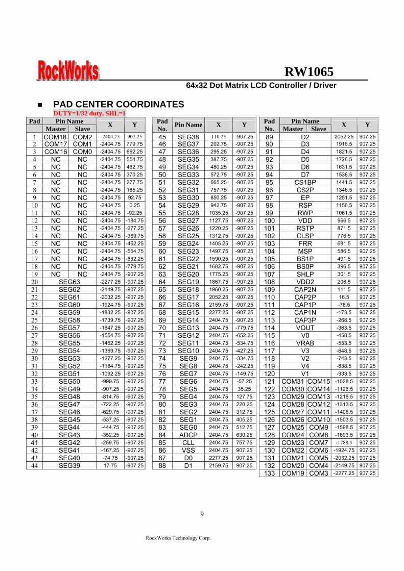
RW1065 64x32 Dot Matrix LCD Controller Driver
RockWorks Technology Corp
9
PAD CENTER COORDINATES DUTY=132 duty SHL=1
Pad Pin Name Pin Name Master Slave X Y
Pad No Pin Name X Y Pad
No Master Slave X Y
1 COM18 COM2 -240475 90725 45 SEG38 11025 -90725 89 D2 205225 907252 COM17 COM1 -240475 77975 46 SEG37 20275 -90725 90 D3 19165 907253 COM16 COM0 -240475 66225 47 SEG36 29525 -90725 91 D4 18215 907254 NC NC -240475 55475 48 SEG35 38775 -90725 92 D5 17265 907255 NC NC -240475 46275 49 SEG34 48025 -90725 93 D6 16315 907256 NC NC -240475 37025 50 SEG33 57275 -90725 94 D7 15365 907257 NC NC -240475 27775 51 SEG32 66525 -90725 95 CS1BP 14415 907258 NC NC -240475 18525 52 SEG31 75775 -90725 96 CS2P 13465 907259 NC NC -240475 9275 53 SEG30 85025 -90725 97 EP 12515 9072510 NC NC -240475 025 54 SEG29 94275 -90725 98 RSP 11565 9072511 NC NC -240475 -9225 55 SEG28 103525 -90725 99 RWP 10615 9072512 NC NC -240475 -18475 56 SEG27 112775 -90725 100 VDD 9665 9072513 NC NC -240475 -27725 57 SEG26 122025 -90725 101 RSTP 8715 9072514 NC NC -240475 -36975 58 SEG25 131275 -90725 102 CLSP 7765 9072515 NC NC -240475 -46225 59 SEG24 140525 -90725 103 FRR 6815 9072516 NC NC -240475 -55475 60 SEG23 149775 -90725 104 MSP 5865 9072517 NC NC -240475 -66225 61 SEG22 159025 -90725 105 BS1P 4915 9072518 NC NC -240475 -77975 62 SEG21 168275 -90725 106 BS0P 3965 9072519 NC NC -240475 -90725 63 SEG20 177525 -90725 107 SHLP 3015 9072520 SEG63 -227725 -90725 64 SEG19 186775 -90725 108 VDD2 2065 9072521 SEG62 -214975 -90725 65 SEG18 196025 -90725 109 CAP2N 1115 9072522 SEG61 -203225 -90725 66 SEG17 205225 -90725 110 CAP2P 165 9072523 SEG60 -192475 -90725 67 SEG16 215975 -90725 111 CAP1P -785 9072524 SEG59 -183225 -90725 68 SEG15 227725 -90725 112 CAP1N -1735 9072525 SEG58 -173975 -90725 69 SEG14 240475 -90725 113 CAP3P -2685 9072526 SEG57 -164725 -90725 70 SEG13 240475 -77975 114 VOUT -3635 9072527 SEG56 -155475 -90725 71 SEG12 240475 -65225 115 V0 -4585 9072528 SEG55 -146225 -90725 72 SEG11 240475 -53475 116 VRAB -5535 9072529 SEG54 -136975 -90725 73 SEG10 240475 -42725 117 V3 -6485 9072530 SEG53 -127725 -90725 74 SEG9 240475 -33475 118 V2 -7435 9072531 SEG52 -118475 -90725 75 SEG8 240475 -24225 119 V4 -8385 9072532 SEG51 -109225 -90725 76 SEG7 240475 -14975 120 V1 -9335 9072533 SEG50 -99975 -90725 77 SEG6 240475 -5725 121 COM31 COM15 -10285 9072534 SEG49 -90725 -90725 78 SEG5 240475 3525 122 COM30 COM14 -11235 9072535 SEG48 -81475 -90725 79 SEG4 240475 12775 123 COM29 COM13 -12185 9072536 SEG47 -72225 -90725 80 SEG3 240475 22025 124 COM28 COM12 -13135 9072537 SEG46 -62975 -90725 81 SEG2 240475 31275 125 COM27 COM11 -14085 9072538 SEG45 -53725 -90725 82 SEG1 240475 40525 126 COM26 COM10 -15035 9072539 SEG44 -44475 -90725 83 SEG0 240475 51275 127 COM25 COM9 -15985 9072540 SEG43 -35225 -90725 84 ADCP 240475 63025 128 COM24 COM8 -16935 9072541 SEG42 -25975 -90725 85 CLL 240475 75775 129 COM23 COM7 -17885 9072542 SEG41 -16725 -90725 86 VSS 240475 90725 130 COM22 COM6 -192475 9072543 SEG40 -7475 -90725 87 D0 227725 90725 131 COM21 COM5 -203225 9072544 SEG39 1775 -90725 88 D1 215975 90725 132 COM20 COM4 -214975 90725 133 COM19 COM3 -227725 90725
RW1065 64x32 Dot Matrix LCD Controller Driver
RockWorks Technology Corp
10
Pin Description
(1)Power Pins
Name IO Description
VDD - Connected to the +5V 0r +3V dc power Common to the Vcc MPU power pin
VDD2 This is the retevence power supply for the Step-up voltage circuit
VSS - 0V dc pin connected to the system ground
CAP1P~3P CAP1N~2N - Capacitor connector pin for voltage booster
V0~V4 - Multi-level power supplies for LCD driving The voltage determined for each liquid crystal cell is divided by resistance or it is converted in impedance by the op amp and supplied These voltages must satisfy the following V0 ≧ V1 ≧ V2 ≧ V3 ≧V4 ≧ VSS
(2)System Bus Connection Pins Name IO Description
D7 to D0 IO The 8-bit bidirectional data buses to be connected to the 8- or 16- bit standard MCU Data busses
RS I Usually connected to the low-order bit of the MPU address bus and used to identify the data or a command RS=0 D0 to D7 are display control data RS=1 D0 to D7 are display data
CLS I CLS=1 internal oscillator enable CLS=0 external clock operation mode
ADCP I
The pin selects the relationship between display data RAM column addresses and segment drivers ADCP=1 SEG0larrcolumn address 3FHhellipinverted ADCP=0 SEG0larrcolumn address 00Hhellipnormal
SHLP I
The pin selects the com output scan direction SHL=1 Reverse directioncom63rarrcom0 SHL=0 Normal com0rarrcom63 Both master and slave should set identical SHL value
BS1PBS0P I
Select LCD Bias 15 16 18 19 bias BS1P=0 BS0P=0 15 bias BS1P=0 BS0P=1 16 bias BS1P=1 BS0P=0 18 bias BS1P=1 BS0P=1 19 bias
RST ―
I Input low active System reset
CS1BP CS2P I Input When CS1BP = 0 and CS2P = 1 the chip select become active
E I For 68-series MPU Input Active high
Used as an enable clock input of the 68-series MPU
RW I For 68-series MPU Input
Used as an input pin of read control signals (if RW is high) or write control signals signals (if low)
RW1065 64x32 Dot Matrix LCD Controller Driver
RockWorks Technology Corp
11
(3)LCD Driver Circuit Signals
Name IO Description
CLL IO
Inputoutput IO selection
MS = ldquoHrdquo amp CLS = ldquoHrdquo Output MS = ldquoLrdquo amp CLS = ldquoHrdquo Input MS = ldquoXrdquo amp CLS = ldquoLrdquo Input
This is a display data latch signal to count up the line counter and common counterat each signal falling and rising edges
SEGn O Output A single level of V0 V2 V3 and VSS is selected by the combination of display RAM contents and FR signal
COMn O Output The output pin for LCD common (row) driving A single level of V0 V1 V4 and VSS is selected by the combination of common counter output and FR signal The slave LSI has the reverse common output scan sequence than the master LSI
FRR IO
Inputoutput This is the liquid crystal alternating current signal IO terminal lO selection
MS = ldquoHrdquoOutput MS = ldquoLrdquoInput
VRAB I Provides the voltage between V0 and VSS through a resistive voltage divider
MS I
Input The master or slave LSI operation select pin for the RW1065
MS OperatingMode FR CL V0~V4 Power
SupplyInternal
OSC COMMON
Output SEG
output
High Master Output See CLS On On See
CLS COM0-31 SEG0-63
Low Slave Input Input Off Off Off COM32-63
SEG64-127
RW1065 64x32 Dot Matrix LCD Controller Driver
RockWorks Technology Corp
12
DESCRIPTION OF FUNCTIONS
The Parallel Interface (6800 series MPU)
Shared 6800 Series
RS RW Function
1 1 Reads the display data
1 0 Writes the display data
0 1 Status read
0 0 Write control data (command)
The Chip Select The RW1065 Series chips have two chip select terminals CS1
―BP and CS2P
When the chip select is inactive D0 to D7 enter a high impedance state and the RS E and RW inputs are inactive
The Accessing the Display Data RAM and the Internal Registers Data transfer at a higher speed is ensured since the MPU is required to satisfy the cycle time (tCYC) requirement alone in accessing the RW1065 Series Wait time may not be considered And in the RW1065 Series chips each time data is sent from the MPU a type of pipeline process between LSIs is performed through the bus holder attached to the internal data bus Internal data bus For example when the MPU writes data to the display data RAM once the data is stored in the bus holder then it is written to the display data RAM before the next data write cycle Moreover when the MPU reads the display data RAM
the first data read cycle (dummy) stores the read data in the bus holder and then the data is read from the bus holder to the system bus at the next data read cycle There is a certain restriction in the read sequence of the display data RAM Please be advised that data of the specified address is not generated by the read instruction issued immediately after the address setup This data is generated in data read of the second time Thus a dummy read is required whenever the address setup or write cycle operation is conducted This relationship is shown in Figure 2
RW1065 64x32 Dot Matrix LCD Controller Driver
RockWorks Technology Corp
13
E
Fig 2b read timing
E
RW
Fig 2a write timing (RW=rdquoLrdquo)
RS
RS
RW1065 64x32 Dot Matrix LCD Controller Driver
RockWorks Technology Corp
14
Display Data RAM The display data RAM is a RAM that stores the dot data for the display It has a 64 (8 page x 8 bit) x 64 bit structure It is possible to access the desired bit by specifying the page address and the column addressBecause as is shown in Figure 3 the D7 to D0 display data from the MPU corresponds to the liquid crystal display common direction there are few constraints at the time of display data transfer when multiple RW1065 series chips are used
thus and display structures can be created easily and with a high degree of freedom Moreover reading from and writing to the display RAM from the MPU side is performed through the IO buffer which is an independent operation from signal reading for the liquid crystal driver Consequently even if the display data RAM is accessed asynchronously during liquid crystal display it will not cause adverse effects on the display (such as flickering)
0
1
0
0
1
1
0
0
1
0
1
0
0
1
0
1
0
0
1
0
0
0
0
0
0
D0
D1
D2
D3
D4
-
Display data RAM Liquid crystal display
COM0
COM1
COM2
COM3
COM4
-
Figure3
The Page Address Circuit As shown in Figure 4 page address of the display data RAM is specified through the Page Address Set Command The page address must be specified again when changing pages to perform access
The Column Address As is shown in Table 4 the display data RAM column address is specified by the Column Address Set command The specified column address is incremented (+1) with each display data readwrite command This allows the MPU display data to be accessed continuously Moreover the increment of column addresses stops with 3FH Because the column address is independent of the page address when moving for example from page 0 column 3FH to page 1
column 00H it is necessary to respecify both the page address and the column address Furthermore as is shown in Table 4 the ADC command (segment driver direction select command) can be used to reverse the relationship between the display data RAM column address and the segment output Because of this the constraints on the IC layout when the LCD module is assembled can be minimized
Table 4 SEG Output
ADC set SEG0 SEG 63
ADC(D0)=0 0 rarr Column Address rarr 63 ADC(D0)=1 63 larr Column Address larr 0
RW1065 64x32 Dot Matrix LCD Controller Driver
RockWorks Technology Corp
15
Figure 4
Page Address D3 D2 D1 D0
DataSE
G0
SEG
1
SEG
2
SEG
3
SEG
4
SEG
5
SEG
6
SEG
7
SEG
8
helliphelliphelliphellip
SEG
55
SEG
56
SEG
57
SEG
58
SEG
59
SEG
60
SEG
61
SEG
62
SEG
63 SEG
COM
D0 COM0
D1 COM1
D2 COM2
D3 COM3
D4 COM4
D5 COM5
D6 COM6
0 0 0 0
D7
Page 0
COM7
D0 COM8
D1 COM9
D2 COM10
D3 COM11
D4 COM12
D5 COM13
D6 COM14
0 0 0 1
D7
Page 1
COM15
D0 COM16
D1 COM17
D2 COM18
D3 COM19
D4 COM20
D5 COM21
D6 COM22
0 0 1 0
D7
Page 2
COM23
D0 COM24
D1 COM25
D2 COM26
D3 COM27
D4 COM28
D5 COM29
D6 COM30
0 0 1 1
D7
Page 3
COM31
ADC=0 00
01
02
03
04
05
06
07
08
helliphelliphelliphellip 55
56
57
58
59
60
61
62
63
COLUMN ADC=1 63
62
61
60
59
58
57
56
55
helliphelliphelliphellip 08
07
06
05
04
03
02
01
00
RW1065 64x32 Dot Matrix LCD Controller Driver
RockWorks Technology Corp
16
Common Timing Generator Circuit Display Data Latch Circuit Generates common timing signals and FR frame signals from the CL basic clock The 132 or 164 duty (for RW1065) can be selected by the Duty Select command The 132 and 164 duties are provided by two chips consisting of the master and slave chips in the common multi-chip mode
This latch stores one line of display data for use by the LCD driver interface circuitry The output of this latch is controlled by the Display ONOFF
132 duty
164 duty
SHL=0
SHL=1
SHL=0
SHL=1
RW1065 64x32 Dot Matrix LCD Controller Driver
RockWorks Technology Corp
17
Display Timing Generator Circuit
The display timing generator circuit generates the timing signal to the line address circuit and the display data latch circuit using the display clock The display data is latched into the display data latch circuit synchronized with the display clock and is output to the data driver output terminal Reading to the display data liquid crystal driver circuits is completely independent of accesses to the display data RAM by the MPU Consequently even if the display data
RAM is accessed asynchronously during liquid crystal display there is absolutely no adverse effect (such asflickering) on the display Moreover the display timing generator circuit generates the common timing and the liquid crystal alternating current signal (FR) from the display clock It generates a drive wave form using a 2 frame alternating current drive method as is shown in Figure 5 for the liquid crystal drive circuit
Two-frame alternating current drive waveform
Figure 5
When multiple RW1065 Series chips are used the slave chip must be supplied the display timing signals(FR CL) from the master chip
Table 5 shows the status of the FR and CL signals
Table 5 Operating Mode FR CL
Master (MS = ldquoHrdquo) The internal oscillator circuit is enabled (CLS = ldquoHrdquo) The internal oscillator circuit is disabled (CLS = ldquoLrdquo)
Output Output
Output Input
Slave (MS = ldquoLrdquo) The internal oscillator circuit is enabled (CLS = ldquoHrdquo) The internal oscillator circuit is disabled (CLS = ldquoLrdquo)
Input Input
Input Input
RW1065 64x32 Dot Matrix LCD Controller Driver
RockWorks Technology Corp
18
The Liquid Crystal Driver Circuits
These are a 64-channel (RW1065) that generate four voltage levels for driving the liquid crystal The combination of the display data the COM scan signal and the FR signal
produces the liquid crystal drive voltage output Figure 6 shows examples of the SEG and COM output waveform
Figure 6
RW1065 64x32 Dot Matrix LCD Controller Driver
RockWorks Technology Corp
19
The Power Supply Circuit
The power supply circuits are low-power consumption power supply circuits that generate the voltage levels required for the liquid crystal drivers They comprise Booster circuits and voltage follower circuits They are only enabled in master operation The power supply circuits can turn on automatically after power on
Consequently it is possible to make an external power supply and the internal power supply function somewhat in parallel
The Liquid Crystal Voltage Generator Circuit The V0 voltage is produced by a resistive voltage divider outside the IC through VRAB pin and can be produced at the V1 V2 V3 and V4 voltage levels required for liquid crystal driving Moreover when the voltage follower changes the impedance it provides V1 V2 V3 and V4 to the liquid crystal drive circuit 15 bias or 16 bias or 18 bias or 19 bias for RW1065 can be selected by BS0 and BS1 pins V0-Vss maximum voltage is 15V Vout-Vss maximum voltage is 17V If VDD lt 35V it can use the Booster circuit 2x3x4xThe booster voltage can follow the spec condition (Vout-Vss ≦ 17V max voltage) if VDD gt35V only use the 2X3X booster circuit that can ensure the V0-Vss voltage ≦ 15V If use the VDD voltage 5V and 4X booster itrsquos over the spec operation condition To turn on built-in power (boosterfollower) must waiting 200mS to display on for boosterfollower stable Therefore power off must follower ldquopower off sequencerdquo too
Power on Display off
Power off
Power off sequence
Wait time gt200mS
Display on
Power on sequence
RW1065 64x32 Dot Matrix LCD Controller Driver
RockWorks Technology Corp
20
The Reset Circuit
When the RTP input comes to the ldquoLrdquo level these LSIs return to the default state Their default states are as follows 1 Display OFF 2 Display all point on is select to normal 3 Display normalreverse is select to normal 4 164 duty is selected 5 Read modify write OFF 6 Column address set to Address 0 7 Page address set to Page 0 8 Start line set to first line 9 Frame frequency set to default 10 Power save mode released 11 Ext set to ldquo0rdquo When the power is turned on the IC internal state becomes unstable and it is necessary to initialize it using the RSTP terminal After the initialization each input terminal should be controlled normally While RSTP is ldquoLrdquo the oscillator works but the display timing generator stops and the CL FR terminals are fixed to ldquoHrdquo The terminals D0 to D7 are not affected
RW1065 64x32 Dot Matrix LCD Controller Driver
RockWorks Technology Corp
21
TABLE OF RW1065 INSTRUCTIONS
Instruction code Instruction RS RW DB7 DB6 DB5 DB4 DB3 DB2 DB1 DB0 Description
EXT=0 or 1
MODE SET 0 0 0 0 0 0 1 1 0 EXT Set EXT mode
Instruction code Instruction RS RW DB7 DB6 DB5 DB4 DB3 DB2 DB1 DB0 Description
EXT=0 Display ONOFF 0 0 0 0 1 1 1 1 1 D D=0Display OFF
D=1Display ONSet page address 0 0 1 0 1 1 1 P2 P1 P0 Set page address
Set column address 0 0 0 1 Y5 Y4 Y3 Y2 Y1 Y0 Set column
address MSB
Read Status 0 1 BUSY 0 ON OFF RESET 0 0 0 0 Read register
status Write display
data 1 0 Write data Write data into DDRAM
Read display data 1 1 Read data Read data from
DDRAM Set initial
display line register
0 0 1 1 S5 S4 S3 S2 S1 S0 Specify the initial
display line to realize vertical scrolling
Instruction code Instruction RS RW DB7 DB6 DB5 DB4 DB3 DB2 DB1 DB0 Description
EXT=1
NOP 0 0 0 0 0 0 0 0 0 0 no operation
Set modiy-read 0 0 0 0 0 0 1 0 0 0 Set modiy-read
mode
END 0 0 0 0 0 0 1 1 1 0 release modiy-read mode
Set power save mode 0 0 0 0 0 0 0 0 1 PSAVE P=0 normal mode
P=1 sleep mode
0 0 0 0 0 1 0 1 Display
COMMAND (double
command)
0 0 FRSEL
0 0 0 0 REV ALLON DUTY
DUTY=1 64 duty DUTY=0 32 duty ALLON=1display all on ALLON=0display
normal REV=1display reverse REV=0display normal FRSEL=1FR frequency double default FRSEL=0FR frequency default
RW1065 64x32 Dot Matrix LCD Controller Driver
RockWorks Technology Corp
22
Command Description
See the Table of RW1065 instructions The RW1065 series identifies a data bus using a combination of RS E and RW signals As the MPU translates a command in the internal timing only (independent from the external clock) its speed is very high The busy check is usually not required
Display ONOFF
EXT RS RW D7 D6 D5 D4 D3 D2 D1 D0
0 0 0 0 0 1 1 1 1 1 D
This command turns the display on and off D=1 Display ON D=0 Display OFF(default)
Set page Address This command specifies the page address that corresponds to the low address of the display data RAM when it is accessed by the MPU Any bit of the display data RAM can be accessed when its page address and column address are specified The display status is not changed even when the page address is changed
EXT RS RW D7 D6 D5 D4 D3 D2 D1 D0
0 0 0 1 0 1 1 1 A2 A1 A0
This command loads the page address register
A2 A1 A0 Page
0 0 0 0 (default)
0 0 1 1 0 1 0 2 0 1 1 3 1 0 0 4 1 0 1 5 1 1 0 6 1 1 1 7
Page mapping see Figure 4
RW1065 64x32 Dot Matrix LCD Controller Driver
RockWorks Technology Corp
23
Set Column Address This command specifies a column address of the display data RAM When the display data RAM is accessed by the MPU continuously the column address is incremented by I each time it is accessed from the set address Therefore the MPU can access to data continuously The column address stops to be incremented at address 63 and the page address is not changed continuously
EXT RS RW D7 D6 D5 D4 D3 D2 D1 D0
0 0 0 0 1 A5 A4 A3 A2 A1 A0
A5 A4 A3 A2 A1 A0 Column Address0 0 0 0 0 0 0(default) 0 0 0 0 0 1 1
1 1 1 1 1 1 63
Read Status
EXT RS RW D7 D6 D5 D4 D3 D2 D1 D0
0 0 1 BUSY 0 ON OFF RESET 0 0 0 0
The BUSY Flag bit indicates that RW 1065 is operating or no operating
BUSY=1 Operation BUSY=0 Ready
The ONOFF bit indicates the current status of the display It is the inverse of the polarity of the display ONOFF command ONOFF=1 Display OFF ONOFF=0 Display ON The RESET bit indicates whether the driver is executing a hardware or software reset or if it is in normal operating mode RESET=1 Currently executing reset command RESET=0 Normal operation
RW1065 64x32 Dot Matrix LCD Controller Driver
RockWorks Technology Corp
24
Write Display Data
EXT RS RW D7 D6 D5 D4 D3 D2 D1 D0
0 1 0 Write data
Writes 8-bits of data into the display data RAM at a location specified by the contents of the column address and page address registers and then increments the column address register by one
Read Display Data
EXT RS RW D7 D6 D5 D4 D3 D2 D1 D0
0 1 1 Read data
Reads 8-bits of data from the data IO latch updates the contents of the IO latch with display data from the display data RAM location specified by the contents of the column address and page address registers and then increments the column address register After loading a new address into the column address register one dummy read is required before valid data is obtained
Set initial display line register
EXT RS RW D7 D6 D5 D4 D3 D2 D1 D0
0 0 0 1 1 S5 S4 S3 S2 S1 S0
Loads the RAM line address of the initial display line COM 0 into the initial display line register The RAM display data becomes the top line of the LCD screen It is followed by the higher number lines in ascending order corresponding to the duty cycle The screen can be scrolled using this command by incrementing the line address(default value=rdquo00Hrdquo)
RW1065 64x32 Dot Matrix LCD Controller Driver
RockWorks Technology Corp
25
Read-Modify-Write
EXT RS RW D7 D6 D5 D4 D3 D2 D1 D0
1 0 0 0 0 0 0 1 0 0 0
This command defeats column address register auto-increment after data reads The current contents of the column Address register are saved The mode remains active until an End command is received When the End command is entered the column address is returned to the one used during input of Read-Modify-Write Command This function can reduce the load of MPU when data change is repeated as a specific display area Any command other than Data Read or Write can be used in the Read-Modify-Write mode However the Column Address Set command cannot be used
End
EXT RS RW D7 D6 D5 D4 D3 D2 D1 D0
1 0 0 0 0 0 0 1 1 1 0
This command cancels read-modify-write mode and restores the contents of the column address register to their value prior to the receipt of the Read-Modify-Write command
N N+1 N+2 N+3 N+m N
Read -modify-write mode set End
Returm
Column address
Set page address
Set column address
Read-modify-write
Dummy read
Read data
Write data
End
CompletedNo
Yes
RW1065 64x32 Dot Matrix LCD Controller Driver
RockWorks Technology Corp
26
Set power save mode
EXT RS RW D7 D6 D5 D4 D3 D2 D1 D0
1 0 0 0 0 0 0 0 0 1 PSAVE
When power save mode is entered thus greatly reducing power consumption In the power save mode the display data is saved as is the operating mode that was in effect before the power saver mode was initiated and the MPU is still able to access the display data RAM PSAVE=1 Sleep mode PSAVE=0 Normal mode Sleep mode This stops all operations in the LCD display system and as long as there are no accesses from the MPU the consumption current is reduced to a value near the static current The internal modes during sleep mode are as follows 1 The oscillator circuit and the LCD power supply circuit are halted 2 All liquid crystal drive circuits are halted and the segment and common drive outputs output a Vss level
Display command double command
EXT RS RW D7 D6 D5 D4 D3 D2 D1 D0
1 0 0 0 0 0 0 0 1 0 1
1 0 0 FRSEL 0 0 0 0 REV ALLON DUTY
Display NormalReverse set REV=1 Reverse REV=0 Normal(default) Display All Point ONOFF ALLON=1 All display points ON ALLON=0 Normal(default) Select Duty Duty=1 164 duty cycle(default) Duty=0 132 duty cycle FRAME FREQUENCY Select FRSEL=1 Double FRSEL=0 (default)
RW1065 64x32 Dot Matrix LCD Controller Driver
RockWorks Technology Corp
27
Hardware Pin Set
Select ADC by ADC Pin The pin selects the relationship between display data RAM column addresses and segment drivers ADC=1 SEG0larrcolumn address 3FHhellipinverted ADC=0 SEG0larrcolumn address 00Hhellipnormal(default) This command is provided to reduce restrictions on the placement of driver ICs and routing of traces during printed circuit Board design See Figure 4 for a table of segments and column addresses for the two values of D
Select SHL by SHL Pin The pin selects the com output scan direction SHL=1 Reverse directioncom63rarrcom0 SHL=0 Normal com0rarrcom63 Both master and slave should set identical SHL value
Select LCD Bias by BS0 BS1 Pin
BS1 BS0 Bias 0 0 15 bias 0 1 16 bias 1 0 18 bias 1 1 19 bias
RW1065 64x32 Dot Matrix LCD Controller Driver
RockWorks Technology Corp
28
When an External Resistance is Used The liquid crystal power supply voltage V0 is set by adding resistors Rarsquo and Rbrsquo between VDD and VR and between VR and V0 respectively
RW1065
RW1065 64x32 Dot Matrix LCD Controller Driver
RockWorks Technology Corp
29
The set voltage circuits
Using the step-up voltage circuits equipped within the RW1065 chips it is possible to produce a 2X 3X 4X step-up voltage levels 2X step-up
To produce voltage level in the positive direction at the Vout terminal that is 2 times the voltage difference between VSS and VDD2 Please configure set voltage circuits like this Place a 1uF~22uF capacitor between CAP1N and CAP1P Place a 1uF~22uF capacitor between VSS and VOUT Short CAP2P CAP3P and VOUT Leave CAP2N open 3X step-up
To produce voltage level in the positive direction at the Vout terminal that is 3 times the voltage difference between VSS and VDD2 Please configure set voltage circuits like this Place a 1uF~22uF capacitor between CAP1N and CAP1P Place a 1uF~22uF capacitor between VSS and VOUT Place a 1uF~22uF capacitor and 100 ohms resistor between CAP2N and CAP2P Short CAP3P and Vout 4X step-up
To produce voltage level in the positive direction at the Vout terminal that is 4 times the voltage difference between VSS and VDD2 Please configure set voltage circuits like this Place a 1uF~22uF capacitor between CAP1N and CAP1P Place a 1uF~22uF capacitor between VSS and VOUT Place a 1uF~22uF capacitor and 100 ohms resistor between CAP2N and CAP2P Place a 1uF~22uF capacitor and 100 ohms resistor between CAP1N and CAP3P
RW1065 64x32 Dot Matrix LCD Controller Driver
RockWorks Technology Corp
30
ABSOLUTE MAXIMUM RATINGS Characteristics Symbol Value Unit
Power supply voltage VDD -03 to +70 V
LCD driver voltage Vout 0 to +17 V
Input voltage VIN -03 to VDD+03 V
Operating temperature TA -40 to +85
Storage temperature TSTO -55 to +125
DC CHARACTERISTICS
Rating Item Symbol Condition Min Typ Max Unit ApplicablePin
Operating Voltage VDD - 27 30 55 V VDD1
Step up output voltage Vout (Relative to VDD) 0 - 17 V Vout
Voltage follower circuit operating Voltage V0 (Relative to VDD) 0 - 15 V V0
V0 accuracy V0 - 0 - 15 V0
High-level Input Voltage Low-level Input Voltage
VIHC VILC - 07 VDD
Vss - VDD 09 V 2
High-level Output Voltage Low-level Output Voltage
VOHC VOLC
IOH = ndash05 mA IOL = 05 mA
08VDD Vss - VDD
02 VDD V 3
Input leakage current ILI VIN = VDD or VSS -1 - 2 uA 4
Output leakage current ILO - -1 1 uA 5
Liquid Crystal Driver ON Resistance RON
Ta= 25degC(Relative To VDD)
V0 =15 V - 16 20 KΩ SEGn COMn 6
Internal Oscillator fOSC 2286 254 2794 Oscillator
Frequency External Input RECOMMAND fCL
Ta = 25degC 132Duty 2286 254 2794
kHz CL
Internal Oscillator fOSC 45 5 55 Oscillator
Frequency External Input RECOMMAND fCL
Ta = 25degC 164Duty 45 5 55
kHz CL
bullDynamic Consumption Current During Display with the Internal Power Supply OFF Current consumed by total ICs when an external power supply is used
Unless otherwise specified Vss=0V VDD=30V
RW1065 64x32 Dot Matrix LCD Controller Driver
RockWorks Technology Corp
31
Display Pattern OFF
Ta = 25degC Vout=17V Rating Item Symbol Condition Min Typ Max Unit Notes
VDD=30 V V0-Vss=8V - 10 15 RW1065 IDD VDD=50 V V0-Vss=8V - 35 45
microA 7
Display Pattern Checker
Ta = 25degC Vout=17V Rating Item Symbol Condition Min Typ Max Unit Notes
VDD=30 V V0-Vss=8V - 15 20 RW1065 IDD VDD=50 V V0-Vss=8V - 40 50
microA 7
Display Pattern OFF
Ta = 25degC Vout=17V Rating Item Symbol Condition Min Typ Max Unit Notes
VDD=30 V V0-Vss=8V - 15 20 RW1065 IDD VDD=50 V V0-Vss=8V - 40 50
microA 7
Display pattern Checker
Ta = 25degC Vout=17V Rating Item Symbol Condition Min Typ Max Unit Notes
VDD=30 V V0-Vss=8V - 65 80 RW1065 IDD VDD=50 V V0-Vss=8V - 130 150
microA 7
bull Consumption Current at Time of Power Saver Mode VSS = 0 V VDD = 30 V plusmn 10
Rating Item Symbol Condition Min Typ Max Unit Notes
Sleep mode IDD - - 5 10 microA -
References for items market with 1 While a broad range of operating voltages is guaranteed performance cannot be guaranteed if there are sudden fluctuations to the
voltage while the MPU is being accessed 2 The RS D0 to D5 D6 D7 E RW CS1BP CS2P CLS CL FR MS and RST
― terminals
3 The D0 to D7 FR and CL terminals 4 The RS E RW CS1BP CS2P CLS MS and RST
― terminals
5 Applies when the D0 to D5 D6 D7 CL and FR terminals are in a high impedance state 6 These are the resistance values for when a 01 V voltage is applied between the output terminals SEGn or COMn and
the various power supply terminals (V1 V2 V3 and V4) These are specified for the operating voltage (3) range RON = 01 V ∆I (Where ∆I is the current that flows when 01 V is applied while the power supply is ON)
7 It indicates the current consumed on ICs alone when the internal oscillator circuit and display are turned on Does not include the current due to the LCD panel capacity and wiring capacity Applicable only when there is no access from the MPU
RW1065 64x32 Dot Matrix LCD Controller Driver
RockWorks Technology Corp
32
TIMING CHARACTERISTICS
68 Interface
(Ta=-40 to 85 degC) VDD=27 to 45V
Rating VDD=45 to 55V
Rating Item Signal Symbol ConditionMin Max Min Max
Units
Address hold time RS tAH6 0 mdash 0 mdash Address setup time RS tAW6
mdash 0 mdash 0 mdash
ns
System cycle time RS tCYC6 mdash 900 mdash 800 mdash ns Data setup time D0 to D7 tDS6 100 mdash 100 mdash Data hold time D0 to D7 tDH6
mdash 0 mdash 0 mdash
ns
Access time D0 to D7 tACC6 mdash 350 mdash 250
Output disable time D0 to D7 tOH6 CL = 100 pF
mdash 300 mdash 200 ns
Read tEWHR 360 mdash 300 mdash Enable H pulse time
WriteE
tEWHW mdash
360 mdash 300 mdash ns
Read tEWLR 450 mdash 400 mdash Enable L pulse time
WriteE
tEWLW mdash
450 mdash 400 mdash ns
1 All timing is specified using 20 and 80 of VDD as the reference 2 tEWLW and tEWLR are specified as the overlap between CS1BP being ldquoLrdquo (CS2P = ldquoHrdquo) and E
RW1065 64x32 Dot Matrix LCD Controller Driver
RockWorks Technology Corp
33
Reset Timing
Rating Item Signal Symbol Condition
Min Typ Max Units
Reset time mdash tR mdash mdash - 2 micros
Reset ldquoLrdquo pulse width RST tRW mdash 2 - mdash micros
1 When double chip was be used then the duty set command must be set between the tR
RW1065 64x32 Dot Matrix LCD Controller Driver
RockWorks Technology Corp
34
IO PAD CONFIGURATION
RW1065 64x32 Dot Matrix LCD Controller Driver
RockWorks Technology Corp
35
THE MPU INTERFACE (REFERENCE EXAMPLES) The RW1065 Series can be connected to 6800 Series MPUs The display area can be enlarged by using multiple RW1065 Series chips When this is done the chip select signal can be used to select the individual ICs to access
6800 Series MPUs
RW
106
5
RW1065 64x32 Dot Matrix LCD Controller Driver
RockWorks Technology Corp
36
When using external multi-level power supply for LCD driving (REFERENCE EXAMPLE)
Using a resistor divider can provide RW1065 external multi-level power supply for LCD driving
The circuit below shows a resistor divider network which can bias V0 V1 V2 V3 and V4 externally
RW1065 64x32 Dot Matrix LCD Controller Driver
RockWorks Technology Corp
37
bullWhen V0 V1 V2 V3 and V4 are biased by external power supply analog section of RW1065 should be turn off by software during LCD initialization The example in below shows the sequence to turn off analog section when external bias is used Begin of LCD initialization 1 Reset RW1065 2 SET EXT=1 (mode instruction)
RS RW DB7 DB6 DB5 DB4 DB3 DB2 DB1 DB00 0 0 0 0 0 1 1 0 1
3 SET Display Command (double command)
RS RW DB7 DB6 DB5 DB4 DB3 DB2 DB1 DB00 0 0 0 0 0 0 1 0 1 0 0 0 0 1 1 0 0 0 1
4 SET EXT=1 (mode instruction)
RS RW DB7 DB6 DB5 DB4 DB3 DB2 DB1 DB00 0 0 0 0 0 1 1 0 0
End of LCD initialization
bullBecause pins can not set LCD bias when external power supplies are used for LCD driving the bias can be set by an appropriate configuration for a resistor voltage divider networks The example is shown below
VSS
R
R
NR
R
R
RV1
RV2
RV3
RV4
V0
Bias Network Circuit Concept 15 Bias N=1 total = 5R 16 Bias N=2 total =6R 18 Bias N=4 total =8R 19 Bias N=5 total = 9R
RW1065 64x32 Dot Matrix LCD Controller Driver
RockWorks Technology Corp
38
Single chip solution for RW1065 application (REFERENCE EXAMPLE)
For a 64x32 application the duty cycle of LCD panel is 164 and the display duty of RW1065 should be set to 164 The display duty cycle can be selected by the DUTY bit in display command The diagram for 64x32 application is shown below
64 SEGx32COM LCD Panel
164 duty cycle
RW1065 DUTY=1
COM1~33
SEG1~65
RW1065 64x32 Dot Matrix LCD Controller Driver
RockWorks Technology Corp
39
Using an adjustable resistor on the main board to adjust the contrast of liquid crystal display (REFERENCE EXAMPLE)
The schematic shows an adjustable resistor on main board that can adjust voltage level of V0
RW1065 64x32 Dot Matrix LCD Controller Driver
RockWorks Technology Corp
40
Package information (Please pay close attention to the information in this section Do not hesitate to consult with our sale representative if you have any question or concern)
In order to make better bonding yield for RW1065 please follow the tips and recommendations in this section In this section few tips about COB footprint style PCB layout and wire bonding will be discussed
The drawing in below shows the PCB footprint style which we recommend for RW1065 Pads array in
curve shape is easier for Al wire bonding Besides that a real size COB footprint for RW1065 is also shown in below RW1065 COB footprint is also available in powerpcb or protel format for design reference purpose
The ratio is 11
RW1065 64x32 Dot Matrix LCD Controller Driver
RockWorks Technology Corp
41
During COB footprint design there have some tips about footprint that the PCB designer should know The angle between bonding wire and vertical line should less than 45 Otherwise the wire shorts would become very easy to happen at fours corners of the chip
The angle between bonding wire and vertical line could be reduced by expanding the distance between pads array and the chip In addition reducing length in horizon direction of pads array could minimize the angle between bonding wire and vertical line The picture in below will help to illustrate this concept From the experiences COB footprint style affects the bonding yield
Bad Wires are too close to each other
The angle between bonding wire and vertical line is greater than 45
The angle between bonding wire and vertical line is less than 45
Wires are not too close to each other
Reducing length in horizon direction of pads array could minimize the angle between bonding wire and vertical line
The angle between bonding wire and vertical line could be reduced by expanding the distance between pads array and the chip
RW1065 64x32 Dot Matrix LCD Controller Driver
RockWorks Technology Corp
42
If the gap between pads of COB footprint is filled with solder mask coating it is difficult to bond Al wire to
the pads The top solder masks layer that overlap COB footprint area should be removed
Please use 1 mils diameter Al wire for RW1065 wire bonding
1 2 3 4 5 6
A
B
C
D
654321
D
C
B
A
Title
Number RevisionSize
C
Date 29-Aug-2007 Sheet of File D公司資料99seMyDesignddb Drawn By
RW1065
COM131
COM142
COM153
COM164
COM175
COM186
COM197
COM208
COM219
COM2210
COM2311
COM2412
COM2513
COM2614
COM2715
COM2816
COM2917
COM3018
COM3119
SEG
6320
SEG
6221
SEG
6122
SEG
6023
SEG
5924
SEG
5825
SEG
5726
SEG
5627
SEG
5528
SEG
5429
SEG
5330
SEG
5231
SEG
5132
SEG
5033
SEG
4934
SEG
4835
SEG
4736
SEG
4637
SEG
4538
SEG
4439
SEG
4340
SEG
4241
SEG
4142
SEG
4043
SEG
3944
SEG
3845
SEG
3746
SEG
3647
SEG
3548
SEG
3449
SEG
3350
SEG
3251
SEG
3152
SEG
3053
SEG
2954
SEG
2855
SEG
2756
SEG
2657
SEG
2558
SEG
2459
SEG
2360
SEG
2261
SEG
2162
SEG
2063
SEG
1964
SEG
1865
SEG
1766
SEG
1667
SEG
1568
SEG
1469
SEG13 70SEG12 71SEG11 72SEG10 73SEG9 74SEG8 75SEG7 76SEG6 77SEG5 78SEG4 79SEG3 80SEG2 81SEG1 82SEG0 83ADCP 84CLL 85
VSS
86D
087
D1
88D
289
D3
90D
491
D5
92D
693
D7
94C
S1B
P95
CS2
P96
ERD
P97
AO
P(R
S)98
RW
RP
99V
DD
100
RST
P10
1C
LSP
102
FRR
103
MSP
104
BS1
P10
5B
S0P
106
SHLP
107
VD
D2
108
CA
P2N
109
CA
P2P
110
CA
P1P
111
CA
P1N
112
CA
P3P
113
VO
UT
114
V0
115
VR
AB
116
V3
117
V2
118
V4
119
V1
120
CO
M0
121
CO
M1
122
CO
M2
123
CO
M3
124
CO
M4
125
CO
M5
126
CO
M6
127
CO
M7
128
CO
M8
129
CO
M9
130
CO
M10
131
CO
M11
132
CO
M12
133
4897x1902 um
IC1
RW1065
C9CAPR4
100R0603
R30R0603
C8
CAP
C7
CAP
R2
100R0603
R1
0R0603C6 22uf
R50R
R6300R
R7RES1
R8NC R9
100R0603
VDD
R10
NC
R11
100R0603
R12
100R0603
R13
NC
R14
100R0603
R15
NC
VDD
D0
D1
D2
D3
D4
D5
D6
D7
DB[07]
VDDC5
01uf0603
VD
D
CS2
P
123456789
1011121314151617181920
J1
CON20
C1201uf0603
R3951K0603
VDD
CAP Value1UF~22UF
2XPut C6C8 Short R1R3Open R2R4C7C93XPut C6C8C9 R4Short R1Open R2R3C74XOpen R1R3
BS0 BS1 Bias0 0
0 1
1 0
11
15 bias
16 bias
18 bias
19 bias
ADC=0 SEG0lt~column address 00Hnormal(default) ADC=1 SEG0lt~column address 3FHinverted
SHL=0 Normal COM0~gtCOM63(default)SHL=1 Reverse direction COM63~gtCOM0
R16100R0603
LCD PANEL 64X32RockWorks
RW1065 64X32
COM0-31 SEG0-63SHL=0 ADC=0
SHL=1COM31-0
ADC=1SEG63-0
if use single chip for 32 command displaythe display command must select 164 dutyDisplay panel must select 164 duty type
VO
UT
C3P
C1N
C1P
C2P
C2N
VDD2
ADC
SHL
BS0
BS1
CLLADC
V1
V2
V3
V4
VR
AB
V0
VO
UT
C3P
C1N
C1P
C2P
C2N
VD
D2
SHL
BS0
BS1
FRR
RST
P
RW
RS
E CS1
B
CS1
V0RSRWED0D1D2D3D4D5D6D7
RSTPAK
C4
22uf
RBRES1
RA1RES1
C2
22uf
C1
22uf
C3
22uf
C0
22uf
R20
100k0603
R21
100k0603
R17
200K0603
V1
V2
V3
V4 VRAB
V0
V0
OPTION
B
R18
300R0603
RA2RES1
VADJ
R19100R
R23 RES1R22 0R
R24
RES1
R25
0R
VDD
CS1BP
CS2P
CS1
CS1
R26
22R0603
R27
22R0603
C1047uf
C11
01uf
VSS_INVDD_IN
D1DIODE
FGND
鐵框地
VSS
VDD
R28 10RR29 10RR30 10RR31 10RR32 10RR33 10RR34 10RR35 10RR36 10RR37 10RR38 10R
VADJ
1 2 3 4 5 6
A
B
C
D
654321
D
C
B
A
Title
Number RevisionSize
C
Date 29-Aug-2007 Sheet of File D公司資料99seMyDesignddb Drawn By
RW1065
COM131
COM142
COM153
COM164
COM175
COM186
COM197
COM208
COM219
COM2210
COM2311
COM2412
COM2513
COM2614
COM2715
COM2816
COM2917
COM3018
COM3119
SEG
6320
SEG
6221
SEG
6122
SEG
6023
SEG
5924
SEG
5825
SEG
5726
SEG
5627
SEG
5528
SEG
5429
SEG
5330
SEG
5231
SEG
5132
SEG
5033
SEG
4934
SEG
4835
SEG
4736
SEG
4637
SEG
4538
SEG
4439
SEG
4340
SEG
4241
SEG
4142
SEG
4043
SEG
3944
SEG
3845
SEG
3746
SEG
3647
SEG
3548
SEG
3449
SEG
3350
SEG
3251
SEG
3152
SEG
3053
SEG
2954
SEG
2855
SEG
2756
SEG
2657
SEG
2558
SEG
2459
SEG
2360
SEG
2261
SEG
2162
SEG
2063
SEG
1964
SEG
1865
SEG
1766
SEG
1667
SEG
1568
SEG
1469
SEG13 70SEG12 71SEG11 72SEG10 73SEG9 74SEG8 75SEG7 76SEG6 77SEG5 78SEG4 79SEG3 80SEG2 81SEG1 82SEG0 83ADCP 84CLL 85
VSS
86D
087
D1
88D
289
D3
90D
491
D5
92D
693
D7
94C
S1B
P95
CS2
P96
ERD
P97
AO
P(R
S)98
RW
RP
99V
DD
100
RST
P10
1C
LSP
102
FRR
103
MSP
104
BS1
P10
5B
S0P
106
SHLP
107
VD
D2
108
CA
P2N
109
CA
P2P
110
CA
P1P
111
CA
P1N
112
CA
P3P
113
VO
UT
114
V0
115
VR
AB
116
V3
117
V2
118
V4
119
V1
120
CO
M0
121
CO
M1
122
CO
M2
123
CO
M3
124
CO
M4
125
CO
M5
126
CO
M6
127
CO
M7
128
CO
M8
129
CO
M9
130
CO
M10
131
CO
M11
132
CO
M12
133
4897x1902 um
IC1
RW1065 Master
RW1065
COM131
COM142
COM153
COM164
COM175
COM186
COM197
COM208
COM219
COM2210
COM2311
COM2412
COM2513
COM2614
COM2715
COM2816
COM2917
COM3018
COM3119
SEG
6320
SEG
6221
SEG
6122
SEG
6023
SEG
5924
SEG
5825
SEG
5726
SEG
5627
SEG
5528
SEG
5429
SEG
5330
SEG
5231
SEG
5132
SEG
5033
SEG
4934
SEG
4835
SEG
4736
SEG
4637
SEG
4538
SEG
4439
SEG
4340
SEG
4241
SEG
4142
SEG
4043
SEG
3944
SEG
3845
SEG
3746
SEG
3647
SEG
3548
SEG
3449
SEG
3350
SEG
3251
SEG
3152
SEG
3053
SEG
2954
SEG
2855
SEG
2756
SEG
2657
SEG
2558
SEG
2459
SEG
2360
SEG
2261
SEG
2162
SEG
2063
SEG
1964
SEG
1865
SEG
1766
SEG
1667
SEG
1568
SEG
1469
SEG13 70SEG12 71SEG11 72SEG10 73SEG9 74SEG8 75SEG7 76SEG6 77SEG5 78SEG4 79SEG3 80SEG2 81SEG1 82SEG0 83ADCP 84CLL 85
VSS
86D
087
D1
88D
289
D3
90D
491
D5
92D
693
D7
94C
S1B
P95
CS2
P96
ERD
P97
AO
P(R
S)98
RW
RP
99V
DD
100
RST
P10
1C
LSP
102
FRR
103
MSP
104
BS1
P10
5B
S0P
106
SHLP
107
VD
D2
108
CA
P2N
109
CA
P2P
110
CA
P1P
111
CA
P1N
112
CA
P3P
113
VO
UT
114
V0
115
VR
AB
116
V3
117
V2
118
V4
119
V1
120
CO
M0
121
CO
M1
122
CO
M2
123
CO
M3
124
CO
M4
125
CO
M5
126
CO
M6
127
CO
M7
128
CO
M8
129
CO
M9
130
CO
M10
131
CO
M11
132
CO
M12
133
4897x1902 um
IC2
RW1065 Slave
C4
22uf
RBRES1
RA1RES1
C2
22uf
C1
22uf
C3
22uf
C0
22ufC9CAPR4
100R0603
R30R0603
C8
CAP
C7
CAP
R2
100R0603
R1
0R0603C6 22uf
R50R0603
R6300R0603
R7RES1
R8NC R9
100R0603
VDD
R10
NC
R11
100R0603
R12
NC
R13
100R0603
R14
100R0603
R15
NC
R16
100R0603
R17
NC
VDD
D0
D1
D2
D3
D4
D5
D6
D7
D0
D1
D2
D3
D4
D5
D6
D7
DB[07] DB[07]
VDDC10
01uf0603
VD
D
IC1_
CS2
P
VDD
IC2_
CS2
P
VD
D
C11
01uf0603
VSS
VSS
LCD PANEL 128X64
Master COM0-31 Slave COM32-63
Master SEG0-63 Slave SEG64-127
123456789
1011121314151617181920
J1
CON20
Master Slave
CAP Value1UF~22UF
2XPut C6C8 Short R1R3Open R2R4C7C93XPut C6C8C9 R4Short R1Open R2R3C74XOpen R1R3
RockWorksRW1065 128x64
BS0 BS1 Bias0 0
0 1
1 0
11
15 bias
16 bias
18 bias
19 bias
ADC=0 SEG0lt~column address 00Hnormal(default) ADC=1 SEG0lt~column address 3FHinverted
SHL=0 Normal COM0~gtCOM63(default)SHL=1 Reverse direction COM63~gtCOM0Both Master and Slave should set identical SHL value
SHL=0 SHL=0
ADC=0 ADC=0
Slave COM31-0
Slave SEG127-64
SHL=1
ADC=1
SHL=1Master COM63-32
ADC=1Master SEG63-0
R18100R0603
R22
100k0603
R23
100k0603
C501uF0603
R4551K0603
VDD
R19
200K0603
ADC1
ADC2
SHL
BS0
BS1
VDD2
V1
V2
V3
V4 VRAB
V0
V0V
OU
T
C3P
C1N
C1P
C2P
C2N
V1
V2
V3
V4
VR
AB
V0
VO
UT
C3P
C1N
C1P
C2P
C2N
VD
D2
SHL
BS0
BS1
FRR
RST
P
RW
RS
E IC1_
CS1
BP
V1
V2
V3
V4
VR
AB
V0
VO
UT
VD
D2
SHL
BS0
BS1
FRR
RST
P
RW
RS
E IC2_
CS1
BP
CLLADC1
CLLADC2
RSTP
CS1CS2
V0RSRWED0D1D2D3D4D5D6D7
AK
OPTION
R20
300R0603
RA2RES1
VADJ
R21
100R
B
R25 RESR24 0R
R26 RES R27 0RVDD
IC1_CS1BP
IC1_CS2P
CS1
CS1
R28 0R R29 RES
R30 RES R31 0R
IC2_CS1BP
IC2_CS2P
CS2
CS2
R32
22R0603
R33
22R0603
C1001uf
C11
47uf
D1DIODE
FGND
鐵框地
VSS
VDD
R34 10RR35 10RR36 10RR37 10RR38 10RR39 10RR40 10RR41 10RR42 10RR43 10RR44 10R
VSS_INVDD_IN
VADJ
VDD
1 2 3 4 5 6 7 8
A
B
C
D
87654321
D
C
B
A
Title
Number RevisionSize
D
Date 29-Aug-2007 Sheet of File D公司資料 99seMyDesignddb Drawn By
C422uf
RBRES1
RA1RES1
C3
22uf
C2
22uf
C1
22uf
C0
22ufC9CAPR4
100R0603
R30R0603
C8
CAP
C7
CAP
R2
100R0603
R1
0R0603C6 22uf
R220R0603
R23300R0603
R24RES1
R39
NCR40
100 ohm0603
VDD
R41
NC
R42
100 ohm0603
R43
NC
R44
100 ohm0603
R45
NC
R46
100 ohm0603
R47
100 ohm0603
R48
NC
R49
100 ohm0603
R50
NC
VDDCAP Value1UF~22UF
2XPut C6C8 Short R1R3Open R2R4C7C93XPut C6C8C9 R4Short R1Open R2R3C74XOpen R1R3
BS0 BS1 Bias0 0
0 1
1 0
11
15 bias
16 bias
18 bias
19 bias
ADC=0 SEG0lt~column address 00Hnormal(default)
ADC=1 SEG0lt~column address 3FHinverted
SHL=0 Normal COM0~gtCOM63(default)SHL=1 Reverse direction COM63~gtCOM0Both Master and Slave should set identical SHL value
R7
100k0603
R8
100k0603
V1
V2
V3
V4
V0
VRAB
V0
R5
200K
VDD2
VO
UT
C3P
C1N
C1P
C2P
C2N
ADC1
ADC2
ADC3
SHL
BS0
BS1
CS1CS2CS3
V0RSRWED0D1D2D3D4D5D6D7
RSTP
R3851K0603
C5
01uF
VDD
OPTION
R6
300R0603R9100R
RA2RES1
VADJ
RW1065
COM131
COM142
COM153
COM164
COM175
COM186
COM197
COM208
COM219
COM2210
COM2311
COM2412
COM2513
COM2614
COM2715
COM2816
COM2917
COM3018
COM3119
SEG
6320
SEG
6221
SEG
6122
SEG
6023
SEG
5924
SEG
5825
SEG
5726
SEG
5627
SEG
5528
SEG
5429
SEG
5330
SEG
5231
SEG
5132
SEG
5033
SEG
4934
SEG
4835
SEG
4736
SEG
4637
SEG
4538
SEG
4439
SEG
4340
SEG
4241
SEG
4142
SEG
4043
SEG
3944
SEG
3845
SEG
3746
SEG
3647
SEG
3548
SEG
3449
SEG
3350
SEG
3251
SEG
3152
SEG
3053
SEG
2954
SEG
2855
SEG
2756
SEG
2657
SEG
2558
SEG
2459
SEG
2360
SEG
2261
SEG
2162
SEG
2063
SEG
1964
SEG
1865
SEG
1766
SEG
1667
SEG
1568
SEG
1469
SEG13 70SEG12 71SEG11 72SEG10 73SEG9 74SEG8 75SEG7 76SEG6 77SEG5 78SEG4 79SEG3 80SEG2 81SEG1 82SEG0 83ADCP 84CLL 85
VSS
86D
087
D1
88D
289
D3
90D
491
D5
92D
693
D7
94C
S1B
P95
CS2
P96
ERD
P97
AO
P(R
S)98
RW
RP
99V
DD
100
RST
P10
1C
LSP
102
FRR
103
MSP
104
BS1
P10
5B
S0P
106
SHLP
107
VD
D2
108
CA
P2N
109
CA
P2P
110
CA
P1P
111
CA
P1N
112
CA
P3P
113
VO
UT
114
V0
115
VR
AB
116
V3
117
V2
118
V4
119
V1
120
CO
M0
121
CO
M1
122
CO
M2
123
CO
M3
124
CO
M4
125
CO
M5
126
CO
M6
127
CO
M7
128
CO
M8
129
CO
M9
130
CO
M10
131
CO
M11
132
CO
M12
133
4897x1902 um
IC1
RW1065 Master
RW1065
COM131
COM142
COM153
COM164
COM175
COM186
COM197
COM208
COM219
COM2210
COM2311
COM2412
COM2513
COM2614
COM2715
COM2816
COM2917
COM3018
COM3119
SEG
6320
SEG
6221
SEG
6122
SEG
6023
SEG
5924
SEG
5825
SEG
5726
SEG
5627
SEG
5528
SEG
5429
SEG
5330
SEG
5231
SEG
5132
SEG
5033
SEG
4934
SEG
4835
SEG
4736
SEG
4637
SEG
4538
SEG
4439
SEG
4340
SEG
4241
SEG
4142
SEG
4043
SEG
3944
SEG
3845
SEG
3746
SEG
3647
SEG
3548
SEG
3449
SEG
3350
SEG
3251
SEG
3152
SEG
3053
SEG
2954
SEG
2855
SEG
2756
SEG
2657
SEG
2558
SEG
2459
SEG
2360
SEG
2261
SEG
2162
SEG
2063
SEG
1964
SEG
1865
SEG
1766
SEG
1667
SEG
1568
SEG
1469
SEG13 70SEG12 71SEG11 72SEG10 73SEG9 74SEG8 75SEG7 76SEG6 77SEG5 78SEG4 79SEG3 80SEG2 81SEG1 82SEG0 83ADCP 84CLL 85
VSS
86D
087
D1
88D
289
D3
90D
491
D5
92D
693
D7
94C
S1B
P95
CS2
P96
ERD
P97
AO
P(R
S)98
RW
RP
99V
DD
100
RST
P10
1C
LSP
102
FRR
103
MSP
104
BS1
P10
5B
S0P
106
SHLP
107
VD
D2
108
CA
P2N
109
CA
P2P
110
CA
P1P
111
CA
P1N
112
CA
P3P
113
VO
UT
114
V0
115
VR
AB
116
V3
117
V2
118
V4
119
V1
120
CO
M0
121
CO
M1
122
CO
M2
123
CO
M3
124
CO
M4
125
CO
M5
126
CO
M6
127
CO
M7
128
CO
M8
129
CO
M9
130
CO
M10
131
CO
M11
132
CO
M12
133
4897x1902 um
IC2
RW1065 Slave
D0
D1
D2
D3
D4
D5
D6
D7
D0
D1
D2
D3
D4
D5
D6
D7
DB[07] DB[07]
VDDC8
01uf0603
VD
D
VDD
VD
D
C9
01uf0603
VSS
VSS
LCD PANEL 192X64
Master COM0-31 Slave COM32-63
Master SEG0-63 Slave SEG64-127
Master Slave
RockWorksRW1065 192x64
RW1065
COM131
COM142
COM153
COM164
COM175
COM186
COM197
COM208
COM219
COM2210
COM2311
COM2412
COM2513
COM2614
COM2715
COM2816
COM2917
COM3018
COM3119
SEG
6320
SEG
6221
SEG
6122
SEG
6023
SEG
5924
SEG
5825
SEG
5726
SEG
5627
SEG
5528
SEG
5429
SEG
5330
SEG
5231
SEG
5132
SEG
5033
SEG
4934
SEG
4835
SEG
4736
SEG
4637
SEG
4538
SEG
4439
SEG
4340
SEG
4241
SEG
4142
SEG
4043
SEG
3944
SEG
3845
SEG
3746
SEG
3647
SEG
3548
SEG
3449
SEG
3350
SEG
3251
SEG
3152
SEG
3053
SEG
2954
SEG
2855
SEG
2756
SEG
2657
SEG
2558
SEG
2459
SEG
2360
SEG
2261
SEG
2162
SEG
2063
SEG
1964
SEG
1865
SEG
1766
SEG
1667
SEG
1568
SEG
1469
SEG13 70SEG12 71SEG11 72SEG10 73SEG9 74SEG8 75SEG7 76SEG6 77SEG5 78SEG4 79SEG3 80SEG2 81SEG1 82SEG0 83ADCP 84CLL 85
VSS
86D
087
D1
88D
289
D3
90D
491
D5
92D
693
D7
94C
S1B
P95
CS2
P96
ERD
P97
AO
P(R
S)98
RW
RP
99V
DD
100
RST
P10
1C
LSP
102
FRR
103
MSP
104
BS1
P10
5B
S0P
106
SHLP
107
VD
D2
108
CA
P2N
109
CA
P2P
110
CA
P1P
111
CA
P1N
112
CA
P3P
113
VO
UT
114
V0
115
VR
AB
116
V3
117
V2
118
V4
119
V1
120
CO
M0
121
CO
M1
122
CO
M2
123
CO
M3
124
CO
M4
125
CO
M5
126
CO
M6
127
CO
M7
128
CO
M8
129
CO
M9
130
CO
M10
131
CO
M11
132
CO
M12
133
4897x1902 um
IC3
RW1065 Slave
D0
D1
D2
D3
D4
D5
D6
D7
DB[07]
VSS
VSS
VDD
VD
D
C10
01uf0603
Slave SEG128-192
Slave
SHL=0 SHL=0
Master COM63-32SHL=1 SHL=1
Slave COM31-0ADC=0 ADC=0 ADC=0
ADC=1 ADC=1 ADC=1Master SEG63-0 Slave SEG127-64 Slave SEG192-128
R50100R0603
V1
V2
V3
V4
VR
AB
V0
VO
UT
C3P
C1N
C1P
C2P
C2N
VD
D2
SHL
BS0
BS1
FRR
RST
P
RW
RS
E V1
V2
V3
V4
VR
AB
V0
VO
UT
VD
D2
SHL
BS0
BS1
FRR
RST
P
RW
RS
E V1
V2
V3
V4
VR
AB
V0
VO
UT
VD
D2
SHL
BS0
BS1
FRR
RST
P
RW
RS
E
CLL CLL CLLADC1 ADC2 ADC3
R25 10RR26 10RR27 10RR28 10RR29 10RR30 10RR31 10RR32 10RR33 10RR34 10RR35 10R
R36
22R0603
D1DIODE
R3722R0603
C647uf
C701uf
VSS_INVDD_IN
VSS
VDD
VADJ
123456789
101112131415161718192021222324
J1
CON24
AK
FGND
鐵框地
IC1_
CS1
BP
IC1_
CS2
P
IC2_
CS2
PIC
2_C
S1B
P
IC3_
CS1
BP
IC3_
CS2
B
R10 0R R11 RES
R12 RES R13 0RVDD
IC1_CS2B
IC1_CS1BPCS1
CS1
R14 0R R15 RES
R16 RES R17 0RVDDIC2_CS2B
IC2_CS1BPCS2
CS2
R18 0R R19 RES
R20 RES R21 0RVDDIC3_CS2B
IC3_CS1BPCS3
CS3
B
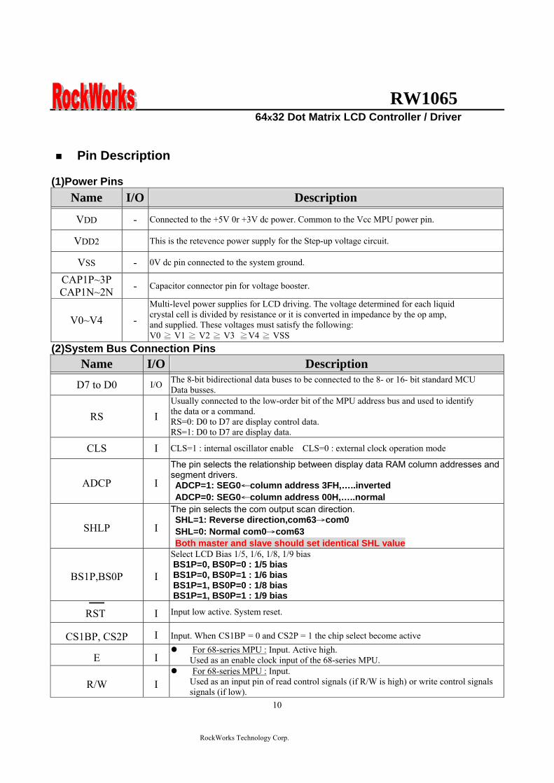
RW1065 64x32 Dot Matrix LCD Controller Driver
RockWorks Technology Corp
10
Pin Description
(1)Power Pins
Name IO Description
VDD - Connected to the +5V 0r +3V dc power Common to the Vcc MPU power pin
VDD2 This is the retevence power supply for the Step-up voltage circuit
VSS - 0V dc pin connected to the system ground
CAP1P~3P CAP1N~2N - Capacitor connector pin for voltage booster
V0~V4 - Multi-level power supplies for LCD driving The voltage determined for each liquid crystal cell is divided by resistance or it is converted in impedance by the op amp and supplied These voltages must satisfy the following V0 ≧ V1 ≧ V2 ≧ V3 ≧V4 ≧ VSS
(2)System Bus Connection Pins Name IO Description
D7 to D0 IO The 8-bit bidirectional data buses to be connected to the 8- or 16- bit standard MCU Data busses
RS I Usually connected to the low-order bit of the MPU address bus and used to identify the data or a command RS=0 D0 to D7 are display control data RS=1 D0 to D7 are display data
CLS I CLS=1 internal oscillator enable CLS=0 external clock operation mode
ADCP I
The pin selects the relationship between display data RAM column addresses and segment drivers ADCP=1 SEG0larrcolumn address 3FHhellipinverted ADCP=0 SEG0larrcolumn address 00Hhellipnormal
SHLP I
The pin selects the com output scan direction SHL=1 Reverse directioncom63rarrcom0 SHL=0 Normal com0rarrcom63 Both master and slave should set identical SHL value
BS1PBS0P I
Select LCD Bias 15 16 18 19 bias BS1P=0 BS0P=0 15 bias BS1P=0 BS0P=1 16 bias BS1P=1 BS0P=0 18 bias BS1P=1 BS0P=1 19 bias
RST ―
I Input low active System reset
CS1BP CS2P I Input When CS1BP = 0 and CS2P = 1 the chip select become active
E I For 68-series MPU Input Active high
Used as an enable clock input of the 68-series MPU
RW I For 68-series MPU Input
Used as an input pin of read control signals (if RW is high) or write control signals signals (if low)
RW1065 64x32 Dot Matrix LCD Controller Driver
RockWorks Technology Corp
11
(3)LCD Driver Circuit Signals
Name IO Description
CLL IO
Inputoutput IO selection
MS = ldquoHrdquo amp CLS = ldquoHrdquo Output MS = ldquoLrdquo amp CLS = ldquoHrdquo Input MS = ldquoXrdquo amp CLS = ldquoLrdquo Input
This is a display data latch signal to count up the line counter and common counterat each signal falling and rising edges
SEGn O Output A single level of V0 V2 V3 and VSS is selected by the combination of display RAM contents and FR signal
COMn O Output The output pin for LCD common (row) driving A single level of V0 V1 V4 and VSS is selected by the combination of common counter output and FR signal The slave LSI has the reverse common output scan sequence than the master LSI
FRR IO
Inputoutput This is the liquid crystal alternating current signal IO terminal lO selection
MS = ldquoHrdquoOutput MS = ldquoLrdquoInput
VRAB I Provides the voltage between V0 and VSS through a resistive voltage divider
MS I
Input The master or slave LSI operation select pin for the RW1065
MS OperatingMode FR CL V0~V4 Power
SupplyInternal
OSC COMMON
Output SEG
output
High Master Output See CLS On On See
CLS COM0-31 SEG0-63
Low Slave Input Input Off Off Off COM32-63
SEG64-127
RW1065 64x32 Dot Matrix LCD Controller Driver
RockWorks Technology Corp
12
DESCRIPTION OF FUNCTIONS
The Parallel Interface (6800 series MPU)
Shared 6800 Series
RS RW Function
1 1 Reads the display data
1 0 Writes the display data
0 1 Status read
0 0 Write control data (command)
The Chip Select The RW1065 Series chips have two chip select terminals CS1
―BP and CS2P
When the chip select is inactive D0 to D7 enter a high impedance state and the RS E and RW inputs are inactive
The Accessing the Display Data RAM and the Internal Registers Data transfer at a higher speed is ensured since the MPU is required to satisfy the cycle time (tCYC) requirement alone in accessing the RW1065 Series Wait time may not be considered And in the RW1065 Series chips each time data is sent from the MPU a type of pipeline process between LSIs is performed through the bus holder attached to the internal data bus Internal data bus For example when the MPU writes data to the display data RAM once the data is stored in the bus holder then it is written to the display data RAM before the next data write cycle Moreover when the MPU reads the display data RAM
the first data read cycle (dummy) stores the read data in the bus holder and then the data is read from the bus holder to the system bus at the next data read cycle There is a certain restriction in the read sequence of the display data RAM Please be advised that data of the specified address is not generated by the read instruction issued immediately after the address setup This data is generated in data read of the second time Thus a dummy read is required whenever the address setup or write cycle operation is conducted This relationship is shown in Figure 2
RW1065 64x32 Dot Matrix LCD Controller Driver
RockWorks Technology Corp
13
E
Fig 2b read timing
E
RW
Fig 2a write timing (RW=rdquoLrdquo)
RS
RS
RW1065 64x32 Dot Matrix LCD Controller Driver
RockWorks Technology Corp
14
Display Data RAM The display data RAM is a RAM that stores the dot data for the display It has a 64 (8 page x 8 bit) x 64 bit structure It is possible to access the desired bit by specifying the page address and the column addressBecause as is shown in Figure 3 the D7 to D0 display data from the MPU corresponds to the liquid crystal display common direction there are few constraints at the time of display data transfer when multiple RW1065 series chips are used
thus and display structures can be created easily and with a high degree of freedom Moreover reading from and writing to the display RAM from the MPU side is performed through the IO buffer which is an independent operation from signal reading for the liquid crystal driver Consequently even if the display data RAM is accessed asynchronously during liquid crystal display it will not cause adverse effects on the display (such as flickering)
0
1
0
0
1
1
0
0
1
0
1
0
0
1
0
1
0
0
1
0
0
0
0
0
0
D0
D1
D2
D3
D4
-
Display data RAM Liquid crystal display
COM0
COM1
COM2
COM3
COM4
-
Figure3
The Page Address Circuit As shown in Figure 4 page address of the display data RAM is specified through the Page Address Set Command The page address must be specified again when changing pages to perform access
The Column Address As is shown in Table 4 the display data RAM column address is specified by the Column Address Set command The specified column address is incremented (+1) with each display data readwrite command This allows the MPU display data to be accessed continuously Moreover the increment of column addresses stops with 3FH Because the column address is independent of the page address when moving for example from page 0 column 3FH to page 1
column 00H it is necessary to respecify both the page address and the column address Furthermore as is shown in Table 4 the ADC command (segment driver direction select command) can be used to reverse the relationship between the display data RAM column address and the segment output Because of this the constraints on the IC layout when the LCD module is assembled can be minimized
Table 4 SEG Output
ADC set SEG0 SEG 63
ADC(D0)=0 0 rarr Column Address rarr 63 ADC(D0)=1 63 larr Column Address larr 0
RW1065 64x32 Dot Matrix LCD Controller Driver
RockWorks Technology Corp
15
Figure 4
Page Address D3 D2 D1 D0
DataSE
G0
SEG
1
SEG
2
SEG
3
SEG
4
SEG
5
SEG
6
SEG
7
SEG
8
helliphelliphelliphellip
SEG
55
SEG
56
SEG
57
SEG
58
SEG
59
SEG
60
SEG
61
SEG
62
SEG
63 SEG
COM
D0 COM0
D1 COM1
D2 COM2
D3 COM3
D4 COM4
D5 COM5
D6 COM6
0 0 0 0
D7
Page 0
COM7
D0 COM8
D1 COM9
D2 COM10
D3 COM11
D4 COM12
D5 COM13
D6 COM14
0 0 0 1
D7
Page 1
COM15
D0 COM16
D1 COM17
D2 COM18
D3 COM19
D4 COM20
D5 COM21
D6 COM22
0 0 1 0
D7
Page 2
COM23
D0 COM24
D1 COM25
D2 COM26
D3 COM27
D4 COM28
D5 COM29
D6 COM30
0 0 1 1
D7
Page 3
COM31
ADC=0 00
01
02
03
04
05
06
07
08
helliphelliphelliphellip 55
56
57
58
59
60
61
62
63
COLUMN ADC=1 63
62
61
60
59
58
57
56
55
helliphelliphelliphellip 08
07
06
05
04
03
02
01
00
RW1065 64x32 Dot Matrix LCD Controller Driver
RockWorks Technology Corp
16
Common Timing Generator Circuit Display Data Latch Circuit Generates common timing signals and FR frame signals from the CL basic clock The 132 or 164 duty (for RW1065) can be selected by the Duty Select command The 132 and 164 duties are provided by two chips consisting of the master and slave chips in the common multi-chip mode
This latch stores one line of display data for use by the LCD driver interface circuitry The output of this latch is controlled by the Display ONOFF
132 duty
164 duty
SHL=0
SHL=1
SHL=0
SHL=1
RW1065 64x32 Dot Matrix LCD Controller Driver
RockWorks Technology Corp
17
Display Timing Generator Circuit
The display timing generator circuit generates the timing signal to the line address circuit and the display data latch circuit using the display clock The display data is latched into the display data latch circuit synchronized with the display clock and is output to the data driver output terminal Reading to the display data liquid crystal driver circuits is completely independent of accesses to the display data RAM by the MPU Consequently even if the display data
RAM is accessed asynchronously during liquid crystal display there is absolutely no adverse effect (such asflickering) on the display Moreover the display timing generator circuit generates the common timing and the liquid crystal alternating current signal (FR) from the display clock It generates a drive wave form using a 2 frame alternating current drive method as is shown in Figure 5 for the liquid crystal drive circuit
Two-frame alternating current drive waveform
Figure 5
When multiple RW1065 Series chips are used the slave chip must be supplied the display timing signals(FR CL) from the master chip
Table 5 shows the status of the FR and CL signals
Table 5 Operating Mode FR CL
Master (MS = ldquoHrdquo) The internal oscillator circuit is enabled (CLS = ldquoHrdquo) The internal oscillator circuit is disabled (CLS = ldquoLrdquo)
Output Output
Output Input
Slave (MS = ldquoLrdquo) The internal oscillator circuit is enabled (CLS = ldquoHrdquo) The internal oscillator circuit is disabled (CLS = ldquoLrdquo)
Input Input
Input Input
RW1065 64x32 Dot Matrix LCD Controller Driver
RockWorks Technology Corp
18
The Liquid Crystal Driver Circuits
These are a 64-channel (RW1065) that generate four voltage levels for driving the liquid crystal The combination of the display data the COM scan signal and the FR signal
produces the liquid crystal drive voltage output Figure 6 shows examples of the SEG and COM output waveform
Figure 6
RW1065 64x32 Dot Matrix LCD Controller Driver
RockWorks Technology Corp
19
The Power Supply Circuit
The power supply circuits are low-power consumption power supply circuits that generate the voltage levels required for the liquid crystal drivers They comprise Booster circuits and voltage follower circuits They are only enabled in master operation The power supply circuits can turn on automatically after power on
Consequently it is possible to make an external power supply and the internal power supply function somewhat in parallel
The Liquid Crystal Voltage Generator Circuit The V0 voltage is produced by a resistive voltage divider outside the IC through VRAB pin and can be produced at the V1 V2 V3 and V4 voltage levels required for liquid crystal driving Moreover when the voltage follower changes the impedance it provides V1 V2 V3 and V4 to the liquid crystal drive circuit 15 bias or 16 bias or 18 bias or 19 bias for RW1065 can be selected by BS0 and BS1 pins V0-Vss maximum voltage is 15V Vout-Vss maximum voltage is 17V If VDD lt 35V it can use the Booster circuit 2x3x4xThe booster voltage can follow the spec condition (Vout-Vss ≦ 17V max voltage) if VDD gt35V only use the 2X3X booster circuit that can ensure the V0-Vss voltage ≦ 15V If use the VDD voltage 5V and 4X booster itrsquos over the spec operation condition To turn on built-in power (boosterfollower) must waiting 200mS to display on for boosterfollower stable Therefore power off must follower ldquopower off sequencerdquo too
Power on Display off
Power off
Power off sequence
Wait time gt200mS
Display on
Power on sequence
RW1065 64x32 Dot Matrix LCD Controller Driver
RockWorks Technology Corp
20
The Reset Circuit
When the RTP input comes to the ldquoLrdquo level these LSIs return to the default state Their default states are as follows 1 Display OFF 2 Display all point on is select to normal 3 Display normalreverse is select to normal 4 164 duty is selected 5 Read modify write OFF 6 Column address set to Address 0 7 Page address set to Page 0 8 Start line set to first line 9 Frame frequency set to default 10 Power save mode released 11 Ext set to ldquo0rdquo When the power is turned on the IC internal state becomes unstable and it is necessary to initialize it using the RSTP terminal After the initialization each input terminal should be controlled normally While RSTP is ldquoLrdquo the oscillator works but the display timing generator stops and the CL FR terminals are fixed to ldquoHrdquo The terminals D0 to D7 are not affected
RW1065 64x32 Dot Matrix LCD Controller Driver
RockWorks Technology Corp
21
TABLE OF RW1065 INSTRUCTIONS
Instruction code Instruction RS RW DB7 DB6 DB5 DB4 DB3 DB2 DB1 DB0 Description
EXT=0 or 1
MODE SET 0 0 0 0 0 0 1 1 0 EXT Set EXT mode
Instruction code Instruction RS RW DB7 DB6 DB5 DB4 DB3 DB2 DB1 DB0 Description
EXT=0 Display ONOFF 0 0 0 0 1 1 1 1 1 D D=0Display OFF
D=1Display ONSet page address 0 0 1 0 1 1 1 P2 P1 P0 Set page address
Set column address 0 0 0 1 Y5 Y4 Y3 Y2 Y1 Y0 Set column
address MSB
Read Status 0 1 BUSY 0 ON OFF RESET 0 0 0 0 Read register
status Write display
data 1 0 Write data Write data into DDRAM
Read display data 1 1 Read data Read data from
DDRAM Set initial
display line register
0 0 1 1 S5 S4 S3 S2 S1 S0 Specify the initial
display line to realize vertical scrolling
Instruction code Instruction RS RW DB7 DB6 DB5 DB4 DB3 DB2 DB1 DB0 Description
EXT=1
NOP 0 0 0 0 0 0 0 0 0 0 no operation
Set modiy-read 0 0 0 0 0 0 1 0 0 0 Set modiy-read
mode
END 0 0 0 0 0 0 1 1 1 0 release modiy-read mode
Set power save mode 0 0 0 0 0 0 0 0 1 PSAVE P=0 normal mode
P=1 sleep mode
0 0 0 0 0 1 0 1 Display
COMMAND (double
command)
0 0 FRSEL
0 0 0 0 REV ALLON DUTY
DUTY=1 64 duty DUTY=0 32 duty ALLON=1display all on ALLON=0display
normal REV=1display reverse REV=0display normal FRSEL=1FR frequency double default FRSEL=0FR frequency default
RW1065 64x32 Dot Matrix LCD Controller Driver
RockWorks Technology Corp
22
Command Description
See the Table of RW1065 instructions The RW1065 series identifies a data bus using a combination of RS E and RW signals As the MPU translates a command in the internal timing only (independent from the external clock) its speed is very high The busy check is usually not required
Display ONOFF
EXT RS RW D7 D6 D5 D4 D3 D2 D1 D0
0 0 0 0 0 1 1 1 1 1 D
This command turns the display on and off D=1 Display ON D=0 Display OFF(default)
Set page Address This command specifies the page address that corresponds to the low address of the display data RAM when it is accessed by the MPU Any bit of the display data RAM can be accessed when its page address and column address are specified The display status is not changed even when the page address is changed
EXT RS RW D7 D6 D5 D4 D3 D2 D1 D0
0 0 0 1 0 1 1 1 A2 A1 A0
This command loads the page address register
A2 A1 A0 Page
0 0 0 0 (default)
0 0 1 1 0 1 0 2 0 1 1 3 1 0 0 4 1 0 1 5 1 1 0 6 1 1 1 7
Page mapping see Figure 4
RW1065 64x32 Dot Matrix LCD Controller Driver
RockWorks Technology Corp
23
Set Column Address This command specifies a column address of the display data RAM When the display data RAM is accessed by the MPU continuously the column address is incremented by I each time it is accessed from the set address Therefore the MPU can access to data continuously The column address stops to be incremented at address 63 and the page address is not changed continuously
EXT RS RW D7 D6 D5 D4 D3 D2 D1 D0
0 0 0 0 1 A5 A4 A3 A2 A1 A0
A5 A4 A3 A2 A1 A0 Column Address0 0 0 0 0 0 0(default) 0 0 0 0 0 1 1
1 1 1 1 1 1 63
Read Status
EXT RS RW D7 D6 D5 D4 D3 D2 D1 D0
0 0 1 BUSY 0 ON OFF RESET 0 0 0 0
The BUSY Flag bit indicates that RW 1065 is operating or no operating
BUSY=1 Operation BUSY=0 Ready
The ONOFF bit indicates the current status of the display It is the inverse of the polarity of the display ONOFF command ONOFF=1 Display OFF ONOFF=0 Display ON The RESET bit indicates whether the driver is executing a hardware or software reset or if it is in normal operating mode RESET=1 Currently executing reset command RESET=0 Normal operation
RW1065 64x32 Dot Matrix LCD Controller Driver
RockWorks Technology Corp
24
Write Display Data
EXT RS RW D7 D6 D5 D4 D3 D2 D1 D0
0 1 0 Write data
Writes 8-bits of data into the display data RAM at a location specified by the contents of the column address and page address registers and then increments the column address register by one
Read Display Data
EXT RS RW D7 D6 D5 D4 D3 D2 D1 D0
0 1 1 Read data
Reads 8-bits of data from the data IO latch updates the contents of the IO latch with display data from the display data RAM location specified by the contents of the column address and page address registers and then increments the column address register After loading a new address into the column address register one dummy read is required before valid data is obtained
Set initial display line register
EXT RS RW D7 D6 D5 D4 D3 D2 D1 D0
0 0 0 1 1 S5 S4 S3 S2 S1 S0
Loads the RAM line address of the initial display line COM 0 into the initial display line register The RAM display data becomes the top line of the LCD screen It is followed by the higher number lines in ascending order corresponding to the duty cycle The screen can be scrolled using this command by incrementing the line address(default value=rdquo00Hrdquo)
RW1065 64x32 Dot Matrix LCD Controller Driver
RockWorks Technology Corp
25
Read-Modify-Write
EXT RS RW D7 D6 D5 D4 D3 D2 D1 D0
1 0 0 0 0 0 0 1 0 0 0
This command defeats column address register auto-increment after data reads The current contents of the column Address register are saved The mode remains active until an End command is received When the End command is entered the column address is returned to the one used during input of Read-Modify-Write Command This function can reduce the load of MPU when data change is repeated as a specific display area Any command other than Data Read or Write can be used in the Read-Modify-Write mode However the Column Address Set command cannot be used
End
EXT RS RW D7 D6 D5 D4 D3 D2 D1 D0
1 0 0 0 0 0 0 1 1 1 0
This command cancels read-modify-write mode and restores the contents of the column address register to their value prior to the receipt of the Read-Modify-Write command
N N+1 N+2 N+3 N+m N
Read -modify-write mode set End
Returm
Column address
Set page address
Set column address
Read-modify-write
Dummy read
Read data
Write data
End
CompletedNo
Yes
RW1065 64x32 Dot Matrix LCD Controller Driver
RockWorks Technology Corp
26
Set power save mode
EXT RS RW D7 D6 D5 D4 D3 D2 D1 D0
1 0 0 0 0 0 0 0 0 1 PSAVE
When power save mode is entered thus greatly reducing power consumption In the power save mode the display data is saved as is the operating mode that was in effect before the power saver mode was initiated and the MPU is still able to access the display data RAM PSAVE=1 Sleep mode PSAVE=0 Normal mode Sleep mode This stops all operations in the LCD display system and as long as there are no accesses from the MPU the consumption current is reduced to a value near the static current The internal modes during sleep mode are as follows 1 The oscillator circuit and the LCD power supply circuit are halted 2 All liquid crystal drive circuits are halted and the segment and common drive outputs output a Vss level
Display command double command
EXT RS RW D7 D6 D5 D4 D3 D2 D1 D0
1 0 0 0 0 0 0 0 1 0 1
1 0 0 FRSEL 0 0 0 0 REV ALLON DUTY
Display NormalReverse set REV=1 Reverse REV=0 Normal(default) Display All Point ONOFF ALLON=1 All display points ON ALLON=0 Normal(default) Select Duty Duty=1 164 duty cycle(default) Duty=0 132 duty cycle FRAME FREQUENCY Select FRSEL=1 Double FRSEL=0 (default)
RW1065 64x32 Dot Matrix LCD Controller Driver
RockWorks Technology Corp
27
Hardware Pin Set
Select ADC by ADC Pin The pin selects the relationship between display data RAM column addresses and segment drivers ADC=1 SEG0larrcolumn address 3FHhellipinverted ADC=0 SEG0larrcolumn address 00Hhellipnormal(default) This command is provided to reduce restrictions on the placement of driver ICs and routing of traces during printed circuit Board design See Figure 4 for a table of segments and column addresses for the two values of D
Select SHL by SHL Pin The pin selects the com output scan direction SHL=1 Reverse directioncom63rarrcom0 SHL=0 Normal com0rarrcom63 Both master and slave should set identical SHL value
Select LCD Bias by BS0 BS1 Pin
BS1 BS0 Bias 0 0 15 bias 0 1 16 bias 1 0 18 bias 1 1 19 bias
RW1065 64x32 Dot Matrix LCD Controller Driver
RockWorks Technology Corp
28
When an External Resistance is Used The liquid crystal power supply voltage V0 is set by adding resistors Rarsquo and Rbrsquo between VDD and VR and between VR and V0 respectively
RW1065
RW1065 64x32 Dot Matrix LCD Controller Driver
RockWorks Technology Corp
29
The set voltage circuits
Using the step-up voltage circuits equipped within the RW1065 chips it is possible to produce a 2X 3X 4X step-up voltage levels 2X step-up
To produce voltage level in the positive direction at the Vout terminal that is 2 times the voltage difference between VSS and VDD2 Please configure set voltage circuits like this Place a 1uF~22uF capacitor between CAP1N and CAP1P Place a 1uF~22uF capacitor between VSS and VOUT Short CAP2P CAP3P and VOUT Leave CAP2N open 3X step-up
To produce voltage level in the positive direction at the Vout terminal that is 3 times the voltage difference between VSS and VDD2 Please configure set voltage circuits like this Place a 1uF~22uF capacitor between CAP1N and CAP1P Place a 1uF~22uF capacitor between VSS and VOUT Place a 1uF~22uF capacitor and 100 ohms resistor between CAP2N and CAP2P Short CAP3P and Vout 4X step-up
To produce voltage level in the positive direction at the Vout terminal that is 4 times the voltage difference between VSS and VDD2 Please configure set voltage circuits like this Place a 1uF~22uF capacitor between CAP1N and CAP1P Place a 1uF~22uF capacitor between VSS and VOUT Place a 1uF~22uF capacitor and 100 ohms resistor between CAP2N and CAP2P Place a 1uF~22uF capacitor and 100 ohms resistor between CAP1N and CAP3P
RW1065 64x32 Dot Matrix LCD Controller Driver
RockWorks Technology Corp
30
ABSOLUTE MAXIMUM RATINGS Characteristics Symbol Value Unit
Power supply voltage VDD -03 to +70 V
LCD driver voltage Vout 0 to +17 V
Input voltage VIN -03 to VDD+03 V
Operating temperature TA -40 to +85
Storage temperature TSTO -55 to +125
DC CHARACTERISTICS
Rating Item Symbol Condition Min Typ Max Unit ApplicablePin
Operating Voltage VDD - 27 30 55 V VDD1
Step up output voltage Vout (Relative to VDD) 0 - 17 V Vout
Voltage follower circuit operating Voltage V0 (Relative to VDD) 0 - 15 V V0
V0 accuracy V0 - 0 - 15 V0
High-level Input Voltage Low-level Input Voltage
VIHC VILC - 07 VDD
Vss - VDD 09 V 2
High-level Output Voltage Low-level Output Voltage
VOHC VOLC
IOH = ndash05 mA IOL = 05 mA
08VDD Vss - VDD
02 VDD V 3
Input leakage current ILI VIN = VDD or VSS -1 - 2 uA 4
Output leakage current ILO - -1 1 uA 5
Liquid Crystal Driver ON Resistance RON
Ta= 25degC(Relative To VDD)
V0 =15 V - 16 20 KΩ SEGn COMn 6
Internal Oscillator fOSC 2286 254 2794 Oscillator
Frequency External Input RECOMMAND fCL
Ta = 25degC 132Duty 2286 254 2794
kHz CL
Internal Oscillator fOSC 45 5 55 Oscillator
Frequency External Input RECOMMAND fCL
Ta = 25degC 164Duty 45 5 55
kHz CL
bullDynamic Consumption Current During Display with the Internal Power Supply OFF Current consumed by total ICs when an external power supply is used
Unless otherwise specified Vss=0V VDD=30V
RW1065 64x32 Dot Matrix LCD Controller Driver
RockWorks Technology Corp
31
Display Pattern OFF
Ta = 25degC Vout=17V Rating Item Symbol Condition Min Typ Max Unit Notes
VDD=30 V V0-Vss=8V - 10 15 RW1065 IDD VDD=50 V V0-Vss=8V - 35 45
microA 7
Display Pattern Checker
Ta = 25degC Vout=17V Rating Item Symbol Condition Min Typ Max Unit Notes
VDD=30 V V0-Vss=8V - 15 20 RW1065 IDD VDD=50 V V0-Vss=8V - 40 50
microA 7
Display Pattern OFF
Ta = 25degC Vout=17V Rating Item Symbol Condition Min Typ Max Unit Notes
VDD=30 V V0-Vss=8V - 15 20 RW1065 IDD VDD=50 V V0-Vss=8V - 40 50
microA 7
Display pattern Checker
Ta = 25degC Vout=17V Rating Item Symbol Condition Min Typ Max Unit Notes
VDD=30 V V0-Vss=8V - 65 80 RW1065 IDD VDD=50 V V0-Vss=8V - 130 150
microA 7
bull Consumption Current at Time of Power Saver Mode VSS = 0 V VDD = 30 V plusmn 10
Rating Item Symbol Condition Min Typ Max Unit Notes
Sleep mode IDD - - 5 10 microA -
References for items market with 1 While a broad range of operating voltages is guaranteed performance cannot be guaranteed if there are sudden fluctuations to the
voltage while the MPU is being accessed 2 The RS D0 to D5 D6 D7 E RW CS1BP CS2P CLS CL FR MS and RST
― terminals
3 The D0 to D7 FR and CL terminals 4 The RS E RW CS1BP CS2P CLS MS and RST
― terminals
5 Applies when the D0 to D5 D6 D7 CL and FR terminals are in a high impedance state 6 These are the resistance values for when a 01 V voltage is applied between the output terminals SEGn or COMn and
the various power supply terminals (V1 V2 V3 and V4) These are specified for the operating voltage (3) range RON = 01 V ∆I (Where ∆I is the current that flows when 01 V is applied while the power supply is ON)
7 It indicates the current consumed on ICs alone when the internal oscillator circuit and display are turned on Does not include the current due to the LCD panel capacity and wiring capacity Applicable only when there is no access from the MPU
RW1065 64x32 Dot Matrix LCD Controller Driver
RockWorks Technology Corp
32
TIMING CHARACTERISTICS
68 Interface
(Ta=-40 to 85 degC) VDD=27 to 45V
Rating VDD=45 to 55V
Rating Item Signal Symbol ConditionMin Max Min Max
Units
Address hold time RS tAH6 0 mdash 0 mdash Address setup time RS tAW6
mdash 0 mdash 0 mdash
ns
System cycle time RS tCYC6 mdash 900 mdash 800 mdash ns Data setup time D0 to D7 tDS6 100 mdash 100 mdash Data hold time D0 to D7 tDH6
mdash 0 mdash 0 mdash
ns
Access time D0 to D7 tACC6 mdash 350 mdash 250
Output disable time D0 to D7 tOH6 CL = 100 pF
mdash 300 mdash 200 ns
Read tEWHR 360 mdash 300 mdash Enable H pulse time
WriteE
tEWHW mdash
360 mdash 300 mdash ns
Read tEWLR 450 mdash 400 mdash Enable L pulse time
WriteE
tEWLW mdash
450 mdash 400 mdash ns
1 All timing is specified using 20 and 80 of VDD as the reference 2 tEWLW and tEWLR are specified as the overlap between CS1BP being ldquoLrdquo (CS2P = ldquoHrdquo) and E
RW1065 64x32 Dot Matrix LCD Controller Driver
RockWorks Technology Corp
33
Reset Timing
Rating Item Signal Symbol Condition
Min Typ Max Units
Reset time mdash tR mdash mdash - 2 micros
Reset ldquoLrdquo pulse width RST tRW mdash 2 - mdash micros
1 When double chip was be used then the duty set command must be set between the tR
RW1065 64x32 Dot Matrix LCD Controller Driver
RockWorks Technology Corp
34
IO PAD CONFIGURATION
RW1065 64x32 Dot Matrix LCD Controller Driver
RockWorks Technology Corp
35
THE MPU INTERFACE (REFERENCE EXAMPLES) The RW1065 Series can be connected to 6800 Series MPUs The display area can be enlarged by using multiple RW1065 Series chips When this is done the chip select signal can be used to select the individual ICs to access
6800 Series MPUs
RW
106
5
RW1065 64x32 Dot Matrix LCD Controller Driver
RockWorks Technology Corp
36
When using external multi-level power supply for LCD driving (REFERENCE EXAMPLE)
Using a resistor divider can provide RW1065 external multi-level power supply for LCD driving
The circuit below shows a resistor divider network which can bias V0 V1 V2 V3 and V4 externally
RW1065 64x32 Dot Matrix LCD Controller Driver
RockWorks Technology Corp
37
bullWhen V0 V1 V2 V3 and V4 are biased by external power supply analog section of RW1065 should be turn off by software during LCD initialization The example in below shows the sequence to turn off analog section when external bias is used Begin of LCD initialization 1 Reset RW1065 2 SET EXT=1 (mode instruction)
RS RW DB7 DB6 DB5 DB4 DB3 DB2 DB1 DB00 0 0 0 0 0 1 1 0 1
3 SET Display Command (double command)
RS RW DB7 DB6 DB5 DB4 DB3 DB2 DB1 DB00 0 0 0 0 0 0 1 0 1 0 0 0 0 1 1 0 0 0 1
4 SET EXT=1 (mode instruction)
RS RW DB7 DB6 DB5 DB4 DB3 DB2 DB1 DB00 0 0 0 0 0 1 1 0 0
End of LCD initialization
bullBecause pins can not set LCD bias when external power supplies are used for LCD driving the bias can be set by an appropriate configuration for a resistor voltage divider networks The example is shown below
VSS
R
R
NR
R
R
RV1
RV2
RV3
RV4
V0
Bias Network Circuit Concept 15 Bias N=1 total = 5R 16 Bias N=2 total =6R 18 Bias N=4 total =8R 19 Bias N=5 total = 9R
RW1065 64x32 Dot Matrix LCD Controller Driver
RockWorks Technology Corp
38
Single chip solution for RW1065 application (REFERENCE EXAMPLE)
For a 64x32 application the duty cycle of LCD panel is 164 and the display duty of RW1065 should be set to 164 The display duty cycle can be selected by the DUTY bit in display command The diagram for 64x32 application is shown below
64 SEGx32COM LCD Panel
164 duty cycle
RW1065 DUTY=1
COM1~33
SEG1~65
RW1065 64x32 Dot Matrix LCD Controller Driver
RockWorks Technology Corp
39
Using an adjustable resistor on the main board to adjust the contrast of liquid crystal display (REFERENCE EXAMPLE)
The schematic shows an adjustable resistor on main board that can adjust voltage level of V0
RW1065 64x32 Dot Matrix LCD Controller Driver
RockWorks Technology Corp
40
Package information (Please pay close attention to the information in this section Do not hesitate to consult with our sale representative if you have any question or concern)
In order to make better bonding yield for RW1065 please follow the tips and recommendations in this section In this section few tips about COB footprint style PCB layout and wire bonding will be discussed
The drawing in below shows the PCB footprint style which we recommend for RW1065 Pads array in
curve shape is easier for Al wire bonding Besides that a real size COB footprint for RW1065 is also shown in below RW1065 COB footprint is also available in powerpcb or protel format for design reference purpose
The ratio is 11
RW1065 64x32 Dot Matrix LCD Controller Driver
RockWorks Technology Corp
41
During COB footprint design there have some tips about footprint that the PCB designer should know The angle between bonding wire and vertical line should less than 45 Otherwise the wire shorts would become very easy to happen at fours corners of the chip
The angle between bonding wire and vertical line could be reduced by expanding the distance between pads array and the chip In addition reducing length in horizon direction of pads array could minimize the angle between bonding wire and vertical line The picture in below will help to illustrate this concept From the experiences COB footprint style affects the bonding yield
Bad Wires are too close to each other
The angle between bonding wire and vertical line is greater than 45
The angle between bonding wire and vertical line is less than 45
Wires are not too close to each other
Reducing length in horizon direction of pads array could minimize the angle between bonding wire and vertical line
The angle between bonding wire and vertical line could be reduced by expanding the distance between pads array and the chip
RW1065 64x32 Dot Matrix LCD Controller Driver
RockWorks Technology Corp
42
If the gap between pads of COB footprint is filled with solder mask coating it is difficult to bond Al wire to
the pads The top solder masks layer that overlap COB footprint area should be removed
Please use 1 mils diameter Al wire for RW1065 wire bonding
1 2 3 4 5 6
A
B
C
D
654321
D
C
B
A
Title
Number RevisionSize
C
Date 29-Aug-2007 Sheet of File D公司資料99seMyDesignddb Drawn By
RW1065
COM131
COM142
COM153
COM164
COM175
COM186
COM197
COM208
COM219
COM2210
COM2311
COM2412
COM2513
COM2614
COM2715
COM2816
COM2917
COM3018
COM3119
SEG
6320
SEG
6221
SEG
6122
SEG
6023
SEG
5924
SEG
5825
SEG
5726
SEG
5627
SEG
5528
SEG
5429
SEG
5330
SEG
5231
SEG
5132
SEG
5033
SEG
4934
SEG
4835
SEG
4736
SEG
4637
SEG
4538
SEG
4439
SEG
4340
SEG
4241
SEG
4142
SEG
4043
SEG
3944
SEG
3845
SEG
3746
SEG
3647
SEG
3548
SEG
3449
SEG
3350
SEG
3251
SEG
3152
SEG
3053
SEG
2954
SEG
2855
SEG
2756
SEG
2657
SEG
2558
SEG
2459
SEG
2360
SEG
2261
SEG
2162
SEG
2063
SEG
1964
SEG
1865
SEG
1766
SEG
1667
SEG
1568
SEG
1469
SEG13 70SEG12 71SEG11 72SEG10 73SEG9 74SEG8 75SEG7 76SEG6 77SEG5 78SEG4 79SEG3 80SEG2 81SEG1 82SEG0 83ADCP 84CLL 85
VSS
86D
087
D1
88D
289
D3
90D
491
D5
92D
693
D7
94C
S1B
P95
CS2
P96
ERD
P97
AO
P(R
S)98
RW
RP
99V
DD
100
RST
P10
1C
LSP
102
FRR
103
MSP
104
BS1
P10
5B
S0P
106
SHLP
107
VD
D2
108
CA
P2N
109
CA
P2P
110
CA
P1P
111
CA
P1N
112
CA
P3P
113
VO
UT
114
V0
115
VR
AB
116
V3
117
V2
118
V4
119
V1
120
CO
M0
121
CO
M1
122
CO
M2
123
CO
M3
124
CO
M4
125
CO
M5
126
CO
M6
127
CO
M7
128
CO
M8
129
CO
M9
130
CO
M10
131
CO
M11
132
CO
M12
133
4897x1902 um
IC1
RW1065
C9CAPR4
100R0603
R30R0603
C8
CAP
C7
CAP
R2
100R0603
R1
0R0603C6 22uf
R50R
R6300R
R7RES1
R8NC R9
100R0603
VDD
R10
NC
R11
100R0603
R12
100R0603
R13
NC
R14
100R0603
R15
NC
VDD
D0
D1
D2
D3
D4
D5
D6
D7
DB[07]
VDDC5
01uf0603
VD
D
CS2
P
123456789
1011121314151617181920
J1
CON20
C1201uf0603
R3951K0603
VDD
CAP Value1UF~22UF
2XPut C6C8 Short R1R3Open R2R4C7C93XPut C6C8C9 R4Short R1Open R2R3C74XOpen R1R3
BS0 BS1 Bias0 0
0 1
1 0
11
15 bias
16 bias
18 bias
19 bias
ADC=0 SEG0lt~column address 00Hnormal(default) ADC=1 SEG0lt~column address 3FHinverted
SHL=0 Normal COM0~gtCOM63(default)SHL=1 Reverse direction COM63~gtCOM0
R16100R0603
LCD PANEL 64X32RockWorks
RW1065 64X32
COM0-31 SEG0-63SHL=0 ADC=0
SHL=1COM31-0
ADC=1SEG63-0
if use single chip for 32 command displaythe display command must select 164 dutyDisplay panel must select 164 duty type
VO
UT
C3P
C1N
C1P
C2P
C2N
VDD2
ADC
SHL
BS0
BS1
CLLADC
V1
V2
V3
V4
VR
AB
V0
VO
UT
C3P
C1N
C1P
C2P
C2N
VD
D2
SHL
BS0
BS1
FRR
RST
P
RW
RS
E CS1
B
CS1
V0RSRWED0D1D2D3D4D5D6D7
RSTPAK
C4
22uf
RBRES1
RA1RES1
C2
22uf
C1
22uf
C3
22uf
C0
22uf
R20
100k0603
R21
100k0603
R17
200K0603
V1
V2
V3
V4 VRAB
V0
V0
OPTION
B
R18
300R0603
RA2RES1
VADJ
R19100R
R23 RES1R22 0R
R24
RES1
R25
0R
VDD
CS1BP
CS2P
CS1
CS1
R26
22R0603
R27
22R0603
C1047uf
C11
01uf
VSS_INVDD_IN
D1DIODE
FGND
鐵框地
VSS
VDD
R28 10RR29 10RR30 10RR31 10RR32 10RR33 10RR34 10RR35 10RR36 10RR37 10RR38 10R
VADJ
1 2 3 4 5 6
A
B
C
D
654321
D
C
B
A
Title
Number RevisionSize
C
Date 29-Aug-2007 Sheet of File D公司資料99seMyDesignddb Drawn By
RW1065
COM131
COM142
COM153
COM164
COM175
COM186
COM197
COM208
COM219
COM2210
COM2311
COM2412
COM2513
COM2614
COM2715
COM2816
COM2917
COM3018
COM3119
SEG
6320
SEG
6221
SEG
6122
SEG
6023
SEG
5924
SEG
5825
SEG
5726
SEG
5627
SEG
5528
SEG
5429
SEG
5330
SEG
5231
SEG
5132
SEG
5033
SEG
4934
SEG
4835
SEG
4736
SEG
4637
SEG
4538
SEG
4439
SEG
4340
SEG
4241
SEG
4142
SEG
4043
SEG
3944
SEG
3845
SEG
3746
SEG
3647
SEG
3548
SEG
3449
SEG
3350
SEG
3251
SEG
3152
SEG
3053
SEG
2954
SEG
2855
SEG
2756
SEG
2657
SEG
2558
SEG
2459
SEG
2360
SEG
2261
SEG
2162
SEG
2063
SEG
1964
SEG
1865
SEG
1766
SEG
1667
SEG
1568
SEG
1469
SEG13 70SEG12 71SEG11 72SEG10 73SEG9 74SEG8 75SEG7 76SEG6 77SEG5 78SEG4 79SEG3 80SEG2 81SEG1 82SEG0 83ADCP 84CLL 85
VSS
86D
087
D1
88D
289
D3
90D
491
D5
92D
693
D7
94C
S1B
P95
CS2
P96
ERD
P97
AO
P(R
S)98
RW
RP
99V
DD
100
RST
P10
1C
LSP
102
FRR
103
MSP
104
BS1
P10
5B
S0P
106
SHLP
107
VD
D2
108
CA
P2N
109
CA
P2P
110
CA
P1P
111
CA
P1N
112
CA
P3P
113
VO
UT
114
V0
115
VR
AB
116
V3
117
V2
118
V4
119
V1
120
CO
M0
121
CO
M1
122
CO
M2
123
CO
M3
124
CO
M4
125
CO
M5
126
CO
M6
127
CO
M7
128
CO
M8
129
CO
M9
130
CO
M10
131
CO
M11
132
CO
M12
133
4897x1902 um
IC1
RW1065 Master
RW1065
COM131
COM142
COM153
COM164
COM175
COM186
COM197
COM208
COM219
COM2210
COM2311
COM2412
COM2513
COM2614
COM2715
COM2816
COM2917
COM3018
COM3119
SEG
6320
SEG
6221
SEG
6122
SEG
6023
SEG
5924
SEG
5825
SEG
5726
SEG
5627
SEG
5528
SEG
5429
SEG
5330
SEG
5231
SEG
5132
SEG
5033
SEG
4934
SEG
4835
SEG
4736
SEG
4637
SEG
4538
SEG
4439
SEG
4340
SEG
4241
SEG
4142
SEG
4043
SEG
3944
SEG
3845
SEG
3746
SEG
3647
SEG
3548
SEG
3449
SEG
3350
SEG
3251
SEG
3152
SEG
3053
SEG
2954
SEG
2855
SEG
2756
SEG
2657
SEG
2558
SEG
2459
SEG
2360
SEG
2261
SEG
2162
SEG
2063
SEG
1964
SEG
1865
SEG
1766
SEG
1667
SEG
1568
SEG
1469
SEG13 70SEG12 71SEG11 72SEG10 73SEG9 74SEG8 75SEG7 76SEG6 77SEG5 78SEG4 79SEG3 80SEG2 81SEG1 82SEG0 83ADCP 84CLL 85
VSS
86D
087
D1
88D
289
D3
90D
491
D5
92D
693
D7
94C
S1B
P95
CS2
P96
ERD
P97
AO
P(R
S)98
RW
RP
99V
DD
100
RST
P10
1C
LSP
102
FRR
103
MSP
104
BS1
P10
5B
S0P
106
SHLP
107
VD
D2
108
CA
P2N
109
CA
P2P
110
CA
P1P
111
CA
P1N
112
CA
P3P
113
VO
UT
114
V0
115
VR
AB
116
V3
117
V2
118
V4
119
V1
120
CO
M0
121
CO
M1
122
CO
M2
123
CO
M3
124
CO
M4
125
CO
M5
126
CO
M6
127
CO
M7
128
CO
M8
129
CO
M9
130
CO
M10
131
CO
M11
132
CO
M12
133
4897x1902 um
IC2
RW1065 Slave
C4
22uf
RBRES1
RA1RES1
C2
22uf
C1
22uf
C3
22uf
C0
22ufC9CAPR4
100R0603
R30R0603
C8
CAP
C7
CAP
R2
100R0603
R1
0R0603C6 22uf
R50R0603
R6300R0603
R7RES1
R8NC R9
100R0603
VDD
R10
NC
R11
100R0603
R12
NC
R13
100R0603
R14
100R0603
R15
NC
R16
100R0603
R17
NC
VDD
D0
D1
D2
D3
D4
D5
D6
D7
D0
D1
D2
D3
D4
D5
D6
D7
DB[07] DB[07]
VDDC10
01uf0603
VD
D
IC1_
CS2
P
VDD
IC2_
CS2
P
VD
D
C11
01uf0603
VSS
VSS
LCD PANEL 128X64
Master COM0-31 Slave COM32-63
Master SEG0-63 Slave SEG64-127
123456789
1011121314151617181920
J1
CON20
Master Slave
CAP Value1UF~22UF
2XPut C6C8 Short R1R3Open R2R4C7C93XPut C6C8C9 R4Short R1Open R2R3C74XOpen R1R3
RockWorksRW1065 128x64
BS0 BS1 Bias0 0
0 1
1 0
11
15 bias
16 bias
18 bias
19 bias
ADC=0 SEG0lt~column address 00Hnormal(default) ADC=1 SEG0lt~column address 3FHinverted
SHL=0 Normal COM0~gtCOM63(default)SHL=1 Reverse direction COM63~gtCOM0Both Master and Slave should set identical SHL value
SHL=0 SHL=0
ADC=0 ADC=0
Slave COM31-0
Slave SEG127-64
SHL=1
ADC=1
SHL=1Master COM63-32
ADC=1Master SEG63-0
R18100R0603
R22
100k0603
R23
100k0603
C501uF0603
R4551K0603
VDD
R19
200K0603
ADC1
ADC2
SHL
BS0
BS1
VDD2
V1
V2
V3
V4 VRAB
V0
V0V
OU
T
C3P
C1N
C1P
C2P
C2N
V1
V2
V3
V4
VR
AB
V0
VO
UT
C3P
C1N
C1P
C2P
C2N
VD
D2
SHL
BS0
BS1
FRR
RST
P
RW
RS
E IC1_
CS1
BP
V1
V2
V3
V4
VR
AB
V0
VO
UT
VD
D2
SHL
BS0
BS1
FRR
RST
P
RW
RS
E IC2_
CS1
BP
CLLADC1
CLLADC2
RSTP
CS1CS2
V0RSRWED0D1D2D3D4D5D6D7
AK
OPTION
R20
300R0603
RA2RES1
VADJ
R21
100R
B
R25 RESR24 0R
R26 RES R27 0RVDD
IC1_CS1BP
IC1_CS2P
CS1
CS1
R28 0R R29 RES
R30 RES R31 0R
IC2_CS1BP
IC2_CS2P
CS2
CS2
R32
22R0603
R33
22R0603
C1001uf
C11
47uf
D1DIODE
FGND
鐵框地
VSS
VDD
R34 10RR35 10RR36 10RR37 10RR38 10RR39 10RR40 10RR41 10RR42 10RR43 10RR44 10R
VSS_INVDD_IN
VADJ
VDD
1 2 3 4 5 6 7 8
A
B
C
D
87654321
D
C
B
A
Title
Number RevisionSize
D
Date 29-Aug-2007 Sheet of File D公司資料 99seMyDesignddb Drawn By
C422uf
RBRES1
RA1RES1
C3
22uf
C2
22uf
C1
22uf
C0
22ufC9CAPR4
100R0603
R30R0603
C8
CAP
C7
CAP
R2
100R0603
R1
0R0603C6 22uf
R220R0603
R23300R0603
R24RES1
R39
NCR40
100 ohm0603
VDD
R41
NC
R42
100 ohm0603
R43
NC
R44
100 ohm0603
R45
NC
R46
100 ohm0603
R47
100 ohm0603
R48
NC
R49
100 ohm0603
R50
NC
VDDCAP Value1UF~22UF
2XPut C6C8 Short R1R3Open R2R4C7C93XPut C6C8C9 R4Short R1Open R2R3C74XOpen R1R3
BS0 BS1 Bias0 0
0 1
1 0
11
15 bias
16 bias
18 bias
19 bias
ADC=0 SEG0lt~column address 00Hnormal(default)
ADC=1 SEG0lt~column address 3FHinverted
SHL=0 Normal COM0~gtCOM63(default)SHL=1 Reverse direction COM63~gtCOM0Both Master and Slave should set identical SHL value
R7
100k0603
R8
100k0603
V1
V2
V3
V4
V0
VRAB
V0
R5
200K
VDD2
VO
UT
C3P
C1N
C1P
C2P
C2N
ADC1
ADC2
ADC3
SHL
BS0
BS1
CS1CS2CS3
V0RSRWED0D1D2D3D4D5D6D7
RSTP
R3851K0603
C5
01uF
VDD
OPTION
R6
300R0603R9100R
RA2RES1
VADJ
RW1065
COM131
COM142
COM153
COM164
COM175
COM186
COM197
COM208
COM219
COM2210
COM2311
COM2412
COM2513
COM2614
COM2715
COM2816
COM2917
COM3018
COM3119
SEG
6320
SEG
6221
SEG
6122
SEG
6023
SEG
5924
SEG
5825
SEG
5726
SEG
5627
SEG
5528
SEG
5429
SEG
5330
SEG
5231
SEG
5132
SEG
5033
SEG
4934
SEG
4835
SEG
4736
SEG
4637
SEG
4538
SEG
4439
SEG
4340
SEG
4241
SEG
4142
SEG
4043
SEG
3944
SEG
3845
SEG
3746
SEG
3647
SEG
3548
SEG
3449
SEG
3350
SEG
3251
SEG
3152
SEG
3053
SEG
2954
SEG
2855
SEG
2756
SEG
2657
SEG
2558
SEG
2459
SEG
2360
SEG
2261
SEG
2162
SEG
2063
SEG
1964
SEG
1865
SEG
1766
SEG
1667
SEG
1568
SEG
1469
SEG13 70SEG12 71SEG11 72SEG10 73SEG9 74SEG8 75SEG7 76SEG6 77SEG5 78SEG4 79SEG3 80SEG2 81SEG1 82SEG0 83ADCP 84CLL 85
VSS
86D
087
D1
88D
289
D3
90D
491
D5
92D
693
D7
94C
S1B
P95
CS2
P96
ERD
P97
AO
P(R
S)98
RW
RP
99V
DD
100
RST
P10
1C
LSP
102
FRR
103
MSP
104
BS1
P10
5B
S0P
106
SHLP
107
VD
D2
108
CA
P2N
109
CA
P2P
110
CA
P1P
111
CA
P1N
112
CA
P3P
113
VO
UT
114
V0
115
VR
AB
116
V3
117
V2
118
V4
119
V1
120
CO
M0
121
CO
M1
122
CO
M2
123
CO
M3
124
CO
M4
125
CO
M5
126
CO
M6
127
CO
M7
128
CO
M8
129
CO
M9
130
CO
M10
131
CO
M11
132
CO
M12
133
4897x1902 um
IC1
RW1065 Master
RW1065
COM131
COM142
COM153
COM164
COM175
COM186
COM197
COM208
COM219
COM2210
COM2311
COM2412
COM2513
COM2614
COM2715
COM2816
COM2917
COM3018
COM3119
SEG
6320
SEG
6221
SEG
6122
SEG
6023
SEG
5924
SEG
5825
SEG
5726
SEG
5627
SEG
5528
SEG
5429
SEG
5330
SEG
5231
SEG
5132
SEG
5033
SEG
4934
SEG
4835
SEG
4736
SEG
4637
SEG
4538
SEG
4439
SEG
4340
SEG
4241
SEG
4142
SEG
4043
SEG
3944
SEG
3845
SEG
3746
SEG
3647
SEG
3548
SEG
3449
SEG
3350
SEG
3251
SEG
3152
SEG
3053
SEG
2954
SEG
2855
SEG
2756
SEG
2657
SEG
2558
SEG
2459
SEG
2360
SEG
2261
SEG
2162
SEG
2063
SEG
1964
SEG
1865
SEG
1766
SEG
1667
SEG
1568
SEG
1469
SEG13 70SEG12 71SEG11 72SEG10 73SEG9 74SEG8 75SEG7 76SEG6 77SEG5 78SEG4 79SEG3 80SEG2 81SEG1 82SEG0 83ADCP 84CLL 85
VSS
86D
087
D1
88D
289
D3
90D
491
D5
92D
693
D7
94C
S1B
P95
CS2
P96
ERD
P97
AO
P(R
S)98
RW
RP
99V
DD
100
RST
P10
1C
LSP
102
FRR
103
MSP
104
BS1
P10
5B
S0P
106
SHLP
107
VD
D2
108
CA
P2N
109
CA
P2P
110
CA
P1P
111
CA
P1N
112
CA
P3P
113
VO
UT
114
V0
115
VR
AB
116
V3
117
V2
118
V4
119
V1
120
CO
M0
121
CO
M1
122
CO
M2
123
CO
M3
124
CO
M4
125
CO
M5
126
CO
M6
127
CO
M7
128
CO
M8
129
CO
M9
130
CO
M10
131
CO
M11
132
CO
M12
133
4897x1902 um
IC2
RW1065 Slave
D0
D1
D2
D3
D4
D5
D6
D7
D0
D1
D2
D3
D4
D5
D6
D7
DB[07] DB[07]
VDDC8
01uf0603
VD
D
VDD
VD
D
C9
01uf0603
VSS
VSS
LCD PANEL 192X64
Master COM0-31 Slave COM32-63
Master SEG0-63 Slave SEG64-127
Master Slave
RockWorksRW1065 192x64
RW1065
COM131
COM142
COM153
COM164
COM175
COM186
COM197
COM208
COM219
COM2210
COM2311
COM2412
COM2513
COM2614
COM2715
COM2816
COM2917
COM3018
COM3119
SEG
6320
SEG
6221
SEG
6122
SEG
6023
SEG
5924
SEG
5825
SEG
5726
SEG
5627
SEG
5528
SEG
5429
SEG
5330
SEG
5231
SEG
5132
SEG
5033
SEG
4934
SEG
4835
SEG
4736
SEG
4637
SEG
4538
SEG
4439
SEG
4340
SEG
4241
SEG
4142
SEG
4043
SEG
3944
SEG
3845
SEG
3746
SEG
3647
SEG
3548
SEG
3449
SEG
3350
SEG
3251
SEG
3152
SEG
3053
SEG
2954
SEG
2855
SEG
2756
SEG
2657
SEG
2558
SEG
2459
SEG
2360
SEG
2261
SEG
2162
SEG
2063
SEG
1964
SEG
1865
SEG
1766
SEG
1667
SEG
1568
SEG
1469
SEG13 70SEG12 71SEG11 72SEG10 73SEG9 74SEG8 75SEG7 76SEG6 77SEG5 78SEG4 79SEG3 80SEG2 81SEG1 82SEG0 83ADCP 84CLL 85
VSS
86D
087
D1
88D
289
D3
90D
491
D5
92D
693
D7
94C
S1B
P95
CS2
P96
ERD
P97
AO
P(R
S)98
RW
RP
99V
DD
100
RST
P10
1C
LSP
102
FRR
103
MSP
104
BS1
P10
5B
S0P
106
SHLP
107
VD
D2
108
CA
P2N
109
CA
P2P
110
CA
P1P
111
CA
P1N
112
CA
P3P
113
VO
UT
114
V0
115
VR
AB
116
V3
117
V2
118
V4
119
V1
120
CO
M0
121
CO
M1
122
CO
M2
123
CO
M3
124
CO
M4
125
CO
M5
126
CO
M6
127
CO
M7
128
CO
M8
129
CO
M9
130
CO
M10
131
CO
M11
132
CO
M12
133
4897x1902 um
IC3
RW1065 Slave
D0
D1
D2
D3
D4
D5
D6
D7
DB[07]
VSS
VSS
VDD
VD
D
C10
01uf0603
Slave SEG128-192
Slave
SHL=0 SHL=0
Master COM63-32SHL=1 SHL=1
Slave COM31-0ADC=0 ADC=0 ADC=0
ADC=1 ADC=1 ADC=1Master SEG63-0 Slave SEG127-64 Slave SEG192-128
R50100R0603
V1
V2
V3
V4
VR
AB
V0
VO
UT
C3P
C1N
C1P
C2P
C2N
VD
D2
SHL
BS0
BS1
FRR
RST
P
RW
RS
E V1
V2
V3
V4
VR
AB
V0
VO
UT
VD
D2
SHL
BS0
BS1
FRR
RST
P
RW
RS
E V1
V2
V3
V4
VR
AB
V0
VO
UT
VD
D2
SHL
BS0
BS1
FRR
RST
P
RW
RS
E
CLL CLL CLLADC1 ADC2 ADC3
R25 10RR26 10RR27 10RR28 10RR29 10RR30 10RR31 10RR32 10RR33 10RR34 10RR35 10R
R36
22R0603
D1DIODE
R3722R0603
C647uf
C701uf
VSS_INVDD_IN
VSS
VDD
VADJ
123456789
101112131415161718192021222324
J1
CON24
AK
FGND
鐵框地
IC1_
CS1
BP
IC1_
CS2
P
IC2_
CS2
PIC
2_C
S1B
P
IC3_
CS1
BP
IC3_
CS2
B
R10 0R R11 RES
R12 RES R13 0RVDD
IC1_CS2B
IC1_CS1BPCS1
CS1
R14 0R R15 RES
R16 RES R17 0RVDDIC2_CS2B
IC2_CS1BPCS2
CS2
R18 0R R19 RES
R20 RES R21 0RVDDIC3_CS2B
IC3_CS1BPCS3
CS3
B
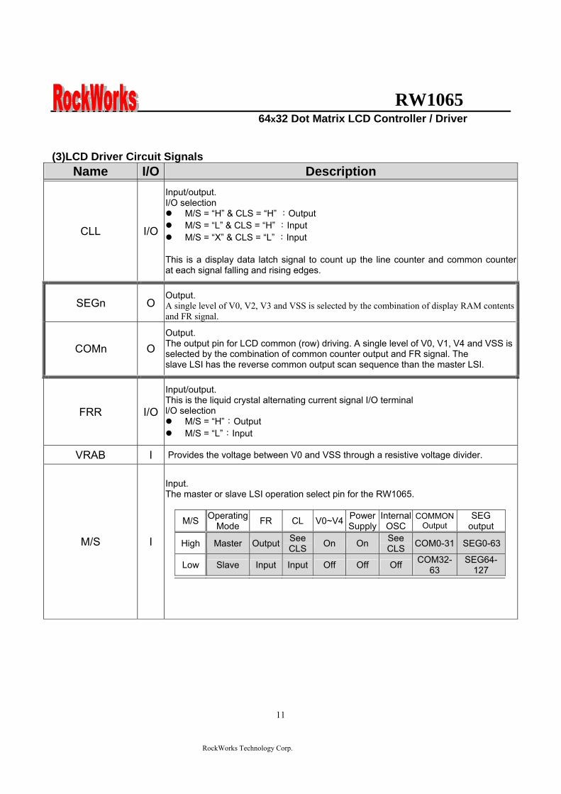
RW1065 64x32 Dot Matrix LCD Controller Driver
RockWorks Technology Corp
11
(3)LCD Driver Circuit Signals
Name IO Description
CLL IO
Inputoutput IO selection
MS = ldquoHrdquo amp CLS = ldquoHrdquo Output MS = ldquoLrdquo amp CLS = ldquoHrdquo Input MS = ldquoXrdquo amp CLS = ldquoLrdquo Input
This is a display data latch signal to count up the line counter and common counterat each signal falling and rising edges
SEGn O Output A single level of V0 V2 V3 and VSS is selected by the combination of display RAM contents and FR signal
COMn O Output The output pin for LCD common (row) driving A single level of V0 V1 V4 and VSS is selected by the combination of common counter output and FR signal The slave LSI has the reverse common output scan sequence than the master LSI
FRR IO
Inputoutput This is the liquid crystal alternating current signal IO terminal lO selection
MS = ldquoHrdquoOutput MS = ldquoLrdquoInput
VRAB I Provides the voltage between V0 and VSS through a resistive voltage divider
MS I
Input The master or slave LSI operation select pin for the RW1065
MS OperatingMode FR CL V0~V4 Power
SupplyInternal
OSC COMMON
Output SEG
output
High Master Output See CLS On On See
CLS COM0-31 SEG0-63
Low Slave Input Input Off Off Off COM32-63
SEG64-127
RW1065 64x32 Dot Matrix LCD Controller Driver
RockWorks Technology Corp
12
DESCRIPTION OF FUNCTIONS
The Parallel Interface (6800 series MPU)
Shared 6800 Series
RS RW Function
1 1 Reads the display data
1 0 Writes the display data
0 1 Status read
0 0 Write control data (command)
The Chip Select The RW1065 Series chips have two chip select terminals CS1
―BP and CS2P
When the chip select is inactive D0 to D7 enter a high impedance state and the RS E and RW inputs are inactive
The Accessing the Display Data RAM and the Internal Registers Data transfer at a higher speed is ensured since the MPU is required to satisfy the cycle time (tCYC) requirement alone in accessing the RW1065 Series Wait time may not be considered And in the RW1065 Series chips each time data is sent from the MPU a type of pipeline process between LSIs is performed through the bus holder attached to the internal data bus Internal data bus For example when the MPU writes data to the display data RAM once the data is stored in the bus holder then it is written to the display data RAM before the next data write cycle Moreover when the MPU reads the display data RAM
the first data read cycle (dummy) stores the read data in the bus holder and then the data is read from the bus holder to the system bus at the next data read cycle There is a certain restriction in the read sequence of the display data RAM Please be advised that data of the specified address is not generated by the read instruction issued immediately after the address setup This data is generated in data read of the second time Thus a dummy read is required whenever the address setup or write cycle operation is conducted This relationship is shown in Figure 2
RW1065 64x32 Dot Matrix LCD Controller Driver
RockWorks Technology Corp
13
E
Fig 2b read timing
E
RW
Fig 2a write timing (RW=rdquoLrdquo)
RS
RS
RW1065 64x32 Dot Matrix LCD Controller Driver
RockWorks Technology Corp
14
Display Data RAM The display data RAM is a RAM that stores the dot data for the display It has a 64 (8 page x 8 bit) x 64 bit structure It is possible to access the desired bit by specifying the page address and the column addressBecause as is shown in Figure 3 the D7 to D0 display data from the MPU corresponds to the liquid crystal display common direction there are few constraints at the time of display data transfer when multiple RW1065 series chips are used
thus and display structures can be created easily and with a high degree of freedom Moreover reading from and writing to the display RAM from the MPU side is performed through the IO buffer which is an independent operation from signal reading for the liquid crystal driver Consequently even if the display data RAM is accessed asynchronously during liquid crystal display it will not cause adverse effects on the display (such as flickering)
0
1
0
0
1
1
0
0
1
0
1
0
0
1
0
1
0
0
1
0
0
0
0
0
0
D0
D1
D2
D3
D4
-
Display data RAM Liquid crystal display
COM0
COM1
COM2
COM3
COM4
-
Figure3
The Page Address Circuit As shown in Figure 4 page address of the display data RAM is specified through the Page Address Set Command The page address must be specified again when changing pages to perform access
The Column Address As is shown in Table 4 the display data RAM column address is specified by the Column Address Set command The specified column address is incremented (+1) with each display data readwrite command This allows the MPU display data to be accessed continuously Moreover the increment of column addresses stops with 3FH Because the column address is independent of the page address when moving for example from page 0 column 3FH to page 1
column 00H it is necessary to respecify both the page address and the column address Furthermore as is shown in Table 4 the ADC command (segment driver direction select command) can be used to reverse the relationship between the display data RAM column address and the segment output Because of this the constraints on the IC layout when the LCD module is assembled can be minimized
Table 4 SEG Output
ADC set SEG0 SEG 63
ADC(D0)=0 0 rarr Column Address rarr 63 ADC(D0)=1 63 larr Column Address larr 0
RW1065 64x32 Dot Matrix LCD Controller Driver
RockWorks Technology Corp
15
Figure 4
Page Address D3 D2 D1 D0
DataSE
G0
SEG
1
SEG
2
SEG
3
SEG
4
SEG
5
SEG
6
SEG
7
SEG
8
helliphelliphelliphellip
SEG
55
SEG
56
SEG
57
SEG
58
SEG
59
SEG
60
SEG
61
SEG
62
SEG
63 SEG
COM
D0 COM0
D1 COM1
D2 COM2
D3 COM3
D4 COM4
D5 COM5
D6 COM6
0 0 0 0
D7
Page 0
COM7
D0 COM8
D1 COM9
D2 COM10
D3 COM11
D4 COM12
D5 COM13
D6 COM14
0 0 0 1
D7
Page 1
COM15
D0 COM16
D1 COM17
D2 COM18
D3 COM19
D4 COM20
D5 COM21
D6 COM22
0 0 1 0
D7
Page 2
COM23
D0 COM24
D1 COM25
D2 COM26
D3 COM27
D4 COM28
D5 COM29
D6 COM30
0 0 1 1
D7
Page 3
COM31
ADC=0 00
01
02
03
04
05
06
07
08
helliphelliphelliphellip 55
56
57
58
59
60
61
62
63
COLUMN ADC=1 63
62
61
60
59
58
57
56
55
helliphelliphelliphellip 08
07
06
05
04
03
02
01
00
RW1065 64x32 Dot Matrix LCD Controller Driver
RockWorks Technology Corp
16
Common Timing Generator Circuit Display Data Latch Circuit Generates common timing signals and FR frame signals from the CL basic clock The 132 or 164 duty (for RW1065) can be selected by the Duty Select command The 132 and 164 duties are provided by two chips consisting of the master and slave chips in the common multi-chip mode
This latch stores one line of display data for use by the LCD driver interface circuitry The output of this latch is controlled by the Display ONOFF
132 duty
164 duty
SHL=0
SHL=1
SHL=0
SHL=1
RW1065 64x32 Dot Matrix LCD Controller Driver
RockWorks Technology Corp
17
Display Timing Generator Circuit
The display timing generator circuit generates the timing signal to the line address circuit and the display data latch circuit using the display clock The display data is latched into the display data latch circuit synchronized with the display clock and is output to the data driver output terminal Reading to the display data liquid crystal driver circuits is completely independent of accesses to the display data RAM by the MPU Consequently even if the display data
RAM is accessed asynchronously during liquid crystal display there is absolutely no adverse effect (such asflickering) on the display Moreover the display timing generator circuit generates the common timing and the liquid crystal alternating current signal (FR) from the display clock It generates a drive wave form using a 2 frame alternating current drive method as is shown in Figure 5 for the liquid crystal drive circuit
Two-frame alternating current drive waveform
Figure 5
When multiple RW1065 Series chips are used the slave chip must be supplied the display timing signals(FR CL) from the master chip
Table 5 shows the status of the FR and CL signals
Table 5 Operating Mode FR CL
Master (MS = ldquoHrdquo) The internal oscillator circuit is enabled (CLS = ldquoHrdquo) The internal oscillator circuit is disabled (CLS = ldquoLrdquo)
Output Output
Output Input
Slave (MS = ldquoLrdquo) The internal oscillator circuit is enabled (CLS = ldquoHrdquo) The internal oscillator circuit is disabled (CLS = ldquoLrdquo)
Input Input
Input Input
RW1065 64x32 Dot Matrix LCD Controller Driver
RockWorks Technology Corp
18
The Liquid Crystal Driver Circuits
These are a 64-channel (RW1065) that generate four voltage levels for driving the liquid crystal The combination of the display data the COM scan signal and the FR signal
produces the liquid crystal drive voltage output Figure 6 shows examples of the SEG and COM output waveform
Figure 6
RW1065 64x32 Dot Matrix LCD Controller Driver
RockWorks Technology Corp
19
The Power Supply Circuit
The power supply circuits are low-power consumption power supply circuits that generate the voltage levels required for the liquid crystal drivers They comprise Booster circuits and voltage follower circuits They are only enabled in master operation The power supply circuits can turn on automatically after power on
Consequently it is possible to make an external power supply and the internal power supply function somewhat in parallel
The Liquid Crystal Voltage Generator Circuit The V0 voltage is produced by a resistive voltage divider outside the IC through VRAB pin and can be produced at the V1 V2 V3 and V4 voltage levels required for liquid crystal driving Moreover when the voltage follower changes the impedance it provides V1 V2 V3 and V4 to the liquid crystal drive circuit 15 bias or 16 bias or 18 bias or 19 bias for RW1065 can be selected by BS0 and BS1 pins V0-Vss maximum voltage is 15V Vout-Vss maximum voltage is 17V If VDD lt 35V it can use the Booster circuit 2x3x4xThe booster voltage can follow the spec condition (Vout-Vss ≦ 17V max voltage) if VDD gt35V only use the 2X3X booster circuit that can ensure the V0-Vss voltage ≦ 15V If use the VDD voltage 5V and 4X booster itrsquos over the spec operation condition To turn on built-in power (boosterfollower) must waiting 200mS to display on for boosterfollower stable Therefore power off must follower ldquopower off sequencerdquo too
Power on Display off
Power off
Power off sequence
Wait time gt200mS
Display on
Power on sequence
RW1065 64x32 Dot Matrix LCD Controller Driver
RockWorks Technology Corp
20
The Reset Circuit
When the RTP input comes to the ldquoLrdquo level these LSIs return to the default state Their default states are as follows 1 Display OFF 2 Display all point on is select to normal 3 Display normalreverse is select to normal 4 164 duty is selected 5 Read modify write OFF 6 Column address set to Address 0 7 Page address set to Page 0 8 Start line set to first line 9 Frame frequency set to default 10 Power save mode released 11 Ext set to ldquo0rdquo When the power is turned on the IC internal state becomes unstable and it is necessary to initialize it using the RSTP terminal After the initialization each input terminal should be controlled normally While RSTP is ldquoLrdquo the oscillator works but the display timing generator stops and the CL FR terminals are fixed to ldquoHrdquo The terminals D0 to D7 are not affected
RW1065 64x32 Dot Matrix LCD Controller Driver
RockWorks Technology Corp
21
TABLE OF RW1065 INSTRUCTIONS
Instruction code Instruction RS RW DB7 DB6 DB5 DB4 DB3 DB2 DB1 DB0 Description
EXT=0 or 1
MODE SET 0 0 0 0 0 0 1 1 0 EXT Set EXT mode
Instruction code Instruction RS RW DB7 DB6 DB5 DB4 DB3 DB2 DB1 DB0 Description
EXT=0 Display ONOFF 0 0 0 0 1 1 1 1 1 D D=0Display OFF
D=1Display ONSet page address 0 0 1 0 1 1 1 P2 P1 P0 Set page address
Set column address 0 0 0 1 Y5 Y4 Y3 Y2 Y1 Y0 Set column
address MSB
Read Status 0 1 BUSY 0 ON OFF RESET 0 0 0 0 Read register
status Write display
data 1 0 Write data Write data into DDRAM
Read display data 1 1 Read data Read data from
DDRAM Set initial
display line register
0 0 1 1 S5 S4 S3 S2 S1 S0 Specify the initial
display line to realize vertical scrolling
Instruction code Instruction RS RW DB7 DB6 DB5 DB4 DB3 DB2 DB1 DB0 Description
EXT=1
NOP 0 0 0 0 0 0 0 0 0 0 no operation
Set modiy-read 0 0 0 0 0 0 1 0 0 0 Set modiy-read
mode
END 0 0 0 0 0 0 1 1 1 0 release modiy-read mode
Set power save mode 0 0 0 0 0 0 0 0 1 PSAVE P=0 normal mode
P=1 sleep mode
0 0 0 0 0 1 0 1 Display
COMMAND (double
command)
0 0 FRSEL
0 0 0 0 REV ALLON DUTY
DUTY=1 64 duty DUTY=0 32 duty ALLON=1display all on ALLON=0display
normal REV=1display reverse REV=0display normal FRSEL=1FR frequency double default FRSEL=0FR frequency default
RW1065 64x32 Dot Matrix LCD Controller Driver
RockWorks Technology Corp
22
Command Description
See the Table of RW1065 instructions The RW1065 series identifies a data bus using a combination of RS E and RW signals As the MPU translates a command in the internal timing only (independent from the external clock) its speed is very high The busy check is usually not required
Display ONOFF
EXT RS RW D7 D6 D5 D4 D3 D2 D1 D0
0 0 0 0 0 1 1 1 1 1 D
This command turns the display on and off D=1 Display ON D=0 Display OFF(default)
Set page Address This command specifies the page address that corresponds to the low address of the display data RAM when it is accessed by the MPU Any bit of the display data RAM can be accessed when its page address and column address are specified The display status is not changed even when the page address is changed
EXT RS RW D7 D6 D5 D4 D3 D2 D1 D0
0 0 0 1 0 1 1 1 A2 A1 A0
This command loads the page address register
A2 A1 A0 Page
0 0 0 0 (default)
0 0 1 1 0 1 0 2 0 1 1 3 1 0 0 4 1 0 1 5 1 1 0 6 1 1 1 7
Page mapping see Figure 4
RW1065 64x32 Dot Matrix LCD Controller Driver
RockWorks Technology Corp
23
Set Column Address This command specifies a column address of the display data RAM When the display data RAM is accessed by the MPU continuously the column address is incremented by I each time it is accessed from the set address Therefore the MPU can access to data continuously The column address stops to be incremented at address 63 and the page address is not changed continuously
EXT RS RW D7 D6 D5 D4 D3 D2 D1 D0
0 0 0 0 1 A5 A4 A3 A2 A1 A0
A5 A4 A3 A2 A1 A0 Column Address0 0 0 0 0 0 0(default) 0 0 0 0 0 1 1
1 1 1 1 1 1 63
Read Status
EXT RS RW D7 D6 D5 D4 D3 D2 D1 D0
0 0 1 BUSY 0 ON OFF RESET 0 0 0 0
The BUSY Flag bit indicates that RW 1065 is operating or no operating
BUSY=1 Operation BUSY=0 Ready
The ONOFF bit indicates the current status of the display It is the inverse of the polarity of the display ONOFF command ONOFF=1 Display OFF ONOFF=0 Display ON The RESET bit indicates whether the driver is executing a hardware or software reset or if it is in normal operating mode RESET=1 Currently executing reset command RESET=0 Normal operation
RW1065 64x32 Dot Matrix LCD Controller Driver
RockWorks Technology Corp
24
Write Display Data
EXT RS RW D7 D6 D5 D4 D3 D2 D1 D0
0 1 0 Write data
Writes 8-bits of data into the display data RAM at a location specified by the contents of the column address and page address registers and then increments the column address register by one
Read Display Data
EXT RS RW D7 D6 D5 D4 D3 D2 D1 D0
0 1 1 Read data
Reads 8-bits of data from the data IO latch updates the contents of the IO latch with display data from the display data RAM location specified by the contents of the column address and page address registers and then increments the column address register After loading a new address into the column address register one dummy read is required before valid data is obtained
Set initial display line register
EXT RS RW D7 D6 D5 D4 D3 D2 D1 D0
0 0 0 1 1 S5 S4 S3 S2 S1 S0
Loads the RAM line address of the initial display line COM 0 into the initial display line register The RAM display data becomes the top line of the LCD screen It is followed by the higher number lines in ascending order corresponding to the duty cycle The screen can be scrolled using this command by incrementing the line address(default value=rdquo00Hrdquo)
RW1065 64x32 Dot Matrix LCD Controller Driver
RockWorks Technology Corp
25
Read-Modify-Write
EXT RS RW D7 D6 D5 D4 D3 D2 D1 D0
1 0 0 0 0 0 0 1 0 0 0
This command defeats column address register auto-increment after data reads The current contents of the column Address register are saved The mode remains active until an End command is received When the End command is entered the column address is returned to the one used during input of Read-Modify-Write Command This function can reduce the load of MPU when data change is repeated as a specific display area Any command other than Data Read or Write can be used in the Read-Modify-Write mode However the Column Address Set command cannot be used
End
EXT RS RW D7 D6 D5 D4 D3 D2 D1 D0
1 0 0 0 0 0 0 1 1 1 0
This command cancels read-modify-write mode and restores the contents of the column address register to their value prior to the receipt of the Read-Modify-Write command
N N+1 N+2 N+3 N+m N
Read -modify-write mode set End
Returm
Column address
Set page address
Set column address
Read-modify-write
Dummy read
Read data
Write data
End
CompletedNo
Yes
RW1065 64x32 Dot Matrix LCD Controller Driver
RockWorks Technology Corp
26
Set power save mode
EXT RS RW D7 D6 D5 D4 D3 D2 D1 D0
1 0 0 0 0 0 0 0 0 1 PSAVE
When power save mode is entered thus greatly reducing power consumption In the power save mode the display data is saved as is the operating mode that was in effect before the power saver mode was initiated and the MPU is still able to access the display data RAM PSAVE=1 Sleep mode PSAVE=0 Normal mode Sleep mode This stops all operations in the LCD display system and as long as there are no accesses from the MPU the consumption current is reduced to a value near the static current The internal modes during sleep mode are as follows 1 The oscillator circuit and the LCD power supply circuit are halted 2 All liquid crystal drive circuits are halted and the segment and common drive outputs output a Vss level
Display command double command
EXT RS RW D7 D6 D5 D4 D3 D2 D1 D0
1 0 0 0 0 0 0 0 1 0 1
1 0 0 FRSEL 0 0 0 0 REV ALLON DUTY
Display NormalReverse set REV=1 Reverse REV=0 Normal(default) Display All Point ONOFF ALLON=1 All display points ON ALLON=0 Normal(default) Select Duty Duty=1 164 duty cycle(default) Duty=0 132 duty cycle FRAME FREQUENCY Select FRSEL=1 Double FRSEL=0 (default)
RW1065 64x32 Dot Matrix LCD Controller Driver
RockWorks Technology Corp
27
Hardware Pin Set
Select ADC by ADC Pin The pin selects the relationship between display data RAM column addresses and segment drivers ADC=1 SEG0larrcolumn address 3FHhellipinverted ADC=0 SEG0larrcolumn address 00Hhellipnormal(default) This command is provided to reduce restrictions on the placement of driver ICs and routing of traces during printed circuit Board design See Figure 4 for a table of segments and column addresses for the two values of D
Select SHL by SHL Pin The pin selects the com output scan direction SHL=1 Reverse directioncom63rarrcom0 SHL=0 Normal com0rarrcom63 Both master and slave should set identical SHL value
Select LCD Bias by BS0 BS1 Pin
BS1 BS0 Bias 0 0 15 bias 0 1 16 bias 1 0 18 bias 1 1 19 bias
RW1065 64x32 Dot Matrix LCD Controller Driver
RockWorks Technology Corp
28
When an External Resistance is Used The liquid crystal power supply voltage V0 is set by adding resistors Rarsquo and Rbrsquo between VDD and VR and between VR and V0 respectively
RW1065
RW1065 64x32 Dot Matrix LCD Controller Driver
RockWorks Technology Corp
29
The set voltage circuits
Using the step-up voltage circuits equipped within the RW1065 chips it is possible to produce a 2X 3X 4X step-up voltage levels 2X step-up
To produce voltage level in the positive direction at the Vout terminal that is 2 times the voltage difference between VSS and VDD2 Please configure set voltage circuits like this Place a 1uF~22uF capacitor between CAP1N and CAP1P Place a 1uF~22uF capacitor between VSS and VOUT Short CAP2P CAP3P and VOUT Leave CAP2N open 3X step-up
To produce voltage level in the positive direction at the Vout terminal that is 3 times the voltage difference between VSS and VDD2 Please configure set voltage circuits like this Place a 1uF~22uF capacitor between CAP1N and CAP1P Place a 1uF~22uF capacitor between VSS and VOUT Place a 1uF~22uF capacitor and 100 ohms resistor between CAP2N and CAP2P Short CAP3P and Vout 4X step-up
To produce voltage level in the positive direction at the Vout terminal that is 4 times the voltage difference between VSS and VDD2 Please configure set voltage circuits like this Place a 1uF~22uF capacitor between CAP1N and CAP1P Place a 1uF~22uF capacitor between VSS and VOUT Place a 1uF~22uF capacitor and 100 ohms resistor between CAP2N and CAP2P Place a 1uF~22uF capacitor and 100 ohms resistor between CAP1N and CAP3P
RW1065 64x32 Dot Matrix LCD Controller Driver
RockWorks Technology Corp
30
ABSOLUTE MAXIMUM RATINGS Characteristics Symbol Value Unit
Power supply voltage VDD -03 to +70 V
LCD driver voltage Vout 0 to +17 V
Input voltage VIN -03 to VDD+03 V
Operating temperature TA -40 to +85
Storage temperature TSTO -55 to +125
DC CHARACTERISTICS
Rating Item Symbol Condition Min Typ Max Unit ApplicablePin
Operating Voltage VDD - 27 30 55 V VDD1
Step up output voltage Vout (Relative to VDD) 0 - 17 V Vout
Voltage follower circuit operating Voltage V0 (Relative to VDD) 0 - 15 V V0
V0 accuracy V0 - 0 - 15 V0
High-level Input Voltage Low-level Input Voltage
VIHC VILC - 07 VDD
Vss - VDD 09 V 2
High-level Output Voltage Low-level Output Voltage
VOHC VOLC
IOH = ndash05 mA IOL = 05 mA
08VDD Vss - VDD
02 VDD V 3
Input leakage current ILI VIN = VDD or VSS -1 - 2 uA 4
Output leakage current ILO - -1 1 uA 5
Liquid Crystal Driver ON Resistance RON
Ta= 25degC(Relative To VDD)
V0 =15 V - 16 20 KΩ SEGn COMn 6
Internal Oscillator fOSC 2286 254 2794 Oscillator
Frequency External Input RECOMMAND fCL
Ta = 25degC 132Duty 2286 254 2794
kHz CL
Internal Oscillator fOSC 45 5 55 Oscillator
Frequency External Input RECOMMAND fCL
Ta = 25degC 164Duty 45 5 55
kHz CL
bullDynamic Consumption Current During Display with the Internal Power Supply OFF Current consumed by total ICs when an external power supply is used
Unless otherwise specified Vss=0V VDD=30V
RW1065 64x32 Dot Matrix LCD Controller Driver
RockWorks Technology Corp
31
Display Pattern OFF
Ta = 25degC Vout=17V Rating Item Symbol Condition Min Typ Max Unit Notes
VDD=30 V V0-Vss=8V - 10 15 RW1065 IDD VDD=50 V V0-Vss=8V - 35 45
microA 7
Display Pattern Checker
Ta = 25degC Vout=17V Rating Item Symbol Condition Min Typ Max Unit Notes
VDD=30 V V0-Vss=8V - 15 20 RW1065 IDD VDD=50 V V0-Vss=8V - 40 50
microA 7
Display Pattern OFF
Ta = 25degC Vout=17V Rating Item Symbol Condition Min Typ Max Unit Notes
VDD=30 V V0-Vss=8V - 15 20 RW1065 IDD VDD=50 V V0-Vss=8V - 40 50
microA 7
Display pattern Checker
Ta = 25degC Vout=17V Rating Item Symbol Condition Min Typ Max Unit Notes
VDD=30 V V0-Vss=8V - 65 80 RW1065 IDD VDD=50 V V0-Vss=8V - 130 150
microA 7
bull Consumption Current at Time of Power Saver Mode VSS = 0 V VDD = 30 V plusmn 10
Rating Item Symbol Condition Min Typ Max Unit Notes
Sleep mode IDD - - 5 10 microA -
References for items market with 1 While a broad range of operating voltages is guaranteed performance cannot be guaranteed if there are sudden fluctuations to the
voltage while the MPU is being accessed 2 The RS D0 to D5 D6 D7 E RW CS1BP CS2P CLS CL FR MS and RST
― terminals
3 The D0 to D7 FR and CL terminals 4 The RS E RW CS1BP CS2P CLS MS and RST
― terminals
5 Applies when the D0 to D5 D6 D7 CL and FR terminals are in a high impedance state 6 These are the resistance values for when a 01 V voltage is applied between the output terminals SEGn or COMn and
the various power supply terminals (V1 V2 V3 and V4) These are specified for the operating voltage (3) range RON = 01 V ∆I (Where ∆I is the current that flows when 01 V is applied while the power supply is ON)
7 It indicates the current consumed on ICs alone when the internal oscillator circuit and display are turned on Does not include the current due to the LCD panel capacity and wiring capacity Applicable only when there is no access from the MPU
RW1065 64x32 Dot Matrix LCD Controller Driver
RockWorks Technology Corp
32
TIMING CHARACTERISTICS
68 Interface
(Ta=-40 to 85 degC) VDD=27 to 45V
Rating VDD=45 to 55V
Rating Item Signal Symbol ConditionMin Max Min Max
Units
Address hold time RS tAH6 0 mdash 0 mdash Address setup time RS tAW6
mdash 0 mdash 0 mdash
ns
System cycle time RS tCYC6 mdash 900 mdash 800 mdash ns Data setup time D0 to D7 tDS6 100 mdash 100 mdash Data hold time D0 to D7 tDH6
mdash 0 mdash 0 mdash
ns
Access time D0 to D7 tACC6 mdash 350 mdash 250
Output disable time D0 to D7 tOH6 CL = 100 pF
mdash 300 mdash 200 ns
Read tEWHR 360 mdash 300 mdash Enable H pulse time
WriteE
tEWHW mdash
360 mdash 300 mdash ns
Read tEWLR 450 mdash 400 mdash Enable L pulse time
WriteE
tEWLW mdash
450 mdash 400 mdash ns
1 All timing is specified using 20 and 80 of VDD as the reference 2 tEWLW and tEWLR are specified as the overlap between CS1BP being ldquoLrdquo (CS2P = ldquoHrdquo) and E
RW1065 64x32 Dot Matrix LCD Controller Driver
RockWorks Technology Corp
33
Reset Timing
Rating Item Signal Symbol Condition
Min Typ Max Units
Reset time mdash tR mdash mdash - 2 micros
Reset ldquoLrdquo pulse width RST tRW mdash 2 - mdash micros
1 When double chip was be used then the duty set command must be set between the tR
RW1065 64x32 Dot Matrix LCD Controller Driver
RockWorks Technology Corp
34
IO PAD CONFIGURATION
RW1065 64x32 Dot Matrix LCD Controller Driver
RockWorks Technology Corp
35
THE MPU INTERFACE (REFERENCE EXAMPLES) The RW1065 Series can be connected to 6800 Series MPUs The display area can be enlarged by using multiple RW1065 Series chips When this is done the chip select signal can be used to select the individual ICs to access
6800 Series MPUs
RW
106
5
RW1065 64x32 Dot Matrix LCD Controller Driver
RockWorks Technology Corp
36
When using external multi-level power supply for LCD driving (REFERENCE EXAMPLE)
Using a resistor divider can provide RW1065 external multi-level power supply for LCD driving
The circuit below shows a resistor divider network which can bias V0 V1 V2 V3 and V4 externally
RW1065 64x32 Dot Matrix LCD Controller Driver
RockWorks Technology Corp
37
bullWhen V0 V1 V2 V3 and V4 are biased by external power supply analog section of RW1065 should be turn off by software during LCD initialization The example in below shows the sequence to turn off analog section when external bias is used Begin of LCD initialization 1 Reset RW1065 2 SET EXT=1 (mode instruction)
RS RW DB7 DB6 DB5 DB4 DB3 DB2 DB1 DB00 0 0 0 0 0 1 1 0 1
3 SET Display Command (double command)
RS RW DB7 DB6 DB5 DB4 DB3 DB2 DB1 DB00 0 0 0 0 0 0 1 0 1 0 0 0 0 1 1 0 0 0 1
4 SET EXT=1 (mode instruction)
RS RW DB7 DB6 DB5 DB4 DB3 DB2 DB1 DB00 0 0 0 0 0 1 1 0 0
End of LCD initialization
bullBecause pins can not set LCD bias when external power supplies are used for LCD driving the bias can be set by an appropriate configuration for a resistor voltage divider networks The example is shown below
VSS
R
R
NR
R
R
RV1
RV2
RV3
RV4
V0
Bias Network Circuit Concept 15 Bias N=1 total = 5R 16 Bias N=2 total =6R 18 Bias N=4 total =8R 19 Bias N=5 total = 9R
RW1065 64x32 Dot Matrix LCD Controller Driver
RockWorks Technology Corp
38
Single chip solution for RW1065 application (REFERENCE EXAMPLE)
For a 64x32 application the duty cycle of LCD panel is 164 and the display duty of RW1065 should be set to 164 The display duty cycle can be selected by the DUTY bit in display command The diagram for 64x32 application is shown below
64 SEGx32COM LCD Panel
164 duty cycle
RW1065 DUTY=1
COM1~33
SEG1~65
RW1065 64x32 Dot Matrix LCD Controller Driver
RockWorks Technology Corp
39
Using an adjustable resistor on the main board to adjust the contrast of liquid crystal display (REFERENCE EXAMPLE)
The schematic shows an adjustable resistor on main board that can adjust voltage level of V0
RW1065 64x32 Dot Matrix LCD Controller Driver
RockWorks Technology Corp
40
Package information (Please pay close attention to the information in this section Do not hesitate to consult with our sale representative if you have any question or concern)
In order to make better bonding yield for RW1065 please follow the tips and recommendations in this section In this section few tips about COB footprint style PCB layout and wire bonding will be discussed
The drawing in below shows the PCB footprint style which we recommend for RW1065 Pads array in
curve shape is easier for Al wire bonding Besides that a real size COB footprint for RW1065 is also shown in below RW1065 COB footprint is also available in powerpcb or protel format for design reference purpose
The ratio is 11
RW1065 64x32 Dot Matrix LCD Controller Driver
RockWorks Technology Corp
41
During COB footprint design there have some tips about footprint that the PCB designer should know The angle between bonding wire and vertical line should less than 45 Otherwise the wire shorts would become very easy to happen at fours corners of the chip
The angle between bonding wire and vertical line could be reduced by expanding the distance between pads array and the chip In addition reducing length in horizon direction of pads array could minimize the angle between bonding wire and vertical line The picture in below will help to illustrate this concept From the experiences COB footprint style affects the bonding yield
Bad Wires are too close to each other
The angle between bonding wire and vertical line is greater than 45
The angle between bonding wire and vertical line is less than 45
Wires are not too close to each other
Reducing length in horizon direction of pads array could minimize the angle between bonding wire and vertical line
The angle between bonding wire and vertical line could be reduced by expanding the distance between pads array and the chip
RW1065 64x32 Dot Matrix LCD Controller Driver
RockWorks Technology Corp
42
If the gap between pads of COB footprint is filled with solder mask coating it is difficult to bond Al wire to
the pads The top solder masks layer that overlap COB footprint area should be removed
Please use 1 mils diameter Al wire for RW1065 wire bonding
1 2 3 4 5 6
A
B
C
D
654321
D
C
B
A
Title
Number RevisionSize
C
Date 29-Aug-2007 Sheet of File D公司資料99seMyDesignddb Drawn By
RW1065
COM131
COM142
COM153
COM164
COM175
COM186
COM197
COM208
COM219
COM2210
COM2311
COM2412
COM2513
COM2614
COM2715
COM2816
COM2917
COM3018
COM3119
SEG
6320
SEG
6221
SEG
6122
SEG
6023
SEG
5924
SEG
5825
SEG
5726
SEG
5627
SEG
5528
SEG
5429
SEG
5330
SEG
5231
SEG
5132
SEG
5033
SEG
4934
SEG
4835
SEG
4736
SEG
4637
SEG
4538
SEG
4439
SEG
4340
SEG
4241
SEG
4142
SEG
4043
SEG
3944
SEG
3845
SEG
3746
SEG
3647
SEG
3548
SEG
3449
SEG
3350
SEG
3251
SEG
3152
SEG
3053
SEG
2954
SEG
2855
SEG
2756
SEG
2657
SEG
2558
SEG
2459
SEG
2360
SEG
2261
SEG
2162
SEG
2063
SEG
1964
SEG
1865
SEG
1766
SEG
1667
SEG
1568
SEG
1469
SEG13 70SEG12 71SEG11 72SEG10 73SEG9 74SEG8 75SEG7 76SEG6 77SEG5 78SEG4 79SEG3 80SEG2 81SEG1 82SEG0 83ADCP 84CLL 85
VSS
86D
087
D1
88D
289
D3
90D
491
D5
92D
693
D7
94C
S1B
P95
CS2
P96
ERD
P97
AO
P(R
S)98
RW
RP
99V
DD
100
RST
P10
1C
LSP
102
FRR
103
MSP
104
BS1
P10
5B
S0P
106
SHLP
107
VD
D2
108
CA
P2N
109
CA
P2P
110
CA
P1P
111
CA
P1N
112
CA
P3P
113
VO
UT
114
V0
115
VR
AB
116
V3
117
V2
118
V4
119
V1
120
CO
M0
121
CO
M1
122
CO
M2
123
CO
M3
124
CO
M4
125
CO
M5
126
CO
M6
127
CO
M7
128
CO
M8
129
CO
M9
130
CO
M10
131
CO
M11
132
CO
M12
133
4897x1902 um
IC1
RW1065
C9CAPR4
100R0603
R30R0603
C8
CAP
C7
CAP
R2
100R0603
R1
0R0603C6 22uf
R50R
R6300R
R7RES1
R8NC R9
100R0603
VDD
R10
NC
R11
100R0603
R12
100R0603
R13
NC
R14
100R0603
R15
NC
VDD
D0
D1
D2
D3
D4
D5
D6
D7
DB[07]
VDDC5
01uf0603
VD
D
CS2
P
123456789
1011121314151617181920
J1
CON20
C1201uf0603
R3951K0603
VDD
CAP Value1UF~22UF
2XPut C6C8 Short R1R3Open R2R4C7C93XPut C6C8C9 R4Short R1Open R2R3C74XOpen R1R3
BS0 BS1 Bias0 0
0 1
1 0
11
15 bias
16 bias
18 bias
19 bias
ADC=0 SEG0lt~column address 00Hnormal(default) ADC=1 SEG0lt~column address 3FHinverted
SHL=0 Normal COM0~gtCOM63(default)SHL=1 Reverse direction COM63~gtCOM0
R16100R0603
LCD PANEL 64X32RockWorks
RW1065 64X32
COM0-31 SEG0-63SHL=0 ADC=0
SHL=1COM31-0
ADC=1SEG63-0
if use single chip for 32 command displaythe display command must select 164 dutyDisplay panel must select 164 duty type
VO
UT
C3P
C1N
C1P
C2P
C2N
VDD2
ADC
SHL
BS0
BS1
CLLADC
V1
V2
V3
V4
VR
AB
V0
VO
UT
C3P
C1N
C1P
C2P
C2N
VD
D2
SHL
BS0
BS1
FRR
RST
P
RW
RS
E CS1
B
CS1
V0RSRWED0D1D2D3D4D5D6D7
RSTPAK
C4
22uf
RBRES1
RA1RES1
C2
22uf
C1
22uf
C3
22uf
C0
22uf
R20
100k0603
R21
100k0603
R17
200K0603
V1
V2
V3
V4 VRAB
V0
V0
OPTION
B
R18
300R0603
RA2RES1
VADJ
R19100R
R23 RES1R22 0R
R24
RES1
R25
0R
VDD
CS1BP
CS2P
CS1
CS1
R26
22R0603
R27
22R0603
C1047uf
C11
01uf
VSS_INVDD_IN
D1DIODE
FGND
鐵框地
VSS
VDD
R28 10RR29 10RR30 10RR31 10RR32 10RR33 10RR34 10RR35 10RR36 10RR37 10RR38 10R
VADJ
1 2 3 4 5 6
A
B
C
D
654321
D
C
B
A
Title
Number RevisionSize
C
Date 29-Aug-2007 Sheet of File D公司資料99seMyDesignddb Drawn By
RW1065
COM131
COM142
COM153
COM164
COM175
COM186
COM197
COM208
COM219
COM2210
COM2311
COM2412
COM2513
COM2614
COM2715
COM2816
COM2917
COM3018
COM3119
SEG
6320
SEG
6221
SEG
6122
SEG
6023
SEG
5924
SEG
5825
SEG
5726
SEG
5627
SEG
5528
SEG
5429
SEG
5330
SEG
5231
SEG
5132
SEG
5033
SEG
4934
SEG
4835
SEG
4736
SEG
4637
SEG
4538
SEG
4439
SEG
4340
SEG
4241
SEG
4142
SEG
4043
SEG
3944
SEG
3845
SEG
3746
SEG
3647
SEG
3548
SEG
3449
SEG
3350
SEG
3251
SEG
3152
SEG
3053
SEG
2954
SEG
2855
SEG
2756
SEG
2657
SEG
2558
SEG
2459
SEG
2360
SEG
2261
SEG
2162
SEG
2063
SEG
1964
SEG
1865
SEG
1766
SEG
1667
SEG
1568
SEG
1469
SEG13 70SEG12 71SEG11 72SEG10 73SEG9 74SEG8 75SEG7 76SEG6 77SEG5 78SEG4 79SEG3 80SEG2 81SEG1 82SEG0 83ADCP 84CLL 85
VSS
86D
087
D1
88D
289
D3
90D
491
D5
92D
693
D7
94C
S1B
P95
CS2
P96
ERD
P97
AO
P(R
S)98
RW
RP
99V
DD
100
RST
P10
1C
LSP
102
FRR
103
MSP
104
BS1
P10
5B
S0P
106
SHLP
107
VD
D2
108
CA
P2N
109
CA
P2P
110
CA
P1P
111
CA
P1N
112
CA
P3P
113
VO
UT
114
V0
115
VR
AB
116
V3
117
V2
118
V4
119
V1
120
CO
M0
121
CO
M1
122
CO
M2
123
CO
M3
124
CO
M4
125
CO
M5
126
CO
M6
127
CO
M7
128
CO
M8
129
CO
M9
130
CO
M10
131
CO
M11
132
CO
M12
133
4897x1902 um
IC1
RW1065 Master
RW1065
COM131
COM142
COM153
COM164
COM175
COM186
COM197
COM208
COM219
COM2210
COM2311
COM2412
COM2513
COM2614
COM2715
COM2816
COM2917
COM3018
COM3119
SEG
6320
SEG
6221
SEG
6122
SEG
6023
SEG
5924
SEG
5825
SEG
5726
SEG
5627
SEG
5528
SEG
5429
SEG
5330
SEG
5231
SEG
5132
SEG
5033
SEG
4934
SEG
4835
SEG
4736
SEG
4637
SEG
4538
SEG
4439
SEG
4340
SEG
4241
SEG
4142
SEG
4043
SEG
3944
SEG
3845
SEG
3746
SEG
3647
SEG
3548
SEG
3449
SEG
3350
SEG
3251
SEG
3152
SEG
3053
SEG
2954
SEG
2855
SEG
2756
SEG
2657
SEG
2558
SEG
2459
SEG
2360
SEG
2261
SEG
2162
SEG
2063
SEG
1964
SEG
1865
SEG
1766
SEG
1667
SEG
1568
SEG
1469
SEG13 70SEG12 71SEG11 72SEG10 73SEG9 74SEG8 75SEG7 76SEG6 77SEG5 78SEG4 79SEG3 80SEG2 81SEG1 82SEG0 83ADCP 84CLL 85
VSS
86D
087
D1
88D
289
D3
90D
491
D5
92D
693
D7
94C
S1B
P95
CS2
P96
ERD
P97
AO
P(R
S)98
RW
RP
99V
DD
100
RST
P10
1C
LSP
102
FRR
103
MSP
104
BS1
P10
5B
S0P
106
SHLP
107
VD
D2
108
CA
P2N
109
CA
P2P
110
CA
P1P
111
CA
P1N
112
CA
P3P
113
VO
UT
114
V0
115
VR
AB
116
V3
117
V2
118
V4
119
V1
120
CO
M0
121
CO
M1
122
CO
M2
123
CO
M3
124
CO
M4
125
CO
M5
126
CO
M6
127
CO
M7
128
CO
M8
129
CO
M9
130
CO
M10
131
CO
M11
132
CO
M12
133
4897x1902 um
IC2
RW1065 Slave
C4
22uf
RBRES1
RA1RES1
C2
22uf
C1
22uf
C3
22uf
C0
22ufC9CAPR4
100R0603
R30R0603
C8
CAP
C7
CAP
R2
100R0603
R1
0R0603C6 22uf
R50R0603
R6300R0603
R7RES1
R8NC R9
100R0603
VDD
R10
NC
R11
100R0603
R12
NC
R13
100R0603
R14
100R0603
R15
NC
R16
100R0603
R17
NC
VDD
D0
D1
D2
D3
D4
D5
D6
D7
D0
D1
D2
D3
D4
D5
D6
D7
DB[07] DB[07]
VDDC10
01uf0603
VD
D
IC1_
CS2
P
VDD
IC2_
CS2
P
VD
D
C11
01uf0603
VSS
VSS
LCD PANEL 128X64
Master COM0-31 Slave COM32-63
Master SEG0-63 Slave SEG64-127
123456789
1011121314151617181920
J1
CON20
Master Slave
CAP Value1UF~22UF
2XPut C6C8 Short R1R3Open R2R4C7C93XPut C6C8C9 R4Short R1Open R2R3C74XOpen R1R3
RockWorksRW1065 128x64
BS0 BS1 Bias0 0
0 1
1 0
11
15 bias
16 bias
18 bias
19 bias
ADC=0 SEG0lt~column address 00Hnormal(default) ADC=1 SEG0lt~column address 3FHinverted
SHL=0 Normal COM0~gtCOM63(default)SHL=1 Reverse direction COM63~gtCOM0Both Master and Slave should set identical SHL value
SHL=0 SHL=0
ADC=0 ADC=0
Slave COM31-0
Slave SEG127-64
SHL=1
ADC=1
SHL=1Master COM63-32
ADC=1Master SEG63-0
R18100R0603
R22
100k0603
R23
100k0603
C501uF0603
R4551K0603
VDD
R19
200K0603
ADC1
ADC2
SHL
BS0
BS1
VDD2
V1
V2
V3
V4 VRAB
V0
V0V
OU
T
C3P
C1N
C1P
C2P
C2N
V1
V2
V3
V4
VR
AB
V0
VO
UT
C3P
C1N
C1P
C2P
C2N
VD
D2
SHL
BS0
BS1
FRR
RST
P
RW
RS
E IC1_
CS1
BP
V1
V2
V3
V4
VR
AB
V0
VO
UT
VD
D2
SHL
BS0
BS1
FRR
RST
P
RW
RS
E IC2_
CS1
BP
CLLADC1
CLLADC2
RSTP
CS1CS2
V0RSRWED0D1D2D3D4D5D6D7
AK
OPTION
R20
300R0603
RA2RES1
VADJ
R21
100R
B
R25 RESR24 0R
R26 RES R27 0RVDD
IC1_CS1BP
IC1_CS2P
CS1
CS1
R28 0R R29 RES
R30 RES R31 0R
IC2_CS1BP
IC2_CS2P
CS2
CS2
R32
22R0603
R33
22R0603
C1001uf
C11
47uf
D1DIODE
FGND
鐵框地
VSS
VDD
R34 10RR35 10RR36 10RR37 10RR38 10RR39 10RR40 10RR41 10RR42 10RR43 10RR44 10R
VSS_INVDD_IN
VADJ
VDD
1 2 3 4 5 6 7 8
A
B
C
D
87654321
D
C
B
A
Title
Number RevisionSize
D
Date 29-Aug-2007 Sheet of File D公司資料 99seMyDesignddb Drawn By
C422uf
RBRES1
RA1RES1
C3
22uf
C2
22uf
C1
22uf
C0
22ufC9CAPR4
100R0603
R30R0603
C8
CAP
C7
CAP
R2
100R0603
R1
0R0603C6 22uf
R220R0603
R23300R0603
R24RES1
R39
NCR40
100 ohm0603
VDD
R41
NC
R42
100 ohm0603
R43
NC
R44
100 ohm0603
R45
NC
R46
100 ohm0603
R47
100 ohm0603
R48
NC
R49
100 ohm0603
R50
NC
VDDCAP Value1UF~22UF
2XPut C6C8 Short R1R3Open R2R4C7C93XPut C6C8C9 R4Short R1Open R2R3C74XOpen R1R3
BS0 BS1 Bias0 0
0 1
1 0
11
15 bias
16 bias
18 bias
19 bias
ADC=0 SEG0lt~column address 00Hnormal(default)
ADC=1 SEG0lt~column address 3FHinverted
SHL=0 Normal COM0~gtCOM63(default)SHL=1 Reverse direction COM63~gtCOM0Both Master and Slave should set identical SHL value
R7
100k0603
R8
100k0603
V1
V2
V3
V4
V0
VRAB
V0
R5
200K
VDD2
VO
UT
C3P
C1N
C1P
C2P
C2N
ADC1
ADC2
ADC3
SHL
BS0
BS1
CS1CS2CS3
V0RSRWED0D1D2D3D4D5D6D7
RSTP
R3851K0603
C5
01uF
VDD
OPTION
R6
300R0603R9100R
RA2RES1
VADJ
RW1065
COM131
COM142
COM153
COM164
COM175
COM186
COM197
COM208
COM219
COM2210
COM2311
COM2412
COM2513
COM2614
COM2715
COM2816
COM2917
COM3018
COM3119
SEG
6320
SEG
6221
SEG
6122
SEG
6023
SEG
5924
SEG
5825
SEG
5726
SEG
5627
SEG
5528
SEG
5429
SEG
5330
SEG
5231
SEG
5132
SEG
5033
SEG
4934
SEG
4835
SEG
4736
SEG
4637
SEG
4538
SEG
4439
SEG
4340
SEG
4241
SEG
4142
SEG
4043
SEG
3944
SEG
3845
SEG
3746
SEG
3647
SEG
3548
SEG
3449
SEG
3350
SEG
3251
SEG
3152
SEG
3053
SEG
2954
SEG
2855
SEG
2756
SEG
2657
SEG
2558
SEG
2459
SEG
2360
SEG
2261
SEG
2162
SEG
2063
SEG
1964
SEG
1865
SEG
1766
SEG
1667
SEG
1568
SEG
1469
SEG13 70SEG12 71SEG11 72SEG10 73SEG9 74SEG8 75SEG7 76SEG6 77SEG5 78SEG4 79SEG3 80SEG2 81SEG1 82SEG0 83ADCP 84CLL 85
VSS
86D
087
D1
88D
289
D3
90D
491
D5
92D
693
D7
94C
S1B
P95
CS2
P96
ERD
P97
AO
P(R
S)98
RW
RP
99V
DD
100
RST
P10
1C
LSP
102
FRR
103
MSP
104
BS1
P10
5B
S0P
106
SHLP
107
VD
D2
108
CA
P2N
109
CA
P2P
110
CA
P1P
111
CA
P1N
112
CA
P3P
113
VO
UT
114
V0
115
VR
AB
116
V3
117
V2
118
V4
119
V1
120
CO
M0
121
CO
M1
122
CO
M2
123
CO
M3
124
CO
M4
125
CO
M5
126
CO
M6
127
CO
M7
128
CO
M8
129
CO
M9
130
CO
M10
131
CO
M11
132
CO
M12
133
4897x1902 um
IC1
RW1065 Master
RW1065
COM131
COM142
COM153
COM164
COM175
COM186
COM197
COM208
COM219
COM2210
COM2311
COM2412
COM2513
COM2614
COM2715
COM2816
COM2917
COM3018
COM3119
SEG
6320
SEG
6221
SEG
6122
SEG
6023
SEG
5924
SEG
5825
SEG
5726
SEG
5627
SEG
5528
SEG
5429
SEG
5330
SEG
5231
SEG
5132
SEG
5033
SEG
4934
SEG
4835
SEG
4736
SEG
4637
SEG
4538
SEG
4439
SEG
4340
SEG
4241
SEG
4142
SEG
4043
SEG
3944
SEG
3845
SEG
3746
SEG
3647
SEG
3548
SEG
3449
SEG
3350
SEG
3251
SEG
3152
SEG
3053
SEG
2954
SEG
2855
SEG
2756
SEG
2657
SEG
2558
SEG
2459
SEG
2360
SEG
2261
SEG
2162
SEG
2063
SEG
1964
SEG
1865
SEG
1766
SEG
1667
SEG
1568
SEG
1469
SEG13 70SEG12 71SEG11 72SEG10 73SEG9 74SEG8 75SEG7 76SEG6 77SEG5 78SEG4 79SEG3 80SEG2 81SEG1 82SEG0 83ADCP 84CLL 85
VSS
86D
087
D1
88D
289
D3
90D
491
D5
92D
693
D7
94C
S1B
P95
CS2
P96
ERD
P97
AO
P(R
S)98
RW
RP
99V
DD
100
RST
P10
1C
LSP
102
FRR
103
MSP
104
BS1
P10
5B
S0P
106
SHLP
107
VD
D2
108
CA
P2N
109
CA
P2P
110
CA
P1P
111
CA
P1N
112
CA
P3P
113
VO
UT
114
V0
115
VR
AB
116
V3
117
V2
118
V4
119
V1
120
CO
M0
121
CO
M1
122
CO
M2
123
CO
M3
124
CO
M4
125
CO
M5
126
CO
M6
127
CO
M7
128
CO
M8
129
CO
M9
130
CO
M10
131
CO
M11
132
CO
M12
133
4897x1902 um
IC2
RW1065 Slave
D0
D1
D2
D3
D4
D5
D6
D7
D0
D1
D2
D3
D4
D5
D6
D7
DB[07] DB[07]
VDDC8
01uf0603
VD
D
VDD
VD
D
C9
01uf0603
VSS
VSS
LCD PANEL 192X64
Master COM0-31 Slave COM32-63
Master SEG0-63 Slave SEG64-127
Master Slave
RockWorksRW1065 192x64
RW1065
COM131
COM142
COM153
COM164
COM175
COM186
COM197
COM208
COM219
COM2210
COM2311
COM2412
COM2513
COM2614
COM2715
COM2816
COM2917
COM3018
COM3119
SEG
6320
SEG
6221
SEG
6122
SEG
6023
SEG
5924
SEG
5825
SEG
5726
SEG
5627
SEG
5528
SEG
5429
SEG
5330
SEG
5231
SEG
5132
SEG
5033
SEG
4934
SEG
4835
SEG
4736
SEG
4637
SEG
4538
SEG
4439
SEG
4340
SEG
4241
SEG
4142
SEG
4043
SEG
3944
SEG
3845
SEG
3746
SEG
3647
SEG
3548
SEG
3449
SEG
3350
SEG
3251
SEG
3152
SEG
3053
SEG
2954
SEG
2855
SEG
2756
SEG
2657
SEG
2558
SEG
2459
SEG
2360
SEG
2261
SEG
2162
SEG
2063
SEG
1964
SEG
1865
SEG
1766
SEG
1667
SEG
1568
SEG
1469
SEG13 70SEG12 71SEG11 72SEG10 73SEG9 74SEG8 75SEG7 76SEG6 77SEG5 78SEG4 79SEG3 80SEG2 81SEG1 82SEG0 83ADCP 84CLL 85
VSS
86D
087
D1
88D
289
D3
90D
491
D5
92D
693
D7
94C
S1B
P95
CS2
P96
ERD
P97
AO
P(R
S)98
RW
RP
99V
DD
100
RST
P10
1C
LSP
102
FRR
103
MSP
104
BS1
P10
5B
S0P
106
SHLP
107
VD
D2
108
CA
P2N
109
CA
P2P
110
CA
P1P
111
CA
P1N
112
CA
P3P
113
VO
UT
114
V0
115
VR
AB
116
V3
117
V2
118
V4
119
V1
120
CO
M0
121
CO
M1
122
CO
M2
123
CO
M3
124
CO
M4
125
CO
M5
126
CO
M6
127
CO
M7
128
CO
M8
129
CO
M9
130
CO
M10
131
CO
M11
132
CO
M12
133
4897x1902 um
IC3
RW1065 Slave
D0
D1
D2
D3
D4
D5
D6
D7
DB[07]
VSS
VSS
VDD
VD
D
C10
01uf0603
Slave SEG128-192
Slave
SHL=0 SHL=0
Master COM63-32SHL=1 SHL=1
Slave COM31-0ADC=0 ADC=0 ADC=0
ADC=1 ADC=1 ADC=1Master SEG63-0 Slave SEG127-64 Slave SEG192-128
R50100R0603
V1
V2
V3
V4
VR
AB
V0
VO
UT
C3P
C1N
C1P
C2P
C2N
VD
D2
SHL
BS0
BS1
FRR
RST
P
RW
RS
E V1
V2
V3
V4
VR
AB
V0
VO
UT
VD
D2
SHL
BS0
BS1
FRR
RST
P
RW
RS
E V1
V2
V3
V4
VR
AB
V0
VO
UT
VD
D2
SHL
BS0
BS1
FRR
RST
P
RW
RS
E
CLL CLL CLLADC1 ADC2 ADC3
R25 10RR26 10RR27 10RR28 10RR29 10RR30 10RR31 10RR32 10RR33 10RR34 10RR35 10R
R36
22R0603
D1DIODE
R3722R0603
C647uf
C701uf
VSS_INVDD_IN
VSS
VDD
VADJ
123456789
101112131415161718192021222324
J1
CON24
AK
FGND
鐵框地
IC1_
CS1
BP
IC1_
CS2
P
IC2_
CS2
PIC
2_C
S1B
P
IC3_
CS1
BP
IC3_
CS2
B
R10 0R R11 RES
R12 RES R13 0RVDD
IC1_CS2B
IC1_CS1BPCS1
CS1
R14 0R R15 RES
R16 RES R17 0RVDDIC2_CS2B
IC2_CS1BPCS2
CS2
R18 0R R19 RES
R20 RES R21 0RVDDIC3_CS2B
IC3_CS1BPCS3
CS3
B
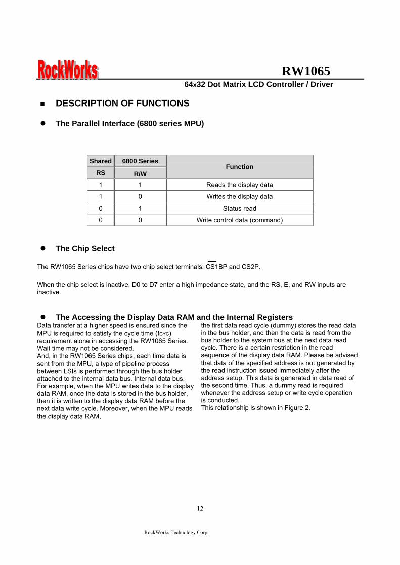
RW1065 64x32 Dot Matrix LCD Controller Driver
RockWorks Technology Corp
12
DESCRIPTION OF FUNCTIONS
The Parallel Interface (6800 series MPU)
Shared 6800 Series
RS RW Function
1 1 Reads the display data
1 0 Writes the display data
0 1 Status read
0 0 Write control data (command)
The Chip Select The RW1065 Series chips have two chip select terminals CS1
―BP and CS2P
When the chip select is inactive D0 to D7 enter a high impedance state and the RS E and RW inputs are inactive
The Accessing the Display Data RAM and the Internal Registers Data transfer at a higher speed is ensured since the MPU is required to satisfy the cycle time (tCYC) requirement alone in accessing the RW1065 Series Wait time may not be considered And in the RW1065 Series chips each time data is sent from the MPU a type of pipeline process between LSIs is performed through the bus holder attached to the internal data bus Internal data bus For example when the MPU writes data to the display data RAM once the data is stored in the bus holder then it is written to the display data RAM before the next data write cycle Moreover when the MPU reads the display data RAM
the first data read cycle (dummy) stores the read data in the bus holder and then the data is read from the bus holder to the system bus at the next data read cycle There is a certain restriction in the read sequence of the display data RAM Please be advised that data of the specified address is not generated by the read instruction issued immediately after the address setup This data is generated in data read of the second time Thus a dummy read is required whenever the address setup or write cycle operation is conducted This relationship is shown in Figure 2
RW1065 64x32 Dot Matrix LCD Controller Driver
RockWorks Technology Corp
13
E
Fig 2b read timing
E
RW
Fig 2a write timing (RW=rdquoLrdquo)
RS
RS
RW1065 64x32 Dot Matrix LCD Controller Driver
RockWorks Technology Corp
14
Display Data RAM The display data RAM is a RAM that stores the dot data for the display It has a 64 (8 page x 8 bit) x 64 bit structure It is possible to access the desired bit by specifying the page address and the column addressBecause as is shown in Figure 3 the D7 to D0 display data from the MPU corresponds to the liquid crystal display common direction there are few constraints at the time of display data transfer when multiple RW1065 series chips are used
thus and display structures can be created easily and with a high degree of freedom Moreover reading from and writing to the display RAM from the MPU side is performed through the IO buffer which is an independent operation from signal reading for the liquid crystal driver Consequently even if the display data RAM is accessed asynchronously during liquid crystal display it will not cause adverse effects on the display (such as flickering)
0
1
0
0
1
1
0
0
1
0
1
0
0
1
0
1
0
0
1
0
0
0
0
0
0
D0
D1
D2
D3
D4
-
Display data RAM Liquid crystal display
COM0
COM1
COM2
COM3
COM4
-
Figure3
The Page Address Circuit As shown in Figure 4 page address of the display data RAM is specified through the Page Address Set Command The page address must be specified again when changing pages to perform access
The Column Address As is shown in Table 4 the display data RAM column address is specified by the Column Address Set command The specified column address is incremented (+1) with each display data readwrite command This allows the MPU display data to be accessed continuously Moreover the increment of column addresses stops with 3FH Because the column address is independent of the page address when moving for example from page 0 column 3FH to page 1
column 00H it is necessary to respecify both the page address and the column address Furthermore as is shown in Table 4 the ADC command (segment driver direction select command) can be used to reverse the relationship between the display data RAM column address and the segment output Because of this the constraints on the IC layout when the LCD module is assembled can be minimized
Table 4 SEG Output
ADC set SEG0 SEG 63
ADC(D0)=0 0 rarr Column Address rarr 63 ADC(D0)=1 63 larr Column Address larr 0
RW1065 64x32 Dot Matrix LCD Controller Driver
RockWorks Technology Corp
15
Figure 4
Page Address D3 D2 D1 D0
DataSE
G0
SEG
1
SEG
2
SEG
3
SEG
4
SEG
5
SEG
6
SEG
7
SEG
8
helliphelliphelliphellip
SEG
55
SEG
56
SEG
57
SEG
58
SEG
59
SEG
60
SEG
61
SEG
62
SEG
63 SEG
COM
D0 COM0
D1 COM1
D2 COM2
D3 COM3
D4 COM4
D5 COM5
D6 COM6
0 0 0 0
D7
Page 0
COM7
D0 COM8
D1 COM9
D2 COM10
D3 COM11
D4 COM12
D5 COM13
D6 COM14
0 0 0 1
D7
Page 1
COM15
D0 COM16
D1 COM17
D2 COM18
D3 COM19
D4 COM20
D5 COM21
D6 COM22
0 0 1 0
D7
Page 2
COM23
D0 COM24
D1 COM25
D2 COM26
D3 COM27
D4 COM28
D5 COM29
D6 COM30
0 0 1 1
D7
Page 3
COM31
ADC=0 00
01
02
03
04
05
06
07
08
helliphelliphelliphellip 55
56
57
58
59
60
61
62
63
COLUMN ADC=1 63
62
61
60
59
58
57
56
55
helliphelliphelliphellip 08
07
06
05
04
03
02
01
00
RW1065 64x32 Dot Matrix LCD Controller Driver
RockWorks Technology Corp
16
Common Timing Generator Circuit Display Data Latch Circuit Generates common timing signals and FR frame signals from the CL basic clock The 132 or 164 duty (for RW1065) can be selected by the Duty Select command The 132 and 164 duties are provided by two chips consisting of the master and slave chips in the common multi-chip mode
This latch stores one line of display data for use by the LCD driver interface circuitry The output of this latch is controlled by the Display ONOFF
132 duty
164 duty
SHL=0
SHL=1
SHL=0
SHL=1
RW1065 64x32 Dot Matrix LCD Controller Driver
RockWorks Technology Corp
17
Display Timing Generator Circuit
The display timing generator circuit generates the timing signal to the line address circuit and the display data latch circuit using the display clock The display data is latched into the display data latch circuit synchronized with the display clock and is output to the data driver output terminal Reading to the display data liquid crystal driver circuits is completely independent of accesses to the display data RAM by the MPU Consequently even if the display data
RAM is accessed asynchronously during liquid crystal display there is absolutely no adverse effect (such asflickering) on the display Moreover the display timing generator circuit generates the common timing and the liquid crystal alternating current signal (FR) from the display clock It generates a drive wave form using a 2 frame alternating current drive method as is shown in Figure 5 for the liquid crystal drive circuit
Two-frame alternating current drive waveform
Figure 5
When multiple RW1065 Series chips are used the slave chip must be supplied the display timing signals(FR CL) from the master chip
Table 5 shows the status of the FR and CL signals
Table 5 Operating Mode FR CL
Master (MS = ldquoHrdquo) The internal oscillator circuit is enabled (CLS = ldquoHrdquo) The internal oscillator circuit is disabled (CLS = ldquoLrdquo)
Output Output
Output Input
Slave (MS = ldquoLrdquo) The internal oscillator circuit is enabled (CLS = ldquoHrdquo) The internal oscillator circuit is disabled (CLS = ldquoLrdquo)
Input Input
Input Input
RW1065 64x32 Dot Matrix LCD Controller Driver
RockWorks Technology Corp
18
The Liquid Crystal Driver Circuits
These are a 64-channel (RW1065) that generate four voltage levels for driving the liquid crystal The combination of the display data the COM scan signal and the FR signal
produces the liquid crystal drive voltage output Figure 6 shows examples of the SEG and COM output waveform
Figure 6
RW1065 64x32 Dot Matrix LCD Controller Driver
RockWorks Technology Corp
19
The Power Supply Circuit
The power supply circuits are low-power consumption power supply circuits that generate the voltage levels required for the liquid crystal drivers They comprise Booster circuits and voltage follower circuits They are only enabled in master operation The power supply circuits can turn on automatically after power on
Consequently it is possible to make an external power supply and the internal power supply function somewhat in parallel
The Liquid Crystal Voltage Generator Circuit The V0 voltage is produced by a resistive voltage divider outside the IC through VRAB pin and can be produced at the V1 V2 V3 and V4 voltage levels required for liquid crystal driving Moreover when the voltage follower changes the impedance it provides V1 V2 V3 and V4 to the liquid crystal drive circuit 15 bias or 16 bias or 18 bias or 19 bias for RW1065 can be selected by BS0 and BS1 pins V0-Vss maximum voltage is 15V Vout-Vss maximum voltage is 17V If VDD lt 35V it can use the Booster circuit 2x3x4xThe booster voltage can follow the spec condition (Vout-Vss ≦ 17V max voltage) if VDD gt35V only use the 2X3X booster circuit that can ensure the V0-Vss voltage ≦ 15V If use the VDD voltage 5V and 4X booster itrsquos over the spec operation condition To turn on built-in power (boosterfollower) must waiting 200mS to display on for boosterfollower stable Therefore power off must follower ldquopower off sequencerdquo too
Power on Display off
Power off
Power off sequence
Wait time gt200mS
Display on
Power on sequence
RW1065 64x32 Dot Matrix LCD Controller Driver
RockWorks Technology Corp
20
The Reset Circuit
When the RTP input comes to the ldquoLrdquo level these LSIs return to the default state Their default states are as follows 1 Display OFF 2 Display all point on is select to normal 3 Display normalreverse is select to normal 4 164 duty is selected 5 Read modify write OFF 6 Column address set to Address 0 7 Page address set to Page 0 8 Start line set to first line 9 Frame frequency set to default 10 Power save mode released 11 Ext set to ldquo0rdquo When the power is turned on the IC internal state becomes unstable and it is necessary to initialize it using the RSTP terminal After the initialization each input terminal should be controlled normally While RSTP is ldquoLrdquo the oscillator works but the display timing generator stops and the CL FR terminals are fixed to ldquoHrdquo The terminals D0 to D7 are not affected
RW1065 64x32 Dot Matrix LCD Controller Driver
RockWorks Technology Corp
21
TABLE OF RW1065 INSTRUCTIONS
Instruction code Instruction RS RW DB7 DB6 DB5 DB4 DB3 DB2 DB1 DB0 Description
EXT=0 or 1
MODE SET 0 0 0 0 0 0 1 1 0 EXT Set EXT mode
Instruction code Instruction RS RW DB7 DB6 DB5 DB4 DB3 DB2 DB1 DB0 Description
EXT=0 Display ONOFF 0 0 0 0 1 1 1 1 1 D D=0Display OFF
D=1Display ONSet page address 0 0 1 0 1 1 1 P2 P1 P0 Set page address
Set column address 0 0 0 1 Y5 Y4 Y3 Y2 Y1 Y0 Set column
address MSB
Read Status 0 1 BUSY 0 ON OFF RESET 0 0 0 0 Read register
status Write display
data 1 0 Write data Write data into DDRAM
Read display data 1 1 Read data Read data from
DDRAM Set initial
display line register
0 0 1 1 S5 S4 S3 S2 S1 S0 Specify the initial
display line to realize vertical scrolling
Instruction code Instruction RS RW DB7 DB6 DB5 DB4 DB3 DB2 DB1 DB0 Description
EXT=1
NOP 0 0 0 0 0 0 0 0 0 0 no operation
Set modiy-read 0 0 0 0 0 0 1 0 0 0 Set modiy-read
mode
END 0 0 0 0 0 0 1 1 1 0 release modiy-read mode
Set power save mode 0 0 0 0 0 0 0 0 1 PSAVE P=0 normal mode
P=1 sleep mode
0 0 0 0 0 1 0 1 Display
COMMAND (double
command)
0 0 FRSEL
0 0 0 0 REV ALLON DUTY
DUTY=1 64 duty DUTY=0 32 duty ALLON=1display all on ALLON=0display
normal REV=1display reverse REV=0display normal FRSEL=1FR frequency double default FRSEL=0FR frequency default
RW1065 64x32 Dot Matrix LCD Controller Driver
RockWorks Technology Corp
22
Command Description
See the Table of RW1065 instructions The RW1065 series identifies a data bus using a combination of RS E and RW signals As the MPU translates a command in the internal timing only (independent from the external clock) its speed is very high The busy check is usually not required
Display ONOFF
EXT RS RW D7 D6 D5 D4 D3 D2 D1 D0
0 0 0 0 0 1 1 1 1 1 D
This command turns the display on and off D=1 Display ON D=0 Display OFF(default)
Set page Address This command specifies the page address that corresponds to the low address of the display data RAM when it is accessed by the MPU Any bit of the display data RAM can be accessed when its page address and column address are specified The display status is not changed even when the page address is changed
EXT RS RW D7 D6 D5 D4 D3 D2 D1 D0
0 0 0 1 0 1 1 1 A2 A1 A0
This command loads the page address register
A2 A1 A0 Page
0 0 0 0 (default)
0 0 1 1 0 1 0 2 0 1 1 3 1 0 0 4 1 0 1 5 1 1 0 6 1 1 1 7
Page mapping see Figure 4
RW1065 64x32 Dot Matrix LCD Controller Driver
RockWorks Technology Corp
23
Set Column Address This command specifies a column address of the display data RAM When the display data RAM is accessed by the MPU continuously the column address is incremented by I each time it is accessed from the set address Therefore the MPU can access to data continuously The column address stops to be incremented at address 63 and the page address is not changed continuously
EXT RS RW D7 D6 D5 D4 D3 D2 D1 D0
0 0 0 0 1 A5 A4 A3 A2 A1 A0
A5 A4 A3 A2 A1 A0 Column Address0 0 0 0 0 0 0(default) 0 0 0 0 0 1 1
1 1 1 1 1 1 63
Read Status
EXT RS RW D7 D6 D5 D4 D3 D2 D1 D0
0 0 1 BUSY 0 ON OFF RESET 0 0 0 0
The BUSY Flag bit indicates that RW 1065 is operating or no operating
BUSY=1 Operation BUSY=0 Ready
The ONOFF bit indicates the current status of the display It is the inverse of the polarity of the display ONOFF command ONOFF=1 Display OFF ONOFF=0 Display ON The RESET bit indicates whether the driver is executing a hardware or software reset or if it is in normal operating mode RESET=1 Currently executing reset command RESET=0 Normal operation
RW1065 64x32 Dot Matrix LCD Controller Driver
RockWorks Technology Corp
24
Write Display Data
EXT RS RW D7 D6 D5 D4 D3 D2 D1 D0
0 1 0 Write data
Writes 8-bits of data into the display data RAM at a location specified by the contents of the column address and page address registers and then increments the column address register by one
Read Display Data
EXT RS RW D7 D6 D5 D4 D3 D2 D1 D0
0 1 1 Read data
Reads 8-bits of data from the data IO latch updates the contents of the IO latch with display data from the display data RAM location specified by the contents of the column address and page address registers and then increments the column address register After loading a new address into the column address register one dummy read is required before valid data is obtained
Set initial display line register
EXT RS RW D7 D6 D5 D4 D3 D2 D1 D0
0 0 0 1 1 S5 S4 S3 S2 S1 S0
Loads the RAM line address of the initial display line COM 0 into the initial display line register The RAM display data becomes the top line of the LCD screen It is followed by the higher number lines in ascending order corresponding to the duty cycle The screen can be scrolled using this command by incrementing the line address(default value=rdquo00Hrdquo)
RW1065 64x32 Dot Matrix LCD Controller Driver
RockWorks Technology Corp
25
Read-Modify-Write
EXT RS RW D7 D6 D5 D4 D3 D2 D1 D0
1 0 0 0 0 0 0 1 0 0 0
This command defeats column address register auto-increment after data reads The current contents of the column Address register are saved The mode remains active until an End command is received When the End command is entered the column address is returned to the one used during input of Read-Modify-Write Command This function can reduce the load of MPU when data change is repeated as a specific display area Any command other than Data Read or Write can be used in the Read-Modify-Write mode However the Column Address Set command cannot be used
End
EXT RS RW D7 D6 D5 D4 D3 D2 D1 D0
1 0 0 0 0 0 0 1 1 1 0
This command cancels read-modify-write mode and restores the contents of the column address register to their value prior to the receipt of the Read-Modify-Write command
N N+1 N+2 N+3 N+m N
Read -modify-write mode set End
Returm
Column address
Set page address
Set column address
Read-modify-write
Dummy read
Read data
Write data
End
CompletedNo
Yes
RW1065 64x32 Dot Matrix LCD Controller Driver
RockWorks Technology Corp
26
Set power save mode
EXT RS RW D7 D6 D5 D4 D3 D2 D1 D0
1 0 0 0 0 0 0 0 0 1 PSAVE
When power save mode is entered thus greatly reducing power consumption In the power save mode the display data is saved as is the operating mode that was in effect before the power saver mode was initiated and the MPU is still able to access the display data RAM PSAVE=1 Sleep mode PSAVE=0 Normal mode Sleep mode This stops all operations in the LCD display system and as long as there are no accesses from the MPU the consumption current is reduced to a value near the static current The internal modes during sleep mode are as follows 1 The oscillator circuit and the LCD power supply circuit are halted 2 All liquid crystal drive circuits are halted and the segment and common drive outputs output a Vss level
Display command double command
EXT RS RW D7 D6 D5 D4 D3 D2 D1 D0
1 0 0 0 0 0 0 0 1 0 1
1 0 0 FRSEL 0 0 0 0 REV ALLON DUTY
Display NormalReverse set REV=1 Reverse REV=0 Normal(default) Display All Point ONOFF ALLON=1 All display points ON ALLON=0 Normal(default) Select Duty Duty=1 164 duty cycle(default) Duty=0 132 duty cycle FRAME FREQUENCY Select FRSEL=1 Double FRSEL=0 (default)
RW1065 64x32 Dot Matrix LCD Controller Driver
RockWorks Technology Corp
27
Hardware Pin Set
Select ADC by ADC Pin The pin selects the relationship between display data RAM column addresses and segment drivers ADC=1 SEG0larrcolumn address 3FHhellipinverted ADC=0 SEG0larrcolumn address 00Hhellipnormal(default) This command is provided to reduce restrictions on the placement of driver ICs and routing of traces during printed circuit Board design See Figure 4 for a table of segments and column addresses for the two values of D
Select SHL by SHL Pin The pin selects the com output scan direction SHL=1 Reverse directioncom63rarrcom0 SHL=0 Normal com0rarrcom63 Both master and slave should set identical SHL value
Select LCD Bias by BS0 BS1 Pin
BS1 BS0 Bias 0 0 15 bias 0 1 16 bias 1 0 18 bias 1 1 19 bias
RW1065 64x32 Dot Matrix LCD Controller Driver
RockWorks Technology Corp
28
When an External Resistance is Used The liquid crystal power supply voltage V0 is set by adding resistors Rarsquo and Rbrsquo between VDD and VR and between VR and V0 respectively
RW1065
RW1065 64x32 Dot Matrix LCD Controller Driver
RockWorks Technology Corp
29
The set voltage circuits
Using the step-up voltage circuits equipped within the RW1065 chips it is possible to produce a 2X 3X 4X step-up voltage levels 2X step-up
To produce voltage level in the positive direction at the Vout terminal that is 2 times the voltage difference between VSS and VDD2 Please configure set voltage circuits like this Place a 1uF~22uF capacitor between CAP1N and CAP1P Place a 1uF~22uF capacitor between VSS and VOUT Short CAP2P CAP3P and VOUT Leave CAP2N open 3X step-up
To produce voltage level in the positive direction at the Vout terminal that is 3 times the voltage difference between VSS and VDD2 Please configure set voltage circuits like this Place a 1uF~22uF capacitor between CAP1N and CAP1P Place a 1uF~22uF capacitor between VSS and VOUT Place a 1uF~22uF capacitor and 100 ohms resistor between CAP2N and CAP2P Short CAP3P and Vout 4X step-up
To produce voltage level in the positive direction at the Vout terminal that is 4 times the voltage difference between VSS and VDD2 Please configure set voltage circuits like this Place a 1uF~22uF capacitor between CAP1N and CAP1P Place a 1uF~22uF capacitor between VSS and VOUT Place a 1uF~22uF capacitor and 100 ohms resistor between CAP2N and CAP2P Place a 1uF~22uF capacitor and 100 ohms resistor between CAP1N and CAP3P
RW1065 64x32 Dot Matrix LCD Controller Driver
RockWorks Technology Corp
30
ABSOLUTE MAXIMUM RATINGS Characteristics Symbol Value Unit
Power supply voltage VDD -03 to +70 V
LCD driver voltage Vout 0 to +17 V
Input voltage VIN -03 to VDD+03 V
Operating temperature TA -40 to +85
Storage temperature TSTO -55 to +125
DC CHARACTERISTICS
Rating Item Symbol Condition Min Typ Max Unit ApplicablePin
Operating Voltage VDD - 27 30 55 V VDD1
Step up output voltage Vout (Relative to VDD) 0 - 17 V Vout
Voltage follower circuit operating Voltage V0 (Relative to VDD) 0 - 15 V V0
V0 accuracy V0 - 0 - 15 V0
High-level Input Voltage Low-level Input Voltage
VIHC VILC - 07 VDD
Vss - VDD 09 V 2
High-level Output Voltage Low-level Output Voltage
VOHC VOLC
IOH = ndash05 mA IOL = 05 mA
08VDD Vss - VDD
02 VDD V 3
Input leakage current ILI VIN = VDD or VSS -1 - 2 uA 4
Output leakage current ILO - -1 1 uA 5
Liquid Crystal Driver ON Resistance RON
Ta= 25degC(Relative To VDD)
V0 =15 V - 16 20 KΩ SEGn COMn 6
Internal Oscillator fOSC 2286 254 2794 Oscillator
Frequency External Input RECOMMAND fCL
Ta = 25degC 132Duty 2286 254 2794
kHz CL
Internal Oscillator fOSC 45 5 55 Oscillator
Frequency External Input RECOMMAND fCL
Ta = 25degC 164Duty 45 5 55
kHz CL
bullDynamic Consumption Current During Display with the Internal Power Supply OFF Current consumed by total ICs when an external power supply is used
Unless otherwise specified Vss=0V VDD=30V
RW1065 64x32 Dot Matrix LCD Controller Driver
RockWorks Technology Corp
31
Display Pattern OFF
Ta = 25degC Vout=17V Rating Item Symbol Condition Min Typ Max Unit Notes
VDD=30 V V0-Vss=8V - 10 15 RW1065 IDD VDD=50 V V0-Vss=8V - 35 45
microA 7
Display Pattern Checker
Ta = 25degC Vout=17V Rating Item Symbol Condition Min Typ Max Unit Notes
VDD=30 V V0-Vss=8V - 15 20 RW1065 IDD VDD=50 V V0-Vss=8V - 40 50
microA 7
Display Pattern OFF
Ta = 25degC Vout=17V Rating Item Symbol Condition Min Typ Max Unit Notes
VDD=30 V V0-Vss=8V - 15 20 RW1065 IDD VDD=50 V V0-Vss=8V - 40 50
microA 7
Display pattern Checker
Ta = 25degC Vout=17V Rating Item Symbol Condition Min Typ Max Unit Notes
VDD=30 V V0-Vss=8V - 65 80 RW1065 IDD VDD=50 V V0-Vss=8V - 130 150
microA 7
bull Consumption Current at Time of Power Saver Mode VSS = 0 V VDD = 30 V plusmn 10
Rating Item Symbol Condition Min Typ Max Unit Notes
Sleep mode IDD - - 5 10 microA -
References for items market with 1 While a broad range of operating voltages is guaranteed performance cannot be guaranteed if there are sudden fluctuations to the
voltage while the MPU is being accessed 2 The RS D0 to D5 D6 D7 E RW CS1BP CS2P CLS CL FR MS and RST
― terminals
3 The D0 to D7 FR and CL terminals 4 The RS E RW CS1BP CS2P CLS MS and RST
― terminals
5 Applies when the D0 to D5 D6 D7 CL and FR terminals are in a high impedance state 6 These are the resistance values for when a 01 V voltage is applied between the output terminals SEGn or COMn and
the various power supply terminals (V1 V2 V3 and V4) These are specified for the operating voltage (3) range RON = 01 V ∆I (Where ∆I is the current that flows when 01 V is applied while the power supply is ON)
7 It indicates the current consumed on ICs alone when the internal oscillator circuit and display are turned on Does not include the current due to the LCD panel capacity and wiring capacity Applicable only when there is no access from the MPU
RW1065 64x32 Dot Matrix LCD Controller Driver
RockWorks Technology Corp
32
TIMING CHARACTERISTICS
68 Interface
(Ta=-40 to 85 degC) VDD=27 to 45V
Rating VDD=45 to 55V
Rating Item Signal Symbol ConditionMin Max Min Max
Units
Address hold time RS tAH6 0 mdash 0 mdash Address setup time RS tAW6
mdash 0 mdash 0 mdash
ns
System cycle time RS tCYC6 mdash 900 mdash 800 mdash ns Data setup time D0 to D7 tDS6 100 mdash 100 mdash Data hold time D0 to D7 tDH6
mdash 0 mdash 0 mdash
ns
Access time D0 to D7 tACC6 mdash 350 mdash 250
Output disable time D0 to D7 tOH6 CL = 100 pF
mdash 300 mdash 200 ns
Read tEWHR 360 mdash 300 mdash Enable H pulse time
WriteE
tEWHW mdash
360 mdash 300 mdash ns
Read tEWLR 450 mdash 400 mdash Enable L pulse time
WriteE
tEWLW mdash
450 mdash 400 mdash ns
1 All timing is specified using 20 and 80 of VDD as the reference 2 tEWLW and tEWLR are specified as the overlap between CS1BP being ldquoLrdquo (CS2P = ldquoHrdquo) and E
RW1065 64x32 Dot Matrix LCD Controller Driver
RockWorks Technology Corp
33
Reset Timing
Rating Item Signal Symbol Condition
Min Typ Max Units
Reset time mdash tR mdash mdash - 2 micros
Reset ldquoLrdquo pulse width RST tRW mdash 2 - mdash micros
1 When double chip was be used then the duty set command must be set between the tR
RW1065 64x32 Dot Matrix LCD Controller Driver
RockWorks Technology Corp
34
IO PAD CONFIGURATION
RW1065 64x32 Dot Matrix LCD Controller Driver
RockWorks Technology Corp
35
THE MPU INTERFACE (REFERENCE EXAMPLES) The RW1065 Series can be connected to 6800 Series MPUs The display area can be enlarged by using multiple RW1065 Series chips When this is done the chip select signal can be used to select the individual ICs to access
6800 Series MPUs
RW
106
5
RW1065 64x32 Dot Matrix LCD Controller Driver
RockWorks Technology Corp
36
When using external multi-level power supply for LCD driving (REFERENCE EXAMPLE)
Using a resistor divider can provide RW1065 external multi-level power supply for LCD driving
The circuit below shows a resistor divider network which can bias V0 V1 V2 V3 and V4 externally
RW1065 64x32 Dot Matrix LCD Controller Driver
RockWorks Technology Corp
37
bullWhen V0 V1 V2 V3 and V4 are biased by external power supply analog section of RW1065 should be turn off by software during LCD initialization The example in below shows the sequence to turn off analog section when external bias is used Begin of LCD initialization 1 Reset RW1065 2 SET EXT=1 (mode instruction)
RS RW DB7 DB6 DB5 DB4 DB3 DB2 DB1 DB00 0 0 0 0 0 1 1 0 1
3 SET Display Command (double command)
RS RW DB7 DB6 DB5 DB4 DB3 DB2 DB1 DB00 0 0 0 0 0 0 1 0 1 0 0 0 0 1 1 0 0 0 1
4 SET EXT=1 (mode instruction)
RS RW DB7 DB6 DB5 DB4 DB3 DB2 DB1 DB00 0 0 0 0 0 1 1 0 0
End of LCD initialization
bullBecause pins can not set LCD bias when external power supplies are used for LCD driving the bias can be set by an appropriate configuration for a resistor voltage divider networks The example is shown below
VSS
R
R
NR
R
R
RV1
RV2
RV3
RV4
V0
Bias Network Circuit Concept 15 Bias N=1 total = 5R 16 Bias N=2 total =6R 18 Bias N=4 total =8R 19 Bias N=5 total = 9R
RW1065 64x32 Dot Matrix LCD Controller Driver
RockWorks Technology Corp
38
Single chip solution for RW1065 application (REFERENCE EXAMPLE)
For a 64x32 application the duty cycle of LCD panel is 164 and the display duty of RW1065 should be set to 164 The display duty cycle can be selected by the DUTY bit in display command The diagram for 64x32 application is shown below
64 SEGx32COM LCD Panel
164 duty cycle
RW1065 DUTY=1
COM1~33
SEG1~65
RW1065 64x32 Dot Matrix LCD Controller Driver
RockWorks Technology Corp
39
Using an adjustable resistor on the main board to adjust the contrast of liquid crystal display (REFERENCE EXAMPLE)
The schematic shows an adjustable resistor on main board that can adjust voltage level of V0
RW1065 64x32 Dot Matrix LCD Controller Driver
RockWorks Technology Corp
40
Package information (Please pay close attention to the information in this section Do not hesitate to consult with our sale representative if you have any question or concern)
In order to make better bonding yield for RW1065 please follow the tips and recommendations in this section In this section few tips about COB footprint style PCB layout and wire bonding will be discussed
The drawing in below shows the PCB footprint style which we recommend for RW1065 Pads array in
curve shape is easier for Al wire bonding Besides that a real size COB footprint for RW1065 is also shown in below RW1065 COB footprint is also available in powerpcb or protel format for design reference purpose
The ratio is 11
RW1065 64x32 Dot Matrix LCD Controller Driver
RockWorks Technology Corp
41
During COB footprint design there have some tips about footprint that the PCB designer should know The angle between bonding wire and vertical line should less than 45 Otherwise the wire shorts would become very easy to happen at fours corners of the chip
The angle between bonding wire and vertical line could be reduced by expanding the distance between pads array and the chip In addition reducing length in horizon direction of pads array could minimize the angle between bonding wire and vertical line The picture in below will help to illustrate this concept From the experiences COB footprint style affects the bonding yield
Bad Wires are too close to each other
The angle between bonding wire and vertical line is greater than 45
The angle between bonding wire and vertical line is less than 45
Wires are not too close to each other
Reducing length in horizon direction of pads array could minimize the angle between bonding wire and vertical line
The angle between bonding wire and vertical line could be reduced by expanding the distance between pads array and the chip
RW1065 64x32 Dot Matrix LCD Controller Driver
RockWorks Technology Corp
42
If the gap between pads of COB footprint is filled with solder mask coating it is difficult to bond Al wire to
the pads The top solder masks layer that overlap COB footprint area should be removed
Please use 1 mils diameter Al wire for RW1065 wire bonding
1 2 3 4 5 6
A
B
C
D
654321
D
C
B
A
Title
Number RevisionSize
C
Date 29-Aug-2007 Sheet of File D公司資料99seMyDesignddb Drawn By
RW1065
COM131
COM142
COM153
COM164
COM175
COM186
COM197
COM208
COM219
COM2210
COM2311
COM2412
COM2513
COM2614
COM2715
COM2816
COM2917
COM3018
COM3119
SEG
6320
SEG
6221
SEG
6122
SEG
6023
SEG
5924
SEG
5825
SEG
5726
SEG
5627
SEG
5528
SEG
5429
SEG
5330
SEG
5231
SEG
5132
SEG
5033
SEG
4934
SEG
4835
SEG
4736
SEG
4637
SEG
4538
SEG
4439
SEG
4340
SEG
4241
SEG
4142
SEG
4043
SEG
3944
SEG
3845
SEG
3746
SEG
3647
SEG
3548
SEG
3449
SEG
3350
SEG
3251
SEG
3152
SEG
3053
SEG
2954
SEG
2855
SEG
2756
SEG
2657
SEG
2558
SEG
2459
SEG
2360
SEG
2261
SEG
2162
SEG
2063
SEG
1964
SEG
1865
SEG
1766
SEG
1667
SEG
1568
SEG
1469
SEG13 70SEG12 71SEG11 72SEG10 73SEG9 74SEG8 75SEG7 76SEG6 77SEG5 78SEG4 79SEG3 80SEG2 81SEG1 82SEG0 83ADCP 84CLL 85
VSS
86D
087
D1
88D
289
D3
90D
491
D5
92D
693
D7
94C
S1B
P95
CS2
P96
ERD
P97
AO
P(R
S)98
RW
RP
99V
DD
100
RST
P10
1C
LSP
102
FRR
103
MSP
104
BS1
P10
5B
S0P
106
SHLP
107
VD
D2
108
CA
P2N
109
CA
P2P
110
CA
P1P
111
CA
P1N
112
CA
P3P
113
VO
UT
114
V0
115
VR
AB
116
V3
117
V2
118
V4
119
V1
120
CO
M0
121
CO
M1
122
CO
M2
123
CO
M3
124
CO
M4
125
CO
M5
126
CO
M6
127
CO
M7
128
CO
M8
129
CO
M9
130
CO
M10
131
CO
M11
132
CO
M12
133
4897x1902 um
IC1
RW1065
C9CAPR4
100R0603
R30R0603
C8
CAP
C7
CAP
R2
100R0603
R1
0R0603C6 22uf
R50R
R6300R
R7RES1
R8NC R9
100R0603
VDD
R10
NC
R11
100R0603
R12
100R0603
R13
NC
R14
100R0603
R15
NC
VDD
D0
D1
D2
D3
D4
D5
D6
D7
DB[07]
VDDC5
01uf0603
VD
D
CS2
P
123456789
1011121314151617181920
J1
CON20
C1201uf0603
R3951K0603
VDD
CAP Value1UF~22UF
2XPut C6C8 Short R1R3Open R2R4C7C93XPut C6C8C9 R4Short R1Open R2R3C74XOpen R1R3
BS0 BS1 Bias0 0
0 1
1 0
11
15 bias
16 bias
18 bias
19 bias
ADC=0 SEG0lt~column address 00Hnormal(default) ADC=1 SEG0lt~column address 3FHinverted
SHL=0 Normal COM0~gtCOM63(default)SHL=1 Reverse direction COM63~gtCOM0
R16100R0603
LCD PANEL 64X32RockWorks
RW1065 64X32
COM0-31 SEG0-63SHL=0 ADC=0
SHL=1COM31-0
ADC=1SEG63-0
if use single chip for 32 command displaythe display command must select 164 dutyDisplay panel must select 164 duty type
VO
UT
C3P
C1N
C1P
C2P
C2N
VDD2
ADC
SHL
BS0
BS1
CLLADC
V1
V2
V3
V4
VR
AB
V0
VO
UT
C3P
C1N
C1P
C2P
C2N
VD
D2
SHL
BS0
BS1
FRR
RST
P
RW
RS
E CS1
B
CS1
V0RSRWED0D1D2D3D4D5D6D7
RSTPAK
C4
22uf
RBRES1
RA1RES1
C2
22uf
C1
22uf
C3
22uf
C0
22uf
R20
100k0603
R21
100k0603
R17
200K0603
V1
V2
V3
V4 VRAB
V0
V0
OPTION
B
R18
300R0603
RA2RES1
VADJ
R19100R
R23 RES1R22 0R
R24
RES1
R25
0R
VDD
CS1BP
CS2P
CS1
CS1
R26
22R0603
R27
22R0603
C1047uf
C11
01uf
VSS_INVDD_IN
D1DIODE
FGND
鐵框地
VSS
VDD
R28 10RR29 10RR30 10RR31 10RR32 10RR33 10RR34 10RR35 10RR36 10RR37 10RR38 10R
VADJ
1 2 3 4 5 6
A
B
C
D
654321
D
C
B
A
Title
Number RevisionSize
C
Date 29-Aug-2007 Sheet of File D公司資料99seMyDesignddb Drawn By
RW1065
COM131
COM142
COM153
COM164
COM175
COM186
COM197
COM208
COM219
COM2210
COM2311
COM2412
COM2513
COM2614
COM2715
COM2816
COM2917
COM3018
COM3119
SEG
6320
SEG
6221
SEG
6122
SEG
6023
SEG
5924
SEG
5825
SEG
5726
SEG
5627
SEG
5528
SEG
5429
SEG
5330
SEG
5231
SEG
5132
SEG
5033
SEG
4934
SEG
4835
SEG
4736
SEG
4637
SEG
4538
SEG
4439
SEG
4340
SEG
4241
SEG
4142
SEG
4043
SEG
3944
SEG
3845
SEG
3746
SEG
3647
SEG
3548
SEG
3449
SEG
3350
SEG
3251
SEG
3152
SEG
3053
SEG
2954
SEG
2855
SEG
2756
SEG
2657
SEG
2558
SEG
2459
SEG
2360
SEG
2261
SEG
2162
SEG
2063
SEG
1964
SEG
1865
SEG
1766
SEG
1667
SEG
1568
SEG
1469
SEG13 70SEG12 71SEG11 72SEG10 73SEG9 74SEG8 75SEG7 76SEG6 77SEG5 78SEG4 79SEG3 80SEG2 81SEG1 82SEG0 83ADCP 84CLL 85
VSS
86D
087
D1
88D
289
D3
90D
491
D5
92D
693
D7
94C
S1B
P95
CS2
P96
ERD
P97
AO
P(R
S)98
RW
RP
99V
DD
100
RST
P10
1C
LSP
102
FRR
103
MSP
104
BS1
P10
5B
S0P
106
SHLP
107
VD
D2
108
CA
P2N
109
CA
P2P
110
CA
P1P
111
CA
P1N
112
CA
P3P
113
VO
UT
114
V0
115
VR
AB
116
V3
117
V2
118
V4
119
V1
120
CO
M0
121
CO
M1
122
CO
M2
123
CO
M3
124
CO
M4
125
CO
M5
126
CO
M6
127
CO
M7
128
CO
M8
129
CO
M9
130
CO
M10
131
CO
M11
132
CO
M12
133
4897x1902 um
IC1
RW1065 Master
RW1065
COM131
COM142
COM153
COM164
COM175
COM186
COM197
COM208
COM219
COM2210
COM2311
COM2412
COM2513
COM2614
COM2715
COM2816
COM2917
COM3018
COM3119
SEG
6320
SEG
6221
SEG
6122
SEG
6023
SEG
5924
SEG
5825
SEG
5726
SEG
5627
SEG
5528
SEG
5429
SEG
5330
SEG
5231
SEG
5132
SEG
5033
SEG
4934
SEG
4835
SEG
4736
SEG
4637
SEG
4538
SEG
4439
SEG
4340
SEG
4241
SEG
4142
SEG
4043
SEG
3944
SEG
3845
SEG
3746
SEG
3647
SEG
3548
SEG
3449
SEG
3350
SEG
3251
SEG
3152
SEG
3053
SEG
2954
SEG
2855
SEG
2756
SEG
2657
SEG
2558
SEG
2459
SEG
2360
SEG
2261
SEG
2162
SEG
2063
SEG
1964
SEG
1865
SEG
1766
SEG
1667
SEG
1568
SEG
1469
SEG13 70SEG12 71SEG11 72SEG10 73SEG9 74SEG8 75SEG7 76SEG6 77SEG5 78SEG4 79SEG3 80SEG2 81SEG1 82SEG0 83ADCP 84CLL 85
VSS
86D
087
D1
88D
289
D3
90D
491
D5
92D
693
D7
94C
S1B
P95
CS2
P96
ERD
P97
AO
P(R
S)98
RW
RP
99V
DD
100
RST
P10
1C
LSP
102
FRR
103
MSP
104
BS1
P10
5B
S0P
106
SHLP
107
VD
D2
108
CA
P2N
109
CA
P2P
110
CA
P1P
111
CA
P1N
112
CA
P3P
113
VO
UT
114
V0
115
VR
AB
116
V3
117
V2
118
V4
119
V1
120
CO
M0
121
CO
M1
122
CO
M2
123
CO
M3
124
CO
M4
125
CO
M5
126
CO
M6
127
CO
M7
128
CO
M8
129
CO
M9
130
CO
M10
131
CO
M11
132
CO
M12
133
4897x1902 um
IC2
RW1065 Slave
C4
22uf
RBRES1
RA1RES1
C2
22uf
C1
22uf
C3
22uf
C0
22ufC9CAPR4
100R0603
R30R0603
C8
CAP
C7
CAP
R2
100R0603
R1
0R0603C6 22uf
R50R0603
R6300R0603
R7RES1
R8NC R9
100R0603
VDD
R10
NC
R11
100R0603
R12
NC
R13
100R0603
R14
100R0603
R15
NC
R16
100R0603
R17
NC
VDD
D0
D1
D2
D3
D4
D5
D6
D7
D0
D1
D2
D3
D4
D5
D6
D7
DB[07] DB[07]
VDDC10
01uf0603
VD
D
IC1_
CS2
P
VDD
IC2_
CS2
P
VD
D
C11
01uf0603
VSS
VSS
LCD PANEL 128X64
Master COM0-31 Slave COM32-63
Master SEG0-63 Slave SEG64-127
123456789
1011121314151617181920
J1
CON20
Master Slave
CAP Value1UF~22UF
2XPut C6C8 Short R1R3Open R2R4C7C93XPut C6C8C9 R4Short R1Open R2R3C74XOpen R1R3
RockWorksRW1065 128x64
BS0 BS1 Bias0 0
0 1
1 0
11
15 bias
16 bias
18 bias
19 bias
ADC=0 SEG0lt~column address 00Hnormal(default) ADC=1 SEG0lt~column address 3FHinverted
SHL=0 Normal COM0~gtCOM63(default)SHL=1 Reverse direction COM63~gtCOM0Both Master and Slave should set identical SHL value
SHL=0 SHL=0
ADC=0 ADC=0
Slave COM31-0
Slave SEG127-64
SHL=1
ADC=1
SHL=1Master COM63-32
ADC=1Master SEG63-0
R18100R0603
R22
100k0603
R23
100k0603
C501uF0603
R4551K0603
VDD
R19
200K0603
ADC1
ADC2
SHL
BS0
BS1
VDD2
V1
V2
V3
V4 VRAB
V0
V0V
OU
T
C3P
C1N
C1P
C2P
C2N
V1
V2
V3
V4
VR
AB
V0
VO
UT
C3P
C1N
C1P
C2P
C2N
VD
D2
SHL
BS0
BS1
FRR
RST
P
RW
RS
E IC1_
CS1
BP
V1
V2
V3
V4
VR
AB
V0
VO
UT
VD
D2
SHL
BS0
BS1
FRR
RST
P
RW
RS
E IC2_
CS1
BP
CLLADC1
CLLADC2
RSTP
CS1CS2
V0RSRWED0D1D2D3D4D5D6D7
AK
OPTION
R20
300R0603
RA2RES1
VADJ
R21
100R
B
R25 RESR24 0R
R26 RES R27 0RVDD
IC1_CS1BP
IC1_CS2P
CS1
CS1
R28 0R R29 RES
R30 RES R31 0R
IC2_CS1BP
IC2_CS2P
CS2
CS2
R32
22R0603
R33
22R0603
C1001uf
C11
47uf
D1DIODE
FGND
鐵框地
VSS
VDD
R34 10RR35 10RR36 10RR37 10RR38 10RR39 10RR40 10RR41 10RR42 10RR43 10RR44 10R
VSS_INVDD_IN
VADJ
VDD
1 2 3 4 5 6 7 8
A
B
C
D
87654321
D
C
B
A
Title
Number RevisionSize
D
Date 29-Aug-2007 Sheet of File D公司資料 99seMyDesignddb Drawn By
C422uf
RBRES1
RA1RES1
C3
22uf
C2
22uf
C1
22uf
C0
22ufC9CAPR4
100R0603
R30R0603
C8
CAP
C7
CAP
R2
100R0603
R1
0R0603C6 22uf
R220R0603
R23300R0603
R24RES1
R39
NCR40
100 ohm0603
VDD
R41
NC
R42
100 ohm0603
R43
NC
R44
100 ohm0603
R45
NC
R46
100 ohm0603
R47
100 ohm0603
R48
NC
R49
100 ohm0603
R50
NC
VDDCAP Value1UF~22UF
2XPut C6C8 Short R1R3Open R2R4C7C93XPut C6C8C9 R4Short R1Open R2R3C74XOpen R1R3
BS0 BS1 Bias0 0
0 1
1 0
11
15 bias
16 bias
18 bias
19 bias
ADC=0 SEG0lt~column address 00Hnormal(default)
ADC=1 SEG0lt~column address 3FHinverted
SHL=0 Normal COM0~gtCOM63(default)SHL=1 Reverse direction COM63~gtCOM0Both Master and Slave should set identical SHL value
R7
100k0603
R8
100k0603
V1
V2
V3
V4
V0
VRAB
V0
R5
200K
VDD2
VO
UT
C3P
C1N
C1P
C2P
C2N
ADC1
ADC2
ADC3
SHL
BS0
BS1
CS1CS2CS3
V0RSRWED0D1D2D3D4D5D6D7
RSTP
R3851K0603
C5
01uF
VDD
OPTION
R6
300R0603R9100R
RA2RES1
VADJ
RW1065
COM131
COM142
COM153
COM164
COM175
COM186
COM197
COM208
COM219
COM2210
COM2311
COM2412
COM2513
COM2614
COM2715
COM2816
COM2917
COM3018
COM3119
SEG
6320
SEG
6221
SEG
6122
SEG
6023
SEG
5924
SEG
5825
SEG
5726
SEG
5627
SEG
5528
SEG
5429
SEG
5330
SEG
5231
SEG
5132
SEG
5033
SEG
4934
SEG
4835
SEG
4736
SEG
4637
SEG
4538
SEG
4439
SEG
4340
SEG
4241
SEG
4142
SEG
4043
SEG
3944
SEG
3845
SEG
3746
SEG
3647
SEG
3548
SEG
3449
SEG
3350
SEG
3251
SEG
3152
SEG
3053
SEG
2954
SEG
2855
SEG
2756
SEG
2657
SEG
2558
SEG
2459
SEG
2360
SEG
2261
SEG
2162
SEG
2063
SEG
1964
SEG
1865
SEG
1766
SEG
1667
SEG
1568
SEG
1469
SEG13 70SEG12 71SEG11 72SEG10 73SEG9 74SEG8 75SEG7 76SEG6 77SEG5 78SEG4 79SEG3 80SEG2 81SEG1 82SEG0 83ADCP 84CLL 85
VSS
86D
087
D1
88D
289
D3
90D
491
D5
92D
693
D7
94C
S1B
P95
CS2
P96
ERD
P97
AO
P(R
S)98
RW
RP
99V
DD
100
RST
P10
1C
LSP
102
FRR
103
MSP
104
BS1
P10
5B
S0P
106
SHLP
107
VD
D2
108
CA
P2N
109
CA
P2P
110
CA
P1P
111
CA
P1N
112
CA
P3P
113
VO
UT
114
V0
115
VR
AB
116
V3
117
V2
118
V4
119
V1
120
CO
M0
121
CO
M1
122
CO
M2
123
CO
M3
124
CO
M4
125
CO
M5
126
CO
M6
127
CO
M7
128
CO
M8
129
CO
M9
130
CO
M10
131
CO
M11
132
CO
M12
133
4897x1902 um
IC1
RW1065 Master
RW1065
COM131
COM142
COM153
COM164
COM175
COM186
COM197
COM208
COM219
COM2210
COM2311
COM2412
COM2513
COM2614
COM2715
COM2816
COM2917
COM3018
COM3119
SEG
6320
SEG
6221
SEG
6122
SEG
6023
SEG
5924
SEG
5825
SEG
5726
SEG
5627
SEG
5528
SEG
5429
SEG
5330
SEG
5231
SEG
5132
SEG
5033
SEG
4934
SEG
4835
SEG
4736
SEG
4637
SEG
4538
SEG
4439
SEG
4340
SEG
4241
SEG
4142
SEG
4043
SEG
3944
SEG
3845
SEG
3746
SEG
3647
SEG
3548
SEG
3449
SEG
3350
SEG
3251
SEG
3152
SEG
3053
SEG
2954
SEG
2855
SEG
2756
SEG
2657
SEG
2558
SEG
2459
SEG
2360
SEG
2261
SEG
2162
SEG
2063
SEG
1964
SEG
1865
SEG
1766
SEG
1667
SEG
1568
SEG
1469
SEG13 70SEG12 71SEG11 72SEG10 73SEG9 74SEG8 75SEG7 76SEG6 77SEG5 78SEG4 79SEG3 80SEG2 81SEG1 82SEG0 83ADCP 84CLL 85
VSS
86D
087
D1
88D
289
D3
90D
491
D5
92D
693
D7
94C
S1B
P95
CS2
P96
ERD
P97
AO
P(R
S)98
RW
RP
99V
DD
100
RST
P10
1C
LSP
102
FRR
103
MSP
104
BS1
P10
5B
S0P
106
SHLP
107
VD
D2
108
CA
P2N
109
CA
P2P
110
CA
P1P
111
CA
P1N
112
CA
P3P
113
VO
UT
114
V0
115
VR
AB
116
V3
117
V2
118
V4
119
V1
120
CO
M0
121
CO
M1
122
CO
M2
123
CO
M3
124
CO
M4
125
CO
M5
126
CO
M6
127
CO
M7
128
CO
M8
129
CO
M9
130
CO
M10
131
CO
M11
132
CO
M12
133
4897x1902 um
IC2
RW1065 Slave
D0
D1
D2
D3
D4
D5
D6
D7
D0
D1
D2
D3
D4
D5
D6
D7
DB[07] DB[07]
VDDC8
01uf0603
VD
D
VDD
VD
D
C9
01uf0603
VSS
VSS
LCD PANEL 192X64
Master COM0-31 Slave COM32-63
Master SEG0-63 Slave SEG64-127
Master Slave
RockWorksRW1065 192x64
RW1065
COM131
COM142
COM153
COM164
COM175
COM186
COM197
COM208
COM219
COM2210
COM2311
COM2412
COM2513
COM2614
COM2715
COM2816
COM2917
COM3018
COM3119
SEG
6320
SEG
6221
SEG
6122
SEG
6023
SEG
5924
SEG
5825
SEG
5726
SEG
5627
SEG
5528
SEG
5429
SEG
5330
SEG
5231
SEG
5132
SEG
5033
SEG
4934
SEG
4835
SEG
4736
SEG
4637
SEG
4538
SEG
4439
SEG
4340
SEG
4241
SEG
4142
SEG
4043
SEG
3944
SEG
3845
SEG
3746
SEG
3647
SEG
3548
SEG
3449
SEG
3350
SEG
3251
SEG
3152
SEG
3053
SEG
2954
SEG
2855
SEG
2756
SEG
2657
SEG
2558
SEG
2459
SEG
2360
SEG
2261
SEG
2162
SEG
2063
SEG
1964
SEG
1865
SEG
1766
SEG
1667
SEG
1568
SEG
1469
SEG13 70SEG12 71SEG11 72SEG10 73SEG9 74SEG8 75SEG7 76SEG6 77SEG5 78SEG4 79SEG3 80SEG2 81SEG1 82SEG0 83ADCP 84CLL 85
VSS
86D
087
D1
88D
289
D3
90D
491
D5
92D
693
D7
94C
S1B
P95
CS2
P96
ERD
P97
AO
P(R
S)98
RW
RP
99V
DD
100
RST
P10
1C
LSP
102
FRR
103
MSP
104
BS1
P10
5B
S0P
106
SHLP
107
VD
D2
108
CA
P2N
109
CA
P2P
110
CA
P1P
111
CA
P1N
112
CA
P3P
113
VO
UT
114
V0
115
VR
AB
116
V3
117
V2
118
V4
119
V1
120
CO
M0
121
CO
M1
122
CO
M2
123
CO
M3
124
CO
M4
125
CO
M5
126
CO
M6
127
CO
M7
128
CO
M8
129
CO
M9
130
CO
M10
131
CO
M11
132
CO
M12
133
4897x1902 um
IC3
RW1065 Slave
D0
D1
D2
D3
D4
D5
D6
D7
DB[07]
VSS
VSS
VDD
VD
D
C10
01uf0603
Slave SEG128-192
Slave
SHL=0 SHL=0
Master COM63-32SHL=1 SHL=1
Slave COM31-0ADC=0 ADC=0 ADC=0
ADC=1 ADC=1 ADC=1Master SEG63-0 Slave SEG127-64 Slave SEG192-128
R50100R0603
V1
V2
V3
V4
VR
AB
V0
VO
UT
C3P
C1N
C1P
C2P
C2N
VD
D2
SHL
BS0
BS1
FRR
RST
P
RW
RS
E V1
V2
V3
V4
VR
AB
V0
VO
UT
VD
D2
SHL
BS0
BS1
FRR
RST
P
RW
RS
E V1
V2
V3
V4
VR
AB
V0
VO
UT
VD
D2
SHL
BS0
BS1
FRR
RST
P
RW
RS
E
CLL CLL CLLADC1 ADC2 ADC3
R25 10RR26 10RR27 10RR28 10RR29 10RR30 10RR31 10RR32 10RR33 10RR34 10RR35 10R
R36
22R0603
D1DIODE
R3722R0603
C647uf
C701uf
VSS_INVDD_IN
VSS
VDD
VADJ
123456789
101112131415161718192021222324
J1
CON24
AK
FGND
鐵框地
IC1_
CS1
BP
IC1_
CS2
P
IC2_
CS2
PIC
2_C
S1B
P
IC3_
CS1
BP
IC3_
CS2
B
R10 0R R11 RES
R12 RES R13 0RVDD
IC1_CS2B
IC1_CS1BPCS1
CS1
R14 0R R15 RES
R16 RES R17 0RVDDIC2_CS2B
IC2_CS1BPCS2
CS2
R18 0R R19 RES
R20 RES R21 0RVDDIC3_CS2B
IC3_CS1BPCS3
CS3
B
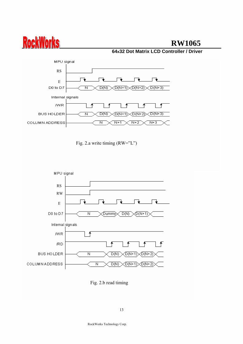
RW1065 64x32 Dot Matrix LCD Controller Driver
RockWorks Technology Corp
13
E
Fig 2b read timing
E
RW
Fig 2a write timing (RW=rdquoLrdquo)
RS
RS
RW1065 64x32 Dot Matrix LCD Controller Driver
RockWorks Technology Corp
14
Display Data RAM The display data RAM is a RAM that stores the dot data for the display It has a 64 (8 page x 8 bit) x 64 bit structure It is possible to access the desired bit by specifying the page address and the column addressBecause as is shown in Figure 3 the D7 to D0 display data from the MPU corresponds to the liquid crystal display common direction there are few constraints at the time of display data transfer when multiple RW1065 series chips are used
thus and display structures can be created easily and with a high degree of freedom Moreover reading from and writing to the display RAM from the MPU side is performed through the IO buffer which is an independent operation from signal reading for the liquid crystal driver Consequently even if the display data RAM is accessed asynchronously during liquid crystal display it will not cause adverse effects on the display (such as flickering)
0
1
0
0
1
1
0
0
1
0
1
0
0
1
0
1
0
0
1
0
0
0
0
0
0
D0
D1
D2
D3
D4
-
Display data RAM Liquid crystal display
COM0
COM1
COM2
COM3
COM4
-
Figure3
The Page Address Circuit As shown in Figure 4 page address of the display data RAM is specified through the Page Address Set Command The page address must be specified again when changing pages to perform access
The Column Address As is shown in Table 4 the display data RAM column address is specified by the Column Address Set command The specified column address is incremented (+1) with each display data readwrite command This allows the MPU display data to be accessed continuously Moreover the increment of column addresses stops with 3FH Because the column address is independent of the page address when moving for example from page 0 column 3FH to page 1
column 00H it is necessary to respecify both the page address and the column address Furthermore as is shown in Table 4 the ADC command (segment driver direction select command) can be used to reverse the relationship between the display data RAM column address and the segment output Because of this the constraints on the IC layout when the LCD module is assembled can be minimized
Table 4 SEG Output
ADC set SEG0 SEG 63
ADC(D0)=0 0 rarr Column Address rarr 63 ADC(D0)=1 63 larr Column Address larr 0
RW1065 64x32 Dot Matrix LCD Controller Driver
RockWorks Technology Corp
15
Figure 4
Page Address D3 D2 D1 D0
DataSE
G0
SEG
1
SEG
2
SEG
3
SEG
4
SEG
5
SEG
6
SEG
7
SEG
8
helliphelliphelliphellip
SEG
55
SEG
56
SEG
57
SEG
58
SEG
59
SEG
60
SEG
61
SEG
62
SEG
63 SEG
COM
D0 COM0
D1 COM1
D2 COM2
D3 COM3
D4 COM4
D5 COM5
D6 COM6
0 0 0 0
D7
Page 0
COM7
D0 COM8
D1 COM9
D2 COM10
D3 COM11
D4 COM12
D5 COM13
D6 COM14
0 0 0 1
D7
Page 1
COM15
D0 COM16
D1 COM17
D2 COM18
D3 COM19
D4 COM20
D5 COM21
D6 COM22
0 0 1 0
D7
Page 2
COM23
D0 COM24
D1 COM25
D2 COM26
D3 COM27
D4 COM28
D5 COM29
D6 COM30
0 0 1 1
D7
Page 3
COM31
ADC=0 00
01
02
03
04
05
06
07
08
helliphelliphelliphellip 55
56
57
58
59
60
61
62
63
COLUMN ADC=1 63
62
61
60
59
58
57
56
55
helliphelliphelliphellip 08
07
06
05
04
03
02
01
00
RW1065 64x32 Dot Matrix LCD Controller Driver
RockWorks Technology Corp
16
Common Timing Generator Circuit Display Data Latch Circuit Generates common timing signals and FR frame signals from the CL basic clock The 132 or 164 duty (for RW1065) can be selected by the Duty Select command The 132 and 164 duties are provided by two chips consisting of the master and slave chips in the common multi-chip mode
This latch stores one line of display data for use by the LCD driver interface circuitry The output of this latch is controlled by the Display ONOFF
132 duty
164 duty
SHL=0
SHL=1
SHL=0
SHL=1
RW1065 64x32 Dot Matrix LCD Controller Driver
RockWorks Technology Corp
17
Display Timing Generator Circuit
The display timing generator circuit generates the timing signal to the line address circuit and the display data latch circuit using the display clock The display data is latched into the display data latch circuit synchronized with the display clock and is output to the data driver output terminal Reading to the display data liquid crystal driver circuits is completely independent of accesses to the display data RAM by the MPU Consequently even if the display data
RAM is accessed asynchronously during liquid crystal display there is absolutely no adverse effect (such asflickering) on the display Moreover the display timing generator circuit generates the common timing and the liquid crystal alternating current signal (FR) from the display clock It generates a drive wave form using a 2 frame alternating current drive method as is shown in Figure 5 for the liquid crystal drive circuit
Two-frame alternating current drive waveform
Figure 5
When multiple RW1065 Series chips are used the slave chip must be supplied the display timing signals(FR CL) from the master chip
Table 5 shows the status of the FR and CL signals
Table 5 Operating Mode FR CL
Master (MS = ldquoHrdquo) The internal oscillator circuit is enabled (CLS = ldquoHrdquo) The internal oscillator circuit is disabled (CLS = ldquoLrdquo)
Output Output
Output Input
Slave (MS = ldquoLrdquo) The internal oscillator circuit is enabled (CLS = ldquoHrdquo) The internal oscillator circuit is disabled (CLS = ldquoLrdquo)
Input Input
Input Input
RW1065 64x32 Dot Matrix LCD Controller Driver
RockWorks Technology Corp
18
The Liquid Crystal Driver Circuits
These are a 64-channel (RW1065) that generate four voltage levels for driving the liquid crystal The combination of the display data the COM scan signal and the FR signal
produces the liquid crystal drive voltage output Figure 6 shows examples of the SEG and COM output waveform
Figure 6
RW1065 64x32 Dot Matrix LCD Controller Driver
RockWorks Technology Corp
19
The Power Supply Circuit
The power supply circuits are low-power consumption power supply circuits that generate the voltage levels required for the liquid crystal drivers They comprise Booster circuits and voltage follower circuits They are only enabled in master operation The power supply circuits can turn on automatically after power on
Consequently it is possible to make an external power supply and the internal power supply function somewhat in parallel
The Liquid Crystal Voltage Generator Circuit The V0 voltage is produced by a resistive voltage divider outside the IC through VRAB pin and can be produced at the V1 V2 V3 and V4 voltage levels required for liquid crystal driving Moreover when the voltage follower changes the impedance it provides V1 V2 V3 and V4 to the liquid crystal drive circuit 15 bias or 16 bias or 18 bias or 19 bias for RW1065 can be selected by BS0 and BS1 pins V0-Vss maximum voltage is 15V Vout-Vss maximum voltage is 17V If VDD lt 35V it can use the Booster circuit 2x3x4xThe booster voltage can follow the spec condition (Vout-Vss ≦ 17V max voltage) if VDD gt35V only use the 2X3X booster circuit that can ensure the V0-Vss voltage ≦ 15V If use the VDD voltage 5V and 4X booster itrsquos over the spec operation condition To turn on built-in power (boosterfollower) must waiting 200mS to display on for boosterfollower stable Therefore power off must follower ldquopower off sequencerdquo too
Power on Display off
Power off
Power off sequence
Wait time gt200mS
Display on
Power on sequence
RW1065 64x32 Dot Matrix LCD Controller Driver
RockWorks Technology Corp
20
The Reset Circuit
When the RTP input comes to the ldquoLrdquo level these LSIs return to the default state Their default states are as follows 1 Display OFF 2 Display all point on is select to normal 3 Display normalreverse is select to normal 4 164 duty is selected 5 Read modify write OFF 6 Column address set to Address 0 7 Page address set to Page 0 8 Start line set to first line 9 Frame frequency set to default 10 Power save mode released 11 Ext set to ldquo0rdquo When the power is turned on the IC internal state becomes unstable and it is necessary to initialize it using the RSTP terminal After the initialization each input terminal should be controlled normally While RSTP is ldquoLrdquo the oscillator works but the display timing generator stops and the CL FR terminals are fixed to ldquoHrdquo The terminals D0 to D7 are not affected
RW1065 64x32 Dot Matrix LCD Controller Driver
RockWorks Technology Corp
21
TABLE OF RW1065 INSTRUCTIONS
Instruction code Instruction RS RW DB7 DB6 DB5 DB4 DB3 DB2 DB1 DB0 Description
EXT=0 or 1
MODE SET 0 0 0 0 0 0 1 1 0 EXT Set EXT mode
Instruction code Instruction RS RW DB7 DB6 DB5 DB4 DB3 DB2 DB1 DB0 Description
EXT=0 Display ONOFF 0 0 0 0 1 1 1 1 1 D D=0Display OFF
D=1Display ONSet page address 0 0 1 0 1 1 1 P2 P1 P0 Set page address
Set column address 0 0 0 1 Y5 Y4 Y3 Y2 Y1 Y0 Set column
address MSB
Read Status 0 1 BUSY 0 ON OFF RESET 0 0 0 0 Read register
status Write display
data 1 0 Write data Write data into DDRAM
Read display data 1 1 Read data Read data from
DDRAM Set initial
display line register
0 0 1 1 S5 S4 S3 S2 S1 S0 Specify the initial
display line to realize vertical scrolling
Instruction code Instruction RS RW DB7 DB6 DB5 DB4 DB3 DB2 DB1 DB0 Description
EXT=1
NOP 0 0 0 0 0 0 0 0 0 0 no operation
Set modiy-read 0 0 0 0 0 0 1 0 0 0 Set modiy-read
mode
END 0 0 0 0 0 0 1 1 1 0 release modiy-read mode
Set power save mode 0 0 0 0 0 0 0 0 1 PSAVE P=0 normal mode
P=1 sleep mode
0 0 0 0 0 1 0 1 Display
COMMAND (double
command)
0 0 FRSEL
0 0 0 0 REV ALLON DUTY
DUTY=1 64 duty DUTY=0 32 duty ALLON=1display all on ALLON=0display
normal REV=1display reverse REV=0display normal FRSEL=1FR frequency double default FRSEL=0FR frequency default
RW1065 64x32 Dot Matrix LCD Controller Driver
RockWorks Technology Corp
22
Command Description
See the Table of RW1065 instructions The RW1065 series identifies a data bus using a combination of RS E and RW signals As the MPU translates a command in the internal timing only (independent from the external clock) its speed is very high The busy check is usually not required
Display ONOFF
EXT RS RW D7 D6 D5 D4 D3 D2 D1 D0
0 0 0 0 0 1 1 1 1 1 D
This command turns the display on and off D=1 Display ON D=0 Display OFF(default)
Set page Address This command specifies the page address that corresponds to the low address of the display data RAM when it is accessed by the MPU Any bit of the display data RAM can be accessed when its page address and column address are specified The display status is not changed even when the page address is changed
EXT RS RW D7 D6 D5 D4 D3 D2 D1 D0
0 0 0 1 0 1 1 1 A2 A1 A0
This command loads the page address register
A2 A1 A0 Page
0 0 0 0 (default)
0 0 1 1 0 1 0 2 0 1 1 3 1 0 0 4 1 0 1 5 1 1 0 6 1 1 1 7
Page mapping see Figure 4
RW1065 64x32 Dot Matrix LCD Controller Driver
RockWorks Technology Corp
23
Set Column Address This command specifies a column address of the display data RAM When the display data RAM is accessed by the MPU continuously the column address is incremented by I each time it is accessed from the set address Therefore the MPU can access to data continuously The column address stops to be incremented at address 63 and the page address is not changed continuously
EXT RS RW D7 D6 D5 D4 D3 D2 D1 D0
0 0 0 0 1 A5 A4 A3 A2 A1 A0
A5 A4 A3 A2 A1 A0 Column Address0 0 0 0 0 0 0(default) 0 0 0 0 0 1 1
1 1 1 1 1 1 63
Read Status
EXT RS RW D7 D6 D5 D4 D3 D2 D1 D0
0 0 1 BUSY 0 ON OFF RESET 0 0 0 0
The BUSY Flag bit indicates that RW 1065 is operating or no operating
BUSY=1 Operation BUSY=0 Ready
The ONOFF bit indicates the current status of the display It is the inverse of the polarity of the display ONOFF command ONOFF=1 Display OFF ONOFF=0 Display ON The RESET bit indicates whether the driver is executing a hardware or software reset or if it is in normal operating mode RESET=1 Currently executing reset command RESET=0 Normal operation
RW1065 64x32 Dot Matrix LCD Controller Driver
RockWorks Technology Corp
24
Write Display Data
EXT RS RW D7 D6 D5 D4 D3 D2 D1 D0
0 1 0 Write data
Writes 8-bits of data into the display data RAM at a location specified by the contents of the column address and page address registers and then increments the column address register by one
Read Display Data
EXT RS RW D7 D6 D5 D4 D3 D2 D1 D0
0 1 1 Read data
Reads 8-bits of data from the data IO latch updates the contents of the IO latch with display data from the display data RAM location specified by the contents of the column address and page address registers and then increments the column address register After loading a new address into the column address register one dummy read is required before valid data is obtained
Set initial display line register
EXT RS RW D7 D6 D5 D4 D3 D2 D1 D0
0 0 0 1 1 S5 S4 S3 S2 S1 S0
Loads the RAM line address of the initial display line COM 0 into the initial display line register The RAM display data becomes the top line of the LCD screen It is followed by the higher number lines in ascending order corresponding to the duty cycle The screen can be scrolled using this command by incrementing the line address(default value=rdquo00Hrdquo)
RW1065 64x32 Dot Matrix LCD Controller Driver
RockWorks Technology Corp
25
Read-Modify-Write
EXT RS RW D7 D6 D5 D4 D3 D2 D1 D0
1 0 0 0 0 0 0 1 0 0 0
This command defeats column address register auto-increment after data reads The current contents of the column Address register are saved The mode remains active until an End command is received When the End command is entered the column address is returned to the one used during input of Read-Modify-Write Command This function can reduce the load of MPU when data change is repeated as a specific display area Any command other than Data Read or Write can be used in the Read-Modify-Write mode However the Column Address Set command cannot be used
End
EXT RS RW D7 D6 D5 D4 D3 D2 D1 D0
1 0 0 0 0 0 0 1 1 1 0
This command cancels read-modify-write mode and restores the contents of the column address register to their value prior to the receipt of the Read-Modify-Write command
N N+1 N+2 N+3 N+m N
Read -modify-write mode set End
Returm
Column address
Set page address
Set column address
Read-modify-write
Dummy read
Read data
Write data
End
CompletedNo
Yes
RW1065 64x32 Dot Matrix LCD Controller Driver
RockWorks Technology Corp
26
Set power save mode
EXT RS RW D7 D6 D5 D4 D3 D2 D1 D0
1 0 0 0 0 0 0 0 0 1 PSAVE
When power save mode is entered thus greatly reducing power consumption In the power save mode the display data is saved as is the operating mode that was in effect before the power saver mode was initiated and the MPU is still able to access the display data RAM PSAVE=1 Sleep mode PSAVE=0 Normal mode Sleep mode This stops all operations in the LCD display system and as long as there are no accesses from the MPU the consumption current is reduced to a value near the static current The internal modes during sleep mode are as follows 1 The oscillator circuit and the LCD power supply circuit are halted 2 All liquid crystal drive circuits are halted and the segment and common drive outputs output a Vss level
Display command double command
EXT RS RW D7 D6 D5 D4 D3 D2 D1 D0
1 0 0 0 0 0 0 0 1 0 1
1 0 0 FRSEL 0 0 0 0 REV ALLON DUTY
Display NormalReverse set REV=1 Reverse REV=0 Normal(default) Display All Point ONOFF ALLON=1 All display points ON ALLON=0 Normal(default) Select Duty Duty=1 164 duty cycle(default) Duty=0 132 duty cycle FRAME FREQUENCY Select FRSEL=1 Double FRSEL=0 (default)
RW1065 64x32 Dot Matrix LCD Controller Driver
RockWorks Technology Corp
27
Hardware Pin Set
Select ADC by ADC Pin The pin selects the relationship between display data RAM column addresses and segment drivers ADC=1 SEG0larrcolumn address 3FHhellipinverted ADC=0 SEG0larrcolumn address 00Hhellipnormal(default) This command is provided to reduce restrictions on the placement of driver ICs and routing of traces during printed circuit Board design See Figure 4 for a table of segments and column addresses for the two values of D
Select SHL by SHL Pin The pin selects the com output scan direction SHL=1 Reverse directioncom63rarrcom0 SHL=0 Normal com0rarrcom63 Both master and slave should set identical SHL value
Select LCD Bias by BS0 BS1 Pin
BS1 BS0 Bias 0 0 15 bias 0 1 16 bias 1 0 18 bias 1 1 19 bias
RW1065 64x32 Dot Matrix LCD Controller Driver
RockWorks Technology Corp
28
When an External Resistance is Used The liquid crystal power supply voltage V0 is set by adding resistors Rarsquo and Rbrsquo between VDD and VR and between VR and V0 respectively
RW1065
RW1065 64x32 Dot Matrix LCD Controller Driver
RockWorks Technology Corp
29
The set voltage circuits
Using the step-up voltage circuits equipped within the RW1065 chips it is possible to produce a 2X 3X 4X step-up voltage levels 2X step-up
To produce voltage level in the positive direction at the Vout terminal that is 2 times the voltage difference between VSS and VDD2 Please configure set voltage circuits like this Place a 1uF~22uF capacitor between CAP1N and CAP1P Place a 1uF~22uF capacitor between VSS and VOUT Short CAP2P CAP3P and VOUT Leave CAP2N open 3X step-up
To produce voltage level in the positive direction at the Vout terminal that is 3 times the voltage difference between VSS and VDD2 Please configure set voltage circuits like this Place a 1uF~22uF capacitor between CAP1N and CAP1P Place a 1uF~22uF capacitor between VSS and VOUT Place a 1uF~22uF capacitor and 100 ohms resistor between CAP2N and CAP2P Short CAP3P and Vout 4X step-up
To produce voltage level in the positive direction at the Vout terminal that is 4 times the voltage difference between VSS and VDD2 Please configure set voltage circuits like this Place a 1uF~22uF capacitor between CAP1N and CAP1P Place a 1uF~22uF capacitor between VSS and VOUT Place a 1uF~22uF capacitor and 100 ohms resistor between CAP2N and CAP2P Place a 1uF~22uF capacitor and 100 ohms resistor between CAP1N and CAP3P
RW1065 64x32 Dot Matrix LCD Controller Driver
RockWorks Technology Corp
30
ABSOLUTE MAXIMUM RATINGS Characteristics Symbol Value Unit
Power supply voltage VDD -03 to +70 V
LCD driver voltage Vout 0 to +17 V
Input voltage VIN -03 to VDD+03 V
Operating temperature TA -40 to +85
Storage temperature TSTO -55 to +125
DC CHARACTERISTICS
Rating Item Symbol Condition Min Typ Max Unit ApplicablePin
Operating Voltage VDD - 27 30 55 V VDD1
Step up output voltage Vout (Relative to VDD) 0 - 17 V Vout
Voltage follower circuit operating Voltage V0 (Relative to VDD) 0 - 15 V V0
V0 accuracy V0 - 0 - 15 V0
High-level Input Voltage Low-level Input Voltage
VIHC VILC - 07 VDD
Vss - VDD 09 V 2
High-level Output Voltage Low-level Output Voltage
VOHC VOLC
IOH = ndash05 mA IOL = 05 mA
08VDD Vss - VDD
02 VDD V 3
Input leakage current ILI VIN = VDD or VSS -1 - 2 uA 4
Output leakage current ILO - -1 1 uA 5
Liquid Crystal Driver ON Resistance RON
Ta= 25degC(Relative To VDD)
V0 =15 V - 16 20 KΩ SEGn COMn 6
Internal Oscillator fOSC 2286 254 2794 Oscillator
Frequency External Input RECOMMAND fCL
Ta = 25degC 132Duty 2286 254 2794
kHz CL
Internal Oscillator fOSC 45 5 55 Oscillator
Frequency External Input RECOMMAND fCL
Ta = 25degC 164Duty 45 5 55
kHz CL
bullDynamic Consumption Current During Display with the Internal Power Supply OFF Current consumed by total ICs when an external power supply is used
Unless otherwise specified Vss=0V VDD=30V
RW1065 64x32 Dot Matrix LCD Controller Driver
RockWorks Technology Corp
31
Display Pattern OFF
Ta = 25degC Vout=17V Rating Item Symbol Condition Min Typ Max Unit Notes
VDD=30 V V0-Vss=8V - 10 15 RW1065 IDD VDD=50 V V0-Vss=8V - 35 45
microA 7
Display Pattern Checker
Ta = 25degC Vout=17V Rating Item Symbol Condition Min Typ Max Unit Notes
VDD=30 V V0-Vss=8V - 15 20 RW1065 IDD VDD=50 V V0-Vss=8V - 40 50
microA 7
Display Pattern OFF
Ta = 25degC Vout=17V Rating Item Symbol Condition Min Typ Max Unit Notes
VDD=30 V V0-Vss=8V - 15 20 RW1065 IDD VDD=50 V V0-Vss=8V - 40 50
microA 7
Display pattern Checker
Ta = 25degC Vout=17V Rating Item Symbol Condition Min Typ Max Unit Notes
VDD=30 V V0-Vss=8V - 65 80 RW1065 IDD VDD=50 V V0-Vss=8V - 130 150
microA 7
bull Consumption Current at Time of Power Saver Mode VSS = 0 V VDD = 30 V plusmn 10
Rating Item Symbol Condition Min Typ Max Unit Notes
Sleep mode IDD - - 5 10 microA -
References for items market with 1 While a broad range of operating voltages is guaranteed performance cannot be guaranteed if there are sudden fluctuations to the
voltage while the MPU is being accessed 2 The RS D0 to D5 D6 D7 E RW CS1BP CS2P CLS CL FR MS and RST
― terminals
3 The D0 to D7 FR and CL terminals 4 The RS E RW CS1BP CS2P CLS MS and RST
― terminals
5 Applies when the D0 to D5 D6 D7 CL and FR terminals are in a high impedance state 6 These are the resistance values for when a 01 V voltage is applied between the output terminals SEGn or COMn and
the various power supply terminals (V1 V2 V3 and V4) These are specified for the operating voltage (3) range RON = 01 V ∆I (Where ∆I is the current that flows when 01 V is applied while the power supply is ON)
7 It indicates the current consumed on ICs alone when the internal oscillator circuit and display are turned on Does not include the current due to the LCD panel capacity and wiring capacity Applicable only when there is no access from the MPU
RW1065 64x32 Dot Matrix LCD Controller Driver
RockWorks Technology Corp
32
TIMING CHARACTERISTICS
68 Interface
(Ta=-40 to 85 degC) VDD=27 to 45V
Rating VDD=45 to 55V
Rating Item Signal Symbol ConditionMin Max Min Max
Units
Address hold time RS tAH6 0 mdash 0 mdash Address setup time RS tAW6
mdash 0 mdash 0 mdash
ns
System cycle time RS tCYC6 mdash 900 mdash 800 mdash ns Data setup time D0 to D7 tDS6 100 mdash 100 mdash Data hold time D0 to D7 tDH6
mdash 0 mdash 0 mdash
ns
Access time D0 to D7 tACC6 mdash 350 mdash 250
Output disable time D0 to D7 tOH6 CL = 100 pF
mdash 300 mdash 200 ns
Read tEWHR 360 mdash 300 mdash Enable H pulse time
WriteE
tEWHW mdash
360 mdash 300 mdash ns
Read tEWLR 450 mdash 400 mdash Enable L pulse time
WriteE
tEWLW mdash
450 mdash 400 mdash ns
1 All timing is specified using 20 and 80 of VDD as the reference 2 tEWLW and tEWLR are specified as the overlap between CS1BP being ldquoLrdquo (CS2P = ldquoHrdquo) and E
RW1065 64x32 Dot Matrix LCD Controller Driver
RockWorks Technology Corp
33
Reset Timing
Rating Item Signal Symbol Condition
Min Typ Max Units
Reset time mdash tR mdash mdash - 2 micros
Reset ldquoLrdquo pulse width RST tRW mdash 2 - mdash micros
1 When double chip was be used then the duty set command must be set between the tR
RW1065 64x32 Dot Matrix LCD Controller Driver
RockWorks Technology Corp
34
IO PAD CONFIGURATION
RW1065 64x32 Dot Matrix LCD Controller Driver
RockWorks Technology Corp
35
THE MPU INTERFACE (REFERENCE EXAMPLES) The RW1065 Series can be connected to 6800 Series MPUs The display area can be enlarged by using multiple RW1065 Series chips When this is done the chip select signal can be used to select the individual ICs to access
6800 Series MPUs
RW
106
5
RW1065 64x32 Dot Matrix LCD Controller Driver
RockWorks Technology Corp
36
When using external multi-level power supply for LCD driving (REFERENCE EXAMPLE)
Using a resistor divider can provide RW1065 external multi-level power supply for LCD driving
The circuit below shows a resistor divider network which can bias V0 V1 V2 V3 and V4 externally
RW1065 64x32 Dot Matrix LCD Controller Driver
RockWorks Technology Corp
37
bullWhen V0 V1 V2 V3 and V4 are biased by external power supply analog section of RW1065 should be turn off by software during LCD initialization The example in below shows the sequence to turn off analog section when external bias is used Begin of LCD initialization 1 Reset RW1065 2 SET EXT=1 (mode instruction)
RS RW DB7 DB6 DB5 DB4 DB3 DB2 DB1 DB00 0 0 0 0 0 1 1 0 1
3 SET Display Command (double command)
RS RW DB7 DB6 DB5 DB4 DB3 DB2 DB1 DB00 0 0 0 0 0 0 1 0 1 0 0 0 0 1 1 0 0 0 1
4 SET EXT=1 (mode instruction)
RS RW DB7 DB6 DB5 DB4 DB3 DB2 DB1 DB00 0 0 0 0 0 1 1 0 0
End of LCD initialization
bullBecause pins can not set LCD bias when external power supplies are used for LCD driving the bias can be set by an appropriate configuration for a resistor voltage divider networks The example is shown below
VSS
R
R
NR
R
R
RV1
RV2
RV3
RV4
V0
Bias Network Circuit Concept 15 Bias N=1 total = 5R 16 Bias N=2 total =6R 18 Bias N=4 total =8R 19 Bias N=5 total = 9R
RW1065 64x32 Dot Matrix LCD Controller Driver
RockWorks Technology Corp
38
Single chip solution for RW1065 application (REFERENCE EXAMPLE)
For a 64x32 application the duty cycle of LCD panel is 164 and the display duty of RW1065 should be set to 164 The display duty cycle can be selected by the DUTY bit in display command The diagram for 64x32 application is shown below
64 SEGx32COM LCD Panel
164 duty cycle
RW1065 DUTY=1
COM1~33
SEG1~65
RW1065 64x32 Dot Matrix LCD Controller Driver
RockWorks Technology Corp
39
Using an adjustable resistor on the main board to adjust the contrast of liquid crystal display (REFERENCE EXAMPLE)
The schematic shows an adjustable resistor on main board that can adjust voltage level of V0
RW1065 64x32 Dot Matrix LCD Controller Driver
RockWorks Technology Corp
40
Package information (Please pay close attention to the information in this section Do not hesitate to consult with our sale representative if you have any question or concern)
In order to make better bonding yield for RW1065 please follow the tips and recommendations in this section In this section few tips about COB footprint style PCB layout and wire bonding will be discussed
The drawing in below shows the PCB footprint style which we recommend for RW1065 Pads array in
curve shape is easier for Al wire bonding Besides that a real size COB footprint for RW1065 is also shown in below RW1065 COB footprint is also available in powerpcb or protel format for design reference purpose
The ratio is 11
RW1065 64x32 Dot Matrix LCD Controller Driver
RockWorks Technology Corp
41
During COB footprint design there have some tips about footprint that the PCB designer should know The angle between bonding wire and vertical line should less than 45 Otherwise the wire shorts would become very easy to happen at fours corners of the chip
The angle between bonding wire and vertical line could be reduced by expanding the distance between pads array and the chip In addition reducing length in horizon direction of pads array could minimize the angle between bonding wire and vertical line The picture in below will help to illustrate this concept From the experiences COB footprint style affects the bonding yield
Bad Wires are too close to each other
The angle between bonding wire and vertical line is greater than 45
The angle between bonding wire and vertical line is less than 45
Wires are not too close to each other
Reducing length in horizon direction of pads array could minimize the angle between bonding wire and vertical line
The angle between bonding wire and vertical line could be reduced by expanding the distance between pads array and the chip
RW1065 64x32 Dot Matrix LCD Controller Driver
RockWorks Technology Corp
42
If the gap between pads of COB footprint is filled with solder mask coating it is difficult to bond Al wire to
the pads The top solder masks layer that overlap COB footprint area should be removed
Please use 1 mils diameter Al wire for RW1065 wire bonding
1 2 3 4 5 6
A
B
C
D
654321
D
C
B
A
Title
Number RevisionSize
C
Date 29-Aug-2007 Sheet of File D公司資料99seMyDesignddb Drawn By
RW1065
COM131
COM142
COM153
COM164
COM175
COM186
COM197
COM208
COM219
COM2210
COM2311
COM2412
COM2513
COM2614
COM2715
COM2816
COM2917
COM3018
COM3119
SEG
6320
SEG
6221
SEG
6122
SEG
6023
SEG
5924
SEG
5825
SEG
5726
SEG
5627
SEG
5528
SEG
5429
SEG
5330
SEG
5231
SEG
5132
SEG
5033
SEG
4934
SEG
4835
SEG
4736
SEG
4637
SEG
4538
SEG
4439
SEG
4340
SEG
4241
SEG
4142
SEG
4043
SEG
3944
SEG
3845
SEG
3746
SEG
3647
SEG
3548
SEG
3449
SEG
3350
SEG
3251
SEG
3152
SEG
3053
SEG
2954
SEG
2855
SEG
2756
SEG
2657
SEG
2558
SEG
2459
SEG
2360
SEG
2261
SEG
2162
SEG
2063
SEG
1964
SEG
1865
SEG
1766
SEG
1667
SEG
1568
SEG
1469
SEG13 70SEG12 71SEG11 72SEG10 73SEG9 74SEG8 75SEG7 76SEG6 77SEG5 78SEG4 79SEG3 80SEG2 81SEG1 82SEG0 83ADCP 84CLL 85
VSS
86D
087
D1
88D
289
D3
90D
491
D5
92D
693
D7
94C
S1B
P95
CS2
P96
ERD
P97
AO
P(R
S)98
RW
RP
99V
DD
100
RST
P10
1C
LSP
102
FRR
103
MSP
104
BS1
P10
5B
S0P
106
SHLP
107
VD
D2
108
CA
P2N
109
CA
P2P
110
CA
P1P
111
CA
P1N
112
CA
P3P
113
VO
UT
114
V0
115
VR
AB
116
V3
117
V2
118
V4
119
V1
120
CO
M0
121
CO
M1
122
CO
M2
123
CO
M3
124
CO
M4
125
CO
M5
126
CO
M6
127
CO
M7
128
CO
M8
129
CO
M9
130
CO
M10
131
CO
M11
132
CO
M12
133
4897x1902 um
IC1
RW1065
C9CAPR4
100R0603
R30R0603
C8
CAP
C7
CAP
R2
100R0603
R1
0R0603C6 22uf
R50R
R6300R
R7RES1
R8NC R9
100R0603
VDD
R10
NC
R11
100R0603
R12
100R0603
R13
NC
R14
100R0603
R15
NC
VDD
D0
D1
D2
D3
D4
D5
D6
D7
DB[07]
VDDC5
01uf0603
VD
D
CS2
P
123456789
1011121314151617181920
J1
CON20
C1201uf0603
R3951K0603
VDD
CAP Value1UF~22UF
2XPut C6C8 Short R1R3Open R2R4C7C93XPut C6C8C9 R4Short R1Open R2R3C74XOpen R1R3
BS0 BS1 Bias0 0
0 1
1 0
11
15 bias
16 bias
18 bias
19 bias
ADC=0 SEG0lt~column address 00Hnormal(default) ADC=1 SEG0lt~column address 3FHinverted
SHL=0 Normal COM0~gtCOM63(default)SHL=1 Reverse direction COM63~gtCOM0
R16100R0603
LCD PANEL 64X32RockWorks
RW1065 64X32
COM0-31 SEG0-63SHL=0 ADC=0
SHL=1COM31-0
ADC=1SEG63-0
if use single chip for 32 command displaythe display command must select 164 dutyDisplay panel must select 164 duty type
VO
UT
C3P
C1N
C1P
C2P
C2N
VDD2
ADC
SHL
BS0
BS1
CLLADC
V1
V2
V3
V4
VR
AB
V0
VO
UT
C3P
C1N
C1P
C2P
C2N
VD
D2
SHL
BS0
BS1
FRR
RST
P
RW
RS
E CS1
B
CS1
V0RSRWED0D1D2D3D4D5D6D7
RSTPAK
C4
22uf
RBRES1
RA1RES1
C2
22uf
C1
22uf
C3
22uf
C0
22uf
R20
100k0603
R21
100k0603
R17
200K0603
V1
V2
V3
V4 VRAB
V0
V0
OPTION
B
R18
300R0603
RA2RES1
VADJ
R19100R
R23 RES1R22 0R
R24
RES1
R25
0R
VDD
CS1BP
CS2P
CS1
CS1
R26
22R0603
R27
22R0603
C1047uf
C11
01uf
VSS_INVDD_IN
D1DIODE
FGND
鐵框地
VSS
VDD
R28 10RR29 10RR30 10RR31 10RR32 10RR33 10RR34 10RR35 10RR36 10RR37 10RR38 10R
VADJ
1 2 3 4 5 6
A
B
C
D
654321
D
C
B
A
Title
Number RevisionSize
C
Date 29-Aug-2007 Sheet of File D公司資料99seMyDesignddb Drawn By
RW1065
COM131
COM142
COM153
COM164
COM175
COM186
COM197
COM208
COM219
COM2210
COM2311
COM2412
COM2513
COM2614
COM2715
COM2816
COM2917
COM3018
COM3119
SEG
6320
SEG
6221
SEG
6122
SEG
6023
SEG
5924
SEG
5825
SEG
5726
SEG
5627
SEG
5528
SEG
5429
SEG
5330
SEG
5231
SEG
5132
SEG
5033
SEG
4934
SEG
4835
SEG
4736
SEG
4637
SEG
4538
SEG
4439
SEG
4340
SEG
4241
SEG
4142
SEG
4043
SEG
3944
SEG
3845
SEG
3746
SEG
3647
SEG
3548
SEG
3449
SEG
3350
SEG
3251
SEG
3152
SEG
3053
SEG
2954
SEG
2855
SEG
2756
SEG
2657
SEG
2558
SEG
2459
SEG
2360
SEG
2261
SEG
2162
SEG
2063
SEG
1964
SEG
1865
SEG
1766
SEG
1667
SEG
1568
SEG
1469
SEG13 70SEG12 71SEG11 72SEG10 73SEG9 74SEG8 75SEG7 76SEG6 77SEG5 78SEG4 79SEG3 80SEG2 81SEG1 82SEG0 83ADCP 84CLL 85
VSS
86D
087
D1
88D
289
D3
90D
491
D5
92D
693
D7
94C
S1B
P95
CS2
P96
ERD
P97
AO
P(R
S)98
RW
RP
99V
DD
100
RST
P10
1C
LSP
102
FRR
103
MSP
104
BS1
P10
5B
S0P
106
SHLP
107
VD
D2
108
CA
P2N
109
CA
P2P
110
CA
P1P
111
CA
P1N
112
CA
P3P
113
VO
UT
114
V0
115
VR
AB
116
V3
117
V2
118
V4
119
V1
120
CO
M0
121
CO
M1
122
CO
M2
123
CO
M3
124
CO
M4
125
CO
M5
126
CO
M6
127
CO
M7
128
CO
M8
129
CO
M9
130
CO
M10
131
CO
M11
132
CO
M12
133
4897x1902 um
IC1
RW1065 Master
RW1065
COM131
COM142
COM153
COM164
COM175
COM186
COM197
COM208
COM219
COM2210
COM2311
COM2412
COM2513
COM2614
COM2715
COM2816
COM2917
COM3018
COM3119
SEG
6320
SEG
6221
SEG
6122
SEG
6023
SEG
5924
SEG
5825
SEG
5726
SEG
5627
SEG
5528
SEG
5429
SEG
5330
SEG
5231
SEG
5132
SEG
5033
SEG
4934
SEG
4835
SEG
4736
SEG
4637
SEG
4538
SEG
4439
SEG
4340
SEG
4241
SEG
4142
SEG
4043
SEG
3944
SEG
3845
SEG
3746
SEG
3647
SEG
3548
SEG
3449
SEG
3350
SEG
3251
SEG
3152
SEG
3053
SEG
2954
SEG
2855
SEG
2756
SEG
2657
SEG
2558
SEG
2459
SEG
2360
SEG
2261
SEG
2162
SEG
2063
SEG
1964
SEG
1865
SEG
1766
SEG
1667
SEG
1568
SEG
1469
SEG13 70SEG12 71SEG11 72SEG10 73SEG9 74SEG8 75SEG7 76SEG6 77SEG5 78SEG4 79SEG3 80SEG2 81SEG1 82SEG0 83ADCP 84CLL 85
VSS
86D
087
D1
88D
289
D3
90D
491
D5
92D
693
D7
94C
S1B
P95
CS2
P96
ERD
P97
AO
P(R
S)98
RW
RP
99V
DD
100
RST
P10
1C
LSP
102
FRR
103
MSP
104
BS1
P10
5B
S0P
106
SHLP
107
VD
D2
108
CA
P2N
109
CA
P2P
110
CA
P1P
111
CA
P1N
112
CA
P3P
113
VO
UT
114
V0
115
VR
AB
116
V3
117
V2
118
V4
119
V1
120
CO
M0
121
CO
M1
122
CO
M2
123
CO
M3
124
CO
M4
125
CO
M5
126
CO
M6
127
CO
M7
128
CO
M8
129
CO
M9
130
CO
M10
131
CO
M11
132
CO
M12
133
4897x1902 um
IC2
RW1065 Slave
C4
22uf
RBRES1
RA1RES1
C2
22uf
C1
22uf
C3
22uf
C0
22ufC9CAPR4
100R0603
R30R0603
C8
CAP
C7
CAP
R2
100R0603
R1
0R0603C6 22uf
R50R0603
R6300R0603
R7RES1
R8NC R9
100R0603
VDD
R10
NC
R11
100R0603
R12
NC
R13
100R0603
R14
100R0603
R15
NC
R16
100R0603
R17
NC
VDD
D0
D1
D2
D3
D4
D5
D6
D7
D0
D1
D2
D3
D4
D5
D6
D7
DB[07] DB[07]
VDDC10
01uf0603
VD
D
IC1_
CS2
P
VDD
IC2_
CS2
P
VD
D
C11
01uf0603
VSS
VSS
LCD PANEL 128X64
Master COM0-31 Slave COM32-63
Master SEG0-63 Slave SEG64-127
123456789
1011121314151617181920
J1
CON20
Master Slave
CAP Value1UF~22UF
2XPut C6C8 Short R1R3Open R2R4C7C93XPut C6C8C9 R4Short R1Open R2R3C74XOpen R1R3
RockWorksRW1065 128x64
BS0 BS1 Bias0 0
0 1
1 0
11
15 bias
16 bias
18 bias
19 bias
ADC=0 SEG0lt~column address 00Hnormal(default) ADC=1 SEG0lt~column address 3FHinverted
SHL=0 Normal COM0~gtCOM63(default)SHL=1 Reverse direction COM63~gtCOM0Both Master and Slave should set identical SHL value
SHL=0 SHL=0
ADC=0 ADC=0
Slave COM31-0
Slave SEG127-64
SHL=1
ADC=1
SHL=1Master COM63-32
ADC=1Master SEG63-0
R18100R0603
R22
100k0603
R23
100k0603
C501uF0603
R4551K0603
VDD
R19
200K0603
ADC1
ADC2
SHL
BS0
BS1
VDD2
V1
V2
V3
V4 VRAB
V0
V0V
OU
T
C3P
C1N
C1P
C2P
C2N
V1
V2
V3
V4
VR
AB
V0
VO
UT
C3P
C1N
C1P
C2P
C2N
VD
D2
SHL
BS0
BS1
FRR
RST
P
RW
RS
E IC1_
CS1
BP
V1
V2
V3
V4
VR
AB
V0
VO
UT
VD
D2
SHL
BS0
BS1
FRR
RST
P
RW
RS
E IC2_
CS1
BP
CLLADC1
CLLADC2
RSTP
CS1CS2
V0RSRWED0D1D2D3D4D5D6D7
AK
OPTION
R20
300R0603
RA2RES1
VADJ
R21
100R
B
R25 RESR24 0R
R26 RES R27 0RVDD
IC1_CS1BP
IC1_CS2P
CS1
CS1
R28 0R R29 RES
R30 RES R31 0R
IC2_CS1BP
IC2_CS2P
CS2
CS2
R32
22R0603
R33
22R0603
C1001uf
C11
47uf
D1DIODE
FGND
鐵框地
VSS
VDD
R34 10RR35 10RR36 10RR37 10RR38 10RR39 10RR40 10RR41 10RR42 10RR43 10RR44 10R
VSS_INVDD_IN
VADJ
VDD
1 2 3 4 5 6 7 8
A
B
C
D
87654321
D
C
B
A
Title
Number RevisionSize
D
Date 29-Aug-2007 Sheet of File D公司資料 99seMyDesignddb Drawn By
C422uf
RBRES1
RA1RES1
C3
22uf
C2
22uf
C1
22uf
C0
22ufC9CAPR4
100R0603
R30R0603
C8
CAP
C7
CAP
R2
100R0603
R1
0R0603C6 22uf
R220R0603
R23300R0603
R24RES1
R39
NCR40
100 ohm0603
VDD
R41
NC
R42
100 ohm0603
R43
NC
R44
100 ohm0603
R45
NC
R46
100 ohm0603
R47
100 ohm0603
R48
NC
R49
100 ohm0603
R50
NC
VDDCAP Value1UF~22UF
2XPut C6C8 Short R1R3Open R2R4C7C93XPut C6C8C9 R4Short R1Open R2R3C74XOpen R1R3
BS0 BS1 Bias0 0
0 1
1 0
11
15 bias
16 bias
18 bias
19 bias
ADC=0 SEG0lt~column address 00Hnormal(default)
ADC=1 SEG0lt~column address 3FHinverted
SHL=0 Normal COM0~gtCOM63(default)SHL=1 Reverse direction COM63~gtCOM0Both Master and Slave should set identical SHL value
R7
100k0603
R8
100k0603
V1
V2
V3
V4
V0
VRAB
V0
R5
200K
VDD2
VO
UT
C3P
C1N
C1P
C2P
C2N
ADC1
ADC2
ADC3
SHL
BS0
BS1
CS1CS2CS3
V0RSRWED0D1D2D3D4D5D6D7
RSTP
R3851K0603
C5
01uF
VDD
OPTION
R6
300R0603R9100R
RA2RES1
VADJ
RW1065
COM131
COM142
COM153
COM164
COM175
COM186
COM197
COM208
COM219
COM2210
COM2311
COM2412
COM2513
COM2614
COM2715
COM2816
COM2917
COM3018
COM3119
SEG
6320
SEG
6221
SEG
6122
SEG
6023
SEG
5924
SEG
5825
SEG
5726
SEG
5627
SEG
5528
SEG
5429
SEG
5330
SEG
5231
SEG
5132
SEG
5033
SEG
4934
SEG
4835
SEG
4736
SEG
4637
SEG
4538
SEG
4439
SEG
4340
SEG
4241
SEG
4142
SEG
4043
SEG
3944
SEG
3845
SEG
3746
SEG
3647
SEG
3548
SEG
3449
SEG
3350
SEG
3251
SEG
3152
SEG
3053
SEG
2954
SEG
2855
SEG
2756
SEG
2657
SEG
2558
SEG
2459
SEG
2360
SEG
2261
SEG
2162
SEG
2063
SEG
1964
SEG
1865
SEG
1766
SEG
1667
SEG
1568
SEG
1469
SEG13 70SEG12 71SEG11 72SEG10 73SEG9 74SEG8 75SEG7 76SEG6 77SEG5 78SEG4 79SEG3 80SEG2 81SEG1 82SEG0 83ADCP 84CLL 85
VSS
86D
087
D1
88D
289
D3
90D
491
D5
92D
693
D7
94C
S1B
P95
CS2
P96
ERD
P97
AO
P(R
S)98
RW
RP
99V
DD
100
RST
P10
1C
LSP
102
FRR
103
MSP
104
BS1
P10
5B
S0P
106
SHLP
107
VD
D2
108
CA
P2N
109
CA
P2P
110
CA
P1P
111
CA
P1N
112
CA
P3P
113
VO
UT
114
V0
115
VR
AB
116
V3
117
V2
118
V4
119
V1
120
CO
M0
121
CO
M1
122
CO
M2
123
CO
M3
124
CO
M4
125
CO
M5
126
CO
M6
127
CO
M7
128
CO
M8
129
CO
M9
130
CO
M10
131
CO
M11
132
CO
M12
133
4897x1902 um
IC1
RW1065 Master
RW1065
COM131
COM142
COM153
COM164
COM175
COM186
COM197
COM208
COM219
COM2210
COM2311
COM2412
COM2513
COM2614
COM2715
COM2816
COM2917
COM3018
COM3119
SEG
6320
SEG
6221
SEG
6122
SEG
6023
SEG
5924
SEG
5825
SEG
5726
SEG
5627
SEG
5528
SEG
5429
SEG
5330
SEG
5231
SEG
5132
SEG
5033
SEG
4934
SEG
4835
SEG
4736
SEG
4637
SEG
4538
SEG
4439
SEG
4340
SEG
4241
SEG
4142
SEG
4043
SEG
3944
SEG
3845
SEG
3746
SEG
3647
SEG
3548
SEG
3449
SEG
3350
SEG
3251
SEG
3152
SEG
3053
SEG
2954
SEG
2855
SEG
2756
SEG
2657
SEG
2558
SEG
2459
SEG
2360
SEG
2261
SEG
2162
SEG
2063
SEG
1964
SEG
1865
SEG
1766
SEG
1667
SEG
1568
SEG
1469
SEG13 70SEG12 71SEG11 72SEG10 73SEG9 74SEG8 75SEG7 76SEG6 77SEG5 78SEG4 79SEG3 80SEG2 81SEG1 82SEG0 83ADCP 84CLL 85
VSS
86D
087
D1
88D
289
D3
90D
491
D5
92D
693
D7
94C
S1B
P95
CS2
P96
ERD
P97
AO
P(R
S)98
RW
RP
99V
DD
100
RST
P10
1C
LSP
102
FRR
103
MSP
104
BS1
P10
5B
S0P
106
SHLP
107
VD
D2
108
CA
P2N
109
CA
P2P
110
CA
P1P
111
CA
P1N
112
CA
P3P
113
VO
UT
114
V0
115
VR
AB
116
V3
117
V2
118
V4
119
V1
120
CO
M0
121
CO
M1
122
CO
M2
123
CO
M3
124
CO
M4
125
CO
M5
126
CO
M6
127
CO
M7
128
CO
M8
129
CO
M9
130
CO
M10
131
CO
M11
132
CO
M12
133
4897x1902 um
IC2
RW1065 Slave
D0
D1
D2
D3
D4
D5
D6
D7
D0
D1
D2
D3
D4
D5
D6
D7
DB[07] DB[07]
VDDC8
01uf0603
VD
D
VDD
VD
D
C9
01uf0603
VSS
VSS
LCD PANEL 192X64
Master COM0-31 Slave COM32-63
Master SEG0-63 Slave SEG64-127
Master Slave
RockWorksRW1065 192x64
RW1065
COM131
COM142
COM153
COM164
COM175
COM186
COM197
COM208
COM219
COM2210
COM2311
COM2412
COM2513
COM2614
COM2715
COM2816
COM2917
COM3018
COM3119
SEG
6320
SEG
6221
SEG
6122
SEG
6023
SEG
5924
SEG
5825
SEG
5726
SEG
5627
SEG
5528
SEG
5429
SEG
5330
SEG
5231
SEG
5132
SEG
5033
SEG
4934
SEG
4835
SEG
4736
SEG
4637
SEG
4538
SEG
4439
SEG
4340
SEG
4241
SEG
4142
SEG
4043
SEG
3944
SEG
3845
SEG
3746
SEG
3647
SEG
3548
SEG
3449
SEG
3350
SEG
3251
SEG
3152
SEG
3053
SEG
2954
SEG
2855
SEG
2756
SEG
2657
SEG
2558
SEG
2459
SEG
2360
SEG
2261
SEG
2162
SEG
2063
SEG
1964
SEG
1865
SEG
1766
SEG
1667
SEG
1568
SEG
1469
SEG13 70SEG12 71SEG11 72SEG10 73SEG9 74SEG8 75SEG7 76SEG6 77SEG5 78SEG4 79SEG3 80SEG2 81SEG1 82SEG0 83ADCP 84CLL 85
VSS
86D
087
D1
88D
289
D3
90D
491
D5
92D
693
D7
94C
S1B
P95
CS2
P96
ERD
P97
AO
P(R
S)98
RW
RP
99V
DD
100
RST
P10
1C
LSP
102
FRR
103
MSP
104
BS1
P10
5B
S0P
106
SHLP
107
VD
D2
108
CA
P2N
109
CA
P2P
110
CA
P1P
111
CA
P1N
112
CA
P3P
113
VO
UT
114
V0
115
VR
AB
116
V3
117
V2
118
V4
119
V1
120
CO
M0
121
CO
M1
122
CO
M2
123
CO
M3
124
CO
M4
125
CO
M5
126
CO
M6
127
CO
M7
128
CO
M8
129
CO
M9
130
CO
M10
131
CO
M11
132
CO
M12
133
4897x1902 um
IC3
RW1065 Slave
D0
D1
D2
D3
D4
D5
D6
D7
DB[07]
VSS
VSS
VDD
VD
D
C10
01uf0603
Slave SEG128-192
Slave
SHL=0 SHL=0
Master COM63-32SHL=1 SHL=1
Slave COM31-0ADC=0 ADC=0 ADC=0
ADC=1 ADC=1 ADC=1Master SEG63-0 Slave SEG127-64 Slave SEG192-128
R50100R0603
V1
V2
V3
V4
VR
AB
V0
VO
UT
C3P
C1N
C1P
C2P
C2N
VD
D2
SHL
BS0
BS1
FRR
RST
P
RW
RS
E V1
V2
V3
V4
VR
AB
V0
VO
UT
VD
D2
SHL
BS0
BS1
FRR
RST
P
RW
RS
E V1
V2
V3
V4
VR
AB
V0
VO
UT
VD
D2
SHL
BS0
BS1
FRR
RST
P
RW
RS
E
CLL CLL CLLADC1 ADC2 ADC3
R25 10RR26 10RR27 10RR28 10RR29 10RR30 10RR31 10RR32 10RR33 10RR34 10RR35 10R
R36
22R0603
D1DIODE
R3722R0603
C647uf
C701uf
VSS_INVDD_IN
VSS
VDD
VADJ
123456789
101112131415161718192021222324
J1
CON24
AK
FGND
鐵框地
IC1_
CS1
BP
IC1_
CS2
P
IC2_
CS2
PIC
2_C
S1B
P
IC3_
CS1
BP
IC3_
CS2
B
R10 0R R11 RES
R12 RES R13 0RVDD
IC1_CS2B
IC1_CS1BPCS1
CS1
R14 0R R15 RES
R16 RES R17 0RVDDIC2_CS2B
IC2_CS1BPCS2
CS2
R18 0R R19 RES
R20 RES R21 0RVDDIC3_CS2B
IC3_CS1BPCS3
CS3
B
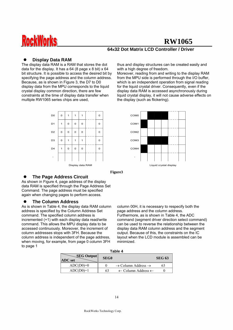
RW1065 64x32 Dot Matrix LCD Controller Driver
RockWorks Technology Corp
14
Display Data RAM The display data RAM is a RAM that stores the dot data for the display It has a 64 (8 page x 8 bit) x 64 bit structure It is possible to access the desired bit by specifying the page address and the column addressBecause as is shown in Figure 3 the D7 to D0 display data from the MPU corresponds to the liquid crystal display common direction there are few constraints at the time of display data transfer when multiple RW1065 series chips are used
thus and display structures can be created easily and with a high degree of freedom Moreover reading from and writing to the display RAM from the MPU side is performed through the IO buffer which is an independent operation from signal reading for the liquid crystal driver Consequently even if the display data RAM is accessed asynchronously during liquid crystal display it will not cause adverse effects on the display (such as flickering)
0
1
0
0
1
1
0
0
1
0
1
0
0
1
0
1
0
0
1
0
0
0
0
0
0
D0
D1
D2
D3
D4
-
Display data RAM Liquid crystal display
COM0
COM1
COM2
COM3
COM4
-
Figure3
The Page Address Circuit As shown in Figure 4 page address of the display data RAM is specified through the Page Address Set Command The page address must be specified again when changing pages to perform access
The Column Address As is shown in Table 4 the display data RAM column address is specified by the Column Address Set command The specified column address is incremented (+1) with each display data readwrite command This allows the MPU display data to be accessed continuously Moreover the increment of column addresses stops with 3FH Because the column address is independent of the page address when moving for example from page 0 column 3FH to page 1
column 00H it is necessary to respecify both the page address and the column address Furthermore as is shown in Table 4 the ADC command (segment driver direction select command) can be used to reverse the relationship between the display data RAM column address and the segment output Because of this the constraints on the IC layout when the LCD module is assembled can be minimized
Table 4 SEG Output
ADC set SEG0 SEG 63
ADC(D0)=0 0 rarr Column Address rarr 63 ADC(D0)=1 63 larr Column Address larr 0
RW1065 64x32 Dot Matrix LCD Controller Driver
RockWorks Technology Corp
15
Figure 4
Page Address D3 D2 D1 D0
DataSE
G0
SEG
1
SEG
2
SEG
3
SEG
4
SEG
5
SEG
6
SEG
7
SEG
8
helliphelliphelliphellip
SEG
55
SEG
56
SEG
57
SEG
58
SEG
59
SEG
60
SEG
61
SEG
62
SEG
63 SEG
COM
D0 COM0
D1 COM1
D2 COM2
D3 COM3
D4 COM4
D5 COM5
D6 COM6
0 0 0 0
D7
Page 0
COM7
D0 COM8
D1 COM9
D2 COM10
D3 COM11
D4 COM12
D5 COM13
D6 COM14
0 0 0 1
D7
Page 1
COM15
D0 COM16
D1 COM17
D2 COM18
D3 COM19
D4 COM20
D5 COM21
D6 COM22
0 0 1 0
D7
Page 2
COM23
D0 COM24
D1 COM25
D2 COM26
D3 COM27
D4 COM28
D5 COM29
D6 COM30
0 0 1 1
D7
Page 3
COM31
ADC=0 00
01
02
03
04
05
06
07
08
helliphelliphelliphellip 55
56
57
58
59
60
61
62
63
COLUMN ADC=1 63
62
61
60
59
58
57
56
55
helliphelliphelliphellip 08
07
06
05
04
03
02
01
00
RW1065 64x32 Dot Matrix LCD Controller Driver
RockWorks Technology Corp
16
Common Timing Generator Circuit Display Data Latch Circuit Generates common timing signals and FR frame signals from the CL basic clock The 132 or 164 duty (for RW1065) can be selected by the Duty Select command The 132 and 164 duties are provided by two chips consisting of the master and slave chips in the common multi-chip mode
This latch stores one line of display data for use by the LCD driver interface circuitry The output of this latch is controlled by the Display ONOFF
132 duty
164 duty
SHL=0
SHL=1
SHL=0
SHL=1
RW1065 64x32 Dot Matrix LCD Controller Driver
RockWorks Technology Corp
17
Display Timing Generator Circuit
The display timing generator circuit generates the timing signal to the line address circuit and the display data latch circuit using the display clock The display data is latched into the display data latch circuit synchronized with the display clock and is output to the data driver output terminal Reading to the display data liquid crystal driver circuits is completely independent of accesses to the display data RAM by the MPU Consequently even if the display data
RAM is accessed asynchronously during liquid crystal display there is absolutely no adverse effect (such asflickering) on the display Moreover the display timing generator circuit generates the common timing and the liquid crystal alternating current signal (FR) from the display clock It generates a drive wave form using a 2 frame alternating current drive method as is shown in Figure 5 for the liquid crystal drive circuit
Two-frame alternating current drive waveform
Figure 5
When multiple RW1065 Series chips are used the slave chip must be supplied the display timing signals(FR CL) from the master chip
Table 5 shows the status of the FR and CL signals
Table 5 Operating Mode FR CL
Master (MS = ldquoHrdquo) The internal oscillator circuit is enabled (CLS = ldquoHrdquo) The internal oscillator circuit is disabled (CLS = ldquoLrdquo)
Output Output
Output Input
Slave (MS = ldquoLrdquo) The internal oscillator circuit is enabled (CLS = ldquoHrdquo) The internal oscillator circuit is disabled (CLS = ldquoLrdquo)
Input Input
Input Input
RW1065 64x32 Dot Matrix LCD Controller Driver
RockWorks Technology Corp
18
The Liquid Crystal Driver Circuits
These are a 64-channel (RW1065) that generate four voltage levels for driving the liquid crystal The combination of the display data the COM scan signal and the FR signal
produces the liquid crystal drive voltage output Figure 6 shows examples of the SEG and COM output waveform
Figure 6
RW1065 64x32 Dot Matrix LCD Controller Driver
RockWorks Technology Corp
19
The Power Supply Circuit
The power supply circuits are low-power consumption power supply circuits that generate the voltage levels required for the liquid crystal drivers They comprise Booster circuits and voltage follower circuits They are only enabled in master operation The power supply circuits can turn on automatically after power on
Consequently it is possible to make an external power supply and the internal power supply function somewhat in parallel
The Liquid Crystal Voltage Generator Circuit The V0 voltage is produced by a resistive voltage divider outside the IC through VRAB pin and can be produced at the V1 V2 V3 and V4 voltage levels required for liquid crystal driving Moreover when the voltage follower changes the impedance it provides V1 V2 V3 and V4 to the liquid crystal drive circuit 15 bias or 16 bias or 18 bias or 19 bias for RW1065 can be selected by BS0 and BS1 pins V0-Vss maximum voltage is 15V Vout-Vss maximum voltage is 17V If VDD lt 35V it can use the Booster circuit 2x3x4xThe booster voltage can follow the spec condition (Vout-Vss ≦ 17V max voltage) if VDD gt35V only use the 2X3X booster circuit that can ensure the V0-Vss voltage ≦ 15V If use the VDD voltage 5V and 4X booster itrsquos over the spec operation condition To turn on built-in power (boosterfollower) must waiting 200mS to display on for boosterfollower stable Therefore power off must follower ldquopower off sequencerdquo too
Power on Display off
Power off
Power off sequence
Wait time gt200mS
Display on
Power on sequence
RW1065 64x32 Dot Matrix LCD Controller Driver
RockWorks Technology Corp
20
The Reset Circuit
When the RTP input comes to the ldquoLrdquo level these LSIs return to the default state Their default states are as follows 1 Display OFF 2 Display all point on is select to normal 3 Display normalreverse is select to normal 4 164 duty is selected 5 Read modify write OFF 6 Column address set to Address 0 7 Page address set to Page 0 8 Start line set to first line 9 Frame frequency set to default 10 Power save mode released 11 Ext set to ldquo0rdquo When the power is turned on the IC internal state becomes unstable and it is necessary to initialize it using the RSTP terminal After the initialization each input terminal should be controlled normally While RSTP is ldquoLrdquo the oscillator works but the display timing generator stops and the CL FR terminals are fixed to ldquoHrdquo The terminals D0 to D7 are not affected
RW1065 64x32 Dot Matrix LCD Controller Driver
RockWorks Technology Corp
21
TABLE OF RW1065 INSTRUCTIONS
Instruction code Instruction RS RW DB7 DB6 DB5 DB4 DB3 DB2 DB1 DB0 Description
EXT=0 or 1
MODE SET 0 0 0 0 0 0 1 1 0 EXT Set EXT mode
Instruction code Instruction RS RW DB7 DB6 DB5 DB4 DB3 DB2 DB1 DB0 Description
EXT=0 Display ONOFF 0 0 0 0 1 1 1 1 1 D D=0Display OFF
D=1Display ONSet page address 0 0 1 0 1 1 1 P2 P1 P0 Set page address
Set column address 0 0 0 1 Y5 Y4 Y3 Y2 Y1 Y0 Set column
address MSB
Read Status 0 1 BUSY 0 ON OFF RESET 0 0 0 0 Read register
status Write display
data 1 0 Write data Write data into DDRAM
Read display data 1 1 Read data Read data from
DDRAM Set initial
display line register
0 0 1 1 S5 S4 S3 S2 S1 S0 Specify the initial
display line to realize vertical scrolling
Instruction code Instruction RS RW DB7 DB6 DB5 DB4 DB3 DB2 DB1 DB0 Description
EXT=1
NOP 0 0 0 0 0 0 0 0 0 0 no operation
Set modiy-read 0 0 0 0 0 0 1 0 0 0 Set modiy-read
mode
END 0 0 0 0 0 0 1 1 1 0 release modiy-read mode
Set power save mode 0 0 0 0 0 0 0 0 1 PSAVE P=0 normal mode
P=1 sleep mode
0 0 0 0 0 1 0 1 Display
COMMAND (double
command)
0 0 FRSEL
0 0 0 0 REV ALLON DUTY
DUTY=1 64 duty DUTY=0 32 duty ALLON=1display all on ALLON=0display
normal REV=1display reverse REV=0display normal FRSEL=1FR frequency double default FRSEL=0FR frequency default
RW1065 64x32 Dot Matrix LCD Controller Driver
RockWorks Technology Corp
22
Command Description
See the Table of RW1065 instructions The RW1065 series identifies a data bus using a combination of RS E and RW signals As the MPU translates a command in the internal timing only (independent from the external clock) its speed is very high The busy check is usually not required
Display ONOFF
EXT RS RW D7 D6 D5 D4 D3 D2 D1 D0
0 0 0 0 0 1 1 1 1 1 D
This command turns the display on and off D=1 Display ON D=0 Display OFF(default)
Set page Address This command specifies the page address that corresponds to the low address of the display data RAM when it is accessed by the MPU Any bit of the display data RAM can be accessed when its page address and column address are specified The display status is not changed even when the page address is changed
EXT RS RW D7 D6 D5 D4 D3 D2 D1 D0
0 0 0 1 0 1 1 1 A2 A1 A0
This command loads the page address register
A2 A1 A0 Page
0 0 0 0 (default)
0 0 1 1 0 1 0 2 0 1 1 3 1 0 0 4 1 0 1 5 1 1 0 6 1 1 1 7
Page mapping see Figure 4
RW1065 64x32 Dot Matrix LCD Controller Driver
RockWorks Technology Corp
23
Set Column Address This command specifies a column address of the display data RAM When the display data RAM is accessed by the MPU continuously the column address is incremented by I each time it is accessed from the set address Therefore the MPU can access to data continuously The column address stops to be incremented at address 63 and the page address is not changed continuously
EXT RS RW D7 D6 D5 D4 D3 D2 D1 D0
0 0 0 0 1 A5 A4 A3 A2 A1 A0
A5 A4 A3 A2 A1 A0 Column Address0 0 0 0 0 0 0(default) 0 0 0 0 0 1 1
1 1 1 1 1 1 63
Read Status
EXT RS RW D7 D6 D5 D4 D3 D2 D1 D0
0 0 1 BUSY 0 ON OFF RESET 0 0 0 0
The BUSY Flag bit indicates that RW 1065 is operating or no operating
BUSY=1 Operation BUSY=0 Ready
The ONOFF bit indicates the current status of the display It is the inverse of the polarity of the display ONOFF command ONOFF=1 Display OFF ONOFF=0 Display ON The RESET bit indicates whether the driver is executing a hardware or software reset or if it is in normal operating mode RESET=1 Currently executing reset command RESET=0 Normal operation
RW1065 64x32 Dot Matrix LCD Controller Driver
RockWorks Technology Corp
24
Write Display Data
EXT RS RW D7 D6 D5 D4 D3 D2 D1 D0
0 1 0 Write data
Writes 8-bits of data into the display data RAM at a location specified by the contents of the column address and page address registers and then increments the column address register by one
Read Display Data
EXT RS RW D7 D6 D5 D4 D3 D2 D1 D0
0 1 1 Read data
Reads 8-bits of data from the data IO latch updates the contents of the IO latch with display data from the display data RAM location specified by the contents of the column address and page address registers and then increments the column address register After loading a new address into the column address register one dummy read is required before valid data is obtained
Set initial display line register
EXT RS RW D7 D6 D5 D4 D3 D2 D1 D0
0 0 0 1 1 S5 S4 S3 S2 S1 S0
Loads the RAM line address of the initial display line COM 0 into the initial display line register The RAM display data becomes the top line of the LCD screen It is followed by the higher number lines in ascending order corresponding to the duty cycle The screen can be scrolled using this command by incrementing the line address(default value=rdquo00Hrdquo)
RW1065 64x32 Dot Matrix LCD Controller Driver
RockWorks Technology Corp
25
Read-Modify-Write
EXT RS RW D7 D6 D5 D4 D3 D2 D1 D0
1 0 0 0 0 0 0 1 0 0 0
This command defeats column address register auto-increment after data reads The current contents of the column Address register are saved The mode remains active until an End command is received When the End command is entered the column address is returned to the one used during input of Read-Modify-Write Command This function can reduce the load of MPU when data change is repeated as a specific display area Any command other than Data Read or Write can be used in the Read-Modify-Write mode However the Column Address Set command cannot be used
End
EXT RS RW D7 D6 D5 D4 D3 D2 D1 D0
1 0 0 0 0 0 0 1 1 1 0
This command cancels read-modify-write mode and restores the contents of the column address register to their value prior to the receipt of the Read-Modify-Write command
N N+1 N+2 N+3 N+m N
Read -modify-write mode set End
Returm
Column address
Set page address
Set column address
Read-modify-write
Dummy read
Read data
Write data
End
CompletedNo
Yes
RW1065 64x32 Dot Matrix LCD Controller Driver
RockWorks Technology Corp
26
Set power save mode
EXT RS RW D7 D6 D5 D4 D3 D2 D1 D0
1 0 0 0 0 0 0 0 0 1 PSAVE
When power save mode is entered thus greatly reducing power consumption In the power save mode the display data is saved as is the operating mode that was in effect before the power saver mode was initiated and the MPU is still able to access the display data RAM PSAVE=1 Sleep mode PSAVE=0 Normal mode Sleep mode This stops all operations in the LCD display system and as long as there are no accesses from the MPU the consumption current is reduced to a value near the static current The internal modes during sleep mode are as follows 1 The oscillator circuit and the LCD power supply circuit are halted 2 All liquid crystal drive circuits are halted and the segment and common drive outputs output a Vss level
Display command double command
EXT RS RW D7 D6 D5 D4 D3 D2 D1 D0
1 0 0 0 0 0 0 0 1 0 1
1 0 0 FRSEL 0 0 0 0 REV ALLON DUTY
Display NormalReverse set REV=1 Reverse REV=0 Normal(default) Display All Point ONOFF ALLON=1 All display points ON ALLON=0 Normal(default) Select Duty Duty=1 164 duty cycle(default) Duty=0 132 duty cycle FRAME FREQUENCY Select FRSEL=1 Double FRSEL=0 (default)
RW1065 64x32 Dot Matrix LCD Controller Driver
RockWorks Technology Corp
27
Hardware Pin Set
Select ADC by ADC Pin The pin selects the relationship between display data RAM column addresses and segment drivers ADC=1 SEG0larrcolumn address 3FHhellipinverted ADC=0 SEG0larrcolumn address 00Hhellipnormal(default) This command is provided to reduce restrictions on the placement of driver ICs and routing of traces during printed circuit Board design See Figure 4 for a table of segments and column addresses for the two values of D
Select SHL by SHL Pin The pin selects the com output scan direction SHL=1 Reverse directioncom63rarrcom0 SHL=0 Normal com0rarrcom63 Both master and slave should set identical SHL value
Select LCD Bias by BS0 BS1 Pin
BS1 BS0 Bias 0 0 15 bias 0 1 16 bias 1 0 18 bias 1 1 19 bias
RW1065 64x32 Dot Matrix LCD Controller Driver
RockWorks Technology Corp
28
When an External Resistance is Used The liquid crystal power supply voltage V0 is set by adding resistors Rarsquo and Rbrsquo between VDD and VR and between VR and V0 respectively
RW1065
RW1065 64x32 Dot Matrix LCD Controller Driver
RockWorks Technology Corp
29
The set voltage circuits
Using the step-up voltage circuits equipped within the RW1065 chips it is possible to produce a 2X 3X 4X step-up voltage levels 2X step-up
To produce voltage level in the positive direction at the Vout terminal that is 2 times the voltage difference between VSS and VDD2 Please configure set voltage circuits like this Place a 1uF~22uF capacitor between CAP1N and CAP1P Place a 1uF~22uF capacitor between VSS and VOUT Short CAP2P CAP3P and VOUT Leave CAP2N open 3X step-up
To produce voltage level in the positive direction at the Vout terminal that is 3 times the voltage difference between VSS and VDD2 Please configure set voltage circuits like this Place a 1uF~22uF capacitor between CAP1N and CAP1P Place a 1uF~22uF capacitor between VSS and VOUT Place a 1uF~22uF capacitor and 100 ohms resistor between CAP2N and CAP2P Short CAP3P and Vout 4X step-up
To produce voltage level in the positive direction at the Vout terminal that is 4 times the voltage difference between VSS and VDD2 Please configure set voltage circuits like this Place a 1uF~22uF capacitor between CAP1N and CAP1P Place a 1uF~22uF capacitor between VSS and VOUT Place a 1uF~22uF capacitor and 100 ohms resistor between CAP2N and CAP2P Place a 1uF~22uF capacitor and 100 ohms resistor between CAP1N and CAP3P
RW1065 64x32 Dot Matrix LCD Controller Driver
RockWorks Technology Corp
30
ABSOLUTE MAXIMUM RATINGS Characteristics Symbol Value Unit
Power supply voltage VDD -03 to +70 V
LCD driver voltage Vout 0 to +17 V
Input voltage VIN -03 to VDD+03 V
Operating temperature TA -40 to +85
Storage temperature TSTO -55 to +125
DC CHARACTERISTICS
Rating Item Symbol Condition Min Typ Max Unit ApplicablePin
Operating Voltage VDD - 27 30 55 V VDD1
Step up output voltage Vout (Relative to VDD) 0 - 17 V Vout
Voltage follower circuit operating Voltage V0 (Relative to VDD) 0 - 15 V V0
V0 accuracy V0 - 0 - 15 V0
High-level Input Voltage Low-level Input Voltage
VIHC VILC - 07 VDD
Vss - VDD 09 V 2
High-level Output Voltage Low-level Output Voltage
VOHC VOLC
IOH = ndash05 mA IOL = 05 mA
08VDD Vss - VDD
02 VDD V 3
Input leakage current ILI VIN = VDD or VSS -1 - 2 uA 4
Output leakage current ILO - -1 1 uA 5
Liquid Crystal Driver ON Resistance RON
Ta= 25degC(Relative To VDD)
V0 =15 V - 16 20 KΩ SEGn COMn 6
Internal Oscillator fOSC 2286 254 2794 Oscillator
Frequency External Input RECOMMAND fCL
Ta = 25degC 132Duty 2286 254 2794
kHz CL
Internal Oscillator fOSC 45 5 55 Oscillator
Frequency External Input RECOMMAND fCL
Ta = 25degC 164Duty 45 5 55
kHz CL
bullDynamic Consumption Current During Display with the Internal Power Supply OFF Current consumed by total ICs when an external power supply is used
Unless otherwise specified Vss=0V VDD=30V
RW1065 64x32 Dot Matrix LCD Controller Driver
RockWorks Technology Corp
31
Display Pattern OFF
Ta = 25degC Vout=17V Rating Item Symbol Condition Min Typ Max Unit Notes
VDD=30 V V0-Vss=8V - 10 15 RW1065 IDD VDD=50 V V0-Vss=8V - 35 45
microA 7
Display Pattern Checker
Ta = 25degC Vout=17V Rating Item Symbol Condition Min Typ Max Unit Notes
VDD=30 V V0-Vss=8V - 15 20 RW1065 IDD VDD=50 V V0-Vss=8V - 40 50
microA 7
Display Pattern OFF
Ta = 25degC Vout=17V Rating Item Symbol Condition Min Typ Max Unit Notes
VDD=30 V V0-Vss=8V - 15 20 RW1065 IDD VDD=50 V V0-Vss=8V - 40 50
microA 7
Display pattern Checker
Ta = 25degC Vout=17V Rating Item Symbol Condition Min Typ Max Unit Notes
VDD=30 V V0-Vss=8V - 65 80 RW1065 IDD VDD=50 V V0-Vss=8V - 130 150
microA 7
bull Consumption Current at Time of Power Saver Mode VSS = 0 V VDD = 30 V plusmn 10
Rating Item Symbol Condition Min Typ Max Unit Notes
Sleep mode IDD - - 5 10 microA -
References for items market with 1 While a broad range of operating voltages is guaranteed performance cannot be guaranteed if there are sudden fluctuations to the
voltage while the MPU is being accessed 2 The RS D0 to D5 D6 D7 E RW CS1BP CS2P CLS CL FR MS and RST
― terminals
3 The D0 to D7 FR and CL terminals 4 The RS E RW CS1BP CS2P CLS MS and RST
― terminals
5 Applies when the D0 to D5 D6 D7 CL and FR terminals are in a high impedance state 6 These are the resistance values for when a 01 V voltage is applied between the output terminals SEGn or COMn and
the various power supply terminals (V1 V2 V3 and V4) These are specified for the operating voltage (3) range RON = 01 V ∆I (Where ∆I is the current that flows when 01 V is applied while the power supply is ON)
7 It indicates the current consumed on ICs alone when the internal oscillator circuit and display are turned on Does not include the current due to the LCD panel capacity and wiring capacity Applicable only when there is no access from the MPU
RW1065 64x32 Dot Matrix LCD Controller Driver
RockWorks Technology Corp
32
TIMING CHARACTERISTICS
68 Interface
(Ta=-40 to 85 degC) VDD=27 to 45V
Rating VDD=45 to 55V
Rating Item Signal Symbol ConditionMin Max Min Max
Units
Address hold time RS tAH6 0 mdash 0 mdash Address setup time RS tAW6
mdash 0 mdash 0 mdash
ns
System cycle time RS tCYC6 mdash 900 mdash 800 mdash ns Data setup time D0 to D7 tDS6 100 mdash 100 mdash Data hold time D0 to D7 tDH6
mdash 0 mdash 0 mdash
ns
Access time D0 to D7 tACC6 mdash 350 mdash 250
Output disable time D0 to D7 tOH6 CL = 100 pF
mdash 300 mdash 200 ns
Read tEWHR 360 mdash 300 mdash Enable H pulse time
WriteE
tEWHW mdash
360 mdash 300 mdash ns
Read tEWLR 450 mdash 400 mdash Enable L pulse time
WriteE
tEWLW mdash
450 mdash 400 mdash ns
1 All timing is specified using 20 and 80 of VDD as the reference 2 tEWLW and tEWLR are specified as the overlap between CS1BP being ldquoLrdquo (CS2P = ldquoHrdquo) and E
RW1065 64x32 Dot Matrix LCD Controller Driver
RockWorks Technology Corp
33
Reset Timing
Rating Item Signal Symbol Condition
Min Typ Max Units
Reset time mdash tR mdash mdash - 2 micros
Reset ldquoLrdquo pulse width RST tRW mdash 2 - mdash micros
1 When double chip was be used then the duty set command must be set between the tR
RW1065 64x32 Dot Matrix LCD Controller Driver
RockWorks Technology Corp
34
IO PAD CONFIGURATION
RW1065 64x32 Dot Matrix LCD Controller Driver
RockWorks Technology Corp
35
THE MPU INTERFACE (REFERENCE EXAMPLES) The RW1065 Series can be connected to 6800 Series MPUs The display area can be enlarged by using multiple RW1065 Series chips When this is done the chip select signal can be used to select the individual ICs to access
6800 Series MPUs
RW
106
5
RW1065 64x32 Dot Matrix LCD Controller Driver
RockWorks Technology Corp
36
When using external multi-level power supply for LCD driving (REFERENCE EXAMPLE)
Using a resistor divider can provide RW1065 external multi-level power supply for LCD driving
The circuit below shows a resistor divider network which can bias V0 V1 V2 V3 and V4 externally
RW1065 64x32 Dot Matrix LCD Controller Driver
RockWorks Technology Corp
37
bullWhen V0 V1 V2 V3 and V4 are biased by external power supply analog section of RW1065 should be turn off by software during LCD initialization The example in below shows the sequence to turn off analog section when external bias is used Begin of LCD initialization 1 Reset RW1065 2 SET EXT=1 (mode instruction)
RS RW DB7 DB6 DB5 DB4 DB3 DB2 DB1 DB00 0 0 0 0 0 1 1 0 1
3 SET Display Command (double command)
RS RW DB7 DB6 DB5 DB4 DB3 DB2 DB1 DB00 0 0 0 0 0 0 1 0 1 0 0 0 0 1 1 0 0 0 1
4 SET EXT=1 (mode instruction)
RS RW DB7 DB6 DB5 DB4 DB3 DB2 DB1 DB00 0 0 0 0 0 1 1 0 0
End of LCD initialization
bullBecause pins can not set LCD bias when external power supplies are used for LCD driving the bias can be set by an appropriate configuration for a resistor voltage divider networks The example is shown below
VSS
R
R
NR
R
R
RV1
RV2
RV3
RV4
V0
Bias Network Circuit Concept 15 Bias N=1 total = 5R 16 Bias N=2 total =6R 18 Bias N=4 total =8R 19 Bias N=5 total = 9R
RW1065 64x32 Dot Matrix LCD Controller Driver
RockWorks Technology Corp
38
Single chip solution for RW1065 application (REFERENCE EXAMPLE)
For a 64x32 application the duty cycle of LCD panel is 164 and the display duty of RW1065 should be set to 164 The display duty cycle can be selected by the DUTY bit in display command The diagram for 64x32 application is shown below
64 SEGx32COM LCD Panel
164 duty cycle
RW1065 DUTY=1
COM1~33
SEG1~65
RW1065 64x32 Dot Matrix LCD Controller Driver
RockWorks Technology Corp
39
Using an adjustable resistor on the main board to adjust the contrast of liquid crystal display (REFERENCE EXAMPLE)
The schematic shows an adjustable resistor on main board that can adjust voltage level of V0
RW1065 64x32 Dot Matrix LCD Controller Driver
RockWorks Technology Corp
40
Package information (Please pay close attention to the information in this section Do not hesitate to consult with our sale representative if you have any question or concern)
In order to make better bonding yield for RW1065 please follow the tips and recommendations in this section In this section few tips about COB footprint style PCB layout and wire bonding will be discussed
The drawing in below shows the PCB footprint style which we recommend for RW1065 Pads array in
curve shape is easier for Al wire bonding Besides that a real size COB footprint for RW1065 is also shown in below RW1065 COB footprint is also available in powerpcb or protel format for design reference purpose
The ratio is 11
RW1065 64x32 Dot Matrix LCD Controller Driver
RockWorks Technology Corp
41
During COB footprint design there have some tips about footprint that the PCB designer should know The angle between bonding wire and vertical line should less than 45 Otherwise the wire shorts would become very easy to happen at fours corners of the chip
The angle between bonding wire and vertical line could be reduced by expanding the distance between pads array and the chip In addition reducing length in horizon direction of pads array could minimize the angle between bonding wire and vertical line The picture in below will help to illustrate this concept From the experiences COB footprint style affects the bonding yield
Bad Wires are too close to each other
The angle between bonding wire and vertical line is greater than 45
The angle between bonding wire and vertical line is less than 45
Wires are not too close to each other
Reducing length in horizon direction of pads array could minimize the angle between bonding wire and vertical line
The angle between bonding wire and vertical line could be reduced by expanding the distance between pads array and the chip
RW1065 64x32 Dot Matrix LCD Controller Driver
RockWorks Technology Corp
42
If the gap between pads of COB footprint is filled with solder mask coating it is difficult to bond Al wire to
the pads The top solder masks layer that overlap COB footprint area should be removed
Please use 1 mils diameter Al wire for RW1065 wire bonding
1 2 3 4 5 6
A
B
C
D
654321
D
C
B
A
Title
Number RevisionSize
C
Date 29-Aug-2007 Sheet of File D公司資料99seMyDesignddb Drawn By
RW1065
COM131
COM142
COM153
COM164
COM175
COM186
COM197
COM208
COM219
COM2210
COM2311
COM2412
COM2513
COM2614
COM2715
COM2816
COM2917
COM3018
COM3119
SEG
6320
SEG
6221
SEG
6122
SEG
6023
SEG
5924
SEG
5825
SEG
5726
SEG
5627
SEG
5528
SEG
5429
SEG
5330
SEG
5231
SEG
5132
SEG
5033
SEG
4934
SEG
4835
SEG
4736
SEG
4637
SEG
4538
SEG
4439
SEG
4340
SEG
4241
SEG
4142
SEG
4043
SEG
3944
SEG
3845
SEG
3746
SEG
3647
SEG
3548
SEG
3449
SEG
3350
SEG
3251
SEG
3152
SEG
3053
SEG
2954
SEG
2855
SEG
2756
SEG
2657
SEG
2558
SEG
2459
SEG
2360
SEG
2261
SEG
2162
SEG
2063
SEG
1964
SEG
1865
SEG
1766
SEG
1667
SEG
1568
SEG
1469
SEG13 70SEG12 71SEG11 72SEG10 73SEG9 74SEG8 75SEG7 76SEG6 77SEG5 78SEG4 79SEG3 80SEG2 81SEG1 82SEG0 83ADCP 84CLL 85
VSS
86D
087
D1
88D
289
D3
90D
491
D5
92D
693
D7
94C
S1B
P95
CS2
P96
ERD
P97
AO
P(R
S)98
RW
RP
99V
DD
100
RST
P10
1C
LSP
102
FRR
103
MSP
104
BS1
P10
5B
S0P
106
SHLP
107
VD
D2
108
CA
P2N
109
CA
P2P
110
CA
P1P
111
CA
P1N
112
CA
P3P
113
VO
UT
114
V0
115
VR
AB
116
V3
117
V2
118
V4
119
V1
120
CO
M0
121
CO
M1
122
CO
M2
123
CO
M3
124
CO
M4
125
CO
M5
126
CO
M6
127
CO
M7
128
CO
M8
129
CO
M9
130
CO
M10
131
CO
M11
132
CO
M12
133
4897x1902 um
IC1
RW1065
C9CAPR4
100R0603
R30R0603
C8
CAP
C7
CAP
R2
100R0603
R1
0R0603C6 22uf
R50R
R6300R
R7RES1
R8NC R9
100R0603
VDD
R10
NC
R11
100R0603
R12
100R0603
R13
NC
R14
100R0603
R15
NC
VDD
D0
D1
D2
D3
D4
D5
D6
D7
DB[07]
VDDC5
01uf0603
VD
D
CS2
P
123456789
1011121314151617181920
J1
CON20
C1201uf0603
R3951K0603
VDD
CAP Value1UF~22UF
2XPut C6C8 Short R1R3Open R2R4C7C93XPut C6C8C9 R4Short R1Open R2R3C74XOpen R1R3
BS0 BS1 Bias0 0
0 1
1 0
11
15 bias
16 bias
18 bias
19 bias
ADC=0 SEG0lt~column address 00Hnormal(default) ADC=1 SEG0lt~column address 3FHinverted
SHL=0 Normal COM0~gtCOM63(default)SHL=1 Reverse direction COM63~gtCOM0
R16100R0603
LCD PANEL 64X32RockWorks
RW1065 64X32
COM0-31 SEG0-63SHL=0 ADC=0
SHL=1COM31-0
ADC=1SEG63-0
if use single chip for 32 command displaythe display command must select 164 dutyDisplay panel must select 164 duty type
VO
UT
C3P
C1N
C1P
C2P
C2N
VDD2
ADC
SHL
BS0
BS1
CLLADC
V1
V2
V3
V4
VR
AB
V0
VO
UT
C3P
C1N
C1P
C2P
C2N
VD
D2
SHL
BS0
BS1
FRR
RST
P
RW
RS
E CS1
B
CS1
V0RSRWED0D1D2D3D4D5D6D7
RSTPAK
C4
22uf
RBRES1
RA1RES1
C2
22uf
C1
22uf
C3
22uf
C0
22uf
R20
100k0603
R21
100k0603
R17
200K0603
V1
V2
V3
V4 VRAB
V0
V0
OPTION
B
R18
300R0603
RA2RES1
VADJ
R19100R
R23 RES1R22 0R
R24
RES1
R25
0R
VDD
CS1BP
CS2P
CS1
CS1
R26
22R0603
R27
22R0603
C1047uf
C11
01uf
VSS_INVDD_IN
D1DIODE
FGND
鐵框地
VSS
VDD
R28 10RR29 10RR30 10RR31 10RR32 10RR33 10RR34 10RR35 10RR36 10RR37 10RR38 10R
VADJ
1 2 3 4 5 6
A
B
C
D
654321
D
C
B
A
Title
Number RevisionSize
C
Date 29-Aug-2007 Sheet of File D公司資料99seMyDesignddb Drawn By
RW1065
COM131
COM142
COM153
COM164
COM175
COM186
COM197
COM208
COM219
COM2210
COM2311
COM2412
COM2513
COM2614
COM2715
COM2816
COM2917
COM3018
COM3119
SEG
6320
SEG
6221
SEG
6122
SEG
6023
SEG
5924
SEG
5825
SEG
5726
SEG
5627
SEG
5528
SEG
5429
SEG
5330
SEG
5231
SEG
5132
SEG
5033
SEG
4934
SEG
4835
SEG
4736
SEG
4637
SEG
4538
SEG
4439
SEG
4340
SEG
4241
SEG
4142
SEG
4043
SEG
3944
SEG
3845
SEG
3746
SEG
3647
SEG
3548
SEG
3449
SEG
3350
SEG
3251
SEG
3152
SEG
3053
SEG
2954
SEG
2855
SEG
2756
SEG
2657
SEG
2558
SEG
2459
SEG
2360
SEG
2261
SEG
2162
SEG
2063
SEG
1964
SEG
1865
SEG
1766
SEG
1667
SEG
1568
SEG
1469
SEG13 70SEG12 71SEG11 72SEG10 73SEG9 74SEG8 75SEG7 76SEG6 77SEG5 78SEG4 79SEG3 80SEG2 81SEG1 82SEG0 83ADCP 84CLL 85
VSS
86D
087
D1
88D
289
D3
90D
491
D5
92D
693
D7
94C
S1B
P95
CS2
P96
ERD
P97
AO
P(R
S)98
RW
RP
99V
DD
100
RST
P10
1C
LSP
102
FRR
103
MSP
104
BS1
P10
5B
S0P
106
SHLP
107
VD
D2
108
CA
P2N
109
CA
P2P
110
CA
P1P
111
CA
P1N
112
CA
P3P
113
VO
UT
114
V0
115
VR
AB
116
V3
117
V2
118
V4
119
V1
120
CO
M0
121
CO
M1
122
CO
M2
123
CO
M3
124
CO
M4
125
CO
M5
126
CO
M6
127
CO
M7
128
CO
M8
129
CO
M9
130
CO
M10
131
CO
M11
132
CO
M12
133
4897x1902 um
IC1
RW1065 Master
RW1065
COM131
COM142
COM153
COM164
COM175
COM186
COM197
COM208
COM219
COM2210
COM2311
COM2412
COM2513
COM2614
COM2715
COM2816
COM2917
COM3018
COM3119
SEG
6320
SEG
6221
SEG
6122
SEG
6023
SEG
5924
SEG
5825
SEG
5726
SEG
5627
SEG
5528
SEG
5429
SEG
5330
SEG
5231
SEG
5132
SEG
5033
SEG
4934
SEG
4835
SEG
4736
SEG
4637
SEG
4538
SEG
4439
SEG
4340
SEG
4241
SEG
4142
SEG
4043
SEG
3944
SEG
3845
SEG
3746
SEG
3647
SEG
3548
SEG
3449
SEG
3350
SEG
3251
SEG
3152
SEG
3053
SEG
2954
SEG
2855
SEG
2756
SEG
2657
SEG
2558
SEG
2459
SEG
2360
SEG
2261
SEG
2162
SEG
2063
SEG
1964
SEG
1865
SEG
1766
SEG
1667
SEG
1568
SEG
1469
SEG13 70SEG12 71SEG11 72SEG10 73SEG9 74SEG8 75SEG7 76SEG6 77SEG5 78SEG4 79SEG3 80SEG2 81SEG1 82SEG0 83ADCP 84CLL 85
VSS
86D
087
D1
88D
289
D3
90D
491
D5
92D
693
D7
94C
S1B
P95
CS2
P96
ERD
P97
AO
P(R
S)98
RW
RP
99V
DD
100
RST
P10
1C
LSP
102
FRR
103
MSP
104
BS1
P10
5B
S0P
106
SHLP
107
VD
D2
108
CA
P2N
109
CA
P2P
110
CA
P1P
111
CA
P1N
112
CA
P3P
113
VO
UT
114
V0
115
VR
AB
116
V3
117
V2
118
V4
119
V1
120
CO
M0
121
CO
M1
122
CO
M2
123
CO
M3
124
CO
M4
125
CO
M5
126
CO
M6
127
CO
M7
128
CO
M8
129
CO
M9
130
CO
M10
131
CO
M11
132
CO
M12
133
4897x1902 um
IC2
RW1065 Slave
C4
22uf
RBRES1
RA1RES1
C2
22uf
C1
22uf
C3
22uf
C0
22ufC9CAPR4
100R0603
R30R0603
C8
CAP
C7
CAP
R2
100R0603
R1
0R0603C6 22uf
R50R0603
R6300R0603
R7RES1
R8NC R9
100R0603
VDD
R10
NC
R11
100R0603
R12
NC
R13
100R0603
R14
100R0603
R15
NC
R16
100R0603
R17
NC
VDD
D0
D1
D2
D3
D4
D5
D6
D7
D0
D1
D2
D3
D4
D5
D6
D7
DB[07] DB[07]
VDDC10
01uf0603
VD
D
IC1_
CS2
P
VDD
IC2_
CS2
P
VD
D
C11
01uf0603
VSS
VSS
LCD PANEL 128X64
Master COM0-31 Slave COM32-63
Master SEG0-63 Slave SEG64-127
123456789
1011121314151617181920
J1
CON20
Master Slave
CAP Value1UF~22UF
2XPut C6C8 Short R1R3Open R2R4C7C93XPut C6C8C9 R4Short R1Open R2R3C74XOpen R1R3
RockWorksRW1065 128x64
BS0 BS1 Bias0 0
0 1
1 0
11
15 bias
16 bias
18 bias
19 bias
ADC=0 SEG0lt~column address 00Hnormal(default) ADC=1 SEG0lt~column address 3FHinverted
SHL=0 Normal COM0~gtCOM63(default)SHL=1 Reverse direction COM63~gtCOM0Both Master and Slave should set identical SHL value
SHL=0 SHL=0
ADC=0 ADC=0
Slave COM31-0
Slave SEG127-64
SHL=1
ADC=1
SHL=1Master COM63-32
ADC=1Master SEG63-0
R18100R0603
R22
100k0603
R23
100k0603
C501uF0603
R4551K0603
VDD
R19
200K0603
ADC1
ADC2
SHL
BS0
BS1
VDD2
V1
V2
V3
V4 VRAB
V0
V0V
OU
T
C3P
C1N
C1P
C2P
C2N
V1
V2
V3
V4
VR
AB
V0
VO
UT
C3P
C1N
C1P
C2P
C2N
VD
D2
SHL
BS0
BS1
FRR
RST
P
RW
RS
E IC1_
CS1
BP
V1
V2
V3
V4
VR
AB
V0
VO
UT
VD
D2
SHL
BS0
BS1
FRR
RST
P
RW
RS
E IC2_
CS1
BP
CLLADC1
CLLADC2
RSTP
CS1CS2
V0RSRWED0D1D2D3D4D5D6D7
AK
OPTION
R20
300R0603
RA2RES1
VADJ
R21
100R
B
R25 RESR24 0R
R26 RES R27 0RVDD
IC1_CS1BP
IC1_CS2P
CS1
CS1
R28 0R R29 RES
R30 RES R31 0R
IC2_CS1BP
IC2_CS2P
CS2
CS2
R32
22R0603
R33
22R0603
C1001uf
C11
47uf
D1DIODE
FGND
鐵框地
VSS
VDD
R34 10RR35 10RR36 10RR37 10RR38 10RR39 10RR40 10RR41 10RR42 10RR43 10RR44 10R
VSS_INVDD_IN
VADJ
VDD
1 2 3 4 5 6 7 8
A
B
C
D
87654321
D
C
B
A
Title
Number RevisionSize
D
Date 29-Aug-2007 Sheet of File D公司資料 99seMyDesignddb Drawn By
C422uf
RBRES1
RA1RES1
C3
22uf
C2
22uf
C1
22uf
C0
22ufC9CAPR4
100R0603
R30R0603
C8
CAP
C7
CAP
R2
100R0603
R1
0R0603C6 22uf
R220R0603
R23300R0603
R24RES1
R39
NCR40
100 ohm0603
VDD
R41
NC
R42
100 ohm0603
R43
NC
R44
100 ohm0603
R45
NC
R46
100 ohm0603
R47
100 ohm0603
R48
NC
R49
100 ohm0603
R50
NC
VDDCAP Value1UF~22UF
2XPut C6C8 Short R1R3Open R2R4C7C93XPut C6C8C9 R4Short R1Open R2R3C74XOpen R1R3
BS0 BS1 Bias0 0
0 1
1 0
11
15 bias
16 bias
18 bias
19 bias
ADC=0 SEG0lt~column address 00Hnormal(default)
ADC=1 SEG0lt~column address 3FHinverted
SHL=0 Normal COM0~gtCOM63(default)SHL=1 Reverse direction COM63~gtCOM0Both Master and Slave should set identical SHL value
R7
100k0603
R8
100k0603
V1
V2
V3
V4
V0
VRAB
V0
R5
200K
VDD2
VO
UT
C3P
C1N
C1P
C2P
C2N
ADC1
ADC2
ADC3
SHL
BS0
BS1
CS1CS2CS3
V0RSRWED0D1D2D3D4D5D6D7
RSTP
R3851K0603
C5
01uF
VDD
OPTION
R6
300R0603R9100R
RA2RES1
VADJ
RW1065
COM131
COM142
COM153
COM164
COM175
COM186
COM197
COM208
COM219
COM2210
COM2311
COM2412
COM2513
COM2614
COM2715
COM2816
COM2917
COM3018
COM3119
SEG
6320
SEG
6221
SEG
6122
SEG
6023
SEG
5924
SEG
5825
SEG
5726
SEG
5627
SEG
5528
SEG
5429
SEG
5330
SEG
5231
SEG
5132
SEG
5033
SEG
4934
SEG
4835
SEG
4736
SEG
4637
SEG
4538
SEG
4439
SEG
4340
SEG
4241
SEG
4142
SEG
4043
SEG
3944
SEG
3845
SEG
3746
SEG
3647
SEG
3548
SEG
3449
SEG
3350
SEG
3251
SEG
3152
SEG
3053
SEG
2954
SEG
2855
SEG
2756
SEG
2657
SEG
2558
SEG
2459
SEG
2360
SEG
2261
SEG
2162
SEG
2063
SEG
1964
SEG
1865
SEG
1766
SEG
1667
SEG
1568
SEG
1469
SEG13 70SEG12 71SEG11 72SEG10 73SEG9 74SEG8 75SEG7 76SEG6 77SEG5 78SEG4 79SEG3 80SEG2 81SEG1 82SEG0 83ADCP 84CLL 85
VSS
86D
087
D1
88D
289
D3
90D
491
D5
92D
693
D7
94C
S1B
P95
CS2
P96
ERD
P97
AO
P(R
S)98
RW
RP
99V
DD
100
RST
P10
1C
LSP
102
FRR
103
MSP
104
BS1
P10
5B
S0P
106
SHLP
107
VD
D2
108
CA
P2N
109
CA
P2P
110
CA
P1P
111
CA
P1N
112
CA
P3P
113
VO
UT
114
V0
115
VR
AB
116
V3
117
V2
118
V4
119
V1
120
CO
M0
121
CO
M1
122
CO
M2
123
CO
M3
124
CO
M4
125
CO
M5
126
CO
M6
127
CO
M7
128
CO
M8
129
CO
M9
130
CO
M10
131
CO
M11
132
CO
M12
133
4897x1902 um
IC1
RW1065 Master
RW1065
COM131
COM142
COM153
COM164
COM175
COM186
COM197
COM208
COM219
COM2210
COM2311
COM2412
COM2513
COM2614
COM2715
COM2816
COM2917
COM3018
COM3119
SEG
6320
SEG
6221
SEG
6122
SEG
6023
SEG
5924
SEG
5825
SEG
5726
SEG
5627
SEG
5528
SEG
5429
SEG
5330
SEG
5231
SEG
5132
SEG
5033
SEG
4934
SEG
4835
SEG
4736
SEG
4637
SEG
4538
SEG
4439
SEG
4340
SEG
4241
SEG
4142
SEG
4043
SEG
3944
SEG
3845
SEG
3746
SEG
3647
SEG
3548
SEG
3449
SEG
3350
SEG
3251
SEG
3152
SEG
3053
SEG
2954
SEG
2855
SEG
2756
SEG
2657
SEG
2558
SEG
2459
SEG
2360
SEG
2261
SEG
2162
SEG
2063
SEG
1964
SEG
1865
SEG
1766
SEG
1667
SEG
1568
SEG
1469
SEG13 70SEG12 71SEG11 72SEG10 73SEG9 74SEG8 75SEG7 76SEG6 77SEG5 78SEG4 79SEG3 80SEG2 81SEG1 82SEG0 83ADCP 84CLL 85
VSS
86D
087
D1
88D
289
D3
90D
491
D5
92D
693
D7
94C
S1B
P95
CS2
P96
ERD
P97
AO
P(R
S)98
RW
RP
99V
DD
100
RST
P10
1C
LSP
102
FRR
103
MSP
104
BS1
P10
5B
S0P
106
SHLP
107
VD
D2
108
CA
P2N
109
CA
P2P
110
CA
P1P
111
CA
P1N
112
CA
P3P
113
VO
UT
114
V0
115
VR
AB
116
V3
117
V2
118
V4
119
V1
120
CO
M0
121
CO
M1
122
CO
M2
123
CO
M3
124
CO
M4
125
CO
M5
126
CO
M6
127
CO
M7
128
CO
M8
129
CO
M9
130
CO
M10
131
CO
M11
132
CO
M12
133
4897x1902 um
IC2
RW1065 Slave
D0
D1
D2
D3
D4
D5
D6
D7
D0
D1
D2
D3
D4
D5
D6
D7
DB[07] DB[07]
VDDC8
01uf0603
VD
D
VDD
VD
D
C9
01uf0603
VSS
VSS
LCD PANEL 192X64
Master COM0-31 Slave COM32-63
Master SEG0-63 Slave SEG64-127
Master Slave
RockWorksRW1065 192x64
RW1065
COM131
COM142
COM153
COM164
COM175
COM186
COM197
COM208
COM219
COM2210
COM2311
COM2412
COM2513
COM2614
COM2715
COM2816
COM2917
COM3018
COM3119
SEG
6320
SEG
6221
SEG
6122
SEG
6023
SEG
5924
SEG
5825
SEG
5726
SEG
5627
SEG
5528
SEG
5429
SEG
5330
SEG
5231
SEG
5132
SEG
5033
SEG
4934
SEG
4835
SEG
4736
SEG
4637
SEG
4538
SEG
4439
SEG
4340
SEG
4241
SEG
4142
SEG
4043
SEG
3944
SEG
3845
SEG
3746
SEG
3647
SEG
3548
SEG
3449
SEG
3350
SEG
3251
SEG
3152
SEG
3053
SEG
2954
SEG
2855
SEG
2756
SEG
2657
SEG
2558
SEG
2459
SEG
2360
SEG
2261
SEG
2162
SEG
2063
SEG
1964
SEG
1865
SEG
1766
SEG
1667
SEG
1568
SEG
1469
SEG13 70SEG12 71SEG11 72SEG10 73SEG9 74SEG8 75SEG7 76SEG6 77SEG5 78SEG4 79SEG3 80SEG2 81SEG1 82SEG0 83ADCP 84CLL 85
VSS
86D
087
D1
88D
289
D3
90D
491
D5
92D
693
D7
94C
S1B
P95
CS2
P96
ERD
P97
AO
P(R
S)98
RW
RP
99V
DD
100
RST
P10
1C
LSP
102
FRR
103
MSP
104
BS1
P10
5B
S0P
106
SHLP
107
VD
D2
108
CA
P2N
109
CA
P2P
110
CA
P1P
111
CA
P1N
112
CA
P3P
113
VO
UT
114
V0
115
VR
AB
116
V3
117
V2
118
V4
119
V1
120
CO
M0
121
CO
M1
122
CO
M2
123
CO
M3
124
CO
M4
125
CO
M5
126
CO
M6
127
CO
M7
128
CO
M8
129
CO
M9
130
CO
M10
131
CO
M11
132
CO
M12
133
4897x1902 um
IC3
RW1065 Slave
D0
D1
D2
D3
D4
D5
D6
D7
DB[07]
VSS
VSS
VDD
VD
D
C10
01uf0603
Slave SEG128-192
Slave
SHL=0 SHL=0
Master COM63-32SHL=1 SHL=1
Slave COM31-0ADC=0 ADC=0 ADC=0
ADC=1 ADC=1 ADC=1Master SEG63-0 Slave SEG127-64 Slave SEG192-128
R50100R0603
V1
V2
V3
V4
VR
AB
V0
VO
UT
C3P
C1N
C1P
C2P
C2N
VD
D2
SHL
BS0
BS1
FRR
RST
P
RW
RS
E V1
V2
V3
V4
VR
AB
V0
VO
UT
VD
D2
SHL
BS0
BS1
FRR
RST
P
RW
RS
E V1
V2
V3
V4
VR
AB
V0
VO
UT
VD
D2
SHL
BS0
BS1
FRR
RST
P
RW
RS
E
CLL CLL CLLADC1 ADC2 ADC3
R25 10RR26 10RR27 10RR28 10RR29 10RR30 10RR31 10RR32 10RR33 10RR34 10RR35 10R
R36
22R0603
D1DIODE
R3722R0603
C647uf
C701uf
VSS_INVDD_IN
VSS
VDD
VADJ
123456789
101112131415161718192021222324
J1
CON24
AK
FGND
鐵框地
IC1_
CS1
BP
IC1_
CS2
P
IC2_
CS2
PIC
2_C
S1B
P
IC3_
CS1
BP
IC3_
CS2
B
R10 0R R11 RES
R12 RES R13 0RVDD
IC1_CS2B
IC1_CS1BPCS1
CS1
R14 0R R15 RES
R16 RES R17 0RVDDIC2_CS2B
IC2_CS1BPCS2
CS2
R18 0R R19 RES
R20 RES R21 0RVDDIC3_CS2B
IC3_CS1BPCS3
CS3
B
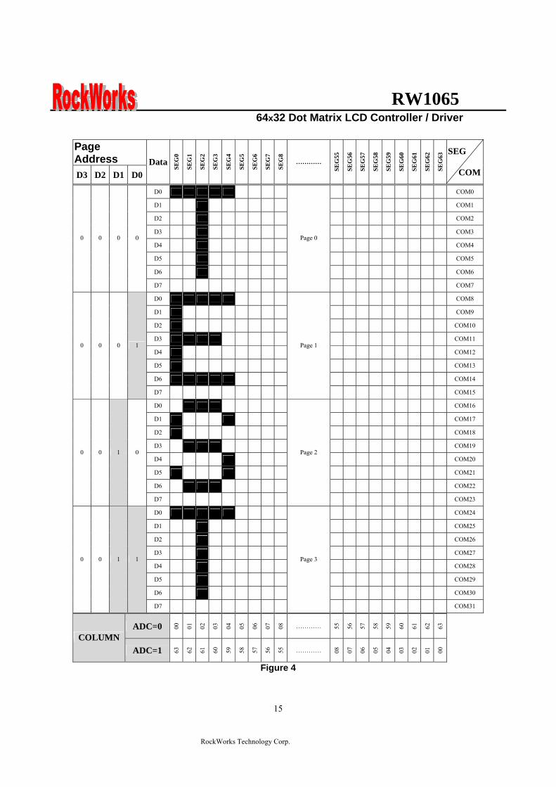
RW1065 64x32 Dot Matrix LCD Controller Driver
RockWorks Technology Corp
15
Figure 4
Page Address D3 D2 D1 D0
DataSE
G0
SEG
1
SEG
2
SEG
3
SEG
4
SEG
5
SEG
6
SEG
7
SEG
8
helliphelliphelliphellip
SEG
55
SEG
56
SEG
57
SEG
58
SEG
59
SEG
60
SEG
61
SEG
62
SEG
63 SEG
COM
D0 COM0
D1 COM1
D2 COM2
D3 COM3
D4 COM4
D5 COM5
D6 COM6
0 0 0 0
D7
Page 0
COM7
D0 COM8
D1 COM9
D2 COM10
D3 COM11
D4 COM12
D5 COM13
D6 COM14
0 0 0 1
D7
Page 1
COM15
D0 COM16
D1 COM17
D2 COM18
D3 COM19
D4 COM20
D5 COM21
D6 COM22
0 0 1 0
D7
Page 2
COM23
D0 COM24
D1 COM25
D2 COM26
D3 COM27
D4 COM28
D5 COM29
D6 COM30
0 0 1 1
D7
Page 3
COM31
ADC=0 00
01
02
03
04
05
06
07
08
helliphelliphelliphellip 55
56
57
58
59
60
61
62
63
COLUMN ADC=1 63
62
61
60
59
58
57
56
55
helliphelliphelliphellip 08
07
06
05
04
03
02
01
00
RW1065 64x32 Dot Matrix LCD Controller Driver
RockWorks Technology Corp
16
Common Timing Generator Circuit Display Data Latch Circuit Generates common timing signals and FR frame signals from the CL basic clock The 132 or 164 duty (for RW1065) can be selected by the Duty Select command The 132 and 164 duties are provided by two chips consisting of the master and slave chips in the common multi-chip mode
This latch stores one line of display data for use by the LCD driver interface circuitry The output of this latch is controlled by the Display ONOFF
132 duty
164 duty
SHL=0
SHL=1
SHL=0
SHL=1
RW1065 64x32 Dot Matrix LCD Controller Driver
RockWorks Technology Corp
17
Display Timing Generator Circuit
The display timing generator circuit generates the timing signal to the line address circuit and the display data latch circuit using the display clock The display data is latched into the display data latch circuit synchronized with the display clock and is output to the data driver output terminal Reading to the display data liquid crystal driver circuits is completely independent of accesses to the display data RAM by the MPU Consequently even if the display data
RAM is accessed asynchronously during liquid crystal display there is absolutely no adverse effect (such asflickering) on the display Moreover the display timing generator circuit generates the common timing and the liquid crystal alternating current signal (FR) from the display clock It generates a drive wave form using a 2 frame alternating current drive method as is shown in Figure 5 for the liquid crystal drive circuit
Two-frame alternating current drive waveform
Figure 5
When multiple RW1065 Series chips are used the slave chip must be supplied the display timing signals(FR CL) from the master chip
Table 5 shows the status of the FR and CL signals
Table 5 Operating Mode FR CL
Master (MS = ldquoHrdquo) The internal oscillator circuit is enabled (CLS = ldquoHrdquo) The internal oscillator circuit is disabled (CLS = ldquoLrdquo)
Output Output
Output Input
Slave (MS = ldquoLrdquo) The internal oscillator circuit is enabled (CLS = ldquoHrdquo) The internal oscillator circuit is disabled (CLS = ldquoLrdquo)
Input Input
Input Input
RW1065 64x32 Dot Matrix LCD Controller Driver
RockWorks Technology Corp
18
The Liquid Crystal Driver Circuits
These are a 64-channel (RW1065) that generate four voltage levels for driving the liquid crystal The combination of the display data the COM scan signal and the FR signal
produces the liquid crystal drive voltage output Figure 6 shows examples of the SEG and COM output waveform
Figure 6
RW1065 64x32 Dot Matrix LCD Controller Driver
RockWorks Technology Corp
19
The Power Supply Circuit
The power supply circuits are low-power consumption power supply circuits that generate the voltage levels required for the liquid crystal drivers They comprise Booster circuits and voltage follower circuits They are only enabled in master operation The power supply circuits can turn on automatically after power on
Consequently it is possible to make an external power supply and the internal power supply function somewhat in parallel
The Liquid Crystal Voltage Generator Circuit The V0 voltage is produced by a resistive voltage divider outside the IC through VRAB pin and can be produced at the V1 V2 V3 and V4 voltage levels required for liquid crystal driving Moreover when the voltage follower changes the impedance it provides V1 V2 V3 and V4 to the liquid crystal drive circuit 15 bias or 16 bias or 18 bias or 19 bias for RW1065 can be selected by BS0 and BS1 pins V0-Vss maximum voltage is 15V Vout-Vss maximum voltage is 17V If VDD lt 35V it can use the Booster circuit 2x3x4xThe booster voltage can follow the spec condition (Vout-Vss ≦ 17V max voltage) if VDD gt35V only use the 2X3X booster circuit that can ensure the V0-Vss voltage ≦ 15V If use the VDD voltage 5V and 4X booster itrsquos over the spec operation condition To turn on built-in power (boosterfollower) must waiting 200mS to display on for boosterfollower stable Therefore power off must follower ldquopower off sequencerdquo too
Power on Display off
Power off
Power off sequence
Wait time gt200mS
Display on
Power on sequence
RW1065 64x32 Dot Matrix LCD Controller Driver
RockWorks Technology Corp
20
The Reset Circuit
When the RTP input comes to the ldquoLrdquo level these LSIs return to the default state Their default states are as follows 1 Display OFF 2 Display all point on is select to normal 3 Display normalreverse is select to normal 4 164 duty is selected 5 Read modify write OFF 6 Column address set to Address 0 7 Page address set to Page 0 8 Start line set to first line 9 Frame frequency set to default 10 Power save mode released 11 Ext set to ldquo0rdquo When the power is turned on the IC internal state becomes unstable and it is necessary to initialize it using the RSTP terminal After the initialization each input terminal should be controlled normally While RSTP is ldquoLrdquo the oscillator works but the display timing generator stops and the CL FR terminals are fixed to ldquoHrdquo The terminals D0 to D7 are not affected
RW1065 64x32 Dot Matrix LCD Controller Driver
RockWorks Technology Corp
21
TABLE OF RW1065 INSTRUCTIONS
Instruction code Instruction RS RW DB7 DB6 DB5 DB4 DB3 DB2 DB1 DB0 Description
EXT=0 or 1
MODE SET 0 0 0 0 0 0 1 1 0 EXT Set EXT mode
Instruction code Instruction RS RW DB7 DB6 DB5 DB4 DB3 DB2 DB1 DB0 Description
EXT=0 Display ONOFF 0 0 0 0 1 1 1 1 1 D D=0Display OFF
D=1Display ONSet page address 0 0 1 0 1 1 1 P2 P1 P0 Set page address
Set column address 0 0 0 1 Y5 Y4 Y3 Y2 Y1 Y0 Set column
address MSB
Read Status 0 1 BUSY 0 ON OFF RESET 0 0 0 0 Read register
status Write display
data 1 0 Write data Write data into DDRAM
Read display data 1 1 Read data Read data from
DDRAM Set initial
display line register
0 0 1 1 S5 S4 S3 S2 S1 S0 Specify the initial
display line to realize vertical scrolling
Instruction code Instruction RS RW DB7 DB6 DB5 DB4 DB3 DB2 DB1 DB0 Description
EXT=1
NOP 0 0 0 0 0 0 0 0 0 0 no operation
Set modiy-read 0 0 0 0 0 0 1 0 0 0 Set modiy-read
mode
END 0 0 0 0 0 0 1 1 1 0 release modiy-read mode
Set power save mode 0 0 0 0 0 0 0 0 1 PSAVE P=0 normal mode
P=1 sleep mode
0 0 0 0 0 1 0 1 Display
COMMAND (double
command)
0 0 FRSEL
0 0 0 0 REV ALLON DUTY
DUTY=1 64 duty DUTY=0 32 duty ALLON=1display all on ALLON=0display
normal REV=1display reverse REV=0display normal FRSEL=1FR frequency double default FRSEL=0FR frequency default
RW1065 64x32 Dot Matrix LCD Controller Driver
RockWorks Technology Corp
22
Command Description
See the Table of RW1065 instructions The RW1065 series identifies a data bus using a combination of RS E and RW signals As the MPU translates a command in the internal timing only (independent from the external clock) its speed is very high The busy check is usually not required
Display ONOFF
EXT RS RW D7 D6 D5 D4 D3 D2 D1 D0
0 0 0 0 0 1 1 1 1 1 D
This command turns the display on and off D=1 Display ON D=0 Display OFF(default)
Set page Address This command specifies the page address that corresponds to the low address of the display data RAM when it is accessed by the MPU Any bit of the display data RAM can be accessed when its page address and column address are specified The display status is not changed even when the page address is changed
EXT RS RW D7 D6 D5 D4 D3 D2 D1 D0
0 0 0 1 0 1 1 1 A2 A1 A0
This command loads the page address register
A2 A1 A0 Page
0 0 0 0 (default)
0 0 1 1 0 1 0 2 0 1 1 3 1 0 0 4 1 0 1 5 1 1 0 6 1 1 1 7
Page mapping see Figure 4
RW1065 64x32 Dot Matrix LCD Controller Driver
RockWorks Technology Corp
23
Set Column Address This command specifies a column address of the display data RAM When the display data RAM is accessed by the MPU continuously the column address is incremented by I each time it is accessed from the set address Therefore the MPU can access to data continuously The column address stops to be incremented at address 63 and the page address is not changed continuously
EXT RS RW D7 D6 D5 D4 D3 D2 D1 D0
0 0 0 0 1 A5 A4 A3 A2 A1 A0
A5 A4 A3 A2 A1 A0 Column Address0 0 0 0 0 0 0(default) 0 0 0 0 0 1 1
1 1 1 1 1 1 63
Read Status
EXT RS RW D7 D6 D5 D4 D3 D2 D1 D0
0 0 1 BUSY 0 ON OFF RESET 0 0 0 0
The BUSY Flag bit indicates that RW 1065 is operating or no operating
BUSY=1 Operation BUSY=0 Ready
The ONOFF bit indicates the current status of the display It is the inverse of the polarity of the display ONOFF command ONOFF=1 Display OFF ONOFF=0 Display ON The RESET bit indicates whether the driver is executing a hardware or software reset or if it is in normal operating mode RESET=1 Currently executing reset command RESET=0 Normal operation
RW1065 64x32 Dot Matrix LCD Controller Driver
RockWorks Technology Corp
24
Write Display Data
EXT RS RW D7 D6 D5 D4 D3 D2 D1 D0
0 1 0 Write data
Writes 8-bits of data into the display data RAM at a location specified by the contents of the column address and page address registers and then increments the column address register by one
Read Display Data
EXT RS RW D7 D6 D5 D4 D3 D2 D1 D0
0 1 1 Read data
Reads 8-bits of data from the data IO latch updates the contents of the IO latch with display data from the display data RAM location specified by the contents of the column address and page address registers and then increments the column address register After loading a new address into the column address register one dummy read is required before valid data is obtained
Set initial display line register
EXT RS RW D7 D6 D5 D4 D3 D2 D1 D0
0 0 0 1 1 S5 S4 S3 S2 S1 S0
Loads the RAM line address of the initial display line COM 0 into the initial display line register The RAM display data becomes the top line of the LCD screen It is followed by the higher number lines in ascending order corresponding to the duty cycle The screen can be scrolled using this command by incrementing the line address(default value=rdquo00Hrdquo)
RW1065 64x32 Dot Matrix LCD Controller Driver
RockWorks Technology Corp
25
Read-Modify-Write
EXT RS RW D7 D6 D5 D4 D3 D2 D1 D0
1 0 0 0 0 0 0 1 0 0 0
This command defeats column address register auto-increment after data reads The current contents of the column Address register are saved The mode remains active until an End command is received When the End command is entered the column address is returned to the one used during input of Read-Modify-Write Command This function can reduce the load of MPU when data change is repeated as a specific display area Any command other than Data Read or Write can be used in the Read-Modify-Write mode However the Column Address Set command cannot be used
End
EXT RS RW D7 D6 D5 D4 D3 D2 D1 D0
1 0 0 0 0 0 0 1 1 1 0
This command cancels read-modify-write mode and restores the contents of the column address register to their value prior to the receipt of the Read-Modify-Write command
N N+1 N+2 N+3 N+m N
Read -modify-write mode set End
Returm
Column address
Set page address
Set column address
Read-modify-write
Dummy read
Read data
Write data
End
CompletedNo
Yes
RW1065 64x32 Dot Matrix LCD Controller Driver
RockWorks Technology Corp
26
Set power save mode
EXT RS RW D7 D6 D5 D4 D3 D2 D1 D0
1 0 0 0 0 0 0 0 0 1 PSAVE
When power save mode is entered thus greatly reducing power consumption In the power save mode the display data is saved as is the operating mode that was in effect before the power saver mode was initiated and the MPU is still able to access the display data RAM PSAVE=1 Sleep mode PSAVE=0 Normal mode Sleep mode This stops all operations in the LCD display system and as long as there are no accesses from the MPU the consumption current is reduced to a value near the static current The internal modes during sleep mode are as follows 1 The oscillator circuit and the LCD power supply circuit are halted 2 All liquid crystal drive circuits are halted and the segment and common drive outputs output a Vss level
Display command double command
EXT RS RW D7 D6 D5 D4 D3 D2 D1 D0
1 0 0 0 0 0 0 0 1 0 1
1 0 0 FRSEL 0 0 0 0 REV ALLON DUTY
Display NormalReverse set REV=1 Reverse REV=0 Normal(default) Display All Point ONOFF ALLON=1 All display points ON ALLON=0 Normal(default) Select Duty Duty=1 164 duty cycle(default) Duty=0 132 duty cycle FRAME FREQUENCY Select FRSEL=1 Double FRSEL=0 (default)
RW1065 64x32 Dot Matrix LCD Controller Driver
RockWorks Technology Corp
27
Hardware Pin Set
Select ADC by ADC Pin The pin selects the relationship between display data RAM column addresses and segment drivers ADC=1 SEG0larrcolumn address 3FHhellipinverted ADC=0 SEG0larrcolumn address 00Hhellipnormal(default) This command is provided to reduce restrictions on the placement of driver ICs and routing of traces during printed circuit Board design See Figure 4 for a table of segments and column addresses for the two values of D
Select SHL by SHL Pin The pin selects the com output scan direction SHL=1 Reverse directioncom63rarrcom0 SHL=0 Normal com0rarrcom63 Both master and slave should set identical SHL value
Select LCD Bias by BS0 BS1 Pin
BS1 BS0 Bias 0 0 15 bias 0 1 16 bias 1 0 18 bias 1 1 19 bias
RW1065 64x32 Dot Matrix LCD Controller Driver
RockWorks Technology Corp
28
When an External Resistance is Used The liquid crystal power supply voltage V0 is set by adding resistors Rarsquo and Rbrsquo between VDD and VR and between VR and V0 respectively
RW1065
RW1065 64x32 Dot Matrix LCD Controller Driver
RockWorks Technology Corp
29
The set voltage circuits
Using the step-up voltage circuits equipped within the RW1065 chips it is possible to produce a 2X 3X 4X step-up voltage levels 2X step-up
To produce voltage level in the positive direction at the Vout terminal that is 2 times the voltage difference between VSS and VDD2 Please configure set voltage circuits like this Place a 1uF~22uF capacitor between CAP1N and CAP1P Place a 1uF~22uF capacitor between VSS and VOUT Short CAP2P CAP3P and VOUT Leave CAP2N open 3X step-up
To produce voltage level in the positive direction at the Vout terminal that is 3 times the voltage difference between VSS and VDD2 Please configure set voltage circuits like this Place a 1uF~22uF capacitor between CAP1N and CAP1P Place a 1uF~22uF capacitor between VSS and VOUT Place a 1uF~22uF capacitor and 100 ohms resistor between CAP2N and CAP2P Short CAP3P and Vout 4X step-up
To produce voltage level in the positive direction at the Vout terminal that is 4 times the voltage difference between VSS and VDD2 Please configure set voltage circuits like this Place a 1uF~22uF capacitor between CAP1N and CAP1P Place a 1uF~22uF capacitor between VSS and VOUT Place a 1uF~22uF capacitor and 100 ohms resistor between CAP2N and CAP2P Place a 1uF~22uF capacitor and 100 ohms resistor between CAP1N and CAP3P
RW1065 64x32 Dot Matrix LCD Controller Driver
RockWorks Technology Corp
30
ABSOLUTE MAXIMUM RATINGS Characteristics Symbol Value Unit
Power supply voltage VDD -03 to +70 V
LCD driver voltage Vout 0 to +17 V
Input voltage VIN -03 to VDD+03 V
Operating temperature TA -40 to +85
Storage temperature TSTO -55 to +125
DC CHARACTERISTICS
Rating Item Symbol Condition Min Typ Max Unit ApplicablePin
Operating Voltage VDD - 27 30 55 V VDD1
Step up output voltage Vout (Relative to VDD) 0 - 17 V Vout
Voltage follower circuit operating Voltage V0 (Relative to VDD) 0 - 15 V V0
V0 accuracy V0 - 0 - 15 V0
High-level Input Voltage Low-level Input Voltage
VIHC VILC - 07 VDD
Vss - VDD 09 V 2
High-level Output Voltage Low-level Output Voltage
VOHC VOLC
IOH = ndash05 mA IOL = 05 mA
08VDD Vss - VDD
02 VDD V 3
Input leakage current ILI VIN = VDD or VSS -1 - 2 uA 4
Output leakage current ILO - -1 1 uA 5
Liquid Crystal Driver ON Resistance RON
Ta= 25degC(Relative To VDD)
V0 =15 V - 16 20 KΩ SEGn COMn 6
Internal Oscillator fOSC 2286 254 2794 Oscillator
Frequency External Input RECOMMAND fCL
Ta = 25degC 132Duty 2286 254 2794
kHz CL
Internal Oscillator fOSC 45 5 55 Oscillator
Frequency External Input RECOMMAND fCL
Ta = 25degC 164Duty 45 5 55
kHz CL
bullDynamic Consumption Current During Display with the Internal Power Supply OFF Current consumed by total ICs when an external power supply is used
Unless otherwise specified Vss=0V VDD=30V
RW1065 64x32 Dot Matrix LCD Controller Driver
RockWorks Technology Corp
31
Display Pattern OFF
Ta = 25degC Vout=17V Rating Item Symbol Condition Min Typ Max Unit Notes
VDD=30 V V0-Vss=8V - 10 15 RW1065 IDD VDD=50 V V0-Vss=8V - 35 45
microA 7
Display Pattern Checker
Ta = 25degC Vout=17V Rating Item Symbol Condition Min Typ Max Unit Notes
VDD=30 V V0-Vss=8V - 15 20 RW1065 IDD VDD=50 V V0-Vss=8V - 40 50
microA 7
Display Pattern OFF
Ta = 25degC Vout=17V Rating Item Symbol Condition Min Typ Max Unit Notes
VDD=30 V V0-Vss=8V - 15 20 RW1065 IDD VDD=50 V V0-Vss=8V - 40 50
microA 7
Display pattern Checker
Ta = 25degC Vout=17V Rating Item Symbol Condition Min Typ Max Unit Notes
VDD=30 V V0-Vss=8V - 65 80 RW1065 IDD VDD=50 V V0-Vss=8V - 130 150
microA 7
bull Consumption Current at Time of Power Saver Mode VSS = 0 V VDD = 30 V plusmn 10
Rating Item Symbol Condition Min Typ Max Unit Notes
Sleep mode IDD - - 5 10 microA -
References for items market with 1 While a broad range of operating voltages is guaranteed performance cannot be guaranteed if there are sudden fluctuations to the
voltage while the MPU is being accessed 2 The RS D0 to D5 D6 D7 E RW CS1BP CS2P CLS CL FR MS and RST
― terminals
3 The D0 to D7 FR and CL terminals 4 The RS E RW CS1BP CS2P CLS MS and RST
― terminals
5 Applies when the D0 to D5 D6 D7 CL and FR terminals are in a high impedance state 6 These are the resistance values for when a 01 V voltage is applied between the output terminals SEGn or COMn and
the various power supply terminals (V1 V2 V3 and V4) These are specified for the operating voltage (3) range RON = 01 V ∆I (Where ∆I is the current that flows when 01 V is applied while the power supply is ON)
7 It indicates the current consumed on ICs alone when the internal oscillator circuit and display are turned on Does not include the current due to the LCD panel capacity and wiring capacity Applicable only when there is no access from the MPU
RW1065 64x32 Dot Matrix LCD Controller Driver
RockWorks Technology Corp
32
TIMING CHARACTERISTICS
68 Interface
(Ta=-40 to 85 degC) VDD=27 to 45V
Rating VDD=45 to 55V
Rating Item Signal Symbol ConditionMin Max Min Max
Units
Address hold time RS tAH6 0 mdash 0 mdash Address setup time RS tAW6
mdash 0 mdash 0 mdash
ns
System cycle time RS tCYC6 mdash 900 mdash 800 mdash ns Data setup time D0 to D7 tDS6 100 mdash 100 mdash Data hold time D0 to D7 tDH6
mdash 0 mdash 0 mdash
ns
Access time D0 to D7 tACC6 mdash 350 mdash 250
Output disable time D0 to D7 tOH6 CL = 100 pF
mdash 300 mdash 200 ns
Read tEWHR 360 mdash 300 mdash Enable H pulse time
WriteE
tEWHW mdash
360 mdash 300 mdash ns
Read tEWLR 450 mdash 400 mdash Enable L pulse time
WriteE
tEWLW mdash
450 mdash 400 mdash ns
1 All timing is specified using 20 and 80 of VDD as the reference 2 tEWLW and tEWLR are specified as the overlap between CS1BP being ldquoLrdquo (CS2P = ldquoHrdquo) and E
RW1065 64x32 Dot Matrix LCD Controller Driver
RockWorks Technology Corp
33
Reset Timing
Rating Item Signal Symbol Condition
Min Typ Max Units
Reset time mdash tR mdash mdash - 2 micros
Reset ldquoLrdquo pulse width RST tRW mdash 2 - mdash micros
1 When double chip was be used then the duty set command must be set between the tR
RW1065 64x32 Dot Matrix LCD Controller Driver
RockWorks Technology Corp
34
IO PAD CONFIGURATION
RW1065 64x32 Dot Matrix LCD Controller Driver
RockWorks Technology Corp
35
THE MPU INTERFACE (REFERENCE EXAMPLES) The RW1065 Series can be connected to 6800 Series MPUs The display area can be enlarged by using multiple RW1065 Series chips When this is done the chip select signal can be used to select the individual ICs to access
6800 Series MPUs
RW
106
5
RW1065 64x32 Dot Matrix LCD Controller Driver
RockWorks Technology Corp
36
When using external multi-level power supply for LCD driving (REFERENCE EXAMPLE)
Using a resistor divider can provide RW1065 external multi-level power supply for LCD driving
The circuit below shows a resistor divider network which can bias V0 V1 V2 V3 and V4 externally
RW1065 64x32 Dot Matrix LCD Controller Driver
RockWorks Technology Corp
37
bullWhen V0 V1 V2 V3 and V4 are biased by external power supply analog section of RW1065 should be turn off by software during LCD initialization The example in below shows the sequence to turn off analog section when external bias is used Begin of LCD initialization 1 Reset RW1065 2 SET EXT=1 (mode instruction)
RS RW DB7 DB6 DB5 DB4 DB3 DB2 DB1 DB00 0 0 0 0 0 1 1 0 1
3 SET Display Command (double command)
RS RW DB7 DB6 DB5 DB4 DB3 DB2 DB1 DB00 0 0 0 0 0 0 1 0 1 0 0 0 0 1 1 0 0 0 1
4 SET EXT=1 (mode instruction)
RS RW DB7 DB6 DB5 DB4 DB3 DB2 DB1 DB00 0 0 0 0 0 1 1 0 0
End of LCD initialization
bullBecause pins can not set LCD bias when external power supplies are used for LCD driving the bias can be set by an appropriate configuration for a resistor voltage divider networks The example is shown below
VSS
R
R
NR
R
R
RV1
RV2
RV3
RV4
V0
Bias Network Circuit Concept 15 Bias N=1 total = 5R 16 Bias N=2 total =6R 18 Bias N=4 total =8R 19 Bias N=5 total = 9R
RW1065 64x32 Dot Matrix LCD Controller Driver
RockWorks Technology Corp
38
Single chip solution for RW1065 application (REFERENCE EXAMPLE)
For a 64x32 application the duty cycle of LCD panel is 164 and the display duty of RW1065 should be set to 164 The display duty cycle can be selected by the DUTY bit in display command The diagram for 64x32 application is shown below
64 SEGx32COM LCD Panel
164 duty cycle
RW1065 DUTY=1
COM1~33
SEG1~65
RW1065 64x32 Dot Matrix LCD Controller Driver
RockWorks Technology Corp
39
Using an adjustable resistor on the main board to adjust the contrast of liquid crystal display (REFERENCE EXAMPLE)
The schematic shows an adjustable resistor on main board that can adjust voltage level of V0
RW1065 64x32 Dot Matrix LCD Controller Driver
RockWorks Technology Corp
40
Package information (Please pay close attention to the information in this section Do not hesitate to consult with our sale representative if you have any question or concern)
In order to make better bonding yield for RW1065 please follow the tips and recommendations in this section In this section few tips about COB footprint style PCB layout and wire bonding will be discussed
The drawing in below shows the PCB footprint style which we recommend for RW1065 Pads array in
curve shape is easier for Al wire bonding Besides that a real size COB footprint for RW1065 is also shown in below RW1065 COB footprint is also available in powerpcb or protel format for design reference purpose
The ratio is 11
RW1065 64x32 Dot Matrix LCD Controller Driver
RockWorks Technology Corp
41
During COB footprint design there have some tips about footprint that the PCB designer should know The angle between bonding wire and vertical line should less than 45 Otherwise the wire shorts would become very easy to happen at fours corners of the chip
The angle between bonding wire and vertical line could be reduced by expanding the distance between pads array and the chip In addition reducing length in horizon direction of pads array could minimize the angle between bonding wire and vertical line The picture in below will help to illustrate this concept From the experiences COB footprint style affects the bonding yield
Bad Wires are too close to each other
The angle between bonding wire and vertical line is greater than 45
The angle between bonding wire and vertical line is less than 45
Wires are not too close to each other
Reducing length in horizon direction of pads array could minimize the angle between bonding wire and vertical line
The angle between bonding wire and vertical line could be reduced by expanding the distance between pads array and the chip
RW1065 64x32 Dot Matrix LCD Controller Driver
RockWorks Technology Corp
42
If the gap between pads of COB footprint is filled with solder mask coating it is difficult to bond Al wire to
the pads The top solder masks layer that overlap COB footprint area should be removed
Please use 1 mils diameter Al wire for RW1065 wire bonding
1 2 3 4 5 6
A
B
C
D
654321
D
C
B
A
Title
Number RevisionSize
C
Date 29-Aug-2007 Sheet of File D公司資料99seMyDesignddb Drawn By
RW1065
COM131
COM142
COM153
COM164
COM175
COM186
COM197
COM208
COM219
COM2210
COM2311
COM2412
COM2513
COM2614
COM2715
COM2816
COM2917
COM3018
COM3119
SEG
6320
SEG
6221
SEG
6122
SEG
6023
SEG
5924
SEG
5825
SEG
5726
SEG
5627
SEG
5528
SEG
5429
SEG
5330
SEG
5231
SEG
5132
SEG
5033
SEG
4934
SEG
4835
SEG
4736
SEG
4637
SEG
4538
SEG
4439
SEG
4340
SEG
4241
SEG
4142
SEG
4043
SEG
3944
SEG
3845
SEG
3746
SEG
3647
SEG
3548
SEG
3449
SEG
3350
SEG
3251
SEG
3152
SEG
3053
SEG
2954
SEG
2855
SEG
2756
SEG
2657
SEG
2558
SEG
2459
SEG
2360
SEG
2261
SEG
2162
SEG
2063
SEG
1964
SEG
1865
SEG
1766
SEG
1667
SEG
1568
SEG
1469
SEG13 70SEG12 71SEG11 72SEG10 73SEG9 74SEG8 75SEG7 76SEG6 77SEG5 78SEG4 79SEG3 80SEG2 81SEG1 82SEG0 83ADCP 84CLL 85
VSS
86D
087
D1
88D
289
D3
90D
491
D5
92D
693
D7
94C
S1B
P95
CS2
P96
ERD
P97
AO
P(R
S)98
RW
RP
99V
DD
100
RST
P10
1C
LSP
102
FRR
103
MSP
104
BS1
P10
5B
S0P
106
SHLP
107
VD
D2
108
CA
P2N
109
CA
P2P
110
CA
P1P
111
CA
P1N
112
CA
P3P
113
VO
UT
114
V0
115
VR
AB
116
V3
117
V2
118
V4
119
V1
120
CO
M0
121
CO
M1
122
CO
M2
123
CO
M3
124
CO
M4
125
CO
M5
126
CO
M6
127
CO
M7
128
CO
M8
129
CO
M9
130
CO
M10
131
CO
M11
132
CO
M12
133
4897x1902 um
IC1
RW1065
C9CAPR4
100R0603
R30R0603
C8
CAP
C7
CAP
R2
100R0603
R1
0R0603C6 22uf
R50R
R6300R
R7RES1
R8NC R9
100R0603
VDD
R10
NC
R11
100R0603
R12
100R0603
R13
NC
R14
100R0603
R15
NC
VDD
D0
D1
D2
D3
D4
D5
D6
D7
DB[07]
VDDC5
01uf0603
VD
D
CS2
P
123456789
1011121314151617181920
J1
CON20
C1201uf0603
R3951K0603
VDD
CAP Value1UF~22UF
2XPut C6C8 Short R1R3Open R2R4C7C93XPut C6C8C9 R4Short R1Open R2R3C74XOpen R1R3
BS0 BS1 Bias0 0
0 1
1 0
11
15 bias
16 bias
18 bias
19 bias
ADC=0 SEG0lt~column address 00Hnormal(default) ADC=1 SEG0lt~column address 3FHinverted
SHL=0 Normal COM0~gtCOM63(default)SHL=1 Reverse direction COM63~gtCOM0
R16100R0603
LCD PANEL 64X32RockWorks
RW1065 64X32
COM0-31 SEG0-63SHL=0 ADC=0
SHL=1COM31-0
ADC=1SEG63-0
if use single chip for 32 command displaythe display command must select 164 dutyDisplay panel must select 164 duty type
VO
UT
C3P
C1N
C1P
C2P
C2N
VDD2
ADC
SHL
BS0
BS1
CLLADC
V1
V2
V3
V4
VR
AB
V0
VO
UT
C3P
C1N
C1P
C2P
C2N
VD
D2
SHL
BS0
BS1
FRR
RST
P
RW
RS
E CS1
B
CS1
V0RSRWED0D1D2D3D4D5D6D7
RSTPAK
C4
22uf
RBRES1
RA1RES1
C2
22uf
C1
22uf
C3
22uf
C0
22uf
R20
100k0603
R21
100k0603
R17
200K0603
V1
V2
V3
V4 VRAB
V0
V0
OPTION
B
R18
300R0603
RA2RES1
VADJ
R19100R
R23 RES1R22 0R
R24
RES1
R25
0R
VDD
CS1BP
CS2P
CS1
CS1
R26
22R0603
R27
22R0603
C1047uf
C11
01uf
VSS_INVDD_IN
D1DIODE
FGND
鐵框地
VSS
VDD
R28 10RR29 10RR30 10RR31 10RR32 10RR33 10RR34 10RR35 10RR36 10RR37 10RR38 10R
VADJ
1 2 3 4 5 6
A
B
C
D
654321
D
C
B
A
Title
Number RevisionSize
C
Date 29-Aug-2007 Sheet of File D公司資料99seMyDesignddb Drawn By
RW1065
COM131
COM142
COM153
COM164
COM175
COM186
COM197
COM208
COM219
COM2210
COM2311
COM2412
COM2513
COM2614
COM2715
COM2816
COM2917
COM3018
COM3119
SEG
6320
SEG
6221
SEG
6122
SEG
6023
SEG
5924
SEG
5825
SEG
5726
SEG
5627
SEG
5528
SEG
5429
SEG
5330
SEG
5231
SEG
5132
SEG
5033
SEG
4934
SEG
4835
SEG
4736
SEG
4637
SEG
4538
SEG
4439
SEG
4340
SEG
4241
SEG
4142
SEG
4043
SEG
3944
SEG
3845
SEG
3746
SEG
3647
SEG
3548
SEG
3449
SEG
3350
SEG
3251
SEG
3152
SEG
3053
SEG
2954
SEG
2855
SEG
2756
SEG
2657
SEG
2558
SEG
2459
SEG
2360
SEG
2261
SEG
2162
SEG
2063
SEG
1964
SEG
1865
SEG
1766
SEG
1667
SEG
1568
SEG
1469
SEG13 70SEG12 71SEG11 72SEG10 73SEG9 74SEG8 75SEG7 76SEG6 77SEG5 78SEG4 79SEG3 80SEG2 81SEG1 82SEG0 83ADCP 84CLL 85
VSS
86D
087
D1
88D
289
D3
90D
491
D5
92D
693
D7
94C
S1B
P95
CS2
P96
ERD
P97
AO
P(R
S)98
RW
RP
99V
DD
100
RST
P10
1C
LSP
102
FRR
103
MSP
104
BS1
P10
5B
S0P
106
SHLP
107
VD
D2
108
CA
P2N
109
CA
P2P
110
CA
P1P
111
CA
P1N
112
CA
P3P
113
VO
UT
114
V0
115
VR
AB
116
V3
117
V2
118
V4
119
V1
120
CO
M0
121
CO
M1
122
CO
M2
123
CO
M3
124
CO
M4
125
CO
M5
126
CO
M6
127
CO
M7
128
CO
M8
129
CO
M9
130
CO
M10
131
CO
M11
132
CO
M12
133
4897x1902 um
IC1
RW1065 Master
RW1065
COM131
COM142
COM153
COM164
COM175
COM186
COM197
COM208
COM219
COM2210
COM2311
COM2412
COM2513
COM2614
COM2715
COM2816
COM2917
COM3018
COM3119
SEG
6320
SEG
6221
SEG
6122
SEG
6023
SEG
5924
SEG
5825
SEG
5726
SEG
5627
SEG
5528
SEG
5429
SEG
5330
SEG
5231
SEG
5132
SEG
5033
SEG
4934
SEG
4835
SEG
4736
SEG
4637
SEG
4538
SEG
4439
SEG
4340
SEG
4241
SEG
4142
SEG
4043
SEG
3944
SEG
3845
SEG
3746
SEG
3647
SEG
3548
SEG
3449
SEG
3350
SEG
3251
SEG
3152
SEG
3053
SEG
2954
SEG
2855
SEG
2756
SEG
2657
SEG
2558
SEG
2459
SEG
2360
SEG
2261
SEG
2162
SEG
2063
SEG
1964
SEG
1865
SEG
1766
SEG
1667
SEG
1568
SEG
1469
SEG13 70SEG12 71SEG11 72SEG10 73SEG9 74SEG8 75SEG7 76SEG6 77SEG5 78SEG4 79SEG3 80SEG2 81SEG1 82SEG0 83ADCP 84CLL 85
VSS
86D
087
D1
88D
289
D3
90D
491
D5
92D
693
D7
94C
S1B
P95
CS2
P96
ERD
P97
AO
P(R
S)98
RW
RP
99V
DD
100
RST
P10
1C
LSP
102
FRR
103
MSP
104
BS1
P10
5B
S0P
106
SHLP
107
VD
D2
108
CA
P2N
109
CA
P2P
110
CA
P1P
111
CA
P1N
112
CA
P3P
113
VO
UT
114
V0
115
VR
AB
116
V3
117
V2
118
V4
119
V1
120
CO
M0
121
CO
M1
122
CO
M2
123
CO
M3
124
CO
M4
125
CO
M5
126
CO
M6
127
CO
M7
128
CO
M8
129
CO
M9
130
CO
M10
131
CO
M11
132
CO
M12
133
4897x1902 um
IC2
RW1065 Slave
C4
22uf
RBRES1
RA1RES1
C2
22uf
C1
22uf
C3
22uf
C0
22ufC9CAPR4
100R0603
R30R0603
C8
CAP
C7
CAP
R2
100R0603
R1
0R0603C6 22uf
R50R0603
R6300R0603
R7RES1
R8NC R9
100R0603
VDD
R10
NC
R11
100R0603
R12
NC
R13
100R0603
R14
100R0603
R15
NC
R16
100R0603
R17
NC
VDD
D0
D1
D2
D3
D4
D5
D6
D7
D0
D1
D2
D3
D4
D5
D6
D7
DB[07] DB[07]
VDDC10
01uf0603
VD
D
IC1_
CS2
P
VDD
IC2_
CS2
P
VD
D
C11
01uf0603
VSS
VSS
LCD PANEL 128X64
Master COM0-31 Slave COM32-63
Master SEG0-63 Slave SEG64-127
123456789
1011121314151617181920
J1
CON20
Master Slave
CAP Value1UF~22UF
2XPut C6C8 Short R1R3Open R2R4C7C93XPut C6C8C9 R4Short R1Open R2R3C74XOpen R1R3
RockWorksRW1065 128x64
BS0 BS1 Bias0 0
0 1
1 0
11
15 bias
16 bias
18 bias
19 bias
ADC=0 SEG0lt~column address 00Hnormal(default) ADC=1 SEG0lt~column address 3FHinverted
SHL=0 Normal COM0~gtCOM63(default)SHL=1 Reverse direction COM63~gtCOM0Both Master and Slave should set identical SHL value
SHL=0 SHL=0
ADC=0 ADC=0
Slave COM31-0
Slave SEG127-64
SHL=1
ADC=1
SHL=1Master COM63-32
ADC=1Master SEG63-0
R18100R0603
R22
100k0603
R23
100k0603
C501uF0603
R4551K0603
VDD
R19
200K0603
ADC1
ADC2
SHL
BS0
BS1
VDD2
V1
V2
V3
V4 VRAB
V0
V0V
OU
T
C3P
C1N
C1P
C2P
C2N
V1
V2
V3
V4
VR
AB
V0
VO
UT
C3P
C1N
C1P
C2P
C2N
VD
D2
SHL
BS0
BS1
FRR
RST
P
RW
RS
E IC1_
CS1
BP
V1
V2
V3
V4
VR
AB
V0
VO
UT
VD
D2
SHL
BS0
BS1
FRR
RST
P
RW
RS
E IC2_
CS1
BP
CLLADC1
CLLADC2
RSTP
CS1CS2
V0RSRWED0D1D2D3D4D5D6D7
AK
OPTION
R20
300R0603
RA2RES1
VADJ
R21
100R
B
R25 RESR24 0R
R26 RES R27 0RVDD
IC1_CS1BP
IC1_CS2P
CS1
CS1
R28 0R R29 RES
R30 RES R31 0R
IC2_CS1BP
IC2_CS2P
CS2
CS2
R32
22R0603
R33
22R0603
C1001uf
C11
47uf
D1DIODE
FGND
鐵框地
VSS
VDD
R34 10RR35 10RR36 10RR37 10RR38 10RR39 10RR40 10RR41 10RR42 10RR43 10RR44 10R
VSS_INVDD_IN
VADJ
VDD
1 2 3 4 5 6 7 8
A
B
C
D
87654321
D
C
B
A
Title
Number RevisionSize
D
Date 29-Aug-2007 Sheet of File D公司資料 99seMyDesignddb Drawn By
C422uf
RBRES1
RA1RES1
C3
22uf
C2
22uf
C1
22uf
C0
22ufC9CAPR4
100R0603
R30R0603
C8
CAP
C7
CAP
R2
100R0603
R1
0R0603C6 22uf
R220R0603
R23300R0603
R24RES1
R39
NCR40
100 ohm0603
VDD
R41
NC
R42
100 ohm0603
R43
NC
R44
100 ohm0603
R45
NC
R46
100 ohm0603
R47
100 ohm0603
R48
NC
R49
100 ohm0603
R50
NC
VDDCAP Value1UF~22UF
2XPut C6C8 Short R1R3Open R2R4C7C93XPut C6C8C9 R4Short R1Open R2R3C74XOpen R1R3
BS0 BS1 Bias0 0
0 1
1 0
11
15 bias
16 bias
18 bias
19 bias
ADC=0 SEG0lt~column address 00Hnormal(default)
ADC=1 SEG0lt~column address 3FHinverted
SHL=0 Normal COM0~gtCOM63(default)SHL=1 Reverse direction COM63~gtCOM0Both Master and Slave should set identical SHL value
R7
100k0603
R8
100k0603
V1
V2
V3
V4
V0
VRAB
V0
R5
200K
VDD2
VO
UT
C3P
C1N
C1P
C2P
C2N
ADC1
ADC2
ADC3
SHL
BS0
BS1
CS1CS2CS3
V0RSRWED0D1D2D3D4D5D6D7
RSTP
R3851K0603
C5
01uF
VDD
OPTION
R6
300R0603R9100R
RA2RES1
VADJ
RW1065
COM131
COM142
COM153
COM164
COM175
COM186
COM197
COM208
COM219
COM2210
COM2311
COM2412
COM2513
COM2614
COM2715
COM2816
COM2917
COM3018
COM3119
SEG
6320
SEG
6221
SEG
6122
SEG
6023
SEG
5924
SEG
5825
SEG
5726
SEG
5627
SEG
5528
SEG
5429
SEG
5330
SEG
5231
SEG
5132
SEG
5033
SEG
4934
SEG
4835
SEG
4736
SEG
4637
SEG
4538
SEG
4439
SEG
4340
SEG
4241
SEG
4142
SEG
4043
SEG
3944
SEG
3845
SEG
3746
SEG
3647
SEG
3548
SEG
3449
SEG
3350
SEG
3251
SEG
3152
SEG
3053
SEG
2954
SEG
2855
SEG
2756
SEG
2657
SEG
2558
SEG
2459
SEG
2360
SEG
2261
SEG
2162
SEG
2063
SEG
1964
SEG
1865
SEG
1766
SEG
1667
SEG
1568
SEG
1469
SEG13 70SEG12 71SEG11 72SEG10 73SEG9 74SEG8 75SEG7 76SEG6 77SEG5 78SEG4 79SEG3 80SEG2 81SEG1 82SEG0 83ADCP 84CLL 85
VSS
86D
087
D1
88D
289
D3
90D
491
D5
92D
693
D7
94C
S1B
P95
CS2
P96
ERD
P97
AO
P(R
S)98
RW
RP
99V
DD
100
RST
P10
1C
LSP
102
FRR
103
MSP
104
BS1
P10
5B
S0P
106
SHLP
107
VD
D2
108
CA
P2N
109
CA
P2P
110
CA
P1P
111
CA
P1N
112
CA
P3P
113
VO
UT
114
V0
115
VR
AB
116
V3
117
V2
118
V4
119
V1
120
CO
M0
121
CO
M1
122
CO
M2
123
CO
M3
124
CO
M4
125
CO
M5
126
CO
M6
127
CO
M7
128
CO
M8
129
CO
M9
130
CO
M10
131
CO
M11
132
CO
M12
133
4897x1902 um
IC1
RW1065 Master
RW1065
COM131
COM142
COM153
COM164
COM175
COM186
COM197
COM208
COM219
COM2210
COM2311
COM2412
COM2513
COM2614
COM2715
COM2816
COM2917
COM3018
COM3119
SEG
6320
SEG
6221
SEG
6122
SEG
6023
SEG
5924
SEG
5825
SEG
5726
SEG
5627
SEG
5528
SEG
5429
SEG
5330
SEG
5231
SEG
5132
SEG
5033
SEG
4934
SEG
4835
SEG
4736
SEG
4637
SEG
4538
SEG
4439
SEG
4340
SEG
4241
SEG
4142
SEG
4043
SEG
3944
SEG
3845
SEG
3746
SEG
3647
SEG
3548
SEG
3449
SEG
3350
SEG
3251
SEG
3152
SEG
3053
SEG
2954
SEG
2855
SEG
2756
SEG
2657
SEG
2558
SEG
2459
SEG
2360
SEG
2261
SEG
2162
SEG
2063
SEG
1964
SEG
1865
SEG
1766
SEG
1667
SEG
1568
SEG
1469
SEG13 70SEG12 71SEG11 72SEG10 73SEG9 74SEG8 75SEG7 76SEG6 77SEG5 78SEG4 79SEG3 80SEG2 81SEG1 82SEG0 83ADCP 84CLL 85
VSS
86D
087
D1
88D
289
D3
90D
491
D5
92D
693
D7
94C
S1B
P95
CS2
P96
ERD
P97
AO
P(R
S)98
RW
RP
99V
DD
100
RST
P10
1C
LSP
102
FRR
103
MSP
104
BS1
P10
5B
S0P
106
SHLP
107
VD
D2
108
CA
P2N
109
CA
P2P
110
CA
P1P
111
CA
P1N
112
CA
P3P
113
VO
UT
114
V0
115
VR
AB
116
V3
117
V2
118
V4
119
V1
120
CO
M0
121
CO
M1
122
CO
M2
123
CO
M3
124
CO
M4
125
CO
M5
126
CO
M6
127
CO
M7
128
CO
M8
129
CO
M9
130
CO
M10
131
CO
M11
132
CO
M12
133
4897x1902 um
IC2
RW1065 Slave
D0
D1
D2
D3
D4
D5
D6
D7
D0
D1
D2
D3
D4
D5
D6
D7
DB[07] DB[07]
VDDC8
01uf0603
VD
D
VDD
VD
D
C9
01uf0603
VSS
VSS
LCD PANEL 192X64
Master COM0-31 Slave COM32-63
Master SEG0-63 Slave SEG64-127
Master Slave
RockWorksRW1065 192x64
RW1065
COM131
COM142
COM153
COM164
COM175
COM186
COM197
COM208
COM219
COM2210
COM2311
COM2412
COM2513
COM2614
COM2715
COM2816
COM2917
COM3018
COM3119
SEG
6320
SEG
6221
SEG
6122
SEG
6023
SEG
5924
SEG
5825
SEG
5726
SEG
5627
SEG
5528
SEG
5429
SEG
5330
SEG
5231
SEG
5132
SEG
5033
SEG
4934
SEG
4835
SEG
4736
SEG
4637
SEG
4538
SEG
4439
SEG
4340
SEG
4241
SEG
4142
SEG
4043
SEG
3944
SEG
3845
SEG
3746
SEG
3647
SEG
3548
SEG
3449
SEG
3350
SEG
3251
SEG
3152
SEG
3053
SEG
2954
SEG
2855
SEG
2756
SEG
2657
SEG
2558
SEG
2459
SEG
2360
SEG
2261
SEG
2162
SEG
2063
SEG
1964
SEG
1865
SEG
1766
SEG
1667
SEG
1568
SEG
1469
SEG13 70SEG12 71SEG11 72SEG10 73SEG9 74SEG8 75SEG7 76SEG6 77SEG5 78SEG4 79SEG3 80SEG2 81SEG1 82SEG0 83ADCP 84CLL 85
VSS
86D
087
D1
88D
289
D3
90D
491
D5
92D
693
D7
94C
S1B
P95
CS2
P96
ERD
P97
AO
P(R
S)98
RW
RP
99V
DD
100
RST
P10
1C
LSP
102
FRR
103
MSP
104
BS1
P10
5B
S0P
106
SHLP
107
VD
D2
108
CA
P2N
109
CA
P2P
110
CA
P1P
111
CA
P1N
112
CA
P3P
113
VO
UT
114
V0
115
VR
AB
116
V3
117
V2
118
V4
119
V1
120
CO
M0
121
CO
M1
122
CO
M2
123
CO
M3
124
CO
M4
125
CO
M5
126
CO
M6
127
CO
M7
128
CO
M8
129
CO
M9
130
CO
M10
131
CO
M11
132
CO
M12
133
4897x1902 um
IC3
RW1065 Slave
D0
D1
D2
D3
D4
D5
D6
D7
DB[07]
VSS
VSS
VDD
VD
D
C10
01uf0603
Slave SEG128-192
Slave
SHL=0 SHL=0
Master COM63-32SHL=1 SHL=1
Slave COM31-0ADC=0 ADC=0 ADC=0
ADC=1 ADC=1 ADC=1Master SEG63-0 Slave SEG127-64 Slave SEG192-128
R50100R0603
V1
V2
V3
V4
VR
AB
V0
VO
UT
C3P
C1N
C1P
C2P
C2N
VD
D2
SHL
BS0
BS1
FRR
RST
P
RW
RS
E V1
V2
V3
V4
VR
AB
V0
VO
UT
VD
D2
SHL
BS0
BS1
FRR
RST
P
RW
RS
E V1
V2
V3
V4
VR
AB
V0
VO
UT
VD
D2
SHL
BS0
BS1
FRR
RST
P
RW
RS
E
CLL CLL CLLADC1 ADC2 ADC3
R25 10RR26 10RR27 10RR28 10RR29 10RR30 10RR31 10RR32 10RR33 10RR34 10RR35 10R
R36
22R0603
D1DIODE
R3722R0603
C647uf
C701uf
VSS_INVDD_IN
VSS
VDD
VADJ
123456789
101112131415161718192021222324
J1
CON24
AK
FGND
鐵框地
IC1_
CS1
BP
IC1_
CS2
P
IC2_
CS2
PIC
2_C
S1B
P
IC3_
CS1
BP
IC3_
CS2
B
R10 0R R11 RES
R12 RES R13 0RVDD
IC1_CS2B
IC1_CS1BPCS1
CS1
R14 0R R15 RES
R16 RES R17 0RVDDIC2_CS2B
IC2_CS1BPCS2
CS2
R18 0R R19 RES
R20 RES R21 0RVDDIC3_CS2B
IC3_CS1BPCS3
CS3
B
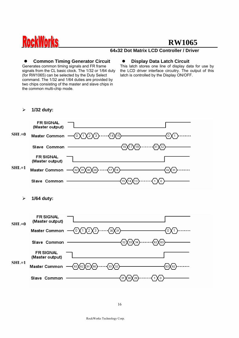
RW1065 64x32 Dot Matrix LCD Controller Driver
RockWorks Technology Corp
17
Display Timing Generator Circuit
The display timing generator circuit generates the timing signal to the line address circuit and the display data latch circuit using the display clock The display data is latched into the display data latch circuit synchronized with the display clock and is output to the data driver output terminal Reading to the display data liquid crystal driver circuits is completely independent of accesses to the display data RAM by the MPU Consequently even if the display data
RAM is accessed asynchronously during liquid crystal display there is absolutely no adverse effect (such asflickering) on the display Moreover the display timing generator circuit generates the common timing and the liquid crystal alternating current signal (FR) from the display clock It generates a drive wave form using a 2 frame alternating current drive method as is shown in Figure 5 for the liquid crystal drive circuit
Two-frame alternating current drive waveform
Figure 5
When multiple RW1065 Series chips are used the slave chip must be supplied the display timing signals(FR CL) from the master chip
Table 5 shows the status of the FR and CL signals
Table 5 Operating Mode FR CL
Master (MS = ldquoHrdquo) The internal oscillator circuit is enabled (CLS = ldquoHrdquo) The internal oscillator circuit is disabled (CLS = ldquoLrdquo)
Output Output
Output Input
Slave (MS = ldquoLrdquo) The internal oscillator circuit is enabled (CLS = ldquoHrdquo) The internal oscillator circuit is disabled (CLS = ldquoLrdquo)
Input Input
Input Input
RW1065 64x32 Dot Matrix LCD Controller Driver
RockWorks Technology Corp
18
The Liquid Crystal Driver Circuits
These are a 64-channel (RW1065) that generate four voltage levels for driving the liquid crystal The combination of the display data the COM scan signal and the FR signal
produces the liquid crystal drive voltage output Figure 6 shows examples of the SEG and COM output waveform
Figure 6
RW1065 64x32 Dot Matrix LCD Controller Driver
RockWorks Technology Corp
19
The Power Supply Circuit
The power supply circuits are low-power consumption power supply circuits that generate the voltage levels required for the liquid crystal drivers They comprise Booster circuits and voltage follower circuits They are only enabled in master operation The power supply circuits can turn on automatically after power on
Consequently it is possible to make an external power supply and the internal power supply function somewhat in parallel
The Liquid Crystal Voltage Generator Circuit The V0 voltage is produced by a resistive voltage divider outside the IC through VRAB pin and can be produced at the V1 V2 V3 and V4 voltage levels required for liquid crystal driving Moreover when the voltage follower changes the impedance it provides V1 V2 V3 and V4 to the liquid crystal drive circuit 15 bias or 16 bias or 18 bias or 19 bias for RW1065 can be selected by BS0 and BS1 pins V0-Vss maximum voltage is 15V Vout-Vss maximum voltage is 17V If VDD lt 35V it can use the Booster circuit 2x3x4xThe booster voltage can follow the spec condition (Vout-Vss ≦ 17V max voltage) if VDD gt35V only use the 2X3X booster circuit that can ensure the V0-Vss voltage ≦ 15V If use the VDD voltage 5V and 4X booster itrsquos over the spec operation condition To turn on built-in power (boosterfollower) must waiting 200mS to display on for boosterfollower stable Therefore power off must follower ldquopower off sequencerdquo too
Power on Display off
Power off
Power off sequence
Wait time gt200mS
Display on
Power on sequence
RW1065 64x32 Dot Matrix LCD Controller Driver
RockWorks Technology Corp
20
The Reset Circuit
When the RTP input comes to the ldquoLrdquo level these LSIs return to the default state Their default states are as follows 1 Display OFF 2 Display all point on is select to normal 3 Display normalreverse is select to normal 4 164 duty is selected 5 Read modify write OFF 6 Column address set to Address 0 7 Page address set to Page 0 8 Start line set to first line 9 Frame frequency set to default 10 Power save mode released 11 Ext set to ldquo0rdquo When the power is turned on the IC internal state becomes unstable and it is necessary to initialize it using the RSTP terminal After the initialization each input terminal should be controlled normally While RSTP is ldquoLrdquo the oscillator works but the display timing generator stops and the CL FR terminals are fixed to ldquoHrdquo The terminals D0 to D7 are not affected
RW1065 64x32 Dot Matrix LCD Controller Driver
RockWorks Technology Corp
21
TABLE OF RW1065 INSTRUCTIONS
Instruction code Instruction RS RW DB7 DB6 DB5 DB4 DB3 DB2 DB1 DB0 Description
EXT=0 or 1
MODE SET 0 0 0 0 0 0 1 1 0 EXT Set EXT mode
Instruction code Instruction RS RW DB7 DB6 DB5 DB4 DB3 DB2 DB1 DB0 Description
EXT=0 Display ONOFF 0 0 0 0 1 1 1 1 1 D D=0Display OFF
D=1Display ONSet page address 0 0 1 0 1 1 1 P2 P1 P0 Set page address
Set column address 0 0 0 1 Y5 Y4 Y3 Y2 Y1 Y0 Set column
address MSB
Read Status 0 1 BUSY 0 ON OFF RESET 0 0 0 0 Read register
status Write display
data 1 0 Write data Write data into DDRAM
Read display data 1 1 Read data Read data from
DDRAM Set initial
display line register
0 0 1 1 S5 S4 S3 S2 S1 S0 Specify the initial
display line to realize vertical scrolling
Instruction code Instruction RS RW DB7 DB6 DB5 DB4 DB3 DB2 DB1 DB0 Description
EXT=1
NOP 0 0 0 0 0 0 0 0 0 0 no operation
Set modiy-read 0 0 0 0 0 0 1 0 0 0 Set modiy-read
mode
END 0 0 0 0 0 0 1 1 1 0 release modiy-read mode
Set power save mode 0 0 0 0 0 0 0 0 1 PSAVE P=0 normal mode
P=1 sleep mode
0 0 0 0 0 1 0 1 Display
COMMAND (double
command)
0 0 FRSEL
0 0 0 0 REV ALLON DUTY
DUTY=1 64 duty DUTY=0 32 duty ALLON=1display all on ALLON=0display
normal REV=1display reverse REV=0display normal FRSEL=1FR frequency double default FRSEL=0FR frequency default
RW1065 64x32 Dot Matrix LCD Controller Driver
RockWorks Technology Corp
22
Command Description
See the Table of RW1065 instructions The RW1065 series identifies a data bus using a combination of RS E and RW signals As the MPU translates a command in the internal timing only (independent from the external clock) its speed is very high The busy check is usually not required
Display ONOFF
EXT RS RW D7 D6 D5 D4 D3 D2 D1 D0
0 0 0 0 0 1 1 1 1 1 D
This command turns the display on and off D=1 Display ON D=0 Display OFF(default)
Set page Address This command specifies the page address that corresponds to the low address of the display data RAM when it is accessed by the MPU Any bit of the display data RAM can be accessed when its page address and column address are specified The display status is not changed even when the page address is changed
EXT RS RW D7 D6 D5 D4 D3 D2 D1 D0
0 0 0 1 0 1 1 1 A2 A1 A0
This command loads the page address register
A2 A1 A0 Page
0 0 0 0 (default)
0 0 1 1 0 1 0 2 0 1 1 3 1 0 0 4 1 0 1 5 1 1 0 6 1 1 1 7
Page mapping see Figure 4
RW1065 64x32 Dot Matrix LCD Controller Driver
RockWorks Technology Corp
23
Set Column Address This command specifies a column address of the display data RAM When the display data RAM is accessed by the MPU continuously the column address is incremented by I each time it is accessed from the set address Therefore the MPU can access to data continuously The column address stops to be incremented at address 63 and the page address is not changed continuously
EXT RS RW D7 D6 D5 D4 D3 D2 D1 D0
0 0 0 0 1 A5 A4 A3 A2 A1 A0
A5 A4 A3 A2 A1 A0 Column Address0 0 0 0 0 0 0(default) 0 0 0 0 0 1 1
1 1 1 1 1 1 63
Read Status
EXT RS RW D7 D6 D5 D4 D3 D2 D1 D0
0 0 1 BUSY 0 ON OFF RESET 0 0 0 0
The BUSY Flag bit indicates that RW 1065 is operating or no operating
BUSY=1 Operation BUSY=0 Ready
The ONOFF bit indicates the current status of the display It is the inverse of the polarity of the display ONOFF command ONOFF=1 Display OFF ONOFF=0 Display ON The RESET bit indicates whether the driver is executing a hardware or software reset or if it is in normal operating mode RESET=1 Currently executing reset command RESET=0 Normal operation
RW1065 64x32 Dot Matrix LCD Controller Driver
RockWorks Technology Corp
24
Write Display Data
EXT RS RW D7 D6 D5 D4 D3 D2 D1 D0
0 1 0 Write data
Writes 8-bits of data into the display data RAM at a location specified by the contents of the column address and page address registers and then increments the column address register by one
Read Display Data
EXT RS RW D7 D6 D5 D4 D3 D2 D1 D0
0 1 1 Read data
Reads 8-bits of data from the data IO latch updates the contents of the IO latch with display data from the display data RAM location specified by the contents of the column address and page address registers and then increments the column address register After loading a new address into the column address register one dummy read is required before valid data is obtained
Set initial display line register
EXT RS RW D7 D6 D5 D4 D3 D2 D1 D0
0 0 0 1 1 S5 S4 S3 S2 S1 S0
Loads the RAM line address of the initial display line COM 0 into the initial display line register The RAM display data becomes the top line of the LCD screen It is followed by the higher number lines in ascending order corresponding to the duty cycle The screen can be scrolled using this command by incrementing the line address(default value=rdquo00Hrdquo)
RW1065 64x32 Dot Matrix LCD Controller Driver
RockWorks Technology Corp
25
Read-Modify-Write
EXT RS RW D7 D6 D5 D4 D3 D2 D1 D0
1 0 0 0 0 0 0 1 0 0 0
This command defeats column address register auto-increment after data reads The current contents of the column Address register are saved The mode remains active until an End command is received When the End command is entered the column address is returned to the one used during input of Read-Modify-Write Command This function can reduce the load of MPU when data change is repeated as a specific display area Any command other than Data Read or Write can be used in the Read-Modify-Write mode However the Column Address Set command cannot be used
End
EXT RS RW D7 D6 D5 D4 D3 D2 D1 D0
1 0 0 0 0 0 0 1 1 1 0
This command cancels read-modify-write mode and restores the contents of the column address register to their value prior to the receipt of the Read-Modify-Write command
N N+1 N+2 N+3 N+m N
Read -modify-write mode set End
Returm
Column address
Set page address
Set column address
Read-modify-write
Dummy read
Read data
Write data
End
CompletedNo
Yes
RW1065 64x32 Dot Matrix LCD Controller Driver
RockWorks Technology Corp
26
Set power save mode
EXT RS RW D7 D6 D5 D4 D3 D2 D1 D0
1 0 0 0 0 0 0 0 0 1 PSAVE
When power save mode is entered thus greatly reducing power consumption In the power save mode the display data is saved as is the operating mode that was in effect before the power saver mode was initiated and the MPU is still able to access the display data RAM PSAVE=1 Sleep mode PSAVE=0 Normal mode Sleep mode This stops all operations in the LCD display system and as long as there are no accesses from the MPU the consumption current is reduced to a value near the static current The internal modes during sleep mode are as follows 1 The oscillator circuit and the LCD power supply circuit are halted 2 All liquid crystal drive circuits are halted and the segment and common drive outputs output a Vss level
Display command double command
EXT RS RW D7 D6 D5 D4 D3 D2 D1 D0
1 0 0 0 0 0 0 0 1 0 1
1 0 0 FRSEL 0 0 0 0 REV ALLON DUTY
Display NormalReverse set REV=1 Reverse REV=0 Normal(default) Display All Point ONOFF ALLON=1 All display points ON ALLON=0 Normal(default) Select Duty Duty=1 164 duty cycle(default) Duty=0 132 duty cycle FRAME FREQUENCY Select FRSEL=1 Double FRSEL=0 (default)
RW1065 64x32 Dot Matrix LCD Controller Driver
RockWorks Technology Corp
27
Hardware Pin Set
Select ADC by ADC Pin The pin selects the relationship between display data RAM column addresses and segment drivers ADC=1 SEG0larrcolumn address 3FHhellipinverted ADC=0 SEG0larrcolumn address 00Hhellipnormal(default) This command is provided to reduce restrictions on the placement of driver ICs and routing of traces during printed circuit Board design See Figure 4 for a table of segments and column addresses for the two values of D
Select SHL by SHL Pin The pin selects the com output scan direction SHL=1 Reverse directioncom63rarrcom0 SHL=0 Normal com0rarrcom63 Both master and slave should set identical SHL value
Select LCD Bias by BS0 BS1 Pin
BS1 BS0 Bias 0 0 15 bias 0 1 16 bias 1 0 18 bias 1 1 19 bias
RW1065 64x32 Dot Matrix LCD Controller Driver
RockWorks Technology Corp
28
When an External Resistance is Used The liquid crystal power supply voltage V0 is set by adding resistors Rarsquo and Rbrsquo between VDD and VR and between VR and V0 respectively
RW1065
RW1065 64x32 Dot Matrix LCD Controller Driver
RockWorks Technology Corp
29
The set voltage circuits
Using the step-up voltage circuits equipped within the RW1065 chips it is possible to produce a 2X 3X 4X step-up voltage levels 2X step-up
To produce voltage level in the positive direction at the Vout terminal that is 2 times the voltage difference between VSS and VDD2 Please configure set voltage circuits like this Place a 1uF~22uF capacitor between CAP1N and CAP1P Place a 1uF~22uF capacitor between VSS and VOUT Short CAP2P CAP3P and VOUT Leave CAP2N open 3X step-up
To produce voltage level in the positive direction at the Vout terminal that is 3 times the voltage difference between VSS and VDD2 Please configure set voltage circuits like this Place a 1uF~22uF capacitor between CAP1N and CAP1P Place a 1uF~22uF capacitor between VSS and VOUT Place a 1uF~22uF capacitor and 100 ohms resistor between CAP2N and CAP2P Short CAP3P and Vout 4X step-up
To produce voltage level in the positive direction at the Vout terminal that is 4 times the voltage difference between VSS and VDD2 Please configure set voltage circuits like this Place a 1uF~22uF capacitor between CAP1N and CAP1P Place a 1uF~22uF capacitor between VSS and VOUT Place a 1uF~22uF capacitor and 100 ohms resistor between CAP2N and CAP2P Place a 1uF~22uF capacitor and 100 ohms resistor between CAP1N and CAP3P
RW1065 64x32 Dot Matrix LCD Controller Driver
RockWorks Technology Corp
30
ABSOLUTE MAXIMUM RATINGS Characteristics Symbol Value Unit
Power supply voltage VDD -03 to +70 V
LCD driver voltage Vout 0 to +17 V
Input voltage VIN -03 to VDD+03 V
Operating temperature TA -40 to +85
Storage temperature TSTO -55 to +125
DC CHARACTERISTICS
Rating Item Symbol Condition Min Typ Max Unit ApplicablePin
Operating Voltage VDD - 27 30 55 V VDD1
Step up output voltage Vout (Relative to VDD) 0 - 17 V Vout
Voltage follower circuit operating Voltage V0 (Relative to VDD) 0 - 15 V V0
V0 accuracy V0 - 0 - 15 V0
High-level Input Voltage Low-level Input Voltage
VIHC VILC - 07 VDD
Vss - VDD 09 V 2
High-level Output Voltage Low-level Output Voltage
VOHC VOLC
IOH = ndash05 mA IOL = 05 mA
08VDD Vss - VDD
02 VDD V 3
Input leakage current ILI VIN = VDD or VSS -1 - 2 uA 4
Output leakage current ILO - -1 1 uA 5
Liquid Crystal Driver ON Resistance RON
Ta= 25degC(Relative To VDD)
V0 =15 V - 16 20 KΩ SEGn COMn 6
Internal Oscillator fOSC 2286 254 2794 Oscillator
Frequency External Input RECOMMAND fCL
Ta = 25degC 132Duty 2286 254 2794
kHz CL
Internal Oscillator fOSC 45 5 55 Oscillator
Frequency External Input RECOMMAND fCL
Ta = 25degC 164Duty 45 5 55
kHz CL
bullDynamic Consumption Current During Display with the Internal Power Supply OFF Current consumed by total ICs when an external power supply is used
Unless otherwise specified Vss=0V VDD=30V
RW1065 64x32 Dot Matrix LCD Controller Driver
RockWorks Technology Corp
31
Display Pattern OFF
Ta = 25degC Vout=17V Rating Item Symbol Condition Min Typ Max Unit Notes
VDD=30 V V0-Vss=8V - 10 15 RW1065 IDD VDD=50 V V0-Vss=8V - 35 45
microA 7
Display Pattern Checker
Ta = 25degC Vout=17V Rating Item Symbol Condition Min Typ Max Unit Notes
VDD=30 V V0-Vss=8V - 15 20 RW1065 IDD VDD=50 V V0-Vss=8V - 40 50
microA 7
Display Pattern OFF
Ta = 25degC Vout=17V Rating Item Symbol Condition Min Typ Max Unit Notes
VDD=30 V V0-Vss=8V - 15 20 RW1065 IDD VDD=50 V V0-Vss=8V - 40 50
microA 7
Display pattern Checker
Ta = 25degC Vout=17V Rating Item Symbol Condition Min Typ Max Unit Notes
VDD=30 V V0-Vss=8V - 65 80 RW1065 IDD VDD=50 V V0-Vss=8V - 130 150
microA 7
bull Consumption Current at Time of Power Saver Mode VSS = 0 V VDD = 30 V plusmn 10
Rating Item Symbol Condition Min Typ Max Unit Notes
Sleep mode IDD - - 5 10 microA -
References for items market with 1 While a broad range of operating voltages is guaranteed performance cannot be guaranteed if there are sudden fluctuations to the
voltage while the MPU is being accessed 2 The RS D0 to D5 D6 D7 E RW CS1BP CS2P CLS CL FR MS and RST
― terminals
3 The D0 to D7 FR and CL terminals 4 The RS E RW CS1BP CS2P CLS MS and RST
― terminals
5 Applies when the D0 to D5 D6 D7 CL and FR terminals are in a high impedance state 6 These are the resistance values for when a 01 V voltage is applied between the output terminals SEGn or COMn and
the various power supply terminals (V1 V2 V3 and V4) These are specified for the operating voltage (3) range RON = 01 V ∆I (Where ∆I is the current that flows when 01 V is applied while the power supply is ON)
7 It indicates the current consumed on ICs alone when the internal oscillator circuit and display are turned on Does not include the current due to the LCD panel capacity and wiring capacity Applicable only when there is no access from the MPU
RW1065 64x32 Dot Matrix LCD Controller Driver
RockWorks Technology Corp
32
TIMING CHARACTERISTICS
68 Interface
(Ta=-40 to 85 degC) VDD=27 to 45V
Rating VDD=45 to 55V
Rating Item Signal Symbol ConditionMin Max Min Max
Units
Address hold time RS tAH6 0 mdash 0 mdash Address setup time RS tAW6
mdash 0 mdash 0 mdash
ns
System cycle time RS tCYC6 mdash 900 mdash 800 mdash ns Data setup time D0 to D7 tDS6 100 mdash 100 mdash Data hold time D0 to D7 tDH6
mdash 0 mdash 0 mdash
ns
Access time D0 to D7 tACC6 mdash 350 mdash 250
Output disable time D0 to D7 tOH6 CL = 100 pF
mdash 300 mdash 200 ns
Read tEWHR 360 mdash 300 mdash Enable H pulse time
WriteE
tEWHW mdash
360 mdash 300 mdash ns
Read tEWLR 450 mdash 400 mdash Enable L pulse time
WriteE
tEWLW mdash
450 mdash 400 mdash ns
1 All timing is specified using 20 and 80 of VDD as the reference 2 tEWLW and tEWLR are specified as the overlap between CS1BP being ldquoLrdquo (CS2P = ldquoHrdquo) and E
RW1065 64x32 Dot Matrix LCD Controller Driver
RockWorks Technology Corp
33
Reset Timing
Rating Item Signal Symbol Condition
Min Typ Max Units
Reset time mdash tR mdash mdash - 2 micros
Reset ldquoLrdquo pulse width RST tRW mdash 2 - mdash micros
1 When double chip was be used then the duty set command must be set between the tR
RW1065 64x32 Dot Matrix LCD Controller Driver
RockWorks Technology Corp
34
IO PAD CONFIGURATION
RW1065 64x32 Dot Matrix LCD Controller Driver
RockWorks Technology Corp
35
THE MPU INTERFACE (REFERENCE EXAMPLES) The RW1065 Series can be connected to 6800 Series MPUs The display area can be enlarged by using multiple RW1065 Series chips When this is done the chip select signal can be used to select the individual ICs to access
6800 Series MPUs
RW
106
5
RW1065 64x32 Dot Matrix LCD Controller Driver
RockWorks Technology Corp
36
When using external multi-level power supply for LCD driving (REFERENCE EXAMPLE)
Using a resistor divider can provide RW1065 external multi-level power supply for LCD driving
The circuit below shows a resistor divider network which can bias V0 V1 V2 V3 and V4 externally
RW1065 64x32 Dot Matrix LCD Controller Driver
RockWorks Technology Corp
37
bullWhen V0 V1 V2 V3 and V4 are biased by external power supply analog section of RW1065 should be turn off by software during LCD initialization The example in below shows the sequence to turn off analog section when external bias is used Begin of LCD initialization 1 Reset RW1065 2 SET EXT=1 (mode instruction)
RS RW DB7 DB6 DB5 DB4 DB3 DB2 DB1 DB00 0 0 0 0 0 1 1 0 1
3 SET Display Command (double command)
RS RW DB7 DB6 DB5 DB4 DB3 DB2 DB1 DB00 0 0 0 0 0 0 1 0 1 0 0 0 0 1 1 0 0 0 1
4 SET EXT=1 (mode instruction)
RS RW DB7 DB6 DB5 DB4 DB3 DB2 DB1 DB00 0 0 0 0 0 1 1 0 0
End of LCD initialization
bullBecause pins can not set LCD bias when external power supplies are used for LCD driving the bias can be set by an appropriate configuration for a resistor voltage divider networks The example is shown below
VSS
R
R
NR
R
R
RV1
RV2
RV3
RV4
V0
Bias Network Circuit Concept 15 Bias N=1 total = 5R 16 Bias N=2 total =6R 18 Bias N=4 total =8R 19 Bias N=5 total = 9R
RW1065 64x32 Dot Matrix LCD Controller Driver
RockWorks Technology Corp
38
Single chip solution for RW1065 application (REFERENCE EXAMPLE)
For a 64x32 application the duty cycle of LCD panel is 164 and the display duty of RW1065 should be set to 164 The display duty cycle can be selected by the DUTY bit in display command The diagram for 64x32 application is shown below
64 SEGx32COM LCD Panel
164 duty cycle
RW1065 DUTY=1
COM1~33
SEG1~65
RW1065 64x32 Dot Matrix LCD Controller Driver
RockWorks Technology Corp
39
Using an adjustable resistor on the main board to adjust the contrast of liquid crystal display (REFERENCE EXAMPLE)
The schematic shows an adjustable resistor on main board that can adjust voltage level of V0
RW1065 64x32 Dot Matrix LCD Controller Driver
RockWorks Technology Corp
40
Package information (Please pay close attention to the information in this section Do not hesitate to consult with our sale representative if you have any question or concern)
In order to make better bonding yield for RW1065 please follow the tips and recommendations in this section In this section few tips about COB footprint style PCB layout and wire bonding will be discussed
The drawing in below shows the PCB footprint style which we recommend for RW1065 Pads array in
curve shape is easier for Al wire bonding Besides that a real size COB footprint for RW1065 is also shown in below RW1065 COB footprint is also available in powerpcb or protel format for design reference purpose
The ratio is 11
RW1065 64x32 Dot Matrix LCD Controller Driver
RockWorks Technology Corp
41
During COB footprint design there have some tips about footprint that the PCB designer should know The angle between bonding wire and vertical line should less than 45 Otherwise the wire shorts would become very easy to happen at fours corners of the chip
The angle between bonding wire and vertical line could be reduced by expanding the distance between pads array and the chip In addition reducing length in horizon direction of pads array could minimize the angle between bonding wire and vertical line The picture in below will help to illustrate this concept From the experiences COB footprint style affects the bonding yield
Bad Wires are too close to each other
The angle between bonding wire and vertical line is greater than 45
The angle between bonding wire and vertical line is less than 45
Wires are not too close to each other
Reducing length in horizon direction of pads array could minimize the angle between bonding wire and vertical line
The angle between bonding wire and vertical line could be reduced by expanding the distance between pads array and the chip
RW1065 64x32 Dot Matrix LCD Controller Driver
RockWorks Technology Corp
42
If the gap between pads of COB footprint is filled with solder mask coating it is difficult to bond Al wire to
the pads The top solder masks layer that overlap COB footprint area should be removed
Please use 1 mils diameter Al wire for RW1065 wire bonding
1 2 3 4 5 6
A
B
C
D
654321
D
C
B
A
Title
Number RevisionSize
C
Date 29-Aug-2007 Sheet of File D公司資料99seMyDesignddb Drawn By
RW1065
COM131
COM142
COM153
COM164
COM175
COM186
COM197
COM208
COM219
COM2210
COM2311
COM2412
COM2513
COM2614
COM2715
COM2816
COM2917
COM3018
COM3119
SEG
6320
SEG
6221
SEG
6122
SEG
6023
SEG
5924
SEG
5825
SEG
5726
SEG
5627
SEG
5528
SEG
5429
SEG
5330
SEG
5231
SEG
5132
SEG
5033
SEG
4934
SEG
4835
SEG
4736
SEG
4637
SEG
4538
SEG
4439
SEG
4340
SEG
4241
SEG
4142
SEG
4043
SEG
3944
SEG
3845
SEG
3746
SEG
3647
SEG
3548
SEG
3449
SEG
3350
SEG
3251
SEG
3152
SEG
3053
SEG
2954
SEG
2855
SEG
2756
SEG
2657
SEG
2558
SEG
2459
SEG
2360
SEG
2261
SEG
2162
SEG
2063
SEG
1964
SEG
1865
SEG
1766
SEG
1667
SEG
1568
SEG
1469
SEG13 70SEG12 71SEG11 72SEG10 73SEG9 74SEG8 75SEG7 76SEG6 77SEG5 78SEG4 79SEG3 80SEG2 81SEG1 82SEG0 83ADCP 84CLL 85
VSS
86D
087
D1
88D
289
D3
90D
491
D5
92D
693
D7
94C
S1B
P95
CS2
P96
ERD
P97
AO
P(R
S)98
RW
RP
99V
DD
100
RST
P10
1C
LSP
102
FRR
103
MSP
104
BS1
P10
5B
S0P
106
SHLP
107
VD
D2
108
CA
P2N
109
CA
P2P
110
CA
P1P
111
CA
P1N
112
CA
P3P
113
VO
UT
114
V0
115
VR
AB
116
V3
117
V2
118
V4
119
V1
120
CO
M0
121
CO
M1
122
CO
M2
123
CO
M3
124
CO
M4
125
CO
M5
126
CO
M6
127
CO
M7
128
CO
M8
129
CO
M9
130
CO
M10
131
CO
M11
132
CO
M12
133
4897x1902 um
IC1
RW1065
C9CAPR4
100R0603
R30R0603
C8
CAP
C7
CAP
R2
100R0603
R1
0R0603C6 22uf
R50R
R6300R
R7RES1
R8NC R9
100R0603
VDD
R10
NC
R11
100R0603
R12
100R0603
R13
NC
R14
100R0603
R15
NC
VDD
D0
D1
D2
D3
D4
D5
D6
D7
DB[07]
VDDC5
01uf0603
VD
D
CS2
P
123456789
1011121314151617181920
J1
CON20
C1201uf0603
R3951K0603
VDD
CAP Value1UF~22UF
2XPut C6C8 Short R1R3Open R2R4C7C93XPut C6C8C9 R4Short R1Open R2R3C74XOpen R1R3
BS0 BS1 Bias0 0
0 1
1 0
11
15 bias
16 bias
18 bias
19 bias
ADC=0 SEG0lt~column address 00Hnormal(default) ADC=1 SEG0lt~column address 3FHinverted
SHL=0 Normal COM0~gtCOM63(default)SHL=1 Reverse direction COM63~gtCOM0
R16100R0603
LCD PANEL 64X32RockWorks
RW1065 64X32
COM0-31 SEG0-63SHL=0 ADC=0
SHL=1COM31-0
ADC=1SEG63-0
if use single chip for 32 command displaythe display command must select 164 dutyDisplay panel must select 164 duty type
VO
UT
C3P
C1N
C1P
C2P
C2N
VDD2
ADC
SHL
BS0
BS1
CLLADC
V1
V2
V3
V4
VR
AB
V0
VO
UT
C3P
C1N
C1P
C2P
C2N
VD
D2
SHL
BS0
BS1
FRR
RST
P
RW
RS
E CS1
B
CS1
V0RSRWED0D1D2D3D4D5D6D7
RSTPAK
C4
22uf
RBRES1
RA1RES1
C2
22uf
C1
22uf
C3
22uf
C0
22uf
R20
100k0603
R21
100k0603
R17
200K0603
V1
V2
V3
V4 VRAB
V0
V0
OPTION
B
R18
300R0603
RA2RES1
VADJ
R19100R
R23 RES1R22 0R
R24
RES1
R25
0R
VDD
CS1BP
CS2P
CS1
CS1
R26
22R0603
R27
22R0603
C1047uf
C11
01uf
VSS_INVDD_IN
D1DIODE
FGND
鐵框地
VSS
VDD
R28 10RR29 10RR30 10RR31 10RR32 10RR33 10RR34 10RR35 10RR36 10RR37 10RR38 10R
VADJ
1 2 3 4 5 6
A
B
C
D
654321
D
C
B
A
Title
Number RevisionSize
C
Date 29-Aug-2007 Sheet of File D公司資料99seMyDesignddb Drawn By
RW1065
COM131
COM142
COM153
COM164
COM175
COM186
COM197
COM208
COM219
COM2210
COM2311
COM2412
COM2513
COM2614
COM2715
COM2816
COM2917
COM3018
COM3119
SEG
6320
SEG
6221
SEG
6122
SEG
6023
SEG
5924
SEG
5825
SEG
5726
SEG
5627
SEG
5528
SEG
5429
SEG
5330
SEG
5231
SEG
5132
SEG
5033
SEG
4934
SEG
4835
SEG
4736
SEG
4637
SEG
4538
SEG
4439
SEG
4340
SEG
4241
SEG
4142
SEG
4043
SEG
3944
SEG
3845
SEG
3746
SEG
3647
SEG
3548
SEG
3449
SEG
3350
SEG
3251
SEG
3152
SEG
3053
SEG
2954
SEG
2855
SEG
2756
SEG
2657
SEG
2558
SEG
2459
SEG
2360
SEG
2261
SEG
2162
SEG
2063
SEG
1964
SEG
1865
SEG
1766
SEG
1667
SEG
1568
SEG
1469
SEG13 70SEG12 71SEG11 72SEG10 73SEG9 74SEG8 75SEG7 76SEG6 77SEG5 78SEG4 79SEG3 80SEG2 81SEG1 82SEG0 83ADCP 84CLL 85
VSS
86D
087
D1
88D
289
D3
90D
491
D5
92D
693
D7
94C
S1B
P95
CS2
P96
ERD
P97
AO
P(R
S)98
RW
RP
99V
DD
100
RST
P10
1C
LSP
102
FRR
103
MSP
104
BS1
P10
5B
S0P
106
SHLP
107
VD
D2
108
CA
P2N
109
CA
P2P
110
CA
P1P
111
CA
P1N
112
CA
P3P
113
VO
UT
114
V0
115
VR
AB
116
V3
117
V2
118
V4
119
V1
120
CO
M0
121
CO
M1
122
CO
M2
123
CO
M3
124
CO
M4
125
CO
M5
126
CO
M6
127
CO
M7
128
CO
M8
129
CO
M9
130
CO
M10
131
CO
M11
132
CO
M12
133
4897x1902 um
IC1
RW1065 Master
RW1065
COM131
COM142
COM153
COM164
COM175
COM186
COM197
COM208
COM219
COM2210
COM2311
COM2412
COM2513
COM2614
COM2715
COM2816
COM2917
COM3018
COM3119
SEG
6320
SEG
6221
SEG
6122
SEG
6023
SEG
5924
SEG
5825
SEG
5726
SEG
5627
SEG
5528
SEG
5429
SEG
5330
SEG
5231
SEG
5132
SEG
5033
SEG
4934
SEG
4835
SEG
4736
SEG
4637
SEG
4538
SEG
4439
SEG
4340
SEG
4241
SEG
4142
SEG
4043
SEG
3944
SEG
3845
SEG
3746
SEG
3647
SEG
3548
SEG
3449
SEG
3350
SEG
3251
SEG
3152
SEG
3053
SEG
2954
SEG
2855
SEG
2756
SEG
2657
SEG
2558
SEG
2459
SEG
2360
SEG
2261
SEG
2162
SEG
2063
SEG
1964
SEG
1865
SEG
1766
SEG
1667
SEG
1568
SEG
1469
SEG13 70SEG12 71SEG11 72SEG10 73SEG9 74SEG8 75SEG7 76SEG6 77SEG5 78SEG4 79SEG3 80SEG2 81SEG1 82SEG0 83ADCP 84CLL 85
VSS
86D
087
D1
88D
289
D3
90D
491
D5
92D
693
D7
94C
S1B
P95
CS2
P96
ERD
P97
AO
P(R
S)98
RW
RP
99V
DD
100
RST
P10
1C
LSP
102
FRR
103
MSP
104
BS1
P10
5B
S0P
106
SHLP
107
VD
D2
108
CA
P2N
109
CA
P2P
110
CA
P1P
111
CA
P1N
112
CA
P3P
113
VO
UT
114
V0
115
VR
AB
116
V3
117
V2
118
V4
119
V1
120
CO
M0
121
CO
M1
122
CO
M2
123
CO
M3
124
CO
M4
125
CO
M5
126
CO
M6
127
CO
M7
128
CO
M8
129
CO
M9
130
CO
M10
131
CO
M11
132
CO
M12
133
4897x1902 um
IC2
RW1065 Slave
C4
22uf
RBRES1
RA1RES1
C2
22uf
C1
22uf
C3
22uf
C0
22ufC9CAPR4
100R0603
R30R0603
C8
CAP
C7
CAP
R2
100R0603
R1
0R0603C6 22uf
R50R0603
R6300R0603
R7RES1
R8NC R9
100R0603
VDD
R10
NC
R11
100R0603
R12
NC
R13
100R0603
R14
100R0603
R15
NC
R16
100R0603
R17
NC
VDD
D0
D1
D2
D3
D4
D5
D6
D7
D0
D1
D2
D3
D4
D5
D6
D7
DB[07] DB[07]
VDDC10
01uf0603
VD
D
IC1_
CS2
P
VDD
IC2_
CS2
P
VD
D
C11
01uf0603
VSS
VSS
LCD PANEL 128X64
Master COM0-31 Slave COM32-63
Master SEG0-63 Slave SEG64-127
123456789
1011121314151617181920
J1
CON20
Master Slave
CAP Value1UF~22UF
2XPut C6C8 Short R1R3Open R2R4C7C93XPut C6C8C9 R4Short R1Open R2R3C74XOpen R1R3
RockWorksRW1065 128x64
BS0 BS1 Bias0 0
0 1
1 0
11
15 bias
16 bias
18 bias
19 bias
ADC=0 SEG0lt~column address 00Hnormal(default) ADC=1 SEG0lt~column address 3FHinverted
SHL=0 Normal COM0~gtCOM63(default)SHL=1 Reverse direction COM63~gtCOM0Both Master and Slave should set identical SHL value
SHL=0 SHL=0
ADC=0 ADC=0
Slave COM31-0
Slave SEG127-64
SHL=1
ADC=1
SHL=1Master COM63-32
ADC=1Master SEG63-0
R18100R0603
R22
100k0603
R23
100k0603
C501uF0603
R4551K0603
VDD
R19
200K0603
ADC1
ADC2
SHL
BS0
BS1
VDD2
V1
V2
V3
V4 VRAB
V0
V0V
OU
T
C3P
C1N
C1P
C2P
C2N
V1
V2
V3
V4
VR
AB
V0
VO
UT
C3P
C1N
C1P
C2P
C2N
VD
D2
SHL
BS0
BS1
FRR
RST
P
RW
RS
E IC1_
CS1
BP
V1
V2
V3
V4
VR
AB
V0
VO
UT
VD
D2
SHL
BS0
BS1
FRR
RST
P
RW
RS
E IC2_
CS1
BP
CLLADC1
CLLADC2
RSTP
CS1CS2
V0RSRWED0D1D2D3D4D5D6D7
AK
OPTION
R20
300R0603
RA2RES1
VADJ
R21
100R
B
R25 RESR24 0R
R26 RES R27 0RVDD
IC1_CS1BP
IC1_CS2P
CS1
CS1
R28 0R R29 RES
R30 RES R31 0R
IC2_CS1BP
IC2_CS2P
CS2
CS2
R32
22R0603
R33
22R0603
C1001uf
C11
47uf
D1DIODE
FGND
鐵框地
VSS
VDD
R34 10RR35 10RR36 10RR37 10RR38 10RR39 10RR40 10RR41 10RR42 10RR43 10RR44 10R
VSS_INVDD_IN
VADJ
VDD
1 2 3 4 5 6 7 8
A
B
C
D
87654321
D
C
B
A
Title
Number RevisionSize
D
Date 29-Aug-2007 Sheet of File D公司資料 99seMyDesignddb Drawn By
C422uf
RBRES1
RA1RES1
C3
22uf
C2
22uf
C1
22uf
C0
22ufC9CAPR4
100R0603
R30R0603
C8
CAP
C7
CAP
R2
100R0603
R1
0R0603C6 22uf
R220R0603
R23300R0603
R24RES1
R39
NCR40
100 ohm0603
VDD
R41
NC
R42
100 ohm0603
R43
NC
R44
100 ohm0603
R45
NC
R46
100 ohm0603
R47
100 ohm0603
R48
NC
R49
100 ohm0603
R50
NC
VDDCAP Value1UF~22UF
2XPut C6C8 Short R1R3Open R2R4C7C93XPut C6C8C9 R4Short R1Open R2R3C74XOpen R1R3
BS0 BS1 Bias0 0
0 1
1 0
11
15 bias
16 bias
18 bias
19 bias
ADC=0 SEG0lt~column address 00Hnormal(default)
ADC=1 SEG0lt~column address 3FHinverted
SHL=0 Normal COM0~gtCOM63(default)SHL=1 Reverse direction COM63~gtCOM0Both Master and Slave should set identical SHL value
R7
100k0603
R8
100k0603
V1
V2
V3
V4
V0
VRAB
V0
R5
200K
VDD2
VO
UT
C3P
C1N
C1P
C2P
C2N
ADC1
ADC2
ADC3
SHL
BS0
BS1
CS1CS2CS3
V0RSRWED0D1D2D3D4D5D6D7
RSTP
R3851K0603
C5
01uF
VDD
OPTION
R6
300R0603R9100R
RA2RES1
VADJ
RW1065
COM131
COM142
COM153
COM164
COM175
COM186
COM197
COM208
COM219
COM2210
COM2311
COM2412
COM2513
COM2614
COM2715
COM2816
COM2917
COM3018
COM3119
SEG
6320
SEG
6221
SEG
6122
SEG
6023
SEG
5924
SEG
5825
SEG
5726
SEG
5627
SEG
5528
SEG
5429
SEG
5330
SEG
5231
SEG
5132
SEG
5033
SEG
4934
SEG
4835
SEG
4736
SEG
4637
SEG
4538
SEG
4439
SEG
4340
SEG
4241
SEG
4142
SEG
4043
SEG
3944
SEG
3845
SEG
3746
SEG
3647
SEG
3548
SEG
3449
SEG
3350
SEG
3251
SEG
3152
SEG
3053
SEG
2954
SEG
2855
SEG
2756
SEG
2657
SEG
2558
SEG
2459
SEG
2360
SEG
2261
SEG
2162
SEG
2063
SEG
1964
SEG
1865
SEG
1766
SEG
1667
SEG
1568
SEG
1469
SEG13 70SEG12 71SEG11 72SEG10 73SEG9 74SEG8 75SEG7 76SEG6 77SEG5 78SEG4 79SEG3 80SEG2 81SEG1 82SEG0 83ADCP 84CLL 85
VSS
86D
087
D1
88D
289
D3
90D
491
D5
92D
693
D7
94C
S1B
P95
CS2
P96
ERD
P97
AO
P(R
S)98
RW
RP
99V
DD
100
RST
P10
1C
LSP
102
FRR
103
MSP
104
BS1
P10
5B
S0P
106
SHLP
107
VD
D2
108
CA
P2N
109
CA
P2P
110
CA
P1P
111
CA
P1N
112
CA
P3P
113
VO
UT
114
V0
115
VR
AB
116
V3
117
V2
118
V4
119
V1
120
CO
M0
121
CO
M1
122
CO
M2
123
CO
M3
124
CO
M4
125
CO
M5
126
CO
M6
127
CO
M7
128
CO
M8
129
CO
M9
130
CO
M10
131
CO
M11
132
CO
M12
133
4897x1902 um
IC1
RW1065 Master
RW1065
COM131
COM142
COM153
COM164
COM175
COM186
COM197
COM208
COM219
COM2210
COM2311
COM2412
COM2513
COM2614
COM2715
COM2816
COM2917
COM3018
COM3119
SEG
6320
SEG
6221
SEG
6122
SEG
6023
SEG
5924
SEG
5825
SEG
5726
SEG
5627
SEG
5528
SEG
5429
SEG
5330
SEG
5231
SEG
5132
SEG
5033
SEG
4934
SEG
4835
SEG
4736
SEG
4637
SEG
4538
SEG
4439
SEG
4340
SEG
4241
SEG
4142
SEG
4043
SEG
3944
SEG
3845
SEG
3746
SEG
3647
SEG
3548
SEG
3449
SEG
3350
SEG
3251
SEG
3152
SEG
3053
SEG
2954
SEG
2855
SEG
2756
SEG
2657
SEG
2558
SEG
2459
SEG
2360
SEG
2261
SEG
2162
SEG
2063
SEG
1964
SEG
1865
SEG
1766
SEG
1667
SEG
1568
SEG
1469
SEG13 70SEG12 71SEG11 72SEG10 73SEG9 74SEG8 75SEG7 76SEG6 77SEG5 78SEG4 79SEG3 80SEG2 81SEG1 82SEG0 83ADCP 84CLL 85
VSS
86D
087
D1
88D
289
D3
90D
491
D5
92D
693
D7
94C
S1B
P95
CS2
P96
ERD
P97
AO
P(R
S)98
RW
RP
99V
DD
100
RST
P10
1C
LSP
102
FRR
103
MSP
104
BS1
P10
5B
S0P
106
SHLP
107
VD
D2
108
CA
P2N
109
CA
P2P
110
CA
P1P
111
CA
P1N
112
CA
P3P
113
VO
UT
114
V0
115
VR
AB
116
V3
117
V2
118
V4
119
V1
120
CO
M0
121
CO
M1
122
CO
M2
123
CO
M3
124
CO
M4
125
CO
M5
126
CO
M6
127
CO
M7
128
CO
M8
129
CO
M9
130
CO
M10
131
CO
M11
132
CO
M12
133
4897x1902 um
IC2
RW1065 Slave
D0
D1
D2
D3
D4
D5
D6
D7
D0
D1
D2
D3
D4
D5
D6
D7
DB[07] DB[07]
VDDC8
01uf0603
VD
D
VDD
VD
D
C9
01uf0603
VSS
VSS
LCD PANEL 192X64
Master COM0-31 Slave COM32-63
Master SEG0-63 Slave SEG64-127
Master Slave
RockWorksRW1065 192x64
RW1065
COM131
COM142
COM153
COM164
COM175
COM186
COM197
COM208
COM219
COM2210
COM2311
COM2412
COM2513
COM2614
COM2715
COM2816
COM2917
COM3018
COM3119
SEG
6320
SEG
6221
SEG
6122
SEG
6023
SEG
5924
SEG
5825
SEG
5726
SEG
5627
SEG
5528
SEG
5429
SEG
5330
SEG
5231
SEG
5132
SEG
5033
SEG
4934
SEG
4835
SEG
4736
SEG
4637
SEG
4538
SEG
4439
SEG
4340
SEG
4241
SEG
4142
SEG
4043
SEG
3944
SEG
3845
SEG
3746
SEG
3647
SEG
3548
SEG
3449
SEG
3350
SEG
3251
SEG
3152
SEG
3053
SEG
2954
SEG
2855
SEG
2756
SEG
2657
SEG
2558
SEG
2459
SEG
2360
SEG
2261
SEG
2162
SEG
2063
SEG
1964
SEG
1865
SEG
1766
SEG
1667
SEG
1568
SEG
1469
SEG13 70SEG12 71SEG11 72SEG10 73SEG9 74SEG8 75SEG7 76SEG6 77SEG5 78SEG4 79SEG3 80SEG2 81SEG1 82SEG0 83ADCP 84CLL 85
VSS
86D
087
D1
88D
289
D3
90D
491
D5
92D
693
D7
94C
S1B
P95
CS2
P96
ERD
P97
AO
P(R
S)98
RW
RP
99V
DD
100
RST
P10
1C
LSP
102
FRR
103
MSP
104
BS1
P10
5B
S0P
106
SHLP
107
VD
D2
108
CA
P2N
109
CA
P2P
110
CA
P1P
111
CA
P1N
112
CA
P3P
113
VO
UT
114
V0
115
VR
AB
116
V3
117
V2
118
V4
119
V1
120
CO
M0
121
CO
M1
122
CO
M2
123
CO
M3
124
CO
M4
125
CO
M5
126
CO
M6
127
CO
M7
128
CO
M8
129
CO
M9
130
CO
M10
131
CO
M11
132
CO
M12
133
4897x1902 um
IC3
RW1065 Slave
D0
D1
D2
D3
D4
D5
D6
D7
DB[07]
VSS
VSS
VDD
VD
D
C10
01uf0603
Slave SEG128-192
Slave
SHL=0 SHL=0
Master COM63-32SHL=1 SHL=1
Slave COM31-0ADC=0 ADC=0 ADC=0
ADC=1 ADC=1 ADC=1Master SEG63-0 Slave SEG127-64 Slave SEG192-128
R50100R0603
V1
V2
V3
V4
VR
AB
V0
VO
UT
C3P
C1N
C1P
C2P
C2N
VD
D2
SHL
BS0
BS1
FRR
RST
P
RW
RS
E V1
V2
V3
V4
VR
AB
V0
VO
UT
VD
D2
SHL
BS0
BS1
FRR
RST
P
RW
RS
E V1
V2
V3
V4
VR
AB
V0
VO
UT
VD
D2
SHL
BS0
BS1
FRR
RST
P
RW
RS
E
CLL CLL CLLADC1 ADC2 ADC3
R25 10RR26 10RR27 10RR28 10RR29 10RR30 10RR31 10RR32 10RR33 10RR34 10RR35 10R
R36
22R0603
D1DIODE
R3722R0603
C647uf
C701uf
VSS_INVDD_IN
VSS
VDD
VADJ
123456789
101112131415161718192021222324
J1
CON24
AK
FGND
鐵框地
IC1_
CS1
BP
IC1_
CS2
P
IC2_
CS2
PIC
2_C
S1B
P
IC3_
CS1
BP
IC3_
CS2
B
R10 0R R11 RES
R12 RES R13 0RVDD
IC1_CS2B
IC1_CS1BPCS1
CS1
R14 0R R15 RES
R16 RES R17 0RVDDIC2_CS2B
IC2_CS1BPCS2
CS2
R18 0R R19 RES
R20 RES R21 0RVDDIC3_CS2B
IC3_CS1BPCS3
CS3
B
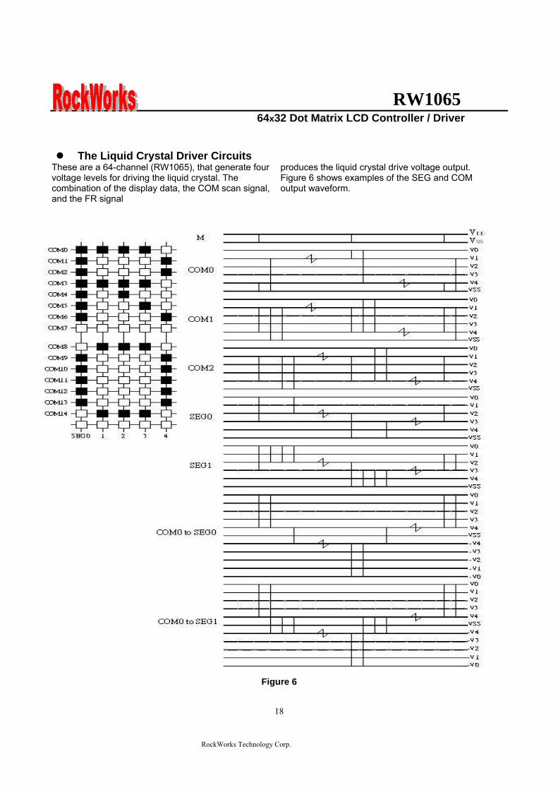
RW1065 64x32 Dot Matrix LCD Controller Driver
RockWorks Technology Corp
18
The Liquid Crystal Driver Circuits
These are a 64-channel (RW1065) that generate four voltage levels for driving the liquid crystal The combination of the display data the COM scan signal and the FR signal
produces the liquid crystal drive voltage output Figure 6 shows examples of the SEG and COM output waveform
Figure 6
RW1065 64x32 Dot Matrix LCD Controller Driver
RockWorks Technology Corp
19
The Power Supply Circuit
The power supply circuits are low-power consumption power supply circuits that generate the voltage levels required for the liquid crystal drivers They comprise Booster circuits and voltage follower circuits They are only enabled in master operation The power supply circuits can turn on automatically after power on
Consequently it is possible to make an external power supply and the internal power supply function somewhat in parallel
The Liquid Crystal Voltage Generator Circuit The V0 voltage is produced by a resistive voltage divider outside the IC through VRAB pin and can be produced at the V1 V2 V3 and V4 voltage levels required for liquid crystal driving Moreover when the voltage follower changes the impedance it provides V1 V2 V3 and V4 to the liquid crystal drive circuit 15 bias or 16 bias or 18 bias or 19 bias for RW1065 can be selected by BS0 and BS1 pins V0-Vss maximum voltage is 15V Vout-Vss maximum voltage is 17V If VDD lt 35V it can use the Booster circuit 2x3x4xThe booster voltage can follow the spec condition (Vout-Vss ≦ 17V max voltage) if VDD gt35V only use the 2X3X booster circuit that can ensure the V0-Vss voltage ≦ 15V If use the VDD voltage 5V and 4X booster itrsquos over the spec operation condition To turn on built-in power (boosterfollower) must waiting 200mS to display on for boosterfollower stable Therefore power off must follower ldquopower off sequencerdquo too
Power on Display off
Power off
Power off sequence
Wait time gt200mS
Display on
Power on sequence
RW1065 64x32 Dot Matrix LCD Controller Driver
RockWorks Technology Corp
20
The Reset Circuit
When the RTP input comes to the ldquoLrdquo level these LSIs return to the default state Their default states are as follows 1 Display OFF 2 Display all point on is select to normal 3 Display normalreverse is select to normal 4 164 duty is selected 5 Read modify write OFF 6 Column address set to Address 0 7 Page address set to Page 0 8 Start line set to first line 9 Frame frequency set to default 10 Power save mode released 11 Ext set to ldquo0rdquo When the power is turned on the IC internal state becomes unstable and it is necessary to initialize it using the RSTP terminal After the initialization each input terminal should be controlled normally While RSTP is ldquoLrdquo the oscillator works but the display timing generator stops and the CL FR terminals are fixed to ldquoHrdquo The terminals D0 to D7 are not affected
RW1065 64x32 Dot Matrix LCD Controller Driver
RockWorks Technology Corp
21
TABLE OF RW1065 INSTRUCTIONS
Instruction code Instruction RS RW DB7 DB6 DB5 DB4 DB3 DB2 DB1 DB0 Description
EXT=0 or 1
MODE SET 0 0 0 0 0 0 1 1 0 EXT Set EXT mode
Instruction code Instruction RS RW DB7 DB6 DB5 DB4 DB3 DB2 DB1 DB0 Description
EXT=0 Display ONOFF 0 0 0 0 1 1 1 1 1 D D=0Display OFF
D=1Display ONSet page address 0 0 1 0 1 1 1 P2 P1 P0 Set page address
Set column address 0 0 0 1 Y5 Y4 Y3 Y2 Y1 Y0 Set column
address MSB
Read Status 0 1 BUSY 0 ON OFF RESET 0 0 0 0 Read register
status Write display
data 1 0 Write data Write data into DDRAM
Read display data 1 1 Read data Read data from
DDRAM Set initial
display line register
0 0 1 1 S5 S4 S3 S2 S1 S0 Specify the initial
display line to realize vertical scrolling
Instruction code Instruction RS RW DB7 DB6 DB5 DB4 DB3 DB2 DB1 DB0 Description
EXT=1
NOP 0 0 0 0 0 0 0 0 0 0 no operation
Set modiy-read 0 0 0 0 0 0 1 0 0 0 Set modiy-read
mode
END 0 0 0 0 0 0 1 1 1 0 release modiy-read mode
Set power save mode 0 0 0 0 0 0 0 0 1 PSAVE P=0 normal mode
P=1 sleep mode
0 0 0 0 0 1 0 1 Display
COMMAND (double
command)
0 0 FRSEL
0 0 0 0 REV ALLON DUTY
DUTY=1 64 duty DUTY=0 32 duty ALLON=1display all on ALLON=0display
normal REV=1display reverse REV=0display normal FRSEL=1FR frequency double default FRSEL=0FR frequency default
RW1065 64x32 Dot Matrix LCD Controller Driver
RockWorks Technology Corp
22
Command Description
See the Table of RW1065 instructions The RW1065 series identifies a data bus using a combination of RS E and RW signals As the MPU translates a command in the internal timing only (independent from the external clock) its speed is very high The busy check is usually not required
Display ONOFF
EXT RS RW D7 D6 D5 D4 D3 D2 D1 D0
0 0 0 0 0 1 1 1 1 1 D
This command turns the display on and off D=1 Display ON D=0 Display OFF(default)
Set page Address This command specifies the page address that corresponds to the low address of the display data RAM when it is accessed by the MPU Any bit of the display data RAM can be accessed when its page address and column address are specified The display status is not changed even when the page address is changed
EXT RS RW D7 D6 D5 D4 D3 D2 D1 D0
0 0 0 1 0 1 1 1 A2 A1 A0
This command loads the page address register
A2 A1 A0 Page
0 0 0 0 (default)
0 0 1 1 0 1 0 2 0 1 1 3 1 0 0 4 1 0 1 5 1 1 0 6 1 1 1 7
Page mapping see Figure 4
RW1065 64x32 Dot Matrix LCD Controller Driver
RockWorks Technology Corp
23
Set Column Address This command specifies a column address of the display data RAM When the display data RAM is accessed by the MPU continuously the column address is incremented by I each time it is accessed from the set address Therefore the MPU can access to data continuously The column address stops to be incremented at address 63 and the page address is not changed continuously
EXT RS RW D7 D6 D5 D4 D3 D2 D1 D0
0 0 0 0 1 A5 A4 A3 A2 A1 A0
A5 A4 A3 A2 A1 A0 Column Address0 0 0 0 0 0 0(default) 0 0 0 0 0 1 1
1 1 1 1 1 1 63
Read Status
EXT RS RW D7 D6 D5 D4 D3 D2 D1 D0
0 0 1 BUSY 0 ON OFF RESET 0 0 0 0
The BUSY Flag bit indicates that RW 1065 is operating or no operating
BUSY=1 Operation BUSY=0 Ready
The ONOFF bit indicates the current status of the display It is the inverse of the polarity of the display ONOFF command ONOFF=1 Display OFF ONOFF=0 Display ON The RESET bit indicates whether the driver is executing a hardware or software reset or if it is in normal operating mode RESET=1 Currently executing reset command RESET=0 Normal operation
RW1065 64x32 Dot Matrix LCD Controller Driver
RockWorks Technology Corp
24
Write Display Data
EXT RS RW D7 D6 D5 D4 D3 D2 D1 D0
0 1 0 Write data
Writes 8-bits of data into the display data RAM at a location specified by the contents of the column address and page address registers and then increments the column address register by one
Read Display Data
EXT RS RW D7 D6 D5 D4 D3 D2 D1 D0
0 1 1 Read data
Reads 8-bits of data from the data IO latch updates the contents of the IO latch with display data from the display data RAM location specified by the contents of the column address and page address registers and then increments the column address register After loading a new address into the column address register one dummy read is required before valid data is obtained
Set initial display line register
EXT RS RW D7 D6 D5 D4 D3 D2 D1 D0
0 0 0 1 1 S5 S4 S3 S2 S1 S0
Loads the RAM line address of the initial display line COM 0 into the initial display line register The RAM display data becomes the top line of the LCD screen It is followed by the higher number lines in ascending order corresponding to the duty cycle The screen can be scrolled using this command by incrementing the line address(default value=rdquo00Hrdquo)
RW1065 64x32 Dot Matrix LCD Controller Driver
RockWorks Technology Corp
25
Read-Modify-Write
EXT RS RW D7 D6 D5 D4 D3 D2 D1 D0
1 0 0 0 0 0 0 1 0 0 0
This command defeats column address register auto-increment after data reads The current contents of the column Address register are saved The mode remains active until an End command is received When the End command is entered the column address is returned to the one used during input of Read-Modify-Write Command This function can reduce the load of MPU when data change is repeated as a specific display area Any command other than Data Read or Write can be used in the Read-Modify-Write mode However the Column Address Set command cannot be used
End
EXT RS RW D7 D6 D5 D4 D3 D2 D1 D0
1 0 0 0 0 0 0 1 1 1 0
This command cancels read-modify-write mode and restores the contents of the column address register to their value prior to the receipt of the Read-Modify-Write command
N N+1 N+2 N+3 N+m N
Read -modify-write mode set End
Returm
Column address
Set page address
Set column address
Read-modify-write
Dummy read
Read data
Write data
End
CompletedNo
Yes
RW1065 64x32 Dot Matrix LCD Controller Driver
RockWorks Technology Corp
26
Set power save mode
EXT RS RW D7 D6 D5 D4 D3 D2 D1 D0
1 0 0 0 0 0 0 0 0 1 PSAVE
When power save mode is entered thus greatly reducing power consumption In the power save mode the display data is saved as is the operating mode that was in effect before the power saver mode was initiated and the MPU is still able to access the display data RAM PSAVE=1 Sleep mode PSAVE=0 Normal mode Sleep mode This stops all operations in the LCD display system and as long as there are no accesses from the MPU the consumption current is reduced to a value near the static current The internal modes during sleep mode are as follows 1 The oscillator circuit and the LCD power supply circuit are halted 2 All liquid crystal drive circuits are halted and the segment and common drive outputs output a Vss level
Display command double command
EXT RS RW D7 D6 D5 D4 D3 D2 D1 D0
1 0 0 0 0 0 0 0 1 0 1
1 0 0 FRSEL 0 0 0 0 REV ALLON DUTY
Display NormalReverse set REV=1 Reverse REV=0 Normal(default) Display All Point ONOFF ALLON=1 All display points ON ALLON=0 Normal(default) Select Duty Duty=1 164 duty cycle(default) Duty=0 132 duty cycle FRAME FREQUENCY Select FRSEL=1 Double FRSEL=0 (default)
RW1065 64x32 Dot Matrix LCD Controller Driver
RockWorks Technology Corp
27
Hardware Pin Set
Select ADC by ADC Pin The pin selects the relationship between display data RAM column addresses and segment drivers ADC=1 SEG0larrcolumn address 3FHhellipinverted ADC=0 SEG0larrcolumn address 00Hhellipnormal(default) This command is provided to reduce restrictions on the placement of driver ICs and routing of traces during printed circuit Board design See Figure 4 for a table of segments and column addresses for the two values of D
Select SHL by SHL Pin The pin selects the com output scan direction SHL=1 Reverse directioncom63rarrcom0 SHL=0 Normal com0rarrcom63 Both master and slave should set identical SHL value
Select LCD Bias by BS0 BS1 Pin
BS1 BS0 Bias 0 0 15 bias 0 1 16 bias 1 0 18 bias 1 1 19 bias
RW1065 64x32 Dot Matrix LCD Controller Driver
RockWorks Technology Corp
28
When an External Resistance is Used The liquid crystal power supply voltage V0 is set by adding resistors Rarsquo and Rbrsquo between VDD and VR and between VR and V0 respectively
RW1065
RW1065 64x32 Dot Matrix LCD Controller Driver
RockWorks Technology Corp
29
The set voltage circuits
Using the step-up voltage circuits equipped within the RW1065 chips it is possible to produce a 2X 3X 4X step-up voltage levels 2X step-up
To produce voltage level in the positive direction at the Vout terminal that is 2 times the voltage difference between VSS and VDD2 Please configure set voltage circuits like this Place a 1uF~22uF capacitor between CAP1N and CAP1P Place a 1uF~22uF capacitor between VSS and VOUT Short CAP2P CAP3P and VOUT Leave CAP2N open 3X step-up
To produce voltage level in the positive direction at the Vout terminal that is 3 times the voltage difference between VSS and VDD2 Please configure set voltage circuits like this Place a 1uF~22uF capacitor between CAP1N and CAP1P Place a 1uF~22uF capacitor between VSS and VOUT Place a 1uF~22uF capacitor and 100 ohms resistor between CAP2N and CAP2P Short CAP3P and Vout 4X step-up
To produce voltage level in the positive direction at the Vout terminal that is 4 times the voltage difference between VSS and VDD2 Please configure set voltage circuits like this Place a 1uF~22uF capacitor between CAP1N and CAP1P Place a 1uF~22uF capacitor between VSS and VOUT Place a 1uF~22uF capacitor and 100 ohms resistor between CAP2N and CAP2P Place a 1uF~22uF capacitor and 100 ohms resistor between CAP1N and CAP3P
RW1065 64x32 Dot Matrix LCD Controller Driver
RockWorks Technology Corp
30
ABSOLUTE MAXIMUM RATINGS Characteristics Symbol Value Unit
Power supply voltage VDD -03 to +70 V
LCD driver voltage Vout 0 to +17 V
Input voltage VIN -03 to VDD+03 V
Operating temperature TA -40 to +85
Storage temperature TSTO -55 to +125
DC CHARACTERISTICS
Rating Item Symbol Condition Min Typ Max Unit ApplicablePin
Operating Voltage VDD - 27 30 55 V VDD1
Step up output voltage Vout (Relative to VDD) 0 - 17 V Vout
Voltage follower circuit operating Voltage V0 (Relative to VDD) 0 - 15 V V0
V0 accuracy V0 - 0 - 15 V0
High-level Input Voltage Low-level Input Voltage
VIHC VILC - 07 VDD
Vss - VDD 09 V 2
High-level Output Voltage Low-level Output Voltage
VOHC VOLC
IOH = ndash05 mA IOL = 05 mA
08VDD Vss - VDD
02 VDD V 3
Input leakage current ILI VIN = VDD or VSS -1 - 2 uA 4
Output leakage current ILO - -1 1 uA 5
Liquid Crystal Driver ON Resistance RON
Ta= 25degC(Relative To VDD)
V0 =15 V - 16 20 KΩ SEGn COMn 6
Internal Oscillator fOSC 2286 254 2794 Oscillator
Frequency External Input RECOMMAND fCL
Ta = 25degC 132Duty 2286 254 2794
kHz CL
Internal Oscillator fOSC 45 5 55 Oscillator
Frequency External Input RECOMMAND fCL
Ta = 25degC 164Duty 45 5 55
kHz CL
bullDynamic Consumption Current During Display with the Internal Power Supply OFF Current consumed by total ICs when an external power supply is used
Unless otherwise specified Vss=0V VDD=30V
RW1065 64x32 Dot Matrix LCD Controller Driver
RockWorks Technology Corp
31
Display Pattern OFF
Ta = 25degC Vout=17V Rating Item Symbol Condition Min Typ Max Unit Notes
VDD=30 V V0-Vss=8V - 10 15 RW1065 IDD VDD=50 V V0-Vss=8V - 35 45
microA 7
Display Pattern Checker
Ta = 25degC Vout=17V Rating Item Symbol Condition Min Typ Max Unit Notes
VDD=30 V V0-Vss=8V - 15 20 RW1065 IDD VDD=50 V V0-Vss=8V - 40 50
microA 7
Display Pattern OFF
Ta = 25degC Vout=17V Rating Item Symbol Condition Min Typ Max Unit Notes
VDD=30 V V0-Vss=8V - 15 20 RW1065 IDD VDD=50 V V0-Vss=8V - 40 50
microA 7
Display pattern Checker
Ta = 25degC Vout=17V Rating Item Symbol Condition Min Typ Max Unit Notes
VDD=30 V V0-Vss=8V - 65 80 RW1065 IDD VDD=50 V V0-Vss=8V - 130 150
microA 7
bull Consumption Current at Time of Power Saver Mode VSS = 0 V VDD = 30 V plusmn 10
Rating Item Symbol Condition Min Typ Max Unit Notes
Sleep mode IDD - - 5 10 microA -
References for items market with 1 While a broad range of operating voltages is guaranteed performance cannot be guaranteed if there are sudden fluctuations to the
voltage while the MPU is being accessed 2 The RS D0 to D5 D6 D7 E RW CS1BP CS2P CLS CL FR MS and RST
― terminals
3 The D0 to D7 FR and CL terminals 4 The RS E RW CS1BP CS2P CLS MS and RST
― terminals
5 Applies when the D0 to D5 D6 D7 CL and FR terminals are in a high impedance state 6 These are the resistance values for when a 01 V voltage is applied between the output terminals SEGn or COMn and
the various power supply terminals (V1 V2 V3 and V4) These are specified for the operating voltage (3) range RON = 01 V ∆I (Where ∆I is the current that flows when 01 V is applied while the power supply is ON)
7 It indicates the current consumed on ICs alone when the internal oscillator circuit and display are turned on Does not include the current due to the LCD panel capacity and wiring capacity Applicable only when there is no access from the MPU
RW1065 64x32 Dot Matrix LCD Controller Driver
RockWorks Technology Corp
32
TIMING CHARACTERISTICS
68 Interface
(Ta=-40 to 85 degC) VDD=27 to 45V
Rating VDD=45 to 55V
Rating Item Signal Symbol ConditionMin Max Min Max
Units
Address hold time RS tAH6 0 mdash 0 mdash Address setup time RS tAW6
mdash 0 mdash 0 mdash
ns
System cycle time RS tCYC6 mdash 900 mdash 800 mdash ns Data setup time D0 to D7 tDS6 100 mdash 100 mdash Data hold time D0 to D7 tDH6
mdash 0 mdash 0 mdash
ns
Access time D0 to D7 tACC6 mdash 350 mdash 250
Output disable time D0 to D7 tOH6 CL = 100 pF
mdash 300 mdash 200 ns
Read tEWHR 360 mdash 300 mdash Enable H pulse time
WriteE
tEWHW mdash
360 mdash 300 mdash ns
Read tEWLR 450 mdash 400 mdash Enable L pulse time
WriteE
tEWLW mdash
450 mdash 400 mdash ns
1 All timing is specified using 20 and 80 of VDD as the reference 2 tEWLW and tEWLR are specified as the overlap between CS1BP being ldquoLrdquo (CS2P = ldquoHrdquo) and E
RW1065 64x32 Dot Matrix LCD Controller Driver
RockWorks Technology Corp
33
Reset Timing
Rating Item Signal Symbol Condition
Min Typ Max Units
Reset time mdash tR mdash mdash - 2 micros
Reset ldquoLrdquo pulse width RST tRW mdash 2 - mdash micros
1 When double chip was be used then the duty set command must be set between the tR
RW1065 64x32 Dot Matrix LCD Controller Driver
RockWorks Technology Corp
34
IO PAD CONFIGURATION
RW1065 64x32 Dot Matrix LCD Controller Driver
RockWorks Technology Corp
35
THE MPU INTERFACE (REFERENCE EXAMPLES) The RW1065 Series can be connected to 6800 Series MPUs The display area can be enlarged by using multiple RW1065 Series chips When this is done the chip select signal can be used to select the individual ICs to access
6800 Series MPUs
RW
106
5
RW1065 64x32 Dot Matrix LCD Controller Driver
RockWorks Technology Corp
36
When using external multi-level power supply for LCD driving (REFERENCE EXAMPLE)
Using a resistor divider can provide RW1065 external multi-level power supply for LCD driving
The circuit below shows a resistor divider network which can bias V0 V1 V2 V3 and V4 externally
RW1065 64x32 Dot Matrix LCD Controller Driver
RockWorks Technology Corp
37
bullWhen V0 V1 V2 V3 and V4 are biased by external power supply analog section of RW1065 should be turn off by software during LCD initialization The example in below shows the sequence to turn off analog section when external bias is used Begin of LCD initialization 1 Reset RW1065 2 SET EXT=1 (mode instruction)
RS RW DB7 DB6 DB5 DB4 DB3 DB2 DB1 DB00 0 0 0 0 0 1 1 0 1
3 SET Display Command (double command)
RS RW DB7 DB6 DB5 DB4 DB3 DB2 DB1 DB00 0 0 0 0 0 0 1 0 1 0 0 0 0 1 1 0 0 0 1
4 SET EXT=1 (mode instruction)
RS RW DB7 DB6 DB5 DB4 DB3 DB2 DB1 DB00 0 0 0 0 0 1 1 0 0
End of LCD initialization
bullBecause pins can not set LCD bias when external power supplies are used for LCD driving the bias can be set by an appropriate configuration for a resistor voltage divider networks The example is shown below
VSS
R
R
NR
R
R
RV1
RV2
RV3
RV4
V0
Bias Network Circuit Concept 15 Bias N=1 total = 5R 16 Bias N=2 total =6R 18 Bias N=4 total =8R 19 Bias N=5 total = 9R
RW1065 64x32 Dot Matrix LCD Controller Driver
RockWorks Technology Corp
38
Single chip solution for RW1065 application (REFERENCE EXAMPLE)
For a 64x32 application the duty cycle of LCD panel is 164 and the display duty of RW1065 should be set to 164 The display duty cycle can be selected by the DUTY bit in display command The diagram for 64x32 application is shown below
64 SEGx32COM LCD Panel
164 duty cycle
RW1065 DUTY=1
COM1~33
SEG1~65
RW1065 64x32 Dot Matrix LCD Controller Driver
RockWorks Technology Corp
39
Using an adjustable resistor on the main board to adjust the contrast of liquid crystal display (REFERENCE EXAMPLE)
The schematic shows an adjustable resistor on main board that can adjust voltage level of V0
RW1065 64x32 Dot Matrix LCD Controller Driver
RockWorks Technology Corp
40
Package information (Please pay close attention to the information in this section Do not hesitate to consult with our sale representative if you have any question or concern)
In order to make better bonding yield for RW1065 please follow the tips and recommendations in this section In this section few tips about COB footprint style PCB layout and wire bonding will be discussed
The drawing in below shows the PCB footprint style which we recommend for RW1065 Pads array in
curve shape is easier for Al wire bonding Besides that a real size COB footprint for RW1065 is also shown in below RW1065 COB footprint is also available in powerpcb or protel format for design reference purpose
The ratio is 11
RW1065 64x32 Dot Matrix LCD Controller Driver
RockWorks Technology Corp
41
During COB footprint design there have some tips about footprint that the PCB designer should know The angle between bonding wire and vertical line should less than 45 Otherwise the wire shorts would become very easy to happen at fours corners of the chip
The angle between bonding wire and vertical line could be reduced by expanding the distance between pads array and the chip In addition reducing length in horizon direction of pads array could minimize the angle between bonding wire and vertical line The picture in below will help to illustrate this concept From the experiences COB footprint style affects the bonding yield
Bad Wires are too close to each other
The angle between bonding wire and vertical line is greater than 45
The angle between bonding wire and vertical line is less than 45
Wires are not too close to each other
Reducing length in horizon direction of pads array could minimize the angle between bonding wire and vertical line
The angle between bonding wire and vertical line could be reduced by expanding the distance between pads array and the chip
RW1065 64x32 Dot Matrix LCD Controller Driver
RockWorks Technology Corp
42
If the gap between pads of COB footprint is filled with solder mask coating it is difficult to bond Al wire to
the pads The top solder masks layer that overlap COB footprint area should be removed
Please use 1 mils diameter Al wire for RW1065 wire bonding
1 2 3 4 5 6
A
B
C
D
654321
D
C
B
A
Title
Number RevisionSize
C
Date 29-Aug-2007 Sheet of File D公司資料99seMyDesignddb Drawn By
RW1065
COM131
COM142
COM153
COM164
COM175
COM186
COM197
COM208
COM219
COM2210
COM2311
COM2412
COM2513
COM2614
COM2715
COM2816
COM2917
COM3018
COM3119
SEG
6320
SEG
6221
SEG
6122
SEG
6023
SEG
5924
SEG
5825
SEG
5726
SEG
5627
SEG
5528
SEG
5429
SEG
5330
SEG
5231
SEG
5132
SEG
5033
SEG
4934
SEG
4835
SEG
4736
SEG
4637
SEG
4538
SEG
4439
SEG
4340
SEG
4241
SEG
4142
SEG
4043
SEG
3944
SEG
3845
SEG
3746
SEG
3647
SEG
3548
SEG
3449
SEG
3350
SEG
3251
SEG
3152
SEG
3053
SEG
2954
SEG
2855
SEG
2756
SEG
2657
SEG
2558
SEG
2459
SEG
2360
SEG
2261
SEG
2162
SEG
2063
SEG
1964
SEG
1865
SEG
1766
SEG
1667
SEG
1568
SEG
1469
SEG13 70SEG12 71SEG11 72SEG10 73SEG9 74SEG8 75SEG7 76SEG6 77SEG5 78SEG4 79SEG3 80SEG2 81SEG1 82SEG0 83ADCP 84CLL 85
VSS
86D
087
D1
88D
289
D3
90D
491
D5
92D
693
D7
94C
S1B
P95
CS2
P96
ERD
P97
AO
P(R
S)98
RW
RP
99V
DD
100
RST
P10
1C
LSP
102
FRR
103
MSP
104
BS1
P10
5B
S0P
106
SHLP
107
VD
D2
108
CA
P2N
109
CA
P2P
110
CA
P1P
111
CA
P1N
112
CA
P3P
113
VO
UT
114
V0
115
VR
AB
116
V3
117
V2
118
V4
119
V1
120
CO
M0
121
CO
M1
122
CO
M2
123
CO
M3
124
CO
M4
125
CO
M5
126
CO
M6
127
CO
M7
128
CO
M8
129
CO
M9
130
CO
M10
131
CO
M11
132
CO
M12
133
4897x1902 um
IC1
RW1065
C9CAPR4
100R0603
R30R0603
C8
CAP
C7
CAP
R2
100R0603
R1
0R0603C6 22uf
R50R
R6300R
R7RES1
R8NC R9
100R0603
VDD
R10
NC
R11
100R0603
R12
100R0603
R13
NC
R14
100R0603
R15
NC
VDD
D0
D1
D2
D3
D4
D5
D6
D7
DB[07]
VDDC5
01uf0603
VD
D
CS2
P
123456789
1011121314151617181920
J1
CON20
C1201uf0603
R3951K0603
VDD
CAP Value1UF~22UF
2XPut C6C8 Short R1R3Open R2R4C7C93XPut C6C8C9 R4Short R1Open R2R3C74XOpen R1R3
BS0 BS1 Bias0 0
0 1
1 0
11
15 bias
16 bias
18 bias
19 bias
ADC=0 SEG0lt~column address 00Hnormal(default) ADC=1 SEG0lt~column address 3FHinverted
SHL=0 Normal COM0~gtCOM63(default)SHL=1 Reverse direction COM63~gtCOM0
R16100R0603
LCD PANEL 64X32RockWorks
RW1065 64X32
COM0-31 SEG0-63SHL=0 ADC=0
SHL=1COM31-0
ADC=1SEG63-0
if use single chip for 32 command displaythe display command must select 164 dutyDisplay panel must select 164 duty type
VO
UT
C3P
C1N
C1P
C2P
C2N
VDD2
ADC
SHL
BS0
BS1
CLLADC
V1
V2
V3
V4
VR
AB
V0
VO
UT
C3P
C1N
C1P
C2P
C2N
VD
D2
SHL
BS0
BS1
FRR
RST
P
RW
RS
E CS1
B
CS1
V0RSRWED0D1D2D3D4D5D6D7
RSTPAK
C4
22uf
RBRES1
RA1RES1
C2
22uf
C1
22uf
C3
22uf
C0
22uf
R20
100k0603
R21
100k0603
R17
200K0603
V1
V2
V3
V4 VRAB
V0
V0
OPTION
B
R18
300R0603
RA2RES1
VADJ
R19100R
R23 RES1R22 0R
R24
RES1
R25
0R
VDD
CS1BP
CS2P
CS1
CS1
R26
22R0603
R27
22R0603
C1047uf
C11
01uf
VSS_INVDD_IN
D1DIODE
FGND
鐵框地
VSS
VDD
R28 10RR29 10RR30 10RR31 10RR32 10RR33 10RR34 10RR35 10RR36 10RR37 10RR38 10R
VADJ
1 2 3 4 5 6
A
B
C
D
654321
D
C
B
A
Title
Number RevisionSize
C
Date 29-Aug-2007 Sheet of File D公司資料99seMyDesignddb Drawn By
RW1065
COM131
COM142
COM153
COM164
COM175
COM186
COM197
COM208
COM219
COM2210
COM2311
COM2412
COM2513
COM2614
COM2715
COM2816
COM2917
COM3018
COM3119
SEG
6320
SEG
6221
SEG
6122
SEG
6023
SEG
5924
SEG
5825
SEG
5726
SEG
5627
SEG
5528
SEG
5429
SEG
5330
SEG
5231
SEG
5132
SEG
5033
SEG
4934
SEG
4835
SEG
4736
SEG
4637
SEG
4538
SEG
4439
SEG
4340
SEG
4241
SEG
4142
SEG
4043
SEG
3944
SEG
3845
SEG
3746
SEG
3647
SEG
3548
SEG
3449
SEG
3350
SEG
3251
SEG
3152
SEG
3053
SEG
2954
SEG
2855
SEG
2756
SEG
2657
SEG
2558
SEG
2459
SEG
2360
SEG
2261
SEG
2162
SEG
2063
SEG
1964
SEG
1865
SEG
1766
SEG
1667
SEG
1568
SEG
1469
SEG13 70SEG12 71SEG11 72SEG10 73SEG9 74SEG8 75SEG7 76SEG6 77SEG5 78SEG4 79SEG3 80SEG2 81SEG1 82SEG0 83ADCP 84CLL 85
VSS
86D
087
D1
88D
289
D3
90D
491
D5
92D
693
D7
94C
S1B
P95
CS2
P96
ERD
P97
AO
P(R
S)98
RW
RP
99V
DD
100
RST
P10
1C
LSP
102
FRR
103
MSP
104
BS1
P10
5B
S0P
106
SHLP
107
VD
D2
108
CA
P2N
109
CA
P2P
110
CA
P1P
111
CA
P1N
112
CA
P3P
113
VO
UT
114
V0
115
VR
AB
116
V3
117
V2
118
V4
119
V1
120
CO
M0
121
CO
M1
122
CO
M2
123
CO
M3
124
CO
M4
125
CO
M5
126
CO
M6
127
CO
M7
128
CO
M8
129
CO
M9
130
CO
M10
131
CO
M11
132
CO
M12
133
4897x1902 um
IC1
RW1065 Master
RW1065
COM131
COM142
COM153
COM164
COM175
COM186
COM197
COM208
COM219
COM2210
COM2311
COM2412
COM2513
COM2614
COM2715
COM2816
COM2917
COM3018
COM3119
SEG
6320
SEG
6221
SEG
6122
SEG
6023
SEG
5924
SEG
5825
SEG
5726
SEG
5627
SEG
5528
SEG
5429
SEG
5330
SEG
5231
SEG
5132
SEG
5033
SEG
4934
SEG
4835
SEG
4736
SEG
4637
SEG
4538
SEG
4439
SEG
4340
SEG
4241
SEG
4142
SEG
4043
SEG
3944
SEG
3845
SEG
3746
SEG
3647
SEG
3548
SEG
3449
SEG
3350
SEG
3251
SEG
3152
SEG
3053
SEG
2954
SEG
2855
SEG
2756
SEG
2657
SEG
2558
SEG
2459
SEG
2360
SEG
2261
SEG
2162
SEG
2063
SEG
1964
SEG
1865
SEG
1766
SEG
1667
SEG
1568
SEG
1469
SEG13 70SEG12 71SEG11 72SEG10 73SEG9 74SEG8 75SEG7 76SEG6 77SEG5 78SEG4 79SEG3 80SEG2 81SEG1 82SEG0 83ADCP 84CLL 85
VSS
86D
087
D1
88D
289
D3
90D
491
D5
92D
693
D7
94C
S1B
P95
CS2
P96
ERD
P97
AO
P(R
S)98
RW
RP
99V
DD
100
RST
P10
1C
LSP
102
FRR
103
MSP
104
BS1
P10
5B
S0P
106
SHLP
107
VD
D2
108
CA
P2N
109
CA
P2P
110
CA
P1P
111
CA
P1N
112
CA
P3P
113
VO
UT
114
V0
115
VR
AB
116
V3
117
V2
118
V4
119
V1
120
CO
M0
121
CO
M1
122
CO
M2
123
CO
M3
124
CO
M4
125
CO
M5
126
CO
M6
127
CO
M7
128
CO
M8
129
CO
M9
130
CO
M10
131
CO
M11
132
CO
M12
133
4897x1902 um
IC2
RW1065 Slave
C4
22uf
RBRES1
RA1RES1
C2
22uf
C1
22uf
C3
22uf
C0
22ufC9CAPR4
100R0603
R30R0603
C8
CAP
C7
CAP
R2
100R0603
R1
0R0603C6 22uf
R50R0603
R6300R0603
R7RES1
R8NC R9
100R0603
VDD
R10
NC
R11
100R0603
R12
NC
R13
100R0603
R14
100R0603
R15
NC
R16
100R0603
R17
NC
VDD
D0
D1
D2
D3
D4
D5
D6
D7
D0
D1
D2
D3
D4
D5
D6
D7
DB[07] DB[07]
VDDC10
01uf0603
VD
D
IC1_
CS2
P
VDD
IC2_
CS2
P
VD
D
C11
01uf0603
VSS
VSS
LCD PANEL 128X64
Master COM0-31 Slave COM32-63
Master SEG0-63 Slave SEG64-127
123456789
1011121314151617181920
J1
CON20
Master Slave
CAP Value1UF~22UF
2XPut C6C8 Short R1R3Open R2R4C7C93XPut C6C8C9 R4Short R1Open R2R3C74XOpen R1R3
RockWorksRW1065 128x64
BS0 BS1 Bias0 0
0 1
1 0
11
15 bias
16 bias
18 bias
19 bias
ADC=0 SEG0lt~column address 00Hnormal(default) ADC=1 SEG0lt~column address 3FHinverted
SHL=0 Normal COM0~gtCOM63(default)SHL=1 Reverse direction COM63~gtCOM0Both Master and Slave should set identical SHL value
SHL=0 SHL=0
ADC=0 ADC=0
Slave COM31-0
Slave SEG127-64
SHL=1
ADC=1
SHL=1Master COM63-32
ADC=1Master SEG63-0
R18100R0603
R22
100k0603
R23
100k0603
C501uF0603
R4551K0603
VDD
R19
200K0603
ADC1
ADC2
SHL
BS0
BS1
VDD2
V1
V2
V3
V4 VRAB
V0
V0V
OU
T
C3P
C1N
C1P
C2P
C2N
V1
V2
V3
V4
VR
AB
V0
VO
UT
C3P
C1N
C1P
C2P
C2N
VD
D2
SHL
BS0
BS1
FRR
RST
P
RW
RS
E IC1_
CS1
BP
V1
V2
V3
V4
VR
AB
V0
VO
UT
VD
D2
SHL
BS0
BS1
FRR
RST
P
RW
RS
E IC2_
CS1
BP
CLLADC1
CLLADC2
RSTP
CS1CS2
V0RSRWED0D1D2D3D4D5D6D7
AK
OPTION
R20
300R0603
RA2RES1
VADJ
R21
100R
B
R25 RESR24 0R
R26 RES R27 0RVDD
IC1_CS1BP
IC1_CS2P
CS1
CS1
R28 0R R29 RES
R30 RES R31 0R
IC2_CS1BP
IC2_CS2P
CS2
CS2
R32
22R0603
R33
22R0603
C1001uf
C11
47uf
D1DIODE
FGND
鐵框地
VSS
VDD
R34 10RR35 10RR36 10RR37 10RR38 10RR39 10RR40 10RR41 10RR42 10RR43 10RR44 10R
VSS_INVDD_IN
VADJ
VDD
1 2 3 4 5 6 7 8
A
B
C
D
87654321
D
C
B
A
Title
Number RevisionSize
D
Date 29-Aug-2007 Sheet of File D公司資料 99seMyDesignddb Drawn By
C422uf
RBRES1
RA1RES1
C3
22uf
C2
22uf
C1
22uf
C0
22ufC9CAPR4
100R0603
R30R0603
C8
CAP
C7
CAP
R2
100R0603
R1
0R0603C6 22uf
R220R0603
R23300R0603
R24RES1
R39
NCR40
100 ohm0603
VDD
R41
NC
R42
100 ohm0603
R43
NC
R44
100 ohm0603
R45
NC
R46
100 ohm0603
R47
100 ohm0603
R48
NC
R49
100 ohm0603
R50
NC
VDDCAP Value1UF~22UF
2XPut C6C8 Short R1R3Open R2R4C7C93XPut C6C8C9 R4Short R1Open R2R3C74XOpen R1R3
BS0 BS1 Bias0 0
0 1
1 0
11
15 bias
16 bias
18 bias
19 bias
ADC=0 SEG0lt~column address 00Hnormal(default)
ADC=1 SEG0lt~column address 3FHinverted
SHL=0 Normal COM0~gtCOM63(default)SHL=1 Reverse direction COM63~gtCOM0Both Master and Slave should set identical SHL value
R7
100k0603
R8
100k0603
V1
V2
V3
V4
V0
VRAB
V0
R5
200K
VDD2
VO
UT
C3P
C1N
C1P
C2P
C2N
ADC1
ADC2
ADC3
SHL
BS0
BS1
CS1CS2CS3
V0RSRWED0D1D2D3D4D5D6D7
RSTP
R3851K0603
C5
01uF
VDD
OPTION
R6
300R0603R9100R
RA2RES1
VADJ
RW1065
COM131
COM142
COM153
COM164
COM175
COM186
COM197
COM208
COM219
COM2210
COM2311
COM2412
COM2513
COM2614
COM2715
COM2816
COM2917
COM3018
COM3119
SEG
6320
SEG
6221
SEG
6122
SEG
6023
SEG
5924
SEG
5825
SEG
5726
SEG
5627
SEG
5528
SEG
5429
SEG
5330
SEG
5231
SEG
5132
SEG
5033
SEG
4934
SEG
4835
SEG
4736
SEG
4637
SEG
4538
SEG
4439
SEG
4340
SEG
4241
SEG
4142
SEG
4043
SEG
3944
SEG
3845
SEG
3746
SEG
3647
SEG
3548
SEG
3449
SEG
3350
SEG
3251
SEG
3152
SEG
3053
SEG
2954
SEG
2855
SEG
2756
SEG
2657
SEG
2558
SEG
2459
SEG
2360
SEG
2261
SEG
2162
SEG
2063
SEG
1964
SEG
1865
SEG
1766
SEG
1667
SEG
1568
SEG
1469
SEG13 70SEG12 71SEG11 72SEG10 73SEG9 74SEG8 75SEG7 76SEG6 77SEG5 78SEG4 79SEG3 80SEG2 81SEG1 82SEG0 83ADCP 84CLL 85
VSS
86D
087
D1
88D
289
D3
90D
491
D5
92D
693
D7
94C
S1B
P95
CS2
P96
ERD
P97
AO
P(R
S)98
RW
RP
99V
DD
100
RST
P10
1C
LSP
102
FRR
103
MSP
104
BS1
P10
5B
S0P
106
SHLP
107
VD
D2
108
CA
P2N
109
CA
P2P
110
CA
P1P
111
CA
P1N
112
CA
P3P
113
VO
UT
114
V0
115
VR
AB
116
V3
117
V2
118
V4
119
V1
120
CO
M0
121
CO
M1
122
CO
M2
123
CO
M3
124
CO
M4
125
CO
M5
126
CO
M6
127
CO
M7
128
CO
M8
129
CO
M9
130
CO
M10
131
CO
M11
132
CO
M12
133
4897x1902 um
IC1
RW1065 Master
RW1065
COM131
COM142
COM153
COM164
COM175
COM186
COM197
COM208
COM219
COM2210
COM2311
COM2412
COM2513
COM2614
COM2715
COM2816
COM2917
COM3018
COM3119
SEG
6320
SEG
6221
SEG
6122
SEG
6023
SEG
5924
SEG
5825
SEG
5726
SEG
5627
SEG
5528
SEG
5429
SEG
5330
SEG
5231
SEG
5132
SEG
5033
SEG
4934
SEG
4835
SEG
4736
SEG
4637
SEG
4538
SEG
4439
SEG
4340
SEG
4241
SEG
4142
SEG
4043
SEG
3944
SEG
3845
SEG
3746
SEG
3647
SEG
3548
SEG
3449
SEG
3350
SEG
3251
SEG
3152
SEG
3053
SEG
2954
SEG
2855
SEG
2756
SEG
2657
SEG
2558
SEG
2459
SEG
2360
SEG
2261
SEG
2162
SEG
2063
SEG
1964
SEG
1865
SEG
1766
SEG
1667
SEG
1568
SEG
1469
SEG13 70SEG12 71SEG11 72SEG10 73SEG9 74SEG8 75SEG7 76SEG6 77SEG5 78SEG4 79SEG3 80SEG2 81SEG1 82SEG0 83ADCP 84CLL 85
VSS
86D
087
D1
88D
289
D3
90D
491
D5
92D
693
D7
94C
S1B
P95
CS2
P96
ERD
P97
AO
P(R
S)98
RW
RP
99V
DD
100
RST
P10
1C
LSP
102
FRR
103
MSP
104
BS1
P10
5B
S0P
106
SHLP
107
VD
D2
108
CA
P2N
109
CA
P2P
110
CA
P1P
111
CA
P1N
112
CA
P3P
113
VO
UT
114
V0
115
VR
AB
116
V3
117
V2
118
V4
119
V1
120
CO
M0
121
CO
M1
122
CO
M2
123
CO
M3
124
CO
M4
125
CO
M5
126
CO
M6
127
CO
M7
128
CO
M8
129
CO
M9
130
CO
M10
131
CO
M11
132
CO
M12
133
4897x1902 um
IC2
RW1065 Slave
D0
D1
D2
D3
D4
D5
D6
D7
D0
D1
D2
D3
D4
D5
D6
D7
DB[07] DB[07]
VDDC8
01uf0603
VD
D
VDD
VD
D
C9
01uf0603
VSS
VSS
LCD PANEL 192X64
Master COM0-31 Slave COM32-63
Master SEG0-63 Slave SEG64-127
Master Slave
RockWorksRW1065 192x64
RW1065
COM131
COM142
COM153
COM164
COM175
COM186
COM197
COM208
COM219
COM2210
COM2311
COM2412
COM2513
COM2614
COM2715
COM2816
COM2917
COM3018
COM3119
SEG
6320
SEG
6221
SEG
6122
SEG
6023
SEG
5924
SEG
5825
SEG
5726
SEG
5627
SEG
5528
SEG
5429
SEG
5330
SEG
5231
SEG
5132
SEG
5033
SEG
4934
SEG
4835
SEG
4736
SEG
4637
SEG
4538
SEG
4439
SEG
4340
SEG
4241
SEG
4142
SEG
4043
SEG
3944
SEG
3845
SEG
3746
SEG
3647
SEG
3548
SEG
3449
SEG
3350
SEG
3251
SEG
3152
SEG
3053
SEG
2954
SEG
2855
SEG
2756
SEG
2657
SEG
2558
SEG
2459
SEG
2360
SEG
2261
SEG
2162
SEG
2063
SEG
1964
SEG
1865
SEG
1766
SEG
1667
SEG
1568
SEG
1469
SEG13 70SEG12 71SEG11 72SEG10 73SEG9 74SEG8 75SEG7 76SEG6 77SEG5 78SEG4 79SEG3 80SEG2 81SEG1 82SEG0 83ADCP 84CLL 85
VSS
86D
087
D1
88D
289
D3
90D
491
D5
92D
693
D7
94C
S1B
P95
CS2
P96
ERD
P97
AO
P(R
S)98
RW
RP
99V
DD
100
RST
P10
1C
LSP
102
FRR
103
MSP
104
BS1
P10
5B
S0P
106
SHLP
107
VD
D2
108
CA
P2N
109
CA
P2P
110
CA
P1P
111
CA
P1N
112
CA
P3P
113
VO
UT
114
V0
115
VR
AB
116
V3
117
V2
118
V4
119
V1
120
CO
M0
121
CO
M1
122
CO
M2
123
CO
M3
124
CO
M4
125
CO
M5
126
CO
M6
127
CO
M7
128
CO
M8
129
CO
M9
130
CO
M10
131
CO
M11
132
CO
M12
133
4897x1902 um
IC3
RW1065 Slave
D0
D1
D2
D3
D4
D5
D6
D7
DB[07]
VSS
VSS
VDD
VD
D
C10
01uf0603
Slave SEG128-192
Slave
SHL=0 SHL=0
Master COM63-32SHL=1 SHL=1
Slave COM31-0ADC=0 ADC=0 ADC=0
ADC=1 ADC=1 ADC=1Master SEG63-0 Slave SEG127-64 Slave SEG192-128
R50100R0603
V1
V2
V3
V4
VR
AB
V0
VO
UT
C3P
C1N
C1P
C2P
C2N
VD
D2
SHL
BS0
BS1
FRR
RST
P
RW
RS
E V1
V2
V3
V4
VR
AB
V0
VO
UT
VD
D2
SHL
BS0
BS1
FRR
RST
P
RW
RS
E V1
V2
V3
V4
VR
AB
V0
VO
UT
VD
D2
SHL
BS0
BS1
FRR
RST
P
RW
RS
E
CLL CLL CLLADC1 ADC2 ADC3
R25 10RR26 10RR27 10RR28 10RR29 10RR30 10RR31 10RR32 10RR33 10RR34 10RR35 10R
R36
22R0603
D1DIODE
R3722R0603
C647uf
C701uf
VSS_INVDD_IN
VSS
VDD
VADJ
123456789
101112131415161718192021222324
J1
CON24
AK
FGND
鐵框地
IC1_
CS1
BP
IC1_
CS2
P
IC2_
CS2
PIC
2_C
S1B
P
IC3_
CS1
BP
IC3_
CS2
B
R10 0R R11 RES
R12 RES R13 0RVDD
IC1_CS2B
IC1_CS1BPCS1
CS1
R14 0R R15 RES
R16 RES R17 0RVDDIC2_CS2B
IC2_CS1BPCS2
CS2
R18 0R R19 RES
R20 RES R21 0RVDDIC3_CS2B
IC3_CS1BPCS3
CS3
B
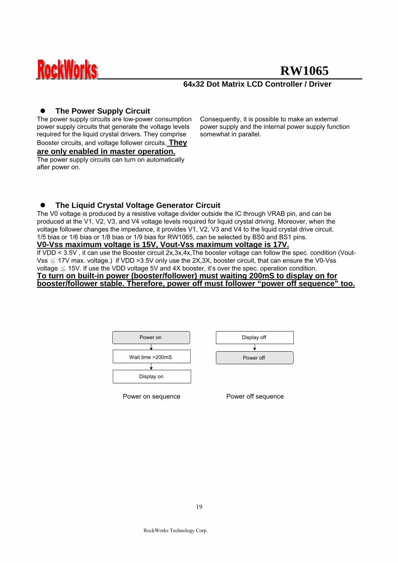
RW1065 64x32 Dot Matrix LCD Controller Driver
RockWorks Technology Corp
19
The Power Supply Circuit
The power supply circuits are low-power consumption power supply circuits that generate the voltage levels required for the liquid crystal drivers They comprise Booster circuits and voltage follower circuits They are only enabled in master operation The power supply circuits can turn on automatically after power on
Consequently it is possible to make an external power supply and the internal power supply function somewhat in parallel
The Liquid Crystal Voltage Generator Circuit The V0 voltage is produced by a resistive voltage divider outside the IC through VRAB pin and can be produced at the V1 V2 V3 and V4 voltage levels required for liquid crystal driving Moreover when the voltage follower changes the impedance it provides V1 V2 V3 and V4 to the liquid crystal drive circuit 15 bias or 16 bias or 18 bias or 19 bias for RW1065 can be selected by BS0 and BS1 pins V0-Vss maximum voltage is 15V Vout-Vss maximum voltage is 17V If VDD lt 35V it can use the Booster circuit 2x3x4xThe booster voltage can follow the spec condition (Vout-Vss ≦ 17V max voltage) if VDD gt35V only use the 2X3X booster circuit that can ensure the V0-Vss voltage ≦ 15V If use the VDD voltage 5V and 4X booster itrsquos over the spec operation condition To turn on built-in power (boosterfollower) must waiting 200mS to display on for boosterfollower stable Therefore power off must follower ldquopower off sequencerdquo too
Power on Display off
Power off
Power off sequence
Wait time gt200mS
Display on
Power on sequence
RW1065 64x32 Dot Matrix LCD Controller Driver
RockWorks Technology Corp
20
The Reset Circuit
When the RTP input comes to the ldquoLrdquo level these LSIs return to the default state Their default states are as follows 1 Display OFF 2 Display all point on is select to normal 3 Display normalreverse is select to normal 4 164 duty is selected 5 Read modify write OFF 6 Column address set to Address 0 7 Page address set to Page 0 8 Start line set to first line 9 Frame frequency set to default 10 Power save mode released 11 Ext set to ldquo0rdquo When the power is turned on the IC internal state becomes unstable and it is necessary to initialize it using the RSTP terminal After the initialization each input terminal should be controlled normally While RSTP is ldquoLrdquo the oscillator works but the display timing generator stops and the CL FR terminals are fixed to ldquoHrdquo The terminals D0 to D7 are not affected
RW1065 64x32 Dot Matrix LCD Controller Driver
RockWorks Technology Corp
21
TABLE OF RW1065 INSTRUCTIONS
Instruction code Instruction RS RW DB7 DB6 DB5 DB4 DB3 DB2 DB1 DB0 Description
EXT=0 or 1
MODE SET 0 0 0 0 0 0 1 1 0 EXT Set EXT mode
Instruction code Instruction RS RW DB7 DB6 DB5 DB4 DB3 DB2 DB1 DB0 Description
EXT=0 Display ONOFF 0 0 0 0 1 1 1 1 1 D D=0Display OFF
D=1Display ONSet page address 0 0 1 0 1 1 1 P2 P1 P0 Set page address
Set column address 0 0 0 1 Y5 Y4 Y3 Y2 Y1 Y0 Set column
address MSB
Read Status 0 1 BUSY 0 ON OFF RESET 0 0 0 0 Read register
status Write display
data 1 0 Write data Write data into DDRAM
Read display data 1 1 Read data Read data from
DDRAM Set initial
display line register
0 0 1 1 S5 S4 S3 S2 S1 S0 Specify the initial
display line to realize vertical scrolling
Instruction code Instruction RS RW DB7 DB6 DB5 DB4 DB3 DB2 DB1 DB0 Description
EXT=1
NOP 0 0 0 0 0 0 0 0 0 0 no operation
Set modiy-read 0 0 0 0 0 0 1 0 0 0 Set modiy-read
mode
END 0 0 0 0 0 0 1 1 1 0 release modiy-read mode
Set power save mode 0 0 0 0 0 0 0 0 1 PSAVE P=0 normal mode
P=1 sleep mode
0 0 0 0 0 1 0 1 Display
COMMAND (double
command)
0 0 FRSEL
0 0 0 0 REV ALLON DUTY
DUTY=1 64 duty DUTY=0 32 duty ALLON=1display all on ALLON=0display
normal REV=1display reverse REV=0display normal FRSEL=1FR frequency double default FRSEL=0FR frequency default
RW1065 64x32 Dot Matrix LCD Controller Driver
RockWorks Technology Corp
22
Command Description
See the Table of RW1065 instructions The RW1065 series identifies a data bus using a combination of RS E and RW signals As the MPU translates a command in the internal timing only (independent from the external clock) its speed is very high The busy check is usually not required
Display ONOFF
EXT RS RW D7 D6 D5 D4 D3 D2 D1 D0
0 0 0 0 0 1 1 1 1 1 D
This command turns the display on and off D=1 Display ON D=0 Display OFF(default)
Set page Address This command specifies the page address that corresponds to the low address of the display data RAM when it is accessed by the MPU Any bit of the display data RAM can be accessed when its page address and column address are specified The display status is not changed even when the page address is changed
EXT RS RW D7 D6 D5 D4 D3 D2 D1 D0
0 0 0 1 0 1 1 1 A2 A1 A0
This command loads the page address register
A2 A1 A0 Page
0 0 0 0 (default)
0 0 1 1 0 1 0 2 0 1 1 3 1 0 0 4 1 0 1 5 1 1 0 6 1 1 1 7
Page mapping see Figure 4
RW1065 64x32 Dot Matrix LCD Controller Driver
RockWorks Technology Corp
23
Set Column Address This command specifies a column address of the display data RAM When the display data RAM is accessed by the MPU continuously the column address is incremented by I each time it is accessed from the set address Therefore the MPU can access to data continuously The column address stops to be incremented at address 63 and the page address is not changed continuously
EXT RS RW D7 D6 D5 D4 D3 D2 D1 D0
0 0 0 0 1 A5 A4 A3 A2 A1 A0
A5 A4 A3 A2 A1 A0 Column Address0 0 0 0 0 0 0(default) 0 0 0 0 0 1 1
1 1 1 1 1 1 63
Read Status
EXT RS RW D7 D6 D5 D4 D3 D2 D1 D0
0 0 1 BUSY 0 ON OFF RESET 0 0 0 0
The BUSY Flag bit indicates that RW 1065 is operating or no operating
BUSY=1 Operation BUSY=0 Ready
The ONOFF bit indicates the current status of the display It is the inverse of the polarity of the display ONOFF command ONOFF=1 Display OFF ONOFF=0 Display ON The RESET bit indicates whether the driver is executing a hardware or software reset or if it is in normal operating mode RESET=1 Currently executing reset command RESET=0 Normal operation
RW1065 64x32 Dot Matrix LCD Controller Driver
RockWorks Technology Corp
24
Write Display Data
EXT RS RW D7 D6 D5 D4 D3 D2 D1 D0
0 1 0 Write data
Writes 8-bits of data into the display data RAM at a location specified by the contents of the column address and page address registers and then increments the column address register by one
Read Display Data
EXT RS RW D7 D6 D5 D4 D3 D2 D1 D0
0 1 1 Read data
Reads 8-bits of data from the data IO latch updates the contents of the IO latch with display data from the display data RAM location specified by the contents of the column address and page address registers and then increments the column address register After loading a new address into the column address register one dummy read is required before valid data is obtained
Set initial display line register
EXT RS RW D7 D6 D5 D4 D3 D2 D1 D0
0 0 0 1 1 S5 S4 S3 S2 S1 S0
Loads the RAM line address of the initial display line COM 0 into the initial display line register The RAM display data becomes the top line of the LCD screen It is followed by the higher number lines in ascending order corresponding to the duty cycle The screen can be scrolled using this command by incrementing the line address(default value=rdquo00Hrdquo)
RW1065 64x32 Dot Matrix LCD Controller Driver
RockWorks Technology Corp
25
Read-Modify-Write
EXT RS RW D7 D6 D5 D4 D3 D2 D1 D0
1 0 0 0 0 0 0 1 0 0 0
This command defeats column address register auto-increment after data reads The current contents of the column Address register are saved The mode remains active until an End command is received When the End command is entered the column address is returned to the one used during input of Read-Modify-Write Command This function can reduce the load of MPU when data change is repeated as a specific display area Any command other than Data Read or Write can be used in the Read-Modify-Write mode However the Column Address Set command cannot be used
End
EXT RS RW D7 D6 D5 D4 D3 D2 D1 D0
1 0 0 0 0 0 0 1 1 1 0
This command cancels read-modify-write mode and restores the contents of the column address register to their value prior to the receipt of the Read-Modify-Write command
N N+1 N+2 N+3 N+m N
Read -modify-write mode set End
Returm
Column address
Set page address
Set column address
Read-modify-write
Dummy read
Read data
Write data
End
CompletedNo
Yes
RW1065 64x32 Dot Matrix LCD Controller Driver
RockWorks Technology Corp
26
Set power save mode
EXT RS RW D7 D6 D5 D4 D3 D2 D1 D0
1 0 0 0 0 0 0 0 0 1 PSAVE
When power save mode is entered thus greatly reducing power consumption In the power save mode the display data is saved as is the operating mode that was in effect before the power saver mode was initiated and the MPU is still able to access the display data RAM PSAVE=1 Sleep mode PSAVE=0 Normal mode Sleep mode This stops all operations in the LCD display system and as long as there are no accesses from the MPU the consumption current is reduced to a value near the static current The internal modes during sleep mode are as follows 1 The oscillator circuit and the LCD power supply circuit are halted 2 All liquid crystal drive circuits are halted and the segment and common drive outputs output a Vss level
Display command double command
EXT RS RW D7 D6 D5 D4 D3 D2 D1 D0
1 0 0 0 0 0 0 0 1 0 1
1 0 0 FRSEL 0 0 0 0 REV ALLON DUTY
Display NormalReverse set REV=1 Reverse REV=0 Normal(default) Display All Point ONOFF ALLON=1 All display points ON ALLON=0 Normal(default) Select Duty Duty=1 164 duty cycle(default) Duty=0 132 duty cycle FRAME FREQUENCY Select FRSEL=1 Double FRSEL=0 (default)
RW1065 64x32 Dot Matrix LCD Controller Driver
RockWorks Technology Corp
27
Hardware Pin Set
Select ADC by ADC Pin The pin selects the relationship between display data RAM column addresses and segment drivers ADC=1 SEG0larrcolumn address 3FHhellipinverted ADC=0 SEG0larrcolumn address 00Hhellipnormal(default) This command is provided to reduce restrictions on the placement of driver ICs and routing of traces during printed circuit Board design See Figure 4 for a table of segments and column addresses for the two values of D
Select SHL by SHL Pin The pin selects the com output scan direction SHL=1 Reverse directioncom63rarrcom0 SHL=0 Normal com0rarrcom63 Both master and slave should set identical SHL value
Select LCD Bias by BS0 BS1 Pin
BS1 BS0 Bias 0 0 15 bias 0 1 16 bias 1 0 18 bias 1 1 19 bias
RW1065 64x32 Dot Matrix LCD Controller Driver
RockWorks Technology Corp
28
When an External Resistance is Used The liquid crystal power supply voltage V0 is set by adding resistors Rarsquo and Rbrsquo between VDD and VR and between VR and V0 respectively
RW1065
RW1065 64x32 Dot Matrix LCD Controller Driver
RockWorks Technology Corp
29
The set voltage circuits
Using the step-up voltage circuits equipped within the RW1065 chips it is possible to produce a 2X 3X 4X step-up voltage levels 2X step-up
To produce voltage level in the positive direction at the Vout terminal that is 2 times the voltage difference between VSS and VDD2 Please configure set voltage circuits like this Place a 1uF~22uF capacitor between CAP1N and CAP1P Place a 1uF~22uF capacitor between VSS and VOUT Short CAP2P CAP3P and VOUT Leave CAP2N open 3X step-up
To produce voltage level in the positive direction at the Vout terminal that is 3 times the voltage difference between VSS and VDD2 Please configure set voltage circuits like this Place a 1uF~22uF capacitor between CAP1N and CAP1P Place a 1uF~22uF capacitor between VSS and VOUT Place a 1uF~22uF capacitor and 100 ohms resistor between CAP2N and CAP2P Short CAP3P and Vout 4X step-up
To produce voltage level in the positive direction at the Vout terminal that is 4 times the voltage difference between VSS and VDD2 Please configure set voltage circuits like this Place a 1uF~22uF capacitor between CAP1N and CAP1P Place a 1uF~22uF capacitor between VSS and VOUT Place a 1uF~22uF capacitor and 100 ohms resistor between CAP2N and CAP2P Place a 1uF~22uF capacitor and 100 ohms resistor between CAP1N and CAP3P
RW1065 64x32 Dot Matrix LCD Controller Driver
RockWorks Technology Corp
30
ABSOLUTE MAXIMUM RATINGS Characteristics Symbol Value Unit
Power supply voltage VDD -03 to +70 V
LCD driver voltage Vout 0 to +17 V
Input voltage VIN -03 to VDD+03 V
Operating temperature TA -40 to +85
Storage temperature TSTO -55 to +125
DC CHARACTERISTICS
Rating Item Symbol Condition Min Typ Max Unit ApplicablePin
Operating Voltage VDD - 27 30 55 V VDD1
Step up output voltage Vout (Relative to VDD) 0 - 17 V Vout
Voltage follower circuit operating Voltage V0 (Relative to VDD) 0 - 15 V V0
V0 accuracy V0 - 0 - 15 V0
High-level Input Voltage Low-level Input Voltage
VIHC VILC - 07 VDD
Vss - VDD 09 V 2
High-level Output Voltage Low-level Output Voltage
VOHC VOLC
IOH = ndash05 mA IOL = 05 mA
08VDD Vss - VDD
02 VDD V 3
Input leakage current ILI VIN = VDD or VSS -1 - 2 uA 4
Output leakage current ILO - -1 1 uA 5
Liquid Crystal Driver ON Resistance RON
Ta= 25degC(Relative To VDD)
V0 =15 V - 16 20 KΩ SEGn COMn 6
Internal Oscillator fOSC 2286 254 2794 Oscillator
Frequency External Input RECOMMAND fCL
Ta = 25degC 132Duty 2286 254 2794
kHz CL
Internal Oscillator fOSC 45 5 55 Oscillator
Frequency External Input RECOMMAND fCL
Ta = 25degC 164Duty 45 5 55
kHz CL
bullDynamic Consumption Current During Display with the Internal Power Supply OFF Current consumed by total ICs when an external power supply is used
Unless otherwise specified Vss=0V VDD=30V
RW1065 64x32 Dot Matrix LCD Controller Driver
RockWorks Technology Corp
31
Display Pattern OFF
Ta = 25degC Vout=17V Rating Item Symbol Condition Min Typ Max Unit Notes
VDD=30 V V0-Vss=8V - 10 15 RW1065 IDD VDD=50 V V0-Vss=8V - 35 45
microA 7
Display Pattern Checker
Ta = 25degC Vout=17V Rating Item Symbol Condition Min Typ Max Unit Notes
VDD=30 V V0-Vss=8V - 15 20 RW1065 IDD VDD=50 V V0-Vss=8V - 40 50
microA 7
Display Pattern OFF
Ta = 25degC Vout=17V Rating Item Symbol Condition Min Typ Max Unit Notes
VDD=30 V V0-Vss=8V - 15 20 RW1065 IDD VDD=50 V V0-Vss=8V - 40 50
microA 7
Display pattern Checker
Ta = 25degC Vout=17V Rating Item Symbol Condition Min Typ Max Unit Notes
VDD=30 V V0-Vss=8V - 65 80 RW1065 IDD VDD=50 V V0-Vss=8V - 130 150
microA 7
bull Consumption Current at Time of Power Saver Mode VSS = 0 V VDD = 30 V plusmn 10
Rating Item Symbol Condition Min Typ Max Unit Notes
Sleep mode IDD - - 5 10 microA -
References for items market with 1 While a broad range of operating voltages is guaranteed performance cannot be guaranteed if there are sudden fluctuations to the
voltage while the MPU is being accessed 2 The RS D0 to D5 D6 D7 E RW CS1BP CS2P CLS CL FR MS and RST
― terminals
3 The D0 to D7 FR and CL terminals 4 The RS E RW CS1BP CS2P CLS MS and RST
― terminals
5 Applies when the D0 to D5 D6 D7 CL and FR terminals are in a high impedance state 6 These are the resistance values for when a 01 V voltage is applied between the output terminals SEGn or COMn and
the various power supply terminals (V1 V2 V3 and V4) These are specified for the operating voltage (3) range RON = 01 V ∆I (Where ∆I is the current that flows when 01 V is applied while the power supply is ON)
7 It indicates the current consumed on ICs alone when the internal oscillator circuit and display are turned on Does not include the current due to the LCD panel capacity and wiring capacity Applicable only when there is no access from the MPU
RW1065 64x32 Dot Matrix LCD Controller Driver
RockWorks Technology Corp
32
TIMING CHARACTERISTICS
68 Interface
(Ta=-40 to 85 degC) VDD=27 to 45V
Rating VDD=45 to 55V
Rating Item Signal Symbol ConditionMin Max Min Max
Units
Address hold time RS tAH6 0 mdash 0 mdash Address setup time RS tAW6
mdash 0 mdash 0 mdash
ns
System cycle time RS tCYC6 mdash 900 mdash 800 mdash ns Data setup time D0 to D7 tDS6 100 mdash 100 mdash Data hold time D0 to D7 tDH6
mdash 0 mdash 0 mdash
ns
Access time D0 to D7 tACC6 mdash 350 mdash 250
Output disable time D0 to D7 tOH6 CL = 100 pF
mdash 300 mdash 200 ns
Read tEWHR 360 mdash 300 mdash Enable H pulse time
WriteE
tEWHW mdash
360 mdash 300 mdash ns
Read tEWLR 450 mdash 400 mdash Enable L pulse time
WriteE
tEWLW mdash
450 mdash 400 mdash ns
1 All timing is specified using 20 and 80 of VDD as the reference 2 tEWLW and tEWLR are specified as the overlap between CS1BP being ldquoLrdquo (CS2P = ldquoHrdquo) and E
RW1065 64x32 Dot Matrix LCD Controller Driver
RockWorks Technology Corp
33
Reset Timing
Rating Item Signal Symbol Condition
Min Typ Max Units
Reset time mdash tR mdash mdash - 2 micros
Reset ldquoLrdquo pulse width RST tRW mdash 2 - mdash micros
1 When double chip was be used then the duty set command must be set between the tR
RW1065 64x32 Dot Matrix LCD Controller Driver
RockWorks Technology Corp
34
IO PAD CONFIGURATION
RW1065 64x32 Dot Matrix LCD Controller Driver
RockWorks Technology Corp
35
THE MPU INTERFACE (REFERENCE EXAMPLES) The RW1065 Series can be connected to 6800 Series MPUs The display area can be enlarged by using multiple RW1065 Series chips When this is done the chip select signal can be used to select the individual ICs to access
6800 Series MPUs
RW
106
5
RW1065 64x32 Dot Matrix LCD Controller Driver
RockWorks Technology Corp
36
When using external multi-level power supply for LCD driving (REFERENCE EXAMPLE)
Using a resistor divider can provide RW1065 external multi-level power supply for LCD driving
The circuit below shows a resistor divider network which can bias V0 V1 V2 V3 and V4 externally
RW1065 64x32 Dot Matrix LCD Controller Driver
RockWorks Technology Corp
37
bullWhen V0 V1 V2 V3 and V4 are biased by external power supply analog section of RW1065 should be turn off by software during LCD initialization The example in below shows the sequence to turn off analog section when external bias is used Begin of LCD initialization 1 Reset RW1065 2 SET EXT=1 (mode instruction)
RS RW DB7 DB6 DB5 DB4 DB3 DB2 DB1 DB00 0 0 0 0 0 1 1 0 1
3 SET Display Command (double command)
RS RW DB7 DB6 DB5 DB4 DB3 DB2 DB1 DB00 0 0 0 0 0 0 1 0 1 0 0 0 0 1 1 0 0 0 1
4 SET EXT=1 (mode instruction)
RS RW DB7 DB6 DB5 DB4 DB3 DB2 DB1 DB00 0 0 0 0 0 1 1 0 0
End of LCD initialization
bullBecause pins can not set LCD bias when external power supplies are used for LCD driving the bias can be set by an appropriate configuration for a resistor voltage divider networks The example is shown below
VSS
R
R
NR
R
R
RV1
RV2
RV3
RV4
V0
Bias Network Circuit Concept 15 Bias N=1 total = 5R 16 Bias N=2 total =6R 18 Bias N=4 total =8R 19 Bias N=5 total = 9R
RW1065 64x32 Dot Matrix LCD Controller Driver
RockWorks Technology Corp
38
Single chip solution for RW1065 application (REFERENCE EXAMPLE)
For a 64x32 application the duty cycle of LCD panel is 164 and the display duty of RW1065 should be set to 164 The display duty cycle can be selected by the DUTY bit in display command The diagram for 64x32 application is shown below
64 SEGx32COM LCD Panel
164 duty cycle
RW1065 DUTY=1
COM1~33
SEG1~65
RW1065 64x32 Dot Matrix LCD Controller Driver
RockWorks Technology Corp
39
Using an adjustable resistor on the main board to adjust the contrast of liquid crystal display (REFERENCE EXAMPLE)
The schematic shows an adjustable resistor on main board that can adjust voltage level of V0
RW1065 64x32 Dot Matrix LCD Controller Driver
RockWorks Technology Corp
40
Package information (Please pay close attention to the information in this section Do not hesitate to consult with our sale representative if you have any question or concern)
In order to make better bonding yield for RW1065 please follow the tips and recommendations in this section In this section few tips about COB footprint style PCB layout and wire bonding will be discussed
The drawing in below shows the PCB footprint style which we recommend for RW1065 Pads array in
curve shape is easier for Al wire bonding Besides that a real size COB footprint for RW1065 is also shown in below RW1065 COB footprint is also available in powerpcb or protel format for design reference purpose
The ratio is 11
RW1065 64x32 Dot Matrix LCD Controller Driver
RockWorks Technology Corp
41
During COB footprint design there have some tips about footprint that the PCB designer should know The angle between bonding wire and vertical line should less than 45 Otherwise the wire shorts would become very easy to happen at fours corners of the chip
The angle between bonding wire and vertical line could be reduced by expanding the distance between pads array and the chip In addition reducing length in horizon direction of pads array could minimize the angle between bonding wire and vertical line The picture in below will help to illustrate this concept From the experiences COB footprint style affects the bonding yield
Bad Wires are too close to each other
The angle between bonding wire and vertical line is greater than 45
The angle between bonding wire and vertical line is less than 45
Wires are not too close to each other
Reducing length in horizon direction of pads array could minimize the angle between bonding wire and vertical line
The angle between bonding wire and vertical line could be reduced by expanding the distance between pads array and the chip
RW1065 64x32 Dot Matrix LCD Controller Driver
RockWorks Technology Corp
42
If the gap between pads of COB footprint is filled with solder mask coating it is difficult to bond Al wire to
the pads The top solder masks layer that overlap COB footprint area should be removed
Please use 1 mils diameter Al wire for RW1065 wire bonding
1 2 3 4 5 6
A
B
C
D
654321
D
C
B
A
Title
Number RevisionSize
C
Date 29-Aug-2007 Sheet of File D公司資料99seMyDesignddb Drawn By
RW1065
COM131
COM142
COM153
COM164
COM175
COM186
COM197
COM208
COM219
COM2210
COM2311
COM2412
COM2513
COM2614
COM2715
COM2816
COM2917
COM3018
COM3119
SEG
6320
SEG
6221
SEG
6122
SEG
6023
SEG
5924
SEG
5825
SEG
5726
SEG
5627
SEG
5528
SEG
5429
SEG
5330
SEG
5231
SEG
5132
SEG
5033
SEG
4934
SEG
4835
SEG
4736
SEG
4637
SEG
4538
SEG
4439
SEG
4340
SEG
4241
SEG
4142
SEG
4043
SEG
3944
SEG
3845
SEG
3746
SEG
3647
SEG
3548
SEG
3449
SEG
3350
SEG
3251
SEG
3152
SEG
3053
SEG
2954
SEG
2855
SEG
2756
SEG
2657
SEG
2558
SEG
2459
SEG
2360
SEG
2261
SEG
2162
SEG
2063
SEG
1964
SEG
1865
SEG
1766
SEG
1667
SEG
1568
SEG
1469
SEG13 70SEG12 71SEG11 72SEG10 73SEG9 74SEG8 75SEG7 76SEG6 77SEG5 78SEG4 79SEG3 80SEG2 81SEG1 82SEG0 83ADCP 84CLL 85
VSS
86D
087
D1
88D
289
D3
90D
491
D5
92D
693
D7
94C
S1B
P95
CS2
P96
ERD
P97
AO
P(R
S)98
RW
RP
99V
DD
100
RST
P10
1C
LSP
102
FRR
103
MSP
104
BS1
P10
5B
S0P
106
SHLP
107
VD
D2
108
CA
P2N
109
CA
P2P
110
CA
P1P
111
CA
P1N
112
CA
P3P
113
VO
UT
114
V0
115
VR
AB
116
V3
117
V2
118
V4
119
V1
120
CO
M0
121
CO
M1
122
CO
M2
123
CO
M3
124
CO
M4
125
CO
M5
126
CO
M6
127
CO
M7
128
CO
M8
129
CO
M9
130
CO
M10
131
CO
M11
132
CO
M12
133
4897x1902 um
IC1
RW1065
C9CAPR4
100R0603
R30R0603
C8
CAP
C7
CAP
R2
100R0603
R1
0R0603C6 22uf
R50R
R6300R
R7RES1
R8NC R9
100R0603
VDD
R10
NC
R11
100R0603
R12
100R0603
R13
NC
R14
100R0603
R15
NC
VDD
D0
D1
D2
D3
D4
D5
D6
D7
DB[07]
VDDC5
01uf0603
VD
D
CS2
P
123456789
1011121314151617181920
J1
CON20
C1201uf0603
R3951K0603
VDD
CAP Value1UF~22UF
2XPut C6C8 Short R1R3Open R2R4C7C93XPut C6C8C9 R4Short R1Open R2R3C74XOpen R1R3
BS0 BS1 Bias0 0
0 1
1 0
11
15 bias
16 bias
18 bias
19 bias
ADC=0 SEG0lt~column address 00Hnormal(default) ADC=1 SEG0lt~column address 3FHinverted
SHL=0 Normal COM0~gtCOM63(default)SHL=1 Reverse direction COM63~gtCOM0
R16100R0603
LCD PANEL 64X32RockWorks
RW1065 64X32
COM0-31 SEG0-63SHL=0 ADC=0
SHL=1COM31-0
ADC=1SEG63-0
if use single chip for 32 command displaythe display command must select 164 dutyDisplay panel must select 164 duty type
VO
UT
C3P
C1N
C1P
C2P
C2N
VDD2
ADC
SHL
BS0
BS1
CLLADC
V1
V2
V3
V4
VR
AB
V0
VO
UT
C3P
C1N
C1P
C2P
C2N
VD
D2
SHL
BS0
BS1
FRR
RST
P
RW
RS
E CS1
B
CS1
V0RSRWED0D1D2D3D4D5D6D7
RSTPAK
C4
22uf
RBRES1
RA1RES1
C2
22uf
C1
22uf
C3
22uf
C0
22uf
R20
100k0603
R21
100k0603
R17
200K0603
V1
V2
V3
V4 VRAB
V0
V0
OPTION
B
R18
300R0603
RA2RES1
VADJ
R19100R
R23 RES1R22 0R
R24
RES1
R25
0R
VDD
CS1BP
CS2P
CS1
CS1
R26
22R0603
R27
22R0603
C1047uf
C11
01uf
VSS_INVDD_IN
D1DIODE
FGND
鐵框地
VSS
VDD
R28 10RR29 10RR30 10RR31 10RR32 10RR33 10RR34 10RR35 10RR36 10RR37 10RR38 10R
VADJ
1 2 3 4 5 6
A
B
C
D
654321
D
C
B
A
Title
Number RevisionSize
C
Date 29-Aug-2007 Sheet of File D公司資料99seMyDesignddb Drawn By
RW1065
COM131
COM142
COM153
COM164
COM175
COM186
COM197
COM208
COM219
COM2210
COM2311
COM2412
COM2513
COM2614
COM2715
COM2816
COM2917
COM3018
COM3119
SEG
6320
SEG
6221
SEG
6122
SEG
6023
SEG
5924
SEG
5825
SEG
5726
SEG
5627
SEG
5528
SEG
5429
SEG
5330
SEG
5231
SEG
5132
SEG
5033
SEG
4934
SEG
4835
SEG
4736
SEG
4637
SEG
4538
SEG
4439
SEG
4340
SEG
4241
SEG
4142
SEG
4043
SEG
3944
SEG
3845
SEG
3746
SEG
3647
SEG
3548
SEG
3449
SEG
3350
SEG
3251
SEG
3152
SEG
3053
SEG
2954
SEG
2855
SEG
2756
SEG
2657
SEG
2558
SEG
2459
SEG
2360
SEG
2261
SEG
2162
SEG
2063
SEG
1964
SEG
1865
SEG
1766
SEG
1667
SEG
1568
SEG
1469
SEG13 70SEG12 71SEG11 72SEG10 73SEG9 74SEG8 75SEG7 76SEG6 77SEG5 78SEG4 79SEG3 80SEG2 81SEG1 82SEG0 83ADCP 84CLL 85
VSS
86D
087
D1
88D
289
D3
90D
491
D5
92D
693
D7
94C
S1B
P95
CS2
P96
ERD
P97
AO
P(R
S)98
RW
RP
99V
DD
100
RST
P10
1C
LSP
102
FRR
103
MSP
104
BS1
P10
5B
S0P
106
SHLP
107
VD
D2
108
CA
P2N
109
CA
P2P
110
CA
P1P
111
CA
P1N
112
CA
P3P
113
VO
UT
114
V0
115
VR
AB
116
V3
117
V2
118
V4
119
V1
120
CO
M0
121
CO
M1
122
CO
M2
123
CO
M3
124
CO
M4
125
CO
M5
126
CO
M6
127
CO
M7
128
CO
M8
129
CO
M9
130
CO
M10
131
CO
M11
132
CO
M12
133
4897x1902 um
IC1
RW1065 Master
RW1065
COM131
COM142
COM153
COM164
COM175
COM186
COM197
COM208
COM219
COM2210
COM2311
COM2412
COM2513
COM2614
COM2715
COM2816
COM2917
COM3018
COM3119
SEG
6320
SEG
6221
SEG
6122
SEG
6023
SEG
5924
SEG
5825
SEG
5726
SEG
5627
SEG
5528
SEG
5429
SEG
5330
SEG
5231
SEG
5132
SEG
5033
SEG
4934
SEG
4835
SEG
4736
SEG
4637
SEG
4538
SEG
4439
SEG
4340
SEG
4241
SEG
4142
SEG
4043
SEG
3944
SEG
3845
SEG
3746
SEG
3647
SEG
3548
SEG
3449
SEG
3350
SEG
3251
SEG
3152
SEG
3053
SEG
2954
SEG
2855
SEG
2756
SEG
2657
SEG
2558
SEG
2459
SEG
2360
SEG
2261
SEG
2162
SEG
2063
SEG
1964
SEG
1865
SEG
1766
SEG
1667
SEG
1568
SEG
1469
SEG13 70SEG12 71SEG11 72SEG10 73SEG9 74SEG8 75SEG7 76SEG6 77SEG5 78SEG4 79SEG3 80SEG2 81SEG1 82SEG0 83ADCP 84CLL 85
VSS
86D
087
D1
88D
289
D3
90D
491
D5
92D
693
D7
94C
S1B
P95
CS2
P96
ERD
P97
AO
P(R
S)98
RW
RP
99V
DD
100
RST
P10
1C
LSP
102
FRR
103
MSP
104
BS1
P10
5B
S0P
106
SHLP
107
VD
D2
108
CA
P2N
109
CA
P2P
110
CA
P1P
111
CA
P1N
112
CA
P3P
113
VO
UT
114
V0
115
VR
AB
116
V3
117
V2
118
V4
119
V1
120
CO
M0
121
CO
M1
122
CO
M2
123
CO
M3
124
CO
M4
125
CO
M5
126
CO
M6
127
CO
M7
128
CO
M8
129
CO
M9
130
CO
M10
131
CO
M11
132
CO
M12
133
4897x1902 um
IC2
RW1065 Slave
C4
22uf
RBRES1
RA1RES1
C2
22uf
C1
22uf
C3
22uf
C0
22ufC9CAPR4
100R0603
R30R0603
C8
CAP
C7
CAP
R2
100R0603
R1
0R0603C6 22uf
R50R0603
R6300R0603
R7RES1
R8NC R9
100R0603
VDD
R10
NC
R11
100R0603
R12
NC
R13
100R0603
R14
100R0603
R15
NC
R16
100R0603
R17
NC
VDD
D0
D1
D2
D3
D4
D5
D6
D7
D0
D1
D2
D3
D4
D5
D6
D7
DB[07] DB[07]
VDDC10
01uf0603
VD
D
IC1_
CS2
P
VDD
IC2_
CS2
P
VD
D
C11
01uf0603
VSS
VSS
LCD PANEL 128X64
Master COM0-31 Slave COM32-63
Master SEG0-63 Slave SEG64-127
123456789
1011121314151617181920
J1
CON20
Master Slave
CAP Value1UF~22UF
2XPut C6C8 Short R1R3Open R2R4C7C93XPut C6C8C9 R4Short R1Open R2R3C74XOpen R1R3
RockWorksRW1065 128x64
BS0 BS1 Bias0 0
0 1
1 0
11
15 bias
16 bias
18 bias
19 bias
ADC=0 SEG0lt~column address 00Hnormal(default) ADC=1 SEG0lt~column address 3FHinverted
SHL=0 Normal COM0~gtCOM63(default)SHL=1 Reverse direction COM63~gtCOM0Both Master and Slave should set identical SHL value
SHL=0 SHL=0
ADC=0 ADC=0
Slave COM31-0
Slave SEG127-64
SHL=1
ADC=1
SHL=1Master COM63-32
ADC=1Master SEG63-0
R18100R0603
R22
100k0603
R23
100k0603
C501uF0603
R4551K0603
VDD
R19
200K0603
ADC1
ADC2
SHL
BS0
BS1
VDD2
V1
V2
V3
V4 VRAB
V0
V0V
OU
T
C3P
C1N
C1P
C2P
C2N
V1
V2
V3
V4
VR
AB
V0
VO
UT
C3P
C1N
C1P
C2P
C2N
VD
D2
SHL
BS0
BS1
FRR
RST
P
RW
RS
E IC1_
CS1
BP
V1
V2
V3
V4
VR
AB
V0
VO
UT
VD
D2
SHL
BS0
BS1
FRR
RST
P
RW
RS
E IC2_
CS1
BP
CLLADC1
CLLADC2
RSTP
CS1CS2
V0RSRWED0D1D2D3D4D5D6D7
AK
OPTION
R20
300R0603
RA2RES1
VADJ
R21
100R
B
R25 RESR24 0R
R26 RES R27 0RVDD
IC1_CS1BP
IC1_CS2P
CS1
CS1
R28 0R R29 RES
R30 RES R31 0R
IC2_CS1BP
IC2_CS2P
CS2
CS2
R32
22R0603
R33
22R0603
C1001uf
C11
47uf
D1DIODE
FGND
鐵框地
VSS
VDD
R34 10RR35 10RR36 10RR37 10RR38 10RR39 10RR40 10RR41 10RR42 10RR43 10RR44 10R
VSS_INVDD_IN
VADJ
VDD
1 2 3 4 5 6 7 8
A
B
C
D
87654321
D
C
B
A
Title
Number RevisionSize
D
Date 29-Aug-2007 Sheet of File D公司資料 99seMyDesignddb Drawn By
C422uf
RBRES1
RA1RES1
C3
22uf
C2
22uf
C1
22uf
C0
22ufC9CAPR4
100R0603
R30R0603
C8
CAP
C7
CAP
R2
100R0603
R1
0R0603C6 22uf
R220R0603
R23300R0603
R24RES1
R39
NCR40
100 ohm0603
VDD
R41
NC
R42
100 ohm0603
R43
NC
R44
100 ohm0603
R45
NC
R46
100 ohm0603
R47
100 ohm0603
R48
NC
R49
100 ohm0603
R50
NC
VDDCAP Value1UF~22UF
2XPut C6C8 Short R1R3Open R2R4C7C93XPut C6C8C9 R4Short R1Open R2R3C74XOpen R1R3
BS0 BS1 Bias0 0
0 1
1 0
11
15 bias
16 bias
18 bias
19 bias
ADC=0 SEG0lt~column address 00Hnormal(default)
ADC=1 SEG0lt~column address 3FHinverted
SHL=0 Normal COM0~gtCOM63(default)SHL=1 Reverse direction COM63~gtCOM0Both Master and Slave should set identical SHL value
R7
100k0603
R8
100k0603
V1
V2
V3
V4
V0
VRAB
V0
R5
200K
VDD2
VO
UT
C3P
C1N
C1P
C2P
C2N
ADC1
ADC2
ADC3
SHL
BS0
BS1
CS1CS2CS3
V0RSRWED0D1D2D3D4D5D6D7
RSTP
R3851K0603
C5
01uF
VDD
OPTION
R6
300R0603R9100R
RA2RES1
VADJ
RW1065
COM131
COM142
COM153
COM164
COM175
COM186
COM197
COM208
COM219
COM2210
COM2311
COM2412
COM2513
COM2614
COM2715
COM2816
COM2917
COM3018
COM3119
SEG
6320
SEG
6221
SEG
6122
SEG
6023
SEG
5924
SEG
5825
SEG
5726
SEG
5627
SEG
5528
SEG
5429
SEG
5330
SEG
5231
SEG
5132
SEG
5033
SEG
4934
SEG
4835
SEG
4736
SEG
4637
SEG
4538
SEG
4439
SEG
4340
SEG
4241
SEG
4142
SEG
4043
SEG
3944
SEG
3845
SEG
3746
SEG
3647
SEG
3548
SEG
3449
SEG
3350
SEG
3251
SEG
3152
SEG
3053
SEG
2954
SEG
2855
SEG
2756
SEG
2657
SEG
2558
SEG
2459
SEG
2360
SEG
2261
SEG
2162
SEG
2063
SEG
1964
SEG
1865
SEG
1766
SEG
1667
SEG
1568
SEG
1469
SEG13 70SEG12 71SEG11 72SEG10 73SEG9 74SEG8 75SEG7 76SEG6 77SEG5 78SEG4 79SEG3 80SEG2 81SEG1 82SEG0 83ADCP 84CLL 85
VSS
86D
087
D1
88D
289
D3
90D
491
D5
92D
693
D7
94C
S1B
P95
CS2
P96
ERD
P97
AO
P(R
S)98
RW
RP
99V
DD
100
RST
P10
1C
LSP
102
FRR
103
MSP
104
BS1
P10
5B
S0P
106
SHLP
107
VD
D2
108
CA
P2N
109
CA
P2P
110
CA
P1P
111
CA
P1N
112
CA
P3P
113
VO
UT
114
V0
115
VR
AB
116
V3
117
V2
118
V4
119
V1
120
CO
M0
121
CO
M1
122
CO
M2
123
CO
M3
124
CO
M4
125
CO
M5
126
CO
M6
127
CO
M7
128
CO
M8
129
CO
M9
130
CO
M10
131
CO
M11
132
CO
M12
133
4897x1902 um
IC1
RW1065 Master
RW1065
COM131
COM142
COM153
COM164
COM175
COM186
COM197
COM208
COM219
COM2210
COM2311
COM2412
COM2513
COM2614
COM2715
COM2816
COM2917
COM3018
COM3119
SEG
6320
SEG
6221
SEG
6122
SEG
6023
SEG
5924
SEG
5825
SEG
5726
SEG
5627
SEG
5528
SEG
5429
SEG
5330
SEG
5231
SEG
5132
SEG
5033
SEG
4934
SEG
4835
SEG
4736
SEG
4637
SEG
4538
SEG
4439
SEG
4340
SEG
4241
SEG
4142
SEG
4043
SEG
3944
SEG
3845
SEG
3746
SEG
3647
SEG
3548
SEG
3449
SEG
3350
SEG
3251
SEG
3152
SEG
3053
SEG
2954
SEG
2855
SEG
2756
SEG
2657
SEG
2558
SEG
2459
SEG
2360
SEG
2261
SEG
2162
SEG
2063
SEG
1964
SEG
1865
SEG
1766
SEG
1667
SEG
1568
SEG
1469
SEG13 70SEG12 71SEG11 72SEG10 73SEG9 74SEG8 75SEG7 76SEG6 77SEG5 78SEG4 79SEG3 80SEG2 81SEG1 82SEG0 83ADCP 84CLL 85
VSS
86D
087
D1
88D
289
D3
90D
491
D5
92D
693
D7
94C
S1B
P95
CS2
P96
ERD
P97
AO
P(R
S)98
RW
RP
99V
DD
100
RST
P10
1C
LSP
102
FRR
103
MSP
104
BS1
P10
5B
S0P
106
SHLP
107
VD
D2
108
CA
P2N
109
CA
P2P
110
CA
P1P
111
CA
P1N
112
CA
P3P
113
VO
UT
114
V0
115
VR
AB
116
V3
117
V2
118
V4
119
V1
120
CO
M0
121
CO
M1
122
CO
M2
123
CO
M3
124
CO
M4
125
CO
M5
126
CO
M6
127
CO
M7
128
CO
M8
129
CO
M9
130
CO
M10
131
CO
M11
132
CO
M12
133
4897x1902 um
IC2
RW1065 Slave
D0
D1
D2
D3
D4
D5
D6
D7
D0
D1
D2
D3
D4
D5
D6
D7
DB[07] DB[07]
VDDC8
01uf0603
VD
D
VDD
VD
D
C9
01uf0603
VSS
VSS
LCD PANEL 192X64
Master COM0-31 Slave COM32-63
Master SEG0-63 Slave SEG64-127
Master Slave
RockWorksRW1065 192x64
RW1065
COM131
COM142
COM153
COM164
COM175
COM186
COM197
COM208
COM219
COM2210
COM2311
COM2412
COM2513
COM2614
COM2715
COM2816
COM2917
COM3018
COM3119
SEG
6320
SEG
6221
SEG
6122
SEG
6023
SEG
5924
SEG
5825
SEG
5726
SEG
5627
SEG
5528
SEG
5429
SEG
5330
SEG
5231
SEG
5132
SEG
5033
SEG
4934
SEG
4835
SEG
4736
SEG
4637
SEG
4538
SEG
4439
SEG
4340
SEG
4241
SEG
4142
SEG
4043
SEG
3944
SEG
3845
SEG
3746
SEG
3647
SEG
3548
SEG
3449
SEG
3350
SEG
3251
SEG
3152
SEG
3053
SEG
2954
SEG
2855
SEG
2756
SEG
2657
SEG
2558
SEG
2459
SEG
2360
SEG
2261
SEG
2162
SEG
2063
SEG
1964
SEG
1865
SEG
1766
SEG
1667
SEG
1568
SEG
1469
SEG13 70SEG12 71SEG11 72SEG10 73SEG9 74SEG8 75SEG7 76SEG6 77SEG5 78SEG4 79SEG3 80SEG2 81SEG1 82SEG0 83ADCP 84CLL 85
VSS
86D
087
D1
88D
289
D3
90D
491
D5
92D
693
D7
94C
S1B
P95
CS2
P96
ERD
P97
AO
P(R
S)98
RW
RP
99V
DD
100
RST
P10
1C
LSP
102
FRR
103
MSP
104
BS1
P10
5B
S0P
106
SHLP
107
VD
D2
108
CA
P2N
109
CA
P2P
110
CA
P1P
111
CA
P1N
112
CA
P3P
113
VO
UT
114
V0
115
VR
AB
116
V3
117
V2
118
V4
119
V1
120
CO
M0
121
CO
M1
122
CO
M2
123
CO
M3
124
CO
M4
125
CO
M5
126
CO
M6
127
CO
M7
128
CO
M8
129
CO
M9
130
CO
M10
131
CO
M11
132
CO
M12
133
4897x1902 um
IC3
RW1065 Slave
D0
D1
D2
D3
D4
D5
D6
D7
DB[07]
VSS
VSS
VDD
VD
D
C10
01uf0603
Slave SEG128-192
Slave
SHL=0 SHL=0
Master COM63-32SHL=1 SHL=1
Slave COM31-0ADC=0 ADC=0 ADC=0
ADC=1 ADC=1 ADC=1Master SEG63-0 Slave SEG127-64 Slave SEG192-128
R50100R0603
V1
V2
V3
V4
VR
AB
V0
VO
UT
C3P
C1N
C1P
C2P
C2N
VD
D2
SHL
BS0
BS1
FRR
RST
P
RW
RS
E V1
V2
V3
V4
VR
AB
V0
VO
UT
VD
D2
SHL
BS0
BS1
FRR
RST
P
RW
RS
E V1
V2
V3
V4
VR
AB
V0
VO
UT
VD
D2
SHL
BS0
BS1
FRR
RST
P
RW
RS
E
CLL CLL CLLADC1 ADC2 ADC3
R25 10RR26 10RR27 10RR28 10RR29 10RR30 10RR31 10RR32 10RR33 10RR34 10RR35 10R
R36
22R0603
D1DIODE
R3722R0603
C647uf
C701uf
VSS_INVDD_IN
VSS
VDD
VADJ
123456789
101112131415161718192021222324
J1
CON24
AK
FGND
鐵框地
IC1_
CS1
BP
IC1_
CS2
P
IC2_
CS2
PIC
2_C
S1B
P
IC3_
CS1
BP
IC3_
CS2
B
R10 0R R11 RES
R12 RES R13 0RVDD
IC1_CS2B
IC1_CS1BPCS1
CS1
R14 0R R15 RES
R16 RES R17 0RVDDIC2_CS2B
IC2_CS1BPCS2
CS2
R18 0R R19 RES
R20 RES R21 0RVDDIC3_CS2B
IC3_CS1BPCS3
CS3
B
RW1065 64x32 Dot Matrix LCD Controller Driver
RockWorks Technology Corp
20
The Reset Circuit
When the RTP input comes to the ldquoLrdquo level these LSIs return to the default state Their default states are as follows 1 Display OFF 2 Display all point on is select to normal 3 Display normalreverse is select to normal 4 164 duty is selected 5 Read modify write OFF 6 Column address set to Address 0 7 Page address set to Page 0 8 Start line set to first line 9 Frame frequency set to default 10 Power save mode released 11 Ext set to ldquo0rdquo When the power is turned on the IC internal state becomes unstable and it is necessary to initialize it using the RSTP terminal After the initialization each input terminal should be controlled normally While RSTP is ldquoLrdquo the oscillator works but the display timing generator stops and the CL FR terminals are fixed to ldquoHrdquo The terminals D0 to D7 are not affected
RW1065 64x32 Dot Matrix LCD Controller Driver
RockWorks Technology Corp
21
TABLE OF RW1065 INSTRUCTIONS
Instruction code Instruction RS RW DB7 DB6 DB5 DB4 DB3 DB2 DB1 DB0 Description
EXT=0 or 1
MODE SET 0 0 0 0 0 0 1 1 0 EXT Set EXT mode
Instruction code Instruction RS RW DB7 DB6 DB5 DB4 DB3 DB2 DB1 DB0 Description
EXT=0 Display ONOFF 0 0 0 0 1 1 1 1 1 D D=0Display OFF
D=1Display ONSet page address 0 0 1 0 1 1 1 P2 P1 P0 Set page address
Set column address 0 0 0 1 Y5 Y4 Y3 Y2 Y1 Y0 Set column
address MSB
Read Status 0 1 BUSY 0 ON OFF RESET 0 0 0 0 Read register
status Write display
data 1 0 Write data Write data into DDRAM
Read display data 1 1 Read data Read data from
DDRAM Set initial
display line register
0 0 1 1 S5 S4 S3 S2 S1 S0 Specify the initial
display line to realize vertical scrolling
Instruction code Instruction RS RW DB7 DB6 DB5 DB4 DB3 DB2 DB1 DB0 Description
EXT=1
NOP 0 0 0 0 0 0 0 0 0 0 no operation
Set modiy-read 0 0 0 0 0 0 1 0 0 0 Set modiy-read
mode
END 0 0 0 0 0 0 1 1 1 0 release modiy-read mode
Set power save mode 0 0 0 0 0 0 0 0 1 PSAVE P=0 normal mode
P=1 sleep mode
0 0 0 0 0 1 0 1 Display
COMMAND (double
command)
0 0 FRSEL
0 0 0 0 REV ALLON DUTY
DUTY=1 64 duty DUTY=0 32 duty ALLON=1display all on ALLON=0display
normal REV=1display reverse REV=0display normal FRSEL=1FR frequency double default FRSEL=0FR frequency default
RW1065 64x32 Dot Matrix LCD Controller Driver
RockWorks Technology Corp
22
Command Description
See the Table of RW1065 instructions The RW1065 series identifies a data bus using a combination of RS E and RW signals As the MPU translates a command in the internal timing only (independent from the external clock) its speed is very high The busy check is usually not required
Display ONOFF
EXT RS RW D7 D6 D5 D4 D3 D2 D1 D0
0 0 0 0 0 1 1 1 1 1 D
This command turns the display on and off D=1 Display ON D=0 Display OFF(default)
Set page Address This command specifies the page address that corresponds to the low address of the display data RAM when it is accessed by the MPU Any bit of the display data RAM can be accessed when its page address and column address are specified The display status is not changed even when the page address is changed
EXT RS RW D7 D6 D5 D4 D3 D2 D1 D0
0 0 0 1 0 1 1 1 A2 A1 A0
This command loads the page address register
A2 A1 A0 Page
0 0 0 0 (default)
0 0 1 1 0 1 0 2 0 1 1 3 1 0 0 4 1 0 1 5 1 1 0 6 1 1 1 7
Page mapping see Figure 4
RW1065 64x32 Dot Matrix LCD Controller Driver
RockWorks Technology Corp
23
Set Column Address This command specifies a column address of the display data RAM When the display data RAM is accessed by the MPU continuously the column address is incremented by I each time it is accessed from the set address Therefore the MPU can access to data continuously The column address stops to be incremented at address 63 and the page address is not changed continuously
EXT RS RW D7 D6 D5 D4 D3 D2 D1 D0
0 0 0 0 1 A5 A4 A3 A2 A1 A0
A5 A4 A3 A2 A1 A0 Column Address0 0 0 0 0 0 0(default) 0 0 0 0 0 1 1
1 1 1 1 1 1 63
Read Status
EXT RS RW D7 D6 D5 D4 D3 D2 D1 D0
0 0 1 BUSY 0 ON OFF RESET 0 0 0 0
The BUSY Flag bit indicates that RW 1065 is operating or no operating
BUSY=1 Operation BUSY=0 Ready
The ONOFF bit indicates the current status of the display It is the inverse of the polarity of the display ONOFF command ONOFF=1 Display OFF ONOFF=0 Display ON The RESET bit indicates whether the driver is executing a hardware or software reset or if it is in normal operating mode RESET=1 Currently executing reset command RESET=0 Normal operation
RW1065 64x32 Dot Matrix LCD Controller Driver
RockWorks Technology Corp
24
Write Display Data
EXT RS RW D7 D6 D5 D4 D3 D2 D1 D0
0 1 0 Write data
Writes 8-bits of data into the display data RAM at a location specified by the contents of the column address and page address registers and then increments the column address register by one
Read Display Data
EXT RS RW D7 D6 D5 D4 D3 D2 D1 D0
0 1 1 Read data
Reads 8-bits of data from the data IO latch updates the contents of the IO latch with display data from the display data RAM location specified by the contents of the column address and page address registers and then increments the column address register After loading a new address into the column address register one dummy read is required before valid data is obtained
Set initial display line register
EXT RS RW D7 D6 D5 D4 D3 D2 D1 D0
0 0 0 1 1 S5 S4 S3 S2 S1 S0
Loads the RAM line address of the initial display line COM 0 into the initial display line register The RAM display data becomes the top line of the LCD screen It is followed by the higher number lines in ascending order corresponding to the duty cycle The screen can be scrolled using this command by incrementing the line address(default value=rdquo00Hrdquo)
RW1065 64x32 Dot Matrix LCD Controller Driver
RockWorks Technology Corp
25
Read-Modify-Write
EXT RS RW D7 D6 D5 D4 D3 D2 D1 D0
1 0 0 0 0 0 0 1 0 0 0
This command defeats column address register auto-increment after data reads The current contents of the column Address register are saved The mode remains active until an End command is received When the End command is entered the column address is returned to the one used during input of Read-Modify-Write Command This function can reduce the load of MPU when data change is repeated as a specific display area Any command other than Data Read or Write can be used in the Read-Modify-Write mode However the Column Address Set command cannot be used
End
EXT RS RW D7 D6 D5 D4 D3 D2 D1 D0
1 0 0 0 0 0 0 1 1 1 0
This command cancels read-modify-write mode and restores the contents of the column address register to their value prior to the receipt of the Read-Modify-Write command
N N+1 N+2 N+3 N+m N
Read -modify-write mode set End
Returm
Column address
Set page address
Set column address
Read-modify-write
Dummy read
Read data
Write data
End
CompletedNo
Yes
RW1065 64x32 Dot Matrix LCD Controller Driver
RockWorks Technology Corp
26
Set power save mode
EXT RS RW D7 D6 D5 D4 D3 D2 D1 D0
1 0 0 0 0 0 0 0 0 1 PSAVE
When power save mode is entered thus greatly reducing power consumption In the power save mode the display data is saved as is the operating mode that was in effect before the power saver mode was initiated and the MPU is still able to access the display data RAM PSAVE=1 Sleep mode PSAVE=0 Normal mode Sleep mode This stops all operations in the LCD display system and as long as there are no accesses from the MPU the consumption current is reduced to a value near the static current The internal modes during sleep mode are as follows 1 The oscillator circuit and the LCD power supply circuit are halted 2 All liquid crystal drive circuits are halted and the segment and common drive outputs output a Vss level
Display command double command
EXT RS RW D7 D6 D5 D4 D3 D2 D1 D0
1 0 0 0 0 0 0 0 1 0 1
1 0 0 FRSEL 0 0 0 0 REV ALLON DUTY
Display NormalReverse set REV=1 Reverse REV=0 Normal(default) Display All Point ONOFF ALLON=1 All display points ON ALLON=0 Normal(default) Select Duty Duty=1 164 duty cycle(default) Duty=0 132 duty cycle FRAME FREQUENCY Select FRSEL=1 Double FRSEL=0 (default)
RW1065 64x32 Dot Matrix LCD Controller Driver
RockWorks Technology Corp
27
Hardware Pin Set
Select ADC by ADC Pin The pin selects the relationship between display data RAM column addresses and segment drivers ADC=1 SEG0larrcolumn address 3FHhellipinverted ADC=0 SEG0larrcolumn address 00Hhellipnormal(default) This command is provided to reduce restrictions on the placement of driver ICs and routing of traces during printed circuit Board design See Figure 4 for a table of segments and column addresses for the two values of D
Select SHL by SHL Pin The pin selects the com output scan direction SHL=1 Reverse directioncom63rarrcom0 SHL=0 Normal com0rarrcom63 Both master and slave should set identical SHL value
Select LCD Bias by BS0 BS1 Pin
BS1 BS0 Bias 0 0 15 bias 0 1 16 bias 1 0 18 bias 1 1 19 bias
RW1065 64x32 Dot Matrix LCD Controller Driver
RockWorks Technology Corp
28
When an External Resistance is Used The liquid crystal power supply voltage V0 is set by adding resistors Rarsquo and Rbrsquo between VDD and VR and between VR and V0 respectively
RW1065
RW1065 64x32 Dot Matrix LCD Controller Driver
RockWorks Technology Corp
29
The set voltage circuits
Using the step-up voltage circuits equipped within the RW1065 chips it is possible to produce a 2X 3X 4X step-up voltage levels 2X step-up
To produce voltage level in the positive direction at the Vout terminal that is 2 times the voltage difference between VSS and VDD2 Please configure set voltage circuits like this Place a 1uF~22uF capacitor between CAP1N and CAP1P Place a 1uF~22uF capacitor between VSS and VOUT Short CAP2P CAP3P and VOUT Leave CAP2N open 3X step-up
To produce voltage level in the positive direction at the Vout terminal that is 3 times the voltage difference between VSS and VDD2 Please configure set voltage circuits like this Place a 1uF~22uF capacitor between CAP1N and CAP1P Place a 1uF~22uF capacitor between VSS and VOUT Place a 1uF~22uF capacitor and 100 ohms resistor between CAP2N and CAP2P Short CAP3P and Vout 4X step-up
To produce voltage level in the positive direction at the Vout terminal that is 4 times the voltage difference between VSS and VDD2 Please configure set voltage circuits like this Place a 1uF~22uF capacitor between CAP1N and CAP1P Place a 1uF~22uF capacitor between VSS and VOUT Place a 1uF~22uF capacitor and 100 ohms resistor between CAP2N and CAP2P Place a 1uF~22uF capacitor and 100 ohms resistor between CAP1N and CAP3P
RW1065 64x32 Dot Matrix LCD Controller Driver
RockWorks Technology Corp
30
ABSOLUTE MAXIMUM RATINGS Characteristics Symbol Value Unit
Power supply voltage VDD -03 to +70 V
LCD driver voltage Vout 0 to +17 V
Input voltage VIN -03 to VDD+03 V
Operating temperature TA -40 to +85
Storage temperature TSTO -55 to +125
DC CHARACTERISTICS
Rating Item Symbol Condition Min Typ Max Unit ApplicablePin
Operating Voltage VDD - 27 30 55 V VDD1
Step up output voltage Vout (Relative to VDD) 0 - 17 V Vout
Voltage follower circuit operating Voltage V0 (Relative to VDD) 0 - 15 V V0
V0 accuracy V0 - 0 - 15 V0
High-level Input Voltage Low-level Input Voltage
VIHC VILC - 07 VDD
Vss - VDD 09 V 2
High-level Output Voltage Low-level Output Voltage
VOHC VOLC
IOH = ndash05 mA IOL = 05 mA
08VDD Vss - VDD
02 VDD V 3
Input leakage current ILI VIN = VDD or VSS -1 - 2 uA 4
Output leakage current ILO - -1 1 uA 5
Liquid Crystal Driver ON Resistance RON
Ta= 25degC(Relative To VDD)
V0 =15 V - 16 20 KΩ SEGn COMn 6
Internal Oscillator fOSC 2286 254 2794 Oscillator
Frequency External Input RECOMMAND fCL
Ta = 25degC 132Duty 2286 254 2794
kHz CL
Internal Oscillator fOSC 45 5 55 Oscillator
Frequency External Input RECOMMAND fCL
Ta = 25degC 164Duty 45 5 55
kHz CL
bullDynamic Consumption Current During Display with the Internal Power Supply OFF Current consumed by total ICs when an external power supply is used
Unless otherwise specified Vss=0V VDD=30V
RW1065 64x32 Dot Matrix LCD Controller Driver
RockWorks Technology Corp
31
Display Pattern OFF
Ta = 25degC Vout=17V Rating Item Symbol Condition Min Typ Max Unit Notes
VDD=30 V V0-Vss=8V - 10 15 RW1065 IDD VDD=50 V V0-Vss=8V - 35 45
microA 7
Display Pattern Checker
Ta = 25degC Vout=17V Rating Item Symbol Condition Min Typ Max Unit Notes
VDD=30 V V0-Vss=8V - 15 20 RW1065 IDD VDD=50 V V0-Vss=8V - 40 50
microA 7
Display Pattern OFF
Ta = 25degC Vout=17V Rating Item Symbol Condition Min Typ Max Unit Notes
VDD=30 V V0-Vss=8V - 15 20 RW1065 IDD VDD=50 V V0-Vss=8V - 40 50
microA 7
Display pattern Checker
Ta = 25degC Vout=17V Rating Item Symbol Condition Min Typ Max Unit Notes
VDD=30 V V0-Vss=8V - 65 80 RW1065 IDD VDD=50 V V0-Vss=8V - 130 150
microA 7
bull Consumption Current at Time of Power Saver Mode VSS = 0 V VDD = 30 V plusmn 10
Rating Item Symbol Condition Min Typ Max Unit Notes
Sleep mode IDD - - 5 10 microA -
References for items market with 1 While a broad range of operating voltages is guaranteed performance cannot be guaranteed if there are sudden fluctuations to the
voltage while the MPU is being accessed 2 The RS D0 to D5 D6 D7 E RW CS1BP CS2P CLS CL FR MS and RST
― terminals
3 The D0 to D7 FR and CL terminals 4 The RS E RW CS1BP CS2P CLS MS and RST
― terminals
5 Applies when the D0 to D5 D6 D7 CL and FR terminals are in a high impedance state 6 These are the resistance values for when a 01 V voltage is applied between the output terminals SEGn or COMn and
the various power supply terminals (V1 V2 V3 and V4) These are specified for the operating voltage (3) range RON = 01 V ∆I (Where ∆I is the current that flows when 01 V is applied while the power supply is ON)
7 It indicates the current consumed on ICs alone when the internal oscillator circuit and display are turned on Does not include the current due to the LCD panel capacity and wiring capacity Applicable only when there is no access from the MPU
RW1065 64x32 Dot Matrix LCD Controller Driver
RockWorks Technology Corp
32
TIMING CHARACTERISTICS
68 Interface
(Ta=-40 to 85 degC) VDD=27 to 45V
Rating VDD=45 to 55V
Rating Item Signal Symbol ConditionMin Max Min Max
Units
Address hold time RS tAH6 0 mdash 0 mdash Address setup time RS tAW6
mdash 0 mdash 0 mdash
ns
System cycle time RS tCYC6 mdash 900 mdash 800 mdash ns Data setup time D0 to D7 tDS6 100 mdash 100 mdash Data hold time D0 to D7 tDH6
mdash 0 mdash 0 mdash
ns
Access time D0 to D7 tACC6 mdash 350 mdash 250
Output disable time D0 to D7 tOH6 CL = 100 pF
mdash 300 mdash 200 ns
Read tEWHR 360 mdash 300 mdash Enable H pulse time
WriteE
tEWHW mdash
360 mdash 300 mdash ns
Read tEWLR 450 mdash 400 mdash Enable L pulse time
WriteE
tEWLW mdash
450 mdash 400 mdash ns
1 All timing is specified using 20 and 80 of VDD as the reference 2 tEWLW and tEWLR are specified as the overlap between CS1BP being ldquoLrdquo (CS2P = ldquoHrdquo) and E
RW1065 64x32 Dot Matrix LCD Controller Driver
RockWorks Technology Corp
33
Reset Timing
Rating Item Signal Symbol Condition
Min Typ Max Units
Reset time mdash tR mdash mdash - 2 micros
Reset ldquoLrdquo pulse width RST tRW mdash 2 - mdash micros
1 When double chip was be used then the duty set command must be set between the tR
RW1065 64x32 Dot Matrix LCD Controller Driver
RockWorks Technology Corp
34
IO PAD CONFIGURATION
RW1065 64x32 Dot Matrix LCD Controller Driver
RockWorks Technology Corp
35
THE MPU INTERFACE (REFERENCE EXAMPLES) The RW1065 Series can be connected to 6800 Series MPUs The display area can be enlarged by using multiple RW1065 Series chips When this is done the chip select signal can be used to select the individual ICs to access
6800 Series MPUs
RW
106
5
RW1065 64x32 Dot Matrix LCD Controller Driver
RockWorks Technology Corp
36
When using external multi-level power supply for LCD driving (REFERENCE EXAMPLE)
Using a resistor divider can provide RW1065 external multi-level power supply for LCD driving
The circuit below shows a resistor divider network which can bias V0 V1 V2 V3 and V4 externally
RW1065 64x32 Dot Matrix LCD Controller Driver
RockWorks Technology Corp
37
bullWhen V0 V1 V2 V3 and V4 are biased by external power supply analog section of RW1065 should be turn off by software during LCD initialization The example in below shows the sequence to turn off analog section when external bias is used Begin of LCD initialization 1 Reset RW1065 2 SET EXT=1 (mode instruction)
RS RW DB7 DB6 DB5 DB4 DB3 DB2 DB1 DB00 0 0 0 0 0 1 1 0 1
3 SET Display Command (double command)
RS RW DB7 DB6 DB5 DB4 DB3 DB2 DB1 DB00 0 0 0 0 0 0 1 0 1 0 0 0 0 1 1 0 0 0 1
4 SET EXT=1 (mode instruction)
RS RW DB7 DB6 DB5 DB4 DB3 DB2 DB1 DB00 0 0 0 0 0 1 1 0 0
End of LCD initialization
bullBecause pins can not set LCD bias when external power supplies are used for LCD driving the bias can be set by an appropriate configuration for a resistor voltage divider networks The example is shown below
VSS
R
R
NR
R
R
RV1
RV2
RV3
RV4
V0
Bias Network Circuit Concept 15 Bias N=1 total = 5R 16 Bias N=2 total =6R 18 Bias N=4 total =8R 19 Bias N=5 total = 9R
RW1065 64x32 Dot Matrix LCD Controller Driver
RockWorks Technology Corp
38
Single chip solution for RW1065 application (REFERENCE EXAMPLE)
For a 64x32 application the duty cycle of LCD panel is 164 and the display duty of RW1065 should be set to 164 The display duty cycle can be selected by the DUTY bit in display command The diagram for 64x32 application is shown below
64 SEGx32COM LCD Panel
164 duty cycle
RW1065 DUTY=1
COM1~33
SEG1~65
RW1065 64x32 Dot Matrix LCD Controller Driver
RockWorks Technology Corp
39
Using an adjustable resistor on the main board to adjust the contrast of liquid crystal display (REFERENCE EXAMPLE)
The schematic shows an adjustable resistor on main board that can adjust voltage level of V0
RW1065 64x32 Dot Matrix LCD Controller Driver
RockWorks Technology Corp
40
Package information (Please pay close attention to the information in this section Do not hesitate to consult with our sale representative if you have any question or concern)
In order to make better bonding yield for RW1065 please follow the tips and recommendations in this section In this section few tips about COB footprint style PCB layout and wire bonding will be discussed
The drawing in below shows the PCB footprint style which we recommend for RW1065 Pads array in
curve shape is easier for Al wire bonding Besides that a real size COB footprint for RW1065 is also shown in below RW1065 COB footprint is also available in powerpcb or protel format for design reference purpose
The ratio is 11
RW1065 64x32 Dot Matrix LCD Controller Driver
RockWorks Technology Corp
41
During COB footprint design there have some tips about footprint that the PCB designer should know The angle between bonding wire and vertical line should less than 45 Otherwise the wire shorts would become very easy to happen at fours corners of the chip
The angle between bonding wire and vertical line could be reduced by expanding the distance between pads array and the chip In addition reducing length in horizon direction of pads array could minimize the angle between bonding wire and vertical line The picture in below will help to illustrate this concept From the experiences COB footprint style affects the bonding yield
Bad Wires are too close to each other
The angle between bonding wire and vertical line is greater than 45
The angle between bonding wire and vertical line is less than 45
Wires are not too close to each other
Reducing length in horizon direction of pads array could minimize the angle between bonding wire and vertical line
The angle between bonding wire and vertical line could be reduced by expanding the distance between pads array and the chip
RW1065 64x32 Dot Matrix LCD Controller Driver
RockWorks Technology Corp
42
If the gap between pads of COB footprint is filled with solder mask coating it is difficult to bond Al wire to
the pads The top solder masks layer that overlap COB footprint area should be removed
Please use 1 mils diameter Al wire for RW1065 wire bonding
1 2 3 4 5 6
A
B
C
D
654321
D
C
B
A
Title
Number RevisionSize
C
Date 29-Aug-2007 Sheet of File D公司資料99seMyDesignddb Drawn By
RW1065
COM131
COM142
COM153
COM164
COM175
COM186
COM197
COM208
COM219
COM2210
COM2311
COM2412
COM2513
COM2614
COM2715
COM2816
COM2917
COM3018
COM3119
SEG
6320
SEG
6221
SEG
6122
SEG
6023
SEG
5924
SEG
5825
SEG
5726
SEG
5627
SEG
5528
SEG
5429
SEG
5330
SEG
5231
SEG
5132
SEG
5033
SEG
4934
SEG
4835
SEG
4736
SEG
4637
SEG
4538
SEG
4439
SEG
4340
SEG
4241
SEG
4142
SEG
4043
SEG
3944
SEG
3845
SEG
3746
SEG
3647
SEG
3548
SEG
3449
SEG
3350
SEG
3251
SEG
3152
SEG
3053
SEG
2954
SEG
2855
SEG
2756
SEG
2657
SEG
2558
SEG
2459
SEG
2360
SEG
2261
SEG
2162
SEG
2063
SEG
1964
SEG
1865
SEG
1766
SEG
1667
SEG
1568
SEG
1469
SEG13 70SEG12 71SEG11 72SEG10 73SEG9 74SEG8 75SEG7 76SEG6 77SEG5 78SEG4 79SEG3 80SEG2 81SEG1 82SEG0 83ADCP 84CLL 85
VSS
86D
087
D1
88D
289
D3
90D
491
D5
92D
693
D7
94C
S1B
P95
CS2
P96
ERD
P97
AO
P(R
S)98
RW
RP
99V
DD
100
RST
P10
1C
LSP
102
FRR
103
MSP
104
BS1
P10
5B
S0P
106
SHLP
107
VD
D2
108
CA
P2N
109
CA
P2P
110
CA
P1P
111
CA
P1N
112
CA
P3P
113
VO
UT
114
V0
115
VR
AB
116
V3
117
V2
118
V4
119
V1
120
CO
M0
121
CO
M1
122
CO
M2
123
CO
M3
124
CO
M4
125
CO
M5
126
CO
M6
127
CO
M7
128
CO
M8
129
CO
M9
130
CO
M10
131
CO
M11
132
CO
M12
133
4897x1902 um
IC1
RW1065
C9CAPR4
100R0603
R30R0603
C8
CAP
C7
CAP
R2
100R0603
R1
0R0603C6 22uf
R50R
R6300R
R7RES1
R8NC R9
100R0603
VDD
R10
NC
R11
100R0603
R12
100R0603
R13
NC
R14
100R0603
R15
NC
VDD
D0
D1
D2
D3
D4
D5
D6
D7
DB[07]
VDDC5
01uf0603
VD
D
CS2
P
123456789
1011121314151617181920
J1
CON20
C1201uf0603
R3951K0603
VDD
CAP Value1UF~22UF
2XPut C6C8 Short R1R3Open R2R4C7C93XPut C6C8C9 R4Short R1Open R2R3C74XOpen R1R3
BS0 BS1 Bias0 0
0 1
1 0
11
15 bias
16 bias
18 bias
19 bias
ADC=0 SEG0lt~column address 00Hnormal(default) ADC=1 SEG0lt~column address 3FHinverted
SHL=0 Normal COM0~gtCOM63(default)SHL=1 Reverse direction COM63~gtCOM0
R16100R0603
LCD PANEL 64X32RockWorks
RW1065 64X32
COM0-31 SEG0-63SHL=0 ADC=0
SHL=1COM31-0
ADC=1SEG63-0
if use single chip for 32 command displaythe display command must select 164 dutyDisplay panel must select 164 duty type
VO
UT
C3P
C1N
C1P
C2P
C2N
VDD2
ADC
SHL
BS0
BS1
CLLADC
V1
V2
V3
V4
VR
AB
V0
VO
UT
C3P
C1N
C1P
C2P
C2N
VD
D2
SHL
BS0
BS1
FRR
RST
P
RW
RS
E CS1
B
CS1
V0RSRWED0D1D2D3D4D5D6D7
RSTPAK
C4
22uf
RBRES1
RA1RES1
C2
22uf
C1
22uf
C3
22uf
C0
22uf
R20
100k0603
R21
100k0603
R17
200K0603
V1
V2
V3
V4 VRAB
V0
V0
OPTION
B
R18
300R0603
RA2RES1
VADJ
R19100R
R23 RES1R22 0R
R24
RES1
R25
0R
VDD
CS1BP
CS2P
CS1
CS1
R26
22R0603
R27
22R0603
C1047uf
C11
01uf
VSS_INVDD_IN
D1DIODE
FGND
鐵框地
VSS
VDD
R28 10RR29 10RR30 10RR31 10RR32 10RR33 10RR34 10RR35 10RR36 10RR37 10RR38 10R
VADJ
1 2 3 4 5 6
A
B
C
D
654321
D
C
B
A
Title
Number RevisionSize
C
Date 29-Aug-2007 Sheet of File D公司資料99seMyDesignddb Drawn By
RW1065
COM131
COM142
COM153
COM164
COM175
COM186
COM197
COM208
COM219
COM2210
COM2311
COM2412
COM2513
COM2614
COM2715
COM2816
COM2917
COM3018
COM3119
SEG
6320
SEG
6221
SEG
6122
SEG
6023
SEG
5924
SEG
5825
SEG
5726
SEG
5627
SEG
5528
SEG
5429
SEG
5330
SEG
5231
SEG
5132
SEG
5033
SEG
4934
SEG
4835
SEG
4736
SEG
4637
SEG
4538
SEG
4439
SEG
4340
SEG
4241
SEG
4142
SEG
4043
SEG
3944
SEG
3845
SEG
3746
SEG
3647
SEG
3548
SEG
3449
SEG
3350
SEG
3251
SEG
3152
SEG
3053
SEG
2954
SEG
2855
SEG
2756
SEG
2657
SEG
2558
SEG
2459
SEG
2360
SEG
2261
SEG
2162
SEG
2063
SEG
1964
SEG
1865
SEG
1766
SEG
1667
SEG
1568
SEG
1469
SEG13 70SEG12 71SEG11 72SEG10 73SEG9 74SEG8 75SEG7 76SEG6 77SEG5 78SEG4 79SEG3 80SEG2 81SEG1 82SEG0 83ADCP 84CLL 85
VSS
86D
087
D1
88D
289
D3
90D
491
D5
92D
693
D7
94C
S1B
P95
CS2
P96
ERD
P97
AO
P(R
S)98
RW
RP
99V
DD
100
RST
P10
1C
LSP
102
FRR
103
MSP
104
BS1
P10
5B
S0P
106
SHLP
107
VD
D2
108
CA
P2N
109
CA
P2P
110
CA
P1P
111
CA
P1N
112
CA
P3P
113
VO
UT
114
V0
115
VR
AB
116
V3
117
V2
118
V4
119
V1
120
CO
M0
121
CO
M1
122
CO
M2
123
CO
M3
124
CO
M4
125
CO
M5
126
CO
M6
127
CO
M7
128
CO
M8
129
CO
M9
130
CO
M10
131
CO
M11
132
CO
M12
133
4897x1902 um
IC1
RW1065 Master
RW1065
COM131
COM142
COM153
COM164
COM175
COM186
COM197
COM208
COM219
COM2210
COM2311
COM2412
COM2513
COM2614
COM2715
COM2816
COM2917
COM3018
COM3119
SEG
6320
SEG
6221
SEG
6122
SEG
6023
SEG
5924
SEG
5825
SEG
5726
SEG
5627
SEG
5528
SEG
5429
SEG
5330
SEG
5231
SEG
5132
SEG
5033
SEG
4934
SEG
4835
SEG
4736
SEG
4637
SEG
4538
SEG
4439
SEG
4340
SEG
4241
SEG
4142
SEG
4043
SEG
3944
SEG
3845
SEG
3746
SEG
3647
SEG
3548
SEG
3449
SEG
3350
SEG
3251
SEG
3152
SEG
3053
SEG
2954
SEG
2855
SEG
2756
SEG
2657
SEG
2558
SEG
2459
SEG
2360
SEG
2261
SEG
2162
SEG
2063
SEG
1964
SEG
1865
SEG
1766
SEG
1667
SEG
1568
SEG
1469
SEG13 70SEG12 71SEG11 72SEG10 73SEG9 74SEG8 75SEG7 76SEG6 77SEG5 78SEG4 79SEG3 80SEG2 81SEG1 82SEG0 83ADCP 84CLL 85
VSS
86D
087
D1
88D
289
D3
90D
491
D5
92D
693
D7
94C
S1B
P95
CS2
P96
ERD
P97
AO
P(R
S)98
RW
RP
99V
DD
100
RST
P10
1C
LSP
102
FRR
103
MSP
104
BS1
P10
5B
S0P
106
SHLP
107
VD
D2
108
CA
P2N
109
CA
P2P
110
CA
P1P
111
CA
P1N
112
CA
P3P
113
VO
UT
114
V0
115
VR
AB
116
V3
117
V2
118
V4
119
V1
120
CO
M0
121
CO
M1
122
CO
M2
123
CO
M3
124
CO
M4
125
CO
M5
126
CO
M6
127
CO
M7
128
CO
M8
129
CO
M9
130
CO
M10
131
CO
M11
132
CO
M12
133
4897x1902 um
IC2
RW1065 Slave
C4
22uf
RBRES1
RA1RES1
C2
22uf
C1
22uf
C3
22uf
C0
22ufC9CAPR4
100R0603
R30R0603
C8
CAP
C7
CAP
R2
100R0603
R1
0R0603C6 22uf
R50R0603
R6300R0603
R7RES1
R8NC R9
100R0603
VDD
R10
NC
R11
100R0603
R12
NC
R13
100R0603
R14
100R0603
R15
NC
R16
100R0603
R17
NC
VDD
D0
D1
D2
D3
D4
D5
D6
D7
D0
D1
D2
D3
D4
D5
D6
D7
DB[07] DB[07]
VDDC10
01uf0603
VD
D
IC1_
CS2
P
VDD
IC2_
CS2
P
VD
D
C11
01uf0603
VSS
VSS
LCD PANEL 128X64
Master COM0-31 Slave COM32-63
Master SEG0-63 Slave SEG64-127
123456789
1011121314151617181920
J1
CON20
Master Slave
CAP Value1UF~22UF
2XPut C6C8 Short R1R3Open R2R4C7C93XPut C6C8C9 R4Short R1Open R2R3C74XOpen R1R3
RockWorksRW1065 128x64
BS0 BS1 Bias0 0
0 1
1 0
11
15 bias
16 bias
18 bias
19 bias
ADC=0 SEG0lt~column address 00Hnormal(default) ADC=1 SEG0lt~column address 3FHinverted
SHL=0 Normal COM0~gtCOM63(default)SHL=1 Reverse direction COM63~gtCOM0Both Master and Slave should set identical SHL value
SHL=0 SHL=0
ADC=0 ADC=0
Slave COM31-0
Slave SEG127-64
SHL=1
ADC=1
SHL=1Master COM63-32
ADC=1Master SEG63-0
R18100R0603
R22
100k0603
R23
100k0603
C501uF0603
R4551K0603
VDD
R19
200K0603
ADC1
ADC2
SHL
BS0
BS1
VDD2
V1
V2
V3
V4 VRAB
V0
V0V
OU
T
C3P
C1N
C1P
C2P
C2N
V1
V2
V3
V4
VR
AB
V0
VO
UT
C3P
C1N
C1P
C2P
C2N
VD
D2
SHL
BS0
BS1
FRR
RST
P
RW
RS
E IC1_
CS1
BP
V1
V2
V3
V4
VR
AB
V0
VO
UT
VD
D2
SHL
BS0
BS1
FRR
RST
P
RW
RS
E IC2_
CS1
BP
CLLADC1
CLLADC2
RSTP
CS1CS2
V0RSRWED0D1D2D3D4D5D6D7
AK
OPTION
R20
300R0603
RA2RES1
VADJ
R21
100R
B
R25 RESR24 0R
R26 RES R27 0RVDD
IC1_CS1BP
IC1_CS2P
CS1
CS1
R28 0R R29 RES
R30 RES R31 0R
IC2_CS1BP
IC2_CS2P
CS2
CS2
R32
22R0603
R33
22R0603
C1001uf
C11
47uf
D1DIODE
FGND
鐵框地
VSS
VDD
R34 10RR35 10RR36 10RR37 10RR38 10RR39 10RR40 10RR41 10RR42 10RR43 10RR44 10R
VSS_INVDD_IN
VADJ
VDD
1 2 3 4 5 6 7 8
A
B
C
D
87654321
D
C
B
A
Title
Number RevisionSize
D
Date 29-Aug-2007 Sheet of File D公司資料 99seMyDesignddb Drawn By
C422uf
RBRES1
RA1RES1
C3
22uf
C2
22uf
C1
22uf
C0
22ufC9CAPR4
100R0603
R30R0603
C8
CAP
C7
CAP
R2
100R0603
R1
0R0603C6 22uf
R220R0603
R23300R0603
R24RES1
R39
NCR40
100 ohm0603
VDD
R41
NC
R42
100 ohm0603
R43
NC
R44
100 ohm0603
R45
NC
R46
100 ohm0603
R47
100 ohm0603
R48
NC
R49
100 ohm0603
R50
NC
VDDCAP Value1UF~22UF
2XPut C6C8 Short R1R3Open R2R4C7C93XPut C6C8C9 R4Short R1Open R2R3C74XOpen R1R3
BS0 BS1 Bias0 0
0 1
1 0
11
15 bias
16 bias
18 bias
19 bias
ADC=0 SEG0lt~column address 00Hnormal(default)
ADC=1 SEG0lt~column address 3FHinverted
SHL=0 Normal COM0~gtCOM63(default)SHL=1 Reverse direction COM63~gtCOM0Both Master and Slave should set identical SHL value
R7
100k0603
R8
100k0603
V1
V2
V3
V4
V0
VRAB
V0
R5
200K
VDD2
VO
UT
C3P
C1N
C1P
C2P
C2N
ADC1
ADC2
ADC3
SHL
BS0
BS1
CS1CS2CS3
V0RSRWED0D1D2D3D4D5D6D7
RSTP
R3851K0603
C5
01uF
VDD
OPTION
R6
300R0603R9100R
RA2RES1
VADJ
RW1065
COM131
COM142
COM153
COM164
COM175
COM186
COM197
COM208
COM219
COM2210
COM2311
COM2412
COM2513
COM2614
COM2715
COM2816
COM2917
COM3018
COM3119
SEG
6320
SEG
6221
SEG
6122
SEG
6023
SEG
5924
SEG
5825
SEG
5726
SEG
5627
SEG
5528
SEG
5429
SEG
5330
SEG
5231
SEG
5132
SEG
5033
SEG
4934
SEG
4835
SEG
4736
SEG
4637
SEG
4538
SEG
4439
SEG
4340
SEG
4241
SEG
4142
SEG
4043
SEG
3944
SEG
3845
SEG
3746
SEG
3647
SEG
3548
SEG
3449
SEG
3350
SEG
3251
SEG
3152
SEG
3053
SEG
2954
SEG
2855
SEG
2756
SEG
2657
SEG
2558
SEG
2459
SEG
2360
SEG
2261
SEG
2162
SEG
2063
SEG
1964
SEG
1865
SEG
1766
SEG
1667
SEG
1568
SEG
1469
SEG13 70SEG12 71SEG11 72SEG10 73SEG9 74SEG8 75SEG7 76SEG6 77SEG5 78SEG4 79SEG3 80SEG2 81SEG1 82SEG0 83ADCP 84CLL 85
VSS
86D
087
D1
88D
289
D3
90D
491
D5
92D
693
D7
94C
S1B
P95
CS2
P96
ERD
P97
AO
P(R
S)98
RW
RP
99V
DD
100
RST
P10
1C
LSP
102
FRR
103
MSP
104
BS1
P10
5B
S0P
106
SHLP
107
VD
D2
108
CA
P2N
109
CA
P2P
110
CA
P1P
111
CA
P1N
112
CA
P3P
113
VO
UT
114
V0
115
VR
AB
116
V3
117
V2
118
V4
119
V1
120
CO
M0
121
CO
M1
122
CO
M2
123
CO
M3
124
CO
M4
125
CO
M5
126
CO
M6
127
CO
M7
128
CO
M8
129
CO
M9
130
CO
M10
131
CO
M11
132
CO
M12
133
4897x1902 um
IC1
RW1065 Master
RW1065
COM131
COM142
COM153
COM164
COM175
COM186
COM197
COM208
COM219
COM2210
COM2311
COM2412
COM2513
COM2614
COM2715
COM2816
COM2917
COM3018
COM3119
SEG
6320
SEG
6221
SEG
6122
SEG
6023
SEG
5924
SEG
5825
SEG
5726
SEG
5627
SEG
5528
SEG
5429
SEG
5330
SEG
5231
SEG
5132
SEG
5033
SEG
4934
SEG
4835
SEG
4736
SEG
4637
SEG
4538
SEG
4439
SEG
4340
SEG
4241
SEG
4142
SEG
4043
SEG
3944
SEG
3845
SEG
3746
SEG
3647
SEG
3548
SEG
3449
SEG
3350
SEG
3251
SEG
3152
SEG
3053
SEG
2954
SEG
2855
SEG
2756
SEG
2657
SEG
2558
SEG
2459
SEG
2360
SEG
2261
SEG
2162
SEG
2063
SEG
1964
SEG
1865
SEG
1766
SEG
1667
SEG
1568
SEG
1469
SEG13 70SEG12 71SEG11 72SEG10 73SEG9 74SEG8 75SEG7 76SEG6 77SEG5 78SEG4 79SEG3 80SEG2 81SEG1 82SEG0 83ADCP 84CLL 85
VSS
86D
087
D1
88D
289
D3
90D
491
D5
92D
693
D7
94C
S1B
P95
CS2
P96
ERD
P97
AO
P(R
S)98
RW
RP
99V
DD
100
RST
P10
1C
LSP
102
FRR
103
MSP
104
BS1
P10
5B
S0P
106
SHLP
107
VD
D2
108
CA
P2N
109
CA
P2P
110
CA
P1P
111
CA
P1N
112
CA
P3P
113
VO
UT
114
V0
115
VR
AB
116
V3
117
V2
118
V4
119
V1
120
CO
M0
121
CO
M1
122
CO
M2
123
CO
M3
124
CO
M4
125
CO
M5
126
CO
M6
127
CO
M7
128
CO
M8
129
CO
M9
130
CO
M10
131
CO
M11
132
CO
M12
133
4897x1902 um
IC2
RW1065 Slave
D0
D1
D2
D3
D4
D5
D6
D7
D0
D1
D2
D3
D4
D5
D6
D7
DB[07] DB[07]
VDDC8
01uf0603
VD
D
VDD
VD
D
C9
01uf0603
VSS
VSS
LCD PANEL 192X64
Master COM0-31 Slave COM32-63
Master SEG0-63 Slave SEG64-127
Master Slave
RockWorksRW1065 192x64
RW1065
COM131
COM142
COM153
COM164
COM175
COM186
COM197
COM208
COM219
COM2210
COM2311
COM2412
COM2513
COM2614
COM2715
COM2816
COM2917
COM3018
COM3119
SEG
6320
SEG
6221
SEG
6122
SEG
6023
SEG
5924
SEG
5825
SEG
5726
SEG
5627
SEG
5528
SEG
5429
SEG
5330
SEG
5231
SEG
5132
SEG
5033
SEG
4934
SEG
4835
SEG
4736
SEG
4637
SEG
4538
SEG
4439
SEG
4340
SEG
4241
SEG
4142
SEG
4043
SEG
3944
SEG
3845
SEG
3746
SEG
3647
SEG
3548
SEG
3449
SEG
3350
SEG
3251
SEG
3152
SEG
3053
SEG
2954
SEG
2855
SEG
2756
SEG
2657
SEG
2558
SEG
2459
SEG
2360
SEG
2261
SEG
2162
SEG
2063
SEG
1964
SEG
1865
SEG
1766
SEG
1667
SEG
1568
SEG
1469
SEG13 70SEG12 71SEG11 72SEG10 73SEG9 74SEG8 75SEG7 76SEG6 77SEG5 78SEG4 79SEG3 80SEG2 81SEG1 82SEG0 83ADCP 84CLL 85
VSS
86D
087
D1
88D
289
D3
90D
491
D5
92D
693
D7
94C
S1B
P95
CS2
P96
ERD
P97
AO
P(R
S)98
RW
RP
99V
DD
100
RST
P10
1C
LSP
102
FRR
103
MSP
104
BS1
P10
5B
S0P
106
SHLP
107
VD
D2
108
CA
P2N
109
CA
P2P
110
CA
P1P
111
CA
P1N
112
CA
P3P
113
VO
UT
114
V0
115
VR
AB
116
V3
117
V2
118
V4
119
V1
120
CO
M0
121
CO
M1
122
CO
M2
123
CO
M3
124
CO
M4
125
CO
M5
126
CO
M6
127
CO
M7
128
CO
M8
129
CO
M9
130
CO
M10
131
CO
M11
132
CO
M12
133
4897x1902 um
IC3
RW1065 Slave
D0
D1
D2
D3
D4
D5
D6
D7
DB[07]
VSS
VSS
VDD
VD
D
C10
01uf0603
Slave SEG128-192
Slave
SHL=0 SHL=0
Master COM63-32SHL=1 SHL=1
Slave COM31-0ADC=0 ADC=0 ADC=0
ADC=1 ADC=1 ADC=1Master SEG63-0 Slave SEG127-64 Slave SEG192-128
R50100R0603
V1
V2
V3
V4
VR
AB
V0
VO
UT
C3P
C1N
C1P
C2P
C2N
VD
D2
SHL
BS0
BS1
FRR
RST
P
RW
RS
E V1
V2
V3
V4
VR
AB
V0
VO
UT
VD
D2
SHL
BS0
BS1
FRR
RST
P
RW
RS
E V1
V2
V3
V4
VR
AB
V0
VO
UT
VD
D2
SHL
BS0
BS1
FRR
RST
P
RW
RS
E
CLL CLL CLLADC1 ADC2 ADC3
R25 10RR26 10RR27 10RR28 10RR29 10RR30 10RR31 10RR32 10RR33 10RR34 10RR35 10R
R36
22R0603
D1DIODE
R3722R0603
C647uf
C701uf
VSS_INVDD_IN
VSS
VDD
VADJ
123456789
101112131415161718192021222324
J1
CON24
AK
FGND
鐵框地
IC1_
CS1
BP
IC1_
CS2
P
IC2_
CS2
PIC
2_C
S1B
P
IC3_
CS1
BP
IC3_
CS2
B
R10 0R R11 RES
R12 RES R13 0RVDD
IC1_CS2B
IC1_CS1BPCS1
CS1
R14 0R R15 RES
R16 RES R17 0RVDDIC2_CS2B
IC2_CS1BPCS2
CS2
R18 0R R19 RES
R20 RES R21 0RVDDIC3_CS2B
IC3_CS1BPCS3
CS3
B
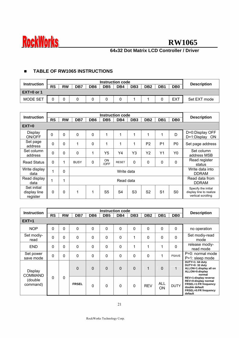
RW1065 64x32 Dot Matrix LCD Controller Driver
RockWorks Technology Corp
21
TABLE OF RW1065 INSTRUCTIONS
Instruction code Instruction RS RW DB7 DB6 DB5 DB4 DB3 DB2 DB1 DB0 Description
EXT=0 or 1
MODE SET 0 0 0 0 0 0 1 1 0 EXT Set EXT mode
Instruction code Instruction RS RW DB7 DB6 DB5 DB4 DB3 DB2 DB1 DB0 Description
EXT=0 Display ONOFF 0 0 0 0 1 1 1 1 1 D D=0Display OFF
D=1Display ONSet page address 0 0 1 0 1 1 1 P2 P1 P0 Set page address
Set column address 0 0 0 1 Y5 Y4 Y3 Y2 Y1 Y0 Set column
address MSB
Read Status 0 1 BUSY 0 ON OFF RESET 0 0 0 0 Read register
status Write display
data 1 0 Write data Write data into DDRAM
Read display data 1 1 Read data Read data from
DDRAM Set initial
display line register
0 0 1 1 S5 S4 S3 S2 S1 S0 Specify the initial
display line to realize vertical scrolling
Instruction code Instruction RS RW DB7 DB6 DB5 DB4 DB3 DB2 DB1 DB0 Description
EXT=1
NOP 0 0 0 0 0 0 0 0 0 0 no operation
Set modiy-read 0 0 0 0 0 0 1 0 0 0 Set modiy-read
mode
END 0 0 0 0 0 0 1 1 1 0 release modiy-read mode
Set power save mode 0 0 0 0 0 0 0 0 1 PSAVE P=0 normal mode
P=1 sleep mode
0 0 0 0 0 1 0 1 Display
COMMAND (double
command)
0 0 FRSEL
0 0 0 0 REV ALLON DUTY
DUTY=1 64 duty DUTY=0 32 duty ALLON=1display all on ALLON=0display
normal REV=1display reverse REV=0display normal FRSEL=1FR frequency double default FRSEL=0FR frequency default
RW1065 64x32 Dot Matrix LCD Controller Driver
RockWorks Technology Corp
22
Command Description
See the Table of RW1065 instructions The RW1065 series identifies a data bus using a combination of RS E and RW signals As the MPU translates a command in the internal timing only (independent from the external clock) its speed is very high The busy check is usually not required
Display ONOFF
EXT RS RW D7 D6 D5 D4 D3 D2 D1 D0
0 0 0 0 0 1 1 1 1 1 D
This command turns the display on and off D=1 Display ON D=0 Display OFF(default)
Set page Address This command specifies the page address that corresponds to the low address of the display data RAM when it is accessed by the MPU Any bit of the display data RAM can be accessed when its page address and column address are specified The display status is not changed even when the page address is changed
EXT RS RW D7 D6 D5 D4 D3 D2 D1 D0
0 0 0 1 0 1 1 1 A2 A1 A0
This command loads the page address register
A2 A1 A0 Page
0 0 0 0 (default)
0 0 1 1 0 1 0 2 0 1 1 3 1 0 0 4 1 0 1 5 1 1 0 6 1 1 1 7
Page mapping see Figure 4
RW1065 64x32 Dot Matrix LCD Controller Driver
RockWorks Technology Corp
23
Set Column Address This command specifies a column address of the display data RAM When the display data RAM is accessed by the MPU continuously the column address is incremented by I each time it is accessed from the set address Therefore the MPU can access to data continuously The column address stops to be incremented at address 63 and the page address is not changed continuously
EXT RS RW D7 D6 D5 D4 D3 D2 D1 D0
0 0 0 0 1 A5 A4 A3 A2 A1 A0
A5 A4 A3 A2 A1 A0 Column Address0 0 0 0 0 0 0(default) 0 0 0 0 0 1 1
1 1 1 1 1 1 63
Read Status
EXT RS RW D7 D6 D5 D4 D3 D2 D1 D0
0 0 1 BUSY 0 ON OFF RESET 0 0 0 0
The BUSY Flag bit indicates that RW 1065 is operating or no operating
BUSY=1 Operation BUSY=0 Ready
The ONOFF bit indicates the current status of the display It is the inverse of the polarity of the display ONOFF command ONOFF=1 Display OFF ONOFF=0 Display ON The RESET bit indicates whether the driver is executing a hardware or software reset or if it is in normal operating mode RESET=1 Currently executing reset command RESET=0 Normal operation
RW1065 64x32 Dot Matrix LCD Controller Driver
RockWorks Technology Corp
24
Write Display Data
EXT RS RW D7 D6 D5 D4 D3 D2 D1 D0
0 1 0 Write data
Writes 8-bits of data into the display data RAM at a location specified by the contents of the column address and page address registers and then increments the column address register by one
Read Display Data
EXT RS RW D7 D6 D5 D4 D3 D2 D1 D0
0 1 1 Read data
Reads 8-bits of data from the data IO latch updates the contents of the IO latch with display data from the display data RAM location specified by the contents of the column address and page address registers and then increments the column address register After loading a new address into the column address register one dummy read is required before valid data is obtained
Set initial display line register
EXT RS RW D7 D6 D5 D4 D3 D2 D1 D0
0 0 0 1 1 S5 S4 S3 S2 S1 S0
Loads the RAM line address of the initial display line COM 0 into the initial display line register The RAM display data becomes the top line of the LCD screen It is followed by the higher number lines in ascending order corresponding to the duty cycle The screen can be scrolled using this command by incrementing the line address(default value=rdquo00Hrdquo)
RW1065 64x32 Dot Matrix LCD Controller Driver
RockWorks Technology Corp
25
Read-Modify-Write
EXT RS RW D7 D6 D5 D4 D3 D2 D1 D0
1 0 0 0 0 0 0 1 0 0 0
This command defeats column address register auto-increment after data reads The current contents of the column Address register are saved The mode remains active until an End command is received When the End command is entered the column address is returned to the one used during input of Read-Modify-Write Command This function can reduce the load of MPU when data change is repeated as a specific display area Any command other than Data Read or Write can be used in the Read-Modify-Write mode However the Column Address Set command cannot be used
End
EXT RS RW D7 D6 D5 D4 D3 D2 D1 D0
1 0 0 0 0 0 0 1 1 1 0
This command cancels read-modify-write mode and restores the contents of the column address register to their value prior to the receipt of the Read-Modify-Write command
N N+1 N+2 N+3 N+m N
Read -modify-write mode set End
Returm
Column address
Set page address
Set column address
Read-modify-write
Dummy read
Read data
Write data
End
CompletedNo
Yes
RW1065 64x32 Dot Matrix LCD Controller Driver
RockWorks Technology Corp
26
Set power save mode
EXT RS RW D7 D6 D5 D4 D3 D2 D1 D0
1 0 0 0 0 0 0 0 0 1 PSAVE
When power save mode is entered thus greatly reducing power consumption In the power save mode the display data is saved as is the operating mode that was in effect before the power saver mode was initiated and the MPU is still able to access the display data RAM PSAVE=1 Sleep mode PSAVE=0 Normal mode Sleep mode This stops all operations in the LCD display system and as long as there are no accesses from the MPU the consumption current is reduced to a value near the static current The internal modes during sleep mode are as follows 1 The oscillator circuit and the LCD power supply circuit are halted 2 All liquid crystal drive circuits are halted and the segment and common drive outputs output a Vss level
Display command double command
EXT RS RW D7 D6 D5 D4 D3 D2 D1 D0
1 0 0 0 0 0 0 0 1 0 1
1 0 0 FRSEL 0 0 0 0 REV ALLON DUTY
Display NormalReverse set REV=1 Reverse REV=0 Normal(default) Display All Point ONOFF ALLON=1 All display points ON ALLON=0 Normal(default) Select Duty Duty=1 164 duty cycle(default) Duty=0 132 duty cycle FRAME FREQUENCY Select FRSEL=1 Double FRSEL=0 (default)
RW1065 64x32 Dot Matrix LCD Controller Driver
RockWorks Technology Corp
27
Hardware Pin Set
Select ADC by ADC Pin The pin selects the relationship between display data RAM column addresses and segment drivers ADC=1 SEG0larrcolumn address 3FHhellipinverted ADC=0 SEG0larrcolumn address 00Hhellipnormal(default) This command is provided to reduce restrictions on the placement of driver ICs and routing of traces during printed circuit Board design See Figure 4 for a table of segments and column addresses for the two values of D
Select SHL by SHL Pin The pin selects the com output scan direction SHL=1 Reverse directioncom63rarrcom0 SHL=0 Normal com0rarrcom63 Both master and slave should set identical SHL value
Select LCD Bias by BS0 BS1 Pin
BS1 BS0 Bias 0 0 15 bias 0 1 16 bias 1 0 18 bias 1 1 19 bias
RW1065 64x32 Dot Matrix LCD Controller Driver
RockWorks Technology Corp
28
When an External Resistance is Used The liquid crystal power supply voltage V0 is set by adding resistors Rarsquo and Rbrsquo between VDD and VR and between VR and V0 respectively
RW1065
RW1065 64x32 Dot Matrix LCD Controller Driver
RockWorks Technology Corp
29
The set voltage circuits
Using the step-up voltage circuits equipped within the RW1065 chips it is possible to produce a 2X 3X 4X step-up voltage levels 2X step-up
To produce voltage level in the positive direction at the Vout terminal that is 2 times the voltage difference between VSS and VDD2 Please configure set voltage circuits like this Place a 1uF~22uF capacitor between CAP1N and CAP1P Place a 1uF~22uF capacitor between VSS and VOUT Short CAP2P CAP3P and VOUT Leave CAP2N open 3X step-up
To produce voltage level in the positive direction at the Vout terminal that is 3 times the voltage difference between VSS and VDD2 Please configure set voltage circuits like this Place a 1uF~22uF capacitor between CAP1N and CAP1P Place a 1uF~22uF capacitor between VSS and VOUT Place a 1uF~22uF capacitor and 100 ohms resistor between CAP2N and CAP2P Short CAP3P and Vout 4X step-up
To produce voltage level in the positive direction at the Vout terminal that is 4 times the voltage difference between VSS and VDD2 Please configure set voltage circuits like this Place a 1uF~22uF capacitor between CAP1N and CAP1P Place a 1uF~22uF capacitor between VSS and VOUT Place a 1uF~22uF capacitor and 100 ohms resistor between CAP2N and CAP2P Place a 1uF~22uF capacitor and 100 ohms resistor between CAP1N and CAP3P
RW1065 64x32 Dot Matrix LCD Controller Driver
RockWorks Technology Corp
30
ABSOLUTE MAXIMUM RATINGS Characteristics Symbol Value Unit
Power supply voltage VDD -03 to +70 V
LCD driver voltage Vout 0 to +17 V
Input voltage VIN -03 to VDD+03 V
Operating temperature TA -40 to +85
Storage temperature TSTO -55 to +125
DC CHARACTERISTICS
Rating Item Symbol Condition Min Typ Max Unit ApplicablePin
Operating Voltage VDD - 27 30 55 V VDD1
Step up output voltage Vout (Relative to VDD) 0 - 17 V Vout
Voltage follower circuit operating Voltage V0 (Relative to VDD) 0 - 15 V V0
V0 accuracy V0 - 0 - 15 V0
High-level Input Voltage Low-level Input Voltage
VIHC VILC - 07 VDD
Vss - VDD 09 V 2
High-level Output Voltage Low-level Output Voltage
VOHC VOLC
IOH = ndash05 mA IOL = 05 mA
08VDD Vss - VDD
02 VDD V 3
Input leakage current ILI VIN = VDD or VSS -1 - 2 uA 4
Output leakage current ILO - -1 1 uA 5
Liquid Crystal Driver ON Resistance RON
Ta= 25degC(Relative To VDD)
V0 =15 V - 16 20 KΩ SEGn COMn 6
Internal Oscillator fOSC 2286 254 2794 Oscillator
Frequency External Input RECOMMAND fCL
Ta = 25degC 132Duty 2286 254 2794
kHz CL
Internal Oscillator fOSC 45 5 55 Oscillator
Frequency External Input RECOMMAND fCL
Ta = 25degC 164Duty 45 5 55
kHz CL
bullDynamic Consumption Current During Display with the Internal Power Supply OFF Current consumed by total ICs when an external power supply is used
Unless otherwise specified Vss=0V VDD=30V
RW1065 64x32 Dot Matrix LCD Controller Driver
RockWorks Technology Corp
31
Display Pattern OFF
Ta = 25degC Vout=17V Rating Item Symbol Condition Min Typ Max Unit Notes
VDD=30 V V0-Vss=8V - 10 15 RW1065 IDD VDD=50 V V0-Vss=8V - 35 45
microA 7
Display Pattern Checker
Ta = 25degC Vout=17V Rating Item Symbol Condition Min Typ Max Unit Notes
VDD=30 V V0-Vss=8V - 15 20 RW1065 IDD VDD=50 V V0-Vss=8V - 40 50
microA 7
Display Pattern OFF
Ta = 25degC Vout=17V Rating Item Symbol Condition Min Typ Max Unit Notes
VDD=30 V V0-Vss=8V - 15 20 RW1065 IDD VDD=50 V V0-Vss=8V - 40 50
microA 7
Display pattern Checker
Ta = 25degC Vout=17V Rating Item Symbol Condition Min Typ Max Unit Notes
VDD=30 V V0-Vss=8V - 65 80 RW1065 IDD VDD=50 V V0-Vss=8V - 130 150
microA 7
bull Consumption Current at Time of Power Saver Mode VSS = 0 V VDD = 30 V plusmn 10
Rating Item Symbol Condition Min Typ Max Unit Notes
Sleep mode IDD - - 5 10 microA -
References for items market with 1 While a broad range of operating voltages is guaranteed performance cannot be guaranteed if there are sudden fluctuations to the
voltage while the MPU is being accessed 2 The RS D0 to D5 D6 D7 E RW CS1BP CS2P CLS CL FR MS and RST
― terminals
3 The D0 to D7 FR and CL terminals 4 The RS E RW CS1BP CS2P CLS MS and RST
― terminals
5 Applies when the D0 to D5 D6 D7 CL and FR terminals are in a high impedance state 6 These are the resistance values for when a 01 V voltage is applied between the output terminals SEGn or COMn and
the various power supply terminals (V1 V2 V3 and V4) These are specified for the operating voltage (3) range RON = 01 V ∆I (Where ∆I is the current that flows when 01 V is applied while the power supply is ON)
7 It indicates the current consumed on ICs alone when the internal oscillator circuit and display are turned on Does not include the current due to the LCD panel capacity and wiring capacity Applicable only when there is no access from the MPU
RW1065 64x32 Dot Matrix LCD Controller Driver
RockWorks Technology Corp
32
TIMING CHARACTERISTICS
68 Interface
(Ta=-40 to 85 degC) VDD=27 to 45V
Rating VDD=45 to 55V
Rating Item Signal Symbol ConditionMin Max Min Max
Units
Address hold time RS tAH6 0 mdash 0 mdash Address setup time RS tAW6
mdash 0 mdash 0 mdash
ns
System cycle time RS tCYC6 mdash 900 mdash 800 mdash ns Data setup time D0 to D7 tDS6 100 mdash 100 mdash Data hold time D0 to D7 tDH6
mdash 0 mdash 0 mdash
ns
Access time D0 to D7 tACC6 mdash 350 mdash 250
Output disable time D0 to D7 tOH6 CL = 100 pF
mdash 300 mdash 200 ns
Read tEWHR 360 mdash 300 mdash Enable H pulse time
WriteE
tEWHW mdash
360 mdash 300 mdash ns
Read tEWLR 450 mdash 400 mdash Enable L pulse time
WriteE
tEWLW mdash
450 mdash 400 mdash ns
1 All timing is specified using 20 and 80 of VDD as the reference 2 tEWLW and tEWLR are specified as the overlap between CS1BP being ldquoLrdquo (CS2P = ldquoHrdquo) and E
RW1065 64x32 Dot Matrix LCD Controller Driver
RockWorks Technology Corp
33
Reset Timing
Rating Item Signal Symbol Condition
Min Typ Max Units
Reset time mdash tR mdash mdash - 2 micros
Reset ldquoLrdquo pulse width RST tRW mdash 2 - mdash micros
1 When double chip was be used then the duty set command must be set between the tR
RW1065 64x32 Dot Matrix LCD Controller Driver
RockWorks Technology Corp
34
IO PAD CONFIGURATION
RW1065 64x32 Dot Matrix LCD Controller Driver
RockWorks Technology Corp
35
THE MPU INTERFACE (REFERENCE EXAMPLES) The RW1065 Series can be connected to 6800 Series MPUs The display area can be enlarged by using multiple RW1065 Series chips When this is done the chip select signal can be used to select the individual ICs to access
6800 Series MPUs
RW
106
5
RW1065 64x32 Dot Matrix LCD Controller Driver
RockWorks Technology Corp
36
When using external multi-level power supply for LCD driving (REFERENCE EXAMPLE)
Using a resistor divider can provide RW1065 external multi-level power supply for LCD driving
The circuit below shows a resistor divider network which can bias V0 V1 V2 V3 and V4 externally
RW1065 64x32 Dot Matrix LCD Controller Driver
RockWorks Technology Corp
37
bullWhen V0 V1 V2 V3 and V4 are biased by external power supply analog section of RW1065 should be turn off by software during LCD initialization The example in below shows the sequence to turn off analog section when external bias is used Begin of LCD initialization 1 Reset RW1065 2 SET EXT=1 (mode instruction)
RS RW DB7 DB6 DB5 DB4 DB3 DB2 DB1 DB00 0 0 0 0 0 1 1 0 1
3 SET Display Command (double command)
RS RW DB7 DB6 DB5 DB4 DB3 DB2 DB1 DB00 0 0 0 0 0 0 1 0 1 0 0 0 0 1 1 0 0 0 1
4 SET EXT=1 (mode instruction)
RS RW DB7 DB6 DB5 DB4 DB3 DB2 DB1 DB00 0 0 0 0 0 1 1 0 0
End of LCD initialization
bullBecause pins can not set LCD bias when external power supplies are used for LCD driving the bias can be set by an appropriate configuration for a resistor voltage divider networks The example is shown below
VSS
R
R
NR
R
R
RV1
RV2
RV3
RV4
V0
Bias Network Circuit Concept 15 Bias N=1 total = 5R 16 Bias N=2 total =6R 18 Bias N=4 total =8R 19 Bias N=5 total = 9R
RW1065 64x32 Dot Matrix LCD Controller Driver
RockWorks Technology Corp
38
Single chip solution for RW1065 application (REFERENCE EXAMPLE)
For a 64x32 application the duty cycle of LCD panel is 164 and the display duty of RW1065 should be set to 164 The display duty cycle can be selected by the DUTY bit in display command The diagram for 64x32 application is shown below
64 SEGx32COM LCD Panel
164 duty cycle
RW1065 DUTY=1
COM1~33
SEG1~65
RW1065 64x32 Dot Matrix LCD Controller Driver
RockWorks Technology Corp
39
Using an adjustable resistor on the main board to adjust the contrast of liquid crystal display (REFERENCE EXAMPLE)
The schematic shows an adjustable resistor on main board that can adjust voltage level of V0
RW1065 64x32 Dot Matrix LCD Controller Driver
RockWorks Technology Corp
40
Package information (Please pay close attention to the information in this section Do not hesitate to consult with our sale representative if you have any question or concern)
In order to make better bonding yield for RW1065 please follow the tips and recommendations in this section In this section few tips about COB footprint style PCB layout and wire bonding will be discussed
The drawing in below shows the PCB footprint style which we recommend for RW1065 Pads array in
curve shape is easier for Al wire bonding Besides that a real size COB footprint for RW1065 is also shown in below RW1065 COB footprint is also available in powerpcb or protel format for design reference purpose
The ratio is 11
RW1065 64x32 Dot Matrix LCD Controller Driver
RockWorks Technology Corp
41
During COB footprint design there have some tips about footprint that the PCB designer should know The angle between bonding wire and vertical line should less than 45 Otherwise the wire shorts would become very easy to happen at fours corners of the chip
The angle between bonding wire and vertical line could be reduced by expanding the distance between pads array and the chip In addition reducing length in horizon direction of pads array could minimize the angle between bonding wire and vertical line The picture in below will help to illustrate this concept From the experiences COB footprint style affects the bonding yield
Bad Wires are too close to each other
The angle between bonding wire and vertical line is greater than 45
The angle between bonding wire and vertical line is less than 45
Wires are not too close to each other
Reducing length in horizon direction of pads array could minimize the angle between bonding wire and vertical line
The angle between bonding wire and vertical line could be reduced by expanding the distance between pads array and the chip
RW1065 64x32 Dot Matrix LCD Controller Driver
RockWorks Technology Corp
42
If the gap between pads of COB footprint is filled with solder mask coating it is difficult to bond Al wire to
the pads The top solder masks layer that overlap COB footprint area should be removed
Please use 1 mils diameter Al wire for RW1065 wire bonding
1 2 3 4 5 6
A
B
C
D
654321
D
C
B
A
Title
Number RevisionSize
C
Date 29-Aug-2007 Sheet of File D公司資料99seMyDesignddb Drawn By
RW1065
COM131
COM142
COM153
COM164
COM175
COM186
COM197
COM208
COM219
COM2210
COM2311
COM2412
COM2513
COM2614
COM2715
COM2816
COM2917
COM3018
COM3119
SEG
6320
SEG
6221
SEG
6122
SEG
6023
SEG
5924
SEG
5825
SEG
5726
SEG
5627
SEG
5528
SEG
5429
SEG
5330
SEG
5231
SEG
5132
SEG
5033
SEG
4934
SEG
4835
SEG
4736
SEG
4637
SEG
4538
SEG
4439
SEG
4340
SEG
4241
SEG
4142
SEG
4043
SEG
3944
SEG
3845
SEG
3746
SEG
3647
SEG
3548
SEG
3449
SEG
3350
SEG
3251
SEG
3152
SEG
3053
SEG
2954
SEG
2855
SEG
2756
SEG
2657
SEG
2558
SEG
2459
SEG
2360
SEG
2261
SEG
2162
SEG
2063
SEG
1964
SEG
1865
SEG
1766
SEG
1667
SEG
1568
SEG
1469
SEG13 70SEG12 71SEG11 72SEG10 73SEG9 74SEG8 75SEG7 76SEG6 77SEG5 78SEG4 79SEG3 80SEG2 81SEG1 82SEG0 83ADCP 84CLL 85
VSS
86D
087
D1
88D
289
D3
90D
491
D5
92D
693
D7
94C
S1B
P95
CS2
P96
ERD
P97
AO
P(R
S)98
RW
RP
99V
DD
100
RST
P10
1C
LSP
102
FRR
103
MSP
104
BS1
P10
5B
S0P
106
SHLP
107
VD
D2
108
CA
P2N
109
CA
P2P
110
CA
P1P
111
CA
P1N
112
CA
P3P
113
VO
UT
114
V0
115
VR
AB
116
V3
117
V2
118
V4
119
V1
120
CO
M0
121
CO
M1
122
CO
M2
123
CO
M3
124
CO
M4
125
CO
M5
126
CO
M6
127
CO
M7
128
CO
M8
129
CO
M9
130
CO
M10
131
CO
M11
132
CO
M12
133
4897x1902 um
IC1
RW1065
C9CAPR4
100R0603
R30R0603
C8
CAP
C7
CAP
R2
100R0603
R1
0R0603C6 22uf
R50R
R6300R
R7RES1
R8NC R9
100R0603
VDD
R10
NC
R11
100R0603
R12
100R0603
R13
NC
R14
100R0603
R15
NC
VDD
D0
D1
D2
D3
D4
D5
D6
D7
DB[07]
VDDC5
01uf0603
VD
D
CS2
P
123456789
1011121314151617181920
J1
CON20
C1201uf0603
R3951K0603
VDD
CAP Value1UF~22UF
2XPut C6C8 Short R1R3Open R2R4C7C93XPut C6C8C9 R4Short R1Open R2R3C74XOpen R1R3
BS0 BS1 Bias0 0
0 1
1 0
11
15 bias
16 bias
18 bias
19 bias
ADC=0 SEG0lt~column address 00Hnormal(default) ADC=1 SEG0lt~column address 3FHinverted
SHL=0 Normal COM0~gtCOM63(default)SHL=1 Reverse direction COM63~gtCOM0
R16100R0603
LCD PANEL 64X32RockWorks
RW1065 64X32
COM0-31 SEG0-63SHL=0 ADC=0
SHL=1COM31-0
ADC=1SEG63-0
if use single chip for 32 command displaythe display command must select 164 dutyDisplay panel must select 164 duty type
VO
UT
C3P
C1N
C1P
C2P
C2N
VDD2
ADC
SHL
BS0
BS1
CLLADC
V1
V2
V3
V4
VR
AB
V0
VO
UT
C3P
C1N
C1P
C2P
C2N
VD
D2
SHL
BS0
BS1
FRR
RST
P
RW
RS
E CS1
B
CS1
V0RSRWED0D1D2D3D4D5D6D7
RSTPAK
C4
22uf
RBRES1
RA1RES1
C2
22uf
C1
22uf
C3
22uf
C0
22uf
R20
100k0603
R21
100k0603
R17
200K0603
V1
V2
V3
V4 VRAB
V0
V0
OPTION
B
R18
300R0603
RA2RES1
VADJ
R19100R
R23 RES1R22 0R
R24
RES1
R25
0R
VDD
CS1BP
CS2P
CS1
CS1
R26
22R0603
R27
22R0603
C1047uf
C11
01uf
VSS_INVDD_IN
D1DIODE
FGND
鐵框地
VSS
VDD
R28 10RR29 10RR30 10RR31 10RR32 10RR33 10RR34 10RR35 10RR36 10RR37 10RR38 10R
VADJ
1 2 3 4 5 6
A
B
C
D
654321
D
C
B
A
Title
Number RevisionSize
C
Date 29-Aug-2007 Sheet of File D公司資料99seMyDesignddb Drawn By
RW1065
COM131
COM142
COM153
COM164
COM175
COM186
COM197
COM208
COM219
COM2210
COM2311
COM2412
COM2513
COM2614
COM2715
COM2816
COM2917
COM3018
COM3119
SEG
6320
SEG
6221
SEG
6122
SEG
6023
SEG
5924
SEG
5825
SEG
5726
SEG
5627
SEG
5528
SEG
5429
SEG
5330
SEG
5231
SEG
5132
SEG
5033
SEG
4934
SEG
4835
SEG
4736
SEG
4637
SEG
4538
SEG
4439
SEG
4340
SEG
4241
SEG
4142
SEG
4043
SEG
3944
SEG
3845
SEG
3746
SEG
3647
SEG
3548
SEG
3449
SEG
3350
SEG
3251
SEG
3152
SEG
3053
SEG
2954
SEG
2855
SEG
2756
SEG
2657
SEG
2558
SEG
2459
SEG
2360
SEG
2261
SEG
2162
SEG
2063
SEG
1964
SEG
1865
SEG
1766
SEG
1667
SEG
1568
SEG
1469
SEG13 70SEG12 71SEG11 72SEG10 73SEG9 74SEG8 75SEG7 76SEG6 77SEG5 78SEG4 79SEG3 80SEG2 81SEG1 82SEG0 83ADCP 84CLL 85
VSS
86D
087
D1
88D
289
D3
90D
491
D5
92D
693
D7
94C
S1B
P95
CS2
P96
ERD
P97
AO
P(R
S)98
RW
RP
99V
DD
100
RST
P10
1C
LSP
102
FRR
103
MSP
104
BS1
P10
5B
S0P
106
SHLP
107
VD
D2
108
CA
P2N
109
CA
P2P
110
CA
P1P
111
CA
P1N
112
CA
P3P
113
VO
UT
114
V0
115
VR
AB
116
V3
117
V2
118
V4
119
V1
120
CO
M0
121
CO
M1
122
CO
M2
123
CO
M3
124
CO
M4
125
CO
M5
126
CO
M6
127
CO
M7
128
CO
M8
129
CO
M9
130
CO
M10
131
CO
M11
132
CO
M12
133
4897x1902 um
IC1
RW1065 Master
RW1065
COM131
COM142
COM153
COM164
COM175
COM186
COM197
COM208
COM219
COM2210
COM2311
COM2412
COM2513
COM2614
COM2715
COM2816
COM2917
COM3018
COM3119
SEG
6320
SEG
6221
SEG
6122
SEG
6023
SEG
5924
SEG
5825
SEG
5726
SEG
5627
SEG
5528
SEG
5429
SEG
5330
SEG
5231
SEG
5132
SEG
5033
SEG
4934
SEG
4835
SEG
4736
SEG
4637
SEG
4538
SEG
4439
SEG
4340
SEG
4241
SEG
4142
SEG
4043
SEG
3944
SEG
3845
SEG
3746
SEG
3647
SEG
3548
SEG
3449
SEG
3350
SEG
3251
SEG
3152
SEG
3053
SEG
2954
SEG
2855
SEG
2756
SEG
2657
SEG
2558
SEG
2459
SEG
2360
SEG
2261
SEG
2162
SEG
2063
SEG
1964
SEG
1865
SEG
1766
SEG
1667
SEG
1568
SEG
1469
SEG13 70SEG12 71SEG11 72SEG10 73SEG9 74SEG8 75SEG7 76SEG6 77SEG5 78SEG4 79SEG3 80SEG2 81SEG1 82SEG0 83ADCP 84CLL 85
VSS
86D
087
D1
88D
289
D3
90D
491
D5
92D
693
D7
94C
S1B
P95
CS2
P96
ERD
P97
AO
P(R
S)98
RW
RP
99V
DD
100
RST
P10
1C
LSP
102
FRR
103
MSP
104
BS1
P10
5B
S0P
106
SHLP
107
VD
D2
108
CA
P2N
109
CA
P2P
110
CA
P1P
111
CA
P1N
112
CA
P3P
113
VO
UT
114
V0
115
VR
AB
116
V3
117
V2
118
V4
119
V1
120
CO
M0
121
CO
M1
122
CO
M2
123
CO
M3
124
CO
M4
125
CO
M5
126
CO
M6
127
CO
M7
128
CO
M8
129
CO
M9
130
CO
M10
131
CO
M11
132
CO
M12
133
4897x1902 um
IC2
RW1065 Slave
C4
22uf
RBRES1
RA1RES1
C2
22uf
C1
22uf
C3
22uf
C0
22ufC9CAPR4
100R0603
R30R0603
C8
CAP
C7
CAP
R2
100R0603
R1
0R0603C6 22uf
R50R0603
R6300R0603
R7RES1
R8NC R9
100R0603
VDD
R10
NC
R11
100R0603
R12
NC
R13
100R0603
R14
100R0603
R15
NC
R16
100R0603
R17
NC
VDD
D0
D1
D2
D3
D4
D5
D6
D7
D0
D1
D2
D3
D4
D5
D6
D7
DB[07] DB[07]
VDDC10
01uf0603
VD
D
IC1_
CS2
P
VDD
IC2_
CS2
P
VD
D
C11
01uf0603
VSS
VSS
LCD PANEL 128X64
Master COM0-31 Slave COM32-63
Master SEG0-63 Slave SEG64-127
123456789
1011121314151617181920
J1
CON20
Master Slave
CAP Value1UF~22UF
2XPut C6C8 Short R1R3Open R2R4C7C93XPut C6C8C9 R4Short R1Open R2R3C74XOpen R1R3
RockWorksRW1065 128x64
BS0 BS1 Bias0 0
0 1
1 0
11
15 bias
16 bias
18 bias
19 bias
ADC=0 SEG0lt~column address 00Hnormal(default) ADC=1 SEG0lt~column address 3FHinverted
SHL=0 Normal COM0~gtCOM63(default)SHL=1 Reverse direction COM63~gtCOM0Both Master and Slave should set identical SHL value
SHL=0 SHL=0
ADC=0 ADC=0
Slave COM31-0
Slave SEG127-64
SHL=1
ADC=1
SHL=1Master COM63-32
ADC=1Master SEG63-0
R18100R0603
R22
100k0603
R23
100k0603
C501uF0603
R4551K0603
VDD
R19
200K0603
ADC1
ADC2
SHL
BS0
BS1
VDD2
V1
V2
V3
V4 VRAB
V0
V0V
OU
T
C3P
C1N
C1P
C2P
C2N
V1
V2
V3
V4
VR
AB
V0
VO
UT
C3P
C1N
C1P
C2P
C2N
VD
D2
SHL
BS0
BS1
FRR
RST
P
RW
RS
E IC1_
CS1
BP
V1
V2
V3
V4
VR
AB
V0
VO
UT
VD
D2
SHL
BS0
BS1
FRR
RST
P
RW
RS
E IC2_
CS1
BP
CLLADC1
CLLADC2
RSTP
CS1CS2
V0RSRWED0D1D2D3D4D5D6D7
AK
OPTION
R20
300R0603
RA2RES1
VADJ
R21
100R
B
R25 RESR24 0R
R26 RES R27 0RVDD
IC1_CS1BP
IC1_CS2P
CS1
CS1
R28 0R R29 RES
R30 RES R31 0R
IC2_CS1BP
IC2_CS2P
CS2
CS2
R32
22R0603
R33
22R0603
C1001uf
C11
47uf
D1DIODE
FGND
鐵框地
VSS
VDD
R34 10RR35 10RR36 10RR37 10RR38 10RR39 10RR40 10RR41 10RR42 10RR43 10RR44 10R
VSS_INVDD_IN
VADJ
VDD
1 2 3 4 5 6 7 8
A
B
C
D
87654321
D
C
B
A
Title
Number RevisionSize
D
Date 29-Aug-2007 Sheet of File D公司資料 99seMyDesignddb Drawn By
C422uf
RBRES1
RA1RES1
C3
22uf
C2
22uf
C1
22uf
C0
22ufC9CAPR4
100R0603
R30R0603
C8
CAP
C7
CAP
R2
100R0603
R1
0R0603C6 22uf
R220R0603
R23300R0603
R24RES1
R39
NCR40
100 ohm0603
VDD
R41
NC
R42
100 ohm0603
R43
NC
R44
100 ohm0603
R45
NC
R46
100 ohm0603
R47
100 ohm0603
R48
NC
R49
100 ohm0603
R50
NC
VDDCAP Value1UF~22UF
2XPut C6C8 Short R1R3Open R2R4C7C93XPut C6C8C9 R4Short R1Open R2R3C74XOpen R1R3
BS0 BS1 Bias0 0
0 1
1 0
11
15 bias
16 bias
18 bias
19 bias
ADC=0 SEG0lt~column address 00Hnormal(default)
ADC=1 SEG0lt~column address 3FHinverted
SHL=0 Normal COM0~gtCOM63(default)SHL=1 Reverse direction COM63~gtCOM0Both Master and Slave should set identical SHL value
R7
100k0603
R8
100k0603
V1
V2
V3
V4
V0
VRAB
V0
R5
200K
VDD2
VO
UT
C3P
C1N
C1P
C2P
C2N
ADC1
ADC2
ADC3
SHL
BS0
BS1
CS1CS2CS3
V0RSRWED0D1D2D3D4D5D6D7
RSTP
R3851K0603
C5
01uF
VDD
OPTION
R6
300R0603R9100R
RA2RES1
VADJ
RW1065
COM131
COM142
COM153
COM164
COM175
COM186
COM197
COM208
COM219
COM2210
COM2311
COM2412
COM2513
COM2614
COM2715
COM2816
COM2917
COM3018
COM3119
SEG
6320
SEG
6221
SEG
6122
SEG
6023
SEG
5924
SEG
5825
SEG
5726
SEG
5627
SEG
5528
SEG
5429
SEG
5330
SEG
5231
SEG
5132
SEG
5033
SEG
4934
SEG
4835
SEG
4736
SEG
4637
SEG
4538
SEG
4439
SEG
4340
SEG
4241
SEG
4142
SEG
4043
SEG
3944
SEG
3845
SEG
3746
SEG
3647
SEG
3548
SEG
3449
SEG
3350
SEG
3251
SEG
3152
SEG
3053
SEG
2954
SEG
2855
SEG
2756
SEG
2657
SEG
2558
SEG
2459
SEG
2360
SEG
2261
SEG
2162
SEG
2063
SEG
1964
SEG
1865
SEG
1766
SEG
1667
SEG
1568
SEG
1469
SEG13 70SEG12 71SEG11 72SEG10 73SEG9 74SEG8 75SEG7 76SEG6 77SEG5 78SEG4 79SEG3 80SEG2 81SEG1 82SEG0 83ADCP 84CLL 85
VSS
86D
087
D1
88D
289
D3
90D
491
D5
92D
693
D7
94C
S1B
P95
CS2
P96
ERD
P97
AO
P(R
S)98
RW
RP
99V
DD
100
RST
P10
1C
LSP
102
FRR
103
MSP
104
BS1
P10
5B
S0P
106
SHLP
107
VD
D2
108
CA
P2N
109
CA
P2P
110
CA
P1P
111
CA
P1N
112
CA
P3P
113
VO
UT
114
V0
115
VR
AB
116
V3
117
V2
118
V4
119
V1
120
CO
M0
121
CO
M1
122
CO
M2
123
CO
M3
124
CO
M4
125
CO
M5
126
CO
M6
127
CO
M7
128
CO
M8
129
CO
M9
130
CO
M10
131
CO
M11
132
CO
M12
133
4897x1902 um
IC1
RW1065 Master
RW1065
COM131
COM142
COM153
COM164
COM175
COM186
COM197
COM208
COM219
COM2210
COM2311
COM2412
COM2513
COM2614
COM2715
COM2816
COM2917
COM3018
COM3119
SEG
6320
SEG
6221
SEG
6122
SEG
6023
SEG
5924
SEG
5825
SEG
5726
SEG
5627
SEG
5528
SEG
5429
SEG
5330
SEG
5231
SEG
5132
SEG
5033
SEG
4934
SEG
4835
SEG
4736
SEG
4637
SEG
4538
SEG
4439
SEG
4340
SEG
4241
SEG
4142
SEG
4043
SEG
3944
SEG
3845
SEG
3746
SEG
3647
SEG
3548
SEG
3449
SEG
3350
SEG
3251
SEG
3152
SEG
3053
SEG
2954
SEG
2855
SEG
2756
SEG
2657
SEG
2558
SEG
2459
SEG
2360
SEG
2261
SEG
2162
SEG
2063
SEG
1964
SEG
1865
SEG
1766
SEG
1667
SEG
1568
SEG
1469
SEG13 70SEG12 71SEG11 72SEG10 73SEG9 74SEG8 75SEG7 76SEG6 77SEG5 78SEG4 79SEG3 80SEG2 81SEG1 82SEG0 83ADCP 84CLL 85
VSS
86D
087
D1
88D
289
D3
90D
491
D5
92D
693
D7
94C
S1B
P95
CS2
P96
ERD
P97
AO
P(R
S)98
RW
RP
99V
DD
100
RST
P10
1C
LSP
102
FRR
103
MSP
104
BS1
P10
5B
S0P
106
SHLP
107
VD
D2
108
CA
P2N
109
CA
P2P
110
CA
P1P
111
CA
P1N
112
CA
P3P
113
VO
UT
114
V0
115
VR
AB
116
V3
117
V2
118
V4
119
V1
120
CO
M0
121
CO
M1
122
CO
M2
123
CO
M3
124
CO
M4
125
CO
M5
126
CO
M6
127
CO
M7
128
CO
M8
129
CO
M9
130
CO
M10
131
CO
M11
132
CO
M12
133
4897x1902 um
IC2
RW1065 Slave
D0
D1
D2
D3
D4
D5
D6
D7
D0
D1
D2
D3
D4
D5
D6
D7
DB[07] DB[07]
VDDC8
01uf0603
VD
D
VDD
VD
D
C9
01uf0603
VSS
VSS
LCD PANEL 192X64
Master COM0-31 Slave COM32-63
Master SEG0-63 Slave SEG64-127
Master Slave
RockWorksRW1065 192x64
RW1065
COM131
COM142
COM153
COM164
COM175
COM186
COM197
COM208
COM219
COM2210
COM2311
COM2412
COM2513
COM2614
COM2715
COM2816
COM2917
COM3018
COM3119
SEG
6320
SEG
6221
SEG
6122
SEG
6023
SEG
5924
SEG
5825
SEG
5726
SEG
5627
SEG
5528
SEG
5429
SEG
5330
SEG
5231
SEG
5132
SEG
5033
SEG
4934
SEG
4835
SEG
4736
SEG
4637
SEG
4538
SEG
4439
SEG
4340
SEG
4241
SEG
4142
SEG
4043
SEG
3944
SEG
3845
SEG
3746
SEG
3647
SEG
3548
SEG
3449
SEG
3350
SEG
3251
SEG
3152
SEG
3053
SEG
2954
SEG
2855
SEG
2756
SEG
2657
SEG
2558
SEG
2459
SEG
2360
SEG
2261
SEG
2162
SEG
2063
SEG
1964
SEG
1865
SEG
1766
SEG
1667
SEG
1568
SEG
1469
SEG13 70SEG12 71SEG11 72SEG10 73SEG9 74SEG8 75SEG7 76SEG6 77SEG5 78SEG4 79SEG3 80SEG2 81SEG1 82SEG0 83ADCP 84CLL 85
VSS
86D
087
D1
88D
289
D3
90D
491
D5
92D
693
D7
94C
S1B
P95
CS2
P96
ERD
P97
AO
P(R
S)98
RW
RP
99V
DD
100
RST
P10
1C
LSP
102
FRR
103
MSP
104
BS1
P10
5B
S0P
106
SHLP
107
VD
D2
108
CA
P2N
109
CA
P2P
110
CA
P1P
111
CA
P1N
112
CA
P3P
113
VO
UT
114
V0
115
VR
AB
116
V3
117
V2
118
V4
119
V1
120
CO
M0
121
CO
M1
122
CO
M2
123
CO
M3
124
CO
M4
125
CO
M5
126
CO
M6
127
CO
M7
128
CO
M8
129
CO
M9
130
CO
M10
131
CO
M11
132
CO
M12
133
4897x1902 um
IC3
RW1065 Slave
D0
D1
D2
D3
D4
D5
D6
D7
DB[07]
VSS
VSS
VDD
VD
D
C10
01uf0603
Slave SEG128-192
Slave
SHL=0 SHL=0
Master COM63-32SHL=1 SHL=1
Slave COM31-0ADC=0 ADC=0 ADC=0
ADC=1 ADC=1 ADC=1Master SEG63-0 Slave SEG127-64 Slave SEG192-128
R50100R0603
V1
V2
V3
V4
VR
AB
V0
VO
UT
C3P
C1N
C1P
C2P
C2N
VD
D2
SHL
BS0
BS1
FRR
RST
P
RW
RS
E V1
V2
V3
V4
VR
AB
V0
VO
UT
VD
D2
SHL
BS0
BS1
FRR
RST
P
RW
RS
E V1
V2
V3
V4
VR
AB
V0
VO
UT
VD
D2
SHL
BS0
BS1
FRR
RST
P
RW
RS
E
CLL CLL CLLADC1 ADC2 ADC3
R25 10RR26 10RR27 10RR28 10RR29 10RR30 10RR31 10RR32 10RR33 10RR34 10RR35 10R
R36
22R0603
D1DIODE
R3722R0603
C647uf
C701uf
VSS_INVDD_IN
VSS
VDD
VADJ
123456789
101112131415161718192021222324
J1
CON24
AK
FGND
鐵框地
IC1_
CS1
BP
IC1_
CS2
P
IC2_
CS2
PIC
2_C
S1B
P
IC3_
CS1
BP
IC3_
CS2
B
R10 0R R11 RES
R12 RES R13 0RVDD
IC1_CS2B
IC1_CS1BPCS1
CS1
R14 0R R15 RES
R16 RES R17 0RVDDIC2_CS2B
IC2_CS1BPCS2
CS2
R18 0R R19 RES
R20 RES R21 0RVDDIC3_CS2B
IC3_CS1BPCS3
CS3
B
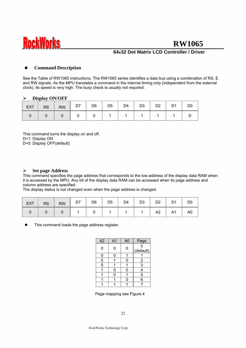
RW1065 64x32 Dot Matrix LCD Controller Driver
RockWorks Technology Corp
22
Command Description
See the Table of RW1065 instructions The RW1065 series identifies a data bus using a combination of RS E and RW signals As the MPU translates a command in the internal timing only (independent from the external clock) its speed is very high The busy check is usually not required
Display ONOFF
EXT RS RW D7 D6 D5 D4 D3 D2 D1 D0
0 0 0 0 0 1 1 1 1 1 D
This command turns the display on and off D=1 Display ON D=0 Display OFF(default)
Set page Address This command specifies the page address that corresponds to the low address of the display data RAM when it is accessed by the MPU Any bit of the display data RAM can be accessed when its page address and column address are specified The display status is not changed even when the page address is changed
EXT RS RW D7 D6 D5 D4 D3 D2 D1 D0
0 0 0 1 0 1 1 1 A2 A1 A0
This command loads the page address register
A2 A1 A0 Page
0 0 0 0 (default)
0 0 1 1 0 1 0 2 0 1 1 3 1 0 0 4 1 0 1 5 1 1 0 6 1 1 1 7
Page mapping see Figure 4
RW1065 64x32 Dot Matrix LCD Controller Driver
RockWorks Technology Corp
23
Set Column Address This command specifies a column address of the display data RAM When the display data RAM is accessed by the MPU continuously the column address is incremented by I each time it is accessed from the set address Therefore the MPU can access to data continuously The column address stops to be incremented at address 63 and the page address is not changed continuously
EXT RS RW D7 D6 D5 D4 D3 D2 D1 D0
0 0 0 0 1 A5 A4 A3 A2 A1 A0
A5 A4 A3 A2 A1 A0 Column Address0 0 0 0 0 0 0(default) 0 0 0 0 0 1 1
1 1 1 1 1 1 63
Read Status
EXT RS RW D7 D6 D5 D4 D3 D2 D1 D0
0 0 1 BUSY 0 ON OFF RESET 0 0 0 0
The BUSY Flag bit indicates that RW 1065 is operating or no operating
BUSY=1 Operation BUSY=0 Ready
The ONOFF bit indicates the current status of the display It is the inverse of the polarity of the display ONOFF command ONOFF=1 Display OFF ONOFF=0 Display ON The RESET bit indicates whether the driver is executing a hardware or software reset or if it is in normal operating mode RESET=1 Currently executing reset command RESET=0 Normal operation
RW1065 64x32 Dot Matrix LCD Controller Driver
RockWorks Technology Corp
24
Write Display Data
EXT RS RW D7 D6 D5 D4 D3 D2 D1 D0
0 1 0 Write data
Writes 8-bits of data into the display data RAM at a location specified by the contents of the column address and page address registers and then increments the column address register by one
Read Display Data
EXT RS RW D7 D6 D5 D4 D3 D2 D1 D0
0 1 1 Read data
Reads 8-bits of data from the data IO latch updates the contents of the IO latch with display data from the display data RAM location specified by the contents of the column address and page address registers and then increments the column address register After loading a new address into the column address register one dummy read is required before valid data is obtained
Set initial display line register
EXT RS RW D7 D6 D5 D4 D3 D2 D1 D0
0 0 0 1 1 S5 S4 S3 S2 S1 S0
Loads the RAM line address of the initial display line COM 0 into the initial display line register The RAM display data becomes the top line of the LCD screen It is followed by the higher number lines in ascending order corresponding to the duty cycle The screen can be scrolled using this command by incrementing the line address(default value=rdquo00Hrdquo)
RW1065 64x32 Dot Matrix LCD Controller Driver
RockWorks Technology Corp
25
Read-Modify-Write
EXT RS RW D7 D6 D5 D4 D3 D2 D1 D0
1 0 0 0 0 0 0 1 0 0 0
This command defeats column address register auto-increment after data reads The current contents of the column Address register are saved The mode remains active until an End command is received When the End command is entered the column address is returned to the one used during input of Read-Modify-Write Command This function can reduce the load of MPU when data change is repeated as a specific display area Any command other than Data Read or Write can be used in the Read-Modify-Write mode However the Column Address Set command cannot be used
End
EXT RS RW D7 D6 D5 D4 D3 D2 D1 D0
1 0 0 0 0 0 0 1 1 1 0
This command cancels read-modify-write mode and restores the contents of the column address register to their value prior to the receipt of the Read-Modify-Write command
N N+1 N+2 N+3 N+m N
Read -modify-write mode set End
Returm
Column address
Set page address
Set column address
Read-modify-write
Dummy read
Read data
Write data
End
CompletedNo
Yes
RW1065 64x32 Dot Matrix LCD Controller Driver
RockWorks Technology Corp
26
Set power save mode
EXT RS RW D7 D6 D5 D4 D3 D2 D1 D0
1 0 0 0 0 0 0 0 0 1 PSAVE
When power save mode is entered thus greatly reducing power consumption In the power save mode the display data is saved as is the operating mode that was in effect before the power saver mode was initiated and the MPU is still able to access the display data RAM PSAVE=1 Sleep mode PSAVE=0 Normal mode Sleep mode This stops all operations in the LCD display system and as long as there are no accesses from the MPU the consumption current is reduced to a value near the static current The internal modes during sleep mode are as follows 1 The oscillator circuit and the LCD power supply circuit are halted 2 All liquid crystal drive circuits are halted and the segment and common drive outputs output a Vss level
Display command double command
EXT RS RW D7 D6 D5 D4 D3 D2 D1 D0
1 0 0 0 0 0 0 0 1 0 1
1 0 0 FRSEL 0 0 0 0 REV ALLON DUTY
Display NormalReverse set REV=1 Reverse REV=0 Normal(default) Display All Point ONOFF ALLON=1 All display points ON ALLON=0 Normal(default) Select Duty Duty=1 164 duty cycle(default) Duty=0 132 duty cycle FRAME FREQUENCY Select FRSEL=1 Double FRSEL=0 (default)
RW1065 64x32 Dot Matrix LCD Controller Driver
RockWorks Technology Corp
27
Hardware Pin Set
Select ADC by ADC Pin The pin selects the relationship between display data RAM column addresses and segment drivers ADC=1 SEG0larrcolumn address 3FHhellipinverted ADC=0 SEG0larrcolumn address 00Hhellipnormal(default) This command is provided to reduce restrictions on the placement of driver ICs and routing of traces during printed circuit Board design See Figure 4 for a table of segments and column addresses for the two values of D
Select SHL by SHL Pin The pin selects the com output scan direction SHL=1 Reverse directioncom63rarrcom0 SHL=0 Normal com0rarrcom63 Both master and slave should set identical SHL value
Select LCD Bias by BS0 BS1 Pin
BS1 BS0 Bias 0 0 15 bias 0 1 16 bias 1 0 18 bias 1 1 19 bias
RW1065 64x32 Dot Matrix LCD Controller Driver
RockWorks Technology Corp
28
When an External Resistance is Used The liquid crystal power supply voltage V0 is set by adding resistors Rarsquo and Rbrsquo between VDD and VR and between VR and V0 respectively
RW1065
RW1065 64x32 Dot Matrix LCD Controller Driver
RockWorks Technology Corp
29
The set voltage circuits
Using the step-up voltage circuits equipped within the RW1065 chips it is possible to produce a 2X 3X 4X step-up voltage levels 2X step-up
To produce voltage level in the positive direction at the Vout terminal that is 2 times the voltage difference between VSS and VDD2 Please configure set voltage circuits like this Place a 1uF~22uF capacitor between CAP1N and CAP1P Place a 1uF~22uF capacitor between VSS and VOUT Short CAP2P CAP3P and VOUT Leave CAP2N open 3X step-up
To produce voltage level in the positive direction at the Vout terminal that is 3 times the voltage difference between VSS and VDD2 Please configure set voltage circuits like this Place a 1uF~22uF capacitor between CAP1N and CAP1P Place a 1uF~22uF capacitor between VSS and VOUT Place a 1uF~22uF capacitor and 100 ohms resistor between CAP2N and CAP2P Short CAP3P and Vout 4X step-up
To produce voltage level in the positive direction at the Vout terminal that is 4 times the voltage difference between VSS and VDD2 Please configure set voltage circuits like this Place a 1uF~22uF capacitor between CAP1N and CAP1P Place a 1uF~22uF capacitor between VSS and VOUT Place a 1uF~22uF capacitor and 100 ohms resistor between CAP2N and CAP2P Place a 1uF~22uF capacitor and 100 ohms resistor between CAP1N and CAP3P
RW1065 64x32 Dot Matrix LCD Controller Driver
RockWorks Technology Corp
30
ABSOLUTE MAXIMUM RATINGS Characteristics Symbol Value Unit
Power supply voltage VDD -03 to +70 V
LCD driver voltage Vout 0 to +17 V
Input voltage VIN -03 to VDD+03 V
Operating temperature TA -40 to +85
Storage temperature TSTO -55 to +125
DC CHARACTERISTICS
Rating Item Symbol Condition Min Typ Max Unit ApplicablePin
Operating Voltage VDD - 27 30 55 V VDD1
Step up output voltage Vout (Relative to VDD) 0 - 17 V Vout
Voltage follower circuit operating Voltage V0 (Relative to VDD) 0 - 15 V V0
V0 accuracy V0 - 0 - 15 V0
High-level Input Voltage Low-level Input Voltage
VIHC VILC - 07 VDD
Vss - VDD 09 V 2
High-level Output Voltage Low-level Output Voltage
VOHC VOLC
IOH = ndash05 mA IOL = 05 mA
08VDD Vss - VDD
02 VDD V 3
Input leakage current ILI VIN = VDD or VSS -1 - 2 uA 4
Output leakage current ILO - -1 1 uA 5
Liquid Crystal Driver ON Resistance RON
Ta= 25degC(Relative To VDD)
V0 =15 V - 16 20 KΩ SEGn COMn 6
Internal Oscillator fOSC 2286 254 2794 Oscillator
Frequency External Input RECOMMAND fCL
Ta = 25degC 132Duty 2286 254 2794
kHz CL
Internal Oscillator fOSC 45 5 55 Oscillator
Frequency External Input RECOMMAND fCL
Ta = 25degC 164Duty 45 5 55
kHz CL
bullDynamic Consumption Current During Display with the Internal Power Supply OFF Current consumed by total ICs when an external power supply is used
Unless otherwise specified Vss=0V VDD=30V
RW1065 64x32 Dot Matrix LCD Controller Driver
RockWorks Technology Corp
31
Display Pattern OFF
Ta = 25degC Vout=17V Rating Item Symbol Condition Min Typ Max Unit Notes
VDD=30 V V0-Vss=8V - 10 15 RW1065 IDD VDD=50 V V0-Vss=8V - 35 45
microA 7
Display Pattern Checker
Ta = 25degC Vout=17V Rating Item Symbol Condition Min Typ Max Unit Notes
VDD=30 V V0-Vss=8V - 15 20 RW1065 IDD VDD=50 V V0-Vss=8V - 40 50
microA 7
Display Pattern OFF
Ta = 25degC Vout=17V Rating Item Symbol Condition Min Typ Max Unit Notes
VDD=30 V V0-Vss=8V - 15 20 RW1065 IDD VDD=50 V V0-Vss=8V - 40 50
microA 7
Display pattern Checker
Ta = 25degC Vout=17V Rating Item Symbol Condition Min Typ Max Unit Notes
VDD=30 V V0-Vss=8V - 65 80 RW1065 IDD VDD=50 V V0-Vss=8V - 130 150
microA 7
bull Consumption Current at Time of Power Saver Mode VSS = 0 V VDD = 30 V plusmn 10
Rating Item Symbol Condition Min Typ Max Unit Notes
Sleep mode IDD - - 5 10 microA -
References for items market with 1 While a broad range of operating voltages is guaranteed performance cannot be guaranteed if there are sudden fluctuations to the
voltage while the MPU is being accessed 2 The RS D0 to D5 D6 D7 E RW CS1BP CS2P CLS CL FR MS and RST
― terminals
3 The D0 to D7 FR and CL terminals 4 The RS E RW CS1BP CS2P CLS MS and RST
― terminals
5 Applies when the D0 to D5 D6 D7 CL and FR terminals are in a high impedance state 6 These are the resistance values for when a 01 V voltage is applied between the output terminals SEGn or COMn and
the various power supply terminals (V1 V2 V3 and V4) These are specified for the operating voltage (3) range RON = 01 V ∆I (Where ∆I is the current that flows when 01 V is applied while the power supply is ON)
7 It indicates the current consumed on ICs alone when the internal oscillator circuit and display are turned on Does not include the current due to the LCD panel capacity and wiring capacity Applicable only when there is no access from the MPU
RW1065 64x32 Dot Matrix LCD Controller Driver
RockWorks Technology Corp
32
TIMING CHARACTERISTICS
68 Interface
(Ta=-40 to 85 degC) VDD=27 to 45V
Rating VDD=45 to 55V
Rating Item Signal Symbol ConditionMin Max Min Max
Units
Address hold time RS tAH6 0 mdash 0 mdash Address setup time RS tAW6
mdash 0 mdash 0 mdash
ns
System cycle time RS tCYC6 mdash 900 mdash 800 mdash ns Data setup time D0 to D7 tDS6 100 mdash 100 mdash Data hold time D0 to D7 tDH6
mdash 0 mdash 0 mdash
ns
Access time D0 to D7 tACC6 mdash 350 mdash 250
Output disable time D0 to D7 tOH6 CL = 100 pF
mdash 300 mdash 200 ns
Read tEWHR 360 mdash 300 mdash Enable H pulse time
WriteE
tEWHW mdash
360 mdash 300 mdash ns
Read tEWLR 450 mdash 400 mdash Enable L pulse time
WriteE
tEWLW mdash
450 mdash 400 mdash ns
1 All timing is specified using 20 and 80 of VDD as the reference 2 tEWLW and tEWLR are specified as the overlap between CS1BP being ldquoLrdquo (CS2P = ldquoHrdquo) and E
RW1065 64x32 Dot Matrix LCD Controller Driver
RockWorks Technology Corp
33
Reset Timing
Rating Item Signal Symbol Condition
Min Typ Max Units
Reset time mdash tR mdash mdash - 2 micros
Reset ldquoLrdquo pulse width RST tRW mdash 2 - mdash micros
1 When double chip was be used then the duty set command must be set between the tR
RW1065 64x32 Dot Matrix LCD Controller Driver
RockWorks Technology Corp
34
IO PAD CONFIGURATION
RW1065 64x32 Dot Matrix LCD Controller Driver
RockWorks Technology Corp
35
THE MPU INTERFACE (REFERENCE EXAMPLES) The RW1065 Series can be connected to 6800 Series MPUs The display area can be enlarged by using multiple RW1065 Series chips When this is done the chip select signal can be used to select the individual ICs to access
6800 Series MPUs
RW
106
5
RW1065 64x32 Dot Matrix LCD Controller Driver
RockWorks Technology Corp
36
When using external multi-level power supply for LCD driving (REFERENCE EXAMPLE)
Using a resistor divider can provide RW1065 external multi-level power supply for LCD driving
The circuit below shows a resistor divider network which can bias V0 V1 V2 V3 and V4 externally
RW1065 64x32 Dot Matrix LCD Controller Driver
RockWorks Technology Corp
37
bullWhen V0 V1 V2 V3 and V4 are biased by external power supply analog section of RW1065 should be turn off by software during LCD initialization The example in below shows the sequence to turn off analog section when external bias is used Begin of LCD initialization 1 Reset RW1065 2 SET EXT=1 (mode instruction)
RS RW DB7 DB6 DB5 DB4 DB3 DB2 DB1 DB00 0 0 0 0 0 1 1 0 1
3 SET Display Command (double command)
RS RW DB7 DB6 DB5 DB4 DB3 DB2 DB1 DB00 0 0 0 0 0 0 1 0 1 0 0 0 0 1 1 0 0 0 1
4 SET EXT=1 (mode instruction)
RS RW DB7 DB6 DB5 DB4 DB3 DB2 DB1 DB00 0 0 0 0 0 1 1 0 0
End of LCD initialization
bullBecause pins can not set LCD bias when external power supplies are used for LCD driving the bias can be set by an appropriate configuration for a resistor voltage divider networks The example is shown below
VSS
R
R
NR
R
R
RV1
RV2
RV3
RV4
V0
Bias Network Circuit Concept 15 Bias N=1 total = 5R 16 Bias N=2 total =6R 18 Bias N=4 total =8R 19 Bias N=5 total = 9R
RW1065 64x32 Dot Matrix LCD Controller Driver
RockWorks Technology Corp
38
Single chip solution for RW1065 application (REFERENCE EXAMPLE)
For a 64x32 application the duty cycle of LCD panel is 164 and the display duty of RW1065 should be set to 164 The display duty cycle can be selected by the DUTY bit in display command The diagram for 64x32 application is shown below
64 SEGx32COM LCD Panel
164 duty cycle
RW1065 DUTY=1
COM1~33
SEG1~65
RW1065 64x32 Dot Matrix LCD Controller Driver
RockWorks Technology Corp
39
Using an adjustable resistor on the main board to adjust the contrast of liquid crystal display (REFERENCE EXAMPLE)
The schematic shows an adjustable resistor on main board that can adjust voltage level of V0
RW1065 64x32 Dot Matrix LCD Controller Driver
RockWorks Technology Corp
40
Package information (Please pay close attention to the information in this section Do not hesitate to consult with our sale representative if you have any question or concern)
In order to make better bonding yield for RW1065 please follow the tips and recommendations in this section In this section few tips about COB footprint style PCB layout and wire bonding will be discussed
The drawing in below shows the PCB footprint style which we recommend for RW1065 Pads array in
curve shape is easier for Al wire bonding Besides that a real size COB footprint for RW1065 is also shown in below RW1065 COB footprint is also available in powerpcb or protel format for design reference purpose
The ratio is 11
RW1065 64x32 Dot Matrix LCD Controller Driver
RockWorks Technology Corp
41
During COB footprint design there have some tips about footprint that the PCB designer should know The angle between bonding wire and vertical line should less than 45 Otherwise the wire shorts would become very easy to happen at fours corners of the chip
The angle between bonding wire and vertical line could be reduced by expanding the distance between pads array and the chip In addition reducing length in horizon direction of pads array could minimize the angle between bonding wire and vertical line The picture in below will help to illustrate this concept From the experiences COB footprint style affects the bonding yield
Bad Wires are too close to each other
The angle between bonding wire and vertical line is greater than 45
The angle between bonding wire and vertical line is less than 45
Wires are not too close to each other
Reducing length in horizon direction of pads array could minimize the angle between bonding wire and vertical line
The angle between bonding wire and vertical line could be reduced by expanding the distance between pads array and the chip
RW1065 64x32 Dot Matrix LCD Controller Driver
RockWorks Technology Corp
42
If the gap between pads of COB footprint is filled with solder mask coating it is difficult to bond Al wire to
the pads The top solder masks layer that overlap COB footprint area should be removed
Please use 1 mils diameter Al wire for RW1065 wire bonding
1 2 3 4 5 6
A
B
C
D
654321
D
C
B
A
Title
Number RevisionSize
C
Date 29-Aug-2007 Sheet of File D公司資料99seMyDesignddb Drawn By
RW1065
COM131
COM142
COM153
COM164
COM175
COM186
COM197
COM208
COM219
COM2210
COM2311
COM2412
COM2513
COM2614
COM2715
COM2816
COM2917
COM3018
COM3119
SEG
6320
SEG
6221
SEG
6122
SEG
6023
SEG
5924
SEG
5825
SEG
5726
SEG
5627
SEG
5528
SEG
5429
SEG
5330
SEG
5231
SEG
5132
SEG
5033
SEG
4934
SEG
4835
SEG
4736
SEG
4637
SEG
4538
SEG
4439
SEG
4340
SEG
4241
SEG
4142
SEG
4043
SEG
3944
SEG
3845
SEG
3746
SEG
3647
SEG
3548
SEG
3449
SEG
3350
SEG
3251
SEG
3152
SEG
3053
SEG
2954
SEG
2855
SEG
2756
SEG
2657
SEG
2558
SEG
2459
SEG
2360
SEG
2261
SEG
2162
SEG
2063
SEG
1964
SEG
1865
SEG
1766
SEG
1667
SEG
1568
SEG
1469
SEG13 70SEG12 71SEG11 72SEG10 73SEG9 74SEG8 75SEG7 76SEG6 77SEG5 78SEG4 79SEG3 80SEG2 81SEG1 82SEG0 83ADCP 84CLL 85
VSS
86D
087
D1
88D
289
D3
90D
491
D5
92D
693
D7
94C
S1B
P95
CS2
P96
ERD
P97
AO
P(R
S)98
RW
RP
99V
DD
100
RST
P10
1C
LSP
102
FRR
103
MSP
104
BS1
P10
5B
S0P
106
SHLP
107
VD
D2
108
CA
P2N
109
CA
P2P
110
CA
P1P
111
CA
P1N
112
CA
P3P
113
VO
UT
114
V0
115
VR
AB
116
V3
117
V2
118
V4
119
V1
120
CO
M0
121
CO
M1
122
CO
M2
123
CO
M3
124
CO
M4
125
CO
M5
126
CO
M6
127
CO
M7
128
CO
M8
129
CO
M9
130
CO
M10
131
CO
M11
132
CO
M12
133
4897x1902 um
IC1
RW1065
C9CAPR4
100R0603
R30R0603
C8
CAP
C7
CAP
R2
100R0603
R1
0R0603C6 22uf
R50R
R6300R
R7RES1
R8NC R9
100R0603
VDD
R10
NC
R11
100R0603
R12
100R0603
R13
NC
R14
100R0603
R15
NC
VDD
D0
D1
D2
D3
D4
D5
D6
D7
DB[07]
VDDC5
01uf0603
VD
D
CS2
P
123456789
1011121314151617181920
J1
CON20
C1201uf0603
R3951K0603
VDD
CAP Value1UF~22UF
2XPut C6C8 Short R1R3Open R2R4C7C93XPut C6C8C9 R4Short R1Open R2R3C74XOpen R1R3
BS0 BS1 Bias0 0
0 1
1 0
11
15 bias
16 bias
18 bias
19 bias
ADC=0 SEG0lt~column address 00Hnormal(default) ADC=1 SEG0lt~column address 3FHinverted
SHL=0 Normal COM0~gtCOM63(default)SHL=1 Reverse direction COM63~gtCOM0
R16100R0603
LCD PANEL 64X32RockWorks
RW1065 64X32
COM0-31 SEG0-63SHL=0 ADC=0
SHL=1COM31-0
ADC=1SEG63-0
if use single chip for 32 command displaythe display command must select 164 dutyDisplay panel must select 164 duty type
VO
UT
C3P
C1N
C1P
C2P
C2N
VDD2
ADC
SHL
BS0
BS1
CLLADC
V1
V2
V3
V4
VR
AB
V0
VO
UT
C3P
C1N
C1P
C2P
C2N
VD
D2
SHL
BS0
BS1
FRR
RST
P
RW
RS
E CS1
B
CS1
V0RSRWED0D1D2D3D4D5D6D7
RSTPAK
C4
22uf
RBRES1
RA1RES1
C2
22uf
C1
22uf
C3
22uf
C0
22uf
R20
100k0603
R21
100k0603
R17
200K0603
V1
V2
V3
V4 VRAB
V0
V0
OPTION
B
R18
300R0603
RA2RES1
VADJ
R19100R
R23 RES1R22 0R
R24
RES1
R25
0R
VDD
CS1BP
CS2P
CS1
CS1
R26
22R0603
R27
22R0603
C1047uf
C11
01uf
VSS_INVDD_IN
D1DIODE
FGND
鐵框地
VSS
VDD
R28 10RR29 10RR30 10RR31 10RR32 10RR33 10RR34 10RR35 10RR36 10RR37 10RR38 10R
VADJ
1 2 3 4 5 6
A
B
C
D
654321
D
C
B
A
Title
Number RevisionSize
C
Date 29-Aug-2007 Sheet of File D公司資料99seMyDesignddb Drawn By
RW1065
COM131
COM142
COM153
COM164
COM175
COM186
COM197
COM208
COM219
COM2210
COM2311
COM2412
COM2513
COM2614
COM2715
COM2816
COM2917
COM3018
COM3119
SEG
6320
SEG
6221
SEG
6122
SEG
6023
SEG
5924
SEG
5825
SEG
5726
SEG
5627
SEG
5528
SEG
5429
SEG
5330
SEG
5231
SEG
5132
SEG
5033
SEG
4934
SEG
4835
SEG
4736
SEG
4637
SEG
4538
SEG
4439
SEG
4340
SEG
4241
SEG
4142
SEG
4043
SEG
3944
SEG
3845
SEG
3746
SEG
3647
SEG
3548
SEG
3449
SEG
3350
SEG
3251
SEG
3152
SEG
3053
SEG
2954
SEG
2855
SEG
2756
SEG
2657
SEG
2558
SEG
2459
SEG
2360
SEG
2261
SEG
2162
SEG
2063
SEG
1964
SEG
1865
SEG
1766
SEG
1667
SEG
1568
SEG
1469
SEG13 70SEG12 71SEG11 72SEG10 73SEG9 74SEG8 75SEG7 76SEG6 77SEG5 78SEG4 79SEG3 80SEG2 81SEG1 82SEG0 83ADCP 84CLL 85
VSS
86D
087
D1
88D
289
D3
90D
491
D5
92D
693
D7
94C
S1B
P95
CS2
P96
ERD
P97
AO
P(R
S)98
RW
RP
99V
DD
100
RST
P10
1C
LSP
102
FRR
103
MSP
104
BS1
P10
5B
S0P
106
SHLP
107
VD
D2
108
CA
P2N
109
CA
P2P
110
CA
P1P
111
CA
P1N
112
CA
P3P
113
VO
UT
114
V0
115
VR
AB
116
V3
117
V2
118
V4
119
V1
120
CO
M0
121
CO
M1
122
CO
M2
123
CO
M3
124
CO
M4
125
CO
M5
126
CO
M6
127
CO
M7
128
CO
M8
129
CO
M9
130
CO
M10
131
CO
M11
132
CO
M12
133
4897x1902 um
IC1
RW1065 Master
RW1065
COM131
COM142
COM153
COM164
COM175
COM186
COM197
COM208
COM219
COM2210
COM2311
COM2412
COM2513
COM2614
COM2715
COM2816
COM2917
COM3018
COM3119
SEG
6320
SEG
6221
SEG
6122
SEG
6023
SEG
5924
SEG
5825
SEG
5726
SEG
5627
SEG
5528
SEG
5429
SEG
5330
SEG
5231
SEG
5132
SEG
5033
SEG
4934
SEG
4835
SEG
4736
SEG
4637
SEG
4538
SEG
4439
SEG
4340
SEG
4241
SEG
4142
SEG
4043
SEG
3944
SEG
3845
SEG
3746
SEG
3647
SEG
3548
SEG
3449
SEG
3350
SEG
3251
SEG
3152
SEG
3053
SEG
2954
SEG
2855
SEG
2756
SEG
2657
SEG
2558
SEG
2459
SEG
2360
SEG
2261
SEG
2162
SEG
2063
SEG
1964
SEG
1865
SEG
1766
SEG
1667
SEG
1568
SEG
1469
SEG13 70SEG12 71SEG11 72SEG10 73SEG9 74SEG8 75SEG7 76SEG6 77SEG5 78SEG4 79SEG3 80SEG2 81SEG1 82SEG0 83ADCP 84CLL 85
VSS
86D
087
D1
88D
289
D3
90D
491
D5
92D
693
D7
94C
S1B
P95
CS2
P96
ERD
P97
AO
P(R
S)98
RW
RP
99V
DD
100
RST
P10
1C
LSP
102
FRR
103
MSP
104
BS1
P10
5B
S0P
106
SHLP
107
VD
D2
108
CA
P2N
109
CA
P2P
110
CA
P1P
111
CA
P1N
112
CA
P3P
113
VO
UT
114
V0
115
VR
AB
116
V3
117
V2
118
V4
119
V1
120
CO
M0
121
CO
M1
122
CO
M2
123
CO
M3
124
CO
M4
125
CO
M5
126
CO
M6
127
CO
M7
128
CO
M8
129
CO
M9
130
CO
M10
131
CO
M11
132
CO
M12
133
4897x1902 um
IC2
RW1065 Slave
C4
22uf
RBRES1
RA1RES1
C2
22uf
C1
22uf
C3
22uf
C0
22ufC9CAPR4
100R0603
R30R0603
C8
CAP
C7
CAP
R2
100R0603
R1
0R0603C6 22uf
R50R0603
R6300R0603
R7RES1
R8NC R9
100R0603
VDD
R10
NC
R11
100R0603
R12
NC
R13
100R0603
R14
100R0603
R15
NC
R16
100R0603
R17
NC
VDD
D0
D1
D2
D3
D4
D5
D6
D7
D0
D1
D2
D3
D4
D5
D6
D7
DB[07] DB[07]
VDDC10
01uf0603
VD
D
IC1_
CS2
P
VDD
IC2_
CS2
P
VD
D
C11
01uf0603
VSS
VSS
LCD PANEL 128X64
Master COM0-31 Slave COM32-63
Master SEG0-63 Slave SEG64-127
123456789
1011121314151617181920
J1
CON20
Master Slave
CAP Value1UF~22UF
2XPut C6C8 Short R1R3Open R2R4C7C93XPut C6C8C9 R4Short R1Open R2R3C74XOpen R1R3
RockWorksRW1065 128x64
BS0 BS1 Bias0 0
0 1
1 0
11
15 bias
16 bias
18 bias
19 bias
ADC=0 SEG0lt~column address 00Hnormal(default) ADC=1 SEG0lt~column address 3FHinverted
SHL=0 Normal COM0~gtCOM63(default)SHL=1 Reverse direction COM63~gtCOM0Both Master and Slave should set identical SHL value
SHL=0 SHL=0
ADC=0 ADC=0
Slave COM31-0
Slave SEG127-64
SHL=1
ADC=1
SHL=1Master COM63-32
ADC=1Master SEG63-0
R18100R0603
R22
100k0603
R23
100k0603
C501uF0603
R4551K0603
VDD
R19
200K0603
ADC1
ADC2
SHL
BS0
BS1
VDD2
V1
V2
V3
V4 VRAB
V0
V0V
OU
T
C3P
C1N
C1P
C2P
C2N
V1
V2
V3
V4
VR
AB
V0
VO
UT
C3P
C1N
C1P
C2P
C2N
VD
D2
SHL
BS0
BS1
FRR
RST
P
RW
RS
E IC1_
CS1
BP
V1
V2
V3
V4
VR
AB
V0
VO
UT
VD
D2
SHL
BS0
BS1
FRR
RST
P
RW
RS
E IC2_
CS1
BP
CLLADC1
CLLADC2
RSTP
CS1CS2
V0RSRWED0D1D2D3D4D5D6D7
AK
OPTION
R20
300R0603
RA2RES1
VADJ
R21
100R
B
R25 RESR24 0R
R26 RES R27 0RVDD
IC1_CS1BP
IC1_CS2P
CS1
CS1
R28 0R R29 RES
R30 RES R31 0R
IC2_CS1BP
IC2_CS2P
CS2
CS2
R32
22R0603
R33
22R0603
C1001uf
C11
47uf
D1DIODE
FGND
鐵框地
VSS
VDD
R34 10RR35 10RR36 10RR37 10RR38 10RR39 10RR40 10RR41 10RR42 10RR43 10RR44 10R
VSS_INVDD_IN
VADJ
VDD
1 2 3 4 5 6 7 8
A
B
C
D
87654321
D
C
B
A
Title
Number RevisionSize
D
Date 29-Aug-2007 Sheet of File D公司資料 99seMyDesignddb Drawn By
C422uf
RBRES1
RA1RES1
C3
22uf
C2
22uf
C1
22uf
C0
22ufC9CAPR4
100R0603
R30R0603
C8
CAP
C7
CAP
R2
100R0603
R1
0R0603C6 22uf
R220R0603
R23300R0603
R24RES1
R39
NCR40
100 ohm0603
VDD
R41
NC
R42
100 ohm0603
R43
NC
R44
100 ohm0603
R45
NC
R46
100 ohm0603
R47
100 ohm0603
R48
NC
R49
100 ohm0603
R50
NC
VDDCAP Value1UF~22UF
2XPut C6C8 Short R1R3Open R2R4C7C93XPut C6C8C9 R4Short R1Open R2R3C74XOpen R1R3
BS0 BS1 Bias0 0
0 1
1 0
11
15 bias
16 bias
18 bias
19 bias
ADC=0 SEG0lt~column address 00Hnormal(default)
ADC=1 SEG0lt~column address 3FHinverted
SHL=0 Normal COM0~gtCOM63(default)SHL=1 Reverse direction COM63~gtCOM0Both Master and Slave should set identical SHL value
R7
100k0603
R8
100k0603
V1
V2
V3
V4
V0
VRAB
V0
R5
200K
VDD2
VO
UT
C3P
C1N
C1P
C2P
C2N
ADC1
ADC2
ADC3
SHL
BS0
BS1
CS1CS2CS3
V0RSRWED0D1D2D3D4D5D6D7
RSTP
R3851K0603
C5
01uF
VDD
OPTION
R6
300R0603R9100R
RA2RES1
VADJ
RW1065
COM131
COM142
COM153
COM164
COM175
COM186
COM197
COM208
COM219
COM2210
COM2311
COM2412
COM2513
COM2614
COM2715
COM2816
COM2917
COM3018
COM3119
SEG
6320
SEG
6221
SEG
6122
SEG
6023
SEG
5924
SEG
5825
SEG
5726
SEG
5627
SEG
5528
SEG
5429
SEG
5330
SEG
5231
SEG
5132
SEG
5033
SEG
4934
SEG
4835
SEG
4736
SEG
4637
SEG
4538
SEG
4439
SEG
4340
SEG
4241
SEG
4142
SEG
4043
SEG
3944
SEG
3845
SEG
3746
SEG
3647
SEG
3548
SEG
3449
SEG
3350
SEG
3251
SEG
3152
SEG
3053
SEG
2954
SEG
2855
SEG
2756
SEG
2657
SEG
2558
SEG
2459
SEG
2360
SEG
2261
SEG
2162
SEG
2063
SEG
1964
SEG
1865
SEG
1766
SEG
1667
SEG
1568
SEG
1469
SEG13 70SEG12 71SEG11 72SEG10 73SEG9 74SEG8 75SEG7 76SEG6 77SEG5 78SEG4 79SEG3 80SEG2 81SEG1 82SEG0 83ADCP 84CLL 85
VSS
86D
087
D1
88D
289
D3
90D
491
D5
92D
693
D7
94C
S1B
P95
CS2
P96
ERD
P97
AO
P(R
S)98
RW
RP
99V
DD
100
RST
P10
1C
LSP
102
FRR
103
MSP
104
BS1
P10
5B
S0P
106
SHLP
107
VD
D2
108
CA
P2N
109
CA
P2P
110
CA
P1P
111
CA
P1N
112
CA
P3P
113
VO
UT
114
V0
115
VR
AB
116
V3
117
V2
118
V4
119
V1
120
CO
M0
121
CO
M1
122
CO
M2
123
CO
M3
124
CO
M4
125
CO
M5
126
CO
M6
127
CO
M7
128
CO
M8
129
CO
M9
130
CO
M10
131
CO
M11
132
CO
M12
133
4897x1902 um
IC1
RW1065 Master
RW1065
COM131
COM142
COM153
COM164
COM175
COM186
COM197
COM208
COM219
COM2210
COM2311
COM2412
COM2513
COM2614
COM2715
COM2816
COM2917
COM3018
COM3119
SEG
6320
SEG
6221
SEG
6122
SEG
6023
SEG
5924
SEG
5825
SEG
5726
SEG
5627
SEG
5528
SEG
5429
SEG
5330
SEG
5231
SEG
5132
SEG
5033
SEG
4934
SEG
4835
SEG
4736
SEG
4637
SEG
4538
SEG
4439
SEG
4340
SEG
4241
SEG
4142
SEG
4043
SEG
3944
SEG
3845
SEG
3746
SEG
3647
SEG
3548
SEG
3449
SEG
3350
SEG
3251
SEG
3152
SEG
3053
SEG
2954
SEG
2855
SEG
2756
SEG
2657
SEG
2558
SEG
2459
SEG
2360
SEG
2261
SEG
2162
SEG
2063
SEG
1964
SEG
1865
SEG
1766
SEG
1667
SEG
1568
SEG
1469
SEG13 70SEG12 71SEG11 72SEG10 73SEG9 74SEG8 75SEG7 76SEG6 77SEG5 78SEG4 79SEG3 80SEG2 81SEG1 82SEG0 83ADCP 84CLL 85
VSS
86D
087
D1
88D
289
D3
90D
491
D5
92D
693
D7
94C
S1B
P95
CS2
P96
ERD
P97
AO
P(R
S)98
RW
RP
99V
DD
100
RST
P10
1C
LSP
102
FRR
103
MSP
104
BS1
P10
5B
S0P
106
SHLP
107
VD
D2
108
CA
P2N
109
CA
P2P
110
CA
P1P
111
CA
P1N
112
CA
P3P
113
VO
UT
114
V0
115
VR
AB
116
V3
117
V2
118
V4
119
V1
120
CO
M0
121
CO
M1
122
CO
M2
123
CO
M3
124
CO
M4
125
CO
M5
126
CO
M6
127
CO
M7
128
CO
M8
129
CO
M9
130
CO
M10
131
CO
M11
132
CO
M12
133
4897x1902 um
IC2
RW1065 Slave
D0
D1
D2
D3
D4
D5
D6
D7
D0
D1
D2
D3
D4
D5
D6
D7
DB[07] DB[07]
VDDC8
01uf0603
VD
D
VDD
VD
D
C9
01uf0603
VSS
VSS
LCD PANEL 192X64
Master COM0-31 Slave COM32-63
Master SEG0-63 Slave SEG64-127
Master Slave
RockWorksRW1065 192x64
RW1065
COM131
COM142
COM153
COM164
COM175
COM186
COM197
COM208
COM219
COM2210
COM2311
COM2412
COM2513
COM2614
COM2715
COM2816
COM2917
COM3018
COM3119
SEG
6320
SEG
6221
SEG
6122
SEG
6023
SEG
5924
SEG
5825
SEG
5726
SEG
5627
SEG
5528
SEG
5429
SEG
5330
SEG
5231
SEG
5132
SEG
5033
SEG
4934
SEG
4835
SEG
4736
SEG
4637
SEG
4538
SEG
4439
SEG
4340
SEG
4241
SEG
4142
SEG
4043
SEG
3944
SEG
3845
SEG
3746
SEG
3647
SEG
3548
SEG
3449
SEG
3350
SEG
3251
SEG
3152
SEG
3053
SEG
2954
SEG
2855
SEG
2756
SEG
2657
SEG
2558
SEG
2459
SEG
2360
SEG
2261
SEG
2162
SEG
2063
SEG
1964
SEG
1865
SEG
1766
SEG
1667
SEG
1568
SEG
1469
SEG13 70SEG12 71SEG11 72SEG10 73SEG9 74SEG8 75SEG7 76SEG6 77SEG5 78SEG4 79SEG3 80SEG2 81SEG1 82SEG0 83ADCP 84CLL 85
VSS
86D
087
D1
88D
289
D3
90D
491
D5
92D
693
D7
94C
S1B
P95
CS2
P96
ERD
P97
AO
P(R
S)98
RW
RP
99V
DD
100
RST
P10
1C
LSP
102
FRR
103
MSP
104
BS1
P10
5B
S0P
106
SHLP
107
VD
D2
108
CA
P2N
109
CA
P2P
110
CA
P1P
111
CA
P1N
112
CA
P3P
113
VO
UT
114
V0
115
VR
AB
116
V3
117
V2
118
V4
119
V1
120
CO
M0
121
CO
M1
122
CO
M2
123
CO
M3
124
CO
M4
125
CO
M5
126
CO
M6
127
CO
M7
128
CO
M8
129
CO
M9
130
CO
M10
131
CO
M11
132
CO
M12
133
4897x1902 um
IC3
RW1065 Slave
D0
D1
D2
D3
D4
D5
D6
D7
DB[07]
VSS
VSS
VDD
VD
D
C10
01uf0603
Slave SEG128-192
Slave
SHL=0 SHL=0
Master COM63-32SHL=1 SHL=1
Slave COM31-0ADC=0 ADC=0 ADC=0
ADC=1 ADC=1 ADC=1Master SEG63-0 Slave SEG127-64 Slave SEG192-128
R50100R0603
V1
V2
V3
V4
VR
AB
V0
VO
UT
C3P
C1N
C1P
C2P
C2N
VD
D2
SHL
BS0
BS1
FRR
RST
P
RW
RS
E V1
V2
V3
V4
VR
AB
V0
VO
UT
VD
D2
SHL
BS0
BS1
FRR
RST
P
RW
RS
E V1
V2
V3
V4
VR
AB
V0
VO
UT
VD
D2
SHL
BS0
BS1
FRR
RST
P
RW
RS
E
CLL CLL CLLADC1 ADC2 ADC3
R25 10RR26 10RR27 10RR28 10RR29 10RR30 10RR31 10RR32 10RR33 10RR34 10RR35 10R
R36
22R0603
D1DIODE
R3722R0603
C647uf
C701uf
VSS_INVDD_IN
VSS
VDD
VADJ
123456789
101112131415161718192021222324
J1
CON24
AK
FGND
鐵框地
IC1_
CS1
BP
IC1_
CS2
P
IC2_
CS2
PIC
2_C
S1B
P
IC3_
CS1
BP
IC3_
CS2
B
R10 0R R11 RES
R12 RES R13 0RVDD
IC1_CS2B
IC1_CS1BPCS1
CS1
R14 0R R15 RES
R16 RES R17 0RVDDIC2_CS2B
IC2_CS1BPCS2
CS2
R18 0R R19 RES
R20 RES R21 0RVDDIC3_CS2B
IC3_CS1BPCS3
CS3
B
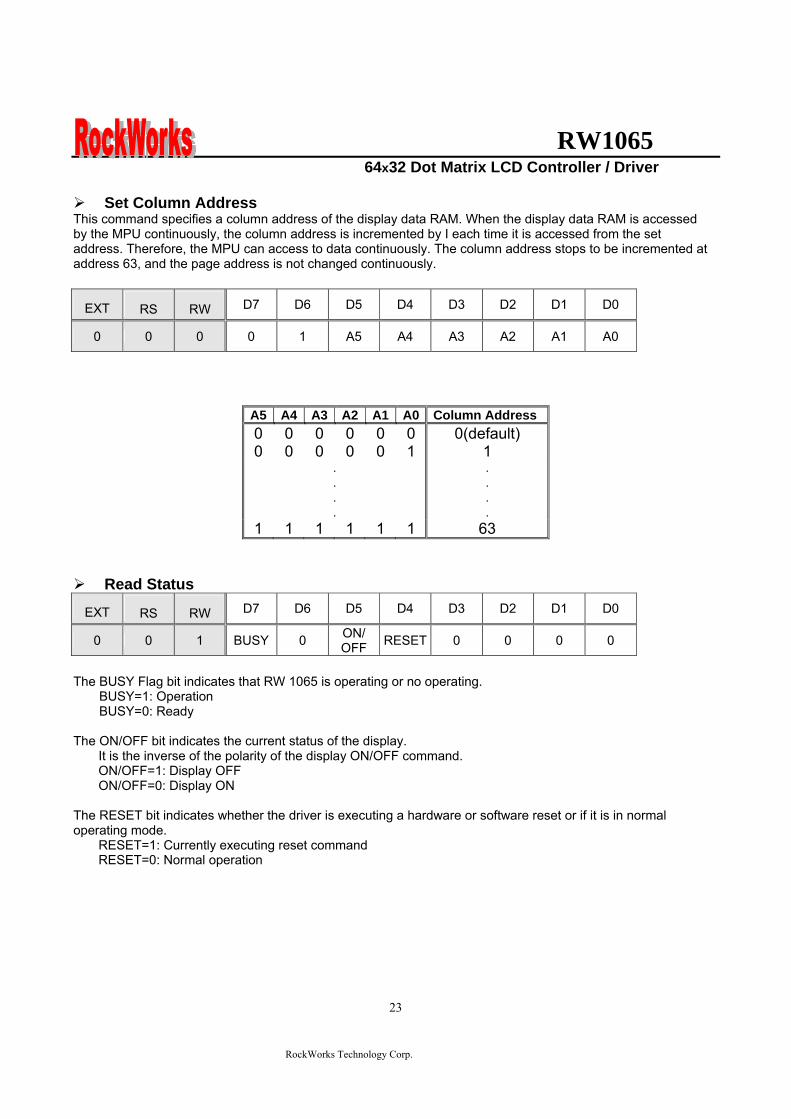
RW1065 64x32 Dot Matrix LCD Controller Driver
RockWorks Technology Corp
23
Set Column Address This command specifies a column address of the display data RAM When the display data RAM is accessed by the MPU continuously the column address is incremented by I each time it is accessed from the set address Therefore the MPU can access to data continuously The column address stops to be incremented at address 63 and the page address is not changed continuously
EXT RS RW D7 D6 D5 D4 D3 D2 D1 D0
0 0 0 0 1 A5 A4 A3 A2 A1 A0
A5 A4 A3 A2 A1 A0 Column Address0 0 0 0 0 0 0(default) 0 0 0 0 0 1 1
1 1 1 1 1 1 63
Read Status
EXT RS RW D7 D6 D5 D4 D3 D2 D1 D0
0 0 1 BUSY 0 ON OFF RESET 0 0 0 0
The BUSY Flag bit indicates that RW 1065 is operating or no operating
BUSY=1 Operation BUSY=0 Ready
The ONOFF bit indicates the current status of the display It is the inverse of the polarity of the display ONOFF command ONOFF=1 Display OFF ONOFF=0 Display ON The RESET bit indicates whether the driver is executing a hardware or software reset or if it is in normal operating mode RESET=1 Currently executing reset command RESET=0 Normal operation
RW1065 64x32 Dot Matrix LCD Controller Driver
RockWorks Technology Corp
24
Write Display Data
EXT RS RW D7 D6 D5 D4 D3 D2 D1 D0
0 1 0 Write data
Writes 8-bits of data into the display data RAM at a location specified by the contents of the column address and page address registers and then increments the column address register by one
Read Display Data
EXT RS RW D7 D6 D5 D4 D3 D2 D1 D0
0 1 1 Read data
Reads 8-bits of data from the data IO latch updates the contents of the IO latch with display data from the display data RAM location specified by the contents of the column address and page address registers and then increments the column address register After loading a new address into the column address register one dummy read is required before valid data is obtained
Set initial display line register
EXT RS RW D7 D6 D5 D4 D3 D2 D1 D0
0 0 0 1 1 S5 S4 S3 S2 S1 S0
Loads the RAM line address of the initial display line COM 0 into the initial display line register The RAM display data becomes the top line of the LCD screen It is followed by the higher number lines in ascending order corresponding to the duty cycle The screen can be scrolled using this command by incrementing the line address(default value=rdquo00Hrdquo)
RW1065 64x32 Dot Matrix LCD Controller Driver
RockWorks Technology Corp
25
Read-Modify-Write
EXT RS RW D7 D6 D5 D4 D3 D2 D1 D0
1 0 0 0 0 0 0 1 0 0 0
This command defeats column address register auto-increment after data reads The current contents of the column Address register are saved The mode remains active until an End command is received When the End command is entered the column address is returned to the one used during input of Read-Modify-Write Command This function can reduce the load of MPU when data change is repeated as a specific display area Any command other than Data Read or Write can be used in the Read-Modify-Write mode However the Column Address Set command cannot be used
End
EXT RS RW D7 D6 D5 D4 D3 D2 D1 D0
1 0 0 0 0 0 0 1 1 1 0
This command cancels read-modify-write mode and restores the contents of the column address register to their value prior to the receipt of the Read-Modify-Write command
N N+1 N+2 N+3 N+m N
Read -modify-write mode set End
Returm
Column address
Set page address
Set column address
Read-modify-write
Dummy read
Read data
Write data
End
CompletedNo
Yes
RW1065 64x32 Dot Matrix LCD Controller Driver
RockWorks Technology Corp
26
Set power save mode
EXT RS RW D7 D6 D5 D4 D3 D2 D1 D0
1 0 0 0 0 0 0 0 0 1 PSAVE
When power save mode is entered thus greatly reducing power consumption In the power save mode the display data is saved as is the operating mode that was in effect before the power saver mode was initiated and the MPU is still able to access the display data RAM PSAVE=1 Sleep mode PSAVE=0 Normal mode Sleep mode This stops all operations in the LCD display system and as long as there are no accesses from the MPU the consumption current is reduced to a value near the static current The internal modes during sleep mode are as follows 1 The oscillator circuit and the LCD power supply circuit are halted 2 All liquid crystal drive circuits are halted and the segment and common drive outputs output a Vss level
Display command double command
EXT RS RW D7 D6 D5 D4 D3 D2 D1 D0
1 0 0 0 0 0 0 0 1 0 1
1 0 0 FRSEL 0 0 0 0 REV ALLON DUTY
Display NormalReverse set REV=1 Reverse REV=0 Normal(default) Display All Point ONOFF ALLON=1 All display points ON ALLON=0 Normal(default) Select Duty Duty=1 164 duty cycle(default) Duty=0 132 duty cycle FRAME FREQUENCY Select FRSEL=1 Double FRSEL=0 (default)
RW1065 64x32 Dot Matrix LCD Controller Driver
RockWorks Technology Corp
27
Hardware Pin Set
Select ADC by ADC Pin The pin selects the relationship between display data RAM column addresses and segment drivers ADC=1 SEG0larrcolumn address 3FHhellipinverted ADC=0 SEG0larrcolumn address 00Hhellipnormal(default) This command is provided to reduce restrictions on the placement of driver ICs and routing of traces during printed circuit Board design See Figure 4 for a table of segments and column addresses for the two values of D
Select SHL by SHL Pin The pin selects the com output scan direction SHL=1 Reverse directioncom63rarrcom0 SHL=0 Normal com0rarrcom63 Both master and slave should set identical SHL value
Select LCD Bias by BS0 BS1 Pin
BS1 BS0 Bias 0 0 15 bias 0 1 16 bias 1 0 18 bias 1 1 19 bias
RW1065 64x32 Dot Matrix LCD Controller Driver
RockWorks Technology Corp
28
When an External Resistance is Used The liquid crystal power supply voltage V0 is set by adding resistors Rarsquo and Rbrsquo between VDD and VR and between VR and V0 respectively
RW1065
RW1065 64x32 Dot Matrix LCD Controller Driver
RockWorks Technology Corp
29
The set voltage circuits
Using the step-up voltage circuits equipped within the RW1065 chips it is possible to produce a 2X 3X 4X step-up voltage levels 2X step-up
To produce voltage level in the positive direction at the Vout terminal that is 2 times the voltage difference between VSS and VDD2 Please configure set voltage circuits like this Place a 1uF~22uF capacitor between CAP1N and CAP1P Place a 1uF~22uF capacitor between VSS and VOUT Short CAP2P CAP3P and VOUT Leave CAP2N open 3X step-up
To produce voltage level in the positive direction at the Vout terminal that is 3 times the voltage difference between VSS and VDD2 Please configure set voltage circuits like this Place a 1uF~22uF capacitor between CAP1N and CAP1P Place a 1uF~22uF capacitor between VSS and VOUT Place a 1uF~22uF capacitor and 100 ohms resistor between CAP2N and CAP2P Short CAP3P and Vout 4X step-up
To produce voltage level in the positive direction at the Vout terminal that is 4 times the voltage difference between VSS and VDD2 Please configure set voltage circuits like this Place a 1uF~22uF capacitor between CAP1N and CAP1P Place a 1uF~22uF capacitor between VSS and VOUT Place a 1uF~22uF capacitor and 100 ohms resistor between CAP2N and CAP2P Place a 1uF~22uF capacitor and 100 ohms resistor between CAP1N and CAP3P
RW1065 64x32 Dot Matrix LCD Controller Driver
RockWorks Technology Corp
30
ABSOLUTE MAXIMUM RATINGS Characteristics Symbol Value Unit
Power supply voltage VDD -03 to +70 V
LCD driver voltage Vout 0 to +17 V
Input voltage VIN -03 to VDD+03 V
Operating temperature TA -40 to +85
Storage temperature TSTO -55 to +125
DC CHARACTERISTICS
Rating Item Symbol Condition Min Typ Max Unit ApplicablePin
Operating Voltage VDD - 27 30 55 V VDD1
Step up output voltage Vout (Relative to VDD) 0 - 17 V Vout
Voltage follower circuit operating Voltage V0 (Relative to VDD) 0 - 15 V V0
V0 accuracy V0 - 0 - 15 V0
High-level Input Voltage Low-level Input Voltage
VIHC VILC - 07 VDD
Vss - VDD 09 V 2
High-level Output Voltage Low-level Output Voltage
VOHC VOLC
IOH = ndash05 mA IOL = 05 mA
08VDD Vss - VDD
02 VDD V 3
Input leakage current ILI VIN = VDD or VSS -1 - 2 uA 4
Output leakage current ILO - -1 1 uA 5
Liquid Crystal Driver ON Resistance RON
Ta= 25degC(Relative To VDD)
V0 =15 V - 16 20 KΩ SEGn COMn 6
Internal Oscillator fOSC 2286 254 2794 Oscillator
Frequency External Input RECOMMAND fCL
Ta = 25degC 132Duty 2286 254 2794
kHz CL
Internal Oscillator fOSC 45 5 55 Oscillator
Frequency External Input RECOMMAND fCL
Ta = 25degC 164Duty 45 5 55
kHz CL
bullDynamic Consumption Current During Display with the Internal Power Supply OFF Current consumed by total ICs when an external power supply is used
Unless otherwise specified Vss=0V VDD=30V
RW1065 64x32 Dot Matrix LCD Controller Driver
RockWorks Technology Corp
31
Display Pattern OFF
Ta = 25degC Vout=17V Rating Item Symbol Condition Min Typ Max Unit Notes
VDD=30 V V0-Vss=8V - 10 15 RW1065 IDD VDD=50 V V0-Vss=8V - 35 45
microA 7
Display Pattern Checker
Ta = 25degC Vout=17V Rating Item Symbol Condition Min Typ Max Unit Notes
VDD=30 V V0-Vss=8V - 15 20 RW1065 IDD VDD=50 V V0-Vss=8V - 40 50
microA 7
Display Pattern OFF
Ta = 25degC Vout=17V Rating Item Symbol Condition Min Typ Max Unit Notes
VDD=30 V V0-Vss=8V - 15 20 RW1065 IDD VDD=50 V V0-Vss=8V - 40 50
microA 7
Display pattern Checker
Ta = 25degC Vout=17V Rating Item Symbol Condition Min Typ Max Unit Notes
VDD=30 V V0-Vss=8V - 65 80 RW1065 IDD VDD=50 V V0-Vss=8V - 130 150
microA 7
bull Consumption Current at Time of Power Saver Mode VSS = 0 V VDD = 30 V plusmn 10
Rating Item Symbol Condition Min Typ Max Unit Notes
Sleep mode IDD - - 5 10 microA -
References for items market with 1 While a broad range of operating voltages is guaranteed performance cannot be guaranteed if there are sudden fluctuations to the
voltage while the MPU is being accessed 2 The RS D0 to D5 D6 D7 E RW CS1BP CS2P CLS CL FR MS and RST
― terminals
3 The D0 to D7 FR and CL terminals 4 The RS E RW CS1BP CS2P CLS MS and RST
― terminals
5 Applies when the D0 to D5 D6 D7 CL and FR terminals are in a high impedance state 6 These are the resistance values for when a 01 V voltage is applied between the output terminals SEGn or COMn and
the various power supply terminals (V1 V2 V3 and V4) These are specified for the operating voltage (3) range RON = 01 V ∆I (Where ∆I is the current that flows when 01 V is applied while the power supply is ON)
7 It indicates the current consumed on ICs alone when the internal oscillator circuit and display are turned on Does not include the current due to the LCD panel capacity and wiring capacity Applicable only when there is no access from the MPU
RW1065 64x32 Dot Matrix LCD Controller Driver
RockWorks Technology Corp
32
TIMING CHARACTERISTICS
68 Interface
(Ta=-40 to 85 degC) VDD=27 to 45V
Rating VDD=45 to 55V
Rating Item Signal Symbol ConditionMin Max Min Max
Units
Address hold time RS tAH6 0 mdash 0 mdash Address setup time RS tAW6
mdash 0 mdash 0 mdash
ns
System cycle time RS tCYC6 mdash 900 mdash 800 mdash ns Data setup time D0 to D7 tDS6 100 mdash 100 mdash Data hold time D0 to D7 tDH6
mdash 0 mdash 0 mdash
ns
Access time D0 to D7 tACC6 mdash 350 mdash 250
Output disable time D0 to D7 tOH6 CL = 100 pF
mdash 300 mdash 200 ns
Read tEWHR 360 mdash 300 mdash Enable H pulse time
WriteE
tEWHW mdash
360 mdash 300 mdash ns
Read tEWLR 450 mdash 400 mdash Enable L pulse time
WriteE
tEWLW mdash
450 mdash 400 mdash ns
1 All timing is specified using 20 and 80 of VDD as the reference 2 tEWLW and tEWLR are specified as the overlap between CS1BP being ldquoLrdquo (CS2P = ldquoHrdquo) and E
RW1065 64x32 Dot Matrix LCD Controller Driver
RockWorks Technology Corp
33
Reset Timing
Rating Item Signal Symbol Condition
Min Typ Max Units
Reset time mdash tR mdash mdash - 2 micros
Reset ldquoLrdquo pulse width RST tRW mdash 2 - mdash micros
1 When double chip was be used then the duty set command must be set between the tR
RW1065 64x32 Dot Matrix LCD Controller Driver
RockWorks Technology Corp
34
IO PAD CONFIGURATION
RW1065 64x32 Dot Matrix LCD Controller Driver
RockWorks Technology Corp
35
THE MPU INTERFACE (REFERENCE EXAMPLES) The RW1065 Series can be connected to 6800 Series MPUs The display area can be enlarged by using multiple RW1065 Series chips When this is done the chip select signal can be used to select the individual ICs to access
6800 Series MPUs
RW
106
5
RW1065 64x32 Dot Matrix LCD Controller Driver
RockWorks Technology Corp
36
When using external multi-level power supply for LCD driving (REFERENCE EXAMPLE)
Using a resistor divider can provide RW1065 external multi-level power supply for LCD driving
The circuit below shows a resistor divider network which can bias V0 V1 V2 V3 and V4 externally
RW1065 64x32 Dot Matrix LCD Controller Driver
RockWorks Technology Corp
37
bullWhen V0 V1 V2 V3 and V4 are biased by external power supply analog section of RW1065 should be turn off by software during LCD initialization The example in below shows the sequence to turn off analog section when external bias is used Begin of LCD initialization 1 Reset RW1065 2 SET EXT=1 (mode instruction)
RS RW DB7 DB6 DB5 DB4 DB3 DB2 DB1 DB00 0 0 0 0 0 1 1 0 1
3 SET Display Command (double command)
RS RW DB7 DB6 DB5 DB4 DB3 DB2 DB1 DB00 0 0 0 0 0 0 1 0 1 0 0 0 0 1 1 0 0 0 1
4 SET EXT=1 (mode instruction)
RS RW DB7 DB6 DB5 DB4 DB3 DB2 DB1 DB00 0 0 0 0 0 1 1 0 0
End of LCD initialization
bullBecause pins can not set LCD bias when external power supplies are used for LCD driving the bias can be set by an appropriate configuration for a resistor voltage divider networks The example is shown below
VSS
R
R
NR
R
R
RV1
RV2
RV3
RV4
V0
Bias Network Circuit Concept 15 Bias N=1 total = 5R 16 Bias N=2 total =6R 18 Bias N=4 total =8R 19 Bias N=5 total = 9R
RW1065 64x32 Dot Matrix LCD Controller Driver
RockWorks Technology Corp
38
Single chip solution for RW1065 application (REFERENCE EXAMPLE)
For a 64x32 application the duty cycle of LCD panel is 164 and the display duty of RW1065 should be set to 164 The display duty cycle can be selected by the DUTY bit in display command The diagram for 64x32 application is shown below
64 SEGx32COM LCD Panel
164 duty cycle
RW1065 DUTY=1
COM1~33
SEG1~65
RW1065 64x32 Dot Matrix LCD Controller Driver
RockWorks Technology Corp
39
Using an adjustable resistor on the main board to adjust the contrast of liquid crystal display (REFERENCE EXAMPLE)
The schematic shows an adjustable resistor on main board that can adjust voltage level of V0
RW1065 64x32 Dot Matrix LCD Controller Driver
RockWorks Technology Corp
40
Package information (Please pay close attention to the information in this section Do not hesitate to consult with our sale representative if you have any question or concern)
In order to make better bonding yield for RW1065 please follow the tips and recommendations in this section In this section few tips about COB footprint style PCB layout and wire bonding will be discussed
The drawing in below shows the PCB footprint style which we recommend for RW1065 Pads array in
curve shape is easier for Al wire bonding Besides that a real size COB footprint for RW1065 is also shown in below RW1065 COB footprint is also available in powerpcb or protel format for design reference purpose
The ratio is 11
RW1065 64x32 Dot Matrix LCD Controller Driver
RockWorks Technology Corp
41
During COB footprint design there have some tips about footprint that the PCB designer should know The angle between bonding wire and vertical line should less than 45 Otherwise the wire shorts would become very easy to happen at fours corners of the chip
The angle between bonding wire and vertical line could be reduced by expanding the distance between pads array and the chip In addition reducing length in horizon direction of pads array could minimize the angle between bonding wire and vertical line The picture in below will help to illustrate this concept From the experiences COB footprint style affects the bonding yield
Bad Wires are too close to each other
The angle between bonding wire and vertical line is greater than 45
The angle between bonding wire and vertical line is less than 45
Wires are not too close to each other
Reducing length in horizon direction of pads array could minimize the angle between bonding wire and vertical line
The angle between bonding wire and vertical line could be reduced by expanding the distance between pads array and the chip
RW1065 64x32 Dot Matrix LCD Controller Driver
RockWorks Technology Corp
42
If the gap between pads of COB footprint is filled with solder mask coating it is difficult to bond Al wire to
the pads The top solder masks layer that overlap COB footprint area should be removed
Please use 1 mils diameter Al wire for RW1065 wire bonding
1 2 3 4 5 6
A
B
C
D
654321
D
C
B
A
Title
Number RevisionSize
C
Date 29-Aug-2007 Sheet of File D公司資料99seMyDesignddb Drawn By
RW1065
COM131
COM142
COM153
COM164
COM175
COM186
COM197
COM208
COM219
COM2210
COM2311
COM2412
COM2513
COM2614
COM2715
COM2816
COM2917
COM3018
COM3119
SEG
6320
SEG
6221
SEG
6122
SEG
6023
SEG
5924
SEG
5825
SEG
5726
SEG
5627
SEG
5528
SEG
5429
SEG
5330
SEG
5231
SEG
5132
SEG
5033
SEG
4934
SEG
4835
SEG
4736
SEG
4637
SEG
4538
SEG
4439
SEG
4340
SEG
4241
SEG
4142
SEG
4043
SEG
3944
SEG
3845
SEG
3746
SEG
3647
SEG
3548
SEG
3449
SEG
3350
SEG
3251
SEG
3152
SEG
3053
SEG
2954
SEG
2855
SEG
2756
SEG
2657
SEG
2558
SEG
2459
SEG
2360
SEG
2261
SEG
2162
SEG
2063
SEG
1964
SEG
1865
SEG
1766
SEG
1667
SEG
1568
SEG
1469
SEG13 70SEG12 71SEG11 72SEG10 73SEG9 74SEG8 75SEG7 76SEG6 77SEG5 78SEG4 79SEG3 80SEG2 81SEG1 82SEG0 83ADCP 84CLL 85
VSS
86D
087
D1
88D
289
D3
90D
491
D5
92D
693
D7
94C
S1B
P95
CS2
P96
ERD
P97
AO
P(R
S)98
RW
RP
99V
DD
100
RST
P10
1C
LSP
102
FRR
103
MSP
104
BS1
P10
5B
S0P
106
SHLP
107
VD
D2
108
CA
P2N
109
CA
P2P
110
CA
P1P
111
CA
P1N
112
CA
P3P
113
VO
UT
114
V0
115
VR
AB
116
V3
117
V2
118
V4
119
V1
120
CO
M0
121
CO
M1
122
CO
M2
123
CO
M3
124
CO
M4
125
CO
M5
126
CO
M6
127
CO
M7
128
CO
M8
129
CO
M9
130
CO
M10
131
CO
M11
132
CO
M12
133
4897x1902 um
IC1
RW1065
C9CAPR4
100R0603
R30R0603
C8
CAP
C7
CAP
R2
100R0603
R1
0R0603C6 22uf
R50R
R6300R
R7RES1
R8NC R9
100R0603
VDD
R10
NC
R11
100R0603
R12
100R0603
R13
NC
R14
100R0603
R15
NC
VDD
D0
D1
D2
D3
D4
D5
D6
D7
DB[07]
VDDC5
01uf0603
VD
D
CS2
P
123456789
1011121314151617181920
J1
CON20
C1201uf0603
R3951K0603
VDD
CAP Value1UF~22UF
2XPut C6C8 Short R1R3Open R2R4C7C93XPut C6C8C9 R4Short R1Open R2R3C74XOpen R1R3
BS0 BS1 Bias0 0
0 1
1 0
11
15 bias
16 bias
18 bias
19 bias
ADC=0 SEG0lt~column address 00Hnormal(default) ADC=1 SEG0lt~column address 3FHinverted
SHL=0 Normal COM0~gtCOM63(default)SHL=1 Reverse direction COM63~gtCOM0
R16100R0603
LCD PANEL 64X32RockWorks
RW1065 64X32
COM0-31 SEG0-63SHL=0 ADC=0
SHL=1COM31-0
ADC=1SEG63-0
if use single chip for 32 command displaythe display command must select 164 dutyDisplay panel must select 164 duty type
VO
UT
C3P
C1N
C1P
C2P
C2N
VDD2
ADC
SHL
BS0
BS1
CLLADC
V1
V2
V3
V4
VR
AB
V0
VO
UT
C3P
C1N
C1P
C2P
C2N
VD
D2
SHL
BS0
BS1
FRR
RST
P
RW
RS
E CS1
B
CS1
V0RSRWED0D1D2D3D4D5D6D7
RSTPAK
C4
22uf
RBRES1
RA1RES1
C2
22uf
C1
22uf
C3
22uf
C0
22uf
R20
100k0603
R21
100k0603
R17
200K0603
V1
V2
V3
V4 VRAB
V0
V0
OPTION
B
R18
300R0603
RA2RES1
VADJ
R19100R
R23 RES1R22 0R
R24
RES1
R25
0R
VDD
CS1BP
CS2P
CS1
CS1
R26
22R0603
R27
22R0603
C1047uf
C11
01uf
VSS_INVDD_IN
D1DIODE
FGND
鐵框地
VSS
VDD
R28 10RR29 10RR30 10RR31 10RR32 10RR33 10RR34 10RR35 10RR36 10RR37 10RR38 10R
VADJ
1 2 3 4 5 6
A
B
C
D
654321
D
C
B
A
Title
Number RevisionSize
C
Date 29-Aug-2007 Sheet of File D公司資料99seMyDesignddb Drawn By
RW1065
COM131
COM142
COM153
COM164
COM175
COM186
COM197
COM208
COM219
COM2210
COM2311
COM2412
COM2513
COM2614
COM2715
COM2816
COM2917
COM3018
COM3119
SEG
6320
SEG
6221
SEG
6122
SEG
6023
SEG
5924
SEG
5825
SEG
5726
SEG
5627
SEG
5528
SEG
5429
SEG
5330
SEG
5231
SEG
5132
SEG
5033
SEG
4934
SEG
4835
SEG
4736
SEG
4637
SEG
4538
SEG
4439
SEG
4340
SEG
4241
SEG
4142
SEG
4043
SEG
3944
SEG
3845
SEG
3746
SEG
3647
SEG
3548
SEG
3449
SEG
3350
SEG
3251
SEG
3152
SEG
3053
SEG
2954
SEG
2855
SEG
2756
SEG
2657
SEG
2558
SEG
2459
SEG
2360
SEG
2261
SEG
2162
SEG
2063
SEG
1964
SEG
1865
SEG
1766
SEG
1667
SEG
1568
SEG
1469
SEG13 70SEG12 71SEG11 72SEG10 73SEG9 74SEG8 75SEG7 76SEG6 77SEG5 78SEG4 79SEG3 80SEG2 81SEG1 82SEG0 83ADCP 84CLL 85
VSS
86D
087
D1
88D
289
D3
90D
491
D5
92D
693
D7
94C
S1B
P95
CS2
P96
ERD
P97
AO
P(R
S)98
RW
RP
99V
DD
100
RST
P10
1C
LSP
102
FRR
103
MSP
104
BS1
P10
5B
S0P
106
SHLP
107
VD
D2
108
CA
P2N
109
CA
P2P
110
CA
P1P
111
CA
P1N
112
CA
P3P
113
VO
UT
114
V0
115
VR
AB
116
V3
117
V2
118
V4
119
V1
120
CO
M0
121
CO
M1
122
CO
M2
123
CO
M3
124
CO
M4
125
CO
M5
126
CO
M6
127
CO
M7
128
CO
M8
129
CO
M9
130
CO
M10
131
CO
M11
132
CO
M12
133
4897x1902 um
IC1
RW1065 Master
RW1065
COM131
COM142
COM153
COM164
COM175
COM186
COM197
COM208
COM219
COM2210
COM2311
COM2412
COM2513
COM2614
COM2715
COM2816
COM2917
COM3018
COM3119
SEG
6320
SEG
6221
SEG
6122
SEG
6023
SEG
5924
SEG
5825
SEG
5726
SEG
5627
SEG
5528
SEG
5429
SEG
5330
SEG
5231
SEG
5132
SEG
5033
SEG
4934
SEG
4835
SEG
4736
SEG
4637
SEG
4538
SEG
4439
SEG
4340
SEG
4241
SEG
4142
SEG
4043
SEG
3944
SEG
3845
SEG
3746
SEG
3647
SEG
3548
SEG
3449
SEG
3350
SEG
3251
SEG
3152
SEG
3053
SEG
2954
SEG
2855
SEG
2756
SEG
2657
SEG
2558
SEG
2459
SEG
2360
SEG
2261
SEG
2162
SEG
2063
SEG
1964
SEG
1865
SEG
1766
SEG
1667
SEG
1568
SEG
1469
SEG13 70SEG12 71SEG11 72SEG10 73SEG9 74SEG8 75SEG7 76SEG6 77SEG5 78SEG4 79SEG3 80SEG2 81SEG1 82SEG0 83ADCP 84CLL 85
VSS
86D
087
D1
88D
289
D3
90D
491
D5
92D
693
D7
94C
S1B
P95
CS2
P96
ERD
P97
AO
P(R
S)98
RW
RP
99V
DD
100
RST
P10
1C
LSP
102
FRR
103
MSP
104
BS1
P10
5B
S0P
106
SHLP
107
VD
D2
108
CA
P2N
109
CA
P2P
110
CA
P1P
111
CA
P1N
112
CA
P3P
113
VO
UT
114
V0
115
VR
AB
116
V3
117
V2
118
V4
119
V1
120
CO
M0
121
CO
M1
122
CO
M2
123
CO
M3
124
CO
M4
125
CO
M5
126
CO
M6
127
CO
M7
128
CO
M8
129
CO
M9
130
CO
M10
131
CO
M11
132
CO
M12
133
4897x1902 um
IC2
RW1065 Slave
C4
22uf
RBRES1
RA1RES1
C2
22uf
C1
22uf
C3
22uf
C0
22ufC9CAPR4
100R0603
R30R0603
C8
CAP
C7
CAP
R2
100R0603
R1
0R0603C6 22uf
R50R0603
R6300R0603
R7RES1
R8NC R9
100R0603
VDD
R10
NC
R11
100R0603
R12
NC
R13
100R0603
R14
100R0603
R15
NC
R16
100R0603
R17
NC
VDD
D0
D1
D2
D3
D4
D5
D6
D7
D0
D1
D2
D3
D4
D5
D6
D7
DB[07] DB[07]
VDDC10
01uf0603
VD
D
IC1_
CS2
P
VDD
IC2_
CS2
P
VD
D
C11
01uf0603
VSS
VSS
LCD PANEL 128X64
Master COM0-31 Slave COM32-63
Master SEG0-63 Slave SEG64-127
123456789
1011121314151617181920
J1
CON20
Master Slave
CAP Value1UF~22UF
2XPut C6C8 Short R1R3Open R2R4C7C93XPut C6C8C9 R4Short R1Open R2R3C74XOpen R1R3
RockWorksRW1065 128x64
BS0 BS1 Bias0 0
0 1
1 0
11
15 bias
16 bias
18 bias
19 bias
ADC=0 SEG0lt~column address 00Hnormal(default) ADC=1 SEG0lt~column address 3FHinverted
SHL=0 Normal COM0~gtCOM63(default)SHL=1 Reverse direction COM63~gtCOM0Both Master and Slave should set identical SHL value
SHL=0 SHL=0
ADC=0 ADC=0
Slave COM31-0
Slave SEG127-64
SHL=1
ADC=1
SHL=1Master COM63-32
ADC=1Master SEG63-0
R18100R0603
R22
100k0603
R23
100k0603
C501uF0603
R4551K0603
VDD
R19
200K0603
ADC1
ADC2
SHL
BS0
BS1
VDD2
V1
V2
V3
V4 VRAB
V0
V0V
OU
T
C3P
C1N
C1P
C2P
C2N
V1
V2
V3
V4
VR
AB
V0
VO
UT
C3P
C1N
C1P
C2P
C2N
VD
D2
SHL
BS0
BS1
FRR
RST
P
RW
RS
E IC1_
CS1
BP
V1
V2
V3
V4
VR
AB
V0
VO
UT
VD
D2
SHL
BS0
BS1
FRR
RST
P
RW
RS
E IC2_
CS1
BP
CLLADC1
CLLADC2
RSTP
CS1CS2
V0RSRWED0D1D2D3D4D5D6D7
AK
OPTION
R20
300R0603
RA2RES1
VADJ
R21
100R
B
R25 RESR24 0R
R26 RES R27 0RVDD
IC1_CS1BP
IC1_CS2P
CS1
CS1
R28 0R R29 RES
R30 RES R31 0R
IC2_CS1BP
IC2_CS2P
CS2
CS2
R32
22R0603
R33
22R0603
C1001uf
C11
47uf
D1DIODE
FGND
鐵框地
VSS
VDD
R34 10RR35 10RR36 10RR37 10RR38 10RR39 10RR40 10RR41 10RR42 10RR43 10RR44 10R
VSS_INVDD_IN
VADJ
VDD
1 2 3 4 5 6 7 8
A
B
C
D
87654321
D
C
B
A
Title
Number RevisionSize
D
Date 29-Aug-2007 Sheet of File D公司資料 99seMyDesignddb Drawn By
C422uf
RBRES1
RA1RES1
C3
22uf
C2
22uf
C1
22uf
C0
22ufC9CAPR4
100R0603
R30R0603
C8
CAP
C7
CAP
R2
100R0603
R1
0R0603C6 22uf
R220R0603
R23300R0603
R24RES1
R39
NCR40
100 ohm0603
VDD
R41
NC
R42
100 ohm0603
R43
NC
R44
100 ohm0603
R45
NC
R46
100 ohm0603
R47
100 ohm0603
R48
NC
R49
100 ohm0603
R50
NC
VDDCAP Value1UF~22UF
2XPut C6C8 Short R1R3Open R2R4C7C93XPut C6C8C9 R4Short R1Open R2R3C74XOpen R1R3
BS0 BS1 Bias0 0
0 1
1 0
11
15 bias
16 bias
18 bias
19 bias
ADC=0 SEG0lt~column address 00Hnormal(default)
ADC=1 SEG0lt~column address 3FHinverted
SHL=0 Normal COM0~gtCOM63(default)SHL=1 Reverse direction COM63~gtCOM0Both Master and Slave should set identical SHL value
R7
100k0603
R8
100k0603
V1
V2
V3
V4
V0
VRAB
V0
R5
200K
VDD2
VO
UT
C3P
C1N
C1P
C2P
C2N
ADC1
ADC2
ADC3
SHL
BS0
BS1
CS1CS2CS3
V0RSRWED0D1D2D3D4D5D6D7
RSTP
R3851K0603
C5
01uF
VDD
OPTION
R6
300R0603R9100R
RA2RES1
VADJ
RW1065
COM131
COM142
COM153
COM164
COM175
COM186
COM197
COM208
COM219
COM2210
COM2311
COM2412
COM2513
COM2614
COM2715
COM2816
COM2917
COM3018
COM3119
SEG
6320
SEG
6221
SEG
6122
SEG
6023
SEG
5924
SEG
5825
SEG
5726
SEG
5627
SEG
5528
SEG
5429
SEG
5330
SEG
5231
SEG
5132
SEG
5033
SEG
4934
SEG
4835
SEG
4736
SEG
4637
SEG
4538
SEG
4439
SEG
4340
SEG
4241
SEG
4142
SEG
4043
SEG
3944
SEG
3845
SEG
3746
SEG
3647
SEG
3548
SEG
3449
SEG
3350
SEG
3251
SEG
3152
SEG
3053
SEG
2954
SEG
2855
SEG
2756
SEG
2657
SEG
2558
SEG
2459
SEG
2360
SEG
2261
SEG
2162
SEG
2063
SEG
1964
SEG
1865
SEG
1766
SEG
1667
SEG
1568
SEG
1469
SEG13 70SEG12 71SEG11 72SEG10 73SEG9 74SEG8 75SEG7 76SEG6 77SEG5 78SEG4 79SEG3 80SEG2 81SEG1 82SEG0 83ADCP 84CLL 85
VSS
86D
087
D1
88D
289
D3
90D
491
D5
92D
693
D7
94C
S1B
P95
CS2
P96
ERD
P97
AO
P(R
S)98
RW
RP
99V
DD
100
RST
P10
1C
LSP
102
FRR
103
MSP
104
BS1
P10
5B
S0P
106
SHLP
107
VD
D2
108
CA
P2N
109
CA
P2P
110
CA
P1P
111
CA
P1N
112
CA
P3P
113
VO
UT
114
V0
115
VR
AB
116
V3
117
V2
118
V4
119
V1
120
CO
M0
121
CO
M1
122
CO
M2
123
CO
M3
124
CO
M4
125
CO
M5
126
CO
M6
127
CO
M7
128
CO
M8
129
CO
M9
130
CO
M10
131
CO
M11
132
CO
M12
133
4897x1902 um
IC1
RW1065 Master
RW1065
COM131
COM142
COM153
COM164
COM175
COM186
COM197
COM208
COM219
COM2210
COM2311
COM2412
COM2513
COM2614
COM2715
COM2816
COM2917
COM3018
COM3119
SEG
6320
SEG
6221
SEG
6122
SEG
6023
SEG
5924
SEG
5825
SEG
5726
SEG
5627
SEG
5528
SEG
5429
SEG
5330
SEG
5231
SEG
5132
SEG
5033
SEG
4934
SEG
4835
SEG
4736
SEG
4637
SEG
4538
SEG
4439
SEG
4340
SEG
4241
SEG
4142
SEG
4043
SEG
3944
SEG
3845
SEG
3746
SEG
3647
SEG
3548
SEG
3449
SEG
3350
SEG
3251
SEG
3152
SEG
3053
SEG
2954
SEG
2855
SEG
2756
SEG
2657
SEG
2558
SEG
2459
SEG
2360
SEG
2261
SEG
2162
SEG
2063
SEG
1964
SEG
1865
SEG
1766
SEG
1667
SEG
1568
SEG
1469
SEG13 70SEG12 71SEG11 72SEG10 73SEG9 74SEG8 75SEG7 76SEG6 77SEG5 78SEG4 79SEG3 80SEG2 81SEG1 82SEG0 83ADCP 84CLL 85
VSS
86D
087
D1
88D
289
D3
90D
491
D5
92D
693
D7
94C
S1B
P95
CS2
P96
ERD
P97
AO
P(R
S)98
RW
RP
99V
DD
100
RST
P10
1C
LSP
102
FRR
103
MSP
104
BS1
P10
5B
S0P
106
SHLP
107
VD
D2
108
CA
P2N
109
CA
P2P
110
CA
P1P
111
CA
P1N
112
CA
P3P
113
VO
UT
114
V0
115
VR
AB
116
V3
117
V2
118
V4
119
V1
120
CO
M0
121
CO
M1
122
CO
M2
123
CO
M3
124
CO
M4
125
CO
M5
126
CO
M6
127
CO
M7
128
CO
M8
129
CO
M9
130
CO
M10
131
CO
M11
132
CO
M12
133
4897x1902 um
IC2
RW1065 Slave
D0
D1
D2
D3
D4
D5
D6
D7
D0
D1
D2
D3
D4
D5
D6
D7
DB[07] DB[07]
VDDC8
01uf0603
VD
D
VDD
VD
D
C9
01uf0603
VSS
VSS
LCD PANEL 192X64
Master COM0-31 Slave COM32-63
Master SEG0-63 Slave SEG64-127
Master Slave
RockWorksRW1065 192x64
RW1065
COM131
COM142
COM153
COM164
COM175
COM186
COM197
COM208
COM219
COM2210
COM2311
COM2412
COM2513
COM2614
COM2715
COM2816
COM2917
COM3018
COM3119
SEG
6320
SEG
6221
SEG
6122
SEG
6023
SEG
5924
SEG
5825
SEG
5726
SEG
5627
SEG
5528
SEG
5429
SEG
5330
SEG
5231
SEG
5132
SEG
5033
SEG
4934
SEG
4835
SEG
4736
SEG
4637
SEG
4538
SEG
4439
SEG
4340
SEG
4241
SEG
4142
SEG
4043
SEG
3944
SEG
3845
SEG
3746
SEG
3647
SEG
3548
SEG
3449
SEG
3350
SEG
3251
SEG
3152
SEG
3053
SEG
2954
SEG
2855
SEG
2756
SEG
2657
SEG
2558
SEG
2459
SEG
2360
SEG
2261
SEG
2162
SEG
2063
SEG
1964
SEG
1865
SEG
1766
SEG
1667
SEG
1568
SEG
1469
SEG13 70SEG12 71SEG11 72SEG10 73SEG9 74SEG8 75SEG7 76SEG6 77SEG5 78SEG4 79SEG3 80SEG2 81SEG1 82SEG0 83ADCP 84CLL 85
VSS
86D
087
D1
88D
289
D3
90D
491
D5
92D
693
D7
94C
S1B
P95
CS2
P96
ERD
P97
AO
P(R
S)98
RW
RP
99V
DD
100
RST
P10
1C
LSP
102
FRR
103
MSP
104
BS1
P10
5B
S0P
106
SHLP
107
VD
D2
108
CA
P2N
109
CA
P2P
110
CA
P1P
111
CA
P1N
112
CA
P3P
113
VO
UT
114
V0
115
VR
AB
116
V3
117
V2
118
V4
119
V1
120
CO
M0
121
CO
M1
122
CO
M2
123
CO
M3
124
CO
M4
125
CO
M5
126
CO
M6
127
CO
M7
128
CO
M8
129
CO
M9
130
CO
M10
131
CO
M11
132
CO
M12
133
4897x1902 um
IC3
RW1065 Slave
D0
D1
D2
D3
D4
D5
D6
D7
DB[07]
VSS
VSS
VDD
VD
D
C10
01uf0603
Slave SEG128-192
Slave
SHL=0 SHL=0
Master COM63-32SHL=1 SHL=1
Slave COM31-0ADC=0 ADC=0 ADC=0
ADC=1 ADC=1 ADC=1Master SEG63-0 Slave SEG127-64 Slave SEG192-128
R50100R0603
V1
V2
V3
V4
VR
AB
V0
VO
UT
C3P
C1N
C1P
C2P
C2N
VD
D2
SHL
BS0
BS1
FRR
RST
P
RW
RS
E V1
V2
V3
V4
VR
AB
V0
VO
UT
VD
D2
SHL
BS0
BS1
FRR
RST
P
RW
RS
E V1
V2
V3
V4
VR
AB
V0
VO
UT
VD
D2
SHL
BS0
BS1
FRR
RST
P
RW
RS
E
CLL CLL CLLADC1 ADC2 ADC3
R25 10RR26 10RR27 10RR28 10RR29 10RR30 10RR31 10RR32 10RR33 10RR34 10RR35 10R
R36
22R0603
D1DIODE
R3722R0603
C647uf
C701uf
VSS_INVDD_IN
VSS
VDD
VADJ
123456789
101112131415161718192021222324
J1
CON24
AK
FGND
鐵框地
IC1_
CS1
BP
IC1_
CS2
P
IC2_
CS2
PIC
2_C
S1B
P
IC3_
CS1
BP
IC3_
CS2
B
R10 0R R11 RES
R12 RES R13 0RVDD
IC1_CS2B
IC1_CS1BPCS1
CS1
R14 0R R15 RES
R16 RES R17 0RVDDIC2_CS2B
IC2_CS1BPCS2
CS2
R18 0R R19 RES
R20 RES R21 0RVDDIC3_CS2B
IC3_CS1BPCS3
CS3
B
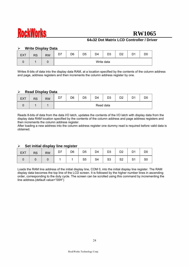
RW1065 64x32 Dot Matrix LCD Controller Driver
RockWorks Technology Corp
24
Write Display Data
EXT RS RW D7 D6 D5 D4 D3 D2 D1 D0
0 1 0 Write data
Writes 8-bits of data into the display data RAM at a location specified by the contents of the column address and page address registers and then increments the column address register by one
Read Display Data
EXT RS RW D7 D6 D5 D4 D3 D2 D1 D0
0 1 1 Read data
Reads 8-bits of data from the data IO latch updates the contents of the IO latch with display data from the display data RAM location specified by the contents of the column address and page address registers and then increments the column address register After loading a new address into the column address register one dummy read is required before valid data is obtained
Set initial display line register
EXT RS RW D7 D6 D5 D4 D3 D2 D1 D0
0 0 0 1 1 S5 S4 S3 S2 S1 S0
Loads the RAM line address of the initial display line COM 0 into the initial display line register The RAM display data becomes the top line of the LCD screen It is followed by the higher number lines in ascending order corresponding to the duty cycle The screen can be scrolled using this command by incrementing the line address(default value=rdquo00Hrdquo)
RW1065 64x32 Dot Matrix LCD Controller Driver
RockWorks Technology Corp
25
Read-Modify-Write
EXT RS RW D7 D6 D5 D4 D3 D2 D1 D0
1 0 0 0 0 0 0 1 0 0 0
This command defeats column address register auto-increment after data reads The current contents of the column Address register are saved The mode remains active until an End command is received When the End command is entered the column address is returned to the one used during input of Read-Modify-Write Command This function can reduce the load of MPU when data change is repeated as a specific display area Any command other than Data Read or Write can be used in the Read-Modify-Write mode However the Column Address Set command cannot be used
End
EXT RS RW D7 D6 D5 D4 D3 D2 D1 D0
1 0 0 0 0 0 0 1 1 1 0
This command cancels read-modify-write mode and restores the contents of the column address register to their value prior to the receipt of the Read-Modify-Write command
N N+1 N+2 N+3 N+m N
Read -modify-write mode set End
Returm
Column address
Set page address
Set column address
Read-modify-write
Dummy read
Read data
Write data
End
CompletedNo
Yes
RW1065 64x32 Dot Matrix LCD Controller Driver
RockWorks Technology Corp
26
Set power save mode
EXT RS RW D7 D6 D5 D4 D3 D2 D1 D0
1 0 0 0 0 0 0 0 0 1 PSAVE
When power save mode is entered thus greatly reducing power consumption In the power save mode the display data is saved as is the operating mode that was in effect before the power saver mode was initiated and the MPU is still able to access the display data RAM PSAVE=1 Sleep mode PSAVE=0 Normal mode Sleep mode This stops all operations in the LCD display system and as long as there are no accesses from the MPU the consumption current is reduced to a value near the static current The internal modes during sleep mode are as follows 1 The oscillator circuit and the LCD power supply circuit are halted 2 All liquid crystal drive circuits are halted and the segment and common drive outputs output a Vss level
Display command double command
EXT RS RW D7 D6 D5 D4 D3 D2 D1 D0
1 0 0 0 0 0 0 0 1 0 1
1 0 0 FRSEL 0 0 0 0 REV ALLON DUTY
Display NormalReverse set REV=1 Reverse REV=0 Normal(default) Display All Point ONOFF ALLON=1 All display points ON ALLON=0 Normal(default) Select Duty Duty=1 164 duty cycle(default) Duty=0 132 duty cycle FRAME FREQUENCY Select FRSEL=1 Double FRSEL=0 (default)
RW1065 64x32 Dot Matrix LCD Controller Driver
RockWorks Technology Corp
27
Hardware Pin Set
Select ADC by ADC Pin The pin selects the relationship between display data RAM column addresses and segment drivers ADC=1 SEG0larrcolumn address 3FHhellipinverted ADC=0 SEG0larrcolumn address 00Hhellipnormal(default) This command is provided to reduce restrictions on the placement of driver ICs and routing of traces during printed circuit Board design See Figure 4 for a table of segments and column addresses for the two values of D
Select SHL by SHL Pin The pin selects the com output scan direction SHL=1 Reverse directioncom63rarrcom0 SHL=0 Normal com0rarrcom63 Both master and slave should set identical SHL value
Select LCD Bias by BS0 BS1 Pin
BS1 BS0 Bias 0 0 15 bias 0 1 16 bias 1 0 18 bias 1 1 19 bias
RW1065 64x32 Dot Matrix LCD Controller Driver
RockWorks Technology Corp
28
When an External Resistance is Used The liquid crystal power supply voltage V0 is set by adding resistors Rarsquo and Rbrsquo between VDD and VR and between VR and V0 respectively
RW1065
RW1065 64x32 Dot Matrix LCD Controller Driver
RockWorks Technology Corp
29
The set voltage circuits
Using the step-up voltage circuits equipped within the RW1065 chips it is possible to produce a 2X 3X 4X step-up voltage levels 2X step-up
To produce voltage level in the positive direction at the Vout terminal that is 2 times the voltage difference between VSS and VDD2 Please configure set voltage circuits like this Place a 1uF~22uF capacitor between CAP1N and CAP1P Place a 1uF~22uF capacitor between VSS and VOUT Short CAP2P CAP3P and VOUT Leave CAP2N open 3X step-up
To produce voltage level in the positive direction at the Vout terminal that is 3 times the voltage difference between VSS and VDD2 Please configure set voltage circuits like this Place a 1uF~22uF capacitor between CAP1N and CAP1P Place a 1uF~22uF capacitor between VSS and VOUT Place a 1uF~22uF capacitor and 100 ohms resistor between CAP2N and CAP2P Short CAP3P and Vout 4X step-up
To produce voltage level in the positive direction at the Vout terminal that is 4 times the voltage difference between VSS and VDD2 Please configure set voltage circuits like this Place a 1uF~22uF capacitor between CAP1N and CAP1P Place a 1uF~22uF capacitor between VSS and VOUT Place a 1uF~22uF capacitor and 100 ohms resistor between CAP2N and CAP2P Place a 1uF~22uF capacitor and 100 ohms resistor between CAP1N and CAP3P
RW1065 64x32 Dot Matrix LCD Controller Driver
RockWorks Technology Corp
30
ABSOLUTE MAXIMUM RATINGS Characteristics Symbol Value Unit
Power supply voltage VDD -03 to +70 V
LCD driver voltage Vout 0 to +17 V
Input voltage VIN -03 to VDD+03 V
Operating temperature TA -40 to +85
Storage temperature TSTO -55 to +125
DC CHARACTERISTICS
Rating Item Symbol Condition Min Typ Max Unit ApplicablePin
Operating Voltage VDD - 27 30 55 V VDD1
Step up output voltage Vout (Relative to VDD) 0 - 17 V Vout
Voltage follower circuit operating Voltage V0 (Relative to VDD) 0 - 15 V V0
V0 accuracy V0 - 0 - 15 V0
High-level Input Voltage Low-level Input Voltage
VIHC VILC - 07 VDD
Vss - VDD 09 V 2
High-level Output Voltage Low-level Output Voltage
VOHC VOLC
IOH = ndash05 mA IOL = 05 mA
08VDD Vss - VDD
02 VDD V 3
Input leakage current ILI VIN = VDD or VSS -1 - 2 uA 4
Output leakage current ILO - -1 1 uA 5
Liquid Crystal Driver ON Resistance RON
Ta= 25degC(Relative To VDD)
V0 =15 V - 16 20 KΩ SEGn COMn 6
Internal Oscillator fOSC 2286 254 2794 Oscillator
Frequency External Input RECOMMAND fCL
Ta = 25degC 132Duty 2286 254 2794
kHz CL
Internal Oscillator fOSC 45 5 55 Oscillator
Frequency External Input RECOMMAND fCL
Ta = 25degC 164Duty 45 5 55
kHz CL
bullDynamic Consumption Current During Display with the Internal Power Supply OFF Current consumed by total ICs when an external power supply is used
Unless otherwise specified Vss=0V VDD=30V
RW1065 64x32 Dot Matrix LCD Controller Driver
RockWorks Technology Corp
31
Display Pattern OFF
Ta = 25degC Vout=17V Rating Item Symbol Condition Min Typ Max Unit Notes
VDD=30 V V0-Vss=8V - 10 15 RW1065 IDD VDD=50 V V0-Vss=8V - 35 45
microA 7
Display Pattern Checker
Ta = 25degC Vout=17V Rating Item Symbol Condition Min Typ Max Unit Notes
VDD=30 V V0-Vss=8V - 15 20 RW1065 IDD VDD=50 V V0-Vss=8V - 40 50
microA 7
Display Pattern OFF
Ta = 25degC Vout=17V Rating Item Symbol Condition Min Typ Max Unit Notes
VDD=30 V V0-Vss=8V - 15 20 RW1065 IDD VDD=50 V V0-Vss=8V - 40 50
microA 7
Display pattern Checker
Ta = 25degC Vout=17V Rating Item Symbol Condition Min Typ Max Unit Notes
VDD=30 V V0-Vss=8V - 65 80 RW1065 IDD VDD=50 V V0-Vss=8V - 130 150
microA 7
bull Consumption Current at Time of Power Saver Mode VSS = 0 V VDD = 30 V plusmn 10
Rating Item Symbol Condition Min Typ Max Unit Notes
Sleep mode IDD - - 5 10 microA -
References for items market with 1 While a broad range of operating voltages is guaranteed performance cannot be guaranteed if there are sudden fluctuations to the
voltage while the MPU is being accessed 2 The RS D0 to D5 D6 D7 E RW CS1BP CS2P CLS CL FR MS and RST
― terminals
3 The D0 to D7 FR and CL terminals 4 The RS E RW CS1BP CS2P CLS MS and RST
― terminals
5 Applies when the D0 to D5 D6 D7 CL and FR terminals are in a high impedance state 6 These are the resistance values for when a 01 V voltage is applied between the output terminals SEGn or COMn and
the various power supply terminals (V1 V2 V3 and V4) These are specified for the operating voltage (3) range RON = 01 V ∆I (Where ∆I is the current that flows when 01 V is applied while the power supply is ON)
7 It indicates the current consumed on ICs alone when the internal oscillator circuit and display are turned on Does not include the current due to the LCD panel capacity and wiring capacity Applicable only when there is no access from the MPU
RW1065 64x32 Dot Matrix LCD Controller Driver
RockWorks Technology Corp
32
TIMING CHARACTERISTICS
68 Interface
(Ta=-40 to 85 degC) VDD=27 to 45V
Rating VDD=45 to 55V
Rating Item Signal Symbol ConditionMin Max Min Max
Units
Address hold time RS tAH6 0 mdash 0 mdash Address setup time RS tAW6
mdash 0 mdash 0 mdash
ns
System cycle time RS tCYC6 mdash 900 mdash 800 mdash ns Data setup time D0 to D7 tDS6 100 mdash 100 mdash Data hold time D0 to D7 tDH6
mdash 0 mdash 0 mdash
ns
Access time D0 to D7 tACC6 mdash 350 mdash 250
Output disable time D0 to D7 tOH6 CL = 100 pF
mdash 300 mdash 200 ns
Read tEWHR 360 mdash 300 mdash Enable H pulse time
WriteE
tEWHW mdash
360 mdash 300 mdash ns
Read tEWLR 450 mdash 400 mdash Enable L pulse time
WriteE
tEWLW mdash
450 mdash 400 mdash ns
1 All timing is specified using 20 and 80 of VDD as the reference 2 tEWLW and tEWLR are specified as the overlap between CS1BP being ldquoLrdquo (CS2P = ldquoHrdquo) and E
RW1065 64x32 Dot Matrix LCD Controller Driver
RockWorks Technology Corp
33
Reset Timing
Rating Item Signal Symbol Condition
Min Typ Max Units
Reset time mdash tR mdash mdash - 2 micros
Reset ldquoLrdquo pulse width RST tRW mdash 2 - mdash micros
1 When double chip was be used then the duty set command must be set between the tR
RW1065 64x32 Dot Matrix LCD Controller Driver
RockWorks Technology Corp
34
IO PAD CONFIGURATION
RW1065 64x32 Dot Matrix LCD Controller Driver
RockWorks Technology Corp
35
THE MPU INTERFACE (REFERENCE EXAMPLES) The RW1065 Series can be connected to 6800 Series MPUs The display area can be enlarged by using multiple RW1065 Series chips When this is done the chip select signal can be used to select the individual ICs to access
6800 Series MPUs
RW
106
5
RW1065 64x32 Dot Matrix LCD Controller Driver
RockWorks Technology Corp
36
When using external multi-level power supply for LCD driving (REFERENCE EXAMPLE)
Using a resistor divider can provide RW1065 external multi-level power supply for LCD driving
The circuit below shows a resistor divider network which can bias V0 V1 V2 V3 and V4 externally
RW1065 64x32 Dot Matrix LCD Controller Driver
RockWorks Technology Corp
37
bullWhen V0 V1 V2 V3 and V4 are biased by external power supply analog section of RW1065 should be turn off by software during LCD initialization The example in below shows the sequence to turn off analog section when external bias is used Begin of LCD initialization 1 Reset RW1065 2 SET EXT=1 (mode instruction)
RS RW DB7 DB6 DB5 DB4 DB3 DB2 DB1 DB00 0 0 0 0 0 1 1 0 1
3 SET Display Command (double command)
RS RW DB7 DB6 DB5 DB4 DB3 DB2 DB1 DB00 0 0 0 0 0 0 1 0 1 0 0 0 0 1 1 0 0 0 1
4 SET EXT=1 (mode instruction)
RS RW DB7 DB6 DB5 DB4 DB3 DB2 DB1 DB00 0 0 0 0 0 1 1 0 0
End of LCD initialization
bullBecause pins can not set LCD bias when external power supplies are used for LCD driving the bias can be set by an appropriate configuration for a resistor voltage divider networks The example is shown below
VSS
R
R
NR
R
R
RV1
RV2
RV3
RV4
V0
Bias Network Circuit Concept 15 Bias N=1 total = 5R 16 Bias N=2 total =6R 18 Bias N=4 total =8R 19 Bias N=5 total = 9R
RW1065 64x32 Dot Matrix LCD Controller Driver
RockWorks Technology Corp
38
Single chip solution for RW1065 application (REFERENCE EXAMPLE)
For a 64x32 application the duty cycle of LCD panel is 164 and the display duty of RW1065 should be set to 164 The display duty cycle can be selected by the DUTY bit in display command The diagram for 64x32 application is shown below
64 SEGx32COM LCD Panel
164 duty cycle
RW1065 DUTY=1
COM1~33
SEG1~65
RW1065 64x32 Dot Matrix LCD Controller Driver
RockWorks Technology Corp
39
Using an adjustable resistor on the main board to adjust the contrast of liquid crystal display (REFERENCE EXAMPLE)
The schematic shows an adjustable resistor on main board that can adjust voltage level of V0
RW1065 64x32 Dot Matrix LCD Controller Driver
RockWorks Technology Corp
40
Package information (Please pay close attention to the information in this section Do not hesitate to consult with our sale representative if you have any question or concern)
In order to make better bonding yield for RW1065 please follow the tips and recommendations in this section In this section few tips about COB footprint style PCB layout and wire bonding will be discussed
The drawing in below shows the PCB footprint style which we recommend for RW1065 Pads array in
curve shape is easier for Al wire bonding Besides that a real size COB footprint for RW1065 is also shown in below RW1065 COB footprint is also available in powerpcb or protel format for design reference purpose
The ratio is 11
RW1065 64x32 Dot Matrix LCD Controller Driver
RockWorks Technology Corp
41
During COB footprint design there have some tips about footprint that the PCB designer should know The angle between bonding wire and vertical line should less than 45 Otherwise the wire shorts would become very easy to happen at fours corners of the chip
The angle between bonding wire and vertical line could be reduced by expanding the distance between pads array and the chip In addition reducing length in horizon direction of pads array could minimize the angle between bonding wire and vertical line The picture in below will help to illustrate this concept From the experiences COB footprint style affects the bonding yield
Bad Wires are too close to each other
The angle between bonding wire and vertical line is greater than 45
The angle between bonding wire and vertical line is less than 45
Wires are not too close to each other
Reducing length in horizon direction of pads array could minimize the angle between bonding wire and vertical line
The angle between bonding wire and vertical line could be reduced by expanding the distance between pads array and the chip
RW1065 64x32 Dot Matrix LCD Controller Driver
RockWorks Technology Corp
42
If the gap between pads of COB footprint is filled with solder mask coating it is difficult to bond Al wire to
the pads The top solder masks layer that overlap COB footprint area should be removed
Please use 1 mils diameter Al wire for RW1065 wire bonding
1 2 3 4 5 6
A
B
C
D
654321
D
C
B
A
Title
Number RevisionSize
C
Date 29-Aug-2007 Sheet of File D公司資料99seMyDesignddb Drawn By
RW1065
COM131
COM142
COM153
COM164
COM175
COM186
COM197
COM208
COM219
COM2210
COM2311
COM2412
COM2513
COM2614
COM2715
COM2816
COM2917
COM3018
COM3119
SEG
6320
SEG
6221
SEG
6122
SEG
6023
SEG
5924
SEG
5825
SEG
5726
SEG
5627
SEG
5528
SEG
5429
SEG
5330
SEG
5231
SEG
5132
SEG
5033
SEG
4934
SEG
4835
SEG
4736
SEG
4637
SEG
4538
SEG
4439
SEG
4340
SEG
4241
SEG
4142
SEG
4043
SEG
3944
SEG
3845
SEG
3746
SEG
3647
SEG
3548
SEG
3449
SEG
3350
SEG
3251
SEG
3152
SEG
3053
SEG
2954
SEG
2855
SEG
2756
SEG
2657
SEG
2558
SEG
2459
SEG
2360
SEG
2261
SEG
2162
SEG
2063
SEG
1964
SEG
1865
SEG
1766
SEG
1667
SEG
1568
SEG
1469
SEG13 70SEG12 71SEG11 72SEG10 73SEG9 74SEG8 75SEG7 76SEG6 77SEG5 78SEG4 79SEG3 80SEG2 81SEG1 82SEG0 83ADCP 84CLL 85
VSS
86D
087
D1
88D
289
D3
90D
491
D5
92D
693
D7
94C
S1B
P95
CS2
P96
ERD
P97
AO
P(R
S)98
RW
RP
99V
DD
100
RST
P10
1C
LSP
102
FRR
103
MSP
104
BS1
P10
5B
S0P
106
SHLP
107
VD
D2
108
CA
P2N
109
CA
P2P
110
CA
P1P
111
CA
P1N
112
CA
P3P
113
VO
UT
114
V0
115
VR
AB
116
V3
117
V2
118
V4
119
V1
120
CO
M0
121
CO
M1
122
CO
M2
123
CO
M3
124
CO
M4
125
CO
M5
126
CO
M6
127
CO
M7
128
CO
M8
129
CO
M9
130
CO
M10
131
CO
M11
132
CO
M12
133
4897x1902 um
IC1
RW1065
C9CAPR4
100R0603
R30R0603
C8
CAP
C7
CAP
R2
100R0603
R1
0R0603C6 22uf
R50R
R6300R
R7RES1
R8NC R9
100R0603
VDD
R10
NC
R11
100R0603
R12
100R0603
R13
NC
R14
100R0603
R15
NC
VDD
D0
D1
D2
D3
D4
D5
D6
D7
DB[07]
VDDC5
01uf0603
VD
D
CS2
P
123456789
1011121314151617181920
J1
CON20
C1201uf0603
R3951K0603
VDD
CAP Value1UF~22UF
2XPut C6C8 Short R1R3Open R2R4C7C93XPut C6C8C9 R4Short R1Open R2R3C74XOpen R1R3
BS0 BS1 Bias0 0
0 1
1 0
11
15 bias
16 bias
18 bias
19 bias
ADC=0 SEG0lt~column address 00Hnormal(default) ADC=1 SEG0lt~column address 3FHinverted
SHL=0 Normal COM0~gtCOM63(default)SHL=1 Reverse direction COM63~gtCOM0
R16100R0603
LCD PANEL 64X32RockWorks
RW1065 64X32
COM0-31 SEG0-63SHL=0 ADC=0
SHL=1COM31-0
ADC=1SEG63-0
if use single chip for 32 command displaythe display command must select 164 dutyDisplay panel must select 164 duty type
VO
UT
C3P
C1N
C1P
C2P
C2N
VDD2
ADC
SHL
BS0
BS1
CLLADC
V1
V2
V3
V4
VR
AB
V0
VO
UT
C3P
C1N
C1P
C2P
C2N
VD
D2
SHL
BS0
BS1
FRR
RST
P
RW
RS
E CS1
B
CS1
V0RSRWED0D1D2D3D4D5D6D7
RSTPAK
C4
22uf
RBRES1
RA1RES1
C2
22uf
C1
22uf
C3
22uf
C0
22uf
R20
100k0603
R21
100k0603
R17
200K0603
V1
V2
V3
V4 VRAB
V0
V0
OPTION
B
R18
300R0603
RA2RES1
VADJ
R19100R
R23 RES1R22 0R
R24
RES1
R25
0R
VDD
CS1BP
CS2P
CS1
CS1
R26
22R0603
R27
22R0603
C1047uf
C11
01uf
VSS_INVDD_IN
D1DIODE
FGND
鐵框地
VSS
VDD
R28 10RR29 10RR30 10RR31 10RR32 10RR33 10RR34 10RR35 10RR36 10RR37 10RR38 10R
VADJ
1 2 3 4 5 6
A
B
C
D
654321
D
C
B
A
Title
Number RevisionSize
C
Date 29-Aug-2007 Sheet of File D公司資料99seMyDesignddb Drawn By
RW1065
COM131
COM142
COM153
COM164
COM175
COM186
COM197
COM208
COM219
COM2210
COM2311
COM2412
COM2513
COM2614
COM2715
COM2816
COM2917
COM3018
COM3119
SEG
6320
SEG
6221
SEG
6122
SEG
6023
SEG
5924
SEG
5825
SEG
5726
SEG
5627
SEG
5528
SEG
5429
SEG
5330
SEG
5231
SEG
5132
SEG
5033
SEG
4934
SEG
4835
SEG
4736
SEG
4637
SEG
4538
SEG
4439
SEG
4340
SEG
4241
SEG
4142
SEG
4043
SEG
3944
SEG
3845
SEG
3746
SEG
3647
SEG
3548
SEG
3449
SEG
3350
SEG
3251
SEG
3152
SEG
3053
SEG
2954
SEG
2855
SEG
2756
SEG
2657
SEG
2558
SEG
2459
SEG
2360
SEG
2261
SEG
2162
SEG
2063
SEG
1964
SEG
1865
SEG
1766
SEG
1667
SEG
1568
SEG
1469
SEG13 70SEG12 71SEG11 72SEG10 73SEG9 74SEG8 75SEG7 76SEG6 77SEG5 78SEG4 79SEG3 80SEG2 81SEG1 82SEG0 83ADCP 84CLL 85
VSS
86D
087
D1
88D
289
D3
90D
491
D5
92D
693
D7
94C
S1B
P95
CS2
P96
ERD
P97
AO
P(R
S)98
RW
RP
99V
DD
100
RST
P10
1C
LSP
102
FRR
103
MSP
104
BS1
P10
5B
S0P
106
SHLP
107
VD
D2
108
CA
P2N
109
CA
P2P
110
CA
P1P
111
CA
P1N
112
CA
P3P
113
VO
UT
114
V0
115
VR
AB
116
V3
117
V2
118
V4
119
V1
120
CO
M0
121
CO
M1
122
CO
M2
123
CO
M3
124
CO
M4
125
CO
M5
126
CO
M6
127
CO
M7
128
CO
M8
129
CO
M9
130
CO
M10
131
CO
M11
132
CO
M12
133
4897x1902 um
IC1
RW1065 Master
RW1065
COM131
COM142
COM153
COM164
COM175
COM186
COM197
COM208
COM219
COM2210
COM2311
COM2412
COM2513
COM2614
COM2715
COM2816
COM2917
COM3018
COM3119
SEG
6320
SEG
6221
SEG
6122
SEG
6023
SEG
5924
SEG
5825
SEG
5726
SEG
5627
SEG
5528
SEG
5429
SEG
5330
SEG
5231
SEG
5132
SEG
5033
SEG
4934
SEG
4835
SEG
4736
SEG
4637
SEG
4538
SEG
4439
SEG
4340
SEG
4241
SEG
4142
SEG
4043
SEG
3944
SEG
3845
SEG
3746
SEG
3647
SEG
3548
SEG
3449
SEG
3350
SEG
3251
SEG
3152
SEG
3053
SEG
2954
SEG
2855
SEG
2756
SEG
2657
SEG
2558
SEG
2459
SEG
2360
SEG
2261
SEG
2162
SEG
2063
SEG
1964
SEG
1865
SEG
1766
SEG
1667
SEG
1568
SEG
1469
SEG13 70SEG12 71SEG11 72SEG10 73SEG9 74SEG8 75SEG7 76SEG6 77SEG5 78SEG4 79SEG3 80SEG2 81SEG1 82SEG0 83ADCP 84CLL 85
VSS
86D
087
D1
88D
289
D3
90D
491
D5
92D
693
D7
94C
S1B
P95
CS2
P96
ERD
P97
AO
P(R
S)98
RW
RP
99V
DD
100
RST
P10
1C
LSP
102
FRR
103
MSP
104
BS1
P10
5B
S0P
106
SHLP
107
VD
D2
108
CA
P2N
109
CA
P2P
110
CA
P1P
111
CA
P1N
112
CA
P3P
113
VO
UT
114
V0
115
VR
AB
116
V3
117
V2
118
V4
119
V1
120
CO
M0
121
CO
M1
122
CO
M2
123
CO
M3
124
CO
M4
125
CO
M5
126
CO
M6
127
CO
M7
128
CO
M8
129
CO
M9
130
CO
M10
131
CO
M11
132
CO
M12
133
4897x1902 um
IC2
RW1065 Slave
C4
22uf
RBRES1
RA1RES1
C2
22uf
C1
22uf
C3
22uf
C0
22ufC9CAPR4
100R0603
R30R0603
C8
CAP
C7
CAP
R2
100R0603
R1
0R0603C6 22uf
R50R0603
R6300R0603
R7RES1
R8NC R9
100R0603
VDD
R10
NC
R11
100R0603
R12
NC
R13
100R0603
R14
100R0603
R15
NC
R16
100R0603
R17
NC
VDD
D0
D1
D2
D3
D4
D5
D6
D7
D0
D1
D2
D3
D4
D5
D6
D7
DB[07] DB[07]
VDDC10
01uf0603
VD
D
IC1_
CS2
P
VDD
IC2_
CS2
P
VD
D
C11
01uf0603
VSS
VSS
LCD PANEL 128X64
Master COM0-31 Slave COM32-63
Master SEG0-63 Slave SEG64-127
123456789
1011121314151617181920
J1
CON20
Master Slave
CAP Value1UF~22UF
2XPut C6C8 Short R1R3Open R2R4C7C93XPut C6C8C9 R4Short R1Open R2R3C74XOpen R1R3
RockWorksRW1065 128x64
BS0 BS1 Bias0 0
0 1
1 0
11
15 bias
16 bias
18 bias
19 bias
ADC=0 SEG0lt~column address 00Hnormal(default) ADC=1 SEG0lt~column address 3FHinverted
SHL=0 Normal COM0~gtCOM63(default)SHL=1 Reverse direction COM63~gtCOM0Both Master and Slave should set identical SHL value
SHL=0 SHL=0
ADC=0 ADC=0
Slave COM31-0
Slave SEG127-64
SHL=1
ADC=1
SHL=1Master COM63-32
ADC=1Master SEG63-0
R18100R0603
R22
100k0603
R23
100k0603
C501uF0603
R4551K0603
VDD
R19
200K0603
ADC1
ADC2
SHL
BS0
BS1
VDD2
V1
V2
V3
V4 VRAB
V0
V0V
OU
T
C3P
C1N
C1P
C2P
C2N
V1
V2
V3
V4
VR
AB
V0
VO
UT
C3P
C1N
C1P
C2P
C2N
VD
D2
SHL
BS0
BS1
FRR
RST
P
RW
RS
E IC1_
CS1
BP
V1
V2
V3
V4
VR
AB
V0
VO
UT
VD
D2
SHL
BS0
BS1
FRR
RST
P
RW
RS
E IC2_
CS1
BP
CLLADC1
CLLADC2
RSTP
CS1CS2
V0RSRWED0D1D2D3D4D5D6D7
AK
OPTION
R20
300R0603
RA2RES1
VADJ
R21
100R
B
R25 RESR24 0R
R26 RES R27 0RVDD
IC1_CS1BP
IC1_CS2P
CS1
CS1
R28 0R R29 RES
R30 RES R31 0R
IC2_CS1BP
IC2_CS2P
CS2
CS2
R32
22R0603
R33
22R0603
C1001uf
C11
47uf
D1DIODE
FGND
鐵框地
VSS
VDD
R34 10RR35 10RR36 10RR37 10RR38 10RR39 10RR40 10RR41 10RR42 10RR43 10RR44 10R
VSS_INVDD_IN
VADJ
VDD
1 2 3 4 5 6 7 8
A
B
C
D
87654321
D
C
B
A
Title
Number RevisionSize
D
Date 29-Aug-2007 Sheet of File D公司資料 99seMyDesignddb Drawn By
C422uf
RBRES1
RA1RES1
C3
22uf
C2
22uf
C1
22uf
C0
22ufC9CAPR4
100R0603
R30R0603
C8
CAP
C7
CAP
R2
100R0603
R1
0R0603C6 22uf
R220R0603
R23300R0603
R24RES1
R39
NCR40
100 ohm0603
VDD
R41
NC
R42
100 ohm0603
R43
NC
R44
100 ohm0603
R45
NC
R46
100 ohm0603
R47
100 ohm0603
R48
NC
R49
100 ohm0603
R50
NC
VDDCAP Value1UF~22UF
2XPut C6C8 Short R1R3Open R2R4C7C93XPut C6C8C9 R4Short R1Open R2R3C74XOpen R1R3
BS0 BS1 Bias0 0
0 1
1 0
11
15 bias
16 bias
18 bias
19 bias
ADC=0 SEG0lt~column address 00Hnormal(default)
ADC=1 SEG0lt~column address 3FHinverted
SHL=0 Normal COM0~gtCOM63(default)SHL=1 Reverse direction COM63~gtCOM0Both Master and Slave should set identical SHL value
R7
100k0603
R8
100k0603
V1
V2
V3
V4
V0
VRAB
V0
R5
200K
VDD2
VO
UT
C3P
C1N
C1P
C2P
C2N
ADC1
ADC2
ADC3
SHL
BS0
BS1
CS1CS2CS3
V0RSRWED0D1D2D3D4D5D6D7
RSTP
R3851K0603
C5
01uF
VDD
OPTION
R6
300R0603R9100R
RA2RES1
VADJ
RW1065
COM131
COM142
COM153
COM164
COM175
COM186
COM197
COM208
COM219
COM2210
COM2311
COM2412
COM2513
COM2614
COM2715
COM2816
COM2917
COM3018
COM3119
SEG
6320
SEG
6221
SEG
6122
SEG
6023
SEG
5924
SEG
5825
SEG
5726
SEG
5627
SEG
5528
SEG
5429
SEG
5330
SEG
5231
SEG
5132
SEG
5033
SEG
4934
SEG
4835
SEG
4736
SEG
4637
SEG
4538
SEG
4439
SEG
4340
SEG
4241
SEG
4142
SEG
4043
SEG
3944
SEG
3845
SEG
3746
SEG
3647
SEG
3548
SEG
3449
SEG
3350
SEG
3251
SEG
3152
SEG
3053
SEG
2954
SEG
2855
SEG
2756
SEG
2657
SEG
2558
SEG
2459
SEG
2360
SEG
2261
SEG
2162
SEG
2063
SEG
1964
SEG
1865
SEG
1766
SEG
1667
SEG
1568
SEG
1469
SEG13 70SEG12 71SEG11 72SEG10 73SEG9 74SEG8 75SEG7 76SEG6 77SEG5 78SEG4 79SEG3 80SEG2 81SEG1 82SEG0 83ADCP 84CLL 85
VSS
86D
087
D1
88D
289
D3
90D
491
D5
92D
693
D7
94C
S1B
P95
CS2
P96
ERD
P97
AO
P(R
S)98
RW
RP
99V
DD
100
RST
P10
1C
LSP
102
FRR
103
MSP
104
BS1
P10
5B
S0P
106
SHLP
107
VD
D2
108
CA
P2N
109
CA
P2P
110
CA
P1P
111
CA
P1N
112
CA
P3P
113
VO
UT
114
V0
115
VR
AB
116
V3
117
V2
118
V4
119
V1
120
CO
M0
121
CO
M1
122
CO
M2
123
CO
M3
124
CO
M4
125
CO
M5
126
CO
M6
127
CO
M7
128
CO
M8
129
CO
M9
130
CO
M10
131
CO
M11
132
CO
M12
133
4897x1902 um
IC1
RW1065 Master
RW1065
COM131
COM142
COM153
COM164
COM175
COM186
COM197
COM208
COM219
COM2210
COM2311
COM2412
COM2513
COM2614
COM2715
COM2816
COM2917
COM3018
COM3119
SEG
6320
SEG
6221
SEG
6122
SEG
6023
SEG
5924
SEG
5825
SEG
5726
SEG
5627
SEG
5528
SEG
5429
SEG
5330
SEG
5231
SEG
5132
SEG
5033
SEG
4934
SEG
4835
SEG
4736
SEG
4637
SEG
4538
SEG
4439
SEG
4340
SEG
4241
SEG
4142
SEG
4043
SEG
3944
SEG
3845
SEG
3746
SEG
3647
SEG
3548
SEG
3449
SEG
3350
SEG
3251
SEG
3152
SEG
3053
SEG
2954
SEG
2855
SEG
2756
SEG
2657
SEG
2558
SEG
2459
SEG
2360
SEG
2261
SEG
2162
SEG
2063
SEG
1964
SEG
1865
SEG
1766
SEG
1667
SEG
1568
SEG
1469
SEG13 70SEG12 71SEG11 72SEG10 73SEG9 74SEG8 75SEG7 76SEG6 77SEG5 78SEG4 79SEG3 80SEG2 81SEG1 82SEG0 83ADCP 84CLL 85
VSS
86D
087
D1
88D
289
D3
90D
491
D5
92D
693
D7
94C
S1B
P95
CS2
P96
ERD
P97
AO
P(R
S)98
RW
RP
99V
DD
100
RST
P10
1C
LSP
102
FRR
103
MSP
104
BS1
P10
5B
S0P
106
SHLP
107
VD
D2
108
CA
P2N
109
CA
P2P
110
CA
P1P
111
CA
P1N
112
CA
P3P
113
VO
UT
114
V0
115
VR
AB
116
V3
117
V2
118
V4
119
V1
120
CO
M0
121
CO
M1
122
CO
M2
123
CO
M3
124
CO
M4
125
CO
M5
126
CO
M6
127
CO
M7
128
CO
M8
129
CO
M9
130
CO
M10
131
CO
M11
132
CO
M12
133
4897x1902 um
IC2
RW1065 Slave
D0
D1
D2
D3
D4
D5
D6
D7
D0
D1
D2
D3
D4
D5
D6
D7
DB[07] DB[07]
VDDC8
01uf0603
VD
D
VDD
VD
D
C9
01uf0603
VSS
VSS
LCD PANEL 192X64
Master COM0-31 Slave COM32-63
Master SEG0-63 Slave SEG64-127
Master Slave
RockWorksRW1065 192x64
RW1065
COM131
COM142
COM153
COM164
COM175
COM186
COM197
COM208
COM219
COM2210
COM2311
COM2412
COM2513
COM2614
COM2715
COM2816
COM2917
COM3018
COM3119
SEG
6320
SEG
6221
SEG
6122
SEG
6023
SEG
5924
SEG
5825
SEG
5726
SEG
5627
SEG
5528
SEG
5429
SEG
5330
SEG
5231
SEG
5132
SEG
5033
SEG
4934
SEG
4835
SEG
4736
SEG
4637
SEG
4538
SEG
4439
SEG
4340
SEG
4241
SEG
4142
SEG
4043
SEG
3944
SEG
3845
SEG
3746
SEG
3647
SEG
3548
SEG
3449
SEG
3350
SEG
3251
SEG
3152
SEG
3053
SEG
2954
SEG
2855
SEG
2756
SEG
2657
SEG
2558
SEG
2459
SEG
2360
SEG
2261
SEG
2162
SEG
2063
SEG
1964
SEG
1865
SEG
1766
SEG
1667
SEG
1568
SEG
1469
SEG13 70SEG12 71SEG11 72SEG10 73SEG9 74SEG8 75SEG7 76SEG6 77SEG5 78SEG4 79SEG3 80SEG2 81SEG1 82SEG0 83ADCP 84CLL 85
VSS
86D
087
D1
88D
289
D3
90D
491
D5
92D
693
D7
94C
S1B
P95
CS2
P96
ERD
P97
AO
P(R
S)98
RW
RP
99V
DD
100
RST
P10
1C
LSP
102
FRR
103
MSP
104
BS1
P10
5B
S0P
106
SHLP
107
VD
D2
108
CA
P2N
109
CA
P2P
110
CA
P1P
111
CA
P1N
112
CA
P3P
113
VO
UT
114
V0
115
VR
AB
116
V3
117
V2
118
V4
119
V1
120
CO
M0
121
CO
M1
122
CO
M2
123
CO
M3
124
CO
M4
125
CO
M5
126
CO
M6
127
CO
M7
128
CO
M8
129
CO
M9
130
CO
M10
131
CO
M11
132
CO
M12
133
4897x1902 um
IC3
RW1065 Slave
D0
D1
D2
D3
D4
D5
D6
D7
DB[07]
VSS
VSS
VDD
VD
D
C10
01uf0603
Slave SEG128-192
Slave
SHL=0 SHL=0
Master COM63-32SHL=1 SHL=1
Slave COM31-0ADC=0 ADC=0 ADC=0
ADC=1 ADC=1 ADC=1Master SEG63-0 Slave SEG127-64 Slave SEG192-128
R50100R0603
V1
V2
V3
V4
VR
AB
V0
VO
UT
C3P
C1N
C1P
C2P
C2N
VD
D2
SHL
BS0
BS1
FRR
RST
P
RW
RS
E V1
V2
V3
V4
VR
AB
V0
VO
UT
VD
D2
SHL
BS0
BS1
FRR
RST
P
RW
RS
E V1
V2
V3
V4
VR
AB
V0
VO
UT
VD
D2
SHL
BS0
BS1
FRR
RST
P
RW
RS
E
CLL CLL CLLADC1 ADC2 ADC3
R25 10RR26 10RR27 10RR28 10RR29 10RR30 10RR31 10RR32 10RR33 10RR34 10RR35 10R
R36
22R0603
D1DIODE
R3722R0603
C647uf
C701uf
VSS_INVDD_IN
VSS
VDD
VADJ
123456789
101112131415161718192021222324
J1
CON24
AK
FGND
鐵框地
IC1_
CS1
BP
IC1_
CS2
P
IC2_
CS2
PIC
2_C
S1B
P
IC3_
CS1
BP
IC3_
CS2
B
R10 0R R11 RES
R12 RES R13 0RVDD
IC1_CS2B
IC1_CS1BPCS1
CS1
R14 0R R15 RES
R16 RES R17 0RVDDIC2_CS2B
IC2_CS1BPCS2
CS2
R18 0R R19 RES
R20 RES R21 0RVDDIC3_CS2B
IC3_CS1BPCS3
CS3
B
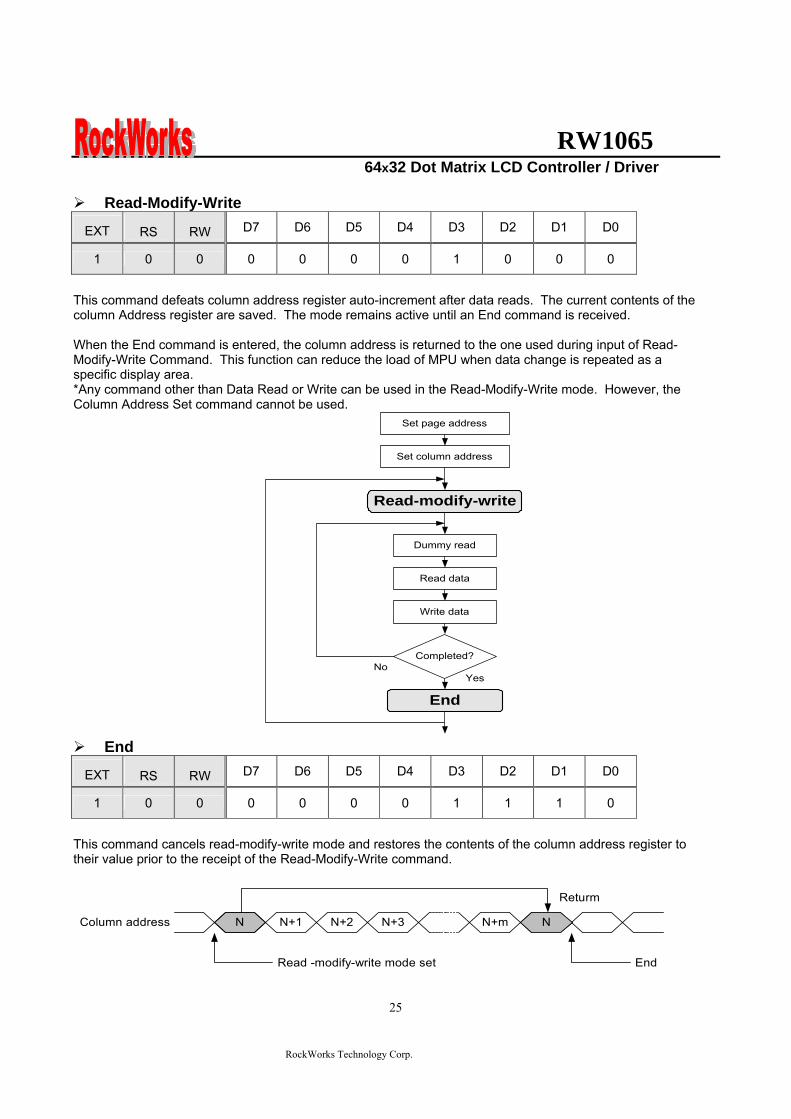
RW1065 64x32 Dot Matrix LCD Controller Driver
RockWorks Technology Corp
25
Read-Modify-Write
EXT RS RW D7 D6 D5 D4 D3 D2 D1 D0
1 0 0 0 0 0 0 1 0 0 0
This command defeats column address register auto-increment after data reads The current contents of the column Address register are saved The mode remains active until an End command is received When the End command is entered the column address is returned to the one used during input of Read-Modify-Write Command This function can reduce the load of MPU when data change is repeated as a specific display area Any command other than Data Read or Write can be used in the Read-Modify-Write mode However the Column Address Set command cannot be used
End
EXT RS RW D7 D6 D5 D4 D3 D2 D1 D0
1 0 0 0 0 0 0 1 1 1 0
This command cancels read-modify-write mode and restores the contents of the column address register to their value prior to the receipt of the Read-Modify-Write command
N N+1 N+2 N+3 N+m N
Read -modify-write mode set End
Returm
Column address
Set page address
Set column address
Read-modify-write
Dummy read
Read data
Write data
End
CompletedNo
Yes
RW1065 64x32 Dot Matrix LCD Controller Driver
RockWorks Technology Corp
26
Set power save mode
EXT RS RW D7 D6 D5 D4 D3 D2 D1 D0
1 0 0 0 0 0 0 0 0 1 PSAVE
When power save mode is entered thus greatly reducing power consumption In the power save mode the display data is saved as is the operating mode that was in effect before the power saver mode was initiated and the MPU is still able to access the display data RAM PSAVE=1 Sleep mode PSAVE=0 Normal mode Sleep mode This stops all operations in the LCD display system and as long as there are no accesses from the MPU the consumption current is reduced to a value near the static current The internal modes during sleep mode are as follows 1 The oscillator circuit and the LCD power supply circuit are halted 2 All liquid crystal drive circuits are halted and the segment and common drive outputs output a Vss level
Display command double command
EXT RS RW D7 D6 D5 D4 D3 D2 D1 D0
1 0 0 0 0 0 0 0 1 0 1
1 0 0 FRSEL 0 0 0 0 REV ALLON DUTY
Display NormalReverse set REV=1 Reverse REV=0 Normal(default) Display All Point ONOFF ALLON=1 All display points ON ALLON=0 Normal(default) Select Duty Duty=1 164 duty cycle(default) Duty=0 132 duty cycle FRAME FREQUENCY Select FRSEL=1 Double FRSEL=0 (default)
RW1065 64x32 Dot Matrix LCD Controller Driver
RockWorks Technology Corp
27
Hardware Pin Set
Select ADC by ADC Pin The pin selects the relationship between display data RAM column addresses and segment drivers ADC=1 SEG0larrcolumn address 3FHhellipinverted ADC=0 SEG0larrcolumn address 00Hhellipnormal(default) This command is provided to reduce restrictions on the placement of driver ICs and routing of traces during printed circuit Board design See Figure 4 for a table of segments and column addresses for the two values of D
Select SHL by SHL Pin The pin selects the com output scan direction SHL=1 Reverse directioncom63rarrcom0 SHL=0 Normal com0rarrcom63 Both master and slave should set identical SHL value
Select LCD Bias by BS0 BS1 Pin
BS1 BS0 Bias 0 0 15 bias 0 1 16 bias 1 0 18 bias 1 1 19 bias
RW1065 64x32 Dot Matrix LCD Controller Driver
RockWorks Technology Corp
28
When an External Resistance is Used The liquid crystal power supply voltage V0 is set by adding resistors Rarsquo and Rbrsquo between VDD and VR and between VR and V0 respectively
RW1065
RW1065 64x32 Dot Matrix LCD Controller Driver
RockWorks Technology Corp
29
The set voltage circuits
Using the step-up voltage circuits equipped within the RW1065 chips it is possible to produce a 2X 3X 4X step-up voltage levels 2X step-up
To produce voltage level in the positive direction at the Vout terminal that is 2 times the voltage difference between VSS and VDD2 Please configure set voltage circuits like this Place a 1uF~22uF capacitor between CAP1N and CAP1P Place a 1uF~22uF capacitor between VSS and VOUT Short CAP2P CAP3P and VOUT Leave CAP2N open 3X step-up
To produce voltage level in the positive direction at the Vout terminal that is 3 times the voltage difference between VSS and VDD2 Please configure set voltage circuits like this Place a 1uF~22uF capacitor between CAP1N and CAP1P Place a 1uF~22uF capacitor between VSS and VOUT Place a 1uF~22uF capacitor and 100 ohms resistor between CAP2N and CAP2P Short CAP3P and Vout 4X step-up
To produce voltage level in the positive direction at the Vout terminal that is 4 times the voltage difference between VSS and VDD2 Please configure set voltage circuits like this Place a 1uF~22uF capacitor between CAP1N and CAP1P Place a 1uF~22uF capacitor between VSS and VOUT Place a 1uF~22uF capacitor and 100 ohms resistor between CAP2N and CAP2P Place a 1uF~22uF capacitor and 100 ohms resistor between CAP1N and CAP3P
RW1065 64x32 Dot Matrix LCD Controller Driver
RockWorks Technology Corp
30
ABSOLUTE MAXIMUM RATINGS Characteristics Symbol Value Unit
Power supply voltage VDD -03 to +70 V
LCD driver voltage Vout 0 to +17 V
Input voltage VIN -03 to VDD+03 V
Operating temperature TA -40 to +85
Storage temperature TSTO -55 to +125
DC CHARACTERISTICS
Rating Item Symbol Condition Min Typ Max Unit ApplicablePin
Operating Voltage VDD - 27 30 55 V VDD1
Step up output voltage Vout (Relative to VDD) 0 - 17 V Vout
Voltage follower circuit operating Voltage V0 (Relative to VDD) 0 - 15 V V0
V0 accuracy V0 - 0 - 15 V0
High-level Input Voltage Low-level Input Voltage
VIHC VILC - 07 VDD
Vss - VDD 09 V 2
High-level Output Voltage Low-level Output Voltage
VOHC VOLC
IOH = ndash05 mA IOL = 05 mA
08VDD Vss - VDD
02 VDD V 3
Input leakage current ILI VIN = VDD or VSS -1 - 2 uA 4
Output leakage current ILO - -1 1 uA 5
Liquid Crystal Driver ON Resistance RON
Ta= 25degC(Relative To VDD)
V0 =15 V - 16 20 KΩ SEGn COMn 6
Internal Oscillator fOSC 2286 254 2794 Oscillator
Frequency External Input RECOMMAND fCL
Ta = 25degC 132Duty 2286 254 2794
kHz CL
Internal Oscillator fOSC 45 5 55 Oscillator
Frequency External Input RECOMMAND fCL
Ta = 25degC 164Duty 45 5 55
kHz CL
bullDynamic Consumption Current During Display with the Internal Power Supply OFF Current consumed by total ICs when an external power supply is used
Unless otherwise specified Vss=0V VDD=30V
RW1065 64x32 Dot Matrix LCD Controller Driver
RockWorks Technology Corp
31
Display Pattern OFF
Ta = 25degC Vout=17V Rating Item Symbol Condition Min Typ Max Unit Notes
VDD=30 V V0-Vss=8V - 10 15 RW1065 IDD VDD=50 V V0-Vss=8V - 35 45
microA 7
Display Pattern Checker
Ta = 25degC Vout=17V Rating Item Symbol Condition Min Typ Max Unit Notes
VDD=30 V V0-Vss=8V - 15 20 RW1065 IDD VDD=50 V V0-Vss=8V - 40 50
microA 7
Display Pattern OFF
Ta = 25degC Vout=17V Rating Item Symbol Condition Min Typ Max Unit Notes
VDD=30 V V0-Vss=8V - 15 20 RW1065 IDD VDD=50 V V0-Vss=8V - 40 50
microA 7
Display pattern Checker
Ta = 25degC Vout=17V Rating Item Symbol Condition Min Typ Max Unit Notes
VDD=30 V V0-Vss=8V - 65 80 RW1065 IDD VDD=50 V V0-Vss=8V - 130 150
microA 7
bull Consumption Current at Time of Power Saver Mode VSS = 0 V VDD = 30 V plusmn 10
Rating Item Symbol Condition Min Typ Max Unit Notes
Sleep mode IDD - - 5 10 microA -
References for items market with 1 While a broad range of operating voltages is guaranteed performance cannot be guaranteed if there are sudden fluctuations to the
voltage while the MPU is being accessed 2 The RS D0 to D5 D6 D7 E RW CS1BP CS2P CLS CL FR MS and RST
― terminals
3 The D0 to D7 FR and CL terminals 4 The RS E RW CS1BP CS2P CLS MS and RST
― terminals
5 Applies when the D0 to D5 D6 D7 CL and FR terminals are in a high impedance state 6 These are the resistance values for when a 01 V voltage is applied between the output terminals SEGn or COMn and
the various power supply terminals (V1 V2 V3 and V4) These are specified for the operating voltage (3) range RON = 01 V ∆I (Where ∆I is the current that flows when 01 V is applied while the power supply is ON)
7 It indicates the current consumed on ICs alone when the internal oscillator circuit and display are turned on Does not include the current due to the LCD panel capacity and wiring capacity Applicable only when there is no access from the MPU
RW1065 64x32 Dot Matrix LCD Controller Driver
RockWorks Technology Corp
32
TIMING CHARACTERISTICS
68 Interface
(Ta=-40 to 85 degC) VDD=27 to 45V
Rating VDD=45 to 55V
Rating Item Signal Symbol ConditionMin Max Min Max
Units
Address hold time RS tAH6 0 mdash 0 mdash Address setup time RS tAW6
mdash 0 mdash 0 mdash
ns
System cycle time RS tCYC6 mdash 900 mdash 800 mdash ns Data setup time D0 to D7 tDS6 100 mdash 100 mdash Data hold time D0 to D7 tDH6
mdash 0 mdash 0 mdash
ns
Access time D0 to D7 tACC6 mdash 350 mdash 250
Output disable time D0 to D7 tOH6 CL = 100 pF
mdash 300 mdash 200 ns
Read tEWHR 360 mdash 300 mdash Enable H pulse time
WriteE
tEWHW mdash
360 mdash 300 mdash ns
Read tEWLR 450 mdash 400 mdash Enable L pulse time
WriteE
tEWLW mdash
450 mdash 400 mdash ns
1 All timing is specified using 20 and 80 of VDD as the reference 2 tEWLW and tEWLR are specified as the overlap between CS1BP being ldquoLrdquo (CS2P = ldquoHrdquo) and E
RW1065 64x32 Dot Matrix LCD Controller Driver
RockWorks Technology Corp
33
Reset Timing
Rating Item Signal Symbol Condition
Min Typ Max Units
Reset time mdash tR mdash mdash - 2 micros
Reset ldquoLrdquo pulse width RST tRW mdash 2 - mdash micros
1 When double chip was be used then the duty set command must be set between the tR
RW1065 64x32 Dot Matrix LCD Controller Driver
RockWorks Technology Corp
34
IO PAD CONFIGURATION
RW1065 64x32 Dot Matrix LCD Controller Driver
RockWorks Technology Corp
35
THE MPU INTERFACE (REFERENCE EXAMPLES) The RW1065 Series can be connected to 6800 Series MPUs The display area can be enlarged by using multiple RW1065 Series chips When this is done the chip select signal can be used to select the individual ICs to access
6800 Series MPUs
RW
106
5
RW1065 64x32 Dot Matrix LCD Controller Driver
RockWorks Technology Corp
36
When using external multi-level power supply for LCD driving (REFERENCE EXAMPLE)
Using a resistor divider can provide RW1065 external multi-level power supply for LCD driving
The circuit below shows a resistor divider network which can bias V0 V1 V2 V3 and V4 externally
RW1065 64x32 Dot Matrix LCD Controller Driver
RockWorks Technology Corp
37
bullWhen V0 V1 V2 V3 and V4 are biased by external power supply analog section of RW1065 should be turn off by software during LCD initialization The example in below shows the sequence to turn off analog section when external bias is used Begin of LCD initialization 1 Reset RW1065 2 SET EXT=1 (mode instruction)
RS RW DB7 DB6 DB5 DB4 DB3 DB2 DB1 DB00 0 0 0 0 0 1 1 0 1
3 SET Display Command (double command)
RS RW DB7 DB6 DB5 DB4 DB3 DB2 DB1 DB00 0 0 0 0 0 0 1 0 1 0 0 0 0 1 1 0 0 0 1
4 SET EXT=1 (mode instruction)
RS RW DB7 DB6 DB5 DB4 DB3 DB2 DB1 DB00 0 0 0 0 0 1 1 0 0
End of LCD initialization
bullBecause pins can not set LCD bias when external power supplies are used for LCD driving the bias can be set by an appropriate configuration for a resistor voltage divider networks The example is shown below
VSS
R
R
NR
R
R
RV1
RV2
RV3
RV4
V0
Bias Network Circuit Concept 15 Bias N=1 total = 5R 16 Bias N=2 total =6R 18 Bias N=4 total =8R 19 Bias N=5 total = 9R
RW1065 64x32 Dot Matrix LCD Controller Driver
RockWorks Technology Corp
38
Single chip solution for RW1065 application (REFERENCE EXAMPLE)
For a 64x32 application the duty cycle of LCD panel is 164 and the display duty of RW1065 should be set to 164 The display duty cycle can be selected by the DUTY bit in display command The diagram for 64x32 application is shown below
64 SEGx32COM LCD Panel
164 duty cycle
RW1065 DUTY=1
COM1~33
SEG1~65
RW1065 64x32 Dot Matrix LCD Controller Driver
RockWorks Technology Corp
39
Using an adjustable resistor on the main board to adjust the contrast of liquid crystal display (REFERENCE EXAMPLE)
The schematic shows an adjustable resistor on main board that can adjust voltage level of V0
RW1065 64x32 Dot Matrix LCD Controller Driver
RockWorks Technology Corp
40
Package information (Please pay close attention to the information in this section Do not hesitate to consult with our sale representative if you have any question or concern)
In order to make better bonding yield for RW1065 please follow the tips and recommendations in this section In this section few tips about COB footprint style PCB layout and wire bonding will be discussed
The drawing in below shows the PCB footprint style which we recommend for RW1065 Pads array in
curve shape is easier for Al wire bonding Besides that a real size COB footprint for RW1065 is also shown in below RW1065 COB footprint is also available in powerpcb or protel format for design reference purpose
The ratio is 11
RW1065 64x32 Dot Matrix LCD Controller Driver
RockWorks Technology Corp
41
During COB footprint design there have some tips about footprint that the PCB designer should know The angle between bonding wire and vertical line should less than 45 Otherwise the wire shorts would become very easy to happen at fours corners of the chip
The angle between bonding wire and vertical line could be reduced by expanding the distance between pads array and the chip In addition reducing length in horizon direction of pads array could minimize the angle between bonding wire and vertical line The picture in below will help to illustrate this concept From the experiences COB footprint style affects the bonding yield
Bad Wires are too close to each other
The angle between bonding wire and vertical line is greater than 45
The angle between bonding wire and vertical line is less than 45
Wires are not too close to each other
Reducing length in horizon direction of pads array could minimize the angle between bonding wire and vertical line
The angle between bonding wire and vertical line could be reduced by expanding the distance between pads array and the chip
RW1065 64x32 Dot Matrix LCD Controller Driver
RockWorks Technology Corp
42
If the gap between pads of COB footprint is filled with solder mask coating it is difficult to bond Al wire to
the pads The top solder masks layer that overlap COB footprint area should be removed
Please use 1 mils diameter Al wire for RW1065 wire bonding
1 2 3 4 5 6
A
B
C
D
654321
D
C
B
A
Title
Number RevisionSize
C
Date 29-Aug-2007 Sheet of File D公司資料99seMyDesignddb Drawn By
RW1065
COM131
COM142
COM153
COM164
COM175
COM186
COM197
COM208
COM219
COM2210
COM2311
COM2412
COM2513
COM2614
COM2715
COM2816
COM2917
COM3018
COM3119
SEG
6320
SEG
6221
SEG
6122
SEG
6023
SEG
5924
SEG
5825
SEG
5726
SEG
5627
SEG
5528
SEG
5429
SEG
5330
SEG
5231
SEG
5132
SEG
5033
SEG
4934
SEG
4835
SEG
4736
SEG
4637
SEG
4538
SEG
4439
SEG
4340
SEG
4241
SEG
4142
SEG
4043
SEG
3944
SEG
3845
SEG
3746
SEG
3647
SEG
3548
SEG
3449
SEG
3350
SEG
3251
SEG
3152
SEG
3053
SEG
2954
SEG
2855
SEG
2756
SEG
2657
SEG
2558
SEG
2459
SEG
2360
SEG
2261
SEG
2162
SEG
2063
SEG
1964
SEG
1865
SEG
1766
SEG
1667
SEG
1568
SEG
1469
SEG13 70SEG12 71SEG11 72SEG10 73SEG9 74SEG8 75SEG7 76SEG6 77SEG5 78SEG4 79SEG3 80SEG2 81SEG1 82SEG0 83ADCP 84CLL 85
VSS
86D
087
D1
88D
289
D3
90D
491
D5
92D
693
D7
94C
S1B
P95
CS2
P96
ERD
P97
AO
P(R
S)98
RW
RP
99V
DD
100
RST
P10
1C
LSP
102
FRR
103
MSP
104
BS1
P10
5B
S0P
106
SHLP
107
VD
D2
108
CA
P2N
109
CA
P2P
110
CA
P1P
111
CA
P1N
112
CA
P3P
113
VO
UT
114
V0
115
VR
AB
116
V3
117
V2
118
V4
119
V1
120
CO
M0
121
CO
M1
122
CO
M2
123
CO
M3
124
CO
M4
125
CO
M5
126
CO
M6
127
CO
M7
128
CO
M8
129
CO
M9
130
CO
M10
131
CO
M11
132
CO
M12
133
4897x1902 um
IC1
RW1065
C9CAPR4
100R0603
R30R0603
C8
CAP
C7
CAP
R2
100R0603
R1
0R0603C6 22uf
R50R
R6300R
R7RES1
R8NC R9
100R0603
VDD
R10
NC
R11
100R0603
R12
100R0603
R13
NC
R14
100R0603
R15
NC
VDD
D0
D1
D2
D3
D4
D5
D6
D7
DB[07]
VDDC5
01uf0603
VD
D
CS2
P
123456789
1011121314151617181920
J1
CON20
C1201uf0603
R3951K0603
VDD
CAP Value1UF~22UF
2XPut C6C8 Short R1R3Open R2R4C7C93XPut C6C8C9 R4Short R1Open R2R3C74XOpen R1R3
BS0 BS1 Bias0 0
0 1
1 0
11
15 bias
16 bias
18 bias
19 bias
ADC=0 SEG0lt~column address 00Hnormal(default) ADC=1 SEG0lt~column address 3FHinverted
SHL=0 Normal COM0~gtCOM63(default)SHL=1 Reverse direction COM63~gtCOM0
R16100R0603
LCD PANEL 64X32RockWorks
RW1065 64X32
COM0-31 SEG0-63SHL=0 ADC=0
SHL=1COM31-0
ADC=1SEG63-0
if use single chip for 32 command displaythe display command must select 164 dutyDisplay panel must select 164 duty type
VO
UT
C3P
C1N
C1P
C2P
C2N
VDD2
ADC
SHL
BS0
BS1
CLLADC
V1
V2
V3
V4
VR
AB
V0
VO
UT
C3P
C1N
C1P
C2P
C2N
VD
D2
SHL
BS0
BS1
FRR
RST
P
RW
RS
E CS1
B
CS1
V0RSRWED0D1D2D3D4D5D6D7
RSTPAK
C4
22uf
RBRES1
RA1RES1
C2
22uf
C1
22uf
C3
22uf
C0
22uf
R20
100k0603
R21
100k0603
R17
200K0603
V1
V2
V3
V4 VRAB
V0
V0
OPTION
B
R18
300R0603
RA2RES1
VADJ
R19100R
R23 RES1R22 0R
R24
RES1
R25
0R
VDD
CS1BP
CS2P
CS1
CS1
R26
22R0603
R27
22R0603
C1047uf
C11
01uf
VSS_INVDD_IN
D1DIODE
FGND
鐵框地
VSS
VDD
R28 10RR29 10RR30 10RR31 10RR32 10RR33 10RR34 10RR35 10RR36 10RR37 10RR38 10R
VADJ
1 2 3 4 5 6
A
B
C
D
654321
D
C
B
A
Title
Number RevisionSize
C
Date 29-Aug-2007 Sheet of File D公司資料99seMyDesignddb Drawn By
RW1065
COM131
COM142
COM153
COM164
COM175
COM186
COM197
COM208
COM219
COM2210
COM2311
COM2412
COM2513
COM2614
COM2715
COM2816
COM2917
COM3018
COM3119
SEG
6320
SEG
6221
SEG
6122
SEG
6023
SEG
5924
SEG
5825
SEG
5726
SEG
5627
SEG
5528
SEG
5429
SEG
5330
SEG
5231
SEG
5132
SEG
5033
SEG
4934
SEG
4835
SEG
4736
SEG
4637
SEG
4538
SEG
4439
SEG
4340
SEG
4241
SEG
4142
SEG
4043
SEG
3944
SEG
3845
SEG
3746
SEG
3647
SEG
3548
SEG
3449
SEG
3350
SEG
3251
SEG
3152
SEG
3053
SEG
2954
SEG
2855
SEG
2756
SEG
2657
SEG
2558
SEG
2459
SEG
2360
SEG
2261
SEG
2162
SEG
2063
SEG
1964
SEG
1865
SEG
1766
SEG
1667
SEG
1568
SEG
1469
SEG13 70SEG12 71SEG11 72SEG10 73SEG9 74SEG8 75SEG7 76SEG6 77SEG5 78SEG4 79SEG3 80SEG2 81SEG1 82SEG0 83ADCP 84CLL 85
VSS
86D
087
D1
88D
289
D3
90D
491
D5
92D
693
D7
94C
S1B
P95
CS2
P96
ERD
P97
AO
P(R
S)98
RW
RP
99V
DD
100
RST
P10
1C
LSP
102
FRR
103
MSP
104
BS1
P10
5B
S0P
106
SHLP
107
VD
D2
108
CA
P2N
109
CA
P2P
110
CA
P1P
111
CA
P1N
112
CA
P3P
113
VO
UT
114
V0
115
VR
AB
116
V3
117
V2
118
V4
119
V1
120
CO
M0
121
CO
M1
122
CO
M2
123
CO
M3
124
CO
M4
125
CO
M5
126
CO
M6
127
CO
M7
128
CO
M8
129
CO
M9
130
CO
M10
131
CO
M11
132
CO
M12
133
4897x1902 um
IC1
RW1065 Master
RW1065
COM131
COM142
COM153
COM164
COM175
COM186
COM197
COM208
COM219
COM2210
COM2311
COM2412
COM2513
COM2614
COM2715
COM2816
COM2917
COM3018
COM3119
SEG
6320
SEG
6221
SEG
6122
SEG
6023
SEG
5924
SEG
5825
SEG
5726
SEG
5627
SEG
5528
SEG
5429
SEG
5330
SEG
5231
SEG
5132
SEG
5033
SEG
4934
SEG
4835
SEG
4736
SEG
4637
SEG
4538
SEG
4439
SEG
4340
SEG
4241
SEG
4142
SEG
4043
SEG
3944
SEG
3845
SEG
3746
SEG
3647
SEG
3548
SEG
3449
SEG
3350
SEG
3251
SEG
3152
SEG
3053
SEG
2954
SEG
2855
SEG
2756
SEG
2657
SEG
2558
SEG
2459
SEG
2360
SEG
2261
SEG
2162
SEG
2063
SEG
1964
SEG
1865
SEG
1766
SEG
1667
SEG
1568
SEG
1469
SEG13 70SEG12 71SEG11 72SEG10 73SEG9 74SEG8 75SEG7 76SEG6 77SEG5 78SEG4 79SEG3 80SEG2 81SEG1 82SEG0 83ADCP 84CLL 85
VSS
86D
087
D1
88D
289
D3
90D
491
D5
92D
693
D7
94C
S1B
P95
CS2
P96
ERD
P97
AO
P(R
S)98
RW
RP
99V
DD
100
RST
P10
1C
LSP
102
FRR
103
MSP
104
BS1
P10
5B
S0P
106
SHLP
107
VD
D2
108
CA
P2N
109
CA
P2P
110
CA
P1P
111
CA
P1N
112
CA
P3P
113
VO
UT
114
V0
115
VR
AB
116
V3
117
V2
118
V4
119
V1
120
CO
M0
121
CO
M1
122
CO
M2
123
CO
M3
124
CO
M4
125
CO
M5
126
CO
M6
127
CO
M7
128
CO
M8
129
CO
M9
130
CO
M10
131
CO
M11
132
CO
M12
133
4897x1902 um
IC2
RW1065 Slave
C4
22uf
RBRES1
RA1RES1
C2
22uf
C1
22uf
C3
22uf
C0
22ufC9CAPR4
100R0603
R30R0603
C8
CAP
C7
CAP
R2
100R0603
R1
0R0603C6 22uf
R50R0603
R6300R0603
R7RES1
R8NC R9
100R0603
VDD
R10
NC
R11
100R0603
R12
NC
R13
100R0603
R14
100R0603
R15
NC
R16
100R0603
R17
NC
VDD
D0
D1
D2
D3
D4
D5
D6
D7
D0
D1
D2
D3
D4
D5
D6
D7
DB[07] DB[07]
VDDC10
01uf0603
VD
D
IC1_
CS2
P
VDD
IC2_
CS2
P
VD
D
C11
01uf0603
VSS
VSS
LCD PANEL 128X64
Master COM0-31 Slave COM32-63
Master SEG0-63 Slave SEG64-127
123456789
1011121314151617181920
J1
CON20
Master Slave
CAP Value1UF~22UF
2XPut C6C8 Short R1R3Open R2R4C7C93XPut C6C8C9 R4Short R1Open R2R3C74XOpen R1R3
RockWorksRW1065 128x64
BS0 BS1 Bias0 0
0 1
1 0
11
15 bias
16 bias
18 bias
19 bias
ADC=0 SEG0lt~column address 00Hnormal(default) ADC=1 SEG0lt~column address 3FHinverted
SHL=0 Normal COM0~gtCOM63(default)SHL=1 Reverse direction COM63~gtCOM0Both Master and Slave should set identical SHL value
SHL=0 SHL=0
ADC=0 ADC=0
Slave COM31-0
Slave SEG127-64
SHL=1
ADC=1
SHL=1Master COM63-32
ADC=1Master SEG63-0
R18100R0603
R22
100k0603
R23
100k0603
C501uF0603
R4551K0603
VDD
R19
200K0603
ADC1
ADC2
SHL
BS0
BS1
VDD2
V1
V2
V3
V4 VRAB
V0
V0V
OU
T
C3P
C1N
C1P
C2P
C2N
V1
V2
V3
V4
VR
AB
V0
VO
UT
C3P
C1N
C1P
C2P
C2N
VD
D2
SHL
BS0
BS1
FRR
RST
P
RW
RS
E IC1_
CS1
BP
V1
V2
V3
V4
VR
AB
V0
VO
UT
VD
D2
SHL
BS0
BS1
FRR
RST
P
RW
RS
E IC2_
CS1
BP
CLLADC1
CLLADC2
RSTP
CS1CS2
V0RSRWED0D1D2D3D4D5D6D7
AK
OPTION
R20
300R0603
RA2RES1
VADJ
R21
100R
B
R25 RESR24 0R
R26 RES R27 0RVDD
IC1_CS1BP
IC1_CS2P
CS1
CS1
R28 0R R29 RES
R30 RES R31 0R
IC2_CS1BP
IC2_CS2P
CS2
CS2
R32
22R0603
R33
22R0603
C1001uf
C11
47uf
D1DIODE
FGND
鐵框地
VSS
VDD
R34 10RR35 10RR36 10RR37 10RR38 10RR39 10RR40 10RR41 10RR42 10RR43 10RR44 10R
VSS_INVDD_IN
VADJ
VDD
1 2 3 4 5 6 7 8
A
B
C
D
87654321
D
C
B
A
Title
Number RevisionSize
D
Date 29-Aug-2007 Sheet of File D公司資料 99seMyDesignddb Drawn By
C422uf
RBRES1
RA1RES1
C3
22uf
C2
22uf
C1
22uf
C0
22ufC9CAPR4
100R0603
R30R0603
C8
CAP
C7
CAP
R2
100R0603
R1
0R0603C6 22uf
R220R0603
R23300R0603
R24RES1
R39
NCR40
100 ohm0603
VDD
R41
NC
R42
100 ohm0603
R43
NC
R44
100 ohm0603
R45
NC
R46
100 ohm0603
R47
100 ohm0603
R48
NC
R49
100 ohm0603
R50
NC
VDDCAP Value1UF~22UF
2XPut C6C8 Short R1R3Open R2R4C7C93XPut C6C8C9 R4Short R1Open R2R3C74XOpen R1R3
BS0 BS1 Bias0 0
0 1
1 0
11
15 bias
16 bias
18 bias
19 bias
ADC=0 SEG0lt~column address 00Hnormal(default)
ADC=1 SEG0lt~column address 3FHinverted
SHL=0 Normal COM0~gtCOM63(default)SHL=1 Reverse direction COM63~gtCOM0Both Master and Slave should set identical SHL value
R7
100k0603
R8
100k0603
V1
V2
V3
V4
V0
VRAB
V0
R5
200K
VDD2
VO
UT
C3P
C1N
C1P
C2P
C2N
ADC1
ADC2
ADC3
SHL
BS0
BS1
CS1CS2CS3
V0RSRWED0D1D2D3D4D5D6D7
RSTP
R3851K0603
C5
01uF
VDD
OPTION
R6
300R0603R9100R
RA2RES1
VADJ
RW1065
COM131
COM142
COM153
COM164
COM175
COM186
COM197
COM208
COM219
COM2210
COM2311
COM2412
COM2513
COM2614
COM2715
COM2816
COM2917
COM3018
COM3119
SEG
6320
SEG
6221
SEG
6122
SEG
6023
SEG
5924
SEG
5825
SEG
5726
SEG
5627
SEG
5528
SEG
5429
SEG
5330
SEG
5231
SEG
5132
SEG
5033
SEG
4934
SEG
4835
SEG
4736
SEG
4637
SEG
4538
SEG
4439
SEG
4340
SEG
4241
SEG
4142
SEG
4043
SEG
3944
SEG
3845
SEG
3746
SEG
3647
SEG
3548
SEG
3449
SEG
3350
SEG
3251
SEG
3152
SEG
3053
SEG
2954
SEG
2855
SEG
2756
SEG
2657
SEG
2558
SEG
2459
SEG
2360
SEG
2261
SEG
2162
SEG
2063
SEG
1964
SEG
1865
SEG
1766
SEG
1667
SEG
1568
SEG
1469
SEG13 70SEG12 71SEG11 72SEG10 73SEG9 74SEG8 75SEG7 76SEG6 77SEG5 78SEG4 79SEG3 80SEG2 81SEG1 82SEG0 83ADCP 84CLL 85
VSS
86D
087
D1
88D
289
D3
90D
491
D5
92D
693
D7
94C
S1B
P95
CS2
P96
ERD
P97
AO
P(R
S)98
RW
RP
99V
DD
100
RST
P10
1C
LSP
102
FRR
103
MSP
104
BS1
P10
5B
S0P
106
SHLP
107
VD
D2
108
CA
P2N
109
CA
P2P
110
CA
P1P
111
CA
P1N
112
CA
P3P
113
VO
UT
114
V0
115
VR
AB
116
V3
117
V2
118
V4
119
V1
120
CO
M0
121
CO
M1
122
CO
M2
123
CO
M3
124
CO
M4
125
CO
M5
126
CO
M6
127
CO
M7
128
CO
M8
129
CO
M9
130
CO
M10
131
CO
M11
132
CO
M12
133
4897x1902 um
IC1
RW1065 Master
RW1065
COM131
COM142
COM153
COM164
COM175
COM186
COM197
COM208
COM219
COM2210
COM2311
COM2412
COM2513
COM2614
COM2715
COM2816
COM2917
COM3018
COM3119
SEG
6320
SEG
6221
SEG
6122
SEG
6023
SEG
5924
SEG
5825
SEG
5726
SEG
5627
SEG
5528
SEG
5429
SEG
5330
SEG
5231
SEG
5132
SEG
5033
SEG
4934
SEG
4835
SEG
4736
SEG
4637
SEG
4538
SEG
4439
SEG
4340
SEG
4241
SEG
4142
SEG
4043
SEG
3944
SEG
3845
SEG
3746
SEG
3647
SEG
3548
SEG
3449
SEG
3350
SEG
3251
SEG
3152
SEG
3053
SEG
2954
SEG
2855
SEG
2756
SEG
2657
SEG
2558
SEG
2459
SEG
2360
SEG
2261
SEG
2162
SEG
2063
SEG
1964
SEG
1865
SEG
1766
SEG
1667
SEG
1568
SEG
1469
SEG13 70SEG12 71SEG11 72SEG10 73SEG9 74SEG8 75SEG7 76SEG6 77SEG5 78SEG4 79SEG3 80SEG2 81SEG1 82SEG0 83ADCP 84CLL 85
VSS
86D
087
D1
88D
289
D3
90D
491
D5
92D
693
D7
94C
S1B
P95
CS2
P96
ERD
P97
AO
P(R
S)98
RW
RP
99V
DD
100
RST
P10
1C
LSP
102
FRR
103
MSP
104
BS1
P10
5B
S0P
106
SHLP
107
VD
D2
108
CA
P2N
109
CA
P2P
110
CA
P1P
111
CA
P1N
112
CA
P3P
113
VO
UT
114
V0
115
VR
AB
116
V3
117
V2
118
V4
119
V1
120
CO
M0
121
CO
M1
122
CO
M2
123
CO
M3
124
CO
M4
125
CO
M5
126
CO
M6
127
CO
M7
128
CO
M8
129
CO
M9
130
CO
M10
131
CO
M11
132
CO
M12
133
4897x1902 um
IC2
RW1065 Slave
D0
D1
D2
D3
D4
D5
D6
D7
D0
D1
D2
D3
D4
D5
D6
D7
DB[07] DB[07]
VDDC8
01uf0603
VD
D
VDD
VD
D
C9
01uf0603
VSS
VSS
LCD PANEL 192X64
Master COM0-31 Slave COM32-63
Master SEG0-63 Slave SEG64-127
Master Slave
RockWorksRW1065 192x64
RW1065
COM131
COM142
COM153
COM164
COM175
COM186
COM197
COM208
COM219
COM2210
COM2311
COM2412
COM2513
COM2614
COM2715
COM2816
COM2917
COM3018
COM3119
SEG
6320
SEG
6221
SEG
6122
SEG
6023
SEG
5924
SEG
5825
SEG
5726
SEG
5627
SEG
5528
SEG
5429
SEG
5330
SEG
5231
SEG
5132
SEG
5033
SEG
4934
SEG
4835
SEG
4736
SEG
4637
SEG
4538
SEG
4439
SEG
4340
SEG
4241
SEG
4142
SEG
4043
SEG
3944
SEG
3845
SEG
3746
SEG
3647
SEG
3548
SEG
3449
SEG
3350
SEG
3251
SEG
3152
SEG
3053
SEG
2954
SEG
2855
SEG
2756
SEG
2657
SEG
2558
SEG
2459
SEG
2360
SEG
2261
SEG
2162
SEG
2063
SEG
1964
SEG
1865
SEG
1766
SEG
1667
SEG
1568
SEG
1469
SEG13 70SEG12 71SEG11 72SEG10 73SEG9 74SEG8 75SEG7 76SEG6 77SEG5 78SEG4 79SEG3 80SEG2 81SEG1 82SEG0 83ADCP 84CLL 85
VSS
86D
087
D1
88D
289
D3
90D
491
D5
92D
693
D7
94C
S1B
P95
CS2
P96
ERD
P97
AO
P(R
S)98
RW
RP
99V
DD
100
RST
P10
1C
LSP
102
FRR
103
MSP
104
BS1
P10
5B
S0P
106
SHLP
107
VD
D2
108
CA
P2N
109
CA
P2P
110
CA
P1P
111
CA
P1N
112
CA
P3P
113
VO
UT
114
V0
115
VR
AB
116
V3
117
V2
118
V4
119
V1
120
CO
M0
121
CO
M1
122
CO
M2
123
CO
M3
124
CO
M4
125
CO
M5
126
CO
M6
127
CO
M7
128
CO
M8
129
CO
M9
130
CO
M10
131
CO
M11
132
CO
M12
133
4897x1902 um
IC3
RW1065 Slave
D0
D1
D2
D3
D4
D5
D6
D7
DB[07]
VSS
VSS
VDD
VD
D
C10
01uf0603
Slave SEG128-192
Slave
SHL=0 SHL=0
Master COM63-32SHL=1 SHL=1
Slave COM31-0ADC=0 ADC=0 ADC=0
ADC=1 ADC=1 ADC=1Master SEG63-0 Slave SEG127-64 Slave SEG192-128
R50100R0603
V1
V2
V3
V4
VR
AB
V0
VO
UT
C3P
C1N
C1P
C2P
C2N
VD
D2
SHL
BS0
BS1
FRR
RST
P
RW
RS
E V1
V2
V3
V4
VR
AB
V0
VO
UT
VD
D2
SHL
BS0
BS1
FRR
RST
P
RW
RS
E V1
V2
V3
V4
VR
AB
V0
VO
UT
VD
D2
SHL
BS0
BS1
FRR
RST
P
RW
RS
E
CLL CLL CLLADC1 ADC2 ADC3
R25 10RR26 10RR27 10RR28 10RR29 10RR30 10RR31 10RR32 10RR33 10RR34 10RR35 10R
R36
22R0603
D1DIODE
R3722R0603
C647uf
C701uf
VSS_INVDD_IN
VSS
VDD
VADJ
123456789
101112131415161718192021222324
J1
CON24
AK
FGND
鐵框地
IC1_
CS1
BP
IC1_
CS2
P
IC2_
CS2
PIC
2_C
S1B
P
IC3_
CS1
BP
IC3_
CS2
B
R10 0R R11 RES
R12 RES R13 0RVDD
IC1_CS2B
IC1_CS1BPCS1
CS1
R14 0R R15 RES
R16 RES R17 0RVDDIC2_CS2B
IC2_CS1BPCS2
CS2
R18 0R R19 RES
R20 RES R21 0RVDDIC3_CS2B
IC3_CS1BPCS3
CS3
B
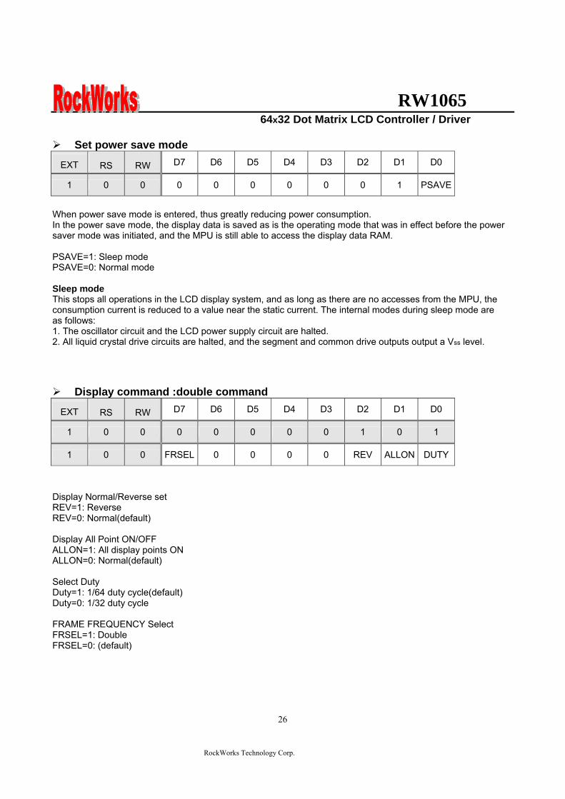
RW1065 64x32 Dot Matrix LCD Controller Driver
RockWorks Technology Corp
26
Set power save mode
EXT RS RW D7 D6 D5 D4 D3 D2 D1 D0
1 0 0 0 0 0 0 0 0 1 PSAVE
When power save mode is entered thus greatly reducing power consumption In the power save mode the display data is saved as is the operating mode that was in effect before the power saver mode was initiated and the MPU is still able to access the display data RAM PSAVE=1 Sleep mode PSAVE=0 Normal mode Sleep mode This stops all operations in the LCD display system and as long as there are no accesses from the MPU the consumption current is reduced to a value near the static current The internal modes during sleep mode are as follows 1 The oscillator circuit and the LCD power supply circuit are halted 2 All liquid crystal drive circuits are halted and the segment and common drive outputs output a Vss level
Display command double command
EXT RS RW D7 D6 D5 D4 D3 D2 D1 D0
1 0 0 0 0 0 0 0 1 0 1
1 0 0 FRSEL 0 0 0 0 REV ALLON DUTY
Display NormalReverse set REV=1 Reverse REV=0 Normal(default) Display All Point ONOFF ALLON=1 All display points ON ALLON=0 Normal(default) Select Duty Duty=1 164 duty cycle(default) Duty=0 132 duty cycle FRAME FREQUENCY Select FRSEL=1 Double FRSEL=0 (default)
RW1065 64x32 Dot Matrix LCD Controller Driver
RockWorks Technology Corp
27
Hardware Pin Set
Select ADC by ADC Pin The pin selects the relationship between display data RAM column addresses and segment drivers ADC=1 SEG0larrcolumn address 3FHhellipinverted ADC=0 SEG0larrcolumn address 00Hhellipnormal(default) This command is provided to reduce restrictions on the placement of driver ICs and routing of traces during printed circuit Board design See Figure 4 for a table of segments and column addresses for the two values of D
Select SHL by SHL Pin The pin selects the com output scan direction SHL=1 Reverse directioncom63rarrcom0 SHL=0 Normal com0rarrcom63 Both master and slave should set identical SHL value
Select LCD Bias by BS0 BS1 Pin
BS1 BS0 Bias 0 0 15 bias 0 1 16 bias 1 0 18 bias 1 1 19 bias
RW1065 64x32 Dot Matrix LCD Controller Driver
RockWorks Technology Corp
28
When an External Resistance is Used The liquid crystal power supply voltage V0 is set by adding resistors Rarsquo and Rbrsquo between VDD and VR and between VR and V0 respectively
RW1065
RW1065 64x32 Dot Matrix LCD Controller Driver
RockWorks Technology Corp
29
The set voltage circuits
Using the step-up voltage circuits equipped within the RW1065 chips it is possible to produce a 2X 3X 4X step-up voltage levels 2X step-up
To produce voltage level in the positive direction at the Vout terminal that is 2 times the voltage difference between VSS and VDD2 Please configure set voltage circuits like this Place a 1uF~22uF capacitor between CAP1N and CAP1P Place a 1uF~22uF capacitor between VSS and VOUT Short CAP2P CAP3P and VOUT Leave CAP2N open 3X step-up
To produce voltage level in the positive direction at the Vout terminal that is 3 times the voltage difference between VSS and VDD2 Please configure set voltage circuits like this Place a 1uF~22uF capacitor between CAP1N and CAP1P Place a 1uF~22uF capacitor between VSS and VOUT Place a 1uF~22uF capacitor and 100 ohms resistor between CAP2N and CAP2P Short CAP3P and Vout 4X step-up
To produce voltage level in the positive direction at the Vout terminal that is 4 times the voltage difference between VSS and VDD2 Please configure set voltage circuits like this Place a 1uF~22uF capacitor between CAP1N and CAP1P Place a 1uF~22uF capacitor between VSS and VOUT Place a 1uF~22uF capacitor and 100 ohms resistor between CAP2N and CAP2P Place a 1uF~22uF capacitor and 100 ohms resistor between CAP1N and CAP3P
RW1065 64x32 Dot Matrix LCD Controller Driver
RockWorks Technology Corp
30
ABSOLUTE MAXIMUM RATINGS Characteristics Symbol Value Unit
Power supply voltage VDD -03 to +70 V
LCD driver voltage Vout 0 to +17 V
Input voltage VIN -03 to VDD+03 V
Operating temperature TA -40 to +85
Storage temperature TSTO -55 to +125
DC CHARACTERISTICS
Rating Item Symbol Condition Min Typ Max Unit ApplicablePin
Operating Voltage VDD - 27 30 55 V VDD1
Step up output voltage Vout (Relative to VDD) 0 - 17 V Vout
Voltage follower circuit operating Voltage V0 (Relative to VDD) 0 - 15 V V0
V0 accuracy V0 - 0 - 15 V0
High-level Input Voltage Low-level Input Voltage
VIHC VILC - 07 VDD
Vss - VDD 09 V 2
High-level Output Voltage Low-level Output Voltage
VOHC VOLC
IOH = ndash05 mA IOL = 05 mA
08VDD Vss - VDD
02 VDD V 3
Input leakage current ILI VIN = VDD or VSS -1 - 2 uA 4
Output leakage current ILO - -1 1 uA 5
Liquid Crystal Driver ON Resistance RON
Ta= 25degC(Relative To VDD)
V0 =15 V - 16 20 KΩ SEGn COMn 6
Internal Oscillator fOSC 2286 254 2794 Oscillator
Frequency External Input RECOMMAND fCL
Ta = 25degC 132Duty 2286 254 2794
kHz CL
Internal Oscillator fOSC 45 5 55 Oscillator
Frequency External Input RECOMMAND fCL
Ta = 25degC 164Duty 45 5 55
kHz CL
bullDynamic Consumption Current During Display with the Internal Power Supply OFF Current consumed by total ICs when an external power supply is used
Unless otherwise specified Vss=0V VDD=30V
RW1065 64x32 Dot Matrix LCD Controller Driver
RockWorks Technology Corp
31
Display Pattern OFF
Ta = 25degC Vout=17V Rating Item Symbol Condition Min Typ Max Unit Notes
VDD=30 V V0-Vss=8V - 10 15 RW1065 IDD VDD=50 V V0-Vss=8V - 35 45
microA 7
Display Pattern Checker
Ta = 25degC Vout=17V Rating Item Symbol Condition Min Typ Max Unit Notes
VDD=30 V V0-Vss=8V - 15 20 RW1065 IDD VDD=50 V V0-Vss=8V - 40 50
microA 7
Display Pattern OFF
Ta = 25degC Vout=17V Rating Item Symbol Condition Min Typ Max Unit Notes
VDD=30 V V0-Vss=8V - 15 20 RW1065 IDD VDD=50 V V0-Vss=8V - 40 50
microA 7
Display pattern Checker
Ta = 25degC Vout=17V Rating Item Symbol Condition Min Typ Max Unit Notes
VDD=30 V V0-Vss=8V - 65 80 RW1065 IDD VDD=50 V V0-Vss=8V - 130 150
microA 7
bull Consumption Current at Time of Power Saver Mode VSS = 0 V VDD = 30 V plusmn 10
Rating Item Symbol Condition Min Typ Max Unit Notes
Sleep mode IDD - - 5 10 microA -
References for items market with 1 While a broad range of operating voltages is guaranteed performance cannot be guaranteed if there are sudden fluctuations to the
voltage while the MPU is being accessed 2 The RS D0 to D5 D6 D7 E RW CS1BP CS2P CLS CL FR MS and RST
― terminals
3 The D0 to D7 FR and CL terminals 4 The RS E RW CS1BP CS2P CLS MS and RST
― terminals
5 Applies when the D0 to D5 D6 D7 CL and FR terminals are in a high impedance state 6 These are the resistance values for when a 01 V voltage is applied between the output terminals SEGn or COMn and
the various power supply terminals (V1 V2 V3 and V4) These are specified for the operating voltage (3) range RON = 01 V ∆I (Where ∆I is the current that flows when 01 V is applied while the power supply is ON)
7 It indicates the current consumed on ICs alone when the internal oscillator circuit and display are turned on Does not include the current due to the LCD panel capacity and wiring capacity Applicable only when there is no access from the MPU
RW1065 64x32 Dot Matrix LCD Controller Driver
RockWorks Technology Corp
32
TIMING CHARACTERISTICS
68 Interface
(Ta=-40 to 85 degC) VDD=27 to 45V
Rating VDD=45 to 55V
Rating Item Signal Symbol ConditionMin Max Min Max
Units
Address hold time RS tAH6 0 mdash 0 mdash Address setup time RS tAW6
mdash 0 mdash 0 mdash
ns
System cycle time RS tCYC6 mdash 900 mdash 800 mdash ns Data setup time D0 to D7 tDS6 100 mdash 100 mdash Data hold time D0 to D7 tDH6
mdash 0 mdash 0 mdash
ns
Access time D0 to D7 tACC6 mdash 350 mdash 250
Output disable time D0 to D7 tOH6 CL = 100 pF
mdash 300 mdash 200 ns
Read tEWHR 360 mdash 300 mdash Enable H pulse time
WriteE
tEWHW mdash
360 mdash 300 mdash ns
Read tEWLR 450 mdash 400 mdash Enable L pulse time
WriteE
tEWLW mdash
450 mdash 400 mdash ns
1 All timing is specified using 20 and 80 of VDD as the reference 2 tEWLW and tEWLR are specified as the overlap between CS1BP being ldquoLrdquo (CS2P = ldquoHrdquo) and E
RW1065 64x32 Dot Matrix LCD Controller Driver
RockWorks Technology Corp
33
Reset Timing
Rating Item Signal Symbol Condition
Min Typ Max Units
Reset time mdash tR mdash mdash - 2 micros
Reset ldquoLrdquo pulse width RST tRW mdash 2 - mdash micros
1 When double chip was be used then the duty set command must be set between the tR
RW1065 64x32 Dot Matrix LCD Controller Driver
RockWorks Technology Corp
34
IO PAD CONFIGURATION
RW1065 64x32 Dot Matrix LCD Controller Driver
RockWorks Technology Corp
35
THE MPU INTERFACE (REFERENCE EXAMPLES) The RW1065 Series can be connected to 6800 Series MPUs The display area can be enlarged by using multiple RW1065 Series chips When this is done the chip select signal can be used to select the individual ICs to access
6800 Series MPUs
RW
106
5
RW1065 64x32 Dot Matrix LCD Controller Driver
RockWorks Technology Corp
36
When using external multi-level power supply for LCD driving (REFERENCE EXAMPLE)
Using a resistor divider can provide RW1065 external multi-level power supply for LCD driving
The circuit below shows a resistor divider network which can bias V0 V1 V2 V3 and V4 externally
RW1065 64x32 Dot Matrix LCD Controller Driver
RockWorks Technology Corp
37
bullWhen V0 V1 V2 V3 and V4 are biased by external power supply analog section of RW1065 should be turn off by software during LCD initialization The example in below shows the sequence to turn off analog section when external bias is used Begin of LCD initialization 1 Reset RW1065 2 SET EXT=1 (mode instruction)
RS RW DB7 DB6 DB5 DB4 DB3 DB2 DB1 DB00 0 0 0 0 0 1 1 0 1
3 SET Display Command (double command)
RS RW DB7 DB6 DB5 DB4 DB3 DB2 DB1 DB00 0 0 0 0 0 0 1 0 1 0 0 0 0 1 1 0 0 0 1
4 SET EXT=1 (mode instruction)
RS RW DB7 DB6 DB5 DB4 DB3 DB2 DB1 DB00 0 0 0 0 0 1 1 0 0
End of LCD initialization
bullBecause pins can not set LCD bias when external power supplies are used for LCD driving the bias can be set by an appropriate configuration for a resistor voltage divider networks The example is shown below
VSS
R
R
NR
R
R
RV1
RV2
RV3
RV4
V0
Bias Network Circuit Concept 15 Bias N=1 total = 5R 16 Bias N=2 total =6R 18 Bias N=4 total =8R 19 Bias N=5 total = 9R
RW1065 64x32 Dot Matrix LCD Controller Driver
RockWorks Technology Corp
38
Single chip solution for RW1065 application (REFERENCE EXAMPLE)
For a 64x32 application the duty cycle of LCD panel is 164 and the display duty of RW1065 should be set to 164 The display duty cycle can be selected by the DUTY bit in display command The diagram for 64x32 application is shown below
64 SEGx32COM LCD Panel
164 duty cycle
RW1065 DUTY=1
COM1~33
SEG1~65
RW1065 64x32 Dot Matrix LCD Controller Driver
RockWorks Technology Corp
39
Using an adjustable resistor on the main board to adjust the contrast of liquid crystal display (REFERENCE EXAMPLE)
The schematic shows an adjustable resistor on main board that can adjust voltage level of V0
RW1065 64x32 Dot Matrix LCD Controller Driver
RockWorks Technology Corp
40
Package information (Please pay close attention to the information in this section Do not hesitate to consult with our sale representative if you have any question or concern)
In order to make better bonding yield for RW1065 please follow the tips and recommendations in this section In this section few tips about COB footprint style PCB layout and wire bonding will be discussed
The drawing in below shows the PCB footprint style which we recommend for RW1065 Pads array in
curve shape is easier for Al wire bonding Besides that a real size COB footprint for RW1065 is also shown in below RW1065 COB footprint is also available in powerpcb or protel format for design reference purpose
The ratio is 11
RW1065 64x32 Dot Matrix LCD Controller Driver
RockWorks Technology Corp
41
During COB footprint design there have some tips about footprint that the PCB designer should know The angle between bonding wire and vertical line should less than 45 Otherwise the wire shorts would become very easy to happen at fours corners of the chip
The angle between bonding wire and vertical line could be reduced by expanding the distance between pads array and the chip In addition reducing length in horizon direction of pads array could minimize the angle between bonding wire and vertical line The picture in below will help to illustrate this concept From the experiences COB footprint style affects the bonding yield
Bad Wires are too close to each other
The angle between bonding wire and vertical line is greater than 45
The angle between bonding wire and vertical line is less than 45
Wires are not too close to each other
Reducing length in horizon direction of pads array could minimize the angle between bonding wire and vertical line
The angle between bonding wire and vertical line could be reduced by expanding the distance between pads array and the chip
RW1065 64x32 Dot Matrix LCD Controller Driver
RockWorks Technology Corp
42
If the gap between pads of COB footprint is filled with solder mask coating it is difficult to bond Al wire to
the pads The top solder masks layer that overlap COB footprint area should be removed
Please use 1 mils diameter Al wire for RW1065 wire bonding
1 2 3 4 5 6
A
B
C
D
654321
D
C
B
A
Title
Number RevisionSize
C
Date 29-Aug-2007 Sheet of File D公司資料99seMyDesignddb Drawn By
RW1065
COM131
COM142
COM153
COM164
COM175
COM186
COM197
COM208
COM219
COM2210
COM2311
COM2412
COM2513
COM2614
COM2715
COM2816
COM2917
COM3018
COM3119
SEG
6320
SEG
6221
SEG
6122
SEG
6023
SEG
5924
SEG
5825
SEG
5726
SEG
5627
SEG
5528
SEG
5429
SEG
5330
SEG
5231
SEG
5132
SEG
5033
SEG
4934
SEG
4835
SEG
4736
SEG
4637
SEG
4538
SEG
4439
SEG
4340
SEG
4241
SEG
4142
SEG
4043
SEG
3944
SEG
3845
SEG
3746
SEG
3647
SEG
3548
SEG
3449
SEG
3350
SEG
3251
SEG
3152
SEG
3053
SEG
2954
SEG
2855
SEG
2756
SEG
2657
SEG
2558
SEG
2459
SEG
2360
SEG
2261
SEG
2162
SEG
2063
SEG
1964
SEG
1865
SEG
1766
SEG
1667
SEG
1568
SEG
1469
SEG13 70SEG12 71SEG11 72SEG10 73SEG9 74SEG8 75SEG7 76SEG6 77SEG5 78SEG4 79SEG3 80SEG2 81SEG1 82SEG0 83ADCP 84CLL 85
VSS
86D
087
D1
88D
289
D3
90D
491
D5
92D
693
D7
94C
S1B
P95
CS2
P96
ERD
P97
AO
P(R
S)98
RW
RP
99V
DD
100
RST
P10
1C
LSP
102
FRR
103
MSP
104
BS1
P10
5B
S0P
106
SHLP
107
VD
D2
108
CA
P2N
109
CA
P2P
110
CA
P1P
111
CA
P1N
112
CA
P3P
113
VO
UT
114
V0
115
VR
AB
116
V3
117
V2
118
V4
119
V1
120
CO
M0
121
CO
M1
122
CO
M2
123
CO
M3
124
CO
M4
125
CO
M5
126
CO
M6
127
CO
M7
128
CO
M8
129
CO
M9
130
CO
M10
131
CO
M11
132
CO
M12
133
4897x1902 um
IC1
RW1065
C9CAPR4
100R0603
R30R0603
C8
CAP
C7
CAP
R2
100R0603
R1
0R0603C6 22uf
R50R
R6300R
R7RES1
R8NC R9
100R0603
VDD
R10
NC
R11
100R0603
R12
100R0603
R13
NC
R14
100R0603
R15
NC
VDD
D0
D1
D2
D3
D4
D5
D6
D7
DB[07]
VDDC5
01uf0603
VD
D
CS2
P
123456789
1011121314151617181920
J1
CON20
C1201uf0603
R3951K0603
VDD
CAP Value1UF~22UF
2XPut C6C8 Short R1R3Open R2R4C7C93XPut C6C8C9 R4Short R1Open R2R3C74XOpen R1R3
BS0 BS1 Bias0 0
0 1
1 0
11
15 bias
16 bias
18 bias
19 bias
ADC=0 SEG0lt~column address 00Hnormal(default) ADC=1 SEG0lt~column address 3FHinverted
SHL=0 Normal COM0~gtCOM63(default)SHL=1 Reverse direction COM63~gtCOM0
R16100R0603
LCD PANEL 64X32RockWorks
RW1065 64X32
COM0-31 SEG0-63SHL=0 ADC=0
SHL=1COM31-0
ADC=1SEG63-0
if use single chip for 32 command displaythe display command must select 164 dutyDisplay panel must select 164 duty type
VO
UT
C3P
C1N
C1P
C2P
C2N
VDD2
ADC
SHL
BS0
BS1
CLLADC
V1
V2
V3
V4
VR
AB
V0
VO
UT
C3P
C1N
C1P
C2P
C2N
VD
D2
SHL
BS0
BS1
FRR
RST
P
RW
RS
E CS1
B
CS1
V0RSRWED0D1D2D3D4D5D6D7
RSTPAK
C4
22uf
RBRES1
RA1RES1
C2
22uf
C1
22uf
C3
22uf
C0
22uf
R20
100k0603
R21
100k0603
R17
200K0603
V1
V2
V3
V4 VRAB
V0
V0
OPTION
B
R18
300R0603
RA2RES1
VADJ
R19100R
R23 RES1R22 0R
R24
RES1
R25
0R
VDD
CS1BP
CS2P
CS1
CS1
R26
22R0603
R27
22R0603
C1047uf
C11
01uf
VSS_INVDD_IN
D1DIODE
FGND
鐵框地
VSS
VDD
R28 10RR29 10RR30 10RR31 10RR32 10RR33 10RR34 10RR35 10RR36 10RR37 10RR38 10R
VADJ
1 2 3 4 5 6
A
B
C
D
654321
D
C
B
A
Title
Number RevisionSize
C
Date 29-Aug-2007 Sheet of File D公司資料99seMyDesignddb Drawn By
RW1065
COM131
COM142
COM153
COM164
COM175
COM186
COM197
COM208
COM219
COM2210
COM2311
COM2412
COM2513
COM2614
COM2715
COM2816
COM2917
COM3018
COM3119
SEG
6320
SEG
6221
SEG
6122
SEG
6023
SEG
5924
SEG
5825
SEG
5726
SEG
5627
SEG
5528
SEG
5429
SEG
5330
SEG
5231
SEG
5132
SEG
5033
SEG
4934
SEG
4835
SEG
4736
SEG
4637
SEG
4538
SEG
4439
SEG
4340
SEG
4241
SEG
4142
SEG
4043
SEG
3944
SEG
3845
SEG
3746
SEG
3647
SEG
3548
SEG
3449
SEG
3350
SEG
3251
SEG
3152
SEG
3053
SEG
2954
SEG
2855
SEG
2756
SEG
2657
SEG
2558
SEG
2459
SEG
2360
SEG
2261
SEG
2162
SEG
2063
SEG
1964
SEG
1865
SEG
1766
SEG
1667
SEG
1568
SEG
1469
SEG13 70SEG12 71SEG11 72SEG10 73SEG9 74SEG8 75SEG7 76SEG6 77SEG5 78SEG4 79SEG3 80SEG2 81SEG1 82SEG0 83ADCP 84CLL 85
VSS
86D
087
D1
88D
289
D3
90D
491
D5
92D
693
D7
94C
S1B
P95
CS2
P96
ERD
P97
AO
P(R
S)98
RW
RP
99V
DD
100
RST
P10
1C
LSP
102
FRR
103
MSP
104
BS1
P10
5B
S0P
106
SHLP
107
VD
D2
108
CA
P2N
109
CA
P2P
110
CA
P1P
111
CA
P1N
112
CA
P3P
113
VO
UT
114
V0
115
VR
AB
116
V3
117
V2
118
V4
119
V1
120
CO
M0
121
CO
M1
122
CO
M2
123
CO
M3
124
CO
M4
125
CO
M5
126
CO
M6
127
CO
M7
128
CO
M8
129
CO
M9
130
CO
M10
131
CO
M11
132
CO
M12
133
4897x1902 um
IC1
RW1065 Master
RW1065
COM131
COM142
COM153
COM164
COM175
COM186
COM197
COM208
COM219
COM2210
COM2311
COM2412
COM2513
COM2614
COM2715
COM2816
COM2917
COM3018
COM3119
SEG
6320
SEG
6221
SEG
6122
SEG
6023
SEG
5924
SEG
5825
SEG
5726
SEG
5627
SEG
5528
SEG
5429
SEG
5330
SEG
5231
SEG
5132
SEG
5033
SEG
4934
SEG
4835
SEG
4736
SEG
4637
SEG
4538
SEG
4439
SEG
4340
SEG
4241
SEG
4142
SEG
4043
SEG
3944
SEG
3845
SEG
3746
SEG
3647
SEG
3548
SEG
3449
SEG
3350
SEG
3251
SEG
3152
SEG
3053
SEG
2954
SEG
2855
SEG
2756
SEG
2657
SEG
2558
SEG
2459
SEG
2360
SEG
2261
SEG
2162
SEG
2063
SEG
1964
SEG
1865
SEG
1766
SEG
1667
SEG
1568
SEG
1469
SEG13 70SEG12 71SEG11 72SEG10 73SEG9 74SEG8 75SEG7 76SEG6 77SEG5 78SEG4 79SEG3 80SEG2 81SEG1 82SEG0 83ADCP 84CLL 85
VSS
86D
087
D1
88D
289
D3
90D
491
D5
92D
693
D7
94C
S1B
P95
CS2
P96
ERD
P97
AO
P(R
S)98
RW
RP
99V
DD
100
RST
P10
1C
LSP
102
FRR
103
MSP
104
BS1
P10
5B
S0P
106
SHLP
107
VD
D2
108
CA
P2N
109
CA
P2P
110
CA
P1P
111
CA
P1N
112
CA
P3P
113
VO
UT
114
V0
115
VR
AB
116
V3
117
V2
118
V4
119
V1
120
CO
M0
121
CO
M1
122
CO
M2
123
CO
M3
124
CO
M4
125
CO
M5
126
CO
M6
127
CO
M7
128
CO
M8
129
CO
M9
130
CO
M10
131
CO
M11
132
CO
M12
133
4897x1902 um
IC2
RW1065 Slave
C4
22uf
RBRES1
RA1RES1
C2
22uf
C1
22uf
C3
22uf
C0
22ufC9CAPR4
100R0603
R30R0603
C8
CAP
C7
CAP
R2
100R0603
R1
0R0603C6 22uf
R50R0603
R6300R0603
R7RES1
R8NC R9
100R0603
VDD
R10
NC
R11
100R0603
R12
NC
R13
100R0603
R14
100R0603
R15
NC
R16
100R0603
R17
NC
VDD
D0
D1
D2
D3
D4
D5
D6
D7
D0
D1
D2
D3
D4
D5
D6
D7
DB[07] DB[07]
VDDC10
01uf0603
VD
D
IC1_
CS2
P
VDD
IC2_
CS2
P
VD
D
C11
01uf0603
VSS
VSS
LCD PANEL 128X64
Master COM0-31 Slave COM32-63
Master SEG0-63 Slave SEG64-127
123456789
1011121314151617181920
J1
CON20
Master Slave
CAP Value1UF~22UF
2XPut C6C8 Short R1R3Open R2R4C7C93XPut C6C8C9 R4Short R1Open R2R3C74XOpen R1R3
RockWorksRW1065 128x64
BS0 BS1 Bias0 0
0 1
1 0
11
15 bias
16 bias
18 bias
19 bias
ADC=0 SEG0lt~column address 00Hnormal(default) ADC=1 SEG0lt~column address 3FHinverted
SHL=0 Normal COM0~gtCOM63(default)SHL=1 Reverse direction COM63~gtCOM0Both Master and Slave should set identical SHL value
SHL=0 SHL=0
ADC=0 ADC=0
Slave COM31-0
Slave SEG127-64
SHL=1
ADC=1
SHL=1Master COM63-32
ADC=1Master SEG63-0
R18100R0603
R22
100k0603
R23
100k0603
C501uF0603
R4551K0603
VDD
R19
200K0603
ADC1
ADC2
SHL
BS0
BS1
VDD2
V1
V2
V3
V4 VRAB
V0
V0V
OU
T
C3P
C1N
C1P
C2P
C2N
V1
V2
V3
V4
VR
AB
V0
VO
UT
C3P
C1N
C1P
C2P
C2N
VD
D2
SHL
BS0
BS1
FRR
RST
P
RW
RS
E IC1_
CS1
BP
V1
V2
V3
V4
VR
AB
V0
VO
UT
VD
D2
SHL
BS0
BS1
FRR
RST
P
RW
RS
E IC2_
CS1
BP
CLLADC1
CLLADC2
RSTP
CS1CS2
V0RSRWED0D1D2D3D4D5D6D7
AK
OPTION
R20
300R0603
RA2RES1
VADJ
R21
100R
B
R25 RESR24 0R
R26 RES R27 0RVDD
IC1_CS1BP
IC1_CS2P
CS1
CS1
R28 0R R29 RES
R30 RES R31 0R
IC2_CS1BP
IC2_CS2P
CS2
CS2
R32
22R0603
R33
22R0603
C1001uf
C11
47uf
D1DIODE
FGND
鐵框地
VSS
VDD
R34 10RR35 10RR36 10RR37 10RR38 10RR39 10RR40 10RR41 10RR42 10RR43 10RR44 10R
VSS_INVDD_IN
VADJ
VDD
1 2 3 4 5 6 7 8
A
B
C
D
87654321
D
C
B
A
Title
Number RevisionSize
D
Date 29-Aug-2007 Sheet of File D公司資料 99seMyDesignddb Drawn By
C422uf
RBRES1
RA1RES1
C3
22uf
C2
22uf
C1
22uf
C0
22ufC9CAPR4
100R0603
R30R0603
C8
CAP
C7
CAP
R2
100R0603
R1
0R0603C6 22uf
R220R0603
R23300R0603
R24RES1
R39
NCR40
100 ohm0603
VDD
R41
NC
R42
100 ohm0603
R43
NC
R44
100 ohm0603
R45
NC
R46
100 ohm0603
R47
100 ohm0603
R48
NC
R49
100 ohm0603
R50
NC
VDDCAP Value1UF~22UF
2XPut C6C8 Short R1R3Open R2R4C7C93XPut C6C8C9 R4Short R1Open R2R3C74XOpen R1R3
BS0 BS1 Bias0 0
0 1
1 0
11
15 bias
16 bias
18 bias
19 bias
ADC=0 SEG0lt~column address 00Hnormal(default)
ADC=1 SEG0lt~column address 3FHinverted
SHL=0 Normal COM0~gtCOM63(default)SHL=1 Reverse direction COM63~gtCOM0Both Master and Slave should set identical SHL value
R7
100k0603
R8
100k0603
V1
V2
V3
V4
V0
VRAB
V0
R5
200K
VDD2
VO
UT
C3P
C1N
C1P
C2P
C2N
ADC1
ADC2
ADC3
SHL
BS0
BS1
CS1CS2CS3
V0RSRWED0D1D2D3D4D5D6D7
RSTP
R3851K0603
C5
01uF
VDD
OPTION
R6
300R0603R9100R
RA2RES1
VADJ
RW1065
COM131
COM142
COM153
COM164
COM175
COM186
COM197
COM208
COM219
COM2210
COM2311
COM2412
COM2513
COM2614
COM2715
COM2816
COM2917
COM3018
COM3119
SEG
6320
SEG
6221
SEG
6122
SEG
6023
SEG
5924
SEG
5825
SEG
5726
SEG
5627
SEG
5528
SEG
5429
SEG
5330
SEG
5231
SEG
5132
SEG
5033
SEG
4934
SEG
4835
SEG
4736
SEG
4637
SEG
4538
SEG
4439
SEG
4340
SEG
4241
SEG
4142
SEG
4043
SEG
3944
SEG
3845
SEG
3746
SEG
3647
SEG
3548
SEG
3449
SEG
3350
SEG
3251
SEG
3152
SEG
3053
SEG
2954
SEG
2855
SEG
2756
SEG
2657
SEG
2558
SEG
2459
SEG
2360
SEG
2261
SEG
2162
SEG
2063
SEG
1964
SEG
1865
SEG
1766
SEG
1667
SEG
1568
SEG
1469
SEG13 70SEG12 71SEG11 72SEG10 73SEG9 74SEG8 75SEG7 76SEG6 77SEG5 78SEG4 79SEG3 80SEG2 81SEG1 82SEG0 83ADCP 84CLL 85
VSS
86D
087
D1
88D
289
D3
90D
491
D5
92D
693
D7
94C
S1B
P95
CS2
P96
ERD
P97
AO
P(R
S)98
RW
RP
99V
DD
100
RST
P10
1C
LSP
102
FRR
103
MSP
104
BS1
P10
5B
S0P
106
SHLP
107
VD
D2
108
CA
P2N
109
CA
P2P
110
CA
P1P
111
CA
P1N
112
CA
P3P
113
VO
UT
114
V0
115
VR
AB
116
V3
117
V2
118
V4
119
V1
120
CO
M0
121
CO
M1
122
CO
M2
123
CO
M3
124
CO
M4
125
CO
M5
126
CO
M6
127
CO
M7
128
CO
M8
129
CO
M9
130
CO
M10
131
CO
M11
132
CO
M12
133
4897x1902 um
IC1
RW1065 Master
RW1065
COM131
COM142
COM153
COM164
COM175
COM186
COM197
COM208
COM219
COM2210
COM2311
COM2412
COM2513
COM2614
COM2715
COM2816
COM2917
COM3018
COM3119
SEG
6320
SEG
6221
SEG
6122
SEG
6023
SEG
5924
SEG
5825
SEG
5726
SEG
5627
SEG
5528
SEG
5429
SEG
5330
SEG
5231
SEG
5132
SEG
5033
SEG
4934
SEG
4835
SEG
4736
SEG
4637
SEG
4538
SEG
4439
SEG
4340
SEG
4241
SEG
4142
SEG
4043
SEG
3944
SEG
3845
SEG
3746
SEG
3647
SEG
3548
SEG
3449
SEG
3350
SEG
3251
SEG
3152
SEG
3053
SEG
2954
SEG
2855
SEG
2756
SEG
2657
SEG
2558
SEG
2459
SEG
2360
SEG
2261
SEG
2162
SEG
2063
SEG
1964
SEG
1865
SEG
1766
SEG
1667
SEG
1568
SEG
1469
SEG13 70SEG12 71SEG11 72SEG10 73SEG9 74SEG8 75SEG7 76SEG6 77SEG5 78SEG4 79SEG3 80SEG2 81SEG1 82SEG0 83ADCP 84CLL 85
VSS
86D
087
D1
88D
289
D3
90D
491
D5
92D
693
D7
94C
S1B
P95
CS2
P96
ERD
P97
AO
P(R
S)98
RW
RP
99V
DD
100
RST
P10
1C
LSP
102
FRR
103
MSP
104
BS1
P10
5B
S0P
106
SHLP
107
VD
D2
108
CA
P2N
109
CA
P2P
110
CA
P1P
111
CA
P1N
112
CA
P3P
113
VO
UT
114
V0
115
VR
AB
116
V3
117
V2
118
V4
119
V1
120
CO
M0
121
CO
M1
122
CO
M2
123
CO
M3
124
CO
M4
125
CO
M5
126
CO
M6
127
CO
M7
128
CO
M8
129
CO
M9
130
CO
M10
131
CO
M11
132
CO
M12
133
4897x1902 um
IC2
RW1065 Slave
D0
D1
D2
D3
D4
D5
D6
D7
D0
D1
D2
D3
D4
D5
D6
D7
DB[07] DB[07]
VDDC8
01uf0603
VD
D
VDD
VD
D
C9
01uf0603
VSS
VSS
LCD PANEL 192X64
Master COM0-31 Slave COM32-63
Master SEG0-63 Slave SEG64-127
Master Slave
RockWorksRW1065 192x64
RW1065
COM131
COM142
COM153
COM164
COM175
COM186
COM197
COM208
COM219
COM2210
COM2311
COM2412
COM2513
COM2614
COM2715
COM2816
COM2917
COM3018
COM3119
SEG
6320
SEG
6221
SEG
6122
SEG
6023
SEG
5924
SEG
5825
SEG
5726
SEG
5627
SEG
5528
SEG
5429
SEG
5330
SEG
5231
SEG
5132
SEG
5033
SEG
4934
SEG
4835
SEG
4736
SEG
4637
SEG
4538
SEG
4439
SEG
4340
SEG
4241
SEG
4142
SEG
4043
SEG
3944
SEG
3845
SEG
3746
SEG
3647
SEG
3548
SEG
3449
SEG
3350
SEG
3251
SEG
3152
SEG
3053
SEG
2954
SEG
2855
SEG
2756
SEG
2657
SEG
2558
SEG
2459
SEG
2360
SEG
2261
SEG
2162
SEG
2063
SEG
1964
SEG
1865
SEG
1766
SEG
1667
SEG
1568
SEG
1469
SEG13 70SEG12 71SEG11 72SEG10 73SEG9 74SEG8 75SEG7 76SEG6 77SEG5 78SEG4 79SEG3 80SEG2 81SEG1 82SEG0 83ADCP 84CLL 85
VSS
86D
087
D1
88D
289
D3
90D
491
D5
92D
693
D7
94C
S1B
P95
CS2
P96
ERD
P97
AO
P(R
S)98
RW
RP
99V
DD
100
RST
P10
1C
LSP
102
FRR
103
MSP
104
BS1
P10
5B
S0P
106
SHLP
107
VD
D2
108
CA
P2N
109
CA
P2P
110
CA
P1P
111
CA
P1N
112
CA
P3P
113
VO
UT
114
V0
115
VR
AB
116
V3
117
V2
118
V4
119
V1
120
CO
M0
121
CO
M1
122
CO
M2
123
CO
M3
124
CO
M4
125
CO
M5
126
CO
M6
127
CO
M7
128
CO
M8
129
CO
M9
130
CO
M10
131
CO
M11
132
CO
M12
133
4897x1902 um
IC3
RW1065 Slave
D0
D1
D2
D3
D4
D5
D6
D7
DB[07]
VSS
VSS
VDD
VD
D
C10
01uf0603
Slave SEG128-192
Slave
SHL=0 SHL=0
Master COM63-32SHL=1 SHL=1
Slave COM31-0ADC=0 ADC=0 ADC=0
ADC=1 ADC=1 ADC=1Master SEG63-0 Slave SEG127-64 Slave SEG192-128
R50100R0603
V1
V2
V3
V4
VR
AB
V0
VO
UT
C3P
C1N
C1P
C2P
C2N
VD
D2
SHL
BS0
BS1
FRR
RST
P
RW
RS
E V1
V2
V3
V4
VR
AB
V0
VO
UT
VD
D2
SHL
BS0
BS1
FRR
RST
P
RW
RS
E V1
V2
V3
V4
VR
AB
V0
VO
UT
VD
D2
SHL
BS0
BS1
FRR
RST
P
RW
RS
E
CLL CLL CLLADC1 ADC2 ADC3
R25 10RR26 10RR27 10RR28 10RR29 10RR30 10RR31 10RR32 10RR33 10RR34 10RR35 10R
R36
22R0603
D1DIODE
R3722R0603
C647uf
C701uf
VSS_INVDD_IN
VSS
VDD
VADJ
123456789
101112131415161718192021222324
J1
CON24
AK
FGND
鐵框地
IC1_
CS1
BP
IC1_
CS2
P
IC2_
CS2
PIC
2_C
S1B
P
IC3_
CS1
BP
IC3_
CS2
B
R10 0R R11 RES
R12 RES R13 0RVDD
IC1_CS2B
IC1_CS1BPCS1
CS1
R14 0R R15 RES
R16 RES R17 0RVDDIC2_CS2B
IC2_CS1BPCS2
CS2
R18 0R R19 RES
R20 RES R21 0RVDDIC3_CS2B
IC3_CS1BPCS3
CS3
B
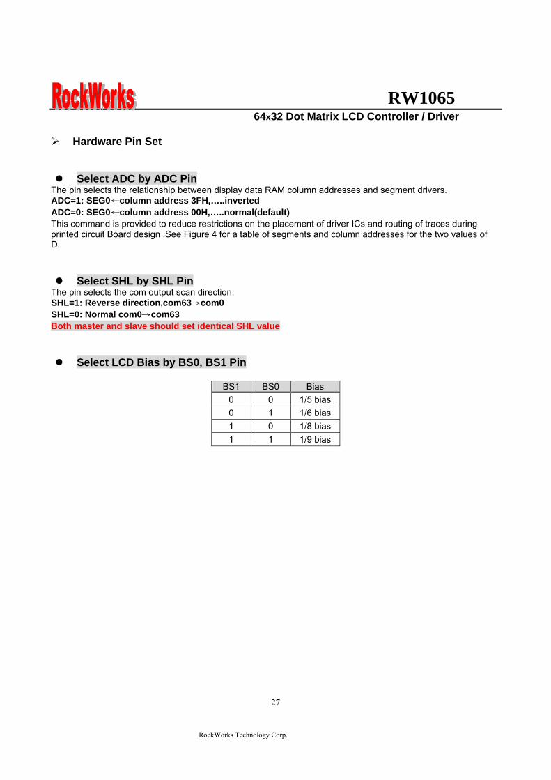
RW1065 64x32 Dot Matrix LCD Controller Driver
RockWorks Technology Corp
27
Hardware Pin Set
Select ADC by ADC Pin The pin selects the relationship between display data RAM column addresses and segment drivers ADC=1 SEG0larrcolumn address 3FHhellipinverted ADC=0 SEG0larrcolumn address 00Hhellipnormal(default) This command is provided to reduce restrictions on the placement of driver ICs and routing of traces during printed circuit Board design See Figure 4 for a table of segments and column addresses for the two values of D
Select SHL by SHL Pin The pin selects the com output scan direction SHL=1 Reverse directioncom63rarrcom0 SHL=0 Normal com0rarrcom63 Both master and slave should set identical SHL value
Select LCD Bias by BS0 BS1 Pin
BS1 BS0 Bias 0 0 15 bias 0 1 16 bias 1 0 18 bias 1 1 19 bias
RW1065 64x32 Dot Matrix LCD Controller Driver
RockWorks Technology Corp
28
When an External Resistance is Used The liquid crystal power supply voltage V0 is set by adding resistors Rarsquo and Rbrsquo between VDD and VR and between VR and V0 respectively
RW1065
RW1065 64x32 Dot Matrix LCD Controller Driver
RockWorks Technology Corp
29
The set voltage circuits
Using the step-up voltage circuits equipped within the RW1065 chips it is possible to produce a 2X 3X 4X step-up voltage levels 2X step-up
To produce voltage level in the positive direction at the Vout terminal that is 2 times the voltage difference between VSS and VDD2 Please configure set voltage circuits like this Place a 1uF~22uF capacitor between CAP1N and CAP1P Place a 1uF~22uF capacitor between VSS and VOUT Short CAP2P CAP3P and VOUT Leave CAP2N open 3X step-up
To produce voltage level in the positive direction at the Vout terminal that is 3 times the voltage difference between VSS and VDD2 Please configure set voltage circuits like this Place a 1uF~22uF capacitor between CAP1N and CAP1P Place a 1uF~22uF capacitor between VSS and VOUT Place a 1uF~22uF capacitor and 100 ohms resistor between CAP2N and CAP2P Short CAP3P and Vout 4X step-up
To produce voltage level in the positive direction at the Vout terminal that is 4 times the voltage difference between VSS and VDD2 Please configure set voltage circuits like this Place a 1uF~22uF capacitor between CAP1N and CAP1P Place a 1uF~22uF capacitor between VSS and VOUT Place a 1uF~22uF capacitor and 100 ohms resistor between CAP2N and CAP2P Place a 1uF~22uF capacitor and 100 ohms resistor between CAP1N and CAP3P
RW1065 64x32 Dot Matrix LCD Controller Driver
RockWorks Technology Corp
30
ABSOLUTE MAXIMUM RATINGS Characteristics Symbol Value Unit
Power supply voltage VDD -03 to +70 V
LCD driver voltage Vout 0 to +17 V
Input voltage VIN -03 to VDD+03 V
Operating temperature TA -40 to +85
Storage temperature TSTO -55 to +125
DC CHARACTERISTICS
Rating Item Symbol Condition Min Typ Max Unit ApplicablePin
Operating Voltage VDD - 27 30 55 V VDD1
Step up output voltage Vout (Relative to VDD) 0 - 17 V Vout
Voltage follower circuit operating Voltage V0 (Relative to VDD) 0 - 15 V V0
V0 accuracy V0 - 0 - 15 V0
High-level Input Voltage Low-level Input Voltage
VIHC VILC - 07 VDD
Vss - VDD 09 V 2
High-level Output Voltage Low-level Output Voltage
VOHC VOLC
IOH = ndash05 mA IOL = 05 mA
08VDD Vss - VDD
02 VDD V 3
Input leakage current ILI VIN = VDD or VSS -1 - 2 uA 4
Output leakage current ILO - -1 1 uA 5
Liquid Crystal Driver ON Resistance RON
Ta= 25degC(Relative To VDD)
V0 =15 V - 16 20 KΩ SEGn COMn 6
Internal Oscillator fOSC 2286 254 2794 Oscillator
Frequency External Input RECOMMAND fCL
Ta = 25degC 132Duty 2286 254 2794
kHz CL
Internal Oscillator fOSC 45 5 55 Oscillator
Frequency External Input RECOMMAND fCL
Ta = 25degC 164Duty 45 5 55
kHz CL
bullDynamic Consumption Current During Display with the Internal Power Supply OFF Current consumed by total ICs when an external power supply is used
Unless otherwise specified Vss=0V VDD=30V
RW1065 64x32 Dot Matrix LCD Controller Driver
RockWorks Technology Corp
31
Display Pattern OFF
Ta = 25degC Vout=17V Rating Item Symbol Condition Min Typ Max Unit Notes
VDD=30 V V0-Vss=8V - 10 15 RW1065 IDD VDD=50 V V0-Vss=8V - 35 45
microA 7
Display Pattern Checker
Ta = 25degC Vout=17V Rating Item Symbol Condition Min Typ Max Unit Notes
VDD=30 V V0-Vss=8V - 15 20 RW1065 IDD VDD=50 V V0-Vss=8V - 40 50
microA 7
Display Pattern OFF
Ta = 25degC Vout=17V Rating Item Symbol Condition Min Typ Max Unit Notes
VDD=30 V V0-Vss=8V - 15 20 RW1065 IDD VDD=50 V V0-Vss=8V - 40 50
microA 7
Display pattern Checker
Ta = 25degC Vout=17V Rating Item Symbol Condition Min Typ Max Unit Notes
VDD=30 V V0-Vss=8V - 65 80 RW1065 IDD VDD=50 V V0-Vss=8V - 130 150
microA 7
bull Consumption Current at Time of Power Saver Mode VSS = 0 V VDD = 30 V plusmn 10
Rating Item Symbol Condition Min Typ Max Unit Notes
Sleep mode IDD - - 5 10 microA -
References for items market with 1 While a broad range of operating voltages is guaranteed performance cannot be guaranteed if there are sudden fluctuations to the
voltage while the MPU is being accessed 2 The RS D0 to D5 D6 D7 E RW CS1BP CS2P CLS CL FR MS and RST
― terminals
3 The D0 to D7 FR and CL terminals 4 The RS E RW CS1BP CS2P CLS MS and RST
― terminals
5 Applies when the D0 to D5 D6 D7 CL and FR terminals are in a high impedance state 6 These are the resistance values for when a 01 V voltage is applied between the output terminals SEGn or COMn and
the various power supply terminals (V1 V2 V3 and V4) These are specified for the operating voltage (3) range RON = 01 V ∆I (Where ∆I is the current that flows when 01 V is applied while the power supply is ON)
7 It indicates the current consumed on ICs alone when the internal oscillator circuit and display are turned on Does not include the current due to the LCD panel capacity and wiring capacity Applicable only when there is no access from the MPU
RW1065 64x32 Dot Matrix LCD Controller Driver
RockWorks Technology Corp
32
TIMING CHARACTERISTICS
68 Interface
(Ta=-40 to 85 degC) VDD=27 to 45V
Rating VDD=45 to 55V
Rating Item Signal Symbol ConditionMin Max Min Max
Units
Address hold time RS tAH6 0 mdash 0 mdash Address setup time RS tAW6
mdash 0 mdash 0 mdash
ns
System cycle time RS tCYC6 mdash 900 mdash 800 mdash ns Data setup time D0 to D7 tDS6 100 mdash 100 mdash Data hold time D0 to D7 tDH6
mdash 0 mdash 0 mdash
ns
Access time D0 to D7 tACC6 mdash 350 mdash 250
Output disable time D0 to D7 tOH6 CL = 100 pF
mdash 300 mdash 200 ns
Read tEWHR 360 mdash 300 mdash Enable H pulse time
WriteE
tEWHW mdash
360 mdash 300 mdash ns
Read tEWLR 450 mdash 400 mdash Enable L pulse time
WriteE
tEWLW mdash
450 mdash 400 mdash ns
1 All timing is specified using 20 and 80 of VDD as the reference 2 tEWLW and tEWLR are specified as the overlap between CS1BP being ldquoLrdquo (CS2P = ldquoHrdquo) and E
RW1065 64x32 Dot Matrix LCD Controller Driver
RockWorks Technology Corp
33
Reset Timing
Rating Item Signal Symbol Condition
Min Typ Max Units
Reset time mdash tR mdash mdash - 2 micros
Reset ldquoLrdquo pulse width RST tRW mdash 2 - mdash micros
1 When double chip was be used then the duty set command must be set between the tR
RW1065 64x32 Dot Matrix LCD Controller Driver
RockWorks Technology Corp
34
IO PAD CONFIGURATION
RW1065 64x32 Dot Matrix LCD Controller Driver
RockWorks Technology Corp
35
THE MPU INTERFACE (REFERENCE EXAMPLES) The RW1065 Series can be connected to 6800 Series MPUs The display area can be enlarged by using multiple RW1065 Series chips When this is done the chip select signal can be used to select the individual ICs to access
6800 Series MPUs
RW
106
5
RW1065 64x32 Dot Matrix LCD Controller Driver
RockWorks Technology Corp
36
When using external multi-level power supply for LCD driving (REFERENCE EXAMPLE)
Using a resistor divider can provide RW1065 external multi-level power supply for LCD driving
The circuit below shows a resistor divider network which can bias V0 V1 V2 V3 and V4 externally
RW1065 64x32 Dot Matrix LCD Controller Driver
RockWorks Technology Corp
37
bullWhen V0 V1 V2 V3 and V4 are biased by external power supply analog section of RW1065 should be turn off by software during LCD initialization The example in below shows the sequence to turn off analog section when external bias is used Begin of LCD initialization 1 Reset RW1065 2 SET EXT=1 (mode instruction)
RS RW DB7 DB6 DB5 DB4 DB3 DB2 DB1 DB00 0 0 0 0 0 1 1 0 1
3 SET Display Command (double command)
RS RW DB7 DB6 DB5 DB4 DB3 DB2 DB1 DB00 0 0 0 0 0 0 1 0 1 0 0 0 0 1 1 0 0 0 1
4 SET EXT=1 (mode instruction)
RS RW DB7 DB6 DB5 DB4 DB3 DB2 DB1 DB00 0 0 0 0 0 1 1 0 0
End of LCD initialization
bullBecause pins can not set LCD bias when external power supplies are used for LCD driving the bias can be set by an appropriate configuration for a resistor voltage divider networks The example is shown below
VSS
R
R
NR
R
R
RV1
RV2
RV3
RV4
V0
Bias Network Circuit Concept 15 Bias N=1 total = 5R 16 Bias N=2 total =6R 18 Bias N=4 total =8R 19 Bias N=5 total = 9R
RW1065 64x32 Dot Matrix LCD Controller Driver
RockWorks Technology Corp
38
Single chip solution for RW1065 application (REFERENCE EXAMPLE)
For a 64x32 application the duty cycle of LCD panel is 164 and the display duty of RW1065 should be set to 164 The display duty cycle can be selected by the DUTY bit in display command The diagram for 64x32 application is shown below
64 SEGx32COM LCD Panel
164 duty cycle
RW1065 DUTY=1
COM1~33
SEG1~65
RW1065 64x32 Dot Matrix LCD Controller Driver
RockWorks Technology Corp
39
Using an adjustable resistor on the main board to adjust the contrast of liquid crystal display (REFERENCE EXAMPLE)
The schematic shows an adjustable resistor on main board that can adjust voltage level of V0
RW1065 64x32 Dot Matrix LCD Controller Driver
RockWorks Technology Corp
40
Package information (Please pay close attention to the information in this section Do not hesitate to consult with our sale representative if you have any question or concern)
In order to make better bonding yield for RW1065 please follow the tips and recommendations in this section In this section few tips about COB footprint style PCB layout and wire bonding will be discussed
The drawing in below shows the PCB footprint style which we recommend for RW1065 Pads array in
curve shape is easier for Al wire bonding Besides that a real size COB footprint for RW1065 is also shown in below RW1065 COB footprint is also available in powerpcb or protel format for design reference purpose
The ratio is 11
RW1065 64x32 Dot Matrix LCD Controller Driver
RockWorks Technology Corp
41
During COB footprint design there have some tips about footprint that the PCB designer should know The angle between bonding wire and vertical line should less than 45 Otherwise the wire shorts would become very easy to happen at fours corners of the chip
The angle between bonding wire and vertical line could be reduced by expanding the distance between pads array and the chip In addition reducing length in horizon direction of pads array could minimize the angle between bonding wire and vertical line The picture in below will help to illustrate this concept From the experiences COB footprint style affects the bonding yield
Bad Wires are too close to each other
The angle between bonding wire and vertical line is greater than 45
The angle between bonding wire and vertical line is less than 45
Wires are not too close to each other
Reducing length in horizon direction of pads array could minimize the angle between bonding wire and vertical line
The angle between bonding wire and vertical line could be reduced by expanding the distance between pads array and the chip
RW1065 64x32 Dot Matrix LCD Controller Driver
RockWorks Technology Corp
42
If the gap between pads of COB footprint is filled with solder mask coating it is difficult to bond Al wire to
the pads The top solder masks layer that overlap COB footprint area should be removed
Please use 1 mils diameter Al wire for RW1065 wire bonding
1 2 3 4 5 6
A
B
C
D
654321
D
C
B
A
Title
Number RevisionSize
C
Date 29-Aug-2007 Sheet of File D公司資料99seMyDesignddb Drawn By
RW1065
COM131
COM142
COM153
COM164
COM175
COM186
COM197
COM208
COM219
COM2210
COM2311
COM2412
COM2513
COM2614
COM2715
COM2816
COM2917
COM3018
COM3119
SEG
6320
SEG
6221
SEG
6122
SEG
6023
SEG
5924
SEG
5825
SEG
5726
SEG
5627
SEG
5528
SEG
5429
SEG
5330
SEG
5231
SEG
5132
SEG
5033
SEG
4934
SEG
4835
SEG
4736
SEG
4637
SEG
4538
SEG
4439
SEG
4340
SEG
4241
SEG
4142
SEG
4043
SEG
3944
SEG
3845
SEG
3746
SEG
3647
SEG
3548
SEG
3449
SEG
3350
SEG
3251
SEG
3152
SEG
3053
SEG
2954
SEG
2855
SEG
2756
SEG
2657
SEG
2558
SEG
2459
SEG
2360
SEG
2261
SEG
2162
SEG
2063
SEG
1964
SEG
1865
SEG
1766
SEG
1667
SEG
1568
SEG
1469
SEG13 70SEG12 71SEG11 72SEG10 73SEG9 74SEG8 75SEG7 76SEG6 77SEG5 78SEG4 79SEG3 80SEG2 81SEG1 82SEG0 83ADCP 84CLL 85
VSS
86D
087
D1
88D
289
D3
90D
491
D5
92D
693
D7
94C
S1B
P95
CS2
P96
ERD
P97
AO
P(R
S)98
RW
RP
99V
DD
100
RST
P10
1C
LSP
102
FRR
103
MSP
104
BS1
P10
5B
S0P
106
SHLP
107
VD
D2
108
CA
P2N
109
CA
P2P
110
CA
P1P
111
CA
P1N
112
CA
P3P
113
VO
UT
114
V0
115
VR
AB
116
V3
117
V2
118
V4
119
V1
120
CO
M0
121
CO
M1
122
CO
M2
123
CO
M3
124
CO
M4
125
CO
M5
126
CO
M6
127
CO
M7
128
CO
M8
129
CO
M9
130
CO
M10
131
CO
M11
132
CO
M12
133
4897x1902 um
IC1
RW1065
C9CAPR4
100R0603
R30R0603
C8
CAP
C7
CAP
R2
100R0603
R1
0R0603C6 22uf
R50R
R6300R
R7RES1
R8NC R9
100R0603
VDD
R10
NC
R11
100R0603
R12
100R0603
R13
NC
R14
100R0603
R15
NC
VDD
D0
D1
D2
D3
D4
D5
D6
D7
DB[07]
VDDC5
01uf0603
VD
D
CS2
P
123456789
1011121314151617181920
J1
CON20
C1201uf0603
R3951K0603
VDD
CAP Value1UF~22UF
2XPut C6C8 Short R1R3Open R2R4C7C93XPut C6C8C9 R4Short R1Open R2R3C74XOpen R1R3
BS0 BS1 Bias0 0
0 1
1 0
11
15 bias
16 bias
18 bias
19 bias
ADC=0 SEG0lt~column address 00Hnormal(default) ADC=1 SEG0lt~column address 3FHinverted
SHL=0 Normal COM0~gtCOM63(default)SHL=1 Reverse direction COM63~gtCOM0
R16100R0603
LCD PANEL 64X32RockWorks
RW1065 64X32
COM0-31 SEG0-63SHL=0 ADC=0
SHL=1COM31-0
ADC=1SEG63-0
if use single chip for 32 command displaythe display command must select 164 dutyDisplay panel must select 164 duty type
VO
UT
C3P
C1N
C1P
C2P
C2N
VDD2
ADC
SHL
BS0
BS1
CLLADC
V1
V2
V3
V4
VR
AB
V0
VO
UT
C3P
C1N
C1P
C2P
C2N
VD
D2
SHL
BS0
BS1
FRR
RST
P
RW
RS
E CS1
B
CS1
V0RSRWED0D1D2D3D4D5D6D7
RSTPAK
C4
22uf
RBRES1
RA1RES1
C2
22uf
C1
22uf
C3
22uf
C0
22uf
R20
100k0603
R21
100k0603
R17
200K0603
V1
V2
V3
V4 VRAB
V0
V0
OPTION
B
R18
300R0603
RA2RES1
VADJ
R19100R
R23 RES1R22 0R
R24
RES1
R25
0R
VDD
CS1BP
CS2P
CS1
CS1
R26
22R0603
R27
22R0603
C1047uf
C11
01uf
VSS_INVDD_IN
D1DIODE
FGND
鐵框地
VSS
VDD
R28 10RR29 10RR30 10RR31 10RR32 10RR33 10RR34 10RR35 10RR36 10RR37 10RR38 10R
VADJ
1 2 3 4 5 6
A
B
C
D
654321
D
C
B
A
Title
Number RevisionSize
C
Date 29-Aug-2007 Sheet of File D公司資料99seMyDesignddb Drawn By
RW1065
COM131
COM142
COM153
COM164
COM175
COM186
COM197
COM208
COM219
COM2210
COM2311
COM2412
COM2513
COM2614
COM2715
COM2816
COM2917
COM3018
COM3119
SEG
6320
SEG
6221
SEG
6122
SEG
6023
SEG
5924
SEG
5825
SEG
5726
SEG
5627
SEG
5528
SEG
5429
SEG
5330
SEG
5231
SEG
5132
SEG
5033
SEG
4934
SEG
4835
SEG
4736
SEG
4637
SEG
4538
SEG
4439
SEG
4340
SEG
4241
SEG
4142
SEG
4043
SEG
3944
SEG
3845
SEG
3746
SEG
3647
SEG
3548
SEG
3449
SEG
3350
SEG
3251
SEG
3152
SEG
3053
SEG
2954
SEG
2855
SEG
2756
SEG
2657
SEG
2558
SEG
2459
SEG
2360
SEG
2261
SEG
2162
SEG
2063
SEG
1964
SEG
1865
SEG
1766
SEG
1667
SEG
1568
SEG
1469
SEG13 70SEG12 71SEG11 72SEG10 73SEG9 74SEG8 75SEG7 76SEG6 77SEG5 78SEG4 79SEG3 80SEG2 81SEG1 82SEG0 83ADCP 84CLL 85
VSS
86D
087
D1
88D
289
D3
90D
491
D5
92D
693
D7
94C
S1B
P95
CS2
P96
ERD
P97
AO
P(R
S)98
RW
RP
99V
DD
100
RST
P10
1C
LSP
102
FRR
103
MSP
104
BS1
P10
5B
S0P
106
SHLP
107
VD
D2
108
CA
P2N
109
CA
P2P
110
CA
P1P
111
CA
P1N
112
CA
P3P
113
VO
UT
114
V0
115
VR
AB
116
V3
117
V2
118
V4
119
V1
120
CO
M0
121
CO
M1
122
CO
M2
123
CO
M3
124
CO
M4
125
CO
M5
126
CO
M6
127
CO
M7
128
CO
M8
129
CO
M9
130
CO
M10
131
CO
M11
132
CO
M12
133
4897x1902 um
IC1
RW1065 Master
RW1065
COM131
COM142
COM153
COM164
COM175
COM186
COM197
COM208
COM219
COM2210
COM2311
COM2412
COM2513
COM2614
COM2715
COM2816
COM2917
COM3018
COM3119
SEG
6320
SEG
6221
SEG
6122
SEG
6023
SEG
5924
SEG
5825
SEG
5726
SEG
5627
SEG
5528
SEG
5429
SEG
5330
SEG
5231
SEG
5132
SEG
5033
SEG
4934
SEG
4835
SEG
4736
SEG
4637
SEG
4538
SEG
4439
SEG
4340
SEG
4241
SEG
4142
SEG
4043
SEG
3944
SEG
3845
SEG
3746
SEG
3647
SEG
3548
SEG
3449
SEG
3350
SEG
3251
SEG
3152
SEG
3053
SEG
2954
SEG
2855
SEG
2756
SEG
2657
SEG
2558
SEG
2459
SEG
2360
SEG
2261
SEG
2162
SEG
2063
SEG
1964
SEG
1865
SEG
1766
SEG
1667
SEG
1568
SEG
1469
SEG13 70SEG12 71SEG11 72SEG10 73SEG9 74SEG8 75SEG7 76SEG6 77SEG5 78SEG4 79SEG3 80SEG2 81SEG1 82SEG0 83ADCP 84CLL 85
VSS
86D
087
D1
88D
289
D3
90D
491
D5
92D
693
D7
94C
S1B
P95
CS2
P96
ERD
P97
AO
P(R
S)98
RW
RP
99V
DD
100
RST
P10
1C
LSP
102
FRR
103
MSP
104
BS1
P10
5B
S0P
106
SHLP
107
VD
D2
108
CA
P2N
109
CA
P2P
110
CA
P1P
111
CA
P1N
112
CA
P3P
113
VO
UT
114
V0
115
VR
AB
116
V3
117
V2
118
V4
119
V1
120
CO
M0
121
CO
M1
122
CO
M2
123
CO
M3
124
CO
M4
125
CO
M5
126
CO
M6
127
CO
M7
128
CO
M8
129
CO
M9
130
CO
M10
131
CO
M11
132
CO
M12
133
4897x1902 um
IC2
RW1065 Slave
C4
22uf
RBRES1
RA1RES1
C2
22uf
C1
22uf
C3
22uf
C0
22ufC9CAPR4
100R0603
R30R0603
C8
CAP
C7
CAP
R2
100R0603
R1
0R0603C6 22uf
R50R0603
R6300R0603
R7RES1
R8NC R9
100R0603
VDD
R10
NC
R11
100R0603
R12
NC
R13
100R0603
R14
100R0603
R15
NC
R16
100R0603
R17
NC
VDD
D0
D1
D2
D3
D4
D5
D6
D7
D0
D1
D2
D3
D4
D5
D6
D7
DB[07] DB[07]
VDDC10
01uf0603
VD
D
IC1_
CS2
P
VDD
IC2_
CS2
P
VD
D
C11
01uf0603
VSS
VSS
LCD PANEL 128X64
Master COM0-31 Slave COM32-63
Master SEG0-63 Slave SEG64-127
123456789
1011121314151617181920
J1
CON20
Master Slave
CAP Value1UF~22UF
2XPut C6C8 Short R1R3Open R2R4C7C93XPut C6C8C9 R4Short R1Open R2R3C74XOpen R1R3
RockWorksRW1065 128x64
BS0 BS1 Bias0 0
0 1
1 0
11
15 bias
16 bias
18 bias
19 bias
ADC=0 SEG0lt~column address 00Hnormal(default) ADC=1 SEG0lt~column address 3FHinverted
SHL=0 Normal COM0~gtCOM63(default)SHL=1 Reverse direction COM63~gtCOM0Both Master and Slave should set identical SHL value
SHL=0 SHL=0
ADC=0 ADC=0
Slave COM31-0
Slave SEG127-64
SHL=1
ADC=1
SHL=1Master COM63-32
ADC=1Master SEG63-0
R18100R0603
R22
100k0603
R23
100k0603
C501uF0603
R4551K0603
VDD
R19
200K0603
ADC1
ADC2
SHL
BS0
BS1
VDD2
V1
V2
V3
V4 VRAB
V0
V0V
OU
T
C3P
C1N
C1P
C2P
C2N
V1
V2
V3
V4
VR
AB
V0
VO
UT
C3P
C1N
C1P
C2P
C2N
VD
D2
SHL
BS0
BS1
FRR
RST
P
RW
RS
E IC1_
CS1
BP
V1
V2
V3
V4
VR
AB
V0
VO
UT
VD
D2
SHL
BS0
BS1
FRR
RST
P
RW
RS
E IC2_
CS1
BP
CLLADC1
CLLADC2
RSTP
CS1CS2
V0RSRWED0D1D2D3D4D5D6D7
AK
OPTION
R20
300R0603
RA2RES1
VADJ
R21
100R
B
R25 RESR24 0R
R26 RES R27 0RVDD
IC1_CS1BP
IC1_CS2P
CS1
CS1
R28 0R R29 RES
R30 RES R31 0R
IC2_CS1BP
IC2_CS2P
CS2
CS2
R32
22R0603
R33
22R0603
C1001uf
C11
47uf
D1DIODE
FGND
鐵框地
VSS
VDD
R34 10RR35 10RR36 10RR37 10RR38 10RR39 10RR40 10RR41 10RR42 10RR43 10RR44 10R
VSS_INVDD_IN
VADJ
VDD
1 2 3 4 5 6 7 8
A
B
C
D
87654321
D
C
B
A
Title
Number RevisionSize
D
Date 29-Aug-2007 Sheet of File D公司資料 99seMyDesignddb Drawn By
C422uf
RBRES1
RA1RES1
C3
22uf
C2
22uf
C1
22uf
C0
22ufC9CAPR4
100R0603
R30R0603
C8
CAP
C7
CAP
R2
100R0603
R1
0R0603C6 22uf
R220R0603
R23300R0603
R24RES1
R39
NCR40
100 ohm0603
VDD
R41
NC
R42
100 ohm0603
R43
NC
R44
100 ohm0603
R45
NC
R46
100 ohm0603
R47
100 ohm0603
R48
NC
R49
100 ohm0603
R50
NC
VDDCAP Value1UF~22UF
2XPut C6C8 Short R1R3Open R2R4C7C93XPut C6C8C9 R4Short R1Open R2R3C74XOpen R1R3
BS0 BS1 Bias0 0
0 1
1 0
11
15 bias
16 bias
18 bias
19 bias
ADC=0 SEG0lt~column address 00Hnormal(default)
ADC=1 SEG0lt~column address 3FHinverted
SHL=0 Normal COM0~gtCOM63(default)SHL=1 Reverse direction COM63~gtCOM0Both Master and Slave should set identical SHL value
R7
100k0603
R8
100k0603
V1
V2
V3
V4
V0
VRAB
V0
R5
200K
VDD2
VO
UT
C3P
C1N
C1P
C2P
C2N
ADC1
ADC2
ADC3
SHL
BS0
BS1
CS1CS2CS3
V0RSRWED0D1D2D3D4D5D6D7
RSTP
R3851K0603
C5
01uF
VDD
OPTION
R6
300R0603R9100R
RA2RES1
VADJ
RW1065
COM131
COM142
COM153
COM164
COM175
COM186
COM197
COM208
COM219
COM2210
COM2311
COM2412
COM2513
COM2614
COM2715
COM2816
COM2917
COM3018
COM3119
SEG
6320
SEG
6221
SEG
6122
SEG
6023
SEG
5924
SEG
5825
SEG
5726
SEG
5627
SEG
5528
SEG
5429
SEG
5330
SEG
5231
SEG
5132
SEG
5033
SEG
4934
SEG
4835
SEG
4736
SEG
4637
SEG
4538
SEG
4439
SEG
4340
SEG
4241
SEG
4142
SEG
4043
SEG
3944
SEG
3845
SEG
3746
SEG
3647
SEG
3548
SEG
3449
SEG
3350
SEG
3251
SEG
3152
SEG
3053
SEG
2954
SEG
2855
SEG
2756
SEG
2657
SEG
2558
SEG
2459
SEG
2360
SEG
2261
SEG
2162
SEG
2063
SEG
1964
SEG
1865
SEG
1766
SEG
1667
SEG
1568
SEG
1469
SEG13 70SEG12 71SEG11 72SEG10 73SEG9 74SEG8 75SEG7 76SEG6 77SEG5 78SEG4 79SEG3 80SEG2 81SEG1 82SEG0 83ADCP 84CLL 85
VSS
86D
087
D1
88D
289
D3
90D
491
D5
92D
693
D7
94C
S1B
P95
CS2
P96
ERD
P97
AO
P(R
S)98
RW
RP
99V
DD
100
RST
P10
1C
LSP
102
FRR
103
MSP
104
BS1
P10
5B
S0P
106
SHLP
107
VD
D2
108
CA
P2N
109
CA
P2P
110
CA
P1P
111
CA
P1N
112
CA
P3P
113
VO
UT
114
V0
115
VR
AB
116
V3
117
V2
118
V4
119
V1
120
CO
M0
121
CO
M1
122
CO
M2
123
CO
M3
124
CO
M4
125
CO
M5
126
CO
M6
127
CO
M7
128
CO
M8
129
CO
M9
130
CO
M10
131
CO
M11
132
CO
M12
133
4897x1902 um
IC1
RW1065 Master
RW1065
COM131
COM142
COM153
COM164
COM175
COM186
COM197
COM208
COM219
COM2210
COM2311
COM2412
COM2513
COM2614
COM2715
COM2816
COM2917
COM3018
COM3119
SEG
6320
SEG
6221
SEG
6122
SEG
6023
SEG
5924
SEG
5825
SEG
5726
SEG
5627
SEG
5528
SEG
5429
SEG
5330
SEG
5231
SEG
5132
SEG
5033
SEG
4934
SEG
4835
SEG
4736
SEG
4637
SEG
4538
SEG
4439
SEG
4340
SEG
4241
SEG
4142
SEG
4043
SEG
3944
SEG
3845
SEG
3746
SEG
3647
SEG
3548
SEG
3449
SEG
3350
SEG
3251
SEG
3152
SEG
3053
SEG
2954
SEG
2855
SEG
2756
SEG
2657
SEG
2558
SEG
2459
SEG
2360
SEG
2261
SEG
2162
SEG
2063
SEG
1964
SEG
1865
SEG
1766
SEG
1667
SEG
1568
SEG
1469
SEG13 70SEG12 71SEG11 72SEG10 73SEG9 74SEG8 75SEG7 76SEG6 77SEG5 78SEG4 79SEG3 80SEG2 81SEG1 82SEG0 83ADCP 84CLL 85
VSS
86D
087
D1
88D
289
D3
90D
491
D5
92D
693
D7
94C
S1B
P95
CS2
P96
ERD
P97
AO
P(R
S)98
RW
RP
99V
DD
100
RST
P10
1C
LSP
102
FRR
103
MSP
104
BS1
P10
5B
S0P
106
SHLP
107
VD
D2
108
CA
P2N
109
CA
P2P
110
CA
P1P
111
CA
P1N
112
CA
P3P
113
VO
UT
114
V0
115
VR
AB
116
V3
117
V2
118
V4
119
V1
120
CO
M0
121
CO
M1
122
CO
M2
123
CO
M3
124
CO
M4
125
CO
M5
126
CO
M6
127
CO
M7
128
CO
M8
129
CO
M9
130
CO
M10
131
CO
M11
132
CO
M12
133
4897x1902 um
IC2
RW1065 Slave
D0
D1
D2
D3
D4
D5
D6
D7
D0
D1
D2
D3
D4
D5
D6
D7
DB[07] DB[07]
VDDC8
01uf0603
VD
D
VDD
VD
D
C9
01uf0603
VSS
VSS
LCD PANEL 192X64
Master COM0-31 Slave COM32-63
Master SEG0-63 Slave SEG64-127
Master Slave
RockWorksRW1065 192x64
RW1065
COM131
COM142
COM153
COM164
COM175
COM186
COM197
COM208
COM219
COM2210
COM2311
COM2412
COM2513
COM2614
COM2715
COM2816
COM2917
COM3018
COM3119
SEG
6320
SEG
6221
SEG
6122
SEG
6023
SEG
5924
SEG
5825
SEG
5726
SEG
5627
SEG
5528
SEG
5429
SEG
5330
SEG
5231
SEG
5132
SEG
5033
SEG
4934
SEG
4835
SEG
4736
SEG
4637
SEG
4538
SEG
4439
SEG
4340
SEG
4241
SEG
4142
SEG
4043
SEG
3944
SEG
3845
SEG
3746
SEG
3647
SEG
3548
SEG
3449
SEG
3350
SEG
3251
SEG
3152
SEG
3053
SEG
2954
SEG
2855
SEG
2756
SEG
2657
SEG
2558
SEG
2459
SEG
2360
SEG
2261
SEG
2162
SEG
2063
SEG
1964
SEG
1865
SEG
1766
SEG
1667
SEG
1568
SEG
1469
SEG13 70SEG12 71SEG11 72SEG10 73SEG9 74SEG8 75SEG7 76SEG6 77SEG5 78SEG4 79SEG3 80SEG2 81SEG1 82SEG0 83ADCP 84CLL 85
VSS
86D
087
D1
88D
289
D3
90D
491
D5
92D
693
D7
94C
S1B
P95
CS2
P96
ERD
P97
AO
P(R
S)98
RW
RP
99V
DD
100
RST
P10
1C
LSP
102
FRR
103
MSP
104
BS1
P10
5B
S0P
106
SHLP
107
VD
D2
108
CA
P2N
109
CA
P2P
110
CA
P1P
111
CA
P1N
112
CA
P3P
113
VO
UT
114
V0
115
VR
AB
116
V3
117
V2
118
V4
119
V1
120
CO
M0
121
CO
M1
122
CO
M2
123
CO
M3
124
CO
M4
125
CO
M5
126
CO
M6
127
CO
M7
128
CO
M8
129
CO
M9
130
CO
M10
131
CO
M11
132
CO
M12
133
4897x1902 um
IC3
RW1065 Slave
D0
D1
D2
D3
D4
D5
D6
D7
DB[07]
VSS
VSS
VDD
VD
D
C10
01uf0603
Slave SEG128-192
Slave
SHL=0 SHL=0
Master COM63-32SHL=1 SHL=1
Slave COM31-0ADC=0 ADC=0 ADC=0
ADC=1 ADC=1 ADC=1Master SEG63-0 Slave SEG127-64 Slave SEG192-128
R50100R0603
V1
V2
V3
V4
VR
AB
V0
VO
UT
C3P
C1N
C1P
C2P
C2N
VD
D2
SHL
BS0
BS1
FRR
RST
P
RW
RS
E V1
V2
V3
V4
VR
AB
V0
VO
UT
VD
D2
SHL
BS0
BS1
FRR
RST
P
RW
RS
E V1
V2
V3
V4
VR
AB
V0
VO
UT
VD
D2
SHL
BS0
BS1
FRR
RST
P
RW
RS
E
CLL CLL CLLADC1 ADC2 ADC3
R25 10RR26 10RR27 10RR28 10RR29 10RR30 10RR31 10RR32 10RR33 10RR34 10RR35 10R
R36
22R0603
D1DIODE
R3722R0603
C647uf
C701uf
VSS_INVDD_IN
VSS
VDD
VADJ
123456789
101112131415161718192021222324
J1
CON24
AK
FGND
鐵框地
IC1_
CS1
BP
IC1_
CS2
P
IC2_
CS2
PIC
2_C
S1B
P
IC3_
CS1
BP
IC3_
CS2
B
R10 0R R11 RES
R12 RES R13 0RVDD
IC1_CS2B
IC1_CS1BPCS1
CS1
R14 0R R15 RES
R16 RES R17 0RVDDIC2_CS2B
IC2_CS1BPCS2
CS2
R18 0R R19 RES
R20 RES R21 0RVDDIC3_CS2B
IC3_CS1BPCS3
CS3
B
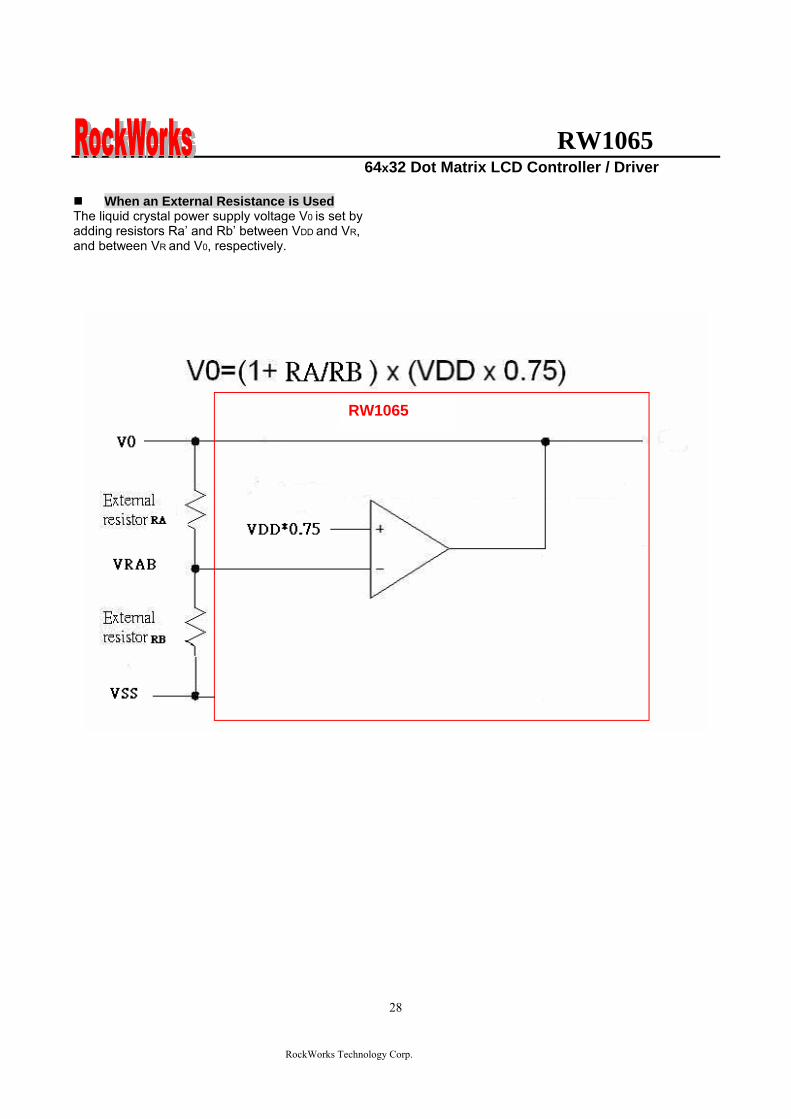
RW1065 64x32 Dot Matrix LCD Controller Driver
RockWorks Technology Corp
28
When an External Resistance is Used The liquid crystal power supply voltage V0 is set by adding resistors Rarsquo and Rbrsquo between VDD and VR and between VR and V0 respectively
RW1065
RW1065 64x32 Dot Matrix LCD Controller Driver
RockWorks Technology Corp
29
The set voltage circuits
Using the step-up voltage circuits equipped within the RW1065 chips it is possible to produce a 2X 3X 4X step-up voltage levels 2X step-up
To produce voltage level in the positive direction at the Vout terminal that is 2 times the voltage difference between VSS and VDD2 Please configure set voltage circuits like this Place a 1uF~22uF capacitor between CAP1N and CAP1P Place a 1uF~22uF capacitor between VSS and VOUT Short CAP2P CAP3P and VOUT Leave CAP2N open 3X step-up
To produce voltage level in the positive direction at the Vout terminal that is 3 times the voltage difference between VSS and VDD2 Please configure set voltage circuits like this Place a 1uF~22uF capacitor between CAP1N and CAP1P Place a 1uF~22uF capacitor between VSS and VOUT Place a 1uF~22uF capacitor and 100 ohms resistor between CAP2N and CAP2P Short CAP3P and Vout 4X step-up
To produce voltage level in the positive direction at the Vout terminal that is 4 times the voltage difference between VSS and VDD2 Please configure set voltage circuits like this Place a 1uF~22uF capacitor between CAP1N and CAP1P Place a 1uF~22uF capacitor between VSS and VOUT Place a 1uF~22uF capacitor and 100 ohms resistor between CAP2N and CAP2P Place a 1uF~22uF capacitor and 100 ohms resistor between CAP1N and CAP3P
RW1065 64x32 Dot Matrix LCD Controller Driver
RockWorks Technology Corp
30
ABSOLUTE MAXIMUM RATINGS Characteristics Symbol Value Unit
Power supply voltage VDD -03 to +70 V
LCD driver voltage Vout 0 to +17 V
Input voltage VIN -03 to VDD+03 V
Operating temperature TA -40 to +85
Storage temperature TSTO -55 to +125
DC CHARACTERISTICS
Rating Item Symbol Condition Min Typ Max Unit ApplicablePin
Operating Voltage VDD - 27 30 55 V VDD1
Step up output voltage Vout (Relative to VDD) 0 - 17 V Vout
Voltage follower circuit operating Voltage V0 (Relative to VDD) 0 - 15 V V0
V0 accuracy V0 - 0 - 15 V0
High-level Input Voltage Low-level Input Voltage
VIHC VILC - 07 VDD
Vss - VDD 09 V 2
High-level Output Voltage Low-level Output Voltage
VOHC VOLC
IOH = ndash05 mA IOL = 05 mA
08VDD Vss - VDD
02 VDD V 3
Input leakage current ILI VIN = VDD or VSS -1 - 2 uA 4
Output leakage current ILO - -1 1 uA 5
Liquid Crystal Driver ON Resistance RON
Ta= 25degC(Relative To VDD)
V0 =15 V - 16 20 KΩ SEGn COMn 6
Internal Oscillator fOSC 2286 254 2794 Oscillator
Frequency External Input RECOMMAND fCL
Ta = 25degC 132Duty 2286 254 2794
kHz CL
Internal Oscillator fOSC 45 5 55 Oscillator
Frequency External Input RECOMMAND fCL
Ta = 25degC 164Duty 45 5 55
kHz CL
bullDynamic Consumption Current During Display with the Internal Power Supply OFF Current consumed by total ICs when an external power supply is used
Unless otherwise specified Vss=0V VDD=30V
RW1065 64x32 Dot Matrix LCD Controller Driver
RockWorks Technology Corp
31
Display Pattern OFF
Ta = 25degC Vout=17V Rating Item Symbol Condition Min Typ Max Unit Notes
VDD=30 V V0-Vss=8V - 10 15 RW1065 IDD VDD=50 V V0-Vss=8V - 35 45
microA 7
Display Pattern Checker
Ta = 25degC Vout=17V Rating Item Symbol Condition Min Typ Max Unit Notes
VDD=30 V V0-Vss=8V - 15 20 RW1065 IDD VDD=50 V V0-Vss=8V - 40 50
microA 7
Display Pattern OFF
Ta = 25degC Vout=17V Rating Item Symbol Condition Min Typ Max Unit Notes
VDD=30 V V0-Vss=8V - 15 20 RW1065 IDD VDD=50 V V0-Vss=8V - 40 50
microA 7
Display pattern Checker
Ta = 25degC Vout=17V Rating Item Symbol Condition Min Typ Max Unit Notes
VDD=30 V V0-Vss=8V - 65 80 RW1065 IDD VDD=50 V V0-Vss=8V - 130 150
microA 7
bull Consumption Current at Time of Power Saver Mode VSS = 0 V VDD = 30 V plusmn 10
Rating Item Symbol Condition Min Typ Max Unit Notes
Sleep mode IDD - - 5 10 microA -
References for items market with 1 While a broad range of operating voltages is guaranteed performance cannot be guaranteed if there are sudden fluctuations to the
voltage while the MPU is being accessed 2 The RS D0 to D5 D6 D7 E RW CS1BP CS2P CLS CL FR MS and RST
― terminals
3 The D0 to D7 FR and CL terminals 4 The RS E RW CS1BP CS2P CLS MS and RST
― terminals
5 Applies when the D0 to D5 D6 D7 CL and FR terminals are in a high impedance state 6 These are the resistance values for when a 01 V voltage is applied between the output terminals SEGn or COMn and
the various power supply terminals (V1 V2 V3 and V4) These are specified for the operating voltage (3) range RON = 01 V ∆I (Where ∆I is the current that flows when 01 V is applied while the power supply is ON)
7 It indicates the current consumed on ICs alone when the internal oscillator circuit and display are turned on Does not include the current due to the LCD panel capacity and wiring capacity Applicable only when there is no access from the MPU
RW1065 64x32 Dot Matrix LCD Controller Driver
RockWorks Technology Corp
32
TIMING CHARACTERISTICS
68 Interface
(Ta=-40 to 85 degC) VDD=27 to 45V
Rating VDD=45 to 55V
Rating Item Signal Symbol ConditionMin Max Min Max
Units
Address hold time RS tAH6 0 mdash 0 mdash Address setup time RS tAW6
mdash 0 mdash 0 mdash
ns
System cycle time RS tCYC6 mdash 900 mdash 800 mdash ns Data setup time D0 to D7 tDS6 100 mdash 100 mdash Data hold time D0 to D7 tDH6
mdash 0 mdash 0 mdash
ns
Access time D0 to D7 tACC6 mdash 350 mdash 250
Output disable time D0 to D7 tOH6 CL = 100 pF
mdash 300 mdash 200 ns
Read tEWHR 360 mdash 300 mdash Enable H pulse time
WriteE
tEWHW mdash
360 mdash 300 mdash ns
Read tEWLR 450 mdash 400 mdash Enable L pulse time
WriteE
tEWLW mdash
450 mdash 400 mdash ns
1 All timing is specified using 20 and 80 of VDD as the reference 2 tEWLW and tEWLR are specified as the overlap between CS1BP being ldquoLrdquo (CS2P = ldquoHrdquo) and E
RW1065 64x32 Dot Matrix LCD Controller Driver
RockWorks Technology Corp
33
Reset Timing
Rating Item Signal Symbol Condition
Min Typ Max Units
Reset time mdash tR mdash mdash - 2 micros
Reset ldquoLrdquo pulse width RST tRW mdash 2 - mdash micros
1 When double chip was be used then the duty set command must be set between the tR
RW1065 64x32 Dot Matrix LCD Controller Driver
RockWorks Technology Corp
34
IO PAD CONFIGURATION
RW1065 64x32 Dot Matrix LCD Controller Driver
RockWorks Technology Corp
35
THE MPU INTERFACE (REFERENCE EXAMPLES) The RW1065 Series can be connected to 6800 Series MPUs The display area can be enlarged by using multiple RW1065 Series chips When this is done the chip select signal can be used to select the individual ICs to access
6800 Series MPUs
RW
106
5
RW1065 64x32 Dot Matrix LCD Controller Driver
RockWorks Technology Corp
36
When using external multi-level power supply for LCD driving (REFERENCE EXAMPLE)
Using a resistor divider can provide RW1065 external multi-level power supply for LCD driving
The circuit below shows a resistor divider network which can bias V0 V1 V2 V3 and V4 externally
RW1065 64x32 Dot Matrix LCD Controller Driver
RockWorks Technology Corp
37
bullWhen V0 V1 V2 V3 and V4 are biased by external power supply analog section of RW1065 should be turn off by software during LCD initialization The example in below shows the sequence to turn off analog section when external bias is used Begin of LCD initialization 1 Reset RW1065 2 SET EXT=1 (mode instruction)
RS RW DB7 DB6 DB5 DB4 DB3 DB2 DB1 DB00 0 0 0 0 0 1 1 0 1
3 SET Display Command (double command)
RS RW DB7 DB6 DB5 DB4 DB3 DB2 DB1 DB00 0 0 0 0 0 0 1 0 1 0 0 0 0 1 1 0 0 0 1
4 SET EXT=1 (mode instruction)
RS RW DB7 DB6 DB5 DB4 DB3 DB2 DB1 DB00 0 0 0 0 0 1 1 0 0
End of LCD initialization
bullBecause pins can not set LCD bias when external power supplies are used for LCD driving the bias can be set by an appropriate configuration for a resistor voltage divider networks The example is shown below
VSS
R
R
NR
R
R
RV1
RV2
RV3
RV4
V0
Bias Network Circuit Concept 15 Bias N=1 total = 5R 16 Bias N=2 total =6R 18 Bias N=4 total =8R 19 Bias N=5 total = 9R
RW1065 64x32 Dot Matrix LCD Controller Driver
RockWorks Technology Corp
38
Single chip solution for RW1065 application (REFERENCE EXAMPLE)
For a 64x32 application the duty cycle of LCD panel is 164 and the display duty of RW1065 should be set to 164 The display duty cycle can be selected by the DUTY bit in display command The diagram for 64x32 application is shown below
64 SEGx32COM LCD Panel
164 duty cycle
RW1065 DUTY=1
COM1~33
SEG1~65
RW1065 64x32 Dot Matrix LCD Controller Driver
RockWorks Technology Corp
39
Using an adjustable resistor on the main board to adjust the contrast of liquid crystal display (REFERENCE EXAMPLE)
The schematic shows an adjustable resistor on main board that can adjust voltage level of V0
RW1065 64x32 Dot Matrix LCD Controller Driver
RockWorks Technology Corp
40
Package information (Please pay close attention to the information in this section Do not hesitate to consult with our sale representative if you have any question or concern)
In order to make better bonding yield for RW1065 please follow the tips and recommendations in this section In this section few tips about COB footprint style PCB layout and wire bonding will be discussed
The drawing in below shows the PCB footprint style which we recommend for RW1065 Pads array in
curve shape is easier for Al wire bonding Besides that a real size COB footprint for RW1065 is also shown in below RW1065 COB footprint is also available in powerpcb or protel format for design reference purpose
The ratio is 11
RW1065 64x32 Dot Matrix LCD Controller Driver
RockWorks Technology Corp
41
During COB footprint design there have some tips about footprint that the PCB designer should know The angle between bonding wire and vertical line should less than 45 Otherwise the wire shorts would become very easy to happen at fours corners of the chip
The angle between bonding wire and vertical line could be reduced by expanding the distance between pads array and the chip In addition reducing length in horizon direction of pads array could minimize the angle between bonding wire and vertical line The picture in below will help to illustrate this concept From the experiences COB footprint style affects the bonding yield
Bad Wires are too close to each other
The angle between bonding wire and vertical line is greater than 45
The angle between bonding wire and vertical line is less than 45
Wires are not too close to each other
Reducing length in horizon direction of pads array could minimize the angle between bonding wire and vertical line
The angle between bonding wire and vertical line could be reduced by expanding the distance between pads array and the chip
RW1065 64x32 Dot Matrix LCD Controller Driver
RockWorks Technology Corp
42
If the gap between pads of COB footprint is filled with solder mask coating it is difficult to bond Al wire to
the pads The top solder masks layer that overlap COB footprint area should be removed
Please use 1 mils diameter Al wire for RW1065 wire bonding
1 2 3 4 5 6
A
B
C
D
654321
D
C
B
A
Title
Number RevisionSize
C
Date 29-Aug-2007 Sheet of File D公司資料99seMyDesignddb Drawn By
RW1065
COM131
COM142
COM153
COM164
COM175
COM186
COM197
COM208
COM219
COM2210
COM2311
COM2412
COM2513
COM2614
COM2715
COM2816
COM2917
COM3018
COM3119
SEG
6320
SEG
6221
SEG
6122
SEG
6023
SEG
5924
SEG
5825
SEG
5726
SEG
5627
SEG
5528
SEG
5429
SEG
5330
SEG
5231
SEG
5132
SEG
5033
SEG
4934
SEG
4835
SEG
4736
SEG
4637
SEG
4538
SEG
4439
SEG
4340
SEG
4241
SEG
4142
SEG
4043
SEG
3944
SEG
3845
SEG
3746
SEG
3647
SEG
3548
SEG
3449
SEG
3350
SEG
3251
SEG
3152
SEG
3053
SEG
2954
SEG
2855
SEG
2756
SEG
2657
SEG
2558
SEG
2459
SEG
2360
SEG
2261
SEG
2162
SEG
2063
SEG
1964
SEG
1865
SEG
1766
SEG
1667
SEG
1568
SEG
1469
SEG13 70SEG12 71SEG11 72SEG10 73SEG9 74SEG8 75SEG7 76SEG6 77SEG5 78SEG4 79SEG3 80SEG2 81SEG1 82SEG0 83ADCP 84CLL 85
VSS
86D
087
D1
88D
289
D3
90D
491
D5
92D
693
D7
94C
S1B
P95
CS2
P96
ERD
P97
AO
P(R
S)98
RW
RP
99V
DD
100
RST
P10
1C
LSP
102
FRR
103
MSP
104
BS1
P10
5B
S0P
106
SHLP
107
VD
D2
108
CA
P2N
109
CA
P2P
110
CA
P1P
111
CA
P1N
112
CA
P3P
113
VO
UT
114
V0
115
VR
AB
116
V3
117
V2
118
V4
119
V1
120
CO
M0
121
CO
M1
122
CO
M2
123
CO
M3
124
CO
M4
125
CO
M5
126
CO
M6
127
CO
M7
128
CO
M8
129
CO
M9
130
CO
M10
131
CO
M11
132
CO
M12
133
4897x1902 um
IC1
RW1065
C9CAPR4
100R0603
R30R0603
C8
CAP
C7
CAP
R2
100R0603
R1
0R0603C6 22uf
R50R
R6300R
R7RES1
R8NC R9
100R0603
VDD
R10
NC
R11
100R0603
R12
100R0603
R13
NC
R14
100R0603
R15
NC
VDD
D0
D1
D2
D3
D4
D5
D6
D7
DB[07]
VDDC5
01uf0603
VD
D
CS2
P
123456789
1011121314151617181920
J1
CON20
C1201uf0603
R3951K0603
VDD
CAP Value1UF~22UF
2XPut C6C8 Short R1R3Open R2R4C7C93XPut C6C8C9 R4Short R1Open R2R3C74XOpen R1R3
BS0 BS1 Bias0 0
0 1
1 0
11
15 bias
16 bias
18 bias
19 bias
ADC=0 SEG0lt~column address 00Hnormal(default) ADC=1 SEG0lt~column address 3FHinverted
SHL=0 Normal COM0~gtCOM63(default)SHL=1 Reverse direction COM63~gtCOM0
R16100R0603
LCD PANEL 64X32RockWorks
RW1065 64X32
COM0-31 SEG0-63SHL=0 ADC=0
SHL=1COM31-0
ADC=1SEG63-0
if use single chip for 32 command displaythe display command must select 164 dutyDisplay panel must select 164 duty type
VO
UT
C3P
C1N
C1P
C2P
C2N
VDD2
ADC
SHL
BS0
BS1
CLLADC
V1
V2
V3
V4
VR
AB
V0
VO
UT
C3P
C1N
C1P
C2P
C2N
VD
D2
SHL
BS0
BS1
FRR
RST
P
RW
RS
E CS1
B
CS1
V0RSRWED0D1D2D3D4D5D6D7
RSTPAK
C4
22uf
RBRES1
RA1RES1
C2
22uf
C1
22uf
C3
22uf
C0
22uf
R20
100k0603
R21
100k0603
R17
200K0603
V1
V2
V3
V4 VRAB
V0
V0
OPTION
B
R18
300R0603
RA2RES1
VADJ
R19100R
R23 RES1R22 0R
R24
RES1
R25
0R
VDD
CS1BP
CS2P
CS1
CS1
R26
22R0603
R27
22R0603
C1047uf
C11
01uf
VSS_INVDD_IN
D1DIODE
FGND
鐵框地
VSS
VDD
R28 10RR29 10RR30 10RR31 10RR32 10RR33 10RR34 10RR35 10RR36 10RR37 10RR38 10R
VADJ
1 2 3 4 5 6
A
B
C
D
654321
D
C
B
A
Title
Number RevisionSize
C
Date 29-Aug-2007 Sheet of File D公司資料99seMyDesignddb Drawn By
RW1065
COM131
COM142
COM153
COM164
COM175
COM186
COM197
COM208
COM219
COM2210
COM2311
COM2412
COM2513
COM2614
COM2715
COM2816
COM2917
COM3018
COM3119
SEG
6320
SEG
6221
SEG
6122
SEG
6023
SEG
5924
SEG
5825
SEG
5726
SEG
5627
SEG
5528
SEG
5429
SEG
5330
SEG
5231
SEG
5132
SEG
5033
SEG
4934
SEG
4835
SEG
4736
SEG
4637
SEG
4538
SEG
4439
SEG
4340
SEG
4241
SEG
4142
SEG
4043
SEG
3944
SEG
3845
SEG
3746
SEG
3647
SEG
3548
SEG
3449
SEG
3350
SEG
3251
SEG
3152
SEG
3053
SEG
2954
SEG
2855
SEG
2756
SEG
2657
SEG
2558
SEG
2459
SEG
2360
SEG
2261
SEG
2162
SEG
2063
SEG
1964
SEG
1865
SEG
1766
SEG
1667
SEG
1568
SEG
1469
SEG13 70SEG12 71SEG11 72SEG10 73SEG9 74SEG8 75SEG7 76SEG6 77SEG5 78SEG4 79SEG3 80SEG2 81SEG1 82SEG0 83ADCP 84CLL 85
VSS
86D
087
D1
88D
289
D3
90D
491
D5
92D
693
D7
94C
S1B
P95
CS2
P96
ERD
P97
AO
P(R
S)98
RW
RP
99V
DD
100
RST
P10
1C
LSP
102
FRR
103
MSP
104
BS1
P10
5B
S0P
106
SHLP
107
VD
D2
108
CA
P2N
109
CA
P2P
110
CA
P1P
111
CA
P1N
112
CA
P3P
113
VO
UT
114
V0
115
VR
AB
116
V3
117
V2
118
V4
119
V1
120
CO
M0
121
CO
M1
122
CO
M2
123
CO
M3
124
CO
M4
125
CO
M5
126
CO
M6
127
CO
M7
128
CO
M8
129
CO
M9
130
CO
M10
131
CO
M11
132
CO
M12
133
4897x1902 um
IC1
RW1065 Master
RW1065
COM131
COM142
COM153
COM164
COM175
COM186
COM197
COM208
COM219
COM2210
COM2311
COM2412
COM2513
COM2614
COM2715
COM2816
COM2917
COM3018
COM3119
SEG
6320
SEG
6221
SEG
6122
SEG
6023
SEG
5924
SEG
5825
SEG
5726
SEG
5627
SEG
5528
SEG
5429
SEG
5330
SEG
5231
SEG
5132
SEG
5033
SEG
4934
SEG
4835
SEG
4736
SEG
4637
SEG
4538
SEG
4439
SEG
4340
SEG
4241
SEG
4142
SEG
4043
SEG
3944
SEG
3845
SEG
3746
SEG
3647
SEG
3548
SEG
3449
SEG
3350
SEG
3251
SEG
3152
SEG
3053
SEG
2954
SEG
2855
SEG
2756
SEG
2657
SEG
2558
SEG
2459
SEG
2360
SEG
2261
SEG
2162
SEG
2063
SEG
1964
SEG
1865
SEG
1766
SEG
1667
SEG
1568
SEG
1469
SEG13 70SEG12 71SEG11 72SEG10 73SEG9 74SEG8 75SEG7 76SEG6 77SEG5 78SEG4 79SEG3 80SEG2 81SEG1 82SEG0 83ADCP 84CLL 85
VSS
86D
087
D1
88D
289
D3
90D
491
D5
92D
693
D7
94C
S1B
P95
CS2
P96
ERD
P97
AO
P(R
S)98
RW
RP
99V
DD
100
RST
P10
1C
LSP
102
FRR
103
MSP
104
BS1
P10
5B
S0P
106
SHLP
107
VD
D2
108
CA
P2N
109
CA
P2P
110
CA
P1P
111
CA
P1N
112
CA
P3P
113
VO
UT
114
V0
115
VR
AB
116
V3
117
V2
118
V4
119
V1
120
CO
M0
121
CO
M1
122
CO
M2
123
CO
M3
124
CO
M4
125
CO
M5
126
CO
M6
127
CO
M7
128
CO
M8
129
CO
M9
130
CO
M10
131
CO
M11
132
CO
M12
133
4897x1902 um
IC2
RW1065 Slave
C4
22uf
RBRES1
RA1RES1
C2
22uf
C1
22uf
C3
22uf
C0
22ufC9CAPR4
100R0603
R30R0603
C8
CAP
C7
CAP
R2
100R0603
R1
0R0603C6 22uf
R50R0603
R6300R0603
R7RES1
R8NC R9
100R0603
VDD
R10
NC
R11
100R0603
R12
NC
R13
100R0603
R14
100R0603
R15
NC
R16
100R0603
R17
NC
VDD
D0
D1
D2
D3
D4
D5
D6
D7
D0
D1
D2
D3
D4
D5
D6
D7
DB[07] DB[07]
VDDC10
01uf0603
VD
D
IC1_
CS2
P
VDD
IC2_
CS2
P
VD
D
C11
01uf0603
VSS
VSS
LCD PANEL 128X64
Master COM0-31 Slave COM32-63
Master SEG0-63 Slave SEG64-127
123456789
1011121314151617181920
J1
CON20
Master Slave
CAP Value1UF~22UF
2XPut C6C8 Short R1R3Open R2R4C7C93XPut C6C8C9 R4Short R1Open R2R3C74XOpen R1R3
RockWorksRW1065 128x64
BS0 BS1 Bias0 0
0 1
1 0
11
15 bias
16 bias
18 bias
19 bias
ADC=0 SEG0lt~column address 00Hnormal(default) ADC=1 SEG0lt~column address 3FHinverted
SHL=0 Normal COM0~gtCOM63(default)SHL=1 Reverse direction COM63~gtCOM0Both Master and Slave should set identical SHL value
SHL=0 SHL=0
ADC=0 ADC=0
Slave COM31-0
Slave SEG127-64
SHL=1
ADC=1
SHL=1Master COM63-32
ADC=1Master SEG63-0
R18100R0603
R22
100k0603
R23
100k0603
C501uF0603
R4551K0603
VDD
R19
200K0603
ADC1
ADC2
SHL
BS0
BS1
VDD2
V1
V2
V3
V4 VRAB
V0
V0V
OU
T
C3P
C1N
C1P
C2P
C2N
V1
V2
V3
V4
VR
AB
V0
VO
UT
C3P
C1N
C1P
C2P
C2N
VD
D2
SHL
BS0
BS1
FRR
RST
P
RW
RS
E IC1_
CS1
BP
V1
V2
V3
V4
VR
AB
V0
VO
UT
VD
D2
SHL
BS0
BS1
FRR
RST
P
RW
RS
E IC2_
CS1
BP
CLLADC1
CLLADC2
RSTP
CS1CS2
V0RSRWED0D1D2D3D4D5D6D7
AK
OPTION
R20
300R0603
RA2RES1
VADJ
R21
100R
B
R25 RESR24 0R
R26 RES R27 0RVDD
IC1_CS1BP
IC1_CS2P
CS1
CS1
R28 0R R29 RES
R30 RES R31 0R
IC2_CS1BP
IC2_CS2P
CS2
CS2
R32
22R0603
R33
22R0603
C1001uf
C11
47uf
D1DIODE
FGND
鐵框地
VSS
VDD
R34 10RR35 10RR36 10RR37 10RR38 10RR39 10RR40 10RR41 10RR42 10RR43 10RR44 10R
VSS_INVDD_IN
VADJ
VDD
1 2 3 4 5 6 7 8
A
B
C
D
87654321
D
C
B
A
Title
Number RevisionSize
D
Date 29-Aug-2007 Sheet of File D公司資料 99seMyDesignddb Drawn By
C422uf
RBRES1
RA1RES1
C3
22uf
C2
22uf
C1
22uf
C0
22ufC9CAPR4
100R0603
R30R0603
C8
CAP
C7
CAP
R2
100R0603
R1
0R0603C6 22uf
R220R0603
R23300R0603
R24RES1
R39
NCR40
100 ohm0603
VDD
R41
NC
R42
100 ohm0603
R43
NC
R44
100 ohm0603
R45
NC
R46
100 ohm0603
R47
100 ohm0603
R48
NC
R49
100 ohm0603
R50
NC
VDDCAP Value1UF~22UF
2XPut C6C8 Short R1R3Open R2R4C7C93XPut C6C8C9 R4Short R1Open R2R3C74XOpen R1R3
BS0 BS1 Bias0 0
0 1
1 0
11
15 bias
16 bias
18 bias
19 bias
ADC=0 SEG0lt~column address 00Hnormal(default)
ADC=1 SEG0lt~column address 3FHinverted
SHL=0 Normal COM0~gtCOM63(default)SHL=1 Reverse direction COM63~gtCOM0Both Master and Slave should set identical SHL value
R7
100k0603
R8
100k0603
V1
V2
V3
V4
V0
VRAB
V0
R5
200K
VDD2
VO
UT
C3P
C1N
C1P
C2P
C2N
ADC1
ADC2
ADC3
SHL
BS0
BS1
CS1CS2CS3
V0RSRWED0D1D2D3D4D5D6D7
RSTP
R3851K0603
C5
01uF
VDD
OPTION
R6
300R0603R9100R
RA2RES1
VADJ
RW1065
COM131
COM142
COM153
COM164
COM175
COM186
COM197
COM208
COM219
COM2210
COM2311
COM2412
COM2513
COM2614
COM2715
COM2816
COM2917
COM3018
COM3119
SEG
6320
SEG
6221
SEG
6122
SEG
6023
SEG
5924
SEG
5825
SEG
5726
SEG
5627
SEG
5528
SEG
5429
SEG
5330
SEG
5231
SEG
5132
SEG
5033
SEG
4934
SEG
4835
SEG
4736
SEG
4637
SEG
4538
SEG
4439
SEG
4340
SEG
4241
SEG
4142
SEG
4043
SEG
3944
SEG
3845
SEG
3746
SEG
3647
SEG
3548
SEG
3449
SEG
3350
SEG
3251
SEG
3152
SEG
3053
SEG
2954
SEG
2855
SEG
2756
SEG
2657
SEG
2558
SEG
2459
SEG
2360
SEG
2261
SEG
2162
SEG
2063
SEG
1964
SEG
1865
SEG
1766
SEG
1667
SEG
1568
SEG
1469
SEG13 70SEG12 71SEG11 72SEG10 73SEG9 74SEG8 75SEG7 76SEG6 77SEG5 78SEG4 79SEG3 80SEG2 81SEG1 82SEG0 83ADCP 84CLL 85
VSS
86D
087
D1
88D
289
D3
90D
491
D5
92D
693
D7
94C
S1B
P95
CS2
P96
ERD
P97
AO
P(R
S)98
RW
RP
99V
DD
100
RST
P10
1C
LSP
102
FRR
103
MSP
104
BS1
P10
5B
S0P
106
SHLP
107
VD
D2
108
CA
P2N
109
CA
P2P
110
CA
P1P
111
CA
P1N
112
CA
P3P
113
VO
UT
114
V0
115
VR
AB
116
V3
117
V2
118
V4
119
V1
120
CO
M0
121
CO
M1
122
CO
M2
123
CO
M3
124
CO
M4
125
CO
M5
126
CO
M6
127
CO
M7
128
CO
M8
129
CO
M9
130
CO
M10
131
CO
M11
132
CO
M12
133
4897x1902 um
IC1
RW1065 Master
RW1065
COM131
COM142
COM153
COM164
COM175
COM186
COM197
COM208
COM219
COM2210
COM2311
COM2412
COM2513
COM2614
COM2715
COM2816
COM2917
COM3018
COM3119
SEG
6320
SEG
6221
SEG
6122
SEG
6023
SEG
5924
SEG
5825
SEG
5726
SEG
5627
SEG
5528
SEG
5429
SEG
5330
SEG
5231
SEG
5132
SEG
5033
SEG
4934
SEG
4835
SEG
4736
SEG
4637
SEG
4538
SEG
4439
SEG
4340
SEG
4241
SEG
4142
SEG
4043
SEG
3944
SEG
3845
SEG
3746
SEG
3647
SEG
3548
SEG
3449
SEG
3350
SEG
3251
SEG
3152
SEG
3053
SEG
2954
SEG
2855
SEG
2756
SEG
2657
SEG
2558
SEG
2459
SEG
2360
SEG
2261
SEG
2162
SEG
2063
SEG
1964
SEG
1865
SEG
1766
SEG
1667
SEG
1568
SEG
1469
SEG13 70SEG12 71SEG11 72SEG10 73SEG9 74SEG8 75SEG7 76SEG6 77SEG5 78SEG4 79SEG3 80SEG2 81SEG1 82SEG0 83ADCP 84CLL 85
VSS
86D
087
D1
88D
289
D3
90D
491
D5
92D
693
D7
94C
S1B
P95
CS2
P96
ERD
P97
AO
P(R
S)98
RW
RP
99V
DD
100
RST
P10
1C
LSP
102
FRR
103
MSP
104
BS1
P10
5B
S0P
106
SHLP
107
VD
D2
108
CA
P2N
109
CA
P2P
110
CA
P1P
111
CA
P1N
112
CA
P3P
113
VO
UT
114
V0
115
VR
AB
116
V3
117
V2
118
V4
119
V1
120
CO
M0
121
CO
M1
122
CO
M2
123
CO
M3
124
CO
M4
125
CO
M5
126
CO
M6
127
CO
M7
128
CO
M8
129
CO
M9
130
CO
M10
131
CO
M11
132
CO
M12
133
4897x1902 um
IC2
RW1065 Slave
D0
D1
D2
D3
D4
D5
D6
D7
D0
D1
D2
D3
D4
D5
D6
D7
DB[07] DB[07]
VDDC8
01uf0603
VD
D
VDD
VD
D
C9
01uf0603
VSS
VSS
LCD PANEL 192X64
Master COM0-31 Slave COM32-63
Master SEG0-63 Slave SEG64-127
Master Slave
RockWorksRW1065 192x64
RW1065
COM131
COM142
COM153
COM164
COM175
COM186
COM197
COM208
COM219
COM2210
COM2311
COM2412
COM2513
COM2614
COM2715
COM2816
COM2917
COM3018
COM3119
SEG
6320
SEG
6221
SEG
6122
SEG
6023
SEG
5924
SEG
5825
SEG
5726
SEG
5627
SEG
5528
SEG
5429
SEG
5330
SEG
5231
SEG
5132
SEG
5033
SEG
4934
SEG
4835
SEG
4736
SEG
4637
SEG
4538
SEG
4439
SEG
4340
SEG
4241
SEG
4142
SEG
4043
SEG
3944
SEG
3845
SEG
3746
SEG
3647
SEG
3548
SEG
3449
SEG
3350
SEG
3251
SEG
3152
SEG
3053
SEG
2954
SEG
2855
SEG
2756
SEG
2657
SEG
2558
SEG
2459
SEG
2360
SEG
2261
SEG
2162
SEG
2063
SEG
1964
SEG
1865
SEG
1766
SEG
1667
SEG
1568
SEG
1469
SEG13 70SEG12 71SEG11 72SEG10 73SEG9 74SEG8 75SEG7 76SEG6 77SEG5 78SEG4 79SEG3 80SEG2 81SEG1 82SEG0 83ADCP 84CLL 85
VSS
86D
087
D1
88D
289
D3
90D
491
D5
92D
693
D7
94C
S1B
P95
CS2
P96
ERD
P97
AO
P(R
S)98
RW
RP
99V
DD
100
RST
P10
1C
LSP
102
FRR
103
MSP
104
BS1
P10
5B
S0P
106
SHLP
107
VD
D2
108
CA
P2N
109
CA
P2P
110
CA
P1P
111
CA
P1N
112
CA
P3P
113
VO
UT
114
V0
115
VR
AB
116
V3
117
V2
118
V4
119
V1
120
CO
M0
121
CO
M1
122
CO
M2
123
CO
M3
124
CO
M4
125
CO
M5
126
CO
M6
127
CO
M7
128
CO
M8
129
CO
M9
130
CO
M10
131
CO
M11
132
CO
M12
133
4897x1902 um
IC3
RW1065 Slave
D0
D1
D2
D3
D4
D5
D6
D7
DB[07]
VSS
VSS
VDD
VD
D
C10
01uf0603
Slave SEG128-192
Slave
SHL=0 SHL=0
Master COM63-32SHL=1 SHL=1
Slave COM31-0ADC=0 ADC=0 ADC=0
ADC=1 ADC=1 ADC=1Master SEG63-0 Slave SEG127-64 Slave SEG192-128
R50100R0603
V1
V2
V3
V4
VR
AB
V0
VO
UT
C3P
C1N
C1P
C2P
C2N
VD
D2
SHL
BS0
BS1
FRR
RST
P
RW
RS
E V1
V2
V3
V4
VR
AB
V0
VO
UT
VD
D2
SHL
BS0
BS1
FRR
RST
P
RW
RS
E V1
V2
V3
V4
VR
AB
V0
VO
UT
VD
D2
SHL
BS0
BS1
FRR
RST
P
RW
RS
E
CLL CLL CLLADC1 ADC2 ADC3
R25 10RR26 10RR27 10RR28 10RR29 10RR30 10RR31 10RR32 10RR33 10RR34 10RR35 10R
R36
22R0603
D1DIODE
R3722R0603
C647uf
C701uf
VSS_INVDD_IN
VSS
VDD
VADJ
123456789
101112131415161718192021222324
J1
CON24
AK
FGND
鐵框地
IC1_
CS1
BP
IC1_
CS2
P
IC2_
CS2
PIC
2_C
S1B
P
IC3_
CS1
BP
IC3_
CS2
B
R10 0R R11 RES
R12 RES R13 0RVDD
IC1_CS2B
IC1_CS1BPCS1
CS1
R14 0R R15 RES
R16 RES R17 0RVDDIC2_CS2B
IC2_CS1BPCS2
CS2
R18 0R R19 RES
R20 RES R21 0RVDDIC3_CS2B
IC3_CS1BPCS3
CS3
B
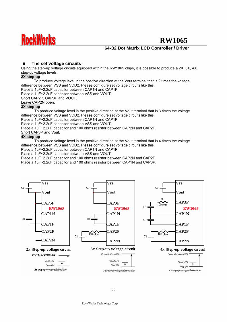
RW1065 64x32 Dot Matrix LCD Controller Driver
RockWorks Technology Corp
30
ABSOLUTE MAXIMUM RATINGS Characteristics Symbol Value Unit
Power supply voltage VDD -03 to +70 V
LCD driver voltage Vout 0 to +17 V
Input voltage VIN -03 to VDD+03 V
Operating temperature TA -40 to +85
Storage temperature TSTO -55 to +125
DC CHARACTERISTICS
Rating Item Symbol Condition Min Typ Max Unit ApplicablePin
Operating Voltage VDD - 27 30 55 V VDD1
Step up output voltage Vout (Relative to VDD) 0 - 17 V Vout
Voltage follower circuit operating Voltage V0 (Relative to VDD) 0 - 15 V V0
V0 accuracy V0 - 0 - 15 V0
High-level Input Voltage Low-level Input Voltage
VIHC VILC - 07 VDD
Vss - VDD 09 V 2
High-level Output Voltage Low-level Output Voltage
VOHC VOLC
IOH = ndash05 mA IOL = 05 mA
08VDD Vss - VDD
02 VDD V 3
Input leakage current ILI VIN = VDD or VSS -1 - 2 uA 4
Output leakage current ILO - -1 1 uA 5
Liquid Crystal Driver ON Resistance RON
Ta= 25degC(Relative To VDD)
V0 =15 V - 16 20 KΩ SEGn COMn 6
Internal Oscillator fOSC 2286 254 2794 Oscillator
Frequency External Input RECOMMAND fCL
Ta = 25degC 132Duty 2286 254 2794
kHz CL
Internal Oscillator fOSC 45 5 55 Oscillator
Frequency External Input RECOMMAND fCL
Ta = 25degC 164Duty 45 5 55
kHz CL
bullDynamic Consumption Current During Display with the Internal Power Supply OFF Current consumed by total ICs when an external power supply is used
Unless otherwise specified Vss=0V VDD=30V
RW1065 64x32 Dot Matrix LCD Controller Driver
RockWorks Technology Corp
31
Display Pattern OFF
Ta = 25degC Vout=17V Rating Item Symbol Condition Min Typ Max Unit Notes
VDD=30 V V0-Vss=8V - 10 15 RW1065 IDD VDD=50 V V0-Vss=8V - 35 45
microA 7
Display Pattern Checker
Ta = 25degC Vout=17V Rating Item Symbol Condition Min Typ Max Unit Notes
VDD=30 V V0-Vss=8V - 15 20 RW1065 IDD VDD=50 V V0-Vss=8V - 40 50
microA 7
Display Pattern OFF
Ta = 25degC Vout=17V Rating Item Symbol Condition Min Typ Max Unit Notes
VDD=30 V V0-Vss=8V - 15 20 RW1065 IDD VDD=50 V V0-Vss=8V - 40 50
microA 7
Display pattern Checker
Ta = 25degC Vout=17V Rating Item Symbol Condition Min Typ Max Unit Notes
VDD=30 V V0-Vss=8V - 65 80 RW1065 IDD VDD=50 V V0-Vss=8V - 130 150
microA 7
bull Consumption Current at Time of Power Saver Mode VSS = 0 V VDD = 30 V plusmn 10
Rating Item Symbol Condition Min Typ Max Unit Notes
Sleep mode IDD - - 5 10 microA -
References for items market with 1 While a broad range of operating voltages is guaranteed performance cannot be guaranteed if there are sudden fluctuations to the
voltage while the MPU is being accessed 2 The RS D0 to D5 D6 D7 E RW CS1BP CS2P CLS CL FR MS and RST
― terminals
3 The D0 to D7 FR and CL terminals 4 The RS E RW CS1BP CS2P CLS MS and RST
― terminals
5 Applies when the D0 to D5 D6 D7 CL and FR terminals are in a high impedance state 6 These are the resistance values for when a 01 V voltage is applied between the output terminals SEGn or COMn and
the various power supply terminals (V1 V2 V3 and V4) These are specified for the operating voltage (3) range RON = 01 V ∆I (Where ∆I is the current that flows when 01 V is applied while the power supply is ON)
7 It indicates the current consumed on ICs alone when the internal oscillator circuit and display are turned on Does not include the current due to the LCD panel capacity and wiring capacity Applicable only when there is no access from the MPU
RW1065 64x32 Dot Matrix LCD Controller Driver
RockWorks Technology Corp
32
TIMING CHARACTERISTICS
68 Interface
(Ta=-40 to 85 degC) VDD=27 to 45V
Rating VDD=45 to 55V
Rating Item Signal Symbol ConditionMin Max Min Max
Units
Address hold time RS tAH6 0 mdash 0 mdash Address setup time RS tAW6
mdash 0 mdash 0 mdash
ns
System cycle time RS tCYC6 mdash 900 mdash 800 mdash ns Data setup time D0 to D7 tDS6 100 mdash 100 mdash Data hold time D0 to D7 tDH6
mdash 0 mdash 0 mdash
ns
Access time D0 to D7 tACC6 mdash 350 mdash 250
Output disable time D0 to D7 tOH6 CL = 100 pF
mdash 300 mdash 200 ns
Read tEWHR 360 mdash 300 mdash Enable H pulse time
WriteE
tEWHW mdash
360 mdash 300 mdash ns
Read tEWLR 450 mdash 400 mdash Enable L pulse time
WriteE
tEWLW mdash
450 mdash 400 mdash ns
1 All timing is specified using 20 and 80 of VDD as the reference 2 tEWLW and tEWLR are specified as the overlap between CS1BP being ldquoLrdquo (CS2P = ldquoHrdquo) and E
RW1065 64x32 Dot Matrix LCD Controller Driver
RockWorks Technology Corp
33
Reset Timing
Rating Item Signal Symbol Condition
Min Typ Max Units
Reset time mdash tR mdash mdash - 2 micros
Reset ldquoLrdquo pulse width RST tRW mdash 2 - mdash micros
1 When double chip was be used then the duty set command must be set between the tR
RW1065 64x32 Dot Matrix LCD Controller Driver
RockWorks Technology Corp
34
IO PAD CONFIGURATION
RW1065 64x32 Dot Matrix LCD Controller Driver
RockWorks Technology Corp
35
THE MPU INTERFACE (REFERENCE EXAMPLES) The RW1065 Series can be connected to 6800 Series MPUs The display area can be enlarged by using multiple RW1065 Series chips When this is done the chip select signal can be used to select the individual ICs to access
6800 Series MPUs
RW
106
5
RW1065 64x32 Dot Matrix LCD Controller Driver
RockWorks Technology Corp
36
When using external multi-level power supply for LCD driving (REFERENCE EXAMPLE)
Using a resistor divider can provide RW1065 external multi-level power supply for LCD driving
The circuit below shows a resistor divider network which can bias V0 V1 V2 V3 and V4 externally
RW1065 64x32 Dot Matrix LCD Controller Driver
RockWorks Technology Corp
37
bullWhen V0 V1 V2 V3 and V4 are biased by external power supply analog section of RW1065 should be turn off by software during LCD initialization The example in below shows the sequence to turn off analog section when external bias is used Begin of LCD initialization 1 Reset RW1065 2 SET EXT=1 (mode instruction)
RS RW DB7 DB6 DB5 DB4 DB3 DB2 DB1 DB00 0 0 0 0 0 1 1 0 1
3 SET Display Command (double command)
RS RW DB7 DB6 DB5 DB4 DB3 DB2 DB1 DB00 0 0 0 0 0 0 1 0 1 0 0 0 0 1 1 0 0 0 1
4 SET EXT=1 (mode instruction)
RS RW DB7 DB6 DB5 DB4 DB3 DB2 DB1 DB00 0 0 0 0 0 1 1 0 0
End of LCD initialization
bullBecause pins can not set LCD bias when external power supplies are used for LCD driving the bias can be set by an appropriate configuration for a resistor voltage divider networks The example is shown below
VSS
R
R
NR
R
R
RV1
RV2
RV3
RV4
V0
Bias Network Circuit Concept 15 Bias N=1 total = 5R 16 Bias N=2 total =6R 18 Bias N=4 total =8R 19 Bias N=5 total = 9R
RW1065 64x32 Dot Matrix LCD Controller Driver
RockWorks Technology Corp
38
Single chip solution for RW1065 application (REFERENCE EXAMPLE)
For a 64x32 application the duty cycle of LCD panel is 164 and the display duty of RW1065 should be set to 164 The display duty cycle can be selected by the DUTY bit in display command The diagram for 64x32 application is shown below
64 SEGx32COM LCD Panel
164 duty cycle
RW1065 DUTY=1
COM1~33
SEG1~65
RW1065 64x32 Dot Matrix LCD Controller Driver
RockWorks Technology Corp
39
Using an adjustable resistor on the main board to adjust the contrast of liquid crystal display (REFERENCE EXAMPLE)
The schematic shows an adjustable resistor on main board that can adjust voltage level of V0
RW1065 64x32 Dot Matrix LCD Controller Driver
RockWorks Technology Corp
40
Package information (Please pay close attention to the information in this section Do not hesitate to consult with our sale representative if you have any question or concern)
In order to make better bonding yield for RW1065 please follow the tips and recommendations in this section In this section few tips about COB footprint style PCB layout and wire bonding will be discussed
The drawing in below shows the PCB footprint style which we recommend for RW1065 Pads array in
curve shape is easier for Al wire bonding Besides that a real size COB footprint for RW1065 is also shown in below RW1065 COB footprint is also available in powerpcb or protel format for design reference purpose
The ratio is 11
RW1065 64x32 Dot Matrix LCD Controller Driver
RockWorks Technology Corp
41
During COB footprint design there have some tips about footprint that the PCB designer should know The angle between bonding wire and vertical line should less than 45 Otherwise the wire shorts would become very easy to happen at fours corners of the chip
The angle between bonding wire and vertical line could be reduced by expanding the distance between pads array and the chip In addition reducing length in horizon direction of pads array could minimize the angle between bonding wire and vertical line The picture in below will help to illustrate this concept From the experiences COB footprint style affects the bonding yield
Bad Wires are too close to each other
The angle between bonding wire and vertical line is greater than 45
The angle between bonding wire and vertical line is less than 45
Wires are not too close to each other
Reducing length in horizon direction of pads array could minimize the angle between bonding wire and vertical line
The angle between bonding wire and vertical line could be reduced by expanding the distance between pads array and the chip
RW1065 64x32 Dot Matrix LCD Controller Driver
RockWorks Technology Corp
42
If the gap between pads of COB footprint is filled with solder mask coating it is difficult to bond Al wire to
the pads The top solder masks layer that overlap COB footprint area should be removed
Please use 1 mils diameter Al wire for RW1065 wire bonding
1 2 3 4 5 6
A
B
C
D
654321
D
C
B
A
Title
Number RevisionSize
C
Date 29-Aug-2007 Sheet of File D公司資料99seMyDesignddb Drawn By
RW1065
COM131
COM142
COM153
COM164
COM175
COM186
COM197
COM208
COM219
COM2210
COM2311
COM2412
COM2513
COM2614
COM2715
COM2816
COM2917
COM3018
COM3119
SEG
6320
SEG
6221
SEG
6122
SEG
6023
SEG
5924
SEG
5825
SEG
5726
SEG
5627
SEG
5528
SEG
5429
SEG
5330
SEG
5231
SEG
5132
SEG
5033
SEG
4934
SEG
4835
SEG
4736
SEG
4637
SEG
4538
SEG
4439
SEG
4340
SEG
4241
SEG
4142
SEG
4043
SEG
3944
SEG
3845
SEG
3746
SEG
3647
SEG
3548
SEG
3449
SEG
3350
SEG
3251
SEG
3152
SEG
3053
SEG
2954
SEG
2855
SEG
2756
SEG
2657
SEG
2558
SEG
2459
SEG
2360
SEG
2261
SEG
2162
SEG
2063
SEG
1964
SEG
1865
SEG
1766
SEG
1667
SEG
1568
SEG
1469
SEG13 70SEG12 71SEG11 72SEG10 73SEG9 74SEG8 75SEG7 76SEG6 77SEG5 78SEG4 79SEG3 80SEG2 81SEG1 82SEG0 83ADCP 84CLL 85
VSS
86D
087
D1
88D
289
D3
90D
491
D5
92D
693
D7
94C
S1B
P95
CS2
P96
ERD
P97
AO
P(R
S)98
RW
RP
99V
DD
100
RST
P10
1C
LSP
102
FRR
103
MSP
104
BS1
P10
5B
S0P
106
SHLP
107
VD
D2
108
CA
P2N
109
CA
P2P
110
CA
P1P
111
CA
P1N
112
CA
P3P
113
VO
UT
114
V0
115
VR
AB
116
V3
117
V2
118
V4
119
V1
120
CO
M0
121
CO
M1
122
CO
M2
123
CO
M3
124
CO
M4
125
CO
M5
126
CO
M6
127
CO
M7
128
CO
M8
129
CO
M9
130
CO
M10
131
CO
M11
132
CO
M12
133
4897x1902 um
IC1
RW1065
C9CAPR4
100R0603
R30R0603
C8
CAP
C7
CAP
R2
100R0603
R1
0R0603C6 22uf
R50R
R6300R
R7RES1
R8NC R9
100R0603
VDD
R10
NC
R11
100R0603
R12
100R0603
R13
NC
R14
100R0603
R15
NC
VDD
D0
D1
D2
D3
D4
D5
D6
D7
DB[07]
VDDC5
01uf0603
VD
D
CS2
P
123456789
1011121314151617181920
J1
CON20
C1201uf0603
R3951K0603
VDD
CAP Value1UF~22UF
2XPut C6C8 Short R1R3Open R2R4C7C93XPut C6C8C9 R4Short R1Open R2R3C74XOpen R1R3
BS0 BS1 Bias0 0
0 1
1 0
11
15 bias
16 bias
18 bias
19 bias
ADC=0 SEG0lt~column address 00Hnormal(default) ADC=1 SEG0lt~column address 3FHinverted
SHL=0 Normal COM0~gtCOM63(default)SHL=1 Reverse direction COM63~gtCOM0
R16100R0603
LCD PANEL 64X32RockWorks
RW1065 64X32
COM0-31 SEG0-63SHL=0 ADC=0
SHL=1COM31-0
ADC=1SEG63-0
if use single chip for 32 command displaythe display command must select 164 dutyDisplay panel must select 164 duty type
VO
UT
C3P
C1N
C1P
C2P
C2N
VDD2
ADC
SHL
BS0
BS1
CLLADC
V1
V2
V3
V4
VR
AB
V0
VO
UT
C3P
C1N
C1P
C2P
C2N
VD
D2
SHL
BS0
BS1
FRR
RST
P
RW
RS
E CS1
B
CS1
V0RSRWED0D1D2D3D4D5D6D7
RSTPAK
C4
22uf
RBRES1
RA1RES1
C2
22uf
C1
22uf
C3
22uf
C0
22uf
R20
100k0603
R21
100k0603
R17
200K0603
V1
V2
V3
V4 VRAB
V0
V0
OPTION
B
R18
300R0603
RA2RES1
VADJ
R19100R
R23 RES1R22 0R
R24
RES1
R25
0R
VDD
CS1BP
CS2P
CS1
CS1
R26
22R0603
R27
22R0603
C1047uf
C11
01uf
VSS_INVDD_IN
D1DIODE
FGND
鐵框地
VSS
VDD
R28 10RR29 10RR30 10RR31 10RR32 10RR33 10RR34 10RR35 10RR36 10RR37 10RR38 10R
VADJ
1 2 3 4 5 6
A
B
C
D
654321
D
C
B
A
Title
Number RevisionSize
C
Date 29-Aug-2007 Sheet of File D公司資料99seMyDesignddb Drawn By
RW1065
COM131
COM142
COM153
COM164
COM175
COM186
COM197
COM208
COM219
COM2210
COM2311
COM2412
COM2513
COM2614
COM2715
COM2816
COM2917
COM3018
COM3119
SEG
6320
SEG
6221
SEG
6122
SEG
6023
SEG
5924
SEG
5825
SEG
5726
SEG
5627
SEG
5528
SEG
5429
SEG
5330
SEG
5231
SEG
5132
SEG
5033
SEG
4934
SEG
4835
SEG
4736
SEG
4637
SEG
4538
SEG
4439
SEG
4340
SEG
4241
SEG
4142
SEG
4043
SEG
3944
SEG
3845
SEG
3746
SEG
3647
SEG
3548
SEG
3449
SEG
3350
SEG
3251
SEG
3152
SEG
3053
SEG
2954
SEG
2855
SEG
2756
SEG
2657
SEG
2558
SEG
2459
SEG
2360
SEG
2261
SEG
2162
SEG
2063
SEG
1964
SEG
1865
SEG
1766
SEG
1667
SEG
1568
SEG
1469
SEG13 70SEG12 71SEG11 72SEG10 73SEG9 74SEG8 75SEG7 76SEG6 77SEG5 78SEG4 79SEG3 80SEG2 81SEG1 82SEG0 83ADCP 84CLL 85
VSS
86D
087
D1
88D
289
D3
90D
491
D5
92D
693
D7
94C
S1B
P95
CS2
P96
ERD
P97
AO
P(R
S)98
RW
RP
99V
DD
100
RST
P10
1C
LSP
102
FRR
103
MSP
104
BS1
P10
5B
S0P
106
SHLP
107
VD
D2
108
CA
P2N
109
CA
P2P
110
CA
P1P
111
CA
P1N
112
CA
P3P
113
VO
UT
114
V0
115
VR
AB
116
V3
117
V2
118
V4
119
V1
120
CO
M0
121
CO
M1
122
CO
M2
123
CO
M3
124
CO
M4
125
CO
M5
126
CO
M6
127
CO
M7
128
CO
M8
129
CO
M9
130
CO
M10
131
CO
M11
132
CO
M12
133
4897x1902 um
IC1
RW1065 Master
RW1065
COM131
COM142
COM153
COM164
COM175
COM186
COM197
COM208
COM219
COM2210
COM2311
COM2412
COM2513
COM2614
COM2715
COM2816
COM2917
COM3018
COM3119
SEG
6320
SEG
6221
SEG
6122
SEG
6023
SEG
5924
SEG
5825
SEG
5726
SEG
5627
SEG
5528
SEG
5429
SEG
5330
SEG
5231
SEG
5132
SEG
5033
SEG
4934
SEG
4835
SEG
4736
SEG
4637
SEG
4538
SEG
4439
SEG
4340
SEG
4241
SEG
4142
SEG
4043
SEG
3944
SEG
3845
SEG
3746
SEG
3647
SEG
3548
SEG
3449
SEG
3350
SEG
3251
SEG
3152
SEG
3053
SEG
2954
SEG
2855
SEG
2756
SEG
2657
SEG
2558
SEG
2459
SEG
2360
SEG
2261
SEG
2162
SEG
2063
SEG
1964
SEG
1865
SEG
1766
SEG
1667
SEG
1568
SEG
1469
SEG13 70SEG12 71SEG11 72SEG10 73SEG9 74SEG8 75SEG7 76SEG6 77SEG5 78SEG4 79SEG3 80SEG2 81SEG1 82SEG0 83ADCP 84CLL 85
VSS
86D
087
D1
88D
289
D3
90D
491
D5
92D
693
D7
94C
S1B
P95
CS2
P96
ERD
P97
AO
P(R
S)98
RW
RP
99V
DD
100
RST
P10
1C
LSP
102
FRR
103
MSP
104
BS1
P10
5B
S0P
106
SHLP
107
VD
D2
108
CA
P2N
109
CA
P2P
110
CA
P1P
111
CA
P1N
112
CA
P3P
113
VO
UT
114
V0
115
VR
AB
116
V3
117
V2
118
V4
119
V1
120
CO
M0
121
CO
M1
122
CO
M2
123
CO
M3
124
CO
M4
125
CO
M5
126
CO
M6
127
CO
M7
128
CO
M8
129
CO
M9
130
CO
M10
131
CO
M11
132
CO
M12
133
4897x1902 um
IC2
RW1065 Slave
C4
22uf
RBRES1
RA1RES1
C2
22uf
C1
22uf
C3
22uf
C0
22ufC9CAPR4
100R0603
R30R0603
C8
CAP
C7
CAP
R2
100R0603
R1
0R0603C6 22uf
R50R0603
R6300R0603
R7RES1
R8NC R9
100R0603
VDD
R10
NC
R11
100R0603
R12
NC
R13
100R0603
R14
100R0603
R15
NC
R16
100R0603
R17
NC
VDD
D0
D1
D2
D3
D4
D5
D6
D7
D0
D1
D2
D3
D4
D5
D6
D7
DB[07] DB[07]
VDDC10
01uf0603
VD
D
IC1_
CS2
P
VDD
IC2_
CS2
P
VD
D
C11
01uf0603
VSS
VSS
LCD PANEL 128X64
Master COM0-31 Slave COM32-63
Master SEG0-63 Slave SEG64-127
123456789
1011121314151617181920
J1
CON20
Master Slave
CAP Value1UF~22UF
2XPut C6C8 Short R1R3Open R2R4C7C93XPut C6C8C9 R4Short R1Open R2R3C74XOpen R1R3
RockWorksRW1065 128x64
BS0 BS1 Bias0 0
0 1
1 0
11
15 bias
16 bias
18 bias
19 bias
ADC=0 SEG0lt~column address 00Hnormal(default) ADC=1 SEG0lt~column address 3FHinverted
SHL=0 Normal COM0~gtCOM63(default)SHL=1 Reverse direction COM63~gtCOM0Both Master and Slave should set identical SHL value
SHL=0 SHL=0
ADC=0 ADC=0
Slave COM31-0
Slave SEG127-64
SHL=1
ADC=1
SHL=1Master COM63-32
ADC=1Master SEG63-0
R18100R0603
R22
100k0603
R23
100k0603
C501uF0603
R4551K0603
VDD
R19
200K0603
ADC1
ADC2
SHL
BS0
BS1
VDD2
V1
V2
V3
V4 VRAB
V0
V0V
OU
T
C3P
C1N
C1P
C2P
C2N
V1
V2
V3
V4
VR
AB
V0
VO
UT
C3P
C1N
C1P
C2P
C2N
VD
D2
SHL
BS0
BS1
FRR
RST
P
RW
RS
E IC1_
CS1
BP
V1
V2
V3
V4
VR
AB
V0
VO
UT
VD
D2
SHL
BS0
BS1
FRR
RST
P
RW
RS
E IC2_
CS1
BP
CLLADC1
CLLADC2
RSTP
CS1CS2
V0RSRWED0D1D2D3D4D5D6D7
AK
OPTION
R20
300R0603
RA2RES1
VADJ
R21
100R
B
R25 RESR24 0R
R26 RES R27 0RVDD
IC1_CS1BP
IC1_CS2P
CS1
CS1
R28 0R R29 RES
R30 RES R31 0R
IC2_CS1BP
IC2_CS2P
CS2
CS2
R32
22R0603
R33
22R0603
C1001uf
C11
47uf
D1DIODE
FGND
鐵框地
VSS
VDD
R34 10RR35 10RR36 10RR37 10RR38 10RR39 10RR40 10RR41 10RR42 10RR43 10RR44 10R
VSS_INVDD_IN
VADJ
VDD
1 2 3 4 5 6 7 8
A
B
C
D
87654321
D
C
B
A
Title
Number RevisionSize
D
Date 29-Aug-2007 Sheet of File D公司資料 99seMyDesignddb Drawn By
C422uf
RBRES1
RA1RES1
C3
22uf
C2
22uf
C1
22uf
C0
22ufC9CAPR4
100R0603
R30R0603
C8
CAP
C7
CAP
R2
100R0603
R1
0R0603C6 22uf
R220R0603
R23300R0603
R24RES1
R39
NCR40
100 ohm0603
VDD
R41
NC
R42
100 ohm0603
R43
NC
R44
100 ohm0603
R45
NC
R46
100 ohm0603
R47
100 ohm0603
R48
NC
R49
100 ohm0603
R50
NC
VDDCAP Value1UF~22UF
2XPut C6C8 Short R1R3Open R2R4C7C93XPut C6C8C9 R4Short R1Open R2R3C74XOpen R1R3
BS0 BS1 Bias0 0
0 1
1 0
11
15 bias
16 bias
18 bias
19 bias
ADC=0 SEG0lt~column address 00Hnormal(default)
ADC=1 SEG0lt~column address 3FHinverted
SHL=0 Normal COM0~gtCOM63(default)SHL=1 Reverse direction COM63~gtCOM0Both Master and Slave should set identical SHL value
R7
100k0603
R8
100k0603
V1
V2
V3
V4
V0
VRAB
V0
R5
200K
VDD2
VO
UT
C3P
C1N
C1P
C2P
C2N
ADC1
ADC2
ADC3
SHL
BS0
BS1
CS1CS2CS3
V0RSRWED0D1D2D3D4D5D6D7
RSTP
R3851K0603
C5
01uF
VDD
OPTION
R6
300R0603R9100R
RA2RES1
VADJ
RW1065
COM131
COM142
COM153
COM164
COM175
COM186
COM197
COM208
COM219
COM2210
COM2311
COM2412
COM2513
COM2614
COM2715
COM2816
COM2917
COM3018
COM3119
SEG
6320
SEG
6221
SEG
6122
SEG
6023
SEG
5924
SEG
5825
SEG
5726
SEG
5627
SEG
5528
SEG
5429
SEG
5330
SEG
5231
SEG
5132
SEG
5033
SEG
4934
SEG
4835
SEG
4736
SEG
4637
SEG
4538
SEG
4439
SEG
4340
SEG
4241
SEG
4142
SEG
4043
SEG
3944
SEG
3845
SEG
3746
SEG
3647
SEG
3548
SEG
3449
SEG
3350
SEG
3251
SEG
3152
SEG
3053
SEG
2954
SEG
2855
SEG
2756
SEG
2657
SEG
2558
SEG
2459
SEG
2360
SEG
2261
SEG
2162
SEG
2063
SEG
1964
SEG
1865
SEG
1766
SEG
1667
SEG
1568
SEG
1469
SEG13 70SEG12 71SEG11 72SEG10 73SEG9 74SEG8 75SEG7 76SEG6 77SEG5 78SEG4 79SEG3 80SEG2 81SEG1 82SEG0 83ADCP 84CLL 85
VSS
86D
087
D1
88D
289
D3
90D
491
D5
92D
693
D7
94C
S1B
P95
CS2
P96
ERD
P97
AO
P(R
S)98
RW
RP
99V
DD
100
RST
P10
1C
LSP
102
FRR
103
MSP
104
BS1
P10
5B
S0P
106
SHLP
107
VD
D2
108
CA
P2N
109
CA
P2P
110
CA
P1P
111
CA
P1N
112
CA
P3P
113
VO
UT
114
V0
115
VR
AB
116
V3
117
V2
118
V4
119
V1
120
CO
M0
121
CO
M1
122
CO
M2
123
CO
M3
124
CO
M4
125
CO
M5
126
CO
M6
127
CO
M7
128
CO
M8
129
CO
M9
130
CO
M10
131
CO
M11
132
CO
M12
133
4897x1902 um
IC1
RW1065 Master
RW1065
COM131
COM142
COM153
COM164
COM175
COM186
COM197
COM208
COM219
COM2210
COM2311
COM2412
COM2513
COM2614
COM2715
COM2816
COM2917
COM3018
COM3119
SEG
6320
SEG
6221
SEG
6122
SEG
6023
SEG
5924
SEG
5825
SEG
5726
SEG
5627
SEG
5528
SEG
5429
SEG
5330
SEG
5231
SEG
5132
SEG
5033
SEG
4934
SEG
4835
SEG
4736
SEG
4637
SEG
4538
SEG
4439
SEG
4340
SEG
4241
SEG
4142
SEG
4043
SEG
3944
SEG
3845
SEG
3746
SEG
3647
SEG
3548
SEG
3449
SEG
3350
SEG
3251
SEG
3152
SEG
3053
SEG
2954
SEG
2855
SEG
2756
SEG
2657
SEG
2558
SEG
2459
SEG
2360
SEG
2261
SEG
2162
SEG
2063
SEG
1964
SEG
1865
SEG
1766
SEG
1667
SEG
1568
SEG
1469
SEG13 70SEG12 71SEG11 72SEG10 73SEG9 74SEG8 75SEG7 76SEG6 77SEG5 78SEG4 79SEG3 80SEG2 81SEG1 82SEG0 83ADCP 84CLL 85
VSS
86D
087
D1
88D
289
D3
90D
491
D5
92D
693
D7
94C
S1B
P95
CS2
P96
ERD
P97
AO
P(R
S)98
RW
RP
99V
DD
100
RST
P10
1C
LSP
102
FRR
103
MSP
104
BS1
P10
5B
S0P
106
SHLP
107
VD
D2
108
CA
P2N
109
CA
P2P
110
CA
P1P
111
CA
P1N
112
CA
P3P
113
VO
UT
114
V0
115
VR
AB
116
V3
117
V2
118
V4
119
V1
120
CO
M0
121
CO
M1
122
CO
M2
123
CO
M3
124
CO
M4
125
CO
M5
126
CO
M6
127
CO
M7
128
CO
M8
129
CO
M9
130
CO
M10
131
CO
M11
132
CO
M12
133
4897x1902 um
IC2
RW1065 Slave
D0
D1
D2
D3
D4
D5
D6
D7
D0
D1
D2
D3
D4
D5
D6
D7
DB[07] DB[07]
VDDC8
01uf0603
VD
D
VDD
VD
D
C9
01uf0603
VSS
VSS
LCD PANEL 192X64
Master COM0-31 Slave COM32-63
Master SEG0-63 Slave SEG64-127
Master Slave
RockWorksRW1065 192x64
RW1065
COM131
COM142
COM153
COM164
COM175
COM186
COM197
COM208
COM219
COM2210
COM2311
COM2412
COM2513
COM2614
COM2715
COM2816
COM2917
COM3018
COM3119
SEG
6320
SEG
6221
SEG
6122
SEG
6023
SEG
5924
SEG
5825
SEG
5726
SEG
5627
SEG
5528
SEG
5429
SEG
5330
SEG
5231
SEG
5132
SEG
5033
SEG
4934
SEG
4835
SEG
4736
SEG
4637
SEG
4538
SEG
4439
SEG
4340
SEG
4241
SEG
4142
SEG
4043
SEG
3944
SEG
3845
SEG
3746
SEG
3647
SEG
3548
SEG
3449
SEG
3350
SEG
3251
SEG
3152
SEG
3053
SEG
2954
SEG
2855
SEG
2756
SEG
2657
SEG
2558
SEG
2459
SEG
2360
SEG
2261
SEG
2162
SEG
2063
SEG
1964
SEG
1865
SEG
1766
SEG
1667
SEG
1568
SEG
1469
SEG13 70SEG12 71SEG11 72SEG10 73SEG9 74SEG8 75SEG7 76SEG6 77SEG5 78SEG4 79SEG3 80SEG2 81SEG1 82SEG0 83ADCP 84CLL 85
VSS
86D
087
D1
88D
289
D3
90D
491
D5
92D
693
D7
94C
S1B
P95
CS2
P96
ERD
P97
AO
P(R
S)98
RW
RP
99V
DD
100
RST
P10
1C
LSP
102
FRR
103
MSP
104
BS1
P10
5B
S0P
106
SHLP
107
VD
D2
108
CA
P2N
109
CA
P2P
110
CA
P1P
111
CA
P1N
112
CA
P3P
113
VO
UT
114
V0
115
VR
AB
116
V3
117
V2
118
V4
119
V1
120
CO
M0
121
CO
M1
122
CO
M2
123
CO
M3
124
CO
M4
125
CO
M5
126
CO
M6
127
CO
M7
128
CO
M8
129
CO
M9
130
CO
M10
131
CO
M11
132
CO
M12
133
4897x1902 um
IC3
RW1065 Slave
D0
D1
D2
D3
D4
D5
D6
D7
DB[07]
VSS
VSS
VDD
VD
D
C10
01uf0603
Slave SEG128-192
Slave
SHL=0 SHL=0
Master COM63-32SHL=1 SHL=1
Slave COM31-0ADC=0 ADC=0 ADC=0
ADC=1 ADC=1 ADC=1Master SEG63-0 Slave SEG127-64 Slave SEG192-128
R50100R0603
V1
V2
V3
V4
VR
AB
V0
VO
UT
C3P
C1N
C1P
C2P
C2N
VD
D2
SHL
BS0
BS1
FRR
RST
P
RW
RS
E V1
V2
V3
V4
VR
AB
V0
VO
UT
VD
D2
SHL
BS0
BS1
FRR
RST
P
RW
RS
E V1
V2
V3
V4
VR
AB
V0
VO
UT
VD
D2
SHL
BS0
BS1
FRR
RST
P
RW
RS
E
CLL CLL CLLADC1 ADC2 ADC3
R25 10RR26 10RR27 10RR28 10RR29 10RR30 10RR31 10RR32 10RR33 10RR34 10RR35 10R
R36
22R0603
D1DIODE
R3722R0603
C647uf
C701uf
VSS_INVDD_IN
VSS
VDD
VADJ
123456789
101112131415161718192021222324
J1
CON24
AK
FGND
鐵框地
IC1_
CS1
BP
IC1_
CS2
P
IC2_
CS2
PIC
2_C
S1B
P
IC3_
CS1
BP
IC3_
CS2
B
R10 0R R11 RES
R12 RES R13 0RVDD
IC1_CS2B
IC1_CS1BPCS1
CS1
R14 0R R15 RES
R16 RES R17 0RVDDIC2_CS2B
IC2_CS1BPCS2
CS2
R18 0R R19 RES
R20 RES R21 0RVDDIC3_CS2B
IC3_CS1BPCS3
CS3
B
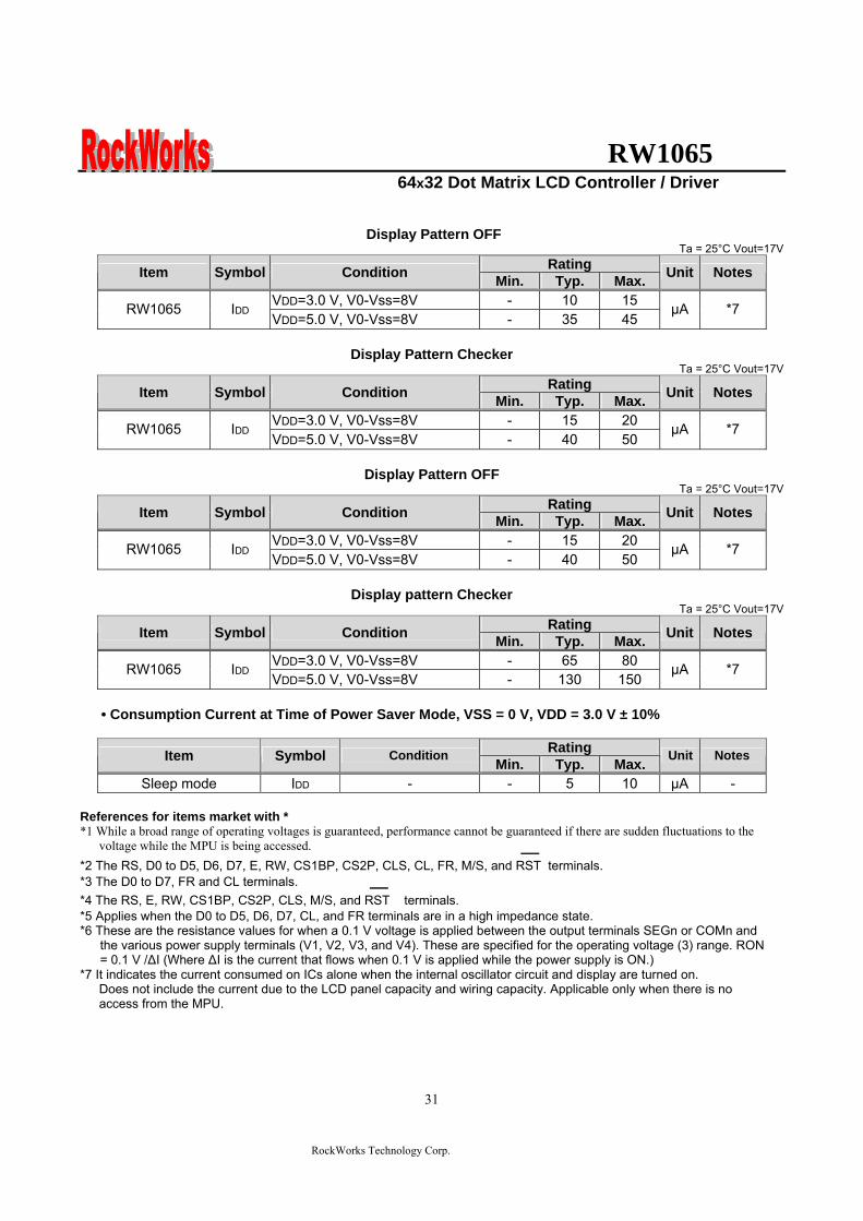
RW1065 64x32 Dot Matrix LCD Controller Driver
RockWorks Technology Corp
31
Display Pattern OFF
Ta = 25degC Vout=17V Rating Item Symbol Condition Min Typ Max Unit Notes
VDD=30 V V0-Vss=8V - 10 15 RW1065 IDD VDD=50 V V0-Vss=8V - 35 45
microA 7
Display Pattern Checker
Ta = 25degC Vout=17V Rating Item Symbol Condition Min Typ Max Unit Notes
VDD=30 V V0-Vss=8V - 15 20 RW1065 IDD VDD=50 V V0-Vss=8V - 40 50
microA 7
Display Pattern OFF
Ta = 25degC Vout=17V Rating Item Symbol Condition Min Typ Max Unit Notes
VDD=30 V V0-Vss=8V - 15 20 RW1065 IDD VDD=50 V V0-Vss=8V - 40 50
microA 7
Display pattern Checker
Ta = 25degC Vout=17V Rating Item Symbol Condition Min Typ Max Unit Notes
VDD=30 V V0-Vss=8V - 65 80 RW1065 IDD VDD=50 V V0-Vss=8V - 130 150
microA 7
bull Consumption Current at Time of Power Saver Mode VSS = 0 V VDD = 30 V plusmn 10
Rating Item Symbol Condition Min Typ Max Unit Notes
Sleep mode IDD - - 5 10 microA -
References for items market with 1 While a broad range of operating voltages is guaranteed performance cannot be guaranteed if there are sudden fluctuations to the
voltage while the MPU is being accessed 2 The RS D0 to D5 D6 D7 E RW CS1BP CS2P CLS CL FR MS and RST
― terminals
3 The D0 to D7 FR and CL terminals 4 The RS E RW CS1BP CS2P CLS MS and RST
― terminals
5 Applies when the D0 to D5 D6 D7 CL and FR terminals are in a high impedance state 6 These are the resistance values for when a 01 V voltage is applied between the output terminals SEGn or COMn and
the various power supply terminals (V1 V2 V3 and V4) These are specified for the operating voltage (3) range RON = 01 V ∆I (Where ∆I is the current that flows when 01 V is applied while the power supply is ON)
7 It indicates the current consumed on ICs alone when the internal oscillator circuit and display are turned on Does not include the current due to the LCD panel capacity and wiring capacity Applicable only when there is no access from the MPU
RW1065 64x32 Dot Matrix LCD Controller Driver
RockWorks Technology Corp
32
TIMING CHARACTERISTICS
68 Interface
(Ta=-40 to 85 degC) VDD=27 to 45V
Rating VDD=45 to 55V
Rating Item Signal Symbol ConditionMin Max Min Max
Units
Address hold time RS tAH6 0 mdash 0 mdash Address setup time RS tAW6
mdash 0 mdash 0 mdash
ns
System cycle time RS tCYC6 mdash 900 mdash 800 mdash ns Data setup time D0 to D7 tDS6 100 mdash 100 mdash Data hold time D0 to D7 tDH6
mdash 0 mdash 0 mdash
ns
Access time D0 to D7 tACC6 mdash 350 mdash 250
Output disable time D0 to D7 tOH6 CL = 100 pF
mdash 300 mdash 200 ns
Read tEWHR 360 mdash 300 mdash Enable H pulse time
WriteE
tEWHW mdash
360 mdash 300 mdash ns
Read tEWLR 450 mdash 400 mdash Enable L pulse time
WriteE
tEWLW mdash
450 mdash 400 mdash ns
1 All timing is specified using 20 and 80 of VDD as the reference 2 tEWLW and tEWLR are specified as the overlap between CS1BP being ldquoLrdquo (CS2P = ldquoHrdquo) and E
RW1065 64x32 Dot Matrix LCD Controller Driver
RockWorks Technology Corp
33
Reset Timing
Rating Item Signal Symbol Condition
Min Typ Max Units
Reset time mdash tR mdash mdash - 2 micros
Reset ldquoLrdquo pulse width RST tRW mdash 2 - mdash micros
1 When double chip was be used then the duty set command must be set between the tR
RW1065 64x32 Dot Matrix LCD Controller Driver
RockWorks Technology Corp
34
IO PAD CONFIGURATION
RW1065 64x32 Dot Matrix LCD Controller Driver
RockWorks Technology Corp
35
THE MPU INTERFACE (REFERENCE EXAMPLES) The RW1065 Series can be connected to 6800 Series MPUs The display area can be enlarged by using multiple RW1065 Series chips When this is done the chip select signal can be used to select the individual ICs to access
6800 Series MPUs
RW
106
5
RW1065 64x32 Dot Matrix LCD Controller Driver
RockWorks Technology Corp
36
When using external multi-level power supply for LCD driving (REFERENCE EXAMPLE)
Using a resistor divider can provide RW1065 external multi-level power supply for LCD driving
The circuit below shows a resistor divider network which can bias V0 V1 V2 V3 and V4 externally
RW1065 64x32 Dot Matrix LCD Controller Driver
RockWorks Technology Corp
37
bullWhen V0 V1 V2 V3 and V4 are biased by external power supply analog section of RW1065 should be turn off by software during LCD initialization The example in below shows the sequence to turn off analog section when external bias is used Begin of LCD initialization 1 Reset RW1065 2 SET EXT=1 (mode instruction)
RS RW DB7 DB6 DB5 DB4 DB3 DB2 DB1 DB00 0 0 0 0 0 1 1 0 1
3 SET Display Command (double command)
RS RW DB7 DB6 DB5 DB4 DB3 DB2 DB1 DB00 0 0 0 0 0 0 1 0 1 0 0 0 0 1 1 0 0 0 1
4 SET EXT=1 (mode instruction)
RS RW DB7 DB6 DB5 DB4 DB3 DB2 DB1 DB00 0 0 0 0 0 1 1 0 0
End of LCD initialization
bullBecause pins can not set LCD bias when external power supplies are used for LCD driving the bias can be set by an appropriate configuration for a resistor voltage divider networks The example is shown below
VSS
R
R
NR
R
R
RV1
RV2
RV3
RV4
V0
Bias Network Circuit Concept 15 Bias N=1 total = 5R 16 Bias N=2 total =6R 18 Bias N=4 total =8R 19 Bias N=5 total = 9R
RW1065 64x32 Dot Matrix LCD Controller Driver
RockWorks Technology Corp
38
Single chip solution for RW1065 application (REFERENCE EXAMPLE)
For a 64x32 application the duty cycle of LCD panel is 164 and the display duty of RW1065 should be set to 164 The display duty cycle can be selected by the DUTY bit in display command The diagram for 64x32 application is shown below
64 SEGx32COM LCD Panel
164 duty cycle
RW1065 DUTY=1
COM1~33
SEG1~65
RW1065 64x32 Dot Matrix LCD Controller Driver
RockWorks Technology Corp
39
Using an adjustable resistor on the main board to adjust the contrast of liquid crystal display (REFERENCE EXAMPLE)
The schematic shows an adjustable resistor on main board that can adjust voltage level of V0
RW1065 64x32 Dot Matrix LCD Controller Driver
RockWorks Technology Corp
40
Package information (Please pay close attention to the information in this section Do not hesitate to consult with our sale representative if you have any question or concern)
In order to make better bonding yield for RW1065 please follow the tips and recommendations in this section In this section few tips about COB footprint style PCB layout and wire bonding will be discussed
The drawing in below shows the PCB footprint style which we recommend for RW1065 Pads array in
curve shape is easier for Al wire bonding Besides that a real size COB footprint for RW1065 is also shown in below RW1065 COB footprint is also available in powerpcb or protel format for design reference purpose
The ratio is 11
RW1065 64x32 Dot Matrix LCD Controller Driver
RockWorks Technology Corp
41
During COB footprint design there have some tips about footprint that the PCB designer should know The angle between bonding wire and vertical line should less than 45 Otherwise the wire shorts would become very easy to happen at fours corners of the chip
The angle between bonding wire and vertical line could be reduced by expanding the distance between pads array and the chip In addition reducing length in horizon direction of pads array could minimize the angle between bonding wire and vertical line The picture in below will help to illustrate this concept From the experiences COB footprint style affects the bonding yield
Bad Wires are too close to each other
The angle between bonding wire and vertical line is greater than 45
The angle between bonding wire and vertical line is less than 45
Wires are not too close to each other
Reducing length in horizon direction of pads array could minimize the angle between bonding wire and vertical line
The angle between bonding wire and vertical line could be reduced by expanding the distance between pads array and the chip
RW1065 64x32 Dot Matrix LCD Controller Driver
RockWorks Technology Corp
42
If the gap between pads of COB footprint is filled with solder mask coating it is difficult to bond Al wire to
the pads The top solder masks layer that overlap COB footprint area should be removed
Please use 1 mils diameter Al wire for RW1065 wire bonding
1 2 3 4 5 6
A
B
C
D
654321
D
C
B
A
Title
Number RevisionSize
C
Date 29-Aug-2007 Sheet of File D公司資料99seMyDesignddb Drawn By
RW1065
COM131
COM142
COM153
COM164
COM175
COM186
COM197
COM208
COM219
COM2210
COM2311
COM2412
COM2513
COM2614
COM2715
COM2816
COM2917
COM3018
COM3119
SEG
6320
SEG
6221
SEG
6122
SEG
6023
SEG
5924
SEG
5825
SEG
5726
SEG
5627
SEG
5528
SEG
5429
SEG
5330
SEG
5231
SEG
5132
SEG
5033
SEG
4934
SEG
4835
SEG
4736
SEG
4637
SEG
4538
SEG
4439
SEG
4340
SEG
4241
SEG
4142
SEG
4043
SEG
3944
SEG
3845
SEG
3746
SEG
3647
SEG
3548
SEG
3449
SEG
3350
SEG
3251
SEG
3152
SEG
3053
SEG
2954
SEG
2855
SEG
2756
SEG
2657
SEG
2558
SEG
2459
SEG
2360
SEG
2261
SEG
2162
SEG
2063
SEG
1964
SEG
1865
SEG
1766
SEG
1667
SEG
1568
SEG
1469
SEG13 70SEG12 71SEG11 72SEG10 73SEG9 74SEG8 75SEG7 76SEG6 77SEG5 78SEG4 79SEG3 80SEG2 81SEG1 82SEG0 83ADCP 84CLL 85
VSS
86D
087
D1
88D
289
D3
90D
491
D5
92D
693
D7
94C
S1B
P95
CS2
P96
ERD
P97
AO
P(R
S)98
RW
RP
99V
DD
100
RST
P10
1C
LSP
102
FRR
103
MSP
104
BS1
P10
5B
S0P
106
SHLP
107
VD
D2
108
CA
P2N
109
CA
P2P
110
CA
P1P
111
CA
P1N
112
CA
P3P
113
VO
UT
114
V0
115
VR
AB
116
V3
117
V2
118
V4
119
V1
120
CO
M0
121
CO
M1
122
CO
M2
123
CO
M3
124
CO
M4
125
CO
M5
126
CO
M6
127
CO
M7
128
CO
M8
129
CO
M9
130
CO
M10
131
CO
M11
132
CO
M12
133
4897x1902 um
IC1
RW1065
C9CAPR4
100R0603
R30R0603
C8
CAP
C7
CAP
R2
100R0603
R1
0R0603C6 22uf
R50R
R6300R
R7RES1
R8NC R9
100R0603
VDD
R10
NC
R11
100R0603
R12
100R0603
R13
NC
R14
100R0603
R15
NC
VDD
D0
D1
D2
D3
D4
D5
D6
D7
DB[07]
VDDC5
01uf0603
VD
D
CS2
P
123456789
1011121314151617181920
J1
CON20
C1201uf0603
R3951K0603
VDD
CAP Value1UF~22UF
2XPut C6C8 Short R1R3Open R2R4C7C93XPut C6C8C9 R4Short R1Open R2R3C74XOpen R1R3
BS0 BS1 Bias0 0
0 1
1 0
11
15 bias
16 bias
18 bias
19 bias
ADC=0 SEG0lt~column address 00Hnormal(default) ADC=1 SEG0lt~column address 3FHinverted
SHL=0 Normal COM0~gtCOM63(default)SHL=1 Reverse direction COM63~gtCOM0
R16100R0603
LCD PANEL 64X32RockWorks
RW1065 64X32
COM0-31 SEG0-63SHL=0 ADC=0
SHL=1COM31-0
ADC=1SEG63-0
if use single chip for 32 command displaythe display command must select 164 dutyDisplay panel must select 164 duty type
VO
UT
C3P
C1N
C1P
C2P
C2N
VDD2
ADC
SHL
BS0
BS1
CLLADC
V1
V2
V3
V4
VR
AB
V0
VO
UT
C3P
C1N
C1P
C2P
C2N
VD
D2
SHL
BS0
BS1
FRR
RST
P
RW
RS
E CS1
B
CS1
V0RSRWED0D1D2D3D4D5D6D7
RSTPAK
C4
22uf
RBRES1
RA1RES1
C2
22uf
C1
22uf
C3
22uf
C0
22uf
R20
100k0603
R21
100k0603
R17
200K0603
V1
V2
V3
V4 VRAB
V0
V0
OPTION
B
R18
300R0603
RA2RES1
VADJ
R19100R
R23 RES1R22 0R
R24
RES1
R25
0R
VDD
CS1BP
CS2P
CS1
CS1
R26
22R0603
R27
22R0603
C1047uf
C11
01uf
VSS_INVDD_IN
D1DIODE
FGND
鐵框地
VSS
VDD
R28 10RR29 10RR30 10RR31 10RR32 10RR33 10RR34 10RR35 10RR36 10RR37 10RR38 10R
VADJ
1 2 3 4 5 6
A
B
C
D
654321
D
C
B
A
Title
Number RevisionSize
C
Date 29-Aug-2007 Sheet of File D公司資料99seMyDesignddb Drawn By
RW1065
COM131
COM142
COM153
COM164
COM175
COM186
COM197
COM208
COM219
COM2210
COM2311
COM2412
COM2513
COM2614
COM2715
COM2816
COM2917
COM3018
COM3119
SEG
6320
SEG
6221
SEG
6122
SEG
6023
SEG
5924
SEG
5825
SEG
5726
SEG
5627
SEG
5528
SEG
5429
SEG
5330
SEG
5231
SEG
5132
SEG
5033
SEG
4934
SEG
4835
SEG
4736
SEG
4637
SEG
4538
SEG
4439
SEG
4340
SEG
4241
SEG
4142
SEG
4043
SEG
3944
SEG
3845
SEG
3746
SEG
3647
SEG
3548
SEG
3449
SEG
3350
SEG
3251
SEG
3152
SEG
3053
SEG
2954
SEG
2855
SEG
2756
SEG
2657
SEG
2558
SEG
2459
SEG
2360
SEG
2261
SEG
2162
SEG
2063
SEG
1964
SEG
1865
SEG
1766
SEG
1667
SEG
1568
SEG
1469
SEG13 70SEG12 71SEG11 72SEG10 73SEG9 74SEG8 75SEG7 76SEG6 77SEG5 78SEG4 79SEG3 80SEG2 81SEG1 82SEG0 83ADCP 84CLL 85
VSS
86D
087
D1
88D
289
D3
90D
491
D5
92D
693
D7
94C
S1B
P95
CS2
P96
ERD
P97
AO
P(R
S)98
RW
RP
99V
DD
100
RST
P10
1C
LSP
102
FRR
103
MSP
104
BS1
P10
5B
S0P
106
SHLP
107
VD
D2
108
CA
P2N
109
CA
P2P
110
CA
P1P
111
CA
P1N
112
CA
P3P
113
VO
UT
114
V0
115
VR
AB
116
V3
117
V2
118
V4
119
V1
120
CO
M0
121
CO
M1
122
CO
M2
123
CO
M3
124
CO
M4
125
CO
M5
126
CO
M6
127
CO
M7
128
CO
M8
129
CO
M9
130
CO
M10
131
CO
M11
132
CO
M12
133
4897x1902 um
IC1
RW1065 Master
RW1065
COM131
COM142
COM153
COM164
COM175
COM186
COM197
COM208
COM219
COM2210
COM2311
COM2412
COM2513
COM2614
COM2715
COM2816
COM2917
COM3018
COM3119
SEG
6320
SEG
6221
SEG
6122
SEG
6023
SEG
5924
SEG
5825
SEG
5726
SEG
5627
SEG
5528
SEG
5429
SEG
5330
SEG
5231
SEG
5132
SEG
5033
SEG
4934
SEG
4835
SEG
4736
SEG
4637
SEG
4538
SEG
4439
SEG
4340
SEG
4241
SEG
4142
SEG
4043
SEG
3944
SEG
3845
SEG
3746
SEG
3647
SEG
3548
SEG
3449
SEG
3350
SEG
3251
SEG
3152
SEG
3053
SEG
2954
SEG
2855
SEG
2756
SEG
2657
SEG
2558
SEG
2459
SEG
2360
SEG
2261
SEG
2162
SEG
2063
SEG
1964
SEG
1865
SEG
1766
SEG
1667
SEG
1568
SEG
1469
SEG13 70SEG12 71SEG11 72SEG10 73SEG9 74SEG8 75SEG7 76SEG6 77SEG5 78SEG4 79SEG3 80SEG2 81SEG1 82SEG0 83ADCP 84CLL 85
VSS
86D
087
D1
88D
289
D3
90D
491
D5
92D
693
D7
94C
S1B
P95
CS2
P96
ERD
P97
AO
P(R
S)98
RW
RP
99V
DD
100
RST
P10
1C
LSP
102
FRR
103
MSP
104
BS1
P10
5B
S0P
106
SHLP
107
VD
D2
108
CA
P2N
109
CA
P2P
110
CA
P1P
111
CA
P1N
112
CA
P3P
113
VO
UT
114
V0
115
VR
AB
116
V3
117
V2
118
V4
119
V1
120
CO
M0
121
CO
M1
122
CO
M2
123
CO
M3
124
CO
M4
125
CO
M5
126
CO
M6
127
CO
M7
128
CO
M8
129
CO
M9
130
CO
M10
131
CO
M11
132
CO
M12
133
4897x1902 um
IC2
RW1065 Slave
C4
22uf
RBRES1
RA1RES1
C2
22uf
C1
22uf
C3
22uf
C0
22ufC9CAPR4
100R0603
R30R0603
C8
CAP
C7
CAP
R2
100R0603
R1
0R0603C6 22uf
R50R0603
R6300R0603
R7RES1
R8NC R9
100R0603
VDD
R10
NC
R11
100R0603
R12
NC
R13
100R0603
R14
100R0603
R15
NC
R16
100R0603
R17
NC
VDD
D0
D1
D2
D3
D4
D5
D6
D7
D0
D1
D2
D3
D4
D5
D6
D7
DB[07] DB[07]
VDDC10
01uf0603
VD
D
IC1_
CS2
P
VDD
IC2_
CS2
P
VD
D
C11
01uf0603
VSS
VSS
LCD PANEL 128X64
Master COM0-31 Slave COM32-63
Master SEG0-63 Slave SEG64-127
123456789
1011121314151617181920
J1
CON20
Master Slave
CAP Value1UF~22UF
2XPut C6C8 Short R1R3Open R2R4C7C93XPut C6C8C9 R4Short R1Open R2R3C74XOpen R1R3
RockWorksRW1065 128x64
BS0 BS1 Bias0 0
0 1
1 0
11
15 bias
16 bias
18 bias
19 bias
ADC=0 SEG0lt~column address 00Hnormal(default) ADC=1 SEG0lt~column address 3FHinverted
SHL=0 Normal COM0~gtCOM63(default)SHL=1 Reverse direction COM63~gtCOM0Both Master and Slave should set identical SHL value
SHL=0 SHL=0
ADC=0 ADC=0
Slave COM31-0
Slave SEG127-64
SHL=1
ADC=1
SHL=1Master COM63-32
ADC=1Master SEG63-0
R18100R0603
R22
100k0603
R23
100k0603
C501uF0603
R4551K0603
VDD
R19
200K0603
ADC1
ADC2
SHL
BS0
BS1
VDD2
V1
V2
V3
V4 VRAB
V0
V0V
OU
T
C3P
C1N
C1P
C2P
C2N
V1
V2
V3
V4
VR
AB
V0
VO
UT
C3P
C1N
C1P
C2P
C2N
VD
D2
SHL
BS0
BS1
FRR
RST
P
RW
RS
E IC1_
CS1
BP
V1
V2
V3
V4
VR
AB
V0
VO
UT
VD
D2
SHL
BS0
BS1
FRR
RST
P
RW
RS
E IC2_
CS1
BP
CLLADC1
CLLADC2
RSTP
CS1CS2
V0RSRWED0D1D2D3D4D5D6D7
AK
OPTION
R20
300R0603
RA2RES1
VADJ
R21
100R
B
R25 RESR24 0R
R26 RES R27 0RVDD
IC1_CS1BP
IC1_CS2P
CS1
CS1
R28 0R R29 RES
R30 RES R31 0R
IC2_CS1BP
IC2_CS2P
CS2
CS2
R32
22R0603
R33
22R0603
C1001uf
C11
47uf
D1DIODE
FGND
鐵框地
VSS
VDD
R34 10RR35 10RR36 10RR37 10RR38 10RR39 10RR40 10RR41 10RR42 10RR43 10RR44 10R
VSS_INVDD_IN
VADJ
VDD
1 2 3 4 5 6 7 8
A
B
C
D
87654321
D
C
B
A
Title
Number RevisionSize
D
Date 29-Aug-2007 Sheet of File D公司資料 99seMyDesignddb Drawn By
C422uf
RBRES1
RA1RES1
C3
22uf
C2
22uf
C1
22uf
C0
22ufC9CAPR4
100R0603
R30R0603
C8
CAP
C7
CAP
R2
100R0603
R1
0R0603C6 22uf
R220R0603
R23300R0603
R24RES1
R39
NCR40
100 ohm0603
VDD
R41
NC
R42
100 ohm0603
R43
NC
R44
100 ohm0603
R45
NC
R46
100 ohm0603
R47
100 ohm0603
R48
NC
R49
100 ohm0603
R50
NC
VDDCAP Value1UF~22UF
2XPut C6C8 Short R1R3Open R2R4C7C93XPut C6C8C9 R4Short R1Open R2R3C74XOpen R1R3
BS0 BS1 Bias0 0
0 1
1 0
11
15 bias
16 bias
18 bias
19 bias
ADC=0 SEG0lt~column address 00Hnormal(default)
ADC=1 SEG0lt~column address 3FHinverted
SHL=0 Normal COM0~gtCOM63(default)SHL=1 Reverse direction COM63~gtCOM0Both Master and Slave should set identical SHL value
R7
100k0603
R8
100k0603
V1
V2
V3
V4
V0
VRAB
V0
R5
200K
VDD2
VO
UT
C3P
C1N
C1P
C2P
C2N
ADC1
ADC2
ADC3
SHL
BS0
BS1
CS1CS2CS3
V0RSRWED0D1D2D3D4D5D6D7
RSTP
R3851K0603
C5
01uF
VDD
OPTION
R6
300R0603R9100R
RA2RES1
VADJ
RW1065
COM131
COM142
COM153
COM164
COM175
COM186
COM197
COM208
COM219
COM2210
COM2311
COM2412
COM2513
COM2614
COM2715
COM2816
COM2917
COM3018
COM3119
SEG
6320
SEG
6221
SEG
6122
SEG
6023
SEG
5924
SEG
5825
SEG
5726
SEG
5627
SEG
5528
SEG
5429
SEG
5330
SEG
5231
SEG
5132
SEG
5033
SEG
4934
SEG
4835
SEG
4736
SEG
4637
SEG
4538
SEG
4439
SEG
4340
SEG
4241
SEG
4142
SEG
4043
SEG
3944
SEG
3845
SEG
3746
SEG
3647
SEG
3548
SEG
3449
SEG
3350
SEG
3251
SEG
3152
SEG
3053
SEG
2954
SEG
2855
SEG
2756
SEG
2657
SEG
2558
SEG
2459
SEG
2360
SEG
2261
SEG
2162
SEG
2063
SEG
1964
SEG
1865
SEG
1766
SEG
1667
SEG
1568
SEG
1469
SEG13 70SEG12 71SEG11 72SEG10 73SEG9 74SEG8 75SEG7 76SEG6 77SEG5 78SEG4 79SEG3 80SEG2 81SEG1 82SEG0 83ADCP 84CLL 85
VSS
86D
087
D1
88D
289
D3
90D
491
D5
92D
693
D7
94C
S1B
P95
CS2
P96
ERD
P97
AO
P(R
S)98
RW
RP
99V
DD
100
RST
P10
1C
LSP
102
FRR
103
MSP
104
BS1
P10
5B
S0P
106
SHLP
107
VD
D2
108
CA
P2N
109
CA
P2P
110
CA
P1P
111
CA
P1N
112
CA
P3P
113
VO
UT
114
V0
115
VR
AB
116
V3
117
V2
118
V4
119
V1
120
CO
M0
121
CO
M1
122
CO
M2
123
CO
M3
124
CO
M4
125
CO
M5
126
CO
M6
127
CO
M7
128
CO
M8
129
CO
M9
130
CO
M10
131
CO
M11
132
CO
M12
133
4897x1902 um
IC1
RW1065 Master
RW1065
COM131
COM142
COM153
COM164
COM175
COM186
COM197
COM208
COM219
COM2210
COM2311
COM2412
COM2513
COM2614
COM2715
COM2816
COM2917
COM3018
COM3119
SEG
6320
SEG
6221
SEG
6122
SEG
6023
SEG
5924
SEG
5825
SEG
5726
SEG
5627
SEG
5528
SEG
5429
SEG
5330
SEG
5231
SEG
5132
SEG
5033
SEG
4934
SEG
4835
SEG
4736
SEG
4637
SEG
4538
SEG
4439
SEG
4340
SEG
4241
SEG
4142
SEG
4043
SEG
3944
SEG
3845
SEG
3746
SEG
3647
SEG
3548
SEG
3449
SEG
3350
SEG
3251
SEG
3152
SEG
3053
SEG
2954
SEG
2855
SEG
2756
SEG
2657
SEG
2558
SEG
2459
SEG
2360
SEG
2261
SEG
2162
SEG
2063
SEG
1964
SEG
1865
SEG
1766
SEG
1667
SEG
1568
SEG
1469
SEG13 70SEG12 71SEG11 72SEG10 73SEG9 74SEG8 75SEG7 76SEG6 77SEG5 78SEG4 79SEG3 80SEG2 81SEG1 82SEG0 83ADCP 84CLL 85
VSS
86D
087
D1
88D
289
D3
90D
491
D5
92D
693
D7
94C
S1B
P95
CS2
P96
ERD
P97
AO
P(R
S)98
RW
RP
99V
DD
100
RST
P10
1C
LSP
102
FRR
103
MSP
104
BS1
P10
5B
S0P
106
SHLP
107
VD
D2
108
CA
P2N
109
CA
P2P
110
CA
P1P
111
CA
P1N
112
CA
P3P
113
VO
UT
114
V0
115
VR
AB
116
V3
117
V2
118
V4
119
V1
120
CO
M0
121
CO
M1
122
CO
M2
123
CO
M3
124
CO
M4
125
CO
M5
126
CO
M6
127
CO
M7
128
CO
M8
129
CO
M9
130
CO
M10
131
CO
M11
132
CO
M12
133
4897x1902 um
IC2
RW1065 Slave
D0
D1
D2
D3
D4
D5
D6
D7
D0
D1
D2
D3
D4
D5
D6
D7
DB[07] DB[07]
VDDC8
01uf0603
VD
D
VDD
VD
D
C9
01uf0603
VSS
VSS
LCD PANEL 192X64
Master COM0-31 Slave COM32-63
Master SEG0-63 Slave SEG64-127
Master Slave
RockWorksRW1065 192x64
RW1065
COM131
COM142
COM153
COM164
COM175
COM186
COM197
COM208
COM219
COM2210
COM2311
COM2412
COM2513
COM2614
COM2715
COM2816
COM2917
COM3018
COM3119
SEG
6320
SEG
6221
SEG
6122
SEG
6023
SEG
5924
SEG
5825
SEG
5726
SEG
5627
SEG
5528
SEG
5429
SEG
5330
SEG
5231
SEG
5132
SEG
5033
SEG
4934
SEG
4835
SEG
4736
SEG
4637
SEG
4538
SEG
4439
SEG
4340
SEG
4241
SEG
4142
SEG
4043
SEG
3944
SEG
3845
SEG
3746
SEG
3647
SEG
3548
SEG
3449
SEG
3350
SEG
3251
SEG
3152
SEG
3053
SEG
2954
SEG
2855
SEG
2756
SEG
2657
SEG
2558
SEG
2459
SEG
2360
SEG
2261
SEG
2162
SEG
2063
SEG
1964
SEG
1865
SEG
1766
SEG
1667
SEG
1568
SEG
1469
SEG13 70SEG12 71SEG11 72SEG10 73SEG9 74SEG8 75SEG7 76SEG6 77SEG5 78SEG4 79SEG3 80SEG2 81SEG1 82SEG0 83ADCP 84CLL 85
VSS
86D
087
D1
88D
289
D3
90D
491
D5
92D
693
D7
94C
S1B
P95
CS2
P96
ERD
P97
AO
P(R
S)98
RW
RP
99V
DD
100
RST
P10
1C
LSP
102
FRR
103
MSP
104
BS1
P10
5B
S0P
106
SHLP
107
VD
D2
108
CA
P2N
109
CA
P2P
110
CA
P1P
111
CA
P1N
112
CA
P3P
113
VO
UT
114
V0
115
VR
AB
116
V3
117
V2
118
V4
119
V1
120
CO
M0
121
CO
M1
122
CO
M2
123
CO
M3
124
CO
M4
125
CO
M5
126
CO
M6
127
CO
M7
128
CO
M8
129
CO
M9
130
CO
M10
131
CO
M11
132
CO
M12
133
4897x1902 um
IC3
RW1065 Slave
D0
D1
D2
D3
D4
D5
D6
D7
DB[07]
VSS
VSS
VDD
VD
D
C10
01uf0603
Slave SEG128-192
Slave
SHL=0 SHL=0
Master COM63-32SHL=1 SHL=1
Slave COM31-0ADC=0 ADC=0 ADC=0
ADC=1 ADC=1 ADC=1Master SEG63-0 Slave SEG127-64 Slave SEG192-128
R50100R0603
V1
V2
V3
V4
VR
AB
V0
VO
UT
C3P
C1N
C1P
C2P
C2N
VD
D2
SHL
BS0
BS1
FRR
RST
P
RW
RS
E V1
V2
V3
V4
VR
AB
V0
VO
UT
VD
D2
SHL
BS0
BS1
FRR
RST
P
RW
RS
E V1
V2
V3
V4
VR
AB
V0
VO
UT
VD
D2
SHL
BS0
BS1
FRR
RST
P
RW
RS
E
CLL CLL CLLADC1 ADC2 ADC3
R25 10RR26 10RR27 10RR28 10RR29 10RR30 10RR31 10RR32 10RR33 10RR34 10RR35 10R
R36
22R0603
D1DIODE
R3722R0603
C647uf
C701uf
VSS_INVDD_IN
VSS
VDD
VADJ
123456789
101112131415161718192021222324
J1
CON24
AK
FGND
鐵框地
IC1_
CS1
BP
IC1_
CS2
P
IC2_
CS2
PIC
2_C
S1B
P
IC3_
CS1
BP
IC3_
CS2
B
R10 0R R11 RES
R12 RES R13 0RVDD
IC1_CS2B
IC1_CS1BPCS1
CS1
R14 0R R15 RES
R16 RES R17 0RVDDIC2_CS2B
IC2_CS1BPCS2
CS2
R18 0R R19 RES
R20 RES R21 0RVDDIC3_CS2B
IC3_CS1BPCS3
CS3
B
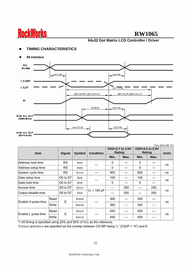
RW1065 64x32 Dot Matrix LCD Controller Driver
RockWorks Technology Corp
32
TIMING CHARACTERISTICS
68 Interface
(Ta=-40 to 85 degC) VDD=27 to 45V
Rating VDD=45 to 55V
Rating Item Signal Symbol ConditionMin Max Min Max
Units
Address hold time RS tAH6 0 mdash 0 mdash Address setup time RS tAW6
mdash 0 mdash 0 mdash
ns
System cycle time RS tCYC6 mdash 900 mdash 800 mdash ns Data setup time D0 to D7 tDS6 100 mdash 100 mdash Data hold time D0 to D7 tDH6
mdash 0 mdash 0 mdash
ns
Access time D0 to D7 tACC6 mdash 350 mdash 250
Output disable time D0 to D7 tOH6 CL = 100 pF
mdash 300 mdash 200 ns
Read tEWHR 360 mdash 300 mdash Enable H pulse time
WriteE
tEWHW mdash
360 mdash 300 mdash ns
Read tEWLR 450 mdash 400 mdash Enable L pulse time
WriteE
tEWLW mdash
450 mdash 400 mdash ns
1 All timing is specified using 20 and 80 of VDD as the reference 2 tEWLW and tEWLR are specified as the overlap between CS1BP being ldquoLrdquo (CS2P = ldquoHrdquo) and E
RW1065 64x32 Dot Matrix LCD Controller Driver
RockWorks Technology Corp
33
Reset Timing
Rating Item Signal Symbol Condition
Min Typ Max Units
Reset time mdash tR mdash mdash - 2 micros
Reset ldquoLrdquo pulse width RST tRW mdash 2 - mdash micros
1 When double chip was be used then the duty set command must be set between the tR
RW1065 64x32 Dot Matrix LCD Controller Driver
RockWorks Technology Corp
34
IO PAD CONFIGURATION
RW1065 64x32 Dot Matrix LCD Controller Driver
RockWorks Technology Corp
35
THE MPU INTERFACE (REFERENCE EXAMPLES) The RW1065 Series can be connected to 6800 Series MPUs The display area can be enlarged by using multiple RW1065 Series chips When this is done the chip select signal can be used to select the individual ICs to access
6800 Series MPUs
RW
106
5
RW1065 64x32 Dot Matrix LCD Controller Driver
RockWorks Technology Corp
36
When using external multi-level power supply for LCD driving (REFERENCE EXAMPLE)
Using a resistor divider can provide RW1065 external multi-level power supply for LCD driving
The circuit below shows a resistor divider network which can bias V0 V1 V2 V3 and V4 externally
RW1065 64x32 Dot Matrix LCD Controller Driver
RockWorks Technology Corp
37
bullWhen V0 V1 V2 V3 and V4 are biased by external power supply analog section of RW1065 should be turn off by software during LCD initialization The example in below shows the sequence to turn off analog section when external bias is used Begin of LCD initialization 1 Reset RW1065 2 SET EXT=1 (mode instruction)
RS RW DB7 DB6 DB5 DB4 DB3 DB2 DB1 DB00 0 0 0 0 0 1 1 0 1
3 SET Display Command (double command)
RS RW DB7 DB6 DB5 DB4 DB3 DB2 DB1 DB00 0 0 0 0 0 0 1 0 1 0 0 0 0 1 1 0 0 0 1
4 SET EXT=1 (mode instruction)
RS RW DB7 DB6 DB5 DB4 DB3 DB2 DB1 DB00 0 0 0 0 0 1 1 0 0
End of LCD initialization
bullBecause pins can not set LCD bias when external power supplies are used for LCD driving the bias can be set by an appropriate configuration for a resistor voltage divider networks The example is shown below
VSS
R
R
NR
R
R
RV1
RV2
RV3
RV4
V0
Bias Network Circuit Concept 15 Bias N=1 total = 5R 16 Bias N=2 total =6R 18 Bias N=4 total =8R 19 Bias N=5 total = 9R
RW1065 64x32 Dot Matrix LCD Controller Driver
RockWorks Technology Corp
38
Single chip solution for RW1065 application (REFERENCE EXAMPLE)
For a 64x32 application the duty cycle of LCD panel is 164 and the display duty of RW1065 should be set to 164 The display duty cycle can be selected by the DUTY bit in display command The diagram for 64x32 application is shown below
64 SEGx32COM LCD Panel
164 duty cycle
RW1065 DUTY=1
COM1~33
SEG1~65
RW1065 64x32 Dot Matrix LCD Controller Driver
RockWorks Technology Corp
39
Using an adjustable resistor on the main board to adjust the contrast of liquid crystal display (REFERENCE EXAMPLE)
The schematic shows an adjustable resistor on main board that can adjust voltage level of V0
RW1065 64x32 Dot Matrix LCD Controller Driver
RockWorks Technology Corp
40
Package information (Please pay close attention to the information in this section Do not hesitate to consult with our sale representative if you have any question or concern)
In order to make better bonding yield for RW1065 please follow the tips and recommendations in this section In this section few tips about COB footprint style PCB layout and wire bonding will be discussed
The drawing in below shows the PCB footprint style which we recommend for RW1065 Pads array in
curve shape is easier for Al wire bonding Besides that a real size COB footprint for RW1065 is also shown in below RW1065 COB footprint is also available in powerpcb or protel format for design reference purpose
The ratio is 11
RW1065 64x32 Dot Matrix LCD Controller Driver
RockWorks Technology Corp
41
During COB footprint design there have some tips about footprint that the PCB designer should know The angle between bonding wire and vertical line should less than 45 Otherwise the wire shorts would become very easy to happen at fours corners of the chip
The angle between bonding wire and vertical line could be reduced by expanding the distance between pads array and the chip In addition reducing length in horizon direction of pads array could minimize the angle between bonding wire and vertical line The picture in below will help to illustrate this concept From the experiences COB footprint style affects the bonding yield
Bad Wires are too close to each other
The angle between bonding wire and vertical line is greater than 45
The angle between bonding wire and vertical line is less than 45
Wires are not too close to each other
Reducing length in horizon direction of pads array could minimize the angle between bonding wire and vertical line
The angle between bonding wire and vertical line could be reduced by expanding the distance between pads array and the chip
RW1065 64x32 Dot Matrix LCD Controller Driver
RockWorks Technology Corp
42
If the gap between pads of COB footprint is filled with solder mask coating it is difficult to bond Al wire to
the pads The top solder masks layer that overlap COB footprint area should be removed
Please use 1 mils diameter Al wire for RW1065 wire bonding
1 2 3 4 5 6
A
B
C
D
654321
D
C
B
A
Title
Number RevisionSize
C
Date 29-Aug-2007 Sheet of File D公司資料99seMyDesignddb Drawn By
RW1065
COM131
COM142
COM153
COM164
COM175
COM186
COM197
COM208
COM219
COM2210
COM2311
COM2412
COM2513
COM2614
COM2715
COM2816
COM2917
COM3018
COM3119
SEG
6320
SEG
6221
SEG
6122
SEG
6023
SEG
5924
SEG
5825
SEG
5726
SEG
5627
SEG
5528
SEG
5429
SEG
5330
SEG
5231
SEG
5132
SEG
5033
SEG
4934
SEG
4835
SEG
4736
SEG
4637
SEG
4538
SEG
4439
SEG
4340
SEG
4241
SEG
4142
SEG
4043
SEG
3944
SEG
3845
SEG
3746
SEG
3647
SEG
3548
SEG
3449
SEG
3350
SEG
3251
SEG
3152
SEG
3053
SEG
2954
SEG
2855
SEG
2756
SEG
2657
SEG
2558
SEG
2459
SEG
2360
SEG
2261
SEG
2162
SEG
2063
SEG
1964
SEG
1865
SEG
1766
SEG
1667
SEG
1568
SEG
1469
SEG13 70SEG12 71SEG11 72SEG10 73SEG9 74SEG8 75SEG7 76SEG6 77SEG5 78SEG4 79SEG3 80SEG2 81SEG1 82SEG0 83ADCP 84CLL 85
VSS
86D
087
D1
88D
289
D3
90D
491
D5
92D
693
D7
94C
S1B
P95
CS2
P96
ERD
P97
AO
P(R
S)98
RW
RP
99V
DD
100
RST
P10
1C
LSP
102
FRR
103
MSP
104
BS1
P10
5B
S0P
106
SHLP
107
VD
D2
108
CA
P2N
109
CA
P2P
110
CA
P1P
111
CA
P1N
112
CA
P3P
113
VO
UT
114
V0
115
VR
AB
116
V3
117
V2
118
V4
119
V1
120
CO
M0
121
CO
M1
122
CO
M2
123
CO
M3
124
CO
M4
125
CO
M5
126
CO
M6
127
CO
M7
128
CO
M8
129
CO
M9
130
CO
M10
131
CO
M11
132
CO
M12
133
4897x1902 um
IC1
RW1065
C9CAPR4
100R0603
R30R0603
C8
CAP
C7
CAP
R2
100R0603
R1
0R0603C6 22uf
R50R
R6300R
R7RES1
R8NC R9
100R0603
VDD
R10
NC
R11
100R0603
R12
100R0603
R13
NC
R14
100R0603
R15
NC
VDD
D0
D1
D2
D3
D4
D5
D6
D7
DB[07]
VDDC5
01uf0603
VD
D
CS2
P
123456789
1011121314151617181920
J1
CON20
C1201uf0603
R3951K0603
VDD
CAP Value1UF~22UF
2XPut C6C8 Short R1R3Open R2R4C7C93XPut C6C8C9 R4Short R1Open R2R3C74XOpen R1R3
BS0 BS1 Bias0 0
0 1
1 0
11
15 bias
16 bias
18 bias
19 bias
ADC=0 SEG0lt~column address 00Hnormal(default) ADC=1 SEG0lt~column address 3FHinverted
SHL=0 Normal COM0~gtCOM63(default)SHL=1 Reverse direction COM63~gtCOM0
R16100R0603
LCD PANEL 64X32RockWorks
RW1065 64X32
COM0-31 SEG0-63SHL=0 ADC=0
SHL=1COM31-0
ADC=1SEG63-0
if use single chip for 32 command displaythe display command must select 164 dutyDisplay panel must select 164 duty type
VO
UT
C3P
C1N
C1P
C2P
C2N
VDD2
ADC
SHL
BS0
BS1
CLLADC
V1
V2
V3
V4
VR
AB
V0
VO
UT
C3P
C1N
C1P
C2P
C2N
VD
D2
SHL
BS0
BS1
FRR
RST
P
RW
RS
E CS1
B
CS1
V0RSRWED0D1D2D3D4D5D6D7
RSTPAK
C4
22uf
RBRES1
RA1RES1
C2
22uf
C1
22uf
C3
22uf
C0
22uf
R20
100k0603
R21
100k0603
R17
200K0603
V1
V2
V3
V4 VRAB
V0
V0
OPTION
B
R18
300R0603
RA2RES1
VADJ
R19100R
R23 RES1R22 0R
R24
RES1
R25
0R
VDD
CS1BP
CS2P
CS1
CS1
R26
22R0603
R27
22R0603
C1047uf
C11
01uf
VSS_INVDD_IN
D1DIODE
FGND
鐵框地
VSS
VDD
R28 10RR29 10RR30 10RR31 10RR32 10RR33 10RR34 10RR35 10RR36 10RR37 10RR38 10R
VADJ
1 2 3 4 5 6
A
B
C
D
654321
D
C
B
A
Title
Number RevisionSize
C
Date 29-Aug-2007 Sheet of File D公司資料99seMyDesignddb Drawn By
RW1065
COM131
COM142
COM153
COM164
COM175
COM186
COM197
COM208
COM219
COM2210
COM2311
COM2412
COM2513
COM2614
COM2715
COM2816
COM2917
COM3018
COM3119
SEG
6320
SEG
6221
SEG
6122
SEG
6023
SEG
5924
SEG
5825
SEG
5726
SEG
5627
SEG
5528
SEG
5429
SEG
5330
SEG
5231
SEG
5132
SEG
5033
SEG
4934
SEG
4835
SEG
4736
SEG
4637
SEG
4538
SEG
4439
SEG
4340
SEG
4241
SEG
4142
SEG
4043
SEG
3944
SEG
3845
SEG
3746
SEG
3647
SEG
3548
SEG
3449
SEG
3350
SEG
3251
SEG
3152
SEG
3053
SEG
2954
SEG
2855
SEG
2756
SEG
2657
SEG
2558
SEG
2459
SEG
2360
SEG
2261
SEG
2162
SEG
2063
SEG
1964
SEG
1865
SEG
1766
SEG
1667
SEG
1568
SEG
1469
SEG13 70SEG12 71SEG11 72SEG10 73SEG9 74SEG8 75SEG7 76SEG6 77SEG5 78SEG4 79SEG3 80SEG2 81SEG1 82SEG0 83ADCP 84CLL 85
VSS
86D
087
D1
88D
289
D3
90D
491
D5
92D
693
D7
94C
S1B
P95
CS2
P96
ERD
P97
AO
P(R
S)98
RW
RP
99V
DD
100
RST
P10
1C
LSP
102
FRR
103
MSP
104
BS1
P10
5B
S0P
106
SHLP
107
VD
D2
108
CA
P2N
109
CA
P2P
110
CA
P1P
111
CA
P1N
112
CA
P3P
113
VO
UT
114
V0
115
VR
AB
116
V3
117
V2
118
V4
119
V1
120
CO
M0
121
CO
M1
122
CO
M2
123
CO
M3
124
CO
M4
125
CO
M5
126
CO
M6
127
CO
M7
128
CO
M8
129
CO
M9
130
CO
M10
131
CO
M11
132
CO
M12
133
4897x1902 um
IC1
RW1065 Master
RW1065
COM131
COM142
COM153
COM164
COM175
COM186
COM197
COM208
COM219
COM2210
COM2311
COM2412
COM2513
COM2614
COM2715
COM2816
COM2917
COM3018
COM3119
SEG
6320
SEG
6221
SEG
6122
SEG
6023
SEG
5924
SEG
5825
SEG
5726
SEG
5627
SEG
5528
SEG
5429
SEG
5330
SEG
5231
SEG
5132
SEG
5033
SEG
4934
SEG
4835
SEG
4736
SEG
4637
SEG
4538
SEG
4439
SEG
4340
SEG
4241
SEG
4142
SEG
4043
SEG
3944
SEG
3845
SEG
3746
SEG
3647
SEG
3548
SEG
3449
SEG
3350
SEG
3251
SEG
3152
SEG
3053
SEG
2954
SEG
2855
SEG
2756
SEG
2657
SEG
2558
SEG
2459
SEG
2360
SEG
2261
SEG
2162
SEG
2063
SEG
1964
SEG
1865
SEG
1766
SEG
1667
SEG
1568
SEG
1469
SEG13 70SEG12 71SEG11 72SEG10 73SEG9 74SEG8 75SEG7 76SEG6 77SEG5 78SEG4 79SEG3 80SEG2 81SEG1 82SEG0 83ADCP 84CLL 85
VSS
86D
087
D1
88D
289
D3
90D
491
D5
92D
693
D7
94C
S1B
P95
CS2
P96
ERD
P97
AO
P(R
S)98
RW
RP
99V
DD
100
RST
P10
1C
LSP
102
FRR
103
MSP
104
BS1
P10
5B
S0P
106
SHLP
107
VD
D2
108
CA
P2N
109
CA
P2P
110
CA
P1P
111
CA
P1N
112
CA
P3P
113
VO
UT
114
V0
115
VR
AB
116
V3
117
V2
118
V4
119
V1
120
CO
M0
121
CO
M1
122
CO
M2
123
CO
M3
124
CO
M4
125
CO
M5
126
CO
M6
127
CO
M7
128
CO
M8
129
CO
M9
130
CO
M10
131
CO
M11
132
CO
M12
133
4897x1902 um
IC2
RW1065 Slave
C4
22uf
RBRES1
RA1RES1
C2
22uf
C1
22uf
C3
22uf
C0
22ufC9CAPR4
100R0603
R30R0603
C8
CAP
C7
CAP
R2
100R0603
R1
0R0603C6 22uf
R50R0603
R6300R0603
R7RES1
R8NC R9
100R0603
VDD
R10
NC
R11
100R0603
R12
NC
R13
100R0603
R14
100R0603
R15
NC
R16
100R0603
R17
NC
VDD
D0
D1
D2
D3
D4
D5
D6
D7
D0
D1
D2
D3
D4
D5
D6
D7
DB[07] DB[07]
VDDC10
01uf0603
VD
D
IC1_
CS2
P
VDD
IC2_
CS2
P
VD
D
C11
01uf0603
VSS
VSS
LCD PANEL 128X64
Master COM0-31 Slave COM32-63
Master SEG0-63 Slave SEG64-127
123456789
1011121314151617181920
J1
CON20
Master Slave
CAP Value1UF~22UF
2XPut C6C8 Short R1R3Open R2R4C7C93XPut C6C8C9 R4Short R1Open R2R3C74XOpen R1R3
RockWorksRW1065 128x64
BS0 BS1 Bias0 0
0 1
1 0
11
15 bias
16 bias
18 bias
19 bias
ADC=0 SEG0lt~column address 00Hnormal(default) ADC=1 SEG0lt~column address 3FHinverted
SHL=0 Normal COM0~gtCOM63(default)SHL=1 Reverse direction COM63~gtCOM0Both Master and Slave should set identical SHL value
SHL=0 SHL=0
ADC=0 ADC=0
Slave COM31-0
Slave SEG127-64
SHL=1
ADC=1
SHL=1Master COM63-32
ADC=1Master SEG63-0
R18100R0603
R22
100k0603
R23
100k0603
C501uF0603
R4551K0603
VDD
R19
200K0603
ADC1
ADC2
SHL
BS0
BS1
VDD2
V1
V2
V3
V4 VRAB
V0
V0V
OU
T
C3P
C1N
C1P
C2P
C2N
V1
V2
V3
V4
VR
AB
V0
VO
UT
C3P
C1N
C1P
C2P
C2N
VD
D2
SHL
BS0
BS1
FRR
RST
P
RW
RS
E IC1_
CS1
BP
V1
V2
V3
V4
VR
AB
V0
VO
UT
VD
D2
SHL
BS0
BS1
FRR
RST
P
RW
RS
E IC2_
CS1
BP
CLLADC1
CLLADC2
RSTP
CS1CS2
V0RSRWED0D1D2D3D4D5D6D7
AK
OPTION
R20
300R0603
RA2RES1
VADJ
R21
100R
B
R25 RESR24 0R
R26 RES R27 0RVDD
IC1_CS1BP
IC1_CS2P
CS1
CS1
R28 0R R29 RES
R30 RES R31 0R
IC2_CS1BP
IC2_CS2P
CS2
CS2
R32
22R0603
R33
22R0603
C1001uf
C11
47uf
D1DIODE
FGND
鐵框地
VSS
VDD
R34 10RR35 10RR36 10RR37 10RR38 10RR39 10RR40 10RR41 10RR42 10RR43 10RR44 10R
VSS_INVDD_IN
VADJ
VDD
1 2 3 4 5 6 7 8
A
B
C
D
87654321
D
C
B
A
Title
Number RevisionSize
D
Date 29-Aug-2007 Sheet of File D公司資料 99seMyDesignddb Drawn By
C422uf
RBRES1
RA1RES1
C3
22uf
C2
22uf
C1
22uf
C0
22ufC9CAPR4
100R0603
R30R0603
C8
CAP
C7
CAP
R2
100R0603
R1
0R0603C6 22uf
R220R0603
R23300R0603
R24RES1
R39
NCR40
100 ohm0603
VDD
R41
NC
R42
100 ohm0603
R43
NC
R44
100 ohm0603
R45
NC
R46
100 ohm0603
R47
100 ohm0603
R48
NC
R49
100 ohm0603
R50
NC
VDDCAP Value1UF~22UF
2XPut C6C8 Short R1R3Open R2R4C7C93XPut C6C8C9 R4Short R1Open R2R3C74XOpen R1R3
BS0 BS1 Bias0 0
0 1
1 0
11
15 bias
16 bias
18 bias
19 bias
ADC=0 SEG0lt~column address 00Hnormal(default)
ADC=1 SEG0lt~column address 3FHinverted
SHL=0 Normal COM0~gtCOM63(default)SHL=1 Reverse direction COM63~gtCOM0Both Master and Slave should set identical SHL value
R7
100k0603
R8
100k0603
V1
V2
V3
V4
V0
VRAB
V0
R5
200K
VDD2
VO
UT
C3P
C1N
C1P
C2P
C2N
ADC1
ADC2
ADC3
SHL
BS0
BS1
CS1CS2CS3
V0RSRWED0D1D2D3D4D5D6D7
RSTP
R3851K0603
C5
01uF
VDD
OPTION
R6
300R0603R9100R
RA2RES1
VADJ
RW1065
COM131
COM142
COM153
COM164
COM175
COM186
COM197
COM208
COM219
COM2210
COM2311
COM2412
COM2513
COM2614
COM2715
COM2816
COM2917
COM3018
COM3119
SEG
6320
SEG
6221
SEG
6122
SEG
6023
SEG
5924
SEG
5825
SEG
5726
SEG
5627
SEG
5528
SEG
5429
SEG
5330
SEG
5231
SEG
5132
SEG
5033
SEG
4934
SEG
4835
SEG
4736
SEG
4637
SEG
4538
SEG
4439
SEG
4340
SEG
4241
SEG
4142
SEG
4043
SEG
3944
SEG
3845
SEG
3746
SEG
3647
SEG
3548
SEG
3449
SEG
3350
SEG
3251
SEG
3152
SEG
3053
SEG
2954
SEG
2855
SEG
2756
SEG
2657
SEG
2558
SEG
2459
SEG
2360
SEG
2261
SEG
2162
SEG
2063
SEG
1964
SEG
1865
SEG
1766
SEG
1667
SEG
1568
SEG
1469
SEG13 70SEG12 71SEG11 72SEG10 73SEG9 74SEG8 75SEG7 76SEG6 77SEG5 78SEG4 79SEG3 80SEG2 81SEG1 82SEG0 83ADCP 84CLL 85
VSS
86D
087
D1
88D
289
D3
90D
491
D5
92D
693
D7
94C
S1B
P95
CS2
P96
ERD
P97
AO
P(R
S)98
RW
RP
99V
DD
100
RST
P10
1C
LSP
102
FRR
103
MSP
104
BS1
P10
5B
S0P
106
SHLP
107
VD
D2
108
CA
P2N
109
CA
P2P
110
CA
P1P
111
CA
P1N
112
CA
P3P
113
VO
UT
114
V0
115
VR
AB
116
V3
117
V2
118
V4
119
V1
120
CO
M0
121
CO
M1
122
CO
M2
123
CO
M3
124
CO
M4
125
CO
M5
126
CO
M6
127
CO
M7
128
CO
M8
129
CO
M9
130
CO
M10
131
CO
M11
132
CO
M12
133
4897x1902 um
IC1
RW1065 Master
RW1065
COM131
COM142
COM153
COM164
COM175
COM186
COM197
COM208
COM219
COM2210
COM2311
COM2412
COM2513
COM2614
COM2715
COM2816
COM2917
COM3018
COM3119
SEG
6320
SEG
6221
SEG
6122
SEG
6023
SEG
5924
SEG
5825
SEG
5726
SEG
5627
SEG
5528
SEG
5429
SEG
5330
SEG
5231
SEG
5132
SEG
5033
SEG
4934
SEG
4835
SEG
4736
SEG
4637
SEG
4538
SEG
4439
SEG
4340
SEG
4241
SEG
4142
SEG
4043
SEG
3944
SEG
3845
SEG
3746
SEG
3647
SEG
3548
SEG
3449
SEG
3350
SEG
3251
SEG
3152
SEG
3053
SEG
2954
SEG
2855
SEG
2756
SEG
2657
SEG
2558
SEG
2459
SEG
2360
SEG
2261
SEG
2162
SEG
2063
SEG
1964
SEG
1865
SEG
1766
SEG
1667
SEG
1568
SEG
1469
SEG13 70SEG12 71SEG11 72SEG10 73SEG9 74SEG8 75SEG7 76SEG6 77SEG5 78SEG4 79SEG3 80SEG2 81SEG1 82SEG0 83ADCP 84CLL 85
VSS
86D
087
D1
88D
289
D3
90D
491
D5
92D
693
D7
94C
S1B
P95
CS2
P96
ERD
P97
AO
P(R
S)98
RW
RP
99V
DD
100
RST
P10
1C
LSP
102
FRR
103
MSP
104
BS1
P10
5B
S0P
106
SHLP
107
VD
D2
108
CA
P2N
109
CA
P2P
110
CA
P1P
111
CA
P1N
112
CA
P3P
113
VO
UT
114
V0
115
VR
AB
116
V3
117
V2
118
V4
119
V1
120
CO
M0
121
CO
M1
122
CO
M2
123
CO
M3
124
CO
M4
125
CO
M5
126
CO
M6
127
CO
M7
128
CO
M8
129
CO
M9
130
CO
M10
131
CO
M11
132
CO
M12
133
4897x1902 um
IC2
RW1065 Slave
D0
D1
D2
D3
D4
D5
D6
D7
D0
D1
D2
D3
D4
D5
D6
D7
DB[07] DB[07]
VDDC8
01uf0603
VD
D
VDD
VD
D
C9
01uf0603
VSS
VSS
LCD PANEL 192X64
Master COM0-31 Slave COM32-63
Master SEG0-63 Slave SEG64-127
Master Slave
RockWorksRW1065 192x64
RW1065
COM131
COM142
COM153
COM164
COM175
COM186
COM197
COM208
COM219
COM2210
COM2311
COM2412
COM2513
COM2614
COM2715
COM2816
COM2917
COM3018
COM3119
SEG
6320
SEG
6221
SEG
6122
SEG
6023
SEG
5924
SEG
5825
SEG
5726
SEG
5627
SEG
5528
SEG
5429
SEG
5330
SEG
5231
SEG
5132
SEG
5033
SEG
4934
SEG
4835
SEG
4736
SEG
4637
SEG
4538
SEG
4439
SEG
4340
SEG
4241
SEG
4142
SEG
4043
SEG
3944
SEG
3845
SEG
3746
SEG
3647
SEG
3548
SEG
3449
SEG
3350
SEG
3251
SEG
3152
SEG
3053
SEG
2954
SEG
2855
SEG
2756
SEG
2657
SEG
2558
SEG
2459
SEG
2360
SEG
2261
SEG
2162
SEG
2063
SEG
1964
SEG
1865
SEG
1766
SEG
1667
SEG
1568
SEG
1469
SEG13 70SEG12 71SEG11 72SEG10 73SEG9 74SEG8 75SEG7 76SEG6 77SEG5 78SEG4 79SEG3 80SEG2 81SEG1 82SEG0 83ADCP 84CLL 85
VSS
86D
087
D1
88D
289
D3
90D
491
D5
92D
693
D7
94C
S1B
P95
CS2
P96
ERD
P97
AO
P(R
S)98
RW
RP
99V
DD
100
RST
P10
1C
LSP
102
FRR
103
MSP
104
BS1
P10
5B
S0P
106
SHLP
107
VD
D2
108
CA
P2N
109
CA
P2P
110
CA
P1P
111
CA
P1N
112
CA
P3P
113
VO
UT
114
V0
115
VR
AB
116
V3
117
V2
118
V4
119
V1
120
CO
M0
121
CO
M1
122
CO
M2
123
CO
M3
124
CO
M4
125
CO
M5
126
CO
M6
127
CO
M7
128
CO
M8
129
CO
M9
130
CO
M10
131
CO
M11
132
CO
M12
133
4897x1902 um
IC3
RW1065 Slave
D0
D1
D2
D3
D4
D5
D6
D7
DB[07]
VSS
VSS
VDD
VD
D
C10
01uf0603
Slave SEG128-192
Slave
SHL=0 SHL=0
Master COM63-32SHL=1 SHL=1
Slave COM31-0ADC=0 ADC=0 ADC=0
ADC=1 ADC=1 ADC=1Master SEG63-0 Slave SEG127-64 Slave SEG192-128
R50100R0603
V1
V2
V3
V4
VR
AB
V0
VO
UT
C3P
C1N
C1P
C2P
C2N
VD
D2
SHL
BS0
BS1
FRR
RST
P
RW
RS
E V1
V2
V3
V4
VR
AB
V0
VO
UT
VD
D2
SHL
BS0
BS1
FRR
RST
P
RW
RS
E V1
V2
V3
V4
VR
AB
V0
VO
UT
VD
D2
SHL
BS0
BS1
FRR
RST
P
RW
RS
E
CLL CLL CLLADC1 ADC2 ADC3
R25 10RR26 10RR27 10RR28 10RR29 10RR30 10RR31 10RR32 10RR33 10RR34 10RR35 10R
R36
22R0603
D1DIODE
R3722R0603
C647uf
C701uf
VSS_INVDD_IN
VSS
VDD
VADJ
123456789
101112131415161718192021222324
J1
CON24
AK
FGND
鐵框地
IC1_
CS1
BP
IC1_
CS2
P
IC2_
CS2
PIC
2_C
S1B
P
IC3_
CS1
BP
IC3_
CS2
B
R10 0R R11 RES
R12 RES R13 0RVDD
IC1_CS2B
IC1_CS1BPCS1
CS1
R14 0R R15 RES
R16 RES R17 0RVDDIC2_CS2B
IC2_CS1BPCS2
CS2
R18 0R R19 RES
R20 RES R21 0RVDDIC3_CS2B
IC3_CS1BPCS3
CS3
B
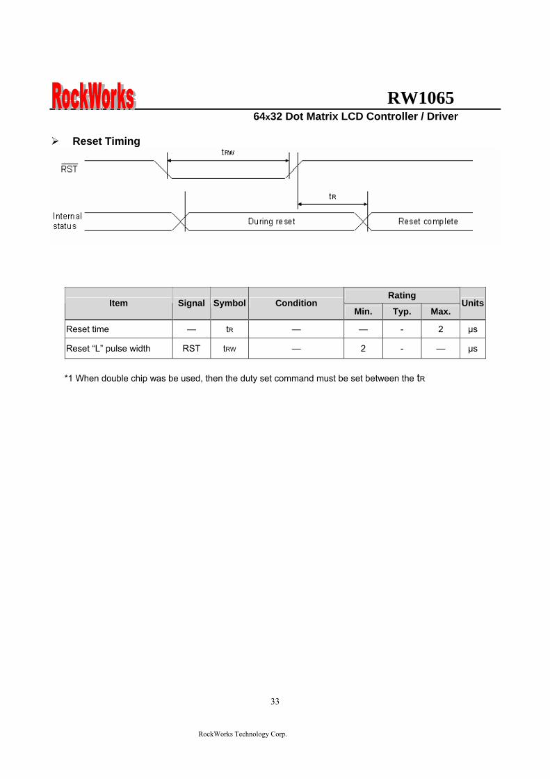
RW1065 64x32 Dot Matrix LCD Controller Driver
RockWorks Technology Corp
33
Reset Timing
Rating Item Signal Symbol Condition
Min Typ Max Units
Reset time mdash tR mdash mdash - 2 micros
Reset ldquoLrdquo pulse width RST tRW mdash 2 - mdash micros
1 When double chip was be used then the duty set command must be set between the tR
RW1065 64x32 Dot Matrix LCD Controller Driver
RockWorks Technology Corp
34
IO PAD CONFIGURATION
RW1065 64x32 Dot Matrix LCD Controller Driver
RockWorks Technology Corp
35
THE MPU INTERFACE (REFERENCE EXAMPLES) The RW1065 Series can be connected to 6800 Series MPUs The display area can be enlarged by using multiple RW1065 Series chips When this is done the chip select signal can be used to select the individual ICs to access
6800 Series MPUs
RW
106
5
RW1065 64x32 Dot Matrix LCD Controller Driver
RockWorks Technology Corp
36
When using external multi-level power supply for LCD driving (REFERENCE EXAMPLE)
Using a resistor divider can provide RW1065 external multi-level power supply for LCD driving
The circuit below shows a resistor divider network which can bias V0 V1 V2 V3 and V4 externally
RW1065 64x32 Dot Matrix LCD Controller Driver
RockWorks Technology Corp
37
bullWhen V0 V1 V2 V3 and V4 are biased by external power supply analog section of RW1065 should be turn off by software during LCD initialization The example in below shows the sequence to turn off analog section when external bias is used Begin of LCD initialization 1 Reset RW1065 2 SET EXT=1 (mode instruction)
RS RW DB7 DB6 DB5 DB4 DB3 DB2 DB1 DB00 0 0 0 0 0 1 1 0 1
3 SET Display Command (double command)
RS RW DB7 DB6 DB5 DB4 DB3 DB2 DB1 DB00 0 0 0 0 0 0 1 0 1 0 0 0 0 1 1 0 0 0 1
4 SET EXT=1 (mode instruction)
RS RW DB7 DB6 DB5 DB4 DB3 DB2 DB1 DB00 0 0 0 0 0 1 1 0 0
End of LCD initialization
bullBecause pins can not set LCD bias when external power supplies are used for LCD driving the bias can be set by an appropriate configuration for a resistor voltage divider networks The example is shown below
VSS
R
R
NR
R
R
RV1
RV2
RV3
RV4
V0
Bias Network Circuit Concept 15 Bias N=1 total = 5R 16 Bias N=2 total =6R 18 Bias N=4 total =8R 19 Bias N=5 total = 9R
RW1065 64x32 Dot Matrix LCD Controller Driver
RockWorks Technology Corp
38
Single chip solution for RW1065 application (REFERENCE EXAMPLE)
For a 64x32 application the duty cycle of LCD panel is 164 and the display duty of RW1065 should be set to 164 The display duty cycle can be selected by the DUTY bit in display command The diagram for 64x32 application is shown below
64 SEGx32COM LCD Panel
164 duty cycle
RW1065 DUTY=1
COM1~33
SEG1~65
RW1065 64x32 Dot Matrix LCD Controller Driver
RockWorks Technology Corp
39
Using an adjustable resistor on the main board to adjust the contrast of liquid crystal display (REFERENCE EXAMPLE)
The schematic shows an adjustable resistor on main board that can adjust voltage level of V0
RW1065 64x32 Dot Matrix LCD Controller Driver
RockWorks Technology Corp
40
Package information (Please pay close attention to the information in this section Do not hesitate to consult with our sale representative if you have any question or concern)
In order to make better bonding yield for RW1065 please follow the tips and recommendations in this section In this section few tips about COB footprint style PCB layout and wire bonding will be discussed
The drawing in below shows the PCB footprint style which we recommend for RW1065 Pads array in
curve shape is easier for Al wire bonding Besides that a real size COB footprint for RW1065 is also shown in below RW1065 COB footprint is also available in powerpcb or protel format for design reference purpose
The ratio is 11
RW1065 64x32 Dot Matrix LCD Controller Driver
RockWorks Technology Corp
41
During COB footprint design there have some tips about footprint that the PCB designer should know The angle between bonding wire and vertical line should less than 45 Otherwise the wire shorts would become very easy to happen at fours corners of the chip
The angle between bonding wire and vertical line could be reduced by expanding the distance between pads array and the chip In addition reducing length in horizon direction of pads array could minimize the angle between bonding wire and vertical line The picture in below will help to illustrate this concept From the experiences COB footprint style affects the bonding yield
Bad Wires are too close to each other
The angle between bonding wire and vertical line is greater than 45
The angle between bonding wire and vertical line is less than 45
Wires are not too close to each other
Reducing length in horizon direction of pads array could minimize the angle between bonding wire and vertical line
The angle between bonding wire and vertical line could be reduced by expanding the distance between pads array and the chip
RW1065 64x32 Dot Matrix LCD Controller Driver
RockWorks Technology Corp
42
If the gap between pads of COB footprint is filled with solder mask coating it is difficult to bond Al wire to
the pads The top solder masks layer that overlap COB footprint area should be removed
Please use 1 mils diameter Al wire for RW1065 wire bonding
1 2 3 4 5 6
A
B
C
D
654321
D
C
B
A
Title
Number RevisionSize
C
Date 29-Aug-2007 Sheet of File D公司資料99seMyDesignddb Drawn By
RW1065
COM131
COM142
COM153
COM164
COM175
COM186
COM197
COM208
COM219
COM2210
COM2311
COM2412
COM2513
COM2614
COM2715
COM2816
COM2917
COM3018
COM3119
SEG
6320
SEG
6221
SEG
6122
SEG
6023
SEG
5924
SEG
5825
SEG
5726
SEG
5627
SEG
5528
SEG
5429
SEG
5330
SEG
5231
SEG
5132
SEG
5033
SEG
4934
SEG
4835
SEG
4736
SEG
4637
SEG
4538
SEG
4439
SEG
4340
SEG
4241
SEG
4142
SEG
4043
SEG
3944
SEG
3845
SEG
3746
SEG
3647
SEG
3548
SEG
3449
SEG
3350
SEG
3251
SEG
3152
SEG
3053
SEG
2954
SEG
2855
SEG
2756
SEG
2657
SEG
2558
SEG
2459
SEG
2360
SEG
2261
SEG
2162
SEG
2063
SEG
1964
SEG
1865
SEG
1766
SEG
1667
SEG
1568
SEG
1469
SEG13 70SEG12 71SEG11 72SEG10 73SEG9 74SEG8 75SEG7 76SEG6 77SEG5 78SEG4 79SEG3 80SEG2 81SEG1 82SEG0 83ADCP 84CLL 85
VSS
86D
087
D1
88D
289
D3
90D
491
D5
92D
693
D7
94C
S1B
P95
CS2
P96
ERD
P97
AO
P(R
S)98
RW
RP
99V
DD
100
RST
P10
1C
LSP
102
FRR
103
MSP
104
BS1
P10
5B
S0P
106
SHLP
107
VD
D2
108
CA
P2N
109
CA
P2P
110
CA
P1P
111
CA
P1N
112
CA
P3P
113
VO
UT
114
V0
115
VR
AB
116
V3
117
V2
118
V4
119
V1
120
CO
M0
121
CO
M1
122
CO
M2
123
CO
M3
124
CO
M4
125
CO
M5
126
CO
M6
127
CO
M7
128
CO
M8
129
CO
M9
130
CO
M10
131
CO
M11
132
CO
M12
133
4897x1902 um
IC1
RW1065
C9CAPR4
100R0603
R30R0603
C8
CAP
C7
CAP
R2
100R0603
R1
0R0603C6 22uf
R50R
R6300R
R7RES1
R8NC R9
100R0603
VDD
R10
NC
R11
100R0603
R12
100R0603
R13
NC
R14
100R0603
R15
NC
VDD
D0
D1
D2
D3
D4
D5
D6
D7
DB[07]
VDDC5
01uf0603
VD
D
CS2
P
123456789
1011121314151617181920
J1
CON20
C1201uf0603
R3951K0603
VDD
CAP Value1UF~22UF
2XPut C6C8 Short R1R3Open R2R4C7C93XPut C6C8C9 R4Short R1Open R2R3C74XOpen R1R3
BS0 BS1 Bias0 0
0 1
1 0
11
15 bias
16 bias
18 bias
19 bias
ADC=0 SEG0lt~column address 00Hnormal(default) ADC=1 SEG0lt~column address 3FHinverted
SHL=0 Normal COM0~gtCOM63(default)SHL=1 Reverse direction COM63~gtCOM0
R16100R0603
LCD PANEL 64X32RockWorks
RW1065 64X32
COM0-31 SEG0-63SHL=0 ADC=0
SHL=1COM31-0
ADC=1SEG63-0
if use single chip for 32 command displaythe display command must select 164 dutyDisplay panel must select 164 duty type
VO
UT
C3P
C1N
C1P
C2P
C2N
VDD2
ADC
SHL
BS0
BS1
CLLADC
V1
V2
V3
V4
VR
AB
V0
VO
UT
C3P
C1N
C1P
C2P
C2N
VD
D2
SHL
BS0
BS1
FRR
RST
P
RW
RS
E CS1
B
CS1
V0RSRWED0D1D2D3D4D5D6D7
RSTPAK
C4
22uf
RBRES1
RA1RES1
C2
22uf
C1
22uf
C3
22uf
C0
22uf
R20
100k0603
R21
100k0603
R17
200K0603
V1
V2
V3
V4 VRAB
V0
V0
OPTION
B
R18
300R0603
RA2RES1
VADJ
R19100R
R23 RES1R22 0R
R24
RES1
R25
0R
VDD
CS1BP
CS2P
CS1
CS1
R26
22R0603
R27
22R0603
C1047uf
C11
01uf
VSS_INVDD_IN
D1DIODE
FGND
鐵框地
VSS
VDD
R28 10RR29 10RR30 10RR31 10RR32 10RR33 10RR34 10RR35 10RR36 10RR37 10RR38 10R
VADJ
1 2 3 4 5 6
A
B
C
D
654321
D
C
B
A
Title
Number RevisionSize
C
Date 29-Aug-2007 Sheet of File D公司資料99seMyDesignddb Drawn By
RW1065
COM131
COM142
COM153
COM164
COM175
COM186
COM197
COM208
COM219
COM2210
COM2311
COM2412
COM2513
COM2614
COM2715
COM2816
COM2917
COM3018
COM3119
SEG
6320
SEG
6221
SEG
6122
SEG
6023
SEG
5924
SEG
5825
SEG
5726
SEG
5627
SEG
5528
SEG
5429
SEG
5330
SEG
5231
SEG
5132
SEG
5033
SEG
4934
SEG
4835
SEG
4736
SEG
4637
SEG
4538
SEG
4439
SEG
4340
SEG
4241
SEG
4142
SEG
4043
SEG
3944
SEG
3845
SEG
3746
SEG
3647
SEG
3548
SEG
3449
SEG
3350
SEG
3251
SEG
3152
SEG
3053
SEG
2954
SEG
2855
SEG
2756
SEG
2657
SEG
2558
SEG
2459
SEG
2360
SEG
2261
SEG
2162
SEG
2063
SEG
1964
SEG
1865
SEG
1766
SEG
1667
SEG
1568
SEG
1469
SEG13 70SEG12 71SEG11 72SEG10 73SEG9 74SEG8 75SEG7 76SEG6 77SEG5 78SEG4 79SEG3 80SEG2 81SEG1 82SEG0 83ADCP 84CLL 85
VSS
86D
087
D1
88D
289
D3
90D
491
D5
92D
693
D7
94C
S1B
P95
CS2
P96
ERD
P97
AO
P(R
S)98
RW
RP
99V
DD
100
RST
P10
1C
LSP
102
FRR
103
MSP
104
BS1
P10
5B
S0P
106
SHLP
107
VD
D2
108
CA
P2N
109
CA
P2P
110
CA
P1P
111
CA
P1N
112
CA
P3P
113
VO
UT
114
V0
115
VR
AB
116
V3
117
V2
118
V4
119
V1
120
CO
M0
121
CO
M1
122
CO
M2
123
CO
M3
124
CO
M4
125
CO
M5
126
CO
M6
127
CO
M7
128
CO
M8
129
CO
M9
130
CO
M10
131
CO
M11
132
CO
M12
133
4897x1902 um
IC1
RW1065 Master
RW1065
COM131
COM142
COM153
COM164
COM175
COM186
COM197
COM208
COM219
COM2210
COM2311
COM2412
COM2513
COM2614
COM2715
COM2816
COM2917
COM3018
COM3119
SEG
6320
SEG
6221
SEG
6122
SEG
6023
SEG
5924
SEG
5825
SEG
5726
SEG
5627
SEG
5528
SEG
5429
SEG
5330
SEG
5231
SEG
5132
SEG
5033
SEG
4934
SEG
4835
SEG
4736
SEG
4637
SEG
4538
SEG
4439
SEG
4340
SEG
4241
SEG
4142
SEG
4043
SEG
3944
SEG
3845
SEG
3746
SEG
3647
SEG
3548
SEG
3449
SEG
3350
SEG
3251
SEG
3152
SEG
3053
SEG
2954
SEG
2855
SEG
2756
SEG
2657
SEG
2558
SEG
2459
SEG
2360
SEG
2261
SEG
2162
SEG
2063
SEG
1964
SEG
1865
SEG
1766
SEG
1667
SEG
1568
SEG
1469
SEG13 70SEG12 71SEG11 72SEG10 73SEG9 74SEG8 75SEG7 76SEG6 77SEG5 78SEG4 79SEG3 80SEG2 81SEG1 82SEG0 83ADCP 84CLL 85
VSS
86D
087
D1
88D
289
D3
90D
491
D5
92D
693
D7
94C
S1B
P95
CS2
P96
ERD
P97
AO
P(R
S)98
RW
RP
99V
DD
100
RST
P10
1C
LSP
102
FRR
103
MSP
104
BS1
P10
5B
S0P
106
SHLP
107
VD
D2
108
CA
P2N
109
CA
P2P
110
CA
P1P
111
CA
P1N
112
CA
P3P
113
VO
UT
114
V0
115
VR
AB
116
V3
117
V2
118
V4
119
V1
120
CO
M0
121
CO
M1
122
CO
M2
123
CO
M3
124
CO
M4
125
CO
M5
126
CO
M6
127
CO
M7
128
CO
M8
129
CO
M9
130
CO
M10
131
CO
M11
132
CO
M12
133
4897x1902 um
IC2
RW1065 Slave
C4
22uf
RBRES1
RA1RES1
C2
22uf
C1
22uf
C3
22uf
C0
22ufC9CAPR4
100R0603
R30R0603
C8
CAP
C7
CAP
R2
100R0603
R1
0R0603C6 22uf
R50R0603
R6300R0603
R7RES1
R8NC R9
100R0603
VDD
R10
NC
R11
100R0603
R12
NC
R13
100R0603
R14
100R0603
R15
NC
R16
100R0603
R17
NC
VDD
D0
D1
D2
D3
D4
D5
D6
D7
D0
D1
D2
D3
D4
D5
D6
D7
DB[07] DB[07]
VDDC10
01uf0603
VD
D
IC1_
CS2
P
VDD
IC2_
CS2
P
VD
D
C11
01uf0603
VSS
VSS
LCD PANEL 128X64
Master COM0-31 Slave COM32-63
Master SEG0-63 Slave SEG64-127
123456789
1011121314151617181920
J1
CON20
Master Slave
CAP Value1UF~22UF
2XPut C6C8 Short R1R3Open R2R4C7C93XPut C6C8C9 R4Short R1Open R2R3C74XOpen R1R3
RockWorksRW1065 128x64
BS0 BS1 Bias0 0
0 1
1 0
11
15 bias
16 bias
18 bias
19 bias
ADC=0 SEG0lt~column address 00Hnormal(default) ADC=1 SEG0lt~column address 3FHinverted
SHL=0 Normal COM0~gtCOM63(default)SHL=1 Reverse direction COM63~gtCOM0Both Master and Slave should set identical SHL value
SHL=0 SHL=0
ADC=0 ADC=0
Slave COM31-0
Slave SEG127-64
SHL=1
ADC=1
SHL=1Master COM63-32
ADC=1Master SEG63-0
R18100R0603
R22
100k0603
R23
100k0603
C501uF0603
R4551K0603
VDD
R19
200K0603
ADC1
ADC2
SHL
BS0
BS1
VDD2
V1
V2
V3
V4 VRAB
V0
V0V
OU
T
C3P
C1N
C1P
C2P
C2N
V1
V2
V3
V4
VR
AB
V0
VO
UT
C3P
C1N
C1P
C2P
C2N
VD
D2
SHL
BS0
BS1
FRR
RST
P
RW
RS
E IC1_
CS1
BP
V1
V2
V3
V4
VR
AB
V0
VO
UT
VD
D2
SHL
BS0
BS1
FRR
RST
P
RW
RS
E IC2_
CS1
BP
CLLADC1
CLLADC2
RSTP
CS1CS2
V0RSRWED0D1D2D3D4D5D6D7
AK
OPTION
R20
300R0603
RA2RES1
VADJ
R21
100R
B
R25 RESR24 0R
R26 RES R27 0RVDD
IC1_CS1BP
IC1_CS2P
CS1
CS1
R28 0R R29 RES
R30 RES R31 0R
IC2_CS1BP
IC2_CS2P
CS2
CS2
R32
22R0603
R33
22R0603
C1001uf
C11
47uf
D1DIODE
FGND
鐵框地
VSS
VDD
R34 10RR35 10RR36 10RR37 10RR38 10RR39 10RR40 10RR41 10RR42 10RR43 10RR44 10R
VSS_INVDD_IN
VADJ
VDD
1 2 3 4 5 6 7 8
A
B
C
D
87654321
D
C
B
A
Title
Number RevisionSize
D
Date 29-Aug-2007 Sheet of File D公司資料 99seMyDesignddb Drawn By
C422uf
RBRES1
RA1RES1
C3
22uf
C2
22uf
C1
22uf
C0
22ufC9CAPR4
100R0603
R30R0603
C8
CAP
C7
CAP
R2
100R0603
R1
0R0603C6 22uf
R220R0603
R23300R0603
R24RES1
R39
NCR40
100 ohm0603
VDD
R41
NC
R42
100 ohm0603
R43
NC
R44
100 ohm0603
R45
NC
R46
100 ohm0603
R47
100 ohm0603
R48
NC
R49
100 ohm0603
R50
NC
VDDCAP Value1UF~22UF
2XPut C6C8 Short R1R3Open R2R4C7C93XPut C6C8C9 R4Short R1Open R2R3C74XOpen R1R3
BS0 BS1 Bias0 0
0 1
1 0
11
15 bias
16 bias
18 bias
19 bias
ADC=0 SEG0lt~column address 00Hnormal(default)
ADC=1 SEG0lt~column address 3FHinverted
SHL=0 Normal COM0~gtCOM63(default)SHL=1 Reverse direction COM63~gtCOM0Both Master and Slave should set identical SHL value
R7
100k0603
R8
100k0603
V1
V2
V3
V4
V0
VRAB
V0
R5
200K
VDD2
VO
UT
C3P
C1N
C1P
C2P
C2N
ADC1
ADC2
ADC3
SHL
BS0
BS1
CS1CS2CS3
V0RSRWED0D1D2D3D4D5D6D7
RSTP
R3851K0603
C5
01uF
VDD
OPTION
R6
300R0603R9100R
RA2RES1
VADJ
RW1065
COM131
COM142
COM153
COM164
COM175
COM186
COM197
COM208
COM219
COM2210
COM2311
COM2412
COM2513
COM2614
COM2715
COM2816
COM2917
COM3018
COM3119
SEG
6320
SEG
6221
SEG
6122
SEG
6023
SEG
5924
SEG
5825
SEG
5726
SEG
5627
SEG
5528
SEG
5429
SEG
5330
SEG
5231
SEG
5132
SEG
5033
SEG
4934
SEG
4835
SEG
4736
SEG
4637
SEG
4538
SEG
4439
SEG
4340
SEG
4241
SEG
4142
SEG
4043
SEG
3944
SEG
3845
SEG
3746
SEG
3647
SEG
3548
SEG
3449
SEG
3350
SEG
3251
SEG
3152
SEG
3053
SEG
2954
SEG
2855
SEG
2756
SEG
2657
SEG
2558
SEG
2459
SEG
2360
SEG
2261
SEG
2162
SEG
2063
SEG
1964
SEG
1865
SEG
1766
SEG
1667
SEG
1568
SEG
1469
SEG13 70SEG12 71SEG11 72SEG10 73SEG9 74SEG8 75SEG7 76SEG6 77SEG5 78SEG4 79SEG3 80SEG2 81SEG1 82SEG0 83ADCP 84CLL 85
VSS
86D
087
D1
88D
289
D3
90D
491
D5
92D
693
D7
94C
S1B
P95
CS2
P96
ERD
P97
AO
P(R
S)98
RW
RP
99V
DD
100
RST
P10
1C
LSP
102
FRR
103
MSP
104
BS1
P10
5B
S0P
106
SHLP
107
VD
D2
108
CA
P2N
109
CA
P2P
110
CA
P1P
111
CA
P1N
112
CA
P3P
113
VO
UT
114
V0
115
VR
AB
116
V3
117
V2
118
V4
119
V1
120
CO
M0
121
CO
M1
122
CO
M2
123
CO
M3
124
CO
M4
125
CO
M5
126
CO
M6
127
CO
M7
128
CO
M8
129
CO
M9
130
CO
M10
131
CO
M11
132
CO
M12
133
4897x1902 um
IC1
RW1065 Master
RW1065
COM131
COM142
COM153
COM164
COM175
COM186
COM197
COM208
COM219
COM2210
COM2311
COM2412
COM2513
COM2614
COM2715
COM2816
COM2917
COM3018
COM3119
SEG
6320
SEG
6221
SEG
6122
SEG
6023
SEG
5924
SEG
5825
SEG
5726
SEG
5627
SEG
5528
SEG
5429
SEG
5330
SEG
5231
SEG
5132
SEG
5033
SEG
4934
SEG
4835
SEG
4736
SEG
4637
SEG
4538
SEG
4439
SEG
4340
SEG
4241
SEG
4142
SEG
4043
SEG
3944
SEG
3845
SEG
3746
SEG
3647
SEG
3548
SEG
3449
SEG
3350
SEG
3251
SEG
3152
SEG
3053
SEG
2954
SEG
2855
SEG
2756
SEG
2657
SEG
2558
SEG
2459
SEG
2360
SEG
2261
SEG
2162
SEG
2063
SEG
1964
SEG
1865
SEG
1766
SEG
1667
SEG
1568
SEG
1469
SEG13 70SEG12 71SEG11 72SEG10 73SEG9 74SEG8 75SEG7 76SEG6 77SEG5 78SEG4 79SEG3 80SEG2 81SEG1 82SEG0 83ADCP 84CLL 85
VSS
86D
087
D1
88D
289
D3
90D
491
D5
92D
693
D7
94C
S1B
P95
CS2
P96
ERD
P97
AO
P(R
S)98
RW
RP
99V
DD
100
RST
P10
1C
LSP
102
FRR
103
MSP
104
BS1
P10
5B
S0P
106
SHLP
107
VD
D2
108
CA
P2N
109
CA
P2P
110
CA
P1P
111
CA
P1N
112
CA
P3P
113
VO
UT
114
V0
115
VR
AB
116
V3
117
V2
118
V4
119
V1
120
CO
M0
121
CO
M1
122
CO
M2
123
CO
M3
124
CO
M4
125
CO
M5
126
CO
M6
127
CO
M7
128
CO
M8
129
CO
M9
130
CO
M10
131
CO
M11
132
CO
M12
133
4897x1902 um
IC2
RW1065 Slave
D0
D1
D2
D3
D4
D5
D6
D7
D0
D1
D2
D3
D4
D5
D6
D7
DB[07] DB[07]
VDDC8
01uf0603
VD
D
VDD
VD
D
C9
01uf0603
VSS
VSS
LCD PANEL 192X64
Master COM0-31 Slave COM32-63
Master SEG0-63 Slave SEG64-127
Master Slave
RockWorksRW1065 192x64
RW1065
COM131
COM142
COM153
COM164
COM175
COM186
COM197
COM208
COM219
COM2210
COM2311
COM2412
COM2513
COM2614
COM2715
COM2816
COM2917
COM3018
COM3119
SEG
6320
SEG
6221
SEG
6122
SEG
6023
SEG
5924
SEG
5825
SEG
5726
SEG
5627
SEG
5528
SEG
5429
SEG
5330
SEG
5231
SEG
5132
SEG
5033
SEG
4934
SEG
4835
SEG
4736
SEG
4637
SEG
4538
SEG
4439
SEG
4340
SEG
4241
SEG
4142
SEG
4043
SEG
3944
SEG
3845
SEG
3746
SEG
3647
SEG
3548
SEG
3449
SEG
3350
SEG
3251
SEG
3152
SEG
3053
SEG
2954
SEG
2855
SEG
2756
SEG
2657
SEG
2558
SEG
2459
SEG
2360
SEG
2261
SEG
2162
SEG
2063
SEG
1964
SEG
1865
SEG
1766
SEG
1667
SEG
1568
SEG
1469
SEG13 70SEG12 71SEG11 72SEG10 73SEG9 74SEG8 75SEG7 76SEG6 77SEG5 78SEG4 79SEG3 80SEG2 81SEG1 82SEG0 83ADCP 84CLL 85
VSS
86D
087
D1
88D
289
D3
90D
491
D5
92D
693
D7
94C
S1B
P95
CS2
P96
ERD
P97
AO
P(R
S)98
RW
RP
99V
DD
100
RST
P10
1C
LSP
102
FRR
103
MSP
104
BS1
P10
5B
S0P
106
SHLP
107
VD
D2
108
CA
P2N
109
CA
P2P
110
CA
P1P
111
CA
P1N
112
CA
P3P
113
VO
UT
114
V0
115
VR
AB
116
V3
117
V2
118
V4
119
V1
120
CO
M0
121
CO
M1
122
CO
M2
123
CO
M3
124
CO
M4
125
CO
M5
126
CO
M6
127
CO
M7
128
CO
M8
129
CO
M9
130
CO
M10
131
CO
M11
132
CO
M12
133
4897x1902 um
IC3
RW1065 Slave
D0
D1
D2
D3
D4
D5
D6
D7
DB[07]
VSS
VSS
VDD
VD
D
C10
01uf0603
Slave SEG128-192
Slave
SHL=0 SHL=0
Master COM63-32SHL=1 SHL=1
Slave COM31-0ADC=0 ADC=0 ADC=0
ADC=1 ADC=1 ADC=1Master SEG63-0 Slave SEG127-64 Slave SEG192-128
R50100R0603
V1
V2
V3
V4
VR
AB
V0
VO
UT
C3P
C1N
C1P
C2P
C2N
VD
D2
SHL
BS0
BS1
FRR
RST
P
RW
RS
E V1
V2
V3
V4
VR
AB
V0
VO
UT
VD
D2
SHL
BS0
BS1
FRR
RST
P
RW
RS
E V1
V2
V3
V4
VR
AB
V0
VO
UT
VD
D2
SHL
BS0
BS1
FRR
RST
P
RW
RS
E
CLL CLL CLLADC1 ADC2 ADC3
R25 10RR26 10RR27 10RR28 10RR29 10RR30 10RR31 10RR32 10RR33 10RR34 10RR35 10R
R36
22R0603
D1DIODE
R3722R0603
C647uf
C701uf
VSS_INVDD_IN
VSS
VDD
VADJ
123456789
101112131415161718192021222324
J1
CON24
AK
FGND
鐵框地
IC1_
CS1
BP
IC1_
CS2
P
IC2_
CS2
PIC
2_C
S1B
P
IC3_
CS1
BP
IC3_
CS2
B
R10 0R R11 RES
R12 RES R13 0RVDD
IC1_CS2B
IC1_CS1BPCS1
CS1
R14 0R R15 RES
R16 RES R17 0RVDDIC2_CS2B
IC2_CS1BPCS2
CS2
R18 0R R19 RES
R20 RES R21 0RVDDIC3_CS2B
IC3_CS1BPCS3
CS3
B
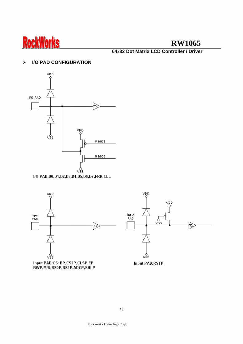
RW1065 64x32 Dot Matrix LCD Controller Driver
RockWorks Technology Corp
35
THE MPU INTERFACE (REFERENCE EXAMPLES) The RW1065 Series can be connected to 6800 Series MPUs The display area can be enlarged by using multiple RW1065 Series chips When this is done the chip select signal can be used to select the individual ICs to access
6800 Series MPUs
RW
106
5
RW1065 64x32 Dot Matrix LCD Controller Driver
RockWorks Technology Corp
36
When using external multi-level power supply for LCD driving (REFERENCE EXAMPLE)
Using a resistor divider can provide RW1065 external multi-level power supply for LCD driving
The circuit below shows a resistor divider network which can bias V0 V1 V2 V3 and V4 externally
RW1065 64x32 Dot Matrix LCD Controller Driver
RockWorks Technology Corp
37
bullWhen V0 V1 V2 V3 and V4 are biased by external power supply analog section of RW1065 should be turn off by software during LCD initialization The example in below shows the sequence to turn off analog section when external bias is used Begin of LCD initialization 1 Reset RW1065 2 SET EXT=1 (mode instruction)
RS RW DB7 DB6 DB5 DB4 DB3 DB2 DB1 DB00 0 0 0 0 0 1 1 0 1
3 SET Display Command (double command)
RS RW DB7 DB6 DB5 DB4 DB3 DB2 DB1 DB00 0 0 0 0 0 0 1 0 1 0 0 0 0 1 1 0 0 0 1
4 SET EXT=1 (mode instruction)
RS RW DB7 DB6 DB5 DB4 DB3 DB2 DB1 DB00 0 0 0 0 0 1 1 0 0
End of LCD initialization
bullBecause pins can not set LCD bias when external power supplies are used for LCD driving the bias can be set by an appropriate configuration for a resistor voltage divider networks The example is shown below
VSS
R
R
NR
R
R
RV1
RV2
RV3
RV4
V0
Bias Network Circuit Concept 15 Bias N=1 total = 5R 16 Bias N=2 total =6R 18 Bias N=4 total =8R 19 Bias N=5 total = 9R
RW1065 64x32 Dot Matrix LCD Controller Driver
RockWorks Technology Corp
38
Single chip solution for RW1065 application (REFERENCE EXAMPLE)
For a 64x32 application the duty cycle of LCD panel is 164 and the display duty of RW1065 should be set to 164 The display duty cycle can be selected by the DUTY bit in display command The diagram for 64x32 application is shown below
64 SEGx32COM LCD Panel
164 duty cycle
RW1065 DUTY=1
COM1~33
SEG1~65
RW1065 64x32 Dot Matrix LCD Controller Driver
RockWorks Technology Corp
39
Using an adjustable resistor on the main board to adjust the contrast of liquid crystal display (REFERENCE EXAMPLE)
The schematic shows an adjustable resistor on main board that can adjust voltage level of V0
RW1065 64x32 Dot Matrix LCD Controller Driver
RockWorks Technology Corp
40
Package information (Please pay close attention to the information in this section Do not hesitate to consult with our sale representative if you have any question or concern)
In order to make better bonding yield for RW1065 please follow the tips and recommendations in this section In this section few tips about COB footprint style PCB layout and wire bonding will be discussed
The drawing in below shows the PCB footprint style which we recommend for RW1065 Pads array in
curve shape is easier for Al wire bonding Besides that a real size COB footprint for RW1065 is also shown in below RW1065 COB footprint is also available in powerpcb or protel format for design reference purpose
The ratio is 11
RW1065 64x32 Dot Matrix LCD Controller Driver
RockWorks Technology Corp
41
During COB footprint design there have some tips about footprint that the PCB designer should know The angle between bonding wire and vertical line should less than 45 Otherwise the wire shorts would become very easy to happen at fours corners of the chip
The angle between bonding wire and vertical line could be reduced by expanding the distance between pads array and the chip In addition reducing length in horizon direction of pads array could minimize the angle between bonding wire and vertical line The picture in below will help to illustrate this concept From the experiences COB footprint style affects the bonding yield
Bad Wires are too close to each other
The angle between bonding wire and vertical line is greater than 45
The angle between bonding wire and vertical line is less than 45
Wires are not too close to each other
Reducing length in horizon direction of pads array could minimize the angle between bonding wire and vertical line
The angle between bonding wire and vertical line could be reduced by expanding the distance between pads array and the chip
RW1065 64x32 Dot Matrix LCD Controller Driver
RockWorks Technology Corp
42
If the gap between pads of COB footprint is filled with solder mask coating it is difficult to bond Al wire to
the pads The top solder masks layer that overlap COB footprint area should be removed
Please use 1 mils diameter Al wire for RW1065 wire bonding
1 2 3 4 5 6
A
B
C
D
654321
D
C
B
A
Title
Number RevisionSize
C
Date 29-Aug-2007 Sheet of File D公司資料99seMyDesignddb Drawn By
RW1065
COM131
COM142
COM153
COM164
COM175
COM186
COM197
COM208
COM219
COM2210
COM2311
COM2412
COM2513
COM2614
COM2715
COM2816
COM2917
COM3018
COM3119
SEG
6320
SEG
6221
SEG
6122
SEG
6023
SEG
5924
SEG
5825
SEG
5726
SEG
5627
SEG
5528
SEG
5429
SEG
5330
SEG
5231
SEG
5132
SEG
5033
SEG
4934
SEG
4835
SEG
4736
SEG
4637
SEG
4538
SEG
4439
SEG
4340
SEG
4241
SEG
4142
SEG
4043
SEG
3944
SEG
3845
SEG
3746
SEG
3647
SEG
3548
SEG
3449
SEG
3350
SEG
3251
SEG
3152
SEG
3053
SEG
2954
SEG
2855
SEG
2756
SEG
2657
SEG
2558
SEG
2459
SEG
2360
SEG
2261
SEG
2162
SEG
2063
SEG
1964
SEG
1865
SEG
1766
SEG
1667
SEG
1568
SEG
1469
SEG13 70SEG12 71SEG11 72SEG10 73SEG9 74SEG8 75SEG7 76SEG6 77SEG5 78SEG4 79SEG3 80SEG2 81SEG1 82SEG0 83ADCP 84CLL 85
VSS
86D
087
D1
88D
289
D3
90D
491
D5
92D
693
D7
94C
S1B
P95
CS2
P96
ERD
P97
AO
P(R
S)98
RW
RP
99V
DD
100
RST
P10
1C
LSP
102
FRR
103
MSP
104
BS1
P10
5B
S0P
106
SHLP
107
VD
D2
108
CA
P2N
109
CA
P2P
110
CA
P1P
111
CA
P1N
112
CA
P3P
113
VO
UT
114
V0
115
VR
AB
116
V3
117
V2
118
V4
119
V1
120
CO
M0
121
CO
M1
122
CO
M2
123
CO
M3
124
CO
M4
125
CO
M5
126
CO
M6
127
CO
M7
128
CO
M8
129
CO
M9
130
CO
M10
131
CO
M11
132
CO
M12
133
4897x1902 um
IC1
RW1065
C9CAPR4
100R0603
R30R0603
C8
CAP
C7
CAP
R2
100R0603
R1
0R0603C6 22uf
R50R
R6300R
R7RES1
R8NC R9
100R0603
VDD
R10
NC
R11
100R0603
R12
100R0603
R13
NC
R14
100R0603
R15
NC
VDD
D0
D1
D2
D3
D4
D5
D6
D7
DB[07]
VDDC5
01uf0603
VD
D
CS2
P
123456789
1011121314151617181920
J1
CON20
C1201uf0603
R3951K0603
VDD
CAP Value1UF~22UF
2XPut C6C8 Short R1R3Open R2R4C7C93XPut C6C8C9 R4Short R1Open R2R3C74XOpen R1R3
BS0 BS1 Bias0 0
0 1
1 0
11
15 bias
16 bias
18 bias
19 bias
ADC=0 SEG0lt~column address 00Hnormal(default) ADC=1 SEG0lt~column address 3FHinverted
SHL=0 Normal COM0~gtCOM63(default)SHL=1 Reverse direction COM63~gtCOM0
R16100R0603
LCD PANEL 64X32RockWorks
RW1065 64X32
COM0-31 SEG0-63SHL=0 ADC=0
SHL=1COM31-0
ADC=1SEG63-0
if use single chip for 32 command displaythe display command must select 164 dutyDisplay panel must select 164 duty type
VO
UT
C3P
C1N
C1P
C2P
C2N
VDD2
ADC
SHL
BS0
BS1
CLLADC
V1
V2
V3
V4
VR
AB
V0
VO
UT
C3P
C1N
C1P
C2P
C2N
VD
D2
SHL
BS0
BS1
FRR
RST
P
RW
RS
E CS1
B
CS1
V0RSRWED0D1D2D3D4D5D6D7
RSTPAK
C4
22uf
RBRES1
RA1RES1
C2
22uf
C1
22uf
C3
22uf
C0
22uf
R20
100k0603
R21
100k0603
R17
200K0603
V1
V2
V3
V4 VRAB
V0
V0
OPTION
B
R18
300R0603
RA2RES1
VADJ
R19100R
R23 RES1R22 0R
R24
RES1
R25
0R
VDD
CS1BP
CS2P
CS1
CS1
R26
22R0603
R27
22R0603
C1047uf
C11
01uf
VSS_INVDD_IN
D1DIODE
FGND
鐵框地
VSS
VDD
R28 10RR29 10RR30 10RR31 10RR32 10RR33 10RR34 10RR35 10RR36 10RR37 10RR38 10R
VADJ
1 2 3 4 5 6
A
B
C
D
654321
D
C
B
A
Title
Number RevisionSize
C
Date 29-Aug-2007 Sheet of File D公司資料99seMyDesignddb Drawn By
RW1065
COM131
COM142
COM153
COM164
COM175
COM186
COM197
COM208
COM219
COM2210
COM2311
COM2412
COM2513
COM2614
COM2715
COM2816
COM2917
COM3018
COM3119
SEG
6320
SEG
6221
SEG
6122
SEG
6023
SEG
5924
SEG
5825
SEG
5726
SEG
5627
SEG
5528
SEG
5429
SEG
5330
SEG
5231
SEG
5132
SEG
5033
SEG
4934
SEG
4835
SEG
4736
SEG
4637
SEG
4538
SEG
4439
SEG
4340
SEG
4241
SEG
4142
SEG
4043
SEG
3944
SEG
3845
SEG
3746
SEG
3647
SEG
3548
SEG
3449
SEG
3350
SEG
3251
SEG
3152
SEG
3053
SEG
2954
SEG
2855
SEG
2756
SEG
2657
SEG
2558
SEG
2459
SEG
2360
SEG
2261
SEG
2162
SEG
2063
SEG
1964
SEG
1865
SEG
1766
SEG
1667
SEG
1568
SEG
1469
SEG13 70SEG12 71SEG11 72SEG10 73SEG9 74SEG8 75SEG7 76SEG6 77SEG5 78SEG4 79SEG3 80SEG2 81SEG1 82SEG0 83ADCP 84CLL 85
VSS
86D
087
D1
88D
289
D3
90D
491
D5
92D
693
D7
94C
S1B
P95
CS2
P96
ERD
P97
AO
P(R
S)98
RW
RP
99V
DD
100
RST
P10
1C
LSP
102
FRR
103
MSP
104
BS1
P10
5B
S0P
106
SHLP
107
VD
D2
108
CA
P2N
109
CA
P2P
110
CA
P1P
111
CA
P1N
112
CA
P3P
113
VO
UT
114
V0
115
VR
AB
116
V3
117
V2
118
V4
119
V1
120
CO
M0
121
CO
M1
122
CO
M2
123
CO
M3
124
CO
M4
125
CO
M5
126
CO
M6
127
CO
M7
128
CO
M8
129
CO
M9
130
CO
M10
131
CO
M11
132
CO
M12
133
4897x1902 um
IC1
RW1065 Master
RW1065
COM131
COM142
COM153
COM164
COM175
COM186
COM197
COM208
COM219
COM2210
COM2311
COM2412
COM2513
COM2614
COM2715
COM2816
COM2917
COM3018
COM3119
SEG
6320
SEG
6221
SEG
6122
SEG
6023
SEG
5924
SEG
5825
SEG
5726
SEG
5627
SEG
5528
SEG
5429
SEG
5330
SEG
5231
SEG
5132
SEG
5033
SEG
4934
SEG
4835
SEG
4736
SEG
4637
SEG
4538
SEG
4439
SEG
4340
SEG
4241
SEG
4142
SEG
4043
SEG
3944
SEG
3845
SEG
3746
SEG
3647
SEG
3548
SEG
3449
SEG
3350
SEG
3251
SEG
3152
SEG
3053
SEG
2954
SEG
2855
SEG
2756
SEG
2657
SEG
2558
SEG
2459
SEG
2360
SEG
2261
SEG
2162
SEG
2063
SEG
1964
SEG
1865
SEG
1766
SEG
1667
SEG
1568
SEG
1469
SEG13 70SEG12 71SEG11 72SEG10 73SEG9 74SEG8 75SEG7 76SEG6 77SEG5 78SEG4 79SEG3 80SEG2 81SEG1 82SEG0 83ADCP 84CLL 85
VSS
86D
087
D1
88D
289
D3
90D
491
D5
92D
693
D7
94C
S1B
P95
CS2
P96
ERD
P97
AO
P(R
S)98
RW
RP
99V
DD
100
RST
P10
1C
LSP
102
FRR
103
MSP
104
BS1
P10
5B
S0P
106
SHLP
107
VD
D2
108
CA
P2N
109
CA
P2P
110
CA
P1P
111
CA
P1N
112
CA
P3P
113
VO
UT
114
V0
115
VR
AB
116
V3
117
V2
118
V4
119
V1
120
CO
M0
121
CO
M1
122
CO
M2
123
CO
M3
124
CO
M4
125
CO
M5
126
CO
M6
127
CO
M7
128
CO
M8
129
CO
M9
130
CO
M10
131
CO
M11
132
CO
M12
133
4897x1902 um
IC2
RW1065 Slave
C4
22uf
RBRES1
RA1RES1
C2
22uf
C1
22uf
C3
22uf
C0
22ufC9CAPR4
100R0603
R30R0603
C8
CAP
C7
CAP
R2
100R0603
R1
0R0603C6 22uf
R50R0603
R6300R0603
R7RES1
R8NC R9
100R0603
VDD
R10
NC
R11
100R0603
R12
NC
R13
100R0603
R14
100R0603
R15
NC
R16
100R0603
R17
NC
VDD
D0
D1
D2
D3
D4
D5
D6
D7
D0
D1
D2
D3
D4
D5
D6
D7
DB[07] DB[07]
VDDC10
01uf0603
VD
D
IC1_
CS2
P
VDD
IC2_
CS2
P
VD
D
C11
01uf0603
VSS
VSS
LCD PANEL 128X64
Master COM0-31 Slave COM32-63
Master SEG0-63 Slave SEG64-127
123456789
1011121314151617181920
J1
CON20
Master Slave
CAP Value1UF~22UF
2XPut C6C8 Short R1R3Open R2R4C7C93XPut C6C8C9 R4Short R1Open R2R3C74XOpen R1R3
RockWorksRW1065 128x64
BS0 BS1 Bias0 0
0 1
1 0
11
15 bias
16 bias
18 bias
19 bias
ADC=0 SEG0lt~column address 00Hnormal(default) ADC=1 SEG0lt~column address 3FHinverted
SHL=0 Normal COM0~gtCOM63(default)SHL=1 Reverse direction COM63~gtCOM0Both Master and Slave should set identical SHL value
SHL=0 SHL=0
ADC=0 ADC=0
Slave COM31-0
Slave SEG127-64
SHL=1
ADC=1
SHL=1Master COM63-32
ADC=1Master SEG63-0
R18100R0603
R22
100k0603
R23
100k0603
C501uF0603
R4551K0603
VDD
R19
200K0603
ADC1
ADC2
SHL
BS0
BS1
VDD2
V1
V2
V3
V4 VRAB
V0
V0V
OU
T
C3P
C1N
C1P
C2P
C2N
V1
V2
V3
V4
VR
AB
V0
VO
UT
C3P
C1N
C1P
C2P
C2N
VD
D2
SHL
BS0
BS1
FRR
RST
P
RW
RS
E IC1_
CS1
BP
V1
V2
V3
V4
VR
AB
V0
VO
UT
VD
D2
SHL
BS0
BS1
FRR
RST
P
RW
RS
E IC2_
CS1
BP
CLLADC1
CLLADC2
RSTP
CS1CS2
V0RSRWED0D1D2D3D4D5D6D7
AK
OPTION
R20
300R0603
RA2RES1
VADJ
R21
100R
B
R25 RESR24 0R
R26 RES R27 0RVDD
IC1_CS1BP
IC1_CS2P
CS1
CS1
R28 0R R29 RES
R30 RES R31 0R
IC2_CS1BP
IC2_CS2P
CS2
CS2
R32
22R0603
R33
22R0603
C1001uf
C11
47uf
D1DIODE
FGND
鐵框地
VSS
VDD
R34 10RR35 10RR36 10RR37 10RR38 10RR39 10RR40 10RR41 10RR42 10RR43 10RR44 10R
VSS_INVDD_IN
VADJ
VDD
1 2 3 4 5 6 7 8
A
B
C
D
87654321
D
C
B
A
Title
Number RevisionSize
D
Date 29-Aug-2007 Sheet of File D公司資料 99seMyDesignddb Drawn By
C422uf
RBRES1
RA1RES1
C3
22uf
C2
22uf
C1
22uf
C0
22ufC9CAPR4
100R0603
R30R0603
C8
CAP
C7
CAP
R2
100R0603
R1
0R0603C6 22uf
R220R0603
R23300R0603
R24RES1
R39
NCR40
100 ohm0603
VDD
R41
NC
R42
100 ohm0603
R43
NC
R44
100 ohm0603
R45
NC
R46
100 ohm0603
R47
100 ohm0603
R48
NC
R49
100 ohm0603
R50
NC
VDDCAP Value1UF~22UF
2XPut C6C8 Short R1R3Open R2R4C7C93XPut C6C8C9 R4Short R1Open R2R3C74XOpen R1R3
BS0 BS1 Bias0 0
0 1
1 0
11
15 bias
16 bias
18 bias
19 bias
ADC=0 SEG0lt~column address 00Hnormal(default)
ADC=1 SEG0lt~column address 3FHinverted
SHL=0 Normal COM0~gtCOM63(default)SHL=1 Reverse direction COM63~gtCOM0Both Master and Slave should set identical SHL value
R7
100k0603
R8
100k0603
V1
V2
V3
V4
V0
VRAB
V0
R5
200K
VDD2
VO
UT
C3P
C1N
C1P
C2P
C2N
ADC1
ADC2
ADC3
SHL
BS0
BS1
CS1CS2CS3
V0RSRWED0D1D2D3D4D5D6D7
RSTP
R3851K0603
C5
01uF
VDD
OPTION
R6
300R0603R9100R
RA2RES1
VADJ
RW1065
COM131
COM142
COM153
COM164
COM175
COM186
COM197
COM208
COM219
COM2210
COM2311
COM2412
COM2513
COM2614
COM2715
COM2816
COM2917
COM3018
COM3119
SEG
6320
SEG
6221
SEG
6122
SEG
6023
SEG
5924
SEG
5825
SEG
5726
SEG
5627
SEG
5528
SEG
5429
SEG
5330
SEG
5231
SEG
5132
SEG
5033
SEG
4934
SEG
4835
SEG
4736
SEG
4637
SEG
4538
SEG
4439
SEG
4340
SEG
4241
SEG
4142
SEG
4043
SEG
3944
SEG
3845
SEG
3746
SEG
3647
SEG
3548
SEG
3449
SEG
3350
SEG
3251
SEG
3152
SEG
3053
SEG
2954
SEG
2855
SEG
2756
SEG
2657
SEG
2558
SEG
2459
SEG
2360
SEG
2261
SEG
2162
SEG
2063
SEG
1964
SEG
1865
SEG
1766
SEG
1667
SEG
1568
SEG
1469
SEG13 70SEG12 71SEG11 72SEG10 73SEG9 74SEG8 75SEG7 76SEG6 77SEG5 78SEG4 79SEG3 80SEG2 81SEG1 82SEG0 83ADCP 84CLL 85
VSS
86D
087
D1
88D
289
D3
90D
491
D5
92D
693
D7
94C
S1B
P95
CS2
P96
ERD
P97
AO
P(R
S)98
RW
RP
99V
DD
100
RST
P10
1C
LSP
102
FRR
103
MSP
104
BS1
P10
5B
S0P
106
SHLP
107
VD
D2
108
CA
P2N
109
CA
P2P
110
CA
P1P
111
CA
P1N
112
CA
P3P
113
VO
UT
114
V0
115
VR
AB
116
V3
117
V2
118
V4
119
V1
120
CO
M0
121
CO
M1
122
CO
M2
123
CO
M3
124
CO
M4
125
CO
M5
126
CO
M6
127
CO
M7
128
CO
M8
129
CO
M9
130
CO
M10
131
CO
M11
132
CO
M12
133
4897x1902 um
IC1
RW1065 Master
RW1065
COM131
COM142
COM153
COM164
COM175
COM186
COM197
COM208
COM219
COM2210
COM2311
COM2412
COM2513
COM2614
COM2715
COM2816
COM2917
COM3018
COM3119
SEG
6320
SEG
6221
SEG
6122
SEG
6023
SEG
5924
SEG
5825
SEG
5726
SEG
5627
SEG
5528
SEG
5429
SEG
5330
SEG
5231
SEG
5132
SEG
5033
SEG
4934
SEG
4835
SEG
4736
SEG
4637
SEG
4538
SEG
4439
SEG
4340
SEG
4241
SEG
4142
SEG
4043
SEG
3944
SEG
3845
SEG
3746
SEG
3647
SEG
3548
SEG
3449
SEG
3350
SEG
3251
SEG
3152
SEG
3053
SEG
2954
SEG
2855
SEG
2756
SEG
2657
SEG
2558
SEG
2459
SEG
2360
SEG
2261
SEG
2162
SEG
2063
SEG
1964
SEG
1865
SEG
1766
SEG
1667
SEG
1568
SEG
1469
SEG13 70SEG12 71SEG11 72SEG10 73SEG9 74SEG8 75SEG7 76SEG6 77SEG5 78SEG4 79SEG3 80SEG2 81SEG1 82SEG0 83ADCP 84CLL 85
VSS
86D
087
D1
88D
289
D3
90D
491
D5
92D
693
D7
94C
S1B
P95
CS2
P96
ERD
P97
AO
P(R
S)98
RW
RP
99V
DD
100
RST
P10
1C
LSP
102
FRR
103
MSP
104
BS1
P10
5B
S0P
106
SHLP
107
VD
D2
108
CA
P2N
109
CA
P2P
110
CA
P1P
111
CA
P1N
112
CA
P3P
113
VO
UT
114
V0
115
VR
AB
116
V3
117
V2
118
V4
119
V1
120
CO
M0
121
CO
M1
122
CO
M2
123
CO
M3
124
CO
M4
125
CO
M5
126
CO
M6
127
CO
M7
128
CO
M8
129
CO
M9
130
CO
M10
131
CO
M11
132
CO
M12
133
4897x1902 um
IC2
RW1065 Slave
D0
D1
D2
D3
D4
D5
D6
D7
D0
D1
D2
D3
D4
D5
D6
D7
DB[07] DB[07]
VDDC8
01uf0603
VD
D
VDD
VD
D
C9
01uf0603
VSS
VSS
LCD PANEL 192X64
Master COM0-31 Slave COM32-63
Master SEG0-63 Slave SEG64-127
Master Slave
RockWorksRW1065 192x64
RW1065
COM131
COM142
COM153
COM164
COM175
COM186
COM197
COM208
COM219
COM2210
COM2311
COM2412
COM2513
COM2614
COM2715
COM2816
COM2917
COM3018
COM3119
SEG
6320
SEG
6221
SEG
6122
SEG
6023
SEG
5924
SEG
5825
SEG
5726
SEG
5627
SEG
5528
SEG
5429
SEG
5330
SEG
5231
SEG
5132
SEG
5033
SEG
4934
SEG
4835
SEG
4736
SEG
4637
SEG
4538
SEG
4439
SEG
4340
SEG
4241
SEG
4142
SEG
4043
SEG
3944
SEG
3845
SEG
3746
SEG
3647
SEG
3548
SEG
3449
SEG
3350
SEG
3251
SEG
3152
SEG
3053
SEG
2954
SEG
2855
SEG
2756
SEG
2657
SEG
2558
SEG
2459
SEG
2360
SEG
2261
SEG
2162
SEG
2063
SEG
1964
SEG
1865
SEG
1766
SEG
1667
SEG
1568
SEG
1469
SEG13 70SEG12 71SEG11 72SEG10 73SEG9 74SEG8 75SEG7 76SEG6 77SEG5 78SEG4 79SEG3 80SEG2 81SEG1 82SEG0 83ADCP 84CLL 85
VSS
86D
087
D1
88D
289
D3
90D
491
D5
92D
693
D7
94C
S1B
P95
CS2
P96
ERD
P97
AO
P(R
S)98
RW
RP
99V
DD
100
RST
P10
1C
LSP
102
FRR
103
MSP
104
BS1
P10
5B
S0P
106
SHLP
107
VD
D2
108
CA
P2N
109
CA
P2P
110
CA
P1P
111
CA
P1N
112
CA
P3P
113
VO
UT
114
V0
115
VR
AB
116
V3
117
V2
118
V4
119
V1
120
CO
M0
121
CO
M1
122
CO
M2
123
CO
M3
124
CO
M4
125
CO
M5
126
CO
M6
127
CO
M7
128
CO
M8
129
CO
M9
130
CO
M10
131
CO
M11
132
CO
M12
133
4897x1902 um
IC3
RW1065 Slave
D0
D1
D2
D3
D4
D5
D6
D7
DB[07]
VSS
VSS
VDD
VD
D
C10
01uf0603
Slave SEG128-192
Slave
SHL=0 SHL=0
Master COM63-32SHL=1 SHL=1
Slave COM31-0ADC=0 ADC=0 ADC=0
ADC=1 ADC=1 ADC=1Master SEG63-0 Slave SEG127-64 Slave SEG192-128
R50100R0603
V1
V2
V3
V4
VR
AB
V0
VO
UT
C3P
C1N
C1P
C2P
C2N
VD
D2
SHL
BS0
BS1
FRR
RST
P
RW
RS
E V1
V2
V3
V4
VR
AB
V0
VO
UT
VD
D2
SHL
BS0
BS1
FRR
RST
P
RW
RS
E V1
V2
V3
V4
VR
AB
V0
VO
UT
VD
D2
SHL
BS0
BS1
FRR
RST
P
RW
RS
E
CLL CLL CLLADC1 ADC2 ADC3
R25 10RR26 10RR27 10RR28 10RR29 10RR30 10RR31 10RR32 10RR33 10RR34 10RR35 10R
R36
22R0603
D1DIODE
R3722R0603
C647uf
C701uf
VSS_INVDD_IN
VSS
VDD
VADJ
123456789
101112131415161718192021222324
J1
CON24
AK
FGND
鐵框地
IC1_
CS1
BP
IC1_
CS2
P
IC2_
CS2
PIC
2_C
S1B
P
IC3_
CS1
BP
IC3_
CS2
B
R10 0R R11 RES
R12 RES R13 0RVDD
IC1_CS2B
IC1_CS1BPCS1
CS1
R14 0R R15 RES
R16 RES R17 0RVDDIC2_CS2B
IC2_CS1BPCS2
CS2
R18 0R R19 RES
R20 RES R21 0RVDDIC3_CS2B
IC3_CS1BPCS3
CS3
B
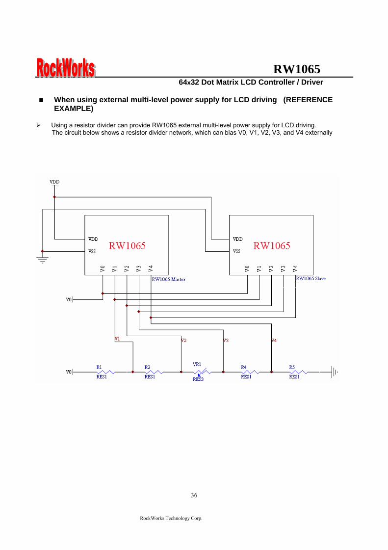
RW1065 64x32 Dot Matrix LCD Controller Driver
RockWorks Technology Corp
36
When using external multi-level power supply for LCD driving (REFERENCE EXAMPLE)
Using a resistor divider can provide RW1065 external multi-level power supply for LCD driving
The circuit below shows a resistor divider network which can bias V0 V1 V2 V3 and V4 externally
RW1065 64x32 Dot Matrix LCD Controller Driver
RockWorks Technology Corp
37
bullWhen V0 V1 V2 V3 and V4 are biased by external power supply analog section of RW1065 should be turn off by software during LCD initialization The example in below shows the sequence to turn off analog section when external bias is used Begin of LCD initialization 1 Reset RW1065 2 SET EXT=1 (mode instruction)
RS RW DB7 DB6 DB5 DB4 DB3 DB2 DB1 DB00 0 0 0 0 0 1 1 0 1
3 SET Display Command (double command)
RS RW DB7 DB6 DB5 DB4 DB3 DB2 DB1 DB00 0 0 0 0 0 0 1 0 1 0 0 0 0 1 1 0 0 0 1
4 SET EXT=1 (mode instruction)
RS RW DB7 DB6 DB5 DB4 DB3 DB2 DB1 DB00 0 0 0 0 0 1 1 0 0
End of LCD initialization
bullBecause pins can not set LCD bias when external power supplies are used for LCD driving the bias can be set by an appropriate configuration for a resistor voltage divider networks The example is shown below
VSS
R
R
NR
R
R
RV1
RV2
RV3
RV4
V0
Bias Network Circuit Concept 15 Bias N=1 total = 5R 16 Bias N=2 total =6R 18 Bias N=4 total =8R 19 Bias N=5 total = 9R
RW1065 64x32 Dot Matrix LCD Controller Driver
RockWorks Technology Corp
38
Single chip solution for RW1065 application (REFERENCE EXAMPLE)
For a 64x32 application the duty cycle of LCD panel is 164 and the display duty of RW1065 should be set to 164 The display duty cycle can be selected by the DUTY bit in display command The diagram for 64x32 application is shown below
64 SEGx32COM LCD Panel
164 duty cycle
RW1065 DUTY=1
COM1~33
SEG1~65
RW1065 64x32 Dot Matrix LCD Controller Driver
RockWorks Technology Corp
39
Using an adjustable resistor on the main board to adjust the contrast of liquid crystal display (REFERENCE EXAMPLE)
The schematic shows an adjustable resistor on main board that can adjust voltage level of V0
RW1065 64x32 Dot Matrix LCD Controller Driver
RockWorks Technology Corp
40
Package information (Please pay close attention to the information in this section Do not hesitate to consult with our sale representative if you have any question or concern)
In order to make better bonding yield for RW1065 please follow the tips and recommendations in this section In this section few tips about COB footprint style PCB layout and wire bonding will be discussed
The drawing in below shows the PCB footprint style which we recommend for RW1065 Pads array in
curve shape is easier for Al wire bonding Besides that a real size COB footprint for RW1065 is also shown in below RW1065 COB footprint is also available in powerpcb or protel format for design reference purpose
The ratio is 11
RW1065 64x32 Dot Matrix LCD Controller Driver
RockWorks Technology Corp
41
During COB footprint design there have some tips about footprint that the PCB designer should know The angle between bonding wire and vertical line should less than 45 Otherwise the wire shorts would become very easy to happen at fours corners of the chip
The angle between bonding wire and vertical line could be reduced by expanding the distance between pads array and the chip In addition reducing length in horizon direction of pads array could minimize the angle between bonding wire and vertical line The picture in below will help to illustrate this concept From the experiences COB footprint style affects the bonding yield
Bad Wires are too close to each other
The angle between bonding wire and vertical line is greater than 45
The angle between bonding wire and vertical line is less than 45
Wires are not too close to each other
Reducing length in horizon direction of pads array could minimize the angle between bonding wire and vertical line
The angle between bonding wire and vertical line could be reduced by expanding the distance between pads array and the chip
RW1065 64x32 Dot Matrix LCD Controller Driver
RockWorks Technology Corp
42
If the gap between pads of COB footprint is filled with solder mask coating it is difficult to bond Al wire to
the pads The top solder masks layer that overlap COB footprint area should be removed
Please use 1 mils diameter Al wire for RW1065 wire bonding
1 2 3 4 5 6
A
B
C
D
654321
D
C
B
A
Title
Number RevisionSize
C
Date 29-Aug-2007 Sheet of File D公司資料99seMyDesignddb Drawn By
RW1065
COM131
COM142
COM153
COM164
COM175
COM186
COM197
COM208
COM219
COM2210
COM2311
COM2412
COM2513
COM2614
COM2715
COM2816
COM2917
COM3018
COM3119
SEG
6320
SEG
6221
SEG
6122
SEG
6023
SEG
5924
SEG
5825
SEG
5726
SEG
5627
SEG
5528
SEG
5429
SEG
5330
SEG
5231
SEG
5132
SEG
5033
SEG
4934
SEG
4835
SEG
4736
SEG
4637
SEG
4538
SEG
4439
SEG
4340
SEG
4241
SEG
4142
SEG
4043
SEG
3944
SEG
3845
SEG
3746
SEG
3647
SEG
3548
SEG
3449
SEG
3350
SEG
3251
SEG
3152
SEG
3053
SEG
2954
SEG
2855
SEG
2756
SEG
2657
SEG
2558
SEG
2459
SEG
2360
SEG
2261
SEG
2162
SEG
2063
SEG
1964
SEG
1865
SEG
1766
SEG
1667
SEG
1568
SEG
1469
SEG13 70SEG12 71SEG11 72SEG10 73SEG9 74SEG8 75SEG7 76SEG6 77SEG5 78SEG4 79SEG3 80SEG2 81SEG1 82SEG0 83ADCP 84CLL 85
VSS
86D
087
D1
88D
289
D3
90D
491
D5
92D
693
D7
94C
S1B
P95
CS2
P96
ERD
P97
AO
P(R
S)98
RW
RP
99V
DD
100
RST
P10
1C
LSP
102
FRR
103
MSP
104
BS1
P10
5B
S0P
106
SHLP
107
VD
D2
108
CA
P2N
109
CA
P2P
110
CA
P1P
111
CA
P1N
112
CA
P3P
113
VO
UT
114
V0
115
VR
AB
116
V3
117
V2
118
V4
119
V1
120
CO
M0
121
CO
M1
122
CO
M2
123
CO
M3
124
CO
M4
125
CO
M5
126
CO
M6
127
CO
M7
128
CO
M8
129
CO
M9
130
CO
M10
131
CO
M11
132
CO
M12
133
4897x1902 um
IC1
RW1065
C9CAPR4
100R0603
R30R0603
C8
CAP
C7
CAP
R2
100R0603
R1
0R0603C6 22uf
R50R
R6300R
R7RES1
R8NC R9
100R0603
VDD
R10
NC
R11
100R0603
R12
100R0603
R13
NC
R14
100R0603
R15
NC
VDD
D0
D1
D2
D3
D4
D5
D6
D7
DB[07]
VDDC5
01uf0603
VD
D
CS2
P
123456789
1011121314151617181920
J1
CON20
C1201uf0603
R3951K0603
VDD
CAP Value1UF~22UF
2XPut C6C8 Short R1R3Open R2R4C7C93XPut C6C8C9 R4Short R1Open R2R3C74XOpen R1R3
BS0 BS1 Bias0 0
0 1
1 0
11
15 bias
16 bias
18 bias
19 bias
ADC=0 SEG0lt~column address 00Hnormal(default) ADC=1 SEG0lt~column address 3FHinverted
SHL=0 Normal COM0~gtCOM63(default)SHL=1 Reverse direction COM63~gtCOM0
R16100R0603
LCD PANEL 64X32RockWorks
RW1065 64X32
COM0-31 SEG0-63SHL=0 ADC=0
SHL=1COM31-0
ADC=1SEG63-0
if use single chip for 32 command displaythe display command must select 164 dutyDisplay panel must select 164 duty type
VO
UT
C3P
C1N
C1P
C2P
C2N
VDD2
ADC
SHL
BS0
BS1
CLLADC
V1
V2
V3
V4
VR
AB
V0
VO
UT
C3P
C1N
C1P
C2P
C2N
VD
D2
SHL
BS0
BS1
FRR
RST
P
RW
RS
E CS1
B
CS1
V0RSRWED0D1D2D3D4D5D6D7
RSTPAK
C4
22uf
RBRES1
RA1RES1
C2
22uf
C1
22uf
C3
22uf
C0
22uf
R20
100k0603
R21
100k0603
R17
200K0603
V1
V2
V3
V4 VRAB
V0
V0
OPTION
B
R18
300R0603
RA2RES1
VADJ
R19100R
R23 RES1R22 0R
R24
RES1
R25
0R
VDD
CS1BP
CS2P
CS1
CS1
R26
22R0603
R27
22R0603
C1047uf
C11
01uf
VSS_INVDD_IN
D1DIODE
FGND
鐵框地
VSS
VDD
R28 10RR29 10RR30 10RR31 10RR32 10RR33 10RR34 10RR35 10RR36 10RR37 10RR38 10R
VADJ
1 2 3 4 5 6
A
B
C
D
654321
D
C
B
A
Title
Number RevisionSize
C
Date 29-Aug-2007 Sheet of File D公司資料99seMyDesignddb Drawn By
RW1065
COM131
COM142
COM153
COM164
COM175
COM186
COM197
COM208
COM219
COM2210
COM2311
COM2412
COM2513
COM2614
COM2715
COM2816
COM2917
COM3018
COM3119
SEG
6320
SEG
6221
SEG
6122
SEG
6023
SEG
5924
SEG
5825
SEG
5726
SEG
5627
SEG
5528
SEG
5429
SEG
5330
SEG
5231
SEG
5132
SEG
5033
SEG
4934
SEG
4835
SEG
4736
SEG
4637
SEG
4538
SEG
4439
SEG
4340
SEG
4241
SEG
4142
SEG
4043
SEG
3944
SEG
3845
SEG
3746
SEG
3647
SEG
3548
SEG
3449
SEG
3350
SEG
3251
SEG
3152
SEG
3053
SEG
2954
SEG
2855
SEG
2756
SEG
2657
SEG
2558
SEG
2459
SEG
2360
SEG
2261
SEG
2162
SEG
2063
SEG
1964
SEG
1865
SEG
1766
SEG
1667
SEG
1568
SEG
1469
SEG13 70SEG12 71SEG11 72SEG10 73SEG9 74SEG8 75SEG7 76SEG6 77SEG5 78SEG4 79SEG3 80SEG2 81SEG1 82SEG0 83ADCP 84CLL 85
VSS
86D
087
D1
88D
289
D3
90D
491
D5
92D
693
D7
94C
S1B
P95
CS2
P96
ERD
P97
AO
P(R
S)98
RW
RP
99V
DD
100
RST
P10
1C
LSP
102
FRR
103
MSP
104
BS1
P10
5B
S0P
106
SHLP
107
VD
D2
108
CA
P2N
109
CA
P2P
110
CA
P1P
111
CA
P1N
112
CA
P3P
113
VO
UT
114
V0
115
VR
AB
116
V3
117
V2
118
V4
119
V1
120
CO
M0
121
CO
M1
122
CO
M2
123
CO
M3
124
CO
M4
125
CO
M5
126
CO
M6
127
CO
M7
128
CO
M8
129
CO
M9
130
CO
M10
131
CO
M11
132
CO
M12
133
4897x1902 um
IC1
RW1065 Master
RW1065
COM131
COM142
COM153
COM164
COM175
COM186
COM197
COM208
COM219
COM2210
COM2311
COM2412
COM2513
COM2614
COM2715
COM2816
COM2917
COM3018
COM3119
SEG
6320
SEG
6221
SEG
6122
SEG
6023
SEG
5924
SEG
5825
SEG
5726
SEG
5627
SEG
5528
SEG
5429
SEG
5330
SEG
5231
SEG
5132
SEG
5033
SEG
4934
SEG
4835
SEG
4736
SEG
4637
SEG
4538
SEG
4439
SEG
4340
SEG
4241
SEG
4142
SEG
4043
SEG
3944
SEG
3845
SEG
3746
SEG
3647
SEG
3548
SEG
3449
SEG
3350
SEG
3251
SEG
3152
SEG
3053
SEG
2954
SEG
2855
SEG
2756
SEG
2657
SEG
2558
SEG
2459
SEG
2360
SEG
2261
SEG
2162
SEG
2063
SEG
1964
SEG
1865
SEG
1766
SEG
1667
SEG
1568
SEG
1469
SEG13 70SEG12 71SEG11 72SEG10 73SEG9 74SEG8 75SEG7 76SEG6 77SEG5 78SEG4 79SEG3 80SEG2 81SEG1 82SEG0 83ADCP 84CLL 85
VSS
86D
087
D1
88D
289
D3
90D
491
D5
92D
693
D7
94C
S1B
P95
CS2
P96
ERD
P97
AO
P(R
S)98
RW
RP
99V
DD
100
RST
P10
1C
LSP
102
FRR
103
MSP
104
BS1
P10
5B
S0P
106
SHLP
107
VD
D2
108
CA
P2N
109
CA
P2P
110
CA
P1P
111
CA
P1N
112
CA
P3P
113
VO
UT
114
V0
115
VR
AB
116
V3
117
V2
118
V4
119
V1
120
CO
M0
121
CO
M1
122
CO
M2
123
CO
M3
124
CO
M4
125
CO
M5
126
CO
M6
127
CO
M7
128
CO
M8
129
CO
M9
130
CO
M10
131
CO
M11
132
CO
M12
133
4897x1902 um
IC2
RW1065 Slave
C4
22uf
RBRES1
RA1RES1
C2
22uf
C1
22uf
C3
22uf
C0
22ufC9CAPR4
100R0603
R30R0603
C8
CAP
C7
CAP
R2
100R0603
R1
0R0603C6 22uf
R50R0603
R6300R0603
R7RES1
R8NC R9
100R0603
VDD
R10
NC
R11
100R0603
R12
NC
R13
100R0603
R14
100R0603
R15
NC
R16
100R0603
R17
NC
VDD
D0
D1
D2
D3
D4
D5
D6
D7
D0
D1
D2
D3
D4
D5
D6
D7
DB[07] DB[07]
VDDC10
01uf0603
VD
D
IC1_
CS2
P
VDD
IC2_
CS2
P
VD
D
C11
01uf0603
VSS
VSS
LCD PANEL 128X64
Master COM0-31 Slave COM32-63
Master SEG0-63 Slave SEG64-127
123456789
1011121314151617181920
J1
CON20
Master Slave
CAP Value1UF~22UF
2XPut C6C8 Short R1R3Open R2R4C7C93XPut C6C8C9 R4Short R1Open R2R3C74XOpen R1R3
RockWorksRW1065 128x64
BS0 BS1 Bias0 0
0 1
1 0
11
15 bias
16 bias
18 bias
19 bias
ADC=0 SEG0lt~column address 00Hnormal(default) ADC=1 SEG0lt~column address 3FHinverted
SHL=0 Normal COM0~gtCOM63(default)SHL=1 Reverse direction COM63~gtCOM0Both Master and Slave should set identical SHL value
SHL=0 SHL=0
ADC=0 ADC=0
Slave COM31-0
Slave SEG127-64
SHL=1
ADC=1
SHL=1Master COM63-32
ADC=1Master SEG63-0
R18100R0603
R22
100k0603
R23
100k0603
C501uF0603
R4551K0603
VDD
R19
200K0603
ADC1
ADC2
SHL
BS0
BS1
VDD2
V1
V2
V3
V4 VRAB
V0
V0V
OU
T
C3P
C1N
C1P
C2P
C2N
V1
V2
V3
V4
VR
AB
V0
VO
UT
C3P
C1N
C1P
C2P
C2N
VD
D2
SHL
BS0
BS1
FRR
RST
P
RW
RS
E IC1_
CS1
BP
V1
V2
V3
V4
VR
AB
V0
VO
UT
VD
D2
SHL
BS0
BS1
FRR
RST
P
RW
RS
E IC2_
CS1
BP
CLLADC1
CLLADC2
RSTP
CS1CS2
V0RSRWED0D1D2D3D4D5D6D7
AK
OPTION
R20
300R0603
RA2RES1
VADJ
R21
100R
B
R25 RESR24 0R
R26 RES R27 0RVDD
IC1_CS1BP
IC1_CS2P
CS1
CS1
R28 0R R29 RES
R30 RES R31 0R
IC2_CS1BP
IC2_CS2P
CS2
CS2
R32
22R0603
R33
22R0603
C1001uf
C11
47uf
D1DIODE
FGND
鐵框地
VSS
VDD
R34 10RR35 10RR36 10RR37 10RR38 10RR39 10RR40 10RR41 10RR42 10RR43 10RR44 10R
VSS_INVDD_IN
VADJ
VDD
1 2 3 4 5 6 7 8
A
B
C
D
87654321
D
C
B
A
Title
Number RevisionSize
D
Date 29-Aug-2007 Sheet of File D公司資料 99seMyDesignddb Drawn By
C422uf
RBRES1
RA1RES1
C3
22uf
C2
22uf
C1
22uf
C0
22ufC9CAPR4
100R0603
R30R0603
C8
CAP
C7
CAP
R2
100R0603
R1
0R0603C6 22uf
R220R0603
R23300R0603
R24RES1
R39
NCR40
100 ohm0603
VDD
R41
NC
R42
100 ohm0603
R43
NC
R44
100 ohm0603
R45
NC
R46
100 ohm0603
R47
100 ohm0603
R48
NC
R49
100 ohm0603
R50
NC
VDDCAP Value1UF~22UF
2XPut C6C8 Short R1R3Open R2R4C7C93XPut C6C8C9 R4Short R1Open R2R3C74XOpen R1R3
BS0 BS1 Bias0 0
0 1
1 0
11
15 bias
16 bias
18 bias
19 bias
ADC=0 SEG0lt~column address 00Hnormal(default)
ADC=1 SEG0lt~column address 3FHinverted
SHL=0 Normal COM0~gtCOM63(default)SHL=1 Reverse direction COM63~gtCOM0Both Master and Slave should set identical SHL value
R7
100k0603
R8
100k0603
V1
V2
V3
V4
V0
VRAB
V0
R5
200K
VDD2
VO
UT
C3P
C1N
C1P
C2P
C2N
ADC1
ADC2
ADC3
SHL
BS0
BS1
CS1CS2CS3
V0RSRWED0D1D2D3D4D5D6D7
RSTP
R3851K0603
C5
01uF
VDD
OPTION
R6
300R0603R9100R
RA2RES1
VADJ
RW1065
COM131
COM142
COM153
COM164
COM175
COM186
COM197
COM208
COM219
COM2210
COM2311
COM2412
COM2513
COM2614
COM2715
COM2816
COM2917
COM3018
COM3119
SEG
6320
SEG
6221
SEG
6122
SEG
6023
SEG
5924
SEG
5825
SEG
5726
SEG
5627
SEG
5528
SEG
5429
SEG
5330
SEG
5231
SEG
5132
SEG
5033
SEG
4934
SEG
4835
SEG
4736
SEG
4637
SEG
4538
SEG
4439
SEG
4340
SEG
4241
SEG
4142
SEG
4043
SEG
3944
SEG
3845
SEG
3746
SEG
3647
SEG
3548
SEG
3449
SEG
3350
SEG
3251
SEG
3152
SEG
3053
SEG
2954
SEG
2855
SEG
2756
SEG
2657
SEG
2558
SEG
2459
SEG
2360
SEG
2261
SEG
2162
SEG
2063
SEG
1964
SEG
1865
SEG
1766
SEG
1667
SEG
1568
SEG
1469
SEG13 70SEG12 71SEG11 72SEG10 73SEG9 74SEG8 75SEG7 76SEG6 77SEG5 78SEG4 79SEG3 80SEG2 81SEG1 82SEG0 83ADCP 84CLL 85
VSS
86D
087
D1
88D
289
D3
90D
491
D5
92D
693
D7
94C
S1B
P95
CS2
P96
ERD
P97
AO
P(R
S)98
RW
RP
99V
DD
100
RST
P10
1C
LSP
102
FRR
103
MSP
104
BS1
P10
5B
S0P
106
SHLP
107
VD
D2
108
CA
P2N
109
CA
P2P
110
CA
P1P
111
CA
P1N
112
CA
P3P
113
VO
UT
114
V0
115
VR
AB
116
V3
117
V2
118
V4
119
V1
120
CO
M0
121
CO
M1
122
CO
M2
123
CO
M3
124
CO
M4
125
CO
M5
126
CO
M6
127
CO
M7
128
CO
M8
129
CO
M9
130
CO
M10
131
CO
M11
132
CO
M12
133
4897x1902 um
IC1
RW1065 Master
RW1065
COM131
COM142
COM153
COM164
COM175
COM186
COM197
COM208
COM219
COM2210
COM2311
COM2412
COM2513
COM2614
COM2715
COM2816
COM2917
COM3018
COM3119
SEG
6320
SEG
6221
SEG
6122
SEG
6023
SEG
5924
SEG
5825
SEG
5726
SEG
5627
SEG
5528
SEG
5429
SEG
5330
SEG
5231
SEG
5132
SEG
5033
SEG
4934
SEG
4835
SEG
4736
SEG
4637
SEG
4538
SEG
4439
SEG
4340
SEG
4241
SEG
4142
SEG
4043
SEG
3944
SEG
3845
SEG
3746
SEG
3647
SEG
3548
SEG
3449
SEG
3350
SEG
3251
SEG
3152
SEG
3053
SEG
2954
SEG
2855
SEG
2756
SEG
2657
SEG
2558
SEG
2459
SEG
2360
SEG
2261
SEG
2162
SEG
2063
SEG
1964
SEG
1865
SEG
1766
SEG
1667
SEG
1568
SEG
1469
SEG13 70SEG12 71SEG11 72SEG10 73SEG9 74SEG8 75SEG7 76SEG6 77SEG5 78SEG4 79SEG3 80SEG2 81SEG1 82SEG0 83ADCP 84CLL 85
VSS
86D
087
D1
88D
289
D3
90D
491
D5
92D
693
D7
94C
S1B
P95
CS2
P96
ERD
P97
AO
P(R
S)98
RW
RP
99V
DD
100
RST
P10
1C
LSP
102
FRR
103
MSP
104
BS1
P10
5B
S0P
106
SHLP
107
VD
D2
108
CA
P2N
109
CA
P2P
110
CA
P1P
111
CA
P1N
112
CA
P3P
113
VO
UT
114
V0
115
VR
AB
116
V3
117
V2
118
V4
119
V1
120
CO
M0
121
CO
M1
122
CO
M2
123
CO
M3
124
CO
M4
125
CO
M5
126
CO
M6
127
CO
M7
128
CO
M8
129
CO
M9
130
CO
M10
131
CO
M11
132
CO
M12
133
4897x1902 um
IC2
RW1065 Slave
D0
D1
D2
D3
D4
D5
D6
D7
D0
D1
D2
D3
D4
D5
D6
D7
DB[07] DB[07]
VDDC8
01uf0603
VD
D
VDD
VD
D
C9
01uf0603
VSS
VSS
LCD PANEL 192X64
Master COM0-31 Slave COM32-63
Master SEG0-63 Slave SEG64-127
Master Slave
RockWorksRW1065 192x64
RW1065
COM131
COM142
COM153
COM164
COM175
COM186
COM197
COM208
COM219
COM2210
COM2311
COM2412
COM2513
COM2614
COM2715
COM2816
COM2917
COM3018
COM3119
SEG
6320
SEG
6221
SEG
6122
SEG
6023
SEG
5924
SEG
5825
SEG
5726
SEG
5627
SEG
5528
SEG
5429
SEG
5330
SEG
5231
SEG
5132
SEG
5033
SEG
4934
SEG
4835
SEG
4736
SEG
4637
SEG
4538
SEG
4439
SEG
4340
SEG
4241
SEG
4142
SEG
4043
SEG
3944
SEG
3845
SEG
3746
SEG
3647
SEG
3548
SEG
3449
SEG
3350
SEG
3251
SEG
3152
SEG
3053
SEG
2954
SEG
2855
SEG
2756
SEG
2657
SEG
2558
SEG
2459
SEG
2360
SEG
2261
SEG
2162
SEG
2063
SEG
1964
SEG
1865
SEG
1766
SEG
1667
SEG
1568
SEG
1469
SEG13 70SEG12 71SEG11 72SEG10 73SEG9 74SEG8 75SEG7 76SEG6 77SEG5 78SEG4 79SEG3 80SEG2 81SEG1 82SEG0 83ADCP 84CLL 85
VSS
86D
087
D1
88D
289
D3
90D
491
D5
92D
693
D7
94C
S1B
P95
CS2
P96
ERD
P97
AO
P(R
S)98
RW
RP
99V
DD
100
RST
P10
1C
LSP
102
FRR
103
MSP
104
BS1
P10
5B
S0P
106
SHLP
107
VD
D2
108
CA
P2N
109
CA
P2P
110
CA
P1P
111
CA
P1N
112
CA
P3P
113
VO
UT
114
V0
115
VR
AB
116
V3
117
V2
118
V4
119
V1
120
CO
M0
121
CO
M1
122
CO
M2
123
CO
M3
124
CO
M4
125
CO
M5
126
CO
M6
127
CO
M7
128
CO
M8
129
CO
M9
130
CO
M10
131
CO
M11
132
CO
M12
133
4897x1902 um
IC3
RW1065 Slave
D0
D1
D2
D3
D4
D5
D6
D7
DB[07]
VSS
VSS
VDD
VD
D
C10
01uf0603
Slave SEG128-192
Slave
SHL=0 SHL=0
Master COM63-32SHL=1 SHL=1
Slave COM31-0ADC=0 ADC=0 ADC=0
ADC=1 ADC=1 ADC=1Master SEG63-0 Slave SEG127-64 Slave SEG192-128
R50100R0603
V1
V2
V3
V4
VR
AB
V0
VO
UT
C3P
C1N
C1P
C2P
C2N
VD
D2
SHL
BS0
BS1
FRR
RST
P
RW
RS
E V1
V2
V3
V4
VR
AB
V0
VO
UT
VD
D2
SHL
BS0
BS1
FRR
RST
P
RW
RS
E V1
V2
V3
V4
VR
AB
V0
VO
UT
VD
D2
SHL
BS0
BS1
FRR
RST
P
RW
RS
E
CLL CLL CLLADC1 ADC2 ADC3
R25 10RR26 10RR27 10RR28 10RR29 10RR30 10RR31 10RR32 10RR33 10RR34 10RR35 10R
R36
22R0603
D1DIODE
R3722R0603
C647uf
C701uf
VSS_INVDD_IN
VSS
VDD
VADJ
123456789
101112131415161718192021222324
J1
CON24
AK
FGND
鐵框地
IC1_
CS1
BP
IC1_
CS2
P
IC2_
CS2
PIC
2_C
S1B
P
IC3_
CS1
BP
IC3_
CS2
B
R10 0R R11 RES
R12 RES R13 0RVDD
IC1_CS2B
IC1_CS1BPCS1
CS1
R14 0R R15 RES
R16 RES R17 0RVDDIC2_CS2B
IC2_CS1BPCS2
CS2
R18 0R R19 RES
R20 RES R21 0RVDDIC3_CS2B
IC3_CS1BPCS3
CS3
B
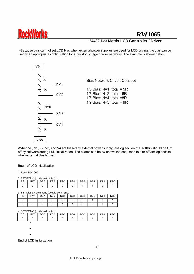
RW1065 64x32 Dot Matrix LCD Controller Driver
RockWorks Technology Corp
37
bullWhen V0 V1 V2 V3 and V4 are biased by external power supply analog section of RW1065 should be turn off by software during LCD initialization The example in below shows the sequence to turn off analog section when external bias is used Begin of LCD initialization 1 Reset RW1065 2 SET EXT=1 (mode instruction)
RS RW DB7 DB6 DB5 DB4 DB3 DB2 DB1 DB00 0 0 0 0 0 1 1 0 1
3 SET Display Command (double command)
RS RW DB7 DB6 DB5 DB4 DB3 DB2 DB1 DB00 0 0 0 0 0 0 1 0 1 0 0 0 0 1 1 0 0 0 1
4 SET EXT=1 (mode instruction)
RS RW DB7 DB6 DB5 DB4 DB3 DB2 DB1 DB00 0 0 0 0 0 1 1 0 0
End of LCD initialization
bullBecause pins can not set LCD bias when external power supplies are used for LCD driving the bias can be set by an appropriate configuration for a resistor voltage divider networks The example is shown below
VSS
R
R
NR
R
R
RV1
RV2
RV3
RV4
V0
Bias Network Circuit Concept 15 Bias N=1 total = 5R 16 Bias N=2 total =6R 18 Bias N=4 total =8R 19 Bias N=5 total = 9R
RW1065 64x32 Dot Matrix LCD Controller Driver
RockWorks Technology Corp
38
Single chip solution for RW1065 application (REFERENCE EXAMPLE)
For a 64x32 application the duty cycle of LCD panel is 164 and the display duty of RW1065 should be set to 164 The display duty cycle can be selected by the DUTY bit in display command The diagram for 64x32 application is shown below
64 SEGx32COM LCD Panel
164 duty cycle
RW1065 DUTY=1
COM1~33
SEG1~65
RW1065 64x32 Dot Matrix LCD Controller Driver
RockWorks Technology Corp
39
Using an adjustable resistor on the main board to adjust the contrast of liquid crystal display (REFERENCE EXAMPLE)
The schematic shows an adjustable resistor on main board that can adjust voltage level of V0
RW1065 64x32 Dot Matrix LCD Controller Driver
RockWorks Technology Corp
40
Package information (Please pay close attention to the information in this section Do not hesitate to consult with our sale representative if you have any question or concern)
In order to make better bonding yield for RW1065 please follow the tips and recommendations in this section In this section few tips about COB footprint style PCB layout and wire bonding will be discussed
The drawing in below shows the PCB footprint style which we recommend for RW1065 Pads array in
curve shape is easier for Al wire bonding Besides that a real size COB footprint for RW1065 is also shown in below RW1065 COB footprint is also available in powerpcb or protel format for design reference purpose
The ratio is 11
RW1065 64x32 Dot Matrix LCD Controller Driver
RockWorks Technology Corp
41
During COB footprint design there have some tips about footprint that the PCB designer should know The angle between bonding wire and vertical line should less than 45 Otherwise the wire shorts would become very easy to happen at fours corners of the chip
The angle between bonding wire and vertical line could be reduced by expanding the distance between pads array and the chip In addition reducing length in horizon direction of pads array could minimize the angle between bonding wire and vertical line The picture in below will help to illustrate this concept From the experiences COB footprint style affects the bonding yield
Bad Wires are too close to each other
The angle between bonding wire and vertical line is greater than 45
The angle between bonding wire and vertical line is less than 45
Wires are not too close to each other
Reducing length in horizon direction of pads array could minimize the angle between bonding wire and vertical line
The angle between bonding wire and vertical line could be reduced by expanding the distance between pads array and the chip
RW1065 64x32 Dot Matrix LCD Controller Driver
RockWorks Technology Corp
42
If the gap between pads of COB footprint is filled with solder mask coating it is difficult to bond Al wire to
the pads The top solder masks layer that overlap COB footprint area should be removed
Please use 1 mils diameter Al wire for RW1065 wire bonding
1 2 3 4 5 6
A
B
C
D
654321
D
C
B
A
Title
Number RevisionSize
C
Date 29-Aug-2007 Sheet of File D公司資料99seMyDesignddb Drawn By
RW1065
COM131
COM142
COM153
COM164
COM175
COM186
COM197
COM208
COM219
COM2210
COM2311
COM2412
COM2513
COM2614
COM2715
COM2816
COM2917
COM3018
COM3119
SEG
6320
SEG
6221
SEG
6122
SEG
6023
SEG
5924
SEG
5825
SEG
5726
SEG
5627
SEG
5528
SEG
5429
SEG
5330
SEG
5231
SEG
5132
SEG
5033
SEG
4934
SEG
4835
SEG
4736
SEG
4637
SEG
4538
SEG
4439
SEG
4340
SEG
4241
SEG
4142
SEG
4043
SEG
3944
SEG
3845
SEG
3746
SEG
3647
SEG
3548
SEG
3449
SEG
3350
SEG
3251
SEG
3152
SEG
3053
SEG
2954
SEG
2855
SEG
2756
SEG
2657
SEG
2558
SEG
2459
SEG
2360
SEG
2261
SEG
2162
SEG
2063
SEG
1964
SEG
1865
SEG
1766
SEG
1667
SEG
1568
SEG
1469
SEG13 70SEG12 71SEG11 72SEG10 73SEG9 74SEG8 75SEG7 76SEG6 77SEG5 78SEG4 79SEG3 80SEG2 81SEG1 82SEG0 83ADCP 84CLL 85
VSS
86D
087
D1
88D
289
D3
90D
491
D5
92D
693
D7
94C
S1B
P95
CS2
P96
ERD
P97
AO
P(R
S)98
RW
RP
99V
DD
100
RST
P10
1C
LSP
102
FRR
103
MSP
104
BS1
P10
5B
S0P
106
SHLP
107
VD
D2
108
CA
P2N
109
CA
P2P
110
CA
P1P
111
CA
P1N
112
CA
P3P
113
VO
UT
114
V0
115
VR
AB
116
V3
117
V2
118
V4
119
V1
120
CO
M0
121
CO
M1
122
CO
M2
123
CO
M3
124
CO
M4
125
CO
M5
126
CO
M6
127
CO
M7
128
CO
M8
129
CO
M9
130
CO
M10
131
CO
M11
132
CO
M12
133
4897x1902 um
IC1
RW1065
C9CAPR4
100R0603
R30R0603
C8
CAP
C7
CAP
R2
100R0603
R1
0R0603C6 22uf
R50R
R6300R
R7RES1
R8NC R9
100R0603
VDD
R10
NC
R11
100R0603
R12
100R0603
R13
NC
R14
100R0603
R15
NC
VDD
D0
D1
D2
D3
D4
D5
D6
D7
DB[07]
VDDC5
01uf0603
VD
D
CS2
P
123456789
1011121314151617181920
J1
CON20
C1201uf0603
R3951K0603
VDD
CAP Value1UF~22UF
2XPut C6C8 Short R1R3Open R2R4C7C93XPut C6C8C9 R4Short R1Open R2R3C74XOpen R1R3
BS0 BS1 Bias0 0
0 1
1 0
11
15 bias
16 bias
18 bias
19 bias
ADC=0 SEG0lt~column address 00Hnormal(default) ADC=1 SEG0lt~column address 3FHinverted
SHL=0 Normal COM0~gtCOM63(default)SHL=1 Reverse direction COM63~gtCOM0
R16100R0603
LCD PANEL 64X32RockWorks
RW1065 64X32
COM0-31 SEG0-63SHL=0 ADC=0
SHL=1COM31-0
ADC=1SEG63-0
if use single chip for 32 command displaythe display command must select 164 dutyDisplay panel must select 164 duty type
VO
UT
C3P
C1N
C1P
C2P
C2N
VDD2
ADC
SHL
BS0
BS1
CLLADC
V1
V2
V3
V4
VR
AB
V0
VO
UT
C3P
C1N
C1P
C2P
C2N
VD
D2
SHL
BS0
BS1
FRR
RST
P
RW
RS
E CS1
B
CS1
V0RSRWED0D1D2D3D4D5D6D7
RSTPAK
C4
22uf
RBRES1
RA1RES1
C2
22uf
C1
22uf
C3
22uf
C0
22uf
R20
100k0603
R21
100k0603
R17
200K0603
V1
V2
V3
V4 VRAB
V0
V0
OPTION
B
R18
300R0603
RA2RES1
VADJ
R19100R
R23 RES1R22 0R
R24
RES1
R25
0R
VDD
CS1BP
CS2P
CS1
CS1
R26
22R0603
R27
22R0603
C1047uf
C11
01uf
VSS_INVDD_IN
D1DIODE
FGND
鐵框地
VSS
VDD
R28 10RR29 10RR30 10RR31 10RR32 10RR33 10RR34 10RR35 10RR36 10RR37 10RR38 10R
VADJ
1 2 3 4 5 6
A
B
C
D
654321
D
C
B
A
Title
Number RevisionSize
C
Date 29-Aug-2007 Sheet of File D公司資料99seMyDesignddb Drawn By
RW1065
COM131
COM142
COM153
COM164
COM175
COM186
COM197
COM208
COM219
COM2210
COM2311
COM2412
COM2513
COM2614
COM2715
COM2816
COM2917
COM3018
COM3119
SEG
6320
SEG
6221
SEG
6122
SEG
6023
SEG
5924
SEG
5825
SEG
5726
SEG
5627
SEG
5528
SEG
5429
SEG
5330
SEG
5231
SEG
5132
SEG
5033
SEG
4934
SEG
4835
SEG
4736
SEG
4637
SEG
4538
SEG
4439
SEG
4340
SEG
4241
SEG
4142
SEG
4043
SEG
3944
SEG
3845
SEG
3746
SEG
3647
SEG
3548
SEG
3449
SEG
3350
SEG
3251
SEG
3152
SEG
3053
SEG
2954
SEG
2855
SEG
2756
SEG
2657
SEG
2558
SEG
2459
SEG
2360
SEG
2261
SEG
2162
SEG
2063
SEG
1964
SEG
1865
SEG
1766
SEG
1667
SEG
1568
SEG
1469
SEG13 70SEG12 71SEG11 72SEG10 73SEG9 74SEG8 75SEG7 76SEG6 77SEG5 78SEG4 79SEG3 80SEG2 81SEG1 82SEG0 83ADCP 84CLL 85
VSS
86D
087
D1
88D
289
D3
90D
491
D5
92D
693
D7
94C
S1B
P95
CS2
P96
ERD
P97
AO
P(R
S)98
RW
RP
99V
DD
100
RST
P10
1C
LSP
102
FRR
103
MSP
104
BS1
P10
5B
S0P
106
SHLP
107
VD
D2
108
CA
P2N
109
CA
P2P
110
CA
P1P
111
CA
P1N
112
CA
P3P
113
VO
UT
114
V0
115
VR
AB
116
V3
117
V2
118
V4
119
V1
120
CO
M0
121
CO
M1
122
CO
M2
123
CO
M3
124
CO
M4
125
CO
M5
126
CO
M6
127
CO
M7
128
CO
M8
129
CO
M9
130
CO
M10
131
CO
M11
132
CO
M12
133
4897x1902 um
IC1
RW1065 Master
RW1065
COM131
COM142
COM153
COM164
COM175
COM186
COM197
COM208
COM219
COM2210
COM2311
COM2412
COM2513
COM2614
COM2715
COM2816
COM2917
COM3018
COM3119
SEG
6320
SEG
6221
SEG
6122
SEG
6023
SEG
5924
SEG
5825
SEG
5726
SEG
5627
SEG
5528
SEG
5429
SEG
5330
SEG
5231
SEG
5132
SEG
5033
SEG
4934
SEG
4835
SEG
4736
SEG
4637
SEG
4538
SEG
4439
SEG
4340
SEG
4241
SEG
4142
SEG
4043
SEG
3944
SEG
3845
SEG
3746
SEG
3647
SEG
3548
SEG
3449
SEG
3350
SEG
3251
SEG
3152
SEG
3053
SEG
2954
SEG
2855
SEG
2756
SEG
2657
SEG
2558
SEG
2459
SEG
2360
SEG
2261
SEG
2162
SEG
2063
SEG
1964
SEG
1865
SEG
1766
SEG
1667
SEG
1568
SEG
1469
SEG13 70SEG12 71SEG11 72SEG10 73SEG9 74SEG8 75SEG7 76SEG6 77SEG5 78SEG4 79SEG3 80SEG2 81SEG1 82SEG0 83ADCP 84CLL 85
VSS
86D
087
D1
88D
289
D3
90D
491
D5
92D
693
D7
94C
S1B
P95
CS2
P96
ERD
P97
AO
P(R
S)98
RW
RP
99V
DD
100
RST
P10
1C
LSP
102
FRR
103
MSP
104
BS1
P10
5B
S0P
106
SHLP
107
VD
D2
108
CA
P2N
109
CA
P2P
110
CA
P1P
111
CA
P1N
112
CA
P3P
113
VO
UT
114
V0
115
VR
AB
116
V3
117
V2
118
V4
119
V1
120
CO
M0
121
CO
M1
122
CO
M2
123
CO
M3
124
CO
M4
125
CO
M5
126
CO
M6
127
CO
M7
128
CO
M8
129
CO
M9
130
CO
M10
131
CO
M11
132
CO
M12
133
4897x1902 um
IC2
RW1065 Slave
C4
22uf
RBRES1
RA1RES1
C2
22uf
C1
22uf
C3
22uf
C0
22ufC9CAPR4
100R0603
R30R0603
C8
CAP
C7
CAP
R2
100R0603
R1
0R0603C6 22uf
R50R0603
R6300R0603
R7RES1
R8NC R9
100R0603
VDD
R10
NC
R11
100R0603
R12
NC
R13
100R0603
R14
100R0603
R15
NC
R16
100R0603
R17
NC
VDD
D0
D1
D2
D3
D4
D5
D6
D7
D0
D1
D2
D3
D4
D5
D6
D7
DB[07] DB[07]
VDDC10
01uf0603
VD
D
IC1_
CS2
P
VDD
IC2_
CS2
P
VD
D
C11
01uf0603
VSS
VSS
LCD PANEL 128X64
Master COM0-31 Slave COM32-63
Master SEG0-63 Slave SEG64-127
123456789
1011121314151617181920
J1
CON20
Master Slave
CAP Value1UF~22UF
2XPut C6C8 Short R1R3Open R2R4C7C93XPut C6C8C9 R4Short R1Open R2R3C74XOpen R1R3
RockWorksRW1065 128x64
BS0 BS1 Bias0 0
0 1
1 0
11
15 bias
16 bias
18 bias
19 bias
ADC=0 SEG0lt~column address 00Hnormal(default) ADC=1 SEG0lt~column address 3FHinverted
SHL=0 Normal COM0~gtCOM63(default)SHL=1 Reverse direction COM63~gtCOM0Both Master and Slave should set identical SHL value
SHL=0 SHL=0
ADC=0 ADC=0
Slave COM31-0
Slave SEG127-64
SHL=1
ADC=1
SHL=1Master COM63-32
ADC=1Master SEG63-0
R18100R0603
R22
100k0603
R23
100k0603
C501uF0603
R4551K0603
VDD
R19
200K0603
ADC1
ADC2
SHL
BS0
BS1
VDD2
V1
V2
V3
V4 VRAB
V0
V0V
OU
T
C3P
C1N
C1P
C2P
C2N
V1
V2
V3
V4
VR
AB
V0
VO
UT
C3P
C1N
C1P
C2P
C2N
VD
D2
SHL
BS0
BS1
FRR
RST
P
RW
RS
E IC1_
CS1
BP
V1
V2
V3
V4
VR
AB
V0
VO
UT
VD
D2
SHL
BS0
BS1
FRR
RST
P
RW
RS
E IC2_
CS1
BP
CLLADC1
CLLADC2
RSTP
CS1CS2
V0RSRWED0D1D2D3D4D5D6D7
AK
OPTION
R20
300R0603
RA2RES1
VADJ
R21
100R
B
R25 RESR24 0R
R26 RES R27 0RVDD
IC1_CS1BP
IC1_CS2P
CS1
CS1
R28 0R R29 RES
R30 RES R31 0R
IC2_CS1BP
IC2_CS2P
CS2
CS2
R32
22R0603
R33
22R0603
C1001uf
C11
47uf
D1DIODE
FGND
鐵框地
VSS
VDD
R34 10RR35 10RR36 10RR37 10RR38 10RR39 10RR40 10RR41 10RR42 10RR43 10RR44 10R
VSS_INVDD_IN
VADJ
VDD
1 2 3 4 5 6 7 8
A
B
C
D
87654321
D
C
B
A
Title
Number RevisionSize
D
Date 29-Aug-2007 Sheet of File D公司資料 99seMyDesignddb Drawn By
C422uf
RBRES1
RA1RES1
C3
22uf
C2
22uf
C1
22uf
C0
22ufC9CAPR4
100R0603
R30R0603
C8
CAP
C7
CAP
R2
100R0603
R1
0R0603C6 22uf
R220R0603
R23300R0603
R24RES1
R39
NCR40
100 ohm0603
VDD
R41
NC
R42
100 ohm0603
R43
NC
R44
100 ohm0603
R45
NC
R46
100 ohm0603
R47
100 ohm0603
R48
NC
R49
100 ohm0603
R50
NC
VDDCAP Value1UF~22UF
2XPut C6C8 Short R1R3Open R2R4C7C93XPut C6C8C9 R4Short R1Open R2R3C74XOpen R1R3
BS0 BS1 Bias0 0
0 1
1 0
11
15 bias
16 bias
18 bias
19 bias
ADC=0 SEG0lt~column address 00Hnormal(default)
ADC=1 SEG0lt~column address 3FHinverted
SHL=0 Normal COM0~gtCOM63(default)SHL=1 Reverse direction COM63~gtCOM0Both Master and Slave should set identical SHL value
R7
100k0603
R8
100k0603
V1
V2
V3
V4
V0
VRAB
V0
R5
200K
VDD2
VO
UT
C3P
C1N
C1P
C2P
C2N
ADC1
ADC2
ADC3
SHL
BS0
BS1
CS1CS2CS3
V0RSRWED0D1D2D3D4D5D6D7
RSTP
R3851K0603
C5
01uF
VDD
OPTION
R6
300R0603R9100R
RA2RES1
VADJ
RW1065
COM131
COM142
COM153
COM164
COM175
COM186
COM197
COM208
COM219
COM2210
COM2311
COM2412
COM2513
COM2614
COM2715
COM2816
COM2917
COM3018
COM3119
SEG
6320
SEG
6221
SEG
6122
SEG
6023
SEG
5924
SEG
5825
SEG
5726
SEG
5627
SEG
5528
SEG
5429
SEG
5330
SEG
5231
SEG
5132
SEG
5033
SEG
4934
SEG
4835
SEG
4736
SEG
4637
SEG
4538
SEG
4439
SEG
4340
SEG
4241
SEG
4142
SEG
4043
SEG
3944
SEG
3845
SEG
3746
SEG
3647
SEG
3548
SEG
3449
SEG
3350
SEG
3251
SEG
3152
SEG
3053
SEG
2954
SEG
2855
SEG
2756
SEG
2657
SEG
2558
SEG
2459
SEG
2360
SEG
2261
SEG
2162
SEG
2063
SEG
1964
SEG
1865
SEG
1766
SEG
1667
SEG
1568
SEG
1469
SEG13 70SEG12 71SEG11 72SEG10 73SEG9 74SEG8 75SEG7 76SEG6 77SEG5 78SEG4 79SEG3 80SEG2 81SEG1 82SEG0 83ADCP 84CLL 85
VSS
86D
087
D1
88D
289
D3
90D
491
D5
92D
693
D7
94C
S1B
P95
CS2
P96
ERD
P97
AO
P(R
S)98
RW
RP
99V
DD
100
RST
P10
1C
LSP
102
FRR
103
MSP
104
BS1
P10
5B
S0P
106
SHLP
107
VD
D2
108
CA
P2N
109
CA
P2P
110
CA
P1P
111
CA
P1N
112
CA
P3P
113
VO
UT
114
V0
115
VR
AB
116
V3
117
V2
118
V4
119
V1
120
CO
M0
121
CO
M1
122
CO
M2
123
CO
M3
124
CO
M4
125
CO
M5
126
CO
M6
127
CO
M7
128
CO
M8
129
CO
M9
130
CO
M10
131
CO
M11
132
CO
M12
133
4897x1902 um
IC1
RW1065 Master
RW1065
COM131
COM142
COM153
COM164
COM175
COM186
COM197
COM208
COM219
COM2210
COM2311
COM2412
COM2513
COM2614
COM2715
COM2816
COM2917
COM3018
COM3119
SEG
6320
SEG
6221
SEG
6122
SEG
6023
SEG
5924
SEG
5825
SEG
5726
SEG
5627
SEG
5528
SEG
5429
SEG
5330
SEG
5231
SEG
5132
SEG
5033
SEG
4934
SEG
4835
SEG
4736
SEG
4637
SEG
4538
SEG
4439
SEG
4340
SEG
4241
SEG
4142
SEG
4043
SEG
3944
SEG
3845
SEG
3746
SEG
3647
SEG
3548
SEG
3449
SEG
3350
SEG
3251
SEG
3152
SEG
3053
SEG
2954
SEG
2855
SEG
2756
SEG
2657
SEG
2558
SEG
2459
SEG
2360
SEG
2261
SEG
2162
SEG
2063
SEG
1964
SEG
1865
SEG
1766
SEG
1667
SEG
1568
SEG
1469
SEG13 70SEG12 71SEG11 72SEG10 73SEG9 74SEG8 75SEG7 76SEG6 77SEG5 78SEG4 79SEG3 80SEG2 81SEG1 82SEG0 83ADCP 84CLL 85
VSS
86D
087
D1
88D
289
D3
90D
491
D5
92D
693
D7
94C
S1B
P95
CS2
P96
ERD
P97
AO
P(R
S)98
RW
RP
99V
DD
100
RST
P10
1C
LSP
102
FRR
103
MSP
104
BS1
P10
5B
S0P
106
SHLP
107
VD
D2
108
CA
P2N
109
CA
P2P
110
CA
P1P
111
CA
P1N
112
CA
P3P
113
VO
UT
114
V0
115
VR
AB
116
V3
117
V2
118
V4
119
V1
120
CO
M0
121
CO
M1
122
CO
M2
123
CO
M3
124
CO
M4
125
CO
M5
126
CO
M6
127
CO
M7
128
CO
M8
129
CO
M9
130
CO
M10
131
CO
M11
132
CO
M12
133
4897x1902 um
IC2
RW1065 Slave
D0
D1
D2
D3
D4
D5
D6
D7
D0
D1
D2
D3
D4
D5
D6
D7
DB[07] DB[07]
VDDC8
01uf0603
VD
D
VDD
VD
D
C9
01uf0603
VSS
VSS
LCD PANEL 192X64
Master COM0-31 Slave COM32-63
Master SEG0-63 Slave SEG64-127
Master Slave
RockWorksRW1065 192x64
RW1065
COM131
COM142
COM153
COM164
COM175
COM186
COM197
COM208
COM219
COM2210
COM2311
COM2412
COM2513
COM2614
COM2715
COM2816
COM2917
COM3018
COM3119
SEG
6320
SEG
6221
SEG
6122
SEG
6023
SEG
5924
SEG
5825
SEG
5726
SEG
5627
SEG
5528
SEG
5429
SEG
5330
SEG
5231
SEG
5132
SEG
5033
SEG
4934
SEG
4835
SEG
4736
SEG
4637
SEG
4538
SEG
4439
SEG
4340
SEG
4241
SEG
4142
SEG
4043
SEG
3944
SEG
3845
SEG
3746
SEG
3647
SEG
3548
SEG
3449
SEG
3350
SEG
3251
SEG
3152
SEG
3053
SEG
2954
SEG
2855
SEG
2756
SEG
2657
SEG
2558
SEG
2459
SEG
2360
SEG
2261
SEG
2162
SEG
2063
SEG
1964
SEG
1865
SEG
1766
SEG
1667
SEG
1568
SEG
1469
SEG13 70SEG12 71SEG11 72SEG10 73SEG9 74SEG8 75SEG7 76SEG6 77SEG5 78SEG4 79SEG3 80SEG2 81SEG1 82SEG0 83ADCP 84CLL 85
VSS
86D
087
D1
88D
289
D3
90D
491
D5
92D
693
D7
94C
S1B
P95
CS2
P96
ERD
P97
AO
P(R
S)98
RW
RP
99V
DD
100
RST
P10
1C
LSP
102
FRR
103
MSP
104
BS1
P10
5B
S0P
106
SHLP
107
VD
D2
108
CA
P2N
109
CA
P2P
110
CA
P1P
111
CA
P1N
112
CA
P3P
113
VO
UT
114
V0
115
VR
AB
116
V3
117
V2
118
V4
119
V1
120
CO
M0
121
CO
M1
122
CO
M2
123
CO
M3
124
CO
M4
125
CO
M5
126
CO
M6
127
CO
M7
128
CO
M8
129
CO
M9
130
CO
M10
131
CO
M11
132
CO
M12
133
4897x1902 um
IC3
RW1065 Slave
D0
D1
D2
D3
D4
D5
D6
D7
DB[07]
VSS
VSS
VDD
VD
D
C10
01uf0603
Slave SEG128-192
Slave
SHL=0 SHL=0
Master COM63-32SHL=1 SHL=1
Slave COM31-0ADC=0 ADC=0 ADC=0
ADC=1 ADC=1 ADC=1Master SEG63-0 Slave SEG127-64 Slave SEG192-128
R50100R0603
V1
V2
V3
V4
VR
AB
V0
VO
UT
C3P
C1N
C1P
C2P
C2N
VD
D2
SHL
BS0
BS1
FRR
RST
P
RW
RS
E V1
V2
V3
V4
VR
AB
V0
VO
UT
VD
D2
SHL
BS0
BS1
FRR
RST
P
RW
RS
E V1
V2
V3
V4
VR
AB
V0
VO
UT
VD
D2
SHL
BS0
BS1
FRR
RST
P
RW
RS
E
CLL CLL CLLADC1 ADC2 ADC3
R25 10RR26 10RR27 10RR28 10RR29 10RR30 10RR31 10RR32 10RR33 10RR34 10RR35 10R
R36
22R0603
D1DIODE
R3722R0603
C647uf
C701uf
VSS_INVDD_IN
VSS
VDD
VADJ
123456789
101112131415161718192021222324
J1
CON24
AK
FGND
鐵框地
IC1_
CS1
BP
IC1_
CS2
P
IC2_
CS2
PIC
2_C
S1B
P
IC3_
CS1
BP
IC3_
CS2
B
R10 0R R11 RES
R12 RES R13 0RVDD
IC1_CS2B
IC1_CS1BPCS1
CS1
R14 0R R15 RES
R16 RES R17 0RVDDIC2_CS2B
IC2_CS1BPCS2
CS2
R18 0R R19 RES
R20 RES R21 0RVDDIC3_CS2B
IC3_CS1BPCS3
CS3
B
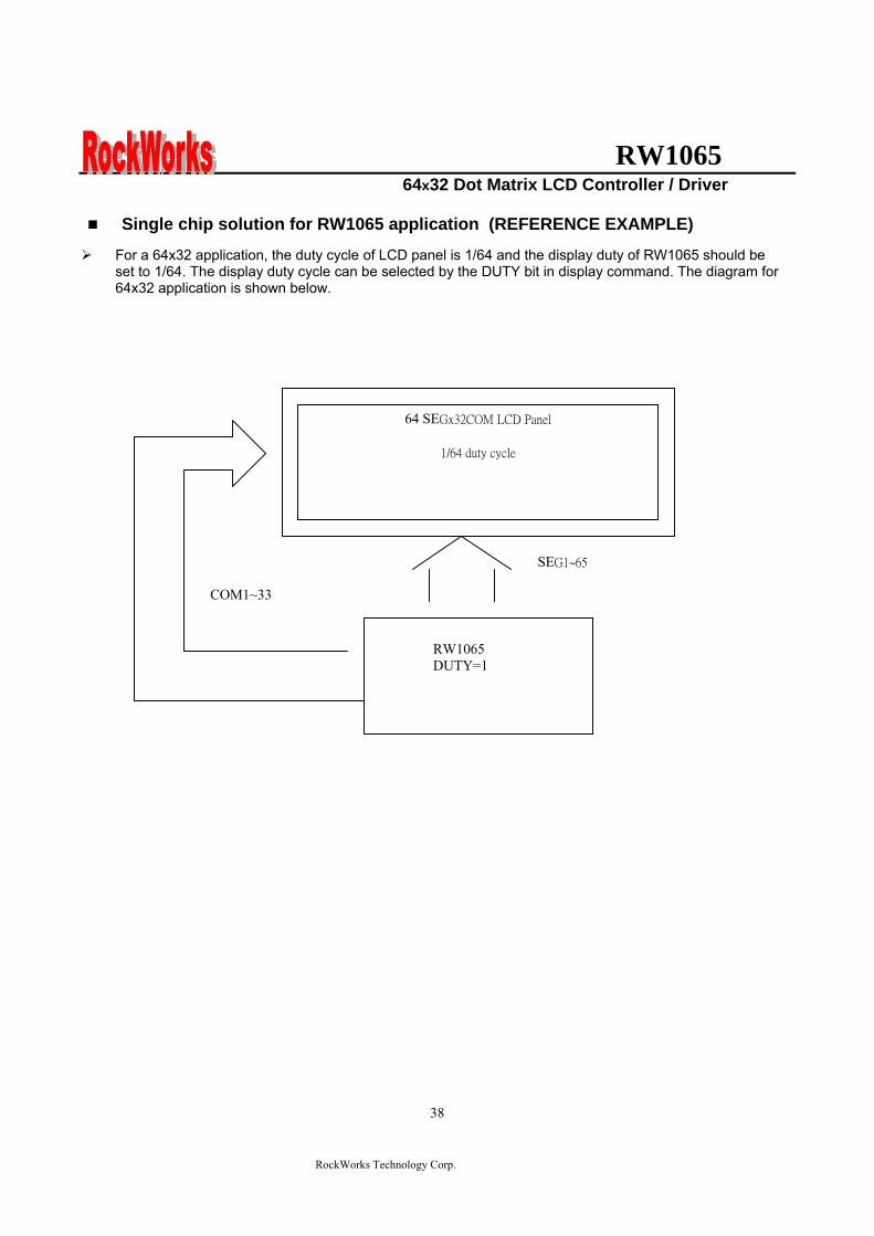
RW1065 64x32 Dot Matrix LCD Controller Driver
RockWorks Technology Corp
38
Single chip solution for RW1065 application (REFERENCE EXAMPLE)
For a 64x32 application the duty cycle of LCD panel is 164 and the display duty of RW1065 should be set to 164 The display duty cycle can be selected by the DUTY bit in display command The diagram for 64x32 application is shown below
64 SEGx32COM LCD Panel
164 duty cycle
RW1065 DUTY=1
COM1~33
SEG1~65
RW1065 64x32 Dot Matrix LCD Controller Driver
RockWorks Technology Corp
39
Using an adjustable resistor on the main board to adjust the contrast of liquid crystal display (REFERENCE EXAMPLE)
The schematic shows an adjustable resistor on main board that can adjust voltage level of V0
RW1065 64x32 Dot Matrix LCD Controller Driver
RockWorks Technology Corp
40
Package information (Please pay close attention to the information in this section Do not hesitate to consult with our sale representative if you have any question or concern)
In order to make better bonding yield for RW1065 please follow the tips and recommendations in this section In this section few tips about COB footprint style PCB layout and wire bonding will be discussed
The drawing in below shows the PCB footprint style which we recommend for RW1065 Pads array in
curve shape is easier for Al wire bonding Besides that a real size COB footprint for RW1065 is also shown in below RW1065 COB footprint is also available in powerpcb or protel format for design reference purpose
The ratio is 11
RW1065 64x32 Dot Matrix LCD Controller Driver
RockWorks Technology Corp
41
During COB footprint design there have some tips about footprint that the PCB designer should know The angle between bonding wire and vertical line should less than 45 Otherwise the wire shorts would become very easy to happen at fours corners of the chip
The angle between bonding wire and vertical line could be reduced by expanding the distance between pads array and the chip In addition reducing length in horizon direction of pads array could minimize the angle between bonding wire and vertical line The picture in below will help to illustrate this concept From the experiences COB footprint style affects the bonding yield
Bad Wires are too close to each other
The angle between bonding wire and vertical line is greater than 45
The angle between bonding wire and vertical line is less than 45
Wires are not too close to each other
Reducing length in horizon direction of pads array could minimize the angle between bonding wire and vertical line
The angle between bonding wire and vertical line could be reduced by expanding the distance between pads array and the chip
RW1065 64x32 Dot Matrix LCD Controller Driver
RockWorks Technology Corp
42
If the gap between pads of COB footprint is filled with solder mask coating it is difficult to bond Al wire to
the pads The top solder masks layer that overlap COB footprint area should be removed
Please use 1 mils diameter Al wire for RW1065 wire bonding
1 2 3 4 5 6
A
B
C
D
654321
D
C
B
A
Title
Number RevisionSize
C
Date 29-Aug-2007 Sheet of File D公司資料99seMyDesignddb Drawn By
RW1065
COM131
COM142
COM153
COM164
COM175
COM186
COM197
COM208
COM219
COM2210
COM2311
COM2412
COM2513
COM2614
COM2715
COM2816
COM2917
COM3018
COM3119
SEG
6320
SEG
6221
SEG
6122
SEG
6023
SEG
5924
SEG
5825
SEG
5726
SEG
5627
SEG
5528
SEG
5429
SEG
5330
SEG
5231
SEG
5132
SEG
5033
SEG
4934
SEG
4835
SEG
4736
SEG
4637
SEG
4538
SEG
4439
SEG
4340
SEG
4241
SEG
4142
SEG
4043
SEG
3944
SEG
3845
SEG
3746
SEG
3647
SEG
3548
SEG
3449
SEG
3350
SEG
3251
SEG
3152
SEG
3053
SEG
2954
SEG
2855
SEG
2756
SEG
2657
SEG
2558
SEG
2459
SEG
2360
SEG
2261
SEG
2162
SEG
2063
SEG
1964
SEG
1865
SEG
1766
SEG
1667
SEG
1568
SEG
1469
SEG13 70SEG12 71SEG11 72SEG10 73SEG9 74SEG8 75SEG7 76SEG6 77SEG5 78SEG4 79SEG3 80SEG2 81SEG1 82SEG0 83ADCP 84CLL 85
VSS
86D
087
D1
88D
289
D3
90D
491
D5
92D
693
D7
94C
S1B
P95
CS2
P96
ERD
P97
AO
P(R
S)98
RW
RP
99V
DD
100
RST
P10
1C
LSP
102
FRR
103
MSP
104
BS1
P10
5B
S0P
106
SHLP
107
VD
D2
108
CA
P2N
109
CA
P2P
110
CA
P1P
111
CA
P1N
112
CA
P3P
113
VO
UT
114
V0
115
VR
AB
116
V3
117
V2
118
V4
119
V1
120
CO
M0
121
CO
M1
122
CO
M2
123
CO
M3
124
CO
M4
125
CO
M5
126
CO
M6
127
CO
M7
128
CO
M8
129
CO
M9
130
CO
M10
131
CO
M11
132
CO
M12
133
4897x1902 um
IC1
RW1065
C9CAPR4
100R0603
R30R0603
C8
CAP
C7
CAP
R2
100R0603
R1
0R0603C6 22uf
R50R
R6300R
R7RES1
R8NC R9
100R0603
VDD
R10
NC
R11
100R0603
R12
100R0603
R13
NC
R14
100R0603
R15
NC
VDD
D0
D1
D2
D3
D4
D5
D6
D7
DB[07]
VDDC5
01uf0603
VD
D
CS2
P
123456789
1011121314151617181920
J1
CON20
C1201uf0603
R3951K0603
VDD
CAP Value1UF~22UF
2XPut C6C8 Short R1R3Open R2R4C7C93XPut C6C8C9 R4Short R1Open R2R3C74XOpen R1R3
BS0 BS1 Bias0 0
0 1
1 0
11
15 bias
16 bias
18 bias
19 bias
ADC=0 SEG0lt~column address 00Hnormal(default) ADC=1 SEG0lt~column address 3FHinverted
SHL=0 Normal COM0~gtCOM63(default)SHL=1 Reverse direction COM63~gtCOM0
R16100R0603
LCD PANEL 64X32RockWorks
RW1065 64X32
COM0-31 SEG0-63SHL=0 ADC=0
SHL=1COM31-0
ADC=1SEG63-0
if use single chip for 32 command displaythe display command must select 164 dutyDisplay panel must select 164 duty type
VO
UT
C3P
C1N
C1P
C2P
C2N
VDD2
ADC
SHL
BS0
BS1
CLLADC
V1
V2
V3
V4
VR
AB
V0
VO
UT
C3P
C1N
C1P
C2P
C2N
VD
D2
SHL
BS0
BS1
FRR
RST
P
RW
RS
E CS1
B
CS1
V0RSRWED0D1D2D3D4D5D6D7
RSTPAK
C4
22uf
RBRES1
RA1RES1
C2
22uf
C1
22uf
C3
22uf
C0
22uf
R20
100k0603
R21
100k0603
R17
200K0603
V1
V2
V3
V4 VRAB
V0
V0
OPTION
B
R18
300R0603
RA2RES1
VADJ
R19100R
R23 RES1R22 0R
R24
RES1
R25
0R
VDD
CS1BP
CS2P
CS1
CS1
R26
22R0603
R27
22R0603
C1047uf
C11
01uf
VSS_INVDD_IN
D1DIODE
FGND
鐵框地
VSS
VDD
R28 10RR29 10RR30 10RR31 10RR32 10RR33 10RR34 10RR35 10RR36 10RR37 10RR38 10R
VADJ
1 2 3 4 5 6
A
B
C
D
654321
D
C
B
A
Title
Number RevisionSize
C
Date 29-Aug-2007 Sheet of File D公司資料99seMyDesignddb Drawn By
RW1065
COM131
COM142
COM153
COM164
COM175
COM186
COM197
COM208
COM219
COM2210
COM2311
COM2412
COM2513
COM2614
COM2715
COM2816
COM2917
COM3018
COM3119
SEG
6320
SEG
6221
SEG
6122
SEG
6023
SEG
5924
SEG
5825
SEG
5726
SEG
5627
SEG
5528
SEG
5429
SEG
5330
SEG
5231
SEG
5132
SEG
5033
SEG
4934
SEG
4835
SEG
4736
SEG
4637
SEG
4538
SEG
4439
SEG
4340
SEG
4241
SEG
4142
SEG
4043
SEG
3944
SEG
3845
SEG
3746
SEG
3647
SEG
3548
SEG
3449
SEG
3350
SEG
3251
SEG
3152
SEG
3053
SEG
2954
SEG
2855
SEG
2756
SEG
2657
SEG
2558
SEG
2459
SEG
2360
SEG
2261
SEG
2162
SEG
2063
SEG
1964
SEG
1865
SEG
1766
SEG
1667
SEG
1568
SEG
1469
SEG13 70SEG12 71SEG11 72SEG10 73SEG9 74SEG8 75SEG7 76SEG6 77SEG5 78SEG4 79SEG3 80SEG2 81SEG1 82SEG0 83ADCP 84CLL 85
VSS
86D
087
D1
88D
289
D3
90D
491
D5
92D
693
D7
94C
S1B
P95
CS2
P96
ERD
P97
AO
P(R
S)98
RW
RP
99V
DD
100
RST
P10
1C
LSP
102
FRR
103
MSP
104
BS1
P10
5B
S0P
106
SHLP
107
VD
D2
108
CA
P2N
109
CA
P2P
110
CA
P1P
111
CA
P1N
112
CA
P3P
113
VO
UT
114
V0
115
VR
AB
116
V3
117
V2
118
V4
119
V1
120
CO
M0
121
CO
M1
122
CO
M2
123
CO
M3
124
CO
M4
125
CO
M5
126
CO
M6
127
CO
M7
128
CO
M8
129
CO
M9
130
CO
M10
131
CO
M11
132
CO
M12
133
4897x1902 um
IC1
RW1065 Master
RW1065
COM131
COM142
COM153
COM164
COM175
COM186
COM197
COM208
COM219
COM2210
COM2311
COM2412
COM2513
COM2614
COM2715
COM2816
COM2917
COM3018
COM3119
SEG
6320
SEG
6221
SEG
6122
SEG
6023
SEG
5924
SEG
5825
SEG
5726
SEG
5627
SEG
5528
SEG
5429
SEG
5330
SEG
5231
SEG
5132
SEG
5033
SEG
4934
SEG
4835
SEG
4736
SEG
4637
SEG
4538
SEG
4439
SEG
4340
SEG
4241
SEG
4142
SEG
4043
SEG
3944
SEG
3845
SEG
3746
SEG
3647
SEG
3548
SEG
3449
SEG
3350
SEG
3251
SEG
3152
SEG
3053
SEG
2954
SEG
2855
SEG
2756
SEG
2657
SEG
2558
SEG
2459
SEG
2360
SEG
2261
SEG
2162
SEG
2063
SEG
1964
SEG
1865
SEG
1766
SEG
1667
SEG
1568
SEG
1469
SEG13 70SEG12 71SEG11 72SEG10 73SEG9 74SEG8 75SEG7 76SEG6 77SEG5 78SEG4 79SEG3 80SEG2 81SEG1 82SEG0 83ADCP 84CLL 85
VSS
86D
087
D1
88D
289
D3
90D
491
D5
92D
693
D7
94C
S1B
P95
CS2
P96
ERD
P97
AO
P(R
S)98
RW
RP
99V
DD
100
RST
P10
1C
LSP
102
FRR
103
MSP
104
BS1
P10
5B
S0P
106
SHLP
107
VD
D2
108
CA
P2N
109
CA
P2P
110
CA
P1P
111
CA
P1N
112
CA
P3P
113
VO
UT
114
V0
115
VR
AB
116
V3
117
V2
118
V4
119
V1
120
CO
M0
121
CO
M1
122
CO
M2
123
CO
M3
124
CO
M4
125
CO
M5
126
CO
M6
127
CO
M7
128
CO
M8
129
CO
M9
130
CO
M10
131
CO
M11
132
CO
M12
133
4897x1902 um
IC2
RW1065 Slave
C4
22uf
RBRES1
RA1RES1
C2
22uf
C1
22uf
C3
22uf
C0
22ufC9CAPR4
100R0603
R30R0603
C8
CAP
C7
CAP
R2
100R0603
R1
0R0603C6 22uf
R50R0603
R6300R0603
R7RES1
R8NC R9
100R0603
VDD
R10
NC
R11
100R0603
R12
NC
R13
100R0603
R14
100R0603
R15
NC
R16
100R0603
R17
NC
VDD
D0
D1
D2
D3
D4
D5
D6
D7
D0
D1
D2
D3
D4
D5
D6
D7
DB[07] DB[07]
VDDC10
01uf0603
VD
D
IC1_
CS2
P
VDD
IC2_
CS2
P
VD
D
C11
01uf0603
VSS
VSS
LCD PANEL 128X64
Master COM0-31 Slave COM32-63
Master SEG0-63 Slave SEG64-127
123456789
1011121314151617181920
J1
CON20
Master Slave
CAP Value1UF~22UF
2XPut C6C8 Short R1R3Open R2R4C7C93XPut C6C8C9 R4Short R1Open R2R3C74XOpen R1R3
RockWorksRW1065 128x64
BS0 BS1 Bias0 0
0 1
1 0
11
15 bias
16 bias
18 bias
19 bias
ADC=0 SEG0lt~column address 00Hnormal(default) ADC=1 SEG0lt~column address 3FHinverted
SHL=0 Normal COM0~gtCOM63(default)SHL=1 Reverse direction COM63~gtCOM0Both Master and Slave should set identical SHL value
SHL=0 SHL=0
ADC=0 ADC=0
Slave COM31-0
Slave SEG127-64
SHL=1
ADC=1
SHL=1Master COM63-32
ADC=1Master SEG63-0
R18100R0603
R22
100k0603
R23
100k0603
C501uF0603
R4551K0603
VDD
R19
200K0603
ADC1
ADC2
SHL
BS0
BS1
VDD2
V1
V2
V3
V4 VRAB
V0
V0V
OU
T
C3P
C1N
C1P
C2P
C2N
V1
V2
V3
V4
VR
AB
V0
VO
UT
C3P
C1N
C1P
C2P
C2N
VD
D2
SHL
BS0
BS1
FRR
RST
P
RW
RS
E IC1_
CS1
BP
V1
V2
V3
V4
VR
AB
V0
VO
UT
VD
D2
SHL
BS0
BS1
FRR
RST
P
RW
RS
E IC2_
CS1
BP
CLLADC1
CLLADC2
RSTP
CS1CS2
V0RSRWED0D1D2D3D4D5D6D7
AK
OPTION
R20
300R0603
RA2RES1
VADJ
R21
100R
B
R25 RESR24 0R
R26 RES R27 0RVDD
IC1_CS1BP
IC1_CS2P
CS1
CS1
R28 0R R29 RES
R30 RES R31 0R
IC2_CS1BP
IC2_CS2P
CS2
CS2
R32
22R0603
R33
22R0603
C1001uf
C11
47uf
D1DIODE
FGND
鐵框地
VSS
VDD
R34 10RR35 10RR36 10RR37 10RR38 10RR39 10RR40 10RR41 10RR42 10RR43 10RR44 10R
VSS_INVDD_IN
VADJ
VDD
1 2 3 4 5 6 7 8
A
B
C
D
87654321
D
C
B
A
Title
Number RevisionSize
D
Date 29-Aug-2007 Sheet of File D公司資料 99seMyDesignddb Drawn By
C422uf
RBRES1
RA1RES1
C3
22uf
C2
22uf
C1
22uf
C0
22ufC9CAPR4
100R0603
R30R0603
C8
CAP
C7
CAP
R2
100R0603
R1
0R0603C6 22uf
R220R0603
R23300R0603
R24RES1
R39
NCR40
100 ohm0603
VDD
R41
NC
R42
100 ohm0603
R43
NC
R44
100 ohm0603
R45
NC
R46
100 ohm0603
R47
100 ohm0603
R48
NC
R49
100 ohm0603
R50
NC
VDDCAP Value1UF~22UF
2XPut C6C8 Short R1R3Open R2R4C7C93XPut C6C8C9 R4Short R1Open R2R3C74XOpen R1R3
BS0 BS1 Bias0 0
0 1
1 0
11
15 bias
16 bias
18 bias
19 bias
ADC=0 SEG0lt~column address 00Hnormal(default)
ADC=1 SEG0lt~column address 3FHinverted
SHL=0 Normal COM0~gtCOM63(default)SHL=1 Reverse direction COM63~gtCOM0Both Master and Slave should set identical SHL value
R7
100k0603
R8
100k0603
V1
V2
V3
V4
V0
VRAB
V0
R5
200K
VDD2
VO
UT
C3P
C1N
C1P
C2P
C2N
ADC1
ADC2
ADC3
SHL
BS0
BS1
CS1CS2CS3
V0RSRWED0D1D2D3D4D5D6D7
RSTP
R3851K0603
C5
01uF
VDD
OPTION
R6
300R0603R9100R
RA2RES1
VADJ
RW1065
COM131
COM142
COM153
COM164
COM175
COM186
COM197
COM208
COM219
COM2210
COM2311
COM2412
COM2513
COM2614
COM2715
COM2816
COM2917
COM3018
COM3119
SEG
6320
SEG
6221
SEG
6122
SEG
6023
SEG
5924
SEG
5825
SEG
5726
SEG
5627
SEG
5528
SEG
5429
SEG
5330
SEG
5231
SEG
5132
SEG
5033
SEG
4934
SEG
4835
SEG
4736
SEG
4637
SEG
4538
SEG
4439
SEG
4340
SEG
4241
SEG
4142
SEG
4043
SEG
3944
SEG
3845
SEG
3746
SEG
3647
SEG
3548
SEG
3449
SEG
3350
SEG
3251
SEG
3152
SEG
3053
SEG
2954
SEG
2855
SEG
2756
SEG
2657
SEG
2558
SEG
2459
SEG
2360
SEG
2261
SEG
2162
SEG
2063
SEG
1964
SEG
1865
SEG
1766
SEG
1667
SEG
1568
SEG
1469
SEG13 70SEG12 71SEG11 72SEG10 73SEG9 74SEG8 75SEG7 76SEG6 77SEG5 78SEG4 79SEG3 80SEG2 81SEG1 82SEG0 83ADCP 84CLL 85
VSS
86D
087
D1
88D
289
D3
90D
491
D5
92D
693
D7
94C
S1B
P95
CS2
P96
ERD
P97
AO
P(R
S)98
RW
RP
99V
DD
100
RST
P10
1C
LSP
102
FRR
103
MSP
104
BS1
P10
5B
S0P
106
SHLP
107
VD
D2
108
CA
P2N
109
CA
P2P
110
CA
P1P
111
CA
P1N
112
CA
P3P
113
VO
UT
114
V0
115
VR
AB
116
V3
117
V2
118
V4
119
V1
120
CO
M0
121
CO
M1
122
CO
M2
123
CO
M3
124
CO
M4
125
CO
M5
126
CO
M6
127
CO
M7
128
CO
M8
129
CO
M9
130
CO
M10
131
CO
M11
132
CO
M12
133
4897x1902 um
IC1
RW1065 Master
RW1065
COM131
COM142
COM153
COM164
COM175
COM186
COM197
COM208
COM219
COM2210
COM2311
COM2412
COM2513
COM2614
COM2715
COM2816
COM2917
COM3018
COM3119
SEG
6320
SEG
6221
SEG
6122
SEG
6023
SEG
5924
SEG
5825
SEG
5726
SEG
5627
SEG
5528
SEG
5429
SEG
5330
SEG
5231
SEG
5132
SEG
5033
SEG
4934
SEG
4835
SEG
4736
SEG
4637
SEG
4538
SEG
4439
SEG
4340
SEG
4241
SEG
4142
SEG
4043
SEG
3944
SEG
3845
SEG
3746
SEG
3647
SEG
3548
SEG
3449
SEG
3350
SEG
3251
SEG
3152
SEG
3053
SEG
2954
SEG
2855
SEG
2756
SEG
2657
SEG
2558
SEG
2459
SEG
2360
SEG
2261
SEG
2162
SEG
2063
SEG
1964
SEG
1865
SEG
1766
SEG
1667
SEG
1568
SEG
1469
SEG13 70SEG12 71SEG11 72SEG10 73SEG9 74SEG8 75SEG7 76SEG6 77SEG5 78SEG4 79SEG3 80SEG2 81SEG1 82SEG0 83ADCP 84CLL 85
VSS
86D
087
D1
88D
289
D3
90D
491
D5
92D
693
D7
94C
S1B
P95
CS2
P96
ERD
P97
AO
P(R
S)98
RW
RP
99V
DD
100
RST
P10
1C
LSP
102
FRR
103
MSP
104
BS1
P10
5B
S0P
106
SHLP
107
VD
D2
108
CA
P2N
109
CA
P2P
110
CA
P1P
111
CA
P1N
112
CA
P3P
113
VO
UT
114
V0
115
VR
AB
116
V3
117
V2
118
V4
119
V1
120
CO
M0
121
CO
M1
122
CO
M2
123
CO
M3
124
CO
M4
125
CO
M5
126
CO
M6
127
CO
M7
128
CO
M8
129
CO
M9
130
CO
M10
131
CO
M11
132
CO
M12
133
4897x1902 um
IC2
RW1065 Slave
D0
D1
D2
D3
D4
D5
D6
D7
D0
D1
D2
D3
D4
D5
D6
D7
DB[07] DB[07]
VDDC8
01uf0603
VD
D
VDD
VD
D
C9
01uf0603
VSS
VSS
LCD PANEL 192X64
Master COM0-31 Slave COM32-63
Master SEG0-63 Slave SEG64-127
Master Slave
RockWorksRW1065 192x64
RW1065
COM131
COM142
COM153
COM164
COM175
COM186
COM197
COM208
COM219
COM2210
COM2311
COM2412
COM2513
COM2614
COM2715
COM2816
COM2917
COM3018
COM3119
SEG
6320
SEG
6221
SEG
6122
SEG
6023
SEG
5924
SEG
5825
SEG
5726
SEG
5627
SEG
5528
SEG
5429
SEG
5330
SEG
5231
SEG
5132
SEG
5033
SEG
4934
SEG
4835
SEG
4736
SEG
4637
SEG
4538
SEG
4439
SEG
4340
SEG
4241
SEG
4142
SEG
4043
SEG
3944
SEG
3845
SEG
3746
SEG
3647
SEG
3548
SEG
3449
SEG
3350
SEG
3251
SEG
3152
SEG
3053
SEG
2954
SEG
2855
SEG
2756
SEG
2657
SEG
2558
SEG
2459
SEG
2360
SEG
2261
SEG
2162
SEG
2063
SEG
1964
SEG
1865
SEG
1766
SEG
1667
SEG
1568
SEG
1469
SEG13 70SEG12 71SEG11 72SEG10 73SEG9 74SEG8 75SEG7 76SEG6 77SEG5 78SEG4 79SEG3 80SEG2 81SEG1 82SEG0 83ADCP 84CLL 85
VSS
86D
087
D1
88D
289
D3
90D
491
D5
92D
693
D7
94C
S1B
P95
CS2
P96
ERD
P97
AO
P(R
S)98
RW
RP
99V
DD
100
RST
P10
1C
LSP
102
FRR
103
MSP
104
BS1
P10
5B
S0P
106
SHLP
107
VD
D2
108
CA
P2N
109
CA
P2P
110
CA
P1P
111
CA
P1N
112
CA
P3P
113
VO
UT
114
V0
115
VR
AB
116
V3
117
V2
118
V4
119
V1
120
CO
M0
121
CO
M1
122
CO
M2
123
CO
M3
124
CO
M4
125
CO
M5
126
CO
M6
127
CO
M7
128
CO
M8
129
CO
M9
130
CO
M10
131
CO
M11
132
CO
M12
133
4897x1902 um
IC3
RW1065 Slave
D0
D1
D2
D3
D4
D5
D6
D7
DB[07]
VSS
VSS
VDD
VD
D
C10
01uf0603
Slave SEG128-192
Slave
SHL=0 SHL=0
Master COM63-32SHL=1 SHL=1
Slave COM31-0ADC=0 ADC=0 ADC=0
ADC=1 ADC=1 ADC=1Master SEG63-0 Slave SEG127-64 Slave SEG192-128
R50100R0603
V1
V2
V3
V4
VR
AB
V0
VO
UT
C3P
C1N
C1P
C2P
C2N
VD
D2
SHL
BS0
BS1
FRR
RST
P
RW
RS
E V1
V2
V3
V4
VR
AB
V0
VO
UT
VD
D2
SHL
BS0
BS1
FRR
RST
P
RW
RS
E V1
V2
V3
V4
VR
AB
V0
VO
UT
VD
D2
SHL
BS0
BS1
FRR
RST
P
RW
RS
E
CLL CLL CLLADC1 ADC2 ADC3
R25 10RR26 10RR27 10RR28 10RR29 10RR30 10RR31 10RR32 10RR33 10RR34 10RR35 10R
R36
22R0603
D1DIODE
R3722R0603
C647uf
C701uf
VSS_INVDD_IN
VSS
VDD
VADJ
123456789
101112131415161718192021222324
J1
CON24
AK
FGND
鐵框地
IC1_
CS1
BP
IC1_
CS2
P
IC2_
CS2
PIC
2_C
S1B
P
IC3_
CS1
BP
IC3_
CS2
B
R10 0R R11 RES
R12 RES R13 0RVDD
IC1_CS2B
IC1_CS1BPCS1
CS1
R14 0R R15 RES
R16 RES R17 0RVDDIC2_CS2B
IC2_CS1BPCS2
CS2
R18 0R R19 RES
R20 RES R21 0RVDDIC3_CS2B
IC3_CS1BPCS3
CS3
B
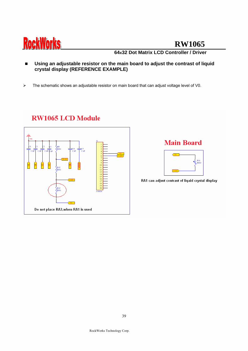
RW1065 64x32 Dot Matrix LCD Controller Driver
RockWorks Technology Corp
39
Using an adjustable resistor on the main board to adjust the contrast of liquid crystal display (REFERENCE EXAMPLE)
The schematic shows an adjustable resistor on main board that can adjust voltage level of V0
RW1065 64x32 Dot Matrix LCD Controller Driver
RockWorks Technology Corp
40
Package information (Please pay close attention to the information in this section Do not hesitate to consult with our sale representative if you have any question or concern)
In order to make better bonding yield for RW1065 please follow the tips and recommendations in this section In this section few tips about COB footprint style PCB layout and wire bonding will be discussed
The drawing in below shows the PCB footprint style which we recommend for RW1065 Pads array in
curve shape is easier for Al wire bonding Besides that a real size COB footprint for RW1065 is also shown in below RW1065 COB footprint is also available in powerpcb or protel format for design reference purpose
The ratio is 11
RW1065 64x32 Dot Matrix LCD Controller Driver
RockWorks Technology Corp
41
During COB footprint design there have some tips about footprint that the PCB designer should know The angle between bonding wire and vertical line should less than 45 Otherwise the wire shorts would become very easy to happen at fours corners of the chip
The angle between bonding wire and vertical line could be reduced by expanding the distance between pads array and the chip In addition reducing length in horizon direction of pads array could minimize the angle between bonding wire and vertical line The picture in below will help to illustrate this concept From the experiences COB footprint style affects the bonding yield
Bad Wires are too close to each other
The angle between bonding wire and vertical line is greater than 45
The angle between bonding wire and vertical line is less than 45
Wires are not too close to each other
Reducing length in horizon direction of pads array could minimize the angle between bonding wire and vertical line
The angle between bonding wire and vertical line could be reduced by expanding the distance between pads array and the chip
RW1065 64x32 Dot Matrix LCD Controller Driver
RockWorks Technology Corp
42
If the gap between pads of COB footprint is filled with solder mask coating it is difficult to bond Al wire to
the pads The top solder masks layer that overlap COB footprint area should be removed
Please use 1 mils diameter Al wire for RW1065 wire bonding
1 2 3 4 5 6
A
B
C
D
654321
D
C
B
A
Title
Number RevisionSize
C
Date 29-Aug-2007 Sheet of File D公司資料99seMyDesignddb Drawn By
RW1065
COM131
COM142
COM153
COM164
COM175
COM186
COM197
COM208
COM219
COM2210
COM2311
COM2412
COM2513
COM2614
COM2715
COM2816
COM2917
COM3018
COM3119
SEG
6320
SEG
6221
SEG
6122
SEG
6023
SEG
5924
SEG
5825
SEG
5726
SEG
5627
SEG
5528
SEG
5429
SEG
5330
SEG
5231
SEG
5132
SEG
5033
SEG
4934
SEG
4835
SEG
4736
SEG
4637
SEG
4538
SEG
4439
SEG
4340
SEG
4241
SEG
4142
SEG
4043
SEG
3944
SEG
3845
SEG
3746
SEG
3647
SEG
3548
SEG
3449
SEG
3350
SEG
3251
SEG
3152
SEG
3053
SEG
2954
SEG
2855
SEG
2756
SEG
2657
SEG
2558
SEG
2459
SEG
2360
SEG
2261
SEG
2162
SEG
2063
SEG
1964
SEG
1865
SEG
1766
SEG
1667
SEG
1568
SEG
1469
SEG13 70SEG12 71SEG11 72SEG10 73SEG9 74SEG8 75SEG7 76SEG6 77SEG5 78SEG4 79SEG3 80SEG2 81SEG1 82SEG0 83ADCP 84CLL 85
VSS
86D
087
D1
88D
289
D3
90D
491
D5
92D
693
D7
94C
S1B
P95
CS2
P96
ERD
P97
AO
P(R
S)98
RW
RP
99V
DD
100
RST
P10
1C
LSP
102
FRR
103
MSP
104
BS1
P10
5B
S0P
106
SHLP
107
VD
D2
108
CA
P2N
109
CA
P2P
110
CA
P1P
111
CA
P1N
112
CA
P3P
113
VO
UT
114
V0
115
VR
AB
116
V3
117
V2
118
V4
119
V1
120
CO
M0
121
CO
M1
122
CO
M2
123
CO
M3
124
CO
M4
125
CO
M5
126
CO
M6
127
CO
M7
128
CO
M8
129
CO
M9
130
CO
M10
131
CO
M11
132
CO
M12
133
4897x1902 um
IC1
RW1065
C9CAPR4
100R0603
R30R0603
C8
CAP
C7
CAP
R2
100R0603
R1
0R0603C6 22uf
R50R
R6300R
R7RES1
R8NC R9
100R0603
VDD
R10
NC
R11
100R0603
R12
100R0603
R13
NC
R14
100R0603
R15
NC
VDD
D0
D1
D2
D3
D4
D5
D6
D7
DB[07]
VDDC5
01uf0603
VD
D
CS2
P
123456789
1011121314151617181920
J1
CON20
C1201uf0603
R3951K0603
VDD
CAP Value1UF~22UF
2XPut C6C8 Short R1R3Open R2R4C7C93XPut C6C8C9 R4Short R1Open R2R3C74XOpen R1R3
BS0 BS1 Bias0 0
0 1
1 0
11
15 bias
16 bias
18 bias
19 bias
ADC=0 SEG0lt~column address 00Hnormal(default) ADC=1 SEG0lt~column address 3FHinverted
SHL=0 Normal COM0~gtCOM63(default)SHL=1 Reverse direction COM63~gtCOM0
R16100R0603
LCD PANEL 64X32RockWorks
RW1065 64X32
COM0-31 SEG0-63SHL=0 ADC=0
SHL=1COM31-0
ADC=1SEG63-0
if use single chip for 32 command displaythe display command must select 164 dutyDisplay panel must select 164 duty type
VO
UT
C3P
C1N
C1P
C2P
C2N
VDD2
ADC
SHL
BS0
BS1
CLLADC
V1
V2
V3
V4
VR
AB
V0
VO
UT
C3P
C1N
C1P
C2P
C2N
VD
D2
SHL
BS0
BS1
FRR
RST
P
RW
RS
E CS1
B
CS1
V0RSRWED0D1D2D3D4D5D6D7
RSTPAK
C4
22uf
RBRES1
RA1RES1
C2
22uf
C1
22uf
C3
22uf
C0
22uf
R20
100k0603
R21
100k0603
R17
200K0603
V1
V2
V3
V4 VRAB
V0
V0
OPTION
B
R18
300R0603
RA2RES1
VADJ
R19100R
R23 RES1R22 0R
R24
RES1
R25
0R
VDD
CS1BP
CS2P
CS1
CS1
R26
22R0603
R27
22R0603
C1047uf
C11
01uf
VSS_INVDD_IN
D1DIODE
FGND
鐵框地
VSS
VDD
R28 10RR29 10RR30 10RR31 10RR32 10RR33 10RR34 10RR35 10RR36 10RR37 10RR38 10R
VADJ
1 2 3 4 5 6
A
B
C
D
654321
D
C
B
A
Title
Number RevisionSize
C
Date 29-Aug-2007 Sheet of File D公司資料99seMyDesignddb Drawn By
RW1065
COM131
COM142
COM153
COM164
COM175
COM186
COM197
COM208
COM219
COM2210
COM2311
COM2412
COM2513
COM2614
COM2715
COM2816
COM2917
COM3018
COM3119
SEG
6320
SEG
6221
SEG
6122
SEG
6023
SEG
5924
SEG
5825
SEG
5726
SEG
5627
SEG
5528
SEG
5429
SEG
5330
SEG
5231
SEG
5132
SEG
5033
SEG
4934
SEG
4835
SEG
4736
SEG
4637
SEG
4538
SEG
4439
SEG
4340
SEG
4241
SEG
4142
SEG
4043
SEG
3944
SEG
3845
SEG
3746
SEG
3647
SEG
3548
SEG
3449
SEG
3350
SEG
3251
SEG
3152
SEG
3053
SEG
2954
SEG
2855
SEG
2756
SEG
2657
SEG
2558
SEG
2459
SEG
2360
SEG
2261
SEG
2162
SEG
2063
SEG
1964
SEG
1865
SEG
1766
SEG
1667
SEG
1568
SEG
1469
SEG13 70SEG12 71SEG11 72SEG10 73SEG9 74SEG8 75SEG7 76SEG6 77SEG5 78SEG4 79SEG3 80SEG2 81SEG1 82SEG0 83ADCP 84CLL 85
VSS
86D
087
D1
88D
289
D3
90D
491
D5
92D
693
D7
94C
S1B
P95
CS2
P96
ERD
P97
AO
P(R
S)98
RW
RP
99V
DD
100
RST
P10
1C
LSP
102
FRR
103
MSP
104
BS1
P10
5B
S0P
106
SHLP
107
VD
D2
108
CA
P2N
109
CA
P2P
110
CA
P1P
111
CA
P1N
112
CA
P3P
113
VO
UT
114
V0
115
VR
AB
116
V3
117
V2
118
V4
119
V1
120
CO
M0
121
CO
M1
122
CO
M2
123
CO
M3
124
CO
M4
125
CO
M5
126
CO
M6
127
CO
M7
128
CO
M8
129
CO
M9
130
CO
M10
131
CO
M11
132
CO
M12
133
4897x1902 um
IC1
RW1065 Master
RW1065
COM131
COM142
COM153
COM164
COM175
COM186
COM197
COM208
COM219
COM2210
COM2311
COM2412
COM2513
COM2614
COM2715
COM2816
COM2917
COM3018
COM3119
SEG
6320
SEG
6221
SEG
6122
SEG
6023
SEG
5924
SEG
5825
SEG
5726
SEG
5627
SEG
5528
SEG
5429
SEG
5330
SEG
5231
SEG
5132
SEG
5033
SEG
4934
SEG
4835
SEG
4736
SEG
4637
SEG
4538
SEG
4439
SEG
4340
SEG
4241
SEG
4142
SEG
4043
SEG
3944
SEG
3845
SEG
3746
SEG
3647
SEG
3548
SEG
3449
SEG
3350
SEG
3251
SEG
3152
SEG
3053
SEG
2954
SEG
2855
SEG
2756
SEG
2657
SEG
2558
SEG
2459
SEG
2360
SEG
2261
SEG
2162
SEG
2063
SEG
1964
SEG
1865
SEG
1766
SEG
1667
SEG
1568
SEG
1469
SEG13 70SEG12 71SEG11 72SEG10 73SEG9 74SEG8 75SEG7 76SEG6 77SEG5 78SEG4 79SEG3 80SEG2 81SEG1 82SEG0 83ADCP 84CLL 85
VSS
86D
087
D1
88D
289
D3
90D
491
D5
92D
693
D7
94C
S1B
P95
CS2
P96
ERD
P97
AO
P(R
S)98
RW
RP
99V
DD
100
RST
P10
1C
LSP
102
FRR
103
MSP
104
BS1
P10
5B
S0P
106
SHLP
107
VD
D2
108
CA
P2N
109
CA
P2P
110
CA
P1P
111
CA
P1N
112
CA
P3P
113
VO
UT
114
V0
115
VR
AB
116
V3
117
V2
118
V4
119
V1
120
CO
M0
121
CO
M1
122
CO
M2
123
CO
M3
124
CO
M4
125
CO
M5
126
CO
M6
127
CO
M7
128
CO
M8
129
CO
M9
130
CO
M10
131
CO
M11
132
CO
M12
133
4897x1902 um
IC2
RW1065 Slave
C4
22uf
RBRES1
RA1RES1
C2
22uf
C1
22uf
C3
22uf
C0
22ufC9CAPR4
100R0603
R30R0603
C8
CAP
C7
CAP
R2
100R0603
R1
0R0603C6 22uf
R50R0603
R6300R0603
R7RES1
R8NC R9
100R0603
VDD
R10
NC
R11
100R0603
R12
NC
R13
100R0603
R14
100R0603
R15
NC
R16
100R0603
R17
NC
VDD
D0
D1
D2
D3
D4
D5
D6
D7
D0
D1
D2
D3
D4
D5
D6
D7
DB[07] DB[07]
VDDC10
01uf0603
VD
D
IC1_
CS2
P
VDD
IC2_
CS2
P
VD
D
C11
01uf0603
VSS
VSS
LCD PANEL 128X64
Master COM0-31 Slave COM32-63
Master SEG0-63 Slave SEG64-127
123456789
1011121314151617181920
J1
CON20
Master Slave
CAP Value1UF~22UF
2XPut C6C8 Short R1R3Open R2R4C7C93XPut C6C8C9 R4Short R1Open R2R3C74XOpen R1R3
RockWorksRW1065 128x64
BS0 BS1 Bias0 0
0 1
1 0
11
15 bias
16 bias
18 bias
19 bias
ADC=0 SEG0lt~column address 00Hnormal(default) ADC=1 SEG0lt~column address 3FHinverted
SHL=0 Normal COM0~gtCOM63(default)SHL=1 Reverse direction COM63~gtCOM0Both Master and Slave should set identical SHL value
SHL=0 SHL=0
ADC=0 ADC=0
Slave COM31-0
Slave SEG127-64
SHL=1
ADC=1
SHL=1Master COM63-32
ADC=1Master SEG63-0
R18100R0603
R22
100k0603
R23
100k0603
C501uF0603
R4551K0603
VDD
R19
200K0603
ADC1
ADC2
SHL
BS0
BS1
VDD2
V1
V2
V3
V4 VRAB
V0
V0V
OU
T
C3P
C1N
C1P
C2P
C2N
V1
V2
V3
V4
VR
AB
V0
VO
UT
C3P
C1N
C1P
C2P
C2N
VD
D2
SHL
BS0
BS1
FRR
RST
P
RW
RS
E IC1_
CS1
BP
V1
V2
V3
V4
VR
AB
V0
VO
UT
VD
D2
SHL
BS0
BS1
FRR
RST
P
RW
RS
E IC2_
CS1
BP
CLLADC1
CLLADC2
RSTP
CS1CS2
V0RSRWED0D1D2D3D4D5D6D7
AK
OPTION
R20
300R0603
RA2RES1
VADJ
R21
100R
B
R25 RESR24 0R
R26 RES R27 0RVDD
IC1_CS1BP
IC1_CS2P
CS1
CS1
R28 0R R29 RES
R30 RES R31 0R
IC2_CS1BP
IC2_CS2P
CS2
CS2
R32
22R0603
R33
22R0603
C1001uf
C11
47uf
D1DIODE
FGND
鐵框地
VSS
VDD
R34 10RR35 10RR36 10RR37 10RR38 10RR39 10RR40 10RR41 10RR42 10RR43 10RR44 10R
VSS_INVDD_IN
VADJ
VDD
1 2 3 4 5 6 7 8
A
B
C
D
87654321
D
C
B
A
Title
Number RevisionSize
D
Date 29-Aug-2007 Sheet of File D公司資料 99seMyDesignddb Drawn By
C422uf
RBRES1
RA1RES1
C3
22uf
C2
22uf
C1
22uf
C0
22ufC9CAPR4
100R0603
R30R0603
C8
CAP
C7
CAP
R2
100R0603
R1
0R0603C6 22uf
R220R0603
R23300R0603
R24RES1
R39
NCR40
100 ohm0603
VDD
R41
NC
R42
100 ohm0603
R43
NC
R44
100 ohm0603
R45
NC
R46
100 ohm0603
R47
100 ohm0603
R48
NC
R49
100 ohm0603
R50
NC
VDDCAP Value1UF~22UF
2XPut C6C8 Short R1R3Open R2R4C7C93XPut C6C8C9 R4Short R1Open R2R3C74XOpen R1R3
BS0 BS1 Bias0 0
0 1
1 0
11
15 bias
16 bias
18 bias
19 bias
ADC=0 SEG0lt~column address 00Hnormal(default)
ADC=1 SEG0lt~column address 3FHinverted
SHL=0 Normal COM0~gtCOM63(default)SHL=1 Reverse direction COM63~gtCOM0Both Master and Slave should set identical SHL value
R7
100k0603
R8
100k0603
V1
V2
V3
V4
V0
VRAB
V0
R5
200K
VDD2
VO
UT
C3P
C1N
C1P
C2P
C2N
ADC1
ADC2
ADC3
SHL
BS0
BS1
CS1CS2CS3
V0RSRWED0D1D2D3D4D5D6D7
RSTP
R3851K0603
C5
01uF
VDD
OPTION
R6
300R0603R9100R
RA2RES1
VADJ
RW1065
COM131
COM142
COM153
COM164
COM175
COM186
COM197
COM208
COM219
COM2210
COM2311
COM2412
COM2513
COM2614
COM2715
COM2816
COM2917
COM3018
COM3119
SEG
6320
SEG
6221
SEG
6122
SEG
6023
SEG
5924
SEG
5825
SEG
5726
SEG
5627
SEG
5528
SEG
5429
SEG
5330
SEG
5231
SEG
5132
SEG
5033
SEG
4934
SEG
4835
SEG
4736
SEG
4637
SEG
4538
SEG
4439
SEG
4340
SEG
4241
SEG
4142
SEG
4043
SEG
3944
SEG
3845
SEG
3746
SEG
3647
SEG
3548
SEG
3449
SEG
3350
SEG
3251
SEG
3152
SEG
3053
SEG
2954
SEG
2855
SEG
2756
SEG
2657
SEG
2558
SEG
2459
SEG
2360
SEG
2261
SEG
2162
SEG
2063
SEG
1964
SEG
1865
SEG
1766
SEG
1667
SEG
1568
SEG
1469
SEG13 70SEG12 71SEG11 72SEG10 73SEG9 74SEG8 75SEG7 76SEG6 77SEG5 78SEG4 79SEG3 80SEG2 81SEG1 82SEG0 83ADCP 84CLL 85
VSS
86D
087
D1
88D
289
D3
90D
491
D5
92D
693
D7
94C
S1B
P95
CS2
P96
ERD
P97
AO
P(R
S)98
RW
RP
99V
DD
100
RST
P10
1C
LSP
102
FRR
103
MSP
104
BS1
P10
5B
S0P
106
SHLP
107
VD
D2
108
CA
P2N
109
CA
P2P
110
CA
P1P
111
CA
P1N
112
CA
P3P
113
VO
UT
114
V0
115
VR
AB
116
V3
117
V2
118
V4
119
V1
120
CO
M0
121
CO
M1
122
CO
M2
123
CO
M3
124
CO
M4
125
CO
M5
126
CO
M6
127
CO
M7
128
CO
M8
129
CO
M9
130
CO
M10
131
CO
M11
132
CO
M12
133
4897x1902 um
IC1
RW1065 Master
RW1065
COM131
COM142
COM153
COM164
COM175
COM186
COM197
COM208
COM219
COM2210
COM2311
COM2412
COM2513
COM2614
COM2715
COM2816
COM2917
COM3018
COM3119
SEG
6320
SEG
6221
SEG
6122
SEG
6023
SEG
5924
SEG
5825
SEG
5726
SEG
5627
SEG
5528
SEG
5429
SEG
5330
SEG
5231
SEG
5132
SEG
5033
SEG
4934
SEG
4835
SEG
4736
SEG
4637
SEG
4538
SEG
4439
SEG
4340
SEG
4241
SEG
4142
SEG
4043
SEG
3944
SEG
3845
SEG
3746
SEG
3647
SEG
3548
SEG
3449
SEG
3350
SEG
3251
SEG
3152
SEG
3053
SEG
2954
SEG
2855
SEG
2756
SEG
2657
SEG
2558
SEG
2459
SEG
2360
SEG
2261
SEG
2162
SEG
2063
SEG
1964
SEG
1865
SEG
1766
SEG
1667
SEG
1568
SEG
1469
SEG13 70SEG12 71SEG11 72SEG10 73SEG9 74SEG8 75SEG7 76SEG6 77SEG5 78SEG4 79SEG3 80SEG2 81SEG1 82SEG0 83ADCP 84CLL 85
VSS
86D
087
D1
88D
289
D3
90D
491
D5
92D
693
D7
94C
S1B
P95
CS2
P96
ERD
P97
AO
P(R
S)98
RW
RP
99V
DD
100
RST
P10
1C
LSP
102
FRR
103
MSP
104
BS1
P10
5B
S0P
106
SHLP
107
VD
D2
108
CA
P2N
109
CA
P2P
110
CA
P1P
111
CA
P1N
112
CA
P3P
113
VO
UT
114
V0
115
VR
AB
116
V3
117
V2
118
V4
119
V1
120
CO
M0
121
CO
M1
122
CO
M2
123
CO
M3
124
CO
M4
125
CO
M5
126
CO
M6
127
CO
M7
128
CO
M8
129
CO
M9
130
CO
M10
131
CO
M11
132
CO
M12
133
4897x1902 um
IC2
RW1065 Slave
D0
D1
D2
D3
D4
D5
D6
D7
D0
D1
D2
D3
D4
D5
D6
D7
DB[07] DB[07]
VDDC8
01uf0603
VD
D
VDD
VD
D
C9
01uf0603
VSS
VSS
LCD PANEL 192X64
Master COM0-31 Slave COM32-63
Master SEG0-63 Slave SEG64-127
Master Slave
RockWorksRW1065 192x64
RW1065
COM131
COM142
COM153
COM164
COM175
COM186
COM197
COM208
COM219
COM2210
COM2311
COM2412
COM2513
COM2614
COM2715
COM2816
COM2917
COM3018
COM3119
SEG
6320
SEG
6221
SEG
6122
SEG
6023
SEG
5924
SEG
5825
SEG
5726
SEG
5627
SEG
5528
SEG
5429
SEG
5330
SEG
5231
SEG
5132
SEG
5033
SEG
4934
SEG
4835
SEG
4736
SEG
4637
SEG
4538
SEG
4439
SEG
4340
SEG
4241
SEG
4142
SEG
4043
SEG
3944
SEG
3845
SEG
3746
SEG
3647
SEG
3548
SEG
3449
SEG
3350
SEG
3251
SEG
3152
SEG
3053
SEG
2954
SEG
2855
SEG
2756
SEG
2657
SEG
2558
SEG
2459
SEG
2360
SEG
2261
SEG
2162
SEG
2063
SEG
1964
SEG
1865
SEG
1766
SEG
1667
SEG
1568
SEG
1469
SEG13 70SEG12 71SEG11 72SEG10 73SEG9 74SEG8 75SEG7 76SEG6 77SEG5 78SEG4 79SEG3 80SEG2 81SEG1 82SEG0 83ADCP 84CLL 85
VSS
86D
087
D1
88D
289
D3
90D
491
D5
92D
693
D7
94C
S1B
P95
CS2
P96
ERD
P97
AO
P(R
S)98
RW
RP
99V
DD
100
RST
P10
1C
LSP
102
FRR
103
MSP
104
BS1
P10
5B
S0P
106
SHLP
107
VD
D2
108
CA
P2N
109
CA
P2P
110
CA
P1P
111
CA
P1N
112
CA
P3P
113
VO
UT
114
V0
115
VR
AB
116
V3
117
V2
118
V4
119
V1
120
CO
M0
121
CO
M1
122
CO
M2
123
CO
M3
124
CO
M4
125
CO
M5
126
CO
M6
127
CO
M7
128
CO
M8
129
CO
M9
130
CO
M10
131
CO
M11
132
CO
M12
133
4897x1902 um
IC3
RW1065 Slave
D0
D1
D2
D3
D4
D5
D6
D7
DB[07]
VSS
VSS
VDD
VD
D
C10
01uf0603
Slave SEG128-192
Slave
SHL=0 SHL=0
Master COM63-32SHL=1 SHL=1
Slave COM31-0ADC=0 ADC=0 ADC=0
ADC=1 ADC=1 ADC=1Master SEG63-0 Slave SEG127-64 Slave SEG192-128
R50100R0603
V1
V2
V3
V4
VR
AB
V0
VO
UT
C3P
C1N
C1P
C2P
C2N
VD
D2
SHL
BS0
BS1
FRR
RST
P
RW
RS
E V1
V2
V3
V4
VR
AB
V0
VO
UT
VD
D2
SHL
BS0
BS1
FRR
RST
P
RW
RS
E V1
V2
V3
V4
VR
AB
V0
VO
UT
VD
D2
SHL
BS0
BS1
FRR
RST
P
RW
RS
E
CLL CLL CLLADC1 ADC2 ADC3
R25 10RR26 10RR27 10RR28 10RR29 10RR30 10RR31 10RR32 10RR33 10RR34 10RR35 10R
R36
22R0603
D1DIODE
R3722R0603
C647uf
C701uf
VSS_INVDD_IN
VSS
VDD
VADJ
123456789
101112131415161718192021222324
J1
CON24
AK
FGND
鐵框地
IC1_
CS1
BP
IC1_
CS2
P
IC2_
CS2
PIC
2_C
S1B
P
IC3_
CS1
BP
IC3_
CS2
B
R10 0R R11 RES
R12 RES R13 0RVDD
IC1_CS2B
IC1_CS1BPCS1
CS1
R14 0R R15 RES
R16 RES R17 0RVDDIC2_CS2B
IC2_CS1BPCS2
CS2
R18 0R R19 RES
R20 RES R21 0RVDDIC3_CS2B
IC3_CS1BPCS3
CS3
B
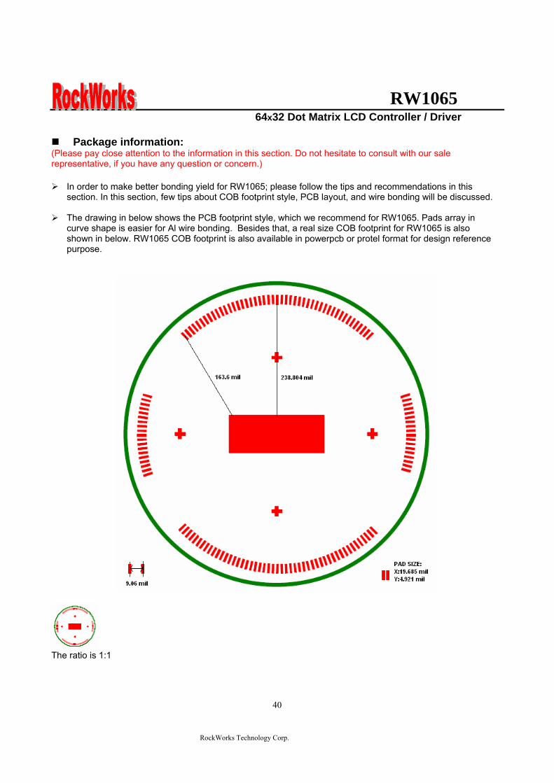
RW1065 64x32 Dot Matrix LCD Controller Driver
RockWorks Technology Corp
40
Package information (Please pay close attention to the information in this section Do not hesitate to consult with our sale representative if you have any question or concern)
In order to make better bonding yield for RW1065 please follow the tips and recommendations in this section In this section few tips about COB footprint style PCB layout and wire bonding will be discussed
The drawing in below shows the PCB footprint style which we recommend for RW1065 Pads array in
curve shape is easier for Al wire bonding Besides that a real size COB footprint for RW1065 is also shown in below RW1065 COB footprint is also available in powerpcb or protel format for design reference purpose
The ratio is 11
RW1065 64x32 Dot Matrix LCD Controller Driver
RockWorks Technology Corp
41
During COB footprint design there have some tips about footprint that the PCB designer should know The angle between bonding wire and vertical line should less than 45 Otherwise the wire shorts would become very easy to happen at fours corners of the chip
The angle between bonding wire and vertical line could be reduced by expanding the distance between pads array and the chip In addition reducing length in horizon direction of pads array could minimize the angle between bonding wire and vertical line The picture in below will help to illustrate this concept From the experiences COB footprint style affects the bonding yield
Bad Wires are too close to each other
The angle between bonding wire and vertical line is greater than 45
The angle between bonding wire and vertical line is less than 45
Wires are not too close to each other
Reducing length in horizon direction of pads array could minimize the angle between bonding wire and vertical line
The angle between bonding wire and vertical line could be reduced by expanding the distance between pads array and the chip
RW1065 64x32 Dot Matrix LCD Controller Driver
RockWorks Technology Corp
42
If the gap between pads of COB footprint is filled with solder mask coating it is difficult to bond Al wire to
the pads The top solder masks layer that overlap COB footprint area should be removed
Please use 1 mils diameter Al wire for RW1065 wire bonding
1 2 3 4 5 6
A
B
C
D
654321
D
C
B
A
Title
Number RevisionSize
C
Date 29-Aug-2007 Sheet of File D公司資料99seMyDesignddb Drawn By
RW1065
COM131
COM142
COM153
COM164
COM175
COM186
COM197
COM208
COM219
COM2210
COM2311
COM2412
COM2513
COM2614
COM2715
COM2816
COM2917
COM3018
COM3119
SEG
6320
SEG
6221
SEG
6122
SEG
6023
SEG
5924
SEG
5825
SEG
5726
SEG
5627
SEG
5528
SEG
5429
SEG
5330
SEG
5231
SEG
5132
SEG
5033
SEG
4934
SEG
4835
SEG
4736
SEG
4637
SEG
4538
SEG
4439
SEG
4340
SEG
4241
SEG
4142
SEG
4043
SEG
3944
SEG
3845
SEG
3746
SEG
3647
SEG
3548
SEG
3449
SEG
3350
SEG
3251
SEG
3152
SEG
3053
SEG
2954
SEG
2855
SEG
2756
SEG
2657
SEG
2558
SEG
2459
SEG
2360
SEG
2261
SEG
2162
SEG
2063
SEG
1964
SEG
1865
SEG
1766
SEG
1667
SEG
1568
SEG
1469
SEG13 70SEG12 71SEG11 72SEG10 73SEG9 74SEG8 75SEG7 76SEG6 77SEG5 78SEG4 79SEG3 80SEG2 81SEG1 82SEG0 83ADCP 84CLL 85
VSS
86D
087
D1
88D
289
D3
90D
491
D5
92D
693
D7
94C
S1B
P95
CS2
P96
ERD
P97
AO
P(R
S)98
RW
RP
99V
DD
100
RST
P10
1C
LSP
102
FRR
103
MSP
104
BS1
P10
5B
S0P
106
SHLP
107
VD
D2
108
CA
P2N
109
CA
P2P
110
CA
P1P
111
CA
P1N
112
CA
P3P
113
VO
UT
114
V0
115
VR
AB
116
V3
117
V2
118
V4
119
V1
120
CO
M0
121
CO
M1
122
CO
M2
123
CO
M3
124
CO
M4
125
CO
M5
126
CO
M6
127
CO
M7
128
CO
M8
129
CO
M9
130
CO
M10
131
CO
M11
132
CO
M12
133
4897x1902 um
IC1
RW1065
C9CAPR4
100R0603
R30R0603
C8
CAP
C7
CAP
R2
100R0603
R1
0R0603C6 22uf
R50R
R6300R
R7RES1
R8NC R9
100R0603
VDD
R10
NC
R11
100R0603
R12
100R0603
R13
NC
R14
100R0603
R15
NC
VDD
D0
D1
D2
D3
D4
D5
D6
D7
DB[07]
VDDC5
01uf0603
VD
D
CS2
P
123456789
1011121314151617181920
J1
CON20
C1201uf0603
R3951K0603
VDD
CAP Value1UF~22UF
2XPut C6C8 Short R1R3Open R2R4C7C93XPut C6C8C9 R4Short R1Open R2R3C74XOpen R1R3
BS0 BS1 Bias0 0
0 1
1 0
11
15 bias
16 bias
18 bias
19 bias
ADC=0 SEG0lt~column address 00Hnormal(default) ADC=1 SEG0lt~column address 3FHinverted
SHL=0 Normal COM0~gtCOM63(default)SHL=1 Reverse direction COM63~gtCOM0
R16100R0603
LCD PANEL 64X32RockWorks
RW1065 64X32
COM0-31 SEG0-63SHL=0 ADC=0
SHL=1COM31-0
ADC=1SEG63-0
if use single chip for 32 command displaythe display command must select 164 dutyDisplay panel must select 164 duty type
VO
UT
C3P
C1N
C1P
C2P
C2N
VDD2
ADC
SHL
BS0
BS1
CLLADC
V1
V2
V3
V4
VR
AB
V0
VO
UT
C3P
C1N
C1P
C2P
C2N
VD
D2
SHL
BS0
BS1
FRR
RST
P
RW
RS
E CS1
B
CS1
V0RSRWED0D1D2D3D4D5D6D7
RSTPAK
C4
22uf
RBRES1
RA1RES1
C2
22uf
C1
22uf
C3
22uf
C0
22uf
R20
100k0603
R21
100k0603
R17
200K0603
V1
V2
V3
V4 VRAB
V0
V0
OPTION
B
R18
300R0603
RA2RES1
VADJ
R19100R
R23 RES1R22 0R
R24
RES1
R25
0R
VDD
CS1BP
CS2P
CS1
CS1
R26
22R0603
R27
22R0603
C1047uf
C11
01uf
VSS_INVDD_IN
D1DIODE
FGND
鐵框地
VSS
VDD
R28 10RR29 10RR30 10RR31 10RR32 10RR33 10RR34 10RR35 10RR36 10RR37 10RR38 10R
VADJ
1 2 3 4 5 6
A
B
C
D
654321
D
C
B
A
Title
Number RevisionSize
C
Date 29-Aug-2007 Sheet of File D公司資料99seMyDesignddb Drawn By
RW1065
COM131
COM142
COM153
COM164
COM175
COM186
COM197
COM208
COM219
COM2210
COM2311
COM2412
COM2513
COM2614
COM2715
COM2816
COM2917
COM3018
COM3119
SEG
6320
SEG
6221
SEG
6122
SEG
6023
SEG
5924
SEG
5825
SEG
5726
SEG
5627
SEG
5528
SEG
5429
SEG
5330
SEG
5231
SEG
5132
SEG
5033
SEG
4934
SEG
4835
SEG
4736
SEG
4637
SEG
4538
SEG
4439
SEG
4340
SEG
4241
SEG
4142
SEG
4043
SEG
3944
SEG
3845
SEG
3746
SEG
3647
SEG
3548
SEG
3449
SEG
3350
SEG
3251
SEG
3152
SEG
3053
SEG
2954
SEG
2855
SEG
2756
SEG
2657
SEG
2558
SEG
2459
SEG
2360
SEG
2261
SEG
2162
SEG
2063
SEG
1964
SEG
1865
SEG
1766
SEG
1667
SEG
1568
SEG
1469
SEG13 70SEG12 71SEG11 72SEG10 73SEG9 74SEG8 75SEG7 76SEG6 77SEG5 78SEG4 79SEG3 80SEG2 81SEG1 82SEG0 83ADCP 84CLL 85
VSS
86D
087
D1
88D
289
D3
90D
491
D5
92D
693
D7
94C
S1B
P95
CS2
P96
ERD
P97
AO
P(R
S)98
RW
RP
99V
DD
100
RST
P10
1C
LSP
102
FRR
103
MSP
104
BS1
P10
5B
S0P
106
SHLP
107
VD
D2
108
CA
P2N
109
CA
P2P
110
CA
P1P
111
CA
P1N
112
CA
P3P
113
VO
UT
114
V0
115
VR
AB
116
V3
117
V2
118
V4
119
V1
120
CO
M0
121
CO
M1
122
CO
M2
123
CO
M3
124
CO
M4
125
CO
M5
126
CO
M6
127
CO
M7
128
CO
M8
129
CO
M9
130
CO
M10
131
CO
M11
132
CO
M12
133
4897x1902 um
IC1
RW1065 Master
RW1065
COM131
COM142
COM153
COM164
COM175
COM186
COM197
COM208
COM219
COM2210
COM2311
COM2412
COM2513
COM2614
COM2715
COM2816
COM2917
COM3018
COM3119
SEG
6320
SEG
6221
SEG
6122
SEG
6023
SEG
5924
SEG
5825
SEG
5726
SEG
5627
SEG
5528
SEG
5429
SEG
5330
SEG
5231
SEG
5132
SEG
5033
SEG
4934
SEG
4835
SEG
4736
SEG
4637
SEG
4538
SEG
4439
SEG
4340
SEG
4241
SEG
4142
SEG
4043
SEG
3944
SEG
3845
SEG
3746
SEG
3647
SEG
3548
SEG
3449
SEG
3350
SEG
3251
SEG
3152
SEG
3053
SEG
2954
SEG
2855
SEG
2756
SEG
2657
SEG
2558
SEG
2459
SEG
2360
SEG
2261
SEG
2162
SEG
2063
SEG
1964
SEG
1865
SEG
1766
SEG
1667
SEG
1568
SEG
1469
SEG13 70SEG12 71SEG11 72SEG10 73SEG9 74SEG8 75SEG7 76SEG6 77SEG5 78SEG4 79SEG3 80SEG2 81SEG1 82SEG0 83ADCP 84CLL 85
VSS
86D
087
D1
88D
289
D3
90D
491
D5
92D
693
D7
94C
S1B
P95
CS2
P96
ERD
P97
AO
P(R
S)98
RW
RP
99V
DD
100
RST
P10
1C
LSP
102
FRR
103
MSP
104
BS1
P10
5B
S0P
106
SHLP
107
VD
D2
108
CA
P2N
109
CA
P2P
110
CA
P1P
111
CA
P1N
112
CA
P3P
113
VO
UT
114
V0
115
VR
AB
116
V3
117
V2
118
V4
119
V1
120
CO
M0
121
CO
M1
122
CO
M2
123
CO
M3
124
CO
M4
125
CO
M5
126
CO
M6
127
CO
M7
128
CO
M8
129
CO
M9
130
CO
M10
131
CO
M11
132
CO
M12
133
4897x1902 um
IC2
RW1065 Slave
C4
22uf
RBRES1
RA1RES1
C2
22uf
C1
22uf
C3
22uf
C0
22ufC9CAPR4
100R0603
R30R0603
C8
CAP
C7
CAP
R2
100R0603
R1
0R0603C6 22uf
R50R0603
R6300R0603
R7RES1
R8NC R9
100R0603
VDD
R10
NC
R11
100R0603
R12
NC
R13
100R0603
R14
100R0603
R15
NC
R16
100R0603
R17
NC
VDD
D0
D1
D2
D3
D4
D5
D6
D7
D0
D1
D2
D3
D4
D5
D6
D7
DB[07] DB[07]
VDDC10
01uf0603
VD
D
IC1_
CS2
P
VDD
IC2_
CS2
P
VD
D
C11
01uf0603
VSS
VSS
LCD PANEL 128X64
Master COM0-31 Slave COM32-63
Master SEG0-63 Slave SEG64-127
123456789
1011121314151617181920
J1
CON20
Master Slave
CAP Value1UF~22UF
2XPut C6C8 Short R1R3Open R2R4C7C93XPut C6C8C9 R4Short R1Open R2R3C74XOpen R1R3
RockWorksRW1065 128x64
BS0 BS1 Bias0 0
0 1
1 0
11
15 bias
16 bias
18 bias
19 bias
ADC=0 SEG0lt~column address 00Hnormal(default) ADC=1 SEG0lt~column address 3FHinverted
SHL=0 Normal COM0~gtCOM63(default)SHL=1 Reverse direction COM63~gtCOM0Both Master and Slave should set identical SHL value
SHL=0 SHL=0
ADC=0 ADC=0
Slave COM31-0
Slave SEG127-64
SHL=1
ADC=1
SHL=1Master COM63-32
ADC=1Master SEG63-0
R18100R0603
R22
100k0603
R23
100k0603
C501uF0603
R4551K0603
VDD
R19
200K0603
ADC1
ADC2
SHL
BS0
BS1
VDD2
V1
V2
V3
V4 VRAB
V0
V0V
OU
T
C3P
C1N
C1P
C2P
C2N
V1
V2
V3
V4
VR
AB
V0
VO
UT
C3P
C1N
C1P
C2P
C2N
VD
D2
SHL
BS0
BS1
FRR
RST
P
RW
RS
E IC1_
CS1
BP
V1
V2
V3
V4
VR
AB
V0
VO
UT
VD
D2
SHL
BS0
BS1
FRR
RST
P
RW
RS
E IC2_
CS1
BP
CLLADC1
CLLADC2
RSTP
CS1CS2
V0RSRWED0D1D2D3D4D5D6D7
AK
OPTION
R20
300R0603
RA2RES1
VADJ
R21
100R
B
R25 RESR24 0R
R26 RES R27 0RVDD
IC1_CS1BP
IC1_CS2P
CS1
CS1
R28 0R R29 RES
R30 RES R31 0R
IC2_CS1BP
IC2_CS2P
CS2
CS2
R32
22R0603
R33
22R0603
C1001uf
C11
47uf
D1DIODE
FGND
鐵框地
VSS
VDD
R34 10RR35 10RR36 10RR37 10RR38 10RR39 10RR40 10RR41 10RR42 10RR43 10RR44 10R
VSS_INVDD_IN
VADJ
VDD
1 2 3 4 5 6 7 8
A
B
C
D
87654321
D
C
B
A
Title
Number RevisionSize
D
Date 29-Aug-2007 Sheet of File D公司資料 99seMyDesignddb Drawn By
C422uf
RBRES1
RA1RES1
C3
22uf
C2
22uf
C1
22uf
C0
22ufC9CAPR4
100R0603
R30R0603
C8
CAP
C7
CAP
R2
100R0603
R1
0R0603C6 22uf
R220R0603
R23300R0603
R24RES1
R39
NCR40
100 ohm0603
VDD
R41
NC
R42
100 ohm0603
R43
NC
R44
100 ohm0603
R45
NC
R46
100 ohm0603
R47
100 ohm0603
R48
NC
R49
100 ohm0603
R50
NC
VDDCAP Value1UF~22UF
2XPut C6C8 Short R1R3Open R2R4C7C93XPut C6C8C9 R4Short R1Open R2R3C74XOpen R1R3
BS0 BS1 Bias0 0
0 1
1 0
11
15 bias
16 bias
18 bias
19 bias
ADC=0 SEG0lt~column address 00Hnormal(default)
ADC=1 SEG0lt~column address 3FHinverted
SHL=0 Normal COM0~gtCOM63(default)SHL=1 Reverse direction COM63~gtCOM0Both Master and Slave should set identical SHL value
R7
100k0603
R8
100k0603
V1
V2
V3
V4
V0
VRAB
V0
R5
200K
VDD2
VO
UT
C3P
C1N
C1P
C2P
C2N
ADC1
ADC2
ADC3
SHL
BS0
BS1
CS1CS2CS3
V0RSRWED0D1D2D3D4D5D6D7
RSTP
R3851K0603
C5
01uF
VDD
OPTION
R6
300R0603R9100R
RA2RES1
VADJ
RW1065
COM131
COM142
COM153
COM164
COM175
COM186
COM197
COM208
COM219
COM2210
COM2311
COM2412
COM2513
COM2614
COM2715
COM2816
COM2917
COM3018
COM3119
SEG
6320
SEG
6221
SEG
6122
SEG
6023
SEG
5924
SEG
5825
SEG
5726
SEG
5627
SEG
5528
SEG
5429
SEG
5330
SEG
5231
SEG
5132
SEG
5033
SEG
4934
SEG
4835
SEG
4736
SEG
4637
SEG
4538
SEG
4439
SEG
4340
SEG
4241
SEG
4142
SEG
4043
SEG
3944
SEG
3845
SEG
3746
SEG
3647
SEG
3548
SEG
3449
SEG
3350
SEG
3251
SEG
3152
SEG
3053
SEG
2954
SEG
2855
SEG
2756
SEG
2657
SEG
2558
SEG
2459
SEG
2360
SEG
2261
SEG
2162
SEG
2063
SEG
1964
SEG
1865
SEG
1766
SEG
1667
SEG
1568
SEG
1469
SEG13 70SEG12 71SEG11 72SEG10 73SEG9 74SEG8 75SEG7 76SEG6 77SEG5 78SEG4 79SEG3 80SEG2 81SEG1 82SEG0 83ADCP 84CLL 85
VSS
86D
087
D1
88D
289
D3
90D
491
D5
92D
693
D7
94C
S1B
P95
CS2
P96
ERD
P97
AO
P(R
S)98
RW
RP
99V
DD
100
RST
P10
1C
LSP
102
FRR
103
MSP
104
BS1
P10
5B
S0P
106
SHLP
107
VD
D2
108
CA
P2N
109
CA
P2P
110
CA
P1P
111
CA
P1N
112
CA
P3P
113
VO
UT
114
V0
115
VR
AB
116
V3
117
V2
118
V4
119
V1
120
CO
M0
121
CO
M1
122
CO
M2
123
CO
M3
124
CO
M4
125
CO
M5
126
CO
M6
127
CO
M7
128
CO
M8
129
CO
M9
130
CO
M10
131
CO
M11
132
CO
M12
133
4897x1902 um
IC1
RW1065 Master
RW1065
COM131
COM142
COM153
COM164
COM175
COM186
COM197
COM208
COM219
COM2210
COM2311
COM2412
COM2513
COM2614
COM2715
COM2816
COM2917
COM3018
COM3119
SEG
6320
SEG
6221
SEG
6122
SEG
6023
SEG
5924
SEG
5825
SEG
5726
SEG
5627
SEG
5528
SEG
5429
SEG
5330
SEG
5231
SEG
5132
SEG
5033
SEG
4934
SEG
4835
SEG
4736
SEG
4637
SEG
4538
SEG
4439
SEG
4340
SEG
4241
SEG
4142
SEG
4043
SEG
3944
SEG
3845
SEG
3746
SEG
3647
SEG
3548
SEG
3449
SEG
3350
SEG
3251
SEG
3152
SEG
3053
SEG
2954
SEG
2855
SEG
2756
SEG
2657
SEG
2558
SEG
2459
SEG
2360
SEG
2261
SEG
2162
SEG
2063
SEG
1964
SEG
1865
SEG
1766
SEG
1667
SEG
1568
SEG
1469
SEG13 70SEG12 71SEG11 72SEG10 73SEG9 74SEG8 75SEG7 76SEG6 77SEG5 78SEG4 79SEG3 80SEG2 81SEG1 82SEG0 83ADCP 84CLL 85
VSS
86D
087
D1
88D
289
D3
90D
491
D5
92D
693
D7
94C
S1B
P95
CS2
P96
ERD
P97
AO
P(R
S)98
RW
RP
99V
DD
100
RST
P10
1C
LSP
102
FRR
103
MSP
104
BS1
P10
5B
S0P
106
SHLP
107
VD
D2
108
CA
P2N
109
CA
P2P
110
CA
P1P
111
CA
P1N
112
CA
P3P
113
VO
UT
114
V0
115
VR
AB
116
V3
117
V2
118
V4
119
V1
120
CO
M0
121
CO
M1
122
CO
M2
123
CO
M3
124
CO
M4
125
CO
M5
126
CO
M6
127
CO
M7
128
CO
M8
129
CO
M9
130
CO
M10
131
CO
M11
132
CO
M12
133
4897x1902 um
IC2
RW1065 Slave
D0
D1
D2
D3
D4
D5
D6
D7
D0
D1
D2
D3
D4
D5
D6
D7
DB[07] DB[07]
VDDC8
01uf0603
VD
D
VDD
VD
D
C9
01uf0603
VSS
VSS
LCD PANEL 192X64
Master COM0-31 Slave COM32-63
Master SEG0-63 Slave SEG64-127
Master Slave
RockWorksRW1065 192x64
RW1065
COM131
COM142
COM153
COM164
COM175
COM186
COM197
COM208
COM219
COM2210
COM2311
COM2412
COM2513
COM2614
COM2715
COM2816
COM2917
COM3018
COM3119
SEG
6320
SEG
6221
SEG
6122
SEG
6023
SEG
5924
SEG
5825
SEG
5726
SEG
5627
SEG
5528
SEG
5429
SEG
5330
SEG
5231
SEG
5132
SEG
5033
SEG
4934
SEG
4835
SEG
4736
SEG
4637
SEG
4538
SEG
4439
SEG
4340
SEG
4241
SEG
4142
SEG
4043
SEG
3944
SEG
3845
SEG
3746
SEG
3647
SEG
3548
SEG
3449
SEG
3350
SEG
3251
SEG
3152
SEG
3053
SEG
2954
SEG
2855
SEG
2756
SEG
2657
SEG
2558
SEG
2459
SEG
2360
SEG
2261
SEG
2162
SEG
2063
SEG
1964
SEG
1865
SEG
1766
SEG
1667
SEG
1568
SEG
1469
SEG13 70SEG12 71SEG11 72SEG10 73SEG9 74SEG8 75SEG7 76SEG6 77SEG5 78SEG4 79SEG3 80SEG2 81SEG1 82SEG0 83ADCP 84CLL 85
VSS
86D
087
D1
88D
289
D3
90D
491
D5
92D
693
D7
94C
S1B
P95
CS2
P96
ERD
P97
AO
P(R
S)98
RW
RP
99V
DD
100
RST
P10
1C
LSP
102
FRR
103
MSP
104
BS1
P10
5B
S0P
106
SHLP
107
VD
D2
108
CA
P2N
109
CA
P2P
110
CA
P1P
111
CA
P1N
112
CA
P3P
113
VO
UT
114
V0
115
VR
AB
116
V3
117
V2
118
V4
119
V1
120
CO
M0
121
CO
M1
122
CO
M2
123
CO
M3
124
CO
M4
125
CO
M5
126
CO
M6
127
CO
M7
128
CO
M8
129
CO
M9
130
CO
M10
131
CO
M11
132
CO
M12
133
4897x1902 um
IC3
RW1065 Slave
D0
D1
D2
D3
D4
D5
D6
D7
DB[07]
VSS
VSS
VDD
VD
D
C10
01uf0603
Slave SEG128-192
Slave
SHL=0 SHL=0
Master COM63-32SHL=1 SHL=1
Slave COM31-0ADC=0 ADC=0 ADC=0
ADC=1 ADC=1 ADC=1Master SEG63-0 Slave SEG127-64 Slave SEG192-128
R50100R0603
V1
V2
V3
V4
VR
AB
V0
VO
UT
C3P
C1N
C1P
C2P
C2N
VD
D2
SHL
BS0
BS1
FRR
RST
P
RW
RS
E V1
V2
V3
V4
VR
AB
V0
VO
UT
VD
D2
SHL
BS0
BS1
FRR
RST
P
RW
RS
E V1
V2
V3
V4
VR
AB
V0
VO
UT
VD
D2
SHL
BS0
BS1
FRR
RST
P
RW
RS
E
CLL CLL CLLADC1 ADC2 ADC3
R25 10RR26 10RR27 10RR28 10RR29 10RR30 10RR31 10RR32 10RR33 10RR34 10RR35 10R
R36
22R0603
D1DIODE
R3722R0603
C647uf
C701uf
VSS_INVDD_IN
VSS
VDD
VADJ
123456789
101112131415161718192021222324
J1
CON24
AK
FGND
鐵框地
IC1_
CS1
BP
IC1_
CS2
P
IC2_
CS2
PIC
2_C
S1B
P
IC3_
CS1
BP
IC3_
CS2
B
R10 0R R11 RES
R12 RES R13 0RVDD
IC1_CS2B
IC1_CS1BPCS1
CS1
R14 0R R15 RES
R16 RES R17 0RVDDIC2_CS2B
IC2_CS1BPCS2
CS2
R18 0R R19 RES
R20 RES R21 0RVDDIC3_CS2B
IC3_CS1BPCS3
CS3
B
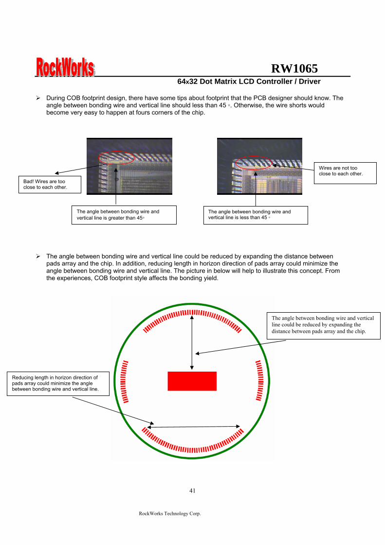
RW1065 64x32 Dot Matrix LCD Controller Driver
RockWorks Technology Corp
41
During COB footprint design there have some tips about footprint that the PCB designer should know The angle between bonding wire and vertical line should less than 45 Otherwise the wire shorts would become very easy to happen at fours corners of the chip
The angle between bonding wire and vertical line could be reduced by expanding the distance between pads array and the chip In addition reducing length in horizon direction of pads array could minimize the angle between bonding wire and vertical line The picture in below will help to illustrate this concept From the experiences COB footprint style affects the bonding yield
Bad Wires are too close to each other
The angle between bonding wire and vertical line is greater than 45
The angle between bonding wire and vertical line is less than 45
Wires are not too close to each other
Reducing length in horizon direction of pads array could minimize the angle between bonding wire and vertical line
The angle between bonding wire and vertical line could be reduced by expanding the distance between pads array and the chip
RW1065 64x32 Dot Matrix LCD Controller Driver
RockWorks Technology Corp
42
If the gap between pads of COB footprint is filled with solder mask coating it is difficult to bond Al wire to
the pads The top solder masks layer that overlap COB footprint area should be removed
Please use 1 mils diameter Al wire for RW1065 wire bonding
1 2 3 4 5 6
A
B
C
D
654321
D
C
B
A
Title
Number RevisionSize
C
Date 29-Aug-2007 Sheet of File D公司資料99seMyDesignddb Drawn By
RW1065
COM131
COM142
COM153
COM164
COM175
COM186
COM197
COM208
COM219
COM2210
COM2311
COM2412
COM2513
COM2614
COM2715
COM2816
COM2917
COM3018
COM3119
SEG
6320
SEG
6221
SEG
6122
SEG
6023
SEG
5924
SEG
5825
SEG
5726
SEG
5627
SEG
5528
SEG
5429
SEG
5330
SEG
5231
SEG
5132
SEG
5033
SEG
4934
SEG
4835
SEG
4736
SEG
4637
SEG
4538
SEG
4439
SEG
4340
SEG
4241
SEG
4142
SEG
4043
SEG
3944
SEG
3845
SEG
3746
SEG
3647
SEG
3548
SEG
3449
SEG
3350
SEG
3251
SEG
3152
SEG
3053
SEG
2954
SEG
2855
SEG
2756
SEG
2657
SEG
2558
SEG
2459
SEG
2360
SEG
2261
SEG
2162
SEG
2063
SEG
1964
SEG
1865
SEG
1766
SEG
1667
SEG
1568
SEG
1469
SEG13 70SEG12 71SEG11 72SEG10 73SEG9 74SEG8 75SEG7 76SEG6 77SEG5 78SEG4 79SEG3 80SEG2 81SEG1 82SEG0 83ADCP 84CLL 85
VSS
86D
087
D1
88D
289
D3
90D
491
D5
92D
693
D7
94C
S1B
P95
CS2
P96
ERD
P97
AO
P(R
S)98
RW
RP
99V
DD
100
RST
P10
1C
LSP
102
FRR
103
MSP
104
BS1
P10
5B
S0P
106
SHLP
107
VD
D2
108
CA
P2N
109
CA
P2P
110
CA
P1P
111
CA
P1N
112
CA
P3P
113
VO
UT
114
V0
115
VR
AB
116
V3
117
V2
118
V4
119
V1
120
CO
M0
121
CO
M1
122
CO
M2
123
CO
M3
124
CO
M4
125
CO
M5
126
CO
M6
127
CO
M7
128
CO
M8
129
CO
M9
130
CO
M10
131
CO
M11
132
CO
M12
133
4897x1902 um
IC1
RW1065
C9CAPR4
100R0603
R30R0603
C8
CAP
C7
CAP
R2
100R0603
R1
0R0603C6 22uf
R50R
R6300R
R7RES1
R8NC R9
100R0603
VDD
R10
NC
R11
100R0603
R12
100R0603
R13
NC
R14
100R0603
R15
NC
VDD
D0
D1
D2
D3
D4
D5
D6
D7
DB[07]
VDDC5
01uf0603
VD
D
CS2
P
123456789
1011121314151617181920
J1
CON20
C1201uf0603
R3951K0603
VDD
CAP Value1UF~22UF
2XPut C6C8 Short R1R3Open R2R4C7C93XPut C6C8C9 R4Short R1Open R2R3C74XOpen R1R3
BS0 BS1 Bias0 0
0 1
1 0
11
15 bias
16 bias
18 bias
19 bias
ADC=0 SEG0lt~column address 00Hnormal(default) ADC=1 SEG0lt~column address 3FHinverted
SHL=0 Normal COM0~gtCOM63(default)SHL=1 Reverse direction COM63~gtCOM0
R16100R0603
LCD PANEL 64X32RockWorks
RW1065 64X32
COM0-31 SEG0-63SHL=0 ADC=0
SHL=1COM31-0
ADC=1SEG63-0
if use single chip for 32 command displaythe display command must select 164 dutyDisplay panel must select 164 duty type
VO
UT
C3P
C1N
C1P
C2P
C2N
VDD2
ADC
SHL
BS0
BS1
CLLADC
V1
V2
V3
V4
VR
AB
V0
VO
UT
C3P
C1N
C1P
C2P
C2N
VD
D2
SHL
BS0
BS1
FRR
RST
P
RW
RS
E CS1
B
CS1
V0RSRWED0D1D2D3D4D5D6D7
RSTPAK
C4
22uf
RBRES1
RA1RES1
C2
22uf
C1
22uf
C3
22uf
C0
22uf
R20
100k0603
R21
100k0603
R17
200K0603
V1
V2
V3
V4 VRAB
V0
V0
OPTION
B
R18
300R0603
RA2RES1
VADJ
R19100R
R23 RES1R22 0R
R24
RES1
R25
0R
VDD
CS1BP
CS2P
CS1
CS1
R26
22R0603
R27
22R0603
C1047uf
C11
01uf
VSS_INVDD_IN
D1DIODE
FGND
鐵框地
VSS
VDD
R28 10RR29 10RR30 10RR31 10RR32 10RR33 10RR34 10RR35 10RR36 10RR37 10RR38 10R
VADJ
1 2 3 4 5 6
A
B
C
D
654321
D
C
B
A
Title
Number RevisionSize
C
Date 29-Aug-2007 Sheet of File D公司資料99seMyDesignddb Drawn By
RW1065
COM131
COM142
COM153
COM164
COM175
COM186
COM197
COM208
COM219
COM2210
COM2311
COM2412
COM2513
COM2614
COM2715
COM2816
COM2917
COM3018
COM3119
SEG
6320
SEG
6221
SEG
6122
SEG
6023
SEG
5924
SEG
5825
SEG
5726
SEG
5627
SEG
5528
SEG
5429
SEG
5330
SEG
5231
SEG
5132
SEG
5033
SEG
4934
SEG
4835
SEG
4736
SEG
4637
SEG
4538
SEG
4439
SEG
4340
SEG
4241
SEG
4142
SEG
4043
SEG
3944
SEG
3845
SEG
3746
SEG
3647
SEG
3548
SEG
3449
SEG
3350
SEG
3251
SEG
3152
SEG
3053
SEG
2954
SEG
2855
SEG
2756
SEG
2657
SEG
2558
SEG
2459
SEG
2360
SEG
2261
SEG
2162
SEG
2063
SEG
1964
SEG
1865
SEG
1766
SEG
1667
SEG
1568
SEG
1469
SEG13 70SEG12 71SEG11 72SEG10 73SEG9 74SEG8 75SEG7 76SEG6 77SEG5 78SEG4 79SEG3 80SEG2 81SEG1 82SEG0 83ADCP 84CLL 85
VSS
86D
087
D1
88D
289
D3
90D
491
D5
92D
693
D7
94C
S1B
P95
CS2
P96
ERD
P97
AO
P(R
S)98
RW
RP
99V
DD
100
RST
P10
1C
LSP
102
FRR
103
MSP
104
BS1
P10
5B
S0P
106
SHLP
107
VD
D2
108
CA
P2N
109
CA
P2P
110
CA
P1P
111
CA
P1N
112
CA
P3P
113
VO
UT
114
V0
115
VR
AB
116
V3
117
V2
118
V4
119
V1
120
CO
M0
121
CO
M1
122
CO
M2
123
CO
M3
124
CO
M4
125
CO
M5
126
CO
M6
127
CO
M7
128
CO
M8
129
CO
M9
130
CO
M10
131
CO
M11
132
CO
M12
133
4897x1902 um
IC1
RW1065 Master
RW1065
COM131
COM142
COM153
COM164
COM175
COM186
COM197
COM208
COM219
COM2210
COM2311
COM2412
COM2513
COM2614
COM2715
COM2816
COM2917
COM3018
COM3119
SEG
6320
SEG
6221
SEG
6122
SEG
6023
SEG
5924
SEG
5825
SEG
5726
SEG
5627
SEG
5528
SEG
5429
SEG
5330
SEG
5231
SEG
5132
SEG
5033
SEG
4934
SEG
4835
SEG
4736
SEG
4637
SEG
4538
SEG
4439
SEG
4340
SEG
4241
SEG
4142
SEG
4043
SEG
3944
SEG
3845
SEG
3746
SEG
3647
SEG
3548
SEG
3449
SEG
3350
SEG
3251
SEG
3152
SEG
3053
SEG
2954
SEG
2855
SEG
2756
SEG
2657
SEG
2558
SEG
2459
SEG
2360
SEG
2261
SEG
2162
SEG
2063
SEG
1964
SEG
1865
SEG
1766
SEG
1667
SEG
1568
SEG
1469
SEG13 70SEG12 71SEG11 72SEG10 73SEG9 74SEG8 75SEG7 76SEG6 77SEG5 78SEG4 79SEG3 80SEG2 81SEG1 82SEG0 83ADCP 84CLL 85
VSS
86D
087
D1
88D
289
D3
90D
491
D5
92D
693
D7
94C
S1B
P95
CS2
P96
ERD
P97
AO
P(R
S)98
RW
RP
99V
DD
100
RST
P10
1C
LSP
102
FRR
103
MSP
104
BS1
P10
5B
S0P
106
SHLP
107
VD
D2
108
CA
P2N
109
CA
P2P
110
CA
P1P
111
CA
P1N
112
CA
P3P
113
VO
UT
114
V0
115
VR
AB
116
V3
117
V2
118
V4
119
V1
120
CO
M0
121
CO
M1
122
CO
M2
123
CO
M3
124
CO
M4
125
CO
M5
126
CO
M6
127
CO
M7
128
CO
M8
129
CO
M9
130
CO
M10
131
CO
M11
132
CO
M12
133
4897x1902 um
IC2
RW1065 Slave
C4
22uf
RBRES1
RA1RES1
C2
22uf
C1
22uf
C3
22uf
C0
22ufC9CAPR4
100R0603
R30R0603
C8
CAP
C7
CAP
R2
100R0603
R1
0R0603C6 22uf
R50R0603
R6300R0603
R7RES1
R8NC R9
100R0603
VDD
R10
NC
R11
100R0603
R12
NC
R13
100R0603
R14
100R0603
R15
NC
R16
100R0603
R17
NC
VDD
D0
D1
D2
D3
D4
D5
D6
D7
D0
D1
D2
D3
D4
D5
D6
D7
DB[07] DB[07]
VDDC10
01uf0603
VD
D
IC1_
CS2
P
VDD
IC2_
CS2
P
VD
D
C11
01uf0603
VSS
VSS
LCD PANEL 128X64
Master COM0-31 Slave COM32-63
Master SEG0-63 Slave SEG64-127
123456789
1011121314151617181920
J1
CON20
Master Slave
CAP Value1UF~22UF
2XPut C6C8 Short R1R3Open R2R4C7C93XPut C6C8C9 R4Short R1Open R2R3C74XOpen R1R3
RockWorksRW1065 128x64
BS0 BS1 Bias0 0
0 1
1 0
11
15 bias
16 bias
18 bias
19 bias
ADC=0 SEG0lt~column address 00Hnormal(default) ADC=1 SEG0lt~column address 3FHinverted
SHL=0 Normal COM0~gtCOM63(default)SHL=1 Reverse direction COM63~gtCOM0Both Master and Slave should set identical SHL value
SHL=0 SHL=0
ADC=0 ADC=0
Slave COM31-0
Slave SEG127-64
SHL=1
ADC=1
SHL=1Master COM63-32
ADC=1Master SEG63-0
R18100R0603
R22
100k0603
R23
100k0603
C501uF0603
R4551K0603
VDD
R19
200K0603
ADC1
ADC2
SHL
BS0
BS1
VDD2
V1
V2
V3
V4 VRAB
V0
V0V
OU
T
C3P
C1N
C1P
C2P
C2N
V1
V2
V3
V4
VR
AB
V0
VO
UT
C3P
C1N
C1P
C2P
C2N
VD
D2
SHL
BS0
BS1
FRR
RST
P
RW
RS
E IC1_
CS1
BP
V1
V2
V3
V4
VR
AB
V0
VO
UT
VD
D2
SHL
BS0
BS1
FRR
RST
P
RW
RS
E IC2_
CS1
BP
CLLADC1
CLLADC2
RSTP
CS1CS2
V0RSRWED0D1D2D3D4D5D6D7
AK
OPTION
R20
300R0603
RA2RES1
VADJ
R21
100R
B
R25 RESR24 0R
R26 RES R27 0RVDD
IC1_CS1BP
IC1_CS2P
CS1
CS1
R28 0R R29 RES
R30 RES R31 0R
IC2_CS1BP
IC2_CS2P
CS2
CS2
R32
22R0603
R33
22R0603
C1001uf
C11
47uf
D1DIODE
FGND
鐵框地
VSS
VDD
R34 10RR35 10RR36 10RR37 10RR38 10RR39 10RR40 10RR41 10RR42 10RR43 10RR44 10R
VSS_INVDD_IN
VADJ
VDD
1 2 3 4 5 6 7 8
A
B
C
D
87654321
D
C
B
A
Title
Number RevisionSize
D
Date 29-Aug-2007 Sheet of File D公司資料 99seMyDesignddb Drawn By
C422uf
RBRES1
RA1RES1
C3
22uf
C2
22uf
C1
22uf
C0
22ufC9CAPR4
100R0603
R30R0603
C8
CAP
C7
CAP
R2
100R0603
R1
0R0603C6 22uf
R220R0603
R23300R0603
R24RES1
R39
NCR40
100 ohm0603
VDD
R41
NC
R42
100 ohm0603
R43
NC
R44
100 ohm0603
R45
NC
R46
100 ohm0603
R47
100 ohm0603
R48
NC
R49
100 ohm0603
R50
NC
VDDCAP Value1UF~22UF
2XPut C6C8 Short R1R3Open R2R4C7C93XPut C6C8C9 R4Short R1Open R2R3C74XOpen R1R3
BS0 BS1 Bias0 0
0 1
1 0
11
15 bias
16 bias
18 bias
19 bias
ADC=0 SEG0lt~column address 00Hnormal(default)
ADC=1 SEG0lt~column address 3FHinverted
SHL=0 Normal COM0~gtCOM63(default)SHL=1 Reverse direction COM63~gtCOM0Both Master and Slave should set identical SHL value
R7
100k0603
R8
100k0603
V1
V2
V3
V4
V0
VRAB
V0
R5
200K
VDD2
VO
UT
C3P
C1N
C1P
C2P
C2N
ADC1
ADC2
ADC3
SHL
BS0
BS1
CS1CS2CS3
V0RSRWED0D1D2D3D4D5D6D7
RSTP
R3851K0603
C5
01uF
VDD
OPTION
R6
300R0603R9100R
RA2RES1
VADJ
RW1065
COM131
COM142
COM153
COM164
COM175
COM186
COM197
COM208
COM219
COM2210
COM2311
COM2412
COM2513
COM2614
COM2715
COM2816
COM2917
COM3018
COM3119
SEG
6320
SEG
6221
SEG
6122
SEG
6023
SEG
5924
SEG
5825
SEG
5726
SEG
5627
SEG
5528
SEG
5429
SEG
5330
SEG
5231
SEG
5132
SEG
5033
SEG
4934
SEG
4835
SEG
4736
SEG
4637
SEG
4538
SEG
4439
SEG
4340
SEG
4241
SEG
4142
SEG
4043
SEG
3944
SEG
3845
SEG
3746
SEG
3647
SEG
3548
SEG
3449
SEG
3350
SEG
3251
SEG
3152
SEG
3053
SEG
2954
SEG
2855
SEG
2756
SEG
2657
SEG
2558
SEG
2459
SEG
2360
SEG
2261
SEG
2162
SEG
2063
SEG
1964
SEG
1865
SEG
1766
SEG
1667
SEG
1568
SEG
1469
SEG13 70SEG12 71SEG11 72SEG10 73SEG9 74SEG8 75SEG7 76SEG6 77SEG5 78SEG4 79SEG3 80SEG2 81SEG1 82SEG0 83ADCP 84CLL 85
VSS
86D
087
D1
88D
289
D3
90D
491
D5
92D
693
D7
94C
S1B
P95
CS2
P96
ERD
P97
AO
P(R
S)98
RW
RP
99V
DD
100
RST
P10
1C
LSP
102
FRR
103
MSP
104
BS1
P10
5B
S0P
106
SHLP
107
VD
D2
108
CA
P2N
109
CA
P2P
110
CA
P1P
111
CA
P1N
112
CA
P3P
113
VO
UT
114
V0
115
VR
AB
116
V3
117
V2
118
V4
119
V1
120
CO
M0
121
CO
M1
122
CO
M2
123
CO
M3
124
CO
M4
125
CO
M5
126
CO
M6
127
CO
M7
128
CO
M8
129
CO
M9
130
CO
M10
131
CO
M11
132
CO
M12
133
4897x1902 um
IC1
RW1065 Master
RW1065
COM131
COM142
COM153
COM164
COM175
COM186
COM197
COM208
COM219
COM2210
COM2311
COM2412
COM2513
COM2614
COM2715
COM2816
COM2917
COM3018
COM3119
SEG
6320
SEG
6221
SEG
6122
SEG
6023
SEG
5924
SEG
5825
SEG
5726
SEG
5627
SEG
5528
SEG
5429
SEG
5330
SEG
5231
SEG
5132
SEG
5033
SEG
4934
SEG
4835
SEG
4736
SEG
4637
SEG
4538
SEG
4439
SEG
4340
SEG
4241
SEG
4142
SEG
4043
SEG
3944
SEG
3845
SEG
3746
SEG
3647
SEG
3548
SEG
3449
SEG
3350
SEG
3251
SEG
3152
SEG
3053
SEG
2954
SEG
2855
SEG
2756
SEG
2657
SEG
2558
SEG
2459
SEG
2360
SEG
2261
SEG
2162
SEG
2063
SEG
1964
SEG
1865
SEG
1766
SEG
1667
SEG
1568
SEG
1469
SEG13 70SEG12 71SEG11 72SEG10 73SEG9 74SEG8 75SEG7 76SEG6 77SEG5 78SEG4 79SEG3 80SEG2 81SEG1 82SEG0 83ADCP 84CLL 85
VSS
86D
087
D1
88D
289
D3
90D
491
D5
92D
693
D7
94C
S1B
P95
CS2
P96
ERD
P97
AO
P(R
S)98
RW
RP
99V
DD
100
RST
P10
1C
LSP
102
FRR
103
MSP
104
BS1
P10
5B
S0P
106
SHLP
107
VD
D2
108
CA
P2N
109
CA
P2P
110
CA
P1P
111
CA
P1N
112
CA
P3P
113
VO
UT
114
V0
115
VR
AB
116
V3
117
V2
118
V4
119
V1
120
CO
M0
121
CO
M1
122
CO
M2
123
CO
M3
124
CO
M4
125
CO
M5
126
CO
M6
127
CO
M7
128
CO
M8
129
CO
M9
130
CO
M10
131
CO
M11
132
CO
M12
133
4897x1902 um
IC2
RW1065 Slave
D0
D1
D2
D3
D4
D5
D6
D7
D0
D1
D2
D3
D4
D5
D6
D7
DB[07] DB[07]
VDDC8
01uf0603
VD
D
VDD
VD
D
C9
01uf0603
VSS
VSS
LCD PANEL 192X64
Master COM0-31 Slave COM32-63
Master SEG0-63 Slave SEG64-127
Master Slave
RockWorksRW1065 192x64
RW1065
COM131
COM142
COM153
COM164
COM175
COM186
COM197
COM208
COM219
COM2210
COM2311
COM2412
COM2513
COM2614
COM2715
COM2816
COM2917
COM3018
COM3119
SEG
6320
SEG
6221
SEG
6122
SEG
6023
SEG
5924
SEG
5825
SEG
5726
SEG
5627
SEG
5528
SEG
5429
SEG
5330
SEG
5231
SEG
5132
SEG
5033
SEG
4934
SEG
4835
SEG
4736
SEG
4637
SEG
4538
SEG
4439
SEG
4340
SEG
4241
SEG
4142
SEG
4043
SEG
3944
SEG
3845
SEG
3746
SEG
3647
SEG
3548
SEG
3449
SEG
3350
SEG
3251
SEG
3152
SEG
3053
SEG
2954
SEG
2855
SEG
2756
SEG
2657
SEG
2558
SEG
2459
SEG
2360
SEG
2261
SEG
2162
SEG
2063
SEG
1964
SEG
1865
SEG
1766
SEG
1667
SEG
1568
SEG
1469
SEG13 70SEG12 71SEG11 72SEG10 73SEG9 74SEG8 75SEG7 76SEG6 77SEG5 78SEG4 79SEG3 80SEG2 81SEG1 82SEG0 83ADCP 84CLL 85
VSS
86D
087
D1
88D
289
D3
90D
491
D5
92D
693
D7
94C
S1B
P95
CS2
P96
ERD
P97
AO
P(R
S)98
RW
RP
99V
DD
100
RST
P10
1C
LSP
102
FRR
103
MSP
104
BS1
P10
5B
S0P
106
SHLP
107
VD
D2
108
CA
P2N
109
CA
P2P
110
CA
P1P
111
CA
P1N
112
CA
P3P
113
VO
UT
114
V0
115
VR
AB
116
V3
117
V2
118
V4
119
V1
120
CO
M0
121
CO
M1
122
CO
M2
123
CO
M3
124
CO
M4
125
CO
M5
126
CO
M6
127
CO
M7
128
CO
M8
129
CO
M9
130
CO
M10
131
CO
M11
132
CO
M12
133
4897x1902 um
IC3
RW1065 Slave
D0
D1
D2
D3
D4
D5
D6
D7
DB[07]
VSS
VSS
VDD
VD
D
C10
01uf0603
Slave SEG128-192
Slave
SHL=0 SHL=0
Master COM63-32SHL=1 SHL=1
Slave COM31-0ADC=0 ADC=0 ADC=0
ADC=1 ADC=1 ADC=1Master SEG63-0 Slave SEG127-64 Slave SEG192-128
R50100R0603
V1
V2
V3
V4
VR
AB
V0
VO
UT
C3P
C1N
C1P
C2P
C2N
VD
D2
SHL
BS0
BS1
FRR
RST
P
RW
RS
E V1
V2
V3
V4
VR
AB
V0
VO
UT
VD
D2
SHL
BS0
BS1
FRR
RST
P
RW
RS
E V1
V2
V3
V4
VR
AB
V0
VO
UT
VD
D2
SHL
BS0
BS1
FRR
RST
P
RW
RS
E
CLL CLL CLLADC1 ADC2 ADC3
R25 10RR26 10RR27 10RR28 10RR29 10RR30 10RR31 10RR32 10RR33 10RR34 10RR35 10R
R36
22R0603
D1DIODE
R3722R0603
C647uf
C701uf
VSS_INVDD_IN
VSS
VDD
VADJ
123456789
101112131415161718192021222324
J1
CON24
AK
FGND
鐵框地
IC1_
CS1
BP
IC1_
CS2
P
IC2_
CS2
PIC
2_C
S1B
P
IC3_
CS1
BP
IC3_
CS2
B
R10 0R R11 RES
R12 RES R13 0RVDD
IC1_CS2B
IC1_CS1BPCS1
CS1
R14 0R R15 RES
R16 RES R17 0RVDDIC2_CS2B
IC2_CS1BPCS2
CS2
R18 0R R19 RES
R20 RES R21 0RVDDIC3_CS2B
IC3_CS1BPCS3
CS3
B
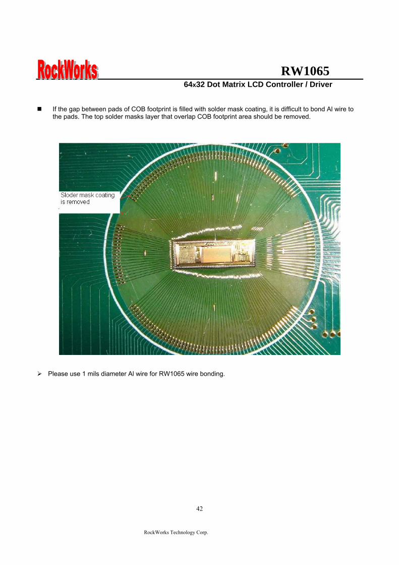
RW1065 64x32 Dot Matrix LCD Controller Driver
RockWorks Technology Corp
42
If the gap between pads of COB footprint is filled with solder mask coating it is difficult to bond Al wire to
the pads The top solder masks layer that overlap COB footprint area should be removed
Please use 1 mils diameter Al wire for RW1065 wire bonding
1 2 3 4 5 6
A
B
C
D
654321
D
C
B
A
Title
Number RevisionSize
C
Date 29-Aug-2007 Sheet of File D公司資料99seMyDesignddb Drawn By
RW1065
COM131
COM142
COM153
COM164
COM175
COM186
COM197
COM208
COM219
COM2210
COM2311
COM2412
COM2513
COM2614
COM2715
COM2816
COM2917
COM3018
COM3119
SEG
6320
SEG
6221
SEG
6122
SEG
6023
SEG
5924
SEG
5825
SEG
5726
SEG
5627
SEG
5528
SEG
5429
SEG
5330
SEG
5231
SEG
5132
SEG
5033
SEG
4934
SEG
4835
SEG
4736
SEG
4637
SEG
4538
SEG
4439
SEG
4340
SEG
4241
SEG
4142
SEG
4043
SEG
3944
SEG
3845
SEG
3746
SEG
3647
SEG
3548
SEG
3449
SEG
3350
SEG
3251
SEG
3152
SEG
3053
SEG
2954
SEG
2855
SEG
2756
SEG
2657
SEG
2558
SEG
2459
SEG
2360
SEG
2261
SEG
2162
SEG
2063
SEG
1964
SEG
1865
SEG
1766
SEG
1667
SEG
1568
SEG
1469
SEG13 70SEG12 71SEG11 72SEG10 73SEG9 74SEG8 75SEG7 76SEG6 77SEG5 78SEG4 79SEG3 80SEG2 81SEG1 82SEG0 83ADCP 84CLL 85
VSS
86D
087
D1
88D
289
D3
90D
491
D5
92D
693
D7
94C
S1B
P95
CS2
P96
ERD
P97
AO
P(R
S)98
RW
RP
99V
DD
100
RST
P10
1C
LSP
102
FRR
103
MSP
104
BS1
P10
5B
S0P
106
SHLP
107
VD
D2
108
CA
P2N
109
CA
P2P
110
CA
P1P
111
CA
P1N
112
CA
P3P
113
VO
UT
114
V0
115
VR
AB
116
V3
117
V2
118
V4
119
V1
120
CO
M0
121
CO
M1
122
CO
M2
123
CO
M3
124
CO
M4
125
CO
M5
126
CO
M6
127
CO
M7
128
CO
M8
129
CO
M9
130
CO
M10
131
CO
M11
132
CO
M12
133
4897x1902 um
IC1
RW1065
C9CAPR4
100R0603
R30R0603
C8
CAP
C7
CAP
R2
100R0603
R1
0R0603C6 22uf
R50R
R6300R
R7RES1
R8NC R9
100R0603
VDD
R10
NC
R11
100R0603
R12
100R0603
R13
NC
R14
100R0603
R15
NC
VDD
D0
D1
D2
D3
D4
D5
D6
D7
DB[07]
VDDC5
01uf0603
VD
D
CS2
P
123456789
1011121314151617181920
J1
CON20
C1201uf0603
R3951K0603
VDD
CAP Value1UF~22UF
2XPut C6C8 Short R1R3Open R2R4C7C93XPut C6C8C9 R4Short R1Open R2R3C74XOpen R1R3
BS0 BS1 Bias0 0
0 1
1 0
11
15 bias
16 bias
18 bias
19 bias
ADC=0 SEG0lt~column address 00Hnormal(default) ADC=1 SEG0lt~column address 3FHinverted
SHL=0 Normal COM0~gtCOM63(default)SHL=1 Reverse direction COM63~gtCOM0
R16100R0603
LCD PANEL 64X32RockWorks
RW1065 64X32
COM0-31 SEG0-63SHL=0 ADC=0
SHL=1COM31-0
ADC=1SEG63-0
if use single chip for 32 command displaythe display command must select 164 dutyDisplay panel must select 164 duty type
VO
UT
C3P
C1N
C1P
C2P
C2N
VDD2
ADC
SHL
BS0
BS1
CLLADC
V1
V2
V3
V4
VR
AB
V0
VO
UT
C3P
C1N
C1P
C2P
C2N
VD
D2
SHL
BS0
BS1
FRR
RST
P
RW
RS
E CS1
B
CS1
V0RSRWED0D1D2D3D4D5D6D7
RSTPAK
C4
22uf
RBRES1
RA1RES1
C2
22uf
C1
22uf
C3
22uf
C0
22uf
R20
100k0603
R21
100k0603
R17
200K0603
V1
V2
V3
V4 VRAB
V0
V0
OPTION
B
R18
300R0603
RA2RES1
VADJ
R19100R
R23 RES1R22 0R
R24
RES1
R25
0R
VDD
CS1BP
CS2P
CS1
CS1
R26
22R0603
R27
22R0603
C1047uf
C11
01uf
VSS_INVDD_IN
D1DIODE
FGND
鐵框地
VSS
VDD
R28 10RR29 10RR30 10RR31 10RR32 10RR33 10RR34 10RR35 10RR36 10RR37 10RR38 10R
VADJ
1 2 3 4 5 6
A
B
C
D
654321
D
C
B
A
Title
Number RevisionSize
C
Date 29-Aug-2007 Sheet of File D公司資料99seMyDesignddb Drawn By
RW1065
COM131
COM142
COM153
COM164
COM175
COM186
COM197
COM208
COM219
COM2210
COM2311
COM2412
COM2513
COM2614
COM2715
COM2816
COM2917
COM3018
COM3119
SEG
6320
SEG
6221
SEG
6122
SEG
6023
SEG
5924
SEG
5825
SEG
5726
SEG
5627
SEG
5528
SEG
5429
SEG
5330
SEG
5231
SEG
5132
SEG
5033
SEG
4934
SEG
4835
SEG
4736
SEG
4637
SEG
4538
SEG
4439
SEG
4340
SEG
4241
SEG
4142
SEG
4043
SEG
3944
SEG
3845
SEG
3746
SEG
3647
SEG
3548
SEG
3449
SEG
3350
SEG
3251
SEG
3152
SEG
3053
SEG
2954
SEG
2855
SEG
2756
SEG
2657
SEG
2558
SEG
2459
SEG
2360
SEG
2261
SEG
2162
SEG
2063
SEG
1964
SEG
1865
SEG
1766
SEG
1667
SEG
1568
SEG
1469
SEG13 70SEG12 71SEG11 72SEG10 73SEG9 74SEG8 75SEG7 76SEG6 77SEG5 78SEG4 79SEG3 80SEG2 81SEG1 82SEG0 83ADCP 84CLL 85
VSS
86D
087
D1
88D
289
D3
90D
491
D5
92D
693
D7
94C
S1B
P95
CS2
P96
ERD
P97
AO
P(R
S)98
RW
RP
99V
DD
100
RST
P10
1C
LSP
102
FRR
103
MSP
104
BS1
P10
5B
S0P
106
SHLP
107
VD
D2
108
CA
P2N
109
CA
P2P
110
CA
P1P
111
CA
P1N
112
CA
P3P
113
VO
UT
114
V0
115
VR
AB
116
V3
117
V2
118
V4
119
V1
120
CO
M0
121
CO
M1
122
CO
M2
123
CO
M3
124
CO
M4
125
CO
M5
126
CO
M6
127
CO
M7
128
CO
M8
129
CO
M9
130
CO
M10
131
CO
M11
132
CO
M12
133
4897x1902 um
IC1
RW1065 Master
RW1065
COM131
COM142
COM153
COM164
COM175
COM186
COM197
COM208
COM219
COM2210
COM2311
COM2412
COM2513
COM2614
COM2715
COM2816
COM2917
COM3018
COM3119
SEG
6320
SEG
6221
SEG
6122
SEG
6023
SEG
5924
SEG
5825
SEG
5726
SEG
5627
SEG
5528
SEG
5429
SEG
5330
SEG
5231
SEG
5132
SEG
5033
SEG
4934
SEG
4835
SEG
4736
SEG
4637
SEG
4538
SEG
4439
SEG
4340
SEG
4241
SEG
4142
SEG
4043
SEG
3944
SEG
3845
SEG
3746
SEG
3647
SEG
3548
SEG
3449
SEG
3350
SEG
3251
SEG
3152
SEG
3053
SEG
2954
SEG
2855
SEG
2756
SEG
2657
SEG
2558
SEG
2459
SEG
2360
SEG
2261
SEG
2162
SEG
2063
SEG
1964
SEG
1865
SEG
1766
SEG
1667
SEG
1568
SEG
1469
SEG13 70SEG12 71SEG11 72SEG10 73SEG9 74SEG8 75SEG7 76SEG6 77SEG5 78SEG4 79SEG3 80SEG2 81SEG1 82SEG0 83ADCP 84CLL 85
VSS
86D
087
D1
88D
289
D3
90D
491
D5
92D
693
D7
94C
S1B
P95
CS2
P96
ERD
P97
AO
P(R
S)98
RW
RP
99V
DD
100
RST
P10
1C
LSP
102
FRR
103
MSP
104
BS1
P10
5B
S0P
106
SHLP
107
VD
D2
108
CA
P2N
109
CA
P2P
110
CA
P1P
111
CA
P1N
112
CA
P3P
113
VO
UT
114
V0
115
VR
AB
116
V3
117
V2
118
V4
119
V1
120
CO
M0
121
CO
M1
122
CO
M2
123
CO
M3
124
CO
M4
125
CO
M5
126
CO
M6
127
CO
M7
128
CO
M8
129
CO
M9
130
CO
M10
131
CO
M11
132
CO
M12
133
4897x1902 um
IC2
RW1065 Slave
C4
22uf
RBRES1
RA1RES1
C2
22uf
C1
22uf
C3
22uf
C0
22ufC9CAPR4
100R0603
R30R0603
C8
CAP
C7
CAP
R2
100R0603
R1
0R0603C6 22uf
R50R0603
R6300R0603
R7RES1
R8NC R9
100R0603
VDD
R10
NC
R11
100R0603
R12
NC
R13
100R0603
R14
100R0603
R15
NC
R16
100R0603
R17
NC
VDD
D0
D1
D2
D3
D4
D5
D6
D7
D0
D1
D2
D3
D4
D5
D6
D7
DB[07] DB[07]
VDDC10
01uf0603
VD
D
IC1_
CS2
P
VDD
IC2_
CS2
P
VD
D
C11
01uf0603
VSS
VSS
LCD PANEL 128X64
Master COM0-31 Slave COM32-63
Master SEG0-63 Slave SEG64-127
123456789
1011121314151617181920
J1
CON20
Master Slave
CAP Value1UF~22UF
2XPut C6C8 Short R1R3Open R2R4C7C93XPut C6C8C9 R4Short R1Open R2R3C74XOpen R1R3
RockWorksRW1065 128x64
BS0 BS1 Bias0 0
0 1
1 0
11
15 bias
16 bias
18 bias
19 bias
ADC=0 SEG0lt~column address 00Hnormal(default) ADC=1 SEG0lt~column address 3FHinverted
SHL=0 Normal COM0~gtCOM63(default)SHL=1 Reverse direction COM63~gtCOM0Both Master and Slave should set identical SHL value
SHL=0 SHL=0
ADC=0 ADC=0
Slave COM31-0
Slave SEG127-64
SHL=1
ADC=1
SHL=1Master COM63-32
ADC=1Master SEG63-0
R18100R0603
R22
100k0603
R23
100k0603
C501uF0603
R4551K0603
VDD
R19
200K0603
ADC1
ADC2
SHL
BS0
BS1
VDD2
V1
V2
V3
V4 VRAB
V0
V0V
OU
T
C3P
C1N
C1P
C2P
C2N
V1
V2
V3
V4
VR
AB
V0
VO
UT
C3P
C1N
C1P
C2P
C2N
VD
D2
SHL
BS0
BS1
FRR
RST
P
RW
RS
E IC1_
CS1
BP
V1
V2
V3
V4
VR
AB
V0
VO
UT
VD
D2
SHL
BS0
BS1
FRR
RST
P
RW
RS
E IC2_
CS1
BP
CLLADC1
CLLADC2
RSTP
CS1CS2
V0RSRWED0D1D2D3D4D5D6D7
AK
OPTION
R20
300R0603
RA2RES1
VADJ
R21
100R
B
R25 RESR24 0R
R26 RES R27 0RVDD
IC1_CS1BP
IC1_CS2P
CS1
CS1
R28 0R R29 RES
R30 RES R31 0R
IC2_CS1BP
IC2_CS2P
CS2
CS2
R32
22R0603
R33
22R0603
C1001uf
C11
47uf
D1DIODE
FGND
鐵框地
VSS
VDD
R34 10RR35 10RR36 10RR37 10RR38 10RR39 10RR40 10RR41 10RR42 10RR43 10RR44 10R
VSS_INVDD_IN
VADJ
VDD
1 2 3 4 5 6 7 8
A
B
C
D
87654321
D
C
B
A
Title
Number RevisionSize
D
Date 29-Aug-2007 Sheet of File D公司資料 99seMyDesignddb Drawn By
C422uf
RBRES1
RA1RES1
C3
22uf
C2
22uf
C1
22uf
C0
22ufC9CAPR4
100R0603
R30R0603
C8
CAP
C7
CAP
R2
100R0603
R1
0R0603C6 22uf
R220R0603
R23300R0603
R24RES1
R39
NCR40
100 ohm0603
VDD
R41
NC
R42
100 ohm0603
R43
NC
R44
100 ohm0603
R45
NC
R46
100 ohm0603
R47
100 ohm0603
R48
NC
R49
100 ohm0603
R50
NC
VDDCAP Value1UF~22UF
2XPut C6C8 Short R1R3Open R2R4C7C93XPut C6C8C9 R4Short R1Open R2R3C74XOpen R1R3
BS0 BS1 Bias0 0
0 1
1 0
11
15 bias
16 bias
18 bias
19 bias
ADC=0 SEG0lt~column address 00Hnormal(default)
ADC=1 SEG0lt~column address 3FHinverted
SHL=0 Normal COM0~gtCOM63(default)SHL=1 Reverse direction COM63~gtCOM0Both Master and Slave should set identical SHL value
R7
100k0603
R8
100k0603
V1
V2
V3
V4
V0
VRAB
V0
R5
200K
VDD2
VO
UT
C3P
C1N
C1P
C2P
C2N
ADC1
ADC2
ADC3
SHL
BS0
BS1
CS1CS2CS3
V0RSRWED0D1D2D3D4D5D6D7
RSTP
R3851K0603
C5
01uF
VDD
OPTION
R6
300R0603R9100R
RA2RES1
VADJ
RW1065
COM131
COM142
COM153
COM164
COM175
COM186
COM197
COM208
COM219
COM2210
COM2311
COM2412
COM2513
COM2614
COM2715
COM2816
COM2917
COM3018
COM3119
SEG
6320
SEG
6221
SEG
6122
SEG
6023
SEG
5924
SEG
5825
SEG
5726
SEG
5627
SEG
5528
SEG
5429
SEG
5330
SEG
5231
SEG
5132
SEG
5033
SEG
4934
SEG
4835
SEG
4736
SEG
4637
SEG
4538
SEG
4439
SEG
4340
SEG
4241
SEG
4142
SEG
4043
SEG
3944
SEG
3845
SEG
3746
SEG
3647
SEG
3548
SEG
3449
SEG
3350
SEG
3251
SEG
3152
SEG
3053
SEG
2954
SEG
2855
SEG
2756
SEG
2657
SEG
2558
SEG
2459
SEG
2360
SEG
2261
SEG
2162
SEG
2063
SEG
1964
SEG
1865
SEG
1766
SEG
1667
SEG
1568
SEG
1469
SEG13 70SEG12 71SEG11 72SEG10 73SEG9 74SEG8 75SEG7 76SEG6 77SEG5 78SEG4 79SEG3 80SEG2 81SEG1 82SEG0 83ADCP 84CLL 85
VSS
86D
087
D1
88D
289
D3
90D
491
D5
92D
693
D7
94C
S1B
P95
CS2
P96
ERD
P97
AO
P(R
S)98
RW
RP
99V
DD
100
RST
P10
1C
LSP
102
FRR
103
MSP
104
BS1
P10
5B
S0P
106
SHLP
107
VD
D2
108
CA
P2N
109
CA
P2P
110
CA
P1P
111
CA
P1N
112
CA
P3P
113
VO
UT
114
V0
115
VR
AB
116
V3
117
V2
118
V4
119
V1
120
CO
M0
121
CO
M1
122
CO
M2
123
CO
M3
124
CO
M4
125
CO
M5
126
CO
M6
127
CO
M7
128
CO
M8
129
CO
M9
130
CO
M10
131
CO
M11
132
CO
M12
133
4897x1902 um
IC1
RW1065 Master
RW1065
COM131
COM142
COM153
COM164
COM175
COM186
COM197
COM208
COM219
COM2210
COM2311
COM2412
COM2513
COM2614
COM2715
COM2816
COM2917
COM3018
COM3119
SEG
6320
SEG
6221
SEG
6122
SEG
6023
SEG
5924
SEG
5825
SEG
5726
SEG
5627
SEG
5528
SEG
5429
SEG
5330
SEG
5231
SEG
5132
SEG
5033
SEG
4934
SEG
4835
SEG
4736
SEG
4637
SEG
4538
SEG
4439
SEG
4340
SEG
4241
SEG
4142
SEG
4043
SEG
3944
SEG
3845
SEG
3746
SEG
3647
SEG
3548
SEG
3449
SEG
3350
SEG
3251
SEG
3152
SEG
3053
SEG
2954
SEG
2855
SEG
2756
SEG
2657
SEG
2558
SEG
2459
SEG
2360
SEG
2261
SEG
2162
SEG
2063
SEG
1964
SEG
1865
SEG
1766
SEG
1667
SEG
1568
SEG
1469
SEG13 70SEG12 71SEG11 72SEG10 73SEG9 74SEG8 75SEG7 76SEG6 77SEG5 78SEG4 79SEG3 80SEG2 81SEG1 82SEG0 83ADCP 84CLL 85
VSS
86D
087
D1
88D
289
D3
90D
491
D5
92D
693
D7
94C
S1B
P95
CS2
P96
ERD
P97
AO
P(R
S)98
RW
RP
99V
DD
100
RST
P10
1C
LSP
102
FRR
103
MSP
104
BS1
P10
5B
S0P
106
SHLP
107
VD
D2
108
CA
P2N
109
CA
P2P
110
CA
P1P
111
CA
P1N
112
CA
P3P
113
VO
UT
114
V0
115
VR
AB
116
V3
117
V2
118
V4
119
V1
120
CO
M0
121
CO
M1
122
CO
M2
123
CO
M3
124
CO
M4
125
CO
M5
126
CO
M6
127
CO
M7
128
CO
M8
129
CO
M9
130
CO
M10
131
CO
M11
132
CO
M12
133
4897x1902 um
IC2
RW1065 Slave
D0
D1
D2
D3
D4
D5
D6
D7
D0
D1
D2
D3
D4
D5
D6
D7
DB[07] DB[07]
VDDC8
01uf0603
VD
D
VDD
VD
D
C9
01uf0603
VSS
VSS
LCD PANEL 192X64
Master COM0-31 Slave COM32-63
Master SEG0-63 Slave SEG64-127
Master Slave
RockWorksRW1065 192x64
RW1065
COM131
COM142
COM153
COM164
COM175
COM186
COM197
COM208
COM219
COM2210
COM2311
COM2412
COM2513
COM2614
COM2715
COM2816
COM2917
COM3018
COM3119
SEG
6320
SEG
6221
SEG
6122
SEG
6023
SEG
5924
SEG
5825
SEG
5726
SEG
5627
SEG
5528
SEG
5429
SEG
5330
SEG
5231
SEG
5132
SEG
5033
SEG
4934
SEG
4835
SEG
4736
SEG
4637
SEG
4538
SEG
4439
SEG
4340
SEG
4241
SEG
4142
SEG
4043
SEG
3944
SEG
3845
SEG
3746
SEG
3647
SEG
3548
SEG
3449
SEG
3350
SEG
3251
SEG
3152
SEG
3053
SEG
2954
SEG
2855
SEG
2756
SEG
2657
SEG
2558
SEG
2459
SEG
2360
SEG
2261
SEG
2162
SEG
2063
SEG
1964
SEG
1865
SEG
1766
SEG
1667
SEG
1568
SEG
1469
SEG13 70SEG12 71SEG11 72SEG10 73SEG9 74SEG8 75SEG7 76SEG6 77SEG5 78SEG4 79SEG3 80SEG2 81SEG1 82SEG0 83ADCP 84CLL 85
VSS
86D
087
D1
88D
289
D3
90D
491
D5
92D
693
D7
94C
S1B
P95
CS2
P96
ERD
P97
AO
P(R
S)98
RW
RP
99V
DD
100
RST
P10
1C
LSP
102
FRR
103
MSP
104
BS1
P10
5B
S0P
106
SHLP
107
VD
D2
108
CA
P2N
109
CA
P2P
110
CA
P1P
111
CA
P1N
112
CA
P3P
113
VO
UT
114
V0
115
VR
AB
116
V3
117
V2
118
V4
119
V1
120
CO
M0
121
CO
M1
122
CO
M2
123
CO
M3
124
CO
M4
125
CO
M5
126
CO
M6
127
CO
M7
128
CO
M8
129
CO
M9
130
CO
M10
131
CO
M11
132
CO
M12
133
4897x1902 um
IC3
RW1065 Slave
D0
D1
D2
D3
D4
D5
D6
D7
DB[07]
VSS
VSS
VDD
VD
D
C10
01uf0603
Slave SEG128-192
Slave
SHL=0 SHL=0
Master COM63-32SHL=1 SHL=1
Slave COM31-0ADC=0 ADC=0 ADC=0
ADC=1 ADC=1 ADC=1Master SEG63-0 Slave SEG127-64 Slave SEG192-128
R50100R0603
V1
V2
V3
V4
VR
AB
V0
VO
UT
C3P
C1N
C1P
C2P
C2N
VD
D2
SHL
BS0
BS1
FRR
RST
P
RW
RS
E V1
V2
V3
V4
VR
AB
V0
VO
UT
VD
D2
SHL
BS0
BS1
FRR
RST
P
RW
RS
E V1
V2
V3
V4
VR
AB
V0
VO
UT
VD
D2
SHL
BS0
BS1
FRR
RST
P
RW
RS
E
CLL CLL CLLADC1 ADC2 ADC3
R25 10RR26 10RR27 10RR28 10RR29 10RR30 10RR31 10RR32 10RR33 10RR34 10RR35 10R
R36
22R0603
D1DIODE
R3722R0603
C647uf
C701uf
VSS_INVDD_IN
VSS
VDD
VADJ
123456789
101112131415161718192021222324
J1
CON24
AK
FGND
鐵框地
IC1_
CS1
BP
IC1_
CS2
P
IC2_
CS2
PIC
2_C
S1B
P
IC3_
CS1
BP
IC3_
CS2
B
R10 0R R11 RES
R12 RES R13 0RVDD
IC1_CS2B
IC1_CS1BPCS1
CS1
R14 0R R15 RES
R16 RES R17 0RVDDIC2_CS2B
IC2_CS1BPCS2
CS2
R18 0R R19 RES
R20 RES R21 0RVDDIC3_CS2B
IC3_CS1BPCS3
CS3
B
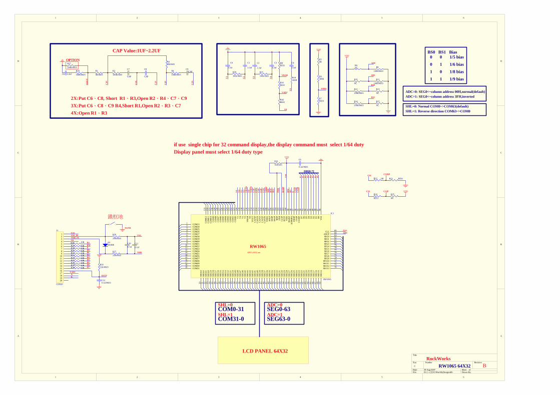
1 2 3 4 5 6
A
B
C
D
654321
D
C
B
A
Title
Number RevisionSize
C
Date 29-Aug-2007 Sheet of File D公司資料99seMyDesignddb Drawn By
RW1065
COM131
COM142
COM153
COM164
COM175
COM186
COM197
COM208
COM219
COM2210
COM2311
COM2412
COM2513
COM2614
COM2715
COM2816
COM2917
COM3018
COM3119
SEG
6320
SEG
6221
SEG
6122
SEG
6023
SEG
5924
SEG
5825
SEG
5726
SEG
5627
SEG
5528
SEG
5429
SEG
5330
SEG
5231
SEG
5132
SEG
5033
SEG
4934
SEG
4835
SEG
4736
SEG
4637
SEG
4538
SEG
4439
SEG
4340
SEG
4241
SEG
4142
SEG
4043
SEG
3944
SEG
3845
SEG
3746
SEG
3647
SEG
3548
SEG
3449
SEG
3350
SEG
3251
SEG
3152
SEG
3053
SEG
2954
SEG
2855
SEG
2756
SEG
2657
SEG
2558
SEG
2459
SEG
2360
SEG
2261
SEG
2162
SEG
2063
SEG
1964
SEG
1865
SEG
1766
SEG
1667
SEG
1568
SEG
1469
SEG13 70SEG12 71SEG11 72SEG10 73SEG9 74SEG8 75SEG7 76SEG6 77SEG5 78SEG4 79SEG3 80SEG2 81SEG1 82SEG0 83ADCP 84CLL 85
VSS
86D
087
D1
88D
289
D3
90D
491
D5
92D
693
D7
94C
S1B
P95
CS2
P96
ERD
P97
AO
P(R
S)98
RW
RP
99V
DD
100
RST
P10
1C
LSP
102
FRR
103
MSP
104
BS1
P10
5B
S0P
106
SHLP
107
VD
D2
108
CA
P2N
109
CA
P2P
110
CA
P1P
111
CA
P1N
112
CA
P3P
113
VO
UT
114
V0
115
VR
AB
116
V3
117
V2
118
V4
119
V1
120
CO
M0
121
CO
M1
122
CO
M2
123
CO
M3
124
CO
M4
125
CO
M5
126
CO
M6
127
CO
M7
128
CO
M8
129
CO
M9
130
CO
M10
131
CO
M11
132
CO
M12
133
4897x1902 um
IC1
RW1065
C9CAPR4
100R0603
R30R0603
C8
CAP
C7
CAP
R2
100R0603
R1
0R0603C6 22uf
R50R
R6300R
R7RES1
R8NC R9
100R0603
VDD
R10
NC
R11
100R0603
R12
100R0603
R13
NC
R14
100R0603
R15
NC
VDD
D0
D1
D2
D3
D4
D5
D6
D7
DB[07]
VDDC5
01uf0603
VD
D
CS2
P
123456789
1011121314151617181920
J1
CON20
C1201uf0603
R3951K0603
VDD
CAP Value1UF~22UF
2XPut C6C8 Short R1R3Open R2R4C7C93XPut C6C8C9 R4Short R1Open R2R3C74XOpen R1R3
BS0 BS1 Bias0 0
0 1
1 0
11
15 bias
16 bias
18 bias
19 bias
ADC=0 SEG0lt~column address 00Hnormal(default) ADC=1 SEG0lt~column address 3FHinverted
SHL=0 Normal COM0~gtCOM63(default)SHL=1 Reverse direction COM63~gtCOM0
R16100R0603
LCD PANEL 64X32RockWorks
RW1065 64X32
COM0-31 SEG0-63SHL=0 ADC=0
SHL=1COM31-0
ADC=1SEG63-0
if use single chip for 32 command displaythe display command must select 164 dutyDisplay panel must select 164 duty type
VO
UT
C3P
C1N
C1P
C2P
C2N
VDD2
ADC
SHL
BS0
BS1
CLLADC
V1
V2
V3
V4
VR
AB
V0
VO
UT
C3P
C1N
C1P
C2P
C2N
VD
D2
SHL
BS0
BS1
FRR
RST
P
RW
RS
E CS1
B
CS1
V0RSRWED0D1D2D3D4D5D6D7
RSTPAK
C4
22uf
RBRES1
RA1RES1
C2
22uf
C1
22uf
C3
22uf
C0
22uf
R20
100k0603
R21
100k0603
R17
200K0603
V1
V2
V3
V4 VRAB
V0
V0
OPTION
B
R18
300R0603
RA2RES1
VADJ
R19100R
R23 RES1R22 0R
R24
RES1
R25
0R
VDD
CS1BP
CS2P
CS1
CS1
R26
22R0603
R27
22R0603
C1047uf
C11
01uf
VSS_INVDD_IN
D1DIODE
FGND
鐵框地
VSS
VDD
R28 10RR29 10RR30 10RR31 10RR32 10RR33 10RR34 10RR35 10RR36 10RR37 10RR38 10R
VADJ
1 2 3 4 5 6
A
B
C
D
654321
D
C
B
A
Title
Number RevisionSize
C
Date 29-Aug-2007 Sheet of File D公司資料99seMyDesignddb Drawn By
RW1065
COM131
COM142
COM153
COM164
COM175
COM186
COM197
COM208
COM219
COM2210
COM2311
COM2412
COM2513
COM2614
COM2715
COM2816
COM2917
COM3018
COM3119
SEG
6320
SEG
6221
SEG
6122
SEG
6023
SEG
5924
SEG
5825
SEG
5726
SEG
5627
SEG
5528
SEG
5429
SEG
5330
SEG
5231
SEG
5132
SEG
5033
SEG
4934
SEG
4835
SEG
4736
SEG
4637
SEG
4538
SEG
4439
SEG
4340
SEG
4241
SEG
4142
SEG
4043
SEG
3944
SEG
3845
SEG
3746
SEG
3647
SEG
3548
SEG
3449
SEG
3350
SEG
3251
SEG
3152
SEG
3053
SEG
2954
SEG
2855
SEG
2756
SEG
2657
SEG
2558
SEG
2459
SEG
2360
SEG
2261
SEG
2162
SEG
2063
SEG
1964
SEG
1865
SEG
1766
SEG
1667
SEG
1568
SEG
1469
SEG13 70SEG12 71SEG11 72SEG10 73SEG9 74SEG8 75SEG7 76SEG6 77SEG5 78SEG4 79SEG3 80SEG2 81SEG1 82SEG0 83ADCP 84CLL 85
VSS
86D
087
D1
88D
289
D3
90D
491
D5
92D
693
D7
94C
S1B
P95
CS2
P96
ERD
P97
AO
P(R
S)98
RW
RP
99V
DD
100
RST
P10
1C
LSP
102
FRR
103
MSP
104
BS1
P10
5B
S0P
106
SHLP
107
VD
D2
108
CA
P2N
109
CA
P2P
110
CA
P1P
111
CA
P1N
112
CA
P3P
113
VO
UT
114
V0
115
VR
AB
116
V3
117
V2
118
V4
119
V1
120
CO
M0
121
CO
M1
122
CO
M2
123
CO
M3
124
CO
M4
125
CO
M5
126
CO
M6
127
CO
M7
128
CO
M8
129
CO
M9
130
CO
M10
131
CO
M11
132
CO
M12
133
4897x1902 um
IC1
RW1065 Master
RW1065
COM131
COM142
COM153
COM164
COM175
COM186
COM197
COM208
COM219
COM2210
COM2311
COM2412
COM2513
COM2614
COM2715
COM2816
COM2917
COM3018
COM3119
SEG
6320
SEG
6221
SEG
6122
SEG
6023
SEG
5924
SEG
5825
SEG
5726
SEG
5627
SEG
5528
SEG
5429
SEG
5330
SEG
5231
SEG
5132
SEG
5033
SEG
4934
SEG
4835
SEG
4736
SEG
4637
SEG
4538
SEG
4439
SEG
4340
SEG
4241
SEG
4142
SEG
4043
SEG
3944
SEG
3845
SEG
3746
SEG
3647
SEG
3548
SEG
3449
SEG
3350
SEG
3251
SEG
3152
SEG
3053
SEG
2954
SEG
2855
SEG
2756
SEG
2657
SEG
2558
SEG
2459
SEG
2360
SEG
2261
SEG
2162
SEG
2063
SEG
1964
SEG
1865
SEG
1766
SEG
1667
SEG
1568
SEG
1469
SEG13 70SEG12 71SEG11 72SEG10 73SEG9 74SEG8 75SEG7 76SEG6 77SEG5 78SEG4 79SEG3 80SEG2 81SEG1 82SEG0 83ADCP 84CLL 85
VSS
86D
087
D1
88D
289
D3
90D
491
D5
92D
693
D7
94C
S1B
P95
CS2
P96
ERD
P97
AO
P(R
S)98
RW
RP
99V
DD
100
RST
P10
1C
LSP
102
FRR
103
MSP
104
BS1
P10
5B
S0P
106
SHLP
107
VD
D2
108
CA
P2N
109
CA
P2P
110
CA
P1P
111
CA
P1N
112
CA
P3P
113
VO
UT
114
V0
115
VR
AB
116
V3
117
V2
118
V4
119
V1
120
CO
M0
121
CO
M1
122
CO
M2
123
CO
M3
124
CO
M4
125
CO
M5
126
CO
M6
127
CO
M7
128
CO
M8
129
CO
M9
130
CO
M10
131
CO
M11
132
CO
M12
133
4897x1902 um
IC2
RW1065 Slave
C4
22uf
RBRES1
RA1RES1
C2
22uf
C1
22uf
C3
22uf
C0
22ufC9CAPR4
100R0603
R30R0603
C8
CAP
C7
CAP
R2
100R0603
R1
0R0603C6 22uf
R50R0603
R6300R0603
R7RES1
R8NC R9
100R0603
VDD
R10
NC
R11
100R0603
R12
NC
R13
100R0603
R14
100R0603
R15
NC
R16
100R0603
R17
NC
VDD
D0
D1
D2
D3
D4
D5
D6
D7
D0
D1
D2
D3
D4
D5
D6
D7
DB[07] DB[07]
VDDC10
01uf0603
VD
D
IC1_
CS2
P
VDD
IC2_
CS2
P
VD
D
C11
01uf0603
VSS
VSS
LCD PANEL 128X64
Master COM0-31 Slave COM32-63
Master SEG0-63 Slave SEG64-127
123456789
1011121314151617181920
J1
CON20
Master Slave
CAP Value1UF~22UF
2XPut C6C8 Short R1R3Open R2R4C7C93XPut C6C8C9 R4Short R1Open R2R3C74XOpen R1R3
RockWorksRW1065 128x64
BS0 BS1 Bias0 0
0 1
1 0
11
15 bias
16 bias
18 bias
19 bias
ADC=0 SEG0lt~column address 00Hnormal(default) ADC=1 SEG0lt~column address 3FHinverted
SHL=0 Normal COM0~gtCOM63(default)SHL=1 Reverse direction COM63~gtCOM0Both Master and Slave should set identical SHL value
SHL=0 SHL=0
ADC=0 ADC=0
Slave COM31-0
Slave SEG127-64
SHL=1
ADC=1
SHL=1Master COM63-32
ADC=1Master SEG63-0
R18100R0603
R22
100k0603
R23
100k0603
C501uF0603
R4551K0603
VDD
R19
200K0603
ADC1
ADC2
SHL
BS0
BS1
VDD2
V1
V2
V3
V4 VRAB
V0
V0V
OU
T
C3P
C1N
C1P
C2P
C2N
V1
V2
V3
V4
VR
AB
V0
VO
UT
C3P
C1N
C1P
C2P
C2N
VD
D2
SHL
BS0
BS1
FRR
RST
P
RW
RS
E IC1_
CS1
BP
V1
V2
V3
V4
VR
AB
V0
VO
UT
VD
D2
SHL
BS0
BS1
FRR
RST
P
RW
RS
E IC2_
CS1
BP
CLLADC1
CLLADC2
RSTP
CS1CS2
V0RSRWED0D1D2D3D4D5D6D7
AK
OPTION
R20
300R0603
RA2RES1
VADJ
R21
100R
B
R25 RESR24 0R
R26 RES R27 0RVDD
IC1_CS1BP
IC1_CS2P
CS1
CS1
R28 0R R29 RES
R30 RES R31 0R
IC2_CS1BP
IC2_CS2P
CS2
CS2
R32
22R0603
R33
22R0603
C1001uf
C11
47uf
D1DIODE
FGND
鐵框地
VSS
VDD
R34 10RR35 10RR36 10RR37 10RR38 10RR39 10RR40 10RR41 10RR42 10RR43 10RR44 10R
VSS_INVDD_IN
VADJ
VDD
1 2 3 4 5 6 7 8
A
B
C
D
87654321
D
C
B
A
Title
Number RevisionSize
D
Date 29-Aug-2007 Sheet of File D公司資料 99seMyDesignddb Drawn By
C422uf
RBRES1
RA1RES1
C3
22uf
C2
22uf
C1
22uf
C0
22ufC9CAPR4
100R0603
R30R0603
C8
CAP
C7
CAP
R2
100R0603
R1
0R0603C6 22uf
R220R0603
R23300R0603
R24RES1
R39
NCR40
100 ohm0603
VDD
R41
NC
R42
100 ohm0603
R43
NC
R44
100 ohm0603
R45
NC
R46
100 ohm0603
R47
100 ohm0603
R48
NC
R49
100 ohm0603
R50
NC
VDDCAP Value1UF~22UF
2XPut C6C8 Short R1R3Open R2R4C7C93XPut C6C8C9 R4Short R1Open R2R3C74XOpen R1R3
BS0 BS1 Bias0 0
0 1
1 0
11
15 bias
16 bias
18 bias
19 bias
ADC=0 SEG0lt~column address 00Hnormal(default)
ADC=1 SEG0lt~column address 3FHinverted
SHL=0 Normal COM0~gtCOM63(default)SHL=1 Reverse direction COM63~gtCOM0Both Master and Slave should set identical SHL value
R7
100k0603
R8
100k0603
V1
V2
V3
V4
V0
VRAB
V0
R5
200K
VDD2
VO
UT
C3P
C1N
C1P
C2P
C2N
ADC1
ADC2
ADC3
SHL
BS0
BS1
CS1CS2CS3
V0RSRWED0D1D2D3D4D5D6D7
RSTP
R3851K0603
C5
01uF
VDD
OPTION
R6
300R0603R9100R
RA2RES1
VADJ
RW1065
COM131
COM142
COM153
COM164
COM175
COM186
COM197
COM208
COM219
COM2210
COM2311
COM2412
COM2513
COM2614
COM2715
COM2816
COM2917
COM3018
COM3119
SEG
6320
SEG
6221
SEG
6122
SEG
6023
SEG
5924
SEG
5825
SEG
5726
SEG
5627
SEG
5528
SEG
5429
SEG
5330
SEG
5231
SEG
5132
SEG
5033
SEG
4934
SEG
4835
SEG
4736
SEG
4637
SEG
4538
SEG
4439
SEG
4340
SEG
4241
SEG
4142
SEG
4043
SEG
3944
SEG
3845
SEG
3746
SEG
3647
SEG
3548
SEG
3449
SEG
3350
SEG
3251
SEG
3152
SEG
3053
SEG
2954
SEG
2855
SEG
2756
SEG
2657
SEG
2558
SEG
2459
SEG
2360
SEG
2261
SEG
2162
SEG
2063
SEG
1964
SEG
1865
SEG
1766
SEG
1667
SEG
1568
SEG
1469
SEG13 70SEG12 71SEG11 72SEG10 73SEG9 74SEG8 75SEG7 76SEG6 77SEG5 78SEG4 79SEG3 80SEG2 81SEG1 82SEG0 83ADCP 84CLL 85
VSS
86D
087
D1
88D
289
D3
90D
491
D5
92D
693
D7
94C
S1B
P95
CS2
P96
ERD
P97
AO
P(R
S)98
RW
RP
99V
DD
100
RST
P10
1C
LSP
102
FRR
103
MSP
104
BS1
P10
5B
S0P
106
SHLP
107
VD
D2
108
CA
P2N
109
CA
P2P
110
CA
P1P
111
CA
P1N
112
CA
P3P
113
VO
UT
114
V0
115
VR
AB
116
V3
117
V2
118
V4
119
V1
120
CO
M0
121
CO
M1
122
CO
M2
123
CO
M3
124
CO
M4
125
CO
M5
126
CO
M6
127
CO
M7
128
CO
M8
129
CO
M9
130
CO
M10
131
CO
M11
132
CO
M12
133
4897x1902 um
IC1
RW1065 Master
RW1065
COM131
COM142
COM153
COM164
COM175
COM186
COM197
COM208
COM219
COM2210
COM2311
COM2412
COM2513
COM2614
COM2715
COM2816
COM2917
COM3018
COM3119
SEG
6320
SEG
6221
SEG
6122
SEG
6023
SEG
5924
SEG
5825
SEG
5726
SEG
5627
SEG
5528
SEG
5429
SEG
5330
SEG
5231
SEG
5132
SEG
5033
SEG
4934
SEG
4835
SEG
4736
SEG
4637
SEG
4538
SEG
4439
SEG
4340
SEG
4241
SEG
4142
SEG
4043
SEG
3944
SEG
3845
SEG
3746
SEG
3647
SEG
3548
SEG
3449
SEG
3350
SEG
3251
SEG
3152
SEG
3053
SEG
2954
SEG
2855
SEG
2756
SEG
2657
SEG
2558
SEG
2459
SEG
2360
SEG
2261
SEG
2162
SEG
2063
SEG
1964
SEG
1865
SEG
1766
SEG
1667
SEG
1568
SEG
1469
SEG13 70SEG12 71SEG11 72SEG10 73SEG9 74SEG8 75SEG7 76SEG6 77SEG5 78SEG4 79SEG3 80SEG2 81SEG1 82SEG0 83ADCP 84CLL 85
VSS
86D
087
D1
88D
289
D3
90D
491
D5
92D
693
D7
94C
S1B
P95
CS2
P96
ERD
P97
AO
P(R
S)98
RW
RP
99V
DD
100
RST
P10
1C
LSP
102
FRR
103
MSP
104
BS1
P10
5B
S0P
106
SHLP
107
VD
D2
108
CA
P2N
109
CA
P2P
110
CA
P1P
111
CA
P1N
112
CA
P3P
113
VO
UT
114
V0
115
VR
AB
116
V3
117
V2
118
V4
119
V1
120
CO
M0
121
CO
M1
122
CO
M2
123
CO
M3
124
CO
M4
125
CO
M5
126
CO
M6
127
CO
M7
128
CO
M8
129
CO
M9
130
CO
M10
131
CO
M11
132
CO
M12
133
4897x1902 um
IC2
RW1065 Slave
D0
D1
D2
D3
D4
D5
D6
D7
D0
D1
D2
D3
D4
D5
D6
D7
DB[07] DB[07]
VDDC8
01uf0603
VD
D
VDD
VD
D
C9
01uf0603
VSS
VSS
LCD PANEL 192X64
Master COM0-31 Slave COM32-63
Master SEG0-63 Slave SEG64-127
Master Slave
RockWorksRW1065 192x64
RW1065
COM131
COM142
COM153
COM164
COM175
COM186
COM197
COM208
COM219
COM2210
COM2311
COM2412
COM2513
COM2614
COM2715
COM2816
COM2917
COM3018
COM3119
SEG
6320
SEG
6221
SEG
6122
SEG
6023
SEG
5924
SEG
5825
SEG
5726
SEG
5627
SEG
5528
SEG
5429
SEG
5330
SEG
5231
SEG
5132
SEG
5033
SEG
4934
SEG
4835
SEG
4736
SEG
4637
SEG
4538
SEG
4439
SEG
4340
SEG
4241
SEG
4142
SEG
4043
SEG
3944
SEG
3845
SEG
3746
SEG
3647
SEG
3548
SEG
3449
SEG
3350
SEG
3251
SEG
3152
SEG
3053
SEG
2954
SEG
2855
SEG
2756
SEG
2657
SEG
2558
SEG
2459
SEG
2360
SEG
2261
SEG
2162
SEG
2063
SEG
1964
SEG
1865
SEG
1766
SEG
1667
SEG
1568
SEG
1469
SEG13 70SEG12 71SEG11 72SEG10 73SEG9 74SEG8 75SEG7 76SEG6 77SEG5 78SEG4 79SEG3 80SEG2 81SEG1 82SEG0 83ADCP 84CLL 85
VSS
86D
087
D1
88D
289
D3
90D
491
D5
92D
693
D7
94C
S1B
P95
CS2
P96
ERD
P97
AO
P(R
S)98
RW
RP
99V
DD
100
RST
P10
1C
LSP
102
FRR
103
MSP
104
BS1
P10
5B
S0P
106
SHLP
107
VD
D2
108
CA
P2N
109
CA
P2P
110
CA
P1P
111
CA
P1N
112
CA
P3P
113
VO
UT
114
V0
115
VR
AB
116
V3
117
V2
118
V4
119
V1
120
CO
M0
121
CO
M1
122
CO
M2
123
CO
M3
124
CO
M4
125
CO
M5
126
CO
M6
127
CO
M7
128
CO
M8
129
CO
M9
130
CO
M10
131
CO
M11
132
CO
M12
133
4897x1902 um
IC3
RW1065 Slave
D0
D1
D2
D3
D4
D5
D6
D7
DB[07]
VSS
VSS
VDD
VD
D
C10
01uf0603
Slave SEG128-192
Slave
SHL=0 SHL=0
Master COM63-32SHL=1 SHL=1
Slave COM31-0ADC=0 ADC=0 ADC=0
ADC=1 ADC=1 ADC=1Master SEG63-0 Slave SEG127-64 Slave SEG192-128
R50100R0603
V1
V2
V3
V4
VR
AB
V0
VO
UT
C3P
C1N
C1P
C2P
C2N
VD
D2
SHL
BS0
BS1
FRR
RST
P
RW
RS
E V1
V2
V3
V4
VR
AB
V0
VO
UT
VD
D2
SHL
BS0
BS1
FRR
RST
P
RW
RS
E V1
V2
V3
V4
VR
AB
V0
VO
UT
VD
D2
SHL
BS0
BS1
FRR
RST
P
RW
RS
E
CLL CLL CLLADC1 ADC2 ADC3
R25 10RR26 10RR27 10RR28 10RR29 10RR30 10RR31 10RR32 10RR33 10RR34 10RR35 10R
R36
22R0603
D1DIODE
R3722R0603
C647uf
C701uf
VSS_INVDD_IN
VSS
VDD
VADJ
123456789
101112131415161718192021222324
J1
CON24
AK
FGND
鐵框地
IC1_
CS1
BP
IC1_
CS2
P
IC2_
CS2
PIC
2_C
S1B
P
IC3_
CS1
BP
IC3_
CS2
B
R10 0R R11 RES
R12 RES R13 0RVDD
IC1_CS2B
IC1_CS1BPCS1
CS1
R14 0R R15 RES
R16 RES R17 0RVDDIC2_CS2B
IC2_CS1BPCS2
CS2
R18 0R R19 RES
R20 RES R21 0RVDDIC3_CS2B
IC3_CS1BPCS3
CS3
B

1 2 3 4 5 6
A
B
C
D
654321
D
C
B
A
Title
Number RevisionSize
C
Date 29-Aug-2007 Sheet of File D公司資料99seMyDesignddb Drawn By
RW1065
COM131
COM142
COM153
COM164
COM175
COM186
COM197
COM208
COM219
COM2210
COM2311
COM2412
COM2513
COM2614
COM2715
COM2816
COM2917
COM3018
COM3119
SEG
6320
SEG
6221
SEG
6122
SEG
6023
SEG
5924
SEG
5825
SEG
5726
SEG
5627
SEG
5528
SEG
5429
SEG
5330
SEG
5231
SEG
5132
SEG
5033
SEG
4934
SEG
4835
SEG
4736
SEG
4637
SEG
4538
SEG
4439
SEG
4340
SEG
4241
SEG
4142
SEG
4043
SEG
3944
SEG
3845
SEG
3746
SEG
3647
SEG
3548
SEG
3449
SEG
3350
SEG
3251
SEG
3152
SEG
3053
SEG
2954
SEG
2855
SEG
2756
SEG
2657
SEG
2558
SEG
2459
SEG
2360
SEG
2261
SEG
2162
SEG
2063
SEG
1964
SEG
1865
SEG
1766
SEG
1667
SEG
1568
SEG
1469
SEG13 70SEG12 71SEG11 72SEG10 73SEG9 74SEG8 75SEG7 76SEG6 77SEG5 78SEG4 79SEG3 80SEG2 81SEG1 82SEG0 83ADCP 84CLL 85
VSS
86D
087
D1
88D
289
D3
90D
491
D5
92D
693
D7
94C
S1B
P95
CS2
P96
ERD
P97
AO
P(R
S)98
RW
RP
99V
DD
100
RST
P10
1C
LSP
102
FRR
103
MSP
104
BS1
P10
5B
S0P
106
SHLP
107
VD
D2
108
CA
P2N
109
CA
P2P
110
CA
P1P
111
CA
P1N
112
CA
P3P
113
VO
UT
114
V0
115
VR
AB
116
V3
117
V2
118
V4
119
V1
120
CO
M0
121
CO
M1
122
CO
M2
123
CO
M3
124
CO
M4
125
CO
M5
126
CO
M6
127
CO
M7
128
CO
M8
129
CO
M9
130
CO
M10
131
CO
M11
132
CO
M12
133
4897x1902 um
IC1
RW1065 Master
RW1065
COM131
COM142
COM153
COM164
COM175
COM186
COM197
COM208
COM219
COM2210
COM2311
COM2412
COM2513
COM2614
COM2715
COM2816
COM2917
COM3018
COM3119
SEG
6320
SEG
6221
SEG
6122
SEG
6023
SEG
5924
SEG
5825
SEG
5726
SEG
5627
SEG
5528
SEG
5429
SEG
5330
SEG
5231
SEG
5132
SEG
5033
SEG
4934
SEG
4835
SEG
4736
SEG
4637
SEG
4538
SEG
4439
SEG
4340
SEG
4241
SEG
4142
SEG
4043
SEG
3944
SEG
3845
SEG
3746
SEG
3647
SEG
3548
SEG
3449
SEG
3350
SEG
3251
SEG
3152
SEG
3053
SEG
2954
SEG
2855
SEG
2756
SEG
2657
SEG
2558
SEG
2459
SEG
2360
SEG
2261
SEG
2162
SEG
2063
SEG
1964
SEG
1865
SEG
1766
SEG
1667
SEG
1568
SEG
1469
SEG13 70SEG12 71SEG11 72SEG10 73SEG9 74SEG8 75SEG7 76SEG6 77SEG5 78SEG4 79SEG3 80SEG2 81SEG1 82SEG0 83ADCP 84CLL 85
VSS
86D
087
D1
88D
289
D3
90D
491
D5
92D
693
D7
94C
S1B
P95
CS2
P96
ERD
P97
AO
P(R
S)98
RW
RP
99V
DD
100
RST
P10
1C
LSP
102
FRR
103
MSP
104
BS1
P10
5B
S0P
106
SHLP
107
VD
D2
108
CA
P2N
109
CA
P2P
110
CA
P1P
111
CA
P1N
112
CA
P3P
113
VO
UT
114
V0
115
VR
AB
116
V3
117
V2
118
V4
119
V1
120
CO
M0
121
CO
M1
122
CO
M2
123
CO
M3
124
CO
M4
125
CO
M5
126
CO
M6
127
CO
M7
128
CO
M8
129
CO
M9
130
CO
M10
131
CO
M11
132
CO
M12
133
4897x1902 um
IC2
RW1065 Slave
C4
22uf
RBRES1
RA1RES1
C2
22uf
C1
22uf
C3
22uf
C0
22ufC9CAPR4
100R0603
R30R0603
C8
CAP
C7
CAP
R2
100R0603
R1
0R0603C6 22uf
R50R0603
R6300R0603
R7RES1
R8NC R9
100R0603
VDD
R10
NC
R11
100R0603
R12
NC
R13
100R0603
R14
100R0603
R15
NC
R16
100R0603
R17
NC
VDD
D0
D1
D2
D3
D4
D5
D6
D7
D0
D1
D2
D3
D4
D5
D6
D7
DB[07] DB[07]
VDDC10
01uf0603
VD
D
IC1_
CS2
P
VDD
IC2_
CS2
P
VD
D
C11
01uf0603
VSS
VSS
LCD PANEL 128X64
Master COM0-31 Slave COM32-63
Master SEG0-63 Slave SEG64-127
123456789
1011121314151617181920
J1
CON20
Master Slave
CAP Value1UF~22UF
2XPut C6C8 Short R1R3Open R2R4C7C93XPut C6C8C9 R4Short R1Open R2R3C74XOpen R1R3
RockWorksRW1065 128x64
BS0 BS1 Bias0 0
0 1
1 0
11
15 bias
16 bias
18 bias
19 bias
ADC=0 SEG0lt~column address 00Hnormal(default) ADC=1 SEG0lt~column address 3FHinverted
SHL=0 Normal COM0~gtCOM63(default)SHL=1 Reverse direction COM63~gtCOM0Both Master and Slave should set identical SHL value
SHL=0 SHL=0
ADC=0 ADC=0
Slave COM31-0
Slave SEG127-64
SHL=1
ADC=1
SHL=1Master COM63-32
ADC=1Master SEG63-0
R18100R0603
R22
100k0603
R23
100k0603
C501uF0603
R4551K0603
VDD
R19
200K0603
ADC1
ADC2
SHL
BS0
BS1
VDD2
V1
V2
V3
V4 VRAB
V0
V0V
OU
T
C3P
C1N
C1P
C2P
C2N
V1
V2
V3
V4
VR
AB
V0
VO
UT
C3P
C1N
C1P
C2P
C2N
VD
D2
SHL
BS0
BS1
FRR
RST
P
RW
RS
E IC1_
CS1
BP
V1
V2
V3
V4
VR
AB
V0
VO
UT
VD
D2
SHL
BS0
BS1
FRR
RST
P
RW
RS
E IC2_
CS1
BP
CLLADC1
CLLADC2
RSTP
CS1CS2
V0RSRWED0D1D2D3D4D5D6D7
AK
OPTION
R20
300R0603
RA2RES1
VADJ
R21
100R
B
R25 RESR24 0R
R26 RES R27 0RVDD
IC1_CS1BP
IC1_CS2P
CS1
CS1
R28 0R R29 RES
R30 RES R31 0R
IC2_CS1BP
IC2_CS2P
CS2
CS2
R32
22R0603
R33
22R0603
C1001uf
C11
47uf
D1DIODE
FGND
鐵框地
VSS
VDD
R34 10RR35 10RR36 10RR37 10RR38 10RR39 10RR40 10RR41 10RR42 10RR43 10RR44 10R
VSS_INVDD_IN
VADJ
VDD
1 2 3 4 5 6 7 8
A
B
C
D
87654321
D
C
B
A
Title
Number RevisionSize
D
Date 29-Aug-2007 Sheet of File D公司資料 99seMyDesignddb Drawn By
C422uf
RBRES1
RA1RES1
C3
22uf
C2
22uf
C1
22uf
C0
22ufC9CAPR4
100R0603
R30R0603
C8
CAP
C7
CAP
R2
100R0603
R1
0R0603C6 22uf
R220R0603
R23300R0603
R24RES1
R39
NCR40
100 ohm0603
VDD
R41
NC
R42
100 ohm0603
R43
NC
R44
100 ohm0603
R45
NC
R46
100 ohm0603
R47
100 ohm0603
R48
NC
R49
100 ohm0603
R50
NC
VDDCAP Value1UF~22UF
2XPut C6C8 Short R1R3Open R2R4C7C93XPut C6C8C9 R4Short R1Open R2R3C74XOpen R1R3
BS0 BS1 Bias0 0
0 1
1 0
11
15 bias
16 bias
18 bias
19 bias
ADC=0 SEG0lt~column address 00Hnormal(default)
ADC=1 SEG0lt~column address 3FHinverted
SHL=0 Normal COM0~gtCOM63(default)SHL=1 Reverse direction COM63~gtCOM0Both Master and Slave should set identical SHL value
R7
100k0603
R8
100k0603
V1
V2
V3
V4
V0
VRAB
V0
R5
200K
VDD2
VO
UT
C3P
C1N
C1P
C2P
C2N
ADC1
ADC2
ADC3
SHL
BS0
BS1
CS1CS2CS3
V0RSRWED0D1D2D3D4D5D6D7
RSTP
R3851K0603
C5
01uF
VDD
OPTION
R6
300R0603R9100R
RA2RES1
VADJ
RW1065
COM131
COM142
COM153
COM164
COM175
COM186
COM197
COM208
COM219
COM2210
COM2311
COM2412
COM2513
COM2614
COM2715
COM2816
COM2917
COM3018
COM3119
SEG
6320
SEG
6221
SEG
6122
SEG
6023
SEG
5924
SEG
5825
SEG
5726
SEG
5627
SEG
5528
SEG
5429
SEG
5330
SEG
5231
SEG
5132
SEG
5033
SEG
4934
SEG
4835
SEG
4736
SEG
4637
SEG
4538
SEG
4439
SEG
4340
SEG
4241
SEG
4142
SEG
4043
SEG
3944
SEG
3845
SEG
3746
SEG
3647
SEG
3548
SEG
3449
SEG
3350
SEG
3251
SEG
3152
SEG
3053
SEG
2954
SEG
2855
SEG
2756
SEG
2657
SEG
2558
SEG
2459
SEG
2360
SEG
2261
SEG
2162
SEG
2063
SEG
1964
SEG
1865
SEG
1766
SEG
1667
SEG
1568
SEG
1469
SEG13 70SEG12 71SEG11 72SEG10 73SEG9 74SEG8 75SEG7 76SEG6 77SEG5 78SEG4 79SEG3 80SEG2 81SEG1 82SEG0 83ADCP 84CLL 85
VSS
86D
087
D1
88D
289
D3
90D
491
D5
92D
693
D7
94C
S1B
P95
CS2
P96
ERD
P97
AO
P(R
S)98
RW
RP
99V
DD
100
RST
P10
1C
LSP
102
FRR
103
MSP
104
BS1
P10
5B
S0P
106
SHLP
107
VD
D2
108
CA
P2N
109
CA
P2P
110
CA
P1P
111
CA
P1N
112
CA
P3P
113
VO
UT
114
V0
115
VR
AB
116
V3
117
V2
118
V4
119
V1
120
CO
M0
121
CO
M1
122
CO
M2
123
CO
M3
124
CO
M4
125
CO
M5
126
CO
M6
127
CO
M7
128
CO
M8
129
CO
M9
130
CO
M10
131
CO
M11
132
CO
M12
133
4897x1902 um
IC1
RW1065 Master
RW1065
COM131
COM142
COM153
COM164
COM175
COM186
COM197
COM208
COM219
COM2210
COM2311
COM2412
COM2513
COM2614
COM2715
COM2816
COM2917
COM3018
COM3119
SEG
6320
SEG
6221
SEG
6122
SEG
6023
SEG
5924
SEG
5825
SEG
5726
SEG
5627
SEG
5528
SEG
5429
SEG
5330
SEG
5231
SEG
5132
SEG
5033
SEG
4934
SEG
4835
SEG
4736
SEG
4637
SEG
4538
SEG
4439
SEG
4340
SEG
4241
SEG
4142
SEG
4043
SEG
3944
SEG
3845
SEG
3746
SEG
3647
SEG
3548
SEG
3449
SEG
3350
SEG
3251
SEG
3152
SEG
3053
SEG
2954
SEG
2855
SEG
2756
SEG
2657
SEG
2558
SEG
2459
SEG
2360
SEG
2261
SEG
2162
SEG
2063
SEG
1964
SEG
1865
SEG
1766
SEG
1667
SEG
1568
SEG
1469
SEG13 70SEG12 71SEG11 72SEG10 73SEG9 74SEG8 75SEG7 76SEG6 77SEG5 78SEG4 79SEG3 80SEG2 81SEG1 82SEG0 83ADCP 84CLL 85
VSS
86D
087
D1
88D
289
D3
90D
491
D5
92D
693
D7
94C
S1B
P95
CS2
P96
ERD
P97
AO
P(R
S)98
RW
RP
99V
DD
100
RST
P10
1C
LSP
102
FRR
103
MSP
104
BS1
P10
5B
S0P
106
SHLP
107
VD
D2
108
CA
P2N
109
CA
P2P
110
CA
P1P
111
CA
P1N
112
CA
P3P
113
VO
UT
114
V0
115
VR
AB
116
V3
117
V2
118
V4
119
V1
120
CO
M0
121
CO
M1
122
CO
M2
123
CO
M3
124
CO
M4
125
CO
M5
126
CO
M6
127
CO
M7
128
CO
M8
129
CO
M9
130
CO
M10
131
CO
M11
132
CO
M12
133
4897x1902 um
IC2
RW1065 Slave
D0
D1
D2
D3
D4
D5
D6
D7
D0
D1
D2
D3
D4
D5
D6
D7
DB[07] DB[07]
VDDC8
01uf0603
VD
D
VDD
VD
D
C9
01uf0603
VSS
VSS
LCD PANEL 192X64
Master COM0-31 Slave COM32-63
Master SEG0-63 Slave SEG64-127
Master Slave
RockWorksRW1065 192x64
RW1065
COM131
COM142
COM153
COM164
COM175
COM186
COM197
COM208
COM219
COM2210
COM2311
COM2412
COM2513
COM2614
COM2715
COM2816
COM2917
COM3018
COM3119
SEG
6320
SEG
6221
SEG
6122
SEG
6023
SEG
5924
SEG
5825
SEG
5726
SEG
5627
SEG
5528
SEG
5429
SEG
5330
SEG
5231
SEG
5132
SEG
5033
SEG
4934
SEG
4835
SEG
4736
SEG
4637
SEG
4538
SEG
4439
SEG
4340
SEG
4241
SEG
4142
SEG
4043
SEG
3944
SEG
3845
SEG
3746
SEG
3647
SEG
3548
SEG
3449
SEG
3350
SEG
3251
SEG
3152
SEG
3053
SEG
2954
SEG
2855
SEG
2756
SEG
2657
SEG
2558
SEG
2459
SEG
2360
SEG
2261
SEG
2162
SEG
2063
SEG
1964
SEG
1865
SEG
1766
SEG
1667
SEG
1568
SEG
1469
SEG13 70SEG12 71SEG11 72SEG10 73SEG9 74SEG8 75SEG7 76SEG6 77SEG5 78SEG4 79SEG3 80SEG2 81SEG1 82SEG0 83ADCP 84CLL 85
VSS
86D
087
D1
88D
289
D3
90D
491
D5
92D
693
D7
94C
S1B
P95
CS2
P96
ERD
P97
AO
P(R
S)98
RW
RP
99V
DD
100
RST
P10
1C
LSP
102
FRR
103
MSP
104
BS1
P10
5B
S0P
106
SHLP
107
VD
D2
108
CA
P2N
109
CA
P2P
110
CA
P1P
111
CA
P1N
112
CA
P3P
113
VO
UT
114
V0
115
VR
AB
116
V3
117
V2
118
V4
119
V1
120
CO
M0
121
CO
M1
122
CO
M2
123
CO
M3
124
CO
M4
125
CO
M5
126
CO
M6
127
CO
M7
128
CO
M8
129
CO
M9
130
CO
M10
131
CO
M11
132
CO
M12
133
4897x1902 um
IC3
RW1065 Slave
D0
D1
D2
D3
D4
D5
D6
D7
DB[07]
VSS
VSS
VDD
VD
D
C10
01uf0603
Slave SEG128-192
Slave
SHL=0 SHL=0
Master COM63-32SHL=1 SHL=1
Slave COM31-0ADC=0 ADC=0 ADC=0
ADC=1 ADC=1 ADC=1Master SEG63-0 Slave SEG127-64 Slave SEG192-128
R50100R0603
V1
V2
V3
V4
VR
AB
V0
VO
UT
C3P
C1N
C1P
C2P
C2N
VD
D2
SHL
BS0
BS1
FRR
RST
P
RW
RS
E V1
V2
V3
V4
VR
AB
V0
VO
UT
VD
D2
SHL
BS0
BS1
FRR
RST
P
RW
RS
E V1
V2
V3
V4
VR
AB
V0
VO
UT
VD
D2
SHL
BS0
BS1
FRR
RST
P
RW
RS
E
CLL CLL CLLADC1 ADC2 ADC3
R25 10RR26 10RR27 10RR28 10RR29 10RR30 10RR31 10RR32 10RR33 10RR34 10RR35 10R
R36
22R0603
D1DIODE
R3722R0603
C647uf
C701uf
VSS_INVDD_IN
VSS
VDD
VADJ
123456789
101112131415161718192021222324
J1
CON24
AK
FGND
鐵框地
IC1_
CS1
BP
IC1_
CS2
P
IC2_
CS2
PIC
2_C
S1B
P
IC3_
CS1
BP
IC3_
CS2
B
R10 0R R11 RES
R12 RES R13 0RVDD
IC1_CS2B
IC1_CS1BPCS1
CS1
R14 0R R15 RES
R16 RES R17 0RVDDIC2_CS2B
IC2_CS1BPCS2
CS2
R18 0R R19 RES
R20 RES R21 0RVDDIC3_CS2B
IC3_CS1BPCS3
CS3
B
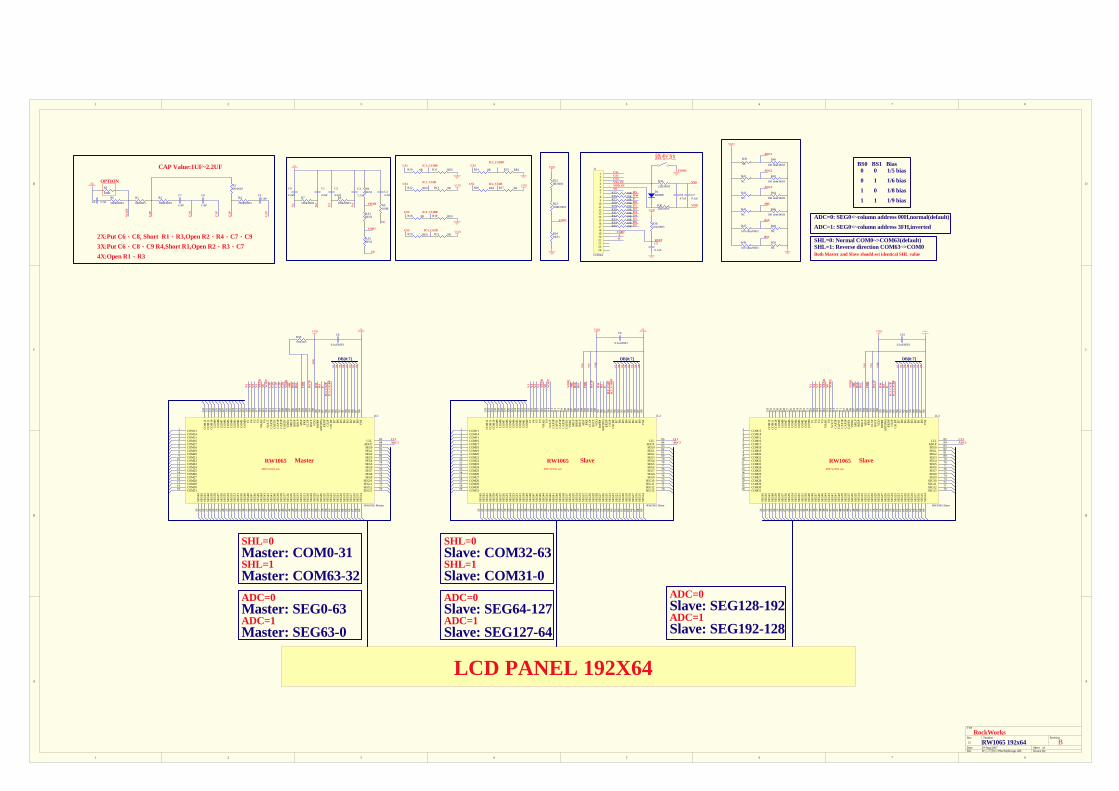


![ROCKWORKS Gulf Coast [re]Build - ww1.prweb.comww1.prweb.com/prfiles/2006/08/21/0000427513/rwdossierforestFINAL... · ROCKWORKS Gulf Coast [re]Build INTRODUCTION Our mission is to](https://static.fdocuments.net/doc/165x107/5aa44e157f8b9a517d8bb593/rockworks-gulf-coast-rebuild-ww1prweb-gulf-coast-rebuild-introduction-our.jpg)

