Anisotropic Hexagonal Boron Nitride Nanomaterials - Synthesis and
Role of Pressure in the Growth of Hexagonal Boron Nitride ThinFilms from Ammonia-BoraneJustin C. Koepke,†,‡,§,□,▼ Joshua D. Wood,†,‡,§,○,▼ Yaofeng Chen,†,‡,§ Scott W. Schmucker,∥
Ximeng Liu,†,‡,§ Noel N. Chang,⊥ Lea Nienhaus,‡,§,⊥,△ Jae Won Do,†,‡,§ Enrique A. Carrion,†,§
Jayan Hewaparakrama,†,§ Aniruddh Rangarajan,†,‡,§ Isha Datye,†,‡,§ Rushabh Mehta,†,‡,§
Richard T. Haasch,# Martin Gruebele,‡,⊥,● Gregory S. Girolami,‡,⊥ Eric Pop,†,¶
and Joseph W. Lyding*,†,‡,§
†Department of Electrical and Computer Engineering, University of Illinois at Urbana−Champaign, Urbana, Illinois 61801, UnitedStates‡Beckman Institute, University of Illinois at Urbana−Champaign, Urbana, Illinois 61801, United States§Micro and Nanotechnology Lab, University of Illinois at Urbana−Champaign, Urbana, Illinois 61801, United States∥U.S. Naval Research Laboratory, Washington, DC 20375, United States⊥Department of Chemistry, University of Illinois at Urbana−Champaign, Urbana, Illinois 61801, United States#Materials Research Laboratory, University of Illinois at Urbana−Champaign, Urbana, Illinois 61801, United States●Department of Physics, University of Illinois at Urbana−Champaign, Urbana, Illinois 61801, United States¶Electrical Engineering, Stanford University, Stanford, California 94305, United States
*S Supporting Information
ABSTRACT: We analyze the optical, chemical, and electricalproperties of chemical vapor deposition (CVD) grown hexagonalboron nitride (h-BN) using the precursor ammonia-borane (H3N−BH3) as a function of Ar/H2 background pressure (PTOT). Filmsgrown at PTOT ≤ 2.0 Torr are uniform in thickness, highlycrystalline, and consist solely of h-BN. At larger PTOT, with constantprecursor flow, the growth rate increases, but the resulting h-BN ismore amorphous, disordered, and sp3-bonded. We attribute thesechanges in h-BN grown at high pressure to incomplete thermolysisof the H3N−BH3 precursor from a passivated Cu catalyst. A similarincrease in h-BN growth rate and amorphization is observed even at low PTOT if the H3N−BH3 partial pressure is initially greaterthan the background pressure PTOT at the beginning of growth. h-BN growth using the H3N−BH3 precursor reproducibly cangive large-area, crystalline h-BN thin films, provided that the total pressure is under 2.0 Torr and the precursor flux is well-controlled.
■ INTRODUCTION
Hexagonal boron nitride (h-BN) is an insulating, two-dimensional (2D) equivalent of graphene. Films of h-BNhave been used as insulating spacers,1 encapsulants,2 substratesfor electronic devices,3,4 corrosion and oxidation-resistantcoatings,5,6 and surfaces for growth of other 2D nanomaterials,such as graphene7 and WS2.
8 Most of these studies employedsmall-area (∼100 μm2) h-BN pieces exfoliated from sintered h-BN crystals,9 limiting technological use of h-BN films.Additionally, unlike graphene, h-BN is difficult to prepare inmonolayer form by exfoliation. The electronegativity differencebetween B and N and the reduced resonance stabilizationrelative to graphene results in electrostatic attractions betweenlayers and in-plane. Consequently, it is more challenging tocontrol h-BN grain size and layer number. Furthermore,
partially ionic B−N bonds can form between neighboring BNlayers, serving to “spot-weld” such layers together.10
Several groups have sought to overcome these limitations byusing chemical vapor deposition (CVD) to grow large-area,monolayer h-BN films.11−22 CVD growth of h-BN has beenaccomplished using various precursors (e.g., ammonia borane,borazine, and diborane) on transition metal substrates (e.g., Cu,Ni,23 Fe,24 Ru,25,26 etc.). Of these h-BN growth substrates, wefocus on Cu, as Cu has a high catalytic activity,27 is inexpensive,and is the typical growth substrate28 for conventional grapheneCVD. Regarding h-BN growth precursors, volatile borazine,B3N3H6, isoelectronic with benzene, is far from an ideal choice,
Received: January 28, 2016Revised: May 9, 2016Published: May 22, 2016
Article
pubs.acs.org/cm
© 2016 American Chemical Society 4169 DOI: 10.1021/acs.chemmater.6b00396Chem. Mater. 2016, 28, 4169−4179
as borazine is hazardous and decomposes quickly even at roomtemperature. While borazine can pyrolyze and dehydrogen-ate23,25,29,30 to generate h-BN films,13,17,19,20,22,31 partialdehydrogenation is common,30 resulting in oligomeric BNcompounds and aperiodic h-BN grain boundaries.13,17 Finally,thin films of h-BN can also be grown from mixtures of diborane(B2H6) and ammonia (NH3),
21 with the drawback thatdiborane is toxic and pyrophoric.In contrast to borazine and diborane, the molecule ammonia-
borane (H3N−BH3) is inexpensive, air stable, and has sufficientvolatility to serve as a CVD precursor for h-BN thinfilms.12,15,16,18,21,32−38 High purity ammonia-borane shows nodecomposition over two months at room temperature,39 and itsvapor pressure has been estimated to be ∼10−4 Torr at roomtemperature.40,41 Heating ammonia-borane generates hydrogenand volatile B- and N-containing species that enable h-BNgrowth; the generated species include monomeric aminoborane(H2N=BH2), borazine, and small amounts of diborane.34,42
However, the growth of h-BN from ammonia-borane, typicallycarried out in the presence of H2, gives variable resultsdepending on the growth temperature,43 substrate rough-ness,44,45 substrate structure,46 position of the growth substraterelative to the precursor source,35,36,43 and precursor flux.12,16
To date, it is unknown how growth pressure affects CVD h-BNgrowth on Cu using ammonia-borane. One can grow h-BNwith large (∼35 μm2) grain sizes under atmospheric pressureCVD conditions, provided that the precursor flux is kept verylow, an electropolished Cu surface is used, and the substratetemperature is kept higher than 1000 °C.45 Nevertheless, littlemechanistic information is available about the CVD growth ofh-BN from ammonia-borane, especially at different growthpressures, although a report suggests that ammonia-boranederived growths on Cu proceed by surface catalysis.16
Here, we examine conditions under which crystalline films ofh-BN can be grown from ammonia-borane and H2 by CVD.We find that low pressure CVD (LPCVD) gives uniform,planar h-BN films, as ascertained by scanning electronmicroscopy (SEM), atomic force microscopy (AFM), X-rayphotoelectron spectroscopy (XPS), Fourier transform infrared(FTIR) spectroscopy, Raman spectroscopy, and scanningtunneling microscopy (STM) and spectroscopy (STS). Whileholding the precursor temperature and carrier gas flows
constant, increasing the growth pressure significantly altersthe properties of the h-BN films, producing thicker, moredisordered films with nonplanar, sp3 components. Further,higher precursor flux conditions in LPCVD growth give thicker,nanocrystalline h-BN films, showing the importance of the ratioof precursor to H2 in h-BN CVD growth. As demonstrated forgraphene growth,47−50 CVD growth of h-BN is sensitive to theAr/H2 background pressure.
■ EXPERIMENTAL SECTIONChemical Vapor Deposition (CVD) of Hexagonal Boron
Nitride (h-BN) on Cu Foil. Growth experiments were conducted in aretrofitted Atomate CVD furnace (see Figure S1). Care was taken toeliminate adventitious carbon sources from the growth chamber,otherwise h-BNC69 or defective G/h-BN heterostructures resulted; thepresence of these impurity phases was detected by Raman spectros-copy. The substrates were 0.001 in thick (0.0254 mm) 99.8% purityCu foils (Alfa Aesar), which were rinsed before use with a 10:1 H2O/HCl solution as previously described51−53 and annealed for 2 h underAr/H2 (500 sccm Ar/100 sccm H2) at 1000 °C. Basic copper (BC) ofsimilar purity54 was used a Cu substrate for some growths; wedesignated these substrates accordingly. The annealing step increasedthe Cu grain size and lowered the number of BN nucleation sites.44,45
The precursor H3N−BH3 (Aldrich) was transferred under N2 into astainless steel ampule, minimizing water exposure of the hygroscopicH3N−BH3. Occasionally, a different H3N−B3H supplier was used(Boron Specialties) with similar results. To transport the precursorinto the furnace, the ampule was heated to ∼95 °C, and volatilizedmaterial was swept into the furnace by a 4:1 Ar/H2 carrier. The h-BNfilms were grown at 1000 °C in an Ar/H2 background at the differentpressures indicated. After 25 min of film growth, the samples werecooled at ∼20 °C min−1 under Ar at a flow rate of 500 sccm. See theSupporting Information for further discussion of the conditions thatresult in a high mass (HM) flux for the precursor temperatures used.For further characterization, the h-BN films were transferred from theCu substrate to 90 nm SiO2/Si wafers using methodologies detailedelsewhere.53,55
Sample Annealing after Transfer. Post-transfer annealing of thesamples to remove polymer residues from the poly(methylmethacrylate) or polycarbonate transfer handles also used the samefurnace as h-BN growth, using a quartz tube dedicated to sampleannealing. Attempts to anneal transferred h-BN films under conditionssimilar to those used for annealing graphene, namely, 1 h in Ar/H2 at400 °C, led to pitting and etching of the films, as has been reported.22
Therefore, post-transfer sample anneals were carried out in air at 550
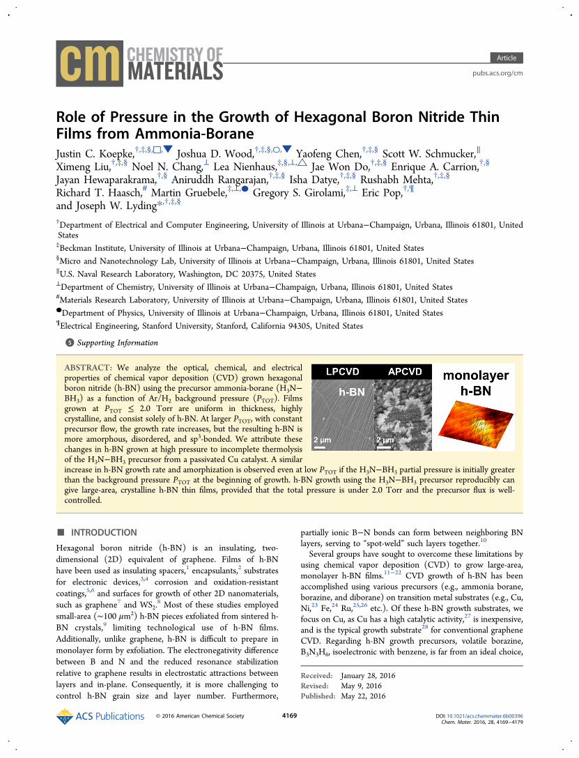
Figure 1. Scanning electron microscopy (SEM) imaging of h-BN on Cu at different pressures. Low-pressure h-BN growth (a) at a large-scale and (b)at a small-scale, revealing a planar h-BN film with protrusions from Cu step flow66 and h-BN wrinkles. (c) Higher pressure growth, showing a loss ofthe Cu hillock morphology and an increase in charging. (d) Medium-pressure growth, with similar morphology as (c). Atmospheric pressure h-BNgrowth at a large-scale (e) and a small-scale (f), with polymeric features evident. These features suggest a breakdown in Cu-mediated catalysis.
Chemistry of Materials Article
DOI: 10.1021/acs.chemmater.6b00396Chem. Mater. 2016, 28, 4169−4179
4170
°C as described by others;56 h-BN is known to be oxidation resistantunder these conditions.6,57
Lithographic Patterning. To obtain lithographically patterned h-BN samples, we defined a square array in the h-BN film by UVphotolithography, using a conventional TEM grid as a mask and an O2plasma to etch. Polymethylglutarimide (PMGI; MicroChem) was spunat 3500 rpm for 30 s and cured at 165 °C for 5 min. Shipley 1813photoresist (MicroChem) was spun on top of the cured PMGI at 5000rpm for 30 s. The photoresist was soft baked at 110 °C for 70 s, floodexposed to UV (i-line, 365 nm) through a TEM grid for 4 s on a Karl-Suss aligner, and developed for 50 s in MF-319 (MicroChem). Usingthe patterned photoresist as a mask, we etched the samples in an O2plasma for 1 min under 20 sccm of O2 at 100 mTorr throttle pressureand ∼90 W power. After the O2 etch, the samples were soaked in hot(∼50 °C) remover PG (nominally n-methylpyrrolidone) for 20 min.Scanning Electron Microscopy (SEM). The h-BN films were
examined immediately after growth on the Cu foil by an FEIenvironmental SEM operating at 5 kV. All images were taken using anultrahigh-definition mode, which increases the dwell time and thebeam current. We maintained similar values for the brightness andcontrast during image collection, so that the images in Figure 1 can becompared.Atomic Force Microscopy (AFM). Most AFM images were
collected in tapping mode with ∼300 kHz Si cantilevers on a BrukerAFM with a Dimension IV controller. Scan rates were slower than 2Hz, and sampling was at least 512 samples per line by 512 lines; mostof the scans were 1024 × 1024 images. Images with low noise andstable phase were selected for analysis. Images were destreaked, planefit, and analyzed using Gwyddion.58 Root mean square (RMS)roughness values were determined using Gwyddion and by means ofan algorithm written in MATLAB. Autocorrelation values were alsodetermined and fit in Gwyddion. Some AFM images were taken on anAsylum Research MFP-3D AFM in tapping mode using ∼300 kHzresonant frequency Si cantilevers (NSG30 AFM tips from NT-MDT).X-ray Photoelectron Spectroscopy (XPS). A Kratos ULTRA
XPS with a monochromatic Kα Al X-ray line was used to collect data.We fitted all subpeaks with Shirley backgrounds and Gaussian−Lorentzian (GL) mixing. The amount of GL character was optimized(i.e., not fixed) in our fits, so as to lower the chi-squared value and berepresentative of the true chemical state of the subpeak in question. Toprevent sample charging, samples were mounted on a conducting stageusing conductive tape or a metal clamp and were exposed to a floodgun during data collection. All core levels were charge corrected to theadventitious sp2/sp3 C 1s peak at 284.8 eV.Fourier Transform Infrared (FTIR) Spectroscopy. FTIR spectra
of the h-BN films while still on the Cu foil growth substrate werecollected on a Thermo Nicolet NEXUS 670 FTIR with a Smart iTRattenuated total reflectance (ATR) sampling accessory with a ZnSewindow. All spectra were acquired in air. Before measuring an h-BNspectrum, an air background with no sample on the ZnSe window wascollected and used. Each spectrum was the sum of 256 scans at least 2wavenumber resolution.Raman Spectroscopy. Raman spectra were acquired on a Horiba
LabRAM HR 3D-capable imaging system at 532 nm. Data werecollected with an 1800 lines/mm grating, a 100× (0.8 NA) objective,and a power level below ∼10 mW. The Raman cross-section59 of h-BNis low at 532 nm and, to improve signal-to-noise ratio and avoid thefluorescent background of the Cu foil, the Raman spectra measure-ments were performed on h-BN films that had been transferred toSiO2/Si substrates. Raman mapping data were acquired around the E2gband position (∼1370 cm−1)60,61 using a minimum array of 100Raman point spectra at ∼5 μm point spacing. Each spectrum consistedof an average of four to six individual measurements made at the samelocation, each with a 45 to 60 s acquisition time. The E2g mode and thehigher order (∼1450 cm−1) Si third order TO phonon mode (3TO)mode intrinsic to the SiO2/Si substrate were each fit with a singleLorentzian function using a Levenberg−Marquardt fitting algorithm inFityk.62
Scanning Tunneling Microscopy (STM). Our experimentsemployed a home-built, room-temperature ultrahigh vacuum scanning
tunneling microscope (UHV-STM)63 with a base pressure of ∼3 ×10⁻¹¹ Torr and electrochemically etched W and PtIr tips. Some of thetips were sharpened using field-directed sputter sharpening.64 Wescanned the samples in constant-current mode, in which the feedbackelectronics controlled the tip height to maintain a current set point,while rastering the tip across the surface. The STM tip was groundedthrough a current amplifier, and the tunneling bias was applied to thesample. For the constant-spacing scanning tunneling spectroscopy(STS) measurements, the tip was stopped at predetermined locations,the tip feedback was turned off, and the tip−sample bias was sweptthrough the specified range while recording the tunneling current.
Ultraviolet−Visible (UV−vis) Absorption Spectroscopy. AShimadzu UV-1650 PC instrument was used to collect UV−vistransmission spectra at an incidence angle of approximately ∼60°. h-BN films were transferred onto UV-transparent quartz slides (SPI, partnumber 01020-AB). The transmission spectra were acquired withrespect to a blank quartz slide reference.
■ RESULTS
We have grown thin films of h-BN by CVD on polycrystallineCu foils at ∼1000 °C. Our growths last for 25 min in thepresence of H2 using the precursor ammonia-borane. Althoughtemperatures above ∼1170 °C are required to producecrystalline h-BN from ammonia-borane in the solid state,34,42
metal catalysts can reduce this threshold to the ∼1000 °Ctemperatures used in our experiments.26,65
The precursor reservoir is kept at ∼95 °C during depositionruns. At this temperature ammonia-borane decomposes slowlyto generate primarily H2 and monomeric aminoborane, withnegligible (i.e., undetected by mass spectrometry) amounts ofborazine and diborane.34,42 Typically, upon opening the valveto the precursor to begin growth, the pressure in the chamberincreases slightly by ∼0.05 Torr; this pressure spike dissipatesover about ∼1 min. For some of the deposition runs, especiallyif the reservoir temperature is ∼100 °C, the pressure increaseupon opening the valve to the reservoir is somewhat higher (upto several Torr), undoubtedly due to buildup of H2 andammonia-borane decomposition products in the reservoir. Werefer to these higher ammonia-borane partial pressure spikes ashigh mass (HM) flow conditions (see Supporting Informationfor further discussion).A 4:1 mixture of Ar:H2, with flow rates of either 400:100
standard cubic centimeters per minute (sccm) or 200:50 sccm,is used as a carrier gas to transport the precursor to the growthchamber. Three pressure regimes were investigated: (1) lowpressure CVD conditions (LPCVD), for which the total Ar/H2
background pressure, PTOT, is 2 Torr (PH2= 0.4 Torr) or less;
(2) medium pressure conditions, with either PTOT = 20 Torr(PH2
= 4 Torr) or PTOT = 200 Torr (PH2= 40 Torr); and (3)
atmospheric CVD conditions (APCVD), for which PTOT = 760Torr (PH2
= 152 Torr). We estimate the PH2/PH3N−BH3
ratio over
the growth surface is ∼50 for our LPCVD conditions. The PH2/
PH3N−BH3ratio increases for higher PTOT values and decreases
for HM flow conditions.Figure 1a shows a large-area SEM image of an h-BN film
grown on Cu under LPCVD conditions. The closely spaced(∼0.025 μm) striations running at approximately a −20° anglefrom vertical in the image indicate the step flow direction of theunderlying Cu surface. These steps, which result from themismatch in thermal expansion coefficients between h-BN andCu, form only if the overlayer is planar and has a well-orderedcrystalline structure.66 The faint striations running diagonallyfrom upper right to lower left are attributed to thermally
Chemistry of Materials Article
DOI: 10.1021/acs.chemmater.6b00396Chem. Mater. 2016, 28, 4169−4179
4171
induced wrinkles in the h-BN overlayer.13,16,32,36,67 Figure 1b isa smaller-area SEM image of another region of the sameLPCVD grown h-BN sample. The prominent feature thatapproximately bisects the image vertically is a Cu grainboundary. Here, an h-BN wrinkle crosses the Cu grainboundary; similar behavior has been seen for graphene.28
When growth is conducted at medium pressures (≥20 Torr)of background gas, the Cu step flow features and h-BN wrinklesare absent and the surface appears morphologically rough(Figure 1c). There is also a high density of nanoparticles in theimage. Similar results are obtained at a growth pressure of 200Torr (Figure 1d); the surface is rough, and Cu step flowfeatures are absent. Under APCVD conditions, the h-BN film isnonplanar and exhibits disordered surface features in both thelarger-area (Figure 1e) and smaller-area (Figure 1f) SEMimages. There are no previous reports of such disorderedsurface features for APCVD grown h-BN. The lack of obviousCu step flow features and h-BN wrinkles suggests that this filmis thicker than those grown under LPCVD conditions. Foradditional SEM images of partially grown, submonolayer h-BN,LPCVD, and APCVD grown h-BN, see Figures S3 and S4.Figure 2 shows AFM images of the h-BN films as a function
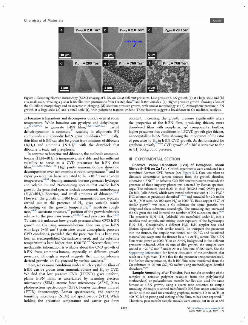
of the Ar/H2 background pressure (PTOT), along with heightprofiles across a film boundary generated by lithographicetching. Figure 2a shows an h-BN film grown at PTOT = 1.2Torr (LPCVD regime); the film edge is indicated by thedashed, blue line. The film thickness of 0.8 ± 0.1 nm
corresponds well to 1 to 2 h-BN layers,9,10 and the root-mean-square (RMS) roughness is 0.58 nm. The larger RMSroughness relative to the film thickness likely stems fromentrapped water and polymeric contaminants introduced in theh-BN film transfer.53 When a film grown under similar LPCVDconditions (PTOT = 2.0 Torr) is annealed in Ar/H2 at 400 °C,the film becomes smoother (0.45 nm RMS roughness) andetch tracks are formed (Figure 2b). The step height of the filmafter annealing is 1.0 ± 0.3 nm.Figure 2c and 2d shows AFM topographs of two different
films also grown under LPCVD conditions (2.0 Torr), exceptthat there was a higher than normal flux from the reservoirduring growth (HM conditions). The higher flux was aconsequence of keeping the reservoir at ∼100 °C versus 95 °C;at the higher temperature, the precursor evolves up to 100times more H2 and volatile B- and N-containing species (seeSupporting Information for further discussion). The resultingh-BN films are both thicker (3.2 ± 1.4 nm) and rougher (1.51nm RMS roughness) than those grown under LPCVDconditions when the precursor reservoir is not overheated.When grown at intermediate background pressures of Ar/H2
gas (PTOT = 20 Torr) but at normal flux from the reservoir, thefilms are also thick (3.4 ± 0.6 nm) and rough (3.20 nm RMSroughness). These values resemble those for the sample grownat 2.0 Torr under HM conditions, underscoring the importanceof controlling the precursor flux during growth.
Figure 2. Changes in h-BN film morphology due to precursor mass flow and growth pressure. (a) Atomic force microscopy (AFM) images oftransferred and lithographically patterned (blue line) h-BN on SiO2 growth at low pressure (1.2 Torr). (b) Low pressure (2.0 Torr) h-BN growthwith improved precursor mass flow control showing smoother morphology. (c, d) AFM images of transferred h-BN on SiO2 grown at low pressure(2.0 Torr) but with a high mass (HM) flow of H3N−BH3. The HM condition gives a more nanocrystalline h-BN film, as seen in the overlaid heightprofile. (e) Medium pressure (20 Torr) h-BN growth with heightened H3N−BH3 catalysis on a former Cu annealing twin. AFM image (f) andheight profile (g) for lithographically patterned (blue line) h-BN grown at medium pressure (200 Torr). Patterned large-area (h) AFM image for h-BN grown at atmospheric pressure (760 Torr). The APCVD grown film is highly inhomogeneous and rough, with polymeric depressionscorresponding to the features seen in SEM. (i) h-BN film thickness versus growth pressure, showing thin h-BN films at LPCVD.
Chemistry of Materials Article
DOI: 10.1021/acs.chemmater.6b00396Chem. Mater. 2016, 28, 4169−4179
4172
For intermediate growth pressures (PTOT = 20 Torr), the h-BN thin films template Cu substrate morphology, as apparentfrom the former Cu annealing twin shown in the topograph ofFigure 2e. Vicinal Cu surfaces are known to lead to moredefective, thicker graphene growth,54 potentially explaining theenhanced h-BN growth on the twin. At higher growth pressures(PTOT = 200 Torr), the film in Figure 2f and 2g has a stepheight of 10.1 ± 0.9 nm (1.53 nm RMS roughness), with largeprotrusions from transfer induced PMMA residuals.53 UnderAPCVD conditions (Figure 2h), the h-BN films are rougherstill (1.64 nm RMS roughness) and possess inhomogeneousdepressions with contours corresponding to the morphologyseen in the SEM images (Figure 1e and 1f).The h-BN film thickness for different growth pressures
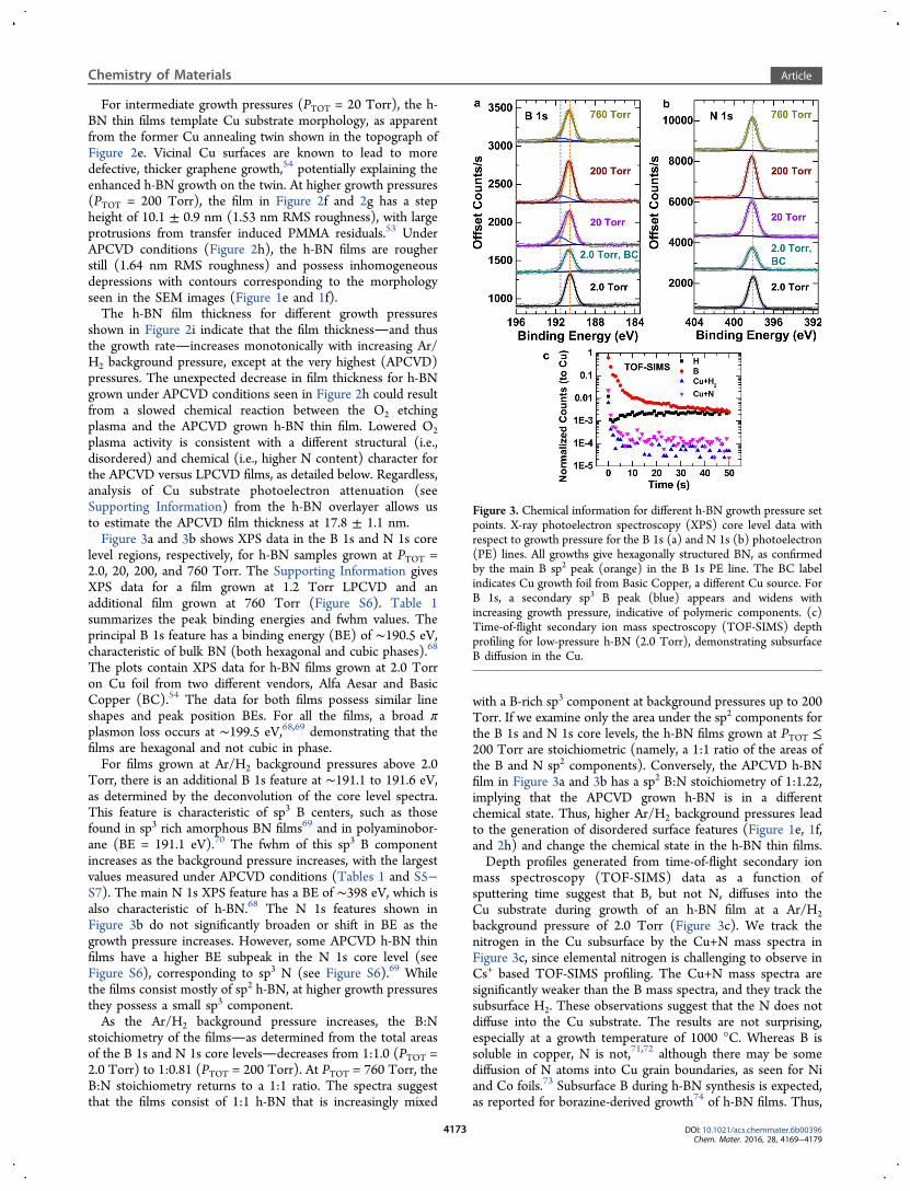
shown in Figure 2i indicate that the film thicknessand thusthe growth rateincreases monotonically with increasing Ar/H2 background pressure, except at the very highest (APCVD)pressures. The unexpected decrease in film thickness for h-BNgrown under APCVD conditions seen in Figure 2h could resultfrom a slowed chemical reaction between the O2 etchingplasma and the APCVD grown h-BN thin film. Lowered O2plasma activity is consistent with a different structural (i.e.,disordered) and chemical (i.e., higher N content) character forthe APCVD versus LPCVD films, as detailed below. Regardless,analysis of Cu substrate photoelectron attenuation (seeSupporting Information) from the h-BN overlayer allows usto estimate the APCVD film thickness at 17.8 ± 1.1 nm.Figure 3a and 3b shows XPS data in the B 1s and N 1s core
level regions, respectively, for h-BN samples grown at PTOT =2.0, 20, 200, and 760 Torr. The Supporting Information givesXPS data for a film grown at 1.2 Torr LPCVD and anadditional film grown at 760 Torr (Figure S6). Table 1summarizes the peak binding energies and fwhm values. Theprincipal B 1s feature has a binding energy (BE) of ∼190.5 eV,characteristic of bulk BN (both hexagonal and cubic phases).68
The plots contain XPS data for h-BN films grown at 2.0 Torron Cu foil from two different vendors, Alfa Aesar and BasicCopper (BC).54 The data for both films possess similar lineshapes and peak position BEs. For all the films, a broad πplasmon loss occurs at ∼199.5 eV,68,69 demonstrating that thefilms are hexagonal and not cubic in phase.For films grown at Ar/H2 background pressures above 2.0
Torr, there is an additional B 1s feature at ∼191.1 to 191.6 eV,as determined by the deconvolution of the core level spectra.This feature is characteristic of sp3 B centers, such as thosefound in sp3 rich amorphous BN films69 and in polyaminobor-ane (BE = 191.1 eV).70 The fwhm of this sp3 B componentincreases as the background pressure increases, with the largestvalues measured under APCVD conditions (Tables 1 and S5−S7). The main N 1s XPS feature has a BE of ∼398 eV, which isalso characteristic of h-BN.68 The N 1s features shown inFigure 3b do not significantly broaden or shift in BE as thegrowth pressure increases. However, some APCVD h-BN thinfilms have a higher BE subpeak in the N 1s core level (seeFigure S6), corresponding to sp3 N (see Figure S6).69 Whilethe films consist mostly of sp2 h-BN, at higher growth pressuresthey possess a small sp3 component.As the Ar/H2 background pressure increases, the B:N
stoichiometry of the filmsas determined from the total areasof the B 1s and N 1s core levelsdecreases from 1:1.0 (PTOT =2.0 Torr) to 1:0.81 (PTOT = 200 Torr). At PTOT = 760 Torr, theB:N stoichiometry returns to a 1:1 ratio. The spectra suggestthat the films consist of 1:1 h-BN that is increasingly mixed
with a B-rich sp3 component at background pressures up to 200Torr. If we examine only the area under the sp2 components forthe B 1s and N 1s core levels, the h-BN films grown at PTOT ≤200 Torr are stoichiometric (namely, a 1:1 ratio of the areas ofthe B and N sp2 components). Conversely, the APCVD h-BNfilm in Figure 3a and 3b has a sp2 B:N stoichiometry of 1:1.22,implying that the APCVD grown h-BN is in a differentchemical state. Thus, higher Ar/H2 background pressures leadto the generation of disordered surface features (Figure 1e, 1f,and 2h) and change the chemical state in the h-BN thin films.Depth profiles generated from time-of-flight secondary ion
mass spectroscopy (TOF-SIMS) data as a function ofsputtering time suggest that B, but not N, diffuses into theCu substrate during growth of an h-BN film at a Ar/H2background pressure of 2.0 Torr (Figure 3c). We track thenitrogen in the Cu subsurface by the Cu+N mass spectra inFigure 3c, since elemental nitrogen is challenging to observe inCs+ based TOF-SIMS profiling. The Cu+N mass spectra aresignificantly weaker than the B mass spectra, and they track thesubsurface H2. These observations suggest that the N does notdiffuse into the Cu substrate. The results are not surprising,especially at a growth temperature of 1000 °C. Whereas B issoluble in copper, N is not,71,72 although there may be somediffusion of N atoms into Cu grain boundaries, as seen for Niand Co foils.73 Subsurface B during h-BN synthesis is expected,as reported for borazine-derived growth74 of h-BN films. Thus,
Figure 3. Chemical information for different h-BN growth pressure setpoints. X-ray photoelectron spectroscopy (XPS) core level data withrespect to growth pressure for the B 1s (a) and N 1s (b) photoelectron(PE) lines. All growths give hexagonally structured BN, as confirmedby the main B sp2 peak (orange) in the B 1s PE line. The BC labelindicates Cu growth foil from Basic Copper, a different Cu source. ForB 1s, a secondary sp3 B peak (blue) appears and widens withincreasing growth pressure, indicative of polymeric components. (c)Time-of-flight secondary ion mass spectroscopy (TOF-SIMS) depthprofiling for low-pressure h-BN (2.0 Torr), demonstrating subsurfaceB diffusion in the Cu.
Chemistry of Materials Article
DOI: 10.1021/acs.chemmater.6b00396Chem. Mater. 2016, 28, 4169−4179
4173
low pressure, ammonia-borane derived h-BN syntheses proceedby both bulk precipitation and surface catalysis. Further, thesefindings are consistent the recent observation of bulkprecipitation for CVD h-BN growth on Ni and Co foils.73,75
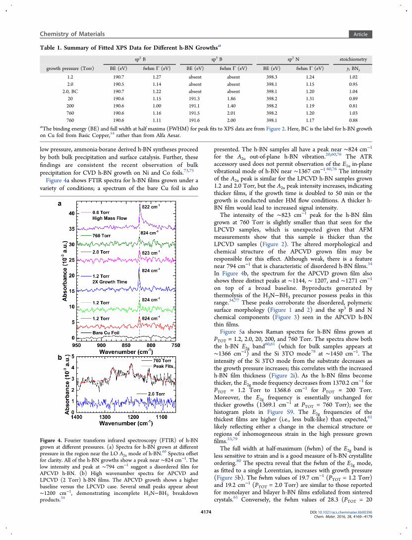
Figure 4a shows FTIR spectra for h-BN films grown under avariety of conditions; a spectrum of the bare Cu foil is also
presented. The h-BN samples all have a peak near ∼824 cm−1
for the A2u out-of-plane h-BN vibration.20,60,76 The ATRaccessory used does not permit observation of the E1u in-planevibrational mode of h-BN near ∼1367 cm−1.60,76 The intensityof the A2u peak is similar for the LPCVD h-BN samples grown1.2 and 2.0 Torr, but the A2u peak intensity increases, indicatingthicker films, if the growth time is doubled to 50 min or thegrowth is conducted under HM flow conditions. A thicker h-BN film would lead to increased signal intensity.The intensity of the ∼823 cm−1 peak for the h-BN film
grown at 760 Torr is slightly smaller than that seen for theLPCVD samples, which is unexpected given that AFMmeasurements show that this sample is thicker than theLPCVD samples (Figure 2). The altered morphological andchemical structure of the APCVD grown film may beresponsible for this effect. Although weak, there is a featurenear 794 cm−1 that is characteristic of disordered h-BN films.34
In Figure 4b, the spectrum for the APCVD grown film alsoshows three distinct peaks at ∼1144, ∼ 1207, and ∼1271 cm−1
on top of a broad baseline. Byproducts generated bythermolysis of the H3N−BH3 precursor possess peaks in thisrange.34,77 These peaks corroborate the disordered, polymericsurface morphology (Figure 1 and 2) and the sp3 B and Nchemical components (Figure 3) seen in the APCVD h-BNthin films.Figure 5a shows Raman spectra for h-BN films grown at
PTOT = 1.2, 2.0, 20, 200, and 760 Torr. The spectra show boththe h-BN E2g band60,61 (which for bulk samples appears at∼1366 cm−1) and the Si 3TO mode78 at ∼1450 cm−1. Theintensity of the Si 3TO mode from the substrate decreases asthe growth pressure increases; this correlates with the increasedh-BN film thickness (Figure 2i). As the h-BN films becomethicker, the E2g mode frequency decreases from 1370.2 cm−1 forPTOT = 1.2 Torr to 1368.6 cm−1 for PTOT = 200 Torr.Moreover, the E2g frequency is essentially unchanged forthicker growths (1369.1 cm−1 at PTOT = 760 Torr); see thehistogram plots in Figure S9. The E2g frequencies of thethickest films are higher (i.e., less bulk-like) than expected,61
likely reflecting either a change in the chemical structure orregions of inhomogeneous strain in the high pressure grownfilms.33,79
The full width at half-maximum (fwhm) of the E2g band isless sensitive to strain and is a good measure of h-BN crystalliteordering.80 The spectra reveal that the fwhm of the E2g mode,as fitted to a single Lorentzian, increases with growth pressure(Figure 5b). The fwhm values of 19.7 cm−1 (PTOT = 1.2 Torr)and 19.2 cm−1 (PTOT = 2.0 Torr) are similar to those reportedfor monolayer and bilayer h-BN films exfoliated from sinteredcrystals.61 Conversely, the fwhm values of 28.3 (PTOT = 20
Table 1. Summary of Fitted XPS Data for Different h-BN Growthsa
sp2 B sp3 B sp2 N stoichiometry
growth pressure (Torr) BE (eV) fwhm Γ (eV) BE (eV) fwhm Γ (eV) BE (eV) fwhm Γ (eV) y, BNy
1.2 190.7 1.27 absent absent 398.3 1.24 1.022.0 190.5 1.14 absent absent 398.1 1.15 0.95
2.0, BC 190.7 1.22 absent absent 398.1 1.20 1.0420 190.6 1.15 191.3 1.86 398.2 1.31 0.89200 190.6 1.00 191.1 1.40 398.2 1.19 0.81760 190.6 1.16 191.5 2.01 398.2 1.20 1.03760 190.6 1.11 191.6 2.00 398.1 1.17 0.88
aThe binding energy (BE) and full width at half maxima (FWHM) for peak fits to XPS data are from Figure 2. Here, BC is the label for h-BN growthon Cu foil from Basic Copper,54 rather than from Alfa Aesar.
Figure 4. Fourier transform infrared spectroscopy (FTIR) of h-BNgrown at different pressures. (a) Spectra for h-BN grown at differentpressure in the region near the LO A2u mode of h-BN.
60 Spectra offsetfor clarity. All of the h-BN growths show a peak near ∼824 cm−1. Thelow intensity and peak at ∼794 cm−1 suggest a disordered film forAPCVD h-BN. (b) High wavenumber spectra for APCVD andLPCVD (2 Torr) h-BN films. The APCVD growth shows a higherbaseline versus the LPCVD case. Several small peaks appear about∼1200 cm−1, demonstrating incomplete H3N−BH3 breakdownproducts.34
Chemistry of Materials Article
DOI: 10.1021/acs.chemmater.6b00396Chem. Mater. 2016, 28, 4169−4179
4174
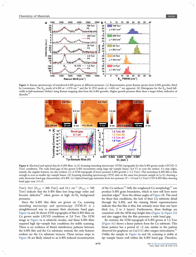
Torr), 24.5 (PTOT = 200 Torr), and 25.1 cm−1 (PTOT = 760Torr) indicate that the h-BN films lose long-range order andbecome defective80 when grown at high Ar/H2 backgroundpressures.Since the h-BN thin films are grown on Cu, scanning
tunneling microscopy and spectroscopy (STM/S) is astraightforward way to measure their electronic band gaps.Figure 6a and 6b shows STM topographs of thin h-BN films onCu grown under LPCVD conditions at 2.0 Torr. The STMimage in Figure 6a is relatively streaky, and these h-BN filmsrequired high tip−sample bias conditions for stable scanning.There is no evidence of Moire interference patterns betweenthe h-BN film and the Cu substrate; instead, the only featuresevident are the Cu substrate terraces. These terrace steps inFigure 6b are likely related to an h-BN induced reconstruction
of the Cu surfaces.66 Still, the roughened Cu morphology54 canproduce h-BN grain boundaries, which in turn will have morearmchair edges81 from the obtuse angles of Figure 6b. The needfor these bias conditions, the lack of finer Cu substrate detailthrough the h-BN, and the missing Moire superstructuresindicate that this film is thin, but certainly more than one layerthick (i.e., 2 to 3 layers). Furthermore, these findings areconsistent with the AFM step height data (Figure 2i, Figure S5)and also suggest that the film possesses a wide band gap.By contrast, the STM topograph of h-BN grown at 1.2 Torr
(Figure 6c) shows a linear pattern from the Cu substrate. Thislinear pattern has a period of ∼2 nm, similar to the patternobserved for graphene on Cu(111) after oxygen intercalation.82
Unlike the sample in Figure 6a and 6b, scanning is stable attip−sample biases well within the h-BN band gap. Therefore,
Figure 5. Raman spectroscopy of transferred h-BN grown at different pressures. (a) Representative point Raman spectra from h-BN growths, fittedby Lorentzians. The E2g mode of h-BN at ∼1370 cm−1 and the Si 3TO mode at ∼1450 cm−1 are apparent. (b) Histograms for the E2g band full-width at half-maximum (fwhm) using Raman mapping data from the h-BN growths. Higher growth pressure films show a larger fwhm, indicative ofdisorder.80
Figure 6. Electrical and optical data for h-BN films. (a, b) Scanning tunneling microscopy (STM) topographs for thin h-BN grown under LPCVD (2Torr) conditions. The wide band gap of the grown h-BN necessitates using large tip−sample biases (±4 V) to scan the surface. Cu step edges,namely, the angular features, are also evident. (c) A STM topograph of lower pressure h-BN growth (∼1.2 Torr). This monolayer h-BN film is thinenough to scan at smaller tip−sample biases. (d) Scanning tunneling spectroscopy (STS) data on the same low-pressure sample in (a, b), showing awide electronic band gap characteristic of h-BN. (e) Optical band gap extraction from low pressure (P = 1.0 and 1.2 Torr) CVD h-BN films showingband gaps near 5.4 eV.
Chemistry of Materials Article
DOI: 10.1021/acs.chemmater.6b00396Chem. Mater. 2016, 28, 4169−4179
4175
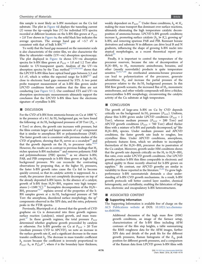
this sample is most likely an h-BN monolayer on the Cu foilsubstrate. The plot in Figure 6d displays the tunneling current(I) versus the tip−sample bias (V) for individual STS spectrarecorded at different locations on the h-BN film grown at PTOT= 2.0 Torr shown in Figure 6a; the solid black line indicates theaverage spectrum. The average band gap of ∼5.7 eV isconsistent with that of bulk h-BN.9,21
To verify that the band gap measured on the nanometer scaleis also characteristic of the entire film, we also characterize thefilms by ultraviolet−visible (UV−vis) absorption spectroscopy.The plot displayed in Figure 6e shows UV−vis absorptionspectra for h-BN films grown at PTOT = 1.0 and 1.2 Torr aftertransfer to UV-transparent quartz. Analysis of the UV−visabsorption spectra by the Tauc method12,15,20,21,83 shows thatthe LPCVD h-BN films have optical band gaps between 5.3 and5.5 eV, which is within the expected range for h-BN9,21 andclose to electronic band gaps measured by STS. A two pointprobe transport measurement of an h-BN film grown underLPCVD conditions further confirms that the films are notconducting (see Figure S11). Our combined STS and UV−visabsorption spectroscopic measurements ultimately support theconclusion that the LPCVD h-BN films have the electronicsignature of crystalline h-BN.
■ DISCUSSION
For the CVD of h-BN from ammonia-borane on Cu at 1000 °Cin the presence of a 4:1 Ar/H2 background gas, we have foundthe following: at Ar/H2 background pressures of 20 Torr (PH2
=4 Torr) or above, the growth rate increases with pressure, butthe films contain larger and larger amounts of a sp3 componentthat is similar to amorphous BN or polyaminoborane (PAB).The faster growth rate is consistent with previous studies of theCVD of graphene, showing that H2 serves as a cocatalyst
49 andthat the growth depends on the H2 to precursor ratio.49,50
However, the results are in contrast to previous findings that H2etches spurious h-BN nucleation22 and removes polymeric PABand polyiminoborane (PIB) species,84 as we observe h-BN,PAB, and PIB compounds in h-BN films grown at high Ar/H2background pressure. We can reconcile the contrastingobservations by proposing that, at the higher H2 pressures,the faster h-BN growth rates cause the Cu foil to becomequickly covered, so that its catalytic activity is suppressed. As aresult, the precursor does not completely decompose on top ofthe already deposited h-BN layers. In the absence of a catalyst,growth of h-BN from H3N−BH3 requires very high temper-atures (∼1500 °C).34 Incomplete decomposition of the H3N−BH3 precursor
34,77 explains several of the properties of the h-BN samples grown at a Ar/H2 background pressure of 760Torr: the amorphous, disordered surface morphology, the sp3
components observed in the XPS data, and the extra, polymericpeaks in the FTIR spectra.Previously, Bhaviripudi et al. showed that the growth of CVD
graphene on Cu is demarcated into three growth regimes:surface reaction (catalysis), mixed growth, and mass trans-port.47 In these growth regimes, the total pressure PTOTdetermined whether graphene growth proceeded by catalysisor otherwise. For h-BN growths on Cu at PTOT > 20 Torr(medium pressure CVD to APCVD), we note an increase inthe surface growth rate Ks and a significant decrease in the masstransfer coefficient hg. The decrease in mass transfer coefficienthg occurs because the coefficient is inversely proportional toPTOT: hG ∝ PTOT
−1 δ−1, where δ is the boundary layer thickness,
weakly dependent on PTOT.47 Under these conditions, hg ≪ Ks,
making the mass transport flux dominant over surface reactions,ultimately eliminating the high temperature catalytic decom-position of ammonia-borane. LPCVD h-BN growth conditionsincrease hg, promoting surface catalysis (hg ≫ Ks), growing sp
2
h-BN, and removing spurious PAB and PIB. Remnant boranederivatives and substrate N in-diffusion can drive local B and Ngradients, influencing the shape of growing h-BN nuclei intoatypical morphologies, as a recent theoretical report pre-dicted.85
Finally, it is important to control the temperature of theprecursor reservoir, because the rate of decomposition ofH3N−BH3 to H2, monomeric aminoborane, borazine, andother (mostly nonvolatile) products is quite temperaturesensitive.34,42,77,86 An overheated ammonia-borane precursorcan lead to polymerization of the precursor, generateadventitious H2, and increase the partial pressure of theprecursor relative to the Ar/H2 background pressure. In thisHM flow growth scenario, the increased flux of H2, monomericaminoborane, and other volatile compounds will drive a thicker,nanocrystalline h-BN morphology, circumventing the catalyticactivity of the Cu substrate at high temperature.
■ CONCLUSIONThe growth of large-area h-BN on Cu by CVD dependscritically on the background Ar/H2 pressure (PTOT). Uniform,planar thin h-BN grows under LPCVD conditions (PTOT = 2Torr), whereas medium pressure (PTOT = 200 Torr) andAPCVD growth conditions (PTOT = 760 Torr) afford thickerfilms with a mixture of h-BN and partially decomposed, sp3 likeH3N−BH3 species. Under medium pressure and APCVDconditions, the faster growth rate leads to rougher, lesscrystalline films. Under APCVD conditions, amorphous,polymeric features form, which we attribute to incompletethermolysis of the H3N−BH3 precursor due to passivation ofthe Cu catalyst. Moreover, growth under HM conditions showsthat the growth rate depends critically on the H2 to H3N−BH3flux ratio, even under LPCVD growth conditions. Our LPCVDgrowths produce h-BN thin films comparable in electronic andoptical quality to those recently observed for h-BN grown onsapphire.87 By contrast, our APCVD growths are similar invariability to those reported in the literature.21,44 To grow high-performance h-BN nanomaterials demands a clear under-standing of h-BN CVD growth mechanisms. As a result, h-BNgrowth protocols will better control layer number, chemicalheterogeneity, and crystallinity, enabling the fabrication of largearea, electronic and encapsulatory h-BN heterostructures.
■ ASSOCIATED CONTENT*S Supporting InformationThe Supporting Information is available free of charge on theACS Publications website at DOI: 10.1021/acs.chemma-ter.6b00396.
Additional discussion of the high mass flow (HM)growth conditions, an image of the furnace setup,characterization of the h-BN films including AFMcontours of the film step heights, a table summarizingthe RMS roughness data for the AFM images, furtherXPS data and details of the peak fits for the differentgrowth pressures, Raman histograms of the E2g peakposition for different growth pressures, and a comparisonof the Raman data from LPCVD grown h-BN films with
Chemistry of Materials Article
DOI: 10.1021/acs.chemmater.6b00396Chem. Mater. 2016, 28, 4169−4179
4176
normal precursor flux and under HM growth conditions(PDF)
■ AUTHOR INFORMATIONCorresponding Author*E-mail: [email protected] Addresses□J.C.K.: Sandia National Laboratories, P.O. Box 5800,Albuquerque, NM 87185○J.D.W.: Department of Materials Science and Engineering,Northwestern University, Evanston, IL 60208△L.N.: Department of Chemistry, Massachusetts Institute ofTechnolnogy, Cambridge, MA 02139Author Contributions▼J.C.K. and J.D.W. contributed equally to this work.NotesThe authors declare no competing financial interest.E-mail: [email protected]; [email protected].
■ ACKNOWLEDGMENTSThis work has been sponsored by the U.S. Office of NavalResearch (ONR) under grant N00014-13-1-0300, the Air ForceOffice of Scientific Research (AFOSR) under grant FA9550-14-1-0251 (E.P.), and the National Science Foundation (NSF)under grants CHE 10-38015 (J.W.L.), 13-07002 (L.N. andM.G.), 13-62931 (G.S.G.), and ECCS-1430530 (E.P.). J.D.W.gratefully acknowledges funding from the National DefenseScience and Engineering Graduate Fellowship (NDSEG)through the Army Research Office (ARO), the BeckmanFoundation, and the Naval Research Enterprise Intern Program(NREIP). This research was performed while S.W.S. held aNational Research Council Research Associateship Award atthe Naval Research Laboratory. We kindly thank G. Doidge, K.Chatterjee, and T. Kilpatrick for assistance in h-BN transfer.Time-of-flight secondary ion mass spectroscopy (TOF-SIMS)and X-ray photoelectron spectroscopy measurements werecarried out in the Frederick Seitz Materials ResearchLaboratory Central Facilities at the University of Illinois.Scanning electron microscopy, Raman spectroscopy, andtransmission electron microscopy measurements were per-formed in the Microscopy Suite, which is part of the ImagingTechnology Group at the Beckman Institute of the Universityof Illinois. We are indebted to S. Robinson for assistance withTEM imaging and T. Spila for help in TOF-SIMS datacollection. We also acknowledge J. Kaitz for assistance in usingthe FTIR system.
■ REFERENCES(1) Britnell, L.; Gorbachev, R. V.; Jalil, R.; Belle, B. D.; Schedin, F.;Katsnelson, M. I.; Eaves, L.; Morozov, S. V.; Mayorov, A. S.; Peres, N.M. R.; Castro Neto, A. H.; Leist, J.; Geim, A. K.; Ponomarenko, L. A.;Novoselov, K. S. Electron Tunneling through Ultrathin Boron NitrideCrystalline Barriers. Nano Lett. 2012, 12, 1707−1710.(2) Mayorov, A. S.; Gorbachev, R. V.; Morozov, S. V.; Britnell, L.;Jalil, R.; Ponomarenko, L. A.; Blake, P.; Novoselov, K. S.; Watanabe,K.; Taniguchi, T.; Geim, A. K. Micrometer-Scale Ballistic Transport inEncapsulated Graphene at Room Temperature. Nano Lett. 2011, 11,2396−2399.(3) Dean, C. R.; Young, A. F.; Meric, I.; Lee, C.; Wang, L.;Sorgenfrei, S.; Watanabe, K.; Taniguchi, T.; Kim, P.; Shepard, K. L.;Hone, J. Boron Nitride Substrates for High-Quality GrapheneElectronics. Nat. Nanotechnol. 2010, 5, 722−726.
(4) Zomer, P. J.; Dash, S. P.; Tombros, N.; van Wees, B. J. A TransferTechnique for High Mobility Graphene Devices on CommerciallyAvailable Hexagonal Boron Nitride. Appl. Phys. Lett. 2011, 99,232104−3.(5) Li, L. H.; Xing, T.; Chen, Y.; Jones, R. Boron Nitride Nanosheetsfor Metal Protection. Adv. Mater. Interfaces 2014, 1, 1300132.(6) Liu, Z.; Gong, Y.; Zhou, W.; Ma, L.; Yu, J.; Idrobo, J. C.; Jung, J.;MacDonald, A. H.; Vajtai, R.; Lou, J.; Ajayan, P. M. Ultrathin High-Temperature Oxidation-Resistant Coatings of Hexagonal BoronNitride. Nat. Commun. 2013, 4, 2541.(7) Yang, W.; Chen, G.; Shi, Z.; Liu, C.-C.; Zhang, L.; Xie, G.;Cheng, M.; Wang, D.; Yang, R.; Shi, D.; Watanabe, K.; Taniguchi, T.;Yao, Y.; Zhang, Y.; Zhang, G. Epitaxial Growth of Single-DomainGraphene on Hexagonal Boron Nitride. Nat. Mater. 2013, 12, 792−797.(8) Okada, M.; Sawazaki, T.; Watanabe, K.; Taniguch, T.; Hibino, H.;Shinohara, H.; Kitaura, R. Direct Chemical Vapor Deposition Growthof WS2 Atomic Layers on Hexagonal Boron Nitride. ACS Nano 2014,8, 8273−8277.(9) Watanabe, K.; Taniguchi, T.; Kanda, H. Direct-BandgapProperties and Evidence for Ultraviolet Lasing of Hexagonal BoronNitride Single Crystal. Nat. Mater. 2004, 3, 404−409.(10) Pakdel, A.; Zhi, C.; Bando, Y.; Golberg, D. Low-DimensionalBoron Nitride Nanomaterials. Mater. Today 2012, 15, 256−265.(11) Bernard, S.; Miele, P. Nanostructured and Architectured BoronNitride from Boron, Nitrogen and Hydrogen-Containing Molecularand Polymeric Precursors. Mater. Today 2014, 17, 443−450.(12) Gao, Y.; Ren, W.; Ma, T.; Liu, Z.; Zhang, Y.; Liu, W.-B.; Ma, L.-P.; Ma, X.; Cheng, H.-M. Repeated and Controlled Growth ofMonolayer, Bilayer and Few-Layer Hexagonal Boron Nitride on PtFoils. ACS Nano 2013, 7, 5199−5206.(13) Gibb, A. L.; Alem, N.; Chen, J.-H.; Erickson, K. J.; Ciston, J.;Gautam, A.; Linck, M.; Zettl, A. Atomic Resolution Imaging of GrainBoundary Defects in Monolayer Chemical Vapor Deposition-GrownHexagonal Boron Nitride. J. Am. Chem. Soc. 2013, 135, 6758−6761.(14) Ismach, A.; Chou, H.; Ferrer, D. A.; Wu, Y.; McDonnell, S.;Floresca, H. C.; Covacevich, A.; Pope, C.; Piner, R.; Kim, M. J.;Wallace, R. M.; Colombo, L.; Ruoff, R. S. Toward the ControlledSynthesis of Hexagonal Boron Nitride Films. ACS Nano 2012, 6,6378−6385.(15) Kim, G.; Jang, A. R.; Jeong, H. Y.; Lee, Z.; Kang, D. J.; Shin, H.S. Growth of High-Crystalline, Single-Layer Hexagonal Boron Nitrideon Recyclable Platinum Foil. Nano Lett. 2013, 13, 1834−1839.(16) Kim, K. K.; Hsu, A.; Jia, X.; Kim, S. M.; Shi, Y.; Hofmann, M.;Nezich, D.; Rodriguez-Nieva, J.; Dresselhaus, M.; Palacios, T.; Kong, J.Synthesis of Monolayer Hexagonal Boron Nitride on Cu Foil UsingChemical Vapor Deposition. Nano Lett. 2012, 12, 161−166.(17) Lu, J.; Yeo, P. S. E.; Zheng, Y.; Xu, H.; Gan, C. K.; Sullivan, M.B.; Castro Neto, A. H.; Loh, K. P. Step Flow Versus Mosaic FilmGrowth in Hexagonal Boron Nitride. J. Am. Chem. Soc. 2013, 135,2368−2373.(18) Orofeo, C. M.; Suzuki, S.; Kageshima, H.; Hibino, H. Growthand Low-Energy Electron Microscopy Characterization of MonolayerHexagonal Boron Nitride on Epitaxial Cobalt. Nano Res. 2013, 6,335−347.(19) Roth, S.; Matsui, F.; Greber, T.; Osterwalder, J. Chemical VaporDeposition and Characterization of Aligned and IncommensurateGraphene/Hexagonal Boron Nitride Heterostack on Cu(111). NanoLett. 2013, 13, 2668−2675.(20) Shi, Y.; Hamsen, C.; Jia, X.; Kim, K. K.; Reina, A.; Hofmann, M.;Hsu, A. L.; Zhang, K.; Li, H.; Juang, Z.-Y.; Dresselhaus, M. S.; Li, L.-J.;Kong, J. Synthesis of Few-Layer Hexagonal Boron Nitride Thin Filmby Chemical Vapor Deposition. Nano Lett. 2010, 10, 4134−4139.(21) Song, L.; Ci, L.; Lu, H.; Sorokin, P. B.; Jin, C.; Ni, J.; Kvashnin,A. G.; Kvashnin, D. G.; Lou, J.; Yakobson, B. I.; Ajayan, P. M. LargeScale Growth and Characterization of Atomic Hexagonal BoronNitride Layers. Nano Lett. 2010, 10, 3209−3215.
Chemistry of Materials Article
DOI: 10.1021/acs.chemmater.6b00396Chem. Mater. 2016, 28, 4169−4179
4177
(22) Sutter, P.; Lahiri, J.; Albrecht, P.; Sutter, E. Chemical VaporDeposition and Etching of High-Quality Monolayer Hexagonal BoronNitride Films. ACS Nano 2011, 5, 7303−7309.(23) Preobrajenski, A. B.; Vinogradov, A. S.; Martensson, N.Monolayer of h-BN Chemisorbed on Cu(111) and Ni(111): TheRole of the Transition Metal 3d States. Surf. Sci. 2005, 582, 21−30.(24) Vinogradov, N. A.; Zakharov, A. A.; Ng, M. L.; Mikkelsen, A.;Lundgren, E.; Martensson, N.; Preobrajenski, A. B. One-DimensionalCorrugation of the h-BN Monolayer on Fe(110). Langmuir 2012, 28,1775−1781.(25) Paffett, M. T.; Simonson, R. J.; Papin, P.; Paine, R. T. BorazineAdsorption and Decomposition at Pt(111) and Ru(001) Surfaces. Surf.Sci. 1990, 232, 286−296.(26) Blaquiere, N.; Diallo-Garcia, S.; Gorelsky, S. I.; Black, D. A.;Fagnou, K. Ruthenium-Catalyzed Dehydrogenation of AmmoniaBoranes. J. Am. Chem. Soc. 2008, 130, 14034−14035.(27) Wang, M.; Kim, M.; Odkhuu, D.; Park, N.; Lee, J.; Jang, W.-J.;Kahng, S.-J.; Ruoff, R. S.; Song, Y. J.; Lee, S. Catalytic Transparency ofHexagonal Boron Nitride on Copper for Chemical Vapor DepositionGrowth of Large-Area and High-Quality Graphene. ACS Nano 2014,8, 5478−5483.(28) Li, X.; Cai, W.; An, J.; Kim, S.; Nah, J.; Yang, D.; Piner, R.;Velamakanni, A.; Jung, I.; Tutuc, E.; Banerjee, S. K.; Colombo, L.;Ruoff, R. S. Large-Area Synthesis of High-Quality and UniformGraphene Films on Copper Foils. Science 2009, 324, 1312−1314.(29) Hirano, S.-I.; Yogo, T.; Asada, S.; Naka, S. Synthesis ofAmorphous Boron Nitride by Pressure Pyrolysis of Borazine. J. Am.Ceram. Soc. 1989, 72, 66−70.(30) Laubengayer, A. W.; Moews, P. C.; Porter, R. F. TheCondensation of Borazine to Polycyclic Boron-Nitrogen Frameworksby Pyrolytic Dehydrogenation. J. Am. Chem. Soc. 1961, 83, 1337−1342.(31) Joshi, S.; Ecija, D.; Koitz, R.; Iannuzzi, M.; Seitsonen, A. P.;Hutter, J.; Sachdev, H.; Vijayaraghavan, S.; Bischoff, F.; Seufert, K.;Barth, J. V.; Auwarter, W. Boron Nitride on Cu(111): an ElectronicallyCorrugated Monolayer. Nano Lett. 2012, 12, 5821−5828.(32) Bresnehan, M. S.; Bhimanapati, G. R.; Wang, K.; Snyder, D. W.;Robinson, J. A. Impact of Copper Overpressure on the Synthesis ofHexagonal Boron Nitride Atomic Layers. ACS Appl. Mater. Interfaces2014, 6, 16755−16762.(33) Bresnehan, M. S.; Hollander, M. J.; Wetherington, M.; LaBella,M.; Trumbull, K. A.; Cavalero, R.; Snyder, D. W.; Robinson, J. A.Integration of Hexagonal Boron Nitride with Quasi-FreestandingEpitaxial Graphene: Toward Wafer-Scale, High-Performance Devices.ACS Nano 2012, 6, 5234−5241.(34) Frueh, S.; Kellett, R.; Mallery, C.; Molter, T.; Willis, W. S.;King’ondu, C.; Suib, S. L. Pyrolytic Decomposition of AmmoniaBorane to Boron Nitride. Inorg. Chem. 2011, 50, 783−792.(35) Guo, N.; Wei, J.; Fan, L.; Jia, Y.; Liang, D.; Zhu, H.; Wang, K.;Wu, D. Controllable Growth of Triangular Hexagonal Boron NitrideDomains on Copper Foils by an Improved Low-Pressure ChemicalVapor Deposition Method. Nanotechnology 2012, 23, 415605.(36) Han, J.; Lee, J.-Y.; Kwon, H.; Yeo, J.-S. Synthesis of Wafer-ScaleHexagonal Boron Nitride Monolayers Free of Aminoborane Nano-particles by Chemical Vapor Deposition. Nanotechnology 2014, 25,145604.(37) Kim, C.-J.; Brown, L.; Graham, M. W.; Hovden, R.; Havener, R.W.; McEuen, P. L.; Muller, D. A.; Park, J. Stacking Order DependentSecond Harmonic Generation and Topological Defects in h-BNBilayers. Nano Lett. 2013, 13, 5660−5665.(38) Li, X.; Yin, J.; Zhou, J.; Guo, W. Large Area Hexagonal BoronNitride Monolayer as Efficient Atomically Thick Insulating Coatingagainst Friction and Oxidation. Nanotechnology 2014, 25, 105701.(39) Mayer, E. Symmetrical Cleavage of Diborane by Ammonia inSolution. Inorg. Chem. 1972, 11, 866−869.(40) Alton, E. R.; Brown, R. D.; Carter, J. C.; Taylor, R. C. VaporPressures of the Methylamine-Boranes and Ammonia-Triborane. J.Am. Chem. Soc. 1959, 81, 3550−3551.
(41) Sams, R. L.; Xantheas, S. S.; Blake, T. A. Vapor Phase InfraredSpectroscopy and Ab Initio Fundamental Anharmonic Frequencies ofAmmonia Borane. J. Phys. Chem. A 2012, 116, 3124−3136.(42) Baitalow, F.; Baumann, J.; Wolf, G.; Jaenicke-Roßler, K.; Leitner,G. Thermal Decomposition of B−N−H Compounds Investigated byUsing Combined Thermoanalytical Methods. Thermochim. Acta 2002,391, 159−168.(43) Tay, R. Y.; Wang, X.; Tsang, S. H.; Loh, G. C.; Singh, R. S.; Li,H.; Mallick, G.; Tong Teo, E. H. A Systematic Study of theAtmospheric Pressure Growth of Large-Area Hexagonal CrystallineBoron Nitride Film. J. Mater. Chem. C 2014, 2, 1650−1657.(44) Lee, K. H.; Shin, H.-J.; Lee, J.; Lee, I.-y.; Kim, G.-H.; Choi, J.-Y.;Kim, S.-W. Large-Scale Synthesis of High-Quality Hexagonal BoronNitride Nanosheets for Large-Area Graphene Electronics. Nano Lett.2012, 12, 714−718.(45) Tay, R. Y.; Griep, M. H.; Mallick, G.; Tsang, S. H.; Singh, R. S.;Tumlin, T.; Teo, E. H. T.; Karna, S. P. Growth of Large Single-Crystalline Two-Dimensional Boron Nitride Hexagons on Electro-polished Copper. Nano Lett. 2014, 14, 839−846.(46) Dias, J.; Kidambi, P. R.; Hofmann, S.; Ducati, C. EBSD Study ofSubstrate-Mediated Growth of Hexagonal Boron Nitride. In ElectronMicroscopy and Analysis Group Conference 2013; Institute of Physics:Bristol, U.K., 2014; pp 12070−12073. DOI: 10.1088/1742-6596/522/1/012070.(47) Bhaviripudi, S.; Jia, X.; Dresselhaus, M. S.; Kong, J. Role ofKinetic Factors in Chemical Vapor Deposition Synthesis of UniformLarge Area Graphene Using Copper Catalyst. Nano Lett. 2010, 10,4128−4133.(48) Eres, G.; Regmi, M.; Rouleau, C. M.; Chen, J.; Ivanov, I. N.;Puretzky, A. A.; Geohegan, D. B. Cooperative Island Growth of Large-Area Single-Crystal Graphene on Copper Using Chemical VaporDeposition. ACS Nano 2014, 8, 5657−5669.(49) Vlassiouk, I.; Regmi, M.; Fulvio, P.; Dai, S.; Datskos, P.; Eres,G.; Smirnov, S. Role of Hydrogen in Chemical Vapor DepositionGrowth of Large Single-Crystal Graphene. ACS Nano 2011, 5, 6069−6076.(50) Zhang, W.; Wu, P.; Li, Z.; Yang, J. First-PrinciplesThermodynamics of Graphene Growth on Cu Surfaces. J. Phys.Chem. C 2011, 115, 17782−17787.(51) He, K. T.; Wood, J. D.; Doidge, G. P.; Pop, E.; Lyding, J. W.Scanning Tunneling Microscopy Study and Nanomanipulation ofGraphene-Coated Water on Mica. Nano Lett. 2012, 12, 2665−2672.(52) Mohseni, P. K.; Behnam, A.; Wood, J. D.; English, C. D.;Lyding, J. W.; Pop, E.; Li, X. InxGa1‑xAs Nanowire Growth onGraphene: Van Der Waals Epitaxy Induced Phase Segregation. NanoLett. 2013, 13, 1153−1161.(53) Wood, J. D.; Doidge, G. P.; Carrion, E. A.; Koepke, J. C.; Kaitz,J. A.; Datye, I.; Behnam, A.; Hewaparakrama, J.; Aruin, B.; Chen, Y.;Dong, H.; Haasch, R. T.; Lyding, J. W.; Pop, E. Annealing Free, CleanGraphene Transfer with Alternative Polymer Scaffolds. Nanotechnology2015, 26, 055302.(54) Wood, J. D.; Schmucker, S. W.; Lyons, A. S.; Pop, E.; Lyding, J.W. Effects of Polycrystalline Cu Substrate on Graphene Growth byChemical Vapor Deposition. Nano Lett. 2011, 11, 4547−4554.(55) Koepke, J. C.; Wood, J. D.; Estrada, D.; Ong, Z.-Y.; He, K. T.;Pop, E.; Lyding, J. W. Atomic-Scale Evidence for Potential Barriers andStrong Carrier Scattering at Graphene Grain Boundaries: A ScanningTunneling Microscopy Study. ACS Nano 2013, 7, 75−86.(56) Garcia, A. G. F.; Neumann, M.; Amet, F.; Williams, J. R.;Watanabe, K.; Taniguchi, T.; Goldhaber-Gordon, D. EffectiveCleaning of Hexagonal Boron Nitride for Graphene Devices. NanoLett. 2012, 12, 4449−4454.(57) Li, L. H.; Cervenka, J.; Watanabe, K.; Taniguchi, T.; Chen, Y.Strong Oxidation Resistance of Atomically Thin Boron NitrideNanosheets. ACS Nano 2014, 8, 1457−1462.(58) Necas, D.; Klapetek, P. Gwyddion: An Open-Source Softwarefor SPM Data Analysis. Open Physics 2012, 10, 181−188.(59) Reich, S.; Ferrari, A. C.; Arenal, R.; Loiseau, A.; Bello, I.;Robertson, J. Resonant Raman Scattering in Cubic and Hexagonal
Chemistry of Materials Article
DOI: 10.1021/acs.chemmater.6b00396Chem. Mater. 2016, 28, 4169−4179
4178
Boron Nitride. Phys. Rev. B: Condens. Matter Mater. Phys. 2005, 71,205201.(60) Geick, R.; Perry, C. H.; Rupprecht, G. Normal Modes inHexagonal Boron Nitride. Phys. Rev. 1966, 146, 543−547.(61) Gorbachev, R. V.; Riaz, I.; Nair, R. R.; Jalil, R.; Britnell, L.; Belle,B. D.; Hill, E. W.; Novoselov, K. S.; Watanabe, K.; Taniguchi, T.;Geim, A. K.; Blake, P. Hunting for Monolayer Boron Nitride: Opticaland Raman Signatures. Small 2011, 7, 465−468.(62) Wojdyr, M. Fityk: A General-Purpose Peak Fitting Program. J.Appl. Crystallogr. 2010, 43, 1126−1128.(63) Brockenbrough, R. T.; Lyding, J. W. Inertial Tip Translator for aScanning Tunneling Microscope. Rev. Sci. Instrum. 1993, 64, 2225−2228.(64) Schmucker, S. W.; Kumar, N.; Abelson, J. R.; Daly, S. R.;Girolami, G. S.; Bischof, M. R.; Jaeger, D. L.; Reidy, R. F.; Gorman, B.P.; Alexander, J.; Ballard, J. B.; Randall, J. N.; Lyding, J. W. Field-Directed Sputter Sharpening for Tailored Probe Materials and Atomic-Scale Lithography. Nat. Commun. 2012, 3, 935.(65) Denney, M. C.; Pons, V.; Hebden, T. J.; Heinekey, D. M.;Goldberg, K. I. Efficient Catalysis of Ammonia Borane Dehydrogen-ation. J. Am. Chem. Soc. 2006, 128, 12048−12049.(66) Wofford, J. M.; Nie, S.; McCarty, K. F.; Bartelt, N. C.; Dubon,O. D. Graphene Islands on Cu Foils: The Interplay between Shape,Orientation, and Defects. Nano Lett. 2010, 10, 4890−4896.(67) Park, J.-H.; Park, J. C.; Yun, S. J.; Kim, H.; Luong, D. H.; Kim, S.M.; Choi, S. H.; Yang, W.; Kong, J.; Kim, K. K.; Lee, Y. H. Large-AreaMonolayer Hexagonal Boron Nitride on Pt Foil. ACS Nano 2014, 8,8520−8528.(68) Trehan, R.; Lifshitz, Y.; Rabalais, J. W. Auger and X-ray ElectronSpectroscopy Studies of hBN, cBN, and N+2 Ion Irradiation of Boronand Boron Nitride. J. Vac. Sci. Technol., A 1990, 8, 4026−4032.(69) Panayiotatos, Y.; Logothetidis, S.; Handrea, M.; Kautek, W.Homogeneous and Amorphous Sputtered sp3-Bonded BN Films atRT: A Stress, Spectroscopic Ellipsometry and XPS Study. In 13thEuropean Conference on Diamond, Diamond-Like Materials, CarbonNanotubes, Nitrides and Silicon Carbide; Elsevier: Amsterdam, 2003; pp1151−1156. DOI: 10.1016/S0925-9635(02)00318-7.(70) Geanangel, R. A.; Rabalais, J. W. Evidence from Mass Spectraand X-ray Photoelectron Spectra Concerning the Structure ofPoly(Aminoborane). Inorg. Chim. Acta 1985, 97, 59−64.(71) Butrymowicz, D. B.; Manning, J. R.; Read, M. E. Diffusion inCopper and Copper Alloys Part V. Diffusion in Systems InvolvingElements of Group Va. J. Phys. Chem. Ref. Data 1977, 6, 1−50.(72) Predel, B. In Landolt−Bornstein−Group IV Physical Chemistry;Madelung, O., Ed.; Springer-Verlag GmbH: Heidelberg, 1994; DOI:10.1007/10086090_1091.(73) Suzuki, S.; Molto Pallares, R.; Orofeo, C. M.; Hibino, H. BoronNitride Growth on Metal Foil Using Solid Sources. J. Vac. Sci. Technol.B 2013, 31, 041804.(74) Kidambi, P. R.; Blume, R.; Kling, J.; Wagner, J. B.; Baehtz, C.;Weatherup, R. S.; Schlogl, R.; Bayer, B. C.; Hofmann, S. In-SituObservations During Chemical Vapor Deposition of Hexagonal BoronNitride on Polycrystalline Copper. Chem. Mater. 2014, 26, 6380−6392.(75) Song, Y.; Zhang, C.; Li, B.; Jiang, D.; Ding, G.; Wang, H.; Xie, X.Triggering the Atomic Layers Control of Hexagonal Boron NitrideFilms. Appl. Surf. Sci. 2014, 313, 647−653.(76) Cai, Y.; Zhang, L.; Zeng, Q.; Cheng, L.; Xu, Y. InfraredReflectance Spectrum of BN Calculated from First Principles. SolidState Commun. 2007, 141, 262−266.(77) Baumann, J.; Baitalow, F.; Wolf, G. Thermal Decomposition ofPolymeric Aminoborane (H2BNH2)x under Hydrogen Release.Thermochim. Acta 2005, 430, 9−14.(78) Zwick, A.; Carles, R. Multiple-Order Raman Scattering inCrystalline and Amorphous Silicon. Phys. Rev. B: Condens. MatterMater. Phys. 1993, 48, 6024−6032.(79) Huang, M.; Yan, H.; Chen, C.; Song, D.; Heinz, T. F.; Hone, J.Phonon Softening and Crystallographic Orientation of Strained
Graphene Studied by Raman Spectroscopy. Proc. Natl. Acad. Sci. U.S. A. 2009, 106, 7304−7308.(80) Nemanich, R. J.; Solin, S. A.; Martin, R. M. Light ScatteringStudy of Boron Nitride Microcrystals. Phys. Rev. B: Condens. MatterMater. Phys. 1981, 23, 6348−6356.(81) Liu, Y.; Bhowmick, S.; Yakobson, B. I. BN White Graphene with“Colorful” Edges: The Energies and Morphology. Nano Lett. 2011, 11,3113−3116.(82) Yang, B.; Xu, H.; Lu, J.; Loh, K. P. Periodic Grain BoundariesFormed by Thermal Reconstruction of Polycrystalline Graphene Film.J. Am. Chem. Soc. 2014, 136, 12041−12046.(83) Ci, L.; Song, L.; Jin, C.; Jariwala, D.; Wu, D.; Li, Y.; Srivastava,A.; Wang, Z. F.; Storr, K.; Balicas, L.; Liu, F.; Ajayan, P. M. AtomicLayers of Hybridized Boron Nitride and Graphene Domains. Nat.Mater. 2010, 9, 430−435.(84) Chellappa, R. S.; Autrey, T.; Somayazulu, M.; Struzhkin, V. V.;Hemley, R. J. High-Pressure Hydrogen Interactions with Polyamino-borane and Polyiminoborane. ChemPhysChem 2010, 11, 93−96.(85) Zhang, Z.; Liu, Y.; Yang, Y.; Yakobson, B. I. Growth Mechanismand Morphology of Hexagonal Boron Nitride. Nano Lett. 2016, 16,1398−1403.(86) Wolf, G.; Baumann, J.; Baitalow, F.; Hoffmann, F. P.Calorimetric Process Monitoring of Thermal Decomposition of B−N−H Compounds. Thermochim. Acta 2000, 343, 19−25.(87) Jang, A.-R.; Hong, S.; Hyun, C.; Yoon, S. I.; Kim, G.; Jeong, H.Y.; Shin, T. J.; Park, S. O.; Wong, K.; Kwak, S. K.; Park, N.; Yu, K.;Choi, E.; Mishchenko, A.; Withers, F.; Novoselov, K. S.; Lim, H.; Shin,H. S. Wafer-Scale and Wrinkle-Free Epitaxial Growth of Single-Orientated Multilayer Hexagonal Boron Nitride on Sapphire. NanoLett. 2016, 16, 3360.
Chemistry of Materials Article
DOI: 10.1021/acs.chemmater.6b00396Chem. Mater. 2016, 28, 4169−4179
4179

S1
Supporting Information
Role of Pressure in the Growth of Hexagonal Boron Nitride
Thin Films from Ammonia-Borane
Justin C. Koepke1,2,3,a)†, Joshua D. Wood1,2,3,b)†, Yaofeng Chen1,2,3, Scott W. Schmucker4, Ximeng Liu1,2,3,
Noel Chang5, Lea Nienhaus2,3,5,c), Jae Won Do1,2,3, Enrique A. Carrion1,3, Jayan Hewaparakrama1,3,
Aniruddh Rangarajan1,2,3, Isha Datye1,2,3, Rushabh Mehta1,2,3, Richard T. Haasch6, Martin Gruebele2,5,7,
Gregory S. Girolami2,5, Eric Pop1,8, and Joseph W. Lyding1,2,3* 1Dept. of Electrical & Computer Eng., Univ. of Illinois at Urbana-Champaign, Urbana, IL 61801 2Beckman Institute, Univ. of Illinois at Urbana-Champaign, Urbana, IL 61801 3Micro and Nanotechnology Lab, Univ. of Illinois at Urbana-Champaign, Urbana, IL 61801 4U.S. Naval Research Laboratory, Washington, D.C. 20375
5Dept. of Chemistry, Univ. of Illinois at Urbana-Champaign, Urbana, IL 61801 6Materials Research Laboratory, Univ. of Illinois at Urbana-Champaign, Urbana, IL 61801 7Dept. of Physics, Univ. of Illinois at Urbana-Champaign, Urbana, IL 61801 8Electrical Engineering, Stanford University, Stanford, CA 94305
a) Present address: Sandia National Laboratories, P.O. Box 5800, Albuquerque, NM 87185
b) Present address: Dept. of Materials Science and Eng., Northwestern Univ., Evanston, IL 60208
c) Present address: Dept. of Chemistry, Massachusetts Inst. of Technol., Cambridge, MA 02139
† These authors contributed equally.
Contents:
Section S1. High ammonia borane mass (HM) flow growth conditions
Figure S1. Experimental setup for CVD h-BN growth
Figure S2. Transmission electron microscopy (TEM) imaging of h-BN grown at low pressure
Figure S3. Partially grown h-BN on Cu after Cu oxidation
Figure S4. Scanning electron microscopy (SEM) images of other LPCVD and APCVD h-BN growths
Figure S5. AFM height profiles for different h-BN growths
Table S1. RMS roughness of h-BN versus growth pressure after transfer to SiO2/Si
Figure S6. X-ray photoelectron spectroscopy (XPS) core level comparison of other LPCVD and
APCVD h-BN growths
Figure S7. Fitting comparisons for XPS B 1s core level data
Figure S8. Residuals from 1 and 2 peak fitting of XPS B 1s core level data for growths shown in prior
figure
Table S2. XPS Cu 2p3/2 peak intensity versus growth pressure
Table S3. XPS sub-peak parameters for h-BN grown by LPCVD at 2.0 Torr growth pressure
Table S4. XPS sub-peak parameters for h-BN grown by LPCVD at 2.0 Torr growth pressure on a
different Cu substrate
Table S5. XPS sub-peak parameters for h-BN grown by CVD at 20 Torr growth pressure
Table S6. XPS sub-peak parameters for h-BN grown by CVD at 200 Torr growth pressure
Table S7. XPS sub-peak parameters for h-BN grown by APCVD at 760 Torr growth pressure
Figure S9. Histograms of E2g peak position for Raman spectra for different h-BN growth pressures
Figure S10. Raman histograms for h-BN grown with differing precursor amounts
Figure S11. Two point probe device transport on h-BN grown at 2.0 Torr
* Correspondence should be addressed to [email protected], [email protected], and
S2
Section S1. High ammonia borane mass (HM) flow growth conditions
The temperature of the ampoule containing the ammonia-borane (H3N–BH3) powder controls the
precursor flux during the growth. If the precursor temperature is not controlled well, then the precursor
flux during growth will vary widely. During our growth experiments, we observed that there is typically
a small increase (~10 to ~100 mTorr) in the measured pressure in the growth chamber upon opening the
valve between the precursor ampoule and the Ar/H2 flow at the inlet of the furnace. During the first thermal
cycle of the precursor, the increase in pressure upon opening the valve to the precursor can be significantly
higher, from an increase in pressure by ~1 Torr to a maximum observed increase of ~10 Torr. Such a large
flux of precursor byproducts flooding the chamber dramatically changes the balance between the H3N–
BH3 byproducts and H2. Previous studies of CVD growth of graphene on Cu substrates1,2 showed that the
ratio of carbon precursor to H2 plays a very important role in nucleation density and grain size.
As shown in Figure 2 of the main manuscript, the resulting film thickness and roughness both increase
during a growth where HM precursor conditions existed upon opening the precursor valve as compared
to a growth with normal precursor flux. For the h-BN sample shown in Figure 2b, the precursor
temperature was not well-controlled and varied between ~90 °C and 100 °C. For the h-BN sample shown
in Figure 2c, the precursor temperature was between 99 °C and 102 °C. While a higher precursor
temperature can increase the precursor byproduct flux, this HM growth condition can also occur with the
precursor temperature set to the 95 °C value used for the growth of the other of the samples in this study.
Typically, this HM pressure spike occurs during the first growth after re-loading the ampoule with H3N–
BH3. The HM growth condition can be minimized during the first growth by thermally cycling the
precursor to the target temperature (95 °C in this case) while pumping under vacuum for ~ 15–25 min
prior to use for h-BN CVD synthesis. Subsequent h-BN growths using the thermally-cycled precursor in
the ampoule will have more typical increases in the chamber pressure (usually less than 100 mTorr) upon
opening the precursor valve to begin the h-BN growth step.
Raman data in Figures S10a and S10c show a comparison of Raman statistics from a normal h-BN
growth at 1.0 Torr and one with HM precursor flux with a background growth pressure of 0.6 Torr. During
the HM growth, the pressure spike reached 10 Torr from the 0.6 Torr Ar/H2 background, and the resulting
h-BN had a film thickness of ~46 nm and film roughness of 9.6 nm. While the peak position is nearly the
same between the normal h-BN growth at 1.0 Torr (Figure S10b) and the HM growth at 0.6 Torr (Figure
S10a), the average FWHM of the h-BN film grown under HM conditions (Figure S10c) is much higher
S3
than for the normal growth at 1.0 Torr (Figure S10d). Hence, HM growth conditions lead to h-BN films
with larger E2g mode FWHM than for films grown under normal precursor flux conditions at the same or
similar pressures. Larger FWHM for the h-BN E2g Raman mode indicates that HM conditions lead to h-
BN films with more nanocrystalline and defective structure than their normal precursor flux counterparts.3
The Raman spectra for the h-BN film grown at 20 Torr (Figure 5b in the main manuscript) has an
average value of ~28 cm-1, very close to the ~29 cm-1 average FWHM of the Raman data for the HM
growth in Figure S10c. This suggests that, despite the thermal pre-treatment of the precursor immediately
prior to use for this growth, the precursor flux for the h-BN sample grown at 20 Torr was also higher than
expected for the precursor temperature. Given the detrimental effects of HM growth conditions, good
control of the precursor temperature and preparation of the precursor are critically important for h-BN
growth. While the HM growth from Figure S10a and S10c (film thickness of ~46 nm) shows that growth
rate increases as the ratio between H2 and the H3N–BH3 byproducts (PH2:PH3N–BH3) goes down, the surface
never has the dendritic, disordered features observed for h-BN grown at APCVD conditions. This points
to a different growth mechanism for low pressure, HM growth conditions, likely Volmer-Weber island
growth. The h-BN films grown under HM conditions underscore the importance of the ratio between H2
and the H3N–BH3 byproducts in determining the properties of the resulting h-BN film.
S4
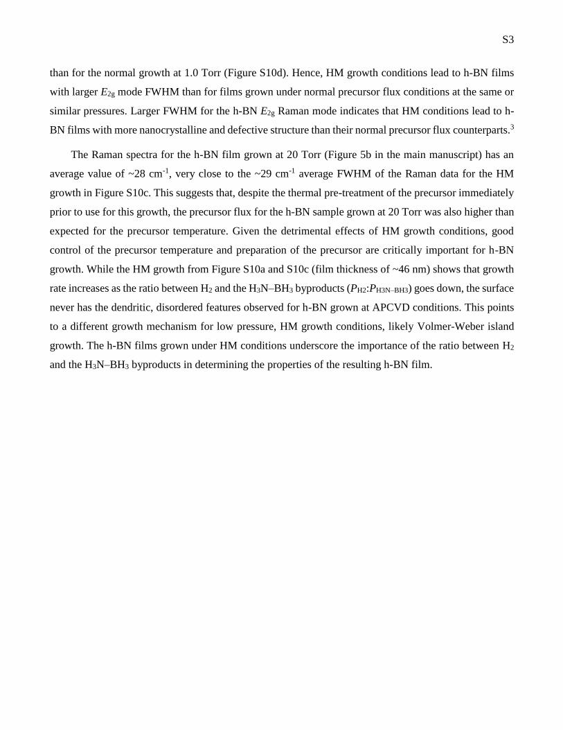
Figure S1. Experimental setup for CVD h-BN growth. (a) H3N–BH3 precursor cylinder and variac used to
modulate the ammonia borane sublimation temperature. (b) Polymerized H3N–BH3 breakdown products on a
stainless steel flange after CVD h-BN growth. For this run, the growth pressure was at 2.0 Torr, the growth time
was 25 min, and the precursor temperature was 95 °C. Polymerization occurs in the presence of high H3N–BH3
mass flow (high sublimation). Therefore, care must be taken to control the sublimation rate carefully.
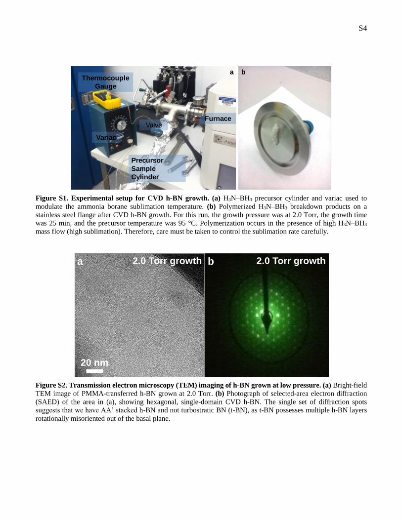
Figure S2. Transmission electron microscopy (TEM) imaging of h-BN grown at low pressure. (a) Bright-field
TEM image of PMMA-transferred h-BN grown at 2.0 Torr. (b) Photograph of selected-area electron diffraction
(SAED) of the area in (a), showing hexagonal, single-domain CVD h-BN. The single set of diffraction spots
suggests that we have AA’ stacked h-BN and not turbostratic BN (t-BN), as t-BN possesses multiple h-BN layers
rotationally misoriented out of the basal plane.
Precursor
Sample
Cylinder
Variac
ValveFurnace
Thermocouple
Gauge
a b
20 nm
a b2.0 Torr growth 2.0 Torr growth
S5
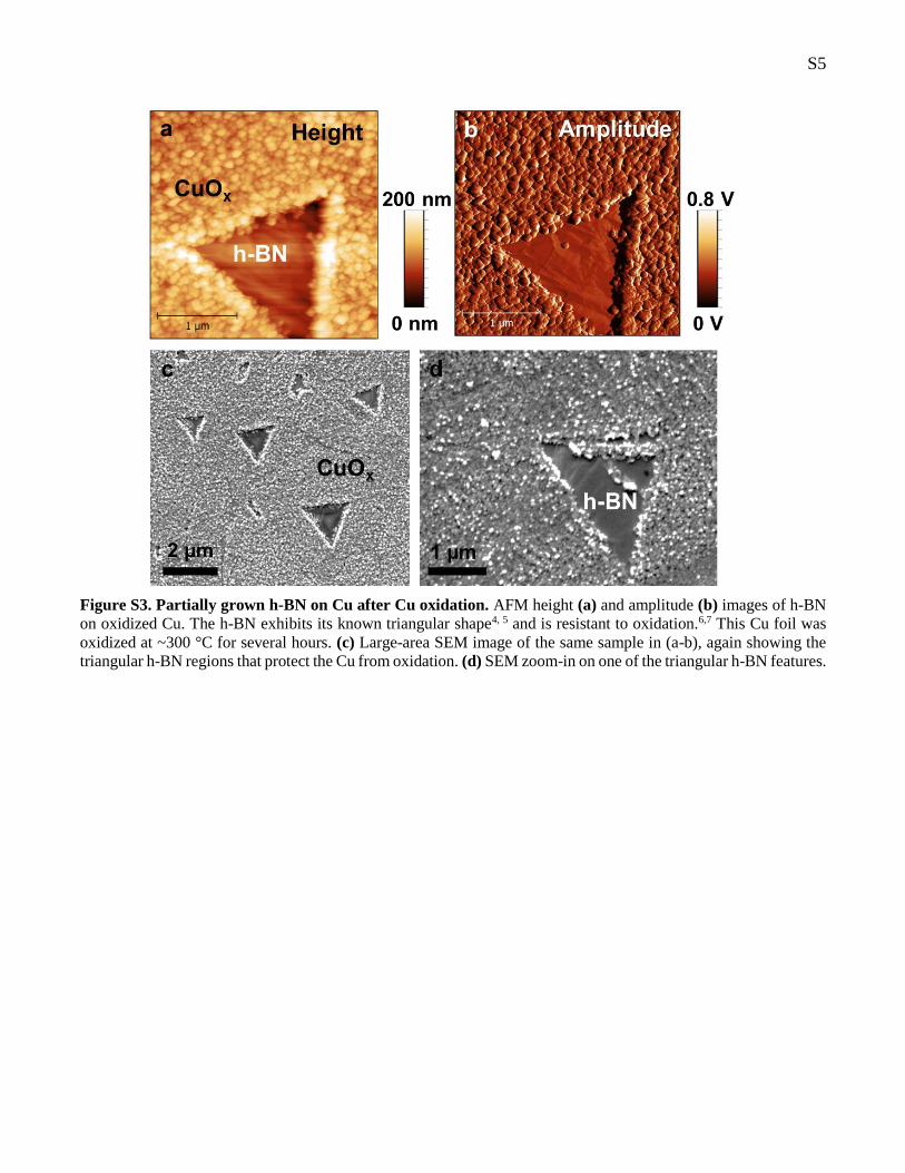
Figure S3. Partially grown h-BN on Cu after Cu oxidation. AFM height (a) and amplitude (b) images of h-BN
on oxidized Cu. The h-BN exhibits its known triangular shape4, 5 and is resistant to oxidation.6,7 This Cu foil was
oxidized at ~300 °C for several hours. (c) Large-area SEM image of the same sample in (a-b), again showing the
triangular h-BN regions that protect the Cu from oxidation. (d) SEM zoom-in on one of the triangular h-BN features.
S6
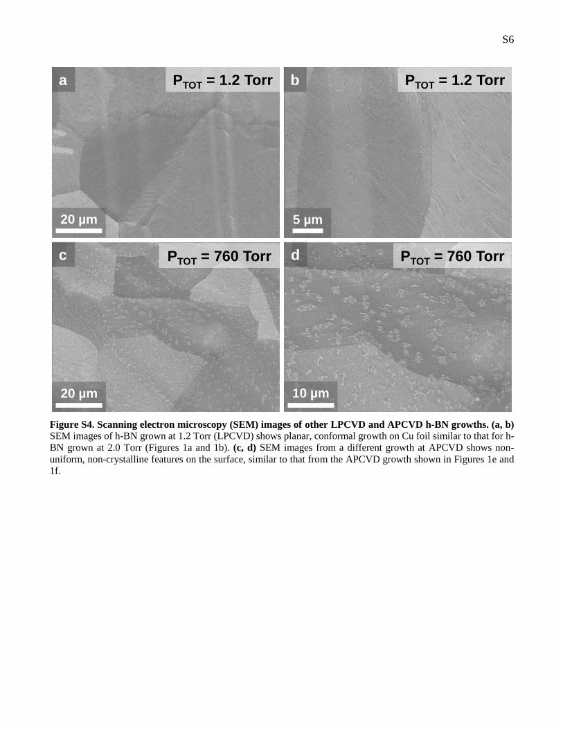
Figure S4. Scanning electron microscopy (SEM) images of other LPCVD and APCVD h-BN growths. (a, b) SEM images of h-BN grown at 1.2 Torr (LPCVD) shows planar, conformal growth on Cu foil similar to that for h-
BN grown at 2.0 Torr (Figures 1a and 1b). (c, d) SEM images from a different growth at APCVD shows non-
uniform, non-crystalline features on the surface, similar to that from the APCVD growth shown in Figures 1e and
1f.
20 µm
a PTOT = 1.2 Torr
5 µm
b PTOT = 1.2 Torr
20 µm
c PTOT = 760 Torr
10 µm
d PTOT = 760 Torr

S7
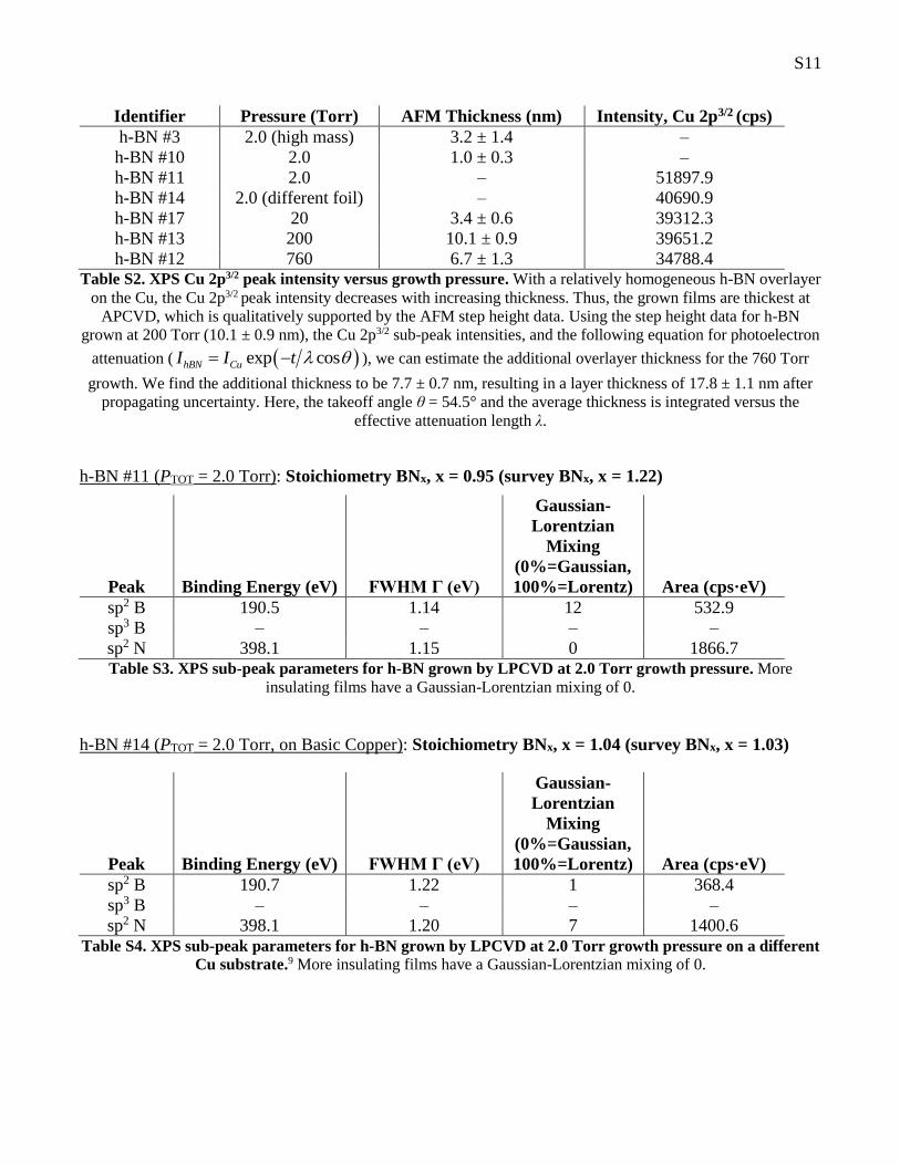
Figure S5. AFM height profiles for different h-BN growths. The step height contours indicate that the film
thickness, and thus growth rate, increases with growth pressure. The h-BN film grown at 760 Torr did not
completely etch, obscuring the actual film thickness.
Growth ID Growth Pressure
(Torr)
RMS Roughness (nm)
h-BN #46
h-BN #30
0.6 (HM)
1.2
9.60
0.58
h-BN #3
h-BN #10
2.0 (HM)
2.0
1.51
0.45
h-BN #17 20 3.20
h-BN #13 200 1.53
h-BN #12 760 1.64
Table S1. RMS roughness of h-BN versus growth pressure after transfer to SiO2/Si. AFM scans of h-BN after
transfer show that the roughness of the h-BN increases with growth pressure. While the roughness of the lowest
pressure growth (1.2 Torr) is higher than the 2.0 Torr growth, this is most likely due to the conformal nature of the
1 to 2 h-BN layer film on the substrate compared to the thicker film grown at 2.0 Torr. The standard error for each
measurement is shown.
0.0 0.5 1.0 1.5 2.00
2
4
0.0 0.2 0.4 0.6 0.8 1.00
2
4
0.0 0.5 1.0 1.5 2.0 2.50
5
10
15
0 1 2 3 40
5
10
15
0 1 2 30
5
10
15
0.0 0.5 1.0 1.5 2.00
2
42.0 Torr
h = 1.0 ± 0.3 nm
20 Torr
h = 3.4 ± 0.6 nm
He
igh
t (n
m)
Profile Distance (µm)
200 Torr, h = 10.1 ± 0.9 nm 760 Torr
h = 6.7 ± 1.3 nm
2.0 Torr, high mass flow
h = 3.2 ± 1.4 nm
1.2 Torr
h = 0.8 ± 0.1 nm
S8
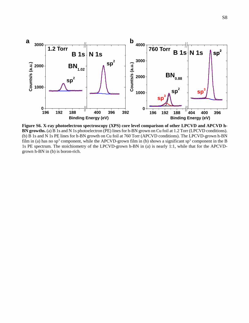
Figure S6. X-ray photoelectron spectroscopy (XPS) core level comparison of other LPCVD and APCVD h-
BN growths. (a) B 1s and N 1s photoelectron (PE) lines for h-BN grown on Cu foil at 1.2 Torr (LPCVD conditions).
(b) B 1s and N 1s PE lines for h-BN growth on Cu foil at 760 Torr (APCVD conditions). The LPCVD-grown h-BN
film in (a) has no sp3 component, while the APCVD-grown film in (b) shows a significant sp3 component in the B
1s PE spectrum. The stoichiometry of the LPCVD-grown h-BN in (a) is nearly 1:1, while that for the APCVD-
grown h-BN in (b) is boron-rich.
196 192 1880
1000
2000
3000
Co
un
ts/s
(a
.u.)
Binding Energy (eV)
400 396 392
BN1.02
B 1s N 1s
sp2
sp2
196 192 1880
1000
2000
3000
4000
sp3
N 1s
Co
un
ts/s
(a.u
.)
Binding Energy (eV)
B 1s
BN0.88
404 400 396
sp2
sp2
sp3
sp2
a b1.2 Torr 760 Torr
S9
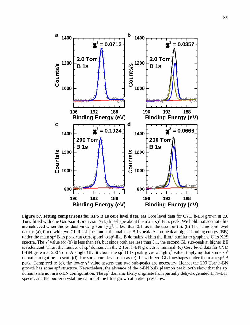
Figure S7. Fitting comparisons for XPS B 1s core level data. (a) Core level data for CVD h-BN grown at 2.0
Torr, fitted with one Gaussian-Lorentzian (GL) lineshape about the main sp2 B 1s peak. We hold that accurate fits
are achieved when the residual value, given by χ2, is less than 0.1, as is the case for (a). (b) The same core level
data as (a), fitted with two GL lineshapes under the main sp2 B 1s peak. A sub-peak at higher binding energy (BE)
under the main sp2 B 1s peak can correspond to sp3-like B domains within the film,8 similar to graphene C 1s XPS
spectra. The χ2 value for (b) is less than (a), but since both are less than 0.1, the second GL sub-peak at higher BE
is redundant. Thus, the number of sp3 domains in the 2 Torr h-BN growth is minimal. (c) Core level data for CVD
h-BN grown at 200 Torr. A single GL fit about the sp2 B 1s peak gives a high χ2 value, implying that some sp3
domains might be present. (d) The same core level data as (c), fit with two GL lineshapes under the main sp2 B
peak. Compared to (c), the lower χ2 value asserts that two sub-peaks are necessary. Hence, the 200 Torr h-BN
growth has some sp3 structure. Nevertheless, the absence of the c-BN bulk plasmon peak8 both show that the sp3
domains are not in a c-BN configuration. The sp3 domains likely originate from partially dehydrogenated H3N–BH3
species and the poorer crystalline nature of the films grown at higher pressures.
196 192 188
1000
1200
1400
196 192 188
1000
1200
1400
196 192 188
800
1000
1200
1400
196 192 188
800
1000
1200
1400
200 Torr
B 1s
200 Torr
B 1s
2.0 Torr
B 1s
2 = 0.0713
Co
un
ts/s
Binding Energy (eV)
2.0 Torr
B 1s
Co
un
ts/s
Binding Energy (eV)
2 = 0.0357
2 = 0.1924
Co
un
ts/s
Binding Energy (eV)
2 = 0.0666
Co
un
ts/s
Binding Energy (eV)
c d
a b
S10
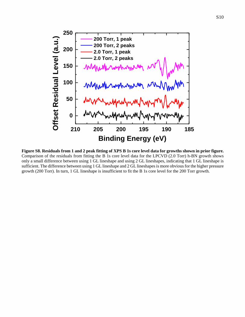
Figure S8. Residuals from 1 and 2 peak fitting of XPS B 1s core level data for growths shown in prior figure.
Comparison of the residuals from fitting the B 1s core level data for the LPCVD (2.0 Torr) h-BN growth shows
only a small difference between using 1 GL lineshape and using 2 GL lineshapes, indicating that 1 GL lineshape is
sufficient. The difference between using 1 GL lineshape and 2 GL lineshapes is more obvious for the higher pressure
growth (200 Torr). In turn, 1 GL lineshape is insufficient to fit the B 1s core level for the 200 Torr growth.
210 205 200 195 190 185
0
50
100
150
200
250
Off
se
t R
es
idu
al
Le
ve
l (a
.u.)
Binding Energy (eV)
200 Torr, 1 peak
200 Torr, 2 peaks
2.0 Torr, 1 peak
2.0 Torr, 2 peaks
S11
Identifier Pressure (Torr) AFM Thickness (nm) Intensity, Cu 2p3/2 (cps)
h-BN #3 2.0 (high mass) 3.2 ± 1.4 –
h-BN #10 2.0 1.0 ± 0.3 –
h-BN #11 2.0 – 51897.9
h-BN #14 2.0 (different foil) – 40690.9
h-BN #17 20 3.4 ± 0.6 39312.3
h-BN #13 200 10.1 ± 0.9 39651.2
h-BN #12 760 6.7 ± 1.3 34788.4 Table S2. XPS Cu 2p3/2 peak intensity versus growth pressure. With a relatively homogeneous h-BN overlayer
on the Cu, the Cu 2p3/2 peak intensity decreases with increasing thickness. Thus, the grown films are thickest at
APCVD, which is qualitatively supported by the AFM step height data. Using the step height data for h-BN
grown at 200 Torr (10.1 ± 0.9 nm), the Cu 2p3/2 sub-peak intensities, and the following equation for photoelectron
attenuation ( exp coshBN CuI I t ), we can estimate the additional overlayer thickness for the 760 Torr
growth. We find the additional thickness to be 7.7 ± 0.7 nm, resulting in a layer thickness of 17.8 ± 1.1 nm after
propagating uncertainty. Here, the takeoff angle θ = 54.5° and the average thickness is integrated versus the
effective attenuation length λ.
h-BN #11 (PTOT = 2.0 Torr): Stoichiometry BNx, x = 0.95 (survey BNx, x = 1.22)
Peak Binding Energy (eV) FWHM Γ (eV)
Gaussian-
Lorentzian
Mixing
(0%=Gaussian,
100%=Lorentz) Area (cps·eV)
sp2 B 190.5 1.14 12 532.9
sp3 B – – – –
sp2 N 398.1 1.15 0 1866.7 Table S3. XPS sub-peak parameters for h-BN grown by LPCVD at 2.0 Torr growth pressure. More
insulating films have a Gaussian-Lorentzian mixing of 0.
h-BN #14 (PTOT = 2.0 Torr, on Basic Copper): Stoichiometry BNx, x = 1.04 (survey BNx, x = 1.03)
Peak Binding Energy (eV) FWHM Γ (eV)
Gaussian-
Lorentzian
Mixing
(0%=Gaussian,
100%=Lorentz) Area (cps·eV)
sp2 B 190.7 1.22 1 368.4
sp3 B – – – –
sp2 N 398.1 1.20 7 1400.6
Table S4. XPS sub-peak parameters for h-BN grown by LPCVD at 2.0 Torr growth pressure on a different
Cu substrate.9 More insulating films have a Gaussian-Lorentzian mixing of 0.
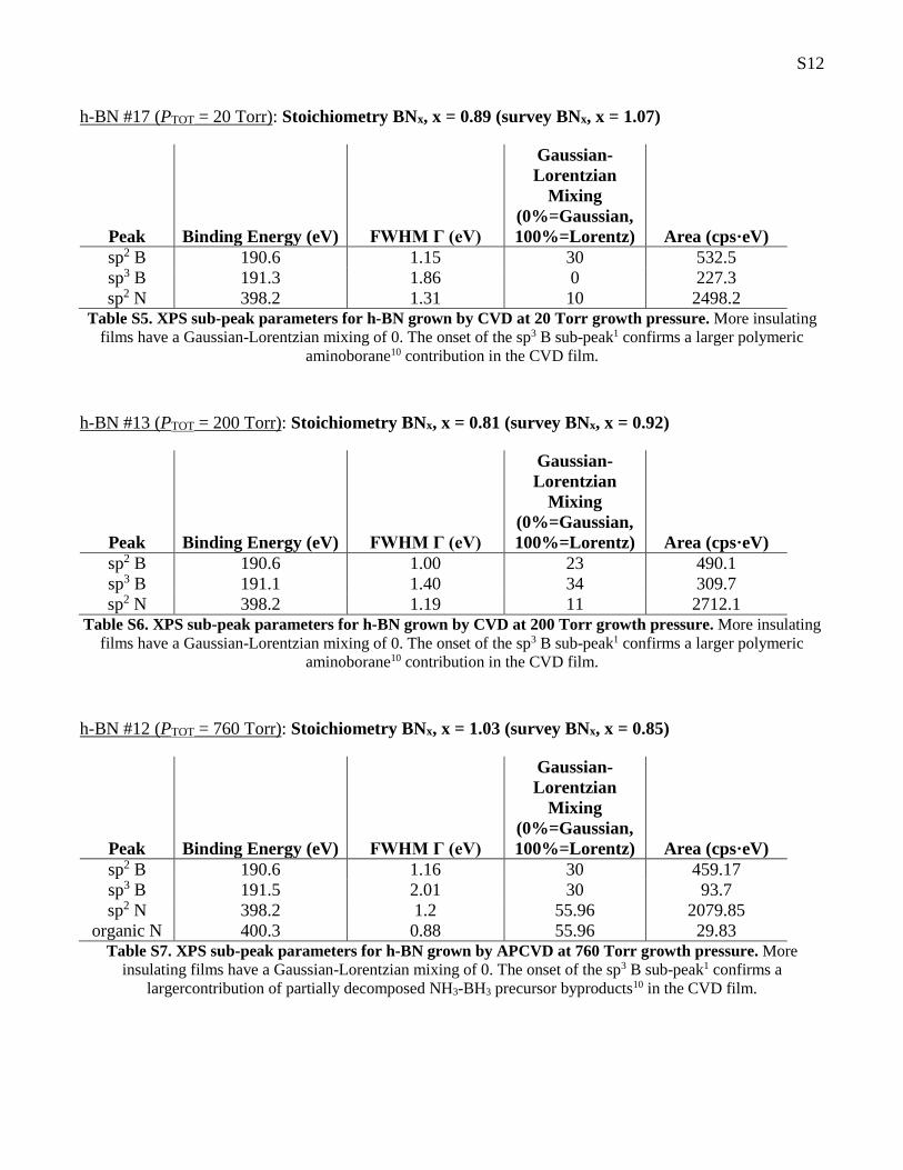
S12
h-BN #17 (PTOT = 20 Torr): Stoichiometry BNx, x = 0.89 (survey BNx, x = 1.07)
Peak Binding Energy (eV) FWHM Γ (eV)
Gaussian-
Lorentzian
Mixing
(0%=Gaussian,
100%=Lorentz) Area (cps·eV)
sp2 B 190.6 1.15 30 532.5
sp3 B 191.3 1.86 0 227.3
sp2 N 398.2 1.31 10 2498.2 Table S5. XPS sub-peak parameters for h-BN grown by CVD at 20 Torr growth pressure. More insulating
films have a Gaussian-Lorentzian mixing of 0. The onset of the sp3 B sub-peak1 confirms a larger polymeric
aminoborane10 contribution in the CVD film.
h-BN #13 (PTOT = 200 Torr): Stoichiometry BNx, x = 0.81 (survey BNx, x = 0.92)
Peak Binding Energy (eV) FWHM Γ (eV)
Gaussian-
Lorentzian
Mixing
(0%=Gaussian,
100%=Lorentz) Area (cps·eV)
sp2 B 190.6 1.00 23 490.1
sp3 B 191.1 1.40 34 309.7
sp2 N 398.2 1.19 11 2712.1 Table S6. XPS sub-peak parameters for h-BN grown by CVD at 200 Torr growth pressure. More insulating
films have a Gaussian-Lorentzian mixing of 0. The onset of the sp3 B sub-peak1 confirms a larger polymeric
aminoborane10 contribution in the CVD film.
h-BN #12 (PTOT = 760 Torr): Stoichiometry BNx, x = 1.03 (survey BNx, x = 0.85)
Peak Binding Energy (eV) FWHM Γ (eV)
Gaussian-
Lorentzian
Mixing
(0%=Gaussian,
100%=Lorentz) Area (cps·eV)
sp2 B 190.6 1.16 30 459.17
sp3 B 191.5 2.01 30 93.7
sp2 N
organic N
398.2
400.3
1.2
0.88
55.96
55.96
2079.85
29.83 Table S7. XPS sub-peak parameters for h-BN grown by APCVD at 760 Torr growth pressure. More
insulating films have a Gaussian-Lorentzian mixing of 0. The onset of the sp3 B sub-peak1 confirms a
largercontribution of partially decomposed NH3-BH3 precursor byproducts10 in the CVD film.
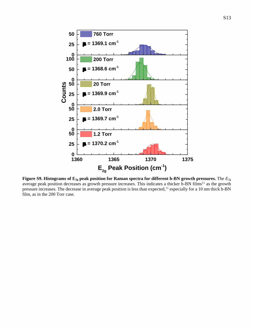
S13
Figure S9. Histograms of E2g peak position for Raman spectra for different h-BN growth pressures. The E2g
average peak position decreases as growth pressure increases. This indicates a thicker h-BN films11 as the growth
pressure increases. The decrease in average peak position is less than expected,11 especially for a 10 nm thick h-BN
film, as in the 200 Torr case.
0
25
50
= 1369.7 cm-1
2.0 Torr
0
50
100
= 1368.6 cm-1
200 Torr
0
25
50
= 1369.9 cm-1
Co
un
ts 20 Torr
1360 1365 1370 13750
25
50
= 1370.2 cm-1
E2g
Peak Position (cm-1)
1.2 Torr
0
25
50
= 1369.1 cm-1
760 Torr

S14
Figure S10. Raman histograms for h-BN grown with differing precursor amounts. Raman E2g band position
for LPCVD h-BN growth with high precursor flux condition (a) and LPCVD h-BN growth with normal precursor
flux condition (b). Due to a precursor problem during the growth in (a), there was a brief spike in the pressure when
opening the valve to the precursor ampoule from the 0.6 Torr background to 10 Torr. Such conditions greatly change
the ratio of precursor to H2 from normal growth process. Similar to the comparison between LPCVD and high
precursor flux LPCVD h-BN shown in Figure 5, the h-BN from (a) was thicker than that from (b), despite similar
growth pressures. Despite the different film thicknesses between the two growths, they share the same average E2g
band position at ~1371 cm-1. Comparing the full-width at half-maximum (FWHM) of the E2g Raman mode for the
two cases (c,d) shows that the high precursor flux LPCVD h-BN growth has a significantly higher FWHM compared
to the LPCVD growth with normal precursor flux. The larger FWHM value indicates that the high precursor flux
LPCVD h-BN growth is nanocrystalline,3 despite the low Ar/H2 background growth pressure used. Thus, the larger
ratios of precursor to Ar/H2 carrier gas create h-BN with smaller crystallite size. The h-BN film from (a, c) was
thick, with a step height of ~46 nm. This implies that in the high mass flow regime the surface catalysis reaction
rate is dominated by the mass transport reaction rate. Ultimately, the film’s thickness is determined by how much
H3N–BH3 can diffuse through a gas boundary layer. The high level of sensitivity for the h-BN growth reaction rates
is in striking contrast to graphene.12
1360 1365 1370 13750
25
50
75 = 1371 cm
-1
Co
un
ts
E2g
Peak Position (cm-1)
1.0 Torr
1360 1365 1370 13750
25
50
75
= 1371 cm-1
E2g
Peak Position (cm-1)
Co
un
ts0.6 Torr
High mass flow
0 10 20 30 400
25
50 = 20.5 cm
-1C
ou
nts
E2g
FWHM (cm-1)
1.0 Torr
0 10 20 30 400
25
50 = 29.2 cm-1
Co
un
ts
E2g
FWHM (cm-1)
0.6 Torr
High mass flow
dc
a b
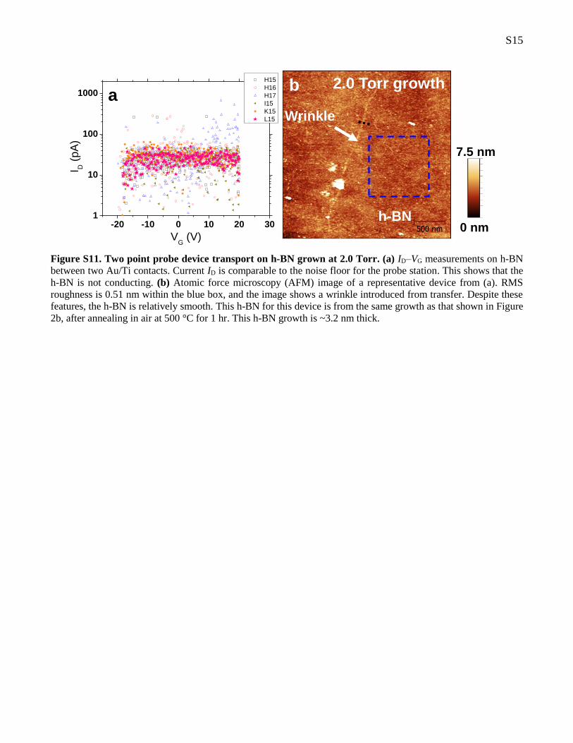
S15
Figure S11. Two point probe device transport on h-BN grown at 2.0 Torr. (a) ID–VG measurements on h-BN
between two Au/Ti contacts. Current ID is comparable to the noise floor for the probe station. This shows that the
h-BN is not conducting. (b) Atomic force microscopy (AFM) image of a representative device from (a). RMS
roughness is 0.51 nm within the blue box, and the image shows a wrinkle introduced from transfer. Despite these
features, the h-BN is relatively smooth. This h-BN for this device is from the same growth as that shown in Figure
2b, after annealing in air at 500 °C for 1 hr. This h-BN growth is ~3.2 nm thick.
-20 -10 0 10 20 301
10
100
1000
I D
(pA
)
VG (V)
H15
H16
H17
I15
K15
L15
h-BN
Wrinkle
2.0 Torr growth
7.5 nm
0 nm
ab
S16
References
1. Vlassiouk, I.; Regmi, M.; Fulvio, P.; Dai, S.; Datskos, P.; Eres, G.; Smirnov, S. Role of Hydrogen in
Chemical Vapor Deposition Growth of Large Single-Crystal Graphene. ACS Nano 2011, 5 (7), 6069-
6076.
2. Zhang, W.; Wu, P.; Li, Z.; Yang, J. First-Principles Thermodynamics of Graphene Growth on Cu
Surfaces. J. Phys. Chem. C 2011, 115 (36), 17782-17787.
3. Nemanich, R. J.; Solin, S. A.; Martin, R. M. Light Scattering Study of Boron Nitride Microcrystals.
Phys. Rev. B 1981, 23 (12), 6348-6356.
4. Auwärter, W.; Suter, H. U.; Sachdev, H.; Greber, T. Synthesis of One Monolayer of Hexagonal Boron
Nitride on Ni(111) from B-Trichloroborazine (ClBNH)3. Chem. Mater. 2004, 16 (2), 343-345.
5. Kim, K. K.; Hsu, A.; Jia, X.; Kim, S. M.; Shi, Y.; Hofmann, M.; Nezich, D.; Rodriguez-Nieva, J.;
Dresselhaus, M.; Palacios, T.; Kong, J. Synthesis of Monolayer Hexagonal Boron Nitride on Cu Foil
using Chemical Vapor Deposition. Nano Lett. 2012, 12 (1), 161-166.
6. Li, L. H.; Cervenka, J.; Watanabe, K.; Taniguchi, T.; Chen, Y. Strong Oxidation Resistance of
Atomically Thin Boron Nitride Nanosheets. ACS Nano 2014, 8 (2), 1457-1462.
7. Liu, Z.; Gong, Y.; Zhou, W.; Ma, L.; Yu, J.; Idrobo, J. C.; Jung, J.; MacDonald, A. H.; Vajtai, R.; Lou,
J.; Ajayan, P. M. Ultrathin High-Temperature Oxidation-Resistant Coatings of Hexagonal Boron
Nitride. Nat. Commun. 2013, 4, 2541.
8. Panayiotatos, Y.; Logothetidis, S.; Handrea, M.; Kautek, W. Homogeneous and amorphous sputtered
sp3-bonded BN films at RT: a stress, spectroscopic ellipsometry and XPS study. Diam. Relat. Mater.
2003, 12 (3–7), 1151-1156.
9. Wood, J. D.; Schmucker, S. W.; Lyons, A. S.; Pop, E.; Lyding, J. W. Effects of Polycrystalline Cu
Substrate on Graphene Growth by Chemical Vapor Deposition. Nano Lett. 2011, 11 (11), 4547-4554.
10. Frueh, S.; Kellett, R.; Mallery, C.; Molter, T.; Willis, W. S.; King'ondu, C.; Suib, S. L. Pyrolytic
Decomposition of Ammonia Borane to Boron Nitride. Inorg. Chem. 2011, 50 (3), 783-792.
11. Gorbachev, R. V.; Riaz, I.; Nair, R. R.; Jalil, R.; Britnell, L.; Belle, B. D.; Hill, E. W.; Novoselov, K.
S.; Watanabe, K.; Taniguchi, T.; Geim, A. K.; Blake, P. Hunting for Monolayer Boron Nitride: Optical
and Raman Signatures. Small 2011, 7 (4), 465-468.
12. Bhaviripudi, S.; Jia, X.; Dresselhaus, M. S.; Kong, J. Role of Kinetic Factors in Chemical Vapor
Deposition Synthesis of Uniform Large Area Graphene using Copper Catalyst. Nano Lett. 2010, 10
(10), 4128-4133.