![TME-DC [ ] - Sew Many Parts, Inc. of Contents z TME-DC GENERAL VIEW z TME-DC FRAME … CD-1 z TME-DC TABLE … CD-2-1 z TME-DC AUTO SUB TABLE …](https://static.fdocuments.net/doc/165x107/5b1d28797f8b9add7f8b64eb/tme-dc-sew-many-parts-inc-of-contents-z-tme-dc-general-view-z-tme-dc-frame.jpg)
RoHS 2002/95/EC - TME
22
VACUUM FLUORESCENT DISPLAY MODULE SPECIFICATION MODEL : CU20049-UW2A SPECIFICATION NO. : DS-1401-0000-05 DATE OF ISSUE : April 5, 2007 (00R) REVISION : July 17, 2007 (00) : December 5, 2007 (01) : January 7, 2008 (02) : June 27, 2008 (03) : July 22, 2009 (04) : September 21, 2010 (05) PUBLISHED BY NORITAKE ITRON CORP. / JAPAN http://www.noritake-itron.jp This specification is subject to change without prior notice. RoHS 2002/95/EC This product complies with RoHS Directive 2002/95/EC
Transcript of RoHS 2002/95/EC - TME
VACUUM FLUORESCENT DISPLAY
MODULE
SPECIFICATION
MODEL : CU20049-UW2A
SPECIFICATION NO. : DS-1401-0000-05
D A T E O F I S S U E : April 5, 2007 (00R)
R E V I S I O N : July 17, 2007 (00)
: December 5, 2007 (01)
: January 7, 2008 (02)
: June 27, 2008 (03)
: July 22, 2009 (04)
: September 21, 2010 (05)
PUBLISHED BY
NORITAKE ITRON CORP. / JAPAN
http://www.noritake-itron.jp
This specification is subject to change without prior notice.
RoHS 2002/95/EC
This product complies with RoHS Directive 2002/95/EC
CU20049-UW2A
1
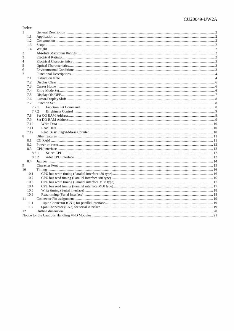
Index 1 General Description ...................................................................................................................................................................... 2
1.1 Application ................................................................................................................................................................................... 2 1.2 Construction ................................................................................................................................................................................. 2 1.3 Scope ............................................................................................................................................................................................ 2 1.4 Weight .......................................................................................................................................................................................... 2
2 Absolute Maximum Ratings ......................................................................................................................................................... 2 3 Electrical Ratings .......................................................................................................................................................................... 2 4 Electrical Characteristics .............................................................................................................................................................. 3 5 Optical Characteristics .................................................................................................................................................................. 3 6 Environmental Conditions ............................................................................................................................................................ 3 7 Functional Descriptions ................................................................................................................................................................ 4
7.1 Instruction table ............................................................................................................................................................................ 4 7.2 Display Clear ................................................................................................................................................................................ 6 7.3 Cursor Home ................................................................................................................................................................................ 6 7.4 Entry Mode Set ............................................................................................................................................................................. 6 7.5 Display ON/OFF ........................................................................................................................................................................... 7 7.6 Cursor/Display Shift ..................................................................................................................................................................... 8 7.7 Function Set .................................................................................................................................................................................. 8
7.7.1 Function Set Command ...................................................................................................................................................... 8 7.7.2 Brightness Control ............................................................................................................................................................. 9
7.8 Set CG RAM Address................................................................................................................................................................... 9 7.9 Set DD RAM Address .................................................................................................................................................................. 9 7.10 Write Data ............................................................................................................................................................................. 10 7.11 Read Data .............................................................................................................................................................................. 10 7.12 Read Busy Flag/Address Counter .......................................................................................................................................... 10
8 Other features ............................................................................................................................................................................. 11 8.1 CG RAM .................................................................................................................................................................................... 11 8.2 Power-on reset ............................................................................................................................................................................ 12 8.3 CPU interface ............................................................................................................................................................................. 12
8.3.1 Select CPU ....................................................................................................................................................................... 12 8.3.2 4-bit CPU interface .......................................................................................................................................................... 12
8.4 Jumper ........................................................................................................................................................................................ 14 9 Character Font ............................................................................................................................................................................ 15 10 Timing ........................................................................................................................................................................................ 16
10.1 CPU bus write timing (Parallel interface i80 type) ................................................................................................................ 16 10.2 CPU bus read timing (Parallel interface i80 type) ................................................................................................................. 16 10.3 CPU bus write timing (Parallel interface M68 type) ............................................................................................................. 17 10.4 CPU bus read timing (Parallel interface M68 type)............................................................................................................... 17 10.5 Write timing (Serial interface) ............................................................................................................................................... 18 10.6 Read timing (Serial interface) ................................................................................................................................................ 18
11 Connector Pin assignment .......................................................................................................................................................... 19 11.1 14pin Connector (CN1) for parallel interface ........................................................................................................................ 19 11.2 6pin Connector (CN3) for serial interface ............................................................................................................................. 19
12 Outline dimension ...................................................................................................................................................................... 20 Notice for the Cautious Handling VFD Modules ....................................................................................................................................... 21

CU20049-UW2A
2
1 General Description
1.1 Application : Readout of computer, micro-computer, communication terminal and automatic
instruments.
1.2 Construction : Single board display module consists of 80 characters (4×20) VFD, a
controller which includes character generator ROM, RAM and DC/DC
converter.
1.3 Scope : Interface is 8/4 bit parallel and synchronous serial.
+5V single power supply is required.
1.4 Weight : About 155 g
2 Absolute Maximum Ratings
Parameter Symbol Min. Typ. Max. Unit Condition
Power Supply Voltage VCC 0 – 5.5 VDC –
Logic Input Voltage VI 0 – VCC+0.3 VDC –
3 Electrical Ratings
Measuring Conditions: TA (Ambient temperature) = 25 degree
Parameter Symbol Min. Typ. Max. Unit Condition
Logic Input Voltage DB0-DB7, RS,
R/W(WR), E(RD),
SCK, STB
"H" VIH1 2.0 – VCC VDC
VCC - VSS
= 5.0V "L" VIL1 VSS – 0.8
Logic Input Voltage SI/SO
"H" VIH2 0.7VCC – VCC VDC
VCC - VSS
= 5.0V "L" VIL2 VSS – 0.3VCC
Logic Input Voltage /RESET
"H" VIH3 0.8VCC – VCC VDC
VCC – VSS
= 5.0V "L" VIL3 VSS – 0.2VCC
Power supply Voltage VCC-VSS 4.75 5.00 5.25 VDC –
Note: "/RESET" must be driven by open-collector or open-drain because this module has an
internal Reset-IC.
VCC
C
R 10K
Controller
Reset IC
out
/RESET
Configuration of Reset-IC peripheral circuit.
CU20049-UW2A
3
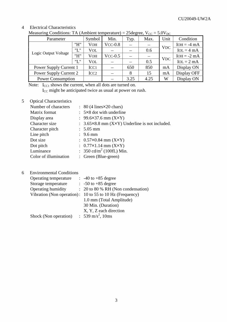
4 Electrical Characteristics
Measuring Conditions: TA (Ambient temperature) = 25degree, VCC = 5.0VDC
Parameter Symbol Min. Typ. Max. Unit Condition
Logic Output Voltage
"H" VOH VCC-0.8 – – VDC
IOH = -4 mA
"L" VOL – – 0.6 IOL = 4 mA
"H" VOH VCC-0.5 – – VDC
IOH = -2 mA
"L" VOL – – 0.5 IOL = 2 mA
Power Supply Current 1 ICC1 – 650 850 mA Display ON
Power Supply Current 2 ICC2 – 8 15 mA Display OFF
Power Consumption – 3.25 4.25 W Display ON
Note: ICC1 shows the current, when all dots are turned on.
ICC might be anticipated twice as usual at power on rush.
5 Optical Characteristics
Number of characters : 80 (4 lines×20 chars)
Matrix format : 5×8 dot with underline
Display area : 99.6×37.6 mm (X×Y)
Character size : 3.65×8.8 mm (X×Y) Underline is not included.
Character pitch : 5.05 mm
Line pitch : 9.6 mm
Dot size : 0.57×0.84 mm (X×Y)
Dot pitch : 0.77×1.14 mm (X×Y)
Luminance : 350 cd/m2 (100fL) Min.
Color of illumination : Green (Blue-green)
6 Environmental Conditions
Operating temperature : -40 to +85 degree
Storage temperature : -50 to +85 degree
Operating humidity : 20 to 80 % RH (Non condensation)
Vibration (Non operation) : 10 to 55 to 10 Hz (Frequency)
1.0 mm (Total Amplitude)
30 Min. (Duration)
X, Y, Z each direction
Shock (Non operation) : 539 m/s2, 10ms

CU20049-UW2A
4
7 Functional Descriptions
7.1 Instruction table
Instruction CODE
Time Description RS R/W DB7 DB6 DB5 DB4 DB3 DB2 DB1 DB0
Display
Clear 0 0 0 0 0 0 0 0 0 1
100μs
MAX.
Clears all display
and sets DD RAM
address 0 in the
address counter.
Cursor
Home 0 0 0 0 0 0 0 0 1 * 666ns
Sets DD RAM
address 0 in the
address counter.
Also returns the
display being
shifted to the
original position.
DD RAM contents
remain unchanged.
Entry
Mode Set 0 0 0 0 0 0 0 1 I/D S 666ns
Sets the cursor
direction and
specifies display
shift. These
operations are
performed during
writing/reading
data.
Display
ON/OFF
Control
0 0 0 0 0 0 1 D C B 666ns
Sets all display
ON/OFF(D),
cursor
ON/OFF(C),
cursor blink of
character position
(B).
Cursor or
Display
Shift
0 0 0 0 0 1 S/C R/L * * 666ns
Shifts display or
cursor, keeping
DD RAM
contents.
Function
Set 0 0 0 0 1 IF * * * * 666ns
Sets data length
(IF).
Brightness
Control 1 0 * * * * * * BR1 BR0 666ns
Accepts 1 byte
data of just after
"Function set" as
brightness control
data.

CU20049-UW2A
5
Instruction CODE
Time Description RS R/W DB7 DB6 DB5 DB4 DB3 DB2 DB1 DB0
CG RAM
Address
setting
0 0 0 1 ACG 666ns
Sets the CG RAM
address.
DD RAM
Address
setting
0 0 1 ADD 666ns
Sets the DD RAM
address.
Busy flag
& Address
Reading
0 1 BF ACC 666ns
Reads busy flag
(BF) and address
counter.
Data
Writing to
CG or DD
RAM
1 0 Data writing 666ns
Writes data into
CG RAM or DD
RAM.
Data
Reading
from CG or
DD RAM
1 1 Data reading 666ns
Reads data from
CG RAM or DD
RAM.
I/D = 1 : Increment
I/D = 0 : Decrement
S = 1 : Display shift enabled
S = 0 : Cursor shift enabled
S/C = 1 : Display shift
S/C = 0 : Cursor move
R/L = 1 : Shift to the right
R/L = 0 : Shift to the left
BR1,BR0 = 00 : 100%
01 : 75%
10 : 50%
11 : 25%
IF = 1 : 8-bits
IF = 0 : 4-bits
BF = 1 : Busy
BF = 0 : Not busy
DD RAM:
Display Data
RAM
CG RAM:
Character
Generator RAM
ACG:
CG RAM Address
ADD:
DD RAM Address
ACC:
Address Counter
Note:
*: Don't care.

CU20049-UW2A
6
7.2 Display Clear
DB7 DB6 DB5 DB4 DB3 DB2 DB1 DB0
0 0 0 0 0 0 0 1 01H
RS=0
This instruction
1. Fills all locations in the display data (DD) RAM with 20H (Blank character).
2. Clears the contents of the address counter to 0H.
3. Sets the display for zero character shift.
4. Sets the address counter to point to the DD RAM.
5. If the cursor is displayed, the cursor moves to the left most character in the top line (Line 1).
6. Sets the address counter to increment on each access of DD RAM or CG RAM.
7.3 Cursor Home
DB7 DB6 DB5 DB4 DB3 DB2 DB1 DB0
0 0 0 0 0 0 1 * 02H to 03H
RS=0
*: Don't care.
This instruction
1. Clears the contents of the address counter to 0H.
2. Sets the address counter to point to the DD RAM.
3. Sets the display for zero character shift.
4. If the cursor is displayed, moves the left most character in the top line. (Line 1).
7.4 Entry Mode Set
DB7 DB6 DB5 DB4 DB3 DB2 DB1 DB0
0 0 0 0 0 1 I/D S 04H to 07H
RS=0
The I/D bit selects the way in which the contents of the address counter are modified after every
access to DD RAM or CG RAM.
I/D=1: The address counter is increment.
I/D=0: The address counter is decrement.
The S bit enables display shifts instead of cursor shift, after each write or read to the DD RAM.
S=1: Display shift enabled.
S=0: Cursor shift enabled.
The direction in which the display is shifted is opposite in sense to that of the cursor. For example
if S=0 and I/D=1, the cursor would shift one character to the right after a CPU writes to DD RAM.
However if S=1 and I/D=1, the display would shift one character to the left and the cursor would
maintain its position on the panel.

CU20049-UW2A
7
The cursor will already be shifted in the direction selected by I/D during reads of the DD RAM,
irrespective of the value of S. Similarly reading and writing the CG RAM always shifts the cursor.
Also both lines are shifted simultaneously.
Cursor move and Display shift by the "Entry Mode Set"
I/D S After writing DD RAM data After reading DD RAM data
0 0 The cursor moves one character to
the left.
The cursor moves one character to
the left.
1 0 The cursor moves one character to
the right.
The cursor moves one character to
the right.
0 1 The display shifts one character to the
right without cursor's move.
The cursor moves one character to
the left.
1 1 The display shifts one character to the
left without cursor's move.
The cursor moves one character to
the right.
7.5 Display ON/OFF
DB7 DB6 DB5 DB4 DB3 DB2 DB1 DB0
0 0 0 0 1 D C B 08H to 0FH
RS=0
This instruction controls various features of the display.
The D bit turns the entire display on or off.
D=1: Display on
D=0: Display off
Note: When display is turned off, power converter is also inhibited and reduces power
consumption.
The C bit turns the cursor on or off.
C=1: Cursor on
C=0: Cursor off
The B bit enables blinking of the character the cursor coincides with.
B=1: Blinking on
B=0: Blinking off
Blinking is achieved by alternating between a normal and all on display of a character.
The cursor blinks with a frequency of about 1Hz and DUTY 50%.

CU20049-UW2A
8
7.6 Cursor/Display Shift
DB7 DB6 DB5 DB4 DB3 DB2 DB1 DB0
0 0 0 1 S/C R/L * * 10H to 1FH
RS=0
*: Don't care.
This instruction shifts the display and/or moves the cursor, on character to either left or right,
without neither reading nor writing DD RAM.
The S/C bit selects movement of the cursor or movement of both the cursor and the display.
S/C=1: Shift both cursor and display.
S/C=0: Shift cursor only.
The R/L bit selects left ward or right ward movement of the display and/or cursor.
R/L=1: Shift one character right.
R/L=0: Shift one character left.
Cursor move and Display shift by the "Cursor/Display Shift"
S/C R/L Cursor shift Display shift
0 0 Move one character to the left No shift
0 1 Move one character to the right No shift
1 0 Shift one character to left with display Shift one character to the left
1 1 Shift one character to right with display Shift one character to the right
7.7 Function Set
This command sets width of data bus line by itself, and sets screen brightness by following one
byte data.
7.7.1 Function Set Command
DB7 DB6 DB5 DB4 DB3 DB2 DB1 DB0
0 0 1 IF * * * * 20H to 3FH
RS=0
*: Don't care.
This instruction initializes the system, and must be the first instruction executed after power-on.
The IF bit selects between an 8-bit or a 4-bit bus width interface.
IF=1: 8-bit CPU interface using DB7 to DB0
IF=0: 4-bit CPU interface using DB7 to DB4
When serial interface is selected, IF=1.

CU20049-UW2A
9
7.7.2 Brightness Control
DB7 DB6 DB5 DB4 DB3 DB2 DB1 DB0
* * * * * * BR1 BR0 00H to 03H
RS=1
*: Don't care.
One byte data (RS=1) which follows the "Function Set Command" is considered as brightness data.
When a command (RS=0) is written after the "Function Set Command", the brightness control
function is not initiated. Screen brightness is as follows.
BR1 BR0 Brightness
0 0 100 % (Default)
0 1 75 %
1 0 50 %
1 1 25 %
7.8 Set CG RAM Address
DB7 DB6 DB5 DB4 DB3 DB2 DB1 DB0
0 1 ACG 40H to 7FH
RS=0
This instruction
1. Loads a new 6-bit address into the address counter.
2. Sets the address counter to address CG RAM.
Once "Set CG RAM Address" has been executed, the contents of the address counter will be
automatically modified after every access of CG RAM, as determined by the "7.4 Entry Mode Set"
instruction. The active width of the address counter, when it is addressing CG RAM, is 6-bits so
the counter will wrap around to 00H from 3FH if more than 64 bytes of data are written to CG
RAM.
7.9 Set DD RAM Address
DB7 DB6 DB5 DB4 DB3 DB2 DB1 DB0
1 ADD
RS=0
80H to 93H (1 line), C0H to D3H (2 line), 94H to A7H (3 line), D4H to E7H (4 line)
This instruction
1. Loads a new 7-bit address into the address counter.
2. Sets the address counter to point to the DD RAM.
Once the "Set DD RAM Address" instruction has been executed, the contents of the address
counter will be automatically modified after each access of DD RAM, as selected by the "7.4 Entry
Mode Set" instruction.

CU20049-UW2A
10
Valid DD RAM Address (ADD) Range
Number of Characters Address
1st line 20 00H to 13H
2nd line 20 40H to 53H
3rd line 20 14H to 27H
4th line 20 54H to 67H
7.10 Write Data
DB7 DB6 DB5 DB4 DB3 DB2 DB1 DB0
DATA WRITE 00H to FFH
RS=1
This instruction writes the data in DB7 to DB0 into either the CG RAM or the DD RAM.
The RAM space (CG or DD), and the address in that space, that is accessed depends on whether a
"Set CG RAM Address" or "Set DD RAM Address" instruction was last executed, and on the
parameters of that instruction. The contents of the address counter will be automatically modified
after each "Write Data", as determined by the "7.4 Entry Mode Set". When data is written to the
CG RAM, the DB7, DB6 and DB5 bits are not displayed as characters.
7.11 Read Data
DB7 DB6 DB5 DB4 DB3 DB2 DB1 DB0
DATA READ
RS=1
This instruction reads data from either CG RAM or DD RAM, depending on the type of "Set RAM
Address" instructions last sent. The address in that space depends on the "Set RAM Address"
instruction parameters. Immediately before executing "Read Data", "Set CG RAM Address" or
"Set DD RAM Address" must be executed. The contents of the address counter are modified after
each "Read Data". As determined by the "7.4 Entry Mode Set". Display shift is not executed, as
described at of the "7.4 Entry Mode Set".
7.12 Read Busy Flag/Address Counter
DB7 DB6 DB5 DB4 DB3 DB2 DB1 DB0
BF ACC
RS=0
Reading the instruction register yields the current value of the address counter and the busy flag.
This instruction must be executed prior to any other instructions. ACC, the address counter value,
will point to a location in either CG RAM or DD RAM, depending on the type of "Set RAM
Address" instruction last sent.
In "Busy Flag Check" immediately after executing "Write Data" instruction, a valid address
counter value can be ready as soon as BF goes low. The BF bit shows the status of the busy flag.
BF=1: busy.
BF=0: ready for next instruction, command receivable.
CU20049-UW2A
11
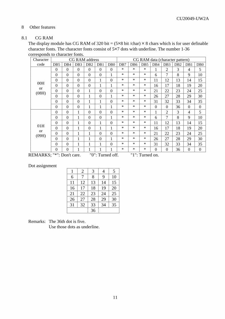
8 Other features
8.1 CG RAM
The display module has CG RAM of 320 bit = (5×8 bit /char) × 8 chars which is for user definable
character fonts. The character fonts consist of 5×7 dots with underline. The number 1-36
corresponds to character fonts. Character
code
CG RAM address CG RAM data (character pattern) DB5 DB4 DB3 DB2 DB1 DB0 DB7 DB6 DB5 DB4 DB3 DB2 DB1 DB0
00H
or
(08H)
0 0 0 0 0 0 * * * 1 2 3 4 5
0 0 0 0 0 1 * * * 6 7 8 9 10
0 0 0 0 1 0 * * * 11 12 13 14 15
0 0 0 0 1 1 * * * 16 17 18 19 20
0 0 0 1 0 0 * * * 21 22 23 24 25
0 0 0 1 0 1 * * * 26 27 28 29 30
0 0 0 1 1 0 * * * 31 32 33 34 35
0 0 0 1 1 1 * * * 0 0 36 0 0
01H
or
(09H)
0 0 1 0 0 0 * * * 1 2 3 4 5
0 0 1 0 0 1 * * * 6 7 8 9 10
0 0 1 0 1 0 * * * 11 12 13 14 15
0 0 1 0 1 1 * * * 16 17 18 19 20
0 0 1 1 0 0 * * * 21 22 23 24 25
0 0 1 1 0 1 * * * 26 27 28 29 30
0 0 1 1 1 0 * * * 31 32 33 34 35
0 0 1 1 1 1 * * * 0 0 36 0 0
REMARKS; "*": Don't care. "0": Turned off. "1": Turned on.
Dot assignment
1 2 3 4 5
6 7 8 9 10
11 12 13 14 15
16 17 18 19 20
21 22 23 24 25
26 27 28 29 30
31 32 33 34 35
36
Remarks: The 36th dot is five.
Use those dots as underline.

CU20049-UW2A
12
8.2 Power-on reset
Internal status of the module is initialized, when the controller detects the rising of power supply
up. The statuses are as follows:
1. Display clear
Fills the DD RAM with 20Hex (Space code).
During executing of "Display Clear" (Max. 100μs), the busy flag (BF) is "1".
2. Sets the address counter to 0H.
Sets the address counter to point the DD RAM.
3. Display ON/OFF
D=0: Display OFF
C=0: Cursor OFF
B=0: Blink OFF
4. Entry Mode Set
I/D=1: Increment (+1)
S=0: No display shift
5. Function Set
IF=1: 8-bit interface
6. Brightness Control
BR0=BR1=0: 100%
Remarks
There is a possibility that reset doesn't work by slow start power supply.
Therefore the initializing by commands needs.
8.3 CPU interface
The display module is capable to select some interfaces such as parallel (i80 or M68, 8-bit or 4-bit)
or serial.
8.3.1 Select CPU
The module is able to select to parallel or serial data transfer by setting JP7 jumper, and to connect
to bus of i80 type or M68 type CPU by setting JP2 jumper. Refer to "8.4 Jumper" for detail.
8.3.2 4-bit CPU interface
If 4-bit interface is used, the 8-bit instruction is written nibble by nibble: the high-order nibble
being written first, followed by low-order nibble. It is not necessary to check the busy flag between
writing separate nibbles of individual instructions.
Refer to "7.7.1 Function Set Command" for detail.
CU20049-UW2A
13
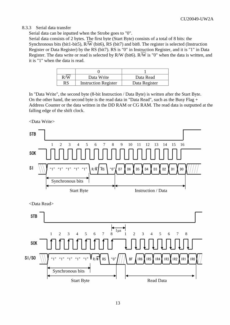
8.3.3 Serial data transfer
Serial data can be inputted when the Strobe goes to "0".
Serial data consists of 2 bytes. The first byte (Start Byte) consists of a total of 8 bits: the
Synchronous bits (bit1-bit5), R/W (bit6), RS (bit7) and bit8. The register is selected (Instruction
Register or Data Register) by the RS (bit7). RS is "0" in Instruction Register, and it is "1" in Data
Register. The data write or read is selected by R/W (bit6). R/W is "0" when the data is written, and
it is "1" when the data is read.
0 1
R/W Data Write Data Read
RS Instruction Register Data Register
In "Data Write", the second byte (8-bit Instruction / Data Byte) is written after the Start Byte.
On the other hand, the second byte is the read data in "Data Read", such as the Busy Flag +
Address Counter or the data written in the DD RAM or CG RAM. The read data is outputted at the
falling edge of the shift clock.
<Data Write>
<Data Read>
IR0 IR3 IR5 IR6 IR4 IR1 IR2
1 2 3 4 5 6 7 8 1 2 3 4 5 6 7 8
SI/SO
STB
BF
SCK
RS R/W “0” “1” “1” “1” “1” “1”
Synchronous bits
Start Byte Read Data
1μs
STB
Synchronous bits
Start Byte Instruction / Data
R/W D0 D1 D2 D3
M
in.
60
ns
D4 D5 D7 D6 RS “0” “1” “1” “1” “1” “1” SI
1 2 3 4 5 6 7 8 9 10 11 12 13 14 15 16
SCK

CU20049-UW2A
14
8.4 Jumper
Some jumpers are prepared on the PCB board, to set operating mode of the display module.
A soldering iron is required to short jumper.
No.2 and No.3 of jumper 'JP4' are used to reset of module.
You can reset the module by shorting No.2 and No.3 of the jumper 'JP4' for some interval which is
longer than 10us.
The following figure shows the location of each jumper.
Location
J P 1
J P 2
J P 4
JP5
IC4
J P 6
J P 7
J P 8
J P 9
The following table shows the function of No.1 and No.2 of JP4, JP2 and JP7.
Default setting is no external reset inputs and M68 CPU bus parallel interface.
External reset input signal is active when it is low.
Table of No 1 and No 2 of JP4 setting
No.1 and No.2 of JP4 No.3 of CN1
and No.6 of CN3
open NC
short RESET
NC: no connection
Table of JP7 setting
JP7 Interface
open Parallel interface
short Serial interface
Table of JP2 setting
JP2 CPU bus mode Control signals
open M68 type E,R/W
short i80 type WR, RD
JP1, JP5, JP6, JP8 and JP9 are factory use only.

CU20049-UW2A
15
9 Character Font
0000
0
0001
1
0010
2
0011
3
0100
4
0101
5
0110
6
0111
7
1010
A
1000
8
1011
B
1001
9
1100
C
1101
D
1110
E
1111
F
0 0 0 0 0
0 0 0 1 1
0 0 1 0 2
0 0 1 1 3
0 1 0 0 4
0 1 0 1 5
0 1 1 0 6
0 1 1 1 7
1 0 0 0 8
1 0 0 1 9
1 0 1 0 A
1 0 1 1 B
1 1 0 0 C
1 1 0 1 D
1 1 1 0 E
1 1 1 1 F
D D D D3 2 1 0
D7D6D5D4
Font: G57206.cg
Note: Font number 00-07Hex (08-0FHex) is User Definable Character Fonts.
CU20049-UW2A
16
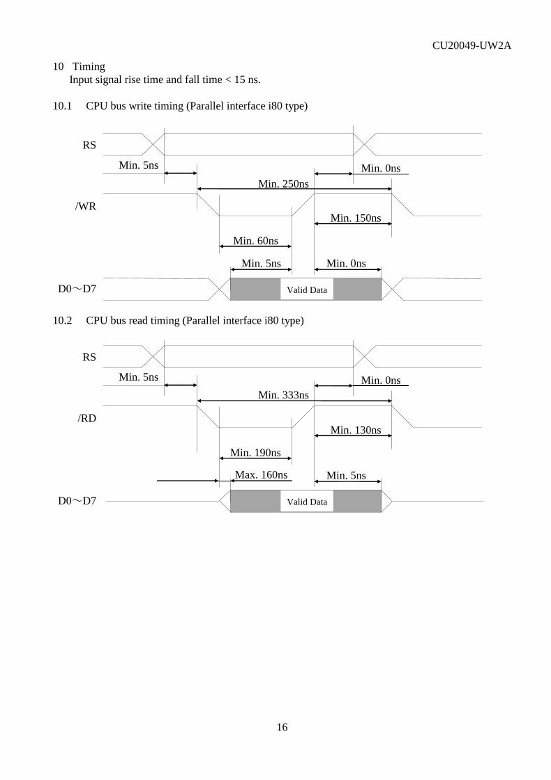
10 Timing
Input signal rise time and fall time < 15 ns.
10.1 CPU bus write timing (Parallel interface i80 type)
10.2 CPU bus read timing (Parallel interface i80 type)
Min. 250ns
Min. 150ns
Min. 5ns
Min. 0ns
Min. 0ns
Min. 5ns
Valid Data
RS
/WR
D0~D7
Min. 60ns
Min. 333ns
Max. 160ns
Min. 130ns
Min. 5ns
Min. 5ns
Min. 0ns
RS
/RD
D0~D7
Min. 190ns
Valid Data

CU20049-UW2A
17
10.3 CPU bus write timing (Parallel interface M68 type)
10.4 CPU bus read timing (Parallel interface M68 type)
Min. 500ns
Min. 20ns
Min. 230ns Min. 230ns
Min 5ns
Min. 10ns
Max. 160ns
RS
E
D0~D7
R/W
Valid Data
Min. 20ns
Min. 10ns Min. 80ns
Min. 500ns
Min. 230ns Min. 230ns
Min. 10ns
RS
E
D0~D7
R/W
Valid Data

CU20049-UW2A
18
10.5 Write timing (Serial interface)
10.6 Read timing (Serial interface)
Valid
data
1
0
STB
SI/SO
SCK
Min.
500ns 1
0
1
0
Min.
200ns
Min.
500ns
Min.
200ns
Min.
500ns
Max.
150ns
Max.
30ns
Input
Valid
data
STB
SCK
SI
Min.
500ns 1
0
1
0
Min.
200ns
Min.
500ns
Min.
200ns
Min.
100ns
Min.
500ns
Min.
100ns Min.
100ns
1
0

CU20049-UW2A
19
11 Connector Pin assignment
The through holes are prepared for power supply and data communications.
A connector or pins may be able to solder to the holes.
Diameter of holes is 1.0mm.
11.1 14pin Connector (CN1) for parallel interface
Pin No. Signal name Function Direction
1 GND Ground Input
2 VCC Power supply Input
3 NC * Non connection -
4 RS Switch signal Input
5 R/W(WR) Data transfer select
(Write enable)
Input
6 E(RD) Write enable
(Read enable)
Input
7 DB0 Data input/output Input/Output
8 DB1 Data input/output Input/Output
9 DB2 Data input/output Input/Output
10 DB3 Data input/output Input/Output
11 DB4 Data input/output Input/Output
12 DB5 Data input/output Input/Output
13 DB6 Data input/output Input/Output
14 DB7 Data input/output Input/Output
*: The third through hole is for reset input when No 1 and No 2 of JP4 are short.
(): At the i80 type.
11.2 6pin Connector (CN3) for serial interface
Pin No. Signal name Function Direction
1 VCC Power supply Input
2 SI/SO Data input/output Input/Output
3 GND Ground Input
4 STB Strobe Input
5 SCK Display clock Input
6 NC * Non connection -
*: The 6th through hole is for reset input when No.1 and No.2 of JP4 are short.

CU20049-UW2A
20
12 Outline dimension

CU20049-UW2A
21
Notice for the Cautious Handling VFD Modules
Handling and Usage Precautions: Please carefully follow the appropriate product application notes for proper usage, safety handling, and operation standards for maximum performance. [VFD tubes are made of glass]
Because the edges of the VFD glass-envelop are not smooth, it is necessary to handle carefully to avoid injuries to your hands.
Please avoid breaking the VFD glass-envelop to prevent injury from sharp glass particles.
The tip of the exhaust pipe is fragile so avoid shock from impact.
It is recommended to allow sufficient open space surrounding the exhaust pipe to avoid possible damage.
Please design the PCB for the VFD-module within 0.3 mm warping tolerance to avoid any forces that may damage the display due to PCB distortion causing a breakdown of the electrical circuit leading to VFD failure.
[High voltage]
Avoid touching conductive electrical parts, because the VFD-module uses high voltage exceeding 30~100 volts.
Even when electric power is turned off, it may take more than one minute for the electrical current to discharge. [Cable connection]
Do not unplug the power and/or data cables of VFD-modules during operating condition because unrecoverable damage may result.
Sending input signals to the VFD-module during a power off condition sometimes causes I/O port damage.
It is recommended to use a 30 cm or shorter signal cable to prevent functional failures. [Electrostatic charge]
VFD-modules need electrostatic free packaging and protection from electrostatic charges during handling and usage. [Structure]
During operation, VFD and VFD-modules generate heat. Please consider sufficient heat radiation dissipation using heat sink solutions.
We prefer to use UL grade materials or components in conjunction with VFD-modules.
Wrap and twist motion causes stress and may break VFDs & VFD modules. Please adhere to allowances within 0.3mm at the point of attachment.
[Power]
Apply regulated power to the VFD-module within specified voltages to protect from failures.
Because some VFD-modules may consume in rush current equal to twice the typical current at power-on timing, we recommend using a sufficient power capability and quick starting of the power regulator.
VFD-module needs a specified voltage at the point of connection. Please use an adequate power cable to avoid a decrease in voltage. We also recommend inserting a power fuse for extra protection.
[Operating consideration]
Illuminating phosphor will decrease in brightness during extended operation. If a fixed pattern illuminates for an extended period (several hours), the phosphor efficiency will decrease compared to the non operating phosphor causing a non uniform brightness among pixels. Please consider programming the display patterns to use all phosphor segments evenly. Scrolling may be a consideration for a period of time to refresh the phosphor condition and improve even illumination to the pixels.
We recommend using a signal cable 30cm or less to avoid some possible disturbances to the signal. [Storage and operating environment]
Please use VFD-modules under the recommended specified environmental conditions. Salty, sulfur and dusty environments may damage the VFD-module even during storage.
[Discard]
Some VFDs contain a small amount of cadmium in the phosphor and lead in the solder. When discarding VFDs or VFD-modules, please adhere to governmental related laws or regulations. (Note: RoHS-compliant products do not contain cadmium)
[Others]
Although the VFD-module is designed to be protected from electrical noise, please plan your circuitry to exclude as much noise as possible.
Do not reconstruct or repair the VFD-module without our authorization. We cannot assure the quality or reliability of unauthorized reconstructed VFD-modules.
Notice:
We do not authorize the use of any patents that may be inherent in these specifications.
Neither whole nor partial copying of this specification is permitted without our approval. If necessary, please ask for assistance from our sales consultant.
This product is not designed for military, aerospace, medical or other life-critical applications. If you choose to use this product for these applications, please ask us for prior consultation or we cannot take responsibility for problems that may occur.