
Robust nano-fabrication of an integrated platform for spin control...
8
Robust nano-fabrication of an integrated platform for spin control in a tunable microcavity Stefan Bogdanović, Madelaine S. Z. Liddy, Suzanne B. van Dam, Lisanne C. Coenen, Thomas Fink, Marko Lončar, and Ronald Hanson Citation: APL Photonics 2, 126101 (2017); doi: 10.1063/1.5001144 View online: https://doi.org/10.1063/1.5001144 View Table of Contents: http://aip.scitation.org/toc/app/2/12 Published by the American Institute of Physics Articles you may be interested in Single-photon detectors combining high efficiency, high detection rates, and ultra-high timing resolution APL Photonics 2, 111301 (2017); 10.1063/1.5000001 Dielectric broadband meta-vector-polarizers based on nematic liquid crystal APL Photonics 2, 126102 (2017); 10.1063/1.5006016 Accessing the dark exciton spin in deterministic quantum-dot microlenses APL Photonics 2, 121303 (2017); 10.1063/1.5004147 Nanodiamonds with photostable, sub-gigahertz linewidth quantum emitters APL Photonics 2, 116103 (2017); 10.1063/1.4998199 Lasing at 602-620 nm from a red algae-derived phycobiliprotein APL Photonics 2, 121301 (2017); 10.1063/1.4999716 Multi-planar amorphous silicon photonics with compact interplanar couplers, cross talk mitigation, and low crossing loss APL Photonics 2, 116101 (2017); 10.1063/1.5000384
Transcript of Robust nano-fabrication of an integrated platform for spin control...

Robust nano-fabrication of an integrated platform for spin control in a tunablemicrocavityStefan Bogdanović, Madelaine S. Z. Liddy, Suzanne B. van Dam, Lisanne C. Coenen, Thomas Fink, MarkoLončar, and Ronald Hanson
Citation: APL Photonics 2, 126101 (2017); doi: 10.1063/1.5001144View online: https://doi.org/10.1063/1.5001144View Table of Contents: http://aip.scitation.org/toc/app/2/12Published by the American Institute of Physics
Articles you may be interested in Single-photon detectors combining high efficiency, high detection rates, and ultra-high timing resolutionAPL Photonics 2, 111301 (2017); 10.1063/1.5000001
Dielectric broadband meta-vector-polarizers based on nematic liquid crystalAPL Photonics 2, 126102 (2017); 10.1063/1.5006016
Accessing the dark exciton spin in deterministic quantum-dot microlensesAPL Photonics 2, 121303 (2017); 10.1063/1.5004147
Nanodiamonds with photostable, sub-gigahertz linewidth quantum emittersAPL Photonics 2, 116103 (2017); 10.1063/1.4998199
Lasing at 602-620 nm from a red algae-derived phycobiliproteinAPL Photonics 2, 121301 (2017); 10.1063/1.4999716
Multi-planar amorphous silicon photonics with compact interplanar couplers, cross talk mitigation, and lowcrossing lossAPL Photonics 2, 116101 (2017); 10.1063/1.5000384

APL PHOTONICS 2, 126101 (2017)
Robust nano-fabrication of an integrated platformfor spin control in a tunable microcavity
Stefan Bogdanovic,1,a Madelaine S. Z. Liddy,2,a Suzanne B. van Dam,1
Lisanne C. Coenen,1 Thomas Fink,3 Marko Loncar,4 and Ronald Hanson1,b1QuTech, Delft University of Technology, P.O. Box 5046, 2600 GA Delft, The Netherlands2Department of Electrical and Computer Engineering, Institute for Quantum Computing,University of Waterloo, Waterloo, Ontario N2L 3G1, Canada3Institute of Quantum Electronics, ETH Zurich, CH-8093 Zurich, Switzerland4John A. Paulson School of Engineering and Applied Sciences, Harvard University, Cambridge,Massachusetts 02138, USA
(Received 22 August 2017; accepted 1 November 2017; published online 21 November 2017)
Coupling nitrogen-vacancy (NV) centers in diamonds to optical cavities is a promis-ing way to enhance the efficiency of diamond-based quantum networks. An essentialaspect of the full toolbox required for the operation of these networks is the abilityto achieve the microwave control of the electron spin associated with this defectwithin the cavity framework. Here, we report on the fabrication of an integratedplatform for the microwave control of an NV center electron spin in an open, tun-able Fabry–Perot microcavity. A critical aspect of the measurements of the cavity’sfinesse reveals that the presented fabrication process does not compromise its opticalproperties. We provide a method to incorporate a thin diamond slab into the cav-ity architecture and demonstrate the control of the NV center spin. These resultsshow the promise of this design for future cavity-enhanced NV center spin-photonentanglement experiments. © 2017 Author(s). All article content, except where oth-erwise noted, is licensed under a Creative Commons Attribution (CC BY) license(http://creativecommons.org/licenses/by/4.0/). https://doi.org/10.1063/1.5001144
I. INTRODUCTION
Nitrogen-vacancy (NV) colour centers in diamonds have emerged as attractive candidates forquantum photonic applications. Their electronic spin can be optically initialized, read out in a singleshot,1 and coherently manipulated with the use of microwave signals.2 This spin-photon interface pro-vides a platform for distant entanglement generation,3 while additional coupling to nearby carbon-13nuclear spins forms a multi-qubit quantum node.4–7 These aspects make the NV center a good candi-date for quantum network protocols.8–10 The efficiency of entanglement generation between networknodes is currently limited by the NV center’s low (≈3%) emission rate of the resonant zero-phonon line(ZPL) photons. This problem can be addressed by coupling NV centers to optical microcavities,11–23
enhancing the ZPL emission rate and providing efficient photon extraction by means of the Purcelleffect.24 An appealing cavity design consists of an open, tunable Fabry–Perot microcavity housing alarge-area diamond membrane25–27 in which emitters retain their bulk-like properties.28 The tunabil-ity of this design enables both the spectral positioning of the cavity to be resonant with the emitter aswell as the selective lateral placement of the emitter within the center of the cavity mode. However,in order to use these emitters in quantum information protocols, a microwave control must be inte-grated into the cavity architecture. Here, we present fabrication methods used to create a platform thatintegrates the microwave control of an NV center spin within an optical cavity while maintaining thecavity’s high finesse properties. While microwave addressing of a single NV center spin has already
aS. Bogdanovic and M. S. Z. Liddy contributed equally to this work.bElectronic mail: [email protected]
2378-0967/2017/2(12)/126101/7 2, 126101-1 © Author(s) 2017

126101-2 Bogdanovic et al. APL Photonics 2, 126101 (2017)
FIG. 1. Fabrication of the Fabry–Perot cavity components. (a) The design of the Fabry–Perot cavity comprised a processedplanar mirror and laser ablated fiber interface. (b) Phase profile of the ablated fiber facet measured using an interferometer.(c) Reconstructed surface profile of the region denoted by the black rectangle in (b) (blue line) and fit with a Gaussianfunction on a linear slope accounting for the tilted fiber plane (green line). The extracted parameters are d = 8.3 µm andzt = 403 nm. The fiber radius of curvature R is 22.4 µm. (d) Planar mirror processing stages: (i) Mirror coatings consist of31 layers of alternating high (Ta2O5, 75 nm thickness) and low (SiO2, 100 nm thickness) refractive index materials depositedonto a low roughness fused silica plate and ablated fiber tip. (ii) Patterned and developed optical photoresist mask for themicrowave striplines. (iii) Etching 65 nm of the material into the mirror stack using an SF6 and O2 ICP RIE recipe followedby (iv) evaporation of 5 nm (65 nm) of titanium (gold) and an overnight lift-off. (v) Patterned and developed optical resistmask for marker array, aligned to the gold striplines. (vi) Evaporation of 5 nm (5 nm) titanium (gold) followed by 1 h oflift-off. (e) Cross section of the mirror post processing revealing the embedded microwave striplines and surface markerarray.
been realized in thin diamond slabs29 and photonic crystal cavities,21 this is the first demonstrationof the NV center spin addressing within a framework tailored to the implementation of a tunablemicrocavity.
The cavity consists of a dimpled fiber tip and polished fused silica plate, both coated with a highlyreflective dielectric mirror stack [Fig. 1(a)]. Microwave striplines and marker arrays are fabricated onthe planar mirror surface in order to locate the NV centers and address their spin within the diamondslab bonded to the mirror.
II. FABRICATION OF CAVITY COMPONENTS
A. Fiber dimple
The curved fiber profile was fabricated using a CO2 laser ablation technique:30,31 A single1 ms long circularly polarized laser pulse is focused onto the cleaved fiber facet. As a result ofthermal evaporation and subsequent melting, a concave depression with low surface roughness ofσrms . 0.20 ± 0.02 nm is created. The depth and diameter of this depression can be controlled byvarying a combination of the pulse power, duration, and beam waist. Due to the small fiber corediameter, care must be taken to center the depression onto the cleaved facet to ensure a good couplingefficiency to the cavity mode. Following dimple creation, the surface geometry is measured, in situ,with an interferometer. Figure 1(b) shows an exemplary phase measurement and the correspondingreconstructed surface profile [Fig. 1(c)]. The shape of the depression closely resembles that of a two-dimensional Gaussian. In its center, it can be approximated by a hemisphere with radius of curvature,R≈ d2/ (8zt), where d and zt are the diameter and depth of the dimple, respectively.30 Low-ellipticityprofiles with comparable radii of curvature along the x- and y-directions are required in order tominimize polarization splitting of the cavity mode.32 The extracted ellipticity of the fiber used in thisexperiment is 1.3%.

126101-3 Bogdanovic et al. APL Photonics 2, 126101 (2017)
B. Mirror coatings
Following laser ablation of the fibers, a mirror stack forming a Distributed Bragg Reflec-tor (DBR) is deposited onto both the fiber facets and polished fused silica plates (Laseroptik).The residual transmission of this stack is measured to be 50 ppm at 637 nm wavelength. Theobserved fiber and specified fused silica surface roughness (0.2 nm and 0.5 nm RMS, respec-tively) correspond to the scattering losses of 25 and 100 ppm.33 Following coating, the planarmirror is annealed in vacuum at 300 ◦C for 5 h, which reduces the absorption losses of the stackfrom ≈50 ppm to ≤10 ppm.34 The total losses give an expected value of the cavity finesse ofF ≈ 22 000.
C. Striplines and marker field
In order to address the spin and index the location of the NV centers, parallel microwave striplinesand a field of uniquely identifiable markers are fabricated on the planar mirror surface. For successfuldiamond bonding, the processed mirrors must possess a low profile for all patterned surface features.A two-step fabrication procedure was devised, which includes first patterning embedded microwavestriplines into the planar mirror, followed by the deposition of a small marker array on the surface. Theseparate fabrication is necessary since etching both the markers and the striplines into the mirror gavepoor liftoff results, which interfered with the diamond bonding procedure. The fabrication procedureis presented in Fig. 1(d). To begin the processing, optical photoresist, AZ 3007, is deposited on the pla-nar mirror at a thickness of 1 µm, followed by a soft bake at 90 ◦C for 60 s. 4 mm long by 45 µm widemasks for the striplines are patterned with a laser writer (DMO Microwriter ML-2) and developed inMF-321 for 45 s [Figs. 1(d-i) and 1(d-ii)]. Using an SF6- and O2-based Inductively Coupled PlasmaReactive Ion Etch (ICP RIE) to remove 65 nm of the material, the mask for the microwave striplinesis transferred into the planar mirror [Fig. 1(d-iii)] (Sec. II). After etching, a 5-nm layer of titanium isevaporated as an adhesion layer followed by 65 nm of gold (Temescal FC2000). The first stage of thefabrication is completed by removing all excess gold with an overnight lift-off in a photoresist stripper(PRS) at 70 ◦C, leading to the result shown in [Fig. 1(d-iv)]. The second stage of the fabrication proce-dure proceeds with the same photoresist deposition method, followed by patterning the marker array,aligned adjacent to the microwave striplines, and then developed [Fig. 1(d-v)]. 5 nm layers of Ti andAu are evaporated consecutively, followed by 1 h of lift-off in PRS at 70 ◦C to complete the fabrication[Fig. 1(d-vi)].
Essential to the desired cavity architecture is the possibility to bond a several micrometer thindiamond membrane over the structures on the planar mirror. Irregular structures and frills on theedges of the fabricated striplines have been found to deter successful bonding. Furthermore, amicrowave stripline that is fully recessed in the etched trench acts as a capillary channel for waterused during the bonding process, preventing a good diamond-mirror bond. A uniform raised profileof a feature above the mirror surface by no more than 20 nm was found to allow for successfulbonding.
III. CAVITY PERFORMANCE
In order to preserve the optical performance of the cavity, mirror coatings must not be damagedor have surface residues left as a result of the processing described in the Sec. C. To verify that thepresented fabrication procedure does not introduce additional losses to the planar mirror, the finesseof a cavity with a processed and unprocessed planar mirror is compared while keeping the fibermirror unaltered. The finesse F is calculated from the cavity linewidth δν and free spectral range(FSR) νFSR,
F =νFSR
δν=
c2 · Lcav · δν
, (1)
where c is the speed of light and Lcav is the cavity length.The cavity linewidth is obtained by exciting the cavity with a 637-nm laser through the fiber
port while modulating the planar mirror position with a 40-Hz sinusoidal signal scanning the cavity
126101-4 Bogdanovic et al. APL Photonics 2, 126101 (2017)
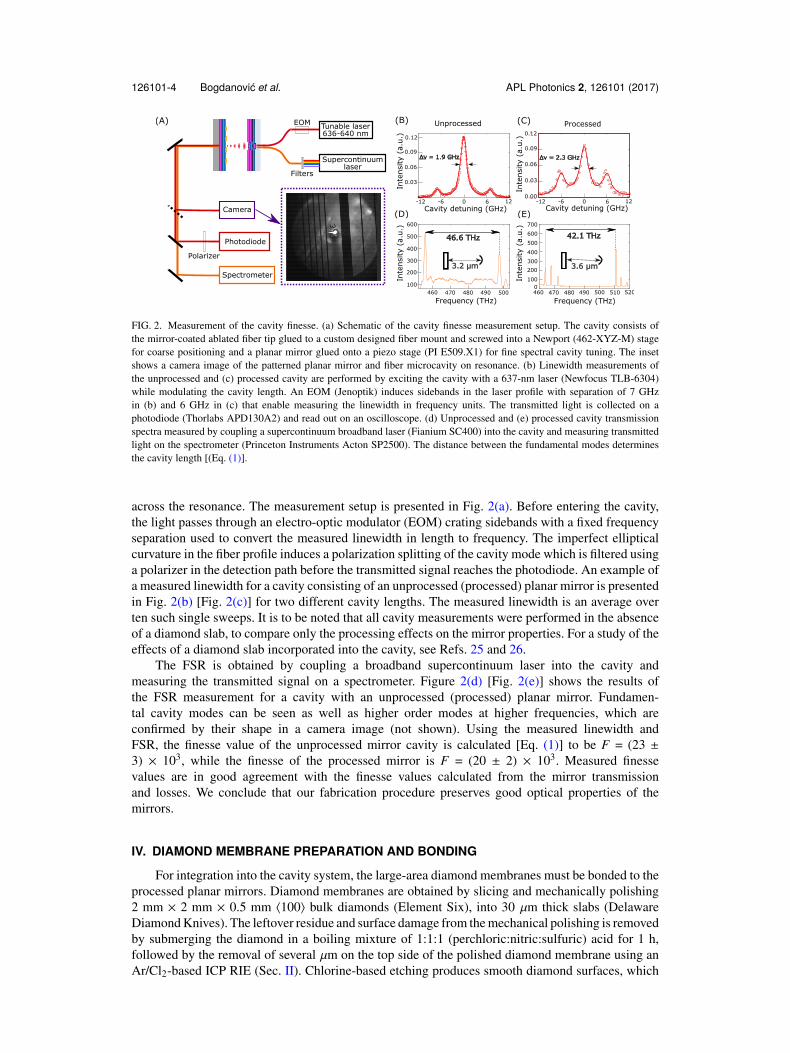
FIG. 2. Measurement of the cavity finesse. (a) Schematic of the cavity finesse measurement setup. The cavity consists ofthe mirror-coated ablated fiber tip glued to a custom designed fiber mount and screwed into a Newport (462-XYZ-M) stagefor coarse positioning and a planar mirror glued onto a piezo stage (PI E509.X1) for fine spectral cavity tuning. The insetshows a camera image of the patterned planar mirror and fiber microcavity on resonance. (b) Linewidth measurements ofthe unprocessed and (c) processed cavity are performed by exciting the cavity with a 637-nm laser (Newfocus TLB-6304)while modulating the cavity length. An EOM (Jenoptik) induces sidebands in the laser profile with separation of 7 GHzin (b) and 6 GHz in (c) that enable measuring the linewidth in frequency units. The transmitted light is collected on aphotodiode (Thorlabs APD130A2) and read out on an oscilloscope. (d) Unprocessed and (e) processed cavity transmissionspectra measured by coupling a supercontinuum broadband laser (Fianium SC400) into the cavity and measuring transmittedlight on the spectrometer (Princeton Instruments Acton SP2500). The distance between the fundamental modes determinesthe cavity length [(Eq. (1)].
across the resonance. The measurement setup is presented in Fig. 2(a). Before entering the cavity,the light passes through an electro-optic modulator (EOM) crating sidebands with a fixed frequencyseparation used to convert the measured linewidth in length to frequency. The imperfect ellipticalcurvature in the fiber profile induces a polarization splitting of the cavity mode which is filtered usinga polarizer in the detection path before the transmitted signal reaches the photodiode. An example ofa measured linewidth for a cavity consisting of an unprocessed (processed) planar mirror is presentedin Fig. 2(b) [Fig. 2(c)] for two different cavity lengths. The measured linewidth is an average overten such single sweeps. It is to be noted that all cavity measurements were performed in the absenceof a diamond slab, to compare only the processing effects on the mirror properties. For a study of theeffects of a diamond slab incorporated into the cavity, see Refs. 25 and 26.
The FSR is obtained by coupling a broadband supercontinuum laser into the cavity andmeasuring the transmitted signal on a spectrometer. Figure 2(d) [Fig. 2(e)] shows the results ofthe FSR measurement for a cavity with an unprocessed (processed) planar mirror. Fundamen-tal cavity modes can be seen as well as higher order modes at higher frequencies, which areconfirmed by their shape in a camera image (not shown). Using the measured linewidth andFSR, the finesse value of the unprocessed mirror cavity is calculated [Eq. (1)] to be F = (23 ±3) × 103, while the finesse of the processed mirror is F = (20 ± 2) × 103. Measured finessevalues are in good agreement with the finesse values calculated from the mirror transmissionand losses. We conclude that our fabrication procedure preserves good optical properties of themirrors.
IV. DIAMOND MEMBRANE PREPARATION AND BONDING
For integration into the cavity system, the large-area diamond membranes must be bonded to theprocessed planar mirrors. Diamond membranes are obtained by slicing and mechanically polishing2 mm × 2 mm × 0.5 mm 〈100〉 bulk diamonds (Element Six), into 30 µm thick slabs (DelawareDiamond Knives). The leftover residue and surface damage from the mechanical polishing is removedby submerging the diamond in a boiling mixture of 1:1:1 (perchloric:nitric:sulfuric) acid for 1 h,followed by the removal of several µm on the top side of the polished diamond membrane using anAr/Cl2-based ICP RIE (Sec. II). Chlorine-based etching produces smooth diamond surfaces, which

126101-5 Bogdanovic et al. APL Photonics 2, 126101 (2017)
is required to minimize the scattering loss at the diamond interface within the cavity.36,37 The finaldiamond roughness, measured with atomic force microscopy, was found to be 0.2 nm RMS. However,prolonged exposure to chlorine etch gas has been linked to degrading optical properties of the NVcenters. Introducing an O2-based plasma etching step has been found to resolve the surface chlorinecontamination.27,28
In order to preserve optical properties of the cavity, the diamond must be fixed to the mirrorwithout adhesives, constraining the type of bonding techniques permitted. First attempts to etchthe diamond slab with the bottom surface coated with the dielectric mirror stack resulted in coatingdelamination, likely due to the difference in thermal expansion coefficients of the materials. Successfulbonding of the diamond membrane to a processed planar mirror with an activated hydrophilic surfacehas been achieved via van der Waals forces. The addition of a water droplet between the two interfacespromotes bonding via strong interfacial forces creating good optical contact between the diamondand the mirror, removing the need for adhesives.38,39
To prepare the processed mirror for bonding, it is placed in an oxygen plasma environment at0.4 mbar for 45 s with 100 W, altering the hydrophobicity of the surface [Fig. 3(a-i)]. Water is pipettedonto the surface of the mirror [Fig. 3(a-ii)] followed by placing the diamond membrane on top ofa patterned region. Using the light from an optical microscope objective, the water is evaporatedwhile the bonding process is monitored simultaneously [Fig. 3(a-iii)]. The quality of the bond canbe evaluated with visual cues as well as with a profile measurement. Figures 3(a-iv) and 3(b) showSEM and optical images, respectively, of the bonded diamond. A poor bond can be identified by theappearance of Newton rings, indicative of an uneven surface and the existence of an air gap betweenthe mirror and diamond. In the optical image, a well-bonded diamond is indicated by a uniformcolouration. The “milky” colouration seen near the striplines highlights the slightly elevated areas.
FIG. 3. Diamond membrane bonding and NV center spin control. (a) Diamond bonding to the patterned mirror: (i) Surfaceactivation of the processed mirror chip with an oxygen plasma at low vacuum. (ii) Water is pipetted onto the activated surface.(iii) The diamond membrane is placed onto the patterned surface followed by drying of the water using the light from themicroscope objective. (iv) The diamond membrane containing NV centers is bonded to the mirror. Inset: A scanning electronmicroscope (SEM) image of a bonded diamond membrane atop a patterned planar mirror. (b) Optical image of an etched2 mm × 2 mm × 8 µm diamond, bonded to the processed planar mirror with microwave striplines and marker array.(c) Scanning optical confocal image showing a single NV center (inset). The scans were performed at the depth of≈1.5 µm below the surface of the diamond membrane. The 2 µm × 2 µm spots correspond to the photoluminescencefrom the square gold markers. Part of the microwave stripline is visible on the left. (d) Optically detected electron spin res-onance spectrum demonstrating NV spin addressing with the embedded microwave striplines. The spectrum exhibits tworesonances associated with the ms = 0→ ms = ±1 spin transitions (inset), centered at the zero field splitting Dgs = 2.87 GHz.Two resonances are separated by the Zeeman splitting 2γeBz where γe is the NV electron spin gyromagnetic ration andBz is the static external magnetic field. Individual electron spin resonance dips are fitted using three Lorentzian profileswith a splitting of 2.16 MHz to account for the hyperfine splitting from the NV interaction with its host 14N nuclear spin(IN = 1).35

126101-6 Bogdanovic et al. APL Photonics 2, 126101 (2017)
Profilometer measurements revealed an overall height variation of 100 nm over the diamond surfacebonded on top of the patterned area.
V. ELECTRON SPIN ADDRESSING
A scanning confocal microscope is used for fluorescence imaging of the NV centers underambient conditions with off-resonant laser excitation at 532 nm. The NV centers were located inclose proximity to the marker field such that they can be easily indexed and located again [Fig. 3(c)].The embedded microwave stripline, seen on the left portion of the confocal scan in Fig. 3(c), isused to identify and address the ms = 0 → ms = ±1 NV center spin transitions40,41 in the presenceof a static magnetic field Bz ≈ 10 G. The optically detected electron spin resonance spectrum isshown in Fig. 3(d). This demonstrates our ability to address NV center spin with microwaves whencombining the stripline fabrication and diamond bonding technique.
VI. CONCLUSION
In conclusion, we have presented the fabrication of an integrated platform for microwave controlin an open, high finesse Fabry–Perot microcavity enclosing a thin diamond membrane. Finessemeasurements of the processed mirrors confirm that the fabrication procedure does not compromisetheir optical properties. We present a diamond bonding method that allows placing large-area diamondmembranes onto the cavity mirror while simultaneously enabling the microwave control of the NVcenter spin. The presented cavity architecture is well suited for enabling the enhancement of the NVcenters resonant emission along with the control of their spins.
VII. METHODS
Markers and stripline etching procedure: The planar mirrors are etched with an SF6- and O2-basedICP RIE technique in an (Oxford Instruments PlasmaLab 100) etcher with the following parame-ters: SF6(Ar) gas flow—50(10) sccm, ICP (RF) power—700(150) W, base pressure—0.026 mbar,temperature—50 ◦C, time—26 s followed by O2 gas flow—50 sccm, ICP(RF) power—750(20) W,base pressure—0.030 mbar, temperature—50 ◦C, time—8 s at a combined rate of 1.9 nm/s, removing65 nm of mirror material.
The diamond etch parameters are as follows: Ar(Cl2) gas flow—10(20) sccm, ICP (RF) power—500(200) W, base pressure—0.01 mbar, temperature—30 ◦C with a resulting etch rate of 2.5 µm/h.
ACKNOWLEDGMENTS
The authors wish to thank P. Latawiec for helpful discussions. M.L. wishes to acknowledge thesupport of QuTech during his sabbatical stay. M.S.Z.L. acknowledges the Dutch Liberation Schol-arship Programme. This work was supported by the Dutch Organization for Fundamental Researchon Matter (FOM), Dutch Technology Foundation (STW), the Netherlands Organization for Scien-tific Research (NWO) through a VICI grant, the EU S3NANO program, and the European ResearchCouncil through a Starting Grant.
1 L. Robledo, L. Childress, H. Bernien, B. Hensen, P. F. A. Alkemade, and R. Hanson, Nature 477, 574–578 (2011).2 F. Jelezko, T. Gaebel, I. Popa, A. Gruber, and J. Wrachtrup, Phys. Rev. Lett. 92, 076401 (2004).3 H. Bernien, B. Hensen, W. Pfaff, G. Koolstra, M. S. Blok, L. Robledo, T. H. Taminiau, M. Markham, D. J. Twitchen,
L. Childress, and R. Hanson, Nature 497, 86–90 (2013).4 M. V. G. Dutt, L. Childress, L. Jiang, E. Togan, J. Maze, F. Jelezko, A. S. Zibrov, P. R. Hemmer, and M. D. Lukin, Science
316, 1312–1316 (2007).5 P. Neumann, J. Beck, M. Steiner, F. Rempp, H. Fedder, P. R. Hemmer, J. Wrachtrup, and F. Jelezko, Science 329, 542–544
(2010).6 T. H. Taminiau, J. J. T. Wagenaar, T. van der Sar, F. Jelezko, V. V. Dobrovitski, and R. Hanson, Phys. Rev. Lett. 109, 137602
(2012).7 A. Reiserer, N. Kalb, M. S. Blok, K. J. M. van Bemmelen, T. H. Taminiau, R. Hanson, D. J. Twitchen, and M. Markham,
Phys. Rev. X 6, 021040 (2016).8 H. J. Kimble, Nature 453, 1023–1030 (2008).

126101-7 Bogdanovic et al. APL Photonics 2, 126101 (2017)
9 N. Kalb, A. A. Reiserer, P. C. Humphreys, J. J. W. Bakermans, S. J. Kamerling, N. H. Nickerson, S. C. Benjamin,D. J. Twitchen, M. Markham, and R. Hanson, Science 356, 928–932 (2017).
10 S. B. van Dam, P. C. Humphreys, F. Rozpedek, S. Wehner, and R. Hanson, Quantum Sci. Technol. 2, 034002 (2017).11 J. Wolters, A. W. Schell, G. Kewes, N. Nusse, M. Schoengen, H. Doscher, T. Hannappel, B. Lochel, M. Barth, and O. Benson,
Appl. Phys. Lett. 97, 141108 (2010).12 P. E. Barclay, K. M. C. Fu, C. Santori, A. Faraon, and R. G. Beausoleil, Phys. Rev. X 1, 011007 (2011).13 T. van der Sar, J. Hagemeier, W. Pfaff, E. C. Heeres, S. M. Thon, H. Kim, P. M. Petroff, T. H. Oosterkamp, D. Bouwmeester,
and R. Hanson, Appl. Phys. Lett. 98, 193103 (2011).14 A. Faraon, C. Santori, Z. Huang, V. M. Acosta, and R. G. Beausoleil, Phys. Rev. Lett. 109, 033604 (2012).15 H. Kaupp, C. Deutsch, H.-C. Chang, J. Reichel, T. W. Hansch, and D. Hunger, Phys. Rev. A 88, 053812 (2013).16 R. Albrecht, A. Bommer, C. Deutsch, J. Reichel, and C. Becher, Phys. Rev. Lett. 110, 243602 (2013).17 B. J. M. Hausmann, B. J. Shields, Q. Quan, Y. Chu, N. P. de Leon, R. Evans, M. J. Burek, A. S. Zibrov, M. Markham,
D. J. Twitchen, H. Park, M. D. Lukin, and M. Loncar, Nano Lett. 13, 5791 (2013).18 J. C. Lee, D. O. Bracher, S. Cui, K. Ohno, C. A. McLellan, X. Zhang, P. Andrich, B. Aleman, K. J. Russell, A. P. Magyar,
I. Aharonovich, A. Bleszynski Jayich, D. Awschalom, and E. L. Hu, Appl. Phys. Lett. 105, 261101 (2014).19 J. Riedrich-Moller, S. Pezzagna, J. Meijer, C. Pauly, F. Mucklich, M. Markham, A. M. Edmonds, and C. Becher, Appl.
Phys. Lett. 106, 221103 (2015).20 D. Englund, B. Shields, K. Rivoire, F. Hatami, J. Vuckovic, H. Park, and M. D. Lukin, Nano Lett. 10, 3922 (2010).21 L. Li, T. Schroder, E. H. Chen, M. Walsh, I. Bayn, J. Goldstein, O. Gaathon, M. E. Trusheim, M. Lu, J. Mower, M. Cotlet,
M. L. Markham, D. J. Twitchen, and D. Englund, Nat. Commun. 6, 6173 (2015).22 S. Johnson, P. R. Dolan, T. Grange, A. A. P. Trichet, G. Hornecker, Y. C. Chen, L. Weng, G. M. Hughes, A. A. R. Watt,
A. Auffeves, and J. M. Smith, New J. Phys. 17, 122003 (2015).23 H. Kaupp, T. Hummer, M. Mader, B. Schlederer, J. Benedikter, P. Haeusser, H.-C. Chang, H. Fedder, T. W. Hansch, and
D. Hunger, Phys. Rev. Appl. 6, 054010 (2016).24 E. M. Purcell, H. C. Torrey, and R. V. Pound, Phys. Rev. 69, 37 (1946).25 E. Janitz, M. Ruf, M. Dimock, A. Bourassa, J. Sankey, and L. Childress, Phys. Rev. A 92, 043844 (2015).26 S. Bogdanovic, S. B. van Dam, C. Bonato, L. C. Coenen, A. J. Zwerver, B. Hensen, M. S. Z. Liddy, T. Fink, A. Reiserer,
M. Loncar, and R. Hanson, Appl. Phys. Lett. 110, 171103 (2017).27 D. Riedel, I. Sollner, B. J. Shields, S. Starosielec, P. Appel, E. Neu, P. Maletinsky, and R. J. Warburton, Phys. Rev. X 7,
031040 (2017).28 Y. Chu, N. de Leon, B. Shields, B. Hausmann, R. Evans, E. Togan, M. J. Burek, M. Markham, A. Stacey, A. Zibrov,
A. Yacoby, D. Twitchen, M. Loncar, H. Park, P. Maletinsky, and M. Lukin, Nano Lett. 14, 1982 (2014).29 J. S. Hodges, L. Li, M. Lu, E. H. Chen, M. E. Trusheim, S. Allegri, X. Yao, O. Gaathon, H. Bakhru, and D. Englund, New
J. Phys. 14, 093004 (2012).30 D. Hunger, T. Steinmetz, Y. Colombe, C. Deutsch, T. W. Hansch, and J. Reichel, New J. Phys. 12, 065038 (2010).31 D. Hunger, C. Deutsch, R. J. Barbour, R. J. Warburton, and J. Reichel, AIP Adv. 2, 012119 (2012).32 M. Uphoff, M. Brekenfeld, G. Rempe, and S. Ritter, New J. Phys. 17, 13053 (2014).33 T. Klaassen, M. P. van Exter, and J. P. Woerdman, Appl. Opt. 46, 5210 (2007).34 Laseroptik, internal communication (2016).35 P. Neumann, R. Kolesov, V. Jacques, J. Beck, J. Tisler, A. Batalov, L. Rogers, N. B. Manson, G. Balasubramanian, F. Jelezko,
and J. Wrachtrup, New J. Phys. 11, 013017 (2009).36 J. Enlund, J. Isberg, M. Karlsson, F. Nikolajeff, J. Olsson, and D. J. Twitchen, Carbon 43, 1839 (2005).37 C. Lee, E. Gu, M. Dawson, I. Friel, and G. Scarsbrook, Diamond Relat. Mater. 17, 1292 (2008).38 E. Yablonovitch, D. M. Hwang, T. J. Gmitter, L. T. Florez, and J. P. Harbison, Appl. Phys. Lett. 56, 2419–2421 (1990).39 P. Latawiec, V. Venkataraman, M. J. Burek, B. J. M. Hausmann, I. Bulu, and M. Loncar, Optica 2, 924 (2015).40 A. Gruber, A. Drabenstedt, C. Tietz, L. Fleury, J. Wrachtrup, and C. von Borczyskowski, Science 276, 2012–2014 (1997).41 G. Balasubramanian, I. Y. Chan, R. Kolesov, M. Al-Hmoud, J. Tisler, C. Shin, C. Kim, A. Wojcik, P. R. Hemmer, A. Krueger,
T. Hanke, A. Leitenstorfer, R. Bratschitsch, F. Jelezko, and J. Wrachtrup, Nature 455, 648–651 (2008).


