RMI 6 11 HIN- AM9468 SINGLE PHASE FULL WAVE DIRECT PWM ... · SINGLE PHASE FULL WAVE DIRECT PWM...
16
AM9468 Document number: DS38663 Rev. 1 - 2 1 of 16 www.diodes.com May 2016 © Diodes Incorporated AM9468 NEW PRODUCT SINGLE PHASE FULL WAVE DIRECT PWM MOTOR DRIVER Description The AM9468 is a high performance ultra low noise single phase (single-coil) brushless direct current (BLDC) fan and motor driver. The integrated full-bridge driver output stage uses a BTL linear driver architecture to minimize audible switching noise and electromagnetic interference (EMI) providing a low noise solution. For system flexibility the motor speed can be controlled by either an external PWM signal or by a DC voltage or from a thermistor network. Based on the input signal, the AM9468 adjusts the output duty cycle. To help protect the motor coil, the AM9468 provides Rotor Lock Protection which shuts down the output drive if rotor lock is detected. The device automatically re-starts when the rotor lock is removed. In case of over voltage, the device shuts down the output drive and enters standby mode to help prevent over voltage stress on the coil. Over temperature shutdown provides thermal protection for the device. A Tachometer output is provided by open-drain Frequency Generator (FG) Pin which allows external interface to monitor motor rotation or speed. The FG output is the magnetic change frequency. Additionally, a rotor lock detect output is provided by open-drain RD pin. The AM9468 is available in power capable low profile TSSOP-16 package. Features Single-Phase Full Wave BLDC Fan/Motor Drive with BTL Output (BTL Amplifier Gain = 49dB) Low Noise Architecture Wide Operating Voltage Range: 2.4V to 18V PWM Speed Control with External PWM Input DC Voltage Speed Control by Adjusting VCONT and RMI Voltage Hall Bias Output: VHB = 1.25V Built-in Quick Start Circuit Lock Protection with Automatic Restart Frequency Generator (FG) Output Rotor Lock Detection (RD) Output Current Limit Circuit RF Defines The Current Limit; RF = 1Ω will Achieve 250mA Current Limit Thermal Shut-Down (TSD) Circuit Lead-Free Finish; RoHS Compliant (Notes 1 & 2) Halogen and Antimony Free. “Green” Device (Note 3) Pin Assignments (Top View) REGH 5VREG VCONT RMI FG RD HIN+ HB HIN- CPWM PWM GND 3 4 5 6 7 8 14 13 12 11 10 9 RF OUT2 1 2 16 15 OUT1 V DD TSSOP-16 Applications • 9V/ 12V / 15V BLDC Cooling Fans and Motors • CPU Cooling Fans for Notebooks and Desktop BLDC Fans • Instruments Cooling Fans • Medium Voltage/ Low Power BLDC Motors Notes: 1. EU Directive 2002/95/EC (RoHS) & 2011/65/EU (RoHS 2) compliant. All applicable RoHS exemptions applied. 2. See http://www.diodes.com/quality/lead_free.html for more information about Diodes Incorporated’s definitions of Halogen- and Antimony-free, "Green" and Lead-free. 3. Halogen- and Antimony-free "Green” products are defined as those which contain <900ppm bromine, <900ppm chlorine (<1500ppm total Br + Cl) and <1000ppm antimony compounds Green
Transcript of RMI 6 11 HIN- AM9468 SINGLE PHASE FULL WAVE DIRECT PWM ... · SINGLE PHASE FULL WAVE DIRECT PWM...

AM9468 Document number: DS38663 Rev. 1 - 2
1 of 16 www.diodes.com
May 2016 © Diodes Incorporated
AM9468
NE
W P
RO
DU
CT
SINGLE PHASE FULL WAVE DIRECT PWM MOTOR DRIVER
Description
The AM9468 is a high performance ultra low noise single phase
(single-coil) brushless direct current (BLDC) fan and motor driver. The
integrated full-bridge driver output stage uses a BTL linear driver
architecture to minimize audible switching noise and electromagnetic
interference (EMI) providing a low noise solution.
For system flexibility the motor speed can be controlled by either an
external PWM signal or by a DC voltage or from a thermistor network.
Based on the input signal, the AM9468 adjusts the output duty cycle.
To help protect the motor coil, the AM9468 provides Rotor Lock
Protection which shuts down the output drive if rotor lock is detected.
The device automatically re-starts when the rotor lock is removed. In
case of over voltage, the device shuts down the output drive and
enters standby mode to help prevent over voltage stress on the coil.
Over temperature shutdown provides thermal protection for the
device.
A Tachometer output is provided by open-drain Frequency Generator
(FG) Pin which allows external interface to monitor motor rotation or
speed. The FG output is the magnetic change frequency. Additionally,
a rotor lock detect output is provided by open-drain RD pin.
The AM9468 is available in power capable low profile TSSOP-16
package.
Features
Single-Phase Full Wave BLDC Fan/Motor Drive with BTL Output
(BTL Amplifier Gain = 49dB)
Low Noise Architecture
Wide Operating Voltage Range: 2.4V to 18V
PWM Speed Control with External PWM Input
DC Voltage Speed Control by Adjusting VCONT and RMI
Voltage
Hall Bias Output: VHB = 1.25V
Built-in Quick Start Circuit
Lock Protection with Automatic Restart
Frequency Generator (FG) Output
Rotor Lock Detection (RD) Output
Current Limit Circuit
RF Defines The Current Limit;
RF = 1Ω will Achieve 250mA Current Limit
Thermal Shut-Down (TSD) Circuit
Lead-Free Finish; RoHS Compliant (Notes 1 & 2)
Halogen and Antimony Free. “Green” Device (Note 3)
Pin Assignments
(Top View)
REGH
5VREG
VCONT
RMI
FG
RD HIN+
HB
HIN-
CPWM
PWM
GND3
4
5
6
7
8
14
13
12
11
10
9
RF
OUT21
2
16
15
OUT1
VDD
TSSOP-16
Applications
• 9V/ 12V / 15V BLDC Cooling Fans and Motors
• CPU Cooling Fans for Notebooks and Desktop BLDC Fans
• Instruments Cooling Fans
• Medium Voltage/ Low Power BLDC Motors
Notes: 1. EU Directive 2002/95/EC (RoHS) & 2011/65/EU (RoHS 2) compliant. All applicable RoHS exemptions applied. 2. See http://www.diodes.com/quality/lead_free.html for more information about Diodes Incorporated’s definitions of Halogen- and Antimony-free, "Green" and Lead-free. 3. Halogen- and Antimony-free "Green” products are defined as those which contain <900ppm bromine, <900ppm chlorine (<1500ppm total Br + Cl) and <1000ppm antimony compounds
Green

AM9468 Document number: DS38663 Rev. 1 - 2
2 of 16 www.diodes.com
May 2016 © Diodes Incorporated
AM9468
NE
W P
RO
DU
CT
Typical Applications Circuit (Notes 4 and 5 )
REGH
5VREG
VCONT
RMI
FG
RD HIN+
HB
HIN-
CPWM
PWM
GND3
4
5
6
7
8
14
13
12
11
10
9
RF
OUT21
2
16
15
OUT1
Dz
D1 RF
CPWM
Hall
PWM signal for
speed control
C1
SYSTEM
POWER
AM9468
R1
VDD
Motor Coil
Typical Applications Circuit for PWM Speed Control
REGH
5VREG
VCONT
RMI
FG
RD HIN+
HB
HIN-
CPWM
PWM
GND3
4
5
6
7
8
14
13
12
11
10
9
RF
OUT21
2
16
15
OUT1
Dz
D1 RF
CPWM
C1
SYSTEM
POWER
VPWM
Hall
AM9468
R1
VDD
Motor Coil
Typical Applications Circuit for VCONT/RMI Control
Notes: 4. C1 is for power stabilization and to strengthen the noise immunity and should be as close to the VDD pin as possible. The recommended value for C1 is 1µF typically. The value of capacitor can be optimized depending on the operating mode, motor voltage and the motor current. For PWM speed control mode, with datasheet current capability, the recommended capacitor value is 1µF. The value of the C1 should be checked in the motor design and route in its operating conditions if it is reduced or increased from the recommended value of 1µF.
5. Diode D1 is for the reverse connection protection. In addition to power stabilization and noise immunity, C1 also absorbs regenerative motor spikes.
Depending on the amount of regenerative voltage spike, value of C1 needs to be adjusted. The zener diode Dz is used to clamp the regenerative voltage spike from the motor operation to safe level when reverse blocking diode D1 is used. If reverse blocking diodes is not used, the use of zener clamp Dz depends on the supply voltage capability to effectively sink the regenerative energy and voltage spike. The value of C1 and the requirement Dz needs to be verified on each application design.

AM9468 Document number: DS38663 Rev. 1 - 2
3 of 16 www.diodes.com
May 2016 © Diodes Incorporated
AM9468
NE
W P
RO
DU
CT
Pin Descriptions
Pin Number Pin Name Description
1 OUT1 Output drive - source & sink capable pin
2 VDD Power supply input pin
3 REGH High side regulator output voltage
4 5VREG 5V regulator output voltage
5 VCONT Output duty control pin in DC signal speed control mode; Voltage in VCONT is compared with triangular wave
on CPWM for the output duty ratio.
6 RMI Output minimum duty (minimum speed) control pin for CPWM
7 FG Frequency Generator (FG) - The FG output is same as the magnetic change frequency
8 RG Rotor lock detect open drain output
9 HIN+ Hall device positive input pin
10 HB Hall bias voltage
11 HIN- Hall device negative input pin
12 CPWM Capacitor connection pin for PWM oscillator and main clock
13 PWM PWM signal input pin for PWM speed control mode. The PWM on this pin controls the output duty directly.
14 GND Ground pin
15 RF Current limit set pin; Connect a resistor between RF pin and GND, current limit is defined by 250mV/RF
16 OUT2 Output drive - source & sink capable pin
Functional Block Diagram
1
2
3
4
5
6
7
8
15
16
14
13
12
11
10
9
GND
RF
CPWM
RMI
FG
RD
OUT1
+ + --
VDD
High Side
Regulator
Low Side
Regulator
Bias
Generate
Level Shift
OUT2
+-
OSC&
Clock
PWM
Logical Control
Centre
HB
HIN+
HIN-
HB
TBD
REGH
5VREG
VCONT

AM9468 Document number: DS38663 Rev. 1 - 2
4 of 16 www.diodes.com
May 2016 © Diodes Incorporated
AM9468
NE
W P
RO
DU
CT
Absolute Maximum Ratings (Note 6) @TA = +25°C, unless otherwise specified.)
Symbol Characteristics Rating Unit
VDD_MAX Maximum Supply Voltage (Note 7) 24 V
VREVERSE Reverse Supply Voltage on All Pins -0.3 V
VPWM_MAX Maximum Voltage on Logic PWM Pin 7 V
IOUT(PEAK) Maximum Output Current (Peak) 1,200 mA
IOUT(CONT) Maximum Continuous Current 500 mA
IRD Maximum RD Output Current 5 mA
VRD Maximum RD Voltage 24 V
IFG Maximum FG Output Current 5 mA
VFG Maximum FG Voltage 24 V
IHB Maximum HB Output Current 10 mA
PD Power Dissipation (Notes 8 & 9) TSSOP-16 1,610 mW
TSTG Storage Temperature Range -65 to +150 oC
TJ Maximum Junction Temperature +150 C
ESD HBM Human Body Model ESD Capability 4 kV
Notes: 6. Stresses greater than the 'Absolute Maximum Ratings' specified above may cause permanent damage to the device. These are stress ratings only;
functional operation of the device at these or any other conditions exceeding those indicated in this specification is not implied. Device reliability may
be affected by exposure to absolute maximum rating conditions for extended periods of time.
7. The absolute maximum VDD of 24V is a transient stress rating and is not meant as a functional operating condition. It is not recommended to operate
the device at the absolute maximum rated conditions for any period of time.
8. For thermal de-rating curves under different PCB sizes and layout conditions, see thermal performance section.
9. AM9468 exposed pad soldered to minimum recommended landing pads (see Package Outline Dimension section) on 3inch x 4.5inch four-layer
2oz.copper glass epoxy PCB (1.6mm thickness), calculated in accordance with JESD 51-7. See thermal performance section.
Recommended Operating Conditions
Symbol Characteristic Conditions Min Max Unit
VDD Supply Voltage When The Device Is Operating Normally With All Circuits Active
Operating; All circuits active 2.4 18 V
VICM Hall Input Common-Mode Input Voltage Range
– 0.3 V5VREG -1.5V V
VCONTIN VCONT Input Voltage Range – 0.3 V5VREG V
VRMIN RMI Input Voltage Range – 0.3 V5VREG V
TA Operating Temperature Range Operating -40 +105 C
Electrical Characteristics (Note 10) (@TA = +25°C, VDD = 12V, unless otherwise specified.)
Symbol Characteristics Conditions Min Typ Max Unit
IDD Supply Current – – 2.5 4.0 mA
VOV_TH Over Voltage Protection Threshold for
Shutdown to Standby Mode Voltage increasing 19.5 20.5 21.5 V
VOV_RLTH Over Voltage Release Threshold Voltage decreasing 18.3 19.5 20.5 V
Note: 10. Typical data is measured at TA = +25C, VDD = 12V. The maximum and minimum parameters values over operating temperature range are not tested in
production, they are guaranteed by design, characterization and process control.

AM9468 Document number: DS38663 Rev. 1 - 2
5 of 16 www.diodes.com
May 2016 © Diodes Incorporated
AM9468
NE
W P
RO
DU
CT
Electrical Characteristics (Note 11) (@TA = +25°C, VDD = 12V, unless otherwise specified.) (Cont.)
Symbol Characteristics Conditions Min Typ Max Unit
VO Output On Voltage, Source + Sink IOUT =500mA (Source+Sink)
TA = -40°C to +105oC
– 0.45 0.68 V
VRF Current Limit Voltage TA = -40°C to +105oC 230 250 270 mV
VRGL 5VREG Output Voltage I5VREG = 5mA, TA = -40°C to +105oC 4.8 5 5.2 V
VRGH REGH Output Voltage IREGH = 5mA VDD - 4.6 VDD - 4.2 VDD – 3.9 V
VHB Hall Bias Output Voltage IHB = 5mA, TA = -40°C to +105°C 1.20 1.25 1.30 V
IHIN Hall Input Bias Current – – – 0.5 µA
VINOFS Hall Amplifier Output Offset Voltage – -5 – 5 mV
GH Hall Amplifier Voltage Gain – 48 52 – dB
VPWML PWM Pin Input Low – 0 – 1.2 V
VPWMH PWM Pin Input High – 1.8 – 5VREG V
IPWM PWM Pin Bias Current PWM=GND -17 -10 -6 µA
tPWM_MIN Input PWM Smallest Width – 2 – – µs
fPWM_RANGE External Input PWM Frequency Range – 8 – 100 kHz
ICPC CPWM Charge Current TA = -40°C to +105°C 16.4 – 19.6 µA
ICPD CPWM Discharge Current TA = -40°C to +105°C 16.4 – 19.6 µA
RCP CPWM Charge/Discharge Current Ratio RCP = ICPC / ICPD 0.9 1 1.11 –
VCPH CPWM Oscillation High Level TA = -40°C to +105°C 3.35 3.5 3.65 V
VCPL CPWM Oscillation Low Level TA = -40°C to +105°C 0.95 1.0 1.05 V
VCPA CPWM Oscillation Amplitude TA = -40°C to +105°C 2.3 2.5 2.7 V
fCPWM CPWM Oscillation frequency CPWM = 100pF – 36 – kHz
ICONT VCONT Pin Input Bias Current – – – 0.3 µA
IRMI RMI Pin Input Bias Current – – – 0.3 µA
VRD RD Output Low Voltage IRD = 3mA – – 0.3 V
IRDL RD Output Leakage Current VRD = 18V – – 1 µA
VFG FG Output Low Voltage IFG = 3mA – – 0.3 V
IFGL FG Output Leakage Current VFG = 18V – – 1 µA
ΔVFG FG Comparator Hysteresis – – ±5 – mV
tLCK_DET_ON Output ON Time in Lock Detection CPWM = 100pF – 0.5 – s
tOFF Output OFF Time in Lock Mode CPWM = 100pF – 4.5 – s
RT Output OFF/ON Ratio in Lock Detection CPWM = 100pF, RT = tACT / tDET – 9 – s
TJ_SDN_TH IC Junction Temperature Thermal
Shutdown Threshold – – +175 –
oC
TJ_SDN_HYST IC Junction Temperature Thermal
Shutdown Hysteresis – – +25 –
oC
Note: 11. Typical data is measured at TA = +25C, VDD = 12V. The maximum and minimum parameters values over operating temperature range are not tested
in production, they are guaranteed by design, characterization and process control.

AM9468 Document number: DS38663 Rev. 1 - 2
6 of 16 www.diodes.com
May 2016 © Diodes Incorporated
AM9468
NE
W P
RO
DU
CT
Operating Characteristics
Standby and Start-up Timing
When PWM pin input signal is logic “L” level continuously for time longer than tSLP, the device enters standby mode as shown below. When PWM
pin signal is “H” level, the device turns active and operates normally. The PWM pin is also used to control the motor speed with external PWM
signal into this pin. The lowest frequency PWM signal is defined by tSLP, i.e. the PWM duty low time has to be smaller tSLP for motor speed control.
tSLP = 400µs typical
PWM
HB
OUT1/OUT2
VDD
Active Stand-by Active Stand-by Active
tSLP tSLP
In Normal Operation/Rotation
PWM
OUT1
OUT2
FG
HIN+-HIN-
RD
HYS HYS
Truth Table for Various Modes with PWM pin
HIN+ HIN- PWM OUT1 OUT2 FG MODE
H L H H L
L Drive
L L L Regenerate
L H H L H
OFF Drive
L L L Regenerate
AM9468 Document number: DS38663 Rev. 1 - 2
7 of 16 www.diodes.com
May 2016 © Diodes Incorporated
AM9468
NE
W P
RO
DU
CT
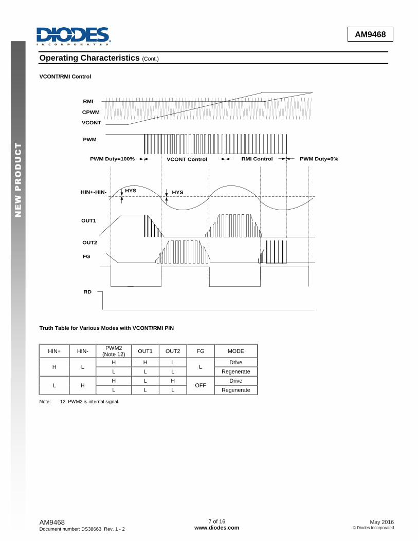
Operating Characteristics (Cont.)
VCONT/RMI Control
Truth Table for Various Modes with VCONT/RMI PIN
Note: 12. PWM2 is internal signal.
HIN+ HIN- PWM2
(Note 12) OUT1 OUT2 FG MODE
H L H H L
L Drive
L L L Regenerate
L H H L H
OFF Drive
L L L Regenerate
PWM
OUT1
OUT2
FG
HIN+-HIN-
RD
VCONT
RMI
CPWM
HYS HYS
PWM Duty=100% VCONT Control RMI Control PWM Duty=0%

AM9468 Document number: DS38663 Rev. 1 - 2
8 of 16 www.diodes.com
May 2016 © Diodes Incorporated
AM9468
NE
W P
RO
DU
CT
Operating Characteristics (Cont.)
Motor Lock
OUT1
OUT2
FG
RD
HIN+- HIN-
Motor Lock Motor Re-roration
tLCK_DET_ON
0.5s (typ)
tOFF
4.5s (typ)
Waiting for
FG Pulse
Motor
Protection
Startup Support 50% Duty
Release
FG Detection

AM9468 Document number: DS38663 Rev. 1 - 2
9 of 16 www.diodes.com
May 2016 © Diodes Incorporated
AM9468
NE
W P
RO
DU
CT
Application Note
HIN-Bias – Hall Bias Output
This is a 1.25V nominal voltage source to bias a differential un-buffered Hall element sensor. If a Hall element requires a lower voltage than the
HIN-Bias output, connect an appropriate value resistor between the HIN-Bias pin and the Hall element supply pin.
HIN+ and HIN- – Hall Inputs
The rotor position is detected by a Hall sensor, with the output of Hall sensor applied to the HIN+ and HIN- pins. This sensor can be either a 4
pin 'naked' Hall device or of the 3 pin buffered switching type. For a 4 pin device the differential Hall output signal is connected to the HIN+ and
HIN- pins. For a buffered Hall sensor the Hall device output is attached to the HIN+ pin, with a pull-up attached if needed, whilst the HIN- pin has
an external potential divider attached to hold the pin at half VREF. When HIN+ is high in relation to HIN-, OUT2 is the active drive.
PWM Pin - External PWM Signal Input for PWM Speed Control Mode
In PWM speed control mode, external PWM signal is applied at this PWM pin to control the motors speed. The duty ratio of the PWM signal input
to this pin controls the fan motor speed by varying the output PWM drive directly.
CPWM Pin
Internal motor control triangular wave is generated based on the capacitor on this pin. A capacitor of 100pF (CPWM = 100pF), will provide a
triangular wave of 36kHz (typ). The VCONT and RMI signals are compared with this triangular wave to generate the speed control PWM drive
and minimum speed control clamp points. The output PWM drive frequency is same as the triangular waveform frequency.
FG/RD Pin
FG is the Frequency Generator (tachometer) output and is a buffered signal from the Hall sensor. RD is the fan locked status detector. FG and
RD are open-drain outputs and will require external pull-up resistors. Typically a pull-up resistor of 10kΩ is recommended from FG and RD pins
to the supply voltage.
RF Pin
The current limiter is activated when the voltage between current detection resistor exceeds 0.25V between GND and RF. The current limiter is
activated at IO = 250mA when RF = 1Ω. The current limit is set with a RF resistor between RF pin and GND pin.
RMI Pin – Minimum Speed Setting Pin
RMI is the minimum speed setting pin. DC voltage on this pin sets minimum speed value; If you do not use RMI (minimum speed control), please
connect it to 5VREG.
VCONT Pin – DC Voltage Speed Control
VCONT is DC voltage inputs speed control pin. The voltage on the VCONT pin is compared with the triangular oscillation on the CPWM pin to
generate the output drive PWM signal. For the control method, refer to the timing chart.
.
REGH/5VREG Pin
Please insert capacitor value 1µF between 5VREG and GND for regulated output voltage stabilization; insert capacitor value 1µF value between
VDD and REGH for stable output voltage.
OUT1 and OUT2 pin
OUT1 and OUT2 pins provide H-bridge driver output for fan and motor coil connection.
VDD – Device Supply Voltage
This provides the supply for the device.
GND – Supply Return
This is the device supply ground return pin for control signal.

AM9468 Document number: DS38663 Rev. 1 - 2
10 of 16 www.diodes.com
May 2016 © Diodes Incorporated
AM9468
NE
W P
RO
DU
CT
Application Note (Cont.)
Speed Control
This device allows both DC voltage input and PWM signal input for speed control. Typically only one of the method is used to control the motor
speed. In DC voltage speed control mode, the voltage on the VCONT pin is compared with the CPWM triangular wave to generate internal PWM
signal to drive the output. In PWM speed control mode, the PWM signal on the PWM pin directly controls the output PWM drive.
The typical application circuits shows the two speed control methods.
1. Speed Control by PWM Pin
REGH
5VREG
VCONT
RMI
FG
RD HIN+
HB
HIN-
CPWM
PWM
GND3
4
5
6
7
8
14
13
12
11
10
9
RF
OUT21
2
16
15
OUT1
Dz
D1 RF
CPWM
Hall
PWM signal for
speed control
C1
SYSTEM
POWER
AM9468
R1
VDD
Motor Coil
2. Speed Control by VCONT/RMI Pin
REGH
5VREG
VCONT
RMI
FG
RD HIN+
HB
HIN-
CPWM
PWM
GND3
4
5
6
7
8
14
13
12
11
10
9
RF
OUT21
2
16
15
OUT1
Dz
D1 RF
CPWM
C1
SYSTEM
POWER
VPWM
Hall
AM9468
R1
VDD
Motor Coil

AM9468 Document number: DS38663 Rev. 1 - 2
11 of 16 www.diodes.com
May 2016 © Diodes Incorporated
AM9468
NE
W P
RO
DU
CT
Typical Operating Characteristics
Average Supply Current
Lock Detect tLCK_DET_ON and Shutdown tOFF Periods
Current Limits
Current Limit (250mV) vs. Temperature
VR
EF
(V
)
VR
EF
(V
)
VREF

AM9468 Document number: DS38663 Rev. 1 - 2
12 of 16 www.diodes.com
May 2016 © Diodes Incorporated
AM9468
NE
W P
RO
DU
CT
Typical Operating Characteristics (Cont.)
AM9468 Total Resistance Total H-Bridge Path Resistance – Total RDS(ON) of High Side and Low Side Switches

AM9468 Document number: DS38663 Rev. 1 - 2
13 of 16 www.diodes.com
May 2016 © Diodes Incorporated
AM9468
NE
W P
RO
DU
CT
Thermal Performance TSSOP-16 Power Dissipation De-rating Curve 1 (Note 13)
TA (C) -40 0 25 50 60 70 80 85 90 95 100 105 110 120 125 130 140 150
PD (mW) 3,520 3,520 3,520 2,816 2,534 2,253 1,971 1,830 1,690 1,549 1,408 1,267 1,126 845 704 563 282 0
Note 13: TSSOP-16 is soldered on FR-4 substrate 4-layer 1.6mm thickness PCB board, calculated in accordance with JESD 51-7.
TSSOP-16 Power Dissipation De-rating Curve 2 (Note 14)
TA (C) -40 0 25 50 60 70 80 85 90 95 100 105 110 120 125 130 140 150
PD (mW) 2,090 2,090 2,090 1,672 1,505 1,338 1,170 1,087 1,003 920 836 752 669 502 418 334 167 0
Note 14: TSSOP-16 is soldered to the circular PCB diameter 1.2” with the center circular cutout diameter of 0.53”. The Hall element space cut-out is 0.12”x0.08”. 2-layer 2oz.copper FR-4 PCB (1.6mm thickness) with partial copper flood on the bottom layer.
TSSOP-16 Thermal Derating Curve
TSSOP-16 Thermal Derating Curve

AM9468 Document number: DS38663 Rev. 1 - 2
14 of 16 www.diodes.com
May 2016 © Diodes Incorporated
AM9468
NE
W P
RO
DU
CT
Thermal Performance Circular PCB Dimensions The circular PCB diameter is 1.2” with the centre circular cut-out diameter of 0.53”. The Hall element space cut-out is 0.12”x0.08”. 2-layer 2oz.copper FR-4 PCB (1.6mm thickness) with partial copper flood on the bottom layer.
Custom Circular PCB – Top View Custom Circular PCB – Bottom View
Ordering Information
AM9468 - X - X
PackingPackage
13 : Tape & ReelT16: TSSOP-16
Product Name
Part Number Package Code Packaging 13” Tape and Reel
Quantity Part Number Suffix
AM9468-T16-13 T16 TSSOP-16 2500/Tape & Reel -13
Marking Information (1) Package Type: TSSOP-16
( Top View )
1
AM9468YY WW X X
Logo
Product Name
8
WW : Week : 01~52; 52
YY : Year : 14,15,16~
X X : Internal Coderepresents 52 and 53 week
16 9

AM9468 Document number: DS38663 Rev. 1 - 2
15 of 16 www.diodes.com
May 2016 © Diodes Incorporated
AM9468
NE
W P
RO
DU
CT
Package Outline Dimensions Please see http://www.diodes.com/package-outlines.html for the latest version.
(1) Package Type: TSSOP-16
Ø0.760Depth0.050±0.02
R1
x)
C
DETAIL 'A'
PIN 1
e b
E
E/2
E1
A2
A
D
A1
X
Y SEE DETAIL 'A'
SEATING PLANE
GAUGE
PLANE
R
L
L1
L2
TSSOP-16
Dim Min Max Typ
A - 1.08 -
A1 0.05 0.15 -
A2 0.80 0.93 -
b 0.19 0.30 -
c 0.09 0.20 -
D 4.90 5.10 -
E 6.40 BSC
E1 4.30 4.50 -
e 0.65 BSC
L 0.45 0.75 -
L1 1.00 REF
L2 0.25 BSC
R / R1 0.09 - -
X - - 1.350
Y - - 1.050
θ 0° 8° -
θ1 5° 15° -
θ2 0° - -
All Dimensions in mm
Suggested Pad Layout Please see http://www.diodes.com/package-outlines.html for the latest version. (1) Package Type: TSSOP-16
X1
Y
Y1
X
1
C
Dimensions Value
(in mm)
C 0.650
X 0.350
X1 4.900
Y 1.400
Y1 6.800
AM9468 Document number: DS38663 Rev. 1 - 2
16 of 16 www.diodes.com
May 2016 © Diodes Incorporated
AM9468
NE
W P
RO
DU
CT
IMPORTANT NOTICE DIODES INCORPORATED MAKES NO WARRANTY OF ANY KIND, EXPRESS OR IMPLIED, WITH REGARDS TO THIS DOCUMENT, INCLUDING, BUT NOT LIMITED TO, THE IMPLIED WARRANTIES OF MERCHANTABILITY AND FITNESS FOR A PARTICULAR PURPOSE (AND THEIR EQUIVALENTS UNDER THE LAWS OF ANY JURISDICTION). Diodes Incorporated and its subsidiaries reserve the right to make modifications, enhancements, improvements, corrections or other changes without further notice to this document and any product described herein. Diodes Incorporated does not assume any liability arising out of the application or use of this document or any product described herein; neither does Diodes Incorporated convey any license under its patent or trademark rights, nor the rights of others. Any Customer or user of this document or products described herein in such applications shall assume all risks of such use and will agree to hold Diodes Incorporated and all the companies whose products are represented on Diodes Incorporated website, harmless against all damages. Diodes Incorporated does not warrant or accept any liability whatsoever in respect of any products purchased through unauthorized sales channel. Should Customers purchase or use Diodes Incorporated products for any unintended or unauthorized application, Customers shall indemnify and hold Diodes Incorporated and its representatives harmless against all claims, damages, expenses, and attorney fees arising out of, directly or indirectly, any claim of personal injury or death associated with such unintended or unauthorized application. Products described herein may be covered by one or more United States, international or foreign patents pending. Product names and markings noted herein may also be covered by one or more United States, international or foreign trademarks. This document is written in English but may be translated into multiple languages for reference. Only the English version of this document is the final and determinative format released by Diodes Incorporated.
LIFE SUPPORT Diodes Incorporated products are specifically not authorized for use as critical components in life support devices or systems without the express written approval of the Chief Executive Officer of Diodes Incorporated. As used herein: A. Life support devices or systems are devices or systems which: 1. are intended to implant into the body, or
2. support or sustain life and whose failure to perform when properly used in accordance with instructions for use provided in the labeling can be reasonably expected to result in significant injury to the user.
B. A critical component is any component in a life support device or system whose failure to perform can be reasonably expected to cause the failure of the life support device or to affect its safety or effectiveness. Customers represent that they have all necessary expertise in the safety and regulatory ramifications of their life support devices or systems, and acknowledge and agree that they are solely responsible for all legal, regulatory and safety-related requirements concerning their products and any use of Diodes Incorporated products in such safety-critical, life support devices or systems, notwithstanding any devices- or systems-related information or support that may be provided by Diodes Incorporated. Further, Customers must fully indemnify Diodes Incorporated and its representatives against any damages arising out of the use of Diodes Incorporated products in such safety-critical, life support devices or systems. Copyright © 2016, Diodes Incorporated www.diodes.com