
RL78/G13 Data sheet - RS Components...
127
Datasheet RL78/G13 RENESAS MCU True Low Power Platform (as low as 66 μA/MHz, and 0.57 μA for RTC + LVD), 1.6 V to 5.5 V operation, 16 to 512 Kbyte Flash, 41 DMIPS at 32 MHz, for General Purpose Applications Page 1 of 124 R01DS0131EJ0200 Rev.2.00 Oct 12, 2012 R01DS0131EJ0200 Rev.2.00 Oct 12, 2012 1. OUTLINE 1.1 Features Ultra-Low Power Technology • 1.6 V to 5.5 V operation from a single supply • Stop (RAM retained): 0.23 μA, (LVD enabled): 0.31 μA • Halt (RTC + LVD): 0.57 μA • Snooze: 0.70 mA (UART), 1.20 mA (ADC) • Operating: 66 μA/MHz 16-bit RL78 CPU Core • Delivers 41 DMIPS at maximum operating frequency of 32 MHz • Instruction Execution: 86% of instructions can be executed in 1 to 2 clock cycles • CISC Architecture (Harvard) with 3-stage pipeline • Multiply Signed & Unsigned: 16 x 16 to 32-bit result in 1 clock cycle • MAC: 16 x 16 to 32-bit result in 2 clock cycles • 16-bit barrel shifter for shift & rotate in 1 clock cycle • 1-wire on-chip debug function Main Flash Memory • Density: 16 KB to 512 KB • Block size: 1 KB • On-chip single voltage flash memory with protection from block erase/writing • Self-programming with secure boot swap function and flash shield window function Data Flash Memory • Data Flash with background operation • Data flash size: 4 KB to 8 KB size options • Erase Cycles: 1 Million (typ.) • Erase/programming voltage: 1.8 V to 5.5 V RAM • 2 KB to 32 KB size options • Supports operands or instructions • Back-up retention in all modes High-speed On-chip Oscillator • 32 MHz with +/− 1% accuracy over voltage (1.8 V to 5.5 V) and temperature (−20 °C to 85 °C) • Pre-configured settings: 32 MHz, 24 MHz, 16 MHz, 12 MHz, 8 MHz, 4 MHz & 1 MHz Reset and Supply Management • Power-on reset (POR) monitor/generator • Low voltage detection (LVD) with 14 setting options (Interrupt and/or reset function) Data Memory Access (DMA) Controller • Up to 4 fully programmable channels • Transfer unit: 8- or 16-bit Multiple Communication Interfaces • Up to 8 x I 2 C master • Up to 2 x I 2 C multi-master • Up to 8 x CSI/SPI (7-, 8-bit) • Up to 4 x UART (7-, 8-, 9-bit) • Up to 1 x LIN Extended-Function Timers • Multi-function 16-bit timers: Up to 16 channels • Real-time clock (RTC): 1 channel (full calendar and alarm function with watch correction function) • Interval Timer: 12-bit, 1 channel • 15 kHz watchdog timer : 1 channel (window function) Rich Analog • ADC: Up to 26 channels, 10-bit resolution, 2.1 μs conversion time • Supports 1.6 V • Internal voltage reference (1.45 V) • On-chip temperature sensor Safety Features (IEC or UL 60730 compliance) • Flash memory CRC calculation • RAM parity error check • RAM write protection • SFR write protection • Illegal memory access detection • Clock stop/ frequency detection • ADC self-test General Purpose I/O • 5V tolerant, high-current (up to 20 mA per pin) • Open-Drain, Internal Pull-up support Operating Ambient Temperature • Standard: −40 °C to +85 °C • Extended: −40 °C to +105 °C Package Type and Pin Count From 3mm x 3mm to 14mm x 20mm QFP: 44, 48, 52, 64, 80, 100, 128 QFN: 24, 32, 40, 48 SSOP: 20, 30 LGA: 25, 36 BGA: 64
Transcript of RL78/G13 Data sheet - RS Components...

Datasheet
RL78/G13
RENESAS MCU
True Low Power Platform (as low as 66 µA/MHz, and 0.57 µA for RTC + LVD), 1.6 V to 5.5 V operation, 16 to 512 Kbyte Flash, 41 DMIPS at 32 MHz, for General Purpose Applications
Page 1 of 124
R01DS0131EJ0200Rev.2.00
Oct 12, 2012
R01DS0131EJ0200 Rev.2.00 Oct 12, 2012
1. OUTLINE
1.1 Features
Ultra-Low Power Technology • 1.6 V to 5.5 V operation from a single supply • Stop (RAM retained): 0.23 µA, (LVD enabled): 0.31
µA • Halt (RTC + LVD): 0.57 µA • Snooze: 0.70 mA (UART), 1.20 mA (ADC) • Operating: 66 µA/MHz
16-bit RL78 CPU Core • Delivers 41 DMIPS at maximum operating frequency
of 32 MHz • Instruction Execution: 86% of instructions can be
executed in 1 to 2 clock cycles • CISC Architecture (Harvard) with 3-stage pipeline • Multiply Signed & Unsigned: 16 x 16 to 32-bit result in
1 clock cycle • MAC: 16 x 16 to 32-bit result in 2 clock cycles • 16-bit barrel shifter for shift & rotate in 1 clock cycle • 1-wire on-chip debug function
Main Flash Memory • Density: 16 KB to 512 KB • Block size: 1 KB • On-chip single voltage flash memory with protection
from block erase/writing • Self-programming with secure boot swap function
and flash shield window function
Data Flash Memory • Data Flash with background operation • Data flash size: 4 KB to 8 KB size options • Erase Cycles: 1 Million (typ.) • Erase/programming voltage: 1.8 V to 5.5 V
RAM • 2 KB to 32 KB size options • Supports operands or instructions • Back-up retention in all modes
High-speed On-chip Oscillator • 32 MHz with +/− 1% accuracy over voltage (1.8 V to
5.5 V) and temperature (−20 °C to 85 °C) • Pre-configured settings: 32 MHz, 24 MHz, 16 MHz,
12 MHz, 8 MHz, 4 MHz & 1 MHz
Reset and Supply Management • Power-on reset (POR) monitor/generator • Low voltage detection (LVD) with 14 setting options
(Interrupt and/or reset function)
Data Memory Access (DMA) Controller • Up to 4 fully programmable channels • Transfer unit: 8- or 16-bit
Multiple Communication Interfaces • Up to 8 x I2C master • Up to 2 x I2C multi-master • Up to 8 x CSI/SPI (7-, 8-bit) • Up to 4 x UART (7-, 8-, 9-bit) • Up to 1 x LIN
Extended-Function Timers • Multi-function 16-bit timers: Up to 16 channels • Real-time clock (RTC): 1 channel (full calendar and
alarm function with watch correction function) • Interval Timer: 12-bit, 1 channel • 15 kHz watchdog timer : 1 channel (window function)
Rich Analog • ADC: Up to 26 channels, 10-bit resolution, 2.1 µs
conversion time • Supports 1.6 V • Internal voltage reference (1.45 V) • On-chip temperature sensor
Safety Features (IEC or UL 60730 compliance) • Flash memory CRC calculation • RAM parity error check • RAM write protection • SFR write protection • Illegal memory access detection • Clock stop/ frequency detection • ADC self-test
General Purpose I/O • 5V tolerant, high-current (up to 20 mA per pin) • Open-Drain, Internal Pull-up support
Operating Ambient Temperature • Standard: −40 °C to +85 °C • Extended: −40 °C to +105 °C
Package Type and Pin Count From 3mm x 3mm to 14mm x 20mm QFP: 44, 48, 52, 64, 80, 100, 128 QFN: 24, 32, 40, 48 SSOP: 20, 30 LGA: 25, 36 BGA: 64
RL78/G13 CHAPTER 1 OUTLINE
Page 2 of 124R01DS0131EJ0200 Rev.2.00 Oct 12, 2012
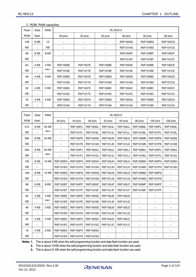
ROM, RAM capacities
RL78/G13 Flash
ROM
Data
flash
RAM
20 pins 24 pins 25 pins 30 pins 32 pins 36 pins
8 KB − − − R5F100AG R5F100BG R5F100CG 128
KB −
12
KB − − − R5F101AG R5F101BG R5F101CG
8 KB − − − R5F100AF R5F100BF R5F100CF 96
KB −
8 KB
− − − R5F101AF R5F101BF R5F101CF
4 KB R5F1006E R5F1007E R5F1008E R5F100AE R5F100BE R5F100CE 64
KB −
4 KB
Note 1 R5F1016E R5F1017E R5F1018E R5F101AE R5F101BE R5F101CE
4 KB R5F1006D R5F1007D R5F1008D R5F100AD R5F100BD R5F100CD 48
KB −
3 KB
R5F1016D R5F1017D R5F1018D R5F101AD R5F101BD R5F101CD
4 KB R5F1006C R5F1007C R5F1008C R5F100AC R5F100BC R5F100CC 32
KB −
2 KB
R5F1016C R5F1017C R5F1018C R5F101AC R5F101BC R5F101CC
4 KB R5F1006A R5F1007A R5F1008A R5F100AA R5F100BA R5F100CA 16
KB −
2 KB
R5F1016A R5F1017A R5F1018A R5F101AA R5F101BA R5F101CA
RL78/G13 Flash
ROM
Data
flash
RAM
40 pins 44 pins 48 pins 52 pins 64 pins 80 pins 100 pins 128 pins
8 KB − R5F100FL R5F100GL R5F100JL R5F100LL R5F100ML R5F100PL R5F100SL512
KB −
32 KB
Note 3 − R5F101FL R5F101GL R5F101JL R5F101LL R5F101ML R5F101PL R5F101SL
8 KB − R5F100FK R5F100GK R5F100JK R5F100LK R5F100MK R5F100PK R5F100SK384
KB −
24 KB
− R5F101FK R5F101GK R5F101JK R5F101LK R5F101MK R5F101PK R5F101SK
8 KB − R5F100FJ R5F100GJ R5F100JJ R5F100LJ R5F100MJ R5F100PJ R5F100SJ256
KB −
20 KB
Note 2 − R5F101FJ R5F101GJ R5F101JJ R5F101LJ R5F101MJ R5F101PJ R5F101SJ
8 KB R5F100EH R5F100FH R5F100GH R5F100JH R5F100LH R5F100MH R5F100PH R5F100SH192
KB −
16 KB
R5F101EH R5F101FH R5F101GH R5F101JH R5F101LH R5F101MH R5F101PH R5F101SH
8 KB R5F100EG R5F100FG R5F100GG R5F100JG R5F100LG R5F100MG R5F100PG − 128
KB −
12 KB
R5F101EG R5F101FG R5F101GG R5F101JG R5F101LG R5F101MG R5F101PG −
8 KB R5F100EF R5F100FF R5F100GF R5F100JF R5F100LF R5F100MF R5F100PF − 96
KB −
8 KB
R5F101EF R5F101FF R5F101GF R5F101JF R5F101LF R5F101MF R5F101PF −
4 KB R5F100EE R5F100FE R5F100GE R5F100JE R5F100LE − − − 64
KB −
4 KB
Note 1 R5F101EE R5F101FE R5F101GE R5F101JE R5F101LE − − −
4 KB R5F100ED R5F100FD R5F100GD R5F100JD R5F100LD − − − 48
KB −
3 KB
R5F101ED R5F101FD R5F101GD R5F101JD R5F101LD − − −
4 KB R5F100EC R5F100FC R5F100GC R5F100JC R5F100LC − − − 32
KB −
2 KB
R5F101EC R5F101FC R5F101GC R5F101JC R5F101LC − − −
4 KB R5F100EA R5F100FA R5F100GA − − − − − 16
KB −
2 KB
R5F101EA R5F101FA R5F101GA − − − − −
Notes 1. This is about 3 KB when the self-programming function and data flash function are used. 2. This is about 19 KB when the self-programming function and data flash function are used. 3. This is about 31 KB when the self-programming function and data flash function are used.

RL78/G13 CHAPTER 1 OUTLINE
Page 3 of 124R01DS0131EJ0200 Rev.2.00 Oct 12, 2012
1.2 Ordering Information
• Flash memory version (lead-free product)
(1/4)
Pin count Package Data flash Part Number
Mounted R5F1006AASP, R5F1006CASP, R5F1006DASP, R5F1006EASP
R5F1006ADSP, R5F1006CDSP, R5F1006DDSP, R5F1006EDSP
20 pins 20-pin plastic SSOP
(7.62 mm (300))
Not mounted R5F1016AASP, R5F1016CASP, R5F1016DASP, R5F1016EASP
R5F1016ADSP, R5F1016CDSP, R5F1016DDSP, R5F1016EDSP
Mounted R5F1007AANA, R5F1007CANA, R5F1007DANA, R5F1007EANA
R5F1007ADNA, R5F1007CDNA, R5F1007DDNA, R5F1007EDNA
24 pins 24-pin plastic WQFN
(fine pitch) (4 × 4)
Not mounted R5F1017AANA, R5F1017CANA, R5F1017DANA, R5F1017EANA
R5F1017ADNA, R5F1017CDNA, R5F1017DDNA, R5F1017EDNA
Mounted R5F1008AALA, R5F1008CALA, R5F1008DALA, R5F1008EALA
R5F1008ADLA, R5F1008CDLA, R5F1008DDLA, R5F1008EDLA 25 pins 25-pin plastic FLGA
(3 × 3)
Not mounted R5F1018AALA, R5F1018CALA, R5F1018DALA, R5F1018EALA
R5F1018ADLA, R5F1018CDLA, R5F1018DDLA, R5F1018EDLA
Mounted R5F100AAASP, R5F100ACASP, R5F100ADASP,
R5F100AEASP, R5F100AFASP, R5F100AGASP
R5F100AADSP, R5F100ACDSP, R5F100ADDSP, R5F100AEDSP,
R5F100AFDSP, R5F100AGDSP
30 pins 30-pin plastic SSOP
(7.62 mm (300))
Not mounted R5F101AAASP, R5F101ACASP, R5F101ADASP,
R5F101AEASP, R5F101AFASP, R5F101AGASP
R5F101AADSP, R5F101ACDSP, R5F101ADDSP, R5F101AEDSP,
R5F101AFDSP, R5F101AGDSP
Mounted R5F100BAANA, R5F100BCANA, R5F100BDANA, R5F100BEANA,
R5F100BFANA, R5F100BGANA
R5F100BADNA, R5F100BCDNA, R5F100BDDNA,
R5F100BEDNA, R5F100BFDNA, R5F100BGDNA
32 pins 32-pin plastic WQFN
(fine pitch)(5 × 5)
Not mounted R5F101BAANA, R5F101BCANA, R5F101BDANA, R5F101BEANA,
R5F101BFANA, R5F101BGANA
R5F101BADNA, R5F101BCDNA, R5F101BDDNA,
R5F101BEDNA, R5F101BFDNA, R5F101BGDNA
Mounted R5F100CAALA, R5F100CCALA, R5F100CDALA, R5F100CEALA,
R5F100CFALA, R5F100CGALA
R5F100CADLA, R5F100CCDLA, R5F100CDDLA, R5F100CEDLA,
R5F100CFDLA, R5F100CGDLA
36 pins 36-pin plastic FLGA
(4 × 4)
Not mounted R5F101CAALA, R5F101CCALA, R5F101CDALA, R5F101CEALA,
R5F101CFALA, R5F101CGALA
R5F101CADLA, R5F101CCDLA, R5F101CDDLA, R5F101CEDLA,
R5F101CFDLA, R5F101CGDLA

RL78/G13 CHAPTER 1 OUTLINE
Page 4 of 124R01DS0131EJ0200 Rev.2.00 Oct 12, 2012
(2/4)
Pin count Package Data flash Part Number
Mounted R5F100EAANA, R5F100ECANA, R5F100EDANA, R5F100EEANA,
R5F100EFANA, R5F100EGANA, R5F100EHANA
R5F100EADNA, R5F100ECDNA, R5F100EDDNA, R5F100EEDNA,
R5F100EFDNA, R5F100EGDNA, R5F100EHDNA
40 pins 40-pin plastic WQFN
(fine pitch)(6 × 6)
Not mounted R5F101EAANA, R5F101ECANA, R5F101EDANA, R5F101EEANA,
R5F101EFANA, R5F101EGANA, R5F101EHANA
R5F101EADNA, R5F101ECDNA, R5F101EDDNA, R5F101EEDNA,
R5F101EFDNA, R5F101EGDNA, R5F101EHDNA
Mounted R5F100FAAFP, R5F100FCAFP, R5F100FDAFP, R5F100FEAFP,
R5F100FFAFP, R5F100FGAFP, R5F100FHAFP, R5F100FJAFP,
R5F100FKAFP, R5F100FLAFP
R5F100FADFP, R5F100FCDFP, R5F100FDDFP, R5F100FEDFP,
R5F100FFDFP, R5F100FGDFP, R5F100FHDFP, R5F100FJDFP,
R5F100FKDFP, R5F100FLDFP
44 pins 44-pin plastic LQFP
(10 × 10)
Not mounted R5F101FAAFP, R5F101FCAFP, R5F101FDAFP, R5F101FEAFP,
R5F101FFAFP, R5F101FGAFP, R5F101FHAFP, R5F101FJAFP,
R5F101FKAFP, R5F101FLAFP
R5F101FADFP, R5F101FCDFP, R5F101FDDFP, R5F101FEDFP,
R5F101FFDFP, R5F101FGDFP, R5F101FHDFP, R5F101FJDFP,
R5F101FKDFP, R5F101FLDFP
Mounted R5F100GAAFB, R5F100GCAFB, R5F100GDAFB, R5F100GEAFB,
R5F100GFAFB, R5F100GGAFB, R5F100GHAFB, R5F100GJAFB,
R5F100GKAFB, R5F100GLAFB
R5F100GADFB, R5F100GCDFB, R5F100GDDFB, R5F100GEDFB,
R5F100GFDFB, R5F100GGDFB, R5F100GHDFB, R5F100GJDFB,
R5F100GKDFB, R5F100GLDFB
48-pin plastic LQFP
(fine pitch) (7 × 7)
Not mounted R5F101GAAFB, R5F101GCAFB, R5F101GDAFB, R5F101GEAFB,
R5F101GFAFB, R5F101GGAFB, R5F101GHAFB, R5F101GJAFB,
R5F101GKAFB, R5F101GLAFB
R5F101GADFB, R5F101GCDFB, R5F101GDDFB, R5F101GEDFB,
R5F101GFDFB, R5F101GGDFB, R5F101GHDFB, R5F101GJDFB,
R5F101GKDFB, R5F101GLDFB
Mounted R5F100GAANA, R5F100GCANA, R5F100GDANA, R5F100GEANA,
R5F100GFANA, R5F100GGANA, R5F100GHANA, R5F100GJANA,
R5F100GKANA, R5F100GLANA
R5F100GADNA, R5F100GCDNA, R5F100GDDNA, R5F100GEDNA,
R5F100GFDNA, R5F100GGDNA, R5F100GHDNA, R5F100GJDNA,
R5F100GKDNA, R5F100GLDNA
48 pins
48-pin plastic WQFN
(7 × 7)
Not mounted R5F101GAANA, R5F101GCANA, R5F101GDANA, R5F101GEANA,
R5F101GFANA, R5F101GGANA, R5F101GHANA, R5F101GJANA,
R5F101GKANA, R5F101GLANA
R5F101GADNA, R5F101GCDNA, R5F101GDDNA, R5F101GEDNA,
R5F101GFDNA, R5F101GGDNA, R5F101GHDNA, R5F101GJDNA,
R5F101GKDNA, R5F101GLDNA

RL78/G13 CHAPTER 1 OUTLINE
Page 5 of 124R01DS0131EJ0200 Rev.2.00 Oct 12, 2012
(3/4)
Pin count Package Data flash Part Number
Mounted R5F100JCAFA, R5F100JDAFA, R5F100JEAFA, R5F100JFAFA,
R5F100JGAFA, R5F100JHAFA, R5F100JJAFA, R5F100JKAFA,
R5F100JLAFA
R5F100JCDFA, R5F100JDDFA, R5F100JEDFA, R5F100JFDFA,
R5F100JGDFA, R5F100JHDFA, R5F100JJDFA, R5F100JKDFA,
R5F100JLDFA
52 pins 52-pin plastic LQFP
(10 × 10)
Not mounted R5F101JCAFA, R5F101JDAFA, R5F101JEAFA, R5F101JFAFA,
R5F101JGAFA, R5F101JHAFA, R5F101JJAFA, R5F101JKAFA,
R5F101JLAFA
R5F101JCDFA, R5F101JDDFA, R5F101JEDFA, R5F101JFDFA,
R5F101JGDFA, R5F101JHDFA, R5F101JJDFA, R5F101JKDFA,
R5F101JLDFA
Mounted R5F100LCAFA, R5F100LDAFA, R5F100LEAFA, R5F100LFAFA,
R5F100LGAFA, R5F100LHAFA, R5F100LJAFA, R5F100LKAFA,
R5F100LLAFA
R5F100LCDFA, R5F100LDDFA, R5F100LEDFA, R5F100LFDFA,
R5F100LGDFA, R5F100LHDFA, R5F100LJDFA, R5F100LKDFA,
R5F100LLDFA
64-pin plastic LQFP
(12 × 12)
Not mounted R5F101LCAFA, R5F101LDAFA, R5F101LEAFA, R5F101LFAFA,
R5F101LGAFA, R5F101LHAFA, R5F101LJAFA, R5F101LKAFA,
R5F101LLAFA
R5F101LCDFA, R5F101LDDFA, R5F101LEDFA, R5F101LFDFA,
R5F101LGDFA, R5F101LHDFA, R5F101LJDFA, R5F101LKDFA,
R5F101LLDFA
Mounted R5F100LCAFB, R5F100LDAFB, R5F100LEAFB, R5F100LFAFB,
R5F100LGAFB, R5F100LHAFB, R5F100LJAFB, R5F100LKAFB,
R5F100LLAFB
R5F100LCDFB, R5F100LDDFB, R5F100LEDFB, R5F100LFDFB,
R5F100LGDFB, R5F100LHDFB, R5F100LJDFB, R5F100LKDFB,
R5F100LLDFB
64-pin plastic LQFP
(fine pitch) (10 × 10)
Not mounted R5F101LCAFB, R5F101LDAFB, R5F101LEAFB, R5F101LFAFB,
R5F101LGAFB, R5F101LHAFB, R5F101LJAFB, R5F101LKAFB,
R5F101LLAFB
R5F101LCDFB, R5F101LDDFB, R5F101LEDFB, R5F101LFDFB,
R5F101LGDFB, R5F101LHDFB, R5F101LJDFB, R5F101LKDFB,
R5F101LLDFB
Mounted R5F100LCABG, R5F100LDABG, R5F100LEABG, R5F100LFABG,
R5F100LGABG, R5F100LHABG, R5F100LJABG
R5F100LCDBG, R5F100LDDBG, R5F100LEDBG, R5F100LFDBG,
R5F100LGDBG, R5F100LHDBG, R5F100LJDBG
64 pins
64-pin plastic FBGA
(4 × 4)
Not mounted R5F101LCABG, R5F101LDABG, R5F101LEABG, R5F101LFABG,
R5F101LGABG, R5F101LHABG, R5F101LJABG
R5F101LCDBG, R5F101LDDBG, R5F101LEDBG, R5F101LFDBG,
R5F101LGDBG, R5F101LHDBG, R5F101LJDBG

RL78/G13 CHAPTER 1 OUTLINE
Page 6 of 124R01DS0131EJ0200 Rev.2.00 Oct 12, 2012
(4/4)
Pin count Package Data flash Part Number
Mounted R5F100MFAFA, R5F100MGAFA, R5F100MHAFA, R5F100MJAFA,
R5F100MKAFA, R5F100MLAFA
R5F100MFDFA, R5F100MGDFA, R5F100MHDFA,
R5F100MJDFA, R5F100MKDFA, R5F100MLDFA
80-pin plastic LQFP
(14 × 14)
Not mounted R5F101MFAFA, R5F101MGAFA, R5F101MHAFA, R5F101MJAFA,
R5F101MKAFA, R5F101MLAFA
R5F101MFDFA, R5F101MGDFA, R5F101MHDFA,
R5F101MJDFA, R5F101MKDFA, R5F101MLDFA
Mounted R5F100MFAFB, R5F100MGAFB, R5F100MHAFB, R5F100MJAFB,
R5F100MKAFB, R5F100MLAFB
R5F100MFDFB, R5F100MGDFB, R5F100MHDFB,
R5F100MJDFB, R5F100MKDFB, R5F100MLDFB
80 pins
80-pin plastic LQFP
(fine pitch) (12 × 12)
Not mounted R5F101MFAFB, R5F101MGAFB, R5F101MHAFB, R5F101MJAFB,
R5F101MKAFB, R5F101MLAFB
R5F101MFDFB, R5F101MGDFB, R5F101MHDFB,
R5F101MJDFB, R5F101MKDFB, R5F101MLDFB
Mounted R5F100PFAFB, R5F100PGAFB, R5F100PHAFB, R5F100PJAFB,
R5F100PKAFB, R5F100PLAFB
R5F100PFDFB, R5F100PGDFB, R5F100PHDFB, R5F100PJDFB,
R5F100PKDFB, R5F100PLDFB
100-pin plastic LQFP
(fine pitch) (14 × 14)
Not mounted R5F101PFAFB, R5F101PGAFB, R5F101PHAFB, R5F101PJAFB,
R5F101PKAFB, R5F101PLAFB
R5F101PFDFB, R5F101PGDFB, R5F101PHDFB, R5F101PJDFB,
R5F101PKDFB, R5F101PLDFB
Mounted R5F100PFAFA, R5F100PGAFA, R5F100PHAFA, R5F100PJAFA,
R5F100PKAFA, R5F100PLAFA
R5F100PFDFA, R5F100PGDFA, R5F100PHDFA, R5F100PJDFA,
R5F100PKDFA, R5F100PLDFA
100 pins
100-pin plastic LQFP
(14 × 20)
Not mounted R5F101PFAFA, R5F101PGAFA, R5F101PHAFA, R5F101PJAFA,
R5F101PKAFA, R5F101PLAFA
R5F101PFDFA, R5F101PGDFA, R5F101PHDFA, R5F101PJDFA,
R5F101PKDFA, R5F101PLDFA
Mounted R5F100SHAFB, R5F100SJAFB, R5F100SKAFB, R5F100SLAFB
R5F100SHDFB, R5F100SJDFB, R5F100SKDFB, R5F100SLDFB
128 pins 128-pin plastic LQFP
(fine pitch) (14 × 20)
Not mounted R5F101SHAFB, R5F101SJAFB, R5F101SKAFB, R5F101SLAFB
R5F101SHDFB, R5F101SJDFB, R5F101SKDFB, R5F101SLDFB

RL78/G13 CHAPTER 1 OUTLINE
Page 7 of 124R01DS0131EJ0200 Rev.2.00 Oct 12, 2012
Figure 1-1. Part Number, Memory Size, and Package of RL78/G13
Part No. R 5 F 1 0 0 L E A x x x F B
Package type:
ROM number (Omitted with blank products)
ROM capacity:
RL78/G13 group
Renesas MCU
Renesas semiconductor product
SP : SSOP, 0.65 mm pitchFP : LQFP, 0.80 mm pitchFA : LQFP, 0.65 mm pitchFB : LQFP, 0.50 mm pitchNA : WQFN, 0.50 mm pitchLA : LGA, 0.50 mm pitchBG : FBGA, 0.40 mm pitch
A : 16 KBC : 32 KBD : 48 KBE : 64 KBF : 96 KBG : 128 KBH : 192 KBJ : 256 KBK : 384 KBL : 512 KB
Pin count:6 : 20-pin7 : 24-pin8 : 25-pinA : 30-pinB : 32-pinC : 36-pinE : 40-pinF : 44-pinG : 48-pinJ : 52-pinL : 64-pinM : 80-pinP : 100-pinS : 128-pin
Classification:A : Consumer applications, operating ambient temperature : -40˚C to 85˚CD : Industrial applications, operating ambient temperature : -40˚C to 85˚C
Memory type:F : Flash memory
100 : Data flash is provided101 : Data flash is not provided
Remark For details about extended-temperature products (operating ambient temperature: −40°C to 105°C),
contact a Renesas Electronics Corporation or an authorized Renesas Electronics Corporation
distributor.
<R>

RL78/G13 CHAPTER 1 OUTLINE
Page 8 of 124R01DS0131EJ0200 Rev.2.00 Oct 12, 2012
1.3 Pin Configuration (Top View)
1.3.1 20-pin products
• 20-pin plastic SSOP (7.62 mm (300))
20191817161514131211
12345678910
P20/ANI0/AVREFP
P21/ANI1/AVREFM
P22/ANI2P147/ANI18P10/SCK00/SCL00P11/SI00/RxD0/TOOLRxD/SDA00P12/SO00/TxD0/TOOLTxDP16/TI01/TO01/INTP5/SO11P17/TI02/TO02/SI11/SDA11P30/INTP3/SCK11/SCL11
P01/ANI16/TO00/RxD1 P00/ANI17/TI00/TxD1
P40/TOOL0 RESET
P137/INTP0 P122/X2/EXCLK
P121/X1 REGC
VSS
VDD
Caution Connect the REGC pin to Vss via a capacitor (0.47 to 1 μF).
Remark For pin identification, see 1.4 Pin Identification.

RL78/G13 CHAPTER 1 OUTLINE
Page 9 of 124R01DS0131EJ0200 Rev.2.00 Oct 12, 2012
1.3.2 24-pin products
• 24-pin plastic WQFN (fine pitch) (4 × 4)
121110
987
192021222324
18 17 16 15 14 13
1 2 3 4 5 6
P21/ANI1/AVREFM
P20/ANI0/AVREFP
P01/ANI16/TO00/RxD1P00/ANI17/TI00/TxD1
P40/TOOL0RESET
exposed die padP
22/A
NI2
P14
7/A
NI1
8P
10/S
CK
00/S
CL0
0P
11/S
I00/
RxD
0/T
OO
LRxD
/SD
A00
P12
/SO
00/T
xD0/
TO
OLT
xDP
16/T
I01/
TO
01/IN
TP
5
P13
7/IN
TP
0P
122/
X2/
EX
CLK
P12
1/X
1R
EG
CV
SS
VD
D
P17/TI02/TO02/SO11P50/INTP1/SI11/SDA11P30/INTP3/SCK11/SCL11P31/TI03/TO03/INTP4/PCLBUZ0P61/SDAA0P60/SCLA0
Caution Connect the REGC pin to Vss via a capacitor (0.47 to 1 μF).
Remark For pin identification, see 1.4 Pin Identification.

RL78/G13 CHAPTER 1 OUTLINE
Page 10 of 124R01DS0131EJ0200 Rev.2.00 Oct 12, 2012
1.3.3 25-pin products
• 25-pin plastic FLGA (3 × 3)
INDEX MARK
Top View Bottom View
5
4
3
2
1
A B C D E E D C B A
INDEX MARK
A B C D E
5
P40/TOOL0
RESET
P01/ANI16/ TO00/RxD1
P22/ANI2
P147/ANI18 5
4
P122/X2/ EXCLK
P137/INTP0
P00/ANI17/ TI00/TxD1
P21/ANI1/ AVREFM
P10/SCK00/ SCL00
4
3
P121/X1
VDD
P20/ANI0/ AVREFP
P12/SO00/ TxD0/ TOOLTxD
P11/SI00/ RxD0/ TOOLRxD/ SDA00
3
2
REGC
VSS
P30/INTP3/ SCK11/SCL11
P17/TI02/ TO02/SO11
P50/INTP1/ SI11/SDA11
2
1
P60/SCLA0
P61/SDAA0
P31/TI03/ TO03/INTP4/ PCLBUZ0
P16/TI01/ TO01/INTP5
P130
1
A B C D E
Caution Connect the REGC pin to Vss via a capacitor (0.47 to 1 μF).
Remark For pin identification, see 1.4 Pin Identification.

RL78/G13 CHAPTER 1 OUTLINE
Page 11 of 124R01DS0131EJ0200 Rev.2.00 Oct 12, 2012
1.3.4 30-pin products
• 30-pin plastic SSOP (7.62 mm (300))
302928272625242322212019181716
123456789101112131415
P21/ANI1/AVREFM
P22/ANI2P23/ANI3P147/ANI18P10/SCK00/SCL00/(TI07)/(TO07)P11/SI00/RxD0/TOOLRxD/SDA00/(TI06)/(TO06)P12/SO00/TxD0/TOOLTxD/(TI05)/(TO05)P13/TxD2/SO20/(SDAA0)/(TI04)/(TO04)P14/RxD2/SI20/SDA20/(SCLA0)/(TI03)/(TO03)P15/PCLBUZ1/SCK20/SCL20/(TI02)/(TO02)P16/TI01/TO01/INTP5/(RXD0)P17/TI02/TO02/(TXD0)P51/INTP2/SO11P50/INTP1/SI11/SDA11P30/INTP3/SCK11/SCL11
P20/ANI0/AVREFP P01/ANI16/TO00/RxD1
P00/ANI17/TI00/TxD1 P120/ANI19 P40/TOOL0
RESET P137/INTP0
P122/X2/EXCLK P121/X1
REGC VSS
VDD
P60/SCLA0 P61/SDAA0
P31/TI03/TO03/INTP4/PCLBUZ0
Caution Connect the REGC pin to Vss via a capacitor (0.47 to 1 μF).
Remarks 1. For pin identification, see 1.4 Pin Identification.
2. Functions in parentheses in the above figure can be assigned via settings in the peripheral I/O
redirection register (PIOR).

RL78/G13 CHAPTER 1 OUTLINE
Page 12 of 124R01DS0131EJ0200 Rev.2.00 Oct 12, 2012
1.3.5 32-pin products
• 32-pin plastic WQFN (5 × 5)
16151413121110
9
2526272829303132
24 23 22 21 20 19 18 17
1 2 3 4 5 6 7 8
P147/ANI18P23/ANI3P22/ANI2
P21/ANI1/AVREFM
P20/ANI0/AVREFP
P01/ANI16/TO00/RxD1P00/ANI17/TI00/TxD1
P120/ANI19
P51/INTP2/SO11P50/INTP1/SI11/SDA11P30/INTP3/SCK11/SCL11P70P31/TI03/TO03/INTP4/PCLBUZ0P62P61/SDAA0P60/SCLA0
exposed die pad
P10
/SC
K00
/SC
L00/
(TI0
7)/(
TO
07)
P11
/SI0
0/R
xD0/
TO
OLR
xD/S
DA
00/(
TI0
6)/(
TO
06)
P12
/SO
00/T
xD0/
TO
OLT
xD/(
TI0
5)/(
TO
05)
P13
/TxD
2/S
O20
/(S
DA
A0)
/(T
I04)
/(T
O04
)P
14/R
xD2/
SI2
0/S
DA
20/(
SC
LA0)
/(T
I03)
/(T
O03
)P
15/P
CLB
UZ
1/S
CK
20/S
CL2
0/(T
I02)
/(T
O02
)P
16/T
I01/
TO
01/IN
TP
5/(R
XD
0)P
17/T
I02/
TO
02/(
TX
D0)
P40
/TO
OL0
RE
SE
TP
137/
INT
P0
P12
2/X
2/E
XC
LKP
121/
X1
RE
GC
VS
S
VD
D
Caution Connect the REGC pin to Vss via a capacitor (0.47 to 1 μF).
Remarks 1. For pin identification, see 1.4 Pin Identification.
2. Functions in parentheses in the above figure can be assigned via settings in the peripheral I/O
redirection register (PIOR).

RL78/G13 CHAPTER 1 OUTLINE
Page 13 of 124R01DS0131EJ0200 Rev.2.00 Oct 12, 2012
1.3.6 36-pin products
• 36-pin plastic FLGA (4 × 4)
Top View Bottom View
F E D C B A A B C D E F
6
5
4
3
2
1
INDEX MARK
A B C D E F
6
P60/SCLA0 VDD P121/X1 P122/X2/EXCLK P137/INTP0 P40/TOOL0
6
5
P62 P61/SDAA0 VSS REGC RESET
P120/ANI19 5
4
P72/SO21 P71/SI21/ SDA21
P14/RxD2/SI20/SDA20/(SCLA0)/(TI03)/(TO03)
P31/TI03/TO03/INTP4/ PCLBUZ0
P00/TI00/TxD1 P01/TO00/RxD1
4
3
P50/INTP1/ SI11/SDA11
P70/SCK21/ SCL21
P15/PCLBUZ1/ SCK20/SCL20/ (TI02)/(TO02)
P22/ANI2 P20/ANI0/ AVREFP
P21/ANI1/ AVREFM 3
2
P30/INTP3/ SCK11/SCL11
P16/TI01/TO01/ INTP5/(RxD0)
P12/SO00/ TxD0/TOOLTxD/(TI05)/(TO05)
P11/SI00/RxD0/TOOLRxD/ SDA00/(TI06)/ (TO06)
P24/ANI4 P23/ANI3
2
1
P51/INTP2/ SO11
P17/TI02/TO02/ (TxD0)
P13/TxD2/ SO20/(SDAA0)/(TI04)/(TO04)
P10/SCK00/ SCL00/(TI07)/ (TO07)
P147/ANI18 P25/ANI5
1
A B C D E F
Caution Connect the REGC pin to Vss via a capacitor (0.47 to 1 μF).
Remarks 1. For pin identification, see 1.4 Pin Identification.
2. Functions in parentheses in the above figure can be assigned via settings in the peripheral I/O
redirection register (PIOR).

RL78/G13 CHAPTER 1 OUTLINE
Page 14 of 124R01DS0131EJ0200 Rev.2.00 Oct 12, 2012
1.3.7 40-pin products
• 40-pin plastic WQFN (6 × 6)
20191817161514131211
31323334353637383940
1 2 3 4 5 6 7 8 9 10
30 29 28 27 26 25 24 23 22 21 P50/INTP1/SI11/SDA11P30/INTP3/RTC1HZ/SCK11/SCL11P70/KR0/SCK21/SCL21P71/KR1/SI21/SDA21P72/KR2/SO21P73/KR3P31/TI03/TO03/INTP4/PCLBUZ0P62P61/SDAA0P60/SCLA0
P26/ANI6P25/ANI5P24/ANI4P23/ANI3P22/ANI2
P21/ANI1/AVREFM
P20/ANI0/AVREFP
P01/TO00/RxD1P00/TI00/TxD1
P120/ANI19
exposed die pad
P14
7/A
NI1
8P
10/S
CK
00/S
CL0
0/(T
I07)
/(T
O07
)P
11/S
I00/
RxD
0/T
OO
LRxD
/SD
A00
/(T
I06)
/(T
O06
)P
12/S
O00
/TxD
0/T
OO
LTxD
/(T
I05)
/(T
O05
)P
13/T
xD2/
SO
20/(
SD
AA
0)/(
TI0
4)/(
TO
04)
P14
/RxD
2/S
I20/
SD
A20
/(S
CLA
0)/(
TI0
3)/(
TO
03)
P15
/PC
LBU
Z1/
SC
K20
/SC
L20/
(TI0
2)/(
TO
02)
P16
/TI0
1/T
O01
/INT
P5/
(RX
D0)
P17
/TI0
2/T
O02
/(T
XD
0)P
51/IN
TP
2/S
O11
P40
/TO
OL0
RE
SE
TP
124/
XT
2/E
XC
LKS
P12
3/X
T1
P13
7/IN
TP
0P
122/
X2/
EX
CLK
P12
1/X
1R
EG
CV
SS
VD
D
Caution Connect the REGC pin to Vss via a capacitor (0.47 to 1 μF).
Remarks 1. For pin identification, see 1.4 Pin Identification.
2. Functions in parentheses in the above figure can be assigned via settings in the peripheral I/O
redirection register (PIOR).
RL78/G13 CHAPTER 1 OUTLINE
Page 15 of 124R01DS0131EJ0200 Rev.2.00 Oct 12, 2012
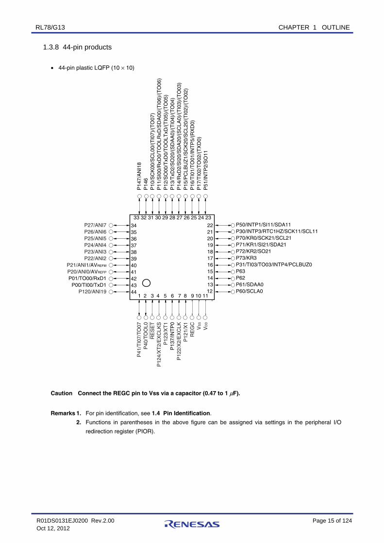
1.3.8 44-pin products
• 44-pin plastic LQFP (10 × 10)
33 32 31 30 29 28 27 26 25 24 23
1 2 3 4 5 6 7 8 9 10 11
3435363738394041424344
2221201918171615141312
P27/ANI7P26/ANI6P25/ANI5P24/ANI4P23/ANI3P22/ANI2
P21/ANI1/AVREFM
P20/ANI0/AVREFP
P01/TO00/RxD1P00/TI00/TxD1
P120/ANI19
P14
7/A
NI1
8P
146
P10
/SC
K00
/SC
L00/
(TI0
7)/(
TO
07)
P11
/SI0
0/R
xD0/
TO
OLR
xD/S
DA
00/(
TI0
6)/(
TO
06)
P12
/SO
00/T
xD0/
TO
OLT
xD/(
TI0
5)/(
TO
05)
P13
/TxD
2/S
O20
/(S
DA
A0)
/(T
I04)
/(T
O04
)P
14/R
xD2/
SI2
0/S
DA
20/(
SC
LA0)
/(T
I03)
/(T
O03
)P
15/P
CLB
UZ
1/S
CK
20/S
CL2
0/(T
I02)
/(T
O02
)P
16/T
I01/
TO
01/IN
TP
5/(R
XD
0)P
17/T
I02/
TO
02/(
TX
D0)
P51
/INT
P2/
SO
11
P41
/TI0
7/TO
07P
40/T
OO
L0R
ES
ET
P12
4/X
T2/
EX
CLK
SP
123/
XT
1P
137/
INT
P0
P12
2/X
2/E
XC
LKP
121/
X1
RE
GC
VS
S
VD
D
P50/INTP1/SI11/SDA11P30/INTP3/RTC1HZ/SCK11/SCL11P70/KR0/SCK21/SCL21P71/KR1/SI21/SDA21P72/KR2/SO21P73/KR3P31/TI03/TO03/INTP4/PCLBUZ0P63P62P61/SDAA0P60/SCLA0
Caution Connect the REGC pin to Vss via a capacitor (0.47 to 1 μF).
Remarks 1. For pin identification, see 1.4 Pin Identification.
2. Functions in parentheses in the above figure can be assigned via settings in the peripheral I/O
redirection register (PIOR).

RL78/G13 CHAPTER 1 OUTLINE
Page 16 of 124R01DS0131EJ0200 Rev.2.00 Oct 12, 2012
1.3.9 48-pin products
• 48-pin plastic LQFP (fine pitch) (7 × 7)
36 35 34 33 32 31 30 29 28 27 26 25
1 2 3 4 5 6 7 8 9 10 11 12
373839404142434445464748
242322212019181716151413
P120/ANI19P41/TI07/TO07
P40/TOOL0RESET
P124/XT2/EXCLKSP123/XT1
P137/INTP0P122/X2/EXCLK
P121/X1REGC
VSS
VDD
P14
0/P
CLB
UZ
0/IN
TP
6P
00/T
I00/
TxD
1P
01/T
O00
/RxD
1P
130
P20
/AN
I0/A
VR
EF
P
P21
/AN
I1/A
VR
EF
M
P22
/AN
I2P
23/A
NI3
P24
/AN
I4P
25/A
NI5
P26
/AN
I6P
27/A
NI7
P147/ANI18P146P10/SCK00/SCL00/(TI07)/(TO07)P11/SI00/RxD0/TOOLRxD/SDA00/(TI06)/(TO06)P12/SO00/TxD0/TOOLTxD/(TI05)/(TO05)P13/TxD2/SO20/(SDAA0)/(TI04)/(TO04)P14/RxD2/SI20/SDA20/(SCLA0)/(TI03)/(TO03)P15/PCLBUZ1/SCK20/SCL20/(TI02)/(TO02)P16/TI01/TO01/INTP5/(RXD0)P17/TI02/TO02/(TXD0)P51/INTP2/SO11P50/INTP1/SI11/SDA11
P60
/SC
LA0
P61
/SD
AA
0P
62P
63P
31/T
I03/
TO
03/IN
TP
4/(P
CLB
UZ
0)P
75/K
R5/
INT
P9/
SC
K01
/SC
L01
P74
/KR
4/IN
TP
8/S
I01/
SD
A01
P73
/KR
3/S
O01
P72
/KR
2/S
O21
P71
/KR
1/S
I21/
SD
A21
P70
/KR
0/S
CK
21/S
CL2
1P
30/IN
TP
3/R
TC
1HZ
/SC
K11
/SC
L11
Caution Connect the REGC pin to Vss via a capacitor (0.47 to 1 μF).
Remarks 1. For pin identification, see 1.4 Pin Identification.
2. Functions in parentheses in the above figure can be assigned via settings in the peripheral I/O
redirection register (PIOR).

RL78/G13 CHAPTER 1 OUTLINE
Page 17 of 124R01DS0131EJ0200 Rev.2.00 Oct 12, 2012
• 48-pin plastic WQFN (7 × 7)
242322212019181716151413
373839404142434445464748
36 35 34 33 32 31 30 29 28 27 26 25
1 2 3 4 5 6 7 8 9 10 11 12
P147/ANI18P146P10/SCK00/SCL00/(TI07)/(TO07)P11/SI00/RxD0/TOOLRxD/SDA00/(TI06)/(TO06)P12/SO00/TxD0/TOOLTxD/(TI05)/(TO05)P13/TxD2/SO20/(SDAA0)/(TI04)/(TO04)P14/RxD2/SI20/SDA20/(SCLA0)/(TI03)/(TO03)P15/PCLBUZ1/SCK20/SCL20/(TI02)/(TO02)P16/TI01/TO01/INTP5/(RXD0)P17/TI02/TO02/(TXD0)P51/INTP2/SO11P50/INTP1/SI11/SDA11
P120/ANI19P41/TI07/TO07
P40/TOOL0RESET
P124/XT2/EXCLKSP123/XT1
P137/INTP0P122/X2/EXCLK
P121/X1REGC
VSS
VDD
P14
0/P
CLB
UZ
0/IN
TP
6P
00/T
I00/
TxD
1P
01/T
O00
/RxD
1P
130
P20
/AN
I0/A
VR
EF
P
P21
/AN
I1/A
VR
EF
M
P22
/AN
I2P
23/A
NI3
P24
/AN
I4P
25/A
NI5
P26
/AN
I6P
27/A
NI7
P60
/SC
LA0
P61
/SD
AA
0P
62P
63P
31/T
I03/
TO
03/IN
TP
4/(P
CLB
UZ
0)P
75/K
R5/
INT
P9/
SC
K01
/SC
L01
P74
/KR
4/IN
TP
8/S
I01/
SD
A01
P73
/KR
3/S
O01
P72
/KR
2/S
O21
P71
/KR
1/S
I21/
SD
A21
P70
/KR
0/S
CK
21/S
CL2
1P
30/IN
TP
3/R
TC
1HZ
/SC
K11
/SC
L11
exposed die pad
Caution Connect the REGC pin to Vss via a capacitor (0.47 to 1 μF).
Remarks 1. For pin identification, see 1.4 Pin Identification.
2. Functions in parentheses in the above figure can be assigned via settings in the peripheral I/O
redirection register (PIOR).
RL78/G13 CHAPTER 1 OUTLINE
Page 18 of 124R01DS0131EJ0200 Rev.2.00 Oct 12, 2012
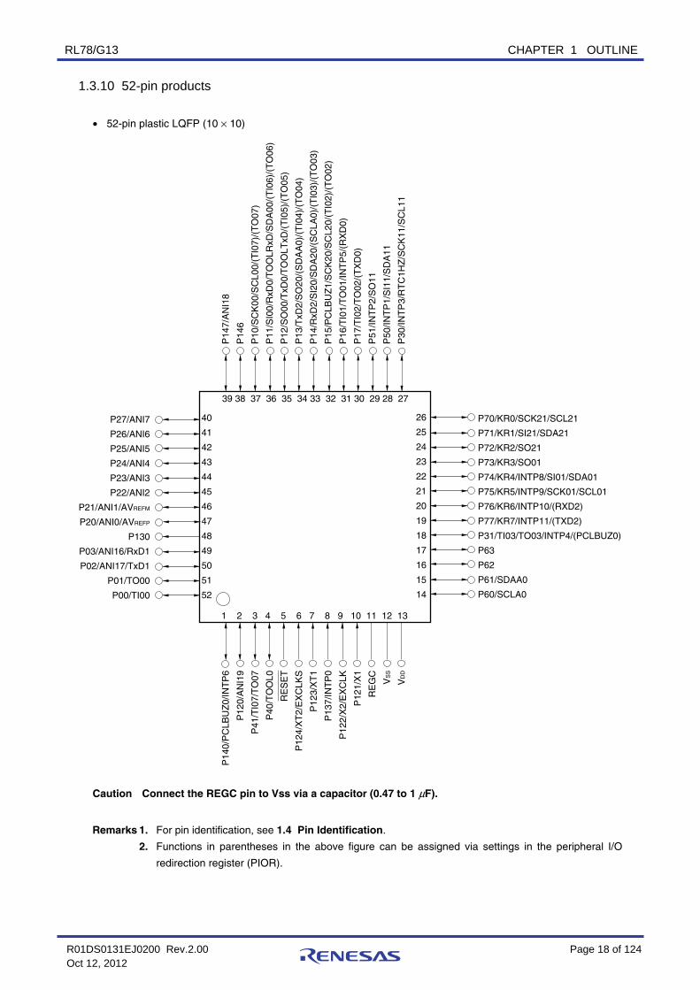
1.3.10 52-pin products
• 52-pin plastic LQFP (10 × 10)
1 2 3 4 5 6 7 8 9 10 11 12 13
39 38 37 36 35 34 33 32 31 30 29 28 27
P27/ANI7
P26/ANI6
P25/ANI5
P24/ANI4
P23/ANI3
P22/ANI2
P21/ANI1/AVREFM
P20/ANI0/AVREFP
P130
P03/ANI16/RxD1
P02/ANI17/TxD1
P01/TO00
P00/TI00
P14
0/P
CLB
UZ
0/IN
TP
6
P12
0/A
NI1
9
P41
/TI0
7/T
O07
P40
/TO
OL0
RE
SE
T
P12
4/X
T2/
EX
CLK
S
P12
3/X
T1
P13
7/IN
TP
0
P12
2/X
2/E
XC
LK
P12
1/X
1
RE
GC
VS
S
VD
D
P14
7/A
NI1
8
P14
6
P10
/SC
K00
/SC
L00/
(TI0
7)/(
TO
07)
P11
/SI0
0/R
xD0/
TO
OLR
xD/S
DA
00/(
TI0
6)/(
TO
06)
P12
/SO
00/T
xD0/
TO
OLT
xD/(
TI0
5)/(
TO
05)
P13
/TxD
2/S
O20
/(S
DA
A0)
/(T
I04)
/(T
O04
)
P14
/RxD
2/S
I20/
SD
A20
/(S
CLA
0)/(
TI0
3)/(
TO
03)
P15
/PC
LBU
Z1/
SC
K20
/SC
L20/
(TI0
2)/(
TO
02)
P16
/TI0
1/T
O01
/INT
P5/
(RX
D0)
P17
/TI0
2/T
O02
/(T
XD
0)
P51
/INT
P2/
SO
11
P50
/INT
P1/
SI1
1/S
DA
11
P30
/INT
P3/
RT
C1H
Z/S
CK
11/S
CL1
1
P70/KR0/SCK21/SCL21
P71/KR1/SI21/SDA21
P72/KR2/SO21
P73/KR3/SO01
P74/KR4/INTP8/SI01/SDA01
P75/KR5/INTP9/SCK01/SCL01
P76/KR6/INTP10/(RXD2)
P77/KR7/INTP11/(TXD2)
P31/TI03/TO03/INTP4/(PCLBUZ0)
P63
P62
P61/SDAA0
P60/SCLA0
26
25
24
23
22
21
20
19
18
17
16
15
14
40
41
42
43
44
45
46
47
48
49
50
51
52
Caution Connect the REGC pin to Vss via a capacitor (0.47 to 1 μF).
Remarks 1. For pin identification, see 1.4 Pin Identification.
2. Functions in parentheses in the above figure can be assigned via settings in the peripheral I/O
redirection register (PIOR).

RL78/G13 CHAPTER 1 OUTLINE
Page 19 of 124R01DS0131EJ0200 Rev.2.00 Oct 12, 2012
1.3.11 64-pin products
• 64-pin plastic LQFP (12 × 12)
• 64-pin plastic LQFP (fine pitch) (10 × 10)
1 2 3 4 5 6 7 8 9 10 11 12 13 14 15 16
48 47 46 45 44 43 42 41 40 39 38 37 36 35 34 33
P27/ANI7P26/ANI6P25/ANI5P24/ANI4P23/ANI3P22/ANI2
P21/ANI1/AVREFM
P20/ANI0/AVREFP
P130P04/SCK10/SCL10
P03/ANI16/SI10/RxD1/SDA10P02/ANI17/SO10/TxD1
P01/TO00P00/TI00
P141/PCLBUZ1/INTP7P140/PCLBUZ0/INTP6
P30/INTP3/RTC1HZ/SCK11/SCL11P05/TI05/TO05P06/TI06/TO06P70/KR0/SCK21/SCL21P71/KR1/SI21/SDA21P72/KR2/SO21P73/KR3/SO01P74/KR4/INTP8/SI01/SDA01P75/KR5/INTP9/SCK01/SCL01P76/KR6/INTP10/(RXD2)P77/KR7/INTP11/(TXD2)P31/TI03/TO03/INTP4/(PCLBUZ0)P63P62P61/SDAA0P60/SCLA0
P14
7/A
NI1
8P
146
P10
/SC
K00
/SC
L00/
(TI0
7)/(
TO
07)
P11
/SI0
0/R
xD0/
TO
OLR
xD/S
DA
00/(
TI0
6)/(
TO
06)
P12
/SO
00/T
xD0/
TO
OLT
xD/(
INT
P5)
/(T
I05)
/(T
O05
)P
13/T
xD2/
SO
20/(
SD
AA
0)/(
TI0
4)/(
TO
04)
P14
/RxD
2/S
I20/
SD
A20
/(S
CLA
0)/(
TI0
3)/(
TO
03)
P15
/SC
K20
/SC
L20/
(TI0
2)/(
TO
02)
P16
/TI0
1/T
O01
/INT
P5/
(SI0
0)/(
RX
D0)
P17
/TI0
2/T
O02
/(S
O00
)/(T
XD
0)P
55/(
PC
LBU
Z1)
/(S
CK
00)
P54
P53
/(IN
TP
11)
P52
/(IN
TP
10)
P51
/INT
P2/
SO
11P
50/IN
TP
1/S
I11/
SD
A11
P12
0/A
NI1
9P
43P
42/T
I04/
TO
04P
41/T
I07/
TO
07P
40/T
OO
L0R
ES
ET
P12
4/X
T2/
EX
CLK
SP
123/
XT
1P
137/
INT
P0
P12
2/X
2/E
XC
LKP
121/
X1
RE
GC
VS
S
EV
SS
0
VD
D
EV
DD
0
49505152535455565758596061626364
32313029282726252423222120191817
Cautions 1. Make EVSS0 pin the same potential as VSS pin.
2. Make VDD pin the potential that is higher than EVDD0 pin.
3. Connect the REGC pin to Vss via a capacitor (0.47 to 1 μF).
Remarks 1. For pin identification, see 1.4 Pin Identification.
2. When using the microcontroller for an application where the noise generated inside the
microcontroller must be reduced, it is recommended to supply separate powers to the VDD and
EVDD0 pins and connect the VSS and EVSS0 pins to separate ground lines.
3. Functions in parentheses in the above figure can be assigned via settings in the peripheral I/O
redirection register (PIOR).

RL78/G13 CHAPTER 1 OUTLINE
Page 20 of 124R01DS0131EJ0200 Rev.2.00 Oct 12, 2012
• 64-pin plastic FBGA (4 × 4)
1
H G F E D C B A
2
3
4
5
6
7
8
A B C D E F G H
Top View Bottom View
Index mark Pin No. Name Pin No. Name Pin No. Name Pin No. Name
A1 P05/TI05/TO05 C1 P51/INTP2/SO11 E1 P13/TxD2/SO20/ (SDAA0)/(TI04)/(TO04)
G1 P146
A2 P30/INTP3/RTC1HZ /SCK11/SCL11
C2 P71/KR1/SI21/SDA21 E2 P14/RxD2/SI20/SDA20/(SCLA0)/(TI03)/(TO03)
G2 P25/ANI5
A3 P70/KR0/SCK21 /SCL21
C3 P74/KR4/INTP8/SI01 /SDA01
E3 P15/SCK20/SCL20/ (TI02)/(TO02)
G3 P24/ANI4
A4 P75/KR5/INTP9 /SCK01/SCL01
C4 P52/(INTP10) E4 P16/TI01/TO01/INTP5/(SI00)/(RxD0)
G4 P22/ANI2
A5 P77/KR7/INTP11/ (TxD2)
C5 P53/(INTP11) E5 P03/ANI16/SI10/RxD1/SDA10
G5 P130
A6 P61/SDAA0 C6 P63 E6 P41/TI07/TO07 G6 P02/ANI17/SO10/TxD1
A7 P60/SCLA0 C7 VSS E7 RESET G7 P00/TI00
A8 EVDD0 C8 P121/X1 E8 P137/INTP0 G8 P124/XT2/EXCLKS
B1 P50/INTP1/SI11 /SDA11
D1 P55/(PCLBUZ1)/ (SCK00)
F1 P10/SCK00/SCL00/ (TI07)/(TO07)
H1 P147/ANI18
B2 P72/KR2/SO21 D2 P06/TI06/TO06 F2 P11/SI00/RxD0 /TOOLRxD/SDA00/ (TI06)/(TO06)
H2 P27/ANI7
B3 P73/KR3/SO01 D3 P17/TI02/TO02/ (SO00)/(TxD0)
F3 P12/SO00/TxD0 /TOOLTxD/(INTP5)/
(TI05)/(TO05)
H3 P26/ANI6
B4 P76/KR6/INTP10/ (RxD2)
D4 P54 F4 P21/ANI1/AVREFM H4 P23/ANI3
B5 P31/TI03/TO03 /INTP4/(PCLBUZ0)
D5 P42/TI04/TO04 F5 P04/SCK10/SCL10 H5 P20/ANI0/AVREFP
B6 P62 D6 P40/TOOL0 F6 P43 H6 P141/PCLBUZ1/INTP7
B7 VDD D7 REGC F7 P01/TO00 H7 P140/PCLBUZ0/INTP6
B8 EVSS0 D8 P122/X2/EXCLK F8 P123/XT1 H8 P120/ANI19
Cautions 1. Make EVSS0 pin the same potential as VSS pin.
2. Make VDD pin the potential that is higher than EVDD0 pin.
3. Connect the REGC pin to Vss via a capacitor (0.47 to 1 μF).
Remarks 1. For pin identification, see 1.4 Pin Identification.
2. When using the microcontroller for an application where the noise generated inside the
microcontroller must be reduced, it is recommended to supply separate powers to the VDD and
EVDD0 pins and connect the VSS and EVSS0 pins to separate ground lines.
3. Functions in parentheses in the above figure can be assigned via settings in the peripheral I/O
redirection register (PIOR).

RL78/G13 CHAPTER 1 OUTLINE
Page 21 of 124R01DS0131EJ0200 Rev.2.00 Oct 12, 2012
1.3.12 80-pin products
• 80-pin plastic LQFP (14 × 14)
• 80-pin plastic LQFP (fine pitch) (12 × 12)
P152/ANI10P151/ANI9P150/ANI8
P27/ANI7P26/ANI6P25/ANI5P24/ANI4P23/ANI3P22/ANI2
P21/ANI1/AVREFM
P20/ANI0/AVREFP
P130P04/SCK10/SCL10
P03/ANI16/SI10/RxD1/SDA10P02/ANI17/SO10/TxD1
P01/TO00P00/TI00
P144/SO30/TxD3P143/SI30/RxD3/SDA30
P142/SCK30/SCL30
P15
3/A
NI1
1P
100/
AN
I20
P14
7/A
NI1
8P
146
P11
1/(I
NT
P11
)P
110/
(IN
TP
10)
P10
/SC
K00
/SC
L00/
(TI0
7)/(
TO
07)
P11
/SI0
0/R
xD0/
TO
OLR
xD/S
DA
00/(
TI0
6)/(
TO
06)
P12
/SO
00/T
xD0/
TO
OLT
xD/(
INT
P5)
/(T
I05)
/(T
O05
)P
13/T
xD2/
SO
20/(
SD
AA
0)/(
TI0
4)/(
TO
04)
P14
/RxD
2/S
I20/
SD
A20
/(S
CLA
0)/(
TI0
3)/(
TO
03)
P15
/SC
K20
/SC
L20/
(TI0
2)/(
TO
02)
P16
/TI0
1/T
O01
/INT
P5/
(SI0
0)/(
RX
D0)
P17
/TI0
2/T
O02
/(S
O00
)/(T
XD
0)P
55/(
PC
LBU
Z1)
/(S
CK
00)
P54
/SC
K31
/SC
L31
P53
/SI3
1/S
DA
31P
52/S
O31
P51
/INT
P2/
SO
11P
50/IN
TP
1/S
I11/
SD
A11
1 2 3 4 5 6 7 8 9 10 11 12 13 14 15 16 17 18 19 20
60 59 58 57 56 55 54 53 52 51 50 49 48 47 46 45 44 43 42 41
P30/INTP3/RTC1HZ/SCK11/SCL11P05/TI05/TO05P06/TI06/TO06P70/KR0/SCK21/SCL21P71/KR1/SI21/SDA21P72/KR2/SO21P73/KR3P74/KR4/INTP8P75/KR5/INTP9P76/KR6/INTP10/(RXD2)P77/KR7/INTP11/(TXD2)P67/TI13/TO13P66/TI12/TO12P65/TI11/TO11P64/TI10/TO10P31/TI03/TO03/INTP4/(PCLBUZ0)P63/SDAA1P62/SCLA1P61/SDAA0P60/SCLA0
P14
1/P
CLB
UZ
1/IN
TP
7P
140/
PC
LBU
Z0/
INT
P6
P12
0/A
NI1
9P
45/S
O01
P44
/SI0
1/S
DA
01P
43/S
CK
01/S
CL0
1P
42/T
I04/
TO
04P
41/T
I07/
TO
07P
40/T
OO
L0R
ES
ET
P12
4/X
T2/
EX
CLK
SP
123/
XT
1P
137/
INT
P0
P12
2/X
2/E
XC
LKP
121/
X1
RE
GC
VS
S
EV
SS
0
VD
D
EV
DD
0
4039383736353433323130292827262524232221
6162636465666768697071727374757677787980
Cautions 1. Make EVSS0 pin the same potential as VSS pin.
2. Make VDD pin the potential that is higher than EVDD0 pin.
3. Connect the REGC pin to Vss via a capacitor (0.47 to 1 μF).
Remarks 1. For pin identification, see 1.4 Pin Identification.
2. When using the microcontroller for an application where the noise generated inside the
microcontroller must be reduced, it is recommended to supply separate powers to the VDD and
EVDD0 pins and connect the VSS and EVSS0 pins to separate ground lines.
3. Functions in parentheses in the above figure can be assigned via settings in the peripheral I/O
redirection register (PIOR).

RL78/G13 CHAPTER 1 OUTLINE
Page 22 of 124R01DS0131EJ0200 Rev.2.00 Oct 12, 2012
1.3.13 100-pin products
• 100-pin plastic LQFP (fine pitch) (14 × 14)
P14
2/S
CK
30/S
CL3
0P
141/
PC
LBU
Z1/
INT
P7
P14
0/P
CLB
UZ
0/IN
TP
6P
120/
AN
I19
P47
/INT
P2
P46
/INT
P1/
TI0
5/T
O05
P45
/SO
01P
44/S
I01/
SD
A01
P43
/SC
K01
/SC
L01
P42
/TI0
4/T
O04
P41
P40
/TO
OL0
RE
SE
TP
124/
XT
2/E
XC
LKS
P12
3/X
T1
P13
7/IN
TP
0P
122/
X2/
EX
CLK
P12
1/X
1R
EG
CV
SS
EV
SS
0
VD
D
EV
DD
0
P60
/SC
LA0
P61
/SD
AA
0
1 2 3 4 5 6 7 8 9 10 11 12 13 14 15 16 17 18 19 20 21 22 23 24 25
P10
0/A
NI2
0P
147/
AN
I18
P14
6/(I
NT
P4)
P11
1/(I
NT
P11
)P
110/
(IN
TP
10)
P10
1P
10/S
CK
00/S
CL0
0/(T
I07)
/(T
O07
)P
11/S
I00/
RxD
0/T
OO
LRxD
/SD
A00
/(T
I06)
/(T
O06
)P
12/S
O00
/TxD
0/T
OO
LTxD
/(IN
TP
5)/(
TI0
5)/(
TO
05)
P13
/TxD
2/S
O20
/(S
DA
A0)
/(T
I04)
/(T
O04
)P
14/R
xD2/
SI2
0/S
DA
20/(
SC
LA0)
/(T
I03)
/(T
O03
)P
15/S
CK
20/S
CL2
0/(T
I02)
/(T
O02
)P
16/T
I01/
TO
01/IN
TP
5/(S
I00)
/(R
XD
0)P
17/T
I02/
TO
02/(
SO
00)/
(TX
D0)
P57
/(IN
TP
3)P
56/(
INT
P1)
P55
/(P
CLB
UZ
1)/(
SC
K00
)P
54/S
CK
31/S
CL3
1P
53/S
I31/
SD
A31
P52
/SO
31P
51/S
O11
P50
/SI1
1/S
DA
11E
VD
D1
P30
/INT
P3/
RT
C1H
Z/S
CK
11/S
CL1
1P
87/(
INT
P9)
P156/ANI14P155/ANI13P154/ANI12P153/ANI11P152/ANI10P151/ANI9P150/ANI8P27/ANI7P26/ANI6P25/ANI5P24/ANI4P23/ANI3P22/ANI2
P21/ANI1/AVREFM
P20/ANI0/AVREFP
P130P102/TI06/TO06
P04/SCK10/SCL10P03/ANI16/SI10/RxD1/SDA10
P02/ANI17/SO10/TxD1P01/TO00P00/TI00
P145/TI07/TO07P144/SO30/TxD3
P143/SI30/RxD3/SDA30
P86/(INTP8)P85/(INTP7)P84/(INTP6)P83P82/(SO10)/(TXD1)P81/(SI10)/(RXD1)/(SDA10)P80/(SCK10)/(SCL10)EVSS1
P05P06P70/KR0/SCK21/SCL21P71/KR1/SI21/SDA21P72/KR2/SO21P73/KR3P74/KR4/INTP8P75/KR5/INTP9P76/KR6/INTP10/(RXD2)P77/KR7/INTP11/(TXD2)P67/TI13/TO13P66/TI12/TO12P65/TI11/TO11P64/TI10/TO10P31/TI03/TO03/INTP4/(PCLBUZ0)P63/SDAA1P62/SCLA1
75 74 73 72 71 70 69 68 67 66 65 64 63 62 61 60 59 58 57 56 55 54 53 52 5150494847464544434241403938373635343332313029282726
767778798081828384858687888990919293949596979899100
Cautions 1. Make EVSS0, EVSS1 pins the same potential as VSS pin.
2. Make VDD pin the potential that is higher than EVDD0, EVDD1 pins (EVDD0 = EVDD1).
3. Connect the REGC pin to Vss via a capacitor (0.47 to 1 μF).
Remarks 1. For pin identification, see 1.4 Pin Identification.
2. When using the microcontroller for an application where the noise generated inside the
microcontroller must be reduced, it is recommended to supply separate powers to the VDD, EVDD0
and EVDD1 pins and connect the VSS, EVSS0 and EVSS1 pins to separate ground lines.
3. Functions in parentheses in the above figure can be assigned via settings in the peripheral I/O
redirection register (PIOR).

RL78/G13 CHAPTER 1 OUTLINE
Page 23 of 124R01DS0131EJ0200 Rev.2.00 Oct 12, 2012
• 100-pin plastic LQFP (14 × 20)
P14
0/P
CLB
UZ
0/IN
TP
6P
141/
PC
LBU
Z1/
INT
P7
P14
2/S
CK
30/S
CL3
0P
143/
SI3
0/R
xD3/
SD
A30
P14
4/S
O30
/TxD
3P
145/
TI0
7/T
O07
P00
/TI0
0P
01/T
O00
P02
/AN
I17/
SO
10/T
xD1
P03
/AN
I16/
SI1
0/R
xD1/
SD
A10
P04
/SC
K10
/SC
L10
P10
2/T
I06/
TO
06P
130
P20
/AN
I0/A
VR
EF
P
P21
/AN
I1/A
VR
EF
M
P22
/AN
I2P
23/A
NI3
P24
/AN
I4P
25/A
NI5
P26
/AN
I6P
27/A
NI7
P15
0/A
NI8
P15
1/A
NI9
P15
2/A
NI1
0P
153/
AN
I11
P15
4/A
NI1
2P
155/
AN
I13
P15
6/A
NI1
4P
100/
AN
I20
P14
7/A
NI1
8
P60
/SC
LA0
P61
/SD
AA
0P
62/S
CLA
1P
63/S
DA
A1
P31
/TI0
3/T
O03
/INT
P4/
(PC
LBU
Z0)
P64
/TI1
0/T
O10
P65
/TI1
1/T
O11
P66
/TI1
2/T
O12
P67
/TI1
3/T
O13
P77
/KR
7/IN
TP
11/(
TX
D2)
P76
/KR
6/IN
TP
10/(
RX
D2)
P75
/KR
5/IN
TP
9P
74/K
R4/
INT
P8
P73
/KR
3P
72/K
R2/
SO
21P
71/K
R1/
SI2
1/S
DA
21P
70/K
R0/
SC
K21
/SC
L21
P06
P05
EV
SS
1
P80
/(S
CK
10)/
(SC
L10)
P81
/(S
I10)
/(R
XD
1)/(
SD
A10
)P
82/(
SO
10)/
(TX
D1)
P83
P84
/(IN
TP
6)P
85/(
INT
P7)
P86
/(IN
TP
8)P
87/(
INT
P9)
P30
/INT
P3/
RT
C1H
Z/S
CK
11/S
CL1
1E
VD
D1
80 79 78 77 76 75 74 73 72 71 70 69 68 67 66 65 64 63 62 61 60 59 58 57 56 55 54 53 52 51
1 2 3 4 5 6 7 8 9 10 11 12 13 14 15 16 17 18 19 20 21 22 23 24 25 26 27 28 29 30
50
49
48
47
46
45
44
43
42
41
40
39
38
37
36
35
34
33
32
31
81
82
83
84
85
86
87
88
89
90
91
92
93
94
95
96
97
98
99
100
P146/(INTP4)P111/(INTP11)P110/(INTP10)P101P10/SCK00/SCL00/(TI07)/(TO07)P11/SI00/RxD0/TOOLRxD/SDA00/(TI06)/(TO06)P12/SO00/TxD0/TOOLTxD/(INTP5)/(TI05)/(TO05)P13/TxD2/SO20/(SDAA0)/(TI04)/(TO04)P14/RxD2/SI20/SDA20/(SCLA0)/(TI03)/(TO03)P15/SCK20/SCL20/(TI02)/(TO02)P16/TI01/TO01/INTP5/(SI00)/(RXD0)P17/TI02/TO02/(SO00)/(TXD0)P57/(INTP3)P56/(INTP1)P55/(PCLBUZ1)/(SCK00)P54/SCK31/SCL31P53/SI31/SDA31 P52/SO31P51/SO11P50/SI11/SDA11
P120/ANI19 P47/INTP2
P46/INTP1/TI05/TO05P45/SO01
P44/SI01/SDA01P43/SCK01/SCL01
P42/TI04/TO04P41
P40/TOOL0RESET
P124/XT2/EXCLKSP123/XT1
P137/INTP0P122/X2/EXCLK
P121/X1REGC
VSS
EVSS0
VDD
EVDD0
Cautions 1. Make EVSS0, EVSS1 pins the same potential as VSS pin.
2. Make VDD pin the potential that is higher than EVDD0, EVDD1 pins (EVDD0 = EVDD1).
3. Connect the REGC pin to Vss via a capacitor (0.47 to 1 μF).
Remarks 1. For pin identification, see 1.4 Pin Identification.
2. When using the microcontroller for an application where the noise generated inside the
microcontroller must be reduced, it is recommended to supply separate powers to the VDD, EVDD0
and EVDD1 pins and connect the VSS, EVSS0 and EVSS1 pins to separate ground lines.
3. Functions in parentheses in the above figure can be assigned via settings in the peripheral I/O
redirection register (PIOR).

RL78/G13 CHAPTER 1 OUTLINE
Page 24 of 124R01DS0131EJ0200 Rev.2.00 Oct 12, 2012
1.3.14 128-pin products
• 128-pin plastic LQFP (fine pitch) (14 × 20)
P10
0/A
NI2
0P
147/
AN
I18
P14
6/(I
NT
P4)
P11
1/(I
NT
P11
)P
110/
(IN
TP
10)
P10
1P
117/
AN
I24
P11
6/A
NI2
5P
115/
AN
I26
P11
4P
113
P11
2P
97/S
O11
P96
/SI1
1/S
DA
11P
95/S
CK
11/S
CL1
1P
94P
93P
92P
91P
90P
10/S
CK
00/S
CL0
0/(T
I07)
/(T
O07
)P
11/S
I00/
RxD
0/T
OO
LRxD
/SD
A00
/(T
I06)
/(T
O06
)P
12/S
O00
/TxD
0/T
OO
LTxD
/(IN
TP
5)/(
TI0
5)/(
TO
05)
P13
/TxD
2/S
O20
/(S
DA
A0)
/(T
I04)
/(T
O04
)P
14/R
xD2/
SI2
0/S
DA
20/(
SC
LA0)
/(T
I03)
/(T
O03
)P
15/S
CK
20/S
CL2
0/(T
I02)
/(T
O02
)P
16/T
I01/
TO
01/IN
TP
5/(S
I00)
/(R
XD
0)P
17/T
I02/
TO
02/(
SO
00)/
(TX
D0)
P57
/(IN
TP
3)P
56/(
INT
P1)
P55
/(P
CLB
UZ
1)/(
SC
K00
)P
54/S
CK
31/S
CL3
1P
53/S
I31/
SD
A31
P52
/SO
31P
51P
50P
30/IN
TP
3/R
TC
1HZ
P87
/(IN
TP
9)
P14
2/S
CK
30/S
CL3
0P
141/
PC
LBU
Z1/
INT
P7
P14
0/P
CLB
UZ
0/IN
TP
6P
120/
AN
I19
P37
/AN
I21
P36
/AN
I22
P35
/AN
I23
P34
P33
P32
P10
6/T
I17/
TO
17P
105/
TI1
6/T
O16
P10
4/T
I15/
TO
15P
103/
TI1
4/T
O14
P47
/INT
P2
P46
/INT
P1/
TI0
5/T
O05
P45
/SO
01P
44/S
I01/
SD
A01
P43
/SC
K01
/SC
L01
P42
/TI0
4/T
O04
P41
P40
/TO
OL0
P12
7P
126
P12
5R
ES
ET
P12
4/X
T2/
EX
CLK
SP
123/
XT
1P
137/
INT
P0
P12
2/X
2/E
XC
LKP
121/
X1
RE
GC
VS
S
EV
SS
0
VD
D
EV
DD
0
P60
/SC
LA0
P61
/SD
AA
01 2 3 4 5 6 7 8 9 10 11 12 13 14 15 16 17 18 19 20 21 22 23 24 25 26 27 28 29 30 31 32 33 34 35 36 37 38
102 101 100 99 98 97 96 95 94 93 92 91 90 89 88 87 86 85 84 83 82 81 80 79 78 77 76 75 74 73 72 71 70 69 68 67 66 65103
104
105
106
107
108
109
110
111
112
113
114
115
116
117
118
119
120
121
122
123
124
125
126
127
128
64
63
62
61
60
59
58
57
56
55
54
53
52
51
50
49
48
47
46
45
44
43
42
41
40
39
P86/(INTP8)P85/(INTP7)P84/(INTP6)P83 P82/(SO10)/(TXD1)P81/(SI10)/(RXD1)/(SDA10)P80/(SCK10)/(SCL10)EVDD1 EVSS1 P05P06 P70/KR0/SCK21/SCL21 P71/KR1/SI21/SDA21 P72/KR2/SO21P73/KR3P74/KR4/INTP8 P75/KR5/INTP9P76/KR6/INTP10/(RXD2)P77/KR7/INTP11/(TXD2)P67/TI13/TO13 P66/TI12/TO12P65/TI11/TO11 P64/TI10/TO10P31/TI03/TO03/INTP4/(PCLBUZ0)P63/SDAA1P62/SCLA1
P156/ANI14P155/ANI13P154/ANI12P153/ANI11P152/ANI10P151/ANI9P150/ANI8P27/ANI7P26/ANI6P25/ANI5P24/ANI4P23/ANI3P22/ANI2
P21/ANI1/AVREFM
P20/ANI0/AVREFP
P130P102/TI06/TO06
P07P04/SCK10/SCL10
P03/ANI16/SI10/RxD1/SDA10P02/ANI17/SO10/TxD1
P01/TO00P00/TI00
P145/TI07/TO07P144/SO30/TxD3
P143/SI30/RxD3/SDA30
Cautions 1. Make EVSS0, EVSS1 pins the same potential as VSS pin.
2. Make VDD pin the potential that is higher than EVDD0, EVDD1 pins (EVDD0 = EVDD1).
3. Connect the REGC pin to Vss via a capacitor (0.47 to 1 μF).
Remarks 1. For pin identification, see 1.4 Pin Identification.
2. When using the microcontroller for an application where the noise generated inside the
microcontroller must be reduced, it is recommended to supply separate powers to the VDD, EVDD0
and EVDD1 pins and connect the VSS, EVSS0 and EVSS1 pins to separate ground lines.
3. Functions in parentheses in the above figure can be assigned via settings in the peripheral I/O
redirection register (PIOR).

RL78/G13 CHAPTER 1 OUTLINE
Page 25 of 124R01DS0131EJ0200 Rev.2.00 Oct 12, 2012
1.4 Pin Identification
ANI0 to ANI14,
ANI16 to ANI26: Analog input
AVREFM: A/D converter reference
potential (− side) input
AVREFP: A/D converter reference
potential (+ side) input
EVDD0, EVDD1: Power supply for port
EVSS0, EVSS1: Ground for port
EXCLK: External clock input (Main
system clock)
EXCLKS: External clock input
(Subsystem clock)
INTP0 to INTP11: Interrupt request from
peripheral
KR0 to KR7: Key return
P00 to P07: Port 0
P10 to P17: Port 1
P20 to P27: Port 2
P30 to P37: Port 3
P40 to P47: Port 4
P50 to P57: Port 5
P60 to P67: Port 6
P70 to P77: Port 7
P80 to P87: Port 8
P90 to P97: Port 9
P100 to P106: Port 10
P110 to P117: Port 11
P120 to P127: Port 12
P130, P137: Port 13
P140 to P147: Port 14
P150 to P156: Port 15
PCLBUZ0, PCLBUZ1: Programmable clock
output/buzzer output
REGC: Regulator capacitance
RESET: Reset
RTC1HZ: Real-time clock correction clock
(1 Hz) output
RxD0 to RxD3: Receive data
SCK00, SCK01, SCK10,
SCK11, SCK20, SCK21,
SCK30, SCK31: Serial clock input/output
SCLA0, SCLA1, SCL00,
SCL01, SCL10, SCL11,
SCL20,SCL21, SCL30,
SCL31: Serial clock output
SDAA0, SDAA1, SDA00,
SDA01,SDA10, SDA11,
SDA20,SDA21, SDA30,
SDA31: Serial data input/output
SI00, SI01, SI10, SI11,
SI20, SI21, SI30, SI31: Serial data input
SO00, SO01, SO10,
SO11, SO20, SO21,
SO30, SO31: Serial data output
TI00 to TI07,
TI10 to TI17: Timer input
TO00 to TO07,
TO10 to TO17: Timer output
TOOL0: Data input/output for tool
TOOLRxD, TOOLTxD: Data input/output for external device
TxD0 to TxD3: Transmit data
VDD: Power supply
VSS: Ground
X1, X2: Crystal oscillator (main system clock)
XT1, XT2: Crystal oscillator (subsystem clock)
<R>

RL78/G13 CHAPTER 1 OUTLINE
Page 26 of 124R01DS0131EJ0200 Rev.2.00 Oct 12, 2012
1.5 Block Diagram
1.5.1 20-pin products
PORT 1 P10 to P12, P16, P17
PORT 2 P20 to P223
PORT 3 P30
PORT 4
5
PORT 12 P121, P122
P40
VOLTAGEREGULATOR
REGC
INTERRUPTCONTROL
RAM
LOW-SPEEDON-CHIP
OSCILLATOR POWER ON RESET/VOLTAGE DETECTOR
POR/LVDCONTROL
RESET CONTROL
SYSTEMCONTROL RESET
X1/P121
X2/EXCLK/P122
HIGH-SPEEDON-CHIP
OSCILLATOR
ON-CHIP DEBUG TOOL0/P40
SERIAL ARRAY UNIT0 (4ch)
UART0
UART1
IIC00
RxD0/P11TxD0/P12
RxD1/P01TxD1/P00
SCL00/P10SDA00/P11
TIMER ARRAY UNIT (8ch)
ch2TI02/TO02/P17
ch3
ch0
ch1
ch4
ch5
ch6
ch7
INTP0/P137
INTP3/P30
A/D CONVERTER
3ANI0/P20 to ANI2/P22
AVREFP/P20AVREFM/P21
2
PORT 13 P137
CSI11SCK11/P30
SO11/P16SI11/P17
IIC11SCL11/P30SDA11/P17
TI00/P00TO00/P01
BCD ADJUSTMENT
12-BIT INTERVALTIMER
SCK00/P10
SO00/P12SI00/P11 CSI00
VSS TOOLRxD/P11, TOOLTxD/P12
VDD
INTP5/P16
PORT 0 P00, P012
WINDOWWATCHDOG
TIMER
REAL-TIMECLOCK
3ANI16/P01, ANI17/P00, ANI18/P147
DIRECT MEMORYACCESS CONTROL
PORT 14 P147
TI01/TO01/P16
MULTIPLIER&DIVIDER,
MULITIPLY-ACCUMULATOR
RL78CPU
CORE
CODE FLASH MEMORY
DATA FLASH MEMORY
CRC

RL78/G13 CHAPTER 1 OUTLINE
Page 27 of 124R01DS0131EJ0200 Rev.2.00 Oct 12, 2012
1.5.2 24-pin products
PORT 1 P10 to P12, P16, P17
PORT 2 P20 to P223
PORT 3 P30, P312
PORT 4
PORT 5
5
PORT 12 P121, P122
P40
P50
VOLTAGEREGULATOR
REGC
INTERRUPTCONTROL
RAM
WINDOWWATCHDOG
TIMER
POWER ON RESET/VOLTAGE DETECTOR
POR/LVDCONTROL
RESET CONTROL
SYSTEMCONTROL RESET
X1/P121
X2/EXCLK/P122
HIGH-SPEEDON-CHIP
OSCILLATOR
ON-CHIP DEBUG TOOL0/P40
SERIAL ARRAY UNIT0 (4ch)
UART0
UART1
IIC00
RxD0/P11TxD0/P12
RxD1/P01TxD1/P00
SCL00/P10SDA00/P11
TIMER ARRAY UNIT (8ch)
ch2TI02/TO02/P17
ch3TI03/TO03/P31
ch0
ch1
ch4
ch5
ch6
ch7
INTP0/P137
INTP3/P30,INTP4/P31
INTP1/P50
A/D CONVERTER
3ANI0/P20 to ANI2/P22
AVREFP/P20AVREFM/P21
2
PORT 13 P137
CSI11SCK11/P30
SO11/P17SI11/P50
IIC11SCL11/P30SDA11/P50
TI00/P00TO00/P01
BCD ADJUSTMENT
SCK00/P10
SO00/P12SI00/P11 CSI00
VSS TOOLRxD/P11, TOOLTxD/P12
VDD
SERIALINTERFACE IICA0
SDAA0/P61SCLA0/P60
2
INTP5/P16
MULTIPLIER&DIVIDER,
MULITIPLY-ACCUMULATOR
PORT 0 P00, P012
3ANI16/P01, ANI17/P00, ANI18/P147
DIRECT MEMORYACCESS CONTROL
PORT 6 P60, P612
PORT 14 P147
TI01/TO01/P16
BUZZER OUTPUT
PCLBUZ0/P31CLOCK OUTPUTCONTROL
REAL-TIMECLOCK
RL78CPU
CORE
CODE FLASH MEMORY
DATA FLASH MEMORY
CRC
LOW-SPEEDON-CHIP
OSCILLATOR
12-BIT INTERVALTIMER

RL78/G13 CHAPTER 1 OUTLINE
Page 28 of 124R01DS0131EJ0200 Rev.2.00 Oct 12, 2012
1.5.3 25-pin products
PORT 1 P10 to P12, P16, P17
PORT 2 P20 to P223
PORT 3 P30, P312
PORT 4
PORT 5
5
PORT 12 P121, P122
P40
P50
VOLTAGEREGULATOR
REGC
INTERRUPTCONTROL
RAM
POWER ON RESET/VOLTAGE DETECTOR
POR/LVDCONTROL
RESET CONTROL
SYSTEMCONTROL RESET
X1/P121
X2/EXCLK/P122
HIGH-SPEEDON-CHIP
OSCILLATOR
ON-CHIP DEBUG TOOL0/P40
SERIAL ARRAY UNIT0 (4ch)
UART0
UART1
IIC00
RxD0/P11TxD0/P12
RxD1/P01TxD1/P00
SCL00/P10SDA00/P11
TIMER ARRAY UNIT (8ch)
ch2TI02/TO02/P17
ch3TI03/TO03/P31
ch0
ch1
ch4
ch5
ch6
ch7
INTP0/P137
INTP3/P30,INTP4/P31
INTP1/P50
A/D CONVERTER
3ANI0/P20 to ANI2/P22
AVREFP/P20AVREFM/P21
2
PORT 13P137P130
CSI11SCK11/P30
SO11/P17SI11/P50
IIC11SCL11/P30SDA11/P50
TI00/P00TO00/P01
BCD ADJUSTMENT
SCK00/P10
SO00/P12SI00/P11 CSI00
VSS TOOLRxD/P11, TOOLTxD/P12
VDD
SERIALINTERFACE IICA0
SDAA0/P61SCLA0/P60
2
INTP5/P16
MULTIPLIER&DIVIDER,
MULITIPLY-ACCUMULATOR
PORT 0 P00, P012
3ANI16/P01, ANI17/P00, ANI18/P147
DIRECT MEMORYACCESS CONTROL
PORT 6 P60, P612
PORT 14 P147
TI01/TO01/P16
BUZZER OUTPUT
PCLBUZ0/P31CLOCK OUTPUTCONTROL
WINDOWWATCHDOG
TIMER
REAL-TIMECLOCK
RL78CPU
CORE
CODE FLASH MEMORY
DATA FLASH MEMORY
LOW-SPEEDON-CHIP
OSCILLATOR
12-BIT INTERVALTIMER
CRC

RL78/G13 CHAPTER 1 OUTLINE
Page 29 of 124R01DS0131EJ0200 Rev.2.00 Oct 12, 2012
1.5.4 30-pin products
PORT 1 P10 to P17
PORT 2 P20 to P234
PORT 3 P30, P312
PORT 4
PORT 5
8
PORT 12P121, P122
P40
P50, P512
VOLTAGEREGULATOR
REGC
INTERRUPTCONTROL
RAM
POWER ON RESET/VOLTAGE DETECTOR
POR/LVDCONTROL
RESET CONTROL
SYSTEMCONTROL RESET
X1/P121
X2/EXCLK/P122
HIGH-SPEEDON-CHIP
OSCILLATOR
ON-CHIP DEBUG TOOL0/P40
SERIAL ARRAY UNIT0 (4ch)
UART0
UART1
IIC00
RxD0/P11(RxD0/P16)
TxD0/P12(TxD0/P17)
RxD1/P01TxD1/P00
SCL00/P10SDA00/P11
TIMER ARRAY UNIT (8ch)
ch2TI02/TO02/P17
(TI02/TO02/P15)
ch3TI03/TO03/P31(TI03/TO03/P14)
ch0
ch1
ch4
ch5
ch6
ch7
2
INTP0/P137
INTP3/P30,INTP4/P31
INTP1/P50,INTP2/P51
RxD2/P14
A/D CONVERTER
4ANI0/P20 to ANI3/P23
AVREFP/P20AVREFM/P21
2
P120
PORT 13 P137
CSI11SCK11/P30
SO11/P51SI11/P50
IIC11SCL11/P30SDA11/P50
TI00/P00TO00/P01
BCD ADJUSTMENT
SCK00/P10
SO00/P12SI00/P11 CSI00
VSS TOOLRxD/P11, TOOLTxD/P12
VDD
SERIALINTERFACE IICA0
SDAA0/P61(SDAA0/P13)
SCLA0/P60(SCLA0/P14)
2
INTP5/P16
MULTIPLIER&DIVIDER,
MULITIPLY-ACCUMULATOR
PORT 0 P00, P012
BUZZER OUTPUT
CLOCK OUTPUTCONTROL
4ANI16/P01, ANI17/P00, ANI18/P147, ANI19/P120
SERIAL ARRAY UNIT1 (2ch)
UART2
LINSEL
IIC20
RxD2/P14TxD2/P13
SCL20/P15SDA20/P14
SCK20/P15
SO20/P13SI20/P14 CSI20 DIRECT MEMORY
ACCESS CONTROL
PORT 6 P60, P612
PORT 14 P147
TI01/TO01/P16
RxD2/P14
PCLBUZ0/P31, PCLBUZ1/P152
WINDOWWATCHDOG
TIMER
REAL-TIMECLOCK
RL78CPU
CORE
CODE FLASH MEMORY
DATA FLASH MEMORY
(TI04/TO04/P13)
(TI05/TO05/P12)
(TI06/TO06/P11)
(TI07/TO07/P10)
CRC
LOW-SPEEDON-CHIP
OSCILLATOR
12-BIT INTERVALTIMER
Remark Functions in parentheses in the above figure can be assigned via settings in the peripheral I/O
redirection register (PIOR).

RL78/G13 CHAPTER 1 OUTLINE
Page 30 of 124R01DS0131EJ0200 Rev.2.00 Oct 12, 2012
1.5.5 32-pin products
PORT 1 P10 to P17
PORT 2 P20 to P234
PORT 3 P30, P312
PORT 4
PORT 5
8
PORT 12P121, P122
P40
P50, P512
VOLTAGEREGULATOR
REGC
INTERRUPTCONTROL
RAMPOWER ON RESET/
VOLTAGE DETECTOR
POR/LVDCONTROL
RESET CONTROL
SYSTEMCONTROL RESET
X1/P121
X2/EXCLK/P122
HIGH-SPEEDON-CHIP
OSCILLATOR
ON-CHIP DEBUG TOOL0/P40
SERIAL ARRAY UNIT0 (4ch)
UART0
UART1
IIC00
RxD0/P11(RxD0/P16)TxD0/P12(TxD0/P17)
RxD1/P01TxD1/P00
SCL00/P10SDA00/P11
TIMER ARRAY UNIT (8ch)
ch2TI02/TO02/P17(TI02/TO02/P15)
ch3TI03/TO03/P31(TI03/TO03/P14)
ch0
ch1
ch4
ch5
ch6
ch7
2
INTP0/P137
INTP3/P30,INTP4/P31
INTP1/P50,INTP2/P51
RxD2/P14
A/D CONVERTER
4ANI0/P20 to ANI3/P23
AVREFP/P20AVREFM/P21
2
P120
PORT 13 P137
CSI11SCK11/P30
SO11/P51SI11/P50
IIC11SCL11/P30SDA11/P50
TI00/P00TO00/P01
BCD ADJUSTMENT
SCK00/P10
SO00/P12SI00/P11 CSI00
VSS TOOLRxD/P11, TOOLTxD/P12
VDD
SERIALINTERFACE IICA0
SDAA0/P61(SDAA0/P13)
SCLA0/P60(SCLA0/P14)
2
INTP5/P16
MULTIPLIER&DIVIDER,
MULITIPLY-ACCUMULATOR
PORT 0 P00, P012
BUZZER OUTPUT
CLOCK OUTPUTCONTROL
4ANI16/P01, ANI17/P00, ANI18/P147, ANI19/P120
SERIAL ARRAY UNIT1 (2ch)
UART2
LINSEL
IIC20
RxD2/P14TxD2/P13
SCL20/P15SDA20/P14
SCK20/P15
SO20/P13SI20/P14 CSI20
DIRECT MEMORYACCESS CONTROL
PORT 6
PORT 7 P70
P60 to P623
PORT 14 P147
TI01/TO01/P16
RxD2/P14
PCLBUZ0/P31, PCLBUZ1/P152
WINDOWWATCHDOG
TIMER
REAL-TIMECLOCK
RL78CPU
CORE
CODE FLASH MEMORY
DATA FLASH MEMORY
(TI04/TO04/P13)
(TI05/TO05/P12)
(TI06/TO06/P11)
(TI07/TO07/P10)
LOW-SPEEDON-CHIP
OSCILLATOR
12-BIT INTERVALTIMER
CRC
Remark Functions in parentheses in the above figure can be assigned via settings in the peripheral I/O
redirection register (PIOR).

RL78/G13 CHAPTER 1 OUTLINE
Page 31 of 124R01DS0131EJ0200 Rev.2.00 Oct 12, 2012
1.5.6 36-pin products
PORT 1 P10 to P17
PORT 2 P20 to P256
PORT 3 P30, P312
PORT 4
PORT 5
8
PORT 12P121, P122
P40
P50, P512
VOLTAGEREGULATOR
REGC
INTERRUPTCONTROL
RAM
POWER ON RESET/VOLTAGE DETECTOR
POR/LVDCONTROL
RESET CONTROL
SYSTEMCONTROL
RESETX1/P121X2/EXCLK/P122
HIGH-SPEEDON-CHIP
OSCILLATOR
ON-CHIP DEBUG TOOL0/P40
SERIAL ARRAY UNIT0 (4ch)
UART0
UART1
IIC00
RxD0/P11(RxD0/P16)
TxD0/P12(TxD0/P17)
RxD1/P01TxD1/P00
SCL00/P10SDA00/P11
TIMER ARRAY UNIT (8ch)
ch2TI02/TO02/P17
(TI02/TO02/P15)
ch3TI03/TO03/P31
(TI03/TO03/P14)
ch0
ch1
ch4
ch5
ch6
ch7
2
INTP0/P137
INTP3/P30,INTP4/P31
INTP1/P50,INTP2/P51
RxD2/P14
A/D CONVERTER
6ANI0/P20 to ANI5/P25
AVREFP/P20AVREFM/P21
2
P120
PORT 13 P137
CSI11SCK11/P30
SO11/P51SI11/P50
IIC11SCL11/P30SDA11/P50
TI00/P00TO00/P01
BCD ADJUSTMENT
SCK00/P10
SO00/P12SI00/P11 CSI00
VSS TOOLRxD/P11, TOOLTxD/P12
VDD
SERIALINTERFACE IICA0
SDAA0/P61(SDAA0/P13)
SCLA0/P60(SCLA0/P14)
2
INTP5/P16
MULTIPLIER&DIVIDER,
MULITIPLY-ACCUMULATOR
PORT 0 P00, P012
BUZZER OUTPUT
CLOCK OUTPUTCONTROL
REAL-TIMECLOCK
WINDOWWATCHDOG
TIMER
2 ANI18/P147, ANI19/P120
SERIAL ARRAY UNIT1 (2ch)
UART2
LINSEL
IIC20
RxD2/P14TxD2/P13
SCL20/P15SDA20/P14
IIC21SCL21/P70SDA21/P71
SCK20/P15
SO20/P13SI20/P14 CSI20
SCK21/P70
SO21/P72SI21/P71 CSI21
DIRECT MEMORYACCESS CONTROL
PORT 6
PORT 7 P70 to P723
P60 to P623
PORT 14 P147
TI01/TO01/P16
RxD2/P14
PCLBUZ0/P31, PCLBUZ1/P15
2
RL78CPU
CORE
CODE FLASH MEMORY
DATA FLASH MEMORY
(TI04/TO04/P13)
(TI05/TO05/P12)
(TI06/TO06/P11)
(TI07/TO07/P10)
LOW-SPEEDON-CHIP
OSCILLATOR
12-BIT INTERVALTIMER
CRC
Remark Functions in parentheses in the above figure can be assigned via settings in the peripheral I/O
redirection register (PIOR).

RL78/G13 CHAPTER 1 OUTLINE
Page 32 of 124R01DS0131EJ0200 Rev.2.00 Oct 12, 2012
1.5.7 40-pin products
PORT 1 P10 to P17
PORT 2 P20 to P267
PORT 3 P30, P312
PORT 4
PORT 5
8
PORT 12P121 to P124
P40
P50, P512
VOLTAGEREGULATOR
REGC
INTERRUPTCONTROL
RAM
WINDOWWATCHDOG
TIMER
POWER ON RESET/VOLTAGE DETECTOR
POR/LVDCONTROL
RESET CONTROL
SYSTEMCONTROL
RESETX1/P121X2/EXCLK/P122HIGH-SPEED
ON-CHIPOSCILLATOR
ON-CHIP DEBUG TOOL0/P40
REAL-TIMECLOCK
SERIAL ARRAY UNIT0 (4ch)
UART0
UART1
IIC00
RxD0/P11(RxD0/P16)TxD0/P12(TxD0/P17)
RxD1/P01TxD1/P00
SCL00/P10SDA00/P11
TIMER ARRAY UNIT (8ch)
ch2TI02/TO02/P17(TI02/TO02/P15)
ch3TI03/TO03/P31(TI03/TO03/P14)
ch0
ch1
ch4
ch5
ch6
ch7
2
INTP0/P137
INTP3/P30,INTP4/P31
INTP1/P50,INTP2/P51
RxD2/P14
A/D CONVERTER
7ANI0/P20 to ANI6/P26
AVREFP/P20AVREFM/P21
4
P120
PORT 13 P137
CSI11SCK11/P30
SO11/P51SI11/P50
IIC11SCL11/P30SDA11/P50
TI00/P00TO00/P01
BCD ADJUSTMENT
SCK00/P10
SO00/P12SI00/P11 CSI00
VSS TOOLRxD/P11, TOOLTxD/P12
VDD
SERIALINTERFACE IICA0
SDAA0/P61(SDAA0/P13)
SCLA0/P60(SCLA0/P14)
2
INTP5/P16
MULTIPLIER&DIVIDER,
MULITIPLY-ACCUMULATOR
XT1/P123
XT2/EXCLKS/P124
PORT 0 P00, P012
BUZZER OUTPUT
CLOCK OUTPUTCONTROL
KEY RETURN 4 KR0/P70 to KR3/P73
2 ANI18/P147, ANI19/P120
SERIAL ARRAY UNIT1 (2ch)
UART2
LINSEL
IIC20
RxD2/P14TxD2/P13
SCL20/P15SDA20/P14
IIC21SCL21/P70SDA21/P71
SCK20/P15
SO20/P13SI20/P14 CSI20
SCK21/P70
SO21/P72SI21/P71 CSI21
DIRECT MEMORYACCESS CONTROL
PORT 6
PORT 7 P70 to P734
P60 to P623
PORT 14 P147
TI01/TO01/P16
RTC1HZ/P30
PCLBUZ0/P31, PCLBUZ1/P15
2
RL78CPU
CORE
CODE FLASH MEMORY
DATA FLASH MEMORY
(TI04/TO04/P13)
(TI05/TO05/P12)
(TI06/TO06/P11)
RxD2/P14(TI07/TO07/P10)
LOW-SPEEDON-CHIP
OSCILLATOR
12-BIT INTERVALTIMER
CRC
Remark Functions in parentheses in the above figure can be assigned via settings in the peripheral I/O
redirection register (PIOR).

RL78/G13 CHAPTER 1 OUTLINE
Page 33 of 124R01DS0131EJ0200 Rev.2.00 Oct 12, 2012
1.5.8 44-pin products
PORT 1 P10 to P17
PORT 2 P20 to P278
PORT 3 P30, P312
PORT 4
PORT 5
8
PORT 12P121 to P124
P40, P412
P50, P512
VOLTAGEREGULATOR
REGC
INTERRUPTCONTROL
RAM
WINDOWWATCHDOG
TIMER
POWER ON RESET/VOLTAGE DETECTOR
POR/LVDCONTROL
RESET CONTROL
SYSTEMCONTROL
RESETX1/P121X2/EXCLK/P122HIGH-SPEED
ON-CHIPOSCILLATOR
ON-CHIP DEBUG TOOL0/P40
REAL-TIMECLOCK
SERIAL ARRAY UNIT0 (4ch)
UART0
UART1
IIC00
RxD0/P11(RxD0/P16)
TxD0/P12(TxD0/P17)
RxD1/P01TxD1/P00
SCL00/P10SDA00/P11
TIMER ARRAY UNIT (8ch)
ch2TI02/TO02/P17(TI02/TO02/P15)
ch3TI03/TO03/P31(TI03/TO03/P14)
ch0
ch1
ch4
ch5
ch6
ch7
2
INTP0/P137
INTP3/P30,INTP4/P31
INTP1/P50,INTP2/P51
RxD2/P14
A/D CONVERTER
8ANI0/P20 to ANI7/P27
AVREFP/P20AVREFM/P21
4
P120
PORT 13 P137
CSI11SCK11/P30
SO11/P51SI11/P50
IIC11SCL11/P30SDA11/P50
TI07/TO07/P41(TI07/TO07/P10)
TI00/P00TO00/P01
BCD ADJUSTMENT
SCK00/P10
SO00/P12SI00/P11 CSI00
VSS TOOLRxD/P11, TOOLTxD/P12
VDD
SERIALINTERFACE IICA0
SDAA0/P61(SDAA0/P13)
SCLA0/P60(SCLA0/P14)
2
INTP5/P16
MULTIPLIER&DIVIDER,
MULITIPLY-ACCUMULATOR
XT1/P123
XT2/EXCLKS/P124
PORT 0 P00, P012
BUZZER OUTPUT
CLOCK OUTPUTCONTROL
KEY RETURN 4 KR0/P70 to KR3/P73
2 ANI18/P147, ANI19/P120
SERIAL ARRAY UNIT1 (2ch)
UART2
LINSEL
IIC20
RxD2/P14TxD2/P13
SCL20/P15SDA20/P14
IIC21SCL21/P70SDA21/P71
SCK20/P15
SO20/P13SI20/P14 CSI20
SCK21/P70
SO21/P72SI21/P71 CSI21
DIRECT MEMORYACCESS CONTROL
PORT 6
PORT 7 P70 to P734
P60 to P634
PORT 14 P146, P1472
TI01/TO01/P16
RTC1HZ/P30
RxD2/P14
PCLBUZ0/P31, PCLBUZ1/P15
2
RL78CPU
CORE
CODE FLASH MEMORY
DATA FLASH MEMORY
(TI04/TO04/P13)
(TI05/TO05/P12)
(TI06/TO06/P11)
LOW-SPEEDON-CHIP
OSCILLATOR
12-BIT INTERVALTIMER
CRC
Remark Functions in parentheses in the above figure can be assigned via settings in the peripheral I/O
redirection register (PIOR).

RL78/G13 CHAPTER 1 OUTLINE
Page 34 of 124R01DS0131EJ0200 Rev.2.00 Oct 12, 2012
1.5.9 48-pin products
PORT 1 P10 to P17
PORT 2 P20 to P278
PORT 3 P30, P312
PORT 4
PORT 5
8
PORT 12P121 to P124
P40, P412
P50, P512
VOLTAGEREGULATOR
REGC
INTERRUPTCONTROL
RAM
WINDOWWATCHDOG
TIMER
POWER ON RESET/VOLTAGE DETECTOR
POR/LVDCONTROL
RESET CONTROL
SYSTEMCONTROL
RESETX1/P121X2/EXCLK/P122HIGH-SPEED
ON-CHIPOSCILLATOR
ON-CHIP DEBUG TOOL0/P40
SERIAL ARRAY UNIT0 (4ch)
UART0
UART1
IIC00
RxD0/P11(RxD0/P16)TxD0/P12(TxD0/P17)
RxD1/P01TxD1/P00
SCL00/P10SDA00/P11
TIMER ARRAY UNIT (8ch)
ch2TI02/TO02/P17(TI02/TO02/P15)
ch3TI03/TO03/P31(TI03/TO03/P14)
ch0
ch1
ch4
ch5
ch6
ch7
INTP8/P74, INTP9/P75
2
INTP0/P137
INTP3/P30,INTP4/P31
INTP6/P140
INTP1/P50,INTP2/P51
RxD2/P14
A/D CONVERTER
8ANI0/P20 to ANI7/P27
AVREFP/P20AVREFM/P21
4
P120
PORT 13P130P137
CSI11SCK11/P30
SO11/P51SI11/P50
IIC01SCL01/P75SDA01/P74
IIC11SCL11/P30SDA11/P50
TI07/TO07/P41(TI07/TO07/P10)
TI00/P00TO00/P01
BCD ADJUSTMENT
SCK00/P10
SO00/P12SI00/P11 CSI00
VSS TOOLRxD/P11, TOOLTxD/P12
VDD
SERIALINTERFACE IICA0
SDAA0/P61(SDAA0/P13)
SCLA0/P60(SCLA0/P14)
2
2
INTP5/P16
MULTIPLIER&DIVIDER,
MULITIPLY-ACCUMULATOR
XT1/P123
XT2/EXCLKS/P124
PORT 0 P00, P012
BUZZER OUTPUT PCLBUZ0/P140(PCLBUZ0/P31), PCLBUZ1/P15CLOCK OUTPUT
CONTROL
KEY RETURN 6 KR0/P70 to KR5/P75
2 ANI18/P147, ANI19/P120
SCK01/P75
SO01/P73SI01/P74 CSI01
SERIAL ARRAY UNIT1 (2ch)
UART2
LINSEL
IIC20
RxD2/P14TxD2/P13
SCL20/P15SDA20/P14
IIC21SCL21/P70SDA21/P71
SCK20/P15
SO20/P13SI20/P14 CSI20
SCK21/P70
SO21/P72SI21/P71 CSI21
DIRECT MEMORYACCESS CONTROL
PORT 6
PORT 7 P70 to P756
P60 to P634
PORT 14P140, P146, P147
3
2
TI01/TO01/P16
RTC1HZ/P30
RxD2/P14
REAL-TIMECLOCK RL78
CPUCORE
CODE FLASH MEMORY
DATA FLASH MEMORY
(TI04/TO04/P13)
(TI05/TO05/P12)
(TI06/TO06/P11)
LOW-SPEEDON-CHIP
OSCILLATOR
12-BIT INTERVALTIMER
CRC
Remark Functions in parentheses in the above figure can be assigned via settings in the peripheral I/O
redirection register (PIOR).

RL78/G13 CHAPTER 1 OUTLINE
Page 35 of 124R01DS0131EJ0200 Rev.2.00 Oct 12, 2012
1.5.10 52-pin products
PORT 1 P10 to P17
PORT 2 P20 to P278
PORT 3 P30, P312
PORT 4
PORT 5
8
PORT 12P121 to P124
P40, P412
P50, P512
VOLTAGEREGULATOR
REGC
INTERRUPTCONTROL
RAM
POWER ON RESET/VOLTAGE DETECTOR
POR/LVDCONTROL
RESET CONTROL
SYSTEMCONTROL
RESETX1/P121X2/EXCLK/P122HIGH-SPEED
ON-CHIPOSCILLATOR
ON-CHIP DEBUG TOOL0/P40
SERIAL ARRAY UNIT0 (4ch)
UART0
UART1
IIC00
RxD0/P11(RxD0/P16)TxD0/P12(TxD0/P17)
RxD1/P03TxD1/P02
SCL00/P10SDA00/P11
TIMER ARRAY UNIT (8ch)
ch2TI02/TO02/P17
(TI02/TO02/P15)
ch3TI03/TO03/P31(TI03/TO03/P14)
ch0
ch1
ch4
ch5
ch6
ch7
INTP8/P74 to INTP11/P77
2
INTP0/P137
INTP3/P30,INTP4/P31
INTP6/P140
INTP1/P50,INTP2/P51
RxD2/P14 (RxD2/P76)
A/D CONVERTER
8ANI0/P20 to ANI7/P27
AVREFP/P20AVREFM/P21
4
P120
PORT 13P130P137
CSI11SCK11/P30
SO11/P51SI11/P50
IIC01SCL01/P75SDA01/P74
IIC11SCL11/P30SDA11/P50
TI07/TO07/P41(TI07/TO07/P10)
TI00/P00TO00/P01
BCD ADJUSTMENT
SCK00/P10
SO00/P12SI00/P11 CSI00
VSS TOOLRxD/P11, TOOLTxD/P12
VDD
SERIALINTERFACE IICA0
SDAA0/P61(SDAA0/P13)
SCLA0/P60(SCLA0/P14)
4
2
INTP5/P16
MULTIPLIER&DIVIDER,
MULITIPLY-ACCUMULATOR
XT1/P123
XT2/EXCLKS/P124
PORT 0 P00 to P034
BUZZER OUTPUT PCLBUZ0/P140(PCLBUZ0/P31), PCLBUZ1/P15CLOCK OUTPUT
CONTROL
KEY RETURN 8 KR0/P70 to KR7/P77
WINDOWWATCHDOG
TIMER
4ANI16/P03, ANI17/P02,ANI18/P147, ANI19/P120
SCK01/P75
SO01/P73SI01/P74 CSI01
SERIAL ARRAY UNIT1 (2ch)
UART2
LINSEL
IIC20
RxD2/P14(RxD2/P76)
TxD2/P13(TxD2/P77)
SCL20/P15SDA20/P14
IIC21SCL21/P70SDA21/P71
SCK20/P15
SO20/P13SI20/P14 CSI20
SCK21/P70
SO21/P72SI21/P71 CSI21
DIRECT MEMORYACCESS CONTROL
PORT 6
PORT 7 P70 to P778
P60 to P634
PORT 14P140, P146, P147
3
2
TI01/TO01/P16
RTC1HZ/P30
RxD2/P14(RxD2/P76)
REAL-TIMECLOCK
RL78CPU
CORE
CODE FLASH MEMORY
DATA FLASH MEMORY
(TI04/TO04/P13)
(TI05/TO05/P12)
(TI06/TO06/P11)
LOW-SPEEDON-CHIP
OSCILLATOR
12-BIT INTERVALTIMER
CRC
Remark Functions in parentheses in the above figure can be assigned via settings in the peripheral I/O
redirection register (PIOR).

RL78/G13 CHAPTER 1 OUTLINE
Page 36 of 124R01DS0131EJ0200 Rev.2.00 Oct 12, 2012
1.5.11 64-pin products
PORT 1 P10 to P17
PORT 2 P20 to P278
PORT 3 P30, P312
PORT 4
PORT 5
8
PORT 12P121 to P124
P40 to P434
P50 to P556
VOLTAGEREGULATOR
REGC
INTERRUPTCONTROL
RAM
RL78CPU
CORE
POWER ON RESET/VOLTAGE DETECTOR
POR/LVDCONTROL
RESET CONTROL
SYSTEMCONTROL
RESETX1/P121X2/EXCLK/P122HIGH-SPEED
ON-CHIPOSCILLATOR
ON-CHIP DEBUG TOOL0/P40
SERIAL ARRAY UNIT0 (4ch)
UART0
UART1
IIC00
RxD0/P11(RxD0/P16)TxD0/P12(TxD0/P17)
RxD1/P03TxD1/P02
SCL00/P10SDA00/P11
TIMER ARRAY UNIT (8ch)
ch2TI02/TO02/P17
(TI02/TO02/P15)
ch3TI03/TO03/P31(TI03/TO03/P14)
ch0
ch1
ch4TI04/TO04/P42
(TI04/TO04/P13)
ch5TI05/TO05/P05
(TI05/TO05/P12)
ch6TI06/TO06/P06
(TI06/TO06/P11)
ch7
INTP8/P74,INTP9/P75
2
INTP0/P137
INTP3/P30,INTP4/P31
INTP6/P140,INTP7/P141
INTP1/P50,INTP2/P51
RxD2/P14 (RxD2/P76)
CSI10SCK10/P04
SO10/P02SI10/P03
A/D CONVERTER
8ANI0/P20 to ANI7/P27
AVREFP/P20AVREFM/P21
4
P120
PORT 13P130P137
CSI11SCK11/P30
SO11/P51SI11/P50
IIC01SCL01/P75SDA01/P74
IIC10SCL10/P04SDA10/P03
IIC11SCL11/P30SDA11/P50
TI07/TO07/P41(TI07/TO07/P10)
TI00/P00TO00/P01
BCD ADJUSTMENT
SCK00/P10(SCK00/P55)
SO00/P12(SO00/P17)SI00/P11(SI00/P16) CSI00
VSS,EVSS0
TOOLRxD/P11, TOOLTxD/P12
VDD,EVDD0
SERIALINTERFACE IICA0
SDAA0/P61(SDAA0/P13)
SCLA0/P60(SCLA0/P14)
2
2
2
INTP5/P16(INTP5/P12)
MULTIPLIER&DIVIDER,
MULITIPLY-ACCUMULATOR
XT1/P123
XT2/EXCLKS/P124
PORT 0 P00 to P067
BUZZER OUTPUT PCLBUZ0/P140(PCLBUZ0/P31), PCLBUZ1/P141(PCLBUZ1/P55)CLOCK OUTPUT
CONTROL
KEY RETURN 8 KR0/P70 to KR7/P77
WINDOWWATCHDOG
TIMER
4ANI16/P03, ANI17/P02,ANI18/P147, ANI19/P120
SCK01/P75
SO01/P73SI01/P74 CSI01
SERIAL ARRAY UNIT1 (2ch)
UART2
LINSEL
IIC20
RxD2/P14(RxD2/P76)
TxD2/P13(TxD2/P77)
SCL20/P15SDA20/P14
IIC21SCL21/P70SDA21/P71
SCK20/P15
SO20/P13SI20/P14 CSI20
SCK21/P70
SO21/P72SI21/P71 CSI21
DIRECT MEMORYACCESS CONTROL
PORT 6
PORT 7 P70 to P778
P60 to P634
PORT 14P140, P141, P146, P147
4
2
TI01/TO01/P16
RTC1HZ/P30
RxD2/P14(RxD2/P76)
REAL-TIMECLOCK
CODE FLASH MEMORY
DATA FLASH MEMORY
INTP10/P76(INTP10/P52),INTP11/P77(INTP11/P53)
2
LOW-SPEEDON-CHIP
OSCILLATOR
CRC
12-BIT INTERVALTIMER
Remark Functions in parentheses in the above figure can be assigned via settings in the peripheral I/O
redirection register (PIOR).

RL78/G13 CHAPTER 1 OUTLINE
Page 37 of 124R01DS0131EJ0200 Rev.2.00 Oct 12, 2012
1.5.12 80-pin products
PORT 1
PORT 2 P20 to P278
PORT 3 P30, P312
PORT 4
PORT 5
P10 to P178
P40 to P456
P50 to P556
VOLTAGEREGULATOR
REGC
INTERRUPTCONTROL
RAM
WINDOWWATCHDOG
TIMER
POWER ON RESET/VOLTAGE DETECTOR
POR/LVDCONTROL
RESET CONTROL
SYSTEMCONTROL
RESETX1/P121X2/EXCLK/P122HIGH-SPEED
ON-CHIPOSCILLATOR
ON-CHIP DEBUG TOOL0/P40
SERIAL ARRAY UNIT0 (4ch)
UART0
UART1
IIC00
RxD0/P11(RxD0/P16)TxD0/P12(TxD0/P17)
RxD1/P03TxD1/P02
SCL00/P10SDA00/P11
TIMER ARRAY UNIT0 (8ch)
ch2TI02/TO02/P17
(TI02/TO02/P15)
ch3TI03/TO03/P31(TI03/TO03/P14)
ch0
ch1
ch4TI04/TO04/P42
(TI04/TO04/P13)
ch5TI05/TO05/P05
(TI05/TO05/P12)
ch6TI06/TO06/P06
(TI06/TO06/P11)
ch7
INTP8/P74,INTP9/P75
2
INTP0/P137
INTP3/P30,INTP4/P31
INTP6/P140,INTP7/P141
INTP1/P50,INTP2/P51
RxD2/P14 (RxD2/P76)
CSI10SCK10/P04
SO10/P02SI10/P03
A/D CONVERTER
8 ANI0/P20 to ANI7/P27
AVREFP/P20AVREFM/P21
CSI11SCK11/P30
SO11/P51SI11/P50
IIC01SCL01/P43SDA01/P44
IIC10SCL10/P04SDA10/P03
IIC11SCL11/P30SDA11/P50
TI07/TO07/P41(TI07/TO07/P10)
TI00/P00TO00/P01
BCD ADJUSTMENT
SO00/P12(SO00/P17)SI00/P11(SI00/P16) CSI00
VSS,EVSS0
TOOLRxD/P11, TOOLTxD/P12
VDD,EVDD0
SERIALINTERFACE IICA0 SCLA0/P60(SCLA0/P14)
SDAA0/P61(SDAA0/P13)
2
2
2
INTP5/P16(INTP5/P12)
MULTIPLIER&DIVIDER,
MULITIPLY-ACCUMULATOR
XT1/P123
XT2/EXCLKS/P124
PORT 0 P00 to P067
BUZZER OUTPUT PCLBUZ0/P140(PCLBUZ0/P31), PCLBUZ1/P141(PCLBUZ1/P55)
CLOCK OUTPUTCONTROL
KEY RETURN 8 KR0/P70 to KR7/P77
5ANI16/P03, ANI17/P02,ANI18/P147, ANI19/P120, ANI20/P100
SCK01/P43
SO01/P45SI01/P44 CSI01
DIRECT MEMORYACCESS CONTROL
PORT 6
PORT 7 P70 to P778
P60 to P678
PORT 10 P100
2
TI01/TO01/P16
RTC1HZ/P30
RxD2/P14(RxD2/P76)
4 ANI8/P150 to ANI11/P153
PORT 11 P110, P1112
PORT 12P121 to P1244
P120
PORT 13P130P137
PORT 14 P140 to P144,P146, P147
7
PORT 15 P150 to P1534
SERIAL ARRAY UNIT1 (4ch)
UART3
IIC20
RxD2/P14(RxD2/P76)TxD2/P13(TxD2/P77)
RxD3/P143TxD3/P144
SCL20/P15SDA20/P14
CSI30SCK30/P142
SO30/P144SI30/P143
CSI31SCK31/P54
SO31/P52SI31/P53
IIC21SCL21/P70SDA21/P71
IIC30SCL30/P142SDA30/P143
IIC31SCL31/P54SDA31/P53
SCK20/P15
SO20/P13SI20/P14 CSI20
SCK21/P70
SO21/P72SI21/P71 CSI21
UART2
LINSEL
TIMER ARRAY UNIT1 (4ch)
ch2
ch3
ch0
ch1
TI12/TO12/P66
TI13/TO13/P67
TI11/TO11/P65
TI10/TO10/P64
SERIALINTERFACE IICA1
SDAA1/P63SCLA1/P62
REAL-TIMECLOCK
RL78CPU
CORE
CODE FLASH MEMORY
DATA FLASH MEMORY
INTP10/P76(INTP10/P110),INTP11/P77(INTP11/P111)
SCK00/P10(SCK00/P55)
2
CRC
LOW-SPEEDON-CHIP
OSCILLATOR
12-BIT INTERVALTIMER
Remark Functions in parentheses in the above figure can be assigned via settings in the peripheral I/O
redirection register (PIOR).

RL78/G13 CHAPTER 1 OUTLINE
Page 38 of 124R01DS0131EJ0200 Rev.2.00 Oct 12, 2012
1.5.13 100-pin products
SCK10/P04(SCK10/P80)
PORT 1 P10 to P17
PORT 2 P20 to P278
PORT 3 P30, P312
PORT 4
PORT 5
8
PORT 8
P40 to P478
P50 to P578
VOLTAGEREGULATOR
REGC
INTERRUPTCONTROL
RAM
WINDOWWATCHDOG
TIMER
POWER ON RESET/VOLTAGE DETECTOR
POR/LVDCONTROL
RESET CONTROL
SYSTEMCONTROL
RESETX1/P121X2/EXCLK/P122HIGH-SPEED
ON-CHIPOSCILLATOR
ON-CHIP DEBUG TOOL0/P40
SERIAL ARRAY UNIT0 (4ch)
UART0
UART1
IIC00
RxD0/P11(RxD0/P16)TxD0/P12(TxD0/P17)
RxD1/P03(RxD1/P81)TxD1/P02(TxD1/P82)
SCL00/P10SDA00/P11
TIMER ARRAY UNIT0 (8ch)
ch2TI02/TO02/P17
(TI02/TO02/P15)
ch3TI03/TO03/P31
(TI03/TO03/P14)
ch0
ch1
ch4TI04/TO04/P42
(TI04/TO04/P13)
ch5TI05/TO05/P46(TI05/TO05/P12)
ch6TI06/TO06/P102(TI06/TO06/P11)
ch7
INTP8/P74(INTP8/P86), INTP9/P75(INTP9/P87)
2
INTP0/P137
INTP3/P30(INTP3/P57),INTP4/P31(INTP4/P146)
INTP6/P140(INTP6/P84),INTP7/P141(INTP7/P85)
INTP1/P46(INTP1/P56),INTP2/P47
RxD2/P14 (RxD2/P76)
CSI10
SO10/P02(SO10/P82)SI10/P03(SI10/P81)
A/D CONVERTER
8 ANI0/P20 to ANI7/P27
AVREFP/P20AVREFM/P21
CSI11SCK11/P30
SO11/P51SI11/P50
IIC01SCL01/P43SDA01/P44
IIC10SCL10/P04(SCL10/P80)SDA10/P03(SDA10/P81)
IIC11SCL11/P30SDA11/P50
TI07/TO07/P145(TI07/TO07/P10)
TI00/P00TO00/P01
BCD ADJUSTMENT
SCK00/P10(SCK00/P55)
SO00/P12(SO00/P17)SI00/P11(SI00/P16) CSI00
VSS,EVSS0,EVSS1
TOOLRxD/P11, TOOLTxD/P12
VDD,EVDD0,EVDD1
SERIALINTERFACE IICA0
SDAA0/P61(SDAA0/P13)SCLA0/P60(SCLA0/P14)
2
2
2
INTP5/P16(INTP5/P12)
MULTIPLIER&DIVIDER,
MULITIPLY-ACCUMULATOR
XT1/P123
XT2/EXCLKS/P124
PORT 0 P00 to P067
KEY RETURN 8 KR0/P70 to KR7/P77
5ANI16/P03, ANI17/P02,ANI18/P147, ANI19/P120, ANI20/P100
SCK01/P43
SO01/P45SI01/P44 CSI01
DIRECT MEMORYACCESS CONTROL
PORT 6
PORT 7 P70 to P778
P60 to P678
PORT 10 P100 to P1023
BUZZER OUTPUT PCLBUZ0/P140(PCLBUZ0/P31), PCLBUZ1/P141(PCLBUZ1/P55)
CLOCK OUTPUTCONTROL
2
TI01/TO01/P16
RTC1HZ/P30
RxD2/P14(RxD2/P76)
7 ANI8/P150 to ANI14/P156
PORT 11 P110, P1112
PORT 12P121 to P1244
P120
PORT 13P130P137
PORT 14 P140 to P1478
PORT 15 P150 to P1567
P80 to P878
SERIAL ARRAY UNIT1 (4ch)
UART3
IIC20
RxD2/P14(RxD2/P76)TxD2/P13(TxD2/P77)
RxD3/P143TxD3/P144
SCL20/P15SDA20/P14
CSI30SCK30/P142
SO30/P144SI30/P143
CSI31SCK31/P54
SO31/P52SI31/P53
IIC21SCL21/P70SDA21/P71
IIC30SCL30/P142SDA30/P143
IIC31SCL31/P54SDA31/P53
SCK20/P15
SO20/P13SI20/P14 CSI20
SCK21/P70
SO21/P72SI21/P71 CSI21
UART2
LINSEL
TIMER ARRAY UNIT1 (4ch)
ch2
ch3
ch0
ch1
TI12/TO12/P66
TI13/TO13/P67
TI11/TO11/P65
TI10/TO10/P64
SERIALINTERFACE IICA1
SDAA1/P63SCLA1/P62
REAL-TIMECLOCK
RL78CPU
CORE
CODE FLASH MEMORY
DATA FLASH MEMORY
INTP10/P76(INTP10/P110), INTP11/P77(INTP11/P111)
2
CRC
LOW-SPEEDON-CHIP
OSCILLATOR
12-BIT INTERVALTIMER
Remark Functions in parentheses in the above figure can be assigned via settings in the peripheral I/O
redirection register (PIOR).

RL78/G13 CHAPTER 1 OUTLINE
Page 39 of 124R01DS0131EJ0200 Rev.2.00 Oct 12, 2012
1.5.14 128-pin products
SCK10/P04(SCK10/P80)
SCK00/P10(SCK00/P55)
PORT 1 P10 to P17
PORT 2 P20 to P278
PORT 3 P30 to P378
PORT 4
PORT 5
8
PORT 8
P40 to P478
P50 to P578
VOLTAGEREGULATOR
REGC
INTERRUPTCONTROL
RAM
POWER ON RESET/VOLTAGE DETECTOR
POR/LVDCONTROL
RESET CONTROL
SYSTEMCONTROL
RESETX1/P121X2/EXCLK/P122HIGH-SPEED
ON-CHIPOSCILLATOR
ON-CHIP DEBUG TOOL0/P40
SERIAL ARRAY UNIT0 (4ch)
UART0
UART1
IIC00
RxD0/P11(RxD0/P16)TxD0/P12(TxD0/P17)
RxD1/P03(RxD1/P81)TxD1/P02(TxD1/P82)
SCL00/P10SDA00/P11
TIMER ARRAY UNIT0 (8ch)
ch2TI02/TO02/P17
(TI02/TO02/P15)
ch3TI03/TO03/P31
(TI03/TO03/P14)
ch0
ch1
ch4TI04/TO04/P42
(TI04/TO04/P13)
ch5TI05/TO05/P46(TI05/TO05/P12)
ch6TI06/TO06/P102(TI06/TO06/P11)
ch7
INTP8/P74 (INTP8/P86),INTP9/P75 (INTP9/P87)
2
INTP0/P137
INTP3/P30 (INTP3/P57),INTP4/P31 (INTP4/P146)
INTP6/P140 (INTP6/P84),INTP7/P141 (INTP7/P85)
INTP1/P46 (INTP1/P56),INTP2/P47
RxD2/P14 (RxD2/P76)
CSI10
SO10/P02(SO10/P82)SI10/P03(SI10/P81)
A/D CONVERTER
8 ANI0/P20 to ANI7/P27
AVREFP/P20AVREFM/P21
PORT 9
CSI11SCK11/P95
SO11/P97SI11/P96
IIC01SCL01/P43SDA01/P44
IIC10SCL10/P04(SCL10/P80)SDA10/P03(SDA10/P81)
IIC11SCL11/P95SDA11/P96
TI07/TO07/P145(TI07/TO07/P10)
TI00/P00TO00/P01
SO00/P12(SO00/P17)SI00/P11(SI00/P16) CSI00
VSS,EVSS0,EVSS1
TOOLRxD/P11, TOOLTxD/P12
VDD,EVDD0,EVDD1
2
2
2
INTP5/P16 (INTP5/P12)
XT1/P123
XT2/EXCLKS/P124
PORT 0 P00 to P078
KEY RETURN 8 KR0/P70 to KR7/P77
11ANI16/P03, ANI17/P02,ANI18/P147, ANI19/P120, ANI20/P100, ANI21/37, ANI22/P36, ANI23/P35, ANI24/P117, ANI25/P116, ANI26/P115 SCK01/P43
SO01/P45SI01/P44 CSI01
PORT 6
PORT 7 P70 to P778
P60 to P678
PORT 10 P100 to P1067
TI01/TO01/P16
RxD2/P14(RxD2/P76)
7 ANI8/P150 to ANI14/P156
PORT 11 P110 to P1178
PORT 12P121 to P1244
P120, P125 to P127
PORT 13P130P137
PORT 14 P140 to P1478
4
PORT 15 P150 to P1567
P90 to P978
P80 to P878
SERIAL ARRAY UNIT1 (4ch)
UART3
IIC20
RxD2/P14(RxD2/P76)TxD2/P13(TxD2/P77)
RxD3/P143TxD3/P144
SCL20/P15SDA20/P14
CSI30SCK30/P142
SO30/P144SI30/P143
CSI31SCK31/P54
SO31/P52SI31/P53
IIC21SCL21/P70SDA21/P71
IIC30SCL30/P142SDA30/P143
IIC31SCL31/P54SDA31/P53
SCK20/P15
SO20/P13SI20/P14 CSI20
SCK21/P70
SO21/P72SI21/P71 CSI21
UART2
LINSEL
TIMER ARRAY UNIT1 (8ch)
ch2
ch3
ch0
ch1
ch4
ch5
ch6
ch7
TI12/TO12/P66
TI13/TO13/P67
TI14/TO14/P103
TI15/TO15/P104
TI16/TO16/P105
TI17/TO17/P106
TI11/TO11/P65
TI10/TO10/P64
WINDOWWATCHDOG
TIMER
BCD ADJUSTMENT
SERIALINTERFACE IICA0
SDAA0/P61(SDAA0/P13)SCLA0/P60(SCLA0/P14)
MULTIPLIER&DIVIDER,
MULITIPLY-ACCUMULATOR
BUZZER OUTPUT PCLBUZ0/P140(PCLBUZ0/P31), PCLBUZ1/P141(PCLBUZ1/P55)
CLOCK OUTPUTCONTROL
DIRECT MEMORYACCESS CONTROL
2
RTC1HZ/P30
SERIALINTERFACE IICA1
SDAA1/P63SCLA1/P62
REAL-TIMECLOCK
RL78CPU
CORE
CODE FLASH MEMORY
DATA FLASH MEMORY
2INTP10/P76 (INTP10/P110),INTP11/P77 (INTP11/P111)
CRC
LOW-SPEEDON-CHIP
OSCILLATOR
12-BIT INTERVALTIMER
Remark Functions in parentheses in the above figure can be assigned via settings in the peripheral I/O
redirection register (PIOR).

RL78/G13 CHAPTER 1 OUTLINE
Page 40 of 124R01DS0131EJ0200 Rev.2.00 Oct 12, 2012
1.6 Outline of Functions
[20-pin, 24-pin, 25-pin, 30-pin, 32-pin, 36-pin products]
Caution This outline describes the functions at the time when Peripheral I/O redirection register (PIOR)
is set to 00H other than timer output.
(1/2)
20-pin 24-pin 25-pin 30-pin 32-pin 36-pin Item
R5F
1006x
R5F
1016x
R5F
1007x
R5F
1017x
R5F
1008x
R5F
1018x
R5F
100Ax
R5F
101Ax
R5F
100Bx
R5F
101Bx
R5F
100Cx
R5F
101Cx
Code flash memory (KB) 16 to 64 16 to 64 16 to 64 16 to 128 16 to 128 16 to 128
Data flash memory (KB) 4 − 4 − 4 − 4 to 8 − 4 to 8 − 4 to 8 −
RAM (KB) 2 to 4Note1 2 to 4Note1 2 to 4Note1 2 to 12Note1 2 to 12Note1 2 to 12Note1
Memory space 1 MB
High-speed system clock
X1 (crystal/ceramic) oscillation, external main system clock input (EXCLK) 1 to 20 MHz: VDD = 2.7 to 5.5 V, 1 to 8 MHz: VDD = 1.8 to 2.7 V, 1 to 4 MHz: VDD = 1.6 to 1.8 V
Main system clock
High-speed on-chip oscillator
HS (High-speed main) mode: 1 to 32 MHz (VDD = 2.7 to 5.5 V), HS (High-speed main) mode: 1 to 16 MHz (VDD = 2.4 to 5.5 V), LS (Low-speed main) mode: 1 to 8 MHz (VDD = 1.8 to 5.5 V), LV (Low-voltage main) mode: 1 to 4 MHz (VDD = 1.6 to 5.5 V)
Subsystem clock −
Low-speed on-chip oscillator 15 kHz (TYP.)
General-purpose register (8-bit register × 8) × 4 banks
0.03125 μs (High-speed on-chip oscillator: fIH = 32 MHz operation) Minimum instruction execution time 0.05 μs (High-speed system clock: fMX = 20 MHz operation)
Instruction set • Data transfer (8/16 bits) • Adder and subtractor/logical operation (8/16 bits) • Multiplication (8 bits × 8 bits) • Rotate, barrel shift, and bit manipulation (Set, reset, test, and Boolean operation), etc.
I/O port Total 16 20 21 26 28 32
CMOS I/O 13 15 15 21 22 26
CMOS input 3 3 3 3 3 3
CMOS output − − 1 − − −
N-ch O.D I/O (6 V tolerance)
− 2 2 2 3 3
16-bit timer 8 channels
Watchdog timer 1 channel
Timer
Real-time clock (RTC) 1 channel
12-bit interval timer (IT)
1 channel
Timer output 3 channels (PWM outputs: 2 Note 2)
4 channels (PWM outputs: 3 Note 2)
4 channels (PWM outputs: 3 Note 2),
8 channels Note 3 (PWM outputs: 7 Note 2)
RTC output −
Notes 1. In the case of the 4 KB, this is about 3 KB when the self-programming function and data flash function are used.
2. The number of outputs varies, depending on the setting of channels in use and the number of the master.
3. When setting to PIOR = 1
<R>
<R>

RL78/G13 CHAPTER 1 OUTLINE
Page 41 of 124R01DS0131EJ0200 Rev.2.00 Oct 12, 2012
(2/2)
20-pin 24-pin 25-pin 30-pin 32-pin 36-pin Item
R5F
1006x
R5F
1016x
R5F
1007x
R5F
1017x
R5F
1008x
R5F
1018x
R5F
100Ax
R5F
101Ax
R5F
100Bx
R5F
101Bx
R5F
100Cx
R5F
101Cx
− 1 1 2 2 2 Clock output/buzzer output
• 2.44 kHz, 4.88 kHz, 9.76 kHz, 1.25 MHz, 2.5 MHz, 5 MHz, 10 MHz
(Main system clock: fMAIN = 20 MHz operation)
8/10-bit resolution A/D converter 6 channels 6 channels 6 channels 8 channels 8 channels 8 channels
Serial interface [20-pin, 24-pin, 25-pin products]
• CSI: 1 channel/simplified I2C: 1 channel/UART: 1 channel
• CSI: 1 channel/simplified I2C: 1 channel/UART: 1 channel
[30-pin, 32-pin products]
• CSI: 1 channel/simplified I2C: 1 channel/UART: 1 channel
• CSI: 1 channel/simplified I2C: 1 channel/UART: 1 channel
• CSI: 1 channel/simplified I2C: 1 channel/UART (UART supporting LIN-bus): 1 channel
[36-pin products]
• CSI: 1 channel/simplified I2C: 1 channel/UART: 1 channel
• CSI: 1 channel/simplified I2C: 1 channel/UART: 1 channel
• CSI: 2 channel/simplified I2C: 2 channel/UART (UART supporting LIN-bus): 1 channel
I2C bus − 1 channel 1 channel 1 channel 1 channel 1 channel
Multiplier and divider/multiply-
accumulator
• 16 bits × 16 bits = 32 bits (Unsigned or signed)
• 32 bits ÷ 32 bits = 32 bits (Unsigned)
• 16 bits × 16 bits + 32 bits = 32 bits (Unsigned or signed)
DMA controller 2 channels
Internal 23 24 24 27 27 27 Vectored interrupt
sources External 3 5 5 6 6 6
Key interrupt −
Reset • Reset by RESET pin
• Internal reset by watchdog timer
• Internal reset by power-on-reset
• Internal reset by voltage detector
• Internal reset by illegal instruction execution Note
• Internal reset by RAM parity error
• Internal reset by illegal-memory access
Power-on-reset circuit • Power-on-reset: 1.51 ±0.03 V
• Power-down-reset: 1.50 ±0.03 V
Voltage detector • Rising edge : 1.67 V to 4.06 V (14 stages)
• Falling edge : 1.63 V to 3.98 V (14 stages)
On-chip debug function Provided
Power supply voltage VDD = 1.6 to 5.5 V
Operating ambient temperature TA = −40 to +85 °C
Note The illegal instruction is generated when instruction code FFH is executed.
Reset by the illegal instruction execution not issued by emulation with the in-circuit emulator or on-chip
debug emulator.
<R>

RL78/G13 CHAPTER 1 OUTLINE
Page 42 of 124R01DS0131EJ0200 Rev.2.00 Oct 12, 2012
[40-pin, 44-pin, 48-pin, 52-pin, 64-pin products] Caution This outline describes the functions at the time when Peripheral I/O redirection register (PIOR)
is set to 00H other than timer output.
(1/2)
40-pin 44-pin 48-pin 52-pin 64-pin Item
R5F
100Ex
R5F
101Ex
R5F
100Fx
R5F
101Fx
R5F
100Gx
R5F
101Gx
R5F
100Jx
R5F
101Jx
R5F
100Lx
R5F
101Lx
Code flash memory (KB) 16 to 192 16 to 512 16 to 512 32 to 512 32 to 512
Data flash memory (KB) 4 to 8 − 4 to 8 − 4 to 8 − 4 to 8 − 4 to 8 −
RAM (KB) 2 to 16Note1 2 to 32Note1 2 to 32Note1 2 to 32Note1 2 to 32Note1
Memory space 1 MB
High-speed system clock
X1 (crystal/ceramic) oscillation, external main system clock input (EXCLK) 1 to 20 MHz: VDD = 2.7 to 5.5 V, 1 to 8 MHz: VDD = 1.8 to 2.7 V, 1 to 4 MHz: VDD = 1.6 to 1.8 V
Main system clock
High-speed on-chip oscillator
HS (High-speed main) mode: 1 to 32 MHz (VDD = 2.7 to 5.5 V), HS (High-speed main) mode: 1 to 16 MHz (VDD = 2.4 to 5.5 V), LS (Low-speed main) mode: 1 to 8 MHz (VDD = 1.8 to 5.5 V), LV (Low-voltage main) mode: 1 to 4 MHz (VDD = 1.6 to 5.5 V)
Subsystem clock XT1 (crystal) oscillation, external subsystem clock input (EXCLKS) 32.768 kHz
Low-speed on-chip oscillator 15 kHz (TYP.)
General-purpose register (8-bit register × 8) × 4 banks
0.03125 μs (High-speed on-chip oscillator: fIH = 32 MHz operation)
0.05 μs (High-speed system clock: fMX = 20 MHz operation)
Minimum instruction execution time
30.5 μs (Subsystem clock: fSUB = 32.768 kHz operation)
Instruction set • Data transfer (8/16 bits) • Adder and subtractor/logical operation (8/16 bits) • Multiplication (8 bits × 8 bits) • Rotate, barrel shift, and bit manipulation (Set, reset, test, and Boolean operation), etc.
I/O port Total 36 40 44 48 58
CMOS I/O 28 31 34 38 48
CMOS input 5 5 5 5 5
CMOS output − − 1 1 1
N-ch O.D I/O (6 V tolerance)
3 4 4 4 4
16-bit timer 8 channels
Watchdog timer 1 channel
Timer
Real-time clock (RTC) 1 channel
12-bit interval timer (IT) 1 channel
Timer output 4 channels (PWM outputs: 3 Note 2), 8 channels Note 3 (PWM outputs: 7 Note 2)
5 channels (PWM outputs: 4 Note 2), 8 channels Note 3 (PWM outputs: 7 Note 2)
8 channels (PWM outputs: 7 Note 2)
RTC output 1 • 1 Hz (subsystem clock: fSUB = 32.768 kHz)
Notes 1. In the case of the 4 KB, this is about 3 KB when the self-programming function and data flash function are used.
In the case of the 20 KB, this is about 19 KB when the self-programming function and data flash function are used.
In the case of the 32 KB, this is about 31 KB when the self-programming function and data flash function are used.
2. The number of outputs varies, depending on the setting of channels in use and the number of the master. 3. When setting to PIOR = 1
<R>
<R>
<R>

RL78/G13 CHAPTER 1 OUTLINE
Page 43 of 124R01DS0131EJ0200 Rev.2.00 Oct 12, 2012
(2/2)
40-pin 44-pin 48-pin 52-pin 64-pin Item
R5F
100Ex
R5F
101Ex
R5F
100Fx
R5F
101Fx
R5F
100Gx
R5F
101Gx
R5F
100Jx
R5F
101Jx
R5F
100Lx
R5F
101Lx
2 2 2 2 2 Clock output/buzzer output
• 2.44 kHz, 4.88 kHz, 9.76 kHz, 1.25 MHz, 2.5 MHz, 5 MHz, 10 MHz
(Main system clock: fMAIN = 20 MHz operation)
• 256 Hz, 512 Hz, 1.024 kHz, 2.048 kHz, 4.096 kHz, 8.192 kHz, 16.384 kHz, 32.768 kHz
(Subsystem clock: fSUB = 32.768 kHz operation)
8/10-bit resolution A/D converter 9 channels 10 channels 10 channels 12 channels 12 channels
Serial interface [40-pin, 44-pin products]
• CSI: 1 channel/simplified I2C: 1 channel/UART: 1 channel
• CSI: 1 channel/simplified I2C: 1 channel/UART: 1 channel
• CSI: 2 channels/simplified I2C: 2 channels/UART (UART supporting LIN-bus): 1 channel
[48-pin, 52-pin products]
• CSI: 2 channels/simplified I2C: 2 channels/UART: 1 channel
• CSI: 1 channel/simplified I2C: 1 channel/UART: 1 channel
• CSI: 2 channels/simplified I2C: 2 channels/UART (UART supporting LIN-bus): 1 channel
[64-pin products]
• CSI: 2 channels/simplified I2C: 2 channels/UART: 1 channel
• CSI: 2 channels/simplified I2C: 2 channels/UART: 1 channel
• CSI: 2 channels/simplified I2C: 2 channels/UART (UART supporting LIN-bus): 1 channel
I2C bus 1 channel 1 channel 1 channel 1 channel 1 channel
Multiplier and divider/multiply-
accumulator
• 16 bits × 16 bits = 32 bits (Unsigned or signed)
• 32 bits ÷ 32 bits = 32 bits (Unsigned)
• 16 bits × 16 bits + 32 bits = 32 bits (Unsigned or signed)
DMA controller 2 channels
Internal 27 27 27 27 27 Vectored
interrupt sources External 7 7 10 12 13
Key interrupt 4 4 6 8 8
Reset • Reset by RESET pin
• Internal reset by watchdog timer
• Internal reset by power-on-reset
• Internal reset by voltage detector
• Internal reset by illegal instruction execution Note
• Internal reset by RAM parity error
• Internal reset by illegal-memory access
Power-on-reset circuit • Power-on-reset: 1.51 ±0.03 V
• Power-down-reset: 1.50 ±0.03 V
Voltage detector • Rising edge : 1.67 V to 4.06 V (14 stages)
• Falling edge : 1.63 V to 3.98 V (14 stages)
On-chip debug function Provided
Power supply voltage VDD = 1.6 to 5.5 V
Operating ambient temperature TA = −40 to +85 °C
Note The illegal instruction is generated when instruction code FFH is executed.
Reset by the illegal instruction execution not issued by emulation with the in-circuit emulator or on-chip
debug emulator.
<R>

RL78/G13 CHAPTER 1 OUTLINE
Page 44 of 124R01DS0131EJ0200 Rev.2.00 Oct 12, 2012
[80-pin, 100-pin, 128-pin products]
Caution This outline describes the functions at the time when Peripheral I/O redirection register (PIOR)
is set to 00H.
(1/2)
80-pin 100-pin 128-pin Item
R5F100Mx R5F101Mx R5F100Px R5F101Px R5F100Sx R5F101Sx
Code flash memory (KB) 96 to 512 96 to 512 192 to 512
Data flash memory (KB) 8 − 8 − 8 −
RAM (KB) 8 to 32 Note 1 8 to 32 Note 1 16 to 32 Note 1
Memory space 1 MB
High-speed system clock
X1 (crystal/ceramic) oscillation, external main system clock input (EXCLK) 1 to 20 MHz: VDD = 2.7 to 5.5 V, 1 to 8 MHz: VDD = 1.8 to 2.7 V, 1 to 4 MHz: VDD = 1.6 to 1.8 V
Main system clock
High-speed on-chip oscillator
HS (High-speed main) mode: 1 to 32 MHz (VDD = 2.7 to 5.5 V), HS (High-speed main) mode: 1 to 16 MHz (VDD = 2.4 to 5.5 V), LS (Low-speed main) mode: 1 to 8 MHz (VDD = 1.8 to 5.5 V), LV (Low-voltage main) mode: 1 to 4 MHz (VDD = 1.6 to 5.5 V)
Subsystem clock XT1 (crystal) oscillation, external subsystem clock input (EXCLKS) 32.768 kHz
Low-speed on-chip oscillator 15 kHz (TYP.)
General-purpose register (8-bit register × 8) × 4 banks
0.03125 μs (High-speed on-chip oscillator: fIH = 32 MHz operation)
0.05 μs (High-speed system clock: fMX = 20 MHz operation)
Minimum instruction execution time
30.5 μs (Subsystem clock: fSUB = 32.768 kHz operation)
Instruction set • Data transfer (8/16 bits) • Adder and subtractor/logical operation (8/16 bits) • Multiplication (8 bits × 8 bits) • Rotate, barrel shift, and bit manipulation (Set, reset, test, and Boolean operation), etc.
I/O port Total 74 92 120
CMOS I/O 64 82 110
CMOS input 5 5 5
CMOS output 1 1 1
N-ch O.D I/O (6 V tolerance)
4 4 4
16-bit timer 12 channels 12 channels 16 channels
Watchdog timer 1 channel 1 channel 1 channel
Timer
Real-time clock (RTC) 1 channel 1 channel 1 channel
12-bit interval timer (IT) 1 channel 1 channel 1 channel
Timer output 12 channels (PWM outputs: 10 Note 2)
12 channels (PWM outputs: 10 Note 2)
16 channels (PWM outputs: 14 Note 2)
RTC output 1 • 1 Hz (subsystem clock: fSUB = 32.768 kHz)
Notes 1. In the case of the 20 KB, this is about 19 KB when the self-programming function and data flash
function are used.
In the case of the 32 KB, this is about 31 KB when the self-programming function and data flash
function are used.
2. The number of outputs varies, depending on the setting of channels in use and the number of the
master
<R>
<R>
<R>

RL78/G13 CHAPTER 1 OUTLINE
Page 45 of 124R01DS0131EJ0200 Rev.2.00 Oct 12, 2012
(2/2)
80-pin 100-pin 128-pin Item
R5F100Mx R5F101Mx R5F100Px R5F101Px R5F100Sx R5F101Sx
2 2 2 Clock output/buzzer output
• 2.44 kHz, 4.88 kHz, 9.76 kHz, 1.25 MHz, 2.5 MHz, 5 MHz, 10 MHz
(Main system clock: fMAIN = 20 MHz operation)
• 256 Hz, 512 Hz, 1.024 kHz, 2.048 kHz, 4.096 kHz, 8.192 kHz, 16.384 kHz, 32.768 kHz
(Subsystem clock: fSUB = 32.768 kHz operation)
8/10-bit resolution A/D converter 17 channels 20 channels 26 channels
Serial interface [80-pin, 100-pin, 128-pin products]
• CSI: 2 channels/simplified I2C: 2 channels/UART: 1 channel
• CSI: 2 channels/simplified I2C: 2 channels/UART: 1 channel
• CSI: 2 channels/simplified I2C: 2 channels/UART (UART supporting LIN-bus): 1
channel
• CSI: 2 channels/simplified I2C: 2 channels/UART: 1 channel
I2C bus 2 channel 2 channel 2 channel
Multiplier and divider/multiply-
accumulator
• 16 bits × 16 bits = 32 bits (Unsigned or signed)
• 32 bits ÷ 32 bits = 32 bits (Unsigned)
• 16 bits × 16 bits + 32 bits = 32 bits (Unsigned or signed)
DMA controller 4 channels
Internal 37 37 41 Vectored
interrupt sources External 13 13 13
Key interrupt 8 8 8
Reset • Reset by RESET pin
• Internal reset by watchdog timer
• Internal reset by power-on-reset
• Internal reset by voltage detector
• Internal reset by illegal instruction execution Note
• Internal reset by RAM parity error
• Internal reset by illegal-memory access
Power-on-reset circuit • Power-on-reset: 1.51 ±0.03 V
• Power-down-reset: 1.50 ±0.03 V
Voltage detector • Rising edge : 1.67 V to 4.06 V (14 stages)
• Falling edge : 1.63 V to 3.98 V (14 stages)
On-chip debug function Provided
Power supply voltage VDD = 1.6 to 5.5 V
Operating ambient temperature TA = −40 to +85 °C
Note The illegal instruction is generated when instruction code FFH is executed.
Reset by the illegal instruction execution not issued by emulation with the in-circuit emulator or on-chip
debug emulator.
<R>

RL78/G13 2. ELECTRICAL SPECIFICATIONS
Page 46 of 124R01DS0131EJ0200 Rev.2.00 Oct 12, 2012
2. ELECTRICAL SPECIFICATIONS
Cautions 1. The RL78/G13 microcontrollers have an on-chip debug function, which is provided for
development and evaluation. Do not use the on-chip debug function in products designated
for mass production, because the guaranteed number of rewritable times of the flash
memory may be exceeded when this function is used, and product reliability therefore
cannot be guaranteed. Renesas Electronics is not liable for problems occurring when the
on-chip debug function is used.
2. With products not provided with an EVDD0, EVDD1, EVSS0, or EVSS1 pin, replace EVDD0 and
EVDD1 with VDD, or replace EVSS0 and EVSS1 with VSS.
3. The pins mounted depend on the product. Refer to 1.3.1 20-pin products to 1.3.14 128-pin
products.

RL78/G13 2. ELECTRICAL SPECIFICATIONS
Page 47 of 124R01DS0131EJ0200 Rev.2.00 Oct 12, 2012
2.1 Absolute Maximum Ratings
Absolute Maximum Ratings (TA = 25°C) (1/2)
Parameter Symbols Conditions Ratings Unit
VDD −0.5 to +6.5 V
EVDD0, EVDD1 EVDD0 = EVDD1 −0.5 to +6.5 V
VSS −0.5 to +0.3 V
Supply voltage
EVSS0, EVSS1 EVSS0 = EVSS1 −0.5 to +0.3 V
REGC pin input voltage VIREGC REGC −0.3 to +2.8
and −0.3 to VDD +0.3Note 1
V
VI1 P00 to P07, P10 to P17, P30 to P37, P40 to P47,
P50 to P57, P64 to P67, P70 to P77, P80 to P87,
P90 to P97, P100 to P106, P110 to P117, P120,
P125 to P127, P140 to P147
−0.3 to EVDD0 +0.3
and −0.3 to VDD +0.3Note 2
V
VI2 P60 to P63 (N-ch open-drain) −0.3 to +6.5 V
Input voltage
VI3 P20 to P27, P121 to P124, P137, P150 to P156,
EXCLK, EXCLKS, RESET
−0.3 to VDD +0.3Note 2 V
VO1 P00 to P07, P10 to P17, P30 to P37, P40 to P47,
P50 to P57, P60 to P67, P70 to P77, P80 to P87,
P90 to P97, P100 to P106, P110 to P117, P120,
P125 to P127, P130, P140 to P147
−0.3 to EVDD0 +0.3
and −0.3 to VDD +0.3 Note 2
V Output voltage
VO2 P20 to P27, P150 to P156 −0.3 to VDD +0.3 Note 2 V
VAI1 ANI16 to ANI26 −0.3 to EVDD0 +0.3
and −0.3 to AVREF(+) +0.3Notes 2, 3
V Analog input voltage
VAI2 ANI0 to ANI14 −0.3 to VDD +0.3
and −0.3 to AVREF(+) +0.3Notes 2, 3
V
Notes 1. Connect the REGC pin to Vss via a capacitor (0.47 to 1 μF). This value regulates the absolute
maximum rating of the REGC pin. Do not use this pin with voltage applied to it.
2. Must be 6.5 V or lower.
3. Do not exceed AVREF(+) + 0.3 V in case of A/D conversion target pin.
Caution Product quality may suffer if the absolute maximum rating is exceeded even momentarily for any
parameter. That is, the absolute maximum ratings are rated values at which the product is on the
verge of suffering physical damage, and therefore the product must be used under conditions
that ensure that the absolute maximum ratings are not exceeded.
Remarks 1. Unless specified otherwise, the characteristics of alternate-function pins are the same as those of the
port pins.
2. AVREF (+) : + side reference voltage of the A/D converter.

RL78/G13 2. ELECTRICAL SPECIFICATIONS
Page 48 of 124R01DS0131EJ0200 Rev.2.00 Oct 12, 2012
Absolute Maximum Ratings (TA = 25°C) (2/2)
Parameter Symbols Conditions Ratings Unit
Per pin P00 to P07, P10 to P17,
P30 to P37, P40 to P47,
P50 to P57, P64 to P67,
P70 to P77, P80 to P87,
P90 to P97, P100 to P106,
P110 to P117, P120,
P125 to P127, P130, P140 to P147
−40 mA
P00 to P04, P07, P32 to P37,
P40 to P47, P102 to P106, P120,
P125 to P127, P130, P140 to P145
−70 mA
IOH1
Total of all pins
−170 mA
P05, P06, P10 to P17, P30, P31,
P50 to P57, P64 to P67,
P70 to P77, P80 to P87,
P90 to P97, P100, P101,
P110 to P117, P146, P147
−100 mA
Per pin −0.5 mA
Output current, high
IOH2
Total of all pins
P20 to P27, P150 to P156
−2 mA
Per pin P00 to P07, P10 to P17,
P30 to P37, P40 to P47,
P50 to P57, P60 to P67,
P70 to P77, P80 to P87,
P90 to P97, P100 to P106,
P110 to P117, P120,
P125 to P127, P130, P140 to P147
40 mA
P00 to P04, P07, P32 to P37,
P40 to P47, P102 to P106, P120,
P125 to P127, P130, P140 to P145
70 mA
IOL1
Total of all pins
170 mA
P05, P06, P10 to P17, P30, P31,
P50 to P57, P60 to P67,
P70 to P77, P80 to P87,
P90 to P97, P100, P101,
P110 to P117, P146, P147
100 mA
Per pin 1 mA
Output current, low
IOL2
Total of all pins
P20 to P27, P150 to P156
5 mA
In normal operation mode Operating ambient
temperature
TA
In flash memory programming mode
−40 to +85 °C
Storage temperature Tstg −65 to +150 °C
Caution Product quality may suffer if the absolute maximum rating is exceeded even momentarily for any
parameter. That is, the absolute maximum ratings are rated values at which the product is on the
verge of suffering physical damage, and therefore the product must be used under conditions
that ensure that the absolute maximum ratings are not exceeded.
Remark Unless specified otherwise, the characteristics of alternate-function pins are the same as those of the port
pins.

RL78/G13 2. ELECTRICAL SPECIFICATIONS
Page 49 of 124R01DS0131EJ0200 Rev.2.00 Oct 12, 2012
2.2 Oscillator Characteristics
2.2.1 X1, XT1 oscillator characteristics (TA = −40 to +85°C, 1.6 V ≤ EVDD0 = EVDD1 ≤ VDD ≤ 5.5 V, VSS = EVSS0 = EVSS1 = 0 V)
Parameter Resonator Recommended
Circuit
Conditions MIN. TYP. MAX. Unit
2.7 V ≤ VDD ≤ 5.5 V 1.0 20.0 MHz
1.8 V ≤ VDD < 2.7 V 1.0 8.0 MHz
X1 clock
oscillation
frequency (fX)Note
Ceramic
resonator/
crystal resonator
C1
X2X1
C2
VSS
Rd 1.6 V ≤ VDD < 1.8 V 1.0 4.0 MHz
XT1 clock
oscillation
frequency (fX)Note
Crystal resonator
XT1XT2
C4 C3
Rd
VSS
32 32.768 35 kHz
Note Indicates only oscillator characteristics. Refer to AC Characteristics for instruction execution time.
Cautions 1. When using the X1 oscillator, XT1 oscillator, wire as follows in the area enclosed by the
broken lines in the above figures to avoid an adverse effect from wiring capacitance.
• Keep the wiring length as short as possible.
• Do not cross the wiring with the other signal lines.
• Do not route the wiring near a signal line through which a high fluctuating current flows.
• Always make the ground point of the oscillator capacitor the same potential as VSS.
• Do not ground the capacitor to a ground pattern through which a high current flows.
• Do not fetch signals from the oscillator.
2. Since the CPU is started by the high-speed on-chip oscillator clock after a reset release,
check the X1 clock oscillation stabilization time using the oscillation stabilization time
counter status register (OSTC) by the user. Determine the oscillation stabilization time of the
OSTC register and the oscillation stabilization time select register (OSTS) after sufficiently
evaluating the oscillation stabilization time with the resonator to be used.
3. The XT1 oscillator is designed as a low-amplitude circuit for reducing power consumption,
and is more prone to malfunction due to noise than the X1 oscillator. Particular care is
therefore required with the wiring method when the XT1 clock is used.

RL78/G13 2. ELECTRICAL SPECIFICATIONS
Page 50 of 124R01DS0131EJ0200 Rev.2.00 Oct 12, 2012
2.2.2 On-chip oscillator characteristics (TA = −40 to +85°C, 1.6 V ≤ EVDD0 = EVDD1 ≤ VDD ≤ 5.5 V, VSS = EVSS0 = EVSS1 = 0 V)
Oscillators Parameters Conditions MIN. TYP. MAX. Unit
High-speed on-chip oscillator
clock frequency Note 1
fIH 1 32 MHz
1.8 V≤VDD≤5.5 V −1 +1 % −20 to +85 °C
1.6 V≤VDD<1.8 V −5 +5 %
1.8 V≤VDD≤5.5 V −1.5 +1.5 %
High-speed on-chip oscillator
clock frequency accuracy Note 2
−40 to −20 °C
1.6 V≤VDD<1.8 V −5.5 +5.5 %
Low-speed on-chip oscillator
clock frequency
fIL 15 kHz
Low-speed on-chip oscillator
clock frequency accuracy
−15 +15 %
Notes 1. High-speed on-chip oscillator frequency is selected by bits 0 to 3 of option byte (000C2H/010C2H) and
bits 0 to 2 of HOCODIV register.
2. This indicates the oscillator characteristics only. Refer to AC Characteristics for instruction execution
time.

RL78/G13 2. ELECTRICAL SPECIFICATIONS
Page 51 of 124R01DS0131EJ0200 Rev.2.00 Oct 12, 2012
2.3 DC Characteristics
2.3.1 Pin characteristics (TA = −40 to +85°C, 1.6 V ≤ EVDD0 = EVDD1 ≤ VDD ≤ 5.5 V, VSS = EVSS0 = EVSS1 = 0 V) (1/5)
Items Symbol Conditions MIN. TYP. MAX. Unit
Per pin for P00 to P07, P10 to P17, P30 to P37, P40 to P47, P50 to P57, P64 to P67, P70 to P77, P80 to P87, P90 to P97, P100 to P106, P110 to P117, P120, P125 to P127,
P130, P140 to P147
1.6 V ≤ EVDD0 ≤ 5.5 V −10.0 Note 2
mA
4.0 V ≤ EVDD0 ≤ 5.5 V −55.0 mA
2.7 V ≤ EVDD0 < 4.0 V −10.0 mA
1.8 V ≤ EVDD0 < 2.7 V −5.0 mA
Total of P00 to P04, P07, P32 to P37, P40 to P47, P102 to P106, P120, P125 to P127, P130, P140 to P145 (When duty = 70% Note 3)
1.6 V ≤ EVDD0 < 1.8 V −2.5 mA
4.0 V ≤ EVDD0 ≤ 5.5 V −80.0 mA
2.7 V ≤ EVDD0 < 4.0 V −19.0 mA
1.8 V ≤ EVDD0 < 2.7 V −10.0 mA
Total of P05, P06, P10 to P17, P30, P31,P50 to P57, P64 to P67, P70 to P77, P80 to P87, P90 to P97, P100, P101, P110 to P117, P146, P147
(When duty = 70% Note 3) 1.6 V ≤ EVDD0 < 1.8 V −5.0 mA
IOH1
Total of all pins (When duty = 70%Note 3)
1.6 V ≤ EVDD0 ≤ 5.5 V −135.0 Note 4
mA
Per pin for P20 to P27, P150 to P156 1.6 V ≤ VDD ≤ 5.5 V −0.1Note 2 mA
Output current, highNote 1
IOH2
Total of all pins (When duty = 70%Note 3)
1.6 V ≤ VDD ≤ 5.5 V −1.5 mA
Notes 1. Value of current at which the device operation is guaranteed even if the current flows from the EVDD0,
EVDD1, VDD pins to an output pin.
2. However, do not exceed the total current value.
3. Specification under conditions where the duty factor is 70%.
The output current value that has changed the duty ratio can be calculated with the following
expression (when changing the duty factor from 70% to n%).
• Total output current of pins = (IOH × 0.7)/(n × 0.01)
<Example> Where n = 50% and IOH = −10.0 mA
Total output current of pins = (−10.0 × 0.7)/(50 × 0.01) = −14.0 mA
However, the current that is allowed to flow into one pin does not vary depending on the duty factor.
A current higher than the absolute maximum rating must not flow into one pin.
4. The applied current for the products for industrial application (R5F100xxDxx, R5F101xxDxx) is −100
mA.
Caution P00, P02 to P04, P10 to P15, P17, P43 to P45, P50, P52 to P55, P71, P74, P80 to P82, P96, and
P142 to P144 do not output high level in N-ch open-drain mode.
Remark Unless specified otherwise, the characteristics of alternate-function pins are the same as those of the
port pins.

RL78/G13 2. ELECTRICAL SPECIFICATIONS
Page 52 of 124R01DS0131EJ0200 Rev.2.00 Oct 12, 2012
(TA = −40 to +85°C, 1.6 V ≤ EVDD0 = EVDD1 ≤ VDD ≤ 5.5 V, VSS = EVSS0 = EVSS1 = 0 V) (2/5)
Items Symbol Conditions MIN. TYP. MAX. Unit
Per pin for P00 to P07, P10 to P17, P30 to P37, P40 to P47, P50 to P57,P64 to P67, P70 to P77, P80 to P87, P90 to P97, P100 to P106, P110 to P117, P120, P125 to P127,
P130, P140 to P147
20.0 Note 2 mA
Per pin for P60 to P63 15.0 Note 2 mA
4.0 V ≤ EVDD0 ≤ 5.5 V 70.0 mA
2.7 V ≤ EVDD0 < 4.0 V 15.0 mA
1.8 V ≤ EVDD0 < 2.7 V 9.0 mA
Total of P00 to P04, P07, P32 to P37, P40 to P47, P102 to P106, P120, P125 to P127, P130, P140 to P145
(When duty = 70% Note 3) 1.6 V ≤ EVDD0 < 1.8 V 4.5 mA
4.0 V ≤ EVDD0 ≤ 5.5 V 80.0 mA
2.7 V ≤ EVDD0 < 4.0 V 35.0 mA
1.8 V ≤ EVDD0 < 2.7 V 20.0 mA
Total of P05, P06, P10 to P17, P30, P31, P50 to P57, P64 to P67, P70 to P77, P80 to P87, P90 to P97, P100, P101, P110 to P117, P146, P147
(When duty = 70% Note 3)
1.6 V ≤ EVDD0 < 1.8 V 10.0 mA
IOL1
Total of all pins (When duty = 70% Note 3)
150.0 mA
Per pin for P20 to P27, P150 to P156 0.4 Note 2 mA
Output current, lowNote 1
IOL2
Total of all pins (When duty = 70%Note 3)
1.6 V ≤ VDD ≤ 5.5 V 5.0 mA
Notes 1. Value of current at which the device operation is guaranteed even if the current flows from an output
pin to the EVSS0, EVSS1 and VSS pin.
2. However, do not exceed the total current value.
3. Specification under conditions where the duty factor is 70%.
The output current value that has changed the duty ratio can be calculated with the following
expression (when changing the duty factor from 70% to n%).
• Total output current of pins = (IOL × 0.7)/(n × 0.01)
<Example> Where n = 50% and IOL = 10.0 mA
Total output current of pins = (10.0 × 0.7)/(50 × 0.01) = 14.0 mA
However, the current that is allowed to flow into one pin does not vary depending on the duty factor.
A current higher than the absolute maximum rating must not flow into one pin.
Remark Unless specified otherwise, the characteristics of alternate-function pins are the same as those of the
port pins.

RL78/G13 2. ELECTRICAL SPECIFICATIONS
Page 53 of 124R01DS0131EJ0200 Rev.2.00 Oct 12, 2012
(TA = −40 to +85°C, 1.6 V ≤ EVDD0 = EVDD1 ≤ VDD ≤ 5.5 V, VSS = EVSS0 = EVSS1 = 0 V) (3/5)
Items Symbol Conditions MIN. TYP. MAX. Unit
VIH1 P00 to P07, P10 to P17, P30 to P37,
P40 to P47, P50 to P57, P64 to P67,
P70 to P77, P80 to P87, P90 to P97,
P100 to P106, P110 to P117, P120,
P125 to P127, P140 to P147
Normal input buffer
0.8EVDD0 EVDD0 V
TTL input buffer
4.0 V ≤ EVDD0 ≤ 5.5 V
2.2 EVDD0 V
TTL input buffer
3.3 V ≤ EVDD0 < 4.0 V
2.0 EVDD0 V
VIH2 P01, P03, P04, P10, P11,
P13 to P17, P43, P44, P53 to P55,
P80, P81, P142, P143
TTL input buffer
1.6 V ≤ EVDD0 < 3.3 V
1.5 EVDD0 V
VIH3 P20 to P27, P150 to P156 0.7VDD VDD V
VIH4 P60 to P63 0.7EVDD0 6.0 V
Input voltage,
high
VIH5 P121 to P124, P137, EXCLK, EXCLKS, RESET 0.8VDD VDD V
VIL1 P00 to P07, P10 to P17, P30 to P37,
P40 to P47, P50 to P57, P64 to P67,
P70 to P77, P80 to P87, P90 to P97,
P100 to P106, P110 to P117, P120,
P125 to P127, P140 to P147
Normal input buffer
0 0.2EVDD0 V
TTL input buffer
4.0 V ≤ EVDD0 ≤ 5.5 V
0 0.8 V
TTL input buffer
3.3 V ≤ EVDD0 < 4.0 V
0 0.5 V
VIL2 P01, P03, P04, P10, P11,
P13 to P17, P43, P44, P53 to P55,
P80, P81, P142, P143
TTL input buffer
1.6 V ≤ EVDD0 < 3.3 V
0 0.32 V
VIL3 P20 to P27, P150 to P156 0 0.3VDD V
VIL4 P60 to P63 0 0.3EVDD0 V
Input voltage,
low
VIL5 P121 to P124, P137, EXCLK, EXCLKS, RESET 0 0.2VDD V
Caution The maximum value of VIH of pins P00, P02 to P04, P10 to P15, P17, P43 to P45, P50, P52 to P55,
P71, P74, P80 to P82, P96, and P142 to P144 is EVDD0, even in the N-ch open-drain mode.
Remark Unless specified otherwise, the characteristics of alternate-function pins are the same as those of the
port pins.

RL78/G13 2. ELECTRICAL SPECIFICATIONS
Page 54 of 124R01DS0131EJ0200 Rev.2.00 Oct 12, 2012
(TA = −40 to +85°C, 1.6 V ≤ EVDD0 = EVDD1 ≤ VDD ≤ 5.5 V, VSS = EVSS0 = EVSS1 = 0 V) (4/5)
Items Symbol Conditions MIN. TYP. MAX. Unit
4.0 V ≤ EVDD0 ≤ 5.5 V,
IOH1 = −10.0 mA
EVDD0 −
1.5
V
4.0 V ≤ EVDD0 ≤ 5.5 V,
IOH1 = −3.0 mA
EVDD0 −
0.7
V
2.7 V ≤ EVDD0 ≤ 5.5 V,
IOH1 = −2.0 mA
EVDD0 −
0.6
V
1.8 V ≤ EVDD0 ≤ 5.5 V,
IOH1 = −1.5 mA
EVDD0 −
0.5
V
VOH1 P00 to P07, P10 to P17, P30 to P37,
P40 to P47, P50 to P57, P64 to P67,
P70 to P77, P80 to P87, P90 to P97,
P100 to P106, P110 to P117, P120,
P125 to P127, P130, P140 to P147
1.6 V ≤ EVDD0 < 1.8 V,
IOH1 = −1.0 mA
EVDD0 −
0.5
V
Output voltage,
high
VOH2 P20 to P27, P150 to P156 1.6 V ≤ VDD ≤ 5.5 V,
IOH2 = −100 μ A
VDD − 0.5 V
4.0 V ≤ EVDD0 ≤ 5.5 V,
IOL1 = 20 mA
1.3 V
4.0 V ≤ EVDD0 ≤ 5.5 V,
IOL1 = 8.5 mA
0.7 V
4.0 V ≤ EVDD0 ≤ 5.5 V,
IOL1 = 3.0 mA
0.6 V
2.7 V ≤ EVDD0 ≤ 5.5 V,
IOL1 = 1.5 mA
0.4 V
1.8 V ≤ EVDD0 ≤ 5.5 V,
IOL1 = 0.6 mA
0.4 V
VOL1 P00 to P07, P10 to P17, P30 to P37,
P40 to P47, P50 to P57, P64 to P67,
P70 to P77, P80 to P87, P90 to P97,
P100 to P106, P110 to P117, P120,
P125 to P127, P130, P140 to P147
1.6 V ≤ EVDD0 < 5.5 V,
IOL1 = 0.3 mA
0.4 V
VOL2 P20 to P27, P150 to P156 1.6 V ≤ VDD ≤ 5.5 V,
IOL2 = 400 μ A
0.4 V
4.0 V ≤ EVDD0 ≤ 5.5 V,
IOL3 = 15.0 mA
2.0 V
4.0 V ≤ EVDD0 ≤ 5.5 V,
IOL3 = 5.0 mA
0.4 V
2.7 V ≤ EVDD0 ≤ 5.5 V,
IOL3 = 3.0 mA
0.4 V
1.8 V ≤ EVDD0 ≤ 5.5 V,
IOL3 = 2.0 mA
0.4 V
Output voltage,
low
VOL3 P60 to P63
1.6 V ≤ EVDD0 < 5.5 V,
IOL3 = 1.0 mA
0.4 V
Caution P00, P02 to P04, P10 to P15, P17, P43 to P45, P50, P52 to P55, P71, P74, P80 to P82, P96, and
P142 to P144 do not output high level in N-ch open-drain mode.
Remark Unless specified otherwise, the characteristics of alternate-function pins are the same as those of the
port pins.

RL78/G13 2. ELECTRICAL SPECIFICATIONS
Page 55 of 124R01DS0131EJ0200 Rev.2.00 Oct 12, 2012
(TA = −40 to +85°C, 1.6 V ≤ EVDD0 = EVDD1 ≤ VDD ≤ 5.5 V, VSS = EVSS0 = EVSS1 = 0 V) (5/5)
Items Symbol Conditions MIN. TYP. MAX. Unit
ILIH1 P00 to P07, P10 to P17,
P30 to P37, P40 to P47,
P50 to P57, P60 to P67,
P70 to P77, P80 to P87,
P90 to P97, P100 to P106,
P110 to P117, P120,
P125 to P127, P140 to P147
VI = EVDD0 1 μA
ILIH2 P20 to P27, P137,
P150 to P156, RESET
VI = VDD 1 μA
In input port or
external clock
input
1 μA
Input leakage
current, high
ILIH3 P121 to P124
(X1, X2, XT1, XT2, EXCLK,
EXCLKS)
VI = VDD
In resonator
connection
10 μA
ILIL1 P00 to P07, P10 to P17,
P30 to P37, P40 to P47,
P50 to P57, P60 to P67,
P70 to P77, P80 to P87,
P90 to P97, P100 to P106,
P110 to P117, P120,
P125 to P127, P140 to P147
VI = EVSS0 −1 μA
ILIL2 P20 to P27, P137,
P150 to P156, RESET
VI = VSS −1 μA
In input port or
external clock
input
−1 μA
Input leakage
current, low
ILIL3 P121 to P124
(X1, X2, XT1, XT2, EXCLK,
EXCLKS)
VI = VSS
In resonator
connection
−10 μA
On-chip pull-up
resistance
RU P00 to P07, P10 to P17,
P30 to P37, P40 to P47,
P50 to P57, P64 to P67,
P70 to P77, P80 to P87,
P90 to P97, P100 to P106,
P110 to P117, P120,
P125 to P127, P140 to P147
VI = EVSS0, In input port 10 20 100 kΩ
Remark Unless specified otherwise, the characteristics of alternate-function pins are the same as those of the
port pins.

RL78/G13 2. ELECTRICAL SPECIFICATIONS
Page 56 of 124R01DS0131EJ0200 Rev.2.00 Oct 12, 2012
2.3.2 Supply current characteristics (1) Flash ROM: 16 to 64 KB of 20- to 64-pin products
(TA = −40 to +85°C, 1.6 V ≤ EVDD0 = EVDD1 ≤ VDD ≤ 5.5 V, VSS = EVSS0 = EVSS1 = 0 V) (1/2)
Parameter Symbol Conditions MIN. TYP. MAX. Unit
VDD = 5.0 V 2.1 mA Basic operation VDD = 3.0 V 2.1 mA
VDD = 5.0 V 4.6 7.0 mA
fIH = 32 MHz Note 3
Normal operation VDD = 3.0 V 4.6 7.0 mA
VDD = 5.0 V 3.7 5.5 mA fIH = 24 MHz Note 3 Normal operation VDD = 3.0 V 3.7 5.5 mA
VDD = 5.0 V 2.7 4.0 mA
HS (high-speed main) mode Note 5
fIH = 16 MHz Note 3 Normal operation VDD = 3.0 V 2.7 4.0 mA
VDD = 3.0 V 1.2 1.8 mA LS (low-speed main) mode Note 5
fIH = 8 MHz Note 3 Normal operation VDD = 2.0 V 1.2 1.8 mA
VDD = 3.0 V 1.2 1.7 mA LV (low-voltage main) mode Note 5
fIH = 4 MHz Note 3 Normal operation VDD = 2.0 V 1.2 1.7 mA
Square wave input 3.0 4.6 mA fMX = 20 MHzNote 2,
VDD = 5.0 V
Normal operation Resonator connection 3.2 4.8 mA
Square wave input 3.0 4.6 mA fMX = 20 MHzNote 2,
VDD = 3.0 V
Normal operation Resonator connection 3.2 4.8 mA
Square wave input 1.9 2.7 mA fMX = 10 MHzNote 2,
VDD = 5.0 V
Normal operation Resonator connection 1.9 2.7 mA
Square wave input 1.9 2.7 mA
HS (high-speed main) mode Note 5
fMX = 10 MHzNote 2,
VDD = 3.0 V
Normal operation Resonator connection 1.9 2.7 mA
Square wave input 1.1 1.7 mA fMX = 8 MHzNote 2,
VDD = 3.0 V
Normal operation Resonator connection 1.1 1.7 mA
Square wave input 1.1 1.7 mA
LS (low-speed main) mode Note 5
fMX = 8 MHzNote 2,
VDD = 2.0 V
Normal operation Resonator connection 1.1 1.7 mA
Square wave input 4.1 μA fSUB = 32.768 kHz Note 4
TA = −40°C
Normal operation Resonator connection 4.2 μA
Square wave input 4.1 4.9 μA fSUB = 32.768 kHz
Note 4
TA = +25°C
Normal operation Resonator connection 4.2 5.0 μA
Square wave input 4.2 5.5 μA fSUB = 32.768 kHz Note 4
TA = +50°C
Normal operation Resonator connection 4.3 5.6 μA
Square wave input 4.2 6.3 μA fSUB = 32.768 kHz Note 4
TA = +70°C
Normal operation Resonator connection 4.3 6.4 μA
Square wave input 4.8 7.7 μA
Supply current
IDD1Note 1 Operating
mode
Subsystem clock operation
fSUB = 32.768 kHz Note 4
TA = +85°C
Normal operation Resonator connection 4.9 7.8 μA
(Notes and Remarks are listed on the next page.)

RL78/G13 2. ELECTRICAL SPECIFICATIONS
Page 57 of 124R01DS0131EJ0200 Rev.2.00 Oct 12, 2012
Notes 1. Total current flowing into VDD and EVDD0, including the input leakage current flowing when the level of the
input pin is fixed to VDD, EVDD0 or VSS, EVSS0. The values below the MAX. column include the peripheral
operation current (except for background operation (BGO)). However, not including the current flowing
into the A/D converter, LVD circuit, I/O port, and on-chip pull-up/pull-down resistors.
2. When high-speed on-chip oscillator and subsystem clock are stopped.
3. When high-speed system clock and subsystem clock are stopped.
4. When high-speed on-chip oscillator and high-speed system clock are stopped. When real-time counter
and watchdog timer is stopped. When AMPHS1 = 1 (Ultra-low power consumption oscillation). 5. Relationship between operation voltage width, operation frequency of CPU and operation mode is as
below.
HS (high-speed main) mode: 2.7 V ≤ VDD ≤ 5.5 V@1 MHz to 32 MHz
2.4 V ≤ VDD ≤ 5.5 V@1 MHz to 16 MHz
LS (low-speed main) mode: 1.8 V ≤ VDD ≤ 5.5 V@1 MHz to 8 MHz
LV (low-voltage main) mode: 1.6 V ≤ VDD ≤ 5.5 V@1 MHz to 4 MHz
Remarks 1. fMX: High-speed system clock frequency (X1 clock oscillation frequency or external main system
clock frequency)
2. fIH: High-speed on-chip oscillator clock frequency
3. fSUB: Subsystem clock frequency (XT1 clock oscillation frequency)
4. Except subsystem clock operation, temperature condition of the TYP. value is TA = 25°C

RL78/G13 2. ELECTRICAL SPECIFICATIONS
Page 58 of 124R01DS0131EJ0200 Rev.2.00 Oct 12, 2012
(1) Flash ROM: 16 to 64 KB of 20- to 64-pin products
(TA = −40 to +85°C, 1.6 V ≤ EVDD0 = EVDD1 ≤ VDD ≤ 5.5 V, VSS = EVSS0 = EVSS1 = 0 V) (2/2)
Parameter Symbol Conditions MIN. TYP. MAX. Unit
VDD = 5.0 V 0.54 1.63 mA fIH = 32 MHz Note 4
VDD = 3.0 V 0.54 1.63 mA
VDD = 5.0 V 0.44 1.28 mA fIH = 24 MHz Note 4
VDD = 3.0 V 0.44 1.28 mA
VDD = 5.0 V 0.40 1.00 mA
HS (high-speed main) mode Note 7
fIH = 16 MHz Note 4
VDD = 3.0 V 0.40 1.00 mA
VDD = 3.0 V 260 530 μA LS (low-speed main) mode Note 7
fIH = 8 MHz Note 4
VDD = 2.0 V 260 530 μA
VDD = 3.0 V 420 640 μA LV (low-voltage main) mode Note 7
fIH = 4 MHz Note 4
VDD = 2.0 V 420 640 μA
Square wave input 0.28 1.00 mA fMX = 20 MHzNote 3,
VDD = 5.0 V Resonator connection 0.45 1.17 mA
Square wave input 0.28 1.00 mA fMX = 20 MHzNote 3,
VDD = 3.0 V Resonator connection 0.45 1.17 mA
Square wave input 0.19 0.60 mA fMX = 10 MHzNote 3,
VDD = 5.0 V Resonator connection 0.26 0.67 mA
Square wave input 0.19 0.60 mA
HS (high-speed main) mode Note 7
fMX = 10 MHzNote 3,
VDD = 3.0 V Resonator connection 0.26 0.67 mA
Square wave input 95 330 μA fMX = 8 MHzNote 3,
VDD = 3.0 V Resonator connection 145 380 μA
Square wave input 95 330 μA
LS (low-
speed main)
mode Note 7 fMX = 8 MHzNote 3,
VDD = 2.0 V Resonator connection 145 380 μA
Square wave input 0.25 μA fSUB = 32.768 kHzNote 5
TA = −40°C Resonator connection 0.44 μA
Square wave input 0.30 0.57 μA fSUB = 32.768 kHzNote 5
TA = +25°C Resonator connection 0.49 0.76 μA
Square wave input 0.33 1.17 μA fSUB = 32.768 kHzNote 5
TA = +50°C Resonator connection 0.52 1.36 μA
Square wave input 0.36 1.97 μA fSUB = 32.768 kHzNote 5
TA = +70°C Resonator connection 0.55 2.16 μA
Square wave input 0.97 3.37 μA
IDD2
Note 2
HALT
mode
Subsystem
clock
operation
fSUB = 32.768 kHzNote 5
TA = +85°C Resonator connection 1.16 3.56 μA
TA = −40°C 0.18 μA
TA = +25°C 0.23 0.50 μA
TA = +50°C 0.26 1.10 μA
TA = +70°C 0.29 1.90 μA
Supply
current
Note 1
IDD3Note 6 STOP
modeNote 8
TA = +85°C 0.90 3.30 μA
(Notes and Remarks are listed on the next page.)

RL78/G13 2. ELECTRICAL SPECIFICATIONS
Page 59 of 124R01DS0131EJ0200 Rev.2.00 Oct 12, 2012
Notes 1. Total current flowing into VDD and EVDD0, including the input leakage current flowing when the level of the
input pin is fixed to VDD, EVDD0 or VSS, EVSS0. The values below the MAX. column include the peripheral
operation current. However, not including the current flowing into the A/D converter, LVD circuit, I/O port,
and on-chip pull-up/pull-down resistors.
2. During HALT instruction execution by flash memory.
3. When high-speed on-chip oscillator and subsystem clock are stopped.
4. When high-speed system clock and subsystem clock are stopped.
5. When operating real-time clock (RTC) and setting ultra-low current consumption (AMPHS1 = 1). When
high-speed on-chip oscillator and high-speed system clock are stopped. When watchdog timer is
stopped. The values below the MAX. column include the leakage current.
6. When high-speed on-chip oscillator, high-speed system clock, and subsystem clock are stopped. When
watchdog timer is stopped. The values below the MAX. column include the leakage current.
7. Relationship between operation voltage width, operation frequency of CPU and operation mode is as
below.
HS (high-speed main) mode: 2.7 V ≤ VDD ≤ 5.5 V@1 MHz to 32 MHz
2.4 V ≤ VDD ≤ 5.5 V@1 MHz to 16 MHz
LS (low-speed main) mode: 1.8 V ≤ VDD < 2.4 V@1 MHz to 8 MHz
LV (low-voltage main) mode: 1.6 V ≤ VDD ≤ 5.5 V@1 MHz to 4 MHz
8. Regarding the value for current to operate the subsystem clock in STOP mode, refer to that in HALT
mode.
Remarks 1. fMX: High-speed system clock frequency (X1 clock oscillation frequency or external main system
clock frequency)
2. fIH: High-speed on-chip oscillator clock frequency
3. fSUB: Subsystem clock frequency (XT1 clock oscillation frequency)
4. Except subsystem clock operation and STOP mode, temperature condition of the TYP. value is TA =
25°C
<R>

RL78/G13 2. ELECTRICAL SPECIFICATIONS
Page 60 of 124R01DS0131EJ0200 Rev.2.00 Oct 12, 2012
(2) Flash ROM: 96 to 256 KB of 30- to 100-pin products
(TA = −40 to +85°C, 1.6 V ≤ EVDD0 = EVDD1 ≤ VDD ≤ 5.5 V, VSS = EVSS0 = EVSS1 = 0 V) (1/2)
Parameter Symbol Conditions MIN. TYP. MAX. Unit
VDD = 5.0 V 2.3 mA Basic operation VDD = 3.0 V 2.3 mA
VDD = 5.0 V 5.2 8.5 mA
fIH = 32 MHz Note 3
Normal operation VDD = 3.0 V 5.2 8.5 mA
VDD = 5.0 V 4.1 6.6 mA fIH = 24 MHz Note 3 Normal operation VDD = 3.0 V 4.1 6.6 mA
VDD = 5.0 V 3.0 4.7 mA
HS (high-speed main) mode Note 5
fIH = 16 MHz Note 3 Normal operation VDD = 3.0 V 3.0 4.7 mA
VDD = 3.0 V 1.3 2.1 mA LS (low-speed main) mode Note 5
fIH = 8 MHz Note 3 Normal operation VDD = 2.0 V 1.3 2.1 mA
VDD = 3.0 V 1.3 1.8 mA LV (low-voltage main) mode Note 5
fIH = 4 MHz Note 3 Normal operation VDD = 2.0 V 1.3 1.8 mA
Square wave input 3.4 5.5 mA fMX = 20 MHzNote 2,
VDD = 5.0 V
Normal operation Resonator connection 3.6 5.7 mA
Square wave input 3.4 5.5 mA fMX = 20 MHzNote 2,
VDD = 3.0 V
Normal operation Resonator connection 3.6 5.7 mA
Square wave input 2.1 3.2 mA fMX = 10 MHzNote 2,
VDD = 5.0 V
Normal operation Resonator connection 2.1 3.2 mA
Square wave input 2.1 3.2 mA
HS (high-speed main) mode Note 5
fMX = 10 MHzNote 2,
VDD = 3.0 V
Normal operation Resonator connection 2.1 3.2 mA
Square wave input 1.2 2.0 mA fMX = 8 MHzNote 2,
VDD = 3.0 V
Normal operation Resonator connection 1.2 2.0 mA
Square wave input 1.2 2.0 mA
LS (low-speed main) mode Note 5
fMX = 8 MHzNote 2,
VDD = 2.0 V
Normal operation Resonator connection 1.2 2.0 mA
Square wave input 4.8 μA fSUB = 32.768 kHz Note 4
TA = −40°C
Normal operation Resonator connection 4.9 μA
Square wave input 4.9 5.9 μA fSUB = 32.768 kHz Note 4
TA = +25°C
Normal operation Resonator connection 5.0 6.0 μA
Square wave input 4.9 7.6 μA fSUB = 32.768 kHz Note 4
TA = +50°C
Normal operation Resonator connection 5.0 7.7 μA
Square wave input 5.2 9.3 μA fSUB = 32.768 kHz Note 4
TA = +70°C
Normal operation Resonator connection 5.3 9.4 μA
Square wave input 6.1 13.3 μA
Supply current
IDD1Note 1 Operating
mode
Subsystem clock operation
fSUB = 32.768 kHz Note 4
TA = +85°C
Normal operation Resonator connection 6.2 13.4 μA
(Notes and Remarks are listed on the next page.)

RL78/G13 2. ELECTRICAL SPECIFICATIONS
Page 61 of 124R01DS0131EJ0200 Rev.2.00 Oct 12, 2012
Notes 1. Total current flowing into VDD, EVDD0 and EVDD1, including the input leakage current flowing when the
level of the input pin is fixed to VDD, EVDD0 or VSS, EVSS0. The values below the MAX. column include the
peripheral operation current (except for background operation (BGO)). However, not including the
current flowing into the A/D converter, LVD circuit, I/O port, and on-chip pull-up/pull-down resistors.
2. When high-speed on-chip oscillator and subsystem clock are stopped.
3. When high-speed system clock and subsystem clock are stopped.
4. When high-speed on-chip oscillator and high-speed system clock are stopped. When real-time counter
and watchdog timer is stopped. When AMPHS1 = 1 (Ultra-low power consumption oscillation).
5. Relationship between operation voltage width, operation frequency of CPU and operation mode is as
below.
HS (high-speed main) mode: 2.7 V ≤ VDD ≤ 5.5 V@1 MHz to 32 MHz
2.4 V ≤ VDD ≤ 5.5 V@1 MHz to 16 MHz
LS (low-speed main) mode: 1.8 V ≤ VDD ≤ 5.5 V@1 MHz to 8 MHz
LV (low-voltage main) mode: 1.6 V ≤ VDD ≤ 5.5 V@1 MHz to 4 MHz
Remarks 1. fMX: High-speed system clock frequency (X1 clock oscillation frequency or external main system
clock frequency)
2. fIH: High-speed on-chip oscillator clock frequency
3. fSUB: Subsystem clock frequency (XT1 clock oscillation frequency)
4. Except subsystem clock operation, temperature condition of the TYP. value is TA = 25°C

RL78/G13 2. ELECTRICAL SPECIFICATIONS
Page 62 of 124R01DS0131EJ0200 Rev.2.00 Oct 12, 2012
(2) Flash ROM: 96 to 256 KB of 30- to 100-pin products
(TA = −40 to +85°C, 1.6 V ≤ EVDD0 = EVDD1 ≤ VDD ≤ 5.5 V, VSS = EVSS0 = EVSS1 = 0 V) (2/2)
(Notes and Remarks are listed on the next page.)
Parameter Symbol Conditions MIN. TYP. MAX. Unit
VDD = 5.0 V 0.62 1.86 mAfIH = 32 MHz Note 4
VDD = 3.0 V 0.62 1.86 mA
VDD = 5.0 V 0.50 1.45 mAfIH = 24 MHz Note 4
VDD = 3.0 V 0.50 1.45 mA
VDD = 5.0 V 0.44 1.11 mA
HS (high-speed main) mode Note 7
fIH = 16 MHz Note 4
VDD = 3.0 V 0.44 1.11 mA
VDD = 3.0 V 290 620 μA LS (low-speed main) mode Note 7
fIH = 8 MHz Note 4
VDD = 2.0 V 290 620 μA
VDD = 3.0 V 440 680 μA LV (low-voltage main) mode Note 7
fIH = 4 MHz Note 4
VDD = 2.0 V 440 680 μA
Square wave input 0.31 1.08 mAfMX = 20 MHzNote 3,
VDD = 5.0 V Resonator connection 0.48 1.28 mA
Square wave input 0.31 1.08 mAfMX = 20 MHzNote 3,
VDD = 3.0 V Resonator connection 0.48 1.28 mA
Square wave input 0.21 0.63 mAfMX = 10 MHzNote 3,
VDD = 5.0 V Resonator connection 0.28 0.71 mA
Square wave input 0.21 0.63 mA
HS (high-speed main) mode Note 7
fMX = 10 MHzNote 3,
VDD = 3.0 V Resonator connection 0.28 0.71 mA
Square wave input 110 360 μA fMX = 8 MHzNote 3,
VDD = 3.0 V Resonator connection 160 420 μA
Square wave input 110 360 μA
LS (low-speed main) mode Note 7
fMX = 8 MHzNote 3,
VDD = 2.0 V Resonator connection 160 420 μA
Square wave input 0.28 μA fSUB = 32.768 kHzNote 5
TA = −40°C Resonator connection 0.47 μA
Square wave input 0.34 0.61 μA fSUB = 32.768 kHzNote 5
TA = +25°C Resonator connection 0.53 0.80 μA
Square wave input 0.37 2.30 μA fSUB = 32.768 kHzNote 5
TA = +50°C Resonator connection 0.56 2.49 μA
Square wave input 0.61 4.03 μA fSUB = 32.768 kHzNote 5
TA = +70°C Resonator connection 0.80 4.22 μA
Square wave input 1.55 8.04 μA
IDD2 Note 2
HALT mode
Subsystem clock operation
fSUB = 32.768 kHzNote 5
TA = +85°C Resonator connection 1.74 8.23 μA
TA = −40°C 0.19 μA
TA = +25°C 0.25 0.52 μA
TA = +50°C 0.28 2.21 μA
TA = +70°C 0.52 3.94 μA
Supply current
Note 1
IDD3Note 6 STOP
modeNote 8
TA = +85°C 1.46 7.95 μA

RL78/G13 2. ELECTRICAL SPECIFICATIONS
Page 63 of 124R01DS0131EJ0200 Rev.2.00 Oct 12, 2012
Notes 1. Total current flowing into VDD, EVDD0 and EVDD1, including the input leakage current flowing when the
level of the input pin is fixed to VDD, EVDD0 or VSS, EVSS0. The values below the MAX. column include the
peripheral operation current (except for background operation (BGO)). However, not including the
current flowing into the A/D converter, LVD circuit, I/O port, and on-chip pull-up/pull-down resistors.
2. During HALT instruction execution by flash memory.
3. When high-speed on-chip oscillator and subsystem clock are stopped.
4. When high-speed system clock and subsystem clock are stopped.
5. When operating real-time clock (RTC) and setting ultra-low current consumption (AMPHS1 = 1). When
high-speed on-chip oscillator and high-speed system clock are stopped. When watchdog timer is
stopped. The values below the MAX. column include the leakage current.
6. When high-speed on-chip oscillator, high-speed system clock, and subsystem clock are stopped. When
watchdog timer is stopped. The values below the MAX. column include the leakage current.
7. Relationship between operation voltage width, operation frequency of CPU and operation mode is as
below.
HS (high-speed main) mode: 2.7 V ≤ VDD ≤ 5.5 V@1 MHz to 32 MHz
2.4 V ≤ VDD ≤ 5.5 V@1 MHz to 16 MHz
LS (low-speed main) mode: 1.8 V ≤ VDD ≤ 5.5 V@1 MHz to 8 MHz
LV (low-voltage main) mode: 1.6 V ≤ VDD ≤ 5.5 V@1 MHz to 4 MHz
8. Regarding the value for current to operate the subsystem clock in STOP mode, refer to that in HALT
mode.
Remarks 1. fMX: High-speed system clock frequency (X1 clock oscillation frequency or external main system
clock frequency)
2. fIH: High-speed on-chip oscillator clock frequency
3. fSUB: Subsystem clock frequency (XT1 clock oscillation frequency)
4. Except subsystem clock operation and STOP mode, temperature condition of the TYP. value is TA = 25°C
<R>

RL78/G13 2. ELECTRICAL SPECIFICATIONS
Page 64 of 124R01DS0131EJ0200 Rev.2.00 Oct 12, 2012
(3) 128-pin products, and flash ROM: 384 to 512 KB of 44- to 100-pin products
(TA = −40 to +85°C, 1.6 V ≤ EVDD0 = EVDD1 ≤ VDD ≤ 5.5 V, VSS = EVSS0 = EVSS1 = 0 V) (1/2)
Parameter Symbol Conditions MIN. TYP. MAX. Unit
VDD = 5.0 V 2.6 mA Basic operation VDD = 3.0 V 2.6 mA
VDD = 5.0 V 6.1 9.5 mA
fIH = 32 MHz Note 3
Normal operation VDD = 3.0 V 6.1 9.5 mA
VDD = 5.0 V 4.8 7.4 mA fIH = 24 MHz Note 3 Normal operation VDD = 3.0 V 4.8 7.4 mA
VDD = 5.0 V 3.5 5.3 mA
HS (high-speed main) mode Note 5
fIH = 16 MHz Note 3 Normal operation VDD = 3.0 V 3.5 5.3 mA
VDD = 3.0 V 1.5 2.3 mA LS (low-speed main) mode Note 5
fIH = 8 MHz Note 3 Normal operation VDD = 2.0 V 1.5 2.3 mA
VDD = 3.0 V 1.5 2.0 mA LV (low-voltage main) mode Note 5
fIH = 4 MHz Note 3 Normal operation VDD = 2.0 V 1.5 2.0 mA
Square wave input 3.9 6.1 mA fMX = 20 MHzNote 2,
VDD = 5.0 V
Normal operation Resonator connection 4.1 6.3 mA
Square wave input 3.9 6.1 mA fMX = 20 MHzNote 2,
VDD = 3.0 V
Normal operation Resonator connection 4.1 6.3 mA
Square wave input 2.5 3.7 mA fMX = 10 MHzNote 2,
VDD = 5.0 V
Normal operation Resonator connection 2.5 3.7 mA
Square wave input 2.5 3.7 mA
HS (high-speed main) mode Note 5
fMX = 10 MHzNote 2,
VDD = 3.0 V
Normal operation Resonator connection 2.5 3.7 mA
Square wave input 1.4 2.2 mA fMX = 8 MHzNote 2,
VDD = 3.0 V
Normal operation Resonator connection 1.4 2.2 mA
Square wave input 1.4 2.2 mA
LS (low-speed main) mode Note 5
fMX = 8 MHzNote 2,
VDD = 2.0 V
Normal operation Resonator connection 1.4 2.2 mA
Square wave input 5.4 μA fSUB = 32.768 kHz Note 4
TA = −40°C
Normal operation Resonator connection 5.5 μA
Square wave input 5.5 6.5 μA fSUB = 32.768 kHz Note 4
TA = +25°C
Normal operation Resonator connection 5.6 6.6 μA
Square wave input 5.6 9.4 μA fSUB = 32.768 kHz Note 4
TA = +50°C
Normal operation Resonator connection 5.7 9.5 μA
Square wave input 5.9 12.0 μA fSUB = 32.768 kHz Note 4
TA = +70°C
Normal operation Resonator connection 6.0 12.1 μA
Square wave input 6.8 16.3 μA
Supply current
IDD1Note 1 Operating
mode
Subsystem clock operation
fSUB = 32.768 kHz Note 4
TA = +85°C
Normal operation Resonator connection 6.9 16.4 μA
(Notes and Remarks are listed on the next page.)

RL78/G13 2. ELECTRICAL SPECIFICATIONS
Page 65 of 124R01DS0131EJ0200 Rev.2.00 Oct 12, 2012
Notes 1. Total current flowing into VDD, EVDD0 and EVDD1, including the input leakage current flowing when the
level of the input pin is fixed to VDD, EVDD0 or VSS, EVSS0. The values below the MAX. column include the
peripheral operation current (except for background operation (BGO)). However, not including the
current flowing into the A/D converter, LVD circuit, I/O port, and on-chip pull-up/pull-down resistors.
2. When high-speed on-chip oscillator and subsystem clock are stopped.
3. When high-speed system clock and subsystem clock are stopped.
4. When high-speed on-chip oscillator and high-speed system clock are stopped. When real-time counter
and watchdog timer is stopped. When AMPHS1 = 1 (Ultra-low power consumption oscillation).
5. Relationship between operation voltage width, operation frequency of CPU and operation mode is as
below.
HS (high-speed main) mode: 2.7 V ≤ VDD ≤ 5.5 V@1 MHz to 32 MHz
2.4 V ≤ VDD ≤ 5.5 V@1 MHz to 16 MHz
LS (low-speed main) mode: 1.8 V ≤ VDD ≤ 5.5 V @1 MHz to 8 MHz
LV (low-voltage main) mode: 1.6 V ≤ VDD ≤ 5.5 V@1 MHz to 4 MHz
Remarks 1. fMX: High-speed system clock frequency (X1 clock oscillation frequency or external main system
clock frequency)
2. fIH: High-speed on-chip oscillator clock frequency
3. fSUB: Subsystem clock frequency (XT1 clock oscillation frequency)
4. Except subsystem clock operation, temperature condition of the TYP. value is TA = 25°C

RL78/G13 2. ELECTRICAL SPECIFICATIONS
Page 66 of 124R01DS0131EJ0200 Rev.2.00 Oct 12, 2012
(3) 128-pin products, and flash ROM: 384 to 512 KB of 44- to 100-pin products
(TA = −40 to +85°C, 1.6 V ≤ EVDD0 = EVDD1 ≤ VDD ≤ 5.5 V, VSS = EVSS0 = EVSS1 = 0 V) (2/2)
(Notes and Remarks are listed on the next page.)
Parameter Symbol Conditions MIN. TYP. MAX. Unit
VDD = 5.0 V 0.62 1.89 mA fIH = 32 MHz Note 4
VDD = 3.0 V 0.62 1.89 mA
VDD = 5.0 V 0.50 1.48 mA fIH = 24 MHz Note 4
VDD = 3.0 V 0.50 1.48 mA
VDD = 5.0 V 0.44 1.12 mA
HS (high-speed main) mode Note 7
fIH = 16 MHz Note 4
VDD = 3.0 V 0.44 1.12 mA
VDD = 3.0 V 290 620 μA LS (low-speed main) mode Note 7
fIH = 8 MHz Note 4
VDD = 2.0 V 290 620 μA
VDD = 3.0 V 460 700 μA LV (low-voltage main) mode Note 7
fIH = 4 MHz Note 4
VDD = 2.0 V 460 700 μA
Square wave input 0.31 1.14 mA fMX = 20 MHzNote 3,
VDD = 5.0 V Resonator connection 0.48 1.34 mA
Square wave input 0.31 1.14 mA fMX = 20 MHzNote 3,
VDD = 3.0 V Resonator connection 0.48 1.34 mA
Square wave input 0.21 0.68 mA fMX = 10 MHzNote 3,
VDD = 5.0 V Resonator connection 0.28 0.76 mA
Square wave input 0.21 0.68 mA
HS (high-speed main) mode Note 7
fMX = 10 MHzNote 3,
VDD = 3.0 V Resonator connection 0.28 0.76 mA
Square wave input 110 390 μA fMX = 8 MHzNote 3,
VDD = 3.0 V Resonator connection 160 450 μA
Square wave input 110 390 μA
LS (low-speed main) mode Note 7
fMX = 8 MHzNote 3,
VDD = 2.0 V Resonator connection 160 450 μA
Square wave input 0.31 μA fSUB = 32.768 kHzNote 5
TA = −40°C Resonator connection 0.50 μA
Square wave input 0.38 0.66 μA fSUB = 32.768 kHzNote 5
TA = +25°C Resonator connection 0.57 0.85 μA
Square wave input 0.46 3.49 μA fSUB = 32.768 kHzNote 5
TA = +50°C Resonator connection 0.65 3.68 μA
Square wave input 0.75 6.10 μA fSUB = 32.768 kHzNote 5
TA = +70°C Resonator connection 0.94 6.29 μA
Square wave input 1.65 10.46 μA
IDD2 Note 2
HALT mode
Subsystem clock operation
fSUB = 32.768 kHzNote 5
TA = +85°C Resonator connection 1.84 10.65 μA
TA = −40°C 0.19 μA
TA = +25°C 0.26 0.54 μA
TA = +50°C 0.34 3.37 μA
TA = +70°C 0.63 5.98 μA
Supply current
Note 1
IDD3Note 6 STOP
modeNote 8
TA = +85°C 1.53 10.34 μA

RL78/G13 2. ELECTRICAL SPECIFICATIONS
Page 67 of 124R01DS0131EJ0200 Rev.2.00 Oct 12, 2012
Notes 1. Total current flowing into VDD, EVDD0 and EVDD1, including the input leakage current flowing when the
level of the input pin is fixed to VDD, EVDD0 or VSS, EVSS0. The values below the MAX. column include the
peripheral operation current (except for background operation (BGO)). However, not including the
current flowing into the A/D converter, LVD circuit, I/O port, and on-chip pull-up/pull-down resistors.
2. During HALT instruction execution by flash memory.
3. When high-speed on-chip oscillator and subsystem clock are stopped.
4. When high-speed system clock and subsystem clock are stopped.
5. When operating real-time clock (RTC) and setting ultra-low current consumption (AMPHS1 = 1). When
high-speed on-chip oscillator and high-speed system clock are stopped. When watchdog timer is
stopped. The values below the MAX. column include the leakage current.
6. When high-speed on-chip oscillator, high-speed system clock, and subsystem clock are stopped. When
watchdog timer is stopped. The values below the MAX. column include the leakage current.
7. Relationship between operation voltage width, operation frequency of CPU and operation mode is as
below.
HS (high-speed main) mode: 2.7 V ≤ VDD ≤ 5.5 V@1 MHz to 32 MHz
2.4 V ≤ VDD ≤ 5.5 V@1 MHz to 16 MHz
LS (low-speed main) mode: 1.8 V ≤ VDD ≤ 5.5 V @1 MHz to 8 MHz
LV (low-voltage main) mode: 1.6 V ≤ VDD ≤ 5.5 V@1 MHz to 4 MHz
8. Regarding the value for current to operate the subsystem clock in STOP mode, refer to that in HALT
mode.
Remarks 1. fMX: High-speed system clock frequency (X1 clock oscillation frequency or external main system
clock frequency)
2. fIH: High-speed on-chip oscillator clock frequency
3. fSUB: Subsystem clock frequency (XT1 clock oscillation frequency)
4. Except subsystem clock operation and STOP mode, temperature condition of the TYP. value is TA = 25°C
<R>

RL78/G13 2. ELECTRICAL SPECIFICATIONS
Page 68 of 124R01DS0131EJ0200 Rev.2.00 Oct 12, 2012
(4) Common to RL78/G13 all products
(TA = −40 to +85°C, 1.6 V ≤ EVDD0 = EVDD1 ≤ VDD ≤ 5.5 V, VSS = EVSS0 = EVSS1 = 0 V)
Parameter Symbol Conditions MIN. TYP. MAX. Unit
Real-time clock operation 0.02 μA RTC operating
current
IRTC Notes 1, 2 fSUB = 32.768 kHz
12-bit Interval timer operation 0.02 μA
Watchdog timer
operating
current
IWDT Notes 2, 3 fIL = 15 kHz 0.22 μA
Normal mode, AVREFP = VDD = 5.0 V 1.3 1.7 mA A/D converter operating current
IADC Note 4 When conversion
at maximum speed
Low voltage mode, AVREFP = VDD = 3.0 V 0.5 0.7 mA
A/D converter reference voltage current
IADREF 75.0 μA
Temperature sensor operating current
ITMPS 75.0 μA
LVD operating
current
ILVI Note 5 0.08 μA
BGO operating
current
IBGO Note 6 2.50 12.20 mA
The mode is performed Note 7 0.50 0.60 mA ADC operation
The A/D conversion operations are
performed, Low voltage mode, AVREFP =
VDD = 3.0 V
1.20 1.44 mA
SNOOZE
operating
current
ISNOZ
CSI/UART operation 0.70 0.84 mA
Notes 1. Current flowing only to the real-time clock (excluding the operating current of the XT1 oscillator). The
value of the current value of the RL78/G13 microcontrollers is the sum of the values of either IDD1 or IDD2,
and IRTC, when the real-time clock operates in operation mode or HALT mode. IDD2 subsystem clock
operation includes the operational current of the real-time clock.
2. When high speed on-chip oscillator and high-speed system clock are stopped.
3. Current flowing only to the watchdog timer (including the operating current of the 15-kHz low-speed on-
chip oscillator). The current value of the RL78/G13 microcontrollers is the sum of IDD1, IDD2 or IDD3 and
IWDT when the watchdog timer is in operation.
4. Current flowing only to the A/D converter. The current value of the RL78/G13 microcontrollers is the sum
of IDD1 or IDD2 and IADC when the A/D converter operates in an operation mode or the HALT mode.
5. Current flowing only to the LVD circuit. The current value of the RL78/G13 microcontrollers is the sum of
IDD1, IDD2 or IDD3 and ILVI .
6. Current flowing only to the BGO. The current value of the RL78/G13 microcontrollers is the sum of IDD1
or IDD2 and IBGO when the BGO operates in an operation mode.
7. For shift time to the SNOOZE mode, see 18.2.3 SNOOZE mode in the RL78/G13 User’s Manual.
Remarks 1. fIL: Low-speed on-chip oscillator clock frequency
2. fSUB: Subsystem clock frequency (XT1 clock oscillation frequency)
3. fCLK: CPU/peripheral hardware clock frequency
4. Temperature condition of the TYP. value is TA = 25°C
<R>
<R>
<R>

RL78/G13 2. ELECTRICAL SPECIFICATIONS
Page 69 of 124R01DS0131EJ0200 Rev.2.00 Oct 12, 2012
2.4 AC Characteristics (TA = −40 to +85°C, 1.6 V ≤ EVDD0 = EVDD1 ≤ VDD ≤ 5.5 V, VSS = EVSS0 = EVSS1 = 0 V)
Items Symbol Conditions MIN. TYP. MAX. Unit
2.7 V ≤ VDD ≤ 5.5 V 0.03125 1 μs HS (high-speed main) mode 2.4 V ≤ VDD < 2.7 V 0.0625 1 μs
LV (low-voltage main) mode
1.6 V ≤ VDD ≤ 5.5 V 0.25 1 μs
Main system clock (fMAIN) operation
LS (low-speed main) mode
1.8 V ≤ VDD ≤ 5.5 V 0.125 1 μs
Subsystem clock (fSUB)
operation
1.8 V ≤ VDD ≤ 5.5 V 28.5 30.5 31.3 μs
2.7 V ≤ VDD ≤ 5.5 V 0.03125 1 μs HS (high-speed main) mode 2.4 V ≤ VDD < 2.7 V 0.0625 1 μs
LV (low-voltage main) mode
1.8 V ≤ VDD ≤ 5.5 V 0.25 1 μs
Instruction cycle (minimum instruction execution time)
TCY
In the self programming mode
LS (low-speed main) mode
1.8 V ≤ VDD ≤ 5.5 V 0.125 1 μs
2.7 V ≤ VDD ≤ 5.5 V 1.0 20.0 MHz
1.8 V ≤ VDD < 2.7 V 1.0 8.0 MHz
fEX
1.6 V ≤ VDD < 1.8 V 1.0 4.0 MHz
External system clock frequency
fEXS 32 35 kHz
2.7 V ≤ VDD ≤ 5.5 V 24 ns
1.8 V ≤ VDD < 2.7 V 60 ns
tEXH, tEXL
1.6 V ≤ VDD < 1.8 V 120 ns
External system clock input high-level width, low-level width
tEXHS, tEXLS 13.7 μs
TI00 to TI07, TI10 to TI17 input high-level width, low-level width
tTIH, tTIL
1/fMCK+10 nsNote
4.0 V ≤ EVDD0 ≤ 5.5 V 16 MHz
2.7 V ≤ EVDD0 < 4.0 V 8 MHz
1.8 V ≤ EVDD0 < 2.7 V 4 MHz
HS (high-speed main) mode
1.6 V ≤ EVDD0 < 1.8 V 2 MHz
LV (low-voltage main) mode
1.6 V ≤ EVDD0 ≤ 5.5 V 2 MHz
1.8 V ≤ EVDD0 ≤ 5.5 V 4 MHz
TO00 to TO07, TO10 to TO17 output frequency
fTO
LS (low-speed main) mode 1.6 V ≤ EVDD0 < 1.8 V 2 MHz
4.0 V ≤ EVDD0 ≤ 5.5 V 16 MHz
2.7 V ≤ EVDD0 < 4.0 V 8 MHz
1.8 V ≤ EVDD0 < 2.7 V 4 MHz
HS (high-speed main) mode
1.6 V ≤ EVDD0 < 1.8 V 2 MHz
1.8 V ≤ EVDD0 ≤ 5.5 V 4 MHz LV (low-voltage main) mode 1.6 V ≤ EVDD0 < 1.8 V 2 MHz
1.8 V ≤ EVDD0 ≤ 5.5 V 4 MHz
PCLBUZ0, PCLBUZ1 output frequency
fPCL
LS (low-speed main) mode 1.6 V ≤ EVDD0 < 1.8 V 2 MHz
INTP0 1.6 V ≤ VDD ≤ 5.5 V 1 μs Interrupt input high-level width, low-level width
tINTH, tINTL INTP1 to INTP11 1.6 V ≤ EVDD0 ≤ 5.5 V 1 μs
1.8 V ≤ EVDD0 ≤ 5.5 V 250 ns Key interrupt input low-level width
tKR KR0 to KR7
1.6 V ≤ EVDD0 < 1.8 V 1 μs
RESET low-level width tRSL 10 μs
(Note and Remark are listed on the next page.)
<R>

RL78/G13 2. ELECTRICAL SPECIFICATIONS
Page 70 of 124R01DS0131EJ0200 Rev.2.00 Oct 12, 2012
Note The following conditions are required for low voltage interface when EVDD0<VDD
1.8 V ≤ EVDD0 < 2.7 V : MIN. 125 ns
1.6 V ≤ EVDD0 < 1.8 V : MIN. 250 ns
Remark fMCK: Timer array unit operation clock frequency
(Operation clock to be set by the CKSmn0, CKSmn1 bits of timer mode register mn (TMRmn).
m: Unit number (m = 0, 1), n: Channel number (n = 0 to 7))
AC Timing Test Points
VIH
VILTest points
VIH
VIL
External System Clock Timing
EXCLK0.7VDD (MIN.)
0.3VDD (MAX.)
1/fEX
tEXL tEXH
TI/TO Timing
TI00 to TI07, TI10 to TI17
tTIL tTIH
TO00 to TO07, TO10 to TO17
1/fTO
Interrupt Request Input Timing
INTP0 to INTP11
tINTL tINTH

RL78/G13 2. ELECTRICAL SPECIFICATIONS
Page 71 of 124R01DS0131EJ0200 Rev.2.00 Oct 12, 2012
Key Interrupt Input Timing
KR0 to KR7
tKR
RESET Input Timing
RESET
tRSL

RL78/G13 2. ELECTRICAL SPECIFICATIONS
Page 72 of 124R01DS0131EJ0200 Rev.2.00 Oct 12, 2012
2.5 Peripheral Functions Characteristics
2.5.1 Serial array unit
(1) During communication at same potential (UART mode) (dedicated baud rate generator output)
(TA = −40 to +85°C, 1.6 V ≤ EVDD0 = EVDD1 ≤ VDD ≤ 5.5 V, VSS = EVSS0 = EVSS1 = 0 V)
Parameter Symbol Conditions MIN. TYP. MAX. Unit
fMCK/6 Note 2 bps Transfer rate Note 1
Theoretical value of the
maximum transfer rate
fCLK = 32 MHz, fMCK = fCLK
5.3 Mbps
UART mode connection diagram (during communication at same potential)
User's device
TxDq
RxDq
Rx
Tx
RL78/G13
UART mode bit width (during communication at same potential) (reference)
Baud rate error tolerance
High-/Low-bit width
1/Transfer rate
TxDq
RxDq
Notes 1. Transfer rate in the SNOOZE mode is MAX. 9600 bps, MIN. 4800 bps.
2. The following conditions are required for low voltage interface when EVDD0<VDD.
2.4 V ≤ EVDD0 < 2.7 V : MAX. 2.6 Mbps
1.8 V ≤ EVDD0 < 2.4 V : MAX. 1.3 Mbps
1.6 V ≤ EVDD0 < 1.8 V : MAX. 0.6 Mbps
Caution Select the normal input buffer for the RxDq pin and the normal output mode for the TxDq pin by
using port input mode register g (PIMg) and port output mode register g (POMg).
Remarks 1. q: UART number (q = 0 to 3), g: PIM and POM number (g = 0, 1, 8, 14)
2. fMCK: Serial array unit operation clock frequency
(Operation clock to be set by the CKSmn bit of serial mode register mn (SMRmn). m: Unit number,
n: Channel number (mn = 00 to 03, 10 to 13))

RL78/G13 2. ELECTRICAL SPECIFICATIONS
Page 73 of 124R01DS0131EJ0200 Rev.2.00 Oct 12, 2012
(2) During communication at same potential (CSI mode) (master mode (fMCK/2), SCKp... internal clock
output, coresponting CSI00 only)
(TA = −40 to +85°C, 2.7 V ≤ EVDD0 = EVDD1 ≤ VDD ≤ 5.5 V, VSS = EVSS0 = EVSS1 = 0 V)
Parameter Symbol Conditions MIN. TYP. MAX. Unit
SCKp cycle time tKCY1 2.7 V ≤ EVDD0 ≤ 5.5 V 62.5 Note 1 ns
4.0 V ≤ EVDD0 ≤ 5.5 V tKCY1/2 − 7 ns SCKp high-/low-level width tKH1,
tKL1 2.7 V ≤ EVDD0 ≤ 5.5 V tKCY1/2 − 10 ns
4.0 V ≤ EVDD0 ≤ 5.5 V 23 ns SIp setup time (to SCKp↑) Note 2 tSIK1
2.7 V ≤ EVDD0 ≤ 5.5 V 33 Note 5 ns
SIp hold time (from SCKp↑) Note 3 tKSI1 2.7 V ≤ EVDD0 ≤ 5.5 V 10 ns
Delay time from SCKp↓ to
SOp output Note 4
tKSO1 C = 20 pFNote 6 10 ns
Notes 1. The value must also be 2/fCLK or more.
2. When DAPmn = 0 and CKPmn = 0, or DAPmn = 1 and CKPmn = 1. The SIp setup time becomes “to
SCKp↓” when DAPmn = 0 and CKPmn = 1, or DAPmn = 1 and CKPmn = 0.
3. When DAPmn = 0 and CKPmn = 0, or DAPmn = 1 and CKPmn = 1. The SIp hold time becomes “from
SCKp↓” when DAPmn = 0 and CKPmn = 1, or DAPmn = 1 and CKPmn = 0.
4. When DAPmn = 0 and CKPmn = 0, or DAPmn = 1 and CKPmn = 1. The delay time to SOp output
becomes “from SCKp↑” when DAPmn = 0 and CKPmn = 1, or DAPmn = 1 and CKPmn = 0.
5. Using the fMCK within 24 MHz.
6. C is the load capacitance of the SCKp and SOp output lines.
Caution Select the normal input buffer for the SIp pin and the normal output mode for the SOp pin and
SCKp pin by using port input mode register g (PIMg) and port output mode register g (POMg).
Remarks 1. This specification is valid only when CSI00’s peripheral I/O redirect function is not used.
2. p: CSI number (p = 00), m: Unit number (m = 0), n: Channel number (n = 0),
g: PIM and POM numbers (g = 1)
3. fMCK: Serial array unit operation clock frequency
(Operation clock to be set by the CKSmn bit of serial mode register mn (SMRmn). m: Unit number,
n: Channel number (mn = 00))

RL78/G13 2. ELECTRICAL SPECIFICATIONS
Page 74 of 124R01DS0131EJ0200 Rev.2.00 Oct 12, 2012
(3) During communication at same potential (CSI mode) (master mode (fMCK/4), SCKp... internal clock output)
(TA = −40 to +85°C, 1.6 V ≤ EVDD0 = EVDD1 ≤ VDD ≤ 5.5 V, VSS = EVSS0 = EVSS1 = 0 V)
Notes 1. The value must also be 4/fCLK or more.
2. When DAPmn = 0 and CKPmn = 0, or DAPmn = 1 and CKPmn = 1. The SIp setup time becomes “to
SCKp↓” when DAPmn = 0 and CKPmn = 1, or DAPmn = 1 and CKPmn = 0.
3. When DAPmn = 0 and CKPmn = 0, or DAPmn = 1 and CKPmn = 1. The SIp hold time becomes “from
SCKp↓” when DAPmn = 0 and CKPmn = 1, or DAPmn = 1 and CKPmn = 0.
4. When DAPmn = 0 and CKPmn = 0, or DAPmn = 1 and CKPmn = 1. The delay time to SOp output
becomes “from SCKp↑” when DAPmn = 0 and CKPmn = 1, or DAPmn = 1 and CKPmn = 0.
5. C is the load capacitance of the SCKp and SOp output lines.
Caution Select the normal input buffer for the SIp pin and the normal output mode for the SOp pin and
SCKp pin by using port input mode register g (PIMg) and port output mode register g (POMg).
Remarks 1. p: CSI number (p = 00, 01, 10, 11, 20, 21, 30, 31), m: Unit number (m = 0, 1), n: Channel number (n = 0
to 3),
g: PIM and POM numbers (g = 0, 1, 4, 5, 8, 14)
2. fMCK: Serial array unit operation clock frequency
(Operation clock to be set by the CKSmn bit of serial mode register mn (SMRmn). m: Unit number,
n: Channel number (mn = 00 to 03, 10 to 13))
Parameter Symbol Conditions MIN. TYP. MAX. Unit
2.7 V ≤ EVDD0 ≤ 5.5 V 125 Note 1 ns
2.4 V ≤ EVDD0 ≤ 5.5 V 250 Note 1 ns
1.8 V ≤ EVDD0 ≤ 5.5 V 500 Note 1 ns
SCKp cycle time tKCY1
1.6 V ≤ EVDD0 ≤ 5.5 V 1000 Note 1 ns
4.0 V ≤ EVDD0 ≤ 5.5 V tKCY1/2 − 12 ns
2.7 V ≤ EVDD0 ≤ 5.5 V tKCY1/2 − 18 ns
2.4 V ≤ EVDD0 ≤ 5.5 V tKCY1/2 − 38 ns
1.8 V ≤ EVDD0 ≤ 5.5 V tKCY1/2 − 50 ns
SCKp high-/low-level width tKH1,
tKL1
1.6 V ≤ EVDD0 ≤ 5.5 V tKCY1/2 −
100
ns
4.0 V ≤ EVDD0 ≤ 5.5 V 44 ns
2.7 V ≤ EVDD0 ≤ 5.5 V 44 ns
2.4 V ≤ EVDD0 ≤ 5.5 V 75 ns
1.8 V ≤ EVDD0 ≤ 5.5 V 110 ns
SIp setup time (to SCKp↑) Note 2 tSIK1
1.6 V ≤ EVDD0 ≤ 5.5 V 220 ns
SIp hold time (from SCKp↑) Note 3 tKSI1 19 ns
Delay time from SCKp↓ to
SOp output Note 4
tKSO1 C = 30 pFNote 5 25 ns

RL78/G13 2. ELECTRICAL SPECIFICATIONS
Page 75 of 124R01DS0131EJ0200 Rev.2.00 Oct 12, 2012
(4) During communication at same potential (CSI mode) (slave mode, SCKp... external clock input)
(TA = −40 to +85°C, 1.6 V ≤ EVDD0 = EVDD1 ≤ VDD ≤ 5.5 V, VSS = EVSS0 = EVSS1 = 0 V)
Parameter Symbol Conditions MIN. TYP. MAX. Unit
20 MHz < fMCK 8/fMCK ns 4.0 V ≤ EVDD0 ≤ 5.5 V
fMCK ≤ 20 MHz 6/fMCK ns
16 MHz < fMCK 8/fMCK ns 2.7 V ≤ EVDD0 < 4.0 V
fMCK ≤ 16 MHz 6/fMCK ns
16 MHz < fMCK 8/fMCK ns 1.8 V ≤ EVDD0 < 2.7 V
fMCK ≤ 16 MHz 6/fMCK ns
SCKp cycle time Note 5 tKCY2
1.6 V ≤ EVDD0 < 1.8 V 6/fMCK ns
SCKp high-/low-level width tKH2,
tKL2
1.6 V ≤ EVDD0≤ 5.5 V tKCY2/2 ns
2.7 V ≤ EVDD0 ≤ 5.5 V 1/fMCK+20 ns
1.8 V ≤ EVDD0 < 2.7 V 1/fMCK+30 ns
SIp setup time
(to SCKp↑) Note 1
tSIK2
1.6 V ≤ EVDD0 < 1.8 V 1/fMCK+40 ns
2.7 V ≤ EVDD0 ≤ 5.5 V 1/fMCK+31 ns
1.8 V ≤ EVDD0 < 2.7 V 1/fMCK+31 ns
SIp hold time
(from SCKp↑) Note 2
tKSI2
1.6 V ≤ EVDD0 < 1.8 V 1/fMCK+
250
ns
4.0 V ≤ EVDD0 ≤ 5.5 V 2/fMCK+44 ns
2.7 V ≤ EVDD0 < 4.0 V 2/fMCK+44 ns
2.4 V ≤ EVDD0 < 2.7 V 2/fMCK+75 ns
1.8 V ≤ EVDD0 < 2.4 V 2/fMCK+110 ns
Delay time from SCKp↓ to
SOp output Note 3
tKSO2 C = 30 pF Note 4
1.6 V ≤ EVDD0 < 1.8 V 2/fMCK+220 ns
Notes 1. When DAPmn = 0 and CKPmn = 0, or DAPmn = 1 and CKPmn = 1. The SIp setup time becomes “to
SCKp↓” when DAPmn = 0 and CKPmn = 1, or DAPmn = 1 and CKPmn = 0.
2. When DAPmn = 0 and CKPmn = 0, or DAPmn = 1 and CKPmn = 1. The SIp hold time becomes “from
SCKp↓” when DAPmn = 0 and CKPmn = 1, or DAPmn = 1 and CKPmn = 0.
3. When DAPmn = 0 and CKPmn = 0, or DAPmn = 1 and CKPmn = 1. The delay time to SOp output
becomes “from SCKp↑” when DAPmn = 0 and CKPmn = 1, or DAPmn = 1 and CKPmn = 0.
4. C is the load capacitance of the SOp output lines.
5. Transfer rate in the SNOOZE mode : MAX. 1 Mbps
Caution Select the normal input buffer for the SIp pin and SCKp pin and the normal output mode for the
SOp pin by using port input mode register g (PIMg) and port output mode register g (POMg).
Remarks 1. p: CSI number (p = 00, 01, 10, 11, 20, 21, 30, 31), m: Unit number (m = 0, 1),
n: Channel number (n = 0 to 3), g: PIM number (g = 0, 1, 4, 5, 8, 14)
2. fMCK: Serial array unit operation clock frequency
(Operation clock to be set by the CKSmn bit of serial mode register mn (SMRmn). m: Unit number,
n: Channel number (mn = 00 to 03, 10 to 13))

RL78/G13 2. ELECTRICAL SPECIFICATIONS
Page 76 of 124R01DS0131EJ0200 Rev.2.00 Oct 12, 2012
CSI mode connection diagram (during communication at same potential)
User's device
SCKp
SOp
SCK
SI
SIp SORL78/G13
CSI mode serial transfer timing (during communication at same potential)
(When DAPmn = 0 and CKPmn = 0, or DAPmn = 1 and CKPmn = 1.)
SIp Input data
Output dataSOp
tKCY1, 2
tKL1, 2 tKH1, 2
tSIK1, 2 tKSI1, 2
tKSO1, 2
SCKp
CSI mode serial transfer timing (during communication at same potential)
(When DAPmn = 0 and CKPmn = 1, or DAPmn = 1 and CKPmn = 0.)
SIp Input data
Output dataSOp
tKCY1, 2
tKH1, 2 tKL1, 2
tSIK1, 2 tKSI1, 2
tKSO1, 2
SCKp
Remarks 1. p: CSI number (p = 00, 01, 10, 11, 20, 21, 30, 31)
2. m: Unit number, n: Channel number (mn = 00 to 03, 10 to 13)

RL78/G13 2. ELECTRICAL SPECIFICATIONS
Page 77 of 124R01DS0131EJ0200 Rev.2.00 Oct 12, 2012
(5) During communication at same potential (simplified I2C mode)
(TA = −40 to +85°C, 1.6 V ≤ EVDD0 = EVDD1 ≤ VDD ≤ 5.5 V, VSS = EVSS0 = EVSS1 = 0 V)
Parameter Symbol Conditions MIN. MAX. Unit
2.7 V ≤ EVDD0 ≤ 5.5 V,
Cb = 50 pF, Rb = 2.7 kΩ
1000 kHz
1.8 V ≤ EVDD0 ≤ 5.5 V,
Cb = 100 pF, Rb = 3 kΩ
400 kHz
1.8 V ≤ EVDD0 < 2.7 V,
Cb = 100 pF, Rb = 5 kΩ
300 kHz
SCLr clock frequency fSCL
1.6 V ≤ EVDD0 < 1.8 V,
Cb = 100 pF, Rb = 5 kΩ
250 kHz
2.7 V ≤ EVDD0 ≤ 5.5 V,
Cb = 50 pF, Rb = 2.7 kΩ
475 ns
1.8 V ≤ EVDD0 ≤ 5.5 V,
Cb = 100 pF, Rb = 3 kΩ
1150 ns
1.8 V ≤ EVDD0 < 2.7 V,
Cb = 100 pF, Rb = 5 kΩ
1550 ns
Hold time when SCLr = “L” tLOW
1.6 V ≤ EVDD0 < 1.8 V,
Cb = 100 pF, Rb = 5 kΩ
1850 ns
2.7 V ≤ EVDD0 ≤ 5.5 V,
Cb = 50 pF, Rb = 2.7 kΩ
475 ns
1.8 V ≤ EVDD0 ≤ 5.5 V,
Cb = 100 pF, Rb = 3 kΩ
1150 ns
1.8 V ≤ EVDD0 < 2.7 V,
Cb = 100 pF, Rb = 5 kΩ
1550 ns
Hold time when SCLr = “H” tHIGH
1.6 V ≤ EVDD0 < 1.8 V,
Cb = 100 pF, Rb = 5 kΩ
1850 ns
2.7 V ≤ EVDD0 ≤ 5.5 V,
Cb = 50 pF, Rb = 2.7 kΩ
1/fMCK + 85 Note
ns
1.8 V ≤ EVDD ≤ 5.5 V,
Cb = 100 pF, Rb = 3 kΩ
1/fMCK + 145 Note
ns
1.8 V ≤ EVDD0 < 2.7 V,
Cb = 100 pF, Rb = 5 kΩ
1/fMCK + 230 Note
ns
Data setup time (reception) tSU:DAT
1.6 V ≤ EVDD0 < 1.8 V,
Cb = 100 pF, Rb = 5 kΩ
1/fMCK + 290 Note
ns
2.7 V ≤ EVDD0 ≤ 5.5 V,
Cb = 50 pF, Rb = 2.7 kΩ
0 305 ns
1.8 V ≤ EVDD0 ≤ 5.5 V,
Cb = 100 pF, Rb = 3 kΩ
0 355 ns
1.8 V ≤ EVDD0 < 2.7 V,
Cb = 100 pF, Rb = 5 kΩ
0 405 ns
Data hold time (transmission) tHD:DAT
1.6 V ≤ EVDD0 < 1.8 V,
Cb = 100 pF, Rb = 5 kΩ
0 405 ns
Note Set the fMCK value to keep the hold time of SCLr = "L" and SCLr = "H".
(Caution and Remarks are listed on the next page.)

RL78/G13 2. ELECTRICAL SPECIFICATIONS
Page 78 of 124R01DS0131EJ0200 Rev.2.00 Oct 12, 2012
Simplified I2C mode mode connection diagram (during communication at same potential)
User's device
SDAr
SCLr
SDA
SCL
VDD
Rb
RL78/G13
Simplified I2C mode serial transfer timing (during communication at same potential)
SDAr
tLOW tHIGH
tHD:DAT
SCLr
tSU:DAT
1/fSCL
Caution Select the normal input buffer and the N-ch open drain output (VDD tolerance (When 20- to 52-pin
products)/EVDD tolerance (When 64- to 128-pin products)) mode for the SDAr pin and the normal
output mode for the SCLr pin by using port input mode register g (PIMg) and port output mode
register h (POMh).
Remarks 1. Rb[Ω]:Communication line (SDAr) pull-up resistance, Cb[F]: Communication line (SDAr, SCLr) load
capacitance
2. r: IIC number (r = 00, 01, 10, 11, 20, 21, 30, 31), g: PIM number (g = 0, 1, 4, 5, 8, 14),
h: POM number (g = 0, 1, 4, 5, 7 to 9, 14)
3. fMCK: Serial array unit operation clock frequency
(Operation clock to be set by the CKSmn bit of serial mode register mn (SMRmn). m: Unit number (m
= 0, 1), n: Channel number (n = 0 to 3), mn = 00 to 03, 10 to 13)

RL78/G13 2. ELECTRICAL SPECIFICATIONS
Page 79 of 124R01DS0131EJ0200 Rev.2.00 Oct 12, 2012
(6) Communication at different potential (1.8 V, 2.5 V, 3 V) (UART mode)
(dedicated baud rate generator output) (1/2)
(TA = −40 to +85°C, 1.8 V ≤ EVDD0 = EVDD1 ≤ VDD ≤ 5.5 V, VSS = EVSS0 = EVSS1 = 0 V)
Parameter Symbol Conditions MIN. TYP. MAX. Unit
fMCK/6Note 1 bps 4.0 V ≤ EVDD0 ≤ 5.5 V,
2.7 V ≤ Vb ≤ 4.0 V Theoretical value of the
maximum transfer rate
fCLK = 32 MHz, fMCK = fCLK
5.3 Mbps
fMCK/6Note 1 bps 2.7 V ≤ EVDD0 < 4.0 V,
2.3 V ≤ Vb ≤ 2.7 V Theoretical value of the
maximum transfer rate
fCLK = 32 MHz, fMCK = fCLK
5.3 Mbps
fMCK/6 Notes 1 to 3
bps
Transfer rate Reception
1.8 V ≤ EVDD0 < 3.3 V,
1.6 V ≤ Vb ≤ 2.0 V
Theoretical value of the
maximum transfer rate
fCLK = 8 MHz, fMCK = fCLK
1.3 Mbps
Notes 1. Transfer rate in the SNOOZE mode : MAX. 9600 bps, MIN. 4800 bps
2. Use it with EVDD0≥Vb.
3. The following conditions are required for low voltage interface when EVDD0<VDD.
2.4 V ≤ EVDD0 < 2.7 V : MAX. 2.6 Mbps
1.8 V ≤ EVDD0 < 2.4 V : MAX. 1.3 Mbps
1.6 V ≤ EVDD0 < 1.8 V : MAX. 0.6 Mbps
Caution Select the TTL input buffer for the RxDq pin and the N-ch open drain output (VDD tolerance (When
20- to 52-pin products)/EVDD tolerance (When 64- to 128-pin products)) mode for the TxDq pin by
using port input mode register g (PIMg) and port output mode register g (POMg).
Remarks 1. Vb[V]: Communication line voltage
2. q: UART number (q = 0 to 3), g: PIM and POM number (g = 0, 1, 8, 14)
3. fMCK: Serial array unit operation clock frequency
(Operation clock to be set by the CKSmn bit of serial mode register mn (SMRmn). m: Unit number,
n: Channel number (mn = 00 to 03, 10 to 13)
4. UART2 cannnot communicate at different potential when bit 1 (PIOR1) of peripheral I/O redirection
register (PIOR) is 1.

RL78/G13 2. ELECTRICAL SPECIFICATIONS
Page 80 of 124R01DS0131EJ0200 Rev.2.00 Oct 12, 2012
(6) Communication at different potential (1.8 V, 2.5 V, 3 V) (UART mode)
(dedicated baud rate generator output) (2/2)
(TA = −40 to +85°C, 1.8 V ≤ EVDD0 = EVDD1 ≤ VDD ≤ 5.5 V, VSS = EVSS0 = EVSS1 = 0 V)
Parameter Symbol Conditions MIN. TYP. MAX. Unit
Notes
1, 2
bps 4.0 V ≤ EVDD0 ≤ 5.5 V,
2.7 V ≤ Vb ≤ 4.0 V
Theoretical value of the
maximum transfer rate
Cb = 50 pF, Rb = 1.4 kΩ, Vb = 2.7 V
2.8 Note 3 Mbps
Notes
2, 4
bps 2.7 V ≤ EVDD0 < 4.0 V,
2.3 V ≤ Vb ≤ 2.7 V
Theoretical value of the
maximum transfer rate
Cb = 50 pF, Rb = 2.7 kΩ, Vb = 2.3 V
1.2 Note 5 Mbps
Notes
2, 6, 7
bps
Transfer rate Transmission
1.8 V ≤ EVDD0 < 3.3 V,
1.6 V ≤ Vb ≤ 2.0 V
Theoretical value of the
maximum transfer rate
Cb = 50 pF, Rb = 5.5 kΩ, Vb = 1.6 V
0.43 Note 8
Mbps
Notes 1. The smaller maximum transfer rate derived by using fMCK/6 or the following expression is the valid
maximum transfer rate.
Expression for calculating the transfer rate when 4.0 V ≤ EVDD0 ≤ 5.5 V and 2.7 V ≤ Vb ≤ 4.0 V
1 Maximum transfer rate = [bps]
{−Cb × Rb × ln (1 − 2.2
Vb)} × 3
1
Transfer rate × 2 − {−Cb × Rb × ln (1 − 2.2
Vb)}
Baud rate error (theoretical value) =
× 100 [%]
( 1
Transfer rate ) × Number of transferred bits
* This value is the theoretical value of the relative difference between the transmission and reception sides.
2. Transfer rate in the SNOOZE mode : MAX. 9600 bps, MIN. 4800 bps
3. This value as an example is calculated when the conditions described in the “Conditions” column are
met. Refer to Note 1 above to calculate the maximum transfer rate under conditions of the customer.
4. The smaller maximum transfer rate derived by using fMCK/6 or the following expression is the valid
maximum transfer rate.
Expression for calculating the transfer rate when 2.7 V ≤ EVDD0 < 4.0 V and 2.3 V ≤ Vb ≤ 2.7 V
1 Maximum transfer rate =
{−Cb × Rb × ln (1 − 2.0
Vb)} × 3
[bps]
1
Transfer rate × 2 − {−Cb × Rb × ln (1 − 2.0
Vb)}
Baud rate error (theoretical value) =
× 100 [%]
( 1
Transfer rate ) × Number of transferred bits
* This value is the theoretical value of the relative difference between the transmission and reception sides.
5. This value as an example is calculated when the conditions described in the “Conditions” column are
met. Refer to Note 4 above to calculate the maximum transfer rate under conditions of the customer.

RL78/G13 2. ELECTRICAL SPECIFICATIONS
Page 81 of 124R01DS0131EJ0200 Rev.2.00 Oct 12, 2012
Notes 6. Use it with EVDD0 ≥ Vb.
7. The smaller maximum transfer rate derived by using fMCK/6 or the following expression is the valid
maximum transfer rate.
Expression for calculating the transfer rate when 1.8 V ≤ EVDD0 < 3.3 V and 1.6 V ≤ Vb ≤ 2.0 V
1 Maximum transfer rate = [bps]
{−Cb × Rb × ln (1 − 1.5
Vb)} × 3
1
Transfer rate × 2 − {−Cb × Rb × ln (1 − 1.5
Vb)}
Baud rate error (theoretical value) =
× 100 [%]
( 1
Transfer rate ) × Number of transferred bits
* This value is the theoretical value of the relative difference between the transmission and reception sides.
8. This value as an example is calculated when the conditions described in the “Conditions” column are
met. Refer to Note 7 above to calculate the maximum transfer rate under conditions of the customer.
Caution Select the TTL input buffer for the RxDq pin and the N-ch open drain output (VDD tolerance (When
20- to 52-pin products)/EVDD tolerance (When 64- to 128-pin products)) mode for the TxDq pin by
using port input mode register g (PIMg) and port output mode register g (POMg).
Remarks 1. Rb[Ω]:Communication line (TxDq) pull-up resistance,
Cb[F]: Communication line (TxDq) load capacitance, Vb[V]: Communication line voltage
2. q: UART number (q = 0 to 3), g: PIM and POM number (g = 0, 1, 8, 14)
3. fMCK: Serial array unit operation clock frequency
(Operation clock to be set by the CKSmn bit of serial mode register mn (SMRmn).
m: Unit number, n: Channel number (mn = 00 to 03, 10 to 13))
4. UART2 cannot communicate at different potential when bit 1 (PIOR1) of peripheral I/O redirection
register (PIOR) is 1.
UART mode connection diagram (during communication at different potential)
User's device
TxDq
RxDq
Rx
Tx
Vb
Rb
RL78/G13

RL78/G13 2. ELECTRICAL SPECIFICATIONS
Page 82 of 124R01DS0131EJ0200 Rev.2.00 Oct 12, 2012
UART mode bit width (during communication at different potential) (reference)
TxDq
RxDq
Baud rate error tolerance
Baud rate error tolerance
Low-bit width
High-/Low-bit width
High-bit width
1/Transfer rate
1/Transfer rate
Caution Select the TTL input buffer for the RxDq pin and the N-ch open drain output (VDD tolerance (When
20- to 52-pin products)/EVDD tolerance (When 64- to 128-pin products)) mode for the TxDq pin by
using port input mode register g (PIMg) and port output mode register g (POMg).
Remarks 1. UART2 cannot communicate at different potentia when bit 1 (PIOR1) of peripheral I/O redirection
register (PIOR) is 1.
2. Rb[Ω]:Communication line (TxDq) pull-up resistance, Vb[V]: Communication line voltage
3. q: UART number (q = 0 to 3), g: PIM and POM number (g = 0, 1, 8, 14)

RL78/G13 2. ELECTRICAL SPECIFICATIONS
Page 83 of 124R01DS0131EJ0200 Rev.2.00 Oct 12, 2012
(7) Communication at different potential (2.5 V, 3 V) (fMCK/2) (CSI mode) (master mode, SCKp... internal clock
output, coresponting CSI00 only)
(TA = −40 to +85°C, 2.7 V ≤ EVDD0 = EVDD1 ≤ VDD ≤ 5.5 V, VSS = EVSS0 = EVSS1 = 0 V)
Parameter Symbol Conditions MIN. TYP. MAX. Unit
4.0 V ≤ EVDD0 ≤ 5.5 V, 2.7 V ≤ Vb ≤ 4.0 V,
Cb = 20 pF, Rb = 1.4 kΩ
200 Note 1 ns SCKp cycle time tKCY1
2.7 V ≤ EVDD0 < 4.0 V, 2.3 V ≤ Vb ≤ 2.7 V,
Cb = 20 pF, Rb = 2.7 kΩ
300 Note 1 ns
4.0 V ≤ EVDD0 ≤ 5.5 V, 2.7 V ≤ Vb ≤ 4.0 V,
Cb = 20 pF, Rb = 1.4 kΩ
tKCY1/2 − 50 ns SCKp high-level width tKH1
2.7 V ≤ EVDD0 < 4.0 V, 2.3 V ≤ Vb ≤ 2.7 V,
Cb = 20 pF, Rb = 2.7 kΩ
tKCY1/2 −
120
ns
4.0 V ≤ EVDD0 ≤ 5.5 V, 2.7 V ≤ Vb ≤ 4.0 V,
Cb = 20 pF, Rb = 1.4 kΩ
tKCY1/2 − 7 ns SCKp low-level width tKL1
2.7 V ≤ EVDD0 < 4.0 V, 2.3 V ≤ Vb ≤ 2.7 V,
Cb = 20 pF, Rb = 2.7 kΩ
tKCY1/2 − 10 ns
4.0 V ≤ EVDD0 ≤ 5.5 V, 2.7 V ≤ Vb ≤ 4.0 V,
Cb = 20 pF, Rb = 1.4 kΩ
58 ns SIp setup time
(to SCKp↑) Note 2
tSIK1
2.7 V ≤ EVDD0 < 4.0 V, 2.3 V ≤ Vb ≤ 2.7 V,
Cb = 20 pF, Rb = 2.7 kΩ
121 ns
4.0 V ≤ EVDD0 ≤ 5.5 V, 2.7 V ≤ Vb ≤ 4.0 V,
Cb = 20 pF, Rb = 1.4 kΩ
10 ns SIp hold time
(from SCKp↑) Note 2
tKSI1
2.7 V ≤ EVDD0 < 4.0 V, 2.3 V ≤ Vb ≤ 2.7 V,
Cb = 20 pF, Rb = 2.7 kΩ
10 ns
4.0 V ≤ EVDD0 ≤ 5.5 V, 2.7 V ≤ Vb ≤ 4.0 V,
Cb = 20 pF, Rb = 1.4 kΩ
60 ns Delay time from SCKp↓ to
SOp output Note 2
tKSO1
2.7 V ≤ EVDD0 < 4.0 V, 2.3 V ≤ Vb ≤ 2.7 V,
Cb = 20 pF, Rb = 2.7 kΩ
130 ns
4.0 V ≤ EVDD0 ≤ 5.5 V, 2.7 V ≤ Vb ≤ 4.0 V,
Cb = 20 pF, Rb = 1.4 kΩ
21 ns SIp setup time
(to SCKp↓) Note 3
tSIK1
2.7 V ≤ EVDD0 < 4.0 V, 2.3 V ≤ Vb ≤ 2.7 V,
Cb = 20 pF, Rb = 2.7 kΩ
29 ns
4.0 V ≤ EVDD0 ≤ 5.5 V, 2.7 V ≤ Vb ≤ 4.0 V,
Cb = 20 pF, Rb = 1.4 kΩ
10 ns SIp hold time
(from SCKp↓) Note 3
tKSI1
2.7 V ≤ EVDD0 < 4.0 V, 2.3 V ≤ Vb ≤ 2.7 V,
Cb = 20 pF, Rb = 2.7 kΩ
10 ns
4.0 V ≤ EVDD0 ≤ 5.5 V, 2.7 V ≤ Vb ≤ 4.0 V,
Cb = 20 pF, Rb = 1.4 kΩ
10 ns Delay time from SCKp↑ to
SOp output Note 3
tKSO1
2.7 V ≤ EVDD0 < 4.0 V, 2.3 V ≤ Vb ≤ 2.7 V,
Cb = 20 pF, Rb = 2.7 kΩ
10 ns
(Note, Caution and Remark are listed on the next page.)

RL78/G13 2. ELECTRICAL SPECIFICATIONS
Page 84 of 124R01DS0131EJ0200 Rev.2.00 Oct 12, 2012
CSI mode connection diagram (during communication at different potential)
Vb
Rb
User's device
<Master>
SCKp
SOp
SCK
SI
SIp SO
Vb
Rb
RL78/G13
Notes 1. The value must also be 2/fCLK or more.
2. When DAPmn = 0 and CKPmn = 0, or DAPmn = 1 and CKPmn = 1.
3. When DAPmn = 0 and CKPmn = 1, or DAPmn = 1 and CKPmn = 0.
Caution Select the TTL input buffer for the SIp pin and the N-ch open drain output (VDD tolerance (When
20- to 52-pin products)/EVDD tolerance (When 64- to 128-pin products)) mode for the SOp pin and
SCKp pin by using port input mode register g (PIMg) and port output mode register g (POMg).
Remarks 1. Rb[Ω]:Communication line (SCKp, SOp) pull-up resistance, Cb[F]: Communication line (SCKp, SOp)
load capacitance, Vb[V]: Communication line voltage
2. p: CSI number (p = 00), m: Unit number (m = 0), n: Channel number (n = 0),
g: PIM and POM number (g = 1)
3. fMCK: Serial array unit operation clock frequency
(Operation clock to be set by the CKSmn bit of serial mode register mn (SMRmn). m: Unit number,
n: Channel number (mn = 00))
4. This specification is valid only when CSI00’s peripheral I/O redirect function is not used.

RL78/G13 2. ELECTRICAL SPECIFICATIONS
Page 85 of 124R01DS0131EJ0200 Rev.2.00 Oct 12, 2012
(8) Communication at different potential (1.8 V, 2.5 V, 3 V) (fMCK/4) (CSI mode) (master mode, SCKp... internal clock
output) (1/2)
(TA = −40 to +85°C, 1.8 V ≤ EVDD0 = EVDD1 ≤ VDD ≤ 5.5 V, VSS = EVSS0 = EVSS1 = 0 V)
Parameter Symbol Conditions MIN. TYP. MAX. Unit
4.0 V ≤ EVDD0 ≤ 5.5 V, 2.7 V ≤ Vb ≤ 4.0 V,
Cb = 30 pF, Rb = 1.4 kΩ
300 Note ns
2.7 V ≤ EVDD0 < 4.0 V, 2.3 V ≤ Vb ≤ 2.7 V,
Cb = 30 pF, Rb = 2.7 kΩ
500 Note ns
SCKp cycle time tKCY1
1.8 V ≤ EVDD0 < 3.3 V, 1.6 V ≤ Vb ≤ 2.0 V,
Cb = 30 pF, Rb = 5.5 kΩ
1150 Note ns
4.0 V ≤ EVDD0 ≤ 5.5 V, 2.7 V ≤ Vb ≤ 4.0 V,
Cb = 30 pF, Rb = 1.4 kΩ
tKCY1/2 − 75 ns
2.7 V ≤ EVDD0 < 4.0 V, 2.3 V ≤ Vb ≤ 2.7 V,
Cb = 30 pF, Rb = 2.7 kΩ
tKCY1/2 −
170
ns
SCKp high-level width tKH1
1.8 V ≤ EVDD0 < 3.3 V, 1.6 V ≤ Vb ≤ 2.0 V,
Cb = 30 pF, Rb = 5.5 kΩ
tKCY1/2 −
458
ns
4.0 V ≤ EVDD0 ≤ 5.5 V, 2.7 V ≤ Vb ≤ 4.0 V,
Cb = 30 pF, Rb = 1.4 kΩ
tKCY1/2 − 12 ns
2.7 V ≤ EVDD0 < 4.0 V, 2.3 V ≤ Vb ≤ 2.7 V,
Cb = 30 pF, Rb = 2.7 kΩ
tKCY1/2 − 18 ns
SCKp low-level width tKL1
1.8 V ≤ EVDD0 < 3.3 V, 1.6 V ≤ Vb ≤ 2.0 V,
Cb = 30 pF, Rb = 5.5 kΩ
tKCY1/2 − 50 ns
Note The value must also be 4/fCLK or more.
Cautions 1. Select the TTL input buffer for the SIp pin and the N-ch open drain output (VDD tolerance
(When 20- to 52-pin products)/EVDD tolerance (When 64- to 128-pin products)) mode for the
SOp pin and SCKp pin by using port input mode register g (PIMg) and port output mode
register g (POMg).
2. Use it with EVDD0 ≥ Vb.
Remarks 1. Rb[Ω]:Communication line (SCKp, SOp) pull-up resistance, Cb[F]: Communication line (SCKp, SOp)
load capacitance, Vb[V]: Communication line voltage
2. p: CSI number (p = 00, 01, 10, 20, 30, 31), m: Unit number , n: Channel number (mn = 00, 01, 02, 10,
12, 13), g: PIM and POM number (g = 0, 1, 4, 5, 8, 14)
3. CSI01 of 48-, 52-, 64-pin products, and CSI11 and CSI21 cannot communicate at different potential.
Use other CSI for communication at different potential.
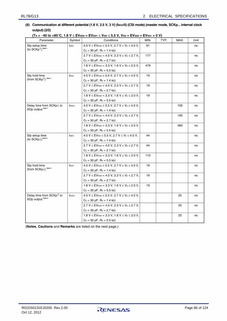
RL78/G13 2. ELECTRICAL SPECIFICATIONS
Page 86 of 124R01DS0131EJ0200 Rev.2.00 Oct 12, 2012
(8) Communication at different potential (1.8 V, 2.5 V, 3 V) (fMCK/4) (CSI mode) (master mode, SCKp... internal clock
output) (2/2)
(TA = −40 to +85°C, 1.8 V ≤ EVDD0 = EVDD1 ≤ VDD ≤ 5.5 V, VSS = EVSS0 = EVSS1 = 0 V) Parameter Symbol Conditions MIN. TYP. MAX. Unit
4.0 V ≤ EVDD0 ≤ 5.5 V, 2.7 V ≤ Vb ≤ 4.0 V,
Cb = 30 pF, Rb = 1.4 kΩ
81 ns
2.7 V ≤ EVDD0 < 4.0 V, 2.3 V ≤ Vb ≤ 2.7 V,
Cb = 30 pF, Rb = 2.7 kΩ
177 ns
SIp setup time (to SCKp↑) Note 1
tSIK1
1.8 V ≤ EVDD0 < 3.3 V, 1.6 V ≤ Vb ≤ 2.0 V,
Cb = 30 pF, Rb = 5.5 kΩ
479 ns
4.0 V ≤ EVDD0 ≤ 5.5 V, 2.7 V ≤ Vb ≤ 4.0 V,
Cb = 30 pF, Rb = 1.4 kΩ
19 ns
2.7 V ≤ EVDD0 < 4.0 V, 2.3 V ≤ Vb ≤ 2.7 V,
Cb = 30 pF, Rb = 2.7 kΩ
19 ns
SIp hold time (from SCKp↑) Note 1
tKSI1
1.8 V ≤ EVDD0 < 3.3 V, 1.6 V ≤ Vb ≤ 2.0 V,
Cb = 30 pF, Rb = 5.5 kΩ
19 ns
4.0 V ≤ EVDD0 ≤ 5.5 V, 2.7 V ≤ Vb ≤ 4.0 V,
Cb = 30 pF, Rb = 1.4 kΩ
100 ns
2.7 V ≤ EVDD0 < 4.0 V, 2.3 V ≤ Vb ≤ 2.7 V,
Cb = 30 pF, Rb = 2.7 kΩ
195 ns
Delay time from SCKp↓ to SOp output Note 1
tKSO1
1.8 V ≤ EVDD0 < 3.3 V, 1.6 V ≤ Vb ≤ 2.0 V,
Cb = 30 pF, Rb = 5.5 kΩ
483 ns
4.0 V ≤ EVDD ≤ 5.5 V, 2.7 V ≤ Vb ≤ 4.0 V,
Cb = 30 pF, Rb = 1.4 kΩ
44 ns
2.7 V ≤ EVDD0 < 4.0 V, 2.3 V ≤ Vb ≤ 2.7 V,
Cb = 30 pF, Rb = 2.7 kΩ
44 ns
SIp setup time (to SCKp↓) Note 2
tSIK1
1.8 V ≤ EVDD0 < 3.3 V, 1.6 V ≤ Vb ≤ 2.0 V,
Cb = 30 pF, Rb = 5.5 kΩ
110 ns
4.0 V ≤ EVDD0 ≤ 5.5 V, 2.7 V ≤ Vb ≤ 4.0 V,
Cb = 30 pF, Rb = 1.4 kΩ
19 ns
2.7 V ≤ EVDD0 < 4.0 V, 2.3 V ≤ Vb ≤ 2.7 V,
Cb = 30 pF, Rb = 2.7 kΩ
19 ns
SIp hold time (from SCKp↓) Note 2
tKSI1
1.8 V ≤ EVDD0 < 3.3 V, 1.6 V ≤ Vb ≤ 2.0 V,
Cb = 30 pF, Rb = 5.5 kΩ
19 ns
4.0 V ≤ EVDD0 ≤ 5.5 V, 2.7 V ≤ Vb ≤ 4.0 V,
Cb = 30 pF, Rb = 1.4 kΩ
25 ns
2.7 V ≤ EVDD0 < 4.0 V, 2.3 V ≤ Vb ≤ 2.7 V,
Cb = 30 pF, Rb = 2.7 kΩ
25 ns
Delay time from SCKp↑ to SOp output Note 2
tKSO1
1.8 V ≤ EVDD0 < 3.3 V, 1.6 V ≤ Vb ≤ 2.0 V,
Cb = 30 pF, Rb = 5.5 kΩ
25 ns
(Notes, Cautions and Remarks are listed on the next page.)

RL78/G13 2. ELECTRICAL SPECIFICATIONS
Page 87 of 124R01DS0131EJ0200 Rev.2.00 Oct 12, 2012
CSI mode connection diagram (during communication at different potential)
Vb
Rb
User's device
<Master>
SCKp
SOp
SCK
SI
SIp SO
Vb
Rb
RL78/G13
Notes 1. When DAPmn = 0 and CKPmn = 0, or DAPmn = 1 and CKPmn = 1.
2. When DAPmn = 0 and CKPmn = 1, or DAPmn = 1 and CKPmn = 0.
Cautions 1. Select the TTL input buffer for the SIp pin and the N-ch open drain output (VDD tolerance
(When 20- to 52-pin products)/EVDD tolerance (When 64- to 128-pin products)) mode for the
SOp pin and SCKp pin by using port input mode register g (PIMg) and port output mode
register g (POMg).
2. Use it with EVDD0 ≥ Vb.
Remarks 1. Rb[Ω]:Communication line (SCKp, SOp) pull-up resistance, Cb[F]: Communication line (SCKp, SOp)
load capacitance, Vb[V]: Communication line voltage
2. p: CSI number (p = 00, 01, 10, 20, 30, 31), m: Unit number , n: Channel number (mn = 00, 01, 02, 10,
12, 13), g: PIM and POM number (g = 0, 1, 4, 5, 8, 14)
3. CSI01 of 48-, 52-, 64-pin products, and CSI11 and CSI21 cannot communicate at different potential.
Use other CSI for communication at different potential.

RL78/G13 2. ELECTRICAL SPECIFICATIONS
Page 88 of 124R01DS0131EJ0200 Rev.2.00 Oct 12, 2012
CSI mode serial transfer timing (master mode) (during communication at different potential)
(When DAPmn = 0 and CKPmn = 0, or DAPmn = 1 and CKPmn = 1.)
SIp Input data
Output dataSOp
tKCY1
tKL1 tKH1
tSIK1 tKSI1
tKSO1
SCKp
CSI mode serial transfer timing (master mode) (during communication at different potential)
(When DAPmn = 0 and CKPmn = 1, or DAPmn = 1 and CKPmn = 0.)
SIp Input data
Output dataSOp
tKCY1
tKL1tKH1
tSIK1 tKSI1
tKSO1
SCKp
Caution Select the TTL input buffer for the SIp pin and the N-ch open drain output (VDD tolerance (When
20- to 52-pin products)/EVDD tolerance (When 64- to 128-pin products)) mode for the SOp pin and
SCKp pin by using port input mode register g (PIMg) and port output mode register g (POMg).
Remarks 1. p: CSI number (p = 00, 01, 10, 20, 30, 31), m: Unit number (m = 00, 01, 02, 10, 12, 13), n: Channel
number (n = 0, 2), g: PIM and POM number (g = 0, 1, 4, 5, 8, 14)
2. CSI01 of 48-, 52-, 64-pin products, and CSI11 and CSI21 cannot communicate at different potential.
Use other CSI for communication at different potential.
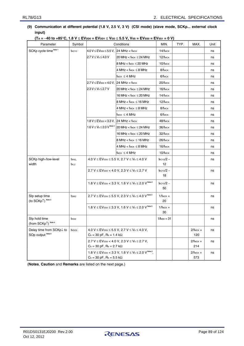
RL78/G13 2. ELECTRICAL SPECIFICATIONS
Page 89 of 124R01DS0131EJ0200 Rev.2.00 Oct 12, 2012
(9) Communication at different potential (1.8 V, 2.5 V, 3 V) (CSI mode) (slave mode, SCKp... external clock
input)
(TA = −40 to +85°C, 1.8 V ≤ EVDD0 = EVDD1 ≤ VDD ≤ 5.5 V, VSS = EVSS0 = EVSS1 = 0 V)
Parameter Symbol Conditions MIN. TYP. MAX. Unit
24 MHz < fMCK 14/fMCK ns
20 MHz < fMCK ≤ 24 MHz 12/fMCK ns
8 MHz < fMCK ≤ 20 MHz 10/fMCK ns
4 MHz < fMCK ≤ 8 MHz 8/fMCK ns
4.0 V ≤ EVDD0 ≤ 5.5 V,
2.7 V ≤ Vb ≤ 4.0 V
fMCK ≤ 4 MHz 6/fMCK ns
24 MHz < fMCK 20/fMCK ns
20 MHz < fMCK ≤ 24 MHz 16/fMCK ns
16 MHz < fMCK ≤ 20 MHz 14/fMCK ns
8 MHz < fMCK ≤ 16 MHz 12/fMCK ns
4 MHz < fMCK ≤ 8 MHz 8/fMCK ns
2.7 V ≤ EVDD0 < 4.0 V,
2.3 V ≤ Vb ≤ 2.7 V
fMCK ≤ 4 MHz 6/fMCK ns
24 MHz < fMCK 48/fMCK ns
20 MHz < fMCK ≤ 24 MHz 36/fMCK ns
16 MHz < fMCK ≤ 20 MHz 32/fMCK ns
8 MHz < fMCK ≤ 16 MHz 26/fMCK ns
4 MHz < fMCK ≤ 8 MHz 16/fMCK ns
SCKp cycle time Note 1 tKCY2
1.8 V ≤ EVDD0 < 3.3 V,
1.6 V ≤ Vb ≤ 2.0 V Note 2
fMCK ≤ 4 MHz 10/fMCK ns
4.0 V ≤ EVDD0 ≤ 5.5 V, 2.7 V ≤ Vb ≤ 4.0 V tKCY2/2 −
12
ns
2.7 V ≤ EVDD0 < 4.0 V, 2.3 V ≤ Vb ≤ 2.7 V tKCY2/2 −
18
ns
SCKp high-/low-level
width
tKH2,
tKL2
1.8 V ≤ EVDD0 < 3.3 V, 1.6 V ≤ Vb ≤ 2.0 V Note 2 tKCY2/2 −
50
ns
2.7 V ≤ EVDD0 ≤ 5.5 V, 2.3 V ≤ Vb ≤ 4.0 V Note 2 1/fMCK +
20
ns SIp setup time
(to SCKp↑) Note 3
tSIK2
1.8 V ≤ EVDD0 ≤ 3.3 V, 1.6 V ≤ Vb ≤ 2.0 V Note 2 1/fMCK +
30
ns
SIp hold time
(from SCKp↑) Note 4
tKSI2 1/fMCK + 31 ns
4.0 V ≤ EVDD0 ≤ 5.5 V, 2.7 V ≤ Vb ≤ 4.0 V,
Cb = 30 pF, Rb = 1.4 kΩ
2/fMCK +
120
ns
2.7 V ≤ EVDD0 < 4.0 V, 2.3 V ≤ Vb ≤ 2.7 V,
Cb = 30 pF, Rb = 2.7 kΩ
2/fMCK +
214
ns
Delay time from SCKp↓ to
SOp output Note 5
tKSO2
1.8 V ≤ EVDD0 < 3.3 V, 1.6 V ≤ Vb ≤ 2.0 V Note 2,
Cb = 30 pF, Rb = 5.5 kΩ
2/fMCK +
573
ns
(Notes, Caution and Remarks are listed on the next page.)

RL78/G13 2. ELECTRICAL SPECIFICATIONS
Page 90 of 124R01DS0131EJ0200 Rev.2.00 Oct 12, 2012
CSI mode connection diagram (during communication at different potential)
User's device
<Slave>
SCKp
SOp
SCK
SI
SIp SO
Vb
Rb
RL78/G13
Notes 1. Transfer rate in the SNOOZE mode : MAX. 1 Mbps
2. Use it with EVDD0 ≥ Vb.
3. When DAPmn = 0 and CKPmn = 0, or DAPmn = 1 and CKPmn = 1. The SIp setup time becomes “to
SCKp↓” when DAPmn = 0 and CKPmn = 1, or DAPmn = 1 and CKPmn = 0.
4. When DAPmn = 0 and CKPmn = 0, or DAPmn = 1 and CKPmn = 1. The SIp hold time becomes “from
SCKp↓” when DAPmn = 0 and CKPmn = 1, or DAPmn = 1 and CKPmn = 0.
5. When DAPmn = 0 and CKPmn = 0, or DAPmn = 1 and CKPmn = 1. The delay time to SOp output
becomes “from SCKp↑” when DAPmn = 0 and CKPmn = 1, or DAPmn = 1 and CKPmn = 0.
Caution Select the TTL input buffer for the SIp pin and SCKp pin and the N-ch open drain output (VDD
tolerance (When 20- to 52-pin products)/EVDD tolerance (When 64- to 128-pin products)) mode for
the SOp pin by using port input mode register g (PIMg) and port output mode register g (POMg).
Remarks 1. Rb[Ω]:Communication line (SOp) pull-up resistance, Cb[F]: Communication line (SOp) load
capacitance, Vb[V]: Communication line voltage
2. p: CSI number (p = 00, 01, 10, 20, 30, 31), m: Unit number (m = 0, 1), n: Channel number (n = 00, 01,
02, 10, 12, 13), g: PIM and POM number (g = 0, 1, 4, 5, 8, 14)
3. fMCK: Serial array unit operation clock frequency
(Operation clock to be set by the CKSmn bit of serial mode register mn (SMRmn).
m: Unit number, n: Channel number (mn = 00, 01, 02, 10, 12, 13))
4. CSI01 of 48-, 52-, 64-pin products, and CSI11 and CSI21 cannot communicate at different potential.
Use other CSI for communication at different potential.

RL78/G13 2. ELECTRICAL SPECIFICATIONS
Page 91 of 124R01DS0131EJ0200 Rev.2.00 Oct 12, 2012
CSI mode serial transfer timing (slave mode) (during communication at different potential)
(When DAPmn = 0 and CKPmn = 0, or DAPmn = 1 and CKPmn = 1.)
SIp Input data
Output dataSOp
tKCY2
tKL2 tKH2
tSIK2 tKSI2
tKSO2
SCKp
CSI mode serial transfer timing (slave mode) (during communication at different potential)
(When DAPmn = 0 and CKPmn = 1, or DAPmn = 1 and CKPmn = 0.)
SIp Input data
Output dataSOp
tKCY2
tKL2tKH2
tSIK2 tKSI2
tKSO2
SCKp
Caution Select the TTL input buffer for the SIp pin and SCKp pin and the N-ch open drain output (VDD
tolerance (When 20- to 52-pin products)/EVDD tolerance (When 64- to 128-pin products)) mode for
the SOp pin by using port input mode register g (PIMg) and port output mode register g (POMg).
Remarks 1. p: CSI number (p = 00, 01, 10, 20, 30, 31), m: Unit number,
n: Channel number (mn = 00, 01, 02, 10, 12. 13), g: PIM and POM number (g = 0, 1, 4, 5, 8, 14)
2. CSI01 of 48-, 52-, 64-pin products, and CSI11 and CSI21 cannot communicate at different potential.
Use other CSI for communication at different potential.

RL78/G13 2. ELECTRICAL SPECIFICATIONS
Page 92 of 124R01DS0131EJ0200 Rev.2.00 Oct 12, 2012
(10) Communication at different potential (1.8 V, 2.5 V, 3 V) (simplified I2C mode) (1/2)
(TA = −40 to +85°C, 1.8 V ≤ EVDD0 = EVDD1 ≤ VDD ≤ 5.5 V, VSS = EVSS0 = EVSS1 = 0 V)
Parameter Symbol Conditions MIN. MAX. Unit
4.0 V ≤ EVDD0 ≤ 5.5 V,
2.7 V ≤ Vb ≤ 4.0 V,
Cb = 50 pF, Rb = 2.7 kΩ
1000 kHz
2.7 V ≤ EVDD0 < 4.0 V,
2.3 V ≤ Vb < 2.7 V,
Cb = 50 pF, Rb = 2.7 kΩ
1000 kHz
4.0 V ≤ EVDD0 ≤ 5.5 V,
2.7 V ≤ Vb ≤ 4.0 V,
Cb = 100 pF, Rb = 2.8 kΩ
400 kHz
2.7 V ≤ EVDD0 < 4.0 V,
2.3 V ≤ Vb < 2.7 V,
Cb = 100 pF, Rb = 2.7 kΩ
400 kHz
SCLr clock frequency fSCL
1.8 V ≤ EVDD0 < 3.3 V,
1.6 V ≤ Vb ≤ 2.0 V Note 1,
Cb = 100 pF, Rb = 5.5 kΩ
300 kHz
4.0 V ≤ EVDD0 ≤ 5.5 V,
2.7 V ≤ Vb ≤ 4.0 V,
Cb = 50 pF, Rb = 2.7 kΩ
475 ns
2.7 V ≤ EVDD0 < 4.0 V,
2.3 V ≤ Vb < 2.7 V,
Cb = 50 pF, Rb = 2.7 kΩ
475 ns
4.0 V ≤ EVDD0 ≤ 5.5 V,
2.7 V ≤ Vb ≤ 4.0 V,
Cb = 100 pF, Rb = 2.8 kΩ
1150 ns
2.7 V ≤ EVDD0 < 4.0 V,
2.3 V ≤ Vb < 2.7 V,
Cb = 100 pF, Rb = 2.7 kΩ
1150 ns
Hold time when SCLr = “L” tLOW
1.8 V ≤ EVDD0 < 3.3 V,
1.6 V ≤ Vb ≤ 2.0 V Note 1,
Cb = 100 pF, Rb = 5.5 kΩ
1550 ns
4.0 V ≤ EVDD0 ≤ 5.5 V,
2.7 V ≤ Vb ≤ 4.0 V,
Cb = 50 pF, Rb = 2.7 kΩ
245 ns
2.7 V ≤ EVDD0 < 4.0 V,
2.3 V ≤ Vb < 2.7 V,
Cb = 50 pF, Rb = 2.7 kΩ
200 ns
4.0 V ≤ EVDD0 ≤ 5.5 V,
2.7 V ≤ Vb ≤ 4.0 V,
Cb = 100 pF, Rb = 2.8 kΩ
675 ns
2.7 V ≤ EVDD0 < 4.0 V,
2.3 V ≤ Vb < 2.7 V,
Cb = 100 pF, Rb = 2.7 kΩ
600 ns
Hold time when SCLr = “H” tHIGH
1.8 V ≤ EVDD0 < 3.3 V,
1.6 V ≤ Vb ≤ 2.0 V Note 1,
Cb = 100 pF, Rb = 5.5 kΩ
610 ns
(Notes, Caution and Remarks are listed on the next page.)

RL78/G13 2. ELECTRICAL SPECIFICATIONS
Page 93 of 124R01DS0131EJ0200 Rev.2.00 Oct 12, 2012
(10) Communication at different potential (1.8 V, 2.5 V, 3 V) (simplified I2C mode) (2/2)
(TA = −40 to +85°C, 1.8 V ≤ EVDD0 = EVDD1 ≤ VDD ≤ 5.5 V, VSS = EVSS0 = EVSS1 = 0 V) Parameter Symbol Conditions MIN. MAX. Unit
4.0 V ≤ EVDD0 ≤ 5.5 V, 2.7 V ≤ Vb ≤ 4.0 V, Cb = 50 pF, Rb = 2.7 kΩ
1/fMCK + 135
Note 2 ns
2.7 V ≤ EVDD0 < 4.0 V, 2.3 V ≤ Vb < 2.7 V, Cb = 50 pF, Rb = 2.7 kΩ
1/fMCK + 135
Note 2 ns
4.0 V ≤ EVDD0 ≤ 5.5 V, 2.7 V ≤ Vb ≤ 4.0 V, Cb = 100 pF, Rb = 2.8 kΩ
1/fMCK + 190
Note 2 ns
2.7 V ≤ EVDD0 < 4.0 V, 2.3 V ≤ Vb < 2.7 V, Cb = 100 pF, Rb = 2.7 kΩ
1/fMCK + 190
Note 2 ns
Data setup time (reception) tSU:DAT
1.8 V ≤ EVDD0 < 3.3 V, 1.6 V ≤ Vb ≤ 2.0 V Notes 1, Cb = 100 pF, Rb = 5.5 kΩ
1/fMCK + 190
Note 2 ns
4.0 V ≤ EVDD0 ≤ 5.5 V, 2.7 V ≤ Vb ≤ 4.0 V, Cb = 50 pF, Rb = 2.7 kΩ
0 305 ns
2.7 V ≤ EVDD0 < 4.0 V, 2.3 V ≤ Vb < 2.7 V, Cb = 50 pF, Rb = 2.7 kΩ
0 305 ns
4.0 V ≤ EVDD0 ≤ 5.5 V, 2.7 V ≤ Vb ≤ 4.0 V, Cb = 100 pF, Rb = 2.8 kΩ
0 355 ns
2.7 V ≤ EVDD0 < 4.0 V, 2.3 V ≤ Vb < 2.7 V, Cb = 100 pF, Rb = 2.7 kΩ
0 355 ns
Data hold time (transmission) tHD:DAT
1.8 V ≤ EVDD0 < 3.3 V, 1.6 V ≤ Vb ≤ 2.0 V Note 1, Cb = 100 pF, Rb = 5.5 kΩ
0 405 ns
Notes 1. Use it with EVDD0 ≥ Vb.
2. Set the fMCK value to keep the hold time of SCLr = "L" and SCLr = "H".
Caution Select the TTL input buffer and the N-ch open drain output (VDD tolerance (When 20- to 52-pin
products)/EVDD tolerance (When 64- to 128-pin products)) mode for the SDAr pin and the N-ch
open drain output (VDD tolerance (When 20- to 52-pin products)/EVDD tolerance (When 64- to 128-
pin products)) mode for the SCLr pin by using port input mode register g (PIMg) and port output
mode register g (POMg).
(Remarks is listed on the next page.)

RL78/G13 2. ELECTRICAL SPECIFICATIONS
Page 94 of 124R01DS0131EJ0200 Rev.2.00 Oct 12, 2012
Simplified I2C mode connection diagram (during communication at different potential)
User's device
SDAr
SCLr
SDA
SCL
Vb
Rb
Vb
Rb
RL78/G13
Simplified I2C mode serial transfer timing (during communication at different potential)
SDAr
tLOW tHIGH
tHD:DAT
SCLr
tSU:DAT
1/fSCL
Caution Select the TTL input buffer and the N-ch open drain output (VDD tolerance (When 20- to 52-pin
products)/EVDD tolerance (When 64- to 128-pin products)) mode for the SDAr pin and the N-ch
open drain output (VDD tolerance (When 20- to 52-pin products)/EVDD tolerance (When 64- to 128-
pin products)) mode for the SCLr pin by using port input mode register g (PIMg) and port output
mode register g (POMg).
Remarks 1. Rb[Ω]:Communication line (SDAr, SCLr) pull-up resistance, Cb[F]: Communication line (SDAr, SCLr)
load capacitance, Vb[V]: Communication line voltage
2. r: IIC number (r = 00, 01, 10, 20, 30, 31), g: PIM, POM number (g = 0, 1, 4, 5, 8, 14)
3. fMCK: Serial array unit operation clock frequency
(Operation clock to be set by the CKSmn bit of serial mode register mn (SMRmn). m: Unit number, n:
Channel number (mn = 00, 01, 02, 10, 12, 13)

RL78/G13 2. ELECTRICAL SPECIFICATIONS
Page 95 of 124R01DS0131EJ0200 Rev.2.00 Oct 12, 2012
2.5.2 Serial interface IICA
(TA = −40 to +85°C, 1.6 V ≤ EVDD0 = EVDD1 ≤ VDD ≤ 5.5 V, VSS = EVSS0 = EVSS1 = 0 V)
Standard
Mode
Fast Mode Fast Mode
Plus
Parameter Symbol Conditions
MIN. MAX. MIN. MAX. MIN. MAX.
Unit
Fast mode plus:
fCLK ≥ 10 MHz 2.7 V ≤ EVDD0 ≤ 5.5 V 0 1000 kHz
Fast mode:
fCLK ≥ 3.5 MHz 1.8 V ≤ EVDD0 ≤ 5.5 V 0 400 kHz
SCLA0 clock frequency fSCL
Normal mode:
fCLK ≥ 1 MHz 1.6 V ≤ EVDD0 ≤ 5.5 V 0 100 kHz
Setup time of restart condition tSU:STA 4.7 0.6 0.26 μs
Hold timeNote 1 tHD:STA 4.0 0.6 0.26 μs
Hold time when SCLA0 = “L” tLOW 4.7 1.3 0.5 μs
Hold time when SCLA0 = “H” tHIGH 4.0 0.6 0.26 μs
Data setup time (reception) tSU:DAT 250 100 50 ns
Data hold time (transmission)Note 2 tHD:DAT 0 3.45 0 0.9 0 0.45 μs
Setup time of stop condition tSU:STO 4.0 0.6 0.26 μs
Bus-free time tBUF 4.7 1.3 0.5 μs
Notes 1. The first clock pulse is generated after this period when the start/restart condition is detected. 2. The maximum value (MAX.) of tHD:DAT is during normal transfer and a wait state is inserted in the ACK
(acknowledge) timing.
Remark The maximum value of Cb (communication line capacitance) and the value of Rb (communication line
pull-up resistor) at that time in each mode are as follows. Standard mode: Cb = 400 pF, Rb = 2.7 kΩ Fast mode: Cb = 320 pF, Rb = 1.1 kΩ Fast mode plus: Cb = 120 pF, Rb = 1.1 kΩ
IICA serial transfer timing
tLOW
tLOW
tHIGH
tHD:STA
Stop condition
Start condition
Restart condition
Stop condition
tSU:DAT
tSU:STA tSU:STOtHD:STAtHD:DAT
SCL0
SDA0

RL78/G13 2. ELECTRICAL SPECIFICATIONS
Page 96 of 124R01DS0131EJ0200 Rev.2.00 Oct 12, 2012
2.5.3 On-chip debug (UART)
(TA = −40 to +85°C, 1.8 V ≤ EVDD0 = EVDD1 ≤ VDD ≤ 5.5 V, VSS = EVSS0 = EVSS1 = 0 V)
Parameter Symbol Conditions MIN. TYP. MAX. Unit
Transfer rate 115.2 k 1 M bps
2.6 Analog Characteristics
2.6.1 A/D converter characteristics (1) When AVREF (+) = AVREFP/ANI0 (ADREFP1 = 0, ADREFP0 = 1), AVREF (−) = AVREFM/ANI1 (ADREFM = 1), target
ANI pin : ANI2 to ANI14
(TA = −40 to +85°C, 1.6 V ≤ EVDD0 = EVDD1 ≤ VDD ≤ 5.5 V, VSS = EVSS0 = EVSS1 = 0 V, Reference voltage (+) =
AVREFP, Reference voltage (−) = AVREFM = 0 V)
Parameter Symbol Conditions MIN. TYP. MAX. Unit
Resolution RES 8 10 bit
1.8 V ≤ VDD ≤ 5.5 V 1.2 ±3.5 LSB Overall errorNote 1 AINL 10-bit resolution
AVREFP = VDD 1.6 V ≤ VDD ≤ 5.5 V 1.2 ±7.0 LSB
3.6 V ≤ VDD ≤ 5.5 V 2.125 39 μs
2.7 V ≤ VDD ≤ 5.5 V 3.1875 39 μs
1.8 V ≤ VDD ≤ 5.5 V 17 39 μs
Conversion time tCONV 10-bit resolution
AVREFP = VDD
1.6 V ≤ VDD ≤ 5.5 V 57 95 μs
1.8 V ≤ VDD ≤ 5.5 V ±0.25 %FSRZero-scale errorNotes 1, 2 EZS 10-bit resolution AVREFP = VDD
1.6 V ≤ VDD ≤ 5.5 V ±0.50 %FSR
1.8 V ≤ VDD ≤ 5.5 V ±0.25 %FSRFull-scale errorNotes 1, 2 EFS 10-bit resolution AVREFP = VDD
1.6 V ≤ VDD ≤ 5.5 V ±0.50 %FSR
1.8 V ≤ VDD ≤ 5.5 V ±2.5 LSB Integral linearity errorNote 1 ILE 10-bit resolution
AVREFP = VDD 1.6 V ≤ VDD ≤ 5.5 V ±5.0 LSB
1.8 V ≤ VDD ≤ 5.5 V ±1.5 LSB Differential linearity error Note 1 DLE 10-bit resolution
AVREFP = VDD 1.6 V ≤ VDD ≤ 5.5 V ±2.0 LSB
Reference voltage (+) AVREFP 1.6 VDD V
VAIN 0 AVREFP V Analog input voltage
VBGR Select interanal reference voltage output
2.4 V ≤ VDD ≤ 5.5 V, HS (high-speed main) mode
1.38 1.45 1.5 V
Notes 1. Excludes quantization error (±1/2 LSB).
2. This value is indicated as a ratio (%FSR) to the full-scale value.
<R>

RL78/G13 2. ELECTRICAL SPECIFICATIONS
Page 97 of 124R01DS0131EJ0200 Rev.2.00 Oct 12, 2012
(2) When AVREF (+) = AVREFP/ANI0 (ADREFP1 = 0, ADREFP0 = 1), AVREF (−) = AVREFM/ANI1 (ADREFM = 1), target
ANI pin : ANI16 to ANI26
(TA = −40 to +85°C, 1.6 V ≤ EVDD0 = EVDD1 ≤ VDD ≤ 5.5 V, VSS = EVSS0 = EVSS1 = 0 V, Reference voltage (+) =
AVREFP, Reference voltage (−) = AVREFM)
Parameter Symbol Conditions MIN. TYP. MAX. Unit
Resolution RES 8 10 bit
1.8 V ≤ VDD ≤ 5.5 V 1.2 ±5.0 LSB Overall errorNote 1 AINL 10-bit resolution
AVREFP = VDD 1.6 V ≤ VDD ≤ 5.5 V 1.2 ±8.5 LSB
3.6 V ≤ VDD ≤ 5.5 V 2.125 39 μs
2.7 V ≤ VDD ≤ 5.5 V 3.1875 39 μs
1.8 V ≤ VDD ≤ 5.5 V 17 39 μs
Conversion time tCONV 10-bit resolution
AVREFP = VDD
1.6 V ≤ VDD ≤ 5.5 V 57 95 μs
1.8 V ≤ VDD ≤ 5.5 V ±0.35 %FSRZero-scale errorNotes 1, 2 EZS 10-bit resolution AVREFP = VDD
1.6 V ≤ VDD ≤ 5.5 V ±0.60 %FSR
1.8 V ≤ VDD ≤ 5.5 V ±0.35 %FSRFull-scale errorNotes 1, 2 EFS 10-bit resolution AVREFP = VDD
1.6 V ≤ VDD ≤ 5.5 V ±0.60 %FSR
1.8 V ≤ VDD ≤ 5.5 V ±3.5 LSB Integral linearity errorNote 1 ILE 10-bit resolution
AVREFP = VDD 1.6 V ≤ VDD ≤ 5.5 V ±6.0 LSB
1.8 V ≤ VDD ≤ 5.5 V ±2.0 LSB Differential linearity error Note 1 DLE 10-bit resolution
AVREFP = VDD 1.6 V ≤ VDD ≤ 5.5 V ±2.5 LSB
Reference voltage (+) AVREFP 1.6 VDD V
VAIN 0 AVREFP
and
EVDD0
V Analog input voltage
VBGR Select interanal reference voltage output
2.4 V ≤ VDD ≤ 5.5 V, HS (high-speed main) mode
1.38 1.45 1.5 V
Notes 1. Excludes quantization error (±1/2 LSB).
2. This value is indicated as a ratio (%FSR) to the full-scale value.
<R>

RL78/G13 2. ELECTRICAL SPECIFICATIONS
Page 98 of 124R01DS0131EJ0200 Rev.2.00 Oct 12, 2012
(3) When AVREF (+) = VDD (ADREFP1 = 0, ADREFP0 = 0), AVREF (−) = VSS (ADREFM = 0), target ANI pin : ANI0 to
ANI14, ANI16 to ANI26
(TA = −40 to +85°C, 1.6 V ≤ EVDD0 = EVDD1 ≤ VDD ≤ 5.5 V, VSS = EVSS0 = EVSS1 = 0 V, Reference voltage (+) = VDD,
Reference voltage (−) = VSS)
Parameter Symbol Conditions MIN. TYP. MAX. Unit
Resolution RES 8 10 bit
1.8 V ≤ VDD ≤ 5.5 V 1.2 ±7.0 LSB Overall errorNote 1 AINL 10-bit resolution
1.6 V ≤ VDD ≤ 5.5 V 1.2 ±10.5 LSB
3.6 V ≤ VDD ≤ 5.5 V 2.125 39 μs
2.7 V ≤ VDD ≤ 5.5 V 3.1875 39 μs
1.8 V ≤ VDD ≤ 5.5 V 17 39 μs
Conversion time tCONV 10-bit resolution
1.6 V ≤ VDD ≤ 5.5 V 57 95 μs
1.8 V ≤ VDD ≤ 5.5 V ±0.60 %FSRZero-scale errorNotes 1, 2 EZS 10-bit resolution
1.6 V ≤ VDD ≤ 5.5 V ±0.85 %FSR
1.8 V ≤ VDD ≤ 5.5 V ±0.60 %FSRFull-scale errorNotes 1, 2 EFS 10-bit resolution
1.6 V ≤ VDD ≤ 5.5 V ±0.85 %FSR
1.8 V ≤ VDD ≤ 5.5 V ±4.0 LSB Integral linearity errorNote 1 ILE 10-bit resolution
1.6 V ≤ VDD ≤ 5.5 V ±6.5 LSB
1.8 V ≤ VDD ≤ 5.5 V ±2.0 LSB Differential linearity error Note 1 DLE 10-bit resolution
1.6 V ≤ VDD ≤ 5.5 V ±2.5 LSB
ANI0 to ANI14 0 VDD V VAIN
ANI16 to ANI26 0 EVDD0 V
Analog input voltage
VBGR Select interanal reference voltage output,
2.4 V ≤ VDD ≤ 5.5 V, HS (high-speed main) mode
1.38 1.45 1.5 V
Notes 1. Excludes quantization error (±1/2 LSB).
2. This value is indicated as a ratio (%FSR) to the full-scale value.
<R>

RL78/G13 2. ELECTRICAL SPECIFICATIONS
Page 99 of 124R01DS0131EJ0200 Rev.2.00 Oct 12, 2012
(4) When AVREF (+) = Internal reference voltage (ADREFP1 = 1, ADREFP0 = 0), AVREF (−) = AVREFM/ANI1
(ADREFM = 1), target ANI pin : ANI0 to ANI14, ANI16 to ANI26
(TA = −40 to +85°C, 2.4 V ≤ VDD ≤ 5.5 V, VSS = EVSS0 = EVSS1 = 0 V, Reference voltage (+) = VBGR, Reference
voltage (−) = AVREFM = 0 V, HS (high-speed main) mode)
Parameter Symbol Conditions MIN. TYP. MAX. Unit
Resolution RES 8 bit
Conversion time tCONV 8-bit resolution 2.4 V ≤ VDD ≤ 5.5 V 17 39 μs
Zero-scale errorNotes 1, 2 EZS 8-bit resolution 2.4 V ≤ VDD ≤ 5.5 V ±0.60 %FSR
Integral linearity errorNote 1 ILE 8-bit resolution 2.4 V ≤ VDD ≤ 5.5 V ±2.0 LSB
Differential linearity error Note 1 DLE 8-bit resolution 2.4 V ≤ VDD ≤ 5.5 V ±1.0 LSB
Reference voltage (+) VBGR 1.38 1.45 1.5 V
Analog input voltage VAIN 0 VBGR V
Notes 1. Excludes quantization error (±1/2 LSB).
2. This value is indicated as a ratio (%FSR) to the full-scale value.

RL78/G13 2. ELECTRICAL SPECIFICATIONS
Page 100 of 124R01DS0131EJ0200 Rev.2.00 Oct 12, 2012
2.6.2 Temperature sensor characteristics
(TA = −40 to +85°C, 2.4 V ≤ VDD ≤ 5.5 V, VSS = EVSS0 = EVSS1 = 0 V, HS (high-speed main) mode)
Parameter Symbol Conditions MIN. TYP. MAX. Unit
Temperature sensor output voltage VTMPS25 Setting ADS register = 80H, TA = +25°C 1.05 V
Internal reference voltage VCONST Setting ADS register = 81H 1.38 1.45 1.5 V
Temperature coefficient FVTMPS Temperature sensor that depends on the
temperature
−3.6 mV/°C
Operation stabilization wait time tAMP 5 μs
2.6.3 POR circuit characteristics
(TA = −40 to +85°C, VSS = 0 V)
Parameter Symbol Conditions MIN. TYP. MAX. Unit
VPOR Power supply rise time 1.48 1.51 1.54 V Detection voltage
VPDR Power supply fall time 1.47 1.50 1.53 V
Minimum pulse width TPW 300 μs
Detection delay time 350 μs
<R>

RL78/G13 2. ELECTRICAL SPECIFICATIONS
Page 101 of 124R01DS0131EJ0200 Rev.2.00 Oct 12, 2012
2.6.4 LVD circuit characteristics
LVD Detection Voltage of Reset Mode and Interrupt Mode
(TA = −40 to +85°C, VPDR ≤ EVDD0 = EVDD1 ≤ VDD ≤ 5.5 V, VSS = EVSS0 = EVSS1 = 0 V)
Parameter Symbol Conditions MIN. TYP. MAX. Unit
Power supply rise time 3.98 4.06 4.14 V VLVD0
Power supply fall time 3.90 3.98 4.06 V
Power supply rise time 3.68 3.75 3.82 V VLVD1
Power supply fall time 3.60 3.67 3.74 V
Power supply rise time 3.07 3.13 3.19 V VLVD2
Power supply fall time 3.00 3.06 3.12 V
Power supply rise time 2.96 3.02 3.08 V VLVD3
Power supply fall time 2.90 2.96 3.02 V
Power supply rise time 2.86 2.92 2.97 V VLVD4
Power supply fall time 2.80 2.86 2.91 V
Power supply rise time 2.76 2.81 2.87 V VLVD5
Power supply fall time 2.70 2.75 2.81 V
Power supply rise time 2.66 2.71 2.76 V VLVD6
Power supply fall time 2.60 2.65 2.70 V
Power supply rise time 2.56 2.61 2.66 V VLVD7
Power supply fall time 2.50 2.55 2.60 V
Power supply rise time 2.45 2.50 2.55 V VLVD8
Power supply fall time 2.40 2.45 2.50 V
Power supply rise time 2.05 2.09 2.13 V VLVD9
Power supply fall time 2.00 2.04 2.08 V
Power supply rise time 1.94 1.98 2.02 V VLVD10
Power supply fall time 1.90 1.94 1.98 V
Power supply rise time 1.84 1.88 1.91 V VLVD11
Power supply fall time 1.80 1.84 1.87 V
Power supply rise time 1.74 1.77 1.81 V VLVD12
Power supply fall time 1.70 1.73 1.77 V
Power supply rise time 1.64 1.67 1.70 V
Detection
voltage
Supply voltage level
VLVD13
Power supply fall time 1.60 1.63 1.66 V
Minimum pulse width tLW 300 μs
Detection delay time 300 μs

RL78/G13 2. ELECTRICAL SPECIFICATIONS
Page 102 of 124R01DS0131EJ0200 Rev.2.00 Oct 12, 2012
LVD Detection Voltage of Interrupt & Reset Mode
(TA = −40 to +85°C, VPDR ≤ EVDD0 = EVDD1 ≤ VDD ≤ 5.5 V, VSS = EVSS0 = EVSS1 = 0 V)
Parameter Symbol Conditions MIN. TYP. MAX. Unit
VLVD13 VPOC2, VPOC1, VPOC0 = 0, 0, 0, falling reset voltage: 1.6 V 1.60 1.63 1.66 V
Rising release reset voltage 1.74 1.77 1.81 V VLVD12 LVIS1, LVIS0 = 1, 0
(+0.1 V) Falling interrupt voltage 1.70 1.73 1.77 V
Rising release reset voltage 1.84 1.88 1.91 V VLVD11 LVIS1, LVIS0 = 0, 1
(+0.2 V) Falling interrupt voltage 1.80 1.84 1.87 V
Rising release reset voltage 2.86 2.92 2.97 V VLVD4
LVIS1, LVIS0 = 0, 0
(+1.2 V) Falling interrupt voltage 2.80 2.86 2.91 V
VLVD11 VPOC2, VPOC1, VPOC0 = 0, 0, 1, falling reset voltage: 1.8 V 1.80 1.84 1.87 V
Rising release reset voltage 1.94 1.98 2.02 V VLVD10 LVIS1, LVIS0 = 1, 0
(+0.1 V) Falling interrupt voltage 1.90 1.94 1.98 V
Rising release reset voltage 2.05 2.09 2.13 V VLVD9 LVIS1, LVIS0 = 0, 1
(+0.2 V) Falling interrupt voltage 2.00 2.04 2.08 V
Rising release reset voltage 3.07 3.13 3.19 V VLVD2
LVIS1, LVIS0 = 0, 0
(+1.2 V) Falling interrupt voltage 3.00 3.06 3.12 V
VLVD8 VPOC2, VPOC1, VPOC0 = 0, 1, 0, falling reset voltage: 2.4 V 2.40 2.45 2.50 V
Rising release reset voltage 2.56 2.61 2.66 V VLVD7 LVIS1, LVIS0 = 1, 0
(+0.1 V) Falling interrupt voltage 2.50 2.55 2.60 V
Rising release reset voltage 2.66 2.71 2.76 V VLVD6 LVIS1, LVIS0 = 0, 1
(+0.2 V) Falling interrupt voltage 2.60 2.65 2.70 V
Rising release reset voltage 3.68 3.75 3.82 V VLVD1
LVIS1, LVIS0 = 0, 0
(+1.2 V) Falling interrupt voltage 3.60 3.67 3.74 V
VLVD5 VPOC2, VPOC1, VPOC0 = 0, 1, 1, falling reset voltage: 2.7 V 2.70 2.75 2.81 V
Rising release reset voltage 2.86 2.92 2.97 V VLVD4 LVIS1, LVIS0 = 1, 0
(+0.1 V) Falling interrupt voltage 2.80 2.86 2.91 V
Rising release reset voltage 2.96 3.02 3.08 V VLVD3 LVIS1, LVIS0 = 0, 1
(+0.2 V) Falling interrupt voltage 2.90 2.96 3.02 V
Rising release reset voltage 3.98 4.06 4.14 V
Interrupt and reset
mode
VLVD0
LVIS1, LVIS0 = 0, 0
(+1.2 V) Falling interrupt voltage 3.90 3.98 4.06 V

RL78/G13 2. ELECTRICAL SPECIFICATIONS
Page 103 of 124R01DS0131EJ0200 Rev.2.00 Oct 12, 2012
Supply Voltage Rise Time (TA = −40 to +85°C, VSS = 0 V)
Parameter Symbol Conditions MIN. TYP. MAX. Unit
Maximum time to rise to
1.6 V (VDD (MIN.))Note
(VDD: 0 V → 1.6 V)
tPUP1 When RESET input is not used 3.2 ms
Note Make sure to raise the power supply in a shorter time than this.
Supply Voltage Rise Time Timing
• When RESET pin input is not used Supply voltage
(VDD)
Time
1.6 V
0 V
POR internalsignal
tPUP1

RL78/G13 2. ELECTRICAL SPECIFICATIONS
Page 104 of 124R01DS0131EJ0200 Rev.2.00 Oct 12, 2012
2.7 Data Memory STOP Mode Low Supply Voltage Data Retention Characteristics
(TA = −40 to +85°C)
Parameter Symbol Conditions MIN. TYP. MAX. Unit
Data retention supply voltage VDDDR 1.47Note 5.5 V
Note The value depends on the POR detection voltage. When the voltage drops, the data is retained before a
POR reset is effected, but data is not retained when a POR reset is effected.
VDD
STOP instruction execution
Standby release signal(interrupt request)
STOP mode
Data retention mode
VDDDR
Operation mode
2.8 Flash Memory Programming Characteristics
(TA = −40 to +85°C, 1.8 V ≤ EVDD0 = EVDD1 ≤ VDD ≤ 5.5 V, VSS = EVSS0 = EVSS1 = 0 V)
Parameter Symbol Conditions MIN. TYP. MAX. Unit
CPU/peripheral hardware clock
frequency
fCLK 1.8 V ≤ VDD ≤ 5.5 V 1 32 MHz
Number of code flash rewrites Notes 1, 2, 3
Retained for 20 years TA = 85°C Note 3 1,000
Retained for 1 years TA = 25°C Note 3 1,000,000
Retained for 5 years TA = 85°C Note 3 100,000
Number of data flash rewrites Notes 1, 2, 3
Cerwr
Retained for 20 years TA = 85°C Note 3 10,000
Times
Notes 1. 1 erase + 1 write after the erase is regarded as 1 rewrite.
The retaining years are until next rewrite after the rewrite.
2. When using flash memory programmer and Renesas Electronics self programming library
3. These are the characteristics of the flash memory and the results obtained from reliability testing by
Renesas.
<R>
<R>
<R>
<R>

RL78/G13 2. ELECTRICAL SPECIFICATIONS
Page 105 of 124R01DS0131EJ0200 Rev.2.00 Oct 12, 2012
2.9 Timing Specs for Switching Flash Memory Programming Modes
Parameter Symbol Conditions MIN. TYP. MAX. Unit
How long from when a pin reset
ends until the initial communication
settings are specified
tSUINIT POR and LVD reset must end before the pin
reset ends.
100 ms
How long from when the TOOL0
pin is placed at the low level until a
pin reset ends
tSU POR and LVD reset must end before the pin
reset ends.
10 μ s
How long the TOOL0 pin must be
kept at the low level after a reset
ends
(except soft processing time)
tHD POR and LVD reset must end before the pin
reset ends.
1 ms
RESET
TOOL0
<1> <2> <3>
tSUINIT
tHD+soft processing
time
tSU
<4>
00H reception(TOOLRxD, TOOLTxD mode)
<1> The low level is input to the TOOL0 pin.
<2> The pins reset ends (POR and LVD reset must end before the pin reset ends.).
<3> The TOOL0 pin is set to the high level.
<4> Setting of the flash memory programming mode by UART reception and complete
the baud rate setting.
Remark tSUINIT: The segment shows that it is necessary to finish specifying the initial communication settings
within 100 ms from when the resets end.
tSU: How long from when the TOOL0 pin is placed at the low level until a pin reset ends (MIN. 10 μ s)
tHD: How long to keep the TOOL0 pin at the low level from when the external and internal resets
end (except soft processing time)

RL78/G13 3 PACKAGE DRAWINGS
Page 106 of 124R01DS0131EJ0200 Rev.2.00 Oct 12, 2012
3. PACKAGE DRAWINGS
3.1 20-pin products
R5F1006AASP, R5F1006CASP, R5F1006DASP, R5F1006EASP
R5F1016AASP, R5F1016CASP, R5F1016DASP, R5F1016EASP
R5F1006ADSP, R5F1006CDSP, R5F1006DDSP, R5F1006EDSP
R5F1016ADSP, R5F1016CDSP, R5F1016DDSP, R5F1016EDSP
JEITA Package Code RENESAS Code Previous Code MASS (TYP.) [g]
P-LSSOP20-0300-0.65 PLSP0020JC-A S20MC-65-5A4-3 0.12
N S
C
D M M
PL
U
T
G
F
E
B
K
J
detail of lead end
S
20 11
1 10
A
H
I
ITEM
B
C
I
L
M
N
A
K
D
E
F
G
H
J
P
T
MILLIMETERS
0.65 (T.P.)
0.475 MAX.
0.13
0.5
6.1±0.2
0.10
6.65±0.15
0.17±0.03
0.1±0.05
0.24
1.3±0.1
8.1±0.2
1.2
+0.08−0.07
1.0±0.2
3°+5°−3°
0.25
0.6±0.15U
NOTE
Each lead centerline is located within 0.13 mm ofits true position (T.P.) at maximum material condition.
2012 Renesas Electronics Corporation. All rights reserved.

RL78/G13 3 PACKAGE DRAWINGS
Page 107 of 124R01DS0131EJ0200 Rev.2.00 Oct 12, 2012
3.2 24-pin products
R5F1007AANA, R5F1007CANA, R5F1007DANA, R5F1007EANA
R5F1017AANA, R5F1017CANA, R5F1017DANA, R5F1017EANA
R5F1007ADNA, R5F1007CDNA, R5F1007DDNA, R5F1007EDNA
R5F1017ADNA, R5F1017CDNA, R5F1017DDNA, R5F1017EDNA
2012 Renesas Electronics Corporation. All rights reserved.
Sy
eLp
Sxb A BM
A
D
E
18
12
13
6
7
1
24
A
S
B
A
D
E
A
e
Lp
x
y
4.00 0.05
0.50
0.05
0.05
±
4.00 0.05±
0.75 0.05±
0.40 0.10±
S
D2
E2
(UNIT:mm)
ITEM DIMENSIONS
19
DETAIL OF A PART
EXPOSED DIE PAD
ITEMD2 E2
A
MIN NOM MAX
2.45 2.50EXPOSEDDIE PADVARIATIONS
2.55
MIN NOM MAX
2.45 2.50 2.55
b 0.25 0.05+0.07−
JEITA Package Code RENESAS Code Previous Code MASS (TYP.) [g]
P-HWQFN24-4x4-0.50 PWQN0024KE-A P24K8-50-CAB-1 0.04

RL78/G13 3 PACKAGE DRAWINGS
Page 108 of 124R01DS0131EJ0200 Rev.2.00 Oct 12, 2012
3.3 25-pin products
R5F1008AALA, R5F1008CALA, R5F1008DALA, R5F1008EALA
R5F1018AALA, R5F1018CALA, R5F1018DALA, R5F1018EALA
R5F1008ADLA, R5F1008CDLA, R5F1008DDLA, R5F1008EDLA
R5F1018ADLA, R5F1018CDLA, R5F1018DDLA, R5F1018EDLA
JEITA Package Code RENESAS Code Previous Code MASS (TYP.) [g]
P-WFLGA25-3x3-0.50 PWLG0025KA-A P25FC-50-2N2-2 0.01
(APERTURE OFSOLDER RESIST)
ITEM DIMENSIONS
D
E
w
e
A
b
x
y
y1
ZD
ZE
3.00±0.10
3.00±0.10
0.05
0.20
0.69±0.07
0.08
0.50
0.24±0.05
(UNIT:mm)
0.20
0.50
0.50
S
y1 S A
S
DETAIL OF C PART
y
Sx21x b A BM
e
b
0.34±0.05
0.43±0.05
0.50±0.050.365±0.05
R0.17±0.05
R0.165±0.05
R0.215±0.05
0.365±0.05
0.50±0.05
0.33±0.05
0.43±0.05
Sw B
ZD
ZE
INDEX MARK
B
C
A
Sw AD
E 2.27
2.27
DETAIL OF D PART
D
1
2
E D C B A
3
4
5
(LAND PAD)
R0.12±0.05 0.33±0.05
INDEX MARK
2012 Renesas Electronics Corporation. All rights reserved.

RL78/G13 3 PACKAGE DRAWINGS
Page 109 of 124R01DS0131EJ0200 Rev.2.00 Oct 12, 2012
3.4 30-pin products
R5F100AAASP, R5F100ACASP, R5F100ADASP, R5F100AEASP, R5F100AFASP, R5F100AGASP
R5F101AAASP, R5F101ACASP, R5F101ADASP, R5F101AEASP, R5F101AFASP, R5F101AGASP
R5F100AADSP, R5F100ACDSP, R5F100ADDSP, R5F100AEDSP, R5F100AFDSP, R5F100AGDSP
R5F101AADSP, R5F101ACDSP, R5F101ADDSP, R5F101AEDSP, R5F101AFDSP, R5F101AGDSP
JEITA Package Code RENESAS Code Previous Code MASS (TYP.) [g]
P-LSSOP30-0300-0.65 PLSP0030JB-B S30MC-65-5A4-3 0.18
S
S
H
J
T
I
G
D
E
F
C B
K
PL
U
NITEM
B
C
I
L
M
N
A
K
D
E
F
G
H
J
P
30 16
1 15
A
detail of lead end
MM
T
MILLIMETERS
0.65 (T.P.)
0.45 MAX.
0.13
0.5
6.1±0.2
0.10
9.85±0.15
0.17±0.03
0.1±0.05
0.24
1.3±0.1
8.1±0.2
1.2
+0.08−0.07
1.0±0.2
3°+5°−3°
0.25
0.6±0.15U
NOTE
Each lead centerline is located within 0.13 mm ofits true position (T.P.) at maximum material condition.
2012 Renesas Electronics Corporation. All rights reserved.

RL78/G13 3 PACKAGE DRAWINGS
Page 110 of 124R01DS0131EJ0200 Rev.2.00 Oct 12, 2012
3.5 32-pin products
R5F100BAANA, R5F100BCANA, R5F100BDANA, R5F100BEANA, R5F100BFANA, R5F100BGANA
R5F101BAANA, R5F101BCANA, R5F101BDANA, R5F101BEANA, R5F101BFANA, R5F101BGANA
R5F100BADNA, R5F100BCDNA, R5F100BDDNA, R5F100BEDNA, R5F100BFDNA, R5F100BGDNA
R5F101BADNA, R5F101BCDNA, R5F101BDDNA, R5F101BEDNA, R5F101BFDNA, R5F101BGDNA
2012 Renesas Electronics Corporation. All rights reserved.
Sy
eLp
Sxb A BM
A
D
E
24
16
17
8
9
1
32
A
S
B
A
D
E
A
b
e
Lp
x
y
5.00 0.05
0.50
0.05
0.05
±
5.00 0.05±
0.75 0.05±
0.25 0.05+0.07
0.40 0.10±
S
D2
E2
(UNIT:mm)
ITEM DIMENSIONS
25
DETAIL OF A PART
−EXPOSED DIE PAD
ITEMD2 E2
A
MIN NOM MAX
3.45 3.50EXPOSEDDIE PADVARIATIONS
3.55
MIN NOM MAX
3.45 3.50 3.55
JEITA Package Code RENESAS Code Previous Code MASS (TYP.) [g]
P-HWQFN32-5x5-0.50 PWQN0032KB-A P32K8-50-3B4-3 0.06

RL78/G13 3 PACKAGE DRAWINGS
Page 111 of 124R01DS0131EJ0200 Rev.2.00 Oct 12, 2012
3.6 36-pin products
R5F100CAALA, R5F100CCALA, R5F100CDALA, R5F100CEALA, R5F100CFALA, R5F100CGALA
R5F101CAALA, R5F101CCALA, R5F101CDALA, R5F101CEALA, R5F101CFALA, R5F101CGALA
R5F100CADLA, R5F100CCDLA, R5F100CDDLA, R5F100CEDLA, R5F100CFDLA, R5F100CGDLA
R5F101CADLA, R5F101CCDLA, R5F101CDDLA, R5F101CEDLA, R5F101CFDLA, R5F101CGDLA
JEITA Package Code RENESAS Code Previous Code MASS (TYP.) [g]
P-WFLGA36-4x4-0.50 PWLG0036KA-A P36FC-50-AA4-2 0.023
ITEM DIMENSIONS
D
E
w
e
A
b
x
y
y1
ZD
ZE
4.00±0.10
4.00±0.10
0.05
0.20
0.69±0.07
0.08
0.50
0.24±0.05
(UNIT:mm)
0.20
0.75
0.75
S
y1 S A
Sy
Sx32x b A BM
e
Sw B
ZD
ZE
INDEX MARK
B
C
A
Sw AD
E
E
1
2
EF D C B A
3
4
5
6
C DDETAIL DETAIL EDETAIL
b
0.34±0.050.55
0.70 ±0.050.55±0.05
0.70 ±0.050.55±0.05
0.75
φ
φ
0.750.55 0.55
R0.17±0.05 R0.17 ±0.05R0.12 ±0.05 R0.12 ±0.05
R0.275±0.05
R0.35±0.05
0.75
0.55±0.05
0.70± 0.05
0.550.75
0.55±0.05
0.70±0.05
(LAND PAD)
(APERTURE OFSOLDER RESIST)
D2.90
2.90
2012 Renesas Electronics Corporation. All rights reserved.

RL78/G13 3 PACKAGE DRAWINGS
Page 112 of 124R01DS0131EJ0200 Rev.2.00 Oct 12, 2012
3.7 40-pin products
R5F100EAANA, R5F100ECANA, R5F100EDANA, R5F100EEANA, R5F100EFANA, R5F100EGANA, R5F100EHANA
R5F101EAANA, R5F101ECANA, R5F101EDANA, R5F101EEANA, R5F101EFANA, R5F101EGANA, R5F101EHANA
R5F100EADNA, R5F100ECDNA, R5F100EDDNA, R5F100EEDNA, R5F100EFDNA, R5F100EGDNA, R5F100EHDNA
R5F101EADNA, R5F101ECDNA, R5F101EDDNA, R5F101EEDNA, R5F101EFDNA, R5F101EGDNA, R5F101EHDNA
2012 Renesas Electronics Corporation. All rights reserved.
JEITA Package Code RENESAS Code Previous Code MASS (TYP.) [g]
P-HWQFN40-6x6-0.50 PWQN0040KC-A P40K8-50-4B4-3 0.09
DETAIL OF A PART
Sy
eLp
Sxb A BM
A
D
E
30
20
21
10
11
1
40
A
S
B
A
D
E
A
b
e
Lp
x
y
6.00 0.05
0.50
0.05
0.05
±
6.00 0.05±
0.75 0.05±
0.25 0.05+0.07
0.40 0.10±
S
D2
E2
(UNIT:mm)
ITEM DIMENSIONS
31
−
EXPOSED DIE PAD
ITEMD2 E2
A
MIN NOM MAX
4.45 4.50EXPOSEDDIE PADVARIATIONS
4.55
MIN NOM MAX
4.45 4.50 4.55

RL78/G13 3 PACKAGE DRAWINGS
Page 113 of 124R01DS0131EJ0200 Rev.2.00 Oct 12, 2012
3.8 44-pin products
R5F100FAAFP, R5F100FCAFP, R5F100FDAFP, R5F100FEAFP, R5F100FFAFP, R5F100FGAFP,
R5F100FHAFP, R5F100FJAFP, R5F100FKAFP, R5F100FLAFP
R5F101FAAFP, R5F101FCAFP, R5F101FDAFP, R5F101FEAFP, R5F101FFAFP, R5F101FGAFP,
R5F101FHAFP, R5F101FJAFP, R5F101FKAFP, R5F101FLAFP
R5F100FADFP, R5F100FCDFP, R5F100FDDFP, R5F100FEDFP, R5F100FFDFP, R5F100FGDFP,
R5F100FHDFP, R5F100FJDFP, R5F100FKDFP, R5F100FLDFP
R5F101FADFP, R5F101FCDFP, R5F101FDDFP, R5F101FEDFP, R5F101FFDFP, R5F101FGDFP,
R5F101FHDFP, R5F101FJDFP, R5F101FKDFP, R5F101FLDFP
JEITA Package Code RENESAS Code Previous Code MASS (TYP.) [g]
P-LQFP44-10x10-0.80 PLQP0044GC-A P44GB-80-UES-2 0.36
Sy
e
Sxb M
θ L
c
Lp
HD
HE
ZD
ZE
L1
A1
A2
A
D
E
A3
S0.145 +0.055
−0.045
(UNIT:mm)
ITEM DIMENSIONS
D
E
HD
HE
A
A1
A2
A3
10.00±0.20
10.00±0.20
12.00±0.20
12.00±0.20
1.60 MAX.
0.10±0.05
1.40±0.05
0.25
c
θ
e
x
y
ZD
ZE
0.80
0.20
0.10
1.00
1.00
L
Lp
L1
0.50
0.60±0.15
1.00±0.20
3°+5°−3°
NOTEEach lead centerline is located within 0.20 mm ofits true position at maximum material condition.
detail of lead end
0.37 +0.08−0.07b
11
22
144 12
2334
33
2012 Renesas Electronics Corporation. All rights reserved.

RL78/G13 3 PACKAGE DRAWINGS
Page 114 of 124R01DS0131EJ0200 Rev.2.00 Oct 12, 2012
3.9 48-pin products
R5F100GAAFB, R5F100GCAFB, R5F100GDAFB, R5F100GEAFB, R5F100GFAFB, R5F100GGAFB,
R5F100GHAFB, R5F100GJAFB, R5F100GKAFB, R5F100GLAFB
R5F101GAAFB, R5F101GCAFB, R5F101GDAFB, R5F101GEAFB, R5F101GFAFB, R5F101GGAFB,
R5F101GHAFB, R5F101GJAFB, R5F101GKAFB, R5F101GLAFB
R5F100GADFB, R5F100GCDFB, R5F100GDDFB, R5F100GEDFB, R5F100GFDFB, R5F100GGDFB,
R5F100GHDFB, R5F100GJDFB, R5F100GKDFB, R5F100GLDFB
R5F101GADFB, R5F101GCDFB, R5F101GDDFB, R5F101GEDFB, R5F101GFDFB, R5F101GGDFB,
R5F101GHDFB, R5F101GJDFB, R5F101GKDFB, R5F101GLDFB
JEITA Package Code RENESAS Code Previous Code MASS (TYP.) [g]
P-LFQFP48-7x7-0.50 PLQP0048KF-A P48GA-50-8EU-1 0.16
Sy
e
Sxb M
θ L
c
Lp
HD
HE
ZD
ZE
L1
A1
A2
A
D
E
A3
S
0.145 +0.055−0.045
(UNIT:mm)
ITEM DIMENSIONS
D
E
HD
HE
A
A1
A2
A3
7.00±0.20
7.00±0.20
9.00±0.20
9.00±0.20
1.60 MAX.
0.10±0.05
1.40±0.05
0.25
c
θ
e
x
y
ZD
ZE
0.50
0.08
0.08
0.75
0.75
L
Lp
L1
0.50
0.60±0.15
1.00±0.20
3°+5°−3°
NOTEEach lead centerline is located within 0.08 mm ofits true position at maximum material condition.
detail of lead end
0.22±0.05b
12
24
1
48 13
2537
36
2012 Renesas Electronics Corporation. All rights reserved.

RL78/G13 3 PACKAGE DRAWINGS
Page 115 of 124R01DS0131EJ0200 Rev.2.00 Oct 12, 2012
R5F100GAANA, R5F100GCANA, R5F100GDANA, R5F100GEANA, R5F100GFANA, R5F100GGANA,
R5F100GHANA, R5F100GJANA, R5F100GKANA, R5F100GLANA
R5F101GAANA, R5F101GCANA, R5F101GDANA, R5F101GEANA, R5F101GFANA, R5F101GGANA,
R5F101GHANA, R5F101GJANA, R5F101GKANA, R5F101GLANA
R5F100GADNA, R5F100GCDNA, R5F100GDDNA, R5F100GEDNA, R5F100GFDNA, R5F100GGDNA,
R5F100GHDNA, R5F100GJDNA, R5F100GKDNA, R5F100GLDNA
R5F101GADNA, R5F101GCDNA, R5F101GDDNA, R5F101GEDNA, R5F101GFDNA, R5F101GGDNA,
R5F101GHDNA, R5F101GJDNA, R5F101GKDNA, R5F101GLDNA
2012 Renesas Electronics Corporation. All rights reserved.
DETAIL OF A PART
Sy
eLp
Sxb A BM
A
D
E
36
37 24
25
12
13
1
48
A
S
B
A
ITEM DIMENSIONS
D
E
A
b
e
Lp
x
y
7.00 0.05
0.50
0.05
0.05
±
7.00 0.05±
0.75 0.05±
0.25 0.05+0.07
0.40 0.10±
(UNIT:mm)
S
D2
E2
−EXPOSED DIE PAD
ITEMD2 E2
A
MIN NOM MAX
5.45 5.50EXPOSEDDIE PADVARIATIONS
5.55
MIN NOM MAX
5.45 5.50 5.55
JEITA Package Code RENESAS Code Previous Code MASS (TYP.) [g]
P-HWQFN48-7x7-0.50 PWQN0048KB-A P48K8-50-5B4-4 0.13
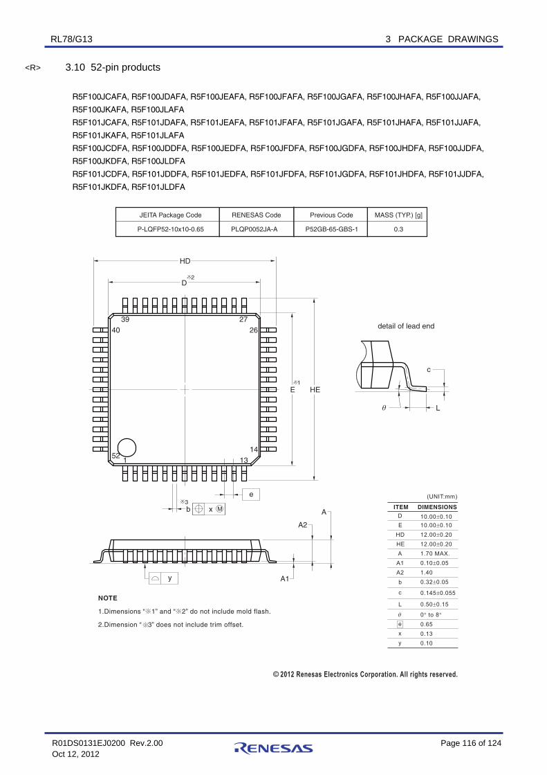
RL78/G13 3 PACKAGE DRAWINGS
Page 116 of 124R01DS0131EJ0200 Rev.2.00 Oct 12, 2012
3.10 52-pin products
R5F100JCAFA, R5F100JDAFA, R5F100JEAFA, R5F100JFAFA, R5F100JGAFA, R5F100JHAFA, R5F100JJAFA,
R5F100JKAFA, R5F100JLAFA
R5F101JCAFA, R5F101JDAFA, R5F101JEAFA, R5F101JFAFA, R5F101JGAFA, R5F101JHAFA, R5F101JJAFA,
R5F101JKAFA, R5F101JLAFA
R5F100JCDFA, R5F100JDDFA, R5F100JEDFA, R5F100JFDFA, R5F100JGDFA, R5F100JHDFA, R5F100JJDFA,
R5F100JKDFA, R5F100JLDFA
R5F101JCDFA, R5F101JDDFA, R5F101JEDFA, R5F101JFDFA, R5F101JGDFA, R5F101JHDFA, R5F101JJDFA,
R5F101JKDFA, R5F101JLDFA
y
e
xb M
L
c
HD
HE
A1
A2
A
D
E
ITEM DIMENSIONS
DE
HDHEA
A1A2 1.40
c
exy
0.650.130.10
L
detail of lead end
b
13
26
152
14
2740
39
2
1
3
0.3P-LQFP52-10x10-0.65
JEITA Package Code RENESAS Code
PLQP0052JA-A
Previous Code
P52GB-65-GBS-1
MASS (TYP.) [g]
NOTE
1.Dimensions “ 1” and “ 2” do not include mold flash.
2.Dimension “ 3” does not include trim offset.
2012 Renesas Electronics Corporation. All rights reserved.
(UNIT:mm)
10.00±0.1010.00±0.1012.00±0.2012.00±0.201.70 MAX.0.10±0.05
0.32±0.05
0.145±0.055
0.50±0.15
0° to 8°
<R>

RL78/G13 3 PACKAGE DRAWINGS
Page 117 of 124R01DS0131EJ0200 Rev.2.00 Oct 12, 2012
3.11 64-pin products
R5F100LCAFA, R5F100LDAFA, R5F100LEAFA, R5F100LFAFA, R5F100LGAFA, R5F100LHAFA, R5F100LJAFA,
R5F100LKAFA, R5F100LLAFA
R5F101LCAFA, R5F101LDAFA, R5F101LEAFA, R5F101LFAFA, R5F101LGAFA, R5F101LHAFA, R5F101LJAFA,
R5F101LKAFA, R5F101LLAFA
R5F100LCDFA, R5F100LDDFA, R5F100LEDFA, R5F100LFDFA, R5F100LGDFA, R5F100LHDFA, R5F100LJDFA,
R5F100LKDFA, R5F100LLDFA
R5F101LCDFA, R5F101LDDFA, R5F101LEDFA, R5F101LFDFA, R5F101LGDFA, R5F101LHDFA, R5F101LJDFA,
R5F101LKDFA, R5F101LLDFA
JEITA Package Code RENESAS Code Previous Code MASS (TYP.) [g]
P-LQFP64-12x12-0.65 PLQP0064JA-A P64GK-65-UET-2 0.51
NOTEEach lead centerline is located within 0.13 mm ofits true position at maximum material condition.
detail of lead end
θ L
c
Lp
HD
HE
ZD
ZE
L1
A1
A2
A
D
E
16
32
164 17
3349
48
Sy
e
Sxb M
A3
S
0.145 +0.055−0.045
(UNIT:mm)
ITEM DIMENSIONS
D
E
HD
HE
A
A1
A2
A3
12.00±0.20
12.00±0.20
14.00±0.20
14.00±0.20
1.60 MAX.
0.10±0.05
1.40±0.05
0.25
c
θ
e
x
y
ZD
ZE
0.65
0.13
0.10
1.125
1.125
L
Lp
L1
0.50
0.60±0.15
1.00±0.20
3°+5°−3°
0.32 +0.08−0.07b
2012 Renesas Electronics Corporation. All rights reserved.

RL78/G13 3 PACKAGE DRAWINGS
Page 118 of 124R01DS0131EJ0200 Rev.2.00 Oct 12, 2012
R5F100LCAFB, R5F100LDAFB, R5F100LEAFB, R5F100LFAFB, R5F100LGAFB, R5F100LHAFB, R5F100LJAFB,
R5F100LKAFB, R5F100LLAFB
R5F101LCAFB, R5F101LDAFB, R5F101LEAFB, R5F101LFAFB, R5F101LGAFB, R5F101LHAFB,
R5F101LJAFB, R5F101LKAFB, R5F101LLAFB
R5F100LCDFB, R5F100LDDFB, R5F100LEDFB, R5F100LFDFB, R5F100LGDFB, R5F100LHDFB, R5F100LJDFB,
R5F100LKDFB, R5F100LLDFB
R5F101LCDFB, R5F101LDDFB, R5F101LEDFB, R5F101LFDFB, R5F101LGDFB, R5F101LHDFB,
R5F101LJDFB, R5F101LKDFB, R5F101LLDFB
JEITA Package Code RENESAS Code Previous Code MASS (TYP.) [g]
P-LFQFP64-10x10-0.50 PLQP0064KF-A P64GB-50-UEU-2 0.35
Sy
e
Sxb M
θ L
c
Lp
HD
HE
ZD
ZE
L1
A1
A2
A
D
E
A3
S
0.145 +0.055−0.045
(UNIT:mm)
ITEM DIMENSIONS
D
E
HD
HE
A
A1
A2
A3
10.00±0.20
10.00±0.20
12.00±0.20
12.00±0.20
1.60 MAX.
0.10±0.05
1.40±0.05
0.25
c
θ
e
x
y
ZD
ZE
0.50
0.08
0.08
1.25
1.25
L
Lp
L1
0.50
0.60±0.15
1.00±0.20
3°+5°−3°
NOTEEach lead centerline is located within 0.08 mm ofits true position at maximum material condition.
detail of lead end
0.22±0.05b
16
32
1
64 17
33
49
48
2012 Renesas Electronics Corporation. All rights reserved.

RL78/G13 3 PACKAGE DRAWINGS
Page 119 of 124R01DS0131EJ0200 Rev.2.00 Oct 12, 2012
R5F100LCABG, R5F100LDABG, R5F100LEABG, R5F100LFABG, R5F100LGABG, R5F100LHABG,
R5F100LJABG
R5F101LCABG, R5F101LDABG, R5F101LEABG, R5F101LFABG, R5F101LGABG, R5F101LHABG,
R5F101LJABG
R5F100LCDBG, R5F100LDDBG, R5F100LEDBG, R5F100LFDBG, R5F100LGDBG, R5F100LHDBG,
R5F100LJDBG
R5F101LCDBG, R5F101LDDBG, R5F101LEDBG, R5F101LFDBG, R5F101LGDBG, R5F101LHDBG,
R5F101LJDBG
JEITA Package Code RENESAS Code Previous Code MASS (TYP.) [g]
P-VFBGA64-4x4-0.40 PVBG0064LA-A P64F1-40-AA2-2 0.03
ITEM DIMENSIONS
D
E
w
A
A1
A2
e
4.00±0.10
4.00±0.10
0.40
0.05
0.08
0.20
0.60
0.60
0.15
0.20±
±
0.05
0.05
0.89±0.10
0.69
0.25
(UNIT:mm)
x
y
y1
ZD
ZE
b
ZDZE
A
INDEX MARK
A2
A1e
Sw A
Sw B
B
A
Sy
Sy1
S
Sxb A BM
8
7
6
5
4
3
2
1
ABCDEFGH
D
E
INDEX MARK
2012 Renesas Electronics Corporation. All rights reserved.

RL78/G13 3 PACKAGE DRAWINGS
Page 120 of 124R01DS0131EJ0200 Rev.2.00 Oct 12, 2012
3.12 80-pin products
R5F100MFAFA, R5F100MGAFA, R5F100MHAFA, R5F100MJAFA, R5F100MKAFA, R5F100MLAFA
R5F101MFAFA, R5F101MGAFA, R5F101MHAFA, R5F101MJAFA, R5F101MKAFA, R5F101MLAFA
R5F100MFDFA, R5F100MGDFA, R5F100MHDFA, R5F100MJDFA, R5F100MKDFA, R5F100MLDFA
R5F101MFDFA, R5F101MGDFA, R5F101MHDFA, R5F101MJDFA, R5F101MKDFA, R5F101MLDFA
RENESAS Code
P-LQFP80-14x14-0.65 PLQP0080JB-E 0.69
DE
HD
HE
A
A2
bp
c
Lp
x
L1
0.13
0.886
14.0014.00
1.40
Min Nom MaxDimension in Millimeters
A1 0.05
1.35
0.26
1.70
0.20
1.45
0.38
13.8013.80
14.2014.20
0.10 0.20
e
0.736 1.036
0° 8°
A3 0.25
0.125
0.32
0.145L 0.80
1.40 1.80
ZD 0.825ZE 0.825
3°
ySy
e
Sxbp M
L
c
Lp
HD
HE
ZD
ZE
L1
A1
A2
A
E
A3
S
detail of lead end
20
40
180 21
41
D
A
B
AB
6160
P80GC-65-UBT -2
Previous Code MASS (TYP.) [g]JEITA Package Code
ReferanceSymbol
17.00 17.20
17.20
17.40
17.00 17.40
1.60
0.65
0.10
2012 Renesas ElectronicsCorporation. All rights reserved.
<R>

RL78/G13 3 PACKAGE DRAWINGS
Page 121 of 124R01DS0131EJ0200 Rev.2.00 Oct 12, 2012
R5F100MFAFB, R5F100MGAFB, R5F100MHAFB, R5F100MJAFB, R5F100MKAFB, R5F100MLAFB
R5F101MFAFB, R5F101MGAFB, R5F101MHAFB, R5F101MJAFB, R5F101MKAFB, R5F101MLAFB
R5F100MFDFB, R5F100MGDFB, R5F100MHDFB, R5F100MJDFB, R5F100MKDFB, R5F100MLDFB
R5F101MFDFB, R5F101MGDFB, R5F101MHDFB, R5F101MJDFB, R5F101MKDFB, R5F101MLDFB
JEITA Package Code RENESAS Code Previous Code MASS (TYP.) [g]
P-LFQFP80-12x12-0.50 PLQP0080KE-A P80GK-50-8EU-2 0.53
Sy
e
Sxb M
θ L
c
Lp
HD
HE
ZD
ZE
L1
A1
A2
A
D
E
A3
S
0.145 +0.055−0.045
(UNIT:mm)
ITEM DIMENSIONS
D
E
HD
HE
A
A1
A2
A3
12.00±0.20
12.00±0.20
14.00±0.20
14.00±0.20
1.60 MAX.
0.10±0.05
1.40±0.05
0.25
c
θ
e
x
y
ZD
ZE
0.50
0.08
0.08
1.25
1.25
L
Lp
L1
0.50
0.60±0.15
1.00±0.20
3°+5°−3°
NOTEEach lead centerline is located within 0.08 mm ofits true position at maximum material condition.
detail of lead end
0.22±0.05b
20
40
1
80 21
41
61
60
2012 Renesas Electronics Corporation. All rights reserved.

RL78/G13 3 PACKAGE DRAWINGS
Page 122 of 124R01DS0131EJ0200 Rev.2.00 Oct 12, 2012
3.13 100-pin products
R5F100PFAFB, R5F100PGAFB, R5F100PHAFB, R5F100PJAFB, R5F100PKAFB, R5F100PLAFB
R5F101PFAFB, R5F101PGAFB, R5F101PHAFB, R5F101PJAFB, R5F101PKAFB, R5F101PLAFB
R5F100PFDFB, R5F100PGDFB, R5F100PHDFB, R5F100PJDFB, R5F100PKDFB, R5F100PLDFB
R5F101PFDFB, R5F101PGDFB, R5F101PHDFB, R5F101PJDFB, R5F101PKDFB, R5F101PLDFB
Sy
e
Sxb M
L
c
Lp
HD
HE
ZD
ZE
L1
A1
A2
A
D
E
A3
S
0.145
(UNIT:mm)
ITEM DIMENSIONS
D
E
HD
HE
A
A1
A2
A3
14.00±0.20
14.00±0.20
16.00±0.20
16.00±0.20
1.60 MAX.
0.10±0.05
1.40±
+
+
0.05
0.25
c
e
x
y
ZD
ZE
0.50
0.08
0.08
1.00
1.00
L
Lp
L1
0.50
0.60±0.15
1.00±0.20
3° 3°5°
detail of lead end
0.22
0.0550.045
b
25
50
1100 26
517576
±0.05
A
B
AB
JEITA Package Code RENESAS Code Previous Code MASS (TYP.) [g]
P-LFQFP100-14x14-0.50 PLQP0100KE-A P100GC-50-GBR-1 0.69
2012 Renesas Electronics Corporation. All rights reserved.

RL78/G13 3 PACKAGE DRAWINGS
Page 123 of 124R01DS0131EJ0200 Rev.2.00 Oct 12, 2012
R5F100PFAFA, R5F100PGAFA, R5F100PHAFA, R5F100PJAFA, R5F100PKAFA, R5F100PLAFA
R5F101PFAFA, R5F101PGAFA, R5F101PHAFA, R5F101PJAFA, R5F101PKAFA, R5F101PLAFA
R5F100PFDFA, R5F100PGDFA, R5F100PHDFA, R5F100PJDFA, R5F100PKDFA, R5F100PLDFA
R5F101PFDFA, R5F101PGDFA, R5F101PHDFA, R5F101PJDFA, R5F101PKDFA, R5F101PLDFA
B
Sy
e
Sxb M
L
c
Lp
HD
HE
ZD
ZE
L1
A1
A2
A
D
E
A3
S
0.145
(UNIT:mm)
ITEM DIMENSIONS
D
E
HD
HE
A
A1
A2
A3
20.00 0.20
14.00 0.20
22.00 0.20
16.00 0.20
1.60 MAX.
0.10 0.05
1.40 0.05
0.070.08
0.0550.045
0.25
c
e
x
y
ZD
ZE
0.65
0.13
0.10
0.575
0.825
L
Lp
L1
0.50
0.60 0.15
53
1.00 0.20
3
detail of lead end
0.32b +
+
+
30
50
1100 31
518180
A
AB
JEITA Package Code RENESAS Code Previous Code MASS (TYP.) [g]
P-LQFP100-14x20-0.65 PLQP0100JC-A P100GF-65-GBN-1 0.92
2012 Renesas Electronics Corporation. All rights reserved.

RL78/G13 3 PACKAGE DRAWINGS
Page 124 of 124R01DS0131EJ0200 Rev.2.00 Oct 12, 2012
3.14 128-pin products
R5F100SHAFB, R5F100SJAFB, R5F100SKAFB, R5F100SLAFB
R5F101SHAFB, R5F101SJAFB, R5F101SKAFB, R5F101SLAFB
R5F100SHDFB, R5F100SJDFB, R5F100SKDFB, R5F100SLDFB
R5F101SHDFB, R5F101SJDFB, R5F101SKDFB, R5F101SLDFB
Sy
e
Sxb M
Lθ
c
Lp
HD
HE
ZD
ZE
L1
A1
A2
A
D
E
A3
S
0.145
(UNIT:mm)
ITEM DIMENSIONS
D
E
HD
HE
A
A1
A2
A3
20.00±0.20
14.00±0.20
22.00±0.20
16.00±0.20
1.60 MAX.
0.10±0.05
1.40±0.05
0.25
c
e
x
y
ZD
ZE
0.50
0.08
0.08
0.75
0.75
L
Lp
L1
0.50
0.60±0.15
1.00±0.20
detail of lead end
b
38
64
1128 39
65102103
0.22
θ 3°+5°−3°
+0.055−0.045
±0.05
A
B
AB
2012 Renesas Electronics Corporation. All rights reserved.
JEITA Package Code RENESAS Code Previous Code MASS (TYP.) [g]
P-LFQFP128-14x20-0.50 PLQP0128KD-A P128GF-50-GBP-1 0.92

C - 1
Revision History RL78/G13 Data Sheet
Description Rev. Date Page Summary
1.00 Feb 29, 2012 - First Edition issued
2.00 Oct 12, 2012 7 Figure 1-1. Part Number, Memory Size, and Package of RL78/G13: Pin count corrected.
25 1.4 Pin Identification: Description of pins INTP0 to INTP11 corrected.
40, 42, 44 1.6 Outline of Functions: Descriptions of Subsystem clock, Low-speed on-chip oscillator, and General-purpose register corrected.
41, 43, 45 1.6 Outline of Functions: Lists of Descriptions changed.
59, 63, 67 Descriptions of Note 8 in a table corrected.
68 (4) Common to RL78/G13 all products: Descriptions of Notes corrected.
69 2.4 AC Characteristics: Symbol of external system clock frequency corrected.
96 to 98 2.6.1 A/D converter characteristics: Notes of overall error corrected.
100 2.6.2 Temperature sensor characteristics: Parameter name corrected.
104 2.8 Flash Memory Programming Characteristics: Incorrect descriptions corrected.
116 3.10 52-pin products: Package drawings of 52-pin products corrected.
120 3.12 80-pin products: Package drawings of 80-pin products corrected.
All trademarks and registered trademarks are the property of their respective owners. SuperFlash is a registered trademark of Silicon Storage Technology, Inc. in several countries including the United States and Japan.
Caution: This product uses SuperFlash® technology licensed from Silicon Storage Technology, Inc.

NOTES FOR CMOS DEVICES
(1) VOLTAGE APPLICATION WAVEFORM AT INPUT PIN: Waveform distortion due to input noise or a
reflected wave may cause malfunction. If the input of the CMOS device stays in the area between VIL (MAX) and VIH (MIN) due to noise, etc., the device may malfunction. Take care to prevent chattering noise from entering the device when the input level is fixed, and also in the transition period when the input level passes through the area between VIL (MAX) and VIH (MIN).
(2) HANDLING OF UNUSED INPUT PINS: Unconnected CMOS device inputs can be cause of malfunction. If an input pin is unconnected, it is possible that an internal input level may be generated due to noise, etc., causing malfunction. CMOS devices behave differently than Bipolar or NMOS devices. Input levels of CMOS devices must be fixed high or low by using pull-up or pull-down circuitry. Each unused pin should be connected to VDD or GND via a resistor if there is a possibility that it will be an output pin. All handling related to unused pins must be judged separately for each device and according to related specifications governing the device.
(3) PRECAUTION AGAINST ESD: A strong electric field, when exposed to a MOS device, can cause destruction of the gate oxide and ultimately degrade the device operation. Steps must be taken to stop generation of static electricity as much as possible, and quickly dissipate it when it has occurred. Environmental control must be adequate. When it is dry, a humidifier should be used. It is recommended to avoid using insulators that easily build up static electricity. Semiconductor devices must be stored and transported in an anti-static container, static shielding bag or conductive material. All test and measurement tools including work benches and floors should be grounded. The operator should be grounded using a wrist strap. Semiconductor devices must not be touched with bare hands. Similar precautions need to be taken for PW boards with mounted semiconductor devices.
(4) STATUS BEFORE INITIALIZATION: Power-on does not necessarily define the initial status of a MOS device. Immediately after the power source is turned ON, devices with reset functions have not yet been initialized. Hence, power-on does not guarantee output pin levels, I/O settings or contents of registers. A device is not initialized until the reset signal is received. A reset operation must be executed immediately after power-on for devices with reset functions.
(5) POWER ON/OFF SEQUENCE: In the case of a device that uses different power supplies for the internal operation and external interface, as a rule, switch on the external power supply after switching on the internal power supply. When switching the power supply off, as a rule, switch off the external power supply and then the internal power supply. Use of the reverse power on/off sequences may result in the application of an overvoltage to the internal elements of the device, causing malfunction and degradation of internal elements due to the passage of an abnormal current. The correct power on/off sequence must be judged separately for each device and according to related specifications governing the device.
(6) INPUT OF SIGNAL DURING POWER OFF STATE : Do not input signals or an I/O pull-up power supply while the device is not powered. The current injection that results from input of such a signal or I/O pull-up power supply may cause malfunction and the abnormal current that passes in the device at this time may cause degradation of internal elements. Input of signals during the power off state must be judged separately for each device and according to related specifications governing the device.

Notice1. Descriptions of circuits, software and other related information in this document are provided only to illustrate the operation of semiconductor products and application examples. You are fully responsible for
the incorporation of these circuits, software, and information in the design of your equipment. Renesas Electronics assumes no responsibility for any losses incurred by you or third parties arising from the
use of these circuits, software, or information.
2. Renesas Electronics has used reasonable care in preparing the information included in this document, but Renesas Electronics does not warrant that such information is error free. Renesas Electronics
assumes no liability whatsoever for any damages incurred by you resulting from errors in or omissions from the information included herein.
3. Renesas Electronics does not assume any liability for infringement of patents, copyrights, or other intellectual property rights of third parties by or arising from the use of Renesas Electronics products or
technical information described in this document. No license, express, implied or otherwise, is granted hereby under any patents, copyrights or other intellectual property rights of Renesas Electronics or
others.
4. You should not alter, modify, copy, or otherwise misappropriate any Renesas Electronics product, whether in whole or in part. Renesas Electronics assumes no responsibility for any losses incurred by you or
third parties arising from such alteration, modification, copy or otherwise misappropriation of Renesas Electronics product.
5. Renesas Electronics products are classified according to the following two quality grades: "Standard" and "High Quality". The recommended applications for each Renesas Electronics product depends on
the product's quality grade, as indicated below.
"Standard": Computers; office equipment; communications equipment; test and measurement equipment; audio and visual equipment; home electronic appliances; machine tools; personal electronic
equipment; and industrial robots etc.
"High Quality": Transportation equipment (automobiles, trains, ships, etc.); traffic control systems; anti-disaster systems; anti-crime systems; and safety equipment etc.
Renesas Electronics products are neither intended nor authorized for use in products or systems that may pose a direct threat to human life or bodily injury (artificial life support devices or systems, surgical
implantations etc.), or may cause serious property damages (nuclear reactor control systems, military equipment etc.). You must check the quality grade of each Renesas Electronics product before using it
in a particular application. You may not use any Renesas Electronics product for any application for which it is not intended. Renesas Electronics shall not be in any way liable for any damages or losses
incurred by you or third parties arising from the use of any Renesas Electronics product for which the product is not intended by Renesas Electronics.
6. You should use the Renesas Electronics products described in this document within the range specified by Renesas Electronics, especially with respect to the maximum rating, operating supply voltage
range, movement power voltage range, heat radiation characteristics, installation and other product characteristics. Renesas Electronics shall have no liability for malfunctions or damages arising out of the
use of Renesas Electronics products beyond such specified ranges.
7. Although Renesas Electronics endeavors to improve the quality and reliability of its products, semiconductor products have specific characteristics such as the occurrence of failure at a certain rate and
malfunctions under certain use conditions. Further, Renesas Electronics products are not subject to radiation resistance design. Please be sure to implement safety measures to guard them against the
possibility of physical injury, and injury or damage caused by fire in the event of the failure of a Renesas Electronics product, such as safety design for hardware and software including but not limited to
redundancy, fire control and malfunction prevention, appropriate treatment for aging degradation or any other appropriate measures. Because the evaluation of microcomputer software alone is very difficult,
please evaluate the safety of the final products or systems manufactured by you.
8. Please contact a Renesas Electronics sales office for details as to environmental matters such as the environmental compatibility of each Renesas Electronics product. Please use Renesas Electronics
products in compliance with all applicable laws and regulations that regulate the inclusion or use of controlled substances, including without limitation, the EU RoHS Directive. Renesas Electronics assumes
no liability for damages or losses occurring as a result of your noncompliance with applicable laws and regulations.
9. Renesas Electronics products and technology may not be used for or incorporated into any products or systems whose manufacture, use, or sale is prohibited under any applicable domestic or foreign laws or
regulations. You should not use Renesas Electronics products or technology described in this document for any purpose relating to military applications or use by the military, including but not limited to the
development of weapons of mass destruction. When exporting the Renesas Electronics products or technology described in this document, you should comply with the applicable export control laws and
regulations and follow the procedures required by such laws and regulations.
10. It is the responsibility of the buyer or distributor of Renesas Electronics products, who distributes, disposes of, or otherwise places the product with a third party, to notify such third party in advance of the
contents and conditions set forth in this document, Renesas Electronics assumes no responsibility for any losses incurred by you or third parties as a result of unauthorized use of Renesas Electronics
products.
11. This document may not be reproduced or duplicated in any form, in whole or in part, without prior written consent of Renesas Electronics.
12. Please contact a Renesas Electronics sales office if you have any questions regarding the information contained in this document or Renesas Electronics products, or if you have any other inquiries.
(Note 1) "Renesas Electronics" as used in this document means Renesas Electronics Corporation and also includes its majority-owned subsidiaries.
(Note 2) "Renesas Electronics product(s)" means any product developed or manufactured by or for Renesas Electronics.
http://www.renesas.comRefer to "http://www.renesas.com/" for the latest and detailed information.
Renesas Electronics America Inc. 2880 Scott Boulevard Santa Clara, CA 95050-2554, U.S.A.Tel: +1-408-588-6000, Fax: +1-408-588-6130Renesas Electronics Canada Limited1101 Nicholson Road, Newmarket, Ontario L3Y 9C3, CanadaTel: +1-905-898-5441, Fax: +1-905-898-3220Renesas Electronics Europe LimitedDukes Meadow, Millboard Road, Bourne End, Buckinghamshire, SL8 5FH, U.KTel: +44-1628-651-700, Fax: +44-1628-651-804Renesas Electronics Europe GmbHArcadiastrasse 10, 40472 Düsseldorf, Germany Tel: +49-211-65030, Fax: +49-211-6503-1327 Renesas Electronics (China) Co., Ltd.7th Floor, Quantum Plaza, No.27 ZhiChunLu Haidian District, Beijing 100083, P.R.China Tel: +86-10-8235-1155, Fax: +86-10-8235-7679Renesas Electronics (Shanghai) Co., Ltd.Unit 204, 205, AZIA Center, No.1233 Lujiazui Ring Rd., Pudong District, Shanghai 200120, China Tel: +86-21-5877-1818, Fax: +86-21-6887-7858 / -7898 Renesas Electronics Hong Kong LimitedUnit 1601-1613, 16/F., Tower 2, Grand Century Place, 193 Prince Edward Road West, Mongkok, Kowloon, Hong KongTel: +852-2886-9318, Fax: +852 2886-9022/9044Renesas Electronics Taiwan Co., Ltd.13F, No. 363, Fu Shing North Road, Taipei, TaiwanTel: +886-2-8175-9600, Fax: +886 2-8175-9670Renesas Electronics Singapore Pte. Ltd. 80 Bendemeer Road, Unit #06-02 Hyflux Innovation Centre Singapore 339949Tel: +65-6213-0200, Fax: +65-6213-0300Renesas Electronics Malaysia Sdn.Bhd.Unit 906, Block B, Menara Amcorp, Amcorp Trade Centre, No. 18, Jln Persiaran Barat, 46050 Petaling Jaya, Selangor Darul Ehsan, MalaysiaTel: +60-3-7955-9390, Fax: +60-3-7955-9510Renesas Electronics Korea Co., Ltd.11F., Samik Lavied' or Bldg., 720-2 Yeoksam-Dong, Kangnam-Ku, Seoul 135-080, KoreaTel: +82-2-558-3737, Fax: +82-2-558-5141
SALES OFFICES
© 2012 Renesas Electronics Corporation. All rights reserved.Colophon 2.2


