Rights / License: Research Collection In Copyright - Non ...49710/eth-49710-02.pdf · therefore are...
155
Research Collection Doctoral Thesis Optical and Mechanical Properties of Static and Tunable Color Coatings Based on Ultrathin Semiconductors Author(s): Schlich, Franziska Felicitas Publication Date: 2016 Permanent Link: https://doi.org/10.3929/ethz-a-010722090 Rights / License: In Copyright - Non-Commercial Use Permitted This page was generated automatically upon download from the ETH Zurich Research Collection . For more information please consult the Terms of use . ETH Library
Transcript of Rights / License: Research Collection In Copyright - Non ...49710/eth-49710-02.pdf · therefore are...
Research Collection
Doctoral Thesis
Optical and Mechanical Properties of Static and Tunable ColorCoatings Based on Ultrathin Semiconductors
Author(s): Schlich, Franziska Felicitas
Publication Date: 2016
Permanent Link: https://doi.org/10.3929/ethz-a-010722090
Rights / License: In Copyright - Non-Commercial Use Permitted
This page was generated automatically upon download from the ETH Zurich Research Collection. For moreinformation please consult the Terms of use.
ETH Library
DISS. ETH NO. 23588
Optical and Mechanical Properties of
Static and Tunable Color Coatings
Based on Ultrathin Semiconductors
A thesis submitted to attain the degree of
DOCTOR OF SCIENCES of ETH ZURICH
(Dr. sc. ETH Zurich)
presented by
FRANZISKA FELICITAS SCHLICH
M.Sc. in Physics, RWTH Aachen University
born on 26.01.1988
citizen of Germany
accepted on the recommendation of:
Prof. Dr. Ralph Spolenak, examinerProf. Dr. Yves Leterrier, co-examinerProf. Dr. Andre Studart, co-examiner
2016


Summary
Color coatings based on ultrathin semiconductors (< 30 nm) on top of reflectivemetals are attractive because of their considerably smaller film thickness comparedto conventional optical coatings based on transparent layers. The large absorptionin the semiconductor and the wavelength-dependent phase-shift at the semicon-ductor interfaces yield an absorption resonance in the reflectance spectrum andthus the color appearance of the coating. The spectral position of this absorptionresonance depends on the thickness of the semiconductor and a change of only afew nanometers results in a completely different color appearance. These coatingstherefore are promising candidates for ultrathin solar cells or as decorative coatingsfor arts and jewelry.
This dissertation shows that the underlying materials are not exclusively limi-ted to metals. Instead, the metal can be replaced by any material if several layersare used such that the effective optical constant of a highly reflective metal ismimicked. As a proof of concept color coatings with metal, semiconductor, andinsulator substrate materials are presented. Deep and narrow absorption resonancesand hence bright colors are obtained for semiconductors and underlying materialswhose absorption coefficients strongly depend on the wavelength.
The latter result is exploited for tunable color coatings as a small change inthe imaginary part of the refractive index changes the shape and spectral positionof the absorption resonance. Thus, by reversibly switching the semiconductorbetween the amorphous and crystalline phase the color of the coating can be tuned.Amorphization of the semiconductor is achieved by a single femtosecond laser pulseof high intensity and crystallization is obtained by several pulses of low intensity.Reversible color switching between blue and gray is presented for the phase-changematerial Ge2Sb2Te5 (GST). An optical contrast as large as 92 % at wavelengthsaround 572 nm is even demonstrated for the conventional semiconductor Si whichdoes not show a large natural optical contrast between its amorphous and crystallinephase. The base color can be tuned by the thickness of the semiconductor, thechoice of substrate material, and the thickness of a transparent capping layer.
Due to the bistable nature of the color coatings they are promising candida-tes for display applications with low power consumption and as they work inreflectance stable color appearance is even achieved in bright sunlight. However, thefunctionality of static and tunable color coatings is based on the ultrathin brittleSi and GST films. A loss of integrity of these thin films might lead to failure of theentire device. Hence, it is of fundamental interest to characterize their cohesive andadhesive strength. In this work, failure of amorphous and crystalline Si and GSTfilms on the commercially available polyimide substrate Kapton® E is studied.
III

In order to crystallize Si at temperatures below the maximum service temperatureof the Kapton® E substrate, the aluminum-induced layer exchange mechanismis exploited. A parametric study reveal that the crystallization temperature canbe reduced by choosing high sputter powers and low argon pressures during thefabrication process.During uniaxial tensile tests of amorphous and crystalline Si and GST films variousmethods are employed to characterize the failure of the thin films. Reflectanceanisotropy spectroscopy (RAS) is introduced as a new tool to evaluate the onsetstrain of fragmentation of thin brittle films. In comparison with other methodsRAS is more sensitive to first cracks in ultrathin GST films.Generally, thinner coatings exhibit better resistance against cracks due to smallerdefect sizes. Moreover, a compressive residual stress of the coating helps to delaythe onset strain of fragmentation while the opposite is the case for a tensile residualstress. The onset strains of fragmentation of Si and GST are similar but Si exhibitsa larger fracture toughness due to the small Young’s modulus of GST. CrystallineSi delaminates at considerably lower strain values compared to GST, which mightbe caused by the aluminum-induced layer exchange mechanism.Static and tunable color coatings based on amorphous Si as well as amorphous andcrystalline GST show a lower resistance against cracks compared to single Si andGST films which might be due to a size effect.
IV

Zusammenfassung
Herkommliche Interferenzschichten bestehen aus transparenten Schichten, derenDicke in der gleichen Grossenordnung wie die Wellenlange von Licht ist.Farbbeschichtungen, die aus sehr dunnen Halbleiterschichten (< 30 nm) auf starkreflektierenden Metallen bestehen, haben den Vorteil, dass sie deutlich wenigerMaterial benotigen. Die starke Absorption des Halbleiters und die wellenlangen-abhangige Phasenverschiebung an den Halbleitergrenzflachen verursachen eineAbsorptionsresonanz im Reflexionsspektrum und dadurch eine Farberscheinung.Die spektrale Position der Absorptionsresonanz hangt von der Dicke des Halbleitersab und eine Dickenanderung von nur ein paar Nanometern fuhrt zu einer volliganderen Farberscheinung. Solche Beschichtungen sind vielversprechend fur dieAnwendung in dunnen Solarzellen oder als dekorative Beschichtungen in derSchmuckindustrie oder der Kunst.
Diese Dissertation zeigt, dass nicht nur Metalle als Substratmaterial verwen-det werden konnen. Stattdessen kann das Metal durch jedes beliebige Materialersetzt werden, wenn mehrere Schichten verwendet werden. Als Nachweis werdenFarbbeschichtungen mit Metallen, Halbleitern und Isolatoren als Substratmaterialprasentiert. Insbesondere werden tiefe und schmale Absorptionsresonanzen erzielt,wenn die Absorptionskoeffizienten des Halbleiters und des Substratmaterials starkwellenlangenabhangig sind.
Das letztere Ergebnis kann fur schaltbare Farbschichten ausgenutzt werden,da eine kleine Anderung des Imaginarteils des Brechungsindex die Form und spek-trale Position der Absorptionsresonanz beeinflusst. Amorphisation beziehungsweiseKristallisation des Halbleiters andert den Brechungsindex und damit die Farber-scheinung. Dadurch lasst sich die Farbe der Beschichtung durch reversibles Schaltenzwischen der kristallinen und der amorphen Struktur des Halbleiters einstellen.Reversibles Schalten zwischen blau und grau wird fur das PhasenwechselmaterialGe2Sb2Te5 (GST) gezeigt. Der herkommliche Halbleiter Si hat im Gegensatz zuGST keinen grossen naturlichen optischen Kontrast zwischen der amorphen undkristallinen Phase. Trotzdem kann ein optischer Kontrast von 92 % bei einerWellenlange von zirka 572 nm erzeugt werden. Die Basisfarbe und der Kontrastwerden durch die Dicke der Halbleiterschicht, durch die Wahl des Substratmaterialsund die Dicke der transparenten Deckschicht eingestellt.
Die Farbschichten sind bistabil und damit vielversprechend fur Bildschirman-wendungen mit geringem Energieverbrauch. Zusatzlich beruht ihre Funktionsweiseauf Reflexion, wodurch die Farberscheinung auch in hellem Sonnenlicht gegebenist. Jedoch basieren sowohl die statischen als auch die einstellbaren Farbschichtenauf den dunnen, sproden Si und GST Schichten. Das Versagen dieser Schichten
V

kann also zum Ausfall eines ganzen Bildschirms fuhren. Daher ist es von hohemInteresse ihre kohasiven und adhasiven Festigkeiten zu bestimmen. In dieser Arbeitwird das Versagen von amorphen und kristallinen Si und GST Schichten auf denhandelsublichen Polyimidsubstraten Kapton® E untersucht.Der durch Aluminium-induzierte Schichtaustausch wird angewendet, um Si beiTemperaturen unterhalb der maximalen Betriebstemperatur von Kapton® E zukristallisieren. Mit Hilfe einer Parameterstudie wird gezeigt, dass Schichten, beidenen wahrend der Herstellung hohe Sputterleistungen und niedrige Argonflussegenutzt werden, niedrige Kristallisationstemperaturen besitzen.Es werden verschiedene Methoden angewendet, um das Versagen der amorphen undkristallinen Si und GST Dunnschichten zu untersuchen. Es wird gezeigt, dass ersteauftretende Risse in GST Schichten mit Reflexionsanisotropie- Spektroskopie (RAS)bestimmt werden konnen. Im Gegensatz zu anderen angewendeten Methoden kannsie sogar fur sehr dunne GST Schichten verwendet werden.Im Allgemeinen weisen dunnere Schichten auf Grund der kleineren Defektgrosseneinen grosseren Widerstand gegenuber Rissbildung auf. Ausserdem hilft eineDruckeigenspannung der Schicht die ersten Risse zu hoheren Dehnungen hin-auszuzogern, ganz im Gegensatz zu einer Zugeigenspannung. Die ersten Rissein GST und Si treten bei ahnlichen Dehnungswerten auf. Da GST aber einenkleineren Elastizitatsmodul besitzt, weist Si eine grossere, kohasive Bruchzahigkeitauf. Kristalline Si Filme delaminieren bei geringeren Dehnungswerten als GSTSchichten. Dies kann durch den Aluminium-induzierten Schichtaustausch her-vorgerufen werden.Statische und einstellbare Farbbeschichtungen mit amorphen Si, sowie amorphenund kristallinen GST Schichten weisen einen geringeren Bruchwiderstand auf alseinzelne Si und GST Schichten, welches durch einen Grosseneffekt erklart werdenkann.
VI

Contents
Contents
Title I
Summary III
Zusammenfassung V
Contents VII
List of symbols and abbreviations XI
1. Introduction 1
1.1. Motivation . . . . . . . . . . . . . . . . . . . . . . . . . . . . . . . . . 1
1.2. Concept of color appearance . . . . . . . . . . . . . . . . . . . . . . . 3
1.2.1. Color description . . . . . . . . . . . . . . . . . . . . . . . . . 3
1.2.2. Light interaction with material . . . . . . . . . . . . . . . . . 5
1.3. Si and Ge2Sb2Te5 properties . . . . . . . . . . . . . . . . . . . . . . . 8
1.4. Concept of thin film failure . . . . . . . . . . . . . . . . . . . . . . . . 10
2. Static color coatings based on ultrathin semiconductors 13
2.1. Introduction . . . . . . . . . . . . . . . . . . . . . . . . . . . . . . . . 13
2.2. Materials and Methods . . . . . . . . . . . . . . . . . . . . . . . . . . 14
2.3. Results . . . . . . . . . . . . . . . . . . . . . . . . . . . . . . . . . . . 15
2.4. Discussion . . . . . . . . . . . . . . . . . . . . . . . . . . . . . . . . . 17
2.5. Conclusion . . . . . . . . . . . . . . . . . . . . . . . . . . . . . . . . . 22
3. Tunable color coatings based on ultrathin Si and Ge2Sb2Te5 23
3.1. Introduction . . . . . . . . . . . . . . . . . . . . . . . . . . . . . . . . 23
3.2. Materials and Methods . . . . . . . . . . . . . . . . . . . . . . . . . . 24
3.3. Results . . . . . . . . . . . . . . . . . . . . . . . . . . . . . . . . . . . 25
3.4. Discussion . . . . . . . . . . . . . . . . . . . . . . . . . . . . . . . . . 27
3.5. Conclusion . . . . . . . . . . . . . . . . . . . . . . . . . . . . . . . . . 32
4. Aluminum-induced crystallization of ultrathin Si films 35
4.1. Introduction . . . . . . . . . . . . . . . . . . . . . . . . . . . . . . . . 35
4.2. Materials and Methods . . . . . . . . . . . . . . . . . . . . . . . . . . 37
4.3. Results . . . . . . . . . . . . . . . . . . . . . . . . . . . . . . . . . . . 39
4.4. Discussion . . . . . . . . . . . . . . . . . . . . . . . . . . . . . . . . . 43
4.5. Conclusion . . . . . . . . . . . . . . . . . . . . . . . . . . . . . . . . . 43
VII

Contents
5. Mechanical properties of amorphous and crystalline Si films 455.1. Introduction . . . . . . . . . . . . . . . . . . . . . . . . . . . . . . . . 455.2. Materials and Methods . . . . . . . . . . . . . . . . . . . . . . . . . . 465.3. Results . . . . . . . . . . . . . . . . . . . . . . . . . . . . . . . . . . . 48
5.3.1. Residual stress . . . . . . . . . . . . . . . . . . . . . . . . . . 485.3.2. Cohesive and adhesive failure of amorphous and poly-Si . . . . 505.3.3. Cohesive and adhesive failure of Si embedded in the insulator
structure . . . . . . . . . . . . . . . . . . . . . . . . . . . . . . 535.4. Discussion . . . . . . . . . . . . . . . . . . . . . . . . . . . . . . . . . 55
5.4.1. Residual stress . . . . . . . . . . . . . . . . . . . . . . . . . . 555.4.2. Onset strain of fragmentation and delamination . . . . . . . . 555.4.3. Stress transfer length . . . . . . . . . . . . . . . . . . . . . . . 595.4.4. Fracture strength . . . . . . . . . . . . . . . . . . . . . . . . . 605.4.5. Fracture toughness . . . . . . . . . . . . . . . . . . . . . . . . 615.4.6. Onset strain of fragmentation and delamination of Si embed-
ded in the insulator structure . . . . . . . . . . . . . . . . . . 645.5. Conclusion . . . . . . . . . . . . . . . . . . . . . . . . . . . . . . . . . 65
6. Cohesive and adhesive failure of amorphous and crystalline Ge2Sb2Te5
films 676.1. Introduction . . . . . . . . . . . . . . . . . . . . . . . . . . . . . . . . 676.2. Materials and Methods . . . . . . . . . . . . . . . . . . . . . . . . . . 696.3. Results . . . . . . . . . . . . . . . . . . . . . . . . . . . . . . . . . . . 70
6.3.1. Phase analysis . . . . . . . . . . . . . . . . . . . . . . . . . . . 706.3.2. Residual stress . . . . . . . . . . . . . . . . . . . . . . . . . . 716.3.3. Cohesive and adhesive properties . . . . . . . . . . . . . . . . 726.3.4. Reflectance anisotropy spectroscopy . . . . . . . . . . . . . . . 76
6.4. Discussion . . . . . . . . . . . . . . . . . . . . . . . . . . . . . . . . . 796.4.1. Residual stress . . . . . . . . . . . . . . . . . . . . . . . . . . 796.4.2. Cohesive and adhesive properties of GST films . . . . . . . . . 796.4.3. Onset strain of fragmentation and delamination of GST films . 82
6.5. Conclusion . . . . . . . . . . . . . . . . . . . . . . . . . . . . . . . . . 88
7. General discussion 917.1. Long-term color stability . . . . . . . . . . . . . . . . . . . . . . . . . 91
7.1.1. Static color coatings . . . . . . . . . . . . . . . . . . . . . . . 917.1.2. Tunable color coatings . . . . . . . . . . . . . . . . . . . . . . 94
7.2. Application of the tunable color coating . . . . . . . . . . . . . . . . 957.2.1. Introduction . . . . . . . . . . . . . . . . . . . . . . . . . . . . 957.2.2. Resolution . . . . . . . . . . . . . . . . . . . . . . . . . . . . . 967.2.3. Power consumption . . . . . . . . . . . . . . . . . . . . . . . . 977.2.4. Switching speed . . . . . . . . . . . . . . . . . . . . . . . . . . 987.2.5. Cycling numbers . . . . . . . . . . . . . . . . . . . . . . . . . 997.2.6. Mechanical properties . . . . . . . . . . . . . . . . . . . . . . 100
7.3. Conclusion . . . . . . . . . . . . . . . . . . . . . . . . . . . . . . . . . 101
8. Conclusion 103
VIII

Contents
A. Appendix 107A.1. Stretch-tunable distributed Bragg reflectors based on elastomers . . . 107A.2. Voltage-induced color change in elastomers . . . . . . . . . . . . . . . 111A.3. Surface roughness of Kapton E . . . . . . . . . . . . . . . . . . . . . 114A.4. RA signal in the elastic strain regime . . . . . . . . . . . . . . . . . . 115
B. Bibliography 117
Declaration 135
Acknowledgment 137
List of Figures 139
IX


List of symbols and abbreviations
List of symbols and abbreviations
1 eV = 1.602 · 10−19 J 1 electronvolte = 1.602 · 10−19 As Electron chargec = 299 458 792 m/s Speed of lighth = 6.626068 · 10−34 m2kg/s Planck’s constantε0 = 8.854 · 10−12 F/s Vacuum permittivity
AFM Atomic force microscopyAg SilverAl AluminumAILE Aluminum-induced layer exchangeAl2O3 Aluminum oxideAr ArgonAu GoldCdTe Cadmium tellurideCB Conduction bandCr Chromiumdc Direct currentDBR Distributed Bragg reflectorE Young’s modulusε Strainf Frequencyfcc Face-centered cubicFe IronG0 Energy release rateGaSb Gallium antimonideGe GermaniumGST Germanium antimony telluride (Ge2Sb2Te5)hcp Hexagonal close-packedHgTe Mercury tellurideInAs Indium arsenideInSb Indium antimonidek Imaginary part of the refractive indexK1C Fracture toughness
XI
List of symbols and abbreviations
L Mean crack distanceλ Light wavelengthMEMS Microelectromechanical systemMIC Metal-induced crystallizationMILC Metal-induced lateral crystallizationn Refractive indexν Poisson’s ratioNA Numerical apertureξ Stress transfer lengthO2 Molecular oxygenPCM Phase-change materialR Resistancerf Radio frequencyRh RhodiumSEM Scanning electron microscopySi Siliconσf Fracture strengthσres Residual stressSiN Silicon nitrideSiO2 Silicon dioxideT TemperatureTEM Transverse ElectromagneticTi TitaniumTiN Titanium nitrideTiO2 Titanium dioxideTi:sapphire Titanium-sapphire (laser)VB Valence bandXRD X-ray diffraction
XII

Introduction
1. Introduction
In this chapter the motivation, structure, and theoretical background of thethesis are introduced. It gives an overview about color coatings based onthin-film interference and describes the relevant theory about uniaxial tensiletests.
1.1. Motivation
Colors are an integral part of this world and have a large effect on our daily life:Signal colors are used to warn of a danger for instance in road traffic. We areattracted by vivid colors in nature such as the colorful wings of butterflies, and thecolor of our food often tells us if it is flavorful.Humans and animals detect color when the receptors in the eyes interact withthe photons of various wavelengths of visible light. Light interferes with matterand the material properties define which portion of the visible light enters oureye. Geometrical optic is one origin of color appearance and is exploited in struc-tural colors where scattering, diffraction, refraction, or interference are involved.Thin-film interference causes one of the simplest structural colors such as thecolor appearance of soap bubbles or thin oil films. Light that is incident on athin film is partially reflected at the two interfaces of the film. These reflectedbeams interfere and, depending on the thickness and the refractive index of thefilm, the spectrum of the reflected light can be strongly modulated. Stacking twoalternating quarter-wave-thickness layers of transparent thin films with differentrefractive indices results in antireflection coatings or distributed Bragg reflectors(DBRs) depending on the sequence of the layer stack. The former is applied toglasses, windows, or in telescopes for instance while the latter is heavily employed inoptical resonators or waveguides. Generally, only transparent films are consideredfor thin-film interference and absorption in the film does not need to be taken intoaccount. The thickness of the films is on the order of the wavelength of the light.Recently, a new concept of color coatings was introduced by Kats et al. [1].They showed that capping a highly reflective metal (Au) with an ultrathin lossydielectric (Ge) causes an absorption resonance in the visible wavelength range,and consequently a color appearance of the coating. This effect was called stronginterference because absorption plays a major role in contrast to common thin-filminterference coatings. The spectral position of the absorption resonance depends onthe thickness of the dielectric. Changing the thickness of the top layer by only a fewnanometers spectrally shifts the absorption resonance by tens of nanometers. Theauthors demonstrated color appearance from yellow, orange, pink, blue to green forGe film thicknesses between 0 nm and 25 nm.
1

Introduction
These coatings are attractive because of the considerable reduction in layerthickness. Numerous applications are conceivable and partly also demonstratedby today: These coatings are excellent candidates for solar cells [2, 3] becausereducing the thickness of the material ensures less purity defects in the films [4].Consequently, the lifetime of the photo-excited charge carriers is sufficient to reachthe electrical junctions. Moreover, the approach of strong interference is promisingfor new types of photodetectors with improved quantum efficiency, for monitoringthe thickness of the deposition of nanometer-sized semiconductors, or for coloringmetals for arts or jewelry.
The aim of this thesis is to lay the materials foundations for static and tunablecolor coatings based on strong interference and to investigate their optical andmechanical properties:
Chapter 1 introduces the theoretical background of color appearance and failureof thin films due to strain.
Chapter 2 describes the development of static color coatings based on stronginterference. Here, it is demonstrated that optical coatings with ultrathin Sicapping layers are not exclusively limited to metals as underlying materials. Weexplain which optical properties of substrate material and dielectric are required toobtain deep and narrow absorption resonances.
Chapter 3 explores that the strong interference effect can be enlarged to tunablecolor coatings by switching the dielectric between the amorphous and crystallinephase. Color switching is demonstrated for the phase-change material Ge2Sb2Te2(GST) and the semiconductor Si.
Our main findings on the aluminum-induced layer exchange (AILE) mechanismto crystallize ultrathin Si films on polyimides substrates are presented in Chapter 4.
The cohesive and adhesive properties of ultrathin amorphous and crystalline Sion polyimide are presented in Chapter 5. Moreover, the mechanical properties ofa static color coating is investigated.
Chapter 6 introduces the onset strain of fragmentation, the fracture strength,and fracture toughness as well as the onset strain of delamination of thin amorphousand crystalline GST films on polyimide substrates. The cohesive properties of thetunable color coating based on GST are determined.
Chapter 7 discusses possible applications of the developed static and opticalcolor coatings and compares their properties to existing display applications.
Finally, the main conclusions are summarized in Chapter 8.
2

Introduction
1.2. Concept of color appearance
1.2.1. Color description
The portion of the electromagnetic spectrum in the wavelength range from 380 nmto 750 nm is called visible light spectrum [5]. This spectrum includes all colors:Violet has the shortest wavelength and red has the longest. Monochromatic light,which is composed of a single wavelength and mixtures of different wavelengths aredetected by the eye as color. Sir Isaac Newton was the first to demonstrate thata natural white light beam consists of a superposition of all different colors. Heexperimented with prisms, and showed that violet light is refracted the most by aprism and red light the least. This can be explained by Snell’s law:
n1sin(φ1) = n2sin(φ2) (1.1)
Here n1 = 1 is the refractive index of air and n2 is the refractive index of theprism. The incident and refracted angles of light are described by φ1 and φ2. Therefractive index is linked to the density of a material and describes the ratio ofthe wave velocity in vacuum, c, and the wave velocity in a medium v. Materialshows chromatic dispersion which means that n depends on the wavelength λ.Consequently, the refractive angles of different wavelengths differ from each otherwhich explains Newton’s observation.
To define colors, a precise standard needs to be defined which was done by theComission internationale de l’eclairage in 1931. This system is called CIE(1931)XYZ and has the advantage of an absolute color definition and it is able to encompassall colors distinguishable by the human eye. Thereby, a triplet representation ofthe colors is used in analogy to the human eye with its three distinct families ofphotosensitive cells. The process of determining colors is described by ASTM E308-06 [6]. Firstly, an observer is defined by the CIE 1931 standard observer whichcorresponds to a field of view subtending a 2 angle of the retina (2 standardobserver). Three dimensionless color matching functions x(λ), y(λ), and z(λ) (seeFigure 1.1 (a)) mimic the three main families of photosensitive cells in the humanretina. As the curves strongly overlap and the blue color dominates, a clear edgereflector type reflectance curve is necessary to produce a red appearance. The CIEstandard illuminant D65 (see Figure 1.1 (b)) is used to mimic sunlight. The followingequations are obtained from [6]. The tristimulus values are calculated with the helpof a reflectance curve R(λ) and the relative spectral power S(λ) (see Figure 1.1 (b))of the 2 standard observer:
X = k
∫λ
R(λ)S(λ)x(λ)dλ,
Y = k
∫λ
R(λ)S(λ)y(λ)dλ,
Z = k
∫λ
R(λ)S(λ)z(λ)dλ.
(1.2)
3

Introduction
400 500 600 7000.0
0.5
1.0
1.5
2.0
spe
ctr
al tr
istim
ulu
s v
alu
es
wavelength (nm)
x y z
400 500 600 7000
20
40
60
80
100
120(a)
standard illuminant D65
rela
tive p
ow
er
(%)
wavelength (nm)
(b)
Figure 1.1.: (a) The color matching functions x(λ), y(λ), and z(λ) of the 19312 standard illuminant. (b) The relative spectral power distribution of the CIEstandard illuminant D65. The illuminant is normalized to a value of 100 % at 560 nm.Data obtained from [6].
The integration is carried out over the visible wavelength range and the normaliza-tion factor k is defined as:
k = 100/
∫λ
S(λ)y(λ)dλ. (1.3)
In all practical calculations, the integrations are approximated by summations:
X = k∑λ
R(λ)S(λ)x(λ)∆λ,
Y = k∑λ
R(λ)S(λ)y(λ)∆λ,
Z = k∑λ
R(λ)S(λ)z(λ)∆λ.
(1.4)
with k = 100/∑λ
S(λ)y(λ)∆λ.
These tristimulus values can be converted to Lab values, which are described witha three-dimensional coordinate system. The a-axis goes from green (< 0) to red(> 0), the b-axis from blue (< 0) to yellow (> 0), and the L-axis is a measurementof brightness (L=0 is black and L=100 is white) as can be seen in Figure 1.2.
L = 116f(Y/Yn)− 16,
a = 500[f(X/Xn)− f(Y/Yn)],
b = 200[f(Y/Yn)− f(Z/Zn)],
(1.5)
with
f(Q) =
Q1/3, if Q > (6/29)3,841108Q+ 4
29, if Q ≤ (6/29)3.
(1.6)
Xn, Yn, and Zn are defined for each illuminant (e.g. D65: Xn=95.047, Yn=100and Zn=108.883) and describe a white reference point. The difference between two
4

Introduction
L=100b=+120
b=-120
a=+120
a=-120
L=0
Figure 1.2.: Illustration of the CIE Lab color space.
colors can be determined by the geometrical distance in the three-dimensional colorspace:
∆E =√
(L2 − L1)2 + (a2 − a1)2 + (b2 − b1)2. (1.7)
Here, E represents the German word ”Empfindung” and means sensation. Humaneyes start to distinguish two colors if the ∆E-value is larger than 1. However, thehuman sensitivity to color differences depends also on the color. In the saturatedyellow region for instance, a color difference of ∆E=3 is sometimes harder to dis-tinguish than a ∆E= 0.5 in midtone neutrals [7].In computer technology the RGB system is more common and can be calculated fromEquation (1.4). RGB values are given in the interval of [0,255] and are obtained asfollows [8]: RG
B
=
0.0324 −0.0154 −0.00499−0.00969 0.0188 0.0004160.000556 −0.00204 0.0106
XYZ
. (1.8)
with R = 255f(R), G = 255f(G), and B = 255f(B) and
f(Q) =
1.055Q1/2.4 − 0.055, if Q > 0.0031308
12.92Q, otherwise.(1.9)
In this work the Lab values of all simulated reflectance curves were determined bythis calculation and usually the obtained color of the sample corresponds to thecolor of the graph.
1.2.2. Light interaction with material
The origin of colors in nature are described by Nassau [9]. He lists 15 differ-ent mechanisms, which include besides geometrical optics, also excitations andtransitions between energy bands or molecular orbitals and transitions involvingligand-field effects. Here, we focus on two of them, namely the reflectance of metalsand thin-film interference.
5

Introduction
Reflectance of metalsIn contrast to semiconductors or insulators, metals exhibit a shiny appearance.The interaction of light with metals can be explained by electron band theory. Thebonding of two atoms leads to two molecular orbitals, those of four atoms results infour molecular orbitals. Extrapolating this approach for a metal yields to countlessenergy levels which therefore, can be assumed to be continuous. The shape of theseenergy bands depends not only on the atomic orbitals but also on the spacing ofthe atoms. The valence bands include all electrons which are available for bonding.The highest filled electron energy level is called Fermi energy. In metals the valencebands are only partially filled up. There are three relevant optical excitations in ametal [10]:(i) Intraband transition: These transitions involve the excitation of an electron fromaround the Fermi energy to an empty state within the same band. The absorbedlight induces an alternating current on the metal surface which immediately re-emitsthe light out of the metal. Thus, if the absorption and re-emission of the light isequal for all wavelengths in the visible spectrum the metal appears silvery-white.(ii) Interband transition: Excitation of an electron from a valence band close to theFermi level to a conduction band above the Fermi energy requires light energieswhich at least correspond to the energy difference of the two involved bands. Lightthat excites the electrons is absorbed and thus missing in the reflectance spectrum.The onset of interband transitions is easily recognized in the reflectance spectrumof the metal. Gold for instance absorbs photons below 550 nm wavelength andtherefore, blue and green light is missing in the reflectance spectrum which givesgold the typical yellow color appearance.(iii) Plasma frequencies: A metal becomes transparent if the frequency of incominglight exceeds the plasma frequency of the metal. The high density of electrons in ametal leads to a collective oscillation of electrons (plasma) at the plasma frequencydue to the Coulomb interaction. This motion produces fluctuations in the electrondensity. For most metals the plasma frequency lies in the ultraviolet spectral region.
In semiconductors and insulators the Fermi energy lies within a band gap. Theband gap of a semiconductor is small enough to excite an electron from a valenceband to a conduction band with incident light. Consequently, that light is absorbedand the surface of the semiconductor appears dark. The band gap of an insulatoris too large to excite any electrons from the valence band to the conduction band.Hence, light passes through a perfect insulator and it appears transparent. Someinsulators have defects such as pores where the light is scattered and the insulatorappears white.
Thin-film interferenceReflected and transmitted light from thin-film interference can be calculated fromthe so-called transfer matrix method. The analysis is carried out in terms of thequantities defined in Figure 1.3 and in analogy to [11, 12]. The boundary conditionsstate that the tangential components of the electric field E and the magnetic fieldB are continuous across the interfaces I and II (see Figure 1.3). Consequently, theirmagnitudes on either sides are equal. The electric field E is chosen perpendicularto the normal vector of the plane of incidence.
6

Introduction
Table 1.1.: Boundary conditions
First interface
Electric E0 + Er1 = Et1 + Ei1
MagneticB0cos(θ0)−Br1cos(θ0) = Bt1cos(θi1)−Bi1cos(θi1)
n0E0cos(θ0)− n0Er1cos(θ0) = n1Et1cos(θi1)− n1Ei1cos(θi1)Second interface
Electric Et1exp(−iδ) + Ei1exp(iδ) = Et2
MagneticBt1cos(θi1)exp(−iδ)−Bi1cos(θi1)exp(iδ) = Bt2cos(θt2)
n1Et1cos(θi1)exp(−iδ)− n1Ei1cos(θi1)exp(iδ) = nsEt2cos(θt2)
The phase factors exp(iδ) and exp(−iδ) with the phase difference δ =(2π/λ)n1d cos(θi1) at the second interface result from the fact that the light trav-els through the film with thickness d. Moreover, it is taken into account that themagnitude of the electric field is the product of the wave speed (v = c/n) times themagnitude of the magnetic field. In the following, Ei1 and Et1 are eliminated fromthe equations in Table 1.1:
1 +Er1E0
=Et2E0
[cos(δ)− γs
γ1i sin(δ)
], (1.10)
γ0 − γ0Er1E0
=Et2E0
[−iγ1 sin(δ) + γs cos(δ)] , (1.11)
with γ0 ≡ n0 cos(θ0), γ1 ≡ n1 cos(θi1), and γs ≡ ns cos(θt2). Equation (1.10) and
d
θ0
θt2
θi1
EB n0
n1
ns
E0
Et1
Ei2 Er2
Et2
Ei1
Er1I
II
film
substrate
Figure 1.3.: Illustration of thin-film interference. The labeling corresponds to thederivation of the transfer matrix method in the text. The figure was motivated by[11].
7

Introduction
(1.11) written in matrix form yields:[1γ0
]+
[1−γ0
]Er1E0
=
[cos(δ) − i sin(δ)
γ1
−iγ1 sin(δ) cos(δ)
] [1γs
]Et2E0
, (1.12)
which can be written as: [1γ0
]+
[1−γ0
]r = M
[1γs
]t. (1.13)
M is known as transfer matrix, r is the reflection coefficient, and t the transmissioncoefficient. Equation (1.13) can be generalized for N layers with refractive indicesn1, n2, n3,..., nN : [
1γ0
]+
[1−γ0
]r = M1M2M3...MN
[1γs
]t, (1.14)
where the transfer matrices of the various layers are denoted with M1, M2, M3,...,MN . If the elements of the overall transfer matrix M are A, B, C, and D,
M =
[A BC D
], (1.15)
Equation (1.13) can be solved for r and t as follows:
r =γ0A+ γsγ0B − C − γsDγ0A+ γsγ0B + C + γsD
, (1.16)
t =2γ0
γ0A+ γsγ0B + C + γsD. (1.17)
The reflectance R and the transmittance T are given by R = |r|2 and T = |t|2.
1.3. Si and Ge2Sb2Te5 properties
This work focuses on the semiconductors Si and Ge2Sb2Te5 (GST) applied tooptical coatings based on strong interference. Hence, the most important propertiesand applications of Si and GST are shortly introduced.Si:The semiconductor Si is one of the most abundant materials on earth and canbe found as compound in nature such as oxide or nitride. Elemental silicon isfabricated by reducing silica (SiO2) in a high temperature furnace with coke asreducing agent [13]. Besides wafer applications, silicon is heavily employed inelectronics and solar cells. It has a diamond crystalline structure which consists oftwo interpenetrated face-centered cubic (fcc) lattices overlapped with an offset of anunit cell vector of (1/4, 1/4, 1/4). Silicon is a semiconductor with an indirect bandgap in which the valence band (VB) maximum is at another wave vector in k-spacethen the conduction band (CB) minimum. Therefore, recombination of an electronin the VB with a hole in the CB requires an interaction with a phonon to conservemomentum. This phonon interaction leads to heating of the crystal. The intrinsic
8

Introduction
Table 1.2.: Crystal structure, band gap, and crystallization temperature TC of Siand Ge2Sb2Te5.
Si Ge2Sb2Te5
amorphous metastable stablecrystal structure diamond fcc hexagonalband gap 1.12 eV [15] 0.7 eV [16] 0.5 eV [16] 0.5 eV [16]TC ≈800 C [17] ≈170 C [18] ≈270 C [18]
crystallization temperature of silicon is relatively high (see Table 1.2) and can bereduced by the presence of a metal: (i) The formation of compounds (silicide) helpsto decrease the crystallization temperature. This is the case for Si in contact with ametal such as Ni, Pd, or Cu. (ii) Metals such as Al, Au, or Ag result in an eutecticmetal-silicon system. Here, the silicon bonds are weakened and silicon nucleationis promoted [14]. This metal-induced crystallization is a promising approach forfabricating polycrystalline Si (poly-Si) films on cheap substrates such as glass orplastic and is employed in this work to investigate the mechanical properties ofpoly-Si on polyimide substrates (see Chapter 4 and 5).
Ge2Sb2Te5:Ge2Sb2Te5 (GST) belongs to the rare class of phase-change materials (PCMs). Theycan be rapidly and reversibly cycled between the amorphous and crystalline state.The reflectivity contrast between the two phases is up to 30 % [20] and is exploitedin rewritable optical data storage. The electrical resistivity changes up to several
time
temperature
melting
crystallization
ambient
Figure 1.4.: Illustration of a thermal cycle. The amorphous phase-change materialis crystallized by a heating pulse above the crystallization temperature. Reamor-phization occurs by melting the phase-change material and subsequently, rapid cool-ing of the liquid phase. This figure was motivated by [19].
9
Introduction
orders of magnitude upon the phase transition [21] and offers great potential asnon-volatile electronic memory. The principle of a thermal cycle is demonstratedin Figure 1.4. Crystallization of the PCM is realized by a low intensity heatingpulse either by a laser pulse in optical data storage application or by an electricalcurrent pulse in electronic memory devices. Heating the material above the glasstransition temperature enables the atoms to arrange in the energetically favorableperiodic structure. The crystallization time is the limiting factor for the switch-ing speed [22]. Amorphous GST crystallizes in the meta-stable face-centered cubicNaCl structure where the Ge and Sb atoms and the vacancies randomly distributethe ”Na” sites (4(b)) and the Te atoms are located at the ”Cl” sites (4(a)) [23].However, Kolobov et al. suggest a displacement of the Sb and Ge atoms such thatthe Ge atoms switch from tetrahedral to octahedral positions upon phase-change[24]. For GST the crystallization is nucleation-dominated in contrast to the PCMAgInSbTe which is growth-dominated [25]. The crystallization temperature andtime strongly depends on the GST film thickness but also on the capping layer [26].Reamorphization of the crystalline bit is obtained by a short laser or current pulseof high intensity to melt the material. A cooling rate higher than 109 K/s quenchesthe melt into the amorphous phase [22].Although, the first phase-changing electrical characteristic was already discoveredin 1917 by Waterman and since then numberless researchers have investigated andimproved the properties of phase-change materials, still some open questions andchallenges remain. For instance the large thickness decrease (GST: 6.5 % [27]) uponcrystallization yields to void formation over the bottom electrode [28]. Hence, thedevice can no longer be switched to the low resistance state and the cycling numberis reduced.Comparing the properties of GST to those of Si raises the question why a semi-conductor such as Si is unfavorable as phase-change material. The atoms in crys-talline Si form tight covalent bonds with each surrounding atom which yields a highmelting temperature. Hence, a large energy needs to be applied to amorphize Si.Moreover, the high viscosity of amorphous Si results in slow atomic diffusion andtherefore long crystallization times.
1.4. Concept of thin film failure
Stress in a thin film has three main origins which might lead to failure of the thinfilm: Thermal, intrinsic, and mechanical [29]. Thermal and intrinsic stress are sum-marized as residual stress and result from fabrication processes. For instance, duringsputter deposition different parameters such as grain growth, phase transitions, orion bombardment of the film may generate stress in the film. Moreover, differencesin thermal expansion coefficients of film and substrate yield stress due to tempera-ture changes. Here, the focus is on mechanical stress which arises from mechanicalloads.The tensile stress in a thin film on a compliant substrate increases during uniaxialloading. As soon as the stress exceeds the fracture strength of the largest defect, acrack is formed and grows perpendicular to the loading direction. The strain valueat which the first crack occurs is called onset strain of fragmentation εon and de-
10

Introduction
0.01 0.1
1
10
100
1000
εsat
εc
mea
n c
rack
dis
tan
ce L
(µm
)
strain ε
εon
Lsat
Lc
Figure 1.5.: Example of mean crack distance as a function of strain. The first crackin the film appears at the onset strain of fragmentation εon. At the transition fromthe first to the second regime at εc the stress relaxation zones start to overlap. In thethird regime at εsat no more cracks occur and the mean crack distance Lsat saturates.
pends on the film thickness and the material properties. Generally, the onset strainof fragmentation decreases with increasing film thickness because there are fewerdefects in smaller film volumes. Hence, the probability of a critical defect at anapplied strain is smaller for thinner films. The tensile stress in the film is releasedclose to the crack in the so-called stress relaxation zone. More cracks appear as soonas the stress in the film reaches the failure stress of further defects. The distancebetween the cracks decreases rapidly with increasing strain in this defect-controlledregime [30]. In the second regime, the fragmentation density is so high that stressrelaxation zones start to overlap and further cracks occur mainly in the center offragments at maximized stress. At large strains no or only few additional cracksappear because of substrate yielding. Figure 1.5 presents the mean crack distanceas a function of strain for the three regimes.The lateral contraction mismatch of substrate and coating leads to the formation
of compressive stress in the coating perpendicular to the loading direction. Duringstraining this compressive stress increases and induces delamination of the coating.Generally, delamination of the film start at the fragmentation boundaries at thelocation of maximal compressive stress.
11


Static color coatings based on ultrathin semiconductors
2. Static color coatings based onultrathin semiconductors
This chapter presents that optical coatings based on ultrathin highly absorb-ing dielectrics are not limited exclusively to metals as underlying materialas assumed previously. We demonstrate that the underlying metal can bereplaced by any material if several layers are used such that the effectiveoptical constant resembles that of a highly reflective metal. Consequently,the optical properties are tunable by the choice of material, the number oflayers, and the layer thickness and are hence more adaptable to the potentialapplication.The main findings presented in this chapter are published in Applied PhysicsLetters [31].
2.1. Introduction
Light interacting with nano- or microstructures results in intense and bright colorsbecause of diffraction, scattering, or thin-film interference [9]. For instance, therehave been numerous demonstrations of colors caused by interference in periodic mul-tilayers [32–35]. The optical thicknesses of those transparent films are usually onthe order of the wavelength [11]. Recently, Kats et al. [1] presented a new techniquebased on thin-film interference in ultrathin (5 - 25 nm) highly absorbing dielectricson metals. The considerable reduction of the film thickness in comparison to trans-parent layers is enabled by a combination of the large absorption in the dielectricand the non-trivial phase-shift at the interface between metal and dielectric. A non-trivial phase-shift is not only limited to 0 or π as for transparent materials or perfectelectric conductors but is wavelength-dependent. The resulting strong absorptionresonance depends on the thickness such that various but not all bright colors aretunable.In this work we show that thin-film interference in ultrathin dielectrics does notonly appear on metals, but also on insulator layers and semiconductor structures.The required non-trivial phase-shift at the interface between the dielectric and theunderlying material, as well as the high reflectance of the latter, are tunable by thenumber and thickness of the layers. In our devices, only one (two) bilayer(s) ofinsulators (semiconductors) are necessary for color appearance because of the lowreflectance of the Si substrate. In contrast, it has been simulated [2] that anti-reflection resonances based on ultrathin dielectrics in solar cells require four to sixbilayers. For color coatings based on ultrathin dielectrics, metals can be replaced bystacks of layers of various materials, provided their effective optical constants resem-ble those of a highly reflective metal. The effective optical constant is the optical
13

Static color coatings based on ultrathin semiconductors
constant of an equivalent semi-infinite medium which can replace the multilayersand has the same optical properties.
2.2. Materials and Methods
Schematics of the three different studied structures are presented in Figure 2.1. Theinsulator and semiconductor structure were designed with the help of simulations.In a first step quarter-wave-thickness layers (at λ= 550 nm) with the high index ma-terial on top of the low index material were chosen as starting parameters to increasethe reflectance of the multilayers (in analogy to a distributed Bragg reflector). In asecond step the thickness of the layers were optimized for bright color appearance.We used amorphous Si with thicknesses between 0 and 30 nm as dielectric. Forthe metal structure 86 nm thick Au was utilized. The insulator structure comprisesamorphous SiO2 and amorphous TiO2 while the semiconductor structure consistsof a double layer of amorphous Ge and amorphous Si. All films were prepared bysputter deposition.The Au and TiO2 films were deposited by direct current (dc) and the Si, SiO2, andGe films by alternating current (ac) sputter deposition on (100) oriented Si wafers.The substrate was rotated during deposition in order to achieve uniform film thick-nesses and the base pressure in the sputter chamber was lower than 10−4 Pa. Foreach structure the layers were deposited on the polished (smooth) surface and onthe unpolished (rough) surface of a Si wafer to specify the sensitivity of the color tothe angle of incidence of the light. The reflectances of the different structures weredetermined with a fiber spectrometer. The measurements were performed at anincidence angle of 0 and at wavelengths ranging from 300 to 800 nm. The refractiveindices of SiO2 and TiO2 were measured by ellipsometry at an incidence angle of70 and the ellipsometric parameters Ψ and ∆ were fitted with the Cauchy equation[36]. The refractive indices of Au [37], amorphous and crystalline Si [38], and amor-phous [39] and crystalline [40] Ge were obtained from literature. The reflectance fors-polarized light was simulated with the transfer matrix method which can be foundin optics textbooks [11, 41]. The colors of the samples were calculated from the sim-ulated reflectance curves in analogy to [6] by using the standard illuminant D65 [42]
semiconductor structure
(c)
insulator structure
(b)
metal structure
86 nm Au
Si
32 nm Si29 nm GeSi
76 nm TiO2
85 nm SiO2
Si
(a)
32 nm Si29 nm Ge
Figure 2.1.: Schematics of the different samples comprising ultrathin Si with thick-nesses between 0 and 30 nm are presented. The underlying materials are (a) Au(metal structure), (b) TiO2 and SiO2 (insulator structure), and (c) a double layerof Ge and Si (semiconductor structure).
14

Static color coatings based on ultrathin semiconductors
and the color matching functions [42] of the 1931 2 standard observer as describedin Chapter 1. A Raman measurement was performed with a green laser (532.24 nm)and at low laser power of 0.5 mW to avoid a crystallization of the semiconductors[43].
2.3. Results
Figure 2.2 shows photographs of the various sample structures with variable Si thick-nesses deposited as top layer. The photographs demonstrate bright color appear-ance for the metal and insulator structures. The colors of the metal structure on thesmooth surface are in good agreement with those on the rough surface. However,this is not the case for the two other structures which indicates that the reflectancesof the insulator and semiconductor structure vary more strongly with the angle ofincidence of the light as compared to the metal structure. To support these find-ings theoretically, the incident angle-dependent reflectance was simulated for eachstructure coated with 15 nm Si (see Figure 2.3).
smooth surface
rough surface
I II III
IV V VI
VII VIII IX
II V
VI VII
I III IIIII III
IVIV V VVI VI
VIIVII VIII VIIIIX IX
II II
VI VIVII VII
III III
metal structure insulator structure
semiconductor structure
Figure 2.2.: I-IX: 0, 3, 5, 7, 10, 15, 20, 25, and 30 nm of Si deposited on the differentsample structures on the polished side (smooth surface) and on the unpolished side(rough surface) of a Si wafer. The metal and insulator structures create a spectrumof bright colors from yellow, red, pink to blue while the semiconductor structurechanges from gray to blue.
The absorption resonance of the metal structure remains prominent for angles ofincidence from 0 to approximately 80. However, the reflectance of the insulatorstructure is constant between 0 and 60 and the semiconductor structure onlybetween 0 and 30. Consequently, especially the reflectance of the semiconductorstructure is strongly dependent on the angle of incidence of the light.
Figure 2.4 presents the experimental and calculated reflectance spectra of themetal, insulator, and semiconductor structures. The reflectance spectra were mea-sured and calculated for the structures without Si and with Si in the thickness rangebetween 5 nm and 30 nm. The colors of the graphs correspond to the measured or
15

Static color coatings based on ultrathin semiconductors
incid
ent angle
(°)
wavelength (nm)
(a)
400 600 8000
20
40
60
80
wavelength (nm)
(b)
400 600 800wavelength (nm)
(c)
400 600 8000
50
100
refle
cta
nce
(%
)
Figure 2.3.: Simulated reflectance spectra with s-polarized light for a 15 nm Si layeron (a) the metal structure, (b) the insulator structure, and (c) the semiconductorstructure. The optical properties of the metal structure are more robust with respectto the incident angle than those of the two other structures. Nevertheless, thereflectances of all structures remain at least prominent between 0 and 30.
simulated colors of the sample. While the simulated and measured reflectance spec-tra and sample colors given in Figure 2.4 (a)-(f) are in excellent agreement with eachother, small deviations between measurements and simulations can be explainedby differences between the refractive indices of the sputtered films and those takenfrom literature caused by, e.g., different densities [44]. Both, the reflectance of themetal and the insulator structure show distinct absorption resonances which shiftto longer wavelengths with increasing Si thickness. These distinct absorption reso-nances result in bright colors including yellow, orange, red, purple, and blue. Alsothe reflectance spectra of the semiconductor structure exhibit absorption resonances.However, they are not as deep and narrow as those of the other two structures. Con-sequently, the color appearance only changes from gray to blue as a function of Sifilm thickness.
16

Static color coatings based on ultrathin semiconductors
300 400 500 600 700 8000
20
40
60
80
100
(f)
(d)
(b)
semiconductor structuresemiconductor structure
insulator structureinsulator structure
metal structure
refle
cta
nce
(%
)re
flecta
nce
(%
)re
flecta
nce
(%
)
Si: 0 nm 5 nm 10 nm 15 nm 20 nm 25 nm 30 nm
reflecta
nce (
%)
wavelength (nm)
metal structure
300 400 500 600 700 8000
20
40
60
80
100
Si: 0 nm 5 nm 10 nm 15 nm 20 nm 25 nm 30 nm
wavelength (nm)
300 400 500 600 700 8000
20
40
60
80
100
Si: 0 nm 5 nm 10 nm 15 nm 20 nm 25 nm 30 nm
refle
cta
nce
(%
)
wavelength (nm)
300 400 500 600 700 8000
20
40
60
80
100
Si: 0 nm 5 nm 10 nm 15 nm 20 nm 25 nm 30 nm
wavelength (nm)
300 400 500 600 700 8000
20
40
60
80
100
Si:
0 nm 5 nm 10 nm 15 nm 20 nm 25 nm 30 nm
refle
cta
nce
(%
)
wavelength (nm)
300 400 500 600 700 8000
20
40
60
80
100(e)
(c)
simulationmeasurement
Si:
0 nm 5 nm 10 nm 15 nm 20 nm 25 nm 30 nm
wavelength (nm)
(a)
Figure 2.4.: Measured (a), (c), (e) and simulated (b), (d), (f) reflectance spectra ofthe different sample structures covered with 0 to 30 nm thick Si layers. The colors ofthe graphs correspond to the measured and simulated colors of the samples. Mea-surement and simulation are in good agreement. While deep absorption resonancesand consequently bright colors are obtained for the metal and insulator structure,this is not the case for the semiconductor structure.
2.4. Discussion
The weak absorption resonances and hence also slightly pronounced colors of thesemiconductor structure indicate that bright colors of the samples are obtained onthe following three conditions:
• Non-trivial phase-shift: As already stated by Kats et al. [1], a non-trivialphase-shift at the interface between the dielectric and the underlying structureis required for an absorption resonance. This is fulfilled by using metal orsemiconductor materials or several layers of insulator material as substrate.
• Minimal reflectance: A minimal reflectance of the underlying material guar-antees the possibility of a deep absorption resonance and consequently a bright
17

Static color coatings based on ultrathin semiconductors
0
20
40
60
80
100 InAs: 0 nm 5 nm 10 nm 15 nm 20 nm 25 nm
(b) (c)
re
flecta
nce (
%)
300 400 500 600 700 8000
1
2
3
4
5
n Fe k Fe n InAs k InAs
InAs on Fe
refr
activ
e in
dex
wavelength (nm)
300 400 500 600 700 8000
1
2
3
4
5
n Au k Au n HgTe k HgTe
refr
activ
e in
dex
wavelength (nm)
(a)
0
20
40
60
80
100 HgTe: 0 nm 5 nm 10 nm 15 nm 20 nm 25 nm
refle
cta
nce (
%)
0
20
40
60
80
100 InAs: 0 nm 5 nm 10 nm 15 nm 20 nm 25 nm
refle
cta
nce (
%)
300 400 500 600 700 8000
1
2
3
4
5
HgTe on Au
n Au k Au n InAs k InAs
refr
activ
e in
dex
wavelength (nm)
InAs on Au
Figure 2.5.: Simulated reflectance spectra and colors with the corresponding refrac-tive indices of different semiconductors on Au and Fe. The refractive indices of InAs,HgTe, and Fe were taken from literature [37–39]. The positions of the absorptionresonances are highlighted in gray. Narrow absorption resonances are observed if|dk/dλ| of the metal and the dielectric are large. While in (a) only |dk/dλ| of thedielectric is large, in (b) only the absorption of the metal is strongly dependent onthe wavelength at wavelengths between 520 and 580 nm. In (c) an ideal combinationof metal and dielectric is presented: |dk/dλ| of both materials is pronounced in thesame wavelength range and consequently bright colors are obtained.
color. The required reflectance of above 60 % is given for most metals and istunable by several layers for all other materials.
• Dispersion: Narrow absorption resonances occur at wavelengths λ where|dk/dλ| of the underlying material and the dielectric are large (in the follow-ing dispersion). Here, k is the imaginary part of the refractive index. Thegray highlighting in Figure 2.5 indicates that absorption resonances indeed ap-pear as well when only |dk/dλ| of the dielectric is large (see Figure 2.5 (a)).However, bright colors and distinct absorption resonances are only obtainedif the absorption of both materials are strongly varying with the wavelengthas presented in Figure 2.5 (c). Figure 2.5 (b) shows that a large |dk/dλ| of themetal is not sufficient for an absorption resonance (see particularly in the wave-length range between 520 nm and 580 nm). In the following, the dependence ofthe absorption resonance on the material dispersion is derived in a simulation.Therefore, the reflection coefficient is calculated with light incident at an angleof 0 [41]:
r =r12 + r23e
2iβ
1 + r12r23e2iβ, (2.1)
with the Fresnel formulae rmn = (nm − nn)/(nm + nn) and β = (2π/λ)n2h2.Here, n is the complex refractive index n = n+ ik, h the film thickness, and λis the wavelength. Layer 1 is air, layer 2 is the semiconductor and layer 3 themetal. An absorption resonance (r ≈ 0) only occurs for some combinationsof the refractive indices of both materials. A large |dk/dλ| causes stronglywavelength-dependent refractive indices. Therefore, the ideal combinations of
18

Static color coatings based on ultrathin semiconductors
the refractive indices for r ≈ 0 are given at a small (large) wavelength rangeif |dk/dλ| is large (small). Consequently, large |dk/dλ| lead to narrow absorp-tion resonances and bright colors. To demonstrate this, the reflectance of ah2=15 nm thin InAs film on Au is simulated for different |dk/dλ|. Therefore,all parameters in Equation 2.1 are kept constant and only k(λ) is approximatedlinearly in small intervals of λ− λ0=1 nm. |dk/dλ| can then be tuned locallywith the help of the factor m:
k(λ) = k(λ0) +mdk(λ0)
dλ(λ− λ0). (2.2)
Figure 2.6 presents the simulated reflectances for three different |dk/dλ|. If|dk/dλ| of both materials is increased (m=1.3) the width of the absorption res-onance is focused to a smaller wavelength range than for the original |dk/dλ|(m=1) and consequently, a brighter color is expected. A smaller |dk/dλ|(m=0.7) leads to a broader absorption resonance. Consequently, absorptionresonances in materials with large |dk/dλ| are expected to generate bright col-ors. However, it could be argued that not |dk/dλ| but the different value of korigins the change of the shape of the absorption resonance. This can be ruledout, since an offset of k has the same effect as a different thickness of the semi-conductor structure (optical path d = h ·n). Another approach to understandthe dispersion dependence of the absorption resonance is in analogy to thework by Zhang et al. [2]. They tried to expand the phase of r23(φ(r23)) in thewavelength range from 550 nm to 650 nm to achieve anti-reflection resonancein this range with ultrathin semiconductors. As the following conditions areusually fulfilled, a large |dk/dλ| of both materials causes an increasing dif-ference between k2 and k3 with respect to the wavelength. Above the bandgap energy |dk/dλ| of a semiconductor is mostly negative. The absorptionof a semiconductor decreases with increasing wavelength (decreasing energies)because the energy of the photons must be larger than the band gap. Formetals, |dk/dλ| is larger or equal to zero. In the latter case, the efficiency ofabsorption and re-emission of light is equal at all optical energies and |dk/dλ|is greater than zero if the efficiency depends on selection rules.
φ(r23) = tan−1
(Im(r23)
Re(r23)
)(2.3)
φ(r23) = tan−1
(2n2(k3 − k2) + 2k2(n2 − n3)
(k3 − k2)2 + 2k2(k3 − k2) + n23 − n2
2
). (2.4)
Consequently, a large |dk/dλ| of both materials (i.e. k3 − k2 is stronglywavelength-dependent) leads to a larger expansion of the phase (see Equa-tion 2.4) and has the same effect as tuning the phase. However, our approachhas the advantage that the refractive indices of the materials are in most casesgiven in literature and therefore, it is not necessary to calculate the phase.In summary, a large |dk/dλ| leads to narrow absorption resonances since theideal refractive indices for a reflectivity r ≈ 0 are limited to small wavelengthranges. This condition is in agreement with the observation of [1], where
19

Static color coatings based on ultrathin semiconductors
(a) (b) (b)
400 600 8000
1
2
3
k In
As
wavelength (nm)
400 600 8000
2
4
6
k Au
wavelength (nm)
400 600 8000
20
40
60
80
100
refle
ctan
ce (
%)
wavelength (nm)
m=0.7 m=1.0 m=1.3
Figure 2.6.: The imaginary part of the refractive index of InAs (a) and Au (b) isshown. A change of the slope m of the refractive indices of InAs and Au causes achange of the absorption resonance (c). An increase of |dk/dλ| (m=1.3) leads toa sharper reflectance minimum and consequently, a brighter color is expected. If|dk/dλ| is decreased (m=0.7) the absorption resonance is expanded.
bright colors for ultrathin Ge films on Au (large |dk/dλ| of Ge and Au) andonly pastel colors for Ge on Ag were obtained. Remarkably, bright colors canbe observed for thin amorphous Si layers on Ag, because the absorption ofamorphous Si varies stronger with the wavelength than that of Ge. This al-lows for the tuning of the semiconductor properties to the optical propertiesof the conducting materials. A material leading to bright interference colorson top of Ag, for instance, would be CdTe.
The Raman measurement (see Figure 2.7 (a)) of the semiconductor structure in-dicates that the sputtered Si and Ge layers are amorphous as the peak positions are
(a) (b)
300 400 500 600 700 8000
20
40
60
80
100
inte
nsity (
arb
. u.)
Si:
0 nm
5 nm
10 nm
15 nm
20 nm
25 nm
30 nm
semiconductor structure
reflecta
nce (
%)
wavelength (nm)
200 300 400 500
amorphous
Si-Si modes
rel. wavenumber (cm-1)
amorphous
Ge-Ge modes
Figure 2.7.: The peak positions of the Raman spectrum of the semiconductor struc-ture (a) are in good agreement with amorphous Ge-Ge modes and amorphous Si-Si modes [45]. To show that bright colors can be achieved with a semiconductorstructure, simulations of the colors and reflectance spectra (b) of a crystalline semi-conductor structure (analogous to those in Figure 2.1(c) but with four instead of twobilayers) coated with 0 to 30 nm Si are shown.
20

Static color coatings based on ultrathin semiconductors
in good agreement with amorphous Si-Si modes at 475 cm−1 and with amorphousGe-Ge modes at 275 cm−1 (marked with gray lines in the figure) [45]. To demon-strate distinctive absorption resonances for a semiconductor structure, a simulationof a structure analogous of that in Figure 2.1 (c) but with crystalline Si and Ge andwith four instead of two bilayers is presented in Figure 2.7 (b). The resulting colorsare intensive and can compete with those of the metal and insulator structures.
It should be mentioned that a reduction in interference layer thickness in contrastto conventional optical coatings poses additional demands on the layer thicknessaccuracy to obtain a predefined color. However, strong interference in ultrathinsemiconducting layers does not influence the periodicity of higher-order interfer-ence. Our approach has the advantage that a lot more parameters (e.g. thickness,number of layers, or material type) are adjustable for an effective optical constantwhich resembles that of a metal and is consequently more adaptable to the corre-sponding application. Moreover, not only a larger number of colors, but also othercharacteristic features such as electrical, thermal, mechanical, or chemical propertiesor even material costs are tunable by choosing the corresponding material class.For instance, coating a Bragg reflector consisting of transparent material with ul-trathin dielectrics allows different bright colors to appear not only in reflectance butalso in transmittance depending on the thickness of the dielectric as can be seen inthe simulations in Figure 2.8.
(a) (b)
400 500 600 700 8000
20
40
60
80
100
transm
ittance
(%
)
Si: 0 nm 5 nm 20 nm 10 nm 25 nm 15 nm 30 nm
refle
ctance
(%
)
wavelength (nm)400 500 600 700 800
0
20
40
60
80
100
Si: 0 nm 5 nm 20 nm 10 nm 25 nm 15 nm 30 nm
wavelength (nm)
Figure 2.8.: Simulation of the (a) reflectance and (b) transmittance of 2 bilayersof SiO2-TiO2 coated with amorphous Si with varying thickness on a glass sub-strate (layer thicknesses are in analogy to Figure 2.1 (b)). Completely different colorsare obtained for the transmittance measurement in comparison to the reflectancemeasurement.
21

Static color coatings based on ultrathin semiconductors
A possible application for this approach is coloring glass to produce color appear-ance depending on the position of the light source. Furthermore, other materialclasses like polymers are also potential candidates as underlying material for thesecolor coatings.
2.5. Conclusion
In conclusion we propose color coatings with ultrathin Si layers on a variety ofsubstrate materials. The effective optical constant of the substrate material mustresemble that of a highly reflective metal. Furthermore, the absorption coefficientsof the dielectric and the underlying materials need to depend strongly on the wave-length to achieve deep and narrow absorption resonances and therefore bright colors.This study confirms that various material systems can be chosen to improve the op-tical appearance and decrease the material costs.
22

Tunable color coatings based on ultrathin Si and Ge2Sb2Te5
3. Tunable color coatings based onultrathin Si and Ge2Sb2Te5
This chapter demonstrates that optical coatings based on strong interfer-ence are attractive for tunable color coatings by reversibly switching ultra-thin phase-change materials on Au between two colors with femtosecondlaser pulses. The optical contrast is enhanced compared to conventionalthick phase-change materials, and its spectral maximum is tunable via thethickness of the phase-change material. Color switching is even feasibleif the phase-change material is replaced by a conventional group IV semi-conductor, whose amorphous and crystalline phases are optically less dis-tinct. These structures hold significant promise for optical data storage andfor display applications. The content of this chapter was published in similarform in ACS photonics [46].
3.1. Introduction
Phase-change materials can be switched rapidly and reversibly between the amor-phous and the crystalline state associated with a large optical and electrical propertycontrast [20]. They are applied in optical data storage devices and offer great poten-tial as non-volatile electronic memories [24, 47]. Recently, Hosseini et al. [48] havecombined the optical and electronic property modulation of PCMs. They demon-strated electrically induced color changes in phase-change materials (Ge2Sb2Te5)with transparent electrodes. The device works analogous to an optical cavity wherethe thickness of the transparent electrode acts as cavity length. Consequently, thecolor appearance can be tuned via the thickness of the transparent film. These de-vices are promising candidates for applications such as ultrafast displays or artificialretina devices.Here, we present that recently established static color devices [31, 49] can be rapidlycycled between two colors. Ultrathin semiconductors (5-30 nm) on appropriatelychosen [31] highly reflective metals lead to bright color appearances. Here, thestrong interference effect is applied to dynamically tunable color devices. The shapeof the absorption resonance is strongly dependent on the slope of the imaginary partof the refractive index of the semiconductor. Consequently, only a small changein refractive index results in a large change in reflectance. We demonstrate thatultrathin phase-change materials and even conventional semiconductors on appro-priately chosen metal substrates change color upon a phase transformation. Thephase transitions are induced either thermally in a furnace or by femtosecond op-tical excitation. Conventional semiconductors such as Si typically do not exhibit
23

Tunable color coatings based on ultrathin Si and Ge2Sb2Te5
a strong phase-induced optical contrast compared to phase-change materials [50].Here, it is shown that the optical contrast of 12 nm thick Si on Ag is comparable tothat of PCMs. These findings could lead to a paradigm shift in optical data storageapplications. Replacing PCMs by conventional semiconductors reduces the costs ofproduction and prevents both the need for toxic materials and the contaminationof the processing equipment. Moreover, these layer structures are interesting fornon-volatile, ultrafast display applications.
3.2. Materials and Methods
The Cr, Au, Ag, Ti, TiN, and GST layers were deposited by direct current, andthe Si and SiO2 films by alternating current sputter deposition on a (100)-orientedSi substrate with 50 nm SiO2 and 50 nm SiNx diffusion barriers. The substrate wasrotated at 30 rpm during deposition to achieve uniform film thicknesses, and thebase pressure in the chamber was lower than 10−4 Pa. To crystallize the layers, theGST sample was annealed at 175 C for 5 min and the Si sample was annealed at800 C for 10 s in a rapid thermal anneal oven.The reflectance of the different samples was measured with a fiber spectrometer atan incident angle of 0 and in the wavelength range between 300 nm and 800 nm.Photographs were taken with a Nikon D7100 camera with a Nikon 200 mm f/4 AF-Dmacro lens. The samples were illuminated with RB 218N HF lighting units fromKaiser with a color temperature of 5400 K.The microscope images were taken with a Nikon Eclipse L200D optical microscope.The built-in light source was a 12 V/100 W halogen lamp.The reflectance for s-polarized light was simulated with the transfer matrix methoddescribed in Section 1.2.2. The refractive indices were taken from literature[37, 38, 51–53]. The colors of the samples were calculated from the simulatedreflectance curves by using the standard illuminant D65 and the color matchingfunctions of the 1931 2 standard observer [6].The refractive index of SiO2 was measured with an ellipsometer at an incident angleof 70, and the ellipsometric parameters were fitted with the Cauchy equation.The Raman measurements were performed with a green laser at 532 nm. The laserintensity was reduced to 0.25 mWµm−2 for the Si sample and to 0.16 mWµm−2 forthe GST sample to avoid crystallization of the sample.A Ti:sapphire laser illuminated the material with 60 fs laser pulses at 800 nm wave-length. The incident angle was 0, and the fluence was adjusted with a polarizingbeam splitter for amorphization and crystallization. A HeNe laser at 633 nm wave-length was used to determine the reflectance contrast at the spots. The laser spotdiameter of the HeNe laser was 60µm. The incident angle was 6, and the reflectiv-ity change was recorded with a photodiode with a temporal resolution of 1 ns. Thetemporal resolution of the setup is limited by the sampling rate of the oscilloscopein combination with a low-pass filter, which limited the frequency range to 10 MHzand was employed to reduce the impact of high-frequency noise coming from thefast photodiode. The laser spot diameter of the Ti:sapphire laser was 270µm forthe GST sample and 120µm for the Si sample.
24

Tunable color coatings based on ultrathin Si and Ge2Sb2Te5
3.3. Results
In Figure 3.1 (a), a cross-sectional transmission electron micrograph shows the layerstructure of the tunable color device based on GST, as fabricated by magnetronsputter deposition. Au is chosen because its imaginary part of the refractive indexk is strongly dependent on the wavelength. The SiO2 capping layer preventsoxidation and evaporation of the phase-change material, and Ti and TiN act asdiffusion barrier between Au and GST. The position of the absorption resonancecan be controlled via the thickness (hGST ) of GST.To experimentally verify that only a small change in the refractive index is sufficientfor color changes, a sample device with ultrathin Si on Ag was sputter deposited(see Figure 3.1 (b)). The optical contrast at 633 nm wavelength between amorphousand crystalline Si is increased if the underlying metal Au is replaced by Ag. Narrowabsorption resonances and, therefore, bright colors are expected for Si on a metalbecause the absorption coefficient of Si strongly depends on the wavelength [31].
Figure 3.2 shows photographs of amorphous and crystalline thin films of GSTwith different thicknesses embedded in a layer structure analogous to that in Fig-ure 3.1 (a). The color of the amorphous GST structure changes from purple to blue togray-blue and the absorption resonance shifts to longer wavelengths with increasingfilm thickness (see Figure 3.3). The absorption resonance is broad because the ab-sorption coefficient of amorphous GST is only slightly dependent on the wavelength.The crystalline samples are grayish for all film thicknesses and the reflectance spec-tra are almost unchanged for thicknesses above 12 nm. Consequently, the maximaloptical contrast between the amorphous and the crystalline samples shifts to longerwavelengths with increasing GST thickness.
Figure 3.4 presents photographs and measured reflectance curves of layer stacksbased on Si. The absorption resonances are deep and narrow for amorphous andcrystalline Si. An increase of only 2-3 nm in Si thickness shifts the position of the ab-
Si-wafer
158 nm Au
5 nm Ti +TiN18 nm GST
40 nm SiO2
50 nm SiNx
50 nm SiO2
12 nm Cr
50 nm
(a) (b)
Si-wafer
200 nm Ag
20 nm TiN
12 nm Si
125 nm SiO2
50 nm SiNx
50 nm SiO2
5 nm Ti
Figure 3.1.: A transmission electron micrograph (a) of the sample structure basedon GST and an illustration (b) of the sample structure with ultrathin Si arepresented.
25

Tunable color coatings based on ultrathin Si and Ge2Sb2Te5
crystalline
8 nm
amorphous
15 nm 20 nm12 nm 18 nm
Figure 3.2.: Photographs of amorphous and crystalline films of GST with differentthicknesses are shown. The sample structure is in analogy to that in Figure 3.1 (a).
sorption resonance about 50 nm to longer wavelengths. Consequently, samples withSi of varying thickness are clearly distinguishable by their different color appear-ance. The absorption coefficient of crystalline Si decreases stronger with increasingwavelength than that of amorphous Si. Therefore, the absorption resonances ofcrystalline Si structures are not as deep as those of amorphous layer structures forlonger wavelengths. This difference in absorption coefficient at longer wavelengthsresults in a large optical contrast.
400 600 8000
20
40
60
80
100
(e)
reflecta
nce (
%)
wavelength (nm)
8 nm GST: amorphous crystalline
400 600 800
wavelength (nm)
12 nm GST: amorphous crystalline
400 600 800
wavelength (nm)
15 nm GST: amorphous crystalline
400 600 8000
20
40
60
80
100
(b)(a)
(d)
reflecta
nce (
%)
wavelength (nm)
18 nm GST: amorphous crystalline
(c)
400 600 800
wavelength (nm)
20 nm GST: amorphous crystalline
Figure 3.3.: Reflectance spectra of amorphous and crystalline GST samples with(a) 8 nm, (b) 12 nm, (c) 15 nm, (d) 18 nm, and (e) 20 nm thick GST. The colors ofthe curves correspond to the measured colors of the sample. Here, the crystallinesamples were annealed at 200 C for 5 min.
26

Tunable color coatings based on ultrathin Si and Ge2Sb2Te5
crystalline
10 nm
amorphous
12 nm 15 nm
400 600 8000
20
40
60
80
100
refle
ctance
(%
)
wavelength (nm)
amorphous
crystalline
400 600 800
wavelength (nm)
amorphous
crystalline
400 600 800
wavelength (nm)
amorphous
crystalline
Figure 3.4.: Photographs and reflectance spectra of amorphous and crystalline Sisamples are presented. The colors of the curves correspond to the measured colorsof the samples.
3.4. Discussion
In simulations the thickness of GST hGST is optimized to maximize the reflectancecontrast (Rc−Ra)/Rc ·100 between amorphous and crystalline GST (see Figure 3.5).Rc and Ra denote the reflectance of the crystalline and amorphous phase, respec-tively. The design goal is to optimize the optical contrast at 633 nm wavelengthbecause the reflectance change upon phase-change is probed for reversible color-switching with a continuous laser beam at this wavelength. The maximal opticalcontrast at 633 nm wavelength ∆R/Rc=74 % is achieved for 18 nm thick GST. Thisoptical contrast exceeds the typically required value for optical data storage of 60 %[54]. Figure 3.6 (a) shows the measured and simulated reflectance spectra of an as-deposited amorphous sample and a crystalline sample annealed at 175 C for 5 minin a furnace.
In the amorphous phase GST exhibits semiconducting behavior, while its crys-talline cubic phase is a degenerate semiconductor with orders of magnitude highercarrier concentration [55]. Consequently, an amorphous PCM on top of a metalleads to the strong interference effect and, therefore, a color appearance, while itis metallic-gray in the crystalline phase. The measured and simulated reflectancecurves of the amorphous and crystalline layer stacks are in good agreement.
To prove that the color change is associated with a phase-change, i.e., crystal-lization, we performed Raman spectroscopy on both samples (see Figure 3.6 (b)).The Raman peaks of the as-deposited sample at 129 cm−1 and 152 cm−1 are ingood agreement with those corresponding to amorphous GST [24, 56]. Also the
27

Tunable color coatings based on ultrathin Si and Ge2Sb2Te5
wavelength (nm)
hG
ST (
nm
)
400 600 8000
10
20
30
∆ R
/Rc (
%)
0
40
80
Figure 3.5.: The thickness of GST is optimized in a simulation to maximize theoptical contrast between amorphous and crystalline GST at 633 nm wavelength.The white line indicates the maximum optical contrast for each wavelength.
Raman peak of the annealed sample and that of cubic GST in literature are in goodagreement and confirm the phase transition to the cubic phase upon oven-annealing[24]. The measured optical contrast at 633 nm wavelength is ∆R/Rc=76 % andslightly exceeds the simulated one.
For display or data storage applications, fast and reversible color switching iscrucial. We demonstrate this by illumination of the sample with femtosecond laserpulses for six switching cycles (see Figure 3.7 (a)). The reflectance is measured at633 nm wavelength. Femtosecond laser pulses were chosen because of two advantagescompared to nanosecond pulses: The fluence values are lower due to the absenceof thermal loss during the heating process, and the amorphization time is shorter[57]. To amorphize GST, a single pulse of 60 fs at 800 nm is applied with a fluenceof 14.3± 0.8 mJ cm−2. The crystalline phase is obtained after repetitive excitation
(a) (b)
50 100 150 200 250200
400
600
800
inte
nsity
(cts
.)
rel. wavenumber (cm-1)
oven annealed amorphous crystalline (literature)
300 400 500 600 700 8000
10
20
30
40
50
reflect
ance
(%
)
wavelength (nm)
measurement: amorphous oven annealed
simulations: amorphous crystalline
Figure 3.6.: Measured and simulated reflectance curves of amorphous and crys-talline samples are shown (a). The colors of the curves correspond to the measuredand simulated colors of the samples. (b) A comparison with a Raman spectroscopymeasurement in literature [24] indicates that the annealed sample is crystalline.
28

Tunable color coatings based on ultrathin Si and Ge2Sb2Te5
at a lower fluence of 4.0± 0.3 mJ cm−2. To induce crystallization in the as-depositedamorphous layer, the sample is exposed to 60 fs long pulses for 32 s at a repetitionrate of 40 Hz. The phase transformation of as-deposited amorphous GST is limitedby nucleation, [47] but recrystallization of a melt-quenched amorphous spot is foundto occur faster possibly because of the presence of subcritical crystalline nuclei [58].Here, the melt-quenched amorphous spot was recrystallized by repetitive illumina-tion for 16 s. Increasing the repetition rate of the laser to 960 Hz (see Figure 3.7 (b))reduces the crystallization time to 500 ms. Consequently, in the present case thisswitching time is limited by the repetition rate of the laser, but it is well-known fromliterature that crystallization can be completed within tens of nanosecond [59] afteroptical excitation. Figure 3.7 (c) shows the reflectance change during amorphiza-tion. The configuration of the setup limited the determination of the amorphizationtime to a 100 ns time resolution. The dashed lines in Figure 3.7 (a) indicate thereflectivity of the as-deposited amorphous and oven-annealed crystalline samples.The reflectance of the laser amorphized GST is higher than that of the as-depositedsample. This is also visible in Figure 3.7 (e). The region that was reamorphized bylaser is slightly brighter than the as-deposited amorphous surrounding.
In Figure 3.8 (a), the measured and simulated reflectance spectra of the as-deposited and annealed crystallized Si samples are presented. The absorption res-onance around 570 nm shifts to shorter wavelengths upon phase transformation,and consequently, the optical contrast is largely enhanced. Measurements and sim-ulations are in good agreement, and the small differences could be explained bydifferences in the refractive indices of the sputtered samples and reference data from
(a) (d)
(e)
(b)
(c)
0 50 1005
10
15
20
25
30
refle
ctance a
t 633 n
m (
%)
0.0 0.5 1.0
10
20
30
refle
cta
nce
(%
)
time (µs)
0.0 0.5 1.0 1.5
10
20
30
refle
cta
nce
(%
)
time (s)
Figure 3.7.: Reversible switching between amorphous and crystalline GST is pre-sented (a). Initialization of the crystallization was performed on a different spotwith the same setup parameters and was added to the reversible switching cycles.Crystallization with a 960 Hz repetition rate is shown (b). The time scale of theedge is limited by the experimental resolution (c). The microscope images showcrystallized (d) and reamorphized areas (e) of an as-deposited amorphous sample(scale bar: 20µm).
29

Tunable color coatings based on ultrathin Si and Ge2Sb2Te5
literature. The phases are identified by Raman spectroscopy (see Figure 3.8 (b)).The amorphous sample has a wide peak at 480 cm−1, and the crystalline phase ischaracterized by a sharp peak at 520 cm−1 which is in good agreement with litera-ture [60]. The peaks at 150 cm−1 and 300 cm−1 are caused by overtones [61, 62].
Reversible switching between amorphous and crystalline Si by laser pulses wasalready demonstrated in literature [63]. As a proof of principle, Figure 3.9 (a) and(b) demonstrate that laser pulses can induce amorphization and crystallization as-sociated with a color change. The color of the initial crystalline state in image (a)is in good agreement with the laser-induced crystalline spot in image (b). Colordeviations between the microscope images and the photographs can be explainedbased on differences between the light sources. The material was partly crystallizedwith 60 fs laser pulses at 800 nm for 1 s at a 960 Hz repetition rate and with a fluenceof 18.7± 0.7 mJ cm−2. Crystallization of the illuminated spot is verified by Ramanmeasurements, which show a small crystalline peak at 520 cm−1 in Figure 3.9 (c). Asingle 60 fs laser pulse with a fluence of 63.8± 2.5 mJ cm−2 is sufficient to fully amor-phize the material, as indicated by the Raman spectrum. Reversible color switchingof Si was not feasible, as diffusivities and vapor pressures are high at the meltingtemperature of Si. For reversible color switching of a standard semiconductor threedifferent approaches are possible:
• Si could be replaced by a semiconductor with lower crystallization and meltingtemperature, e.g., InSb, GaSb, or Ge.
• A thermal barrier between Si and Ag could be deposited to confine the heataffected zone to the semiconductor. Here, Al2O3, which has a low thermalconductivity, is a possible choice of material.
• Ag could be replaced by a bright metal with high melting temperature suchas Cr or Rh.
Replacing Si by InSb is the most promising approach, as the laser power can bestrongly reduced for the amorphization cycle, as the melting temperature of InSb is
(a) (b)
300 400 500 600 700 8000
20
40
60
80
100
refle
ctance
(%
)
wavelength (nm)
amorphous Si: measurement simulation
crystalline Si: measurement simulation
0 100 200 300 400 500 600 700200
400
600
800
inte
nsi
ty (
cts.
)
rel. wavenumber (cm-1)
amorphous crystalline
Figure 3.8.: The reflectance curves (a) of as-deposited amorphous and annealedcrystalline samples were measured and simulated. The colors of the curves cor-respond to the measured and simulated colors of the samples. The phases of theas-deposited and annealed sample are confirmed by Raman spectroscopy (b).
30
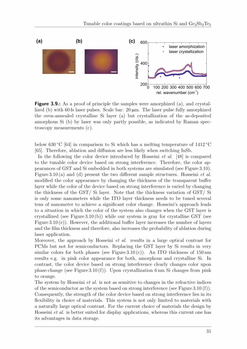
Tunable color coatings based on ultrathin Si and Ge2Sb2Te5
(a) (b)
0 100 200 300 400 500 600 700200
400
600
inte
nsi
ty (
cts.
)
rel. wavenumber (cm-1)
laser amorphization laser crystallization
(c)
Figure 3.9.: As a proof of principle the samples were amorphized (a), and crystal-lized (b) with 60 fs laser pulses. Scale bar: 20µm. The laser pulse fully amorphizedthe oven-annealed crystalline Si layer (a) but crystallization of the as-depositedamorphous Si (b) by laser was only partly possible, as indicated by Raman spec-troscopy measurements (c).
below 630 C [64] in comparison to Si which has a melting temperature of 1412 C[65]. Therefore, ablation and diffusion are less likely when switching InSb.
In the following the color device introduced by Hosseini et al. [48] is comparedto the tunable color device based on strong interference. Therefore, the color ap-pearances of GST and Si embedded in both systems are simulated (see Figure 3.10).Figure 3.10 (a) and (d) present the two different sample structures. Hosseini et al.modified the color appearance by changing the thickness of the transparent bufferlayer while the color of the device based on strong interference is varied by changingthe thickness of the GST/ Si layer. Note that the thickness variation of GST/ Siis only some nanometers while the ITO layer thickness needs to be tuned severaltens of nanometer to achieve a significant color change. Hosseini’s approach leadsto a situation in which the color of the system also changes when the GST layer iscrystallized (see Figure 3.10 (b)) while our system is gray for crystalline GST (seeFigure 3.10 (e)). However, the additional buffer layer increases the number of layersand the film thickness and therefore, also increases the probability of ablation duringlaser application.Moreover, the approach by Hosseini et al. results in a large optical contrast forPCMs but not for semiconductors. Replacing the GST layer by Si results in verysimilar colors for both phases (see Figure 3.10 (c)). An ITO thickness of 150 nmresults e.g. in pink color appearance for both, amorphous and crystalline Si. Incontrast, the color device based on strong interference clearly changes color uponphase-change (see Figure 3.10 (f)). Upon crystallization 6 nm Si changes from pinkto orange.The system by Hosseini et al. is not as sensitive to changes in the refractive indicesof the semiconductor as the system based on strong interference (see Figure 3.10 (f)).Consequently, the strength of the color device based on strong interference lies in itsflexibility in choice of materials. This system is not only limited to materials witha naturally large optical contrast. For the current choice of materials the design byHosseini et al. is better suited for display applications, whereas this current one hasits advantages in data storage.
31

Tunable color coatings based on ultrathin Si and Ge2Sb2Te5
Si-wafer
150 nm Au
GST/Si
40 nm SiO2
5 nm Ti
Si-wafer
100 nm Pt
7 nm GST/Si
ITO
10 nm ITO
(a)
(d)
50
100
150
ITO
thic
kness
(nm
)
amorphousGST
crystallineGST
(b)
50
100
150
ITO
thic
kness
(nm
)
amorphousSi
crystallineSi
(c)
0
5
10
15
GS
T thic
kness
(nm
)
amorphousGST
crystallineGST
(e)
0
5
10
15
Si t
hic
kness
(nm
)
amorphousSi
crystallineSi
(f)
Figure 3.10.: The color of the system introduced by Hosseini et al. (a) is tunableby the thickness of the ITO layer. The simulated color appearances are presentedfor amorphous and crystalline GST (b) and for amorphous and crystalline Si (c)embedded in the layer structure. For comparison the tunable color device based onstrong interference (d) and its simulated color appearance for GST (e) and Si (f)are also shown.
3.5. Conclusion
In conclusion, we introduced a new application for the strong interference effect.Ultrathin phase-change materials and semiconductors on metals can be switchedbetween the amorphous and crystalline phase, associated with a large color change.The reflectance spectra are robust with respect to the angle of incidence of thelight [31, 49]. This is important for color consistency on flexible substrates or fordisplay applications (see Chapter 7). The optical contrast of GST integrated inthis structure is enhanced, and reversible color switching between blue and graywith femtosecond laser pulses is demonstrated. Besides display applications withoutpower consumption in the static mode, these layer structures are also interestingfor applications in optical data storage devices. Pure GST, for example, does notexhibit the required optical contrast for wavelengths around 405 nm and has beenreplaced by Ge-rich PCMs for third-generation storage media such as Blu-ray disks.In Figure 3.11, we demonstrate that optimizing the thickness of GST and SiO2 on
32
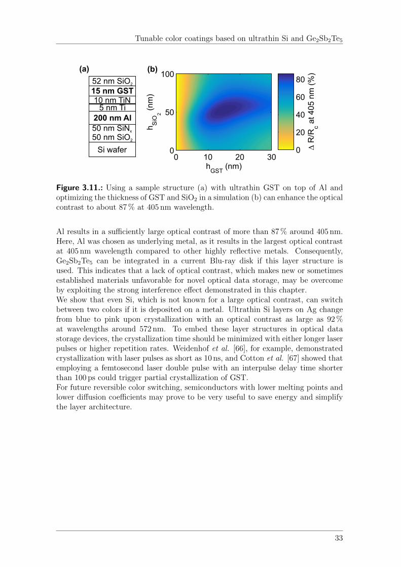
Tunable color coatings based on ultrathin Si and Ge2Sb2Te5
200 nm Al
10 nm TiN15 nm GST52 nm SiO2
50 nm SiNx
50 nm SiO2
Si wafer
5 nm Ti
(a)
hGST
(nm)
hS
iO2
(nm
)
(b)
0 10 20 300
50
100
∆ R
/Rc a
t 405 n
m (
%)
0
20
40
60
80
Figure 3.11.: Using a sample structure (a) with ultrathin GST on top of Al andoptimizing the thickness of GST and SiO2 in a simulation (b) can enhance the opticalcontrast to about 87 % at 405 nm wavelength.
Al results in a sufficiently large optical contrast of more than 87 % around 405 nm.Here, Al was chosen as underlying metal, as it results in the largest optical contrastat 405 nm wavelength compared to other highly reflective metals. Consequently,Ge2Sb2Te5 can be integrated in a current Blu-ray disk if this layer structure isused. This indicates that a lack of optical contrast, which makes new or sometimesestablished materials unfavorable for novel optical data storage, may be overcomeby exploiting the strong interference effect demonstrated in this chapter.We show that even Si, which is not known for a large optical contrast, can switchbetween two colors if it is deposited on a metal. Ultrathin Si layers on Ag changefrom blue to pink upon crystallization with an optical contrast as large as 92 %at wavelengths around 572 nm. To embed these layer structures in optical datastorage devices, the crystallization time should be minimized with either longer laserpulses or higher repetition rates. Weidenhof et al. [66], for example, demonstratedcrystallization with laser pulses as short as 10 ns, and Cotton et al. [67] showed thatemploying a femtosecond laser double pulse with an interpulse delay time shorterthan 100 ps could trigger partial crystallization of GST.For future reversible color switching, semiconductors with lower melting points andlower diffusion coefficients may prove to be very useful to save energy and simplifythe layer architecture.
33


Aluminum-induced crystallization of ultrathin Si films
4. Aluminum-induced crystallizationof ultrathin Si films
This chapter focuses on the synthesis of ultrathin polycrystalline Si films onpolyimide substrates. The challenge lies in the considerably lower servicetemperature of Kapton® E compared to the crystallization temperature ofbulk Si. The aluminum-induced layer exchange mechanism is well-knownto reduce the crystallization temperature of Si. Here, a parametric studyis conducted to determine the deposition parameters of Si and Al that leadto a reduction of the crystallization temperature of Si below 400 C. Theresults are of great interest for applications such as solar cells or thin-filmtransistors based on thin polycrystalline Si films on plastic substrates.
4.1. Introduction
Static color coatings based on the structures introduced in Chapter 2, or tunablecolor coatings based on ultrathin Si which were described in Chapter 3, are poten-tial candidates as decorative coating. Moreover, ultrathin amorphous and polycrys-talline Si (poly-Si) films are heavily employed in microelectromechanical systems(MEMS) [68], in solar cells [3, 69], or transistors [70–72]. The loss of integrity of athin Si film might lead to failure of the entire device. Therefore, it is of great im-portance to determine the cohesive and adhesive properties of ultrathin amorphousand poly-Si films on flexible substrates. Generally, flexible substrates are made ofplastic with a limited service temperature which, for e.g. Kapton® E polyimidesubstrates, lies between 360 C and 410 C [73]. However, Si crystallizes at 800 C[17]. Therefore, a method to crystallize Si at temperatures below 400 C is required.Laser crystallization of ultrathin Si films below 100 nm is difficult due to the largepenetration depth of light in Si (see Figure 4.1). The light intensity at 532 nm wave-length decreases to 1/e at a penetration depth of e.g. 65 nm in amorphous, and312 nm in poly-Si. Consequently, only a small part of the light is absorbed for Sifilms below 100 nm thickness. On the one hand, high light power is required tocrystallize the Si films. On the other hand, this light power damages the underlyingplastic substrate. Moreover, laser crystallization limits the crystalline Si film to asmall area and results in an interface of amorphous and crystalline Si which inducesstress concentrations. Therefore, here, laser-induced Si crystallization is dismissed.Other methods, such as substrate annealing below 400 C, and ion bombardment ofSi films during sputter deposition, do not result in crystalline Si.As an alternative approach metals in contact with amorphous Si can induce crys-
tallization of the amorphous semiconductor at temperatures as low as 150 C [74].
35

Aluminum-induced crystallization of ultrathin Si films
300 400 500 600 700 8000
200
400
600
800
1000
pe
ne
tra
tio
n d
ep
th (
nm
)
wavelength (nm)
amorphous Sipoly−Si
Figure 4.1.: Simulated light penetration depth as a function of wavelength of amor-phous and polycrystalline Si. The refractive indices of amorphous and poly-Si weretaken from literature [38].
Various metals have been found to promote crystallization at reduced temperaturesas compared to bulk crystallization temperatures. Si in contact with transitionmetals such as Ni, Pd, Pt, or Cu forms multiple compounds and a so-called metal-induced lateral crystallization (MILC) process is often realized for such systems.Post-transition metals such as Al, In, Sn, Pb, Sb, or Bi constitute eutectic binarysystems with Si and a metal-induced layer exchange (MILE) process can often beobserved. Metal-induced crystallization (MIC) temperatures of Si in contact withpost-transition metals are generally lower than that of Si in contact with transitionmetals [75]. Here, we use Al to induce crystallization of ultrathin Si films. The
c-SiAla-Si
grainboundary
a-Sia-SiAl
crystallizedSi
layer exchangeinitial state wetting crystallization
(a) (b) (c) (d)
Figure 4.2.: Illustration of the aluminum-induced layer exchange (AILE) mecha-nism. (a) In the initial state, an Al layer is covered with an amorphous Si (a-Si)film. (b) Annealing of the films results in amorphous Si wetting at Al grain bound-aries. (c) Above a temperature of 140 C Si crystallizes at the Al grain boundaries.(d) The aluminum-induced layer exchange mechanism is completed and crystallineSi (c-Si) is covered with an Al film.
36

Aluminum-induced crystallization of ultrathin Si films
mechanism is illustrated in Figure 4.2 and described as follows [75]: Amorphous Siwets high-angle Al grain boundaries (see Figure 4.2 (b)) and crystallizes exclusivelythere above a critical temperature of about 140 C (see Figure 4.2 (c)). The growthand crystallization of Si at the original grain boundaries leads to compressive stressin the Al layer and tensile stress in the amorphous Si film. Consequently, a diffu-sion potential gradient is formed for the Al atoms and they start to diffuse into theamorphous Si film which has a large free volume (see Figure 4.2 (c)). The resultingAl plums in amorphous Si move upwards and grow in size as more and more Alatoms diffuse into the Si film. Hence, during crystallization the Al and Si layersexchange their initial position (see Figure 4.2 (d)).Small variations in the microstructure of the Al film might lead to different crystal-lization temperatures and crystallization behaviors [76, 77]. Moreover, the substratematerial, the Al-Si interface, the layer sequence, and the layer ratio have a large in-fluence on the crystallization behavior [76, 78, 79]. Researchers have investigated theinfluence of various fabrication methods such as electron beam evaporation, sputterdeposition, or thermal evaporation [80]. Moreover, Chu et al. [81] have shown thatthe dc sputtering power during Al deposition influences the film stress, the surfaceroughness, and the crystal quality. However, to our knowledge, the influence ofsputter parameters on the crystallization temperature of Si is unknown.Here, we investigate the crystallization time and temperature of Si films in contactwith Al films sputtered at different dc powers and different Ar pressures. Moreover,the influence of substrate bias during both, Si sputtering and Al sputtering is ex-amined. The aim of this study is to determine the sputter parameters for whichthe crystallization temperature of Si on Kapton® E substrates is reduced below themaximum service temperature of the Kapton® E sheet.
4.2. Materials and Methods
Thin films were fabricated by magnetron sputter deposition (PVD Products) witha base pressure of less than 8·10−5 Pa. Polyimide sheets (Kapton® E from DuPont)with a thickness of 50µm were used as substrates. Prior to deposition, the polyimidesheets were cleaned in acetone (at least 15 min) and isopropanol (at least 15 min) inan ultrasonic bath. Subsequently, they were pre-shrunk in a furnace at 200 C forat least 6 hours to remove trapped residual solvents. During sputter deposition, thesubstrate was rotated with 30 rpm in order to achieve a homogeneous film thickness.Various sputter parameters were used to deposit 150 nm Al on top of 150 nm Si filmson a polyimide substrate. Note that the samples were not exposed to air in betweenSi and Al sputter deposition. For each sample only one parameter was changed ata time such that the influence on the crystallization temperature could be observed.Table 4.1 gives an overview of the deposition parameters. Thin films in the table arearranged according to the power they were deposited at.Thermal annealing at various annealing temperatures (250 C, 300 C, and 350 C)
and for various annealing durations (1 h, 4 h, 10 h, and 24 h) was employed to achievecrystallization of the Si films. Annealing was performed in a vacuum furnace at apressure of 2 Pa.The cross sections of the thin films were polished by a Hitachi IM4000 broad ion
37

Aluminum-induced crystallization of ultrathin Si films
Table 4.1.: Al and Si thin film deposition parameters, with magnetron power P , Arpressure p, rf substrate bias, and Ar flow.
Al deposition parameters Si deposition parametersP p rf Bias flow P p rf Bias flow
(W) (Pa) (W) (sccm) (W) (Pa) (W) (sccm)100 W
100 2.67 - 20 300 0.40 - 502.67 Pa
100 W100 0.67 - 20 300 0.40 - 50
0.67 Pa
200 W200 2.67 - 20 300 0.40 - 50
4.00 Pa
200 W200 0.67 - 20 300 0.40 - 50
0.67 Pa
300 W300 2.67 - 20 300 0.40 - 50
2.67 Pa
300 W300 0.67 - 20 300 0.40 - 50
0.67 Pa
300 W300 2.67 30 20 300 0.40 - 500.67 Pa
rf bias (Al)
300 W300 0.67 - 20 300 0.40 30 500.67 Pa
rf bias (Si)
38

Aluminum-induced crystallization of ultrathin Si films
beam (BIB) miller. Firstly, the films on the Kapton® E substrates were attached tothe polished side of a Si wafer piece by silver paste. Two or three films were sand-wiched together such that they were polished in one run. The polished side of thewafer faced the films on the polyimide substrates. To minimize the polishing timein the BIB miller, all Kapton® E substrates were arranged parallel to each otherand their edges were slightly higher than the edge of the Si wafer. Hence, only thepolyimide substrates and the films, but not the Si wafer were polished. Secondly,the Si wafer piece was mounted to a modified SEM stub such that the cross-sectionalarea which was polished was arranged parallel to the stub surface. Finally, the sam-ples were aligned in the BIB miller and the parameters during milling were 6 kVacceleration voltage and 0.1 sccm Ar flow.Imaging of the prepared cross sections was performed utilizing a FEI Magellan 400scanning electron microscope at 10 kV. Secondary electrons were detected as theimage contrast of back-scattered electrons of Al and Si atoms is little because of thesimilar atomic number.The surfaces of as-deposited and annealed films were investigated with a confocallight microscope (WITec CRM200). Raman spectra were obtained from measure-ments with a confocal Raman system (WITec CRM200) with 532 nm excitation, a100x objective lens with numerical aperture NA=0.9, and a fiber-coupled gratingspectrometer (2400 lines/mm). The laser intensity at the sample surface was reducedto 35.5µW/µm2 to minimize sample heating.
4.3. Results
Figure 4.3 presents surface optical micrographs of the samples prepared by varioussputtering powers and sputtering pressures. The optical appearance of Al is muchbrighter than that of Si. Thus, the metal-induced layer exchange mechanism wascompleted as soon as the color of the optical micrographs changed from blue tolight blue. For all samples, a higher annealing temperature and a longer annealingduration led to an increase of light blue colors of the optical micrographs.However, a complete layer exchange mechanism was accomplished for only threeof the eight samples sputtered at different deposition parameters. The AILEmechanism was achieved for an Ar pressure of 0.67 Pa, a dc sputter power of100 W and 300 W, as well as an rf substrate bias during Al deposition. Still, smalldark dots in the micrographs of these three samples indicate that some Si did notexchange the layer position.Rf substrate biasing during Al deposition resulted in a completed AILE mechanism
at the lowest annealing temperature and the shortest annealing time. Here, only4 h annealing at 250 C were sufficient to crystallize the Si film. However, applyingan rf substrate bias during Si and Al sputtering was challenging. The plasma wasnot stable and hence, reproduction of the sample was difficult. To some extentthe plasma existed at a limited part of the sample and rotated together with thesubstrate holder. Moreover, applying an rf substrate bias sometimes resulted insparks at the substrate and black damaged Kapton® E sheets.
39

Aluminum-induced crystallization of ultrathin Si films
As dep.
100 W2.67 Pa
24 h350 °C
10 h300 °C
4 h250 °C
1 h 250 °C
100 W0.67 Pa
200 W4.00 Pa
200 W0.67 Pa
300 W0.67 Pa
30 W rf bias (Al)
300 W0.67 Pa
30 W rf bias(Si)
300 W2.67 Pa
300 W0.67 Pa
80 μm
Figure 4.3.: Surface images of sputtered Al and Si films before and after variousannealing durations and temperatures. Initially, the Si film was sputtered on top ofthe Al film. Al has a larger reflectance than Si and a bright blue color indicates acomplete AILE mechanism. These images are marked with a green frame.
40

Aluminum-induced crystallization of ultrathin Si films
An Ar pressure of 0.67 Pa and a dc sputter power of 100 W and 300 W duringsputter deposition of the Al film led to crystallization of Si after 10 h annealing at300 C. Also, the other samples exhibit bright spots in the optical micrographs atthis annealing temperature and duration which indicates that some Al atoms dif-fused into the Si top film. However, a complete layer exchange was not achieved.Exemplarily, Figure 4.4 depicts Raman spectra of the samples sputtered at 0.67 PaAr pressure and 300 W dc power annealed to different temperatures. The as-deposited sample (dark blue graph) exhibits a broad amorphous peak at 480 cm−1.Annealing the sample to 250 C for 1 h and 4 h (bright blue and violet graphs) re-sulted in a small intensity Raman peak at 520 cm−1 and the broad peak at 480 cm−1
decreased compared to the peak of the as-deposited sample. This indicates that Sipartly crystallized. Further annealing of the sample to 300 C for 10 h (rose graph)led to a decrease of the crystalline Si Raman peak at 520 cm−1 and the amorphous SiRaman signal disappeared. Determining the Raman signal of the sample annealedto 350 C for 24 h yields two different spectra: (i) The Raman measurement of oneof the dark dots visible in the micrograph in Figure 4.3 (red graph) exhibits a crys-talline Si signal. As the AILE mechanism was completed no underlying Al couldabsorb the laser light and consequently, the observed background noise originatedfrom the polyimide substrate. (ii) Raman spectrum of the top Al layer (orangegraph) did not result in any signal.
350 400 450 500 550 600
280
300
320
3000
3500
4000 as dep. 1 h 250 °C 4 h 250 °C 10 h 300 °C 24 h 350 °C
(black dot) 24 h 350 °C
inte
nsity (
cts
.)
rel. wavenumber (cm-1)
Figure 4.4.: Raman spectra of samples deposited at 300 W dc sputter power and0.67 Pa Ar pressure at various annealing temperatures and durations are shown.
41

Aluminum-induced crystallization of ultrathin Si films
As dep.
100 W2.67 Pa
24 h350 °C
10 h300 °C
4 h250 °C
1 h 250 °C
100 W0.67 Pa
200 W4.00 Pa
200 W0.67 Pa
300 W0.67 Pa
30 W rf bias (Al)
300 W0.67 Pa
30 W rf bias(Si)
300 W2.67 Pa
300 W0.67 Pa
400 nm
Figure 4.5.: Cross-sectional SEM micrographs of sputtered Al and Si films beforeand after various annealing times and temperatures. Different sputter parameterswere used for the Al films. The last row of the table shows cross sections of Al andSi films where 30 W rf bias was applied during Si deposition.
42
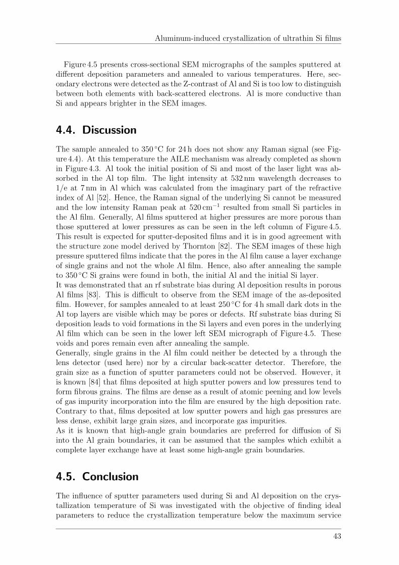
Aluminum-induced crystallization of ultrathin Si films
Figure 4.5 presents cross-sectional SEM micrographs of the samples sputtered atdifferent deposition parameters and annealed to various temperatures. Here, sec-ondary electrons were detected as the Z-contrast of Al and Si is too low to distinguishbetween both elements with back-scattered electrons. Al is more conductive thanSi and appears brighter in the SEM images.
4.4. Discussion
The sample annealed to 350 C for 24 h does not show any Raman signal (see Fig-ure 4.4). At this temperature the AILE mechanism was already completed as shownin Figure 4.3. Al took the initial position of Si and most of the laser light was ab-sorbed in the Al top film. The light intensity at 532 nm wavelength decreases to1/e at 7 nm in Al which was calculated from the imaginary part of the refractiveindex of Al [52]. Hence, the Raman signal of the underlying Si cannot be measuredand the low intensity Raman peak at 520 cm−1 resulted from small Si particles inthe Al film. Generally, Al films sputtered at higher pressures are more porous thanthose sputtered at lower pressures as can be seen in the left column of Figure 4.5.This result is expected for sputter-deposited films and it is in good agreement withthe structure zone model derived by Thornton [82]. The SEM images of these highpressure sputtered films indicate that the pores in the Al film cause a layer exchangeof single grains and not the whole Al film. Hence, also after annealing the sampleto 350 C Si grains were found in both, the initial Al and the initial Si layer.It was demonstrated that an rf substrate bias during Al deposition results in porousAl films [83]. This is difficult to observe from the SEM image of the as-depositedfilm. However, for samples annealed to at least 250 C for 4 h small dark dots in theAl top layers are visible which may be pores or defects. Rf substrate bias during Sideposition leads to void formations in the Si layers and even pores in the underlyingAl film which can be seen in the lower left SEM micrograph of Figure 4.5. Thesevoids and pores remain even after annealing the sample.Generally, single grains in the Al film could neither be detected by a through thelens detector (used here) nor by a circular back-scatter detector. Therefore, thegrain size as a function of sputter parameters could not be observed. However, itis known [84] that films deposited at high sputter powers and low pressures tend toform fibrous grains. The films are dense as a result of atomic peening and low levelsof gas impurity incorporation into the film are ensured by the high deposition rate.Contrary to that, films deposited at low sputter powers and high gas pressures areless dense, exhibit large grain sizes, and incorporate gas impurities.As it is known that high-angle grain boundaries are preferred for diffusion of Siinto the Al grain boundaries, it can be assumed that the samples which exhibit acomplete layer exchange have at least some high-angle grain boundaries.
4.5. Conclusion
The influence of sputter parameters used during Si and Al deposition on the crys-tallization temperature of Si was investigated with the objective of finding idealparameters to reduce the crystallization temperature below the maximum service
43

Aluminum-induced crystallization of ultrathin Si films
temperature of Kapton® E substrates. Here, the film thickness ratio of Si and Alwas 1:1.Several sputter parameters are advantageous to complete a layer exchange mecha-nism at low temperatures:
• Low Ar pressure during Al sputtering is preferred. The films are denser andthe diffusion of Si into the grain boundaries occurs at lower temperatures.
• High Al sputter powers lead to Si crystallization at lower annealing tempera-tures compared to Si on Al films sputtered at low power.
• Rf substrate bias during Si deposition is not recommended because it leads tovoid formation in the Si film and pores in the underlying Al film. Moreover,the layer exchange is not feasible for annealing temperatures up to 350 C.
• Rf substrate bias during Al deposition results in a complete layer exchangeof Si and Al films at the lowest annealing temperature (4 h at 250 C). How-ever, the plasma at the substrate is not stable during sputtering and in someextent sparks at the substrate are built which might damage the Kapton® Esubstrates.
In conclusion, Al should be sputtered at low Ar pressures (0.67 Pa) and at high dcpowers (300 W). Substrate bias causes reduced crystallization temperatures but isnot recommended for the PVD sputter tool used here, as the plasma is unstable.
44

Mechanical properties of amorphous and crystalline Si films
5. Mechanical properties ofamorphous and crystalline Si films
In this chapter, fragmentation and buckling of 8-103 nm thin amorphous andpolycrystalline (poly-) Si films on polyimide substrates have been studied byin situ light microscopy, Raman spectroscopy, and resistance measurements.Generally, a smaller film thickness and a compressive residual stress delaysthe fracture of the film. The fracture strength of poly-Si films is larger com-pared to that of amorphous Si films while the adhesion to the substrate isbetter for amorphous Si compared to poly-Si. The onset delamination asa function of film thickness differs for the two phases and is described bytwo different models. Thin-film models for fracture toughness (amorphousSi: K1C=1.4± 0.22 MPa m0.5, poly-Si: K1C=3.36± 1.37 MPa m0.5) are ap-plied, discussed, and found to be consistent with literature values. Moreover,the mechanical properties of the insulator structure introduced in Chapter 2based on ultrathin Si top layers of different thicknesses are investigated. Thecontent of this chapter is based on the work published in Acta Materialia[85].
5.1. Introduction
Ultrathin Si films in the nanometer-range are, amongst others, implemented in solarcells [3, 69], microelectromechanical systems (MEMS) [68], transistors [70–72], orinterference coatings [31, 86]. The functionality of the devices relies on their me-chanical integrity during service life. Strain due to bending or torsion of deviceson flexible substrates or thermal stress could lead to failure. Fracture toughness,which corresponds to the resistance to the propagation of cracks is a relevant factorwhen it comes to brittle materials such as Si. Many researchers have evaluated thefracture toughness of Si samples with different crystallographic phases and geome-tries. Poly-Si films in the micrometer range thickness were studied extensively andfracture toughness values between 1.1 MPa m0.5 and 4.5 MPa m0.5 were reported [87–89]. The fracture toughness of single crystalline specimens lies around 0.8 MPa m0.5
and 1.3 MPa m0.5 [90, 91]. Ballarini et al. investigated the fracture toughness ofmicrometer-thick amorphous Si. They determined a value of 1.0 MPa m0.5 [92].However, they assumed that the Young’s modulus of amorphous Si is the sameas that of poly-Si, which is unlikely [93, 94]. Waller et al. determined an energyrelease rate of 16 J/m2 for a 230 nm amorphous Si film (aSi:H) which correspondsto a fracture toughness of 1.2 MPa m0.5 [95].To our knowledge there is a lack of information on the mechanical properties of
45

Mechanical properties of amorphous and crystalline Si films
nanometer-sized Si films. It can be expected that they have much better cohesiveand adhesive properties compared to micrometer thick films because of a size-effect.It was shown that nanometer-sized Si layers on various substrate materials exhibitbright color appearance and can be used as static color coatings (see Chapter 2).Moreover, ultrathin Si films deposited on metals switch their color upon amorphiza-tion and crystallization, respectively [46]. Consequently, it is of interest to comparethe mechanical properties of amorphous and crystalline Si films of various thick-nesses for the application as tunable color coating. In this study, both gaps arefilled by investigating the fracture behavior of 8-103 nm thick amorphous and poly-Si films on polyimide substrates. The onset strain of fragmentation and buckling,the fracture strength, and the fracture toughness are obtained from uniaxial tensiletests and, these values are compared to literature values where available.
5.2. Materials and Methods
Sample fabricationThin Si films were fabricated by magnetron sputter deposition (PVD Products)with a base pressure of less than 8·10−5 Pa. Polyimide sheets (Kapton® E fromDuPont) with a thickness of 50µm were used as substrates. Prior to depositionthe polyimide sheets were cleaned in acetone (at least 15 min) and isopropanol(at least 15 min) in an ultrasonic bath and subsequently annealed in a furnace at200 C for at least 6 hours. During sputter deposition the substrate was rotatedwith 30 rpm in order to achieve a homogeneous film thickness. Amorphous Si filmswere fabricated by alternating current sputter deposition using a power of 300 W,a pressure of 0.67 Pa and an argon flow of 50 sccm. This resulted in 8 nm, 18 nm,25 nm, 43 nm, and 96 nm thick amorphous Si films on Kapton® E. For in situresistance measurements during straining amorphous Si films with a thin conductivePt capping layer were sputtered without breaking the vacuum in between. A directcurrent power of 100 W, a pressure of 0.67 Pa, and an argon flow of 20 sccm wereused for Pt.Poly-Si was fabricated from amorphous Si by an aluminum-induced layer exchange(AILE) mechanism as described in Chapter 4. The crystallization temperature ofSi on Kapton® E must be below 400 C because the maximum service temperatureof Kapton® E is between 360 C and 410 C [73]. Compared to the ideal sputterparameters of Al and Si derived in Chapter 4 we further improved some parametersto ensure a continuous poly-Si film which crystallizes at low temperatures.In this study, the film thickness of Al was always slightly thinner than that of Si(ratio approx. 5:6) in order to ensure a continuous poly-Si film [78]. First, Alwas sputtered onto Kapton® E with a power of 300 W at 0.67 Pa and with an Arflow of 10 sccm. Second, the film was exposed to air for 5 min such that a thinAl oxide layer was formed [96]. Third, amorphous Si was sputtered onto the Allayer. The rf power was adjusted to 300 W, the pressure was set to 0.40 Pa, andthe Ar gas flow was 50 sccm. After annealing the samples in a vacuum furnace(2 Pa) at 400 C for 18 h the layer exchange was completed. This was confirmed bycross-sectional high resolution scanning electron microscope (SEM) images (FEIMagellan 400 FEG XHR-SEM). In a last step the Al was etched according to [97]
46

Mechanical properties of amorphous and crystalline Si films
(a) as dep.
18 h at 400°C
300 nm
18 h at 400°C; Al etched
(b)
(c)
Si
Al
Al
Si
Si
Figure 5.1.: Cross section SEM images of sputtered Al and Si film on Kapton® Ebefore (a) and after annealing ((b) and (c)). On top of the films silver particles canbe seen which are due to the cross section preparation process. After wet-chemicaletching of the Al film (c), small Si crystallites remain on top of the continuouspoly-Si layer.
with 16 H3PO4:1 HNO3:1 HAc:2 H2O at 50 C. Finally, the poly-Si films on polyimidehad a thickness of 32 nm, 40 nm, 45 nm, 100 nm, and 103 nm. Typical SEM cross sec-tional micrographs during the AILE mechanism are depicted exemplarily for 103 nmSi in Figure 5.1 (a)-(c). The as-deposited Al and amorphous Si films on Kapton® Eare shown in Figure 5.1 (a). In Figure 5.1 (b), the AILE mechanism was completedand the Si was crystalline after annealing. The film thickness of the as-depositedSi film was slightly larger than the Al film thickness such that some crystallineSi particles stayed in the Al film (see Figure 5.1 (b)). After etching the Al film acontinuous poly-Si film remains covered with some Si crystallites (see Figure 5.1 (c)).
CharacterizationThe residual stress of the Si films was determined by two different methods. Foramorphous Si the curvature of the polyimide substrates with the Si films wasmeasured by optical microscopy and the residual stress was calculated using theStoney equation [98]. For poly-Si films this method was not reliable because thelong exposure to 400 C results in a plastic deformation of the polyimide substrate.Consequently, the curvature did not originate only from the film but also fromthe substrate. Here, the stress was calculated from Raman spectra obtained frommeasurements with a confocal Raman system (WITec CRM200) with 441 nm exci-tation, a 100x objective lens with numerical aperture NA=0.9, and a fiber-coupledgrating spectrometer (2400 lines/mm). The laser intensity at the sample surfacewas reduced to 35.5µW/µm2 to minimize sample heating. The peak positions ofthe Si spectra were fitted with a MATLAB routine employing Lorentzian curves.For each film, 4 line scans with 20 spectra each were measured and the Si peak
47

Mechanical properties of amorphous and crystalline Si films
positions were averaged.For uniaxial tensile tests, the samples were mounted into a tensile machine (Kamm-rath & Weiss GmbH) equipped with a 200 N load cell. Each sample was 5 mmwide and the gage length l was 14 mm (resistance measurement) or 30 mm (opticalmicroscopy and Raman spectroscopy measurement). The corresponding strain rateswere 10−4 sec−1 and 4.7·10−5 sec−1, respectively. Crack patterns and crack distancesof the films were investigated with a confocal light microscope (WITec CRM200)and simultaneous stepwise loading of the sample. The mean crack distance L wasdetermined with a MATLAB routine [99] based on optical micrographs.In situ resistance measurements of amorphous Si with a thin Pt capping layerwere performed with an electrical resistance module. During uniaxial loading thecurrent was minimized (100 mA) to prevent heating of the sample and the changeof voltage was recorded. Platinum has the advantage that it can be deposited asa continuous thin film so that the film thickness is small enough that the crackingbehavior of Si is not influenced. Cracks in the Si film leads to instantaneous fractureof the platinum top layer due to strain localization [100]. Typically resistancemeasurements are compared to the ideal plastic deformation curve [101, 102]. As Sidoes not exhibit plastic deformation, here the change of resistance is calculated asa function of uniaxial strain in the elastic regime. For this ideal resistance changeR/R0 = (1 + ε)(1 + 2νfε) the Poissons ratio of the film νf and the applied uniaxialstrain ε need to be considered. The change of the normalized electrical resistanceR/R0 with the initial resistance R0 of the film before loading was measured fordifferent film thicknesses. This method could not be applied for poly-Si becausethe Si crystallites on top of the poly-Si film prevent a smooth substrate surfacefor the Pt top layer. Hence, Raman spectroscopy was applied to spots where noSi crystallites cover the poly-Si film. The adjustments of the Raman spectroscopewere identical to those for measuring the residual stress. Line scans were performedfor various strains always at the same spot to record the change of the peak positionas a function of strain. Each line scan included 40 spectra which were fitted withLorentzian curves. The resulting peak positions were averaged for each line scan.
5.3. Results
5.3.1. Residual stress
The determined residual stresses σres of the amorphous and poly-Si films are sum-marized in Table 5.1. The residual stress is compressive for all films and varies as afunction of film thickness. The errors of the residual stress of amorphous Si resultfrom error estimations on the determined curvature.Note, that the Pt capping layer may slightly influence the residual stress althoughthe Pt films are very thin. Nevertheless, these films with the Pt capping layer areonly used to determine the onset strain of fragmentation by resistance measurementsto compare the results with the onset strain of fragmentation obtained from opticalmicroscopy.
For poly-Si, the residual stress was calculated from Raman measurements. TheRaman peak of unstrained Si at xr=520 cm−1 was used as a reference for all measure-ments. The AILE mechanism results in an Al doping of the poly-Si films. Energy-
48

Mechanical properties of amorphous and crystalline Si films
Table 5.1.: Residual stress σres of amorphous and poly-Si layers with film thicknessd on Kapton® E.
Amorphous Si Poly-Sid (nm) σres (MPa) d (nm) σres (MPa)
8 -160± 50 32 -620± 22018 -130± 40 40 -50± 31025 -23± 8 45 -500± 15043 -10± 3 100 -530± 15096 -340± 110 103 -850± 80
dispersive X-ray (EDX) spectroscopy measurements showed that the poly-Si filmscontain 5.2 wt. % Al which is homogeneously distributed in the film as confirmed byan EDX mapping. The phase-diagram of Al and Si indicates that this small amountof Al is insoluble in Si. Consequently, the Al content neither influence the Ramanpeak position nor the cohesive and adhesive properties of poly-Si [92]. The residualstress σres is given by [103]: σres=-250 MPa cm−1 ·∆ω with ∆ω = xp− xr, where xpis the average peak position of poly-Si. The specified errors result from averagingat least 4 line scans with 20 Raman measurements each. These errors are largecompared to those of amorphous Si. Figure 5.2 shows a stress map of a poly-Si filmobtained by Raman spectroscopy. The position of the stress map is sketched in anoptical micrograph.
Raman spectra were obtained in an area of 10.0 x 5.4µm2 spaced at intervals of200 nm. Figure 5.2 exhibits the inhomogeneous stress distribution. The residualstress is largely compressive where no crystalline particles cover the film but isnearly completely relaxed where Si crystallites cover the poly-Si film. Consequently,the measured residual stress is strongly dependent on the position on the sample
5 μm
x (µm)
y (µ
m)
0 5 100
1
2
3
4
5
stre
ss σ
(M
Pa)
−1000
−800
−600
−400
−200
0
Figure 5.2.: Optical micrograph image of a 103 nm poly-Si layer with crystalline Siparticles (darker features) on top. In the inset a stress map which was measured byRaman spectroscopy is shown. It indicates that the residual stress of the film is nothomogeneously distributed. The residual stress is compressive where no crystallineparticles can be found and it is relaxed where particles cover the poly-Si layer.
49
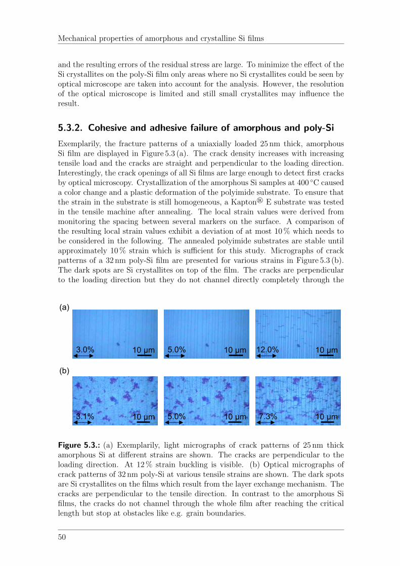
Mechanical properties of amorphous and crystalline Si films
and the resulting errors of the residual stress are large. To minimize the effect of theSi crystallites on the poly-Si film only areas where no Si crystallites could be seen byoptical microscope are taken into account for the analysis. However, the resolutionof the optical microscope is limited and still small crystallites may influence theresult.
5.3.2. Cohesive and adhesive failure of amorphous and poly-Si
Exemplarily, the fracture patterns of a uniaxially loaded 25 nm thick, amorphousSi film are displayed in Figure 5.3 (a). The crack density increases with increasingtensile load and the cracks are straight and perpendicular to the loading direction.Interestingly, the crack openings of all Si films are large enough to detect first cracksby optical microscopy. Crystallization of the amorphous Si samples at 400 C causeda color change and a plastic deformation of the polyimide substrate. To ensure thatthe strain in the substrate is still homogeneous, a Kapton® E substrate was testedin the tensile machine after annealing. The local strain values were derived frommonitoring the spacing between several markers on the surface. A comparison ofthe resulting local strain values exhibit a deviation of at most 10 % which needs tobe considered in the following. The annealed polyimide substrates are stable untilapproximately 10 % strain which is sufficient for this study. Micrographs of crackpatterns of a 32 nm poly-Si film are presented for various strains in Figure 5.3 (b).The dark spots are Si crystallites on top of the film. The cracks are perpendicularto the loading direction but they do not channel directly completely through the
(a)
3.0% 5.0% 12.0%10 μm 10 μm 10 μm
(b)
3.1% 5.0% 7.3%10 μm 10 μm 10 μm
Figure 5.3.: (a) Exemplarily, light micrographs of crack patterns of 25 nm thickamorphous Si at different strains are shown. The cracks are perpendicular to theloading direction. At 12 % strain buckling is visible. (b) Optical micrographs ofcrack patterns of 32 nm poly-Si at various tensile strains are shown. The dark spotsare Si crystallites on the films which result from the layer exchange mechanism. Thecracks are perpendicular to the tensile direction. In contrast to the amorphous Sifilms, the cracks do not channel through the whole film after reaching the criticallength but stop at obstacles like e.g. grain boundaries.
50

Mechanical properties of amorphous and crystalline Si films
(a)
(b)
0.01 0.1
1
10
100
me
an
cra
ck d
ista
nce
L (
µm
)
strain ε
8 nm Si18 nm Si25 nm Si43 nm Si96 nm Si
0.00 0.01 0.02 0.03 0.04 0.05 0.06 0.071.0
1.5
2.0
2.5
3.0
3.5
4.0
no
rma
lize
dre
sis
tan
ceR
/R0
strain
ideal ideal + 5 % deviation 6 nm Pt 8 nm Si + 6 nm Pt 18 nm Si + 6 nm Pt 25 nm Si + 6 nm Pt 43 nm Si + 6 nm Pt 96 nm Si + 16 nm Pt
Figure 5.4.: (a) Mean crack distance as a function of strain for all amorphous Sifilms are shown. The onset strain of fragmentation decreases with increasing filmthickness and the mean crack distance in the saturation regime is linearly dependenton the film thickness of the film. For the error bars only positive deviations of themeasured values are considered because the field of view of the optical microscopeis limited. (b) Normalized resistance curves for all Si films with a Pt top layer areshown. A deviation from the ideal law (dashed lines) indicates the first cracks.
material as it is the case for the amorphous Si films. Here, the cracks slightly deviatefrom straight paths because they have to propagate along the grain boundaries.Figure 5.4 (a) shows the mean crack distance evolution of amorphous Si coatingsfor various thicknesses. The onset strain of fragmentation decreases as a functionof film thickness. In Figure 5.4 (b), the normalized resistance curves of Pt top lay-ers on the amorphous Si films are illustrated. The dashed lines represent the idealresistance change R/R0 = (1 + ε)(1 + 2νfε) (black dashed line) and a deviationof 5 % (red dashed line) from this ideal behavior. A deviation of more than 5 %from the theoretical curve is attributed to cracking as defined by Lu et al. [102].In Figure 5.5 (a) the mean crack distance as a function of strain is depicted for all
51

Mechanical properties of amorphous and crystalline Si films
(a)
(b)
0.01 0.11
10
100
1000
mea
n c
rack d
ista
nce
L (
µm
)
strain ε
32 nm40 nm45 nm100 nm103 nm
0.00 0.02 0.04 0.06
32 nm40 nm45 nm100 nm103 nm
Ram
an p
ea
k p
ositio
n (
a. u.)
strain ε
Figure 5.5.: (a) Mean crack distance of all strained poly-Si films as a function ofapplied strain. (b) The average Raman peak position against applied strain isplotted. For a better overview the data set of each film thickness is shifted in ordinatedirection. For each data point 40 Raman spectra of a line scan are averaged. Withincreasing tensile strain the peak position shifts to smaller wavenumbers until thefirst crack appears. The onset strain of fragmentation is indicated by small dashedrectangles.
poly-Si films. Figure 5.5 (b) illustrates the average Raman peak position for variouspoly-Si film thicknesses as a function of strain. At low strains an increase in strainresults in a shift of the peak position to smaller wavenumbers which correspondsto tensile stress. As soon as the first crack occurs, the film starts to relax and thepeak position shifts to larger wavenumbers. This onset strain of fragmentation isindicated by dashed rectangles for each film thickness.Upon onset strain of fragmentation, stress relaxation occurs in the loading direc-
tion. This relaxation induces an additional mismatch of lateral contraction betweencoating and substrate and leads to compressive stress perpendicular to the loadingdirection. This compressive stress results in delamination of the film. The meandelamination distance is the average spacing between adjacent buckles on individual
52

Mechanical properties of amorphous and crystalline Si films
0.05 0.1 0.15 0.2 0.25
1
10
100
1000
mea
n d
ela
min
ation d
ista
nce
(µm
)
strain ε
amorphous Si:18 nm25 nm43 nm96 nm
poly-Si:32 nm40 nm45 nm100 nm
Figure 5.6.: Mean delamination distance of amorphous and poly-Si.
fragments. For both, amorphous and poly-Si films the mean delamination distancesas a function of strain are presented in Figure 5.6.At low strains the mean delamination distance decreases rapidly as a function of ap-plied strain and saturates at higher strains. Poly-Si films delaminate at lower strainscompared to amorphous Si layers. Generally, the mean delamination distance in-creases as a function of film thickness at high strains. For 8 nm amorphous Si and103 nm poly-Si only the onset strain of delamination but not the mean delaminationdistance was determined because the resolution of the optical microscope was notadequate.
5.3.3. Cohesive and adhesive failure of Si embedded in theinsulator structure
Three different color coatings based on ultrathin amorphous Si were introduced inChapter 2. These sample structures are potential candidates for decorative coatingson both, rigid and flexible substrates. For the latter application it is importantto investigate the cohesive and adhesive properties of ultrathin Si embedded inthese structures. Here, the onset strain of fragmentation and onset strain ofdelamination of the insulator structure with 5 nm, 15 nm, and 25 nm amorphousSi were determined. This structure was investigated because compared to the twoother structures, the insulator structure exhibits bright color appearance not onlyin reflectance but also in transmittance. The same structure as that presented inFigure 2.1 (b) with TiO2 and SiO2 as underlying material is used. Note that thestructure on Kapton® E does not lead to bright color appearance as it is the casefor the structure on a silicon wafer. Some light is transmitted through the Kapton®
E substrate. Consequently, deep absorption resonances on Kapton® E substrateswould be obtained for two instead of one bilayer of SiO2-TiO2. This structure wasused to color glass substrates in reflectance and transmittance (see Figure 2.8).
Figure 5.7 presents optical micrographs of 5 nm (a), 15 nm (b), and 25 nm (c)
53

Mechanical properties of amorphous and crystalline Si films
(a)
(b)
10 μm10 μm
10 μm1.2%
10.4% 20.0%10 μm1.2%
10 μm10.4% 10 μm20.0%
(c)
10 μm1.4%
10 μm10.4% 10 μm20.0%
5 nm Si
80 nm TiO2
90 nm SiO2
15 nm Si
80 nm TiO2
90 nm SiO2
25 nm Si
80 nm TiO2
90 nm SiO2
Figure 5.7.: Light micrographs of crack patterns of 5 nm (a), 15 nm (b), and 25 nm(c) amorphous Si deposited onto the insulator structure introduced in Chapter 2 atdifferent strain values are presented. First cracks in the structure with 5 nm Si areshort and do not channel through the whole film as it is the case for thicker Si films(b) and (c). For all film thicknesses delamination occurs at high strains.
amorphous Si deposited on the insulator structure. In the following, the insulatorstructure with the Si capping layers go by the name of the thickness of the ultrathinSi films. Fragmentation in all three samples is perpendicular to the loading directionand cracks do not appear straight through the layers. In contrast to 15 nm Si (b)and 25 nm (c) Si, first cracks in 5 nm Si (a) are short and do not channel throughthe whole film as soon as they occur which indicates that obstacles exist in thelayer structure. Thicker Si top layers result in larger crack distances than thinner Sifilms which is e.g. visible at 10.4 % strain. All three structures exhibit delaminationat large tensile strains with an onset strain of delamination which depends onthe thickness of the top Si layer (5 nm Si: 16.0 % strain; 15 nm Si: 16.8 % strain;25 nm Si: 17.6 % strain). The mean crack distance as a function of applied strain isplotted in Figure 5.8 for all film thicknesses. No film thickness-dependent trend ofthe onset strain of fragmentation is observable. The insulator structure with 5 nmamorphous Si top layer fractures at lower strains than the other two samples. Thehighest onset strain of fragmentation can be observed for 15 nm Si.The saturated mean fragment lengths decrease with decreasing film thickness andrange from 1µm for 5 nm Si to 2µm for 25 nm. The whole layer stack has athickness between 175 nm and 195 nm. A thickness change of the Si layer of 10 nm
54

Mechanical properties of amorphous and crystalline Si films
0.01 0.1
1
10
100
me
an
cra
ck d
ista
nce
L (
µm
)
strain ε
5 nm Si15 nm Si25 nm Si
Figure 5.8.: Mean crack distance of 5 nm, 15 nm, and 25 nm amorphous Si as afunction of strain. In the saturation regime the mean crack distance depends on thethickness of the Si top layer.
corresponds to only 6 % change of the whole thickness. Consequently, a size-effectof the saturated mean fragmentation lengths is expected to be small.
5.4. Discussion
5.4.1. Residual stress
The Raman mapping in Figure 5.2 illustrates that the residual stress is zero whereSi crystallites cover the poly-Si film. As can be seen in Figure 4.1 the penetrationdepth of the Raman laser (λ=441 nm) into poly-Si is 73 nm (intensity decays to 1/e).Consequently, most of the laser light is absorbed inside the Si crystallites and onlythe residual stress of the crystallites and not of the poly-Si film is measured. Afteretching the Al film these crystallites are free-standing which leads to a completestress relaxation. The stress measurement of Si crystallites cannot be completelyavoided because some crystallites are too small to detect them in the optical mi-croscope. Consequently, the underestimation of the compressive residual stress ofthicker poly-Si films is larger, whereas that of thinner films is smaller.
5.4.2. Onset strain of fragmentation and delamination
The onset strains of fragmentation of amorphous and poly-Si observed with differentmethods are summarized in Figure 5.9. The error bars result from stepwise loadingand correspond to the strain applied between two measurement steps. The strainat onset fragmentation of amorphous Si films with and without Pt top layer is ingood agreement. The onset strains of fragmentation observed by in situ resistancemeasurement are not influenced by the Pt top layer, as it does not prevent the de-tection of the first cracks. Provided, cracks are straight and span the entire width
55

Mechanical properties of amorphous and crystalline Si films
0 20 40 60 80 1000.00
0.01
0.02
0.03
0.04amorphous Si:microscope:
Si Si + Pt
resistance Si + Pt: ideal + 5 % ideal + 10 % ideal + 20 %
poly-Si: microscope Raman
onset
stra
in o
f fr
agm
enta
tion ε
on
film thickness d (nm)
Figure 5.9.: Onset strain of fragmentation determined by various methods for allamorphous and poly-Si layers.
of the sample, the resistively determined onset strains of fragmentation are moreprecise. First cracks outside the field of view are not recorded optically but cause asignificant increase of the resistance. Here, the intersection of the resistance curveswith the 5 %, 10 %, and 20 % deviations from the ideal resistance change are plottedas onset strain of fragmentation. However, the magnitude of the deviation fromthe ideal behavior affects the onset strain of fragmentation only little. AmorphousSi is very brittle and as soon as a crack forms it channels through the whole filmsuch that the resistance increases drastically. The surprisingly large onset strain offragmentation of the 96 nm amorphous Si film observed by resistance measurementcan be explained by a 16 nm thick Pt film instead of 6 nm as it was the case for allother amorphous Si films. First cracking in the Si film may not induce cracks in the16 nm thick Pt top layer due to plastic deformation.The onset strains of fragmentation of poly-Si measured by two different methods
are in good agreement. However, both measurement methods are limited to smallfields of view and cracks outside this view are not detected. Hence, the onset strainof fragmentation of poly-Si films might be slightly overestimated. Nevertheless, itcan be concluded that poly-Si films crack at higher strain than amorphous Si layers.This has two reasons: (i) Materials property: It is generally accepted that annealingreduces the density of defects. The first crack is formed as soon as the local stressexceeds the lowest fracture strength of a defect. Consequently, fewer defects increasethe probability of larger onset strains of fragmentation. (ii) System property: Theresidual stress of poly-Si films is more compressive than that of the amorphous Silayers. This large compressive stress helps to delay the onset strain of fragmentationof poly-Si. To calculate the onset strain of fragmentation εonr of a coating whichdoes not exhibit residual stress from the measured onset strain of fragmentation εonthe residual stress σres = Efεres needs to be considered : εonr = εon + σres/Ef . Thesecond reason is more significant as sputter defects may be reduced by annealing
56

Mechanical properties of amorphous and crystalline Si films
sample
cracks buckle
delamination
(a)
(b)
buckle-limitedpoly-Si
strain energy-limitedamorphous Si
ε<εd ε<εd
d
schematic topview
ε>εε>εd
0 20 40 60 80 100 1200.00
0.05
0.10
0.15
0.20 ε
b ~ d
2
b=840 nm
amorphous Si poly-Si
fit: strain energy buckle
parameter study:
G0=100 mJ/m
2
G0=10 mJ/m
2
b=2500 nm b=280 nm
onse
t st
rain
of d
ela
min
ation
εo
n
film thickness d (nm)
εsed
~ d-0.5
G0=33 mJ/m
2
0 20 40 60 80 100 1200.00
0.05
0.10
0.15
0.20
buckle-limited
strain energy criteria
εsed
∼ d -0.5
εb ∼ d
2
onse
t st
rain
of dela
min
atio
n
film thickness d (nm)
Figure 5.10.: (a) Strain at onset delamination for amorphous and poly-Si films.Amorphous Si adheres well to the polyimide film and the onset strain of delaminationdecreases as a function of film thickness. The data is modeled by the strain energycriterion and results G0=33 mJ/m2 as fit parameter. Poly-Si films delaminate atlower strains and the data is fitted by buckle delamination. Here, the fit parameteris the buckle width b=840 nm. For comparison, graphs with differentG0, respectivelyb, are plotted to show the sensitivity to the fit parameters. (b) Schematic drawing ofthe two delamination models. When the onset strain of strain energy delaminationεsed exceeds the onset strain of buckle delamination εb, buckling is expected.
but the AILE mechanism may lead to other defects such as small Al particles insidethe poly-Si film.In Figure 5.10 (a), the onset strains of delamination of amorphous and poly-Si films
are depicted. Two different failure modes may induce delamination: Buckle-limiteddelamination and delamination that follows the strain energy criterion. Delamina-tion that is evaluated by the strain energy criterion is called strain energy delam-
57

Mechanical properties of amorphous and crystalline Si films
ination in the following. Optically, the two different delamination modes are notdistinguishable because both, strain energy and buckle delamination, start at thefragmentation boundaries at the location of maximal compressive stress. However,buckle delamination indicates a weak adhesion of the coating to the substrate andthe onset strain of delamination as a function of film thickness differs for both mod-els.The film thickness dependence on the tensile strain εten for both cases can be calcu-lated if the residual stress is considered and the transverse compressive strain εcom isderived from the tensile strain εten (εcom=(νs-νf )·εten). For the onset strain of strainenergy delamination εsed the expression follows [104]:
εsed =
√2G0
(1− ν2f
)Ef (νs − νf )2
d−0.5 −σres
(1− ν2f
)Ef (νs − νf )
, (5.1)
with Ef and νf the Young’s modulus and the Poisson’s ratio of the film(Ef=80 GPa and νf=0.22 for amorphous Si [93]; Ef=170 GPa and νf=0.22 for poly-Si [16]), νs the Poisson’s ratio of the substrate which we assume to be the same asthe one of Kapton® HN (νs=0.34 [73]) and G0 the energy release rate of the film.For the case of buckle delamination [105] buckling occurs as soon as the onset strainof buckle delamination εb attains the value:
εb =π2
12b2(νs − νf )d2 −
σres(1− ν2f
)Ef (νs − νf )
, (5.2)
where b is half the buckle width. When the onset strain of strain energy delami-nation εsed exceeds the onset strain of buckle delamination εb, buckling is expected(see Figure 5.10 (b)).Generally, poly-Si starts to delaminate at lower strains than amorphous Si. Thisgives evidence that the adhesion to the substrate is worse which might be causedby the Al-induced layer exchange mechanism. Moreover, the strain at onset delam-ination increases as a function of film thickness for poly-Si, while it decreases foramorphous Si. This indicates that the delamination of amorphous Si films follows thestrain energy criterion while thin poly-Si films are buckle-limited. In Figure 5.10 (a)both, buckle and energy strain delamination models are fitted to the data. Here,the residual stress is taken as fit parameter to compare it to the determined residualstress calculated from the curvature of substrate and amorphous Si and calculatedfrom the Raman peak position of poly-Si. For amorphous Si, the fit of the strainenergy delamination model yields an energy release rate G0=33 mJ/m2 and a com-pressive stress σres=-400 MPa. The compressive stress is slightly larger than thatobserved by measuring the substrate curvature. However, it has the same order ofmagnitude. The determined energy release rate is small and shows that the adhe-sion between amorphous Si and Kapton® E is weak. For comparison graphs forG0=100 mJ/m2 and G0=10 mJ/m2 are plotted in Figure 5.10 (a). Equation 5.2 isbased on buckle delamination and was fitted to the onset strain of delamination ofpoly-Si films. Here, 100 nm and 103 nm thick poly-Si films were excluded from the fitas it can be assumed that for thicker poly-Si films the onset strain of buckle delami-nation exceeds the onset strain of strain energy delamination. Consequently, thickerpoly-Si films follow the behavior of the strain energy criterion. The fit of the onset
58

Mechanical properties of amorphous and crystalline Si films
delamination of poly-Si films yields a buckle width of b=840 nm and a compressiveresidual stress of σres=-750 MPa. This compressive residual stress of poly-Si has thesame order of magnitude as the experimentally determined values and confirms thatpoly-Si films are more compressively stressed than amorphous Si films. The bucklewidth is slightly larger than that measured by atomic force microscopy which yielda mean buckle width of 280± 100 nm for a 32 nm poly-Si film and b=360± 70 nm fora 100 nm poly-Si after uniaxial loading to a strain of 7.3 % and 13.6 %, respectively.Note that the resulting fit parameters only yield an order of magnitude but not exactvalues of b, G0, and σres. The residual stresses determined from the fit parameterse.g. are less reliable than those determined experimentally as the fit yields only oneresidual stress for all film thicknesses which is unlikely.
5.4.3. Stress transfer length
The stress transfer length ξ was determined experimentally from the crossover frag-ment length Lc at the transition between the first and the second regime of thefragmentation process. At this strain εc the stress transfer length is defined as ξ=Lc/2. In Figure 5.11, ξ is plotted against film thickness d for amorphous and poly-Si.The limited cases of constant shear stress transfer with ξ ∼ d and linear elastic shearstress transfer ξ ∼ d0.5 are included. The linear slopes a of the log(d) versus log(ξ)curves were determined and are close to 0.5. This indicates that the mechanicalinteraction between substrate and film are represented by a linear elastic shear lagmodel [30]. Linear elastic means that the shear stress at the interface of coatingand substrate is proportional to the difference of the displacements of coating andsubstrate. At the fragmentation boundaries the shear stress is zero and it is max-imal in the middle of the fragment. It follows that the shear lag solutions in each
10 100
1
10 amorphous Si poly Si
stre
ss t
ran
sfe
r le
ng
th ξ
(µm
)
film thickness d (nm)
a
a=0.48
a=0.59 0.5
ξ ~ d
ξ ~ d
Figure 5.11.: Stress transfer length ξ=Lc/2 as a function of film thickness for amor-phous and poly-Si. The slopes a of the log(ξ) versus log(d)-curves are close to 0.5which indicates that the stress transfers between substrates and coatings are linearlydependent.
59

Mechanical properties of amorphous and crystalline Si films
fragment is hyperbolically shaped [106]. A constant shear stress transfer is unlikelyfor polyimide substrates as it assumes perfectly plastic deformation of the substrate.
5.4.4. Fracture strength
The fracture strength of the coating is defined as the stress in the coating where thecrossover between the first and second regime of the crack evolution is reached. AWeibull-type size-dependent probability of failure F (σ) of the coating fragments isused to calculate the fracture strength [107]:
F (σ) = 1− exp
[− L
L0
(σλ
)k](5.3)
L0 is a normalizing factor and equal to 1µm, λ is the Weibull scale factor andk the Weibull modulus. The Weibull parameters can be obtained from the average
(a)
(b)
0 20 40 60 80 100 1200
1
2
3
4
5
6
7poly-Si:
measurement fit
fra
ctu
re s
tre
ng
th (
GP
a)
film thickness d (nm)
0 20 40 60 80 100 1200
1
2
3
4
5
6
7amorphous Si:
measurement fit
fra
ctu
re s
tre
ng
th (
GP
a)
film thickness d (nm)
Figure 5.12.: Calculated fracture strengths of amorphous (a) and poly-Si (b) versusfilm thickness. The data have been fitted according to Griffith’s law (σf ∝ d−0.5).The shaded areas indicate the fit parameter b which corresponds to the fracturestrength of bulk amorphous and poly-Si.
60

Mechanical properties of amorphous and crystalline Si films
crack distance L at small strains [108]:
L = L0
(σλ
)−k≈ L0
(Efε
λ
)−k
(5.4)
The effective Young’s Modulus Ef = Ef/(1− ν2f ) is calculated from the Young’smodulus Ef and the Poisson’s ratio νf of the film. The expected value of theprobability distribution corresponds to the fracture strength in which the residualstress needs to be included:
σf = λ
(LcL0
)− 1k
Γ(1 + 1/k) + σres (5.5)
In Figure 5.12, the fracture strength of the amorphous (a) and poly-Si (b) filmsare presented. It increases with decreasing film thickness and the values are largerfor poly-Si compared to amorphous Si films. Only a few data points could be usedto determine the Weibull parameters λ and k which results in large error bars of thefracture strength.Griffith’s law (σf ∝ d−0.5) is based on the assumption that the relevant factordetermining the fracture strength is defect growths throughout the film thickness.Thicker films result in smaller σf values because the larger film volume implicatesmore volume defects, and consequently also the probability of critical defects at acertain stress is larger. However, the fracture strength converges against a bulkfracture strength value. Fitting Griffith’s law σf = a · d−0.5 + b to the data givesthe bulk strength b as fit parameter (b= 0.04± 0.29 GPa for amorphous Si andb=1.78± 1.22 GPa for poly-Si) which corresponds to the shaded areas in Figure 5.12.The order of magnitude of the determined bulk fracture strength can be confirmedby literature bulk fracture strengths of single crystalline Si which range from 0.2 GPato 5.0 GPa [109]. The fit parameter a includes the fracture toughness K1C and ageometry factor. However, the geometry factor is unknown and hence, the fracturetoughness needs to be determined by a different method.
5.4.5. Fracture toughness
The fracture toughness K1C can be evaluated by numerous methods which are eitherstress-based or energy-based. For small-scale samples, the energy-based approach ispreferred because the precise quantification of the geometry, which is required forthe stress-based approach, is non-trivial [110]. Here, two energy-based models areapplied to determine the fracture toughness of the amorphous and poly-Si films.Beuth [111] derived a model which relies on a linear elastic response of substrateand coating. The energy release rate of steady-state channeling cracks is given by
GBeuth =πσ2d
(1− ν2f
)2Ef
g(α, β). (5.6)
The function g(α, β) is a non-dimensionalized integral of the crack opening dis-placement and depends on the Dundurs’ parameters α and β which can be calculatedfrom the Young’s moduli, the Poisson’s ratios, and the shear moduli of substrate and
61

Mechanical properties of amorphous and crystalline Si films
coating (amorphous Si: g(α, β) ≈7.67; poly-Si: g(α, β) ≈4.63). The film stress σcorresponds to the fracture strength σf at the critical strain εc. The second energy-based model to determine K1C was derived by Frank et al. [112] and is based on atwo-dimensional shear lag model. The energy release rate GF depends on the meancrack distance L, the dimensionless parameter λ = ξ/L and the stress in tensile
direction σx =Ef ε
1−ν2f(1− νfνs) + σres:
GF =L(1− ν2f
)Ef
σ2x
[3λsinh
(1λ
)− 1
2cosh2(
12λ
) −3λsinh
(2λ
)− 2
4cosh2(1λ
) ](5.7)
For all films, GF is calculated in the strain regime εc < ε < εb because the modelis not representative if buckling occurs, and the mean crack distance L for strainsε < εc is probably underestimated because of the limited field of view of the opticalmicroscope. The fracture toughness can be calculated from the energy release rate
by K1C =√Ef ·G.
Figure 5.13 (a) depicts K1C as a function of strain calculated by the model of Franket al. for all film thicknesses. For amorphous Si, it is constant and independent ofthe film thickness. This is because brittle fracture is the dominant failure mode forSi films and plasticity of the coating is not expected. The fracture toughness of poly-Si decreases with increasing strain which is counterintuitive. It is expected that thefracture toughness increases as a function of strain until it reaches a constant valueat the crossover strain εc. The opposite behavior observed here could be explained asfollows. The calculations are based on a model which was derived for Ta [30]. Thismaterial is a typical getter material [113] which results in a good adhesion betweenTa and Kapton® E. However, the relatively low onset buckling values of poly-Siindicate that the adhesion between substrate and coating is very weak. If a crackresults in reduced adhesion, this leads to larger relaxation zones and smaller energyrelease rates such that the fracture toughness decreases as a function of strain. InFigure 5.13 (b), the results of both models are compared. The averaged fracturetoughness of amorphous Si calculated with the model of Frank et al. is in excellentagreement with K1C determined with the model of Beuth. For poly-Si, the fracturetoughness is scattered and varies as a function of film thickness. These deviationscould have different origins: (i) Annealing of the films caused a plastic deformationof the substrate which may influence the Young’s modulus and the Poisson’s ratioof the Kapton® E film. The resulting inaccuracies in Es and νs may have a largeinfluence on g(α, β) which would falsify K1C determined with the model of Beuth.(ii) As already described, the annealing of the substrate yields local strain variationsof 10 % which affects the result. (iii) The large surface roughness of the poly-Si filmsmay lead to stress concentrations during loading. Consequently, an exact value forK1C of poly-Si cannot be given here. However, most of the determined K1C-valuesare larger than those of amorphous Si and we can conclude that poly-Si is tougherthan amorphous Si. This result is supported by the higher onset fracture and thelarger fracture strength of poly-Si compared to amorphous Si. Possible explanationsare defect reduction in the poly-Si films caused by annealing, the dangling bonds inamorphous Si which decrease the overall bonding strength, and the tortious crackpath in poly-Si films.The determined fracture toughness of amorphous and poly-Si thin films are in very
62
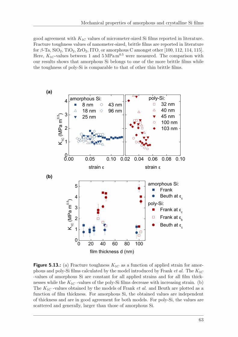
Mechanical properties of amorphous and crystalline Si films
good agreement with K1C values of micrometer-sized Si films reported in literature.Fracture toughness values of nanometer-sized, brittle films are reported in literaturefor β-Ta, SiO2, TiO2, ZrO2, ITO, or amorphous C amongst other [100, 112, 114, 115].Here, K1C-values between 1 and 5 MPa m0.5 were measured. The comparison withour results shows that amorphous Si belongs to one of the more brittle films whilethe toughness of poly-Si is comparable to that of other thin brittle films.
(a)
(b)
0.00 0.05 0.100
1
2
3
4 amorphous Si: 8 nm 43 nm 18 nm 96 nm 25 nm
K1C (
MP
a m
0.5)
strain ε
0.02 0.04 0.06 0.08 0.10
poly-Si: 32 nm 40 nm 45 nm 100 nm 103 nm
strain ε
0 20 40 60 80 1000
1
2
3
4
5 amorphous Si: Frank
Beuth at εc
poly-Si:
Frank at εc
Frank at εb
Beuth at εc
K1
C (
MP
a m
0.5)
film thickness d (nm)
Figure 5.13.: (a) Fracture toughness K1C as a function of applied strain for amor-phous and poly-Si films calculated by the model introduced by Frank et al. The K1C
-values of amorphous Si are constant for all applied strains and for all film thick-nesses while the K1C -values of the poly-Si films decrease with increasing strain. (b)The K1C -values obtained by the models of Frank et al. and Beuth are plotted as afunction of film thickness. For amorphous Si, the obtained values are independentof thickness and are in good agreement for both models. For poly-Si, the values arescattered and generally, larger than those of amorphous Si.
63

Mechanical properties of amorphous and crystalline Si films
5.4.6. Onset strain of fragmentation and delamination of Siembedded in the insulator structure
In Figure 5.14 the onset strains of fragmentation and delamination as a functionof film thickness are depicted for Si deposited onto the insulator structure and forsingle layers of ultrathin amorphous Si films, SiO2, and TiO2 films. Both, the onsetstrain of fragmentation and delamination values of SiO2 and TiO2 were taken fromliterature [100].Generally, thicker films fracture at lower strains than thinner films. Hence, the onsetstrains of fragmentation of the insulator structures are smaller than those of ultra-thin Si films. The values are similar to those of SiO2 and TiO2 with film thicknessesof the same order of magnitude. However, it is counterintuitive that the fractureresistance of the insulator structure with 5 nm Si is lower than those of the insulatorstructures with thicker capping layers. The SEM micrographs in Figure 5.15 revealthat the structures exhibit rough surfaces. This roughness might result in stressconcentrations during tensile loading and consequently, crack formation. Moreover,the Si film thickness difference between the three samples is minor compared to theoverall thickness of the structures. Hence, for the ultrathin Si films deposited on theinsulator structure no size-effect is observed.The onset strains of delamination of all films are depicted in Figure 5.14 (b). The
onset strain of delamination increases with increasing film thickness with the excep-tion of the ultrathin Si single films. As it was already the case for the onset strainof fragmentation also the onset strain of delamination of Si films deposited onto theinsulator structures are in the same order of magnitude as those of SiO2 and TiO2
with similar film thicknesses.The observed increasing onset strain of delamination as a function of film thicknessindicates that the delamination of the layer structure is buckle-limited and that the
(a) (b)
0 50 100 150 2000.05
0.10
0.15
0.20
0.25
onse
t st
rain
of
dela
min
atio
n
film thickness d (nm)
Si structure Si SiO
2
TiO2
0 50 100 150 2000.00
0.01
0.02
0.03
film thickness d (nm)
onse
t st
rain
of
fra
gm
enta
tion
Figure 5.14.: Onset strain of fragmentation (a) and onset strain of delamination (b)as a function of film thickness. For comparison also the strains of onset fragmenta-tion and delamination of single layers Si, SiO2, and TiO2 are shown. The values ofSiO2 and TiO2 were taken from literature [100].
64

Mechanical properties of amorphous and crystalline Si films
150 nm
(a) (b) (c)
Figure 5.15.: SEM micrographs of 5 nm (a), 15 nm (b) and 25 nm (c) Si depositedon the insulator structure.
adhesion of the coating to the substrate is weak. We assume that the interfacebetween Kapton® E and SiO2 fails first.
5.5. Conclusion
In situ optical microscopy, Raman spectroscopy, and resistance measurements wereused to determine the cohesive and adhesive properties of ultrathin amorphous andpoly-Si films on Kapton® E substrates. The following conclusions can be drawn:
• Amorphous Si films fracture (buckle) at lower (higher) strains compared topoly-Si films. The onset delamination of amorphous Si films can be modeledby the strain energy criterion (εsed ∝ d−0.5). The adhesion of poly-Si filmsto the substrate is very weak and buckling (εb ∝ d2) is expected as long asεsed exceeds the onset strain of buckle delamination εb. The buckle and strainenergy models result in an adhesion strength of 33 mJ/m2 for amorphous Siand a buckle width of b=840 nm for poly-Si which was confirmed by atomicforce microscopy measurements.
• The stress transfer length is proportional to the square root of the film thick-ness which indicates that the stress transfer between substrate and coating islinear elastic.
• The fracture toughness of poly-Si films is higher compared to thatof amorphous Si. The determined fracture toughness (poly-Si:K1C=3.36± 1.37 MPa m0.5; amorphous Si K1C=1.49± 0.22 MPa m0.5) areindependent of the thickness which indicates brittle fracture. The results arein good agreement with K1C -values of micrometer-sized Si films reported inliterature.
• The aluminum-induced layer exchange mechanism was applied to crystallizethe Si films and caused small Si crystallites on top of the coating and plasticdeformation of the substrate. This may lead to stress concentrations in the
65

Mechanical properties of amorphous and crystalline Si films
coating and local strain variations. Consequently, the resulting strength andtoughness values of the poly-Si films scatter but provide an indication of theorder of magnitude.
• Generally, onset fracture can be delayed by a reduction in the film thicknessand compressive residual stress, given that the adhesion is sufficient.
66
Cohesive and adhesive failure of amorphous and crystalline Ge2Sb2Te5 films
6. Cohesive and adhesive failure ofamorphous and crystallineGe2Sb2Te5 films
The cohesive properties of the phase-change material Ge2Sb2Te5 (GST) wereinvestigated. The onset strains of fragmentation of 20 nm - 400 nm thickas-deposited amorphous and crystalline GST films were determined by insitu resistance measurements, optical microscopy, and reflectance anisotropyspectroscopy (RAS) during uniaxial tensile loading. By comparing the re-sults of the applied methods RAS was introduced as a promising tool todetermine the onset strain of fragmentation of brittle films. The fracturestrength σf and fracture toughness K1C of the films were calculated. Amor-phous GST fractures at larger strains than crystalline GST. However, dueto the small Young’s modulus it is less tough than crystalline GST (amor-phous: K1C=0.4± 0.2 MPa m0.5; crystalline: K1C=0.8± 0.2 MPa m0.5).Parts of this chapter are based on a work submitted to Acta Materialia.
6.1. Introduction
Phase-change materials exhibit a prominent optical and electrical contrast betweenthe amorphous and crystalline phase and they can be reversibly and rapidly switchedbetween both phases. The reflectivity contrast [20] is exploited in rewritable opticaldata storage. The electrical resistivity changes up to several orders of magnitudeupon the phase transition [21] and offers great potential as non-volatile electronicmemory. Moreover, it has been demonstrated recently, that the phase-change ma-terial GST is a promising candidate for non-volatile display [46, 48] and data vi-sualization applications [48]. Using thin GST films in the nanometer range andtransparent conductors enable color changes upon phase change on both, rigid andflexible substrates.
Although phase-change materials have extraordinary properties some challengesstill remain. Using phase-change materials for dynamic random access memory(DRAM) for example is still demanding due to the required fast switching time andextremely high cycle numbers. The endurance of the devices is often limited by voidformation at the electrode contact due to the thickness reduction upon crystalliza-tion [28] which is 6.5 % for GST [27]. Moreover, for thin GST films the large densitychange upon crystallization leads to a pronounced mechanical stress and might re-sult in cracks in the film. Atomic force microscopy measurements of laser-inducedcrystallized GST for example show cracks in the crystalline region for laser pulses
67

Cohesive and adhesive failure of amorphous and crystalline Ge2Sb2Te5 films
in the ns-µs range [116]. Another failure mechanism which applies to display appli-cations on flexible substrates is bending or straining of the substrate which mightinduce cracks in the GST film.Consequently, it is of great interest to determine the mechanical properties of GSTfilms, especially at film thicknesses relevant for the application. In literature mostresearchers focused on the investigation of the Young’s modulus of amorphous,metastable cubic, and stable hexagonal GST. Here various methods such as wafercurvature [27], nanoindentation [117], microtensile measurements [118], and mi-cromechanical resonating beams [119] were applied. Young’s moduli between 10 GPaand 25 GPa for amorphous GST and values between 25 GPa and 60 GPa for crys-talline GST were obtained [27, 117–119] depending on the method, the film thicknessand the annealing temperature. Choi et al. [118] performed uniaxial microtensiletests of 500 nm amorphous GST and investigated the average crack spacing in thefilm as a function of strain. They determined an onset strain of fragmentation of0.6 %. However, no analysis of the crack evolution was carried out and only one filmthickness and no crystalline GST was characterized.In this chapter the cohesive and adhesive properties of amorphous and crystallineGST films in the thickness range from 20 nm to 400 nm are presented. Various insitu methods such as optical microscopy, resistance measurements, and reflectanceanisotropy spectroscopy (RAS) are applied during uniaxial loading of the samplesto determine the onset strain of fragmentation. RAS measures the difference inreflectance of linearly polarized light between two perpendicular directions (x,y) in
(a)
(b)
(c)
ϵ = 0
ϵ < ϵ on
ϵ > ϵ on
Figure 6.1.: Illustration of a thin film on a substrate applied to uniaxial tensileload. (a) No strain ε is applied and the atoms are arranged in their initial cubicstructure. (b) The film is strained and the atomic structure is distorted in tensiledirection. Brittle films exhibit only elastic deformation of the atoms while ductilematerials also show plastic deformation. (c) The strain ε exceeds the onset strain offragmentation εon and cracks are visible in the thin film. The atoms at the cracksare not bonded anymore and the stress in the film is released close to the cracks.Hence, the atomic structure starts to relax and elastic deformation of the film intensile direction decreases.
68

Cohesive and adhesive failure of amorphous and crystalline Ge2Sb2Te5 films
the surface plane [120]:∆r
r= 2 · rx − ry
rx + ry(6.1)
Note that the reflectance r is a complex number and here, we focus on the real partof the RA signal. This method is amongst others applied to monitor the growth ofsemiconductors [121], to determine the adsorption on surfaces [122], or to charac-terize the mechanical properties of a material [101, 123, 124].The latter is possible because RAS is very sensitive to small lattice parameterchanges. Uniaxial tensile strain below the onset strain of fragmentation resultsin these lattice parameter changes because the atomic structure is distorted in load-ing direction as depicted in Figure 6.1 (b). Hence, the band structure is affected andasymmetries in the reflectance of polarized light parallel and perpendicular to thestrain direction are induced. Consequently, straining of a material results in a char-acteristic RA signal. In the elastic strain regime this RA feature increases linearlywith strain till it saturates at the yield point [101, 124]. However, this method islimited to materials which show strain-induced optical anisotropy.Here, we demonstrate that RAS is additionally a promising tool to determine theonset strain of fragmentation of brittle films. As shown in Figure 6.1 (c) cracks in thefilm due to straining occur perpendicular to the loading direction and consequently,result in an anisotropy in the reflectance of polarized light parallel and orthogonalto the strain direction.Optical microscopy is additionally used to determine the onset strain of delamina-tion and to monitor the evolution of the crack patterns. That allows to calculatethe fracture strength and fracture toughness of the amorphous and the crystallineGST films.
6.2. Materials and Methods
GST films of 20 nm, 30 nm, 50 nm, 100 nm, 200 nm, and 400 nm were produced bydirect current magnetron sputtering (PVD Products) using a power of 20 W. Thebackground pressure in the chamber was better than 8 · 10−5 Pa and during thedepositions, an Ar flow of 20 sccm and a pressure of 0.67 Pa were used. In order toachieve homogeneous film thicknesses the substrate was rotated with 30 rpm. Thepolyimide substrates (Kapton® E from DuPontTM) with a thickness of 50µm werecleaned in acetone and isopropanol and baked in a furnace for at least 6 h at 200 Cprior to deposition.All GST films were amorphous as-deposited as confirmed by Raman spectroscopy.Crystallization was performed under argon atmosphere in a furnace. The sampleswere annealed at 200-210 C for 6 min with a heating rate of 30 C/min. The phasetransition to the rocksalt crystalline (fcc) phase is at around 160 C for 250 nm thickfilms for heating rates of 30 C/min [125]. XRD was carried out to analyze thecrystalline structure. A θ-2θ scan from 3 to 120 was performed with a step size of0.008.The residual stress σres of the films was determined by measuring the curvature of thepolyimide substrates with the GST films by optical microscopy and calculating σresusing Stoney’s equation [98]. For uniaxial tensile tests, the samples were mounted
69

Cohesive and adhesive failure of amorphous and crystalline Ge2Sb2Te5 films
into a tensile machine (Kammrath & Weiss GmbH). Each sample was 5 mm wideand the strain rates were 5.3·10−5 /s (optical microscopy and RAS measurement)and 1.1·10−4 /s (resistance measurements). In situ confocal light microscopy (WITecCRM200) was performed with a 100x objective to observe the crack patterns duringstepwise loading. The mean crack distance L was calculated with a Matlab routine[99]. The analysis of the crack evolution leads to fracture strength and fracturetoughness values of the GST layers.An electrical resistance module was used in a constant current mode to record thechange of the normalized resistance R/R0 of all films during uniaxial loading. Thesettings were the same as those described in Chapter 5. Due to its low specificresistance, the resistance change of amorphous GST was monitored indirectly bymeasuring the resistance of a conductive, thin Pt capping layer during loading.Hence, GST films with a 3 nm Pt capping layer were sputtered without breakingthe vacuum in between for in situ resistance measurements of amorphous GST. Adirect current power of 41 W, a pressure of 0.67 Pa, and an Ar flow of 20 sccm wereused for Pt.RAS was performed in an energy range from 1.5 to 5.5 eV in intervals of 0.02 eV andwith an integration time of 1 s per energy step. The spot size at the sample surfacewas 2 mm and the loading direction of the tensile machine was set in x-directionin Equation 6.1. The RA data was recorded during continuous loading at a singlephoton energy of the sample to track the evolution of one feature. Alternatively, datawas obtained stepwise which means a whole spectrum in the range from 1.5 to 5.5 eVwas acquired while straining was briefly interrupted. For all RAS measurements theKapton® E substrates were roughened on the back side to prevent a reflection fromthis surface.
6.3. Results
Here, first the results of a XRD measurement are introduced followed by the resid-ual stress measurements. Subsequently, the cohesive and adhesive properties of thinGST films as well as of the layer structure to tune the color appearance are pre-sented. Finally the results of the reflectance anisotropy spectroscopy of all films areintroduced.
6.3.1. Phase analysis
The Young’s modulus of hexagonal GST can be up to twice as large as that of cubicGST [119]. Hence, to choose the correct Young’s modulus of crystalline GST fromliterature it is important to know which phases are included in the annealed GSTfilms. In Figure 6.2 XRD patterns of Kapton® E with and without annealed 400 nmGST film are shown. Kapton® E exhibits broad XRD peaks which partly overlaythe XRD signals of crystalline GST. Here, the spectra are only presented up to50 as some reflections are not measurable at high angles because of the disorderedstructure. Moreover, at these high angles the peaks are difficult to distinguishbecause of their broad appearance due to small grain sizes and the high density ofpeaks.Reflections of the cubic fcc structure were clearly identifiable and a lattice constant
70

Cohesive and adhesive failure of amorphous and crystalline Ge2Sb2Te5 films
25 30 35 40 45 50
5000
10000
15000
20000 Kapton Kapton + cry. GST
hcphcp
hcpfcc
fcc
inte
nsity
(cts
.)
2θ (° )
fcc
hcp
Figure 6.2.: XRD spectra of a Kapton substrate (gray spectrum) and 400 nm crys-talline GST on Kapton (red spectrum) are presented.
of a=6.00 Awas determined which is consistent with literature [126]. These peaksare labeled in Figure 6.2. A peak fit of the hexagonal reflections was not feasibleas hexagonal and trigonal phases are not distinguishable by the angular position ofthe reflection but by the intensity. However, as the sample is texturized here, thepeak intensity does not provide information on the phase. Therefore, a quantitativeanalysis of the ratio of cubic and hexagonal phase cannot be provided.Nevertheless, the XRD spectrum indicates that both phases hcp and fcc are includedin annealed GST films. Literature values of Young’s moduli of GST strongly differ.Therefore, the inaccuracy of the Young’s modulus taken in this work does not originfrom the unknown phase-ratio but from discrepancies in literature. Won et al. [119]has demonstrated that the Young’s modulus of hexagonal GST is larger than that ofcubic GST. Here, we use a Young’s modulus of 10-20 GPa for amorphous GST andEf=30-40 GPa for crystalline GST which is consistent with literature [27, 117–119].
6.3.2. Residual stress
The determined residual stresses of all films are summarized in Table 6.1. The resid-ual stress is tensile and decreases as a function of film thickness. Crystalline GSTfilms exhibit larger residual stresses than amorphous films because of the densityincrease upon crystallization. Calculating the elastic strain values from the residualstress in the linear elastic regime yields unreasonably high values for ultrathin films
Table 6.1.: Residual stress σres of amorphous and crystalline GST of thickness d.
film thickness d (nm) σres amorphous (GPa) σres crystalline (GPa)20 0.78± 0.25 1.13± 0.3630 0.57± 0.18 0.68± 0.2050 0.30± 0.10 0.32± 0.10100 0.15± 0.05 0.16± 0.05200 0.08± 0.02 0.12± 0.04400 0.05± 0.02 0.09± 0.03
71

Cohesive and adhesive failure of amorphous and crystalline Ge2Sb2Te5 films
below 50 nm. Hence, the validation method for these ultrathin films is questionedand is not used for the calculations in the following for the thinnest layers.
6.3.3. Cohesive and adhesive properties
GST thin films
Typical crack patterns of amorphous and crystalline GST at various strain valuesare depicted in Figure 6.3. The patterns resemble those of amorphous and poly-Sipresented in Figure 5.3 in Chapter 5. Also here cracks in the crystalline film devi-ate from straight paths as they have to propagate through the grain boundaries incontrast to those in amorphous GST. Compared to the crack patterns of Si films,GST films exhibit smaller mean crack distances which indicates that the films aremore brittle. Generally, buckling was not observed for amorphous GST up to strainvalues of 20 % while crystalline films show delamination as presented in the rightmicrograph of Figure 6.3 (b).Characteristic evolutions of crack patterns are obtained upon uniaxial tensile load-ing of thin brittle films. In Figure 6.4 the mean crack distances against appliedstrain are presented for amorphous (a) and crystalline (b) thin films. Cracks inthe very thin films (20 nm and 30 nm) cannot be observed by optical microscopy, insitu AFM, and SEM measurements as the crack openings are too small. While foroptical microscopy the resolution is not sufficient, detection of the cracks by in situSEM is challenging because of charging effects of the polyimide substrate and carbonredeposition onto the film during scanning. For AFM measurements straining wasbriefly interrupted at various strain values and small areas of the film were scanned.However, as this method takes more time compared to SEM and optical microscopy
(a)
1.2% 4.0% 18.0%10 μm 10 μm 10 μm
(b)
1.2% 4.0% 18.0%10 μm 10 μm 10 μm
Figure 6.3.: (a) Exemplarily, light micrographs of crack patterns of 100 nm amor-phous GST at various strains are shown. The cracks are perpendicular to the loadingdirection and buckling is not observed. (b) Optical micrographs of crack patternsof 100 nm crystalline GST at various tensile strains are presented. In contrast toamorphous GST films, cracks do not channel through the whole film after reachingthe critical length but stop at obstacles like e.g. grain boundaries.
72

Cohesive and adhesive failure of amorphous and crystalline Ge2Sb2Te5 films
(a) (b)
0.01 0.1
crystalline:50 nm GST100 nm GST200 nm GST400 nm GST
strain ε0.01 0.1
1
10
100
1000
strain ε
m
ean c
rack
dis
tance
L (
µm
)
amorphous:50 nm GST100 nm GST200 nm GST400 nm GST
Figure 6.4.: Mean crack distance as a function of strain of (a) amorphous and (b)crystalline GST films.
measurements stress relaxation in the substrate occurs during the measurementswhich further decreases the crack openings.Generally, the onset strain of fragmentation determined by optical microscopy de-creases as a function of film thickness. Furthermore, the saturated mean crackdistance in the third regime is larger for thicker films.
Figure 6.5 shows the normalized resistance curves as a function of strain. Theonset strain of fragmentation occurs as soon as the normalized resistance R/R0
deviates from the ideal resistance change R/R0 = (1 + ε)(1 + 2νfε) (black line).In literature a 5 % deviation from the ideal behavior is often taken as a measure
0 1 2 31 . 01 . 21 . 41 . 61 . 82 . 0 ( b ) i d e a l
i d e a l + 5 % 3 n m P t
G S T : 3 0 n m 5 0 n m 1 0 0 n m 2 0 0 n m 4 0 0 n m
R/R0
s t r a i n (%)
( a )
0 1 2 3
s t r a i n (%)
Figure 6.5.: Normalized resistance plotted versus strain for (a) amorphous GSTfilms with 3 nm conductive Pt top layers and (b) crystalline GST films. The blacksolid line corresponds to the ideal resistance change while the dashed black lineshows a 5 % deviation of this ideal behavior. Exemplarily, for 100 nm crystallineGST an error bar is plotted to demonstrate scattering effects which occur betweenseveral measurements.
73

Cohesive and adhesive failure of amorphous and crystalline Ge2Sb2Te5 films
for first cracking (dashed black line) [102]. The resistance of amorphous GST,which is less conductive than crystalline GST (amorphous: (3-6)·103 Ωcm; cubic:(1-4)·10−1 Ωcm [18]), was measured indirectly by a thin Pt capping layer. To detectthe first cracks in amorphous GST the thickness of the Pt layer should neither betoo thick nor too thin. On the one hand, the first crack in amorphous GST filmswill not induce a crack in the Pt capping layer, if it is too thick. On the otherhand, very thin Pt films built islands on the GST films and consequently Pt mightinduce cracks in the GST films. The second case can be excluded by measuring theresistance change upon straining of a single Pt film. This resistance curve followsthe ideal resistance change (black line) to larger strains than all GST films as can beseen in Figure 6.5 (a). Hence, the method seems reliable. The resistance curves ofamorphous GST films dramatically increase as soon as they deviate from the idealbehavior. This indicates that a crack propagates immediately through the wholefilm as soon as it appears. For 50 nm amorphous GST the slope of the normalizedresistance is less steep. It might be that the crack opening of this thin film is toosmall to instantly induce a crack in the Pt film which propagates immediatelythrough the whole film.The normalized resistance curves of crystalline GST films (see Figure 6.5 (b))deviate from the ideal resistance change as soon as the films are strained. At lowstrains the slopes of the normalized resistance curves are the same for all crystallineGST films. This slope further increases at one strain value depending on the filmthickness. The deviation from the ideal behavior may have two possible origins:On the one hand, crystalline films may exhibit small cracks which start to openas soon as the film is loaded. At higher strain values the slope of the normalizedresistance increases due to new cracks which occur in the film. On the other hand,straining of the crystalline films may result in a piezoresistive effect.For both cases, the deviation from the initial resistance slope indicates the for-mation of first cracks such that these strain values are taken as onset strains offragmentation. For 100 nm crystalline GST scattering in data is demonstrated byan error bar which results from three different resistance measurements. Generally,the onset strain of fragmentation decreases as a function of film thickness foramorphous and crystalline GST films.
Tunable color coatingsFigure 6.6 presents optical micrographs of crack patterns of amorphous (b) and crys-talline (c) GST embedded in a tunable color coating (a) similar to that introducedin Chapter 3. The patterns differ from those of single amorphous and crystallineGST films. In contrast to single films the appearance of first individual cracks wasdifficult to observe. Instead several tiny cracks were detected at one strain valuewhich can be explained as follows: For both phases the crack openings at low strainvalues are very small such that they cannot be observed in the optical microscope.Increasing the uniaxial tensile strain causes further crack opening and several shortfractures are simultaneously visible in the optical microscope as can be seen in Fig-ure 6.6 (b) and (c) at 3.3 % strain. Upon loading the crack density increases andthe tiny cracks grow until they intersect with other cracks. At high strain valuessharp microscope images could not be taken as can be seen in Figure 6.6 (b) and(c) at 13.3 % strain. This indicates differences in height of the film which might be
74

Cohesive and adhesive failure of amorphous and crystalline Ge2Sb2Te5 films
(b)
3.3% 8.0% 13.3%10 μm 10 μm 10 μm
(c)
3.3% 8.0% 13.3%10 μm 10 μm 10 μm
(a)
5 nm Ti
150 nm Au
3 nm Ti10 nm TiN
18 nm GST
40 nm SiO2
Figure 6.6.: (a) Illustration of a tunable color coating similar to that introduced inChapter 3 is shown. Light micrographs of crack patterns of 18 nm amorphous (b)and crystalline (c) GST embedded in the tunable coating are depicted.
explained by delamination of the film.The crack distances are very narrow and the cracks are very short. Therefore, it ischallenging to determine the mean crack distance. Figure 6.7 depicts the mean crackdistance of the multilayer films for amorphous and crystalline GST as a function ofstrain. The onset strain of fragmentation is most probably overestimates as severaltiny first cracks were detected at one strain value. Nevertheless, first cracks in crys-talline GST were observed at lower strains than in amorphous GST. This trend isin good agreement with single amorphous and crystalline GST layers.
0.01 0.1
1
10
100
me
an
cra
ck d
ista
nce
L (
µm
)
strain ε
amorphous GSTcrystalline GST
Figure 6.7.: Mean crack distance as a function of applied tensile strain for amor-phous and crystalline 18 nm GST embedded in the layer structure presented inFigure 6.6 (a).
75

Cohesive and adhesive failure of amorphous and crystalline Ge2Sb2Te5 films
6.3.4. Reflectance anisotropy spectroscopy
GST thin filmsReflectance anisotropy (RAS) measurements were performed to measure the yieldpoint and onset strain of fragmentation. In Figure 6.8 a simulation of the lightpenetration depth in amorphous and crystalline GST as a function of photon energyis presented. The penetration depth describes the depth d at which the intensity ofthe light decays to 1/e of its surface value (d = λ/(4πk)). The imaginary parts of therefractive index k of amorphous and crystalline GST were taken from literature [127].Especially, for thin amorphous and crystalline GST films below 50 nm thickness thepenetration depth needs to be taken into account. For these thin films the reflectanceanisotropy spectra might origin not only from the film but also from the Kapton®
E substrate.Several representative RA spectra taken at different strains are presented in Fig-
ure 6.9. Those of amorphous GST films are shown on the left while those of crys-talline films are on the right in Figure 6.9. For comparison spectra of different filmthicknesses (30 nm, 100 nm, and 400 nm) are plotted. The solid lines represent thespectra during tensile loading and the dashed lines those during unloading of thesamples. Loading of the films results in the appearance of RA features with negativeamplitude which are called crack features in the following. For all films the positionof the crack features are marked with small black arrows in the figure. Generally,the following description of the crack features in RA are valid:
• For each film thickness the signal appears at a different photon energy whichindicates that it is not a materials property. For 100 nm amorphous GST it isfor instance at 2.8 eV while 400 nm amorphous GST shows the crack featureat approximately 2.2 eV.
• The crack feature does not appear at the beginning of straining but at a strainvalue dependent on the film thickness and phase of the sample. For 100 nmamorphous GST e.g. it occurs at approximately 1 % strain.
2 3 4 5 60
20
40
60
80
penetr
atio
n d
epth
(nm
)
photon energy (eV)
amorphous crystalline
800 600 400 200
wavelength (nm)
Figure 6.8.: Simulated light penetration depth versus photon energy of amorphousand crystalline GST.
76

Cohesive and adhesive failure of amorphous and crystalline Ge2Sb2Te5 films
620 413 310 248
−10
−5
0
Re
(∆ r
/r)
(10
−3)
0.00%0.80%2.40%2.80%4.00%4.80%6.00%6.99%6.00%4.00%2.00%
620 413 310 248
−10
−5
0
5
10
15
Re
(∆ r
/r)
(10
−3)
0.00%0.40%0.80%1.20%2.00%3.00%4.00%5.00%4.00%3.00%1.00%
−40
−30
−20
−10
0
Re
(∆ r
/r)
(10
−3)
0.00%0.40%1.00%1.20%2.00%3.00%3.99%4.99%3.99%2.00%1.00%
2 3 4 5
−30
−20
−10
0
photon energy (eV)
Re
(∆ r
/r)
(10
−3)
0.00%0.40%0.80%1.20%2.00%3.00%4.00%5.00%4.00%2.00%1.00%
2 3 4 5
−20
−10
0
photon energy (eV)
Re
(∆ r
/r)
(10
−3)
0.00%0.20%0.30%0.40%0.80%1.20%2.00%3.00%2.00%1.60%1.20%
−50
−40
−30
−20
−10
0
Re(∆
r/r
) (1
0−
3)
0.00%0.40%1.00%1.60%2.00%3.00%4.00%5.00%4.00%2.00%1.00%
(a)30 n
m G
ST
crystallineamorphous(b)
(c)
100 n
m G
ST
400 n
m G
ST
(e)
(d)
(f)
wavelength (nm) wavelength (nm)400600 300 400600 300
Figure 6.9.: RA-spectra of amorphous ((a), (c), (e)) and crystalline ((b), (d), (f))GST films at different strain values. Exemplarily, only the spectra of 30 nm ((a),(b)), 100 nm ((c), (d)), and 400 nm ((e), (f)) GST films are shown. All solid linesrepresent tensile loading and the dashed lines unloading of the sample. The RAspectra of all crystalline GST films reveal a feature at 5.06 eV. Moreover, the RAspectra of amorphous and crystalline GST films show crack features which are in-dicated by black arrows. The absolute amount of the crack feature increase as afunction of strain. Exemplarily, circles indicate the energy position of the crackfeature of 100 nm amorphous GST for different strain values.
• The crack feature has a negative amplitude and the absolute value of theamplitude increases as a function of straining. Unloading of the sample results
77

Cohesive and adhesive failure of amorphous and crystalline Ge2Sb2Te5 films
in a decrease of the absolute value of the amplitude.
• As a guide to the eye small circles in the RA spectra of 100 nm amorphous GSTrepresent the photon energy position of the feature at each strain value. Thefeature shifts to larger photon energies with increasing strain until it saturatesat 2.8 eV at approximately 2 % strain. Upon unloading the energy position ofthe feature shifts back to smaller photon energies. This shift to larger energiesupon loading and the reversible behavior upon unloading is valid for all films.
• For films thicker than 50 nm the crack feature of amorphous and crystallineGST films of the same film thickness resemble each other. The RA spectra ofamorphous and crystalline 20 nm and 30 nm films differ from each other. Thismight be due to the penetration depth of the light which is in the same orderof magnitude as the film thickness. Consequently, not only the film propertiesbut also the substrate properties are measured. The RA spectra of 20 nmamorphous GST are similar to that of the Kapton® E substrate. Hence, aninterpretation is challenging and the spectra are not included in the analysis.
In addition to the crack feature all crystalline GST films show another signal at5.06 eV. This signal grows in amplitude with increasing strain and is called elasticfeature in the following. Independent of film thickness all crystalline GST filmsshow the elastic feature at 5.06 eV which indicates that it is a material property.Moreover, also this feature is reversible and disappears upon unloading.
Tunable color coatingsFigure 6.10 shows RA spectra of amorphous (a) and crystalline (b) 18 nm thickGST films embedded in the tunable color coating. Upon uniaxial tensile loadingof the sample the whole spectrum shifts to lower intensities and several features inthe RA spectra occur. The absolute value of the pronounced feature at 1.76 eV foramorphous (2.06 eV for crystalline) GST increases as a function of strain. Unloadingof the sample results in a shift back to larger intensities. However, upon unloadingthe spectrum does not return to the initial position of the spectrum at 2 % tensilestrain.
78

Cohesive and adhesive failure of amorphous and crystalline Ge2Sb2Te5 films
(a)
2 3 4 5−60
−40
−20
0
20
photon energy (eV)
Re
(∆ r
/r)
(10
−3)
0.00%0.80%1.60%2.00%2.40%4.00%5.00%3.00%2.00%
(b)
2 4
−100
−50
0
photon energy (eV)
Re
(∆ r
/r)
(10
−3)
0.00%0.40%0.80%2.40%4.00%5.00%4.00%3.00%2.00%
300400600 300400600
3 5
wavelength (nm) wavelength (nm)
Figure 6.10.: RA spectra of amorphous (a) and crystalline (b) 18 nm GST embed-ded in the layer structure presented in Figure 6.6 (a). The spectra were taken atdifferent strain values. The solid lines represent measured spectra during tensileloading and the dashed lines those during unloading.
6.4. Discussion
6.4.1. Residual stress
The residual stresses of crystalline GST films are more tensile than those of amor-phous GST films. This trend was also observed by Pedersen et al. [27]. Theyshowed that the stress change upon crystallization is only 9 % of the theoreticallycalculated stress change which would be expected due to the large film thicknesschange upon crystallization. The observed result can be explained by a viscous flowin the amorphous phase which relieves the stress as explained by Pedersen et al.[27]. The authors show that upon annealing crystalline GST the stress relief rateis minor and cannot explain the discrepancy between measurement and calculation.Hence, they assume that the stress is relieved in the amorphous phase during growthof crystalline nuclei.The intrinsic tensile stress in the amorphous phase is formed during the fabricationprocess and might be caused by the working gas pressure during sputter deposition[128]. The thickness dependent trend of the residual stress shown here is probablyrelated to the coalescence of the islands and the atomic peening of the film duringsputter deposition [129].
6.4.2. Cohesive and adhesive properties of GST films
GST thin filmsFigure 6.11 presents the fracture strength of amorphous and crystalline GST as afunction of film thickness. The fracture strength was calculated from fragmentationkinetics in the defect-controlled regime in analogy to Chapter 5 and in analogy toliterature [107, 108]. Generally, amorphous films exhibit a smaller fracture strength
79

Cohesive and adhesive failure of amorphous and crystalline Ge2Sb2Te5 films
0 100 200 300 4000.0
0.2
0.4
0.6
0.8
1.0
fra
ctu
re s
tre
ng
th σ
f (G
Pa
)
film thickness d (nm)
amorphous fit crystalline fit
Figure 6.11.: Fracture strength values as a function of film thickness of amorphousand crystalline GST are presented. The error bars result from uncertainties of theYoung’s moduli. Fitting Griffith’s (σf ∝ d−0.5) law to the data results in bulkfracture strength values which are indicated as shaded areas.
than crystalline films. However, Figure 6.4 demonstrates that crystalline GST frac-tures at lower strains than amorphous GST. This apparent contradiction can besolved by considering that the Young’s modulus of crystalline GST (Ef=30-40 GPa[119]) is two to three times larger than that of amorphous GST (Ef=10-20 GPa[119]) which results in a higher fracture strength of crystalline GST. The film thick-ness dependence of the fracture strength can be modeled according to Griffith’s law(σf = a · d−0.5 + b). This law assumes that the dominant factor determining thefracture strength is defect growth throughout the film thickness. Thicker films resultin smaller fracture strength values because a larger film volume exhibits a highernumber of volume defects. Consequently, the probability of critical defects at acertain stress is larger for thicker films. However, the fracture strength convergesagainst a bulk fracture strength value which corresponds to the fit parameter b andis plotted as shaded areas in Figure 6.11. The fitparameter a includes the fracturetoughness K1C and an unknown geometry factor.In Figure 6.12 (a) the fracture toughness values of amorphous and crystalline GST
are shown as a function of strain. These values were evaluated by an energy-basedapproach in analogy to Chapter 5. A two-dimensional shear lag model derived byFrank et al. [30] was used to derivate the fracture toughness. The model is valid inthe strain regime εc < ε < εb, with εc the crossover strain where the stress relaxationzones start to overlap and εb the onset strain of delamination. For amorphous GSTthe model is applied in the strain regime εc < ε < εsat as at larger strains no furthercracks occur. To calculate the fracture toughness, first the stress transfer lengthξ = Lc/2 needs to be identified. As the decrease in onset strain of fragmentationas function of strain is low (see Figure 6.4) it is challenging to determine Lc. Con-sequently, in contrast to Si the critical length Lc was determined from the meancrack distance at saturation Lc = 1.5 · Lsat [107]. At low strains K1C increases as afunction of strain which is expected as first cracks occur at the largest defects andconsequently result in a reduced effective fracture toughness. The fracture toughness
80

Cohesive and adhesive failure of amorphous and crystalline Ge2Sb2Te5 films
(a)
(b)
0 2 4 6 8 10 120.0
0.5
1.0
1.5amorphous:
50 nm 100 nm 200 nm 400 nm
crystalline: 50 nm 100 nm 200 nm 400 nm
K1
C (
MP
a m
0.5)
strain ε (%)
0 100 200 300 4000.0
0.5
1.0
1.5
K1
C (
MP
a m
0.5)
film thickness d (nm)
amorphous: Beuth
Frank at εc
Frank at εb
crystalline: Beuth
Frank at εc
Frank at εb
Figure 6.12.: (a) Fracture toughness K1C plotted as function of strain for amor-phous and crystalline GST determined by the model introduced by Frank et al. (b)The K1C-values obtained by the model of Frank et al. and Beuth are plotted as afunction of film thickness. Generally, crystalline GST is tougher than amorphousGST.
saturates at higher strain values as soon as the stress in the film reaches the fracturestrength of the film. Exemplarily, for each film thickness one error bar is plottedwhich result from uncertainties of the Young’s moduli. Compared to these uncer-tainties, a variation in Lc has a minor influence on the calculated fracture toughnessbut changes the evolution of the fracture toughness as a function of strain.In Figure 6.12 (b) the K1C-values obtained at εc and εb, or respectively εsat for the
model of Frank et al. are compared to the values calculated with the model of Beuth[111]. This model relies on linear elastic response of substrate and coating and theresidual stress of the film was considered in the calculated K1C values. For bothmodels the obtained values scatter but are independent of the film thickness whichindicates that there is no plastic deformation in the films. For amorphous GST anaverage fracture toughness of K1C=0.4± 0.2 MPa m0.5 is obtained and for crystallineGST the value is K1C=0.8± 0.2 MPa m0.5. Compared to other thin brittle films withK1C values around 1-5 MPa m0.5 [30, 85] these values are small. The difference in
81
Cohesive and adhesive failure of amorphous and crystalline Ge2Sb2Te5 films
K1C values can be explained by the small Young’s modulus of GST compared toother brittle materials.Polymers also exhibit a small Young’s modulus and a reduced fracture tough-ness, but they are still used as substrate material for flexible electronics. Con-sequently, in some applications the criteria of maximum strain to fracture (εon ∝K1C/Ef ) and the energy release rate which is the maximum stored energy (K2
1C/Ef )are more important. For flexible electronics e.g. the strain to fracture valueis more important as it describes the failure of the device. Comparing thestrain to fracture values of GST (amorphous GST: K1C/Ef=(30± 15)·10−6 m0.5;crystalline GST: K1C/Ef=(23± 6)·10−6 m0.5) with those of Si (amorphous Si:K1C/Ef=(18± 3)·10−6 m0.5; crystalline Si: K1C/Ef=(20± 8)·10−6 m0.5) shows thatthe values are comparable.
6.4.3. Onset strain of fragmentation and delamination of GSTfilms
In this subsection first the reflectance anisotropy measurements are presentedbecause they help to understand the anomaly in resistance measurements of thecrystalline GST films. Subsequently, these results are compared to the onset strainsof fragmentation determined by optical microscopy and resistance measurements.Finally, the onset strain of delamination is shown.The onset strains of fragmentation of amorphous GST were obtained from RAspectra at the strain value where the crack feature starts to grow. Figure 6.13 (a)presents the intensity value of Re(∆r/r) at the respective energy value of the crackfeature as a function of strain. The films of all thicknesses first possess the samelinear change of the anisotropy signal behavior during loading. The strain valuewhere the RA signal deviates from the linear behavior depends on the film thicknessand is taken as onset strain of fragmentation. Thicker films start to deviate atlower strain values from the initial linear behavior than thinner films.
The origin of this deviation can be explained as follows: Crack formation in thefilm always appears perpendicular to the loading direction. Hence, an anisotropy inthe reflectance of the linearly polarized light between two perpendicular directionsis induced. With increasing strain more and more cracks form, the anisotropyaugments, and the intensity of the crack feature increases. A mean crack distanceof 970 nm obtained from Figure 6.4 and a crack opening of 80 nm determined by insitu atomic force microscopy measurements were used to simulate the behavior oflinear polarized light at the cracks.Figure 6.14 shows the electromagnetic response of a 100 nm amorphous GST slitarray with a period of 970 nm to an incident transverse magnetic plane wave. Theelectromagnetic response has been modelled using the finite-element modellingsoftware COMSOL Multiphysics. The surface plot shows the x-component of theelectric field and the arrows indicate the relative electric field. This image canbe seen as snapshot where incoming and reflected light interfere. The incidentlight couples to surface plasmon polaritons (SPP) at the upper (air/GST) andlower (GST/Kapton® E) surface which is enabled by the fundamental mode ofthe slit array [130]. Due to the significantly altered SPP dispersion relation atthe GST/Kapton® E interface the coupling between the SPP modes of the upper
82

Cohesive and adhesive failure of amorphous and crystalline Ge2Sb2Te5 films
(a)
-0.04
-0.03
-0.02
-0.01
0.00stepwise:
30 nm 50 nm 100 nm 200 nm 400 nm
Re(∆
r/r)
at E
E=4.22 eVE=4.00eVE=2.80 eVE=3.80 eVE=2.22 eV
(b)
0 1 2 3 4 5-0.010
-0.005
0.000
0.005
0.010
0.015 continuously: 20 nm 30 nm 50 nm 100 nm 200 nm 400 nm
Re(∆
r/r)
at 5
.06
eV
strain ε (%)
Figure 6.13.: Evolution of the RA signals of amorphous (a) and crystalline (b) GSTfilms as a function of strain. The data in (a) were obtained from RA spectra at oneenergy per thickness. For crystalline GST (b) the values were measured continuouslyat 5.06 eV.
and lower surface can be considered weak. In analogy to transmissive gratings theoverall electromagnetical response depends in general on the geometrical parametersof the slit array. Here, the crack distance (L > λ) and crack opening (a < λ) areconstant and the film thickness acts as critical coupling parameter.
Figure 6.15 compares the measured and simulated RA spectra of 50 nm, 100 nm,and 400 nm amorphous GST. The spectral position of the crack feature is in goodagreement for measurement and simulation. With increasing film thickness the crackfeature shifts to smaller photon energies. However, the exact shape of the spectradiffer for measurement and simulation. The simulation assumes a perfect periodicgrating but in reality crack openings and crack distances vary. Consequently, themeasurement averages grating structures with slightly different periodicity whichexplains why the spectra are smoother than those of the simulations. Moreover, forthe simulation we assume that the cracks are perfectly oriented to the polarizationof the light. During the measurement a deviation of some degrees may easily occurwhich might also influence the RA spectra.
83

Cohesive and adhesive failure of amorphous and crystalline Ge2Sb2Te5 films
4x 10
1
0.5
0
-0.5
-1 ele
ctric
field
, x-
com
ponent (V
/m)
x
y
100 nmair GST Kapton
z
Figure 6.14.: Simulation of an incident transverse magnetic field at Ephoton=2.70 eV(λ= 460 nm) on a 100 nm amorphous GST slit-array with period L=970 nm and slitwidth a=80 nm. The surface plot indicates the x-component of the electric field andthe arrows present the relative electric field.
The reflectance anisotropy of crystalline GST was recorded at a photon energy of5.06 eV during continuous loading (see Figure 6.13 (b)). At low strains the films ofall thicknesses exhibit a linear increase in intensity as a function of strain, which isperfectly reversible upon cyclic loading. The strain value where the signal starts to
(a) (b)
2 3 4 5-120
-80
-40
0amorphous:
50 nm 100 nm 400 nm
Re
(∆r/
r) (
10
-3)
photon energy (eV)
600 300
wavelength (nm)
2 3 4 5-50
-40
-30
-20
-10
0
10
Re(∆
r/r)
(10
-3)
photon energy (eV)
600 300
wavelength (nm)
Figure 6.15.: Measurement (a) and COMSOL simulation (b) of RA spectra of50 nm, 100 nm, and 400 nm amorphous GST films. The thickness-dependent trendof the spectral position of the crack feature is identical for measurement and sim-ulation. For the simulation crack openings of 80 nm and crack distances of 970 nmwere assumed. The measured spectra were recorded at approximately 5 % strain.
84

Cohesive and adhesive failure of amorphous and crystalline Ge2Sb2Te5 films
deviate from this linear behavior differs for each film thickness. It is taken as yieldpoint where the elastic deformation stops. Here, the change of the RA spectra atstrains larger than the yield point is difficult to interpret as the crack feature mightinfluence the signal. Generally, a saturation of the RA signal corresponds to plasticdeformation [101] and a decrease of the signal results from relaxation of the filmdue to crack formation. Here, the decrease of the RA signal is not only caused bystress relaxation but also by the overlying crack feature signal.The RA feature at 5.06 eV can be attributed to the piezo-optic tensor and reflectcritical points in the electronic band structure of metastable cubic GST. Theelectronic band structure of cubic GST was calculated in literature [53]. It is verycomplex and the authors were not able to determine all critical points. Moreover,the results are based on calculations for the lowest energy structure where intrinsicvacancies are ordered. At real conditions they are randomly distributed in thematerial. Consequently, it is challenging to find a transition in the band structurewhich corresponds to the RA feature at 5.06 eV. However, numerous conductivebands around 5 eV [53] at the Γ-point and a high density of states at this energy[131] indicate that several transitions may be accessible. That would also explainthat the RA signal at 5.06 eV is much broader than usually observed for a singletransition [101].
To demonstrate that the strain where the reflectance anisotropy features appearcan be attributed to the onset strain of fragmentation we compare these strainvalues with the onset strain of fragmentation determined by optical microscopy andresistance measurements. Figure 6.16 (a) presents the onset strains of fragmentationof amorphous GST and Figure 6.16 (b) those of crystalline GST films. The valuesobtained by RAS are in excellent agreement with those of the two other methods.This indicates that the method is reliable. Moreover, optical microscopy and
(a) (b)
0 100 200 300 4000
1
2
3
4RAS
stepwise
microscopyresistance
onse
t st
rain
of fr
agm
enta
tion (
%)
film thickness d (nm)
0 100 200 300 400
microscopy RAS at 5.06 eV:resistance stepwise
continuously
film thickness d (nm)
Figure 6.16.: Thickness-dependent onset strain of fragmentation of amorphous (a)and crystalline (b) GST films determined by RAS, optical microscopy, and resistancemeasurements. Here, continuously means that the RA data were recorded duringcontinuous loading at a single photon energy. Stepwise means that a whole spectrumwas acquired while the straining was briefly interrupted.
85
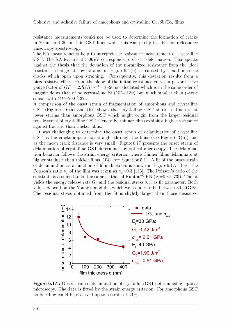
Cohesive and adhesive failure of amorphous and crystalline Ge2Sb2Te5 films
resistance measurements could not be used to determine the formation of cracksin 20 nm and 30 nm thin GST films while this was partly feasible for reflectanceanisotropy spectroscopy.The RA measurements help to interpret the resistance measurement of crystallineGST. The RA feature at 5.06 eV corresponds to elastic deformation. This speaksagainst the thesis that the deviation of the normalized resistance from the idealresistance change at low strains in Figure 6.5 (b) is caused by small intrinsiccracks which open upon straining. Consequently, this deviation results from apiezoresistive effect. From the slope of the initial resistance curves a piezoresistivegauge factor of GF = ∆R/R · ε−1=10-20 is calculated which is in the same order ofmagnitude as that of polycrystalline Si (GF=±30) but much smaller than p-typesilicon with GF=200 [132].A comparison of the onset strain of fragmentation of amorphous and crystallineGST (Figure 6.16 (a) and (b)) shows that crystalline GST starts to fracture atlower strains than amorphous GST which might origin from the larger residualtensile stress of crystalline GST. Generally, thinner films exhibit a higher resistanceagainst fracture than thicker films.
It was challenging to determine the onset strain of delamination of crystallineGST as the cracks appear not straight through the films (see Figure 6.3 (b)) andas the mean crack distance is very small. Figure 6.17 presents the onset strain ofdelamination of crystalline GST determined by optical microscopy. The delamina-tion behavior follows the strain energy criterion where thinner films delaminate athigher strains ε than thicker films [104] (see Equation 5.1). A fit of the onset strainof delamination as a function of film thickness is shown in Figure 6.17. Here, thePoisson’s ratio νf of the film was taken as νf=0.3 [133]. The Poisson’s ratio of thesubstrate is assumed to be the same as that of Kapton® HN (νs=0.34 [73]). The fityields the energy release rate G0 and the residual stress σres as fit parameter. Bothvalues depend on the Young’s modulus which we assume to be between 30-40 GPa.The residual stress obtained from the fit is slightly larger than those measured
0 100 200 300 4000
2
4
6
8
10
12
14 data
fit G0 and σ
res
onset st
rain
of de
lam
ination
(%
)
film thickness d (nm)
Ef=30 GPa:
G0=1.42 J/m
2
σres
= 0.61 GPa
Ef=40 GPa:
G0=1.90 J/m
2
σres
= 0.81 GPa
Figure 6.17.: Onset strain of delamination of crystalline GST determined by opticalmicroscopy. The data is fitted by the strain energy criterion. For amorphous GSTno buckling could be observed up to a strain of 20 %.
86

Cohesive and adhesive failure of amorphous and crystalline Ge2Sb2Te5 films
by substrate curvature. This indicates either that the residual stress determinedexperimentally is underestimated or that the Young’s modulus of crystalline GSTtaken from literature is overestimated. The determined energy release rate is inthe same order of magnitude as that of typical surface energies such as of Si [134].Amorphous GST does not exhibit any buckling up to a strain of 20 %.
Tunable color coatingsFigure 6.18 presents the evaluation of the RA spectra shown in Figure 6.10. In
analogy to amorphous single GST films also here, the intensity values Re(∆r/r)of RA features as a function of strain are shown. For amorphous and crystallinefilms respectively, two features were analyzed. The onset strain of fragmentationwhich is the strain value where the signal deviates from the initial linear behavioris not as obvious as those of single amorphous GST films (see Figure 6.13 (a)). Thiscan be explained as follows: First cracks of these layered structures do not channelthrough the whole film as soon as they reach their critical length. Instead they arevery short (see Figure 6.6) and hence, do not cause a large anisotropy in the spectra.However, for both, amorphous and crystalline GST films embedded in the tunablecolor coatings the evaluated onset strains of fragmentation of both crack featuresyield the same value. The onset strain of fragmentation of amorphous GST is atε=2.4 % and that of crystalline GST is at ε=1.6 %.The onset strain of fragmentation determined by RAS and optical microscopy arecompared in Figure 6.19. Generally, the strain at onset fragmentation measured byoptical microscopy is lower than that measured by RAS which might be explainedby the first small cracks in the film which do not cause a large anisotropy. However,for both methods the same trend is observed. The color coating that includes crys-talline GST cracks at lower strains than that with amorphous GST. This trend was
0 . 0 0 0 . 0 1 0 . 0 2 0 . 0 3 0 . 0 4 0 . 0 5- 0 . 1 5
- 0 . 1 0
- 0 . 0 5
0 . 0 0
a m o r p h o u s : E = 1 . 7 6 e V E = 3 . 8 8 e V
c r y s t a l l i n e : E = 2 . 0 6 e V E = 3 . 4 6 e V
Re(∆r
/r)
s t r a i n ε
Figure 6.18.: Evolution of the RA signals of amorphous (blue graphs) and crys-talline (orange and red graphs) GST embedded in the layer structure. The Re(∆r/r)value was recorded at two photon energies for amorphous and crystalline GST re-spectively as the spectra exhibit two features at different photon energies (see Fig-ure 6.10).
87

Cohesive and adhesive failure of amorphous and crystalline Ge2Sb2Te5 films
-0.5
0.0
0.5
1.0
1.5
2.0
2.5
on
se
t st
rain
of
fra
gm
en
tatio
n (
%)
amorphous
RAS microscope
crystalline
Figure 6.19.: Onset strain of fragmentation of amorphous and crystalline GST em-bedded in the tunable color coating determined by optical microscopy and RAS.
also detected for single amorphous and crystalline GST films. Both color coatingsfracture at lower strains than single GST layers.
6.5. Conclusion
In conclusion we have investigated the cohesive and adhesive properties of amor-phous and crystalline GST films in the film thickness range from 20 nm to 400 nmby uniaxial tensile tests. Different in situ methods such as optical microscopy, re-sistance measurements, and reflectance anisotropy spectroscopy were applied.
• Generally, thinner films start to fracture at higher strains than thicker filmsdue to a size effect in fracture strength. Amorphous films exhibit a higheronset strain of fragmentation than crystalline films. Nevertheless, amorphoussamples show a lower fracture strength and fracture toughness than crystallinefilms. This is due to the small Young’s modulus of amorphous GST. Also crys-talline GST has a small Young’s modulus compared to other brittle materialssuch as Si or Ta. This explains why the fracture toughness values of GST(amorphous: K1C=0.4± 0.2 MPa m0.5; crystalline: K1C=0.8± 0.2 MPa m0.5)are smaller compared to those of other brittle films. However, the maximumstrain to fracture of GST is similar to that of Si.
• The adhesion of amorphous GST films to Kapton® E is good and the films donot delaminate up to a strain of 20 %. Crystalline GST starts to delaminateat lower strains and the film thickness dependence of the delamination followsthe strain energy criterion.
• It was demonstrated that RAS is a reliable tool to determine the onset strainof fragmentation. This method is even feasible for very thin films where op-tical microscopy, atomic force microscopy, and scanning electron microscopyare limited because of the small crack openings of the films. Note that thesensitivity of RAS as onset strain of fragmentation detector strongly depends
88

Cohesive and adhesive failure of amorphous and crystalline Ge2Sb2Te5 films
on the crack pattern. Short cracks were first detected by optical microscopycompared to RAS. This was demonstrated for the tunable color coatings.
• The appearance of an elastic feature of crystalline GST proves that the phasetransition from amorphous to crystalline does not cause intrinsic cracks inthe film but that first cracks occur upon loading. Moreover, the RA signaldecreases at strains larger than the yield point strain because crack formationresults in relaxation of the atomic structure.
• Resistance measurements of crystalline GST show a piezoresistive effect whichis in the same order of magnitude as that of polycrystalline Si.
89


General discussion
7. General discussion
The aim of this thesis is to lay the materials foundations to develop newconcepts for static and tunable color devices which are described in the pre-vious chapters. In contrast, this chapter focuses on possible applications ofthe introduced color coatings. In the first part the long-term color stabil-ity of static and tunable color coatings is investigated. In the second partthe switching speed, endurance, and resolution of phase-change materialsare compared to existing display technologies. Moreover, the influence ofmechanical properties on possible applications is discussed. Note that thepresented color coatings are prototypes and here we discuss which propertiesneed to be improved for future applications.
7.1. Long-term color stability
7.1.1. Static color coatings
In Chapter 2, three different color coatings based on metal, insulator, and semi-conductor layers as underlying substrate materials were developed. For the applica-tion as decorative coatings, solar cells, or photodetectors, it is of great importancethat the absorption resonance remains stable for at least several years. A shift ofthe depth or spectral position of the absorption resonance affects the Lab valueswhich were calculated from the reflectance spectra. Hence, we compare the colorappearance of the coatings 2.5 years after deposition with the color measurementsperformed directly after fabrication.Figure 7.1 presents photographs of the three different sample structures on a smoothand rough substrate taken 2.5 years after fabrication. Compared to the color appear-ance of the structures shown in Figure 2.2, the appearance of the metal structurehas changed completely. The sample surfaces exhibit inhomogeneous color appear-ances. Spots which deviate from the initial colors are visible which occur especiallyat the edge of the samples. This indicates that gold has diffused into the thin amor-phous Si capping layer. Transition metals undergo direct interstitial diffusion inamorphous Si. Au diffuses faster in amorphous Si than in crystalline Si, becausein the latter Au atoms are temporary trapped at intrinsic defects which is not thecase for amorphous Si [135]. The diffusion coefficient of Au in amorphous Si wasmeasured between 400 C and 800 C and exhibits an Arrhenius-like behavior withan activation energy of 1.5 eV [136]. Extrapolating the diffusion coefficient at roomtemperature (21 C) from this data results in a value of 6.39·10−30 cm2/s. Thisvalue is small compared to the diffusion coefficient D of Au in amorphous Ge atroom temperature (D=5.91·10−18 cm2/s [137]). Nevertheless, for long-term stabilityof the color appearance a diffusion barrier between Si and Au or a replacement of Au
91
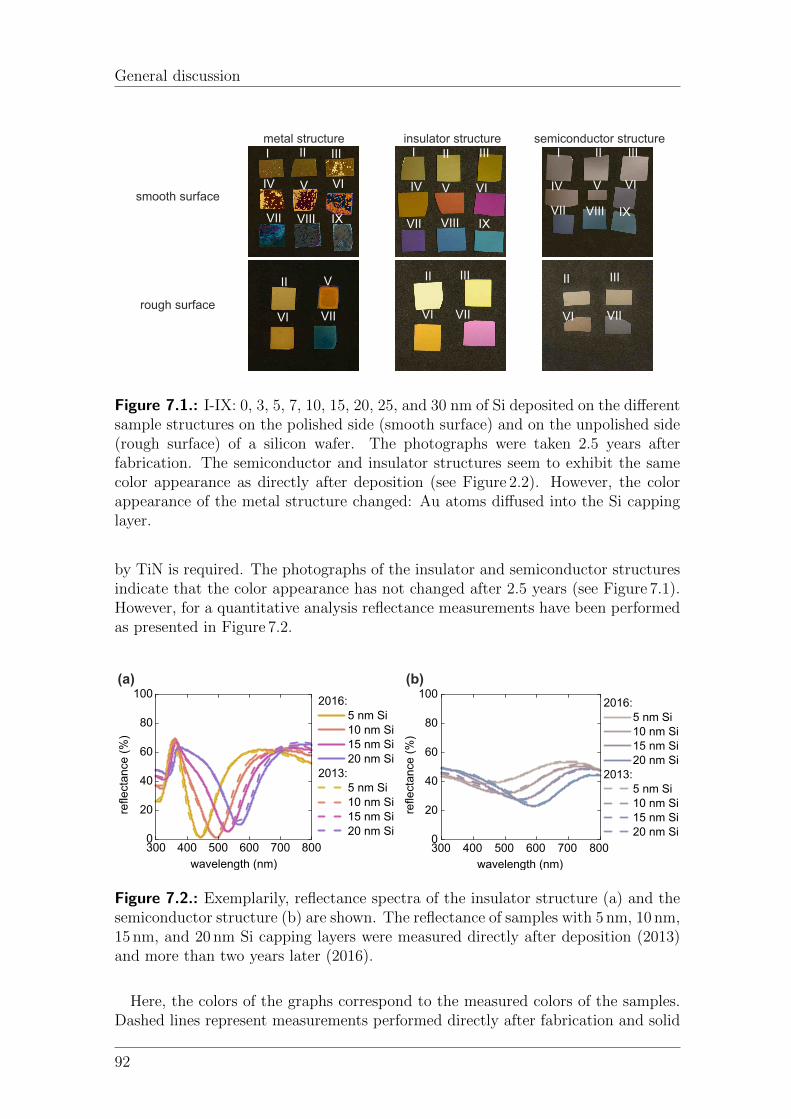
General discussion
smooth surface
rough surface
I II III
IV V VI
VII VIII IX
II V
VI VII
I III IIIII III
IVIV V VVI VI
VIIVII VIII
VIIIIX
IX
II II
VI VIVII VII
III III
metal structure insulator structure semiconductor structure
Figure 7.1.: I-IX: 0, 3, 5, 7, 10, 15, 20, 25, and 30 nm of Si deposited on the differentsample structures on the polished side (smooth surface) and on the unpolished side(rough surface) of a silicon wafer. The photographs were taken 2.5 years afterfabrication. The semiconductor and insulator structures seem to exhibit the samecolor appearance as directly after deposition (see Figure 2.2). However, the colorappearance of the metal structure changed: Au atoms diffused into the Si cappinglayer.
by TiN is required. The photographs of the insulator and semiconductor structuresindicate that the color appearance has not changed after 2.5 years (see Figure 7.1).However, for a quantitative analysis reflectance measurements have been performedas presented in Figure 7.2.
(a) (b)
300 400 500 600 700 8000
20
40
60
80
100
refle
ctance
(%
)
wavelength (nm)
2016: 5 nm Si 10 nm Si 15 nm Si 20 nm Si
2013: 5 nm Si 10 nm Si 15 nm Si 20 nm Si
300 400 500 600 700 8000
20
40
60
80
100
refle
cta
nce
(%
)
wavelength (nm)
2016: 5 nm Si 10 nm Si 15 nm Si 20 nm Si
2013: 5 nm Si 10 nm Si 15 nm Si 20 nm Si
Figure 7.2.: Exemplarily, reflectance spectra of the insulator structure (a) and thesemiconductor structure (b) are shown. The reflectance of samples with 5 nm, 10 nm,15 nm, and 20 nm Si capping layers were measured directly after deposition (2013)and more than two years later (2016).
Here, the colors of the graphs correspond to the measured colors of the samples.Dashed lines represent measurements performed directly after fabrication and solid
92

General discussion
Table 7.1.: Color difference ∆E of the insulator and semiconductor structure di-rectly after deposition (2013) and 2.5 years later (2016).
Insulator structure Semiconductor structureSi thickness (nm) ∆E Si thickness (nm) ∆E
0 5.73 0 0.983 2.86 3 0.595 2.44 5 0.627 5.42 7 0.6810 9.69 10 1.0115 7.11 15 1.3420 4.61 20 1.1225 6.40 25 1.0830 3.88 30 1.13
lines those determined 2.5 years after deposition. Generally, the spectra are shiftedto lower reflectance compared to the measurements performed directly after deposi-tion. Moreover, the spectral position of the absorption resonance slightly shifted tolonger wavelengths for the insulator structure (a) and semiconductor structure (b).To evaluate the color change over time the color difference ∆E between the colorappearance directly after deposition and 2.5 years later was calculated as presentedin Table 7.1. The insulator structure exhibits considerably larger ∆E values thanthe semiconductor structure. Here, a shift of the absorption resonance to differentwavelengths has a larger influence on the color appearance as the resonances arenarrower.Several measurements of the same sample with the photospectrometer resulted indeviations of ∆E=1.21± 0.85. This value was derived from both measurements atdifferent parts of the sample, and measurements which were each performed aftera new calibration of the photospectrometer. The deviations of the colors of thesemiconductor structure measured 2013 and 2016 are smaller than this error. Con-sequently, this structure has not significantly changed its color. However, the ∆Evalues determined for the insulator structure cannot be explained from the inaccu-racy of the instrument. The color tolerances in industry depend on the application:In the automotive industry parts with ∆E values below 1.4 are automatically deliv-ered while values below 1.7 need further consideration [138]. In commercial repro-duction on printing presses color reproduction is not as strict as that in automotiveindustry. Here, ∆E between 3 and 6 are accepted [139]. In average, the color changeof the insulator structure is below ∆E=6, but it should be improved in the futureby replacing the materials.The results presented here give a hint on the color stability of the three differentstatic color coatings. However, more testing methods depending on the applicationof the coating should be performed to verify the long-term color stability. Pos-sible methods are e.g. annealing or cooling cycles to determine the temperature-dependent color stability.
93

General discussion
7.1.2. Tunable color coatings
GST and Si films embedded in the coatings introduced in Chapter 3 change colorupon amorphization or crystallization. The corresponding ∆E value is large (GST:∆E=25.45; Si: ∆E=47.18) and proves that a different color is observed upon phase-change for both systems. These samples were fabricated in April and May 2014 andthe color stability of the coatings was evaluated 2 years later in April 2016.Figure 7.3 depicts reflectance spectra of amorphous and crystalline layer structuresmeasured directly after deposition (2014) and two years later (2016). The colors ofthe graphs corresponds to the measured colors of the samples. For both materials,GST (a) and Si (b), the deviations of the reflectance spectra recorded at differentdates are marginal. Table 7.2 presents ∆E values calculated from the reflectancespectra shown in Figure 7.3. The amorphous and crystalline layered structures basedon GST exhibit a long-term color stability as the ∆E values are on the same or-der of magnitude as the inaccuracy of the photospectrometer. This proves that athin Ti-TiN diffusion barrier, which was deposited between Au and GST, preventsinterdiffusion and guarantees a better long-term stability. The color difference ofthe tunable color coating based on Si is a bit larger than the inaccuracy of thephotospectrometer. Especially, the crystalline sample exhibits a pronounced colorchange which is caused by diffusion. The sample was annealed to 800 C to crys-tallize Si and at this temperature diffusivities of the embedded materials are large.The microscope image in Figure 3.9 (a) exhibits small dots inside and outside thelaser-amorphized region which might be caused by diffusion. As these dots are notobserved for the as-deposited film (see Figure 3.9 (b)) it can be assumed that theyare induced by annealing. Hence, the annealed crystallized sample is more suscep-tible to interdiffusion which results in a more pronounced color change. However,the color difference of the graphs of the crystalline Si structures in Figure 7.3 (b) isdifficult to observe by human eye although the ∆E value exceeds one.The color difference between the amorphous and crystalline phase of the color coat-ing is still pronounced 2 years after deposition: ∆E=40.42 for the Si color coating
(a)
300 400 500 600 700 8000
20
40
60
80
100
reflecta
nce (
%)
wavelength (nm)
2016: as-dep. GST cry. GST2014: as-dep. GST cry. GST
(b)
300 400 500 600 700 800
wavelength (nm)
2016: as-dep. Si cry. Si 2014: as-dep. Si cry. Si
Figure 7.3.: Measured reflectance spectra of the tunable color coatings based onGST (a) and Si (b) are presented. The spectra determined directly after deposition(2014) and 2 years later (2016) do not deviate from each other.
94

General discussion
Table 7.2.: Color difference ∆E of the tunable color coatings based on Si and GSTdirectly after deposition (2014) and 2 years later (2016).
GST Siphase ∆E phase ∆E
amorphous 1.69 amorphous 2.91crystalline 1.48 crystalline 4.15
and ∆E=25.47 for the tunable GST coating.
7.2. Application of the tunable color coating
7.2.1. Introduction
Display technologies can be divided into two types based on differences in theirlight source: Active lighting displays include emissive and transmissive modes andpassive lighting displays work in reflectance. The latter are superior for outdoor ap-plications and provide excellent readability under sunlight. Moreover, compared toactive lighting displays the energy consumption is reduced as images are displayedby reflecting the light. Paper-like display technologies which have already been com-mercialized have the drawback that the low switching time makes them unfeasiblefor video content. However, new technologies with high potential for the applicationin mobile electronic devices have been developed. It is assumed that the market forelectronic papers increases by a compound annual growth rate of 16.4 % during theperiod 2015 to 2020 [140].The color coatings based on ultrathin semiconductors introduced in this work areprototype devices. As they work in reflectance and have a low power consumptiondue to their stable color appearance they are potential future candidates for reflec-tive display technologies.In this chapter we investigate possibly necessary improvements of tunable color coat-ings based on ultrathin phase-change materials by comparing them to the propertiesof existing electronic papers. Here, the focus is on resolution, power consumption,switching speed, cycling numbers, and mechanical properties. Therefore, first ashort overview of various electronic paper technologies is given [141, 142].Electrophoretic displays: Positively charged black particles and negatively chargedwhite particles can be positioned vertically by applying a controlled electric field. Adesired gray scale can be obtained by manipulating the electrical field properly. Thisdisplay technology based on bistability is heavily employed in e-Reader applications.Colors of the display are not ideally realized by a color filter because the brightnessis reduced. The drawback of this technology is the low switching time and the dif-ficulty to display a desired gray scale by simple and short drive waveforms. Besidesvertical electrophoretic displays also horizontal electrophoretic displays exist. Here,homogeneously distributed particles in a pixel absorb light and produce a dark state.Light is transmitted through the pixel onto a reflector in the light state where allparticles are collected into a laterally small area. Moreover, a hybrid vertical andhorizontal electrophoretic technology was realized which is called electrokinetic and
95

General discussion
has higher switching speeds. Electronic papers based on electrophoretic displays areheavily applied e.g. in Amazon’s kindle.Electrofluidic displays: These displays contain colored oil which is confined insidethe pixel. Above the oil film the pixel is filled with water and below a fluoropolymercoating exists on top of a lower transparent electrode and a white reflective substrate.A thin oil film is formed on the fluoropolymer coating because the fluoropolymer ishydrophobic. Applying a voltage between water and electrode results in a polarizedwater/fluoropolymer interface. Hence, the polymer is water wettable and the oilfilm is pushed to the side. This effect strongly depends on the voltage and a largervoltage yields a smaller area which is covered by the oil. The switching speed ofthese displays exceeds those of electrophoretic displays and the power consumptionis low as no backlight is required. However, the display is not bistable. Electrofluidicdisplays are developed and produced by the company Gamma Dynamics.Microelectromechanical systems (MEMS): MEMS are used to modulate light bychanging the length of an optical cavity. A deforming membrane which changes thecavity length and a film stack that defines the color appearance are implemented inthe device. In the open state light is reflected in a specified wavelength range anda color is visible. In the collapsed state the gap between membrane and film stackis closed and only UV light reflection occurs. The color states are defined by RGBareas. The disadvantage of this technology is the complex fabrication for large scalemodules and the limited viewing angle. The company Qualcomm commercializedthe MEMS display Mirasol.Electrochromic displays: These displays are based on materials which reversiblychange color when a voltage is applied. There is a large variety of chemistry, per-formance, and construction of display devices based on electrochromic materials.Generally, electrochromic materials are placed on patterned transparent electrodeswhich work as pixels. The fabrication is cheap and the driving voltage to tune thecolor is low. However, the durability and speed are low. In the past these displayswere e.g. applied as smart Valentines gift card sold by Marks & Spencer in the UK[143].Photonic crystals: The propagation of electromagnetic light interacts with the spac-ing of periodic nanostructures and results in selective transmission or reflection ofthe light. Tuning the spacing of the structure changes the color appearance of thephotonic crystal. Two displays based on photonic structures are in development.Systems that control the interspacing of metal nanoparticles in electrophoretic col-loidal suspension by applying a voltage are developed by the company Nanobrick.The company Opalux fabricates an expandable electroactive polymer which includessilica beads. Both systems are not commercialized as some challenges still remain.Currently, only unit pixels or simple segments are fabricated but matrix addressingstill needs to be demonstrated. Hence, white color is difficult to create as it requiresRGB pixels.
7.2.2. Resolution
Nowadays, displays of mobile devices exhibit vivid colors and high resolutions. TheiPhone 6s Plus has e.g. a resolution of 401 ppi (pixels per inch) [144] while theGalaxy S6 and S6 edge from Samsung are equipped with a display that has 577 ppi
96
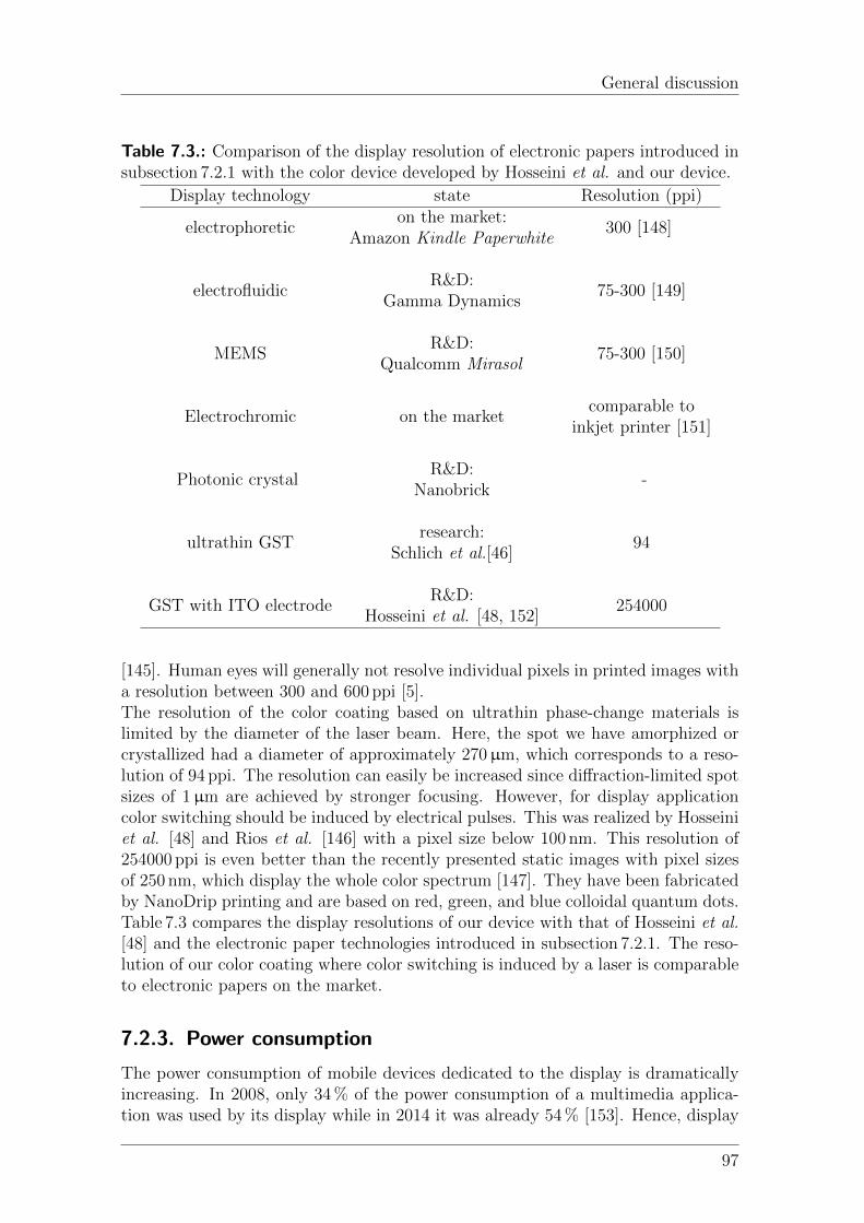
General discussion
Table 7.3.: Comparison of the display resolution of electronic papers introduced insubsection 7.2.1 with the color device developed by Hosseini et al. and our device.
Display technology state Resolution (ppi)
electrophoreticon the market:
300 [148]Amazon Kindle Paperwhite
electrofluidicR&D:
75-300 [149]Gamma Dynamics
MEMSR&D:
75-300 [150]Qualcomm Mirasol
Electrochromic on the marketcomparable to
inkjet printer [151]
Photonic crystalR&D:
-Nanobrick
ultrathin GSTresearch:
94Schlich et al.[46]
GST with ITO electrodeR&D:
254000Hosseini et al. [48, 152]
[145]. Human eyes will generally not resolve individual pixels in printed images witha resolution between 300 and 600 ppi [5].The resolution of the color coating based on ultrathin phase-change materials islimited by the diameter of the laser beam. Here, the spot we have amorphized orcrystallized had a diameter of approximately 270µm, which corresponds to a reso-lution of 94 ppi. The resolution can easily be increased since diffraction-limited spotsizes of 1µm are achieved by stronger focusing. However, for display applicationcolor switching should be induced by electrical pulses. This was realized by Hosseiniet al. [48] and Rios et al. [146] with a pixel size below 100 nm. This resolution of254000 ppi is even better than the recently presented static images with pixel sizesof 250 nm, which display the whole color spectrum [147]. They have been fabricatedby NanoDrip printing and are based on red, green, and blue colloidal quantum dots.Table 7.3 compares the display resolutions of our device with that of Hosseini et al.[48] and the electronic paper technologies introduced in subsection 7.2.1. The reso-lution of our color coating where color switching is induced by a laser is comparableto electronic papers on the market.
7.2.3. Power consumption
The power consumption of mobile devices dedicated to the display is dramaticallyincreasing. In 2008, only 34 % of the power consumption of a multimedia applica-tion was used by its display while in 2014 it was already 54 % [153]. Hence, display
97

General discussion
Table 7.4.: Required voltage pulses to switch the various display technologies arepresented. Note that the size or number of pixels are only known for some of thelisted technologies. Hence, it is difficult to compare the values.
Display technology bistable Voltageelectrophoretic yes 15 V [142]
electrofluidic yes15 V [149]
single TFT active matrix
MEMS yes 5 V [153]
Electrochromic min. to hours 0.5-1 V [151]
Photonic crystal yes< 10 V (50µm gap) [154]
single pixel
ultrathin GST yes -
GST with ITO electrode yes5 V [48]
single pixel
technologies with low power consumption like that of electrophoretic displays areneeded. In Table 7.4, the required voltage pulses of the different technologies arelisted.It is difficult to compare the power consumption of the color coating based onGST which was introduced in Chapter 3 with the other technologies as our coat-ing was switched by a laser and not electrically. Electrically-induced switching ofsuch a micrometer-sized area would require much larger energies than those of thenanometer-sized pixels [22, 155] introduced by Hosseini et al. The authors have es-timated that a display of 300 cm2 area with 250 nm x 250 nm pixels consumes 7.2 Jfor reamorphization which is only slightly larger than the energy consumption ofelectrochromic displays which would require 2.0 J for a 300 cm2 screen [142]. In con-trast, the same display with 10µm sized phase-change material pixels would require7500 J [155].Consequently, the power consumption of displays based on ultrathin phase-changematerials are competitive to those on the market if the pixel-size is confined tonanometric areas.
7.2.4. Switching speed
Human eyes can discriminate consecutive images for a switching speed of up to 20 Hzand beyond this threshold they perceive the images as continuous [156]. Usually,the refresh rate of displays based on phase-change materials is limited by their crys-tallization time. However, for the tunable color coating introduced in this thesis itis limited by the experimental setup which allows a maximum laser pulse rate ofonly 960 Hz (see Table 7.5). The resulting switching speed of 2 Hz is too low for
98

General discussion
Table 7.5.: Switching speeds of the various display technologies are listed.
Display technology switching speed (Hz)electrophoretic ≈ 10 [142]
electrofluidic > 33 [149]
MEMS ≈ 103 [153]
Electrochromic ≈ 103 [142]
Photonic crystal > 10 [154]
ultrathin GSTamorphization > 10 · 106 (60 fs pulse)
crystallization 2 (60 fs pulses at 960 Hz)
GST with ITO electrodeamorphization ≈ 8 · 106 (125 ns pulse)
crystallization < 8 · 106 (x · 125 ns pulse)[48]
electronic paper applications but can be sped up straightforwardly by using higherrepetition rates.Generally, amorphization and crystallization of GST and consequently color switch-ing can be on the Megahertz scale as demonstrated by Hosseini et al. [48], which ismuch faster than the switching time of existing display technologies and overcomesthe drawback of electrophoretic displays. Consequently, display technologies basedon phase-change materials enable playbacks of video content.Besides PCMs also electrofluidic, MEMS, and electrochromic displays are able toplay video content.
7.2.5. Cycling numbers
For a video device typically 109 switches are required before the device fails [141].These demands are fulfilled for electrofluidic and MEMS displays as presented inTable 7.6. The cycling number of electrophoretic displays was taken from a bookwritten in 1975 [157]. We assume that nowadays longer lifetimes can be achieved.Color switching of ultrathin PCMs was demonstrated for 6 respectively 130 cycleswhich is not sufficient for the application. Here, ablation, diffusion, and void forma-tion due to the large density change upon phase change might limit the lifetime [28].However, the color coatings based on GST are prototypes and by choosing appropri-ate material systems higher switching numbers will be feasible. It was demonstratedthat memory devices based on Sb-rich Ge-Sb-Te phase-change materials show 1011
cycles [28] which would be sufficient for video devices.
99

General discussion
Table 7.6.: Display lifetimes strongly depend on their feasible number of cycleswhich are presented here for the various display technologies.
Display technology cycling numberelectrophoretic >107 [157]
electrofluidic 109 [141]
MEMS 12 · 109 [153]
Electrochromic ≈ 40·106 [142]
Photonic crystal -
ultrathin GST 6
GST with ITO electrode 130
7.2.6. Mechanical properties
Omodani defined [158] four grades of display flexibility: Elastic but in a rigid form,curved, bendable, or foldable displays. Elastic displays, which are used in rigidforms, are applied in mobile devices. All introduced display technologies fulfill therequirements of elastic displays in rigid forms. Curved displays are shaped duringthe fabrication but are not flexible during use. Flexibility is provided for bendableor foldable displays, but here we focus on bendable displays as foldable displays arevery challenging to realize.Flexible or rollable display technologies with a bend radius of <0.5 cm must be atmost 100µm thick as thicker devices would result in mechanical degradation overtime [142]. Subtracting the substrate thickness and the backplane only 40µm areleft for the active pixel layer. This argument already eliminates some display tech-nologies. Flexible MEMS displays are unlikely because of the complexity of theirstructure and the inorganic dielectrics [142]. Moreover, they require a good vac-uum level in the cell gap such that the membrane can move freely and the viewingangle is limited due to the nature of interference colors. Prototypes of bendableelectrophoretic displays were realized by Polymer Vision but they stopped theirresearch due to financial challenges. Electrofluidic technologies developed by thecompany Gamma Dynamics satisfy the major requirements for flexible displays andthey already offer rollable active-matrix displays [149].Color coatings based on phase-change materials on flexible substrates were demon-
strated by Hosseini et al. [48]. They fabricated flexible display films in both re-flective and semi-transparent mode and showed that the color appearance is similarto that of rigid substrates. Consequently, these coatings are potential candidatesfor wide-viewing-angle displays. The color stability as a function of incident angleis demonstrated in the simulations shown in Figure 7.4. The reflectance remainsstable up to angles of 40 for both color coatings (our device: (a), (b) and Hosseini’sdevice: (c), (d)).
100

General discussion
inci
dent angle
(°)
18 nm a−GST(a)
400 600 8000
20
40
60
8018 nm c−GST
(b)
wavelength (nm)400 600 800
7 nm a−GST(c)
400 600 800
7 nm c−GST
(d)
400 600 800
refle
ctance
(%
)
0
20
40
60
80
Figure 7.4.: Simulated reflectance spectra as a function of incident angle of light arepresented. Amorphous (a) and crystalline (b) GST embedded in the color coatingintroduced in this work show stable reflectance spectra as a function of incidentangle up to 40. The same applies to the reflectance spectra of amorphous (c) andcrystalline (d) GST films embedded in the color coatings introduced by Hosseini etal. For the reflectance simulation in (c) and (d) an ITO thickness of 180 nm wasassumed.
Hosseini et al. did not discuss the influence of bending and straining on the durabil-ity of the color coating. As shown in Chapter 6 GST films are brittle and fracture atuniaxial strains depending on the thickness and phase of the film. As color coatingsbased on display technologies require very thin GST films below 20 nm thickness theonset strain of fragmentation exceeds 1.5 % strain (see Figure 6.19). Moreover, pat-terning of the films to enable electro-tunable pixels might improve the mechanicalproperties of the display device.
7.3. Conclusion
In conclusion, reflective bistable displays based on ultrathin phase-change materialsare possible competitors for existing reflective display technologies. The resolutionof the devices is comparable and even exceeds that of existing display technologies.The power consumption is slightly larger than that of electrochromic displaysbut might be reduced further by choosing appropriate material systems [159] orby doping the phase-change material [160]. Switching speeds of some Megahertzwere demonstrated and would even allow to play video content. The durability ofswitchable color coatings based on phase-change materials needs to be enhanced.High cycle numbers of memory devices based on Sb-rich Ge-Sb-Te phase-changematerials were observed [28] and would be sufficient for display applications.Moreover, flexible displays based on GST were demonstrated but further researchneeds to be conducted to better understand the influence of mechanical strain onthe lifetime of the device.Full color tuning of a display based on phase-change material is challenging.Red colors are particularly difficult to achieve by interference coatings as the colormatching functions considerably overlap and because of the heightened sensitivity in
101

General discussion
the blue region (see Figure 1.1). Therefore, RGB colors caused by light interferenceat ultrathin phase-change materials are unlikely. They could be obtained by e.g.a color filter but more challenges remain. Three separate pixels would be requiredsuch that only one-third of the incoming light can be reflected and therefore, thebrightness of the display is limited. Still, not only binary displays are feasibleby phase-change materials. Continuous gray-scaling pixels were demonstrated byinducing different levels of crystallization [146]. Hence, continuous color switchingwill also be achieved for other colors besides gray.As displays based on phase-change materials require three times more power (7.2 J)than electrochromic display technologies (2.0 J), display applications with lowrefresh rates are feasible:
• Phase-change materials are promising candidates for electronic shelf labelswhich allows stores to use digital price tags. Supposed that the power con-sumption is so little that multiple-year battery lifetimes are accomplished thisoffers superior product management. Price updating is achieved automatically,the resolution is sufficient and as the display works in reflection the readabilityin a store environment is given. Over time these e-labels enable cost saving asmanual updating of prices at the shelf is not required anymore [142].
• As demonstrated by Hosseini et al. [48], the color appearance of phase-changematerial displays is provided both, indoors and outdoors in bright sun light.Consequently, they might be used for electronic conference room booking sys-tems [161], for management of parking spaces [161], or for displaying tempo-rary road works in a city. The latter is imaginable as a sign at a city entryto inform which roads are closed. As these road works often last for severalmonths an update of the signs is seldom and power consumption is reduced.
• Moreover, displays based on phase-change materials might be applied to an-nounce performances in a theater or to inform when a soccer game starts in astadium.
• Numerous other applications with low refresh rates such as advertisementposters or guides in exhibitions or museums are possible.
102

Conclusion
8. Conclusion
This thesis comprises the development of static and tunable color coatingsbased on ultrathin Si and GST films and their optical properties are investi-gated. Furthermore, a variety of different methods are applied to investigatethe mechanical properties of ultrathin amorphous and crystalline Si andGST films. Here, major achievements of this project are summarized andremaining open questions are defined.
This thesis lays the materials foundations for static and tunable color coatings.Color coatings based on strong interference are attractive because of the con-siderable reduction in layer thickness compared to conventional optical coatingsbased on transparent films. In the first part of this thesis we demonstrate thatthe underlying material of these coating systems is not limited to metals but canbe replaced by any material. The required non-trivial phase-shift at the interfacebetween substrate material and lossy dielectric top layer and the high reflection ofthe substrate material can be tuned by the thickness and number of layers. Colorcoatings with substrate materials of metal, semiconductor, and insulator thin filmswere fabricated with Si top layers in the thickness range from 3 nm to 30 nm.Metal structure: Deep and narrow absorption resonances result in bright colorappearance and the optical properties are robust with respect to incident anglesbetween 0 and 80. However, long-term color stability is prevented by interdiffusionof the Au and Si thin films.Insulator structure: Due to the low reflectance of the Si substrate wafer only twolayers of insulators are sufficient to mimic the effective optical constant of a highlyreflective metal. Consequently, the resulting color appearance can compete withthat of the metal structure. The absorption resonance remains prominent forincident angles of the light from 0 to 60. Compared to the metal structure, thelong-term color stability is dramatically enhanced but still needs to be improvedfor the application as e.g. decorative coating. This structure is advantageous forcoloring glass where the color appearance depends on the position of the lightsource.Semiconductor structure: For amorphous underlying semiconductors the absorptionresonances are not as deep and narrow as those of the other two structures.Moreover, the reflectance depends stronger on the angle of incidence of the light butis constant between 0 and 30. However, a long-term color stability is observed.Simulations have shown that deep and narrow absorption resonances can beobtained by exchanging the amorphous Si and Ge underlying layers by crystallineones.The long-term color stability of static color coatings based on ultrathin semicon-ductors will be improved by minimizing the number of thin films and choosingappropriate material systems. Gold could e.g. be exchanged by TiN which is less
103

Conclusion
reflective but similar to Au the imaginary part of the refractive index strongly variesas a function the wavelength. Hence, deep absorption resonances are expected forultrathin Si on TiN as presented in the simulation in Figure 8.1. This material canbe fabricated by sputter deposition and exhibits reduced material costs in contrastto Au. Moreover, it is well-known as a diffusion barrier for Si [162].
From the investigations of the static color coatings we learn that the absorptioncoefficient of the dielectric and the underlying material requires a strong variationwith the wavelength to obtain deep and narrow absorption resonances.
This result is exploited for tunable color coatings based on strong interfer-ence. Reversible color switching between blue and gray is obtained by switchinga thin GST phase-change material on top of a metal between the amorphous andcrystalline phase. A single femtosecond laser pulse is sufficient to amorphize theGST film and crystallization is achieved by 60 fs long pulses for 16 s at a repetitionrate of 40 Hz. The color appearance and contrast can be tuned by the thicknessof the GST film and by choosing the appropriate underlying metal. To use GSTe.g. for blue ray discs an optical contrast of more than 87 % can be achieved byoptimizing the thickness of GST and the SiO2 top layer on Al.Si does not show a large natural optical contrast between the amorphous andcrystalline phase. Nevertheless, we present that ultrathin Si on Ag changes colorupon phase-change with an optical contrast as large as 92 % at wavelengths around572 nm.
The mechanical properties of amorphous and crystalline ultrathin Si and GST filmswere investigated as they influence the functionality of static and tunable colorcoatings on flexible substrates. Here, polyimide substrates with a maximum servicetemperature of 400 C were used for uniaxial tensile tests. Hence, ideal sputterparameters of Si and Al were evaluated to reduce the crystallization temperature
300 400 500 600 700 8000
20
40
60
80
100Si thickness:
0 nm 5 nm 10 nm 15 nm 20 nm
refle
cta
nce (
%)
wavelength (nm)
Figure 8.1.: Simulated reflectance spectra of various ultrathin Si films on TiN [38,52]. The colors of the graphs correspond to the simulated color appearance of thesamples.
104
Conclusion
of Si below 400 C by metal-induced crystallization. Generally, high sputter powersand low argon flows diminish the crystallization time and temperature.
The onset strain of fragmentation of amorphous and crystalline Si and GSTwas determined by various methods such as optical microscopy, resistance measure-ment, Raman spectroscopy, and reflectance anisotropy spectroscopy. In contrastto crystalline layers cracks in amorphous films are straight and propagate throughthe whole film as soon as they nucleate. While crystalline GST films fracture atlower strains than amorphous GST films, the opposite is the case for amorphousand crystalline Si films. This observation can be explained by the residual stress ofthe layers. The large compressive stress of crystalline Si films helps to delay crackinitiation while the large tensile stress of crystalline GST films has the oppositeeffect. The determined fracture toughness values of GST are lower than those ofSi but the onset strains of fragmentation of both materials are similar: The onsetstrain of fragmentation of amorphous (crystalline) GST is larger (smaller) than thatof amorphous (crystalline) Si. A reduction in film thickness significantly improvesthe fracture behavior of both materials due to a size effect. In terms of adhesion, weshow that GST films have superior properties compared to Si films. For amorphousGST films delamination is even not observed up to strain values of 20 %.
Static color coatings based on ultrathin Si on the insulator structures crackat strain values below the onset fracture strain of single ultrathin Si films. Here, theSi film thickness does not have a large impact on the onset strain of fragmentationand delamination as Si is much thinner compared to the whole layer stack thickness.Note that the static color coating delaminates at larger strain values than ultrathinSi films which is caused by the better adhesion of SiO2 to Kapton® E.Crack initiation in the tunable color coatings with 18 nm amorphous and crystallineGST films occurs at lower strains than in single GST films which might be causedby a size effect. The layer stack with amorphous GST possess a higher onsetfragmentation strain than that with crystalline GST in analogy to amorphous andcrystalline GST single films.
Another scientific achievement of this thesis is the successful introduction ofreflectance anisotropy spectroscopy as a tool to determine the onset strain of frag-mentation. In thin brittle films such as GST, no plastic deformation is observed.Crystalline GST shows an increasing feature in the RA spectra upon loading whichindicates elastic straining of the film. A comparison with other methods, such asoptical microscopy or resistance measurements proves, that first cracks are observedin the film as soon as the elastic feature in RA decreases. This can be explained bythe stress relaxation of the film due to crack formation. Amorphous GST does notexhibit a RA feature. Nevertheless, the onset strain of fragmentation is observedby this method as cracks form perpendicular to the loading direction and induce ananisotropy for linearly polarized light. It is demonstrated that RAS is even moresensitive to first cracks in ultrathin films than the other applied methods.
Data storage applications have similar requirements as display applicationssuch as large durability, low power consumption, or fast switching speeds. GST
105

Conclusion
fulfills these requirements and is exploited in rewritable optical data storage. Con-sequently, flexible display applications based on ultrathin phase-change materialsexhibit superior optical properties compared to displays based on conventionalsemiconductors such as Si. The required power consumption to switch GST is onlyslightly larger than that of existing displays such as electrochromic displays [48].Moreover, reversible color switching is demonstrated and the number of cycles canbe enlarged by preventing ablation and diffusion by choosing appropriate materialssystems. Fast amorphization times in the megahertz-regime are demonstrated inthis thesis and here, the crystallization time is limited by the experimental set-up.Generally, GST can be crystallized in some hundred nanoseconds as demonstratedby e.g. Hosseini et al. [48].
It will be challenging to obtain RGB colors in displays based on phase-changematerials. Especially, red colors are difficult to achieve by interference coatingsbecause of the heightened sensitivity in the blue regime of the color matchingfunctions. However, displays based on GST are not only limited to binary colorsbut intermediate colors can be obtained by inducing different levels of crystallization[146].Taking into account that GST is as brittle as Si which is demonstrated in this thesisit might be challenging to exploit GST in flexible display devices. A loss of integrityof the ultrathin GST film might cause failure of the entire display. Consequently,the mechanical properties of other phase-change materials should be investigated inthe future to find an ideal candidate for flexible display applications. Compared toGST, AgInSbTe exhibits a lower density increase upon crystallization [27]. Hence,the residual stress in the crystalline phase is reduced and the cohesive propertiesare likely to be improved.
106

Appendix
A. Appendix
In this chapter two tunable color coatings based on elastomers are intro-duced. In the first part stretch-tunable distributed Bragg reflectors (DBRs)made of two alternating elastomers on different flexible substrate materialsare described. Straining these DBRs result in decreasing thicknesses of thelayers and consequently, in a shift of the stopband to smaller wavelengths. Inthe second part an electro-tunable interference device based on an elastomersandwiched between two electrodes is introduced. First test measurementswhich were performed with a conductive flat punch in a nanoindenter aredescribed.Moreover, the surface roughness of Kapton® E substrates is presented.
A.1. Stretch-tunable distributed Bragg reflectorsbased on elastomers
Tunable color coatings based on elastomers have potential applications in sensorsand display devices. Elastomers are perfect candidates for these devices as theycan be stretched with strains going beyond 100 % [163]. Various color devices basedon elastomers have been demonstrated such as elastomer diffraction gratings withvoltage-induced tunable periodicity [164] or color switching of polymer opals by al-tering the thickness by an applied voltage [165]. Kolle et al. [166] showed colortuning of stretch-tunable DBRs. However, full color tuning was not achieved (onlyfrom red to green) and only microscope images which depicted some defects werepresented.We reproduced these DBRs on two different substrate materials and on a largescale. The alternating polymer layers were fabricated from Polydimethylsiloxane(PDMS) from Dow Corning and Polystyrene-block-polyisoprene-block-polystyrene(PSPI) from Sigma Aldrich in analogy to Kolle’s work. The films were produced byspin coating and the thickness was adjusted by the ratio of solvent and elastomerand the rotation speed of the spin coater. The DBR was not fabricated by con-tinuous spin-coating of all elastomer films as during spin coating impurities wereincorporated into the films. Instead PDMS/PSPI bilayers with sacrificial layer ofpoly(4-styrene-sulfonic acid) (PSS) were spin-coated on a Si wafer. Subsequently,bilayers of good quality were transferred and stacked on an elastomer substrate.First, PSS was spin coated on a Si substrate. An 18 % concentration in water wasused and spin coating was performed at 4000 rpm for 30 s. Subsequently, PDMS wasmixed with the curing agent (10:1) and diluted in heptane (4.8 %). Spin coating wasperformed at 4000 rpm for 30 s and crosslinking of the PDMS was induced (70 C for
107

Appendix
2 hours) on a hot plate. The resulting layer thickness of 144± 7 nm was measuredby ellipsometry. Finally, 301 nm thick PSPI was spin coated onto this film. ThinnerPSPI films were not achieved as they dewet on the PDMS film due to low surfaceenergy of PDMS (19.8 mN/m [167]). PSPI was diluted in toluene (4.3 %) and a spinspeed of 4000 rpm for 30 s was applied.The sacrificial PSS film was dissolved in warm water at 50 C and the bilayers weretransferred with the help of a self-made frame to the desired substrate. The substratematerial has a significant impact on the reflectance spectra of the DBR. Simulationshave shown that substrates with constant low reflectance over the whole visiblewavelength range such as carbon result in a higher and more defined stopband.Two different commercial available VHB tapes were chosen as substrate material:A transparent VHB tape (4910F) and a gray VHP tape (4941P) from 3M. On bothelastomer substrates 10 bilayers of PDMS/PSPI were transferred and the reflectanceof the DBRs was measured during uniaxial tensile tests.Figure A.1 presents photographs of the DBR on a gray VHB substrate. With in-creasing strain the color changes from violet to red, green and blue. However, dueto small thickness variations in the films and the rough VHB substrate the colorchange is not homogeneous. At 35.1 % strain e.g. some areas of the sample appearorange while other parts of the sample are more strained and the color appearancechanged to green. Due to the substrate roughness some parts of the DBR attachbetter to the substrate than other parts. Consequently, lateral dimensions of theseareas are more efficiently changed than other parts. The dark spot in the middle ofeach photograph results from reflectance measurements. VHB is resistant to heator ultraviolet light [168]. Consequently, this spot is induced in the thin elastomerfilms.In Figure A.2 photographs of the 10-bilayer DBR on a transparent VHB tape are
5 mm
0.0%
5.5%
10.3% 20.2% 30.1% 40.2% 50.3% 60.5% 70.2%
15.2% 25.4% 35.1% 45.2% 55.2% 65.4% 75.4%
80.2%
Figure A.1.: Photographs of a 10-bilayer DBR deposited on the gray VHB tape atdifferent strain values are presented. For each photograph the corresponding strainvalue is written below respectively above the image. The colors change from violetto orange to green and at high strain values to blue but the color appearance is nothomogeneously distributed.
depicted at different strain values. Also here the color changes from violet to red,orange, green and blue. However, the colors are less pronounced compared to theDBR on gray VHB tape. In analogy to the DBR on gray tape the two dark spotsare induced by the detection beam during reflectance measurements.The reflectance of both DBRs at different strain values are presented in Figure A.3.
The colors of the graphs correspond to the measured colors of the sample. Thespectral position of the stopband shifts to shorter wavelengths as a function of in-
108

Appendix
5 mm
0.0%
5.0%
10.0% 19.8% 29.7% 39.6% 49.5% 59.4% 69.3%
14.9% 24.8% 34.7% 44.5% 54.5% 64.3% 72.4%
Figure A.2.: Photographs of a 10-bilayer DBR with transparent VHB substrate areshown. Each photograph is labeled by its strain value. The color appearance is lesspronounced compared to the DBR on the gray VHB substrate.
creasing strain due to the thinning of the layers. The decreasing peak height withincreasing strain is mainly caused by defects in the film which are induced by thedetection beam as described above.Compared to the DBR introduced by Kolle et al. our DBRs exhibit some advan-
(a) (b)
300 400 500 600 700 8000
20
40
60
80
100
reflecta
nce (
%)
wavelength (nm)
0.0% 4.9% 9.9% 14.8% 19.8% 24.7% 29.7% 35.9% 40.9% 45.8% 50.7% 57.1%300 400 500 600 700 800
0
20
40
60
80
100
reflecta
nce (
%)
wavelength (nm)
0.0% 5.4% 10.2% 15.2% 20.2% 25.3% 30.0% 35.1% 40.2% 45.1% 50.2% 55.2% 60.2%
Figure A.3.: Reflectance spectra of a 10-bilayer DBR on gray (a) and transparent(b) VHB substrates at various strain values. The spectral position of the stop-band shifts to shorter wavelength with increasing strain. The colors of the graphscorrespond to the measured colors of the samples.
tages:
• The initial stopband height of the DBR transferred to the gray VHB tape ishigher than that of the multilayer stack presented by Kolle et al. He achieveda maximal reflectance of approx. 50 % while our layers exhibit a reflectance of60 %. The number of layers in the DBR was the same in both cases, however,a dark substrate material such as the gray VHB tape results in an increase ofthe peak.
• Kolle et al. only presented microscope images of their DBR with an imageheight of 140µm so that the size of their fabricated DBR is unknown. Theinitial size of the DBRs shown here was 1 cm2 and most probably much largerthan that presented by Kolle et al.
109

Appendix
• Full color tuning from violet, red, orange, green to blue with strain values upto 80 % were achieved.
A B
AB
A B
AB
refle
ctance
(%
)wavelength (nm)
0 VAABB
(a) (b)
Figure A.4.: (a) Illustration of an electro-tunable DBR with two sets of electrodesAA and BB. The DBR is drawn as blue oval. (b) Applying a voltage to AA resultsin an increasing thickness of the DBR layers and a shift of the stopband to longerwavelengths. The opposite is the case when a voltage is applied to the electrodesBB.
Although some improvements have been demonstrated during this work still somechallenges remain. PSPI should be replaced by an elastomer which is stable underheat treatment and ultraviolet light. Moreover, spin coating should be performedin a clean room environment to prevent dust in the layer structure.Figure A.4 (a) shows an illustration of a possible electro-tunable DBR structure. Agray elastomer (e.g. VHB tape) is used as actuator between two sets of electrodes:AA and BB. These electrodes can be made of carbon black nanoparticles. The DBRis plotted in blue and is attached to the top electrode B. Applying a voltage betweenthe electrodes BB results in an electrostatic attraction of the two electrodes and thecenter of the actuator is compressed. Consequently, the DBR area increases and thespectral position of the stopband shifts to shorter wavelength (see Figure A.4 (b)).The opposite case can be achieved by applying a voltage between the electrodes AA.The applied voltage can be minimized by using a thin prestrained actuator material[163].
110

Appendix
A.2. Voltage-induced color change in elastomers
Electro-tunable thin film color coatings based on the elastomer PDMS are shown inFigure A.5. The corresponding simulated color appearance as a function of PDMSfilm thickness is presented. Electrodes made of ITO and Ti (a) result in less pro-nounced colors compared to electrodes made of Pt and Au (b). As PDMS exhibitsa Poisson’s ratio close to ν=0.5 its volume remains constant upon compression orstraining. Therefore, open pores should be integrated into the PDMS to ensurethat the PDMS thickness decreases as soon as a voltage is applied to the rigid elec-trodes. Compared to dielectric elastomer actuators with compliant electrodes thefilm thickness of PDMS in this color coating is much smaller. Therefore, thicknessvariations can be obtained at considerably smaller applied voltages. Unfortunately,these experiments could not be performed as the PDMS films exhibited some defectslike dust or air bubbles. An applied voltage yielded a short circuit of the electrodesand heating of the PDMS film. Hence, the PDMS film thickness expanded and didnot as expected decrease as a function of applied voltage.To evaluate the feasibility first test experiments were performed with a conductive
(a) (b)
Si-wafer
100 nm Ti
PDMS
50 nm ITO
Si-wafer
100 nm Au
PDMS
7 nm Pt
300
350
400
450
PD
MS
thic
kness
(nm
)
300
350
400
450
PD
MS
thic
kness
(nm
)
Figure A.5.: Possible sample structures of electro-tunable color coatings based onPDMS are presented. The PDMS thickness determines the color appearance andcan be tuned by an applied voltage. (a) The upper and lower electrodes consist ofITO and Ti thin films. (b) A cavity with Pt and Au electrodes is shown. For bothdevices the color appearance is simulated for PDMS thicknesses in the range from300 nm to 450 nm.
flat punch in a CSM nanoindenter. With the optical microscope in the nanoindentera defined position on the sample can be chosen where no defects are visible to per-form the measurement. Figure A.6 shows a schematic drawing of the setup. A 50 nmsputtered Pt film on a Si wafer acts as lower electrode. PDMS was spin-coated with3000 rpm for 30 s onto this Pt film. An isolated wire connected the conductive flatpunch of the nanoindenter and the Pt electrode to an external power supply (0-30 V). The sample was isolated from the stepmotor of the nanoindenter by a plasticplate which served as a sample holder. Moreover, a fuse with maximal current of0.1 A between flat punch and power source prevented a short circuit at the sample.Consequently, a damage of the nanoindenter could be excluded.The nanoindenter was used in a constant load mode with a constant load of 3µN
111

Appendix
PDMSPt
A
F =constload
Figure A.6.: The thickness decrease of a thin PDMS film as a function of appliedvoltage is measured with a conductive flatpunch. A voltage is applied between theflat punch and the Pt film during constant load. The current is measured and anembedded fuse prevents a breakthrough.
to 5µN and a maximal load of 5µN. The loading rate was set to 120µN/min andthe unloading rate to 240µN/min. Moreover, 3000 nm/min were set for the arrivaland retract speed of the flat punch. During constant load different voltages wereapplied and the displacement was measured.
Young’s moduli of PDMS samples depend on the base to curing agent ratio and
(a)
0 50 100 150
26
28
30
32
34
dis
pla
cem
ent (n
m)
time (s)
sample A
0 50 100 150 200140
160
180
200
220
240
260
280 0 V 30 V 30 V
dis
pla
cem
ent (n
m)
time (s)
sample B(b)
Figure A.7.: Displacement curves as a function of time are plotted for sample A (a)and sample B (b) during constant load. An alternating voltage between 0 V and30 V was applied between the Pt lower electrode and the flat punch during constantload which yields in alternating displacements. For sample B the displacements aremuch larger compared to sample A as the Young’s modulus of the PDMS film issmaller.
values between 0.55 MPa for a ratio of 33:1 and 3.58 MPa for a PDMS ratio of 5:1were reported [169]. Moreover, a linear behavior between curing temperature andYoung’s modulus of PDMS was demonstrated [170].Here, we fabricated two different PDMS films. Sample A was fabricated in analogyto PDMS films for the stretch-tunable DBR films. A base to curing agent of 10:1was used, PDMS was diluted in heptane (16.67 %), and the film was post-baked for2 hours at 70 C on a hot plate. A resulting film thickness of 730 nm was measuredby ellipsometry. To evaluate the effect of Young’s modulus on the decrease of filmthickness upon applied voltage sample B was fabricated with different settings. A
112

Appendix
base to curing agent of 30:1 and a dilution in heptane of 11.11 % was used. More-over, the PDMS was cured at room temperature for 48 hours and the resulting filmthickness was 560 nm.Figure A.7 shows displacement curves as a function of time for sample A (a) andsample B (b). The red dashed graphs are displacement measurements without ap-plied voltages. The orange and blue graphs show displacement measurements duringwhich the voltage was altered between 0 V and 30 V. As soon as the voltage increasedthe displacement of the flat punch grew because the flat punch was attracted to thelower Pt electrode. When the voltage was set back to 0 V the electrodes stoppedto attract each other and the displacement went back to the initial position. Forsample A the displacement changed 2 nm upon applying 30 V while the displacementof sample B increased by approx. 20 nm. This trend is expected as the thicknessdecrease is inversely proportional to the Young’s modulus [171]. A thickness de-crease from 560 nm to 540 nm corresponds to 3.6 % thickness change. A PDMS filmof 600 nm thickness with Au and Pt electrodes as presented in Figure A.5 (b) wouldresult in a color change from rose to green upon 3.6 % thickness decrease.However, if the displacement of the flat punch is caused by the attraction of both
0 50 100 150 2000
2
4
6
8
time (s)
loa
d (
µN
)
140
150
160
170
180
190
dis
pla
cem
ent (n
m)
Figure A.8.: Load and displacement graphs are shown as function of time. Theload should be constant but varies as soon as a voltage is applied.
electrodes the load should remain constant. This is not the case as presented inFigure A.8. The load decreased upon increasing the voltage to 30 V between flatpunch and Pt thin film and a load maximum is observed as soon as the voltage isswitched back to 0 V. Changing the instrument adjustments such as the force feed-back loop parameters did not prevent the observed changes in load. Note that CSMrecommends load Kp values below 8 and load Ki values below 500.As the load curve only varies initially when the voltage value changes but remainsconstant during applied constant voltage we assume that the measured displace-ments are real. Consequently, the feasibility of thin PDMS color coating is proved.For future investigations patterned PDMS thin films without defects should be fab-ricated to increase the breakdown voltage. This could be achieved in a clean roomenvironment or a glove box.
113

Appendix
A.3. Surface roughness of Kapton E
Kapton® E substrates were used for mechanical testing of thin Si (see Chapter 5) andGST (see Chapter 6) films. It has been shown that these polyimide substrates havesmoother surfaces and reduced defect density compared to Kapton® HN polyimidesubstrates [30]. Hence, Frank et al. have measured larger fracture strength ofcoatings deposited on Kapton® E substrates compared to the same coatings onKapton® HN substrates.Consequently, in this work we chose Kapton® E as substrate material to excludesubstrate roughness effects on the result. AFM measurements of a Kapton® Esubstrate resulted in a root-mean-squared surface roughness of Rrms=2.8 nm whichis lower or in the same order of magnitude as that of Kapton® HN (Rrms <10 nm)[172]. However, the measurement also exhibited some structures on the surface ascan be seen in Figure A.9 (a). These worm-like structures have an average heightof 8.8± 3.0 nm and a full width at half maximum of 30.1± 6.0 nm. Although thestructures are very small they might influence the measured tensile strength of thinfilms which’s thicknesses are in the same order of magnitude. For thicker films theinfluence of the worm-like structures is minor.These structures either occurred recently due to aging of the Kapton® E sheets orthey have always been on the surface but were not detected before because the filmroughness was larger than the substrate roughness.In conclusion, especially uniaxial tensile measurements of very thin films presentedin this work might be a conservative estimate of fracture strength and fracturetoughness and enhanced values might be obtained for smoother substrate surfaces.
width (µm)
length
(µ
m)
1 2 3
1
2
3
heig
ht (n
m)
0
10
20
30(b)(a)
0 100 200 3002
4
6
8
10
12
heig
ht (n
m)
width (nm)0
Figure A.9.: (a) Atomic force microscope (AFM) image of a Kapton® E substrate.Bright worm-like structures are visible on the surface. (b) A line scan over such astructure is shown.
114

Appendix
A.4. RA signal in the elastic strain regime
As described in Chapter 6 RAS can be used to determine the onset strain of frag-mentation of amorphous and crystalline GST films. For crystalline GST films anRA feature at 5.06 eV increases as a function of strain in the elastic regime. It de-viates from this linear behavior as soon as the first cracks in the film appear. Todemonstrate that the linear increase of the RA feature at low strains is perfectlyreversible we performed cyclic loading experiments of a 30 nm crystalline GST filmon a Kapton® E substrate. During loading and unloading cycles the RA signalwas recorded at 5.06 eV. Figure A.10 (a) presents the measured RA signal and theelastic strain as a function of time. Tensile straining of the sample results in a linearincrease of the RA signal, the intensity of the signal is constant if straining is inter-rupted and unloading the sample yields a decrease of the RA signal. Figure A.10 (b)presents the same RA data as in (a) but as a function of strain for cyclic loading.Here, loading and unloading of the sample can only be distinguished by the colorof the graphs which demonstrated that the signal increase in the elastic regime isperfectly reversible.
(a) (b)
0 500 10000
5
10
15
Re(∆
r/r)
(1
0-3)
at
5.0
6 e
V
time (s)
0.0
0.5
1.0
1.5
2.0
2.5
stra
in (
%)
0.0 0.5 1.0 1.5 2.0 2.50
5
10
15
Re(∆
r/r)
(1
0-3)
at
5.0
6 e
V
strain (%)
Figure A.10.: (a) Measured RA signal and applied strain as a function of time for30 nm crystalline GST. The RA signal increases for tensile loading and decreasesfor unloading the GST film. (b) The same RA data as in (a) but as a function ofstrain are presented. To distinguish between loading and unloading cycles they areplotted in various colors.
115


Bibliography
B. Bibliography
[1] M.A. Kats, R. Blanchard, P. Genevet, and F. Capasso. Nanometre opticalcoatings based on strong interference effects in highly absorbing media. NatureMaterials, 12:20, 2012. doi: 10.1038/nmat3443. URL http://www.nature.
com/nmat/journal/v12/n1/full/nmat3443.html.
[2] X.-L. Zhang, J.-F. Song, X.-B. Li, J.F., and H.-B. Sun. Anti-reflection reso-nance in distributed Bragg reflectors-based ultrathin highly absorbing dielec-tric and its application in solar cells. Applied Physics Letters, 102(10):103901,2013. doi: 10.1063/1.4795286. URL http://link.aip.org/link/?APL/102/
103901/1.
[3] T. Sun, C. Fei Guo, F. Cao, E. Metin Akinoglu, Y. Wang, M. Giersig,Z. Ren, and K. Kempa. A broadband solar absorber with 12 nm thick ul-trathin a-Si layer by using random metallic nanomeshes. Applied PhysicsLetters, 104(25):251119, 2014. doi: http://dx.doi.org/10.1063/1.4884936.URL http://scitation.aip.org/content/aip/journal/apl/104/25/10.
1063/1.4884936.
[4] N.S. Lewis. Toward cost-effective solar energy use. Science, 315(5813):798–801, 2007. ISSN 0036-8075. doi: 10.1126/science.1137014. URL http://
science.sciencemag.org/content/315/5813/798.
[5] R. L. Price and W.G.J. Jerome. Basic Confocal Microscopy. Springer Scienceand Business, 1 edition, 2011.
[6] ASTM Standard E308. Standard practice for computing the colors of objectsby using the CIE system. ASTM International, page 1, 2012. doi: 10.1520/E0308-12. URL http://compass.astm.org/EDIT/html_annot.cgi?E308+
15.
[7] B. Fraser, C. Murphy, and F. Bunting. Real world color management. PeachpitPress, 2 edition, 2005.
[8] R.S. Berns. Billmeyer and Saltzman‘s principles of color technology, pages222–223. John Wiley and Sons, 2000.
[9] K. Nassau. The fifteen causes of color: The physics and chemistry of color.Color Research & Application, 12(1):4–26, 1987. ISSN 1520-6378. doi: 10.1002/col.5080120105. URL http://dx.doi.org/10.1002/col.5080120105.
[10] H. Ehrenreich. The optical properties of metals. IEEE Spectrum, 2(3):162–170, 1965. ISSN 0018-9235. doi: 10.1109/MSPEC.1965.5531773. URL http:
//dl.acm.org/citation.cfm?id=2244561.
117
Bibliography
[11] F.L. Pedrotti and S.J.L.S. Pedrotti. Introduction to optics, pages 392, 402.Pentice- Hall International Editions, Englewood Cliffs, NJ, 2 edition, 1993.
[12] G.R. Fowles. Introduction to Modern Optics, pages 96–98. Holt, Rinehart andWinston, 2 edition, 1989.
[13] R.E. Krebs. The history and use of our earth’s chemical elements, pages 196–197. Greenwood Press, 2 edition, 2006.
[14] D. Van Gestel, I. Gordon, and J. Poortmans. Aluminum-induced crystalliza-tion for thin-film polycrystalline silicon solar cells: Achievements and per-spective. Solar Energy Materials and Solar Cells, 119:261 – 270, 2013. ISSN0927-0248. doi: http://dx.doi.org/10.1016/j.solmat.2013.08.014. URL http:
//www.sciencedirect.com/science/article/pii/S0927024813004133.
[15] L. Pavesi and D.J. Lockwood. Silicon photonics. Springer, 2004.
[16] B.-S. Lee, J.R. Abelson, S.G. Bishop, D.-H. Kang, B. Cheong, and K.-B.Kim. Investigation of the optical and electronic properties of Ge2Sb2Te5phase change material in its amorphous, cubic, and hexagonal phases. Jour-nal of Applied Physics, 97(9):093509, 2005. doi: http://dx.doi.org/10.1063/1.1884248. URL http://scitation.aip.org/content/aip/journal/jap/97/
9/10.1063/1.1884248.
[17] S.R. Herd, P. Chaudhari, and M.H. Brodsky. Metal contact induced crys-tallization in films of amorphous silicon and germanium. Journal of Non-Crystalline Solids, 7(4):309 – 327, 1972. ISSN 0022-3093. doi: http://dx.doi.org/10.1016/0022-3093(72)90267-0. URL http://www.sciencedirect.com/
science/article/pii/0022309372902670.
[18] T. Kato and K. Tanaka. Electronic properties of amorphous and crystallineGe2Sb2Te5 films. Japanese Journal of Applied Physics, 44(10R):7340, 2005.URL http://stacks.iop.org/1347-4065/44/i=10R/a=7340.
[19] P.E. Zalden. Phase-change materials: structure, vibrational states and ther-modynamics of crystallization. PhD thesis, RWTH Aachen, 2012.
[20] W. Welnic and M. Wuttig. Reversible switching in phase-change materi-als. Materials Today, 11(6):20 – 27, 2008. ISSN 1369-7021. doi: http://dx.doi.org/10.1016/S1369-7021(08)70118-4. URL http://www.sciencedirect.
com/science/article/pii/S1369702108701184.
[21] S.R. Ovshinsky. Reversible electrical switching phenomena in disor-dered structures. Physical Review Letters, 21:1450–1453, 1968. doi:10.1103/PhysRevLett.21.1450. URL http://link.aps.org/doi/10.1103/
PhysRevLett.21.1450.
[22] S. Raoux and M. Wuttig. Phase Change Materials: Science and Applications.Springer, 2009.
118

Bibliography
[23] N. Yamada. Erasable phase-change optical materials. MRS Bulletin, 21:48–50, 1996. ISSN 1938-1425. doi: 10.1557/S0883769400036368. URL http:
//journals.cambridge.org/article_S0883769400036368.
[24] A.V. Kolobov, P. Fons, A.I. Frenkel, A.L. Ankudinov, J. Tominaga, andT. Uruga. Understanding the phase-change mechanism of rewritable opti-cal media. Nature Materials, 3:703–708, 2004. doi: 10.1038/nmat1215. URLhttp://www.nature.com/nmat/journal/v3/n10/full/nmat1215.html.
[25] G. Zhou, H.J. Borg, J.C.N. Rijpers, M.H.R. Lankhorst, and J.J.L. Horikx.Crystallization behavior of phase-change materials: comparison betweennucleation- and growth-dominated crystallization. Proceedings SPIE, 4090:108–115, 2000. doi: 10.1117/12.399337. URL http://dx.doi.org/10.1117/
12.399337.
[26] S. Raoux, H.-Y. Cheng, J.L. Jordan-Sweet, B. Munoz, and M. Hitzbleck.Influence of interfaces and doping on the crystallization temperature of GeSb.Applied Physics Letters, 94(18):183114, 2009. doi: http://dx.doi.org/10.1063/1.3133344. URL http://scitation.aip.org/content/aip/journal/apl/
94/18/10.1063/1.3133344.
[27] T.P.L. Pedersen, J. Kalb, W.K. Njoroge, D. Wamwangi, M. Wuttig, andF. Spaepen. Mechanical stresses upon crystallization in phase change ma-terials. Applied Physics Letters, 79(22):3597–3599, 2001. doi: http://dx.doi.org/10.1063/1.1415419. URL http://scitation.aip.org/content/
aip/journal/apl/79/22/10.1063/1.1415419.
[28] S. Raoux, F. Xiong, M. Wuttig, and E. Pop. Phase change materialsand phase change memory. MRS Bulletin, 39:703–710, 2014. ISSN 1938-1425. doi: 10.1557/mrs.2014.139. URL http://journals.cambridge.org/
article_S0883769414001390.
[29] J.W. Hutchinson. Stresses and failure modes in thin films and multilayers.Notes for a DCAMM Course, Technical University Denmark, 1996. URLhttp://www.seas.harvard.edu/hutchinson/papers/462-5.pdf.
[30] S. Frank, P.A. Gruber, U.A. Handge, and R. Spolenak. In situ studies on thecohesive properties of alpha- and beta-Ta layers on polyimide substrates. ActaMaterialia, 59(15):5881 – 5892, 2011. ISSN 1359-6454. doi: http://dx.doi.org/10.1016/j.actamat.2011.05.057. URL http://www.sciencedirect.com/
science/article/pii/S1359645411003971.
[31] F.F. Schlich and R. Spolenak. Strong interference in ultrathin semicon-ducting layers on a wide variety of substrate materials. Applied PhysicsLetters, 103(21):213112, 2013. doi: http://dx.doi.org/10.1063/1.4833537.URL http://scitation.aip.org/content/aip/journal/apl/103/21/10.
1063/1.4833537.
[32] S. Kinoshita and S. Yoshioka. Structural colors in nature: The role of regu-larity and irregularity in the structure. ChemPhysChem, 6:1442, 2005. doi:
119

Bibliography
10.1002/cphc.200500007. URL http://onlinelibrary.wiley.com/doi/10.
1002/cphc.200500007/abstract.
[33] D. Banerjee and M. Zhang. Quarter-wave design criteria for omnidirectionalstructural colors. Journal of Modern Optics, 57(13):1180–1188, 2010. doi: 10.1080/09500340.2010.506956. URL http://dx.doi.org/10.1080/09500340.
2010.506956.
[34] A. Schuler, C. Roecker, J. Boudaden, P. Oelhafen, and J.-L. Scartezzini. Poten-tial of quarterwave interference stacks for colored thermal solar collectors. So-lar Energy, 79(2):122 – 130, 2005. ISSN 0038-092X. doi: http://dx.doi.org/10.1016/j.solener.2004.12.008. URL http://www.sciencedirect.com/science/
article/pii/S0038092X05000265.
[35] M. Kolle, B. Zheng, N. Gibbons, J.J. Baumberg, and U. Steiner. Stretch-tuneable dielectric mirrors and optical microcavities. Optics Express, 18(5):4356–4364, 2010. doi: 10.1364/OE.18.004356. URL http://www.
opticsexpress.org/abstract.cfm?URI=oe-18-5-4356.
[36] F.A. Jenkins and H.E. White. Fundamentals of Optics. McGraw-Hill bookcompany, New York, 3 edition, 1957.
[37] P.B. Johnson and R.W. Christy. Optical constants of the noble metals. Phys-ical Review B, 6:4370–4379, 1972. doi: 10.1103/PhysRevB.6.4370. URLhttp://link.aps.org/doi/10.1103/PhysRevB.6.4370.
[38] E.D. Palik. Handbook of optical Constants of Solids. Academic Press, 1998.
[39] G.A.N. Connell, R.J. Temkin, and W. Paul. Amorphous germanium III.optical properties. Advances in Physics, 22(5):643–665, 1973. doi: 10.1080/00018737300101359. URL http://www.tandfonline.com/doi/abs/
10.1080/00018737300101359.
[40] D.E. Aspnes and A.A. Studna. Dielectric functions and optical parameters ofSi, Ge, GaP, GaAs, GaSb, InP, InAs, and InSb from 1.5 to 6.0 eV. PhysicalReview B, 27:985–1009, 1983. doi: 10.1103/PhysRevB.27.985. URL http:
//link.aps.org/doi/10.1103/PhysRevB.27.985.
[41] M. Born and E. Wolf. Principles of Optics. Pergamon Press, Oxford, 6 edition,1987.
[42] Comission Internationale de l’Eclairage. Colorimetry. Publication CIE No.15.2004, 3:1, 2004. URL http://www.cie.co.at/index.php/Publications/
index.php?i_ca_id=304.
[43] T. Wermelinger. Multi-Dimensional Investigation of Mechanical Stresses andMicrostructure Evolution at Small Length-Scales Characterized and Visual-ized by Raman Microscopy. PhD thesis, ETH Zurich, 2009. URL http:
//e-collection.library.ethz.ch/eserv/eth:41814/eth-41814-02.pdf.
120

Bibliography
[44] D. Mergel, D. Buschendorf, S. Eggert, R. Grammes, and B. Samset. Den-sity and refractive index of TiO2 films prepared by reactive evaporation.Thin Solid Films, 371(12):218 – 224, 2000. ISSN 0040-6090. doi: http://dx.doi.org/10.1016/S0040-6090(00)01015-4. URL http://www.sciencedirect.
com/science/article/pii/S0040609000010154.
[45] P.D. Persans, A.F. Ruppert, B. Abeles, and T. Tiedje. Raman scatteringstudy of amorphous Si-Ge interfaces. Physical Review B, 32:5558–5560, 1985.doi: 10.1103/PhysRevB.32.5558. URL http://link.aps.org/doi/10.1103/
PhysRevB.32.5558.
[46] F.F. Schlich, P. Zalden, A.M. Lindenberg, and R. Spolenak. Color switch-ing with enhanced optical contrast in ultrathin phase-change materials andsemiconductors induced by femtosecond laser pulses. ACS Photonics, 2(2):178–182, 2015. doi: 10.1021/ph500402r. URL http://dx.doi.org/10.1021/
ph500402r.
[47] M. Wuttig and N. Yamada. Phase-change materials for rewriteable datastorage. Nature Materials, 6:824–832, 2007. doi: 10.1038/nmat2009. URLhttp://www.nature.com/nmat/journal/v6/n11/abs/nmat2009.html.
[48] P. Hosseini, C.D. Wright, and H. Bhaskaran. An optoelectronic frameworkenabled by low-dimensional phase-change films. Nature, 511:206–211, 2014.doi: 10.1038/nature13487. URL http://www.nature.com/nature/journal/
v511/n7508/full/nature13487.html.
[49] M.A. Kats, D. Sharma, J. Lin, P. Genevet, R. Blanchard, Z. Yang, M.M.Qazilbash, D.N. Basov, S. Ramanathan, and F. Capasso. Ultra-thin per-fect absorber employing a tunable phase change material. Applied PhysicsLetters, 101(22):221101, 2012. doi: http://dx.doi.org/10.1063/1.4767646.URL http://scitation.aip.org/content/aip/journal/apl/101/22/10.
1063/1.4767646.
[50] W. Welnic, S. Botti, L. Reining, and M. Wuttig. Origin of the optical contrastin phase-change materials. Physical Review Letters, 98:236403, 2007. doi:10.1103/PhysRevLett.98.236403. URL http://link.aps.org/doi/10.1103/
PhysRevLett.98.236403.
[51] S. Adachi and M. Takahashi. Optical properties of TiN films deposited by di-rect current reactive sputtering. Journal of Applied Physics, 87(3):1264–1269,2000. doi: http://dx.doi.org/10.1063/1.372006. URL http://scitation.
aip.org/content/aip/journal/jap/87/3/10.1063/1.372006.
[52] Sopra. Optical Data from Sopra SA. http://www.sspectra.com/sopra.
html, 2014. accessed June, 2014.
[53] J.-W. Park, S.H. Eom, H. Lee, J.L.F. Da Silva, Y.-S. Kang, T.-Y. Lee,and Y.H. Khang. Optical properties of pseudobinary GeTe, Ge2Sb2Te5,GeSb2Te4, GeSb4Te7, and Sb2Te3 from ellipsometry and density functionaltheory. Physical Review B, 80:115209, 2009. doi: 10.1103/PhysRevB.80.115209. URL http://link.aps.org/doi/10.1103/PhysRevB.80.115209.
121

Bibliography
[54] L. van Pieterson, M.H.R. Lankhorst, M. van Schijndel, A.E.T. Kuiper,and J.H.J. Roosen. Phase-change recording materials with a growth-dominated crystallization mechanism: A materials overview. Journal ofApplied Physics, 97(8):083520, 2005. doi: http://dx.doi.org/10.1063/1.1868860. URL http://scitation.aip.org/content/aip/journal/jap/97/
8/10.1063/1.1868860.
[55] T. Siegrist, P. Merkelbach, and M. Wuttig. Phase change materi-als: Challenges on the path to a universal storage device. Annual Re-view of Condensed Matter Physics, 3(1):215–237, 2012. doi: 10.1146/annurev-conmatphys-020911-125105. URL http://dx.doi.org/10.1146/
annurev-conmatphys-020911-125105.
[56] J. Fu, X. Shen, Y. Xu, G. Wang, Q. Nie, C. Lin, S. Dai, T. Xu, and R. Wang.Structural evolution of Ge2Sb2Te5 films under the 488 nm laser irradia-tion. Materials Letters, 88:148 – 151, 2012. ISSN 0167-577X. doi: http://dx.doi.org/10.1016/j.matlet.2012.08.051. URL http://www.sciencedirect.
com/science/article/pii/S0167577X12011615.
[57] J. Siegel, W. Gawelda, D. Puerto, C. Dorronsoro, J. Solis, C.N. Afonso, J.C.G.de Sande, R. Bez, A. Pirovano, and C. Wiemer. Amorphization dynamics ofGe2Sb2Te5 films upon nano- and femtosecond laser pulse irradiation. Jour-nal of Applied Physics, 103(2):023516, 2008. doi: http://dx.doi.org/10.1063/1.2836788. URL http://scitation.aip.org/content/aip/journal/jap/
103/2/10.1063/1.2836788.
[58] P.K. Khulbe, E.M. Wright, and M. Mansuripur. Crystallization behavior of as-deposited, melt quenched, and primed amorphous states of Ge2Sb2.3Te5 films.Journal of Applied Physics, 88(7):3926–3933, 2000. doi: http://dx.doi.org/10.1063/1.1289811. URL http://scitation.aip.org/content/aip/journal/
jap/88/7/10.1063/1.1289811.
[59] J. Siegel, A. Schropp, J. Solis, C.N. Afonso, and M. Wuttig. Rewritablephase-change optical recording in Ge2Sb2Te5 films induced by picosecondlaser pulses. Applied Physics Letters, 84(13):2250–2252, 2004. doi: http://dx.doi.org/10.1063/1.1689756. URL http://scitation.aip.org/content/
aip/journal/apl/84/13/10.1063/1.1689756.
[60] L. Houben, M. Luysberg, P. Hapke, R. Carius, F. Finger, and H. Wagner.Structural properties of microcrystalline silicon in the transition from highlycrystalline to amorphous growth. Philosophical Magazine A, 77(6):1447–1460,1998. doi: 10.1080/01418619808214262. URL http://dx.doi.org/10.1080/
01418619808214262.
[61] D.J. Lockwood and L. Tsybeskov. Optical properties of silicon nanocrystalsuperlattices. Journal of Nanophotonics, 2(1):022501–022501–33, 2008. doi:10.1117/1.2910994. URL http://dx.doi.org/10.1117/1.2910994.
[62] M.M. Khayyat, G.K. Banini, D.G. Hasko, and M.M. Chaudhri. Raman mi-croscopy investigations of structural phase transformations in crystalline and
122

Bibliography
amorphous silicon due to indentation with a vickers diamond at room temper-ature and at 77 K. Journal of Physics D: Applied Physics, 36(11):1300, 2003.URL http://stacks.iop.org/0022-3727/36/i=11/a=310.
[63] T. Sameshima and S. Usui. Pulsed laser-induced amorphization of siliconfilms. Journal of Applied Physics, 70(3):1281–1289, 1991. doi: http://dx.doi.org/10.1063/1.349584. URL http://scitation.aip.org/content/aip/
journal/jap/70/3/10.1063/1.349584.
[64] G. Dhanaraj, K. Byrappa, V. Prasad, and M. Dudley. Springer handbook ofcrystal growth. Springer, 2010.
[65] M. Tilli, T. Motooka, V.-M. Airaksinen, S. Franssila, M. Paulasto-Kroeckel,and V. Lindroos. Handbook of Silicon Based MEMS Materials and Technolo-gies. Elsevier Inc., 2 edition, 2015.
[66] V. Weidenhof, I. Friedrich, S. Ziegler, and M. Wuttig. Laser in-duced crystallization of amorphous Ge2Sb2Te5 films. Journal of Ap-plied Physics, 89(6):3168–3176, 2001. doi: http://dx.doi.org/10.1063/1.1351868. URL http://scitation.aip.org/content/aip/journal/jap/89/
6/10.1063/1.1351868.
[67] R.L. Cotton and J. Siegel. Stimulated crystallization of melt-quenchedGe2Sb2Te5 films employing femtosecond laser double pulses. Journal ofApplied Physics, 112(12):123520, 2012. doi: http://dx.doi.org/10.1063/1.4770493. URL http://scitation.aip.org/content/aip/journal/jap/
112/12/10.1063/1.4770493.
[68] S.B. Patil, V. Chu, and J.P. Conde. Performance of thin film silicon MEMSon flexible plastic substrates. Sensors and Actuators A: Physical, 144(1):201 – 206, 2008. ISSN 0924-4247. doi: http://dx.doi.org/10.1016/j.sna.2007.12.022. URL http://www.sciencedirect.com/science/article/pii/
S0924424708000022.
[69] K.-T. Lee, J.Y. Lee, S. Seo, and L.J. Guo. Colored ultrathin hybrid pho-tovoltaics with high quantum efficiency. Light: Science and Applications,3, 2014. doi: doi:10.1038/lsa.2014.96. URL http://www.nature.com/lsa/
journal/v3/n10/abs/lsa201496a.html.
[70] Y. Kaneko, N. Andoh, and T. Sameshima. Polycrystalline silicon thin-filmtransistors fabricated by rapid Joule heating method. IEEE Electron De-vice Letters, 24(9):586–588, 2003. ISSN 0741-3106. doi: 10.1109/LED.2003.816580. URL http://ieeexplore.ieee.org/xpls/abs_all.jsp?arnumber=
1224526.
[71] M.J. Powell. The physics of amorphous-silicon thin-film transistors. IEEETransactions on Electron Devices, 36(12):2753–2763, 1989. ISSN 0018-9383.doi: 10.1109/16.40933. URL http://ieeexplore.ieee.org/stamp/stamp.
jsp?arnumber=40933.
123
Bibliography
[72] J.-H. Seo, T.-H. Chang, J. Lee, R. Sabo, W. Zhou, Z. Cai, S. Gong, and Z. Ma.Microwave flexible transistors on cellulose nanofibrillated fiber substrates. Ap-plied Physics Letters, 106(26):262101, 2015. doi: http://dx.doi.org/10.1063/1.4921077. URL http://scitation.aip.org/content/aip/journal/apl/
106/26/10.1063/1.4921077.
[73] Kapton HN data sheet- DuPont. http://www.dupont.com/
content/dam/dupont/products-and-services/membranes-and-films/
polyimde-films/documents/DEC-Kapton-HN-datasheet.pdf, 2011. Ac-cessed: March, 2016.
[74] Z. Wang, L. Gu, F. Phillipp, J.Y. Wang, L.P.H. Jeurgens, and E.J. Mit-temeijer. Metal-catalyzed growth of semiconductor nanostructures with-out solubility and diffusivity constraints. Advanced Materials, 23(7):854–859, 2011. ISSN 1521-4095. doi: 10.1002/adma.201002997. URL http:
//dx.doi.org/10.1002/adma.201002997.
[75] Z. Wang, L.P.H. Jeurgens, and E.J. Mittemeijer. Metal-induced crystallizationFundamentals and Applications. Pan Stanford Publishing Pte. Ltd., 1 edition,2015.
[76] O. Nast and A.J. Hartmann. Influence of interface and Al structure on layerexchange during aluminum-induced crystallization of amorphous silicon. Jour-nal of Applied Physics, 88(2):716–724, 2000. doi: http://dx.doi.org/10.1063/1.373727. URL http://scitation.aip.org/content/aip/journal/jap/88/
2/10.1063/1.373727.
[77] J.Y. Wang, Z.M. Wang, and E.J. Mittemeijer. Mechanism of aluminum-induced layer exchange upon low-temperature annealing of amorphousSi/polycrystalline Al bilayers. Journal of Applied Physics, 102(11):113523,2007. doi: http://dx.doi.org/10.1063/1.2822275. URL http://scitation.
aip.org/content/aip/journal/jap/102/11/10.1063/1.2822275.
[78] O. Nast and S.R. Wenham. Elucidation of the layer exchange mechanism in theformation of polycrystalline silicon by aluminum-induced crystallization. Jour-nal of Applied Physics, 88(1):124–132, 2000. doi: http://dx.doi.org/10.1063/1.373632. URL http://scitation.aip.org/content/aip/journal/jap/88/
1/10.1063/1.373632.
[79] G.J. Qi, S. Zhang, T.T. Tang, J.F. Li, X.W. Sun, and X.T. Zeng. Ex-perimental study of aluminum-induced crystallization of amorphous siliconthin films. Surface and Coatings Technology, 198(13):300 – 303, 2005. ISSN0257-8972. doi: http://dx.doi.org/10.1016/j.surfcoat.2004.10.092. URL http:
//www.sciencedirect.com/science/article/pii/S0257897204010965.
[80] J. Klein, J. Schneider, M. Muske, S. Gall, and W. Fuhs. Aluminium-induced crystallisation of amorphous silicon: influence of the aluminiumlayer on the process. Thin Solid Films, 451452:481 – 484, 2004. ISSN0040-6090. doi: http://dx.doi.org/10.1016/j.tsf.2003.11.009. URL http:
//www.sciencedirect.com/science/article/pii/S0040609003015438.
124

Bibliography
[81] H.-Y. Chu, M.-H. Weng, and C.-C. Nien. Effect of sputtering power of alu-minum film in aluminum induced crystallization of low temperature polycrys-talline silicon film. Japanese Journal of Applied Physics, 46(4R):1635, 2007.URL http://stacks.iop.org/1347-4065/46/i=4R/a=1635.
[82] J.A. Thornton. Influence of apparatus geometry and deposition conditions onthe structure and topography of thick sputtered coatings. Journal of VacuumScience and Technology, 11(4):666–670, 1974. doi: http://dx.doi.org/10.1116/1.1312732. URL http://scitation.aip.org/content/avs/journal/jvst/
11/4/10.1116/1.1312732.
[83] F.T.N. Vuellers. Full microstructure control of refractory-based metal thinfilms: towards an improved arc erosion resistance. PhD thesis, ETH Zurich,2015. URL http://e-collection.library.ethz.ch/eserv/eth:48124/
eth-48124-01.pdf.
[84] M. Ohring. Chapter 5 - Plasma and ion beam processing of thin films.In M. Ohring, editor, Materials Science of Thin Films (Second Edition),pages 203 – 275. Academic Press, San Diego, second edition edition, 2002.ISBN 978-0-12-524975-1. doi: http://dx.doi.org/10.1016/B978-012524975-1/50008-2. URL http://www.sciencedirect.com/science/article/pii/
B9780125249751500082.
[85] F.F. Schlich and R. Spolenak. Size- and phase-dependent mechanical prop-erties of ultrathin Si films on polyimide substrates. Acta Materialia, 110:122 – 130, 2016. ISSN 1359-6454. doi: http://dx.doi.org/10.1016/j.actamat.2016.03.028. URL http://www.sciencedirect.com/science/article/pii/
S1359645416301823.
[86] S.S. Mirshafieyan and J. Guo. Silicon colors: spectral selective perfect lightabsorption in single layer silicon films on aluminum surface and its ther-mal tunability. Optics Express, 22(25):31545–31554, 2014. doi: 10.1364/OE.22.031545. URL http://www.opticsexpress.org/abstract.cfm?URI=
oe-22-25-31545.
[87] T. Tsuchiya, O. Tabata, J. Sakata, and Y. Taga. Specimen size effecton tensile strength of surface micromachined polycrystalline silicon thinfilms. In Micro Electro Mechanical Systems, 1997. MEMS ’97, Proceedings,IEEE., Tenth Annual International Workshop on, pages 529–534, 1997. doi:10.1109/MEMSYS.1997.581921. URL http://ieeexplore.ieee.org/xpls/
abs_all.jsp?arnumber=581921.
[88] W.N. Sharpe, B. Yuan, and R.L. Edwards. Fracture tests of polysilicon film. InSymposium NN Thin Films-Stresses and Mechanical Properties VII, volume505 of MRS Proceedings, page 51 (6 pages), 1997. doi: 10.1557/PROC-505-51.URL http://journals.cambridge.org/article_S1946427400247544.
[89] H. Kahn, N. Tayebi, R. Ballarini, R.L. Mullen, and A.H. Heuer. Fracturetoughness of polysilicon MEMS devices. Sensors and Actuators A: Physical,82(13):274 – 280, 2000. ISSN 0924-4247. doi: http://dx.doi.org/10.1016/
125

Bibliography
S0924-4247(99)00366-0. URL http://www.sciencedirect.com/science/
article/pii/S0924424799003660.
[90] C.P. Chen and M.H. Leipold. Fracture toughness of silicon. American CeramicSociety Bulletin, 59:469–472, 1980. URL http://ntrs.nasa.gov/search.
jsp?R=19800047921.
[91] S. Nakao, T. Ando, M. Shikida, and K. Sato. Effect of temperature on fracturetoughness in a single-crystal-silicon film and transition in its fracture mode.Journal of Micromechanics and Microengineering, 18(1):015026, 2008. URLhttp://stacks.iop.org/0960-1317/18/i=1/a=015026.
[92] R. Ballarini, H. Kahn, N. Tayebi, and A.H. Heuer. Effects of microstructureon the strength and fracture toughness of polysilicon: A wafer level testing ap-proach. American Society for Testing and Materials, ASTM STP 1413:37–51,2001. doi: 0.1520/STP10979S. URL http://compass.astm.org/DIGITAL_
LIBRARY/STP/PAGES/STP10979S.htm.
[93] L.B. Freund and S. Suresh. Thin Film Materials Stress, Defect Formation andSurface Evolution. Cambridge University Press, 1 edition, 2003.
[94] W.N. Sharpe, B. Yuan, R. Vaidyanathan, and R.L. Edwards. Measure-ments of Young’s modulus, Poisson’s ratio, and tensile strength of polysil-icon. In Micro Electro Mechanical Systems, 1997. MEMS ’97, Proceedings,IEEE., Tenth Annual International Workshop on, pages 424–429, 1997. doi:10.1109/MEMSYS.1997.581881. URL http://ieeexplore.ieee.org/xpls/
abs_all.jsp?arnumber=581881.
[95] J.H. Waller, L. Lalande, Y. Leterrier, and J.-A.E. Manson. Modelling the effectof temperature on crack onset strain of brittle coatings on polymer substrates.Thin Solid Films, 519(13):4249 – 4255, 2011. ISSN 0040-6090. doi: http://dx.doi.org/10.1016/j.tsf.2011.02.029. URL http://www.sciencedirect.com/
science/article/pii/S0040609011005463.
[96] S. Gall, J. Schneider, M. Muske, I. Sieber, O. Nast, and W. Fuhs. PolySi seeding layers by aluminium induced crystallisation. Proceedings of thePV in Europe- From PV Technology to Energy Solutions, 87:87–90, 2002.URL http://www.hmi.helmholtz.de/media/media/forschung/energie/
si_photovoltaik/themes/publikationen/gall_pv_in_europe_p87.pdf.
[97] K.R. Williams and R.S. Muller. Etch rates for micromachining processing.Journal of Microelectromechanical Systems, 5(4):256–269, 1996. ISSN 1057-7157. doi: 10.1109/84.546406. URL http://ieeexplore.ieee.org/stamp/
stamp.jsp?arnumber=546406.
[98] G.G. Stoney. The tension of metallic films deposited by electrolysis. Proceed-ings of the Royal Society of London A: Mathematical, Physical and Engineer-ing Sciences, 82(553):172–175, 1909. ISSN 0950-1207. doi: 10.1098/rspa.1909.0021. URL http://rspa.royalsocietypublishing.org/content/82/553/
172.
126

Bibliography
[99] S. Frank. Determination of crack and buckle density by digital image analysis,2008. URL http://www.mathworks.com/matlabcentral/fileexchange/
20475-determination-of-crack-and-buckle-density-by-digital.
[100] D. Muff. Development of mechanically robust esthetic coating systems for den-tal implants. PhD thesis, ETH Zurich, 2014. URL https://e-collection.
library.ethz.ch/view/eth:47285?q=%28keywords_en:SILICON%29.
[101] A. Wyss, M. Schamel, A.S. Sologubenko, R. Denk, M. Hohage, P. Zeppenfeld,and R. Spolenak. Reflectance anisotropy spectroscopy as a tool for mechanicalcharacterization of metallic thin films. Journal of Physics D: Applied Physics,48(41):415303, 2015. URL http://stacks.iop.org/0022-3727/48/i=41/a=
415303.
[102] N. Lu, Z. Suo, and J.J. Vlassak. The effect of film thickness on the fail-ure strain of polymer-supported metal films. Acta Materialia, 58(5):1679– 1687, 2010. ISSN 1359-6454. doi: http://dx.doi.org/10.1016/j.actamat.2009.11.010. URL http://www.sciencedirect.com/science/article/pii/
S135964540900785X.
[103] R.C. Teixeira, I. Doi, M.B.P. Zakia, J.A. Diniz, and J.W. Swart. Micro-Ramanstress characterization of polycrystalline silicon films grown at high tempera-ture. Materials Science and Engineering: B, 112(23):160 – 164, 2004. ISSN0921-5107. doi: http://dx.doi.org/10.1016/j.mseb.2004.05.025. URL http:
//www.sciencedirect.com/science/article/pii/S0921510704002399.
[104] H.-H. Yu, M.Y. He, and J.W. Hutchinson. Edge effects in thin film delamina-tion. Acta Materialia, 49(1):93 – 107, 2001. ISSN 1359-6454. doi: http://dx.doi.org/10.1016/S1359-6454(00)00293-7. URL http://www.sciencedirect.
com/science/article/pii/S1359645400002937.
[105] M.-W. Moon, K.-R. Lee, K.H. Oh, and J.W. Hutchinson. Buckle delaminationon patterned substrates. Acta Materialia, 52(10):3151 – 3159, 2004. ISSN1359-6454. doi: http://dx.doi.org/10.1016/j.actamat.2004.03.014. URL http:
//www.sciencedirect.com/science/article/pii/S1359645404001521.
[106] Y. Leterrier, J.H. Waller, J.-A.E. Manson, and J.A. Nairn. Models for Satu-ration Damage State and Interfacial Shear Strengths in Multilayer Coatings.Mechanics of Materials, 42:326–334, 2010. ISSN 0167-6636. doi: 10.1016/j.mechmat.2009.11.006. URL http://infoscience.epfl.ch/record/142475/
files/1-s2.0-S0167663609001938-main.pdf.
[107] G. Rochat, Y. Leterrier, P. Fayet, and J.-A.E. Manson. Mechanical analysis ofultrathin oxide coatings on polymer substrates in situ in a scanning electronmicroscope. Thin Solid Films, 437(12):204 – 210, 2003. ISSN 0040-6090.doi: http://dx.doi.org/10.1016/S0040-6090(03)00613-8. URL http://www.
sciencedirect.com/science/article/pii/S0040609003006138.
[108] Y. Leterrier, J. Andersons, Y. Pitton, and J.-A.E. Manson. Adhesion ofsilicon oxide layers on poly(ethylene terephthalate). II: Effect of coating
127

Bibliography
thickness on adhesive and cohesive strengths. Journal of Polymer SciencePart B: Polymer Physics, 35(9):1463–1472, 1997. ISSN 1099-0488. doi: 10.1002/(SICI)1099-0488(19970715)35:9〈1463::AID-POLB16〉3.0.CO;2-4. URLhttp://onlinelibrary.wiley.com/doi/10.1002/%28SICI%291099-0488%
2819970715%2935:9%3C1449::AID-POLB15%3E3.0.CO;2-6/abstract.
[109] C.J. Wilson and P.A. Beck. Fracture testing of bulk silicon microcantileverbeams subjected to a side load. Journal of Microelectromechanical Systems,5(3):142–150, 1996. ISSN 1057-7157. doi: 10.1109/84.536620. URL http:
//ieeexplore.ieee.org/stamp/stamp.jsp?arnumber=536620.
[110] S. Zhang, D. Sun, Y. Fu, and H. Du. Toughness measurement of thin films: acritical review. Surface and Coatings Technology, 198(13):74 – 84, 2005. ISSN0257-8972. doi: http://dx.doi.org/10.1016/j.surfcoat.2004.10.021. URL http:
//www.sciencedirect.com/science/article/pii/S0257897204010084.
[111] J.L. Beuth. Cracking of thin bonded films in residual tension. InternationalJournal of Solids and Structures, 29(13):1657 – 1675, 1992. ISSN 0020-7683. doi: http://dx.doi.org/10.1016/0020-7683(92)90015-L. URL http:
//www.sciencedirect.com/science/article/pii/002076839290015L.
[112] S. Frank, U.A. Handge, S. Olliges, and R. Spolenak. The relationship be-tween thin film fragmentation and buckle formation: Synchrotron-based insitu studies and two-dimensional stress analysis. Acta Materialia, 57(5):1442– 1453, 2009. ISSN 1359-6454. doi: http://dx.doi.org/10.1016/j.actamat.2008.11.023. URL http://www.sciencedirect.com/science/article/pii/
S1359645408008355.
[113] W. Espe, M. Knoll, and M.P. Wilder. Getter materials, 2007. URL http:
//www.tubebooks.org/file_downloads/Getter_Material.pdf.
[114] R.-C. Chang, F.-T. Tsai, and C.-H. Tu. A direct method to measure thefracture toughness of indium tin oxide thin films on flexible polymer sub-strates. Thin Solid Films, 540:118 – 124, 2013. ISSN 0040-6090. doi: http://dx.doi.org/10.1016/j.tsf.2013.05.116. URL http://www.sciencedirect.
com/science/article/pii/S0040609013009607.
[115] X. Li and B. Bhushan. Measurement of fracture toughness of ultra-thin amor-phous carbon films. Thin Solid Films, 315(12):214 – 221, 1998. ISSN 0040-6090. doi: http://dx.doi.org/10.1016/S0040-6090(97)00788-8. URL http:
//www.sciencedirect.com/science/article/pii/S0040609097007888.
[116] V. Weidenhof, I. Friedrich, S. Ziegler, and M. Wuttig. Atomic force mi-croscopy study of laser induced phase transitions in Ge2Sb2Te5. Journal ofApplied Physics, 86(10):5879–5887, 1999. doi: http://dx.doi.org/10.1063/1.371606. URL http://scitation.aip.org/content/aip/journal/jap/86/
10/10.1063/1.371606.
[117] I.-M. Park, J.-K. Jung, S.-O. Ryu, K.-J. Choi, B.-G. Yu, Y.-B. Park, S.M.Han, and Y.-C. Joo. Thermomechanical properties and mechanical stresses of
128

Bibliography
Ge2Sb2Te5 films in phase-change random access memory. Thin Solid Films,517(2):848 – 852, 2008. ISSN 0040-6090. doi: http://dx.doi.org/10.1016/j.tsf.2008.08.194. URL http://www.sciencedirect.com/science/article/pii/
S0040609008010201.
[118] Y. Choi and Y.-K. Lee. Elastic modulus of amorphous Ge2Sb2Te5 thin filmmeasured by uniaxial microtensile test. Electronic Materials Letters, 6(1):23–26, 2010. doi: 10.3365/eml.2010.03.23. URL http://dx.doi.org/10.3365/
eml.2010.03.23.
[119] Y. Won, J. Lee, M. Asheghi, T.W. Kenny, and K.E. Goodson. Phase and thick-ness dependent modulus of Ge2Sb2Te5 films down to 25 nm thickness. Ap-plied Physics Letters, 100(16):161905, 2012. doi: http://dx.doi.org/10.1063/1.3699227. URL http://scitation.aip.org/content/aip/journal/apl/
100/16/10.1063/1.3699227.
[120] P. Weightman, D.S. Martin, R.J. Cole, and T. Farrell. Reflection anisotropyspectroscopy. Reports on Progress in Physics, 68(6):1251, 2005. URL http:
//stacks.iop.org/0034-4885/68/i=6/a=R01.
[121] D.E. Aspnes, J.P. Harbison, A.A. Studna, and L.T. Florez. Application ofreflectance difference spectroscopy to molecular beam epitaxy growth of GaAsand AlAs. Journal of Vacuum Science and Technology A, 6(3):1327–1332,1988. doi: http://dx.doi.org/10.1116/1.575694. URL http://scitation.
aip.org/content/avs/journal/jvsta/6/3/10.1116/1.575694.
[122] M. Hohage, L.D. Sun, and P. Zeppenfeld. Reflectance difference spectroscopy- a powerful tool to study adsorption and growth. Applied Physics A, 80(5):1005–1010, 2005. doi: 10.1007/s00339-004-3128-6. URL http://dx.doi.
org/10.1007/s00339-004-3128-6.
[123] D. Papadimitriou and W. Richter. Highly sensitive strain detection in sil-icon by reflectance anisotropy spectroscopy. Physical Review B, 72:075212,2005. doi: 10.1103/PhysRevB.72.075212. URL http://link.aps.org/doi/
10.1103/PhysRevB.72.075212.
[124] R.J. Cole, S. Kheradmand, D.D. Higgins, F. Madani, B.F. Macdonald,V. Koutsos, and J.R. Blackford. Stress-induced optical anisotropy in poly-crystalline copper studied by reflection anisotropy spectroscopy. Journal ofPhysics D: Applied Physics, 36(21):L115, 2003. URL http://stacks.iop.
org/0022-3727/36/i=21/a=L02.
[125] Y. Choi, M. Jung, and Y.-K. Lee. Effect of heating rate on the activationenergy for crystallization of amorphous Ge2Sb2Te5 thin film. Electrochemicaland Solid-State Letters, 12(7):F17–F19, 2009. doi: 10.1149/1.3129137. URLhttp://esl.ecsdl.org/content/12/7/F17.abstract.
[126] T. Zhang, B. Liu, J.-L. Xia, Z.-T. Song, S.-L. Feng, and B. Chen. Structure andelectrical properties of Ge2Sb2Te5 thin film used for ovonic unified memory.Chinese Physics Letters, 21(4):741, 2004. URL http://stacks.iop.org/
0256-307X/21/i=4/a=043.
129

Bibliography
[127] J.-W. Park, S.H. Baek, T.D. Kang, H. Lee, Y.-S. Kang, T.-Y. Lee, D.-S. Suh, K. J. Kim, C.K. Kim, Y. H. Khang, J.L.F. Da Silva, and S.-H.Wei. Optical properties of (GeTe, Sb2Te3) pseudobinary thin films stud-ied with spectroscopic ellipsometry. Applied Physics Letters, 93(2):021914,2008. doi: http://dx.doi.org/10.1063/1.2959818. URL http://scitation.
aip.org/content/aip/journal/apl/93/2/10.1063/1.2959818.
[128] A.S. Alagoz, J.-D. Kamminga, S.Y. Grachev, T.-M. Lu, and T. Karaba-cak. Residual stress reduction in sputter deposited thin films by den-sity modulation. In Symposia FF/GG - Mechanical Behavior at SmallScales - Experiments and Modeling, volume 1224 of MRS Proceedings, 2009.doi: 10.1557/PROC-1224-FF05-22. URL http://journals.cambridge.org/
article_S1946427400019618.
[129] K.L. Mittal. Adhesion Aspects of Thin Films, volume 2. CRC PressTaylor and Francis Group, 2005. URL https://www.crcpress.com/
Adhesion-Aspects-of-Thin-Films-volume-2-Adhesion-Aspects-of-Thin-Films/
Mittal/p/book/9789067644211.
[130] J.A. Porto, F.J. Garcia-Vidal, and J.B. Pendry. Transmission resonances onmetallic gratings with very narrow slits. Phys. Rev. Lett., 83:2845–2848, Oct1999. doi: 10.1103/PhysRevLett.83.2845. URL http://link.aps.org/doi/
10.1103/PhysRevLett.83.2845.
[131] S. Liu, J. Wei, and F. Gan. Optical nonlinear absorption characteristics ofcrystalline Ge2Sb2Te5 thin films. Journal of Applied Physics, 110(3):033503,2011. doi: http://dx.doi.org/10.1063/1.3614501. URL http://scitation.
aip.org/content/aip/journal/jap/110/3/10.1063/1.3614501.
[132] S. Beeby, G. Ensell, M. Kraft, and N. White. MEMS Mechanical Sensors.Artech House, INC, 2004.
[133] R.E. Simpson, M. Krbal, P. Fons, A.V. Kolobov, J. Tominaga, T. Uruga, andH. Tanida. Toward the ultimate limit of phase change in Ge2Sb2Te5. NanoLetters, 10(2):414–419, 2010. doi: 10.1021/nl902777z. URL http://dx.doi.
org/10.1021/nl902777z. PMID: 20041706.
[134] J.J. Gilman. Direct measurements of the surface energies of crystals. Journalof Applied Physics, 31(12):2208–2218, 1960. doi: http://dx.doi.org/10.1063/1.1735524. URL http://scitation.aip.org/content/aip/journal/jap/31/
12/10.1063/1.1735524.
[135] W. Ulfert, W. Gustin, and W. Frank. Diffusion of Au and Pt in AmorphousSilicon. Stuttgart - CER.N Collaboration, 1992. URL http://cds.cern.ch/
record/295104/files/B00004766.pdf.
[136] L. Calcagno, S.U. Campisano, and S. Coffa. Gold diffusion in chemical-vapor-deposited amorphous silicon. Journal of Applied Physics, 66(4):1874–1876,1989. doi: http://dx.doi.org/10.1063/1.344491. URL http://scitation.
aip.org/content/aip/journal/jap/66/4/10.1063/1.344491.
130

Bibliography
[137] E.N. Mgbenu. Activation energy for diffusion in Au-Ge thin film couples.physica status solidi (a), 53(1):397–401, 1979. ISSN 1521-396X. doi: 10.1002/pssa.2210530148. URL http://dx.doi.org/10.1002/pssa.2210530148.
[138] H.J. Streitberger and K.F. Doessel. Automotive Paints and Coatings. Wiley-VCH Verlag GmbH and Co. KGaA, 2 edition, 2008.
[139] J. Schewe. The Digital Print: Preparing Images in Lightroom and Photoshopfor Printing. Peachpit Press, 1 edition, 2014.
[140] Global electronic paper market - forecasts and trends (2015 - 2020). http:
//www.prnewswire.com/news-releases/, 2015. Accessed: April, 2016.
[141] P.F. Bai, R.A. Hayes, M. Jin, L. Shui, Z.C. Yi, L. Wang, X. Zhang, andG. Zhou. Review of paper-like display technologies. Progress In Electro-magnetics Research, 147:95–116, 2014. doi: 10.2528/PIER13120405. URLhttp://www.jpier.org/pier/pier.php?paper=13120405.
[142] J. Heikenfeld, P. Drzaic, J.-S. Yeo, and T. Koch. Review paper: A criticalreview of the present and future prospects for electronic paper. Journal ofthe Society for Information Display, 19(2):129–156, 2011. ISSN 1938-3657.doi: 10.1889/JSID19.2.129. URL http://onlinelibrary.wiley.com/doi/
10.1889/JSID19.2.129/abstract.
[143] Ultra low power electrochromic displays. http:
//www.printedelectronicsworld.com/articles/961/
ultra-low-power-electrochromic-displays, 2008. Accessed: April,2016.
[144] iPhone Modelle vergleichen. http://www.apple.com/chde/iphone/
compare/, 2016. Accessed: April, 2016.
[145] Display inside stories. http://www.samsung.com/global/galaxy/
galaxystory/s6-inside-stories/display/, 2016. Accessed: April,2016.
[146] C. Rios, P. Hosseini, R.A. Taylor, and H. Bhaskaran. Color depth modulationand resolution in phase-change material nanodisplays. Advanced Materials,2016. ISSN 1521-4095. doi: 10.1002/adma.201506238. URL http://dx.doi.
org/10.1002/adma.201506238.
[147] P. Richner, P. Galliker, T. Lendenmann, S.J.P. Kress, D.K. Kim, D.J. Norris,and D. Poulikakos. Full-spectrum flexible color printing at the diffractionlimit. ACS Photonics, 0(2016):null, 0. doi: 10.1021/acsphotonics.6b00131.URL http://dx.doi.org/10.1021/acsphotonics.6b00131.
[148] Kindle paperwhite, 6” high-resolution display. http://www.amazon.com/
Kindle-Paperwhite-High-Resolution-Display-Built/dp/B00OQVZDJM,2016. Accessed: April, 2016.
[149] Products Gammadynamics. http://gammadynamics.net/products/, 2010.Accessed: April, 2016.
131

Bibliography
[150] Qualcomm demos 5.1-inch screen with 577 ppi res-olution. http://www.tomshardware.com/news/
Mirasol-SID-Display-Week-IMOD-MEMS-Reflective,22714.html, 2013.Accessed: April, 2016.
[151] NTERA prints a display on almost any surface. http://www.wired.com/
2010/04/ntera-printable-display/, 2010. Accessed: April, 2016.
[152] Bodle technologies. http://bodletechnologies.com/about-us/
applications/, 2015. Accessed: April, 2016.
[153] Qualcomm mirasol an always on reality. https://www.qualcomm.com/
products/mirasol, 2016. Accessed: April, 2016.
[154] Electrically color tunable ink. http://nanobrick.en.ec21.com/
Electrically_Color_Tunable_Ink--5165860_7595637.html, 2016. Ac-cessed: April, 2016.
[155] R.G. Neale, D.L. Nelson, and G.E. Moore. Nonvolatile and reprogrammable,the read-mostly memory is here. Electronics, 43(20):56–60, 1970.
[156] A. Baca. Computer Science in Sport: Research and Practise. Routledge, 1edition, 2015.
[157] A.R. Kmetz and F.K. von Willisen. Nonemissive Electrooptic Displays.Plenum Press, 1 edition, 1975.
[158] M. Omodani. 10.1: Invited paper: What is electronic paper? The expecta-tions. SID Symposium Digest of Technical Papers, 35(1):128–131, 2004. ISSN2168-0159. doi: 10.1889/1.1825751. URL http://dx.doi.org/10.1889/1.
1825751.
[159] Y. Matsui, K. Kurotsuchi, O. Tonomura, T. Morikawa, M. Kinoshita,Y. Fujisaki, N. Matsuzaki, S. Hanzawa, M. Terao, N. Takaura, H. Moriya,T. Iwasaki, M. Moniwa, and T. Koga. Ta2O5 interfacial layer between GSTand W plug enabling low power operation of phase change memories. 2006International Electron Devices Meeting, pages 1–4, 2006. ISSN 0163-1918. doi:10.1109/IEDM.2006.346908.
[160] N. Matsuzaki, K. Kurotsuchi, Y. Matsui, O. Tonomura, N. Yamamoto, Y. Fu-jisaki, N. Kitai, R. Takemura, K. Osada, S. Hanzawa, H. Moriya, T. Iwasaki,T. Kawahara, N. Takaura, M. Terao, M. Matsuoka, and M. Moniwa. Oxygen-doped GeSbTe phase-change memory cells featuring 1.5 V/100-/spl mu/Astandard 0.13/spl mu/m CMOS operations. IEEE InternationalElectron De-vices Meeting, 2005. IEDM Technical Digest., pages 738–741, 2005. ISSN0163-1918. doi: 10.1109/IEDM.2005.1609459.
[161] Year in review: electronic paper takes on excitingnew roles in 2014. https://www.visionect.com/blog/
year-in-review-electronic-paper-takes-on-exciting-new-roles-in-2014,2014. Accessed: April, 2016.
132

Bibliography
[162] K.G. Grigorov, G.I. Grigorov, M. Stoyanova, J.L. Vignes, J.P. Langeron,P. Denjean, and J. Perriere. Diffusion of silicon in titanium nitride films.efficiency of TiN barrier layers. Applied Physics A, 55(5):502–504, 1992. doi:10.1007/BF00348340. URL http://dx.doi.org/10.1007/BF00348340.
[163] R. Pelrine, R. Kornbluh, Q. Pei, and J. Joseph. High-speed electricallyactuated elastomers with strain greater than 100%. Science, 287(5454):836–839, 2000. ISSN 0036-8075. doi: 10.1126/science.287.5454.836. URLhttp://science.sciencemag.org/content/287/5454/836.
[164] M. Aschwanden and A. Stemmer. Low voltage, highly tunable diffractiongrating based on dielectric elastomer actuators. Proc. SPIE, 6524:65241N–65241N–10, 2007. doi: 10.1117/12.713325. URL http://dx.doi.org/10.
1117/12.713325.
[165] Q. Zhao, A. Haines, D. Snoswell, C. Keplinger, R. Kaltseis, S. Bauer, I. Graz,R. Denk, P. Spahn, G. Hellmann, and J.J. Baumberg. Electric-field-tunedcolor in photonic crystal elastomers. Applied Physics Letters, 100(10):101902,2012. doi: http://dx.doi.org/10.1063/1.3691930. URL http://scitation.
aip.org/content/aip/journal/apl/100/10/10.1063/1.3691930.
[166] M. Kolle, B. Zheng, N. Gibbons, J.J. Baumberg, and U. Steiner. Stretch-tuneable dielectric mirrors and optical microcavities. Optics Express, 18(5):4356–4364, Mar 2010. doi: 10.1364/OE.18.004356. URL http://www.
opticsexpress.org/abstract.cfm?URI=oe-18-5-4356.
[167] T. Someya. Stretchable Electronics. Wiley-VCH Verlag and Co. KGaA, 1edition, 2013.
[168] 3M technical bulletin 3M VHB durability. http://multimedia.3m.com/mws/media/98989O/vhbtm-durability.PDF, 2000. Accessed: April, 2016.
[169] Z. Wang, A.A. Volinsky, and N.D. Gallant. Crosslinking effect on poly-dimethylsiloxane elastic modulus measured by custom-built compression in-strument. Journal of Applied Polymer Science, 131(22), 2014. ISSN 1097-4628.doi: 10.1002/app.41050. URL http://dx.doi.org/10.1002/app.41050.
[170] I.D. Johnston, D.K. McCluskey, C.K.L. Tan, and M.C. Tracey. Mechanicalcharacterization of bulk Sylgard 184 for microfluidics and microengineering.Journal of Micromechanics and Microengineering, 24(3):035017, 2014. URLhttp://stacks.iop.org/0960-1317/24/i=3/a=035017.
[171] R.E. Pelrine, R.D. Kornbluh, and J.P. Joseph. Electrostriction of polymerdielectrics with compliant electrodes as a means of actuation. Sensors andActuators A: Physical, 64(1):77 – 85, 1998. ISSN 0924-4247. doi: http://dx.doi.org/10.1016/S0924-4247(97)01657-9. URL http://www.sciencedirect.
com/science/article/pii/S0924424797016579. Tenth IEEE InternationalWorkshop on Micro Electro Mechanical Systems.
133

Bibliography
[172] R. Seeboeck, H. Esrom, M. Charbonnier, M. Romand, and U. Kogelschatz.Surface modification of polyimide using dielectric barrier discharge treatment.Surface and Coatings Technology, 142144:455 – 459, 2001. ISSN 0257-8972.doi: http://dx.doi.org/10.1016/S0257-8972(01)01085-4. URL http://www.
sciencedirect.com/science/article/pii/S0257897201010854.
134

Declaration
Declaration
This PhD thesis could not have been completed without the help of several people.All contributors other than the author are gratefully acknowledged and listed inalphabetical order:
• Courty, Diana is a postdoctoral researcher at the Laboratory for Nanometal-lurgy. She prepared the TEM lamella which is presented in Chapter 3. More-over, she was involved in the voltage-dependent thickness variation measure-ments of PDMS thin layers.
• Dong, Hao is a former student at ETH Zurich. During his Master projectStretch-tunable Distributed Bragg Reflector he prepared and analyzed DBRson two different substrates. These results are presented in the Appendix.
• Frank, Stephan is a former PhD student at the Laboratory for Nanomet-allurgy. He wrote the Matlab script FractureBucklingAnalysis to analyze themean crack distance in tensile tested films.
• Galinski, Henning is a postdoctoral researcher at the Laboratory forNanometallurgy. He performed the COMSOL simulations on strained amor-phous GST films in Chapter 6.
• Kunze, Karsten is a research associate at the Scientific Center for opticaland Electron Microscopy at ETH Zurich. He provided input and supportduring SEM measurements and in situ tensile experiments in the SEM.
• Ma, Huan is a PhD student at the Laboratory for Nanometallurgy at ETHZurich. He performed the EBSD measurements in Chapter 5.
• Sologubenko, Alla is a research associate at the Laboratory for Nanometal-lurgy and the Scientific Center for Optical and Electron Microscopy at ETHZurich. The transmission electron microscopy related measurement in thisthesis was performed and analyzed by her.
• Spolenak, Ralph is professor at ETH Zurich and head of the Laboratory forNanometallurgy. He is the supervisor of this thesis.
• Weber, Thomas is a research associate at the Crystallography group at ETHZurich. He measured and analyzed the XRD spectrum of crystalline GST inChapter 6.
• Wyss, Andi is a PhD student at the Laboratory for Nanometallurgy at ETHZurich and performed the EDX measurement of crystalline Si in Chapter 5.Moreover, he wrote the MATLAB script to determine the position of theRaman peaks.
135

Declaration
• Zalden, Peter is a former postdoctoral researcher at the Lindenberg group atStanford University. Together with him the author performed first reversibleswitching experiments of ultrathin phase-change materials and Si layers withfemtosecond laser pulses in Prof. Lindenberg group at Stanford University.However, in the first experiments ablation of the thin films prevented reversibleswitching of the layers. After optimizing the layer structures Peter Zaldenperformed the switching experiments and helped to evaluate the results.
136
Acknowledgment
Acknowledgment
First and foremost, I would like to thank my supervisor Prof. Dr. Ralph Spolenakfor giving me the opportunity to work on this exciting topic. I gratefully acknowl-edge his support, guidance, encouragement, and also his given freedom during mydoctoral studies.My gratitude goes to Prof. Dr. Yves Leterrier and Prof. Dr. Andre Studart fortaking the time to review this thesis.
A special and deep thanks goes to Dr. Peter Zalden for the great collabora-tion on the switching experiments of Si and GST. Thanks for your infinite portionof enthusiasm, your support with measurement and analysis as well as your patience.Moreover, your critical reviewing of the publication helped to considerably improvethe paper. Moreover, I would like to thank Prof. Dr. Aaron Lindenberg for givingme the opportunity to perform these measurements together with Peter in his lab.
Big thanks goes to Andi Wyss who always supported me during Raman andRAS measurements and analysis. Moreover, he performed EDX measurements forme to determine the Al content in crystalline Si films.
Dr. Diana Courty is gratefully acknowledged for always finding time to doFIB sessions for me. Thanks for your patience to test numberless settings duringFIB milling to determine the residual stress of ultrathin Si on polyimide substrates.Many thanks also for your great support with the conductive flatpunch of the CSMindenter.
Many other people have helped with experiments, data evaluation and simu-lations. I would like to thank Huan Ma for the XRD and EBSD measurement, Dr.Alla Sologubenko for the TEM measurement, Dr. Thomas Weber for the XRDmeasurement and analysis, Dr. Henning Galinski for the COMSOL simulations andDr. Karsten Kunze for support during in situ tensile tests in the scanning electronmicroscope.
During my doctoral studies I was responsible for the sputter tool and I amparticularly grateful to all those who supported me during maintenance work. Dr.Daniel Muff who is the former responsible of the tool introduced me to possibleoccurring maintenance work and was always addressable in case of problems.Tobias Hausler and Hansjakob Rusterholz from FIRST as well as Martin Elsenerand Christian Roth from the Department of Materials workshop were always greathelp in providing spare parts for the sputter tool. Extra big thanks to Dr. YargoBonetti from FIRST who spent many hours with me at the sputter tool to fixnumerous issues. I learned a lot from his technical expertise.
137

Acknowledgment
I had the honor to supervise Hao Dong during his Master project. He de-serves a big thank you for his fantastic work.
I gratefully acknowledge Prof. Dr. Peter Zeppenfeld and Dr. Richard Denkfrom Johannes Kepler University Linz for fruitful discussions about my RASmeasurements and results.
Furthermore, my gratitude goes to all other past and present members of theLNM team. Besides working with you I also greatly enjoyed the activities such asgaming nights, barbecuing, jogging, Superkondi, or hiking.
For their unconditional great support, help, and trust I am deeply indebtedto my parents Liese und Hugo and my sisters Anna and Viola. Thank you somuch!! And finally and mostly, I thank Thomas for his understanding, his support,and his patience. Vielen Dank, dass du mich immer erdest ,!
138

List of Figures
List of Figures
1.1. Color matching functions and D65 illuminant . . . . . . . . . . . . . . 41.2. Schematic drawing of the Lab color space . . . . . . . . . . . . . . . . 51.3. Schematic thin-film interference . . . . . . . . . . . . . . . . . . . . . 71.4. Illustration phase-change material . . . . . . . . . . . . . . . . . . . . 91.5. Mean crack distance . . . . . . . . . . . . . . . . . . . . . . . . . . . 11
2.1. Schematics of the sample structures . . . . . . . . . . . . . . . . . . . 142.2. Photographs of the samples . . . . . . . . . . . . . . . . . . . . . . . 152.3. Angle-dependent reflectance . . . . . . . . . . . . . . . . . . . . . . . 162.4. Reflectance spectra . . . . . . . . . . . . . . . . . . . . . . . . . . . . 172.5. Simulation reflectance spectra . . . . . . . . . . . . . . . . . . . . . . 182.6. Simulation reflectance spectra InAs on Au . . . . . . . . . . . . . . . 202.7. Raman spectrum . . . . . . . . . . . . . . . . . . . . . . . . . . . . . 202.8. Simulation reflectance and transmission . . . . . . . . . . . . . . . . . 21
3.1. Sample structures . . . . . . . . . . . . . . . . . . . . . . . . . . . . . 253.2. Photographs of GST samples . . . . . . . . . . . . . . . . . . . . . . 263.3. Reflectance spectra of GST samples . . . . . . . . . . . . . . . . . . . 263.4. Photographs and reflectance spectra of Si samples . . . . . . . . . . . 273.5. Reflectance simulation GST sample . . . . . . . . . . . . . . . . . . . 283.6. Reflectance spectrum and Raman spectroscopy of the GST sample . . 283.7. Reversible switching of the GST sample . . . . . . . . . . . . . . . . . 293.8. Reflectance spectrum and Raman spectroscopy of the Si sample . . . 303.9. Laser-amorphized and crystallized Si . . . . . . . . . . . . . . . . . . 313.10. Compare tunable color coatings . . . . . . . . . . . . . . . . . . . . . 323.11. Simulation reflectance GST sample . . . . . . . . . . . . . . . . . . . 33
4.1. Simulated penetration depth Si . . . . . . . . . . . . . . . . . . . . . 364.2. Illustration AILE . . . . . . . . . . . . . . . . . . . . . . . . . . . . . 364.3. Optical micrographs aluminum-induced crystallization . . . . . . . . . 404.4. Raman spectroscopy aluminum-induced crystallization . . . . . . . . 414.5. SEM micrographs aluminum-induced crystallization . . . . . . . . . . 42
5.1. Cross section SEM images AILE . . . . . . . . . . . . . . . . . . . . . 475.2. Residual stress map . . . . . . . . . . . . . . . . . . . . . . . . . . . . 495.3. Fracture patterns . . . . . . . . . . . . . . . . . . . . . . . . . . . . . 505.4. Crack evolution amorphous Si . . . . . . . . . . . . . . . . . . . . . . 515.5. Crack evolution poly-Si . . . . . . . . . . . . . . . . . . . . . . . . . . 525.6. Mean delamination distance Si . . . . . . . . . . . . . . . . . . . . . . 535.7. Fracture patterns of amorphous Si on SiO2 and TiO2 . . . . . . . . . 54
139
List of Figures
5.8. Mean crack distance of amorphous Si on SiO2 and TiO2 . . . . . . . . 555.9. Onset strain of fragmentation Si . . . . . . . . . . . . . . . . . . . . . 565.10. Onset strain of delamination Si . . . . . . . . . . . . . . . . . . . . . 575.11. Stress transfer length Si . . . . . . . . . . . . . . . . . . . . . . . . . 595.12. Fracture strength Si . . . . . . . . . . . . . . . . . . . . . . . . . . . . 605.13. Fracture toughness Si . . . . . . . . . . . . . . . . . . . . . . . . . . . 635.14. Onset strain of amorphous Si on SiO2 and TiO2 . . . . . . . . . . . . 645.15. SEM micrographs of amorphous Si on SiO2 and TiO2 . . . . . . . . . 65
6.1. Illustration tensile loading . . . . . . . . . . . . . . . . . . . . . . . . 686.2. XRD GST . . . . . . . . . . . . . . . . . . . . . . . . . . . . . . . . . 716.3. Fracture patterns GST . . . . . . . . . . . . . . . . . . . . . . . . . . 726.4. Mean crack distance GST . . . . . . . . . . . . . . . . . . . . . . . . 736.5. Resistance measurements of GST . . . . . . . . . . . . . . . . . . . . 736.6. Fracture patterns of GST embedded in the tunable coating . . . . . . 756.7. Mean crack distance of GST embedded in the tunable coating . . . . 756.8. Penetration depth light in GST . . . . . . . . . . . . . . . . . . . . . 766.9. RA spectra of GST . . . . . . . . . . . . . . . . . . . . . . . . . . . . 776.10. RA spectra of GST embedded in the tunable coating . . . . . . . . . 796.11. Fracture strength of GST . . . . . . . . . . . . . . . . . . . . . . . . . 806.12. Fracture toughness of GST . . . . . . . . . . . . . . . . . . . . . . . . 816.13. Evolution RA spectra of GST . . . . . . . . . . . . . . . . . . . . . . 836.14. Simulation electric field . . . . . . . . . . . . . . . . . . . . . . . . . . 846.15. Simulation RA spectra . . . . . . . . . . . . . . . . . . . . . . . . . . 846.16. Onset strain of fragmentation of GST . . . . . . . . . . . . . . . . . . 856.17. Onset strain of delamination of crystalline GST . . . . . . . . . . . . 866.18. Evolution of RA spectra of GST embedded in the tunable coating . . 876.19. Onset strain of fragmentation of GST embedded in the tunable coating 88
7.1. Photographs of the samples 2016 . . . . . . . . . . . . . . . . . . . . 927.2. Reflectance static color coatings 2013-2016 . . . . . . . . . . . . . . . 927.3. Reflectance tunable color coatings 2014-2016 . . . . . . . . . . . . . . 947.4. Angle-dependent reflectance tunable color coatings . . . . . . . . . . 101
8.1. Simulation Si on TiN . . . . . . . . . . . . . . . . . . . . . . . . . . . 104
A.1. Photographs of the DBR on gray VHB . . . . . . . . . . . . . . . . . 108A.2. Photographs of the DBR on transparent VHB . . . . . . . . . . . . . 109A.3. Reflectance of the DBRs . . . . . . . . . . . . . . . . . . . . . . . . . 109A.4. Outlook electro-tunable DBR . . . . . . . . . . . . . . . . . . . . . . 110A.5. Electro-tunable color coating based on PDMS . . . . . . . . . . . . . 111A.6. Setup conductive flat punch . . . . . . . . . . . . . . . . . . . . . . . 112A.7. Time versus displacement for PDMS . . . . . . . . . . . . . . . . . . 112A.8. Time versus load and displacement PDMS . . . . . . . . . . . . . . . 113A.9. AFM Kapton . . . . . . . . . . . . . . . . . . . . . . . . . . . . . . . 114A.10.Cyclic loading RAS . . . . . . . . . . . . . . . . . . . . . . . . . . . . 115
140