rfic for cellular - CVT- · PDF fileRF IC Design for Cellular ... BB,I Receiver Front-end IC...
60
RF IC Design for Cellular Transceiver Front-Ends On Silicon 1 Fikret Fikret Dülger lger May 19th, 2009 May 19th, 2009
Transcript of rfic for cellular - CVT- · PDF fileRF IC Design for Cellular ... BB,I Receiver Front-end IC...
RF IC Design for Cellular Transceiver Front-Ends On Silicon
1
Fikret Fikret DDüülgerlger
May 19th, 2009May 19th, 2009
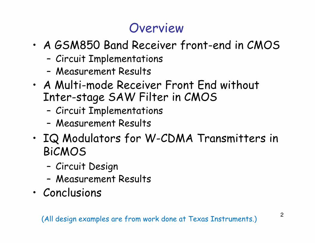
Overview• A GSM850 Band Receiver front-end in CMOS
– Circuit Implementations– Measurement Results
• A Multi-mode Receiver Front End without Inter-stage SAW Filter in CMOS– Circuit Implementations– Measurement Results
2
– Measurement Results
• IQ Modulators for W-CDMA Transmitters in BiCMOS– Circuit Design– Measurement Results
• Conclusions
(All design examples are from work done at Texas Instruments.)
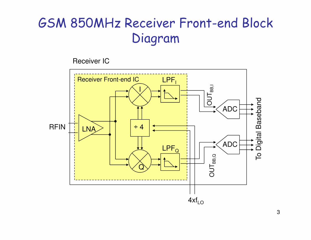
GSM 850MHz Receiver Front-end Block Diagram
LPFI
I
OU
TB
B,I
Receiver Front-end IC
ADC
Receiver IC
To D
igital B
aseband
3
LNA ÷ 4
LPFQ
Q
RFIN
4xfLO
OU
TB
B,Q
ADC
To D
igital B
aseband
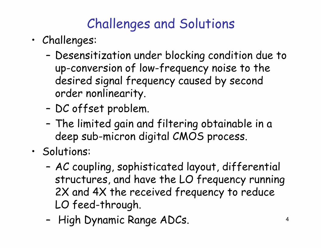
Challenges and Solutions• Challenges:
– Desensitization under blocking condition due to up-conversion of low-frequency noise to the desired signal frequency caused by second order nonlinearity.
– DC offset problem.
– The limited gain and filtering obtainable in a
4
– The limited gain and filtering obtainable in a deep sub-micron digital CMOS process.
• Solutions:
– AC coupling, sophisticated layout, differential structures, and have the LO frequency running 2X and 4X the received frequency to reduce LO feed-through.
– High Dynamic Range ADCs.
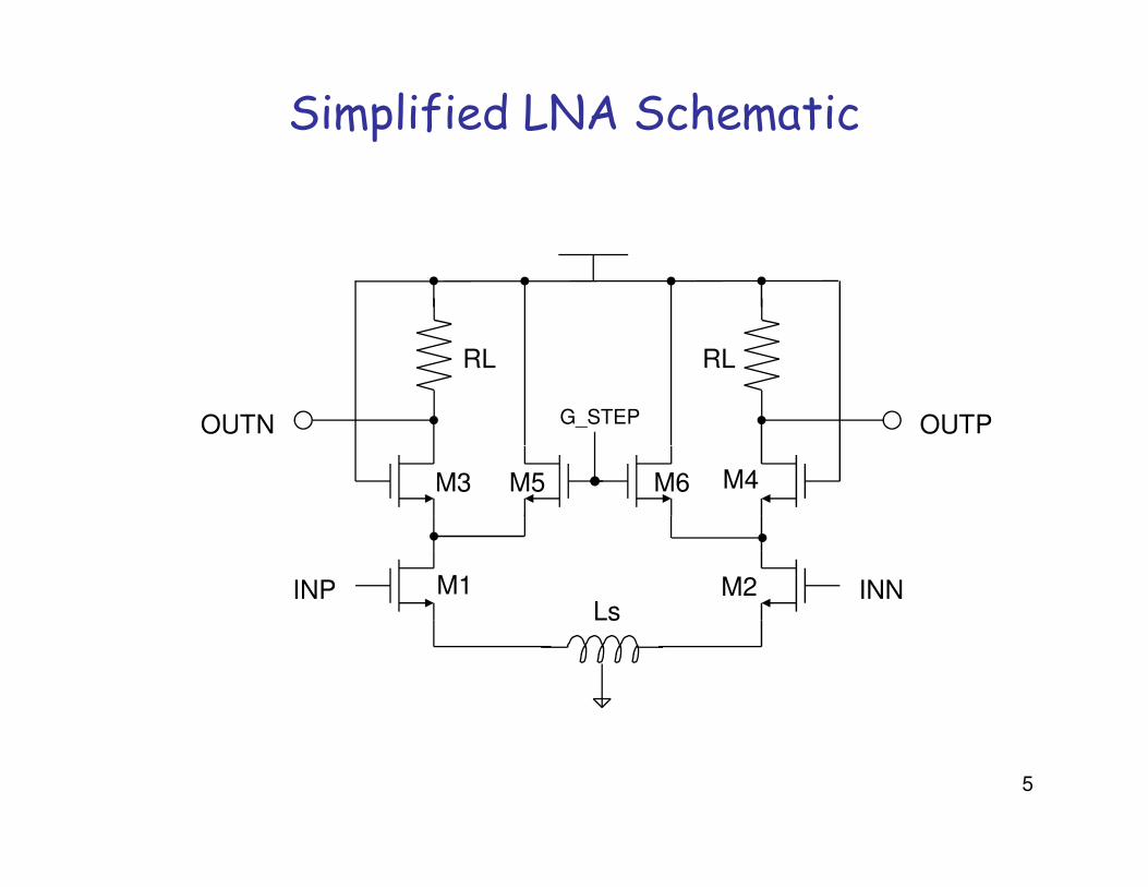
Simplified LNA Schematic
OUTN OUTP
RL RL
G_STEP
5
INP INNM1 M2
M3 M4
Ls
M6M5
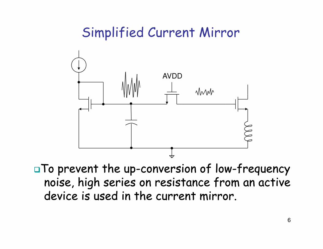
Simplified Current Mirror
AVDD
6
��To prevent the upTo prevent the up--conversion of lowconversion of low--frequency frequency noise, high series on resistance from an active noise, high series on resistance from an active device is used in the current mirror.device is used in the current mirror.
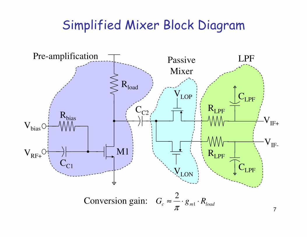
Simplified Mixer Block Diagram
Rbias
Rload
CC2
VLOP
V
RLPF
CLPF
Pre-amplification Passive
Mixer
LPF
7
Vbias
VRF+
Rbias
CC1
M1
VLON
VIF+
VIF-
RLPF
CLPF
loadmc RgG ⋅⋅≈ 1
2
πConversion gain:
Mixer Design
• AC coupling before and within the mixer prevents the contributions of mismatches in the LNA and the mixer pre-amplifiers to the DC offset.
• PMOS switches in the passive mixers
8
• PMOS switches in the passive mixers – i) facilitate easy DC coupling to the ADCs through
simple source followers, while ensuring complete switching with LO swing from 0v to 1.5V.
– ii) contribute less flicker noise to the mixer output noise;
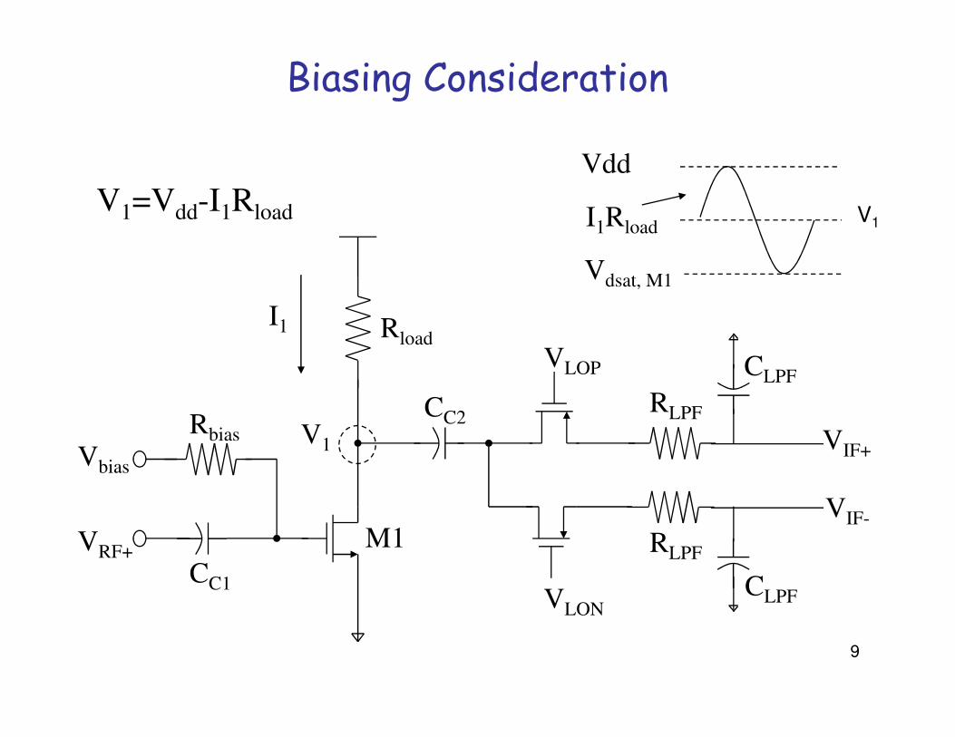
Biasing Consideration
Rload
VLOP CLPF
I1
V1=Vdd-I1Rload I1Rload
Vdd
Vdsat, M1
V1
9
Vbias
VRF+
Rbias
CC1
M1
CC2
VLOP
VLON
VIF+
VIF-
RLPF
RLPF
CLPF
CLPF
V1
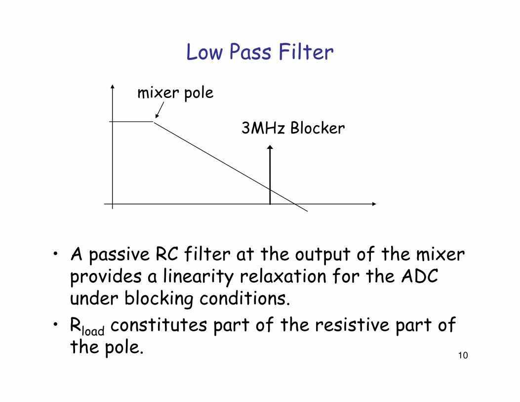
Low Pass Filter
3MHz Blocker
mixer pole
10
• A passive RC filter at the output of the mixer provides a linearity relaxation for the ADC under blocking conditions.
• Rload constitutes part of the resistive part of the pole.
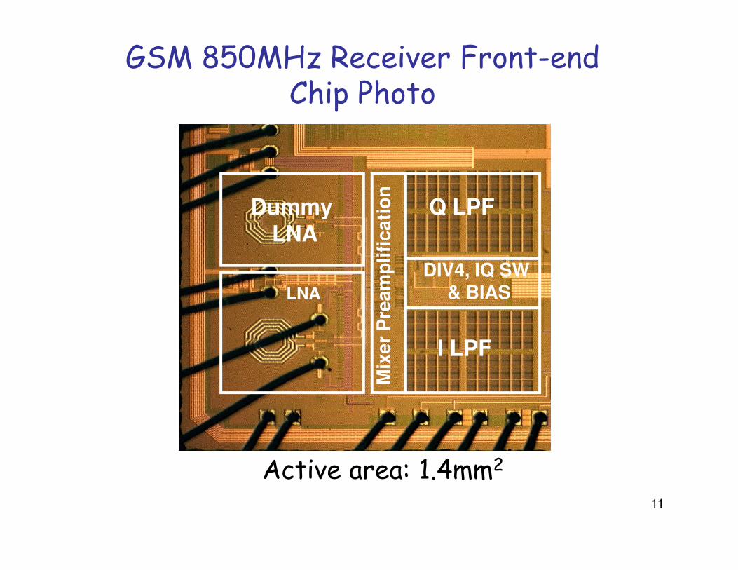
GSM 850MHz Receiver Front-end Chip Photo
Dummy LNA
LNA
Mix
er
Pre
am
plifi
ca
tio
n
Q LPF
DIV4, IQ SW & BIAS
11
LNA
Mix
er
Pre
am
plifi
ca
tio
n
I LPF
& BIAS
Active area: 1.4mm2
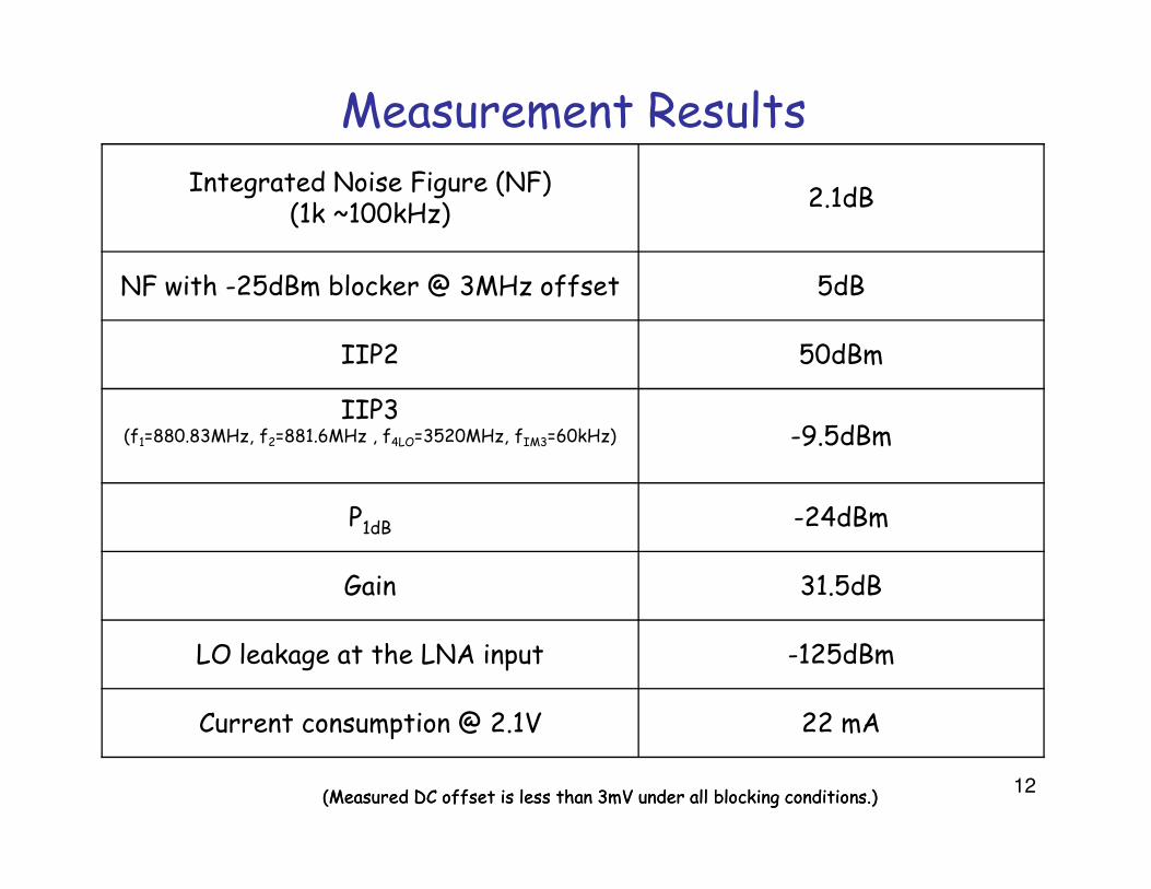
Measurement Results
Integrated Noise Figure (NF)(1k ~100kHz)
2.1dB
NF with -25dBm blocker @ 3MHz offset 5dB
IIP2 50dBm
IIP3(f1=880.83MHz, f2=881.6MHz , f4LO=3520MHz, fIM3=60kHz) -9.5dBm
12
(f1=880.83MHz, f2=881.6MHz , f4LO=3520MHz, fIM3=60kHz) -9.5dBm
P1dB -24dBm
Gain 31.5dB
LO leakage at the LNA input -125dBm
Current consumption @ 2.1V 22 mA
(Measured DC offset is less than 3mV under all blocking conditions.)(Measured DC offset is less than 3mV under all blocking conditions.)
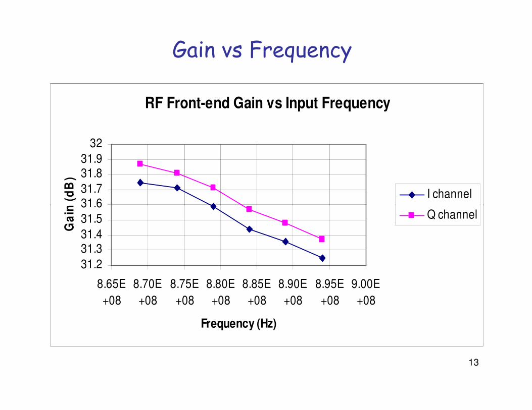
Gain vs Frequency
RF Front-end Gain vs Input Frequency
31.631.7
31.831.9
32
Ga
in (
dB
)
I channel
13
31.2
31.331.4
31.5
31.6
8.65E
+08
8.70E
+08
8.75E
+08
8.80E
+08
8.85E
+08
8.90E
+08
8.95E
+08
9.00E
+08
Frequency (Hz)
Ga
in (
dB
)
Q channel
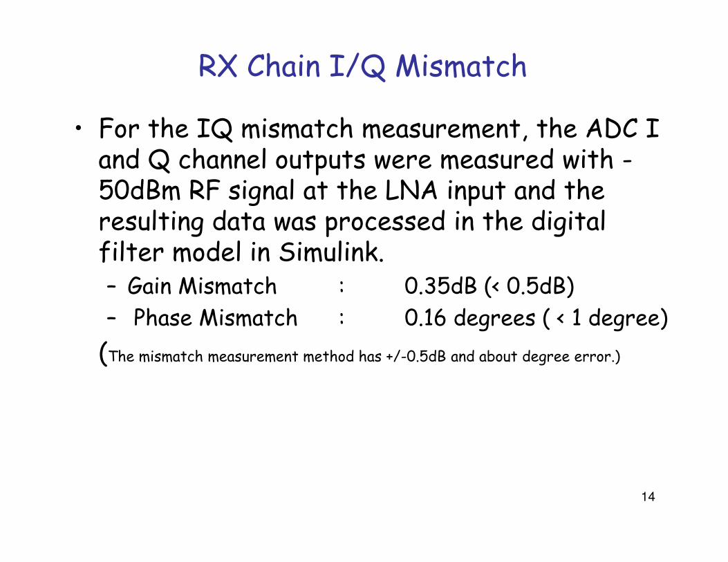
• For the IQ mismatch measurement, the ADC I and Q channel outputs were measured with -50dBm RF signal at the LNA input and the resulting data was processed in the digital filter model in Simulink.– Gain Mismatch : 0.35dB (< 0.5dB)
RX Chain I/Q Mismatch
14
– Gain Mismatch : 0.35dB (< 0.5dB)
– Phase Mismatch : 0.16 degrees ( < 1 degree)
(The mismatch measurement method has +/-0.5dB and about degree error.)
A Multi-Mode Receiver Front End
• A WCDMA, GSM/GPRS/EDGE Receiver Front End without Inter-stage SAW Filter was implemented :
15
implemented :– To reduce hardware in multi-band, multi-mode
transceivers.
– Establish that deep sub-micron CMOS is capable of RF performance and integration.
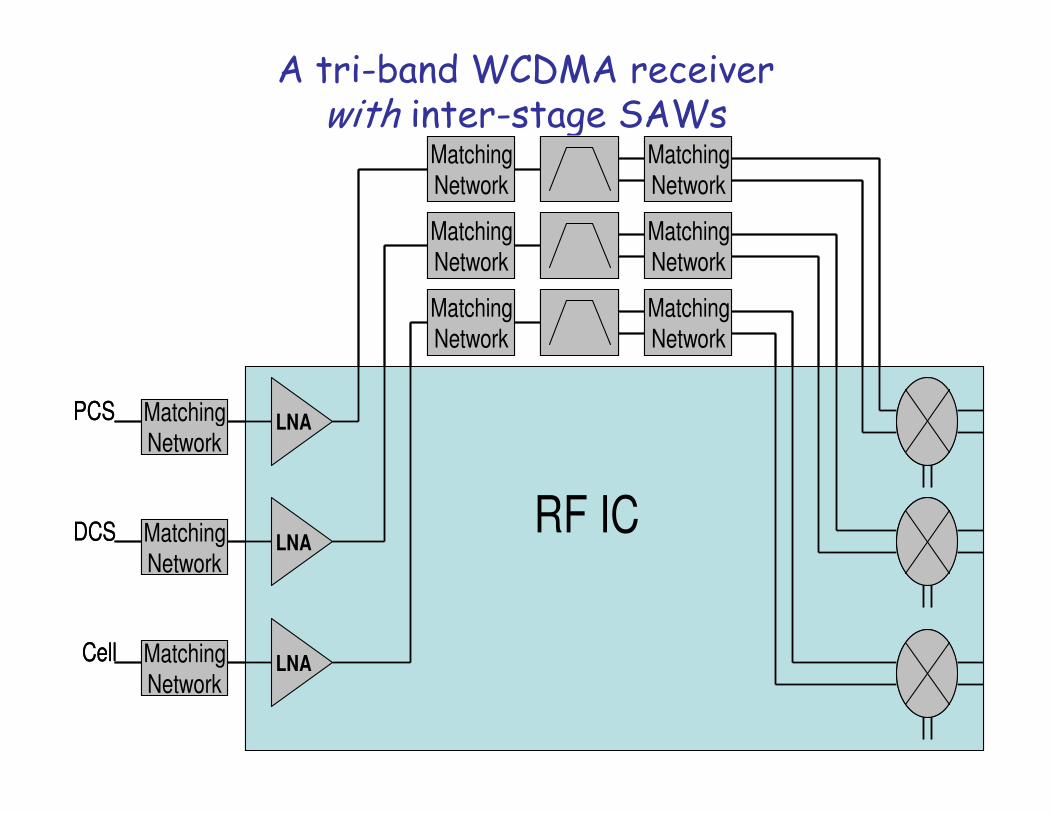
A tri-band WCDMA receiver with inter-stage SAWs
Matching
Matching
Network
Matching
Network
Matching
Network
Matching
Network
Matching
Network
Matching
Network
PCS Matching
Matching
Network
Matching
Network
Matching
Network
Matching
Network
Matching
Network
Matching
Network
PCS
16
LNAMatchingNetwork
LNAMatchingNetwork
LNAMatchingNetwork
PCS
DCS
Cell
RF IC
LNAMatchingNetwork
LNAMatchingNetwork
LNAMatchingNetwork
PCS
DCS
Cell
RF IC
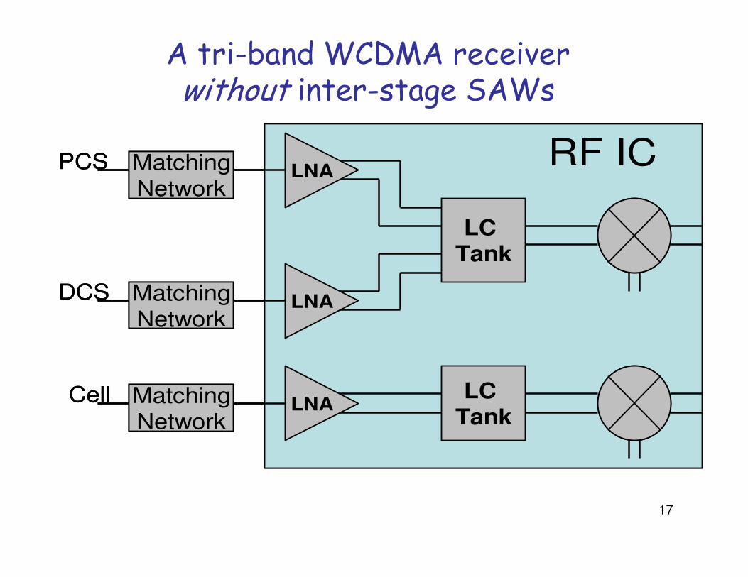
A tri-band WCDMA receiver without inter-stage SAWs
MatchingNetwork
Matching
LC Tank
LNAPCS
DCS
RF ICMatchingNetwork
Matching
LC Tank
LNAPCS
DCS
RF IC
17
MatchingNetwork
MatchingNetwork
LNA
LC Tank
LNA
DCS
Cell
MatchingNetwork
MatchingNetwork
LNA
LC Tank
LNA
DCS
Cell
Advantages of SAW removal in a tri band WCDMA receiver
• Integration– Saves 3 SAW filters
– 15 matching components
– 9 pins on the IC
– Board area
18
– Board area
• More suitable for RX path to be configured as dual mode (WCDMA/GGE)
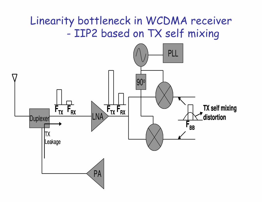
Linearity bottleneck in WCDMA receiver- IIP2 based on TX self mixing
PLL
90o
PLL
90o
19
LNADuplexer
PA
TX
Leakage
TX self mixing
distortionFTX FRX FRXFTX
FBB
LNADuplexer
PA
TX
Leakage
TX self mixing
distortionFTX FRX FRXFTX
FBB
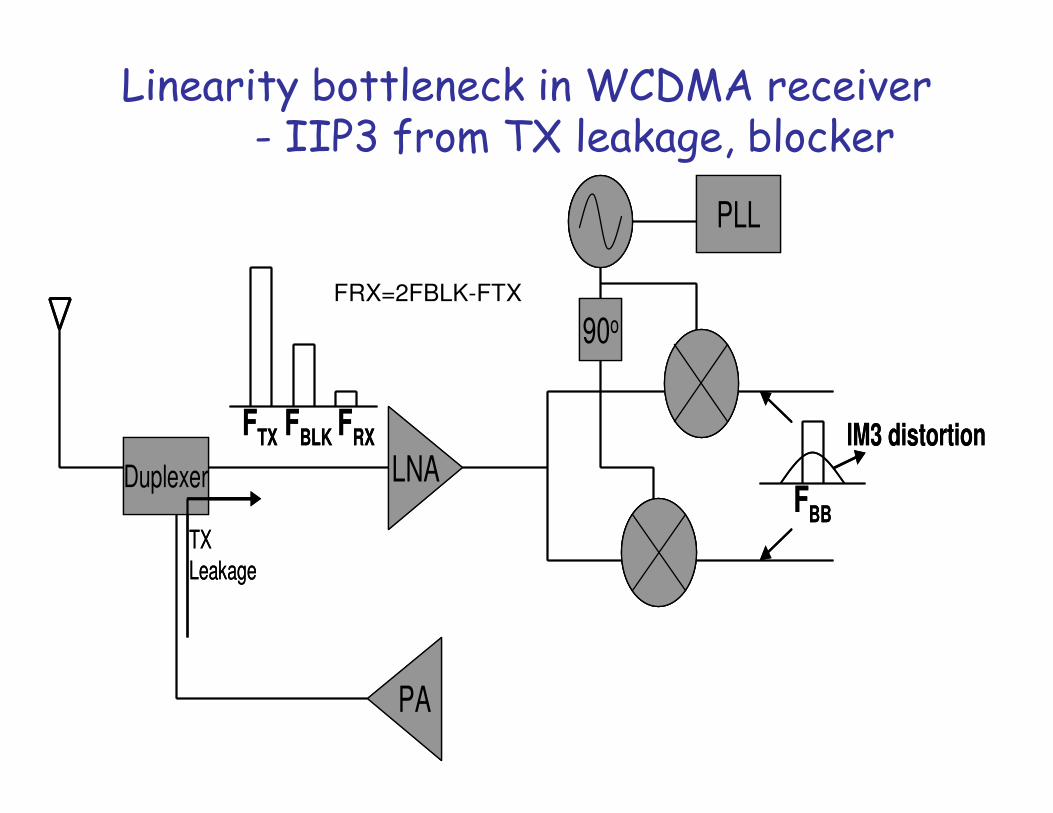
Linearity bottleneck in WCDMA receiver- IIP3 from TX leakage, blocker
PLL
90o
F F F
PLL
90o
F F F
FRX=2FBLK-FTX
20
LNADuplexer
PA
TX
Leakage
IM3 distortionFTX
FBB
FBLK FRX
LNADuplexer
PA
TX
Leakage
IM3 distortionFTX
FBB
FBLK FRX
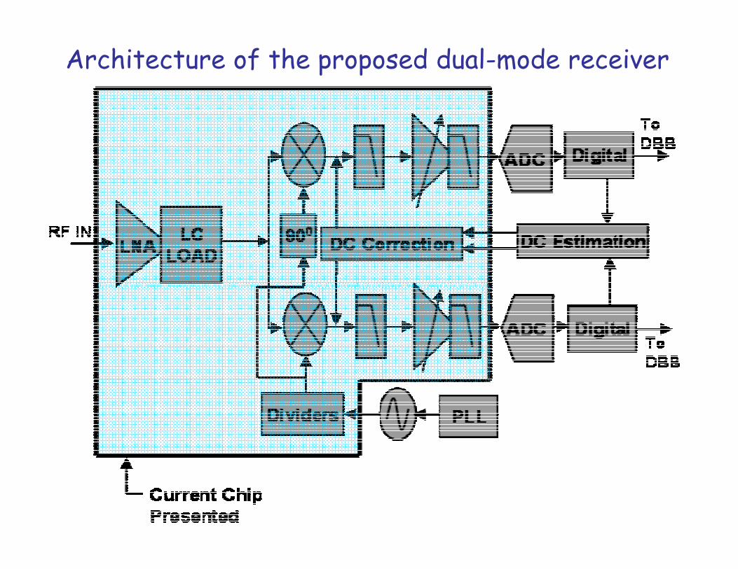
Architecture of the proposed dual-mode receiver
21
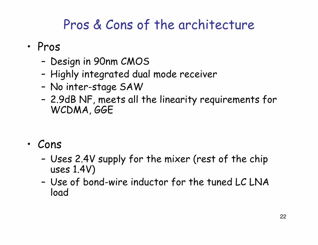
Pros & Cons of the architecture
• Pros– Design in 90nm CMOS– Highly integrated dual mode receiver– No inter-stage SAW– 2.9dB NF, meets all the linearity requirements for
WCDMA, GGE
22
• Cons – Uses 2.4V supply for the mixer (rest of the chip
uses 1.4V)– Use of bond-wire inductor for the tuned LC LNA
load
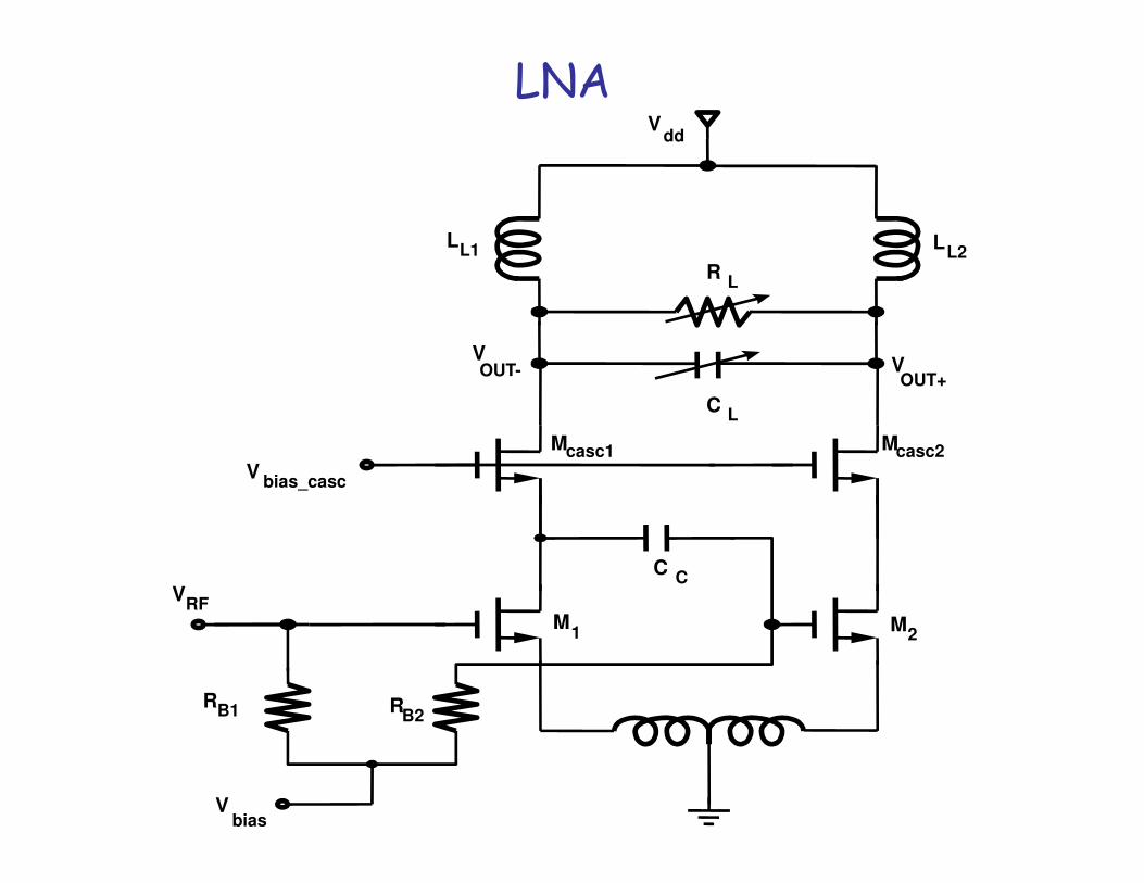
LNA
RL
VOUT+
Mcasc1
Vdd
CL
VOUT-
Mcasc2
LL1 L
L2
23
Mcasc1
VRF
RB1
M1
Vbias
Vbias_casc
M2
Mcasc2
RB2
CC
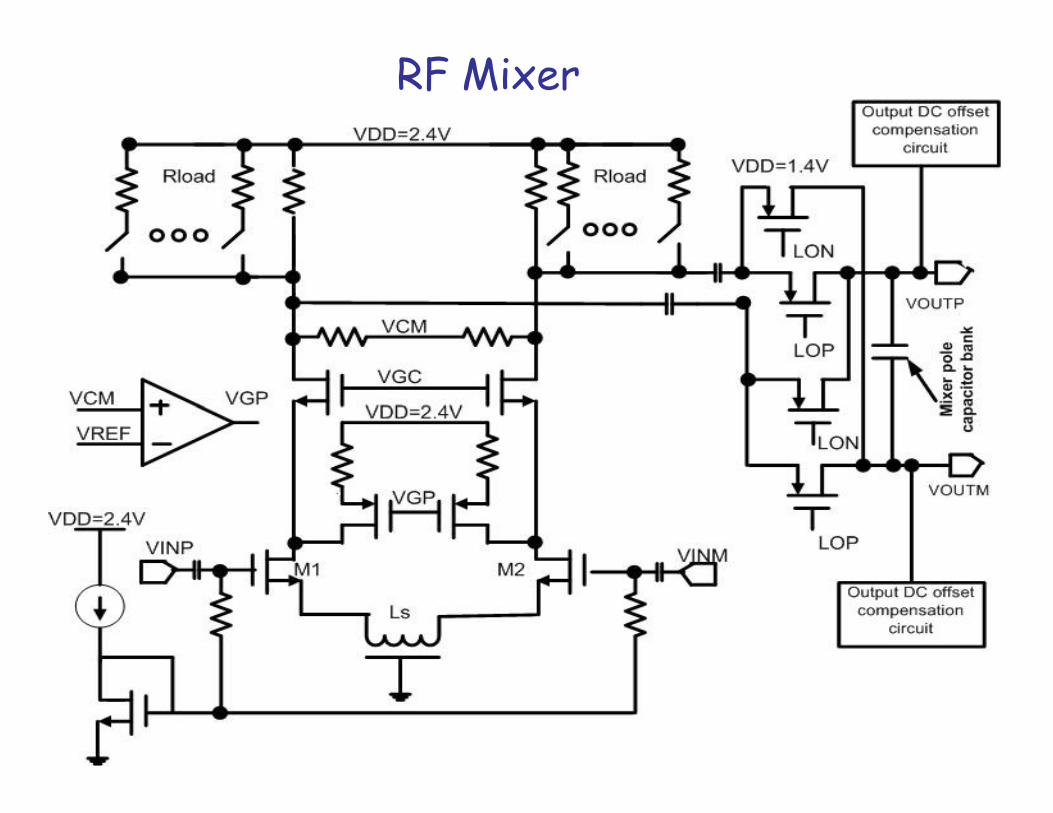
RF Mixer
24
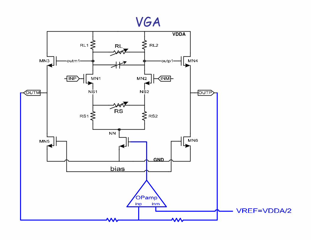
VDDA
VGA
25
GND
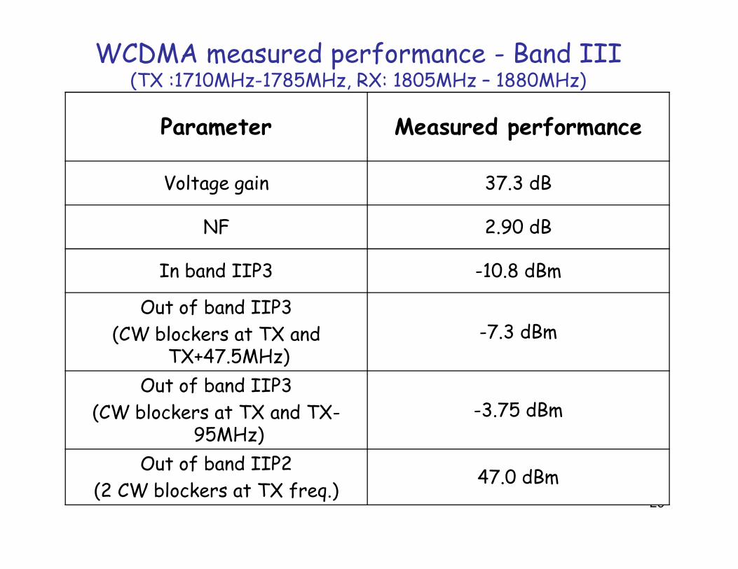
WCDMA measured performance - Band III(TX :1710MHz-1785MHz, RX: 1805MHz – 1880MHz)
Parameter Measured performance
Voltage gain 37.3 dB
NF 2.90 dB
In band IIP3 -10.8 dBm
26
Out of band IIP3
(CW blockers at TX and TX+47.5MHz)
-7.3 dBm
Out of band IIP3
(CW blockers at TX and TX-95MHz)
-3.75 dBm
Out of band IIP2
(2 CW blockers at TX freq.)47.0 dBm
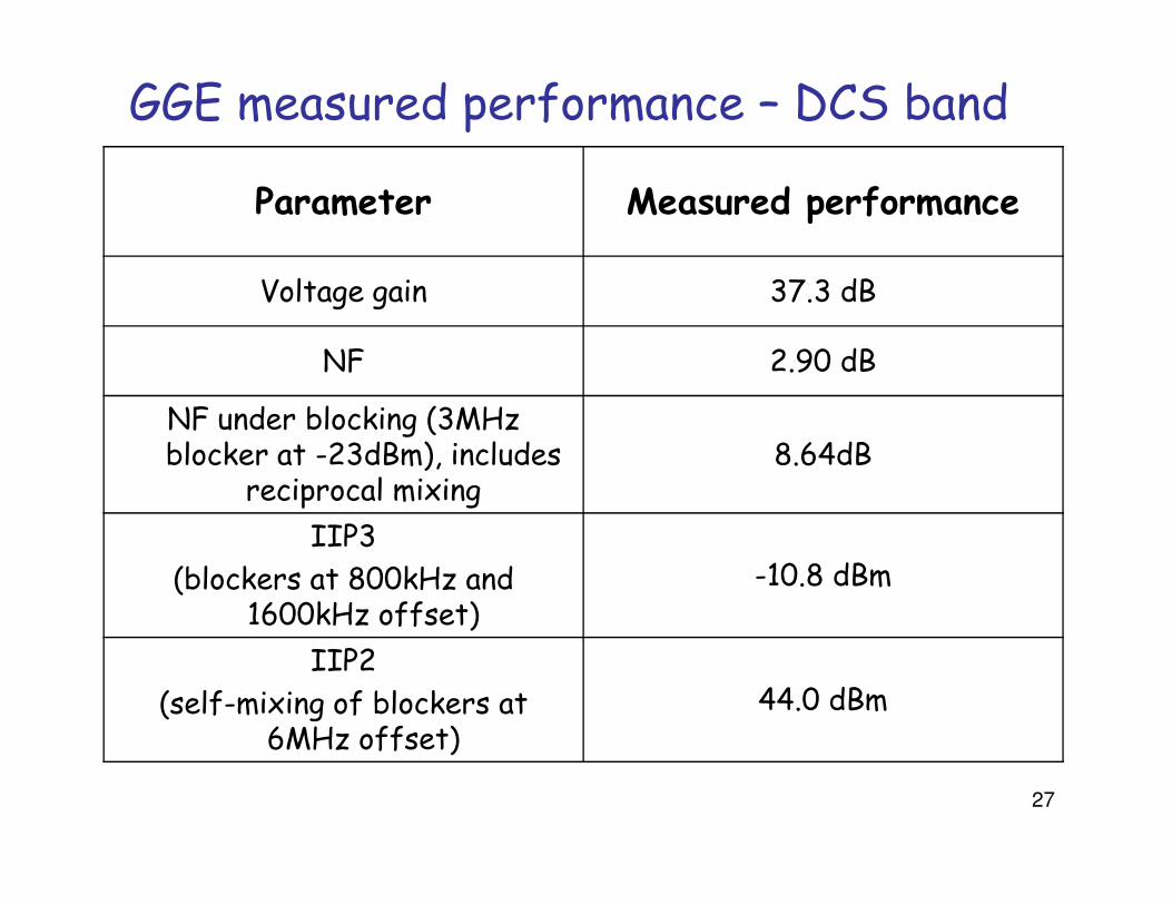
GGE measured performance – DCS band
Parameter Measured performance
Voltage gain 37.3 dB
NF 2.90 dB
NF under blocking (3MHz blocker at -23dBm), includes 8.64dB
27
blocker at -23dBm), includes reciprocal mixing
8.64dB
IIP3
(blockers at 800kHz and 1600kHz offset)
-10.8 dBm
IIP2
(self-mixing of blockers at 6MHz offset)
44.0 dBm
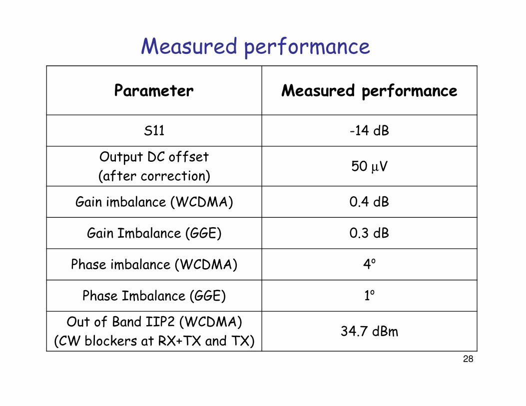
Measured performance
Parameter Measured performance
S11 -14 dB
Output DC offset
(after correction)50 µV
Gain imbalance (WCDMA) 0.4 dB
28
Gain imbalance (WCDMA) 0.4 dB
Gain Imbalance (GGE) 0.3 dB
Phase imbalance (WCDMA) 4o
Phase Imbalance (GGE) 1o
Out of Band IIP2 (WCDMA)
(CW blockers at RX+TX and TX)34.7 dBm
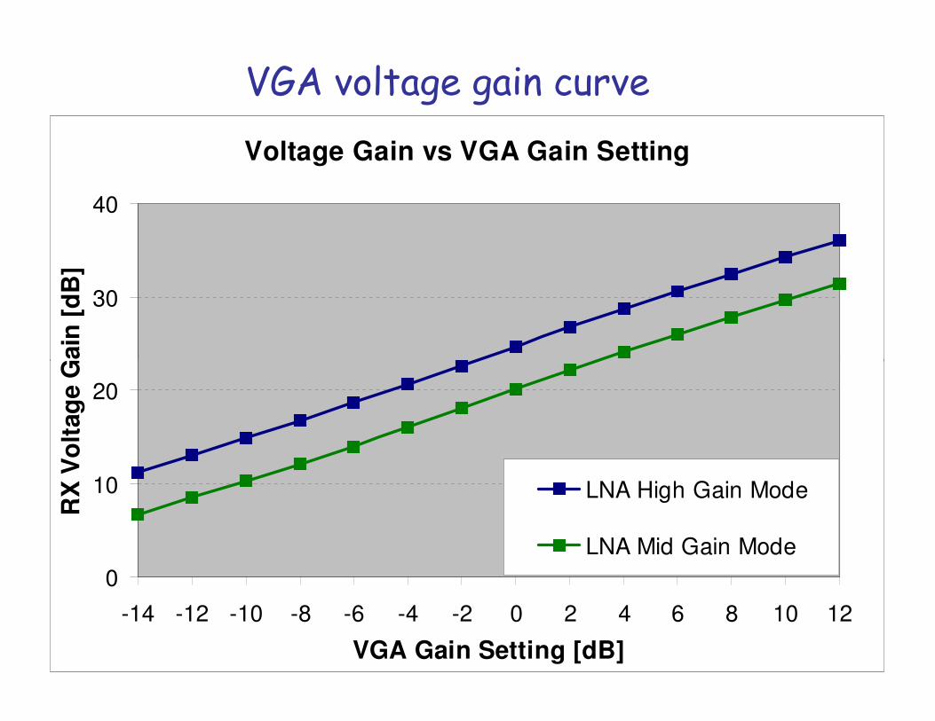
VGA voltage gain curve
Voltage Gain vs VGA Gain Setting
30
40
RX
Vo
ltag
e G
ain
[d
B]
29
0
10
20
-14 -12 -10 -8 -6 -4 -2 0 2 4 6 8 10 12
VGA Gain Setting [dB]
RX
Vo
ltag
e G
ain
[d
B]
LNA High Gain Mode
LNA Mid Gain Mode
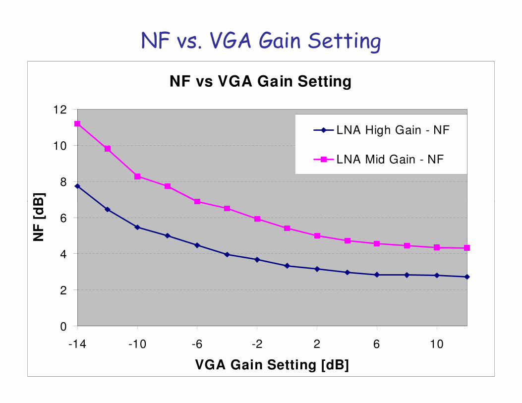
NF vs. VGA Gain Setting
NF vs VGA Gain Setting
8
10
12
NF
[d
B]
LNA High Gain - NF
LNA Mid Gain - NF
30
0
2
4
6
-14 -10 -6 -2 2 6 10
VGA Gain Setting [dB]
NF
[d
B]
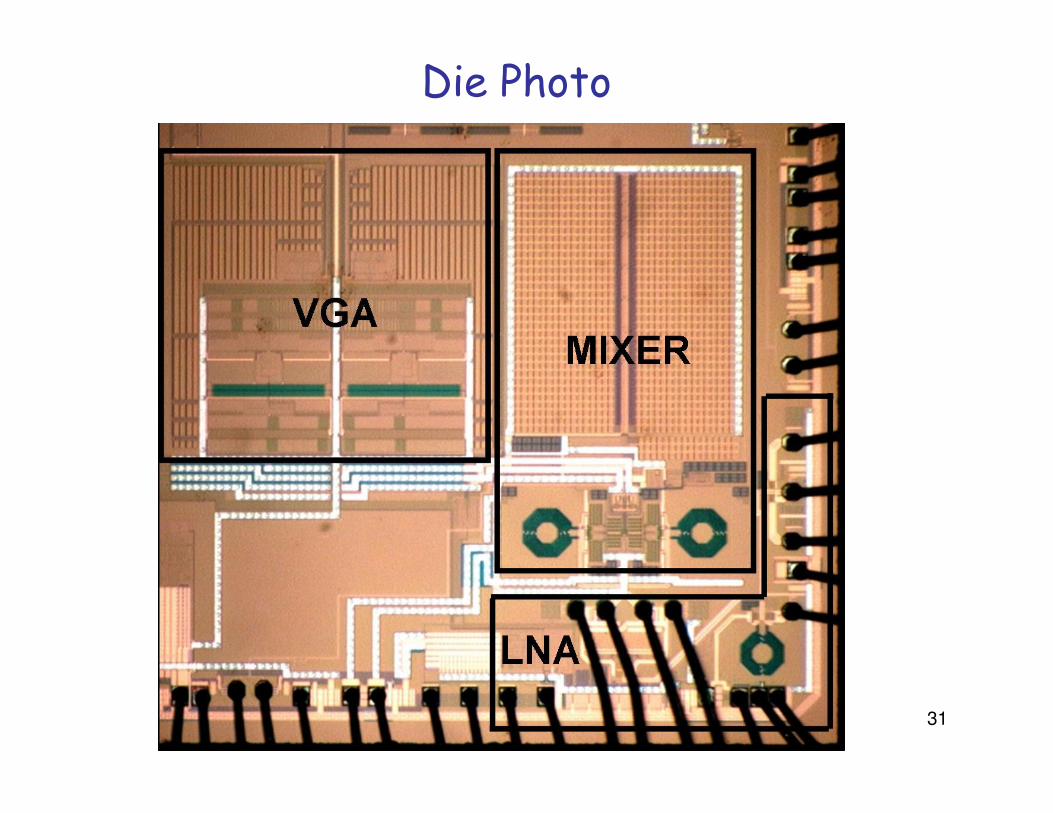
Die Photo
31
W-CDMA Transmitters
• The W-CDMA (Wideband Code Division Multiple Access) systems are popular due to their ability to deliver high data rates of up to 384kb/s at wide-area applications or even 2Mb/s indoors.
• The high degree of amplitude variation in the W-CDMA signals require very high linearity in
32
• The high degree of amplitude variation in the W-CDMA signals require very high linearity in the transceivers.
• An important challenge is the TX noise at the receive band due to full FDD (frequency-division duplex) nature of the transceiver, meaning both the TX and the RX are on at the same time.
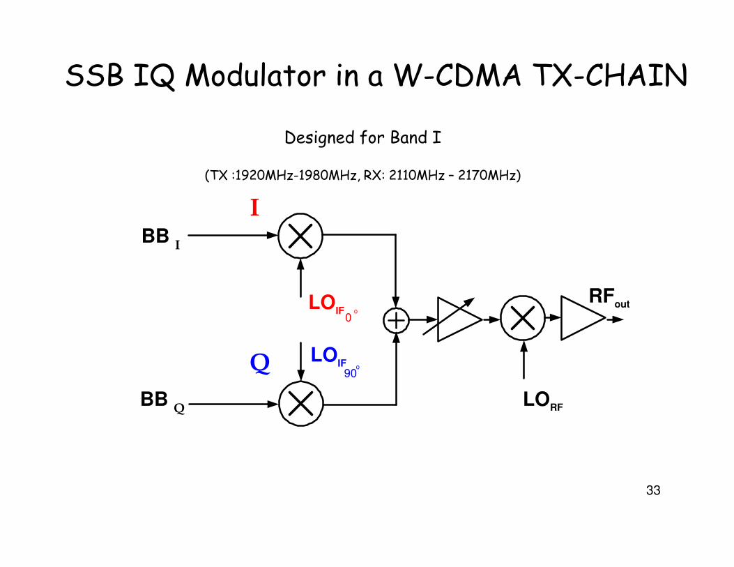
SSB IQ Modulator in a W-CDMA TX-CHAIN
BB I
I
Designed for Band I
(TX :1920MHz-1980MHz, RX: 2110MHz – 2170MHz)
33
BB Q
Q
LOIF
0o
LOIF
90o
LORF
RFout
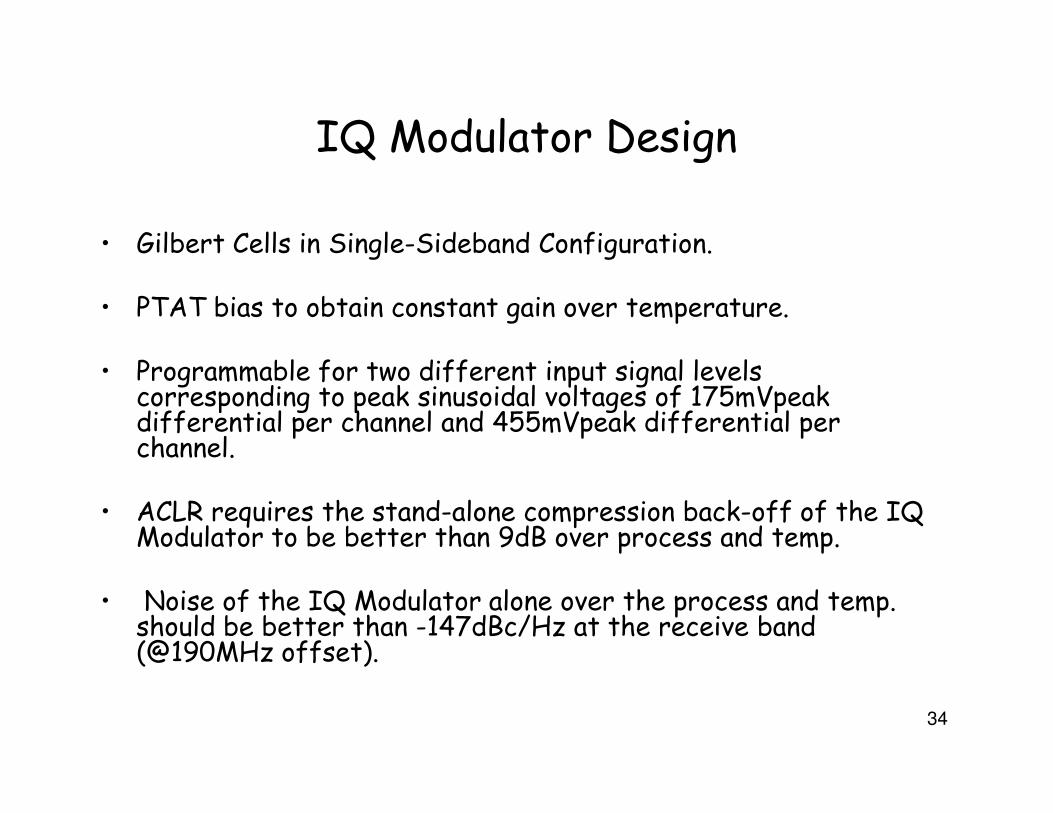
IQ Modulator Design
• Gilbert Cells in Single-Sideband Configuration.
• PTAT bias to obtain constant gain over temperature.
• Programmable for two different input signal levels corresponding to peak sinusoidal voltages of 175mVpeak differential per channel and 455mVpeak differential per
34
corresponding to peak sinusoidal voltages of 175mVpeak differential per channel and 455mVpeak differential per channel.
• ACLR requires the stand-alone compression back-off of the IQ Modulator to be better than 9dB over process and temp.
• Noise of the IQ Modulator alone over the process and temp. should be better than -147dBc/Hz at the receive band (@190MHz offset).
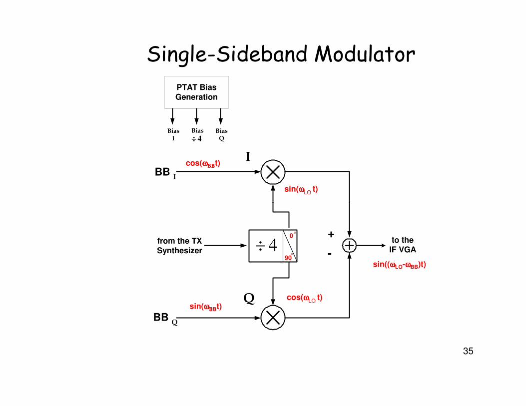
Single-Sideband Modulator
sin(ωωωωLO t)
BB I
I
PTAT Bias
Generation
Bias
I
Bias
Q
Bias
4÷÷÷÷
cos(ωωωωΒΒΒΒΒΒΒΒt)
35
4÷0
o
to theIF VGA
cos(ωωωωLO t)
BB Q
Q
from the TXSynthesizer
90o
+
-
sin(ωωωωΒΒΒΒΒΒΒΒt)
sin((ωωωωLO-ωωωωBB)t)
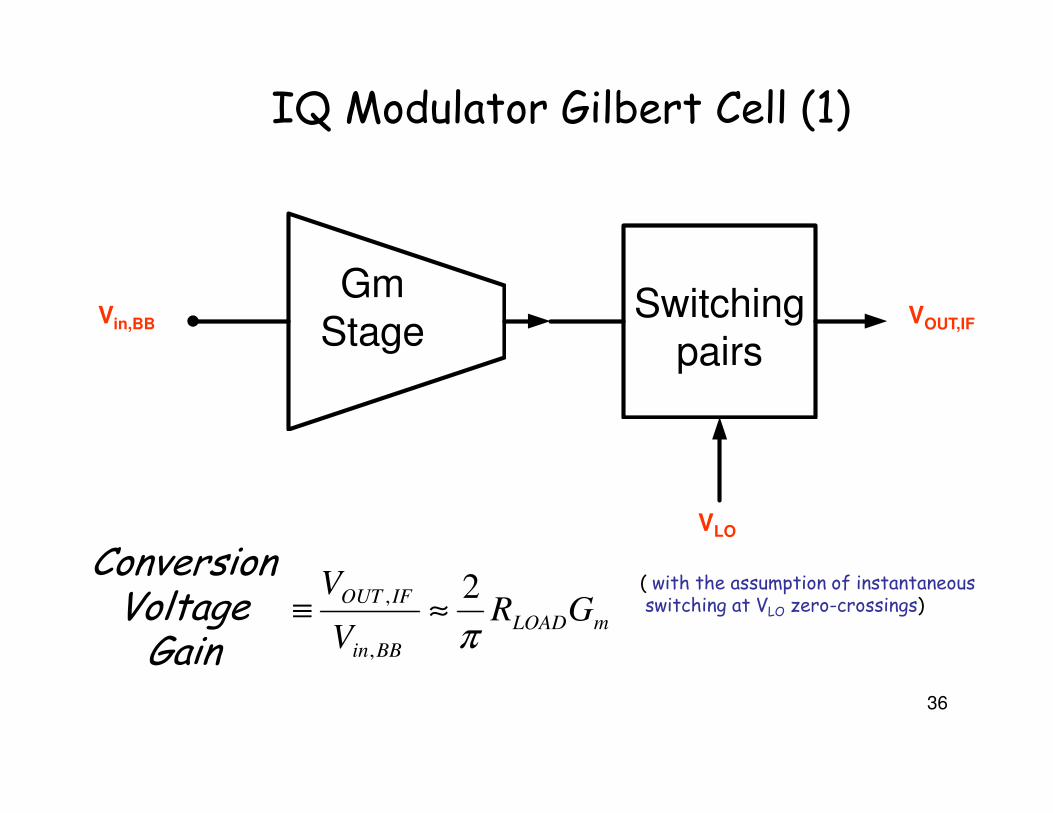
IQ Modulator Gilbert Cell (1)
Gm
StageSwitching
pairsVin,BB VOUT,IF
36
VLO
mLOAD
BBin
IFOUTGR
V
V
π
2
,
,≈≡
ConversionVoltage
Gain
( with the assumption of instantaneous switching at VLO zero-crossings)
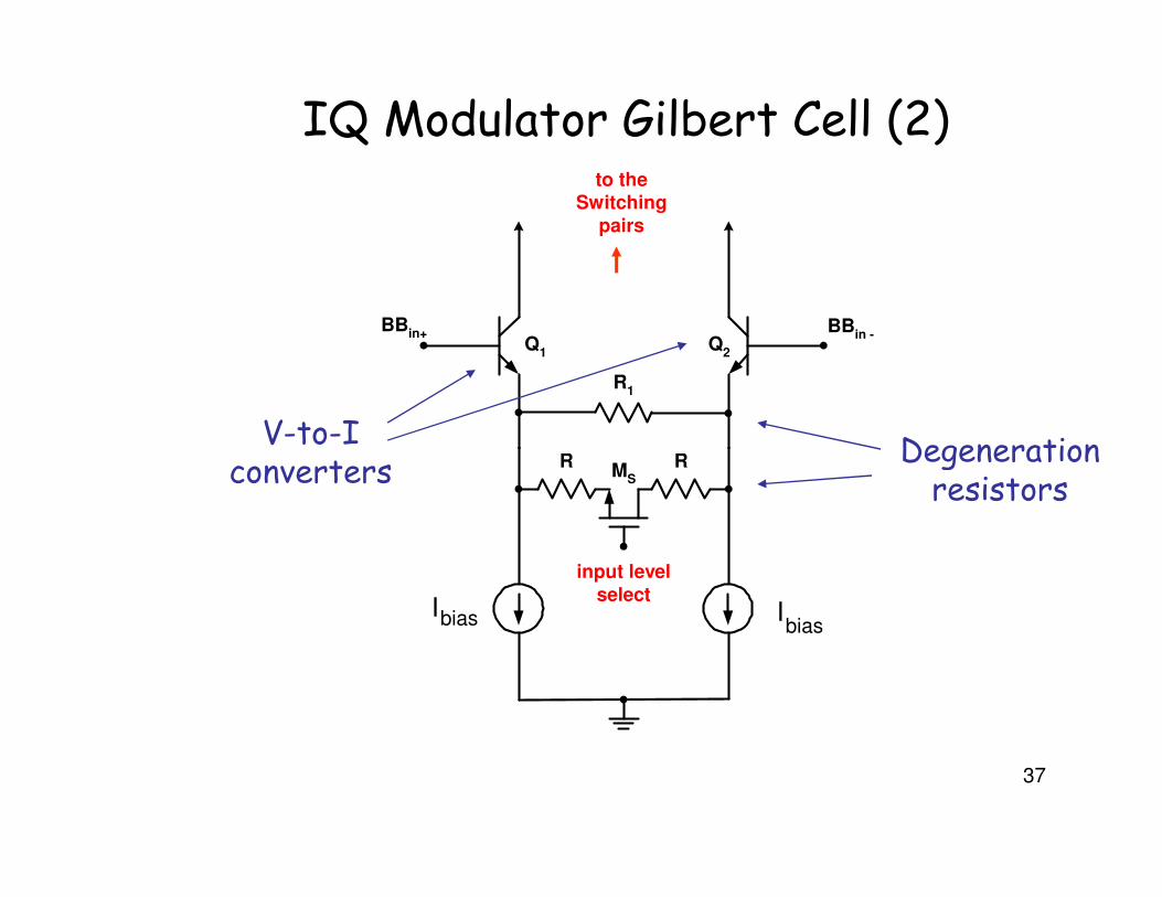
IQ Modulator Gilbert Cell (2)to the
Switching
pairs
BBin+ BB
in -Q
1Q
2
R1
DegenerationV-to-I
converters
37
input level
select
R RM
S
Degenerationresistors
V-to-Iconverters
Ibias Ibias
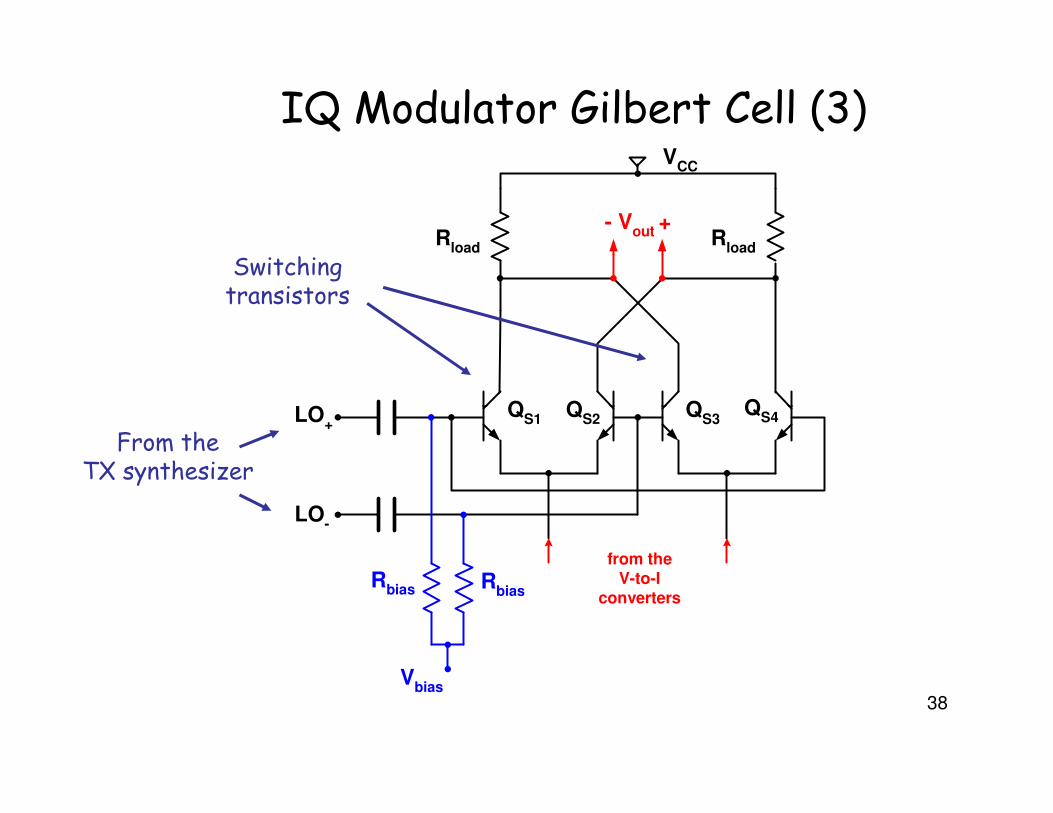
IQ Modulator Gilbert Cell (3)
QQ QQ
Rload
Rload
LO
VCC
- Vout
+
Switchingtransistors
38
QS2
QS1
QS4Q
S3LO+
LO-
Rbias R
bias
Vbias
from theV-to-I
converters
From theTX synthesizer
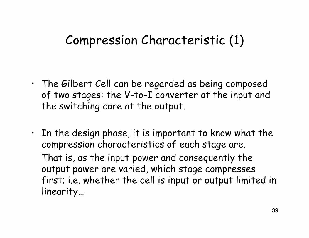
Compression Characteristic (1)
• The Gilbert Cell can be regarded as being composed of two stages: the V-to-I converter at the input and the switching core at the output.
39
• In the design phase, it is important to know what the compression characteristics of each stage are.
That is, as the input power and consequently the output power are varied, which stage compresses first; i.e. whether the cell is input or output limited in linearity…
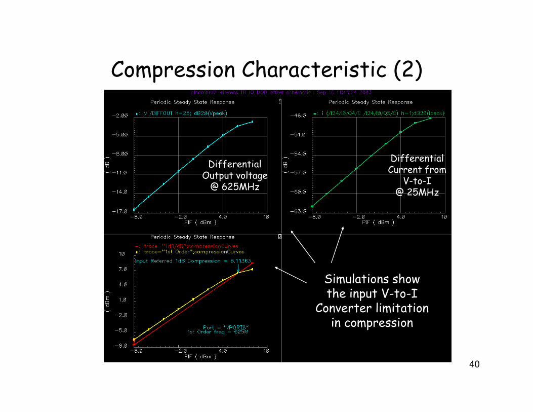
Compression Characteristic (2)
DifferentialOutput voltage
@ 625MHz
DifferentialCurrent from
V-to-I@ 25MHz
40
Simulations showthe input V-to-I
Converter limitationin compression
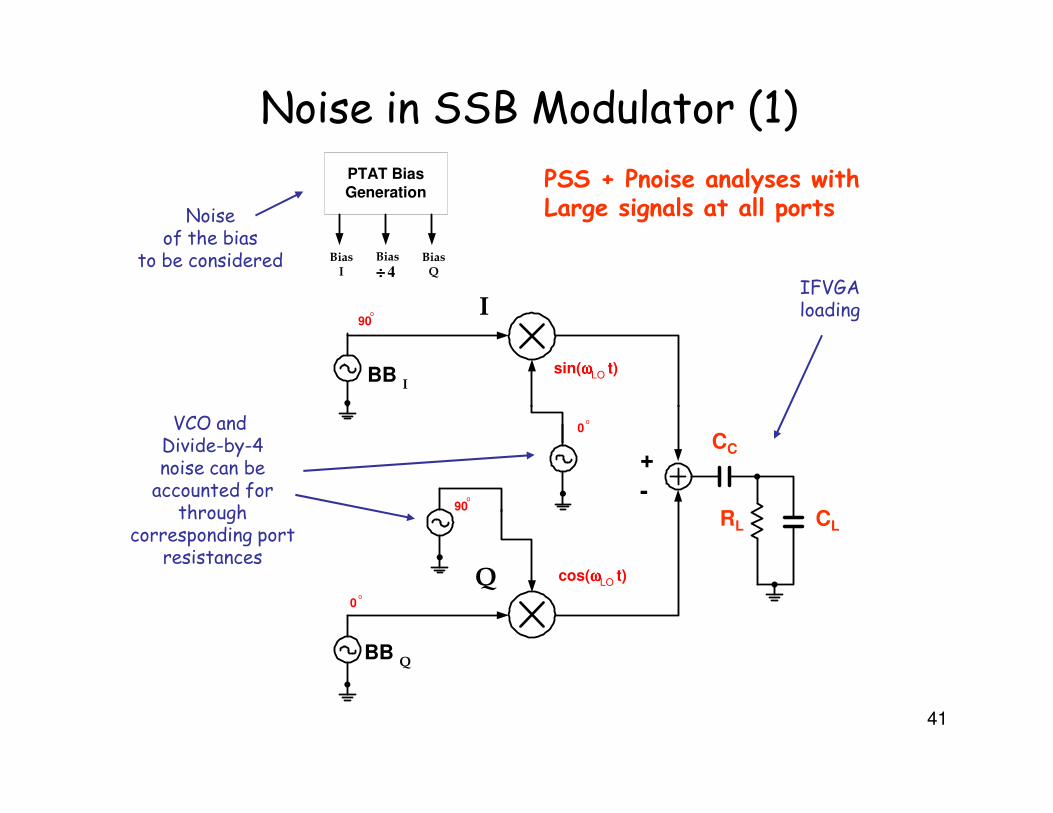
Noise in SSB Modulator (1)
sin(ωωωωLO t)BB
I
I
PTAT Bias
Generation
Bias
I
Bias
Q
Bias
4÷÷÷÷
90o
IFVGAloading
Noiseof the bias
to be considered
PSS + Pnoise analyses withLarge signals at all ports
41
cos(ωωωωLO t)
BB Q
Q0
o
90o
0o
CLRL
VCO and Divide-by-4noise can be
accounted forthrough
corresponding portresistances
+
-
CC
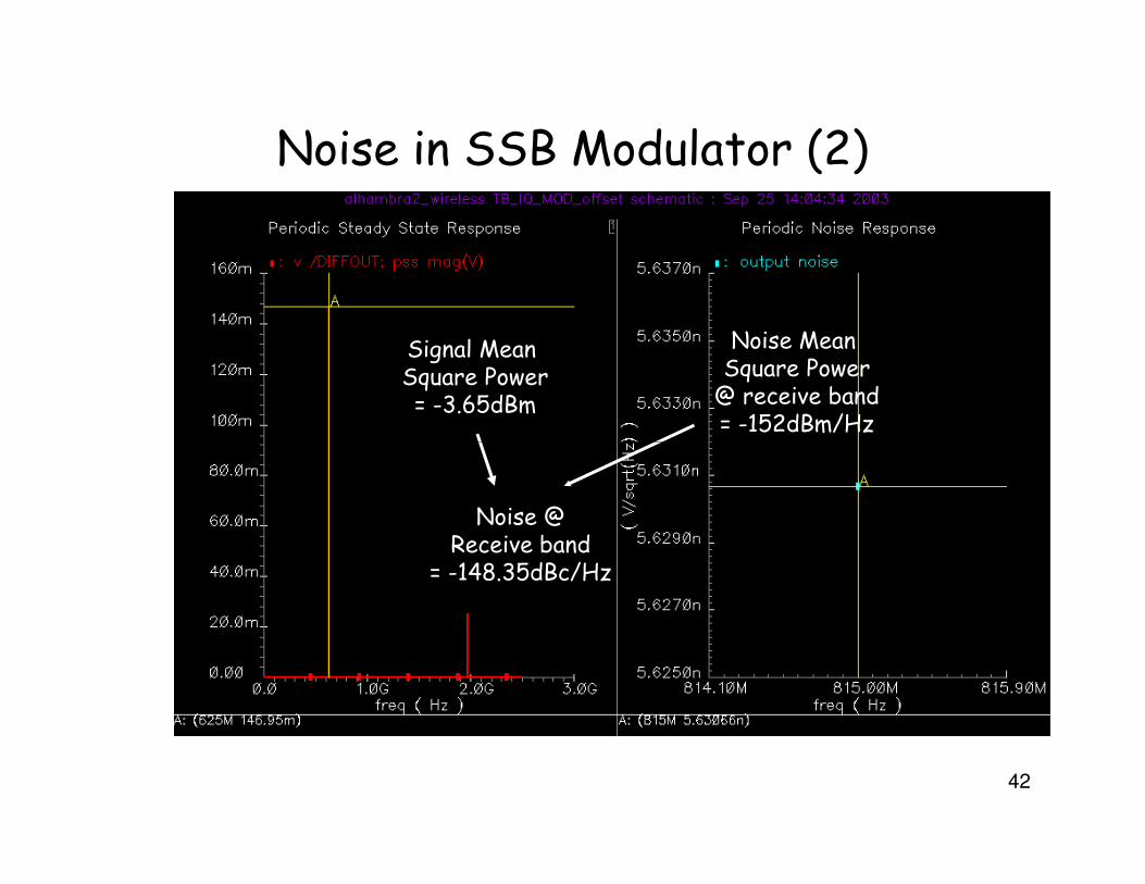
Noise in SSB Modulator (2)
Signal Mean Square Power= -3.65dBm
Noise Mean Square Power
@ receive band= -152dBm/Hz
42
Noise @Receive band
= -148.35dBc/Hz
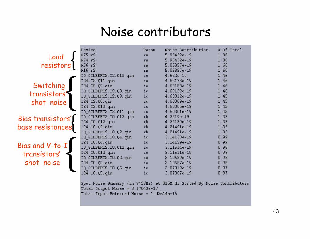
Noise contributors
{
{{
Loadresistors
Switchingtransistors’ shot noise
Bias transistors’
43
{{Bias transistors’
base resistances
Bias and V-to-Itransistors’ shot noise
Linearity and Noise vs. LO Drive (1)
• The amplitude of the quadrature LO (Local Oscillator) signal driving the SSB Modulator affects the linearity and the noise performances.
44
• As the level of LO drive becomes higher, the noise contribution of the switches in the cell becomes less due to the switch transistors staying on for less amount of time decreasing the overall noise.
• On the other hand, as the drive level increases, the compression at the mixer cell becomes more severe.
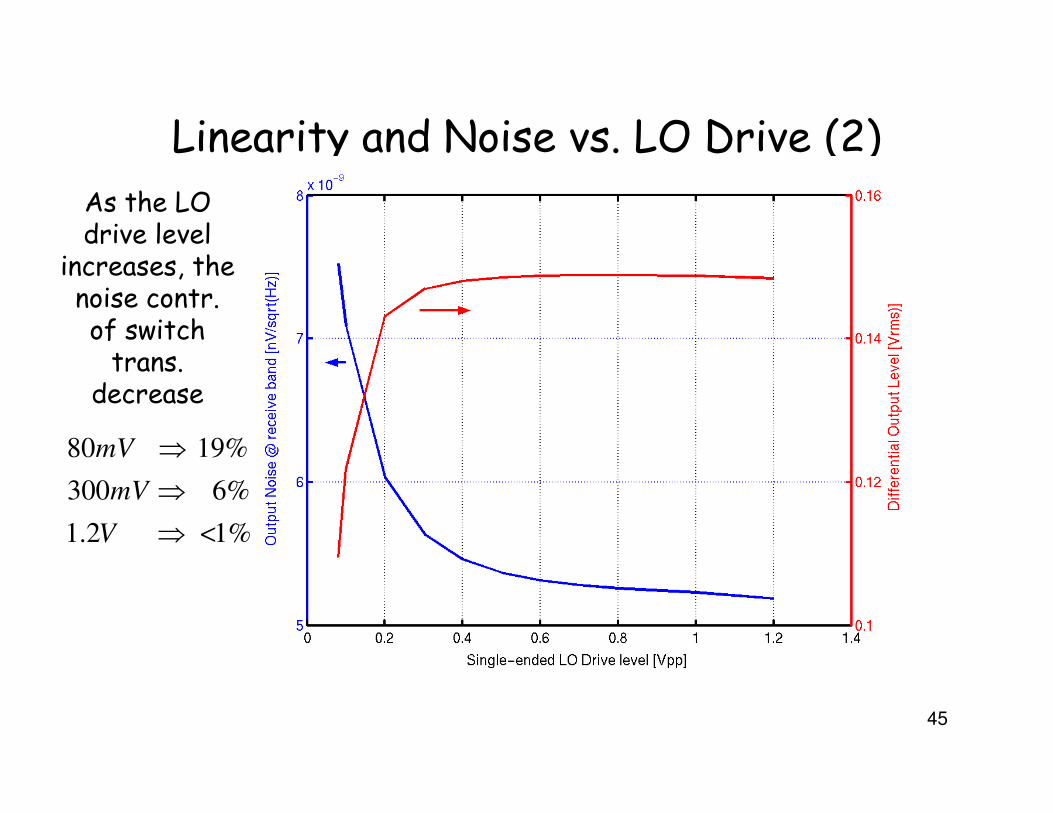
Linearity and Noise vs. LO Drive (2)
As the LO drive level
increases, the noise contr. of switch
trans. decrease
45
decrease
%12.1
%6300
%1980
<⇒
⇒
⇒
V
mV
mV
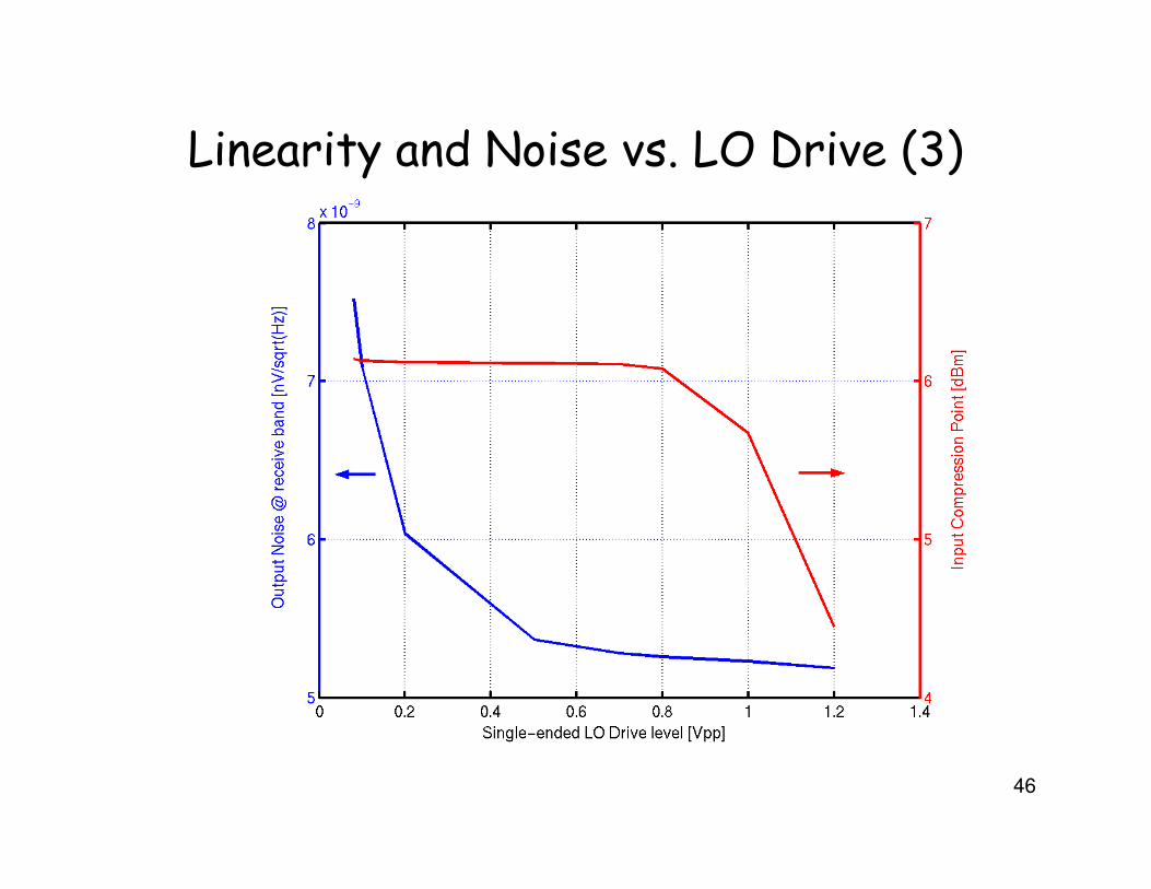
Linearity and Noise vs. LO Drive (3)
46
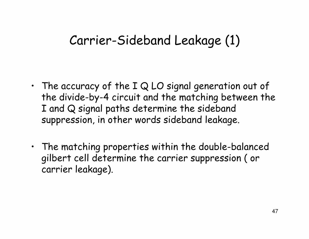
Carrier-Sideband Leakage (1)
• The accuracy of the I Q LO signal generation out of the divide-by-4 circuit and the matching between the I and Q signal paths determine the sideband suppression, in other words sideband leakage.
47
suppression, in other words sideband leakage.
• The matching properties within the double-balanced gilbert cell determine the carrier suppression ( or carrier leakage).
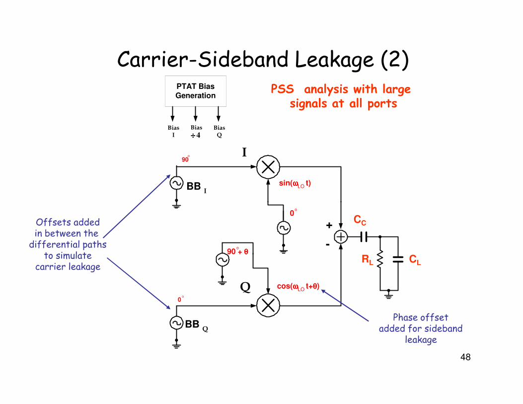
Carrier-Sideband Leakage (2)
sin(ωωωωLO t)BB
I
I
PTAT Bias
Generation
Bias
I
Bias
Q
Bias
4÷÷÷÷
90o
PSS analysis with large signals at all ports
48
cos(ωωωωLO t+θθθθ)
BB Q
Q0
o
90 +o
0o
θθθθ
+
-
Phase offsetadded for sideband
leakage
Offsets addedin between the
differential pathsto simulate
carrier leakage
CC
CLRL
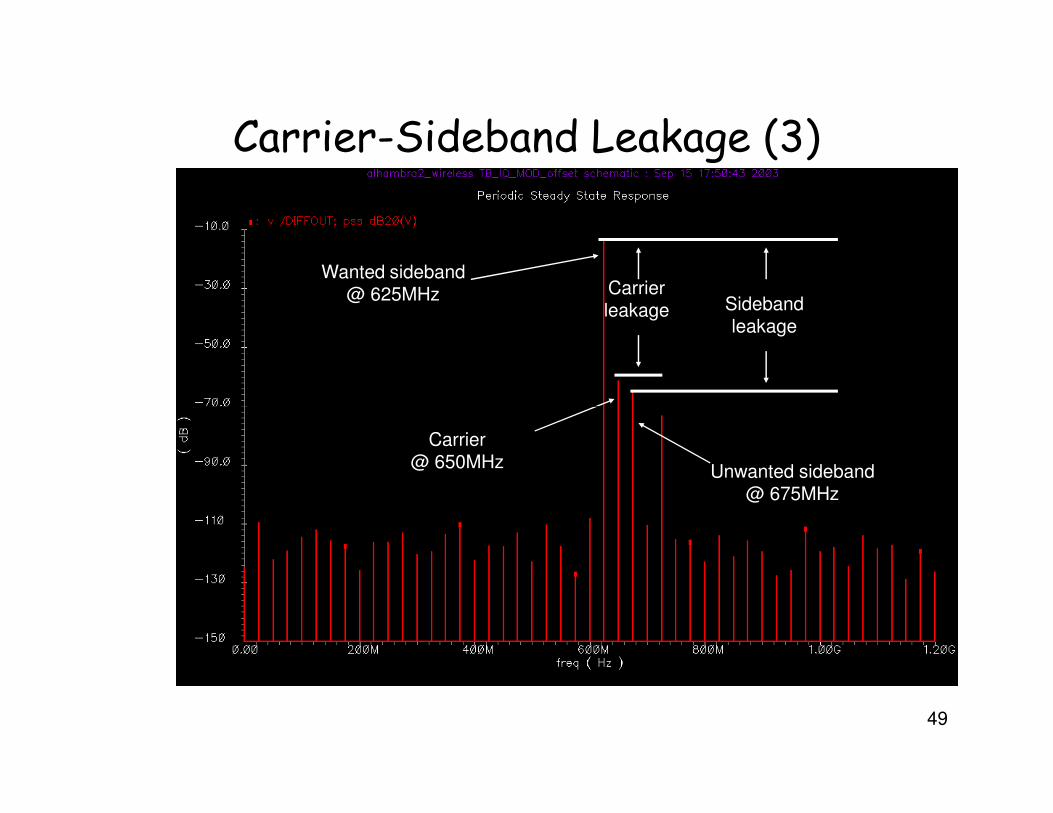
Carrier-Sideband Leakage (3)
Carrierleakage Sideband
leakage
Wanted sideband@ 625MHz
49
Carrier@ 650MHz
Unwanted sideband@ 675MHz
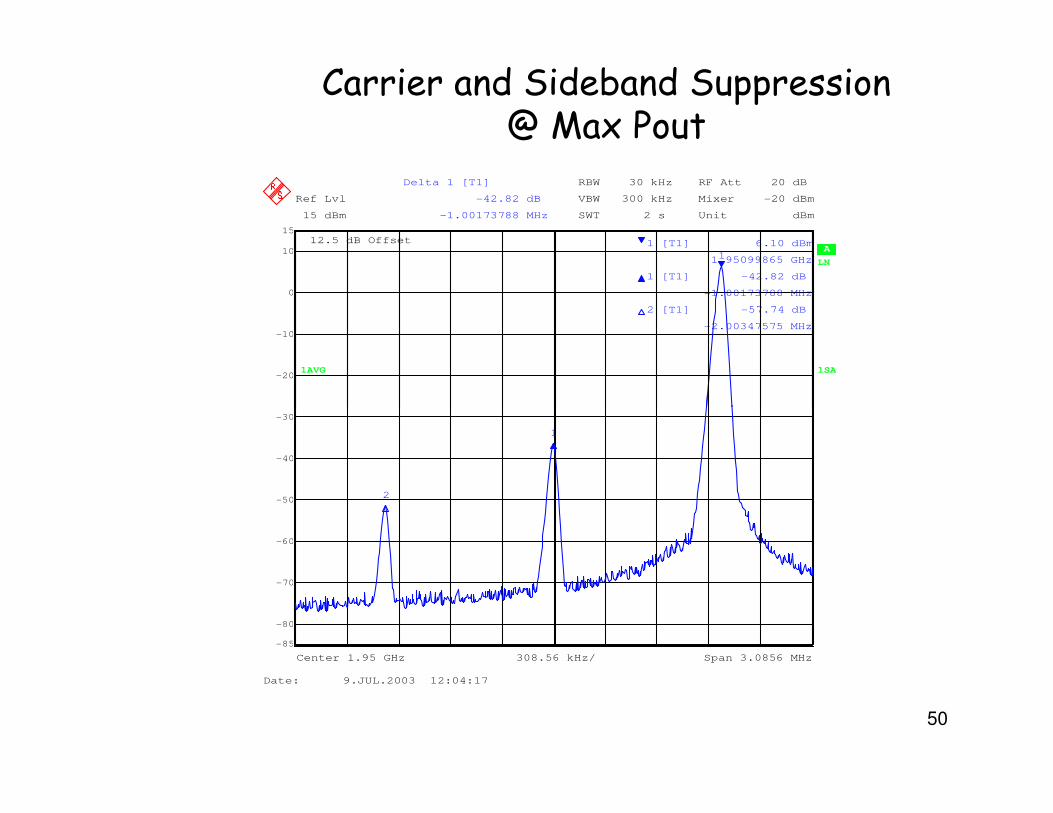
Carrier and Sideband Suppression@ Max Pout
SWT 2 s
A
LN
Unit dBm
Mixer -20 dBm
LN
12.5 dB Offset
Ref Lvl
15 dBm
Ref Lvl
15 dBm
RF Att 20 dBRBW 30 kHz
1AVG
VBW 300 kHz
1SA -20
-10
0
10
15
1
Delta 1 [T1]
-42.82 dB
-1.00173788 MHz
1 [T1] 6.10 dBm
1.95099865 GHz
1 [T1] -42.82 dB
-1.00173788 MHz
2 [T1] -57.74 dB
-2.00347575 MHz
50
Center 1.95 GHz Span 3.0856 MHz308.56 kHz/
-80
-70
-60
-50
-40
-30
-85
1
2
Date: 9.JUL.2003 12:04:17
Carrier and Sideband Suppression @ Min Pout
SWT 2 s
A
Unit dBm
Mixer -20 dBm
12.5 dB Offset
Ref Lvl
-70 dBm
Ref Lvl
-70 dBm
RF Att 0 dB
1AVG 1SA
RBW 2 kHz
VBW 50 kHz
-110
-100
-90
-80
-70
1
1
2
Marker 1 [T1]
-79.18 dBm
1.95099865 GHz
1 [T1] -79.18 dBm
1.95099865 GHz
1 [T1] -33.30 dB
-2.00347575 MHz
2 [T1] -13.22 dB
-1.00173788 MHz
51
308.56 kHz/Center 1.95 GHz Span 3.0856 MHz
-160
-150
-140
-130
-120
-170
Date: 10.JUL.2003 11:45:51

Carrier and Sideband Suppression vs. Control Voltage
52
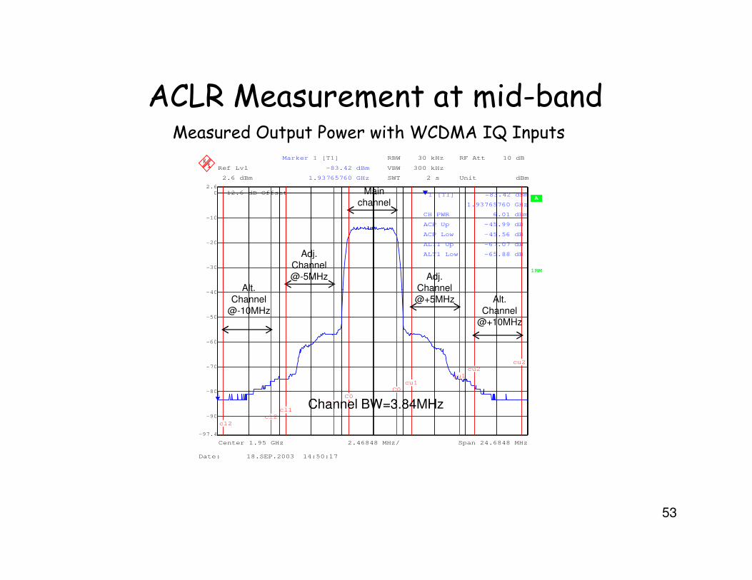
ACLR Measurement at mid-band
Ref Lvl
2.6 dBm
Ref Lvl
2.6 dBm
RBW 30 kHz
VBW 300 kHz
SWT 2 s
RF Att 10 dB
A
1RM
Unit dBm
12.6 dB Offset
-40
-30
-20
-10
0
2.6
Marker 1 [T1]
-83.42 dBm
1.93765760 GHz
1 [T1] -83.42 dBm
1.93765760 GHz
CH PWR 6.01 dBm
ACP Up -45.99 dB
ACP Low -45.56 dB
ALT1 Up -67.07 dB
ALT1 Low -65.88 dB
Measured Output Power with WCDMA IQ Inputs
Main
channel
Adj.
Channel
@-5MHz Adj.
ChannelAlt.
53
2.46848 MHz/Center 1.95 GHz Span 24.6848 MHz
-90
-80
-70
-60
-50
-40
-97.4
1
cl2
cl2
cl1
cl1
C0
C0
cu1
cu1
cu2
cu2
Date: 18.SEP.2003 14:50:17
Channel
@+5MHz
Alt.
Channel
@-10MHz
Alt.
Channel
@+10MHz
Channel BW=3.84MHz
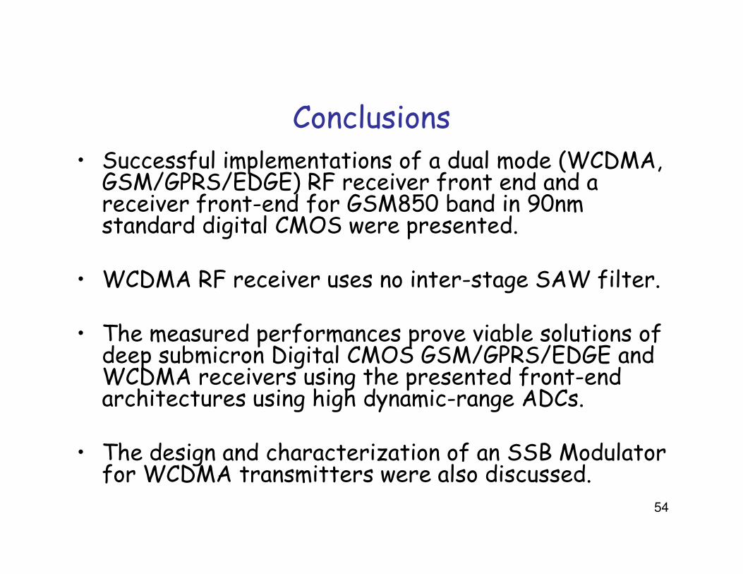
Conclusions• Successful implementations of a dual mode (WCDMA,
GSM/GPRS/EDGE) RF receiver front end and a receiver front-end for GSM850 band in 90nm standard digital CMOS were presented.
• WCDMA RF receiver uses no inter-stage SAW filter.
54
• WCDMA RF receiver uses no inter-stage SAW filter.
• The measured performances prove viable solutions of deep submicron Digital CMOS GSM/GPRS/EDGE and WCDMA receivers using the presented front-end architectures using high dynamic-range ADCs.
• The design and characterization of an SSB Modulator for WCDMA transmitters were also discussed.
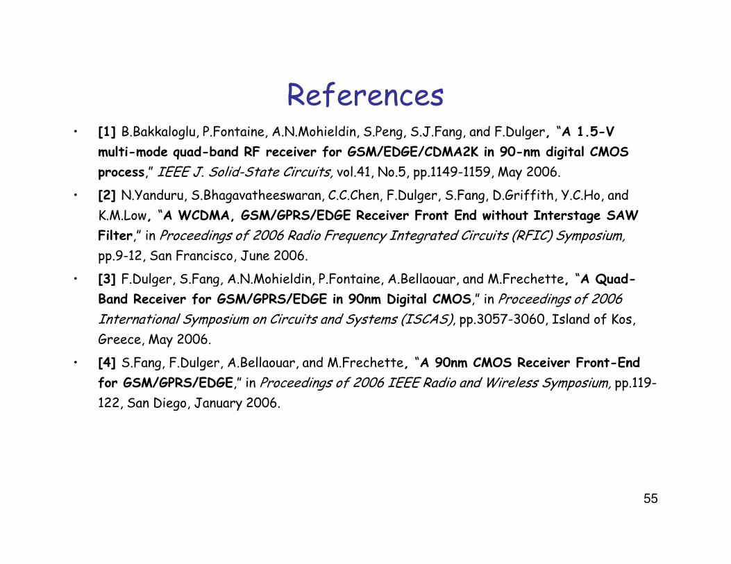
References• [1] B.Bakkaloglu, P.Fontaine, A.N.Mohieldin, S.Peng, S.J.Fang, and F.Dulger, “A 1.5-V
multi-mode quad-band RF receiver for GSM/EDGE/CDMA2K in 90-nm digital CMOS
process,” IEEE J. Solid-State Circuits, vol.41, No.5, pp.1149-1159, May 2006.
• [2] N.Yanduru, S.Bhagavatheeswaran, C.C.Chen, F.Dulger, S.Fang, D.Griffith, Y.C.Ho, and
K.M.Low, “A WCDMA, GSM/GPRS/EDGE Receiver Front End without Interstage SAW
Filter,” in Proceedings of 2006 Radio Frequency Integrated Circuits (RFIC) Symposium,
pp.9-12, San Francisco, June 2006.
• [3] F.Dulger, S.Fang, A.N.Mohieldin, P.Fontaine, A.Bellaouar, and M.Frechette, “A Quad-
55
• [3] F.Dulger, S.Fang, A.N.Mohieldin, P.Fontaine, A.Bellaouar, and M.Frechette, “A Quad-
Band Receiver for GSM/GPRS/EDGE in 90nm Digital CMOS,” in Proceedings of 2006
International Symposium on Circuits and Systems (ISCAS), pp.3057-3060, Island of Kos,
Greece, May 2006.
• [4] S.Fang, F.Dulger, A.Bellaouar, and M.Frechette, “A 90nm CMOS Receiver Front-End
for GSM/GPRS/EDGE,” in Proceedings of 2006 IEEE Radio and Wireless Symposium, pp.119-
122, San Diego, January 2006.
Acknowledgements
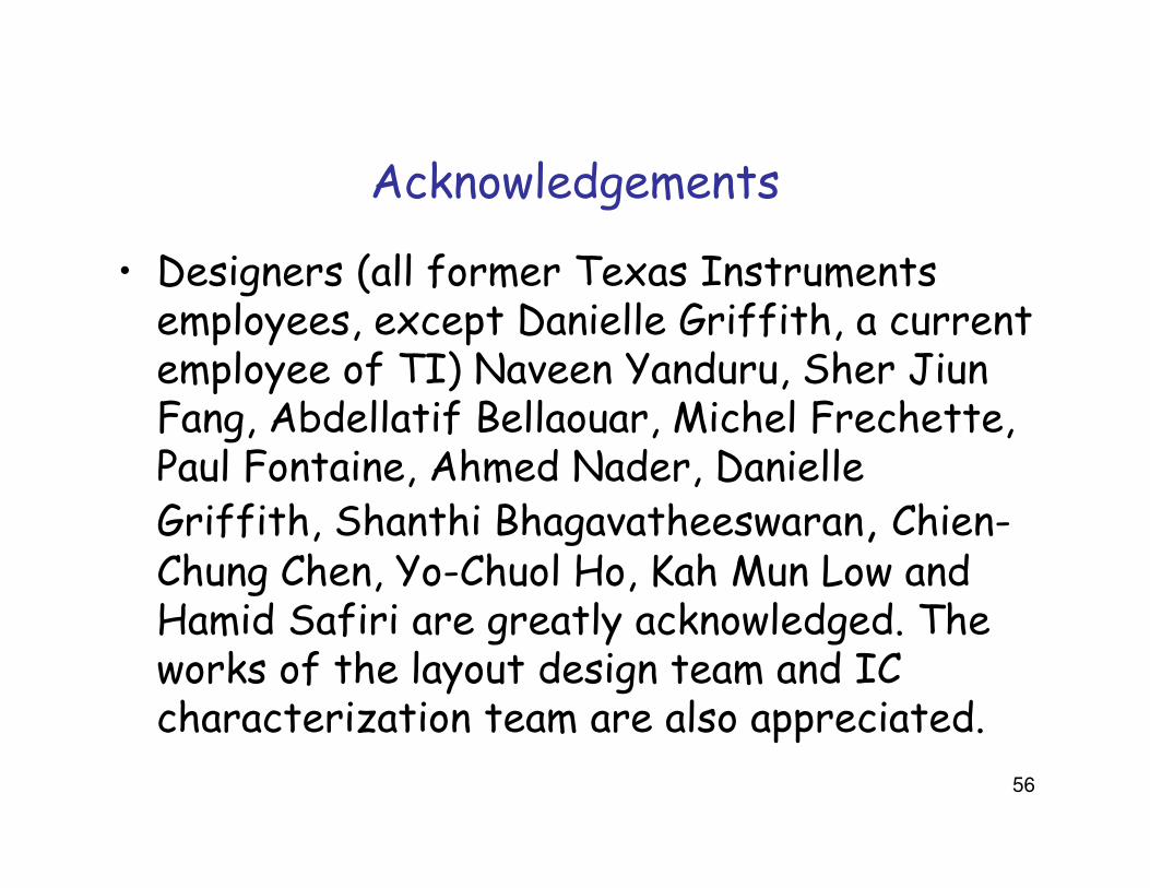
• Designers (all former Texas Instruments employees, except Danielle Griffith, a current employee of TI) Naveen Yanduru, Sher JiunFang, Abdellatif Bellaouar, Michel Frechette, Paul Fontaine, Ahmed Nader, Danielle
56
Paul Fontaine, Ahmed Nader, Danielle Griffith, Shanthi Bhagavatheeswaran, Chien-Chung Chen, Yo-Chuol Ho, Kah Mun Low and Hamid Safiri are greatly acknowledged. The works of the layout design team and IC characterization team are also appreciated.
VAAO~AJ m~:;//3101 A/r' ~h vJ.p- ~X;L T' IV
v C D ~~/' :f &-~_~~ (
(J fA ~ 11-(yj tW7.-~ -;Lv ~ez..L~ ~
;J) ; .e-t"L~ G:-fi ~ ~ !Jc5 flp.J if 5 IY) .s A.t~~
LN4 ~~ ~~ /.?-f
fJiJr~ ~~~ l AIIt _ I ,,- eiJ.
r1uf. ~-~ C Mv-s Cf{) m~
C~lIJ'Pc- J DC5 ~
.~::J \~ ~ ~ IV c;. D 1'1 ~ _ '15 t-/f." -) 11 ~ L~- :? ~ /1", £/
~~LNA-<) ,5 /'vII l+g w'e- OJvI0! ret: 1-/lY+- ,
'3 WJr I-I ""(.,
~ <' Jv', ~ 'I
1
Jim Gunn
From: [email protected] on behalf of Judah Mordecai Epstein [[email protected]]
Sent: Sunday, May 17, 2009 12:22 AMTo: [email protected]: IEEE/CVT - *May Luncheon Meeting - 5/19/09*
THE INSTITUTE OF ELECTRICAL AND ELECTRONICS ENGINEERS, INC. COMMUNICATIONS & VEHICULAR TECHNOLOGY SOCIETIES 2009 TECHNICAL LUNCHEON PROGRAM Technical Presentation: RF IC Design for Cellular Transceiver Front-Ends on Silicon - Fikret DÜLGER, Senior RF IC Design Engineer, Microtune Inc. Networking Presentation: Insider Tips from a Recruiter's perspective on Job Searching in 2009 - Patty Martin, Senior Technical Recruiter, HumCap, LLP Addison, TX DATE: Tuesday 19 May 2009 TIME: Luncheon starts at 11:00 a.m. Main Presentation is from 12:00-1:00p.m. PLACE: Holiday Inn Select, 1655 N. Central, Richardson Please call 972 238 1900 for directions (SW Corner Campbell and Central) COST: $5 for IEEE Members, $10 for Non-Members No charge for Student and Life Members Abstract: Deep submicron Digital CMOS technology has become the technology of choice in Radio Frequency IC implementations for multi-band, multi-mode Cellular Systems owing to its lower cost due to the possibility of integration with the digital circuitry (DSP, memory, etc.) on the same die and to its ease of programmability. This choice is making the design of RF front-end building blocks of transceivers challenging. In the first part of
2
this talk, some of these challenges will be pointed out and addressed within the context of two Receiver Front-Ends designed in 90nm Digital CMOS. The first design is a GSM/GPRS/EDGE (GGE) receiver front-end for GSM850 Band. With a low power of 46mW, it achieves 31dB gain, 2.1dB integrated noise figure, 5dB of noise figure under blocking condition and -9.5dBm of in-band IIP3. The second design example is a Dual Mode Receiver for DCS Band. It uses direct conversion for WCDMA mode and 100 kHz low IF for GGE mode. No inter-stage SAW filter is used between the LNA and the mixer. The receiver has a NF of 2.9dB and meets all the out of band and in-band linearity requirements for both WCDMA and GGE modes. In the second part of the presentation, the design and characterization of an important building block in a W-CDMA transmitter, the Single-Sideband (SSB) Modulator will be treated. The performance of the SSB Modulator has an important effect on both the linearity and noise of the transmitter. The high degree of amplitude variation in the W-CDMA signals requires very high linearity in the transceivers. Another important challenge is the TX noise at the receive band due to the full FDD (frequency-division duplex) nature of the transceiver, meaning both the TX and the RX are on at the same time. Some measurement results associated with the SSB modulator of a W-CDMA transceiver designed and implemented in a 0.18μm SiGe BiCMOS technology will conclude the talk. Bio: Fikret Dülger received the B.S. and M.S. degrees in electronics from Istanbul Technical University (ITU), Istanbul, Turkey, in 1993 and 1996, respectively, and the Ph.D. degree in electronics from Texas A&M University, College Station, in 2002. He was a Research Assistant with the Electronics and Communication Engineering Department, Istanbul Technical University, from 1993 to 1996. In 1994, he was a Design Engineer with the ETA ASIC Design Center, Istanbul, developing full-custom mixed-mode industrial ASICs. In the 1998 and 1999 summer terms, he worked in the RF IC Design Group, Texas Instruments Incorporated, Dallas, TX, as a Design Engineer for his internships. He was a graduate student and Research and Teaching Assistant in the Department of Electrical Engineering, Texas A&M University, between Fall 1996 and Spring 2002. From January 2002 to February 2009, he worked as a Design Engineer in the RF IC Design Group, Texas Instruments Inc.. He is currently a Senior RF IC Design Engineer with Microtune Inc., Plano, TX. In addition to being coauthor of numerous scientific papers in international journals and conferences, he is coauthor of a book titled Integrated RF Building Blocks for Wireless Communication Transceivers (Saarbrucken, VDM Verlag Dr. Mueller, 2008) based on his doctoral dissertation. His research and professional interests are in the area of analog circuit design for RF integrated circuits. _______________________________________________________________ Networking Presentation: Abstract: Executing a successful job search in 2009 is a different process than in years past - gone are the days of posting your resume on Monster or CareerBuilder and sitting back to wait
3
for the calls to roll in. The economy of 2009 has affected all facets of daily life including how to find a job. This presentation will give the job seeker insider tips on how a recruiter views you as a potential candidate and how you might make that view more successful. Today’s jobseeker is competing with thousand of well-qualified candidates for the same position. This presentation will help you:
• Prepare a better resume • Utilize on-line tools to facilitate your job search • Make recruiters want to help you find a job
Bio:
Patty Martin is a Sr. Technical Recruiter at HumCap and specializes in identifying and recruiting hard-to-find passive candidates with specific emphasis in Supply Chain, Engineering and IT positions. She has had success at HumCap recruiting and placing high level candidates both locally and in international locations. Before joining HumCap, Patty was a Sr. Research Associate at TNS Partners, a Dallas-based executive level retained search firm. Her experience includes recruiting in multiple industries; such as Information Technology, A/E/C Engineering, Energy and Finance/Accounting. Within these industries, Patty has recruited for all levels of positions, with major focus on manager and executive level positions.
Prior to entering the field of executive search, Patty was a successful Supply Chain Consultant and ERP salesperson, selling high end software and consulting services to Fortune 1000 manufacturing companies around the globe. Her 10 year’s experience as a Manufacturing Manager especially equipped her to provide first hand knowledge to the issues faced by clients related to issues of optimizing the supply chain, reducing inventory and implementing Lean Manufacturing. Her complete profile may be viewed at http://www.linkedin.com/in/pattymartin
View a listing of all current engineering openings.
16301 B Quorum Drive, Suite 100 | Addison, Texas 75001 214.520.0760 | Toll Free: 877.244.5723 | Fax 214.520.8839 Dallas Business Journal: Top 10 Recruiting Firms - 2005 & 2006, Best Places to Work - 2006 & 2007 Inc. Magazine: Fastest Growing Private Companies - 2007