RF subsystem power consumption and induced radiation...
155
General rights Copyright and moral rights for the publications made accessible in the public portal are retained by the authors and/or other copyright owners and it is a condition of accessing publications that users recognise and abide by the legal requirements associated with these rights. • Users may download and print one copy of any publication from the public portal for the purpose of private study or research. • You may not further distribute the material or use it for any profit-making activity or commercial gain • You may freely distribute the URL identifying the publication in the public portal If you believe that this document breaches copyright please contact us providing details, and we will remove access to the work immediately and investigate your claim. Downloaded from orbit.dtu.dk on: Jun 21, 2018 RF subsystem power consumption and induced radiation emulation Musiige, Deogratius; Anton, François; Mioc, Darka Publication date: 2013 Document Version Publisher's PDF, also known as Version of record Link back to DTU Orbit Citation (APA): Musiige, D., Anton, F., & Mioc, D. (2013). RF subsystem power consumption and induced radiation emulation. Kgs. Lyngby: Technical University of Denmark (DTU). (PHD-2013; No. 304).
Transcript of RF subsystem power consumption and induced radiation...

General rights Copyright and moral rights for the publications made accessible in the public portal are retained by the authors and/or other copyright owners and it is a condition of accessing publications that users recognise and abide by the legal requirements associated with these rights.
• Users may download and print one copy of any publication from the public portal for the purpose of private study or research. • You may not further distribute the material or use it for any profit-making activity or commercial gain • You may freely distribute the URL identifying the publication in the public portal
If you believe that this document breaches copyright please contact us providing details, and we will remove access to the work immediately and investigate your claim.
Downloaded from orbit.dtu.dk on: Jun 21, 2018
RF subsystem power consumption and induced radiation emulation
Musiige, Deogratius; Anton, François; Mioc, Darka
Publication date:2013
Document VersionPublisher's PDF, also known as Version of record
Link back to DTU Orbit
Citation (APA):Musiige, D., Anton, F., & Mioc, D. (2013). RF subsystem power consumption and induced radiation emulation.Kgs. Lyngby: Technical University of Denmark (DTU). (PHD-2013; No. 304).

RF subsytem power consumptionand induced radiation emulation
Deogratius Musiige
Kongens Lyngby 2013DTU space-PhD-2013-304

Technical University of DenmarkNational Space InstituteElektrovej, building 327+328 andØrsteds Plads, building 348 DK-2800 Kgs. LyngbyPhone +45 45259730,Fax +45 [email protected] DTU space-PhD-2013-304

Summary
The thesis introduces a novel approach towards the emulation of the RF subsys-tem power consumption when transmitting a LTE signal. The RF subsystemwhich is made up of analog components has not been covered by the status quoemulation methodologies which are compatible with digital circuits. Thoughthe study of the RF subsystem architectures revealed numerous architectureswith different impacts on power consumption, we have decided to consider theRF subsystem as a black box.
The RF subsystem power emulation has been studied for the telecommunica-tion technology Long Term Evolusion (LTE). Given the fact that major powerconsumptions of wireless devices are largely functions of sequences of proto-col/logical activities, it is this technology that provided the inputs to the RFsubsystem as a black black box which are Tx power, carrier frequency and signalbandwidth. The physical environmental variable temperature has also provento be very influential on power consumption. These inputs also do constitute tothe input parameters of the emulation methodology.
The emulation methodology has been proven to be a mathematical mappingbetween the input parameters and a predefined mathematical model. For themathematical model, multivariate modeling approaches were analyzed for anapproach with the least modeling error and complexity. Herein, the homotopycontinuation numerical approach proved to have the least modeling error of 3%.The RF subsystem power consumption has been emulated with accuracies of84% ±2.25% and 94.3% ±2.25% on different devices.

ii

Resume
Denne afhandling introducerer en ny tilgang til emulering af RF subsystemetsstrømforbrug. RF subsystemet, som består af analoge komponenter, er ikke ble-vet dækket af nuværende emulerings metoder, der er kompatible med digitalekredsløber. Selvom evalueringen af RF subsystemers arkitekturer afslørede ad-skillige arkitekturer med forskellige virkninger på strømforbrug, har vi besluttetat betragte RF subsystemet som en sort boks.
Emuleringen af RF subsystemets strømforbrug er blevet undersøgt for telekom-munikationsteknologi “Long Term Evolusion (LTE)”. I betragtning af at de storestrømforbruge af trådløse enheder er stort set funktioner af sekvenser af protokol/logiske aktiviteter, det er denne teknologi, der fastsat input til RF subsystemet.Disse input er transmissionsstyrke, frekvens og signal båndbredde og det fysiskemiljø variable temperatur som også har vist sig til at have en stor indflydelsepå strømforbruget. Disse input udgør også de input parametre til emuleringmetodologien.
Emulering metodologien har vist sig at være en matematisk mapping melleminput parametre og et foruddefineret matematisk model. For at finde matema-tiske modelet, blev multivariabel modelleringsmetoder analyseret for en modelmed mindste modellering fejl og kompleksitet. Heri “homotopy continuation”numeriske tilgang viste sig at have den mindste modellering fejl på 3%. RF sub-systemets strømforbrug er blevet emuleret med nøjagtigheder af 84% ±2.25%og 94% ±2.25% på forskellige enheder.

iv

Preface
This thesis was prepared at the National Space Institute of the Technical Uni-versity of Denmark in fulfilment of the requirements for acquiring the degree ofDoctor of Philosophy.
The thesis deals with the emulation of the RF subsystem power consumption.The thesis also looked into the possibilities of emulating the induced SAR whenusing the wireless devices close to our bodies. The experimental part of thisresearch have been mainly conducted at the Renesas Mobile Europe site whereall power measurements related to the thesis where conducted in the SW labora-tory. The microwave laboratory of the Colorado University at Boulder was usedfor the radiation studies. This research was funded by Nokia/Renesas MobileEurope, The Danish Ministry for Innovation and an industrial Ph.D scholarship.
The thesis presents the summary of the research conducted in five chapters. Theintroductory part consists of the introduction to the problem and the conceptsand the status quo over the previously applied approaches. The rest of the thesissummaries our published work on the approaches applied for solving the taskin this research.
The industrial supervision of the research has been conducted by Vincent Laulagnetand the academic supervision by Francois Anton, and Darka Mioc of The DanishSpace Institute at the Technical University of Denmark.

vi
Lyngby, 30-June-2013
Deogratius Musiige

Publications
Shortlisted below are the patents and scientific publications (journal and confer-ence papers) made during the course of this work. All the publications directlyconcerned with the problem at task.
Patents
• METHOD AND APPARATUS FOR PROVIDING A DYNAMIC PAG-ING PERIOD(Link), Europe PCT/IB2009/052039
• Methods, devices and computer program products providing for establish-ing a model for emulating a physical quantity which depends on at leastone input parameter, and use thereof(Link), United States 20130013270
Journal papers:
• D. Musiige, F. Anton, V. Yatskevich, L. Vincent, D. Mioc, and N. Pierre,“Rf power consumption emulation optimized with interval valued homo-topies,” World Academy of Science, Engineering and Technology 81 2011,vol. 81, pp. 147-153, Sep 2011.(Published)
• D. Musiige, F. Anton, V. Laulagnet, Florin Apetri and Darka Mioc “LTERF subsystem power consumption modeling,” : IEEE Transactions onVery Large Scale Integration Systems 2013 (Under review)

viii
Conference papers (all published)
• Deogratius Musiige, Laulagnet Vincent, Francois Anton, Darka Mioc “Ltehandset rf power consumption emulation,” in The Third InternationalConference on Digital Information Processing and Communications, Febru-ary 2013, pp. 371-378.
• D. Musiige, V. Laulagnet, and F. Anton, “LTE RF subsystem power con-sumption modeling,” in The 1st IEEE Global Conference on ConsumerElectronics 2012 (IEEE GCCE 2012), Tokyo, Japan, Oct. 2012.
• D. Musiige, L. Vincent, and F. Anton, “Lte modem power consumption, sarand rf signal strength emulation,” in Ultra Modern Telecommunicationsand Control Systems and Workshops (ICUMT), 2012 4th InternationalCongress on, 2012, pp. 1-6.

Acknowledgements
Praise be to God for providing me with the gift of life and the intellect to reachthis academic stage.
My greatest gratitude to Vincent Laulagnet and Francois Anton my main super-visors, for proposing the project and pursuing the application processes throughNokia, DTU and the Danish Ministry of Innovation. The whole supervisoryteam which also included Darka Mioc, the co-supervisor, have done a great jobin guiding, supervising and motivating during the whole coarse of this project.I do appreciate all of your work that you have invested in me.
My colleagues at Renesas, without spelling any names, you have been veryhelpful in my research with your guidance especially for the practical stuffs inthe SW Laboratory. And a special thanks to the colleagues who reviewed mywork and attended my talks.
Lastly my family, my parents who put me on the right path from day oneand taught me always to pursue for the highest. My siblings who have alwaysbeen there as my biggest motivator and my friends, especially Muhan who havealways peep talked me through hard times. I want to say thank you. And myone and only, thanks for enduring my long working hours and the support.

x

Contents
Summary i
Resume iii
Preface v
Publications vii
Acknowledgements ix
1 Introduction 11.0.1 Synopsis . . . . . . . . . . . . . . . . . . . . . . . . . . . . 7
2 Overview 92.1 RF subsystem architecture overview . . . . . . . . . . . . . . . . 9
2.1.1 Introduction . . . . . . . . . . . . . . . . . . . . . . . . . 92.1.2 RF architectures . . . . . . . . . . . . . . . . . . . . . . . 102.1.3 Current trends for LTE transmitters . . . . . . . . . . . . 172.1.4 Future trends . . . . . . . . . . . . . . . . . . . . . . . . . 182.1.5 Summary . . . . . . . . . . . . . . . . . . . . . . . . . . . 18
2.2 LTE Review . . . . . . . . . . . . . . . . . . . . . . . . . . . . . . 192.2.1 Introduction . . . . . . . . . . . . . . . . . . . . . . . . . 192.2.2 The LTE structure . . . . . . . . . . . . . . . . . . . . . . 202.2.3 Emulation realization of the LTE structure . . . . . . . . 222.2.4 The LTE technologies . . . . . . . . . . . . . . . . . . . . 222.2.5 LTE future trends . . . . . . . . . . . . . . . . . . . . . . 302.2.6 LTE structural and technological influence on radiation
and power consumption . . . . . . . . . . . . . . . . . . . 312.2.7 Summary . . . . . . . . . . . . . . . . . . . . . . . . . . . 32

xii CONTENTS
2.3 Power consumption estimation overview . . . . . . . . . . . . . . 322.3.1 Analytical power consumption estimating methodology . 342.3.2 Empirical power consumption estimating methodology . . 362.3.3 Power consumption emulation . . . . . . . . . . . . . . . . 392.3.4 Summary . . . . . . . . . . . . . . . . . . . . . . . . . . . 41
2.4 Electromagnetic radiation . . . . . . . . . . . . . . . . . . . . . . 412.4.1 SAR and MPE . . . . . . . . . . . . . . . . . . . . . . . . 41
2.5 Summary . . . . . . . . . . . . . . . . . . . . . . . . . . . . . . . 44
3 RF subsystem power measurements 453.1 Introduction . . . . . . . . . . . . . . . . . . . . . . . . . . . . . . 453.2 The power measurement Setup and procedure . . . . . . . . . . . 46
3.2.1 The Hardware . . . . . . . . . . . . . . . . . . . . . . . . 463.2.2 Instruments calibration . . . . . . . . . . . . . . . . . . . 473.2.3 SW configuration . . . . . . . . . . . . . . . . . . . . . . . 473.2.4 Measurement procedure . . . . . . . . . . . . . . . . . . . 483.2.5 Power consumption uncertainty/precision . . . . . . . . . 493.2.6 Evaluation of the measurement system and methodology . 50
3.3 Summary . . . . . . . . . . . . . . . . . . . . . . . . . . . . . . . 50
4 LTE RF subsystem power consumption modeling 574.1 Introduction . . . . . . . . . . . . . . . . . . . . . . . . . . . . . . 574.2 Overview . . . . . . . . . . . . . . . . . . . . . . . . . . . . . . . 58
4.2.1 RF subsystem power consumption emulation . . . . . . . 584.3 FLPA analysis of the RF subsystem . . . . . . . . . . . . . . . . 59
4.3.1 Primary Functional Analysis . . . . . . . . . . . . . . . . 594.3.2 Device power profiling . . . . . . . . . . . . . . . . . . . . 604.3.3 The power consumption modeling . . . . . . . . . . . . . 694.3.4 Evaluation of the RF subsystem Power modeling approaches 76
4.4 Discussion . . . . . . . . . . . . . . . . . . . . . . . . . . . . . . . 864.5 Summary . . . . . . . . . . . . . . . . . . . . . . . . . . . . . . . 86
5 LTE handset RF power consumption emulation 875.1 Introduction . . . . . . . . . . . . . . . . . . . . . . . . . . . . . . 875.2 Power emulation model . . . . . . . . . . . . . . . . . . . . . . . 90
5.2.1 RF subsystem Power consumption emulation . . . . . . . 905.3 Integration into the power management flow . . . . . . . . . . . . 97
5.3.1 Extrapolation to field measurements . . . . . . . . . . . . 985.3.2 Power consumption optimization . . . . . . . . . . . . . . 99
5.4 Discussion . . . . . . . . . . . . . . . . . . . . . . . . . . . . . . . 99

CONTENTS xiii
6 Conclusions 1036.0.1 Introduction . . . . . . . . . . . . . . . . . . . . . . . . . 1036.0.2 Problem domain . . . . . . . . . . . . . . . . . . . . . . . 1036.0.3 Results of the research . . . . . . . . . . . . . . . . . . . . 1046.0.4 Future work . . . . . . . . . . . . . . . . . . . . . . . . . . 105
A Appendix 107A.0.5 CMOS WCDMA transmitter performances . . . . . . . . 107A.0.6 BiCMOS WCDMA transmitters . . . . . . . . . . . . . . 109A.0.7 Architectural power efficiency comparison . . . . . . . . . 110A.0.8 Architectural performance evaluation . . . . . . . . . . . . 111
A.1 LTE review appendix . . . . . . . . . . . . . . . . . . . . . . . . . 111A.1.1 The orthogonality principle . . . . . . . . . . . . . . . . . 111A.1.2 The relationship between the geometric envelop and the
back-off requirement. . . . . . . . . . . . . . . . . . . . . . 113A.1.3 The full LTE structure . . . . . . . . . . . . . . . . . . . . 113
Bibliography 121

xiv CONTENTS

List of Figures
1.1 The wireless modem whose power consumption is emulated inthis work . . . . . . . . . . . . . . . . . . . . . . . . . . . . . . . 2
1.2 Modem power consumption distribution . . . . . . . . . . . . . . 31.3 Visualization of SAR . . . . . . . . . . . . . . . . . . . . . . . . . 6
2.1 Typical RF topology . . . . . . . . . . . . . . . . . . . . . . . . . 102.2 Direct up conversion topology . . . . . . . . . . . . . . . . . . . . 112.3 Offset and 2 step architectures . . . . . . . . . . . . . . . . . . . 122.4 Offset PLL architecture designs . . . . . . . . . . . . . . . . . . . 132.5 LINC architecture . . . . . . . . . . . . . . . . . . . . . . . . . . 142.6 Polar transmitter . . . . . . . . . . . . . . . . . . . . . . . . . . . 152.7 Polar transmitter with fractional-N PLL . . . . . . . . . . . . . . 152.8 The LTE E-UTRAN structure . . . . . . . . . . . . . . . . . . . 212.9 The FDM modulation . . . . . . . . . . . . . . . . . . . . . . . . 232.10 The OFDM modulation . . . . . . . . . . . . . . . . . . . . . . . 242.11 OFDM employing TDMA . . . . . . . . . . . . . . . . . . . . . . 242.12 OFDM transmitter . . . . . . . . . . . . . . . . . . . . . . . . . . 262.13 OFDMA allocation . . . . . . . . . . . . . . . . . . . . . . . . . . 262.14 TDD (Time-Division Duplex) . . . . . . . . . . . . . . . . . . . . 282.15 FDD (Frequency Division Duplex) . . . . . . . . . . . . . . . . . 292.16 MIMO . . . . . . . . . . . . . . . . . . . . . . . . . . . . . . . . . 302.17 SOC design levels of abstraction . . . . . . . . . . . . . . . . . . 332.18 The top-down and bottom-up approaches . . . . . . . . . . . . . 352.19 The system level power model . . . . . . . . . . . . . . . . . . . . 372.20 The analog component model . . . . . . . . . . . . . . . . . . . . 382.21 Power emulation of digital circuits at the RTL level of abstraction 402.22 The handset held with a robot arm . . . . . . . . . . . . . . . . . 44

xvi LIST OF FIGURES
3.1 Power measurement setup . . . . . . . . . . . . . . . . . . . . . . 513.2 Calibration of the measurement resistor . . . . . . . . . . . . . . 523.3 The RF GUI . . . . . . . . . . . . . . . . . . . . . . . . . . . . . 523.4 The setup for automated power measurements . . . . . . . . . . 533.5 The precision in the measurement process . . . . . . . . . . . . . 533.5 The distributions of power consumption at ambient temperatures 553.6 The buffer zones of three independent measurements . . . . . . . 56
4.1 Power consumption as a function of carrier frequency . . . . . . . 624.2 Device profiling combinations . . . . . . . . . . . . . . . . . . . . 634.3 Power consumption as function of temperature continued on the
next page... . . . . . . . . . . . . . . . . . . . . . . . . . . . . . . 654.3 The influence of temperature on power consumption for signal
bandwidths . . . . . . . . . . . . . . . . . . . . . . . . . . . . . . 664.4 Power consumption as a function of frequency measured at am-
bient temperatures . . . . . . . . . . . . . . . . . . . . . . . . . . 674.5 Physical measurement setup . . . . . . . . . . . . . . . . . . . . . 684.6 Network diagram for the two layer neural network . . . . . . . . 724.7 The performance of multivariate polynomial fitting . . . . . . . . 784.8 The convergence of non-linear optimization algorithms . . . . . . 794.9 Homotopy based modeling continued on next page... . . . . . . . 824.9 The homotopy based modeling of the power consumption . . . . 834.10 Bivariate homotopy functions . . . . . . . . . . . . . . . . . . . . 844.11 Evaluation of the homotopy approach . . . . . . . . . . . . . . . 85
5.1 The RF subsystem power emulation system . . . . . . . . . . . . 885.2 Emulation flow . . . . . . . . . . . . . . . . . . . . . . . . . . . . 895.3 The power emulation validation setup using a system simulator . 915.4 The requested and measured Tx power for local and normal modes 935.5 The measured and emulated power consumption . . . . . . . . . 945.6 The expected emulation system accuracies . . . . . . . . . . . . . 955.7 Emulation validation using a device from the early stage of the
product development . . . . . . . . . . . . . . . . . . . . . . . . . 965.8 The power management flow . . . . . . . . . . . . . . . . . . . . 1005.9 Emulated power of the DUT during a FTP upload . . . . . . . . 101
A.1 The orthogonality principle . . . . . . . . . . . . . . . . . . . . . 112A.2 Envelop Vs. PA efficiency . . . . . . . . . . . . . . . . . . . . . . 113A.3 LTE structure . . . . . . . . . . . . . . . . . . . . . . . . . . . . . 114A.4 Downlink mapping . . . . . . . . . . . . . . . . . . . . . . . . . . 119A.5 Uplink map . . . . . . . . . . . . . . . . . . . . . . . . . . . . . . 119

xvii

xviii Contents

List of Tables
2.1 SAR . . . . . . . . . . . . . . . . . . . . . . . . . . . . . . . . . . 422.2 MPE . . . . . . . . . . . . . . . . . . . . . . . . . . . . . . . . . . 422.3 Simulated Vs. measured SAR . . . . . . . . . . . . . . . . . . . . 43
3.1 Calibration values of the measurement resistor . . . . . . . . . . 47
4.1 LTE technological high level parameters’ lower and higher bounds 614.2 The device power profiling . . . . . . . . . . . . . . . . . . . . . . 614.3 Validation error for the optimization algorithms . . . . . . . . . . 80
A.1 CMOS WCDMA transmitters . . . . . . . . . . . . . . . . . . . . 108A.2 BiCMOS transmitters . . . . . . . . . . . . . . . . . . . . . . . . 109A.3 The transmitters power efficiency . . . . . . . . . . . . . . . . . . 110A.4 Transmitter achitectural comparison . . . . . . . . . . . . . . . . 111

xx LIST OF TABLES

Chapter 1
Introduction
Wireless devices as cellular phones, portable and mobile devices have becomean integral part of our daily lives. The complexity of our expectations for thesedevices is also on a rampage. We are expecting these devices to provide cellular,high data rates and GPS connections on top of elegant, smart and slim designs.Our dependence on these gadgets makes a “wishing-full thinking” requirementthat they can operate indefinitely on a single charge of the battery or realisticallya single charge a day.
On the other hand, electromagnetic exposure regulatory bodies are tighteningon the allowable electromagnetic radiation. The demand for slim and tenderdevices makes this very challenging as the users are increasingly exposed toelectromagnetic radiation as the distance between the radiating devices andusers’ bodies shrink [1].
From a wireless modem chipset point of view, the target is to apply technologiesthat would achieve the highest possible data rates at a minimal productionprice and power consumption per throughput bit. Sophisticated modulationand access schemes, such as OFDMA and SC-FDMA in LTE [2] down-link anduplink respectively, have been introduced to increase capacity and meet the highdata rate demands.
However, in terms of minimal production price and power consumption per

2 Introduction
11
DBB IC
Cellular Domain(WGEM +
Cortex-R4x2 )
Mini-HostDomain
DRAM
Modem side
DigRF v4
AudioDomain APE
DR
AM
APE side
Buffer
for
Celluar
Buffer
for
Min
i-H
ost
SB
SC
DM
A
SH
wy
C2C
IPC
DRAM
Buffer
for
Celluar
Buffer
for
Min
i-H
ost
SB
SC
Di
RFIC
HP
A
RF F
EM
Figure 1.1: The wireless modem whose power consumption is emulated in thiswork. The modem consists of two main modules, the Digital BaseBand Integrated Circuit (DBB IC) and the RF subsystem madeup of the RFIC (Radio Frequency Integrated Circuit), HPA (HighPower Amplifier) and RF FEM (Front End Modules).
throughput bit for a wireless handset, the low cost and low power consumptioncriteria are heavily influenced by both the baseband (BB) and radio-frequency(RF) components [3] of the modem shown in Figure 1.1. This is stated withrespect to the double and quad core application processors applied in today’ssmart-phones because seen over 24 hours, the modem would be active for everygiven paging period of around a second. A power consumption analysis of asmartphone [4] showed that the modem consumes on average 80.6% and 59%of the total smartphone power (excluding the blacklight) for a GSM phone calland General Packet Radio Service (GPRS) emailing, respectively. In the uplinkdirection, measurements conducted in this work show the RF subsystem asthe worst power consumer as a function of the transmission power (Tx power).Figure 1.2 shows the distribution of the power consumption among modemmodules when transmitting at Tx powers of 0dBm and 23dBm where the RFsubsystem (RFIC and PA) consumes 61% and 86% of the total modem powerconsumption.
It is of interest for modem chipset developers to be able to predict the averagepower consumption when transmitting a LTE signal, at sub-frame resolution,of the wireless modem during the design process as it relates to the differentcomponents. In this work our main focus is the RF subsystem which is the mainpower consumer in the modem however, approaches towards the extension ofthe methodology to the whole modem will be taken. Our intention is to havepredictions that do reflect realistic scenarios, for example uploading data while

3
RF 57%
PA 4%
DBB 32%
Other 7%
(a) Max throughput at 0 dBm,
RF 28%
PA 58%
DBB 12%
Other 3%
(b) Max throughput at 23 dBm,
Figure 1.2: Modem power consumption distribution during a max throught-put scenario at 0 and 23 dBm transmition powers of a RenesasMobile Europe modem in development. The RF power consti-tutes the RF FEM and RFIC and PA is the power amplifier.
,

4 Introduction
driving through a metropolitan area or while sitting in a fast moving train.Scenarios where the device is challenged by the highly alternating transmissionpower requests (from the base-station) and carrier frequencies as the devicemoves from/to various base-stations. According to Friis Transmission Equation[5],
Pr
Pt=
(λ
4πR
)2
G0tG0r
where Pr and Pt are the received and transmitted powers, λ the wave length,R the distance between the transmitter and receiver, G0t and G0r are the max-imum gains for transmitter and receiver antennas,
the transmitted power would at least be attenuated by 1R2 for at distance R be-
tween the transmitting device and the base-station while not considering all theother interferences that do exist in the transmission path. The carrier frequen-cies will change as the device also pursues to connect to a stronger signal as it isdriven through various cells. Hence, in the pursuit for designing power efficientdevices, it’s absolutely vital to be able to estimate the power consumption ofthe wireless modem in these worst case realistic scenarios.
A formal method for achieving this prediction is referred to as emulation. Incontrast to simulation predictions, in the emulation approach some functionalparts of the emulation system have to be carried out by the targeted real sys-tem [6]. Power emulation approaches for the digital circuits, as in the digitalbaseband in modem, have been publicized and commercialized at the RTL (Reg-ister Transfer Level) and gate levels. Extensive work has been published on theestimation of power consumption for SoC (System-on-Chip) systems at variouslevels of abstraction [7–10]. Figure 2.18 shows the levels of abstraction duringthe design of SoC systems. We can observe that the amount of informationincreases by an order of magnitude as the design maneuvers from system levelto transistor level [11]. Consequently, the accuracy of power consumption esti-mation also increases as more knowledge is gained when the design transversesfrom the system level to the transistor level.
Approaches for power estimation at the RTL level of abstraction have beencommercialized into power estimating tools [12–17]. The applicability of thePowerTheater [15], SpyGlass [13] and Cadance power estimation [12] tools wereanalyzed in a feasibility study conducted by Nokia [18] where it was verified thatthe power consumption of the digital baseband could be emulated with relativeerrors of 10% and 20% at gate and RTL levels respectively. These approaches areappropriate for digital circuits, as the digital baseband, with discrete signals asthey take the discrete transitions as inputs to estimate the power consumption
5
of a given digital device.
Power estimation methodologies of analog circuits which are of most interestin this work, have been defined at the system level of abstraction [19–22]. Atthe system level of design, attributes like the architecture and technology arenot known and this makes it impossible to conduct accurate power estimates.The power estimation methodologies of analog circuits are based on the notionthat the estimated power value is the power consumed by a functional blockwhen given relevant input specifications, including the target technology, with-out knowing the detailed implementation of the block (see overview).
In this work, we are focusing on power estimation by means of emulation whereemulation models are computed from the first builds of wireless devices (pro-totypes) with physical layer functionality. In contrast to the existing powerestimation methodologies for analog and digital circuits, the power emulationmethodology introduced in this work does reflect the wireless device under de-velopment, under all realistic scenarios of interest. The new power emulationmodel takes the environmental, orientational and logical interface parametersas the carrier frequency, bandwidth and transmission power to compute the em-ulated power for each LTE sub-frame. The emulation system criteria of havingsome functional part of the emulation system performed by the target systemis fulfilled in two ways:
• The emulation model is computed as a function of physical measurementsconducted on the target modem platform;
• The inputs to the emulation system are to be extracted from the logicalcommands within the modem platform of the DUT.
Hence, in both ways linking the emulation system to the final target system.
During the transmission and reception operations of cellular devices, it is theelectromagnetic waves that carry the information. Due to the fact that thesedevices, in most cases, are held on the ear during talk time, the interactionof the head and the electromagnetic field do cause heating effects in the head.This is the case, especially in the area around the ear as shown in Figure 1.3or any body part in contact with the transmitting device. In the worst case,the overheating surpasses the thermoregulation process of the affected organsand body parts which can end with chronic health effects [23]. A quantity SAR(Specific Absorption Rate) was defined to quantify the rate at which energy isabsorbed per unit of mass in an object exposed to an electromagnetic field [24].It has been proven through experiments that a body exposed to an electromag-netic field producing a whole body SAR of 4 W/kg for 30 minutes, would have

6 Introduction
a temperature increase of nearly 10C. The electromagnetic exposure to partial-body has been defined not to exceed a SAR of 1.6 W/kg averaged over 1g oftissue in the United States [25, 26] and 2 W/kg averaged over 10g of tissue inthe European Union [1].
The RF signals used for wireless communication in the frequency range 300 MHzto several GHz at which significant local and nonuniform absorption occursdo belong to the non-ionizing class of radiation. Excessive exposure to theseRF energy fields can be harmful [23]. Figure 1.3 shows the distribution ofthe electromagnetic radiation from a device attached to a head. The highestintensity is as expected on the area of contact between the transmitting deviceand the head.
Figure 1.3: Visualization of SAR at in a cut-plane parallel to the surface ofthe phone device in cheek position. Taken from [27].
Given the significance of this fact, it is very vital to determine the SAR in theearly phases of the design when there is still room for optimization. The SARis dependent on the physical parameters of the final product (say a cell phone)

7
chasing and circuity making it very difficult to predict. However, the numericalapproach for SAR simulation finite-difference time-domain (FDTD) [28–30] hasproven to have a relative error of less than 10% given the dielectric propertiesof the final product. This is unfortunately short of the capability for emulatingthe SAR as a function of realistic scenarios. Moreover, for meeting a demandfor an emulation system, some functional parts of the emulation system haveto be carried out by the target system which cannot be achieved by the FDTDsimulation approach. Thus, FDTD simulation can be performed earlier on,but they are not reliable before their validation against physical measurements.Consequently, we are in this work defining an emulation model that will be basedon the earliest prototype sharing the same physical and dielectric properties asthe final product.
1.0.1 Synopsis
The thesis is organized into introductory and overview chapters that introducethe concepts of the problematic of this research and reviews the status quoof the main concepts, RF architectures, power estimation/emulation and LTEtechnology. The results of the research work are presented in the subsequentchapters based on publications of this research. The overview of the chapters inthis thesis:
• Chapter 1 introduces the significance of estimating the power consump-tion of wireless modem chipsets during the design and development phase.The significance of estimating the SAR that can be absorbed while usingthe wireless devices containing these chipsets is also introduced.
• Chapter 2 reviews the available architectures that can be used for trans-mitting the LTE signals and the LTE technology its self. The chapter alsoreviews the available methodologies for estimating the power consumptionof electronic devices and the SAR concept along with ways of estimatingand measuring it.
• Chapter 3 presents the measurement approach applied in the research formeasuring the power consumption of the RF subsystem when transmittinga LTE signal.
• Chapter 4 examines multivariate modeling approaches for an approachthat can model, with the highest accuracy, the 5-dimensional power con-sumption of the RF subsystem when transmitting an LTE signal.
• Chapter 5 presents a new emulation methodology for the analog RFsubsystem, focusing on the LTE transmitter.

8 Introduction
• Summary and Discussion chapter sums up the motivation of this work,the conducted research, results and future research on this problem do-main.
• Appendix contains the performances of the reviewed transmitters anddetails of the LTE technology.

Chapter 2
Overview
2.1 RF subsystem architecture overview
2.1.1 Introduction
The state of art and the evolution of the RF transmitters towards the LTEtechnology will be analyzed in this section. The RF transmitter architectures areto be scrutinized from their architectural design, power efficiency and integrationlevel.
During the RF transmitter design, the choice of the RF architectures is contin-gent upon the desired Peak to average power ratio (PAPR), bandwidth of bothbaseband and modulated RF signals, financial cost, ACLR (Adjacent Channelleakage Ratio), EVM (Error Vector Magnitude) and area efficiency.
The RF transmitter modules are meant to mix, the data modulated baseband In-phase Quadrature (IQ) signals, with the carrier signal at the appropriate carrierfrequency. These modules also do make the resultant signal compatible forthe antenna for transmission. This is done through modulation, up-conversionand power amplification operations where the modulation and up-conversionoperations are often combined. Moreover, the carrier signals referred to are

10 Overview
compatible with being transmitted through the air interface (e-UTRA evolvedUMTS Terrestrial Radio Access for LTE) in a given frequency channel. Thefunctional structure of a typical RF transmitter is showed in Figure 2.1.
X Buffer BPF PA Duplexer/
antenna
switch
IQ input
LO
Figure 2.1: Typical RF topology.
The input signal is mixed with the carrier signal produced by the local oscillator(LO). The RF signal, product of the input and the carrier signal is buffered tolater be filtered by a band pass filter (BPF) to remove the harmonics and possi-ble sidebands. The filtered signal is then amplified by the power amplifier (PA)to the specified signal levels. The amplified signal is sent to either the duplexeror antenna switch, according to the configuration used, that interfaces it to theantenna for transmission. Practically, RFIC’s have both the duplexer and theantenna switch for Frequency Division Duplex (FDD) and Time Division Duplex(TDD) compatibility. There is though a 2-3dB and 0.5-1dB signal loss in theduplexer and antenna switch respectively [31]. Therefore, the antenna switchis most desirable in power conscious designs. The biggest drawback with theantenna switch is the coincidence of the TX and RX bands. The transmitterconfiguration with the duplexer should be desirable by cellular systems due tothe fact that the TX and RX bands do not coincide with this configuration. Inaddition to the duplexer’s power loss, this configuration also has a feed throughproblem between the transmitter and the receiver bands. The feed trough de-sensitizes the receiver and also raises the input noise of the receiver.
2.1.2 RF architectures
We have seen in the introduction section what are the influential parametersin the design of RF architectures. The RF architectures can be grouped into 2categories; mixer based architectures and polar based architectures.

2.1 RF subsystem architecture overview 11
2.1.2.1 Mixer based architectures
Direct conversion:This architecture based on direct conversion transmitter topology is much de-sired for its simplicity and high integration. The necessary number of externalcomponents desired is minimal, thus providing a low power consumption, smallchip size and a low cost. The direct conversion transmitter architecture is de-picted in Figure 2.2.
Figure 2.2: Direct up conversion topology (taken from [32]).
The direct conversion architecture (Figure 2.2) is characterized by 2 properties:
1. The output carrier frequency is equal to the local oscillator (LO) fre-quency;
2. Modulation and up conversion operations occur in the same circuit.
Though this architecture is largely desired for its simplicity, it does have a prob-lem with the local oscillator distortion by the PA. This problem occurs whenthe output of the PA couples back to the oscillator. The oscillator tends toshift toward the frequency of this external stimulus because the PA output isa modulated waveform having a higher power and a spectrum centered aroundthe frequency of the oscillator [31] . This phenomenon is referred to as injectionpulling or injection locking. This problem can be alleviated if the spectrums ofboth the oscillators and the PA output are distant in the frequency-magnitude
12 Overview
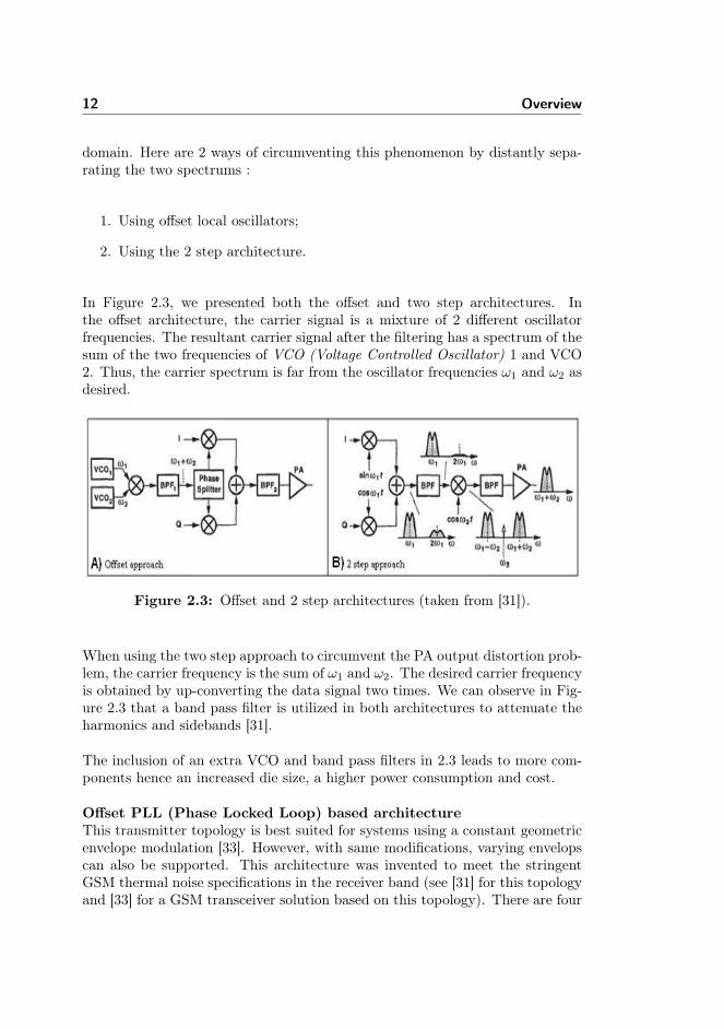
domain. Here are 2 ways of circumventing this phenomenon by distantly sepa-rating the two spectrums :
1. Using offset local oscillators;
2. Using the 2 step architecture.
In Figure 2.3, we presented both the offset and two step architectures. Inthe offset architecture, the carrier signal is a mixture of 2 different oscillatorfrequencies. The resultant carrier signal after the filtering has a spectrum of thesum of the two frequencies of VCO (Voltage Controlled Oscillator) 1 and VCO2. Thus, the carrier spectrum is far from the oscillator frequencies ω1 and ω2 asdesired.
Figure 2.3: Offset and 2 step architectures (taken from [31]).
When using the two step approach to circumvent the PA output distortion prob-lem, the carrier frequency is the sum of ω1 and ω2. The desired carrier frequencyis obtained by up-converting the data signal two times. We can observe in Fig-ure 2.3 that a band pass filter is utilized in both architectures to attenuate theharmonics and sidebands [31].
The inclusion of an extra VCO and band pass filters in 2.3 leads to more com-ponents hence an increased die size, a higher power consumption and cost.
Offset PLL (Phase Locked Loop) based architectureThis transmitter topology is best suited for systems using a constant geometricenvelope modulation [33]. However, with same modifications, varying envelopscan also be supported. This architecture was invented to meet the stringentGSM thermal noise specifications in the receiver band (see [31] for this topologyand [33] for a GSM transceiver solution based on this topology). There are four
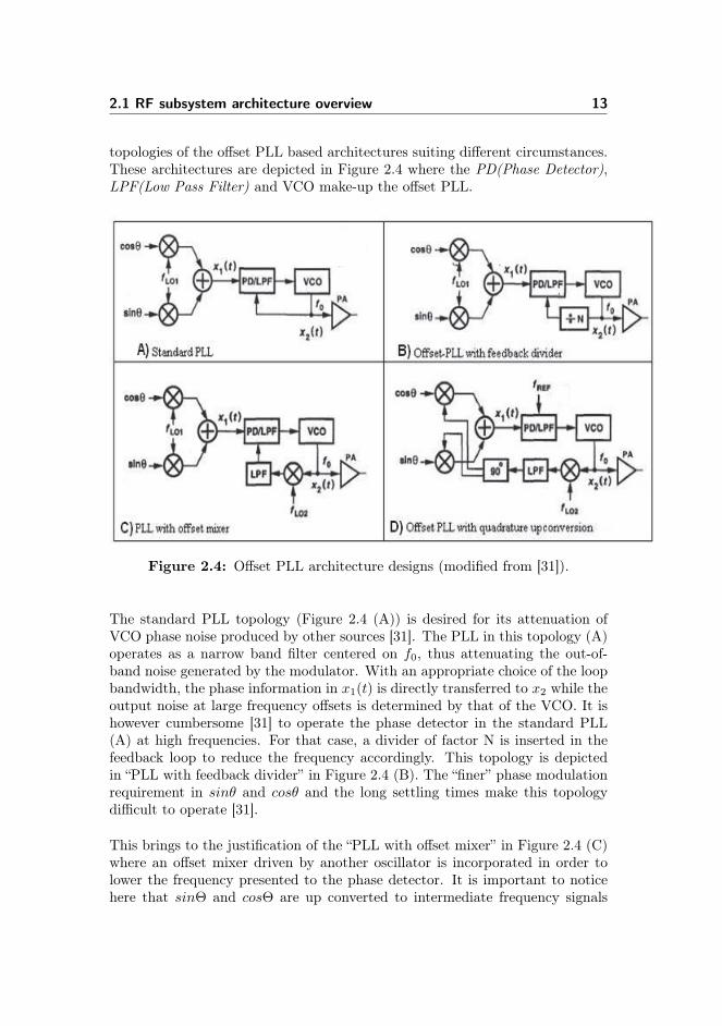
2.1 RF subsystem architecture overview 13
topologies of the offset PLL based architectures suiting different circumstances.These architectures are depicted in Figure 2.4 where the PD(Phase Detector),LPF(Low Pass Filter) and VCO make-up the offset PLL.
Figure 2.4: Offset PLL architecture designs (modified from [31]).
The standard PLL topology (Figure 2.4 (A)) is desired for its attenuation ofVCO phase noise produced by other sources [31]. The PLL in this topology (A)operates as a narrow band filter centered on f0, thus attenuating the out-of-band noise generated by the modulator. With an appropriate choice of the loopbandwidth, the phase information in x1(t) is directly transferred to x2 while theoutput noise at large frequency offsets is determined by that of the VCO. It ishowever cumbersome [31] to operate the phase detector in the standard PLL(A) at high frequencies. For that case, a divider of factor N is inserted in thefeedback loop to reduce the frequency accordingly. This topology is depictedin “PLL with feedback divider” in Figure 2.4 (B). The “finer” phase modulationrequirement in sinθ and cosθ and the long settling times make this topologydifficult to operate [31].
This brings to the justification of the “PLL with offset mixer” in Figure 2.4 (C)where an offset mixer driven by another oscillator is incorporated in order tolower the frequency presented to the phase detector. It is important to noticehere that sinΘ and cosΘ are up converted to intermediate frequency signals

14 Overview
such that fLO2 ± fLO1 = f0. We could also choose to have the quadratureup-converter embedded inside the loop as shown in “offset PLL with quadratureup-conversion” in Figure 2.4 (D). This topology has a constant frequency, fREF ,hence minimizing the phase variation of x1(t) and hence modulating the phaseof x2(t) according to the baseband waveforms.
LINC Transmitters:The LINC (Linear amplifier with Nonlinear Components) transmitter architec-tures employ nonlinear components to form an efficient linear amplifier. Thearchitecture depicted in Figure 2.5 is not commonly used in mobile devices dueto the large number of components required.
Figure 2.5: LINC architecture (modified from [34]).
The transmitter in Figure 2.5 is composed of a DSP (Digital Signal Processor)block and a Tx RF front-end was targeted for mobile WiMAX (Worldwide Inter-operability for Microwave Access) applications [34]. The DSP block contains thesignal component separator (SCS) which decomposes the incoming signal S1(t)into 2 constant amplitude signals whose rectangular representations [I1Q1I2Q2]are calculated and sent to the digital to analog converters (DAC). The analogconverted signals (rectangular representations) are low pass filtered, magnitudeshaped and then mixed with the carrier signal. The mixed signals are amplifiedand then combined into a single RF signal. This architecture enables us to havenonlinear high efficiency PAs at a price of low integration and enlarged chip size.Compared with the direct conversion and polar transmitters, this architectureis impractical and highly costly.

2.1 RF subsystem architecture overview 15
2.1.2.2 Polar Based Transmitters
The polar architectures use the phase and magnitude information to form thecomplex transmitter signal in contrast to the mixer and PLL based architec-tures which employ rectangular modulation. Figure 2.6 depicts the concept of apolar transmitter where the Phase Modulation (PM) is differentiated (dt) intoa frequency fed into the PLL. In Figure 2.7 a fractional-N PLL is used to applythe phase component. The amplitude component is applied by the PA.
Figure 2.6: Polar transmitter (modified from [32]).
Notice the signals after the VCO and PA in Figure 2.6. The magnitude betweenthe signals is meant to underline that it is the PA that does the amplitudemodulation. Figure 2.7 depicts the polar transmitter where the fraction-N PLLis used to apply the phase component.
Figure 2.7: Polar transmitter with fractional-N PLL (modified from [32]).
The fractional-N PLL in 2.7 consists of the following components:
1. A phase/frequency detector (The phase modulator (PM) is differentiated

16 Overview
into the frequency used by the Frequency Modulator(FM));
2. Loop filter;
3. VCO;
4. Feedback counter;
5. Delta-Sigma Modulator ( ∆ΣM) [35].
The PLL is used by the polar transmitter to apply phase modulation to the RFcarrier.
There are two inputs to the polar transmitter, the phase modulation and theamplitude modulation. The amplitude modulation is fed directly to the PAthat amplifies the carrier signal accordingly. This is very desirable for powerconsumption as it gives an opportunity of scaling the PA other than having aconstant gain. On the other hand, the phase modulation is differentiated andconverted to analog before being fed to the VCO. The possibility of varying thepower levels of the PA suits LTE as this technology has varying geometric en-velops. This architecture is however undesired due to its practical imperfectionsleading to spectral re-growth, increased error vector magnitude (EVM) and linkperformance loss [32]. These imperfections are scrutinized and illustrated in[20].
2.1.2.3 Evaluation of the architectures
The evaluation of the transmitter architectures is conducted in this section ac-cording to our perception. The architectural designs of the direct conversion,polar and LINC transmitters have been elaborated in the previous sections. Intable A.3 where the power efficiency comparison between the 3 architecturestargeted for WiMAX is presented, we can see that the direct conversion archi-tecture has the least number of components required and the worst PA andsystem efficiency. The polar and LINC transmitters respectively require 50%and 100% more components than the direct upconversion transmitter. Thepolar transmitter has the best performance in terms of power efficiency. Thisefficiency can only be achieved if the strict matching, high sampling rate DACand a good polar PA can be guaranteed.
In Table A.4 we present the overall architectural evaluation of the transmitterarchitectures based on the transmitter size, power consumption, system effi-ciency, PA efficiency and the complexity level. The polar transmitter (withoffset loop including the PA) have the best performance but also the highest

2.1 RF subsystem architecture overview 17
complexity which makes it practically undisired. Practically, the most desirabledesign is the direct conversion architecture, as also preferred by most vendorsand authors, due to its simplicity and a high level of integration. We have alsoseen the direct conversion architecture pulling problems and ways of mitigatingthem. The most efficient way of migrating this problem without increasing thecomponent number dramatically is the generation of the LO signal with the fre-quency as twice as the channel frequency. This would merely require a divider infront of the mixers. Moreover, [36] states that the direct conversion transmitteris the de facto standard for both LTE and WCDMA (Wideband Code DivisionMultiple Access.
2.1.3 Current trends for LTE transmitters
Due to the fact that LTE is a relatively new technology, there have neitherbeen produced nor published numerous transceivers as in comparison with itspredecessor technologies as the WCDMA and WiMAX. The available WCDMAtransceivers are mainly designed upon the homodyne and heterodyne architec-tures. A correlation between the chosen architecture and the used technologycan be observed. The Complementary Metal Oxide Semiconductor (CMOS)technology [37], [38], [39] is used with the homodyne architectures as the SiliconGermanium Bipolar CMOS (SiGe BiCMOS) technology [40], [41], [42] is usedwith the heterodyne architecture. An intriguing factor of notice between thesolutions of these two technologies is the die sizes. The CMOS solutions are30% larger than their counterparts.
Performances of homodyne and heterodyne transmitters produced in both CMOSand SiGe BiCMOS for WCDMA are presented in tables A.1 and A.2 in the ap-pendix. It can be observed that transmitters in both tables A.1 and A.2 domeet the WCDMA specifications. The parameters, cost and reproducibility areneeded in order to make a conclusive distinction.
The technological and architectural trends of the CMOS and homodyne inWCMDA and WiMAX have been followed up to the LTE by the first vendorsof the LTE transcievers. Infineon [43] and Altair Semiconductor [44] providedthe first highly integrated LTE solutions of 5 × 5mm2 and 4.4 × 2.9mm2 re-spectively. Both these transmitters are produced in 130nm CMOS technologyusing the homodyne architecture. These are good solutions in terms of poweras they are a technology node lower than the existing solutions for WCDMA(see appendix). The relationship between the technology nodes and the currentconsumption where the positive correlation between the technology nodes andthe current consumption was demonstrated in [45].

18 Overview
2.1.4 Future trends
The review of the research in the RF transceivers reveals the desire of striving toextend the digital part of the RF transmitters as close as possible to the analogpart of the RF transmitters and the antenna. This is much desired due to thesignificant development in digital signal processing (DSP) where IQ mismatches,phase noise and other RF imperfections [46] can be nearly perfectly compen-sated using DSP algorithms. This trend fits best with the CMOS technology asit is most compatible with digital signals. As mentioned earlier, as the homo-dyne architectures are developed in CMOS technology, this combination wouldyield highly integrated and low cost solutions. There are digital transmitterssolutions in CMOS targeted for GSM and EDGE [47] [48]. These solutions wereused in cellular phones though they had a reproducibility issue. If the lessonslearnt from the mentioned solutions are taken up, we would definitely expectthe digital trend to continue more into practice (as seen in [43] and [49]) to-wards the new technologies as the LTE. We have an emerging technology, ininfant stages, called Software defined radio (SDR) [50], [51] which is intendedto implement a broader range of capabilities through elements that are softwareconfigurable in the micro-level communication objects (MCO). For the meantime, the conventional hardware defined radios are many factors cheaper andpractical compared to the complicated SDRs. The US military is the drivingforce behind this technology. A Software Communication Architecture (SCA)that enables the integration of hardware and software components from differentvendors into seamless products has been designed. For daily users, we could beable to have cellular phones that could operate with all commercial providersacross the world. As the cellular phones emerged from the military, it can behard to rule out that the SDRs might not be in public use within a decade orless.
2.1.5 Summary
We have seen the state of art of the RF transmitters, their corresponding tech-nologies and evolution towards the LTE technology. The available LTE trans-mitter solutions [43], [49] and [44] are produced in 130nm CMOS technologyusing the direct conversion architecture though [49] also offers a polar solution.The CMOS technology is currently undesired because it needs lots of calibra-tions due to its high tolerance values. But it is understandable that the existingsolutions choose this technology due to the low production cost.
Based on the review of the available RF transmitter solutions and publications,the most efficient, low cost and high integration transmitter solution for the LTE

2.2 LTE Review 19
would be the direct conversion architecture with a digital front end producedpreferably in CMOS technology. In order to have a conclusive decision, ananalytical analysis towards LTE, as in table A.3 for WiMAX, would be neededto support this observation.
The choice of the transmitter architecture and technology solution is also contin-gent on the performance of the corresponding receiver solutions as in practicalterms, the transmitter and receiver do share the same RFIC.
In the next section, we are reviewing the LTE telecommunication technologywhich is the target technology of this work.
2.2 LTE Review
2.2.1 Introduction
The LTE(Long Term Evolution) technology is the next generation of cellularphone technology and is intended to reach high peak data rates of 100Mbpsdown link and 50 Mbps uplink (Release 8), low latency, high radio efficiency,low cost and high mobility characteristics.
The cellular phone technology has grown rapidly as the demand for more ad-vanced and sophisticated features increases. The cellular phones that were oncesolely used for vocal and text communication via short message services (SMS)have evolved into multimedia gadgets demanding data rates of broadband ca-pacity for optimal operation. The LTE technology is a way forward towardscellular broadband data rates [52]. This review is based on LTE release 8 [52]and we will also peep at the features to expect in releases 9 and 10.
2.2.1.1 The LTE targets
The LTE technology is supposed to meet the following specifications:
• High performance;
– A peak data rate of 100 Mbps and 50 Mbps in downlink and uplinkrespectively for User Equipment (UE) category 3. For UE category5, 300 Mbps and 75Mbps for downlink and uplink respectively areexpected;

20 Overview
– 1Gps in downlink and 500Mbps in uplink for advanced LTE;
– Faster cell edge performance;
– Reduced RAN(Radio Access Network) latency for better user expe-rience;
– Improved spectrum efficiency ( 2 to 4 times compared to HSPA Re-lease 6);
– Scalable bandwidth of [20 15 10 5 3 1.4] MHz;
– Improved broadcasting;
– IP optimized (focuses on services in the packet switched domain).
• Backward compatibility;
– Compatibility with the existing GSM/EDGE/UMTS systems;
– Ability to utilize the existing 2G and 3G spectrum;
– Support hand-over and roaming to the existing mobile networks.
• Wide application;
– TDD (unpaired) and FDD (paired) spectrum modes;
– Mobility up to 350kph;
– Large range of terminals (phones and PCs to cameras).
2.2.2 The LTE structure
The relevant part of the LTE structure, LTE E-UTRAN architecture [53], forthis work is presented in Figure 2.8. The extensive structure of the whole LTEsystem can be seen in Figure A.3 in the appendix.
• User Equipment (UE)The UE is the device used by the end user for communication. This is inmost cases a hand held device in form of a cellular phone or a laptop. Thisdevice is equipped with a Universal Subscriber Identity Model (USIM) forits identification and authorization. LTE UEs in form of USB (UniversalSerial Bus) dongles are now deployed around the world. We are interestedin the performance of this device in terms of power consumption and theemitted electromagnetic energy produced during the transmission of theLTE signal to the eNB;

2.2 LTE Review 21
Figure 2.8: The LTE E-UTRAN structure made up of the UE and base station(eNB or eNodeB). This structure maintains the UE on the networkvia the radio link (LTE-Uu) (taken from [53]).
• Evolved Base Station(eNB)The eNB is the radio base-station that is in control of all radio relatedfunctions in the fixed part of the system. The functions of the eNB arelisted below:
– The eNB acts as a layer 2 bridge between the UE and the Evolved-Packet Core (EPC) by being the terminal point of all the radio proto-cols towards the UE and relaying data between the radio connectionand the corresponding IP based connectivity towards EPC. In thisrole as the terminal point, the eNB performs ciphering/decipheringof the uplink data and also IP header compression/decompression;
– The eNB also performs the following control plane functions;∗ Radio Resource Management which involves controlling the us-
age of the radio interface;· Allocating resources based on requests;· Prioritizing and scheduling traffic according to required Qual-
ity of Service;· Constant monitoring of the resource usage situation;
∗ Mobility Management;· handovers;
The eNB, as a static element with the UEs in its vicinity as the dynamicelements, is very influential on the amount of power and electromagneticradiation used for transmission from the UEs. The UE power consump-tion/electromagnetic energy used to reach the eNB is (among other fac-

22 Overview
tors) a function of the distance and terrain from the UE to eNB. TheeNB dictates the transmission power of the UE by sending ramp up/downmessages whenever necessary.
For the relevance of transmitter power consumption and the emitted elec-tromagnetic radiation, it is the air interface (in the uplink direction) inthe E-utran structure that is of interest. In this technology, for any trans-mission to occur, there must be allocated resources in form of resourceblocks as we will see in the LTE technology section. Resource blocks aretwo dimensional time-frequency elements of 7 OFDMsymbols(0.5ms) ×12 subcarriers. The LTE air interface defines a 10ms radio frame com-prising of ten 1ms subframes of two 0.5ms slots. There can be 6 or 7(control or data) symbols in a single slot depending on the used cyclicprefix(see OFDM transmission section). Hence, for power consumptionand radiation measurements, the analysis of the contiguous 2 × 0.5msslots (subframes) would form a basis for the calculation of the power con-sumption and radiation emissions of the UE scenarios.
2.2.3 Emulation realization of the LTE structure
In this work, we wish to emulate the power consumption and the emitted elec-tromagnetic energy during the transmission of the LTE signal. The goal is tobe able to emulate these values very early in the design phase, when the firstprototypes with physical layer functionality are available. At this stage, the pro-totypes are neither capable nor allowed to connect to an E-UTRAN network.Moreover, even if we are capable of connecting to the E-UTRAN network, mea-surements conducted would not be repeatable to due to the unpredictability ofthe air interface. Hence, we would have to emulate the E-UTRAN architecturein the laboratory environment. This would take a one-two cell protocol testerwith LTE compatibility. The prototype would be connected to the protocoltester via the antenna port using a coaxial cable. When connected, the proto-type is invoked to search for a cell until its connected to the protocol tester. Wehave in this work used the AT4 wireless and Anritsu MD8430A protocol testers.
2.2.4 The LTE technologies
The LTE evolution was motivated by the high data rate demand where a combi-nation of radio resource effective methodologies of modulating and transportingdata were applied.
The LTE technology is made up of 3 fundamental technologies:

2.2 LTE Review 23
1. The Orthogonal Frequency Division Multiple Access (OFDMA) used fordownlink;
2. The Single Carrier- Frequency Division Multiple Access (SC-FDMA) usedfor uplink;
3. The Multiple input Multiple output (MIMO) used for both downlink anduplink.
2.2.4.1 The OFDMA
This section describes the OFDMA principles used in the LTE technology inthe downlink direction.
Introduction: OFDMA is a technology that has evolved from Frequency Di-vision Multiplexing (FDM) and Orthogonal Frequency Division Multiplexing(OFDM) with the inclusion of Time Division Multiplex Access (TDMA)principles.The FDM technology was the first multicarrier technology and it is widely usedin the television transmitters. The main drawback of this technology was itsspectral inefficiency due to the requirement of guard bands between the carriersas seen in Figure 2.9. Consequently, the OFDM technology was proposed which
Figure 2.9: The FDM modulation requires guard bands between channelswhich makes it very spectrum inefficient.
was also based on the multi-carrier principles but eradicated the necessity of theguard bands by utilizing the orthogonal sub channels as shown in Figure 2.10.
Given the same resources as in Figure 2.9, we can observe the amount of spec-trum that can be saved by using orthogonal sub-channels in Figure 2.10. Theorthogonality is achieved by choosing the spacing between the sub-carriers suchthat at the sampling point of the individual sub-carriers, the other sub-carriershave 0 values. This feature is illustrated by Figure A.1 in the appendix. InFigure A.1, the spacing of 15KHz makes it possible to have all the other sig-nals at 0 value at the sampling point of the desired one. The orthogonality of

24 Overview
Figure 2.10: The OFDM modulation applying orthogonality to differentiatebetween channels. The orthogonality eliminates the use of guardbands yielding spectrum efficiency.
OFDM depends on the condition that the transmitter and receiver do operatewith exactly the same frequency reference. The utilization of cheap componentsin UEs do make this problem severe as these oscillators do have large tolerances.The automatic frequency control in the UEs helps make sure that the frequencyoffsets never get out the bound set by the specification. Thus, the orthogonalityin OFDM is still intact also given these impairments.
The OFDM technology solely allows a single user on a channel at any giventime. For a system using OFDM modulation to accommodate multiple users onthe same channel, TDMA has to be applied so that each user can have a shareof the channel for a given TDMA slot. This is illustrated in Figure 2.11
Figure 2.11: OFDM employing TDMA to enable the sharing of channels be-tween different users. Each user, represented by a colour, is allo-cated a slot on the channel.
The colors in Figure 2.11 represent the different users. Thus, each user occupiesthe channel for a given amount of time. This is very inefficient considering thepossibility that the user might not need the full capacity of the channel in the

2.2 LTE Review 25
allocated time. In order to fully utilize the capacity of the channel, the diver-sification of the channel in time and frequency domain is applied. This resultsinto the division of the channel; see Figure 2.13, where each column(channel)is divided among different users for a specified duration, hence increasing thecapacity of the channel. This diversification of the OFDM channels into afrequency-time grid, is what is referred to as the OFDMA technology.
Thus, the 2 LTE technologies OFDM and OFDMA differ in principle thatOFDM is a modulation scheme and OFDMA is the access scheme used to effec-tively diversify the resources (OFDM channels) among different users accordingto their bandwidth necessities.
In the LTE technology, in the downlink direction, the users are assigned re-sources in form of resource blocks comprising of 12 subcarriers over a durationof a half millisecond. Practically, the allocation resolution of 1ms is used in timedomain.
OFDM transmission: Figure 2.12 depicts the OFDM transmitter where aserial bit stream of data in frequency domain is parallel transformed into thevector S whose dimension spans the available number of subcarriers. Eachelement of the vector S is individually modulated into the complex vector Xthat is IFFT’ed to produce the time domain samples. Here, it is important tonotice that N ≥ M as the IFFT demands a power of 2 inputs. Zero padding isused for N −M samples. Due to the problems that might arise because of theInter Symbol Interference (ISI) when the length of the channel is longer thananticipated, assurances must be provided to mitigate this. This assurance inthe LTE technology is provided inform of cyclic prefices as shown between theIFFT and P/S in Figure 2.12.
The cyclic prefix principle implies the copying of a chunk (of specified length)of the ending of the symbol to the beginning of the symbol as illustrated inFigure 2.12 with the samples [Xk[N −G]...Xk[N −1]] being appended the inputof the P/S. The cyclic prefix has 2 possible lengths depending on the type usedaccording to the 3GPP specification [52]. There is short and extended cyclicprefices of durations 4.7µs and 16.7µs respectively that can be applied. Thetype of cyclic prefix applied do affect the number of symbols in the 0.5ms slot.Here with the short cyclic prefix, we do have 7 symbols and 6 symbols with theextended cyclic prefix. Thus, we do have a data payload reduction when theextended cyclic prefix is used and it is therefore infrequently used. The tradeoff between using a short cyclic prefix with seven symbols is greater than thepossible degradation from inter-symbol interference due to channel delay spreadlonger than the cyclic prefix. Thus, the extended cyclic prefix is seldom used.This does also gain power consumption and radiation minimization as we areable to send more information data with the short prefixes. The output of the

26 Overview
Bit
stream
in freq.
domain S/P IFFT
P/S
. . . .
. . . .
. . . .
. . . .
. .
.
S [1]
S [0]
S [M-2]
S [M-1]
X [M-2]
X [M-1]
X [0]
X [1]
.
.
.
.
.
.
.
.
.
k
k
k
k
k
k
k
K
X [0] k
X [1] k
X [N-G] k
X [N-1] k
Cyclic prefix
To the transmission
Circuit
Modulation
Figure 2.12: OFDM transmitter.
P/S in Figure 2.12 is analog converted for transmission. In the LTE technology,it is the eNB that does the operations depicted in 2.12 and transmits the outputanalog signal to the appropriate user equipment. For the transmission from theeNB to take place, resources have to be allocated inform of resource blocks asmentioned earlier. Thus, providing a group of subcarriers to a specific UE for agiven period of time as depicted in Figure 2.13.
Figure 2.13: OFDMA allocation providing the possibility of allocations inboth time and frequency domains.

2.2 LTE Review 27
2.2.4.2 SC-FDMA
In the uplink direction of the LTE system, the SC-FDMA technology is usedin contrast to the OFDMA technology used in the downlink direction. TheOFDMA would have been very practical to have in both directions. However,due to OFDMA’s high requirement of Peak-to-Average Power Ratio (PAPR)and the demand for power efficient handheld devices, OFDMA is to be usedin the base station where we do not have limited resources in terms of power.The SC-FDMA utilizes the desirable characteristics of the OFDM and the lowPAPR of single-carrier transmission schemes to make an efficient LTE uplink.The OFDM characteristic of main interest here is the division of the transmis-sion bandwidth into orthogonal parallel subcarriers where the orthogonality isachieved by:
• Employment of the cyclic prefixes that are longer than the channel delayspread;
• Synchronization of the received signal in time and frequency;
• Users occupying different sets of sub-carriers.
The SC-FDMA signals can be made in both time and frequency domains wherethe resultant SC-FDMA signals are equivalent. There is though a difference inthe bandwidth efficiency where the time domain procedure is less bandwidthefficient due to the time domain filtering and filter ramp up/down time require-ments. Let us start with the time domain implementation of the SC-FDMAshown in Figure 2.14.
The incoming bit stream is serial to parallel converted and then modulatedby either QAM or QPSK modulation schemes. The modulated bits can bedirect-sequence spread to spread the signal energy over a wider band but thisis optional. The repetition block following the spreading is also optional. TheQPSK or QAM modulated bits after the optional processing is translated tothe desired frequency within the available bandwidth. This data is finally cyclicprefixed, pulse shaped and transmitted. The frequency domain generation ofthe SC-FDMA signal distributes the modulated signals to sub-carriers usingthe Discrete Fourier Transform (DFT). This transmission scheme is depicted inFigure 2.15.
The frequency domain transmission scheme maps the QPSK/QAM modulatedsymbols into the subcarriers m by the DFT operation. The m subcarriers mustbe a factor of 2n × 2k × 5l according to the specification. This was meant forthe feasibility of the DFT. The subcarriers are then mapped to an N-IFFT

28 Overview
In coming
Bit stream Serial to
parallel
converter
User specific
block
repition
De-
spreading
Bits to
constellation
mapping
M bits
X
User-
specific
Frequency
shift
Add cyclic
prefix
Pulse-shape
filter
Transmission
circuity
V
Optional
Figure 2.14: TDD (Time-Division Duplex) generation of of the SC-FDMAuplink signal.
and notice here that given the restrictions on both m and N, they are neverequivalent. Thus, also in this case as in the OFDM, the non-used sub-carriersare zero padded.
2.2.4.3 Multiple Input Multiple Output
Multiple Input Multiple Output (MIMO) uses spatial multiplexing [55], beamforming [56] and pre-coding [57] principles where different TX’s are sent fromdifferent antennas with different data streams in the transmitter at the sametime. On the receiver side, the data streams are detected by signal processingmeans utilizing the propagation channel characteristics. To illustrate how thetransmitted signals are detected in the receiver, let us assume that we have a4× 4 system depicted in Figure 2.16:

2.2 LTE Review 29
Figure 2.15: FDD generation of the SC-FDMA uplink signal (Taken from[54]).
Transmitters Channels Signal at the receiverTx1 h00...h03 Rx1 = Tx1 × h00 + Tx2 × h10 + Tx3 × h20 + Tx4×
h30 +W1
Tx2 h10...h13 Rx2 = Tx1 × h01 + Tx2 × h11 + Tx3 × h21 + Tx4×h31 +W2
Tx3 h20...h23 Rx3 = Tx1 × h02 + Tx2 × h12 + Tx3 × h22 + Tx4×h32 +W3
Tx4 h30...h33 Rx1 = Tx1 × h03 + Tx2 × h13 + Tx3 × h23 + Tx4×h33 +W4
At the mobile terminal in Figure 2.16, we can see that we have 4 equations with4 unknowns which can be mathematically solved. The noise (W1...W4) makesthe detection process very difficult. However, by using the reference signals,the channel propagation can be estimated and the transmitted signals can beseparated.
The application of this technology should in principle enhance the peak datarate by a factor 2 using a 2 by 2 antenna configuration or a factor 4 using a4 by 4 antenna configuration. However, when you move to higher data ratesby packing more data in the same amount of time, the bit error rate usuallyincreases. This leads to a demand of higher coding rates. Thus, for the sameamount of signal-noise-ratio, the information data rate increases slightly lessthan factor 2 or 4 for 2 by 2 and 4 by 4 respectively. The MIMO technology is

30 Overview
Figure 2.16: MIMO (taken from [54]).
illustrated in 2.16 where the transmit diversity principle can be observed as thesame signal is sent from different transmitters in the base station and receivedon all receivers in the mobile terminal in order to exploit the gains from theindependent fadings’ between the antennas. The system in 2.16 is meant forillustration purpose as the number of antennas (per now in LTE release 8) inthe UEs is set to 2 [58]. We can however have 2, 4 and 8 antennas at theeNB and [58] shows that the antenna array of 2× 8 is the best inform of sectorand edge throughput. This comes at a 50% increase in cost and complexitycompared to the 2× 2 configuration.
2.2.5 LTE future trends
LTE-A (release 10) is currently under definition. This release is supposed toprovide downlink and uplink data peak rates of around 1 Gbps and 0.5 Gbpsrespectively with a spectrum efficiency of 30bps/Hz and 15bps/Hz in downlinkand uplink. LTE-A will provide a 83% increase in spectrum efficiency comparedto the LTE technology available on the market (release 8). The LTE-A is in-tended to utilize the carrier aggregation methodology to increase the availablebandwidth to 100MHz. Moreover, the MIMO diversity is to be further exploitedwhere there are plans to use the 4×4 and 8×8 MIMO configurations. With theanticipated backward compatibility between LTE/LTE-A, we can thus expecta LTE/LTE-A technology that meets the IMT (International Mobile Telecom-munication) advanced 4G requirements before the end of this decade.

2.2 LTE Review 31
2.2.6 LTE structural and technological influence on radi-ation and power consumption
Having seen the structure and the technologies behind LTE in the previoussections, let us take a look at how the structure and technologies of the LTEwould influence the emitted radiation and dispensed power. It is well knownthat the LTE technology was developed to meet the high data rate demand ofthe wireless handsets. LTE is targeted to provide 100Mbit/s and 50Mbit/s fordownlink and uplink respectively for category 3 and slightly higher for category5 as mentioned earlier. It is the radiation and power consumption during uplinktransmission that is of interest here. Thus, watts consumed and w/Kg absorbedin a body per throughput bit.
In frequency domain, the OFDMA transmission consists of several parallel sub-carriers where the time domain equivalent is a sum of these subcarriers (sinu-soids). The geometrical envelop of the time domain waveform representationtends to vary strongly leading to a very high PAPR. The PAPR of this magni-tude leads to a large back-off requirement in the design of the PAs and this is thereason that OFDMA is only to be used in basestations in the LTE technology.On the other hand, the usage of SC-FDMA in the uplink is a very good choicein terms of PAPR and PA efficiency as the resultant waveform of SC-FDMAbehaves as a single sinusoid with low PAPR. Hence, a very good PA efficiencyfor the uplink which is very desired as UEs run on batteries. See Figure A.2in the appendix which depicts the relationship between the geometric envelopand the PA back-off requirement. Crest factor reduction (CRF) schemes havebeen proposed as in [59] to reduce the OFDM PAPR though they have not beenapplied in the LTE yet.
The LTE technology “MIMO” and the signal processing techniques “beam form-ing” and “pre-processing” are very beneficial for power consumption and emittedradiation. With the MIMO technology, we do have a data rate increase of somefactors depending on the MIMO configuration. Therefore, the necessary cod-ing is also reduced as the different received signals are used to estimate thetransmitted signal. Hence, the more data we are capable of transmitting in thesame amount of time and power, the more power and radiation we are saving.However, the increased number of transmitters make the user more exposed tothe electromagnetic energy. A beam forming technique which ensures direc-tional transmission is also employed in LTE. With the directional transmission,the necessary transmission power can be reduced also yielding a reduced powerconsumption and emitted radiation.
In the telecommunication forecasts [60], it is fore-casted that a subscriber in aEuropean country would have a daily traffic of 495Mb between 2010 and 2020.

32 Overview
This value does though not differentiate between uplink and downlink data. Aswe are interested in the uplink data and for that case the performance of UEs,it would be of best interest to get statistics of the ratio between the uplink anddownlink in order to estimate the fraction of 495Mbits that is uplink. Thesestatistics are rather very confidential for service providers and not easy to get.The daily uplink data usage for an average person would give an insight in theamount of power that can be saved by optimizing and reducing the necessarypower per uplink bit. The proposed LTE advanced release 10 which among othermethodologies is to utilize carrier aggregation to provide data rates of 1Gps indownlink and 500Mbps in uplink would sufficiently handle the projected dailyuser traffic of 495Mb with an anticipated lower power and emitted radiation perbit.
2.2.7 Summary
This preview has discussed the LTE structure, the applied technologies andthe LTE’s structural and technological influence on radiation and power con-sumption. We have seen the PAPR issue that rendered the LTE from having atechnological (OFDMA) symmetry between uplink and downlink. Based on theprojected data usage and the targeted data rates for LTE and LTE advancedtechnology, we can be certain that the technology will satisfy the data hungryusers. An intriguing factor of curiosity is the efficiency of the LTE technologyin terms of power (watts) and absorbed SAR per bit.
In the next section, the available power estimation methodologies are presented.
2.3 Power consumption estimation overview
Extensive work has been published on the estimation of power consumption atvarious levels of abstraction [7–10]. Figure 2.18 shows the levels of abstractionduring the design of SoC (System-on-Chip) systems. We can observe that theamount of information increases by order of magnitude as the design maneuversfrom system level to transistor level [11]. Consequently, the accuracy of powerconsumption estimation also increases as more knowledge is gained when thedesign transverses from the system level to the transistor level.
Approaches for power estimation at different levels of abstraction have beencommercialized into power estimating tools [12–17]. The applicability of thePowerTheater [15], SpyGlass [13] and Cadance power estimation/emulation [12]

2.3 Power consumption estimation overview 33
1E0
1E1
1E2
1E3
1E4
1E5
1E6
1E7
Number of componentsLevel
Gate
RTL
Algorithm
System
Transistor
Ab
str
ac
tio
n
Ac
cu
rac
y
Figure 2.17: SOC design levels of abstraction (taken from [61]) showing thatthe abstraction decreases, as more knowledge is gained about theSOC. Thus, the power estimation approach after the transistorlevel presented in this work should be more accurate than thestatus quo approaches at the system, RTL and gate levels ofabstraction.
tools was analyzed in a feasibility study conducted by Nokia [18]. These ap-proaches are appropriate for digital circuits with discrete signals as they takethe discrete transitions and technology libraries as inputs to estimate the powerconsumption of a given digital device.
Power estimation methodologies of analog circuits which are of interest in thiswork, have been defined at the system level of abstraction [19–22, 62]. Thesemethodologies are based on the notion that the estimated power value is thepower consumed by a functional block when given relevant input specifications,such as the target technology, without knowing the detailed implementationof the block. It is very difficult to achieve accurate power estimations at thislevel of design because all architectural decisions and relevant details as circuitimplementations are not defined yet [20]. Power estimation of analog circuits isusually based on spreadsheets and experiences/expertise of system architects.In this way, relatively good power estimations can be produced because in mostcases the new designs are based on old designs with minimal modifications.
Power estimation (status quo) of analog circuits at system level takes either ananalytical or empirical methodology where a top-down or bottom-up approachis applied. However, the analog power estimators are always a blend of the twoapproaches with emphasis on one. In analytical methods, power consumption ismodeled as a mathematical function derived from known schematics of the topol-

34 Overview
ogy of a component while in empirical methods measured power consumption isassociated with each state/transtion of a component. The bottom-up and top-down approaches for developing power estimators for analog circuits [19,20,22]:
• The bottom-up approach, in analytical terms, requires a certain topologyto be chosen from which exactly known schematic equations are derived,thereby modeling the behavioral model of the analog block. The require-ment of the topology is a disadvantage for this approach as it is not the casein architectural system exploration. However, this increases the accuracyof the approach. In empirical terms [20], the power consumption of eachcomponent is measured or extracted from transistor level simulation forthe different states. Here, parameters that influence the power consump-tion of the component for all operation states and transitions between twostates are varied within their operational range and the power consump-tion per state computed/measured. This results into power consumptionlookup tables for each operational state of each component. However, it israther ambiguous on how measurements and transistor level simulationscan be conducted at the system level of abstraction;
• The top-down approach suites the system level approaches better as notopology assumptions are required. Herein, the power behaviors of thecomplete system are modeled. However, this comes at a cost of the accu-racy as the accuracy of models is difficult to achieve because of the typicalnature of analog designs where one transistor can have a great impacton the behavior and specification of the design. Meanwhile, the use offitting parameters typically compensates this constraint towards differenttopological implementations of the same analog block.
2.3.1 Analytical power consumption estimating method-ology
The available analytical power estimators for analog power consumption takeinput specifications as target technologies to compute the power estimate of afunctional block [19]. These estimators are constrained by two requirements [63]:
• Should only take high level block parameters as inputs in order to speedup the exploration of new designs;
• The accuracy of the estimation should be within a first order range.
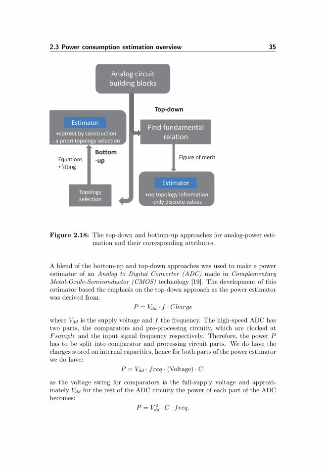
2.3 Power consumption estimation overview 35
Analog circuit
building blocks
Find fundamental
relation
Top-down
Figure of merit
+no topology information
-only discrete values
Estimator
Topology
selection
Equations
+fitting
Bottom
-up
+correct by construction
- a priori topology selection
Estimator
Figure 2.18: The top-down and bottom-up approaches for analog-power esti-mation and their corresponding attributes.
A blend of the bottom-up and top-down approaches was used to make a powerestimator of an Analog to Digital Converter (ADC) made in ComplementaryMetal-Oxide-Semiconductor (CMOS) technology [19]. The development of thisestimator based the emphasis on the top-down approach as the power estimatorwas derived from:
P = Vdd · f · Charge
where Vdd is the supply voltage and f the frequency. The high-speed ADC hastwo parts, the comparators and pre-processing circuity, which are clocked atFsample and the input signal frequency respectively. Therefore, the power Phas to be split into comparator and processing circuit parts. We do have thecharges stored on internal capacities, hence for both parts of the power estimatorwe do have:
P = Vdd · freq · (Voltage) · C.
as the voltage swing for comparators is the full-supply voltage and approxi-mately Vdd for the rest of the ADC circuity the power of each part of the ADCbecomes:
P = V 2dd · C · freq.

36 Overview
To this point, the power estimator of the ADC has been based on the top-downapproach. However, the capacitances are topology and technology dependentwhich is part of the bottom-up approach hence a blend of the two approachesto achieve the total power estimator:
P ∝ V 2dd · Lmin · (Fsample + Fsignal)
where the equality is replaced by the proportionality as the capacitance is takenproportional to the technology’s minimal channel length Lmin. The accuracyof the power estimator must also be included in the computation of the powerestimator as the accuracy can be varied through the size of the device [64]where larger devices do produce higher accuracies at a cost of increased totalcapacitance leading to limited speed and increased power consumption. Theaccuracy ENOB (effective number of bits) is a function of SNDR (signal-to-noise-and-distortion ratio) defined as [65]:
ENOB =20 · log(SNDR)− 1.76
6.02
The investigation based on a 75 data points for the correlation between accuracy,device size and power resulted in a regression relation [19]:
log
(V 2dd · Lmin · (Fsample + Fsignal)
Power
)= −0.1525 · ENOB + 4.8381
And thus, the final-power estimator valid for the complete class of CMOSNyquist-rate high speed ADCs is [19]:
P =
(V 2dd · Lmin · (Fsample + Fsignal)
10−0.1525·ENOB+4.8381
).
Power estimator models for each of the components in the analog signal chain ofa transceiver were presented in [62] also using an analytical approach blendingthe top-down and bottom-up approaches. The practicality of the analyticalapproaches [19,62] can be questioned as they lack the validation against realisticscenarios. For an RF subsystem of interest in this work, it would be impracticalto define an analytical model for each and every component. Thus, in this workwe are proposing a methodology that considers the RF subsystem as a singlecomponent but to our knowledge, there is no analytical model that defines thepower consumption of a RF subsystem.
2.3.2 Empirical power consumption estimating methodol-ogy
Empirical methods for modeling the power consumption of the analog circuitswith the intent of power estimation and optimization are presented in [20,22]. In

2.3 Power consumption estimation overview 37
the power estimation approach in [20], a state-based power estimation method-ology at system level for integrated RF Front-ends is presented. Here, powerstate machines which are usually applied in power models of digital microelec-tronics were modified for analog components. The approach also follows theblend in the middle paradigm to compute the power models. In this approach,components are described by a power model made up of the power (PSM) andfunctional (FUSM) state machines, shown in Figure 2.19, which interact witheach other.
FUSM
PSM
In
Out
In
Out
Power control signals to/
From components
with lower Power hierarchy
Power control signals to/
from components with
higher power hierarchy
Figure 2.19: The system level power model of a component of an RF front-end is made up of PSM and FSUM state machines. The PSMmodels the power behavior of the component and the FSUMmodels power related control behaviors.
The PSM module is implemented by the power profiles, of the component ofinterest, obtained from the bottom-up approach. This module computes theestimated power of a component as a function of the power control signals, asOFF, Ready and ON, to/from components with higher power hierarchy andthe power states from the FSUM module. The RF device is a passive devicethat operates on the control mechanisms or commands from the RF control orDigRF interface, hence, these mechanisms and commands are relevant for powerconsumption. The FSUM models these control mechanisms/commands whichare regarded as the power states of the components with lower hierarchy. A casestudy of this approach was performed for a zero-IF receiver where it is statedthat the operational states of a receiver are entirely determined by the baseband.Herein, the power commands from the baseband are sent to the PSM of the RFfront-end’s DigRF interface. The PSM of the DigRF interface controls the statesof its corresponding FUSM. The FUSM of the DigRF interface is responsiblefor interchanging power commands with the PSM of the RF control hence the

38 Overview
RF control has a lower power hierarchy. This approach assigns a power valueto each state of a component in a look-up table which would work perfectlyfine given a limited number of states a component can find its self in and thisapproach could be applied at any level of abstraction of a design. However, theimpracticality of this approach arises due to the size of the lookup table thatwill be required for technologies like the LTE. Here, you find parameters as Txpower, signal bandwidth and carrier frequency on the DigRF interface betweenthe baseband and the RF device (subsystem) which would require thousandsof elements in a look-up table. Thus, in this work, we do abstract away thestate machines but do the characterization of a component as illustrated inthe bottom-up approach. In order to avoid the complexity of mapping thepower with the various states, we do a mathematical mapping that maps thelow level parameters to the power consumption of the device. Thus, whengiven a combination of low level parameters, the estimated power would be amathematical mapping between the model and the low level parameters.
Another empirical method based on neural networks for analog power modelingwas presented in [22]. In this approach, power measurements are conductedfor a specific analog component at various states and the power consumption ismodeled with a continuous function obtained via a neural network. This con-tinuous function is integrated into the analog component functional model sothat the online instantaneous power consumption is computed during the func-tional simulation. The final power of the analog system is the summation of allthe power consumptions of the individual components. Figure 2.20 shows the
Data Flow
Power
consumption
Functional model
Performance model
Outputs
Instantaneous
Power consumption
Parameters
and inputs
Figure 2.20: The analog component model optimized with a power consump-tion model.
analog component model optimized with a performance model for the power

2.3 Power consumption estimation overview 39
consumption computation. This component model is capable of simultaneouslyperforming a functional simulation alongside the instantaneous power estima-tion. This approach is the most viable approach for analog power estimationamong the status quo approaches for estimating the power consumption of ana-log devices. However, the practicality of making an analog component modelfor each of the components in such a heterogeneous system as a RF subsystemseems not to be feasible. In this work, we are considering the RF subsystemas a single component whose mathematical model is evaluated mathematicallywithout the need of making a functional model. In this approach, the onlineinstantaneous power is achieved by sharing the inputs of the functional model.This makes the accuracy of the power estimation also dependent on the accu-racy of the functional model. Since the RF subsystem is fully controlled by thebaseband, we are in this work extracting the inputs of the RF subsystem powerestimation model directly from the logical interface between the baseband andRF subsystem.
2.3.3 Power consumption emulation
In this work, we are focusing on power consumption estimation by means ofemulation when the first builds of wireless devices (prototypes) with physicallayer functionality become available. In contrast to the existing power estima-tion methodologies for analog circuits, this RF power consumption emulationmethodology realistically reflects the wireless device under development, underall scenarios of interest.
Power emulation as a form of power estimation for digital circuits at the RTLlevel was introduced in [66, 67]. At the RTL level, design parameters as tech-nology and topology are known. In this method, illustrated in Fig.3, each RTLcomponent is characterized by a power coefficient Cx which describes the power(in watts) required to charge or discharge the component. These coefficients aregiven by the specific technology. The power emulated by the model in Fig.3 canbe expressed by Equation 2.1 [66]
Power =N∑
x=1
XOR(ix, Q)× Cx (2.1)
where N is the number of inputs/outputs of the component of interest, ix is thex′th input/output of the component of interest, Q is the last clocked value ofthe flip-flop and Cx is the power coefficient of the x′th transition.

40 Overview
: .
Queues
i X=N
Comp.
Inputs/
outputs
C
X=N C
D Q
D Q
X=1 C
D Q
X=2 C
D Q i X=2
i X=1
: .
Power(W)
Power_strobe
+
Power summation
Figure 2.21: The power model used for power emulation of digital circuits atthe RTL level of abstraction. For a component (RTL gate) of in-terest, ix is the value of its input/output. The D and Q values ofthe flip-flops are the current and previous values of a component’sinput/output. For each clocking of the power_strobe, the D andQ values are XOR’ed and the product multiplied with the powercoefficient Cx to produce the power consumption. The power(W)is the sum of all computed powers for each input/output of thecomponent(s) [66].
To the best of our knowledge, no such emulation models exist for analog circuits.Power estimations for analog circuits have been defined at the system level ofabstraction [19] and are based on the notion that the estimated power is thepower consumed by a functional block under some specifications such as thespecific technology, but without knowing the detailed implementation of theblock. The new contributions of the work presented are at a lower level ofabstraction, in Figure 2.18 at the transistor level when the device has beenmanufactured and a prototype with some minimal physical-layer functionalityis available. Therefore, the estimation of power is more precise and reflectsthe actual hardware properties under various realistic scenarios of interest, foranalog RF subsystems in a handset.

2.4 Electromagnetic radiation 41
2.3.4 Summary
In summary, the state of art power estimation methodologies of the RF sub-system are at the system level of abstraction where there can be no link tothe final product which can make the estimation very inaccurate. The availablemethodologies are based on analytical and empirical methodologies which applythe bottom-up or top-down approaches or a blend of the two. The analyticalmethod would require a mathematical model or schematic equation for the RFsubsystem which is not practical due to the homogeneousness of the RF sub-system. The empirical methods are going to be applied in this work, wherethe power consumption of the RF subsystem is associated to its states. Thenovelties related to the RF subsystem power emulation in this work are:
• The definition of the parameters affecting the power consumption of theRF subsystem and their online extraction during real life scenarios;
• Definition of the RF subsystem model at prototype level which reflects thefinal product;
• The computation of the instantaneous power during realistic scenarios;
• The reduction of the number of necessary measurements by up to 67%.
The concept of electromagnetic radiation and SAR that can be induced in ahuman body while using a wireless device is introduced in the next section.
2.4 Electromagnetic radiation
2.4.1 SAR and MPE
There are 2 accepted quantities, SAR(
Wkg
)and MPE
(mWcm2
), for measuring
the electromagnetic radiation in order to ensure compliance with regulatorystandards for maximum user exposure to non-ionizing electromagnetic fields inportable and mobile devices (see [1, 25] for all this section). Tables 2.1 and 2.2show the enforced rates for SAR and MPE for general population in the UnitedStates:
The requirement to measure either of the 2 depends on classification of thewireless device:

42 Overview
Whole-body Partial-body Hands, Wrists Feet, Ankles0.08 1.6 4.0
Table 2.1: SAR (taken from [1])
Frequencyrangef(MHz)
PowerDensity(mW/cm2)
Averagingtime(min)
300 - 1500 f/1500 301500 -100.000
1.00 30
Table 2.2: MPE (taken from [1])
• SAR required devices;
– Portable devices that are designed to be within 20cm of the body;
• MPE required devices:
– Mobile devices that are mounted on vehicles;– And fixed devices as base-stations which are designed to not be car-
ried on a body or being in a proximity of less than 20cm from abody.
MPE is computed as the function of the transmitter output power Pout, theantenna gain G and the distance R (in cm) from the body to the transmitter.
MPE =PoutG
4πR2[mW/cm2] (2.2)
The SAR is computed, in equation 2.3, from the electric field induced in aphantom of a given tissue conductivity and density:
SAR =σE2
max
2ρ[W/kg] (2.3)
where σ is the conductivity of the tissue-emulating material (in Siemens/m),E is the total RMS field strength (in Volts/m), and ρ is the mass density oftissue-emulating material (in kg/m3).
SAR simulations have proven to be very accurate [27, 68, 69] (see Table 2.3)since simulated SAR for some devices have been accepted by electromagnetic

2.4 Electromagnetic radiation 43
Source Frequency(MHZ)
MeasuredSAR(W/kg)
SimulatedSAR(W/kg)
diff (%)
[68] 835 4.02 3.90 2.9[68] 1900 1.48 1.47 0.7[27] 1747.4 1.023 1.099 6.9
Table 2.3: Simulated Vs. measured SAR
exposure regulatory bodies [70]. However, SAR measurements are definitely stillinevitable. The SAR measurements are conducted in tissue equivalent liquidsusing electric probes as illustrated below [24, 27]. The preliminary proceduresinclude:
1. The dielectric properties of the tissue equivalent liquids are measured ata constant temperature;
2. A performance check is conducted using a setup where the generated signalcomes from a dipole antenna;
3. The output power and frequency are controlled by a base-station simula-tor.
There are 2 defined recommended positions for the handset to be tested againstthe head phantom, the “cheek” and “tilt” position, as shown in Figure 2.22.
For each of these positions, a radio connection with the base-station emulatoris established at maximum DUT power. The peak SAR averaged values arecomputed as a function of:
• SAR measured values on a grid of equidistant points on the exterior surfacesituated at constant distance from the inner phantom surface;
• SAR values recorded at equidistant points into a cube.
The SAR is measured for each operation mode at the channel that is closest tothe center of the transmit frequency band. However, if the bandwidth of thetransmission frequency band exceeds 1% of its center frequency, the lower andhigher bounds of the transmit band should also be tested. For extreme caseswhen the transmission frequency band exceeds 10%, the number of channels tobe tested is defined in [24].

44 Overview
Figure 2.22: The handset is held with a robot arm at the, cheek and tilt,positions of the phantom head (taken from [27]) for the SARmeasurements.
2.5 Summary
This chapter has presented an overview of the RF architectures applied in cellu-lar devices and introduced the LTE technology and electromagnetic radiation.The available power estimation and emulation methodologies have also been pre-sented. In the next chapter, the approach for measuring the power consumptionof the RF subsystem is presented.
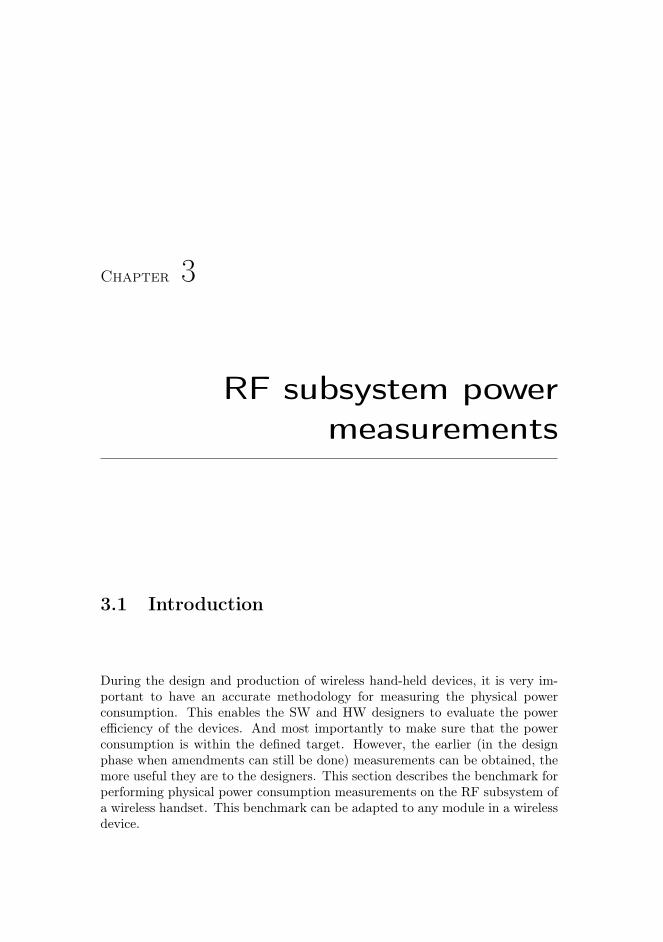
Chapter 3
RF subsystem powermeasurements
3.1 Introduction
During the design and production of wireless hand-held devices, it is very im-portant to have an accurate methodology for measuring the physical powerconsumption. This enables the SW and HW designers to evaluate the powerefficiency of the devices. And most importantly to make sure that the powerconsumption is within the defined target. However, the earlier (in the designphase when amendments can still be done) measurements can be obtained, themore useful they are to the designers. This section describes the benchmark forperforming physical power consumption measurements on the RF subsystem ofa wireless handset. This benchmark can be adapted to any module in a wirelessdevice.

46 RF subsystem power measurements
3.2 The power measurement Setup and proce-dure
This section describes the measurement setup and the procedures taken to per-form the power measurements.
3.2.1 The Hardware
The configuration of the physical power consumption measurements setup isshown in Figure 3.1.The setup is made up of the following components:
• Data acquisition device in form of the NI USB 6351;
• Work station with 2 SW tools;
– The tracing tool from which Tx and RX operations are scheduled;
– The data logging tool that interfaces to the data acquisition device;
• The resistor R [0.1Ω 5W ], that is inserted in the power supply line of themodule of interest. The voltage difference over this resistor is used tocalculate the power consumption of the module of interest;
• The trace box, that retrieves modem traces from the XTI port of themodem platform;
• The signal and spectrum analyzer connected to the antenna port of theDUT to measure the power of the outputted RF signal.
3.2.1.1 The configuration
A trace is cut on the power supply line of the RF subsystem and a 0.1Ω resistorinserted. A wire from each side of the resistor is connected to a measurementchannel of the NI USB instrument which is connected to the work station viaa USB port. The workstation is connected to the trace box via TCP/IP orUSB. A XTI cable connects the trace box and DUT. The signal and spectrumanalyzer is connected to the DUT by a coaxial cable. The triggering signal isrouted from the modem platform GPIO General Purpose Input Output to NIUSB and signal analyzer.

3.2 The power measurement Setup and procedure 47
NI USB (mV) Ampere meter (mA) Calibrated R (Ω) Div. %9.3787 98.1 0.0956 4.4103.599 104.1 0.0995 0.489.4 98.1 0.0958 4.17
Table 3.1: The calibration of the measurement resistor. The calibrated resis-tance is R = V/I where the V is the voltage difference and I thecurrent measured on the NI USB and ampere meter respectively.
3.2.2 Instruments calibration
The calibration validity of the signal analyzer, power supply and NI USB hasto be verified by checking the calibration stickers. The resistor R has to becalibrated and the attenuation associated with the coaxial cable connecting theDUT and the signal analyzer has to be defined. The resistor is calibrated usingthe setup in Figure 3.2. An ampere-meter is inserted in the path of the currentflow. Three measurements were conducted where the measured current andvoltage difference and the calibrated resistance are tabulated in Table 3.1.
The maximum divergence from the factory resistance of 0.1Ω is 4.4% whichis within the 10% tolerance of the resistor. The attenuation associated withthe coaxial cable is measured by a power sensor and a signal generator in thefollowing steps:
1. Generate an RF signal at frequency of interest at a reasonable power level;
2. Take 2 measurements, one when the power sensor is connected directly tothe output of the signal generator and the other when the coaxial cable isconnecting the power sensor and signal generator;
3. Compute the difference between the two measurements. The differenceindicates the attenuation associated with the coaxial cable.
3.2.3 SW configuration
In order to guarantee synchronous measurements, a trigger is used to start thelogging of power consumption and RF signal power. A triggering signal atthe start of the Tx scheduling operation is assigned to a GPIO on the modemplatform. This signal is connected to both the NI USB instrument and thesignal analyzer. These instruments are configured to start logging when everthe trigger signal is high.

48 RF subsystem power measurements
3.2.4 Measurement procedure
Preliminary procedures:
1. Warm up,The power supply and signal analyzer are required to be warm up for 30minutes. The NI USB only requires 15 minutes thus, the measurementsetup is left to warm for 30 minutes after power up;
2. Allow the phone to warm up by turning the transmitter to maximumpower for 5 minutes. This is in correspondence with the warm-up usedprior to conducting the TRP(Total Radiated Power) test [71].
The measurements:The power consumption of the RF subsystem is measured through the followingprocedures:
1. Parameter selection,the GUI, Figure 3.3, is used to select the parameters of interest. Theparameters of interest in this work are boxed in red. The Tx button isinvoked to start a tx operation;
2. Data acquisitionsthe triggering signal initiates the logging of the RF signal power (Tx power)and power consumption. Both the signal analyzer and Labview are set toaverage over 1000 subframes (1000 milliseconds).
However, this procedure is applicable for a limited number of measurements dueto the work load associated with conducting these measurements. In case of afull characterization, an automated approach is applied. This setup is shown inFigure 3.4 where:
• The chamber control engine provides access and ability to set the chamberto the desired ambient temperatures, the chamber returns the time towhen the desired temperature is reached;
• In the desired ambient temperature, phocom provides access to the DUTwhere commands can be sent to the UE, and for commands where powerconsumption is desired;
1. The FSV control allows the reading and reporting of the signal char-acteristics at the antenna port;
2. The NI executable is called for measuring the power when desired.

3.2 The power measurement Setup and procedure 49
3.2.5 Power consumption uncertainty/precision
The measurement system is affected by the systematic and random errors arisingduring the measurement process [72]. The systematic errors are referred to asmeasurement/instrumental uncertainties and are provided in the manufacturer’sspecifications for the devices in Figure 3.1 as:
• Voltage supply device (0.05% + 10mV) [73];
• Measurement resistors (10% and 1%);
• NI USB 6351 (reading × gain error + 10 × offset error + noise uncertainty)[74];
• Signal analyzer (0.39dB) [75].
The instrumental uncertainties above are modeled using intervals [76]. The re-sultant RF subsystem power consumption is thus represented in form of intervalsspecified by lower and higher bounds:
[P P ] = [V V ]× [Vd Vd]× [1
R
1
R] (3.1)
where V is the voltage of the source, Vd the voltage measured across the resistorR and the underlines and overlines as in V&V indicate the lower and higherbounds of the variable V .
The random errors caused by unpredictable variations in the measurement sys-tem are eliminated by having the same starting point (trigger) of the measure-ments and averaging over 1000 subframes for each power consumption measure-ment.
In practical terms, the system and random errors impact the spread knownin statistics and referred to as the precision/uncertainty in this work. Thetheoretical explanation of precision/uncertainty is depicted in Figure 3.5.
Due to the fact that the calculated precisions do not take into account the phys-ical environmental variables as the ambient and junction temperatures whichdo have an effect on the measurement process, these precisions may not reflectthe reality of the measurement process. Consequently, the DUT was invokedto transmit 100 LTE sub-frames 1000 times using a 20 MHz bandwidth at a23 dBm transmission power. This was conducted for ambient temperatures of−100C, 220C and 550C. The histograms, shown in Figure 3.5, for each of theambient temperatures represent the spread or precision to be expected at therespective ambient temperatures.

50 RF subsystem power measurements
3.2.6 Evaluation of the measurement system and method-ology
In order to verify the measurement methodology, three independent data sets ofthe RF subsystem power consumption measurements with the same operationalparameters (bandwidth, modulation and carrier frequency) as a function of Txpower where conducted. Each set of measurements created a buffer zone or offsetwhose offset parameter corresponds to the absolute value of the measurementuncertainties as shown in Figure 3.6 (only last box is shown here). Given thethree buffer zones, of independent measurement uncertainties in Figure 3.6,we do have a union and an intersection of the measurements. The Hausdorffdistance [77] is used verify how the two sets (union and intersection) differ fromeach other. The Hausdorff distance measures the similarity of two non-emptycompact sets in respect to their position in the metric space. This distanceindicates the extent to which each point in the union set is located relative to thepoints in the intersection set [77]. For a perfect match between measurements,the Hausdorff distance is 0 which would only occur in an ideal setup.
The Hausdorff distance
dH(∪Inj=1
,∩Inj=1
) = max supx∈∪
infy∈∩
d(x, y), supy∈∩
infx∈∪
d(x, y) ,
where sup is the supremum and inf the infimum, between the intersection ∩ andunion ∪ of the measurement uncertainty boxes is depicted in Figure 3.6. TheHausdorff distance is the length of the straight line segment joining the unionand intersection interval boxes at the top right of Figure 3.6 and is found to be0.31. The value is acceptable for our purposes but can be reduced in severalways. The simplest and least expensive is to replace the resistor in Figure 3.1by one with tighter tolerance.
3.3 Summary
This chapter has presented the measurement approach applied in the researchfor measuring the power consumption of the RF subsystem when transmittinga LTE signal. The precision/uncertainty in the measurement system has alsobeen presented at a room and extreme temperatures. The next chapter analyzesapproaches for modeling the power consumption of the RF subsystem.

3.3 Summary 51
DUT
RF+HPA Power supply line
Trace
box
Ethernet
Trace Tool:
Sends and recieves
messages from the
DUT
LabView:
Displays the
measured power
Workstation
R
Signal and spectrum
analyzer
XTI
NI USB
6351
Power supply
Tx -
power
modem PMIC
Power
management IC
V1
V2
Trig
gering
sig
nal
Figure 3.1: Power measurement setup used for the measurements in this work.The workstation forces the DUT into a specific mode of operation.During the operation, the DUT power consumption is measured byNI USB and displayed in LabView. The signal analyzer measuresthe output Tx power at the antenna port.

52 RF subsystem power measurements
DUT
NI
USB
Work
station
Ampere
meter
Resistor
Figure 3.2: The setup used for the calibration of the measurement resistor.The ampere meter measures the current drawn and the NI USBmeasures the voltage.
Figure 3.3: The interface “RF GUI” from which the desired RF subsystem- baseband logical interface parameters are selected. When theTx button is invoked, the DUT continuously transmits a signalgenerated using the selected logical interface parameters.

3.3 Summary 53
Automation script
Phocom
Ni
executable
FSV control
Chamber
control
Work station
DUT
GBIP
NI USB USB
Musti XTI
Ethernet
Temperature
chamber
Figure 3.4: The setup for automated power measurements. The FSV, DUT,temperature chamber and NI USB are controlled from the workstation.
Figure 3.5: The precision in the measurement process.

54 RF subsystem power measurements
0.042 0.0425 0.043 0.0435 0.044 0.0445 0.045 0.04550
50
100
150
200
250
300
350
400
450
500
Current (A)
Mea
sure
men
ts
(a) The distribution of the power consumption at the ambient temperature of −100C.,
0.044 0.0445 0.045 0.0455 0.046 0.0465 0.0470
100
200
300
400
500
600
700
Current (A)
Mea
sure
men
ts
(b) The distribution of the power consumption at the ambient temperature of 220C (labora-tory temperature).
,

3.3 Summary 55
0.0475 0.048 0.0485 0.049 0.0495 0.05 0.0505 0.0510
100
200
300
400
500
600
700
800
900
Current (A)
Mea
sure
men
ts
(c) The distribution of the power consumption at the ambient temperature of 550C.,
Figure 3.5: The distributions of power consumption at ambient temperaturesof −100C, 220C and 550C. The precisions, in terms of relativedifferences, for each of the ambient temperatures are 5.5%, 4.5%and 5.4% respectively.
,

56 RF subsystem power measurements
18 19 20 21 22 23 24 25
2
2.5
3
3.5
4
4.5
5
Tx power(dBm)
Pow
er(
w)
Power consumption Vs. Tx power at 10MHz 3 data sets
Data set1Set1 interval boxData set2Set2 interval boxData set3Set3 interval box
Figure 3.6: The buffer zones of three independent measurements used to cal-culate the Hausdorff distance.

Chapter 4
LTE RF subsystem powerconsumption modeling
4.1 Introduction
A power consumption analysis of a smartphone [4], the Openmoko Neo Freerun-ner, showed that the GSM modem consumes 80.6% of the total smartphonepower consumption (excluding the blacklight) for a GSM phone call. In thiswork, transmission mode power measurements on a LTE (Long Term Evolu-tion) modem have shown that the RF subsystem, in the worst case, consumes68% of the total smart phone power.
Consequently, the estimation of the RF subsystem power consumption beforethe mass production of wireless devices is absolutely vital. We presented an ap-proach for estimating the power consumption of the RF subsystem by the meansof emulation with a precision of 11% for a specific scenario [78]. The emulationmodel in this approach only took the logical interface parameter (between thebaseband and RF subsystem), Tx power, into account. It has been proven inthis work, through power measurements, that other logical interface parame-ters (bandwidth and carrier frequency) and a physical environmental parameter(temperature) also do have an impact on power consumption (see Table 4.1).

58 LTE RF subsystem power consumption modeling
Therefore, in this work, a new RF subsystem mathematical model that modelsthe power consumption for all possible scenarios at any ambient temperaturebetween −100C and 550C is presented. The possible scenarios are combinationsof the logical interface parameter values. The main originality in this workis the extension of the previous power emulation methodology [78] from two-dimensional space (one variable: Tx power) to fifth-dimensional space (logicalinterface parameters and temperature) keeping the uncertainty of the poweremulation within the uncertainty of the validation measurements.
4.2 Overview
4.2.1 RF subsystem power consumption emulation
A RF subsystem power consumption emulation methodology has been presentedin our published work [78] for a specific scenario where only a single RF subsys-tem power consumption affecting parameter (Tx power) was considered. Themethodology retrieves the logical interface parameters between the DBB (Dig-ital Baseband) and the RF subsystem from the XTI (X/Open Transport Inter-face)) port of the modem platform. The emulation model was computed as apolynomial interpolation using polynomial basis functions. This work analyzesmodeling approaches towards the most optimal approach capable of modelingthe RF subsystem power consumption as a function of all the relevant high leveland physical environmental parameters.
The FLPA (Functional Level Power Analysis) methodology was presented [79–81] for modeling the power consumption of the Systems-On-Chip (SoC). TheFLPA methodology consists of four steps:
1. A primary functional analysis describing the system as a grey box withhigh-level parameters having an effective impact on power consumption;
2. The device power profiling step, where power measurements are conductedfor the entire range of the defined parameters in order to determine theextent of the influence of the parameters on power consumption. Thisprovides the basis for the definition of the power relevant parameters.However, instead of conducting power measurements for the entire rangesof the defined parameters, in this work, we choose to define the lowerand higher bounds of these parameters in terms of power consumption.The influence of each parameters is computed as the relative difference ofthe power consumption as a function of the parameters’ higher and lower

4.3 FLPA analysis of the RF subsystem 59
bounds. This is much more effective than conducting measurements forthe entire ranges of the defined parameters;
3. The modeling of power consumption as a function of the relevant param-eters;
4. And finally the determination of the accuracy of the model.
The FLPA approach is adopted in this work for finding the power consumptionmodel of the RF subsystem. In this work, we are not only considering the high-level parameters but also a physical environmental variable (temperature). Thefour steps of the FLPA approach are analyzed with respect to the RF subsystempower consumption in the following sections.
4.3 FLPA analysis of the RF subsystem
In this section, we are applying a modified version of the FLPA analysis forfinding the most optimal approach for modeling the power consumption of theRF subsystem while transmitting a LTE signal.
4.3.1 Primary Functional Analysis
The primary functional analysis of the RF subsystem as a grey box with high-level parameters having an effective impact on power consumption was con-ducted and published in our previous work [78]. The major power consump-tions of wireless devices are largely functions of sequences of protocol/logicalactivities [78, 82, 83]. Hence, the power consumption of the RF subsystem isa function of the logical interface parameters between the RF subsystem andthe DBB. However, the physical environmental parameter, temperature, do alsoaffect the performance of the circuits and their effect is also investigated in thiswork. Heat emissions and temperature control on an electronic devices is knownto be highly correlated to power consumption [84]. The defined extreme temper-ature conditions −100 C and +550 C for the LTE technology [85] are consideredin this work. The logical interface [86] parameters from the LTE technologicalpoint of view are:
• Signal bandwidth ∈ 1.4, 3, 5, 10, 15, 20MHz;
• Modulation schemes QPSK (Quadrature Phase Shift Keying ), 16 and 64QAM (Quadrature amplitude modulation);

60 LTE RF subsystem power consumption modeling
• TX power ∈ [−40, 23] dBm;
• Carrier frequency (depends on the supported LTE bands).
The RF subsystem power consumption is also dependent on the circumstancessurrounding the near-field of the DUT (Device Under Test). Any near-fieldsetup would have a different impedance between the antenna and PA (PowerAmplifier) [87]. Each impedance is associated with a different reflection coeffi-cient [88] and thus also a corresponding power consumption. In this work, thetransmitter is terminated in a 50Ω load. The effect of the near-field on thepower consumption of the RF subsystem is to be investigated in our proceedingwork.
4.3.2 Device power profiling
In our previous work [80], it was proven that the power consumption of anLTE RF subsystem is technologically dependent on the carrier frequency, signalbandwidth and transmission power (Tx power). For a comprehensive evalua-tion, we are also evaluating the influence of the ambient temperature. Thus, forthe power profiling of the RF subsystem, the individual influence for each of thetechnological high level and environmental parameters on the power consump-tion of the RF subsystem is examined in this section.
For carrier frequency, a single band (LTE band 7) covering 2500-2570 MHz wasconsidered. Our analysis of the carrier frequency is focused on the channel edgeswhich are defined as the lowest and highest frequencies of the carrier separatedby the channel bandwidth as in FC± BWChannel
2 where FC ∈ 2500 2570MHzand BWChannel = 20MHz [85].
We are not evaluating the power consumption for the full ranges of the definedpower affecting parameters as indicated in the FLPA approach. It is more effi-cient to define the lower and higher bounds of the parameters in power consump-tion terms, as shown in Table 4.1, and analyze the influence of the parametersin terms of the relative difference taken between the power at the lower andhigher bounds.
The lower and higher bounds of the carrier frequency do attract scrutiny. Forthe LTE bands used in this work, numerically the lower and higher boundswould be 2510MHz and 2560MHz. However, practically the lower and higherbounds depend on the tuning of the modules in the RF subsystem. Therefore,for an appropriate definition of the carrier frequency bounds, the evaluation ofthe power consumption within the bandwidth of each band is necessary. This
4.3 FLPA analysis of the RF subsystem 61
Parameter Lower bound Higher boundCarrier Frequency 2560MHz 2510 MHzBandwidth (BW) 1.4MHz 20MHzTx power -40 23Temperature (ambient) −100 C 550 C
Table 4.1: Parameters lower and higher bounds
is accomplished by sweeping through each band with 1.4MHz bandwidth asdepicted in Figure 4.1 for bands 7 and 3.
The fact that the consumed power has such a non-monotonic behavior as afunction of the transmitted power precludes using the transmitted power ashomotopy parameter in convex homotopies (such as linear homotopies).
The device power profiling assessment is achieved through the follow-ing three steps:
1. Measurements when the four high level parameters and the ambient tem-perature are set to their respective lower bound values (see first combina-tion in Figure 4.2);
2. Measurements when the four high level parameters and the ambient tem-perature are set to their respective higher bounds (see second to last com-bination in Figure 4.2);
3. Lastly, the influence of each parameter combination is computed by therelative difference between the measurements in 1 and 2. The results ofthe HW power profiling are presented in Table 4.2.
Parameter Relative difference (%)Tx power 75Bandwidth 3 (For 2560 MHz)Carrier frequency 4Temperature 20.2
Table 4.2: The device power profiling summary showing that Tx power has themost influence on the RF subsystem power consumption followedby the ambient temperature bandwidth and carrier frequency.
The influence of each of the parameters in Table 4.2 is depicted in Figures 4.3a,4.3b, 4.3c and 4.4. Figure 4.3a shows the significance of temperature on powerconsumption especially for Tx powers greater than 5 dBm. Nevertheless, the

62 LTE RF subsystem power consumption modeling
2510 2520 2530 2540 2550 25602
2.05
2.1
2.15
2.2
2.25
Frequencies (MHz)
Pow
er (
W)
Ambient temperature 230C
Ambient temperature −100C
(a) Band 7 power consumption sweep.,
1.71 1.72 1.73 1.74 1.75 1.76 1.77 1.78 1.79 1.82
2.5
3
3.5
Pow
er c
onsu
mpt
ion
(W)
Carrier frequencies (GHz) in band 3
1.71 1.72 1.73 1.74 1.75 1.76 1.77 1.78 1.79 1.818
19
20
21
Tx
pow
er (
dBm
)
Power consumptionTx Power (at antenna port)
(b) Band 3 power consumption sweep.,
Figure 4.1: The RF subsystem power consumption as a function of carrier fre-quency swept with a bandwidth of 1.4 MHz in LTE bands 7 and3. Figure 4.1a shows a power consumption sweeping of band 7at temperatures −100 and 230 C. Figure 4.1b shows a power con-sumption sweep of band 3 along with the measured Tx power atthe antenna port. These plots illustrate that the power consump-tion within the different bands can behave very differently.

4.3 FLPA analysis of the RF subsystem 63
Figure 4.2: The combinations for logical and environmental parameters usedfor device profiling.

64 LTE RF subsystem power consumption modeling
temperature is not correlated to the bandwidth as shown in Figures 4.3b and4.3c. In regards to the carrier frequency, the power consumption can behavedifferently from band to band as shown in Figure 4.1. Figure 4.4 shows therelationship between carrier frequency and temperature. It can be observedthat the temperature effect on power consumption is homogeneous over thecarrier frequency bands.
4.3.2.1 Training and validation sets
Table 4.2 shows that the Tx power has the biggest impact on the RF subsystempower consumption. Thus, the training and validation sets were conducted as afunction of Tx power. The training sets consists of the power consumption foreach combination of the lower and higher bounds of the ambient temperature,carrier frequency and signal bandwidth as a function of Tx power taken at 1 dBmresolution. The validation set was conducted as a function of the parameters:
• Four carrier frequencies in band 7 (2510, 2528, 2548 and 2560 MHz);
• Ambient temperatures −100, 250 and 550C;
• Signal bandwidths (1.4, 5, 10, 15, 20MHz);
• Carefully chosen Tx power (-20, -10, 1, 5, 9, 13, 17, 21dBm).
The measurements are conducted by an automated setup (Figure 4.5) and theprocedure is as follows:
1. 3 training and validation sets in room temperature (250C). The DUT iscooled down for 10 minutes between each measurement set. It has beenverified through our own experiments that the DUT takes 10 minutes toacclimatize to room temperature and 30 minutes to get to the extremetemperatures;
2. The temperature chamber is set to −100C. The chamber returns theestimated time to reach the set temperature and the measurements arestarted after this time plus 30 minutes for acclimatization. Here, 3 trainingand validation sets of measurements are conducted;
3. The chamber is cooled down in 30 minutes and the procedure in 2 isconducted for 550C.

4.3 FLPA analysis of the RF subsystem 65
5 10 15 20
0.8
1
1.2
1.4
1.6
1.8
2
2.2
Tx power (dBm)
Pow
er(W
)
550C lower bound
550C higher bound
550C measured
−100C lower bound
−100C higher bound
−100C measured
(a) Power consumption as a function of ambient temperatures of 550 C and −100 Cwhile transmitting a 20 MHz bandwidth LTE signal.
,
16 17 18 19 20 21 22 23
1.4
1.5
1.6
1.7
1.8
1.9
2
2.1
2.2
2.3
Tx power (dBm)
Pow
er(W
)
20 MHz lower bound20 MHz higher bound20 MHz measured1.4 MHz lower bound1.4 MHz higher bound1.4 MHz measured
(b) Power consumption as a function of the LTE signal bandwidth at an ambienttemperature of 550C.
,
Figure 4.3: Power consumption as function of temperature continued on thenext page...

66 LTE RF subsystem power consumption modeling
16 17 18 19 20 21 22 23
1.2
1.3
1.4
1.5
1.6
1.7
1.8
1.9
2
2.1
Tx power (dBm)
Pow
er(W
)
20 MHz lower bound20 MHz higher bound20MHz measured1.4 MHz lower bound1.4 MHz higher bound1.4 MHz measured
(c) Power consumption as function signal bandwidth at −100C.,
Figure 4.3: The influence of temperature on power consumption for signalbandwidths 1.4 and 20 MHz is depicted. Measurements in Fig-ures 4.3a, 4.3b and 4.3c are measured at a carrier frequency of2560MHz. The Tx power range is chosen for better visibility butmeasurements were conducted for the full Tx power range [-4023] dBm (this regards all corresponding figures plotted as a func-tion of Tx power).

4.3 FLPA analysis of the RF subsystem 67
0.8 1 1.2 1.4 1.6 1.8 2 2.2 2.4 2.62
2.2
2.4
2.6
2.8
3
3.2
3.4
3.6
3.8
Carrier frequency (GHz)
Pow
er(W
)
−100C lower bound
−100C higher bound
−100C measured
550C higher bound
550C lower bound
550C measured
Figure 4.4: Power consumption as a function of frequency measured at ambi-ent temperatures of −100C and 550C while transmitting a 20MHzsignal at 23 dBm.

68 LTE RF subsystem power consumption modeling
Figure 4.5: These devices are cabled to the work station that automaticallyconducts power measurements. The DUT is controlled via thetracing device to perform transmitting operations. For each op-eration, a NI National Instruments Labview executable is calledthat records the consumed current.

4.3 FLPA analysis of the RF subsystem 69
4.3.3 The power consumption modeling
In this section, the multivariate modeling approaches below are introduced andapplied for modeling the power consumption of the RF subsystem:
• Multivariate polynomial fitting;
• Neural Networks;
• Homotopy continuation .
4.3.3.1 Multivariate polynomial fitting
The RF subsystem power measurements as a function of the Tx power in-creases exponentially for each of the power relevant logical interface param-eters, bandwidth and carrier frequency, as shown in Figure 4.3. The powerconsumption as the function of the logical interface parameters is therefore amultivariate polynomial surface known at the measured points. A functionf(w1, ..., wm, c0, ..., cp−1) =
∑p−1k=0 ckϕk(w1, w2, ..., wm) that models the power
consumption can be constructed [89, 90] where p is the number of elements inthe polynomial of m variables, w the function variables and c the polynomialcoefficients. Without loss of generality, for a second-order bivariate polynomialmodel [91], f(·) becomes:
f(w, c) = cTϕ(w) (4.1)c = [c1, c2, ..., c6]
T
ϕ(w) = [1 w1 w2 w21 w2
2 w1w2]
Given m > K data points from a training data set P where K is the numberof elements in f(w, c), the coefficients c can be computed as c = (ΦTΦ)−1ΦTPwhere Φ ∈ Rm×K is the Jacobian matrix of ϕ(x) [91]:
Φ =
1 w1,1 w2,1 w21,1 w1,1w2,1 w2
2,1...
......
......
...1 w1,m w2,m w2
1,m w1,mw2,m w22,m
However, the m variables, Tx power, signal bandwidth and carrier frequency,affecting the RF subsystem power consumption are of different lengths and theJacobian matrix of Φ(x) cannot be used for the computation of the coefficients

70 LTE RF subsystem power consumption modeling
c. Thus, for a second-order bivariate polynomial of variables of lengths M andN , Φ′ ∈ R(M×N)×K for the variables bandwidth B1,...M and Tx power T1,...,N
is constructed as:
Φ′ =
Bd1 · · · B1 B1T1 T d
1 · · · T1 1Bd
2 · · · B2 B2T1 T d1 · · · T1 1
......
......
......
... 1Bd
M · · · BM BMT1 T d1 · · · T1 1
Bd1 · · · B1 B1T2 T d
2 · · · T2 1...
......
......
...... 1
BdM · · · BM BMT2 T d
2 · · · T2 1...
......
......
...... 1
BdM · · · BM BMTN T d
N · · · TN 1
.
In polynomial fitting, the optimization finds the degree d for Φ′ that satisfiesthe targeted accuracy. For the scenario where the RF power consumption isa function of the Tx power and bandwidth, the multivariate polynomial modelwould be obtained as:
1. Construction of a multivariate matrix Φ′ of degree d. Start with d = 1;
2. Least squares fit to find the model c = (Φ′TΦ′)−1Φ′TP [89, 90];
3. Evaluation of the model against an independent set of data Pt. If thedesired precision is not met, the degree d is increased and iterate fromstep 1. The desired precision must be less than or equal to the uncertaintyin the measurement setup.
4.3.3.2 Neural networks
The accuracy of an approximation depends on the density of the observationpoints in the input space [92]. The curse of dimensionality [93] makes theaccuracy of an approximation in high-dimensional spaces to require the samplesize to grow exponentially with the input dimension. With the neural networks,this is solved by not having the dimension visible in the convergence rate buthidden in a functional class [92]. Herein, continuous functions on [0 1]d arerepresented as additive superpositions of continuous one-dimension functions.

4.3 FLPA analysis of the RF subsystem 71
For a compactly supported function f with supp(f) ⊆ [0 1]d, define a functionalclass by [92]:
Cf =
∫Rd
|ω| |f(ω)|dω < ∞
where |f(ω)| denotes the Fourier transform of f . We have an approximation
fn(x) =n∑
i=1
ciσ(aTi x+ ti) + c0
of the compactly supported function f such that
||(fn − f)1[0,1]d ||2 ≤ 2√d Cf n−1/2
where σ(·) is the nonlinear sigmoid function whereby σ(x) → 1 as x → ∞ andσ(x) → 0 as x → −∞.
The neural networks have been utilized for modeling the RF subsystem powerconsumption at the system level of abstraction [22]. In this section, we examinethe performance of the neural networks at prototype level. In the transmissionmode of the RF subsystem, we do have a continuous power consumption functionP (t), as a function of Tx power, signal bandwidth, carrier frequency and ambienttemperature. The functional form of P can be defined as a 4 × 5 × 1 neuralnetwork [94] shown in Figure 4.6 with one hidden layer.
Given an independently measured data set Pt(t), the coefficients W (1) and W (2)
can be optimized towards a minimal error between Pt(t) and Pm(t). The outputPm(t) of the neural network is defined as:
Pm(t) =
M∑j=0
W(2)j Zj , M = 1...5, Z0 ≡ 1 (4.2)
Zj = σ
( d∑i=0
W(1)ji inputi(t)
), d = 1...4, input0 ≡ 1 (4.3)
where inputi is the combination of the logical interface parameters at time t. Thebias terms (input0 for the hidden and Z0 for output units) play an importantrole in ensuring that the network can represent general non-linear mappings[95]. The pivotal task in the neural networks is the optimization of the hiddenunits weights W (1) and the output weights W (2). The optimization is achievedthrough the minimization of the quadratic cost function (sum-of-squared errorsfunction in Equation 4.4) between the data set Pt and the modeled power Pm.
E(W (1),W (2)) =1
2
N∑n=1
Pm(inputn,W(1),W (2))− Ptn
2 (4.4)

72 LTE RF subsystem power consumption modeling
Tx power
Bandwidth
Carrier
frequency
Inputs
Power
Bias 1 1
hidden units
(P (t)) m
Temperature
Figure 4.6: Network diagram for the two layer neural network used for mod-eling the power consumption of the RF subsystem. The input,hidden and power variables are denoted by nodes and the weightparameters are denoted by links between nodes. The arrows showthe direction of the information flow through the network duringforward propagation. The output of the network is the modeledpower Pm(t).
Iterative schemes taking steps in the weight space that minimize the sum-of-squared error function are utilized for finding the optimum weights. In this work,we have evaluated the following non-linear optimization algorithms towards analgorithm with the least sum of squared errors:
• Gradient descent [94];
• Pseudo-Gauss-Newton [96];
• Conjugate gradient algorithms [97,98];
– Hestenes-Stiefel;– Fletcher-Reeves [99,100];– Polak-Ribiere.
It is worth noticing that the principal disadvantages of neural networks in mod-eling stem from the requirement of a suitable set of example data for network

4.3 FLPA analysis of the RF subsystem 73
training, and the potential problems which can arise if a network is required toextrapolate to new regions of the input space which are significantly differentfrom those corresponding to the training data [95]. This means that for anyof the parameters affecting the power consumption of RF subsystem, charac-terization for each combination should be conducted with the highest possibleresolution. Hence, 64 transmission powers, 7 signal bandwidths and 20 carrierfrequencies(assuming 5 supportable bands), 64× 7× 20 measurements.
4.3.3.3 Numerical methods using homotopy and interval analysis
An homotopy is a continuous deformation of geometric figures or paths or moregenerally functions: a function (or a path, or a geometric figure) is continuouslydeformed into another one [101]. Such functions or paths are then consideredequivalent: i.e., homotopic. Originally, homotopy was used as a tool to decideweather two paths with same end-points would lead to the same result of in-tegration. The use of homotopies can be tracked back to works of Poincaré(1881-1886), Klein (1882-1883), and Berstein (1910) [101].
A homotopy is defined as a continuous map between two continuous functionsin a topological space. A homotopy can, therefore, be viewed as a continuousdeformation. The use of deformations to solve non-linear systems of equationsmay be traced back at least to Lahaye (1934) [101].
A homotopy between two continuous functions f0 and f1 from a topologicalspace X to a topological space Y is defined as a continuous map H : X × [0, 1] →Y from the Cartesian product of the topological space X with the unit interval[0, 1] to Y such that
H(x, 0) = f0, and (4.5)H(x, 1) = f1, (4.6)
where x ∈ X . The second parameter of H, also called the homotopy parameter,allows for a continuous deformation of f0 to f1 [101].
Two continuous functions f0 and f1 are said to be homotopic, denoted byf0 ≃ f1, if, and only if, there is a homotopy H taking f0 to f1. Being homotopicis an equivalence relation on the set C(X ,Y) of all continuous functions from Xto Y.
We use homotopies in order to reconstruct the unknown function of the con-sumed power of several power influencing variables (logical interface parametersand the physical environmental variables) from the measured values obtained

74 LTE RF subsystem power consumption modeling
by fixing one variable (that will be used as homotopy parameter) and varyinganother variable (or possibly several other variables). In this way, we study theprojections of the graph of that function of the consumed power on lower dimen-sional spaces (usually two dimensional spaces) corresponding to limit values ofthe range of the RF subsystem power influencing variable used as homotopy pa-rameter (e.g. carrier frequency or temperature). The homotopies are specificallyvery strong in the modeling of continuous variables in our case the physical en-vironmental variable temperature. In the case of the temperature, a continuousmap H : X × [0, 1] → Y can be used to model the power consumption as a func-tion of temperature in the defined temperature range (−100C to + 550C) [85].The homotopy parameter λ would be set as λ = 0 and λ = 1 for the power con-sumptions at temperatures −100C and +550C respectively and all the powerconsumptions in this range are on the homotopy curve as λ goes from 0 to 1.
Interval analysis is a well-known method for computing bounds of a function,being given bounds on the variables of that function [76]. The basic mathe-matical object in interval analysis is the interval instead of the variable. Theoperators need to be redefined to operate on intervals instead of real variables.This leads to an interval arithmetic. In the same way, most usual mathematicalfunctions are redefined by an interval equivalent. Interval analysis allows oneto certify computations on intervals by providing bounds on the results. Theuncertainty of each measure can be represented using an interval defined eitherby a lower bound and higher bound or a midpoint value and a radius. Theuncertainty of the consumed power as a function of a variable (say bandwidth)can be represented by higher bound plot and a lower bound plot. The consumedpower in between the measured points can be interpolated linearly or by usingcubic splines. The theoretical assumption that the consumed power is mono-tonically increasing with respect to the defined power influencing variables istested by computing the intersection of the areas between the lower bound plotsand the higher bound plots corresponding to the limit values of the homotopyparameter. Types of homotopies:
1. Linear:H1 = (1− λ)f1 + λf2
2. Non Linear:H = (1− λ)αf1 + λαf2
(a) Linearly varying non-linear homotopy:
H = (1− λ)αf1 + λαf2
where α = aλ+ b, where a and b are real constants;

4.3 FLPA analysis of the RF subsystem 75
(b) Quadratically varying non-linear homotopy:
H = (1− λ)αf1 + λαf2
where α = aλ2 + bλ+ c, where a, b and c are real constants.
In the device profiling section, we found out that we have 4 influencing pa-rameters; Carrier frequency (fb7), Tx power (txp), temperature (T ) and signalbandwidth (BW ). Given that the Tx power has the most significant influence onthe RF subsystem power consumption, the Tx power has to be the running vari-able for each of the homotopies of the other parameters. Numerically, it’s alwaysthe input parameter with the widest range that is chosen as the running variablebut in our case, we also have to consider the practicality of the input parame-ters. Our target is the homotopy H7(txp, λbw, λfb7, λT ), explained below, thatcomputes the power consumption of the RF subsystem for any given Tx power,signal bandwidth, carrier frequency and temperature. This is achieved througha combination of homotopies for each of the power influencing parameters asillustrated here:
The homotopy continuation based computation of power consumption as a func-tion of Tx power and signal bandwidth at the lower bound of the carrier frequencyand temperature.
f1(txp) = P1(txp)BW,fb7,T
,
f2(txp) = P2(txp)BW,fb7,T
,
H1(txp, λbw)fb7, T
= (1− λbw)αf1(txp) + λα
bwf2(txp)
The homotopy continuation based computation of power consumption as a func-tion of Tx power and signal bandwidth at the higher bound of the carrier fre-quency and lower bound of temperature.
f3(txp) = P3(txp)BW,fb7,T
,
f4(txp) = P4(txp)BW,fb7,T
,
H2(txp, λbw)fb7, T
= (1− λbw)αf3(txp) + λα
bwf4(txp)
The homotopy continuation based computation of power consumption as a func-tion of Tx power and signal bandwidth at the lower bound of the carrier frequencyand higher bound of temperature.
f5(txp) = P1(txp)BW,fb7,T
,
f6(txp) = P2(txp)BW,fb7,T
,
H4(txp, λbw)fb7, T
= (1− λbw)αf5(txp) + λα
bwf6(txp)

76 LTE RF subsystem power consumption modeling
The homotopy continuation based computation of power consumption as a func-tion of Tx power and signal bandwidth at the higher bound of the carrier fre-quency and temperature.
f7(txp) = P3(txp)BW,fb7,T
,
f8(txp) = P4(txp)BW,fb7,T
,
H5(txp, λbw)fb7, T
= (1− λbw)αf7(txp) + λα
bwf8(txp)
H3(txp, λBW , λfb7)T
= (1− λfb7)αH1(txp, λbw) + λα
fb7H2(txp, λbw)
H6(txp, λBW , λfb7)T
= (1− λfb7)αH4(txp, λbw) + λα
fb7H5(txp, λbw),
H7
H7(txp, λbw, λfb7, λT ) = (1 − λT )αH3(txp, λBW , λfb7) + λα
TH6(txp, λBW , λfb7)Where:
λBW =BW − 1.4
20− 1.4(4.7)
λfb7 =fb7− 2510
2560− 2510(4.8)
λT =T + 10
55 + 10(4.9)
α = 1 (4.10)
4.3.4 Evaluation of the RF subsystem Power modeling ap-proaches
This section evaluates multivariate modeling approaches towards an approachwith the highest mathematical approximation accuracy [102, 103]. The eval-uation was conducted in Matlab using a floating-point relative accuracy of2.2204×10−16 [104]. The mathematical approximation accuracy is the closenessof agreement between the modeled and measured power consumption [72,105].
The accuracy is computed in terms of the relative error er which is between themeasured power P (validation data set) and the modeled power P i.e.
er =∥P − P∥∞
∥P∥∞(4.11)
accuracy = 1− er (4.12)

4.3 FLPA analysis of the RF subsystem 77
In interval analysis, each interval can be defined by a midpoint and a range.The midpoint being the most likely value of the real variable if nothing else isknown or assumed about the spatial distribution of the measures. Then, theuncertainty is the range divided by 2 and the relative uncertainty is half of therange of the interval divided by the midpoint value [106–108].
The absolute modeling target is to have the relative error er of the modelingapproaches to be less than or equal to the uncertainty/precision of the mea-surements [106]. The DUT was set to transmit 100 sub-frames 1000 times at23 dBm using 20 MHz signal bandwidth at three temperatures −100C, 250Cand 550C. The precisions 5.5%, 4.5% and 5.4% where obtained as the relativedifference in each of the measurements for ambient temperatures −100C, 250Cand 550C.
The modeling approach(es) that will prove to have the modeling errors withinthe measurement uncertainties will subsequently be tried on a “validation” pro-totype. This prototype is made up of the same platform as the prior but withdifferent RF subsystem design. The major difference is that the RF subsystemof the device used in the evaluation has a different power amplifier for Lowerfrequency bands as band 5, high frequency bands as band 3 and 1 and band 7.Meanwhile the device to be used for validation has a single power amplifier forall bands which means that this device should have different power consump-tion behaviors compared to the prior as it has to be tuned for all the frequencybands.
4.3.4.1 Multivariate polynomial performance
The evaluation of the power modeling capabilities of this approach started in3-dimensions for the RF subsystem power consumption as a function of sig-nal bandwidth and Tx power. The intention was to increase the dimension ifthe performance proved to be within our targets. However, the evaluation ofthe multivariate polynomial fitting in Figure 4.7 shows that this methodologycan reach a minimum sum-of-squared errors of 0.19 corresponding to a relativeerror of 5.9% before the Φ′ matrix got too close to becoming singular (hencedeterminant close to 0 making the Φ′ matrix invertible).
Thus given this performance, we can rule out the application of the multivari-ate polynomial fitting for the modeling of the power consumption of the RFsubsystem.
Finally, we have compared the relative error obtained using smoothing splinecurves, thin-plate spline surfaces and piecewise linear and cubic spline surfaces

78 LTE RF subsystem power consumption modeling
1.5 2 2.5 3 3.5 4 4.5 5
10
20
30
40
50
X: 4Y: 0.1931
Non−linear optimization algorithms for RF power modeling
Degree d
Qua
drat
ic c
ost f
unct
ion
1.5 2 2.5 3 3.5 4 4.5 5
20
40
60
80
100
X: 4Y: 5.908
Rel
ativ
e er
ror(
%)Quadratic cost function
Relative error(%)
Figure 4.7: The performance of multivariate polynomial fitting showing thatthis approach cannot get better than a quadratic cost functionvalue of 0.1931.
with our requirement of 4.5%. While the relative error obtained using smoothingspline curves (3,12%) and piecewise linear and cubic spline surfaces (2,78% forboth of them) are acceptable, the relative error obtained using thin plate splinesurfaces is not acceptable (7,76%). Even the most precise local polynomialinterpolation methods are outperformed by homotopy continuation (see below).
4.3.4.2 Neural network performance
The evaluation of this approach was initiated in 4-dimensions for modeling thepower consumption as a function of Tx power, signal bandwidth and frequency(only the lower and higher bounds of LTE band 7 were considered). As this ap-proach is based on taking iterative steps in the weight space towards the optimalweights, the performance of the non-linear optimization algorithms for the train-ing of the network in Figure 4.6 is depicted in Figure 4.8. The Pseudo-Gauss-Newton algorithm has the best optimization followed by Fletcher-Reeves, Polak-

4.3 FLPA analysis of the RF subsystem 79
50 100 150 200 250 300
0
10
20
30
40
50
60
X: 300Y: 0.2125
Iterations
Quadra
tic c
ost
function
Non−linear optimization algorithms for RF power modeling
Gradient
Pseudo−Gauss−Newton
Fletcher−Reeves
Hestenes−Stiefel
Polak−Ribiere
Figure 4.8: The convergence of non-linear optimization algorithms towards theminimum error between Pt and Pm. The Pseudo-Gauss-Newtonalgorithm converges towards the least error of 0.21 after 300 iter-ations.
Ribiere with the final sum-of-squared errors 0.21, 0.30 and 0.42 respectively.This experiment was conducted for the power consumption in 4-dimensions P4.
However, in the training of the neural network the weights W (1) and W (2),are initialized with pseudo-random values drawn from the standard uniformdistribution. Hence, for the evaluation of the performance of this approach, thetraining in Figure 4.8 was conducted 1000 times yielding the following averagerelative errors for each of the optimization algorithms ( see Table 4.3).
The results in the table above do show that the performance of the NeuralNetworks does’t fall within the uncertainty in the measurements. And thisis observed while considering only two carrier frequencies in band 7 and alsowithout taking the temperature into account. Thus, to the best of our knowledgeand understanding of the Neural networks modeling, the approach do not meetour targeted modeling error.

80 LTE RF subsystem power consumption modeling
Parameter Relative error (%)Gradient [51.8879, 77.5622]Pseudo-Gauss-Newton [6.2167, 11.8051]Fletcher-Reeves [6.8736, 15.5786]Hestenes-Stiefel [26.5198, 40.2193]Polak-Ribiere [8.2287, 9.8113]
Table 4.3: The average of the validation error for the optimization algorithmstaken over 1000 trials.
4.3.4.3 Homotopy continuation performance
The evaluation of the performance of the homotopy continuation mapping ap-proach initiated with 4-dimensional linear homotopy (H3(txp, λBW , λfb7, T ) andH6(txp, λBW , λfb7, , T )) with the intention of applying other types of homotopiesaccordingly in order to meet our target of the modeling error within the mea-surement uncertainty.
The validation parameters for homotopies H3 and H6 are:
• Tx powers 1, 9 and 17 dBm;
• Carrier frequencies 2528 and 2548 MHz;
• And signal bandwidths of 5 and 10 MHz.
The evaluation of the homotopies H3 and H6 against the validation measure-ments proved a maximum modeling error of 1.4% and 2.5% for the two homo-topies respectively.
Upon the successful modeling in 4-dimensions P4, we moved to 5-dimensions P5
for modeling the power consumption for any given Tx power, signal bandwidth,carrier frequency (here only band 7 considered) and ambient temperature inH7(txp, λbw, λfb7, λT ). H7 was evaluated against a validation set of measure-ments at carrier frequencies 2528 and 2548 MHz, signal bandwidths 5 and10 MHz and all Tx powers with 1 dBm resolution. The maximum relative(equation 4.11) error between the modeled power consumption andthe validation set is 3% which is within our measurement uncertainty. For visualization, Figures 4.9a and 4.9b show the homotopy continuation basedmodeling of the power consumption for signal bandwidths between 1.4MHz and20MHz and temperatures between −100C and +550C. The temperature model-ing of the power consumption for ambient temperature 250C while transmitting

4.3 FLPA analysis of the RF subsystem 81
at a carrier frequency of 2560 MHz with the signal bandwidth of 20MHz is shownin Figure 4.9c along with the corresponding measured power. Also shown arethe lower and higher bounds of the measured power at 250C and the measuredpowers at −100C and 550C to prove that the modeled power consumption iswithin the uncertainties of the measured power. Finally, Figures 4.10a and4.10b show the plot of two bivariate homotopy functions and their intermediatetrivariate homotopy continuation interpolation at the midpoint of the homo-topy parameter and a zoom of the previous plot as a function of Temperature,signal bandwidth and Tx power. Lastly, the homotopy modeling of the powerconsumption as a function of Tx powers while operating at a signal bandwidthof 10 MHz at a carrier frequency of 2548 MHz in an ambient temperature of250C is shown in Figure 4.9d along with the lower and higher bounds of themeasured power also proving that the modeled power is within the measurementuncertainties.
4.3.4.4 Modeling evaluation with a validation device
The numerical approach based on homotopy continuation has proven to have amodeling error within our measurement uncertainty. This approach was thusalso put to task to model the power consumption of another design with adifferent RF subsystem design. For a one to one evaluation between the twodevices, a test corresponding to Figure 4.9d, where power consumption wasmodeled as a function Tx power operating at a signal bandwidth of 10 MHzat a carrier frequency of 2548 MHz, was conducted. The performance of thehomotopy (H7(txp, λbw, λfb7, λT )) approach on a device with a different RFsubsystem design is shown in Figure 4.11 with a modeling error of 2%.
4.3.4.5 RF subsystem power model
The overall target in this work is to find the most accurate and efficient RF sub-system power consumption model to be applied in the power emulator of the RFsubsystem power emulation methodology introduced in [78]. In the evaluationof modeling approaches, the numerical approach homotopy continuation provedas the only one to have a modeling error within the measurement uncertaintyof the 5-dimensional P5 power consumption function. Even-though in our case,linear homotopy has been sufficient for both devices used in this work, therecan be cases where the modeling error can appear to be out of the uncertaintybounds of the measurements. In such cases, one would upgrade to nonlinearhomotopy and subsequently linearly varying nonlinear homotopy and quadrati-cally varying nonlinear homotopy if the prior also fails. In terms of performance,

82 LTE RF subsystem power consumption modeling
4 6 8 10 12 14 161
1.1
1.2
1.3
1.4
1.5
1.6
1.7
1.8
1.9
2
Tx power (dBm)
Pow
er c
onsu
mpt
ion
(W)
20 MHz15 MHz10 MHz5 MHz3 MHz1.4 MHz
(a) Homotopy based modeling of the power consumption for signal bandwidths between1.4MHz and 20MHz.
,
6 8 10 12 14 16 18 20 22
1
1.2
1.4
1.6
1.8
2
2.2
Tx power (dBm)
Pow
er c
onsu
mpt
ion
(W)
550 (C)
500 (C)
450 (C)
400 (C)
350 (C)
300 (C)
250 (C)
200 (C)
150 (C)
100 (C)
50 (C)
00 (C)
−50 (C)
−100 (C)
(b) Homotopy based modeling of the power consumption for ambient temperatures between−100C and +550C when transmitting a 20MHz LTE signal as a function of Tx power.
,
Figure 4.9: Homotopy based modeling continued on next page...

4.3 FLPA analysis of the RF subsystem 83
15 16 17 18 19 20 21 22 23
1.2
1.4
1.6
1.8
2
2.2
Tx power (dBm)
Pow
er c
onsu
mpt
ion
(W)
−100 (C) Measured
250 (C) Homotopy
250 (C) Measured
550 (C) Measured
250 (C) Lower bound
250 (C) Higher bound
(c) Homotopy based modeling of the power consumption as a function of Tx powerat signal bandwidth 20 MHz for the ambient temperature of 250C along withthe measured power with its lower and higher bounds. Also shown are the powerconsumptions for ambient temperatures −100C and +550C.
,
2 4 6 8 10 12 14 16 18
0.9
1
1.1
1.2
1.3
1.4
1.5
1.6
1.7
1.8
Tx power (dBm)
Pow
er c
onsu
mpt
ion
(W)
HomotopyMeasuredLower boundHigher bound
(d) The 5-dimensional homotopy modeling of bandwidth, frequency, temperatureand Tx power
,
Figure 4.9: The homotopy based modeling of the power consumption as afunction of bandwidth (Fig. 4.9a), ambient temperature (Fig. 4.9band Fig. 4.9d) and the 5-dimensional modeling for bandwidth,frequency, temperature and Tx power in Fig. 4.9d.

84 LTE RF subsystem power consumption modeling
(a) Plots of two bivariate homotopy functions and their intermediate trivariate homotopycontinuation interpolation at the midpoint of the homotopy parameter.
,
(b) Zoom of the preceding plot.,
Figure 4.10: Bivariate homotopy functions.

4.3 FLPA analysis of the RF subsystem 85
0 5 10 15 20
1
1.2
1.4
1.6
1.8
2
2.2
Tx power (dBm)
Pow
er c
onsu
mpt
ion
(W)
HomotopyMeasuredLower boundHigher bound
Figure 4.11: Evaluation of the homotopy approach on a device with a differentRF subsystem design.
this approach has proven to have an accuracy of atleast 97% ± 2.75% (consid-ering the worst uncertainty for the ambient temperatures) evaluated over twodifferent RF subsystem designs. For training, the approach requires eight sets ofmeasurements f1 . . . f8 (presented in section 4.3.3.3) as a function of Tx powertaken at a 1 dBm resolution (64 Tx power powers). For validation, a set of mea-surements for each ambient temperature,−100C, 250C and 550C is conducted.The measurements are conducted for four carefully chosen carrier frequencies(2510, 2528, 2548 and 2560 MHz in this case) for all the five operational sig-nal bandwidths as as a function of eight carefully chosen Tx powers. Thus,992 measurements are required for the training and validation of the homotopyapproach.

86 LTE RF subsystem power consumption modeling
4.4 Discussion
This work has focused on the modeling of the power consumption of an analogcircuit, the RF subsystem, for power emulation. The power emulation method-ology was introduced for digital circuits at the RTL level [66] and was proved ina feasibility study [18] to have a precision of 10%. However, the power emula-tion at the RTL level cannot be conducted for realistic scenarios as for the casewith the RF subsystem emulated at prototype level. Secondly, the accuracy ofthe emulated power at prototype level is only constrained by the accuracy ofthe mathematical approximation. Therefore, it is only advantageous for poweranalysis to also have a power emulation model of the digital circuits at proto-type level. The FLPA approach would also be utilized for the computation ofthe emulation model of the DBB.
4.5 Summary
We have in this work examined multivariate modeling approaches for an ap-proach that can model the 5-dimensional power consumption of the RF subsys-tem when transmitting an LTE signal. The RF subsystem power consumptionhas proven to be a function of the logical interface parameters Tx power, car-rier frequency and bandwidth and the ambient temperature. The numericalapproach based on homotopy continuation has proven to optimally conductthe functional mapping between the RF subsystem power consumption and thelogical interface between the baseband and the RF subsystem for the ambienttemperatures between the defined extreme cases. This modeling approach pro-vided a mathematical function approximation accuracy of 97% ± 2.75%. Theapproach was also tried on a device with a different RF subsystem design whereits power consumption was modeled with an accuracy of 98% ± 2.75%.
The emulation model obtained in this chapter is utilized in the next chapter toemulate the power consumption of the RF subsystem.

Chapter 5
LTE handset RF powerconsumption emulation
5.1 Introduction
The methodology for emulating the power consumption of the analog part (onlyTx) of the wireless modem, RF subsystem, when transmitting a LTE signal ispresented in this section. The architecture of the methodology is depicted inFigure 5.1. As mentioned in Chapter 4, the power consumption of RF subsystemis a function of logical and protocol related commands, the methodology listensthe logical interface between the DBB and RF system for these commands. The“parameter extractor” module extracts the carrier frequency, signal bandwidthand Tx power and forwards them to the “RF power emulator” that computesthe emulated power using a predefined mathematical model.
The emulated power is a product of a mathematical mapping between the logicaland protocol related commands and a predefined mathematical model. Themathematical model for any given RF subsystem design is obtained throughthe steps shown in the flow chart in Figure 5.2. The FPLA analysis is appliedon each RF subsystem design for the computation of the mathematical model.This was conducted in Chapter 4 where the homotopy continuation numericalapproach proved to meet our requirements for a power model. In this Chapter,

88 LTE handset RF power consumption emulation
1
or XTI
• Parameter extractor logs: • Logical interface parameters for each subframe,
• Setting time.
• RF power emulator • Computes the power using the predefined model
• Aligns the computed power to the setting times
Figure 5.1: The RF subsystem power emulation system, monitors the streamof the logical commands over the DIGRF interface, extracts theRF subsystem power dependent parameters in the “Parameter ex-tractor” module and computes the emulated power in the “RFpower emulator” module.

5.1 Introduction 89
the obtained model is put to task for emulating the power consumption of a reallife scenario though still in conducted mode. The real life scenario here is theactive connection while transmitting data. The power consumption of the reallife scenario is to be measured along with the logical and protocol commandsused for emulation. The measured and emulated powers are to be compared forreal life scenario validation of the model.
FLPA analysis Given a modeling
approach
Validation Model against
realistic scenarios
Meets accuracy
Choose a new
modeling approach
For every RF subsystem design
Power model
Emulation model
Power emulation
system
Tx power
Carrier frequency
Bandwidth
Ambient temperature
Near-field Emulated power
per subframe
(1ms)
No
Modem
platform
Figure 5.2: Emulation flow showing the process through which the emulationmodel of a RF subsystem is obtained.

90 LTE handset RF power consumption emulation
5.2 Power emulation model
The evaluation of the multivariate algorithms proved the homotopy continu-ation numerical approach to have a modeling error within the measurementuncertainty of the data in the training sets. The approach also proved to be theleast complex in terms of the number of mips and also requires the least numberof measurements for training. This approach takes the power consumptions ofthe lower and higher bounds of signal bandwidth, carrier frequency and ambi-ent temperature and maps the power consumption for all combinations of theseparameters as a function of Tx power. Thus, power consumption of each sce-nario is computed during the training phase and stored. Hence, a data matrixof dimensions 14 × 4 × 64 × 6 has the power consumptions of the RF subsys-tem for all combinations of the logical interface parameters signal bandwidth(6), carrier frequency (4), Tx power (64) and ambient temperatures (14). Herefor the temperature, 14 temperatures were chosen between the extreme con-ditions, [−100C 550C], whose power consumptions had an interval larger thanthe measurement uncertainty. Thus, the modeling of the power consumptionfor any given combination of logical/protocal parameters and temperature is anindexing task. Say, the RF subsystem power consumption when transmittingat a carrier frequency 2528MHz, using a signal bandwidth of 10MHz at a Txpower of 13 dBm in a room of 250C is H7(8, 2, 54, 3) where H7 is the homotopyfunction obtained in Chapter 4.
5.2.1 RF subsystem Power consumption emulation
The power consumption emulation system that takes the logical interface pa-rameters between baseband and RF subsystems, via XTI (X/Open TransportInterface), as inputs to compute the LTE sub-frame average power consumptionof a specific RF subsystem is depicted in Figure 5.1.
During runtime, modem SW traces containing the logical interface parametersfor each sub-frame are written to the XTI port in the Tx scheduling functionof the modem SW. The trace box, connected to the DUT via the XTI port,forwards the modem software traces to the work station (see Figure 5.3). Theoptimal emulation system would compute the emulated RF subsystem powerconsumption for each sub-frame in the modem SW and trace it out to the XTIport.
We have in this work chosen to work off-line where the modem SW traces areprocessed on the workstation for the extraction of the relevant logical interfaceparameters and then used for the computation of the emulated power. In order

5.2 Power emulation model 91
DUT
RF+HPA
Musti
box
Ethernetet
Trace Tool:
Sends and recieves
messages from the
DUT
LabView:
Displays the
measured power
Work station
R
System simulator
NI USB
6351
Power supply
DBB IC
PM IC
Figure 5.3: The power emulation validation setup using a system simulator.
to illustrate the computation of the emulated power in a semi-realistic scenario,the DUT is connected to a system (eNOB) simulator (see Figure 5.3). Thescenario in this experiment is referred to as semi-realistic because the DUT isconnected to the system simulator in conducted mode rather than the realisticradiated mode. The system simulator simulates the base-station (eNOB) whichinforms the DUT, among other items, which technological parameters to usefor transmissions (Hence, the carrier frequency, signal bandwidth, modulationscheme, Tx power and more). However, for our experiment, we defined thetechnological parameters in the system simulator that were invoked in the DUT.Here during the transmission of a LTE signal on carrier frequency 2528 MHzusing a signal bandwidth of 10 MHz, the following Tx powers (plotted in Figure5.4) were observed/measured:
• Requested Tx power: The Tx power requested in both local and normalmodes (semi-realistic scenario) of operations. In local mode, the requestedpower is invoked in the trace tool and in normal mode it is invoked in thesystem simulator;
• Logical Tx power: The Tx power from the logical parameters extractedduring normal mode;
• Measured Tx power in normal mode: The measured Tx power at theantenna port during the execution of the semi-realistic scenario;
• Measured Tx power in local mode: The measured Tx power at theantenna port during the training of the model in Local mode.

92 LTE handset RF power consumption emulation
Figure 5.4 depicts the requested Tx power, logical Tx power and the Tx powermeasured both in local and normal mode. The assumption in this work wasthat the Tx power measured at the antenna port would be in agreement forboth local and normal modes of operations. However, in our case here, we dohave a relative difference of 9% between the measured power in the two modes.This difference does also affect power consumption as the Tx power is the biggestcontributor to the RF subsystem power consumption. The Tx power measuredin local mode is on average 1.5 dBm lower than the requested power but stillwithin the defined ±2dB tolerance [52]. The difference in the Tx powers inthese two modes is related to the fact that in normal mode of operation, thereis a closed loop power control that pushes the UE to meet the requested power(if possible).
As indicated earlier that the modeling of the power consumption using thehomotopy approach is an indexing task, as the carrier frequency and the signalbandwidth are constant in this scenario, the emulated power is extracted asH7(8, 2, x, 3) where x is the logical interface parameter Tx power. However,since the homotopy is computed at 1 dBm resolution, we do interpolate linearly(f(x+ y) = f(x)+ y× (f(x+1)− f(x)), 0 < y < 1) between the integer valuesfor double logical interface parameter values.
The resultant emulated power along with the measured power, for validation,is depicted in Figure 5.5. The first intriguing point is the offset between themeasured and the emulated power. This is due to the fact that the emulationmodel is trained in local mode where only the physical layers are active contraryto normal mode when the entire modem is active.
It was expected that as it is only the Tx power that is changing in this scenario,the power consumption steps, from one Tx power level to another, in both theemulated and measured power consumption should be relatively the same. Theevaluation of power consumption between the lowest and highest Tx power,in Figure 5.5, yielded a relative difference of 16% between the emulated andmeasured power consumption. This difference, which was expected to be withinthe measurement precision of 4.5%, is definitely due to the fact that there ison average a 1.5 dBm difference between the Tx powers measured, in local andnormal modes, at the antenna port.
The accuracy of the emulation system is dependent on the closeness of theemulated power to the measured power consumption hence 84% ± 2.75% inour case. The emulation model applied has an accuracy of 97% ± 2.75% andthe emulation system accuracy was expected to also be around this accuracybut definitely not out of the range of the measurement precision. However, dueto the fact that we do have a Tx power tolerance of ±2dBm and also giventhe open loop power control during training in local mode, the measured power

5.2 Power emulation model 93
40 50 60 70 80 90
13
14
15
16
17
18
19
20
Time (sec)
Tx
pow
ers
(dB
m)
Requested Tx powerLogical Tx powerMeasured Tx power in NMMeasured Tx power in LC
Figure 5.4: The requested and measured Tx power for local (during training)and normal modes (semi-realistic scenario) of operations.
consumption (in local mode) P (txp) as a function of the Tx power txp is within[P (txp − 2dBm) P (txp + 2dBm)]. Hence, the expected worst case accuracyof the emulation system is computed below given the ±2dBm tolerance on Txpower.
Notations:
• Let EA stand for emulation accuracy;
• MA for mathematical approximation accuracy,;
• A for power consumption at Tx power -2 dBm, A = P (txp− 2dBm) (theTx power in both A and B are the measured values);

94 LTE handset RF power consumption emulation
0 2 4 6 8 10
x 104
1
1.5
2
2.5
Time (sec)
Pow
er c
onsu
mpt
ion
(W)
Emulated powerMeasured power
Figure 5.5: The measured and emulated power consumption while transmit-ting a LTE signal with ascending Tx powers. The start, step andstop Tx powers are 10, 1 and 20 dBm respectively.
• B for power consumption at Tx power +2 dBm, B = P (txp+ 2dBm);
• And P the power consumption as a function of Tx power.
EA = 100−((B −A)
B∗ 100 + (100−MA)
),
For the requested Tx powers between 10 and 23 dBm, we can expect the worstcase emulation system accuracy to be 69.31% ± 2.75%. Thus, the expected

5.2 Power emulation model 95
emulation accuracy is within [69.31%, 97%] ± 2.75% for worst and best cases.The worst case accuracies for the requested powers as a function of the measuredTx powers and power consumption P (txp) are plotted in Figure 5.6. The Tx
9 10 11 12 13 14 15 16 17 1868
70
72
74
76
78
80
82
84
86
88
X: 16.33Y: 69.31
Em
ulat
ion
accu
racy
(%)
Measured Tx power (dBm)
X: 17.98Y: 86.91
Figure 5.6: The expected emulation system accuracies as a function of themeasured Tx powers.
power range from 10 dBm is chosen because it is where the significant changes,in power consumption, between the Tx powers do take effect.
In summary, the capability for emulating the RF subsystem power consumptionhas been shown where in the worst case scenarios when the outputted Tx powerTxp ∈ txp − 2dBm, txp + 2dBm, the emulation accuracy can be as low as69.31%. However, this is very device dependent and relies upon the tuning andcalibration of the RF subsystem from device to device. The case was differentfor a device used early in this work [109] but it is not supported anymore.Figure 5.7 shows the emulation of the power consumption of the RF subsystem

96 LTE handset RF power consumption emulation
of this device where the relative difference between the power consumption atlowest and highest Tx powers is 4.55% for the emulated and measured powerconsumption during a realistic transmission scenario. In Figure 5.7, the offsetbetween local and normal modes has been omitted.
0 10 20 30 40 50 601
1.5
2
2.5
3
3.5
4
4.5
Time(sec)
Pow
er(W
)
RF power consumption emulation model validation
Emulated powerMeasured power
Figure 5.7: Emulation validation using a device from the early stage of theproduct development. The Tx power is ramped from -6 to 23 dBm.
Due to the dependence of the power control mechanisms used in local and nor-mal modes, the development of the emulation model can be conducted in twostages depending on the maturity of the device under design. In the early phaseof the design with only physical layer maturity, the emulation model would bedeveloped in local mode. Later in the design phase, when normal mode matu-rity is achieved, we would then develop a corresponding emulation model whoseaccuracy would only depend on the accuracy of the mathematical approxima-tion. The next section analyzes the practical use of the emulation system andthe feasibility of emulating the RF subsystem power consumption for field mea-surements.

5.3 Integration into the power management flow 97
5.3 Integration into the power management flow
This section explains the usage of the emulation system and how this method-ology can be integrated into the power management flow presented in Figure5.8 which consists of power estimation, emulation, measurements and validationfor the purpose of power consumption optimization. The power managementflow starts with the power estimations which generally depend on the empiri-cal knowledge mostly coming from experiences of previous devices. The poweremulation which has so far been only for digital devices is conducted when thehardware design and corresponding RTL code is made. At this point in thedesign of the chipsets, the first builds of the chipsets are manufactured but withminimal functionalities (physical layer functionalities). The physical layer func-tionalities are hence utilized to train the emulation model for the RF subsystemwhich is inserted in the power management flow. When the chipset functionalitymatures, physical power measurements for real life scenarios are computed andcompared to estimation and emulation values for validation. During the vali-dation, analyses of the divergences between the physical power measurements,estimation and emulation are made and utilized for optimizing the power esti-mation and emulation methodology.
The emulation of digital circuits using the RTL hardware design is limited tosimplified scenarios. This is mostly due to the requirement of the FSDB (FastSignal Data Base) file, used for computing the emulated power, that fills up toa Gb for just an attach procedure (45 seconds). Moreover, we do not have theRF subsystem in the emulation environment for digital circuits, its functionalityis simulated here.
Consequently, given the successful emulation of the RF subsystem power con-sumption for realistic scenarios early in the design process, this methodologyhas been evaluated for emulating the power consumption at modem level, thusfor the entire modem platform. The study was conducted in our work presentedin [110] where the FPLA approach was applied to find the mathematical modelof the modem power consumption with an accuracy of 94.81% ± 2.75%.
We have also evaluated the feasibility of applying this methodology to the em-ulation of the SAR induced while transmitting from a device using our modemplatform. The principles of the FLPA approach are also applied though simu-lation measurements are accurate enough to be used instead of physical mea-surements as presented in [27, 68, 69]. We have not been able to conduct SARsimulations and measurements in the course of this work. However, accord-ing to the published work, the high level parameters influencing SAR are themeasurement parameters in the SAR measurement protocols defined by IEEEStd 1528-2003 [24]. These parameters include, antenna type, carrier frequency,

98 LTE handset RF power consumption emulation
transmission bandwidth (if it exceeds more than 1% of the carrier frequency),output power and the distance between head and antenna.
5.3.1 Extrapolation to field measurements
The target of this work is to estimate the RF subsystem power consumptionof wireless devices in real life scenarios at an early stage of the productionprocess for the purpose of optimization. The emulation process of the powerconsumption conducted in the lab can also be applied on field measurementsand scenarios given the logical interface parameters captured during the fieldtestings. The power consumption estimate of the RF subsystem of the DUT,for a FTP upload scenario when the DUT is in motion, is obtained through thefollowing steps:
1. Flash an existing mature LTE wireless device with the modem SW usedby the DUT for computing the emulation model;
2. Connect the device to a trace box or insert a SDcard on which traces canbe dumped, start logging the modem SW traces and connect the deviceto a cellular network;
3. Put the device in a car, start driving and conduct an FTP upload;
4. Extract the traces and conduct the homotopy H7(txp, λbw, λfb7, λT ) =(1− λT )
αH3 + λαTH6 for the emulated power plotted in Figure 5.9.
Even though the prototype (DUT) used for training the emulation model isnot capable of conducting a FTP upload, the emulated power gives an estimate(with a known accuracy) of it’s power consumption for a FTP upload in motion.Thus, with this methodology, we can have an insight in the RF subsystem powerconsumption for all scenarios of interest given the modem SW traces. However,the training model is a 50Ω system while in the field with the antenna on, itis anything else except 50Ω. Therefore, the power consumption in the field isexpected to be relatively higher due to the impendence changes that lead tohigher reflection coefficients. The reflection coefficient and power consumptionare expected to be positively correlated because the RF subsystem would try tocompensate for the reflected power by increasing the Tx power.

5.4 Discussion 99
5.3.2 Power consumption optimization
The target of power management is the ability of identifying and justifying hotspots. For any given scenario of the chipset, idle, call, max throughput, etc, wedo have a power budget. Thus, when the emulation model has been trained,modem traces containing the logical interface parameters are used to emulatethe power consumption of each scenario of interest. This provides us with theidea about how far the DUT under design is from the budgeted power. For theanalysis, we would scrutinize the emulated power curve as a function of time toidentify unusual behaviors. The unusual behaviors can be optimally identifiedby comparing the emulated curve to a reference curve of a previously poweroptimized chipset.
5.4 Discussion
In summary, this work has presented a new emulation methodology for theanalog RF subsystem in a portable device, focusing on the LTE transmitter. Theemulated power is computed as a function of the logical interface parametersand the ambient temperature using a predefined mathematical model. Themathematical model was proven to have an accuracy of 97% ± U where U ∈2.75%, 2.25% and 2.7% for temperatures −100C, 250C and 550C, and wasobtained using linear homotopy continuation.
The emulation method and results presented here focus on the RF transmit-ter portion because, historically, the PA was the largest power consumer in aportable device. However, in the newest smart phones, such as e.g. the Sam-sung Galaxy S III and its predecessor [111], dual and quad core GHz/s speedprocessors required for high-data rate applications start dominating the powerconsumption and heat removal requirements. The power consumption of theseprocessors can be emulated by power estimation tools such as PowerTheater [15]given their RTL codes. This approach applied to realistic scenarios would haveenormous memory requirements, and thus is inefficient. The approach presentedin this paper can also be applied to the emulation of power consumption of theapplication processors under realistic operational scenarios.

100 LTE handset RF power consumption emulation
1
Power
Estimation
Power Emulation
Digital designs
RTL/
gatelevel
Analog designs
RF subsystem
power
emulation
Physical power measurements
Po
we
r ma
na
ge
me
nt flo
w
Validation
Figure 5.8: The power management flow from the design of the chipsets to theproduction.
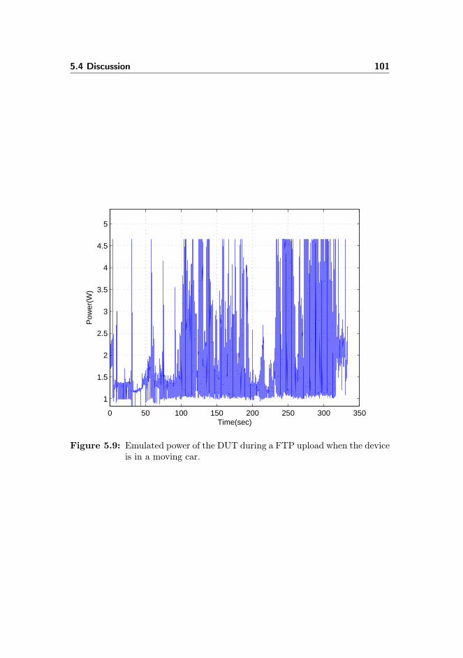
5.4 Discussion 101
0 50 100 150 200 250 300 350
1
1.5
2
2.5
3
3.5
4
4.5
5
Time(sec)
Pow
er(W
)
Emulated power for Field testing "FTP upload in movement"
Figure 5.9: Emulated power of the DUT during a FTP upload when the deviceis in a moving car.

102 LTE handset RF power consumption emulation

Chapter 6
Conclusions
6.0.1 Introduction
This chapter is presenting the problem domain, results and future work of theresearch conducted in this thesis.
6.0.2 Problem domain
The problem domain of the research in this work laid in the desire for Nokiato produce mobile devices with low power consumption and minimized electro-magnetic radiation induction for users. The low power and radiation in themobile devices is traced to the transmission process of data to the cellular net-work where the wireless modem plays a major part. Given the fact that thetarget technology of the research was LTE whose core objective is high speedcellular data transmission and also that the transmission process is one of thehighest power consumers, the research narrowed down to the transmission partof the cellular device. Hence, approaches towards low power consuming digi-tal baseband and RF subsystem of the wireless modem were in question. Lowpower design requires accurate power estimations/emulations during the designphase where hot spots can be identified and dealt with. Emulation approachesfor digital circuits are available with accuracies of up to 90% but not for analog

104 Conclusions
circuits which the RF subsystem is composed of. Thus, the research focusedon an emulation approach for the analog part of the transmission chain of thewireless modem.
The RF subsystem forwards the RF signal to the antenna for transmission whichimplies that the input parameters for power emulation of the RF subsystem alsoto do have an impact on the electromagnetic radiation generated for transmittingthe RF signal. This hypothesis was also investigated in this research.
6.0.3 Results of the research
The methodology for emulating the power consumption of the RF subsystemwhile transmitting a LTE signal has been presented in this work. The method-ology evolves from physical power measurements on the first builds of the targetand utilizes prior recorded logical interface parameters of scenarios of interest toemulate the power consumption. The measurements are used for characterizingand computing the power emulation model of the DUT.
Ambiguity is raised by the fact that physical measurements are made on thetarget and therefore the purpose of the emulation methodology can seem trivial.The physical measurements are conducted on the first builds of the target withonly physical layer functionality and thus without the possibility of measuringthe power consumption for the high level scenarios as max data throughput andFTP uploading.
The methodology presented in this work provides an estimation of the powerconsumption of the device under design for all scenarios of interest given thelogical interface parameters recorded during the execution of these scenarios.It is to be noted that the logical parameters are recorded on a mature devicerunning on the same SW as used for the characterization.
The accuracy of the chosen emulation model has been proved up to 97% ±2.75% but the accuracy of the emulation methodology is highly dependent onthe tuning of the devices in the RF subsystem given the tolerance on the Txpower. Experiments in this work have proven emulation accuracies of 84% ±2.75% and 94.3% ± 2.75%. It has also been proven for the device used inthis work that the worst case accuracy when the Tx power is on the edges ofthe defined tolerances can be as low as 69.9% ± 2.75% which is an acceptableaccuracy of an estimate.

105
6.0.4 Future work
The successful prove of concept of the power emulation methodology applyingthe FLPA approach for computing the emulation model has motivated the ap-plication of the methodology to the full wireless modem. The emulation of themodem power consumption during transmission has been introduced and theemulation of whole transceiver operations is the next target.
The RF subsystem and digital baseband emulation methodology that has sofar focused on the uplink direction is going to be extended to cover the wholebaseband and RF subsystem transceiver operations. Herein, the baseband andRF subsystem receiving operations are also to be characterized and modeled.
The methodology introduced in this work is to be applied to target devices as cellphones when the modem has gained full functionality. Though measurementscan be conducted here, full scale physical power measurements for durationsof several hours are not possible and so are the 2-dimensional measurementsduring field tests. Here, the emulation methodology is going to play a big role.
This work also looked at the possibility of emulating the SAR based on sim-ulations and measurements in published work. The characterization and sub-sequently the emulation of the SAR of the target device having our modemplatform is in planning at the Department of Electronic Systems at AalborgUniversity.

106 Conclusions

Appendix A
Appendix
A.0.5 CMOS WCDMA transmitter performances

108 Appendix
Performance crite-ria / architecture Homodyne [37] Homodyne [38] Homodyne [39]Technology 0.35µm CMOS 0.18µm CMOS 90nm CMOSFrequency range 1920 - 1980 MHz centered at 2.0626 centered at 1.7GHzDynamic range 50dB N.A N.A
Maximum output power 6dBm
0dBm at 2GHz6dBm at 1db com-pression point at2GHz 9.6dBm
Spurious(all band) < -80dBm N.A N.A
ACPR 38dB at 1.92MHz
-35dBc at 5MHzofset -50dBc at10MHz offset -43.2dBc at 5MHz
Power dissipation 363mW at 3.3V 223mW at 1.8V
91.4mW at1.4V(upconverter)/3V(amplifier)
Die area 4× 5mm2 2× 4mm2 1.1× 1.4mm2
Table A.1: CMOS WCDMA transmitters.

109
A.0.6 BiCMOS WCDMA transmitters
PerformanceCreteria/architec-ture Heterodyne [40]
Heterodyne(digital IFmodulator) [41]
Heterodyne(variableIF) [42]
Technology 0.3µ SiGe BiCMOS 0.25µ SiGe BiCMOS 0.25µ SiGe BiCMOS
Frequencyrange 1920-1980MHz 1920-1980MHz 1920-1980MHzDynamic range > 100dB N.A N.A
Maximumoutputpower 6dBm 3.5dBm
CWPout =6.2dBmHPSKPout =3dBm
ACPR
-45dBcat 5MHz-65dBc at10MHz
-43dBc at5MHz -59dBc at 10MHz
-47dBcat 5MHz-65dBc at10MHz
Powerdissipa-tion 213.3mW at 2.7V 58mA 285mW at 2.85VDie area 3× 3.5mm2 1.8× 2.2mm2 2.5× 2.5mm2
Table A.2: BiCMOS transmitters.

110 Appendix
A.0.7 Architectural power efficiency comparison
Performance Crete-ria/ architecture Direct conversion LINC Polar
DAC # 2 4 3DAC resolution 12bit 12bit 12bitDAC Power (mW) 40 80 >80Baseband Filter # 2 4 3Baseband VGA # 2 4 3Up-Conv. Mixer # 2 4 2IQ Divider # 1 1 1RF-VGA # 2 4 2PA # 1 2* 1**System Pout (mW) 200 200 200PA efficiency 12.5% 17% 30%System efficiency <12.2% <15.9% <26.8%
Table A.3: The transmitters power efficiency (taken from [34]).
* Non-linear PA (class C or above) with combiner. ** Power modulation PA orload modulation PA (class E)

A.1 LTE review appendix 111
A.0.8 Architectural performance evaluation
Transmitter/Charac-teristic
Transmittersize
Powerconsump-tion
Systemefficiency
PA effi-ciency Complexity**
Direct up-conversion Good Bad Bad Bad GoodPolar modulator Ok Bad Bad Bad GoodPolar w. offset loop Ok Good Good Good BadLINC Bad Good Good Good Bad
Table A.4: Transmitter achitectural comparison.
**Complexity; Good = low complexity and bad = high complexity
A.1 LTE review appendix
A.1.1 The orthogonality principle

112 Appendix
Figure A.1: The orthogonality principle.

A.1 LTE review appendix 113
A.1.2 The relationship between the geometric envelop andthe back-off requirement.
Figure A.2: Envelop Vs. PA efficiency (taken from [53]).
A.1.3 The full LTE structure
In Figure A.3, we have the whole structure of the LTE. The dashed sectionhas been discussed in the LTE overview section and the rest of the system isdiscussed here.
A.1.3.1 Mobility Management Entity (MME)
The MME has the following functionalities
• Authentication and security
• Mobility management
• Subscription Profile and Service Connectivity

114 Appendix
Figure A.3: LTE structure (taken from [53]).
A.1 LTE review appendix 115
A.1.3.2 Serving Gateway (S-GW)
The S-GW has the following functionalities
• The high level function of the S-GW in the Basic System Architetuctureconfiguration is UP tunnel management and switching.
• When the S5/S8 interface uses PMIP, S-GW does the mapping betweenIP service flows in S5/S8 and GTP tunnels in S1-U interfaces and connectsto PCRF to receive the mapping information.
• For the S-GWs that support PMIP S5/S8, they are responsible for map-ping the IP flows in S5/S8 interface to bearers in the S1 interface.
• The S-GW acts as the anchor during mobility on commands of MME.
• The S-GW relays the data flows between eNB and P-GW.
A.1.3.3 PacketData Network Gateway (P-GW)
The P-GW is the edge router between the EPS and external packet data net-works. It is also responsible for the following
• Performing traffic gating and filtering functions as required by the variousservices
• Allocating the IP addresses to the UE that the UE uses to communicatewith the other IP hosts in the external networks
• Since the P-GW includes the PCEF, it performs gating and filtering func-tions as required by the policies set for the UE and the service in question
• Depending on the setting of the S5/S8 interface towards S-GW, specificallyif the S-GW is based on GTP, the P-GW performs the mapping betweenthe IP data flows to GTP tunnels which represent bearers.
• Meanwhile if the S5/S8 interface is based on PMIP, the P-GW maps allthe IP service flows from external networks that belong to one UE to asingle GRE tunnel and all control information is exchanged with PCRFonly.

116 Appendix
A.1.3.4 Policy and Charging Resource Function (PCRF)
The policy and Charging Resource Function (PCRF) is usually a server locatedwith other CN elements in the operator switching centres. The PCRF is mainlyresponsible for policy and charging control. It also makes the following dicisionsso that appropriate bearers and policing can be set up.
• Decides how to handle services in terms of QoS
• Provides PCC rules information to the PCEF located in P-GW whenevera new bearer is to be set up.
• Provides information to the BBERF located in S-GW
A.1.3.5 Home Subscription Server (HSS)
The Home Suscription Server (HSS) is a database server maintained centrally inthe home operator’s premises for subscription data respository for all permanentuser data. The user data that can be found in the HSS
• Location of the user in the level of visited network control node
• The master copy of the subscriber profile
• The identities of those P-GWs that are in use
• The permanent key which is used to calculate the authentication vectorsthat are sent to a visited network for user authentification.
A.1.3.6 Services Domain
The service domain contains various subsystems which in return may containseveral logical nodes for various purposes. The one subsystem that will definitelybe made available is the IP Multimedia Sub-system (IMS). This subsystem isused by the operator for providing services using the session initiation protocol.This subsystem can be replaced by a server for non-IMS services.

A.1 LTE review appendix 117
A.1.3.7 LTE channels
LTE channels are responsible for transporting the data across the LTE radiointerface in an orderly fashion. These channels do interface to the higher layerswithin the LTE protocol structure and enable orderly and defined segregationof the data. The data channels are grouped into 3 categories, the physical,transport and logical channels. The physical channel refers to the physical bitsin the subframe, the transport channel refers to the information about whereto find the logical information and the logical channels are the messages. Themessages in the logical channels are either decoded directly from the physicalbits of the physical channel or the decoded message pointed to by the transportchannel. Below is the description of the available physical, transport and logicalchannels: physical channels: The channels for user and control data for bothdownlink and uplink.
• Downlink
– Physical Broadcast Channel (PBCH) for system information for UEsrequiring to access the network.
– Physical Control Format Indicator Channel(PCFIC) for informingthe UE about the number of OFDM symbols used for the PDCCHin a subframe.
– Physical Downlink Control Channel(PDCCH) for carrying schedulinginformation.
– Physical Hybrid ARQ Indicator Channel(PHICH) for reporting Hy-brid ARQ status.
– Physical Downlink Shared Channel for unicast and paging functions.– Physical Multicast Channel(PMCH) for carrying system information
for multicast purposes.
• Uplink
– Physical Uplink Control Channel(PUCCH) for sending Hybrid ARQacknowledgments.
– Physical Uplink Shared Channel (PUSCH) for carrying signaling anduser data.
– Physical Random Access Channel(PRACH) for random access func-tions.
Transport Channels: These channels transfers information to the Medium Ac-cess Control(MAC) and higher layers.

118 Appendix
• Downlink
– Broadcast channel (BCH): The LTE transport channel mapping tothe Broadcast Control Channel(BCCH)
– Downlink Shared Channel (DL-SCH): The main channel for datatransfer.
– Paging Channel (PCH): it conveys the PCCH.– Multicast Channel(MCH): This transport channel transmits MCCH
information to set up multicast transmissions
• Uplink
– Uplink Shared Channel (UL-SCH): The main channel for uplink datatransfer.
– Random Access Channel(RACH): The channel for random access re-quirements.
LTE logical channels
• Control channels:
– Broadcast Control Channel (BCCH): provides system information toall mobile terminals connect to the basestation eNB.
– Paging Control Channel (PCCH): Used for paging information whensearching a unit on a network
– Common Control Channel (CCCH): used for random access informa-tion as in setting up a network
– Multicast Control Channel (MCCH): used for information needed formulticast reception.
– Dedicated Control Channel (DCCH): for carrying user-spefic controlinformation for controlling actions like power control and handovers.
• Traffic channels:
– Dedicated Traffic Channel(DTCH) for the transmission of user data– Multicast Traffic Channel (MTCH) for the the transmission of mul-
ticast data
Mapping of channels: A.4 and A.5 depict the downlink and uplink channelmapping of the LTE logical, transport and physical channels.

A.1 LTE review appendix 119
Figure A.4: Downlink mapping.
Figure A.5: Uplink map.

120 Appendix

Bibliography
[1] B. Hochwald and D. Love, “Minimizing exposure to electromagnetic radi-ation in portable devices,” in Information Theory and Applications Work-shop (ITA), 2012, Feb. 2012, pp. 255–261.
[2] H. Holma and A. Toskala, LTE for UMTS: OFDMA and SC-FDMA BasedRadio Access. Wiley & Sons, 2008, pp. 67–82.
[3] Y. Neuvo, “Cellular phones as embedded systems,” in Solid-State CircuitsConference, 2004. Digest of Technical Papers. ISSCC. 2004 IEEE Inter-national, vol. 1, Feb. 2004, pp. 32–37.
[4] C. Aaron and G. H, “Usenixatc’10: Proceedings of the 2010 usenix confer-ence on usenix annual technical conference.” USENIX Association, 2010,pp. 271 – 284.
[5] C. A. Balanis, Antenna Theory. Wiley, 2005, pp. 94–104.
[6] I. McGregor, “The relationship between simulation and emulation,” inSimulation Conference, vol. 2, Dec. 2002, pp. 1683–1688.
[7] A. Bogliolo and L. Benini, “Robust rtl power macromodels,” IEEE Trans-actions on Very Large Scale Integration (VLSI) Systems, vol. 6, no. 4, pp.578–581, Dec. 1998.
[8] F. Najm, “A survey of power estimation techniques in vlsi circuits,” IEEETransactions on Very Large Scale Integration (VLSI) Systems, vol. 2,no. 4, pp. 446–455, Dec. 1994.

122 BIBLIOGRAPHY
[9] S. Gupta and F. Najm, “Power modeling for high-level power estima-tion,” IEEE Transactions on Very Large Scale Integration (VLSI) Sys-tems, vol. 8, no. 1, pp. 18–29, Feb. 2000.
[10] L. Benini, R. Hodgson, and P. Siegel, “System-level power estimation andoptimization,” in International Symposium on Low Power Electronics andDesign, Aug. 1998, pp. 173–178.
[11] R. D. Gunar Schirner, “System Level Modeling of an AMBA Bus,” Mas-ter’s thesis, Center for Embedded Computer Systems University of Cali-fornia, Irvine Irvine, CA 92697-3425, USA, 2005.
[12] Cadence, http://www.cadence.com, 2011.
[13] SpyGlass, http://www.atrenta.com/solutions/spyglass-family/spyglass.htm, 2011.
[14] Galaxy, http://www.synopsys.com, 2012.
[15] PowerTheater, http://www.sequencedesign.com, 2012.
[16] PowerChecker, http://www.bulldast.com, 2012.
[17] ORINOCO, http://www.chipvision.com, 2012.
[18] D. Musiige, “Feasibility of doing power measurements in emulation en-vironment,” Master’s thesis, Nokia and the Technical University of Den-mark, 2009.
[19] E. Lauwers and G. Gielen, “Power estimation methods for analog circuitsfor architectural exploration of integrated systems,” IEEE Transactions onVery Large Scale Integration (VLSI) Systems, vol. 10, no. 2, pp. 155–162,April 2002.
[20] S. Glock, G. Fischer, R. Weigel, T. Ussmueller, and R. Hasholzner, “Astate-based power estimation methodology at system level for integratedrf front-ends,” in Semiconductor Conference Dresden (SCD), 2011, Sept.2011, pp. 1–4.
[21] E. Lauwers and G. Gielen, “Actif: a high-level power estimation tool foranalog continuous-time filters,” in IEEE/ACM International Conferenceon Computer Aided Design, ICCAD-2000., 2000, pp. 193–196.
[22] A. Suissa, O. Romain, J. Denoulet, K. Hachicha, and P. Garda, “Empiri-cal method based on neural networks for analog power modeling,” IEEETransactions on Computer-Aided Design of Integrated Circuits and Sys-tems, vol. 29, no. 5, pp. 839–844, May 2010.

BIBLIOGRAPHY 123
[23] B. M. Hakim, “Precise sar measurements in the near-field of rf antennasystems,” Ph.D. dissertation, University of Maryland, 2006.
[24] “Approved draft ieee recommended practice for determining the peakspatial-average specific absorption rate (sar) in the human head from wire-less communications devices – amendment 1: Include cad file for humanhead model (sam phantom) (amendment to ieee 1528-2003) replaced by1528a-2005,” IEEE Std P1528a/D2.1, 2005.
[25] F. C. Commission, Evaluating compliance with FCC guidelines for humanexposure to radiofrequency electromagnetic fields,, Jan. 2001, pp. 25–27.
[26] ——, Understanding the FCC regulations for low-power, non-licensedtransmitters, Oct. 1993, pp. 1–29.
[27] M. Morega, A. Marinescu, and A. Morega, “Mobile phone sar analysisthrough experimental and numerical simulation,” in 12th InternationalConference on Optimization of Electrical and Electronic Equipment (OP-TIM), May 2010, pp. 95–102.
[28] B. Beard, W. Kainz, T. Onishi, T. Iyama, S. Watanabe, O. Fujiwara,J. Wang, G. Bit-Babik, A. Faraone, J. Wiart, A. Christ, N. Kuster, A.-K.Lee, H. Kroeze, M. Siegbahn, J. Keshvari, H. Abrishamkar, W. Simon,D. Manteuffel, and N. Nikoloski, “Comparisons of computed mobile phoneinduced sar in the sam phantom to that in anatomically correct models ofthe human head,” IEEE Transactions on Electromagnetic Compatibility,vol. 48, no. 2, pp. 397–407, May 2006.
[29] K. Yee, “Numerical solution of initial boundary value problems involvingmaxwell’s equations in isotropic media,” IEEE Transactions on Antennasand Propagation, vol. 14, no. 3, pp. 302–307, May 1966.
[30] G. Lazzi and O. Gandhi, “On modeling and personal dosimetry of cellulartelephone helical antennas with the fdtd code,” IEEE Transactions onAntennas and Propagation, vol. 46, no. 4, pp. 525–530, Apr. 1998.
[31] B. Razavi, “Rf transmitter architectures and circuits,” in Proceedings ofthe IEEE Custom Integrated Circuits, 1999, 1999, pp. 197–204.
[32] J. Groe, “Polar transmitters for wireless communications,” Communica-tions Magazine, IEEE, vol. 45, no. 9, pp. 58–63, Sept. 2007.
[33] R. Technologies, http://www.rficdesign.com/download/transmiter-receiver.pdf, 2010.
[34] L. Rong, F. Jonsson, L. Zheng, M. Carlsson, and C. Hedenas, “Rf trans-mitter architecture investigation for power efficient mobile wimax applica-tions,” in International Symposium on System-on-Chip, 2008. SOC 2008,Nov. 2008, pp. 1–4.

124 BIBLIOGRAPHY
[35] B. Bakkaloglu, S. Kiaei, and B. Chaudhuri, “Delta-sigma (ΔΣ)frequency synthesizers for wireless applications,” Comput. Stand.Interfaces, vol. 29, no. 1, pp. 19–30, Jan. 2007. [Online]. Available:http://dx.doi.org/10.1016/j.csi.2005.12.003
[36] H. H. A. Toskala;, LTE for UMTS. WILEY, 2009, pp. 329–331.
[37] K.-Y. Lee, S.-W. Lee, Y. Koo, H.-K. Huh, H.-Y. Nam, J.-W. Lee, J. Park,K. Lee, D.-K. Jeong, and W. Kim, “Full-cmos 2-ghz wcdma direct con-version transmitter and receiver,” IEEE Journal of Solid-State Circuits,vol. 38, no. 1, pp. 43–53, Jan. 2003.
[38] S. Taleie, Y. Han, T. Copani, B. Bakkaloglu, and S. Kiaei, “A 0.18 x03bc;mcmos fully integrated rfdac and vga for wcdma transmitters,” in RadioFrequency Integrated Circuits Symposium, Apr. 2008, pp. 157–160.
[39] X. Yang, A. Davierwalla, D. Mann, and K. Gard, “A 90nm cmos directconversion transmitter for wcdma,” in Radio Frequency Integrated Circuits(RFIC) Symposium, 2007 IEEE, June 2007, pp. 17–20.
[40] A. Bellaouar, M. Frechette, A. Fridi, and S. Embabi, “Highly-integratedsige bicmos wcdma transmitter ic,” in Solid-State Circuits Conference,2002. Digest of Technical Papers. ISSCC. 2002 IEEE International, vol. 1,2002, pp. 238–463.
[41] V. Leung, L. Larson, and P. Gudem, “Digital-if wcdma handset transmitteric in 0.25 mu;m sige bicmos,” in Solid-State Circuits Conference, 2004.Digest of Technical Papers. ISSCC. 2004 IEEE International, vol. 1, Feb.2004, pp. 182–521.
[42] P. Chominski, D. Malhi, L. Larson, J. Park, P. Gudem, R. Kloczkowski,C. Demirdag, A. Garlapati, and V. Pereira, “A highly integrated si/sigebicmos upconverter rfic for 3g wcdma handset applications,” in Proceedingsof the 28th European Solid-State Circuits Conference, 2002. ESSCIRC2002, Sept. 2002, pp. 447–450.
[43] Infineon, http://www.infineon.com/cms/en/product/channel.html?channel=db3a3043163797a6011649c97e7a0734, 2010.
[44] Altair, http://www.etvcapital.com/news/news-item—lte-rf-transceiver-availability-announced-by-4g-chip-maker-altair-semiconductor.aspx, 2010.
[45] M. Racanelli, S. Voinegescu, and P. Kempf, “High performance sige bicmostechnology,” in IEEE/ACES International Conference on Wireless Com-munications and Applied Computational Electromagnetics, 2005, 2005, pp.430–434.

BIBLIOGRAPHY 125
[46] C. Galiotto, Y. Huang, N. Marchetti, and M. Zorzi, “Performance evalua-tion of non-ideal rf transmitter in lte/lte-advanced systems,” in EuropeanWireless Conference, 2009, May 2009, pp. 266–270.
[47] R. Staszewski, K. Muhammad, and D. Leipold, “Digital rf processor (drptrade;) for cellular phones,” in IEEE/ACM International Conference onComputer-Aided Design, ICCAD-2005, Nov. 2005, pp. 122–129.
[48] R. Staszewski, J. Wallberg, S. Rezeq, C.-M. Hung, O. Eliezer, S. Vem-ulapalli, C. Fernando, K. Maggio, R. Staszewski, N. Barton, M.-C. Lee,P. Cruise, M. Entezari, K. Muhammad, and D. Leipold, “All-digital plland transmitter for mobile phones,” IEEE Journal of Solid-State Circuits,vol. 40, no. 12, pp. 2469–2482, Dec. 2005.
[49] C. Wicpalek, G. Hueber, and B. Neurauter, “Multi-mode compliant dig-ital enhanced transmitter architectures in nano-scale cmos,” in EuropeanConference on Wireless Technology, 2008. EuWiT 2008., Oct. 2008, pp.89–92.
[50] B. Kelley, “Software defined radio for broadband ofdm protocols,” in IEEEInternational Conference on Systems, Man and Cybernetics, 2009. SMC2009, Oct. 2009, pp. 2309–2314.
[51] A. Tribble, “The software defined radio: Fact and fiction,” in Radio andWireless Symposium, 2008 IEEE, Jan. 2008, pp. 5–8.
[52] 3GPP TS 36.101 release 8 specification, 2007.
[53] H. Holma and A. Toskala, LTE for UMTS. John Wiley and Sons, Ltd,2009, pp. 23–65.
[54] S. Maruyama, S. Ogawa, and K. Chiba, “Mobile terminals toward lte andrequirements on device technologies,” in 2007 IEEE Symposium on VLSICircuits, June 2007, pp. 2–5.
[55] P. Vieira, P. Queluz, and A. Rodrigues, “Lte spectral efficiency using spa-tial multiplexing mimo for macro-cells,” in ICSPCS 2008. 2nd Interna-tional Conference on Signal Processing and Communication Systems, Dec.2008, pp. 1–6.
[56] E. Akay, E. Sengul, and E. Ayanoglu, “Achieving full spatial multiplexingand full diversity in wireless communications,” in Wireless Communica-tions and Networking Conference, 2006. WCNC 2006. IEEE, vol. 4, April2006, pp. 2046–2050.
[57] C. Ribeiro, K. Hugl, M. Lampinen, and M. Kuusela, “Performance of linearmulti-user mimo precoding in lte system,” in 3rd International Symposiumon Wireless Pervasive Computing, 2008. ISWPC 2008, May 2008, pp.410–414.
126 BIBLIOGRAPHY
[58] S. Suo, Y. Yang, Y. Tang, and Y. Wang, “Evaluation of mimo structureand channel model in lte system,” in Fourth International Conference onCommunications and Networking in China, 2009. ChinaCOM 2009, Aug.2009, pp. 1–5.
[59] C. Zhao, R. J. Baxley, G. T. Zhou, D. Boppana, and J. S. Kenney, “Con-strained clipping for crest factor reduction in multiple-user ofdm,” in Radioand Wireless Symposium, 2007 IEEE, Jan. 2007, pp. 341–344.
[60] M. I. B. T. S. for IMT, http://standards.nortel.com/spectrum4IMT/,2007.
[61] J. P. Andreas Gerstlauer, Rainer Domer and D. D. Gajski, System Design:A Practical Guide with SpecC. Kluwer Academic Publishers, 2001, pp.63–171.
[62] Y. Li, B. Bakkaloglu, and C. Chakrabarti, “A system level energy modeland energy-quality evaluation for integrated transceiver front-ends,” IEEETransactions on Very Large Scale Integration (VLSI) Systems, vol. 15,no. 1, pp. 90–103, Jan. 2007.
[63] G. G. P. Wambacq and J. Gerrits, Low-Power Design Techniques and CADTools for Analog and RF Integrated Circuits. Norwell, MA: Kluwer, 2001,pp. 83–103.
[64] M. Pelgrom, A. Duinmaijer, and A. Welbers, “Matching properties of mostransistors,” IEEE Journal of Solid-State Circuits, vol. 24, no. 5, pp. 1433–1439, Oct. 1989.
[65] R. J. van de Plassche, Integrated analog-to-digital and digital-to-analogconverters. Norwell, MA: Kluwer, 1993, pp. 90–94.
[66] J. Coburn, S. Ravi, and A. Raghunathan, “Power emulation: a newparadigm for power estimation,” in Design Automation Conference, 2005.42nd Proceedings, June 2005, pp. 700–705.
[67] ——, “Hardware accelerated power estimation,” in Design, Automationand Test in Europe, 2005. Proceedings, vol. 1, 2005, pp. 528–529.
[68] Q. Yu, O. Gandhi, M. Aronsson, and D. Wu, “An automated sar measure-ment system for compliance testing of personal wireless devices,” IEEETransactions on Electromagnetic Compatibility, vol. 41, no. 3, pp. 234–245, Aug. 1999.
[69] L. Murphy and L. Williams, “Strategies for effective use of em simula-tion for sar,” in InternationalSymposium on Electromagnetic Compatibil-ity, 2004. EMC 2004, vol. 3, Aug. 2004, pp. 868–871.

BIBLIOGRAPHY 127
[70] M. design, http://blog.medicaldesign.com/perspectives/2011/03/03/fcc-approves-finite-element-method-for-simulating-medical-device-communication-with-other-similar-devices/, 2011.
[71] CTIA, Test Plan for Mobile Station Over the Air Performance. 2001-2011CTIA - The Wireless Association, 2011, pp. 70–71.
[72] R. L. Alan S. Morris, Measurement and Instrumentation Theory and Ap-plication. Elsevier INC, 2012, pp. 32–63.
[73] Programmable DC Power Supplies, 2007.
[74] NI 6351/6353 Specifications, 2010.
[75] Rohde & Schwarz Signal analyzer, 2010.
[76] R. K. E. Ramon Moore and M. J. Cloud, Introduction to interval analy-sis. SIAM (Society for Industrial and Applied Mathematics Philadelphia),2009.
[77] S. Piramuthu, “The hausdorff distance measure for feature selection inlearning applications,” in Proceedings of the 32nd Annual Hawaii Interna-tional Conference on System Sciences, 1999. HICSS-32., vol. 6, 1999, pp.1–7.
[78] D. Musiige, F. Anton, V. Yatskevich, L. Vincent, D. Mioc, and N. Pierre,“Rf power consumption emulation optimized with interval valued homo-topies,” World Academy of Science, Engineering and Technology 81, 2011,vol. 81, pp. 147–153, Sept. 2011.
[79] J. Laurent, N. Julien, E. Senn, and E. Martin, “Functional level poweranalysis: an efficient approach for modeling the power consumption ofcomplex processors,” in Design, Automation and Test in Europe Confer-ence and Exhibition, 2004, vol. 1, Feb. 2004, pp. 666–667.
[80] D. Musiige, V. Laulagnet, and F. Anton, “LTE RF subsystem power con-sumption modeling,” in The 1st IEEE Global Conference on ConsumerElectronics 2012 (IEEE GCCE 2012), Tokyo, Japan, 2012.
[81] N. J. Nicolas Ferry, Sylvain Ducloyer and D. Jutel, “Power/energy esti-mator for designing wsn nodes with ambient energy harvesting feature,”EURASIP Journal on Embedded Systems, vol. 2011, no. 1, pp. 1–17, 2011.
[82] D. Macii and L. Negri, “An automatic power consumption measurementprocedure for bluetooth modules,” in Instrumentation and MeasurementTechnology Conference, 2006. IMTC 2006. Proceedings of the IEEE, April2006, pp. 1182–1187.

128 BIBLIOGRAPHY
[83] L. Negri, M. Sami, D. Macii, and A. Terranegra, “Fsm-based power model-ing of wireless protocols: the case of bluetooth,” in Proceedings of the 2004International Symposium on Low Power Electronics and Design, 2004.ISLPED ’04., Aug. 2004, pp. 369–374.
[84] X. Zhang, W. Jouini, P. Leray, and J. Palicot, “Temperature-power con-sumption relationship and hot-spot migration for fpga-based system,” inGreen Computing and Communications (GreenCom), 2010 IEEE/ACMInt’l Conference on Int’l Conference on Cyber, Physical and Social Com-puting (CPSCom), Dec. 2010, pp. 392–397.
[85] 3GPP Technical Specification 36.101, V8.0.0 ed., 2007.
[86] 3GPP Technical Specification 36.211, V8.9.0 ed., 2009.
[87] L. S. Sankey, “Closed-loop adaptive impedance tuners for improving rftransmitter efficiency,” Ph.D. dissertation, University of Colorado at Boul-der, 2007.
[88] D. M. Pozar, Microwave Engineering. WILEY, 2005, pp. 57–64.
[89] P. Lehana and P. Pandey, “Transformation of short-term spectral envelopeof speech signal using multivariate polynomial modeling,” in 2011 NationalConference on Communications (NCC), Jan. 2011, pp. 1–5.
[90] R. L. Branham, Scientific Data Analysis: An Introduction to Overdeter-mined Systems. London: Springer-Verlag, 1990, pp. 84–119.
[91] K.-A. Toh, Q.-L. Tran, and D. Srinivasan, “Benchmarking a reduced mul-tivariate polynomial pattern classifier,” IEEE Transactions on PatternAnalysis and Machine Intelligence, vol. 26, no. 6, pp. 740–755, June 2004.
[92] A. Juditsky, H. Hjalmarsson, A. Benveniste, B. Delyon, L. Ljung,J. Sjöberg, and Q. Zhang, “Nonlinear black-box models in system identi-fication: Mathematical foundations,” 1995.
[93] C. M. Bishop, Pattern Recognition and Machine Learning. Springer,2006, pp. 33–38.
[94] ——, Pattern Recognition and Machine Learning. Springer, 2006, pp.225–284.
[95] ——, “Neural networks and their applications,” Review of Scientific In-struments, vol. 65, no. 6, pp. 1803–1832, June 1994.
[96] P. Guillaume and R. Pintelon, “A gauss-newton-like optimization algo-rithm for ldquo;weighted rdquo; nonlinear least-squares problems,” IEEETransactions on Signal Processing, vol. 44, no. 9, pp. 2222–2228, Sep.1996.

BIBLIOGRAPHY 129
[97] J. Dong, B. Jiao, and L. Chen, “A new hybrid hs-dy conjugate gradientmethod,” in 2011 Fourth International Joint Conference on Computa-tional Sciences and Optimization (CSO), April 2011, pp. 94–98.
[98] Q.-j. Wu, “A nonlinear conjugate gradient method without line searchand its global convergence,” in 2011 International Conference on Compu-tational and Information Sciences (ICCIS), Oct. 2011, pp. 1148–1152.
[99] F. Liu, H. Wang, and H. Hao, “Fletcher-reeves conjugate gradient forsparse reconstruction: Application to image compressed sensing,” in 2ndAsian-Pacific Conference on Synthetic Aperture Radar, 2009. APSAR2009, Oct. 2009, pp. 322–325.
[100] G. G. L. Meyer and L. J. Podrazik, “A parallel projected fletcher-reevesmethod for optimal control,” in American Control Conference, 1992, June1992, pp. 147–151.
[101] E. L. Allgower and K. Georg., Numerical continuation methods: an intro-duction. Springer-Verlag New York, Inc. New York, NY, USA, 1990.
[102] A. Sodagar and G. Lahiji, “Second-order parabolic approximation: a newmathematical approximation dedicated to rom-less ddfss,” in Proceedingsof the 12th International Conference on Microelectronics, 2000. ICM 2000,2000, pp. 47–50.
[103] B. Long, J. Hu, and P. Zhang, “Method to improve gaussian approxi-mation accuracy for calculation of spread-spectrum multiple-access errorprobabilities,” Electronics Letters, vol. 31, no. 7, pp. 529–531, Mar. 1995.
[104] Mathworks, http://www.mathworks.se/products/matlab/, 2013.
[105] H. B. Brooks, “The accuracy of commercial electrical measurements,”Transactions of the American Institute of Electrical Engineers, vol.XXXIX, no. 1, pp. 495–615, Jan. 1920.
[106] N. Stanciu, D. Stanescu, and W. Szabo, “Evaluation of measurement un-certainty in determining the supply voltage, dips and swells, in low volt-age,” in 2012 13th International Conference on Optimization of Electricaland Electronic Equipment (OPTIM), May 2012, pp. 265–274.
[107] P. da Silva Hack and C. ten Caten, “Measurement uncertainty: Literaturereview and research trends,” IEEE Transactions on Instrumentation andMeasurement, vol. 61, no. 8, pp. 2116–2124, 2012.
[108] A. Giordani and L. Mari, “Measurement, models, and uncertainty,” IEEETransactions on Instrumentation and Measurement, vol. 61, no. 8, pp.2144–2152, 2012.

130 BIBLIOGRAPHY
[109] F. A. D. M. D. Musiige, V. Laulagnet, “Lte handset rf power consumptionemulation,” in The Third International Conference on Digital InformationProcessing and Communications, Feb. 2013, pp. 371–378.
[110] D. Musiige, L. Vincent, and F. Anton, “Lte modem power consumption,sar and rf signal strength emulation,” in 2012 4th International Congresson Ultra Modern Telecommunications and Control Systems and Workshops(ICUMT), 2012, pp. 1–6.
[111] Samsung, http://www.samsung.com/us/galaxy-s-3-smartphone/?cid=ppc-, 2011.

Index
Accuracy, 4, 32, 36, 59, 70, 92, 96ACLR, 9
Calibration, 18, 46, 95chipset, 1, 2, 7, 97
device profiling, 75
Electromagnetic, 1, 5, 20, 22, 41emulation, 4, 5, 39, 98Emulation environment, 97Emulation methodology, 5, 58, 81, 99Emulation model, 5, 7, 39, 57, 58, 92,
96, 98Emulation system, 4, 5, 7, 90, 92, 96ENOB, 36eNoB, 91EVM, 9
FDD, 10FDTD, 7FLPA, 58, 59, 97
gate, 4Gate-level, 4
Homotopy continuation, 69, 87
LINC, 14
Mathematical approximation, 76, 93mathematical mapping, 87
Matlab, 76Modeling error, 77, 79, 81, 90Multivariate polynomial, 69, 77
Neural Networks, 69, 70neural networks, 38, 70
OFDMA, 23
PAPR, 9Platform, 1, 46, 47, 58, 77Power emulation, 4, 39, 41, 58, 85, 86,
97PowerTheater, 4, 32, 99
Radiation, 1, 6, 22, 25, 31, 32, 41Resistor, 46, 47RF GUI, 48RTL, 4, 39, 85, 97
SAR, 5, 41, 43, 97Signal analyzer, 46, 47SpyGlass, 4, 32System simulator, 90
TDD, 10Trace box, 46, 90TRP, 48
Uncertainty, 49, 50, 58, 74, 77, 81, 90USB, 20

132 INDEX
VCO, 12
WiMAX, 14