RF Signal Processing Servo Amplifier for CD Player · RF Signal Processing Servo Amplifier for CD...
32
CXA 1372Q/S I RF Signal Processing Servo Amplifier for CD Player Description The CXA 1372 is a bipolar IC developed for RF signal processing (focus OK, mirror, defect detection, EFM comparator) and servo control. Features • Single power supply, 5V • Low power consumption • Fewer external parts • Built-in circuit for effective disc defect measures • Share serial data bus from the microcomputer with CXD2500 • Fully compatible with CXA 1182 for microcomputer software Functions • Auto asymmetry control • Focus OK detection circuit • Mirror detection circuit • Defects detection, counter measures circuit • EFM comparator • Focus servo control • Tracking servo control • Sled servo control Structure Silicon monolithic IC Absolute Maximum Ratings (Ta = 25°C) • Supply voltage Vee - VEE • Operating temperature Topr • Storage temperature Tstg • Allowable power dissipation Po CXA 1372S CXA1372Q Recommended Operating Conditions Vee- VEE Vee- DGND 12 -20 to +75 -55 to +150 833 457 3.6 to 11 3.6 to 5.5 .. 8382383 0007141 755 .. - i- Sony reserves the nght to change products and specifications without notice. This information does not convey any license under patent rights of SONY corporation or others. 48pin QFP (Plastic) 48pin SDIP (Plastic) v oc oc mW mW v v E89416-YA
Transcript of RF Signal Processing Servo Amplifier for CD Player · RF Signal Processing Servo Amplifier for CD...

SON~ CXA 1372Q/S I RF Signal Processing Servo Amplifier for CD Player
Description The CXA 1372 is a bipolar IC developed for RF
signal processing (focus OK, mirror, defect detection, EFM comparator) and servo control.
Features • Single power supply, 5V • Low power consumption • Fewer external parts • Built-in circuit for effective disc defect measures • Share serial data bus from the microcomputer with
CXD2500 • Fully compatible with CXA 1182 for microcomputer
software
Functions • Auto asymmetry control • Focus OK detection circuit • Mirror detection circuit • Defects detection, counter measures circuit • EFM comparator • Focus servo control • Tracking servo control • Sled servo control
Structure Silicon monolithic IC
Absolute Maximum Ratings (Ta = 25°C) • Supply voltage Vee - VEE • Operating temperature Topr • Storage temperature Tstg • Allowable power dissipation Po CXA 1372S
CXA1372Q
Recommended Operating Conditions Vee- VEE Vee- DGND
12 -20 to +75 -55 to +150
833 457
3.6 to 11 3.6 to 5.5
.. 8382383 0007141 755 .. - i-
Sony reserves the nght to change products and specifications without notice. This information does not convey any license under patent rights of SONY corporation or others.
48pin QFP (Plastic)
48pin SDIP (Plastic)
v oc oc
mW mW
v v
E89416-YA

-
CXA 1372Q Block Diagram
TE
TDFCT
FZC
FE
FDFCT
8382383
0 0 > 0
0.1
0 0 0 (_)
• TTL
' • 1:~
DFC7
• WINDOW COMPARATOR
FS4
(_) 0 = > 2 (f>
0007142 691 -
"' 0 u..
,_ ::;;; >- 0 LL (/) U..
LU <( 0
·Ill DATA REGISTER •INPU: SHIFT REGISTER • ADDRESS DECODER
0 if)
:z: :z: G 0 U";
·OUTPUT DECODER
·TRACKING PHASE COMPENSATION
co 0 I => N 0 0 -' -' u G 0 (_) <( LL a: I- > 1-
(/) <(
- 2 -
,_ => 0
0
1-(/)
a:: X
<(
CXA1372Q/S
S STOP
I SET
F SET
SLO
SL+

Pin Configuration
CXA1372S
u N I-
w I-
u (/') I<(
CXA1372Q
u N I-
(L
u
w u..
CB
CP
RFI
RFO
DVEE
TE
TDFCT
ATSC
FZC
FE
FDFCT
(I] u
1-u u.. Cl lL.
u u > Cl
u () > Cl
u >
.. 8382383 0007143 528 ..
N u u
N u u
0 (!) ....._
u u
G ()
I") (f) lL.
;,::: 0 u..
;,::: 0 l.J.._
(I] _j ....._
>en <(
1-u u.. 0
CXA1372S
;::i; >-l.J.._ (f) w <(
I w lL.
I-u lL. Cl
I u 0::: en
0::: 0::: ~
CXA1372Q
0 I I :::J w w u (.!) l.J.._ ....._ 0::: I-
(/')
- 3 -
Cl z (!) Cl
Cl z (!) Cl
N (!) I-
N (!) I-
en z w (/')
(f) z w en
u u > <(
I-:::J 0 <...)
0 <( I-
0 <( I-
len 0::: X
I-en 0::: X
l
I <( I-
<( I-
<( I<( Cl
+ _j en
1-_j X
0 _j en
DATA
XLT
LOCK
DIRC
AVEE
SSTOP
ISET
FSET
SL-
SLO
SL+
I _j (/')
;,::: u 0 _j
u 0::: i5
CXA1372Q/S

SONY® CXA1372Q/S
Pin Description
Pin No. Symbol 1/0 Equivalent circuit Description
Q s 1 7 vc I Center voltage input pin
For dual power: GND For single power supply: (Vee + GND)/2
2 8 FGD I Connect a capacitor between this pin and Vee pin 3 to reduce high-frequency gain.
481< 180
2
130K t 20•A
VEE
3 9 FS3 I The high-frequency gain of the focus servo is switched through FS3 On and OFF.
180 46K 3
2-4 10 FLB I Time constant external pin to raise the
low bandwidth of the focus servo.
40K f +
f 5 11 FEO 0 Focus drive output.
~
~~ I ®
11 17 TAO 0 Tracking drive output. n
@ t~··Nf 14 20 SLO 0 t 2.5•A Sled drive output. t
6 12 FE- I Inverse input pin for focus amplifier.
! 90K
180 6
40K ~25•A
- 4 -
.. 8382383 0007144 464 ..

SON~ CXA1372Q/S
Pin No. Symbol 1/0 Equivalent circuit Description
Q s 7 13 SRCH I Time constant external pin for the
~~ formation of focus search waveforms.
i 50Ki35aA¢41l•A ' .
8 14 TGU I Time constant external pin for the selec-tion of tracking high band gain.
110K
20K 8
82K
9 15 TG2 I Time constant external pin for the
t
>-selection of tracking high band gain.
180 9
?-4701< f 2JtA
12 18 TA- I Inverse input pin for tracking amplifier. "
f '
i: 90K i
180 12
~ cp3•A ~11•A
13 19 SL+ I Non-inverse input pin for sled amplifier.
10K 13
15 21 SL- I Inverse input pin for sled amplifier.
180 15
I ~
l 93.A 922·A
+
- 5 -.. 8382383 0007145 3TO ..

CXA1372Q/S
Pin No. Symbol 1/0 Equivalent circuit Description
Q s 16 22 FSET I Vee~ Pin to set peak frequency of focus tracking
I • D
phase compensation and fa of CLV LPF. 180
16
1,~ 151<
17 23 I SET I
~~~ Current is input to determine focus search, track jump, and sled kick height.
17
?--18 24 SSTOP I
~ Limit SW ON/OFF signal detection pin for
f 7•A disc inner periphery detection.
r-180
18
i
J +
20 26 DIRC I Pin for one-track jump. Contains a 47kQ pull-up resistor.
21 27 LOCK I At "L" sled runaway prevention circuit
@ 1 operates. Contains a 47kQ pull-up resistor.
22 28 CLK @ ' + '15•A Serial data transfer clock input from CPU.
I ~ 47K
@ lW
23 29 XLT I @ Latch input from CPU. @
DATA I @
Serial data input from CPU. 24 30
25 31 XRST I Reset input pin, reset at "L".
26 32 SENS 0
l Outputs FZC, AS, TZC and SSTOP through command from CPU.
20K
@- lW 27 33 C. OUT 0 Track number count signal output.
@
[~·= - 6 -
.. 8382383 0007146 237 ..
SON~ CXA1372Q/S
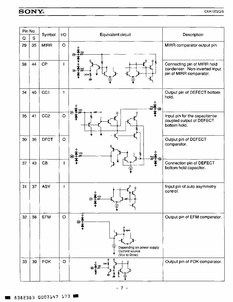
Pin No. Symbol 1/0 Equivalent circuit Description
a s 29 35 MIRA 0 MIRA comparator output pin.
...... ~ t,50 ~"!'
t h' • 38 44 CP I 1 I Connecting pin of MIRA hold
I I ........
®~ \~9 y !1 condenser. Non-inverted input
t 20K pin of MIRA comparator . • '-< ur 4
34 40 CC1 I Output pin of DEFECT bottom hold.
~ ~~~0 1~ ~=
I®- • -'AJ ... ~ ~"ee
35 41 CC2 0 ~ ,..
Input pin for the capacitance coupled output of DEFECT
I I ~ bottom hold. :
+ + _r t'~
30 36 DFCT 0 "i Output pin of DEFECT
~ comparator.
~~ 180 159~ ~
'= ~~ £>.
37 43 CB I ~~ =
Connection pin of DEFECT ..
~ bottom hold capacitor.
31 37 ASY I 1
L~ Input pin of auto asymmetry control.
3 • ,..180
~ ~ +
32 38 EFM 0 Output pin of EFM comparator. """ ~ =
'I" ~ E4.SK
• Depending on power supply Current source (Vee to DGND)
33 39 FOK 0 'l I 1 Output pin of FOK comparator. = 1811
~~{ff = ~
- 7 -
.. &3&23&3 0007147 173 ..

SON~
Pin No. Symbol 1/0
Q s 39 45 RFI I
40 46 RFO 0
42 48 TZC I
43 1 TE
44 2 TDFCT
45 3 ATSC
46 4 FZC
47 5 FE
48 6 FDFCT
Equivalent circuit
fir 40K
"""j~ 180
w.~ ~
. ~1.~?
@_ ~
180 4
75K
I Vee
~
180 46~-+---w,r-J
t "' ""'
'"
-~
t 7•A
56K
1.21<
- 8 -
.. 8382383 0007148 DOT ..
y
CXA13720/S
Description
Input pin with coupling capacitor where RF summing amplifier output is connected.
Output pin of RF summing amplifier and check point of eye pattern.
Input pin of tracking zero-cross comparator.
Input pin of tracking error amplifier.
Capacitor connecting pin for time constant during defects.
Window comparator input pin for ATSC detection.
Pin for focus zero-cross comparator input.
Input pin of focus error.
Capacitor connecting pin for time constant during defect functions.

I 0:0 w 0:0 rtl w 0:0 w
Cl Cl Cl -...1 1:-' -1= ..D
-3 -1= IT'
I
<0
Electrical Characteristics
No. Item
1 Current consumption
2 Current consumption
3 DC voltage gain
-
4 Field through
r-- F 5 0 Max. output voltage
1- c 6 u Max. output voltage
r-- s 7 s Max. output voltage
r-- E 8 R Max. output voltage
r-- v 9 0 Search output voltage
r--10 Search output voltage
r--
11 FZC threshold
12 DC voltage gain ,_
13 Field through
- T 14 R Max. output voltage
- A 15 c Max. output voltage K - I 16 N Max. output voltage
- G 17 Max. output voltage
- s 18 E Jump output voltage
- R 19 v Jump output voltage 0 -20 ATSC threshold
-21 ATSC threshold
-
22 TZC threshold
SW condition Symbol SD
S1 S2 S3 S4 S5 S6 S7 sa S9
Icc 00
lEE 00
GFEO 08
VFEOF 00
VFE01 0 08
VFE02 0 08
VFE03 0 0 08
VFE04 0 0 08
VSRCH1 02
VSRCH2 03
VFZC 00
GTEO 25
VTEOF 00
VTE01 0 25
VTE02 0 25
VTE03 0 0 25
VTE04 0 0 25
VJUMP1 2C
VJUMP2 28
VATSC1 20
VATSC2 20
Vrzc 20
Bias condition Test
E1 E2 E3 E4 point
10,36
19,41
5
5
5
5
5
5
5
5
* 27
11
11
11
11
11
11
11
11
* 27
27
* 27
Ta=25°C, Vcc=+2.5V, VEE-2.5V, D.GND=-2.5V
Output wafeform and description of test method
Min. Typ. Max. Unit
8 19 27 rnA
-8 -16 -22 mA
V1=10HZ, 100mVp-p 18.0 21.0 24.0 dB GFeo~20 log (Vout!Vin)
SG=10kHZ, 40mVp-p Difference in gain when -35 dB SD=OO and 80=08
V1=0.5Voc 2.0 v
V1=-0.5Voc -2.0 v
V1=0.5Voc 1.2 v
V1=-0.5Voc -1.2 v
-640 -360 mV
360 640 mV
*(Vcc+OGND)/2=SENS 39 50 61 mV value when E4 is varied.
V2~1 OHz, 500mVp-p 11.6 14.6 17.6 dB GrEo=20 log (VouWin)
V2=10kHz, 40mVp-p Difference in gain when -39 dB SD=OO and 80=25
V2~-0.SVoc 2.0 v
V2=0.5Voc -2.0 v
V2=-0.5Voc 1.2 v
V2=0.5Voc -1.2 v
-640 -360 mV
360 640 mV
*(Vcc+DGND)/2=SENS -45 -26 -7 mV
value when E3 is varied. 7 26 -45 mV
*(Vcc+DGND)/2 SENS -20 0 20 mV value when E2 is varied.
r.n 0 z ~
~ w """" 1\)
~

I (J:I
lJJ (J:I
ru w [):1
w
Cl Cl Cl --.I
""" t.n Cl
"\.I tr (J:I
I
.... 0
No.
23 1-
24
1--25
1--26
1--
27 1--
28 1--
29 1--
30 -
31
-32
-33
34
-35
-36
-37
38 -
39 ,____ 40
,____
41
1--
42
Item
DC voltage gain
Field through
s L Max. output voltage E D Max. output voltage
s Max. output voltage E R Max. output voltage v 0
Kick output voltage
Kick output voltage
SSTOP threshold
8EN8 low level
COUT low level
FOK threshold
F High level voltage
0 K Low level voltage
Max. operating frequency
High level voltage
Low level voltage
M I Max. operating frequency R R Min. input operating 0 volatage R
Max. input operating voltage
SW condition Bias condition Symbol SD
S1 S2 S3 S4 S5 S6 57 88 89 E1 E2 E3 E4
GsLO 25
VF:Jli' 00
Va01 25
VarJ?. 25
Vam 0 25
Va01 0 25
VKICK1 22
VKICK2 23
VSi:rra> 30 * Vsa-s
VOOJT
VFO\f
VFO<H
VFO'J..
FFOK
VMIRH
VMIRL
FMIR
VMIR1
VMIR2
Test Output wafeform and point description of test method Min.
14 Vs:10Hz, 20mVp-p
50 Open loop gain
Vs=1 OkHz, 1 OOmVp-p 14 Difference in gain when
SD=OO and SD=25
14 Vs=1.0Voc 2.0
14 Vs=-1.0Voc
14 Vs=1.0Voc 2.0
14 Vs=-1.0Voc
14 -750
14 450
27 *(Vcc+DGND)f2=SENS
-40 value when E1 is varied.
27
26
(Vcc+DGND)/2 the voltage 33 between Pins 39 and 40 --400
when V4 is varied.
33 2.2
33 V4=1Vp-p- 375m\bc
33 45
29 V4=10kHz
1.8
29 1.0Vp-p- 0.4Voc
29 V4=800mVp-p - 0.4Voc 30
29
V4=10kHz,- 0.4Voc
29 1.8
Typ. Max.
-34
-2.0
-2.0
-450
750
-25 -10
-2.0
-2.0
-356 -330
-1.8
-2.0
0.3
Unit
dB
dB
v
v
v
v
mV
mV
mV
v
v
mV
v
v
kHz
v
v
kHz
Vp-p
Vp-p
f/l 0 z t<
(')
~ (..) --.1 r>,)
~

I (J:I
lJJ ():1
ru lJJ ():1
lJJ
Cl Cl Cl -..I I:-' (.n
I:-'
cr -I ..t:"
I
No.
43 -
44 -
45 1--
46 1--
47
1--
48
1--49
50 -
51 -
52 -
53
-54
Item
High level output voltage
Low level output voltage
Min. operating frequency
D E Max. operating frequency
F E Min. input operating c voltage T
Max. 1nput operating voltage
Duty 1
Duty 2
High level output voltage
E Low level output voltage F M Min. input operating
voltage
Max. input operating voltage
SW condition Symbol
S1 S2 S3 S4 ss S6 S7 sa
VDFCTH
VDFCTL
FDFCT1
FDFCT2
VDFCT1
VDFCT2
OmA1 0
DEFM2 0
VEFMH 0
VEFML 0
VEFM1 0
VEFM2 0
Bias condition Test Output wafeform and SD po1nt description of test method
Min. S9 E1 E2 E3 E4
30 1.8
30
30 V4=40mVp-p + t 5mVoc
30 2.5
30
V4=50Hz + 15mVoc
30 1.8
31 V4=750kHz, 0.7Vp-p -50
31 V4=750kHz,
0 0.7Vp-p + 0.25Voc
0 32 1.2 V4=750kHz, 0.7Vp-p
0 32
A V4=750kHz
A 1.8
Typ. Max.
-2.0
t
0.5
0 50
50 100
-1.2
0.12
Umt
v
v
kHz
kHz
Vp-p
Vp-p
mV
mV
v
v
Vp-p
Vp-p
rn 0 z ~
0
~ w g en

Electric Characteristics Test Circuit
"' "' > 0
GND
.. 8382383 0007152 530 ..
CXA1372Q/S
GND GND GND
- 12 -

SON~ CXA13720/S
Description of Functions
Focus servo system
1.2K
Above is a block diagram of the focus servo system. FE signal is gradually input to focus phase compensation circuit through 20k.Q and 48k.Q resistances.
However, when DFCT is detected, FE signal is switched into the low pass filter route formed by connecting a capacitance between the built-in 470kn resistance and Pin 48.
When this DFCT counter measure circuit is not used, Pin 48 is left open. When FS3 is on, the high frequency gain can be reduced by forming a low frequency time constant through a
capacitor connected across Pins 2 and 3 and the internal resistor. The capacitor across Pin 4 and GND is a time constant that raises low frequency normally in playback
condition. The peak frequency of the focus phase compensation is inversely proportional to the resistor connected to Pin 16 (about 1.2kHz when the resistor is 51 Ok.O).
The focus search peak becomes about ±1.1 Vp-p with the above constant. The peak is inversely proportional to the resistor connected across Pin 17 and GND. However, when this resistor is varied, the peaks of track jump and sled kick also vary.
FZC comparator inverted input is set to 2% of the difference between the reference voltage Vee and VC (Pin 1): (Vee- VC) x 2%.
Note: For Pin 16 a 51 Ok.Q resistor is recommended.
- 13 -
.. 8382383 0007153 477 ..

SONY®
Tracking sled servo system
470K
TZC
Trackmg phase compensation
FSET
Above is a block diagram of the tracking and sled servo system.
CXA1372Q/S
The capacitor across Pins 8 and 9 has a time constant to reduce high frequency when TG2 is switched off. The tracking phase compensation peak frequency is at about 1.2kHz when the resistor connected to Pin 16 is at 510kQ.
For a tracking jump in FWD or REV direction, TM3 or TM4 is set on. At this time, the peak voltage fed to the tracking coil is determined by the TM3 and TM4 current values and the feedback resistor from Pin 12. That is:
Track jump peak voltage = TM3 (TM4) current value x feedback resistor value. The FWD or REV sled kick is done by setting TM5 or TM6 on. At this time, the peak voltage added to the sled motor is determined by the TM5 or TM6 current value and the feedback resistor from Pin 15.
Sled jump peak voltage = TM5 (TM6) current value x feedback resistor value. Each SW current value is determined by the resistor connected to Pin 17 and GND when the resistor is at about 120kU.
TM3 or TM4 turns to ±11 JlA and TM5 or TM6 to ±22Jl.A. This current value is almost inversely proportional to the resistor, variable within a range of about 5 to 401J.A
forTM3. S STOP is the ON/OFF detection signal for the limit SW of the linear motor's innermost circumference. TE signal is switched into low pass filter route formed by connecting a capacitance between the built-in
resistance at DFCT (470kU) and Pin 44 as for FE signal. TM1 was ON at DFCT in CXA 1082 and CXA 1182, but it is not operational in CXA 1372.
- 14 -
.. 8382383 0007154 303 ..

SON~
Focus OK circuit
I From RF summing amplifier I I I
l!5K 92K
0.62!5V I FOCUS OK AMP
Vee
20K
FOCUS OK
Focus OK circuit generates a timing window to enable focus servo from a focus search condition.
CXA1372Q/S
RF signal from Pin 46 is passed through HPF (High Pass Filter) and output from Pin 39. RF signal passed through LPF (Low Pass Filter) is output from Pin 33.
Focus OK amplifier output is inverted when VRFI-VRFo#-Q.37V. C5 determines the time constants of HPF in the EFM comparator and mirror circuits as well as that of LPF in
the focus OK amplifier. Normally, when 0.01 J..lF is selected for CS, fc (cut-off frequency} = 1kHz. This prevents the block error rate from worsening as the result of a damaged RF envelope due to scratched disc, etc.
- 15 -
.. 8382383 0007155 24T ..

SONY® CXA1372Q/S
EFM comparator EFM comparator changes RF signal a binary value. The asymmetry generated due to variations in disc
manufacturing cannot be eliminated by the AC coupling alone. Therefore, the reference voltage of EFM comparator is controlled through 1 and 0 that are in approximately equal numbers in the binary EFM signals. vc
I r----
RFI
A~~:T~M~;;Rv I
I I I I I I I I I
OGNO=OV
' ~------------------~32:r-----------~.~~ EFM
I I EFM COMPARATOR I L-------------------------~
I L----CXD2500
As this comparator is a current SW type, each of the Hand L levels is not equal to the power supply voltage. A feedback has to be composed through the CMOS buffer.
R8, R9, C8, and C9 form a LPF to obtain (Vee+ DGND)/2V. When fc (cut-off frequency) exceeds 500Hz, EFM low-frequency components leak badly, and the block error rate worsens.
DEFECT circuit After inversion, RFI signal is bottom held by means of one long and one short time constant. The short time
constant bottom hold responds to a disc mirror defect inexcess of 0.1 msec. The long time-constant bottom hold keeps to the mirror level prior to the defect. By differentiating this with a
capacitor coupling and shifting the level, both signals are compared to generate a mirror defect detection signal.
0.033)1
r----------
1 1
DEFECT COMPARATOR
DEFECT AMP
o RFO
b DEFECT AMP
e OEFECT
.. 8382383 0007156 186 ..
mAIIIrtNrllliiW&-~ -·~· · 00111~ II
__Il _ ______.
- 16 -
H
L
BOTTOM HOLDI2)
Dotted fine CC2
SONY® CXA1372Q/S
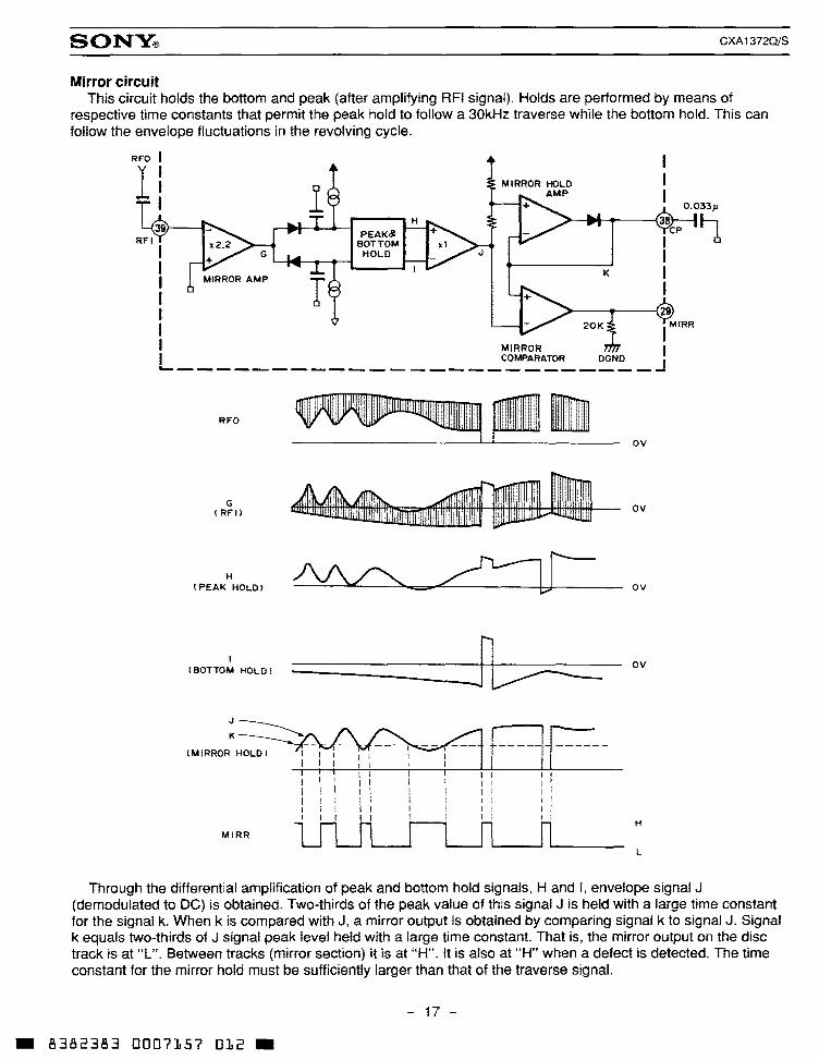
Mirror circuit This circuit holds the bottom and peak (after amplifying RFI signal). Holds are performed by means of
respective time constants that permit the peak hold to follow a 30kHz traverse while the bottom hold. This can follow the envelope fluctuations in the revolving cycle.
RFO
RFI
I I I I I I I MIRR
I MIRROR I I COMPARATOR DGND
--------------------------~
RFO
G !Rf"ll
H !PEAK HOLDl
I
I BOTTOM HOLD l n
-----J~
'"'"oo"~~f----lE-' I I \ : I 1 \ : : :
I I I I I I I 1 I 1 I I I I I I I I 1 I I I I i I I I I I I I I I I I I I I I I I I II
MIRR
ov
ov
ov
H
L
Through the differential amplification of peak and bottom hold signals, Hand I, envelope signal J (demodulated to DC) is obtained. Two-thirds of the peak value of this signal J is held with a large time constant for the signal k. When k is compared with J, a mirror output is obtained by comparing signal k to signal J. Signal k equals two-thirds of J signal peak level held with a large time constant. That is, the mirror output on the disc track is at "L". Between tracks (mirror section) it is at "H". It is also at "H" when a defect is detected. The time constant for the mirror hold must be sufficiently larger than that of the traverse signal.
- 17 -
.. 8382383 0007157 012 ..
CXA13720/S
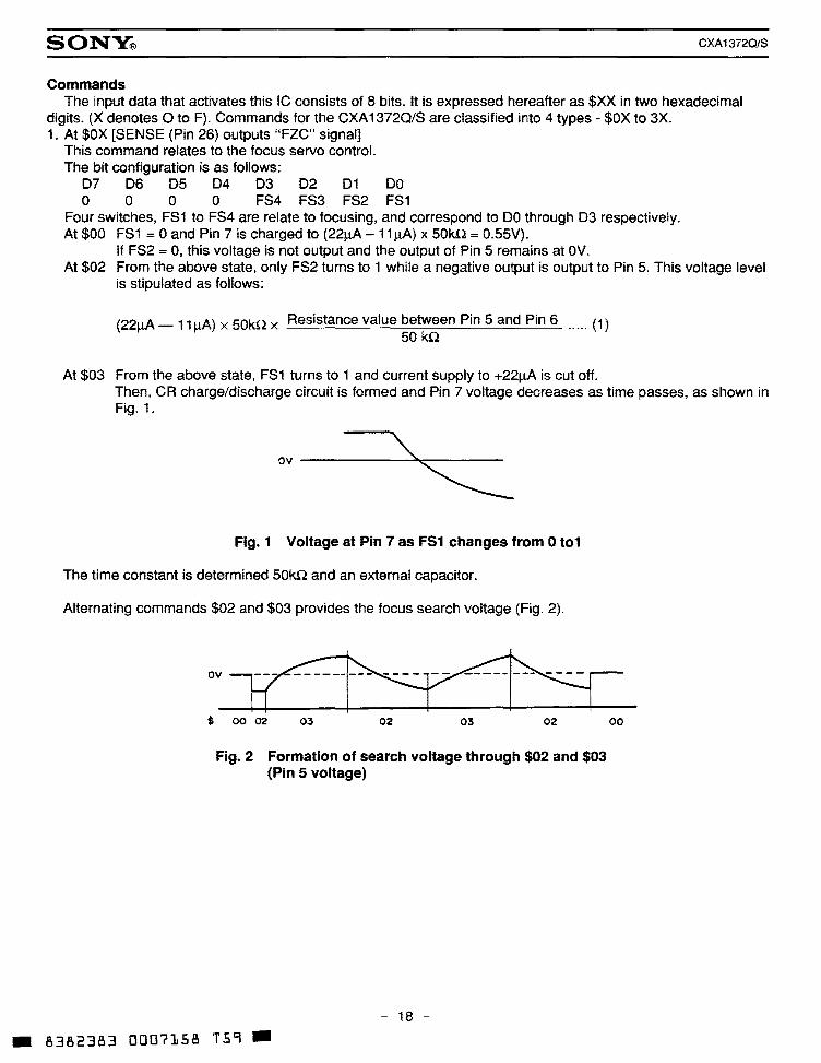
Commands The input data that activates this IC consists of 8 bits. It is expressed hereafter as $XX in two hexadecimal
digits. (X denotes 0 to F). Commands for the CXA 13720/S are classified into 4 types - $OX to 3X. 1. At $OX [SENSE (Pin 26) outputs "FZC" signal]
This command relates to the focus servo control. The bit configuration is as follows:
07 06 05 04 03 02 01 DO 0 0 0 0 FS4 FS3 FS2 FS1
Four switches, FS1 to FS4 are relate to focusing, and correspond to DO through D3 respectively. At $00 FS1 = 0 and Pin 7 is charged to (22J.1A- 11J.1A) x 50kn = 0.55V).
If FS2 = 0, this voltage is not output and the output of Pin 5 remains at OV. At $02 From the above state, only FS2 turns to 1 while a negative output is output to Pin 5. This voltage level
is stipulated as follows:
(22JlA _ 11 JlA) x 50kn x Resistance value between Pin 5 and Pin 6 ..... (1) 50kn
At $03 From the above state, FS1 turns to 1 and current supply to +22J.1A is cut off. Then, CR charge/discharge circuit is formed and Pin 7 voltage decreases as time passes, as shown in Fig. 1.
ov ------""'~..,...------~ Fig. 1 Voltage at Pin 7 as FS1 changes from 0 to1
The time constant is determined 50kn and an external capacitor.
Alternating commands $02 and $03 provides the focus search voltage (Fig. 2).
ov~ $ 00 02 03 02 03 02
Fig. 2 Formation of search voltage through $02 and $03 (Pin 5 voltage)
- 18 -
.. 8382383 0007158 T59 ..
00

CXA1372Q/S
1) FS4 description This switch is placed between focus error input 47 and the focus phase compensation to switch the
focus servo on and off. $00 ~ $08
Focus off f- Focus on
2) Focus application For explanation sake the polarity is assumed as follows: a)The lens moves away or toward the disc in search. b)At this time, output voltage at Pin 5 varies from negative to positive. c)Further on, the focus S-curve changes as follows:
Fig. 3 S-curve
Focus servo is activated at operating point A shown in Fig. 3. Usually, focus search is performed and focus servo switch set ON when passing through A point in Fig. 3. Moreover, to prevent misoperation, a logical product (AND) is timed with the Focus-OK signal.
This IC is designed to output FZC (Focus Zero Cross) from Sense Pin (Pin 26), as the A point passing signal. Focus-OK signal is output to indicate focus in ON (focus is enabled in this case). The following time chart
shows how to obtain the focus.
Drive voltage
Focus error
Sense pin (FZC)
Focus OK
C 20 ms IC 200ms I
$02 I I "I I
1$00 I 1.._ I I'~ I
I I I I
$03
I I
$08
---
-------------~---,--~--~------1\ ," I ,_,
I I I
t_ The moment focus is ON.
I I I
L-------------
Fig. 4 Timing Chart of In-Focus
- 19 -
.. 8382383 0007159 995 ..
Dotted lines in the diagram after a case where a focus cannot be applied.

CXA1372Q/S
It is important here that $08 command be transferred in the shortest possible time after FZC changes from H to L. To this effect, (b) sequence required for software is favoured over (a) sequence, shown below.
(a) (b)
Fig. 5 Bad Sequence and Good Sequence Better case (at right) recommended over poor sequence (at left)
3) Sense Pin (Pin 27) Output at Sense Pin varies according to the input data. That is: FZC is output with $OX.
AS is output with $1 X. TZC is output with $2X. SSTOP is output with $3X. HIGH-Z is output with $4X to 7X.
2. At $1 X SENS (Pin 27 outputs signal "AS") This command refers to ON/OFF of TG1, TG2 and the brake circuit. The bit configuration is as follows:
07 06 05 0 0 0
TG1, TG2
04 03 02 01 DO 1 ANTI Brake TG2 TG 1
SHOCK Circuit ON/OFF ON/OFF
These switches sele~t Up/Normal of the tracking servo gain. The brake circuit prevents the erratic motion of the actuator. After 1 00-track or 1 0-track jumps, the servo circuit exceeds the linear range and the actuator often sets on the wrong track. Using a feature where the RF envelope and the tracking error are out of phase by 180° braking is applied when the actuator crosses the tracks either way to cut off tracking errors and stop undesirable jumping.
- 20 -
.. 8382383 00071b0 b07 ..
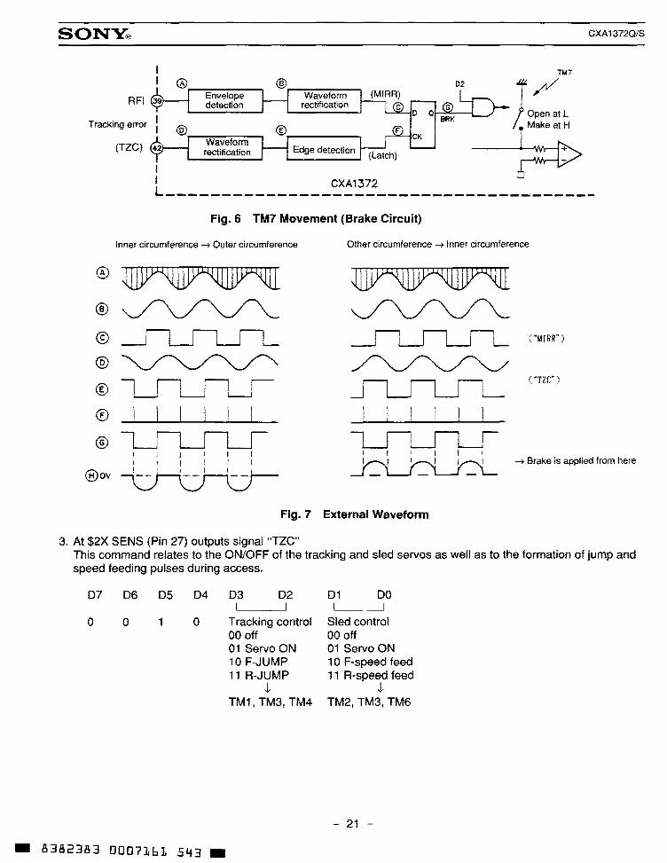
SONY® CXA1372Q/S
® RFI Envelope Waveform
detection rectification
Tracking error I I ®
(TZC} Waveform rectification Edge detection
I I CXA1372 L---------------------------------------
Fig. 6 TM7 Movement (Brake Circuit)
Inner circumference ---7 Outer circumference Other circumference ---? Inner circumference
®
@
@
®~.__j" ® I I I I I I ®
@ov
Fig. 7 External Waveform
3. At $2X SENS (Pin 27) outputs signal "TZC"
C "MI RR")
("TZC")
---? Brake is applied from here
This command relates to the ON/OFF of the tracking and sled servos as well as to the formation of jump and speed feeding pulses during access.
07 06 05 04 03 02 01 DO
0 0 0 Tracking control Sled control 00 off 00 off 01 Servo ON 01 Servo ON 10 F-JUMP 1 o F-speed feed 11 R-JUMP 11 R-speed feed
J.. J.. TM1, TM3, TM4 TM2, TM3, TM6
- 21 -
.. 8382383 0007161 543 ..

SONY® CXA1372Q/S
DIRC (Pin 20) and 1 Track Jump Normally, an acceleration pulse is applied for a 1-track jump. Then a deceleration pulse is given for a specified time observing the tracking error from the moment it passes point 0 tracking servo is set on again after applying a deceleration pulse for a specified time. For the 1 00-track jump to be explained in the next item, as long as the number of tracks is about 1 00 there is no problem. However for the 1-track jump it must be exactly a 1-track jump, which requires the above complicated procedure. For the 1-track jump in CD players, both the acceleration and deceleration take about 300 to 400!!S. When software is used to execute this operation, it turns out as shown in the flow chart of Fig. 9. Actually, it takes time to transfer data.
Pulse waveform
Tracking error
Fig. 8 Pulse Waveform and Tracking Error of 1-Track Jump
{TR: REV SL: OFF
{ TR: FWD SL:OFF
Execute
{TR:ON SL:ON
Execute
Execute
{ TR: REV SL: OFF
{TR: FWD
SL: OFF
{ TR: ON SL:ON
Execute
We have:
We have:
Fig. 9 1-Track Jump not using DIRC 20 Fig. 10 1-Track Jump with DIRC 20
"DIRC" (Direct Control) Pin was provided in this IC to facilitate the 1-track jumping operation. That is to perform for1-track jump using DIRC, the following process takes place (DIRC =normal H). (a) Acceleration pulse is output. ($2C for REV or $28 for FWD). (b) With TZC ,J.. (or TZC i), set DIRC to L. (SENS Pin 27 outputs "TZC"). As the jump pulse polarity is
inverted, deceleration is applied. (c) Set DIRC to H for a specific time.
Both the tracking servo and sied servo are switched on automatically. As a result, the track jump turns out as shown in the flow chart of Fig. 10 and the two serial data transfers can be omitted.
- 22 -
.. 8382383 0007162 48T ..

CXA1372Q/S
4. $3X This command selects the Focus search and Sled kick peak values.
DO, D1 ..... Sled, NORMAL feed, high-speed feed D2, D3 ..... Focus search peak selection
Focus search peak Sled kick peak
D3 D2 D1 DO Relative D7 D6 D5 D4
(PS1) value (PS3) (PS2) (PSO)
0 0 0 0 ±1
0 0 1 1 0 1 0 1 ±2
1 0 1 0 ±3
1 1 1 i ±4
- 23 -
.. 8382383 0007163 316 ..

SONY®
Parallel Direct Interface
1. DIRC
$ 281atch
ll I
XLT u I
t DIRC I t I I I I
FWD JUMP ON' I I OFF I
I I I
REV JUMP I ONI
I
OFF I I I
ON OFF'
I TRACKING SERVO I
I
I I
ON OFF I I SLED SERVO
f
I I I I I I I I I I
I
2. LOCK (Sled runaway prevention circuit)
LOCK
ON OFFI~.. _____ ...,j SLED SERVO
----------------~' OFF ~~-----....J
I
ON TG1,TG2
TRACKING GAIN OOWN
- 24 -
.. 8382383 0007164 252 ..
$2C latch
J.l I u I
I l I
1!----___,] i I
CXA13720/S

SON~
CPU Serial Interface Timing Chart
DATA DO 02x03~05x06x07 I su j _j ~...---.!!-
CLK
XLT
DVcc- DGND = 4.5 to 5.5V
Item Symbol Min. Typ. Max. Unit
Clock frequency fck 1 MHz
Clock pulse width fwck 500 ns
Setup time tsu 500 ns
Hold time th 500 ns
Delay time tD 500 ns
Latch pulse width twL 1000 ns
System Control
ADDRESS DATA Item
D7 D6 D5 D4 D3 D2 D1 DO
FS4 FS3 FS2 FS1 Focus Control 0 0 0 0 Focus Gain Search Search
ON Down ON UP
Tracking Control 0 0 0 1 Anti Brake TG2 TG1 Shock ON Gain Set *1
Tracking Mode 0 0 1 0 Tracking Mode *2 Sled Mode *3
PS4 PS3 PS2 PS1 Select 0 0 1 1 Focus Focus Sled Sled
Search+2 Search+1 Kick+2 Kick+1
Note) *1. GAIN SET TG1 and TG2 can be set independently. When the anti-shock is at 1 (00011 xxx), invert both TG1 and TG2 when the internal antishock is at H.
*2. TRACKING MODE *3. SLED MODE
D3 D2 D1 DO
OFF 0 0 OFF 0 0
ON 0 1 ON 0 1
FWD JUMP 1 0 FWD MOVE 1 0
REV JUMP 1 1 REV MOVE 1 1
- 25 -
.. 8382383 0007165 199 ..
CXA1372Q/S
SENS Output
FZC
A.S
TZC
SSTOP

SONY® CXA1372Q/S
Serial Data Truth Table
Serial data Hexa. Function
FOCUS CONTROL FS = 4321
00000000 $00 0000 00000001 $01 0001 00000010 $02 0010 00000011 $03 0011 00000100 $04 0100 00000101 $05 0101 00000110 $06 0110 00000111 $07 0111 00001000 $08 1000 00001001 $09 1001 00001010 $0A 1010 00001011 $08 1011 00001100 $0C 1100 00001101 $00 1101 00001110 $0E 1110 00001111 $OF 1111
AS=O AS=1 TRACKING CONTROL
TG=2 1 TG=2 1 00010000 $10 0 0 0 0 00010001 $11 0 1 0 1 00010010 $12 1 0 1 0 00010011 $13 1 1 1 1 00010100 $14 0 0 0 0 00010101 $15 0 1 0 1 00010110 $16 1 0 1 0 00010111 $17 1 1 1 1 00011000 $18 0 0 1 1 00011001 $19 0 1 1 0 00011010 $1A 0 1 0 1 00011011 $18 1 1 0 0 00011100 $1C 0. 0 1 1 00011101 $10 0 1 1 0 00011110 $1E 1 0 0 1 00011111 $1F 1 1 0 0
- 26 -
.. 8382383 0007166 025 ..

CXA1372Q/S
TRACKING MODE DIRC=1 DIRC=O DIRC=1
™=654321 654321 654321
00100000 $20 000000 001000 000011 00100001 $21 000010 101010 000011 00100010 $22 010000 011000 100001 00100011 $23 100000 101000 100001 00100100 $24 000001 000100 000011 00100101 $25 000011 000110 000011 00100110 $26 010001 010100 100001 00100111 $27 100001 100100 100001 00101000 $28 000100 001000 000011 00101001 $29 000110 001010 000011 00101010 $2A 010100 011000 100001 00101011 $28 100100 101000 100001 00101100 $2C 001000 000100 000011 00101101 $2D 001010 000110 000011 00101110 $2E 011000 010100 100001 00101111 $2F 101000 100100 100001
- 27 -
.. 8382383 0007167 T61 ..

CXA13720/S
Others
1 . Connection of the power supply pin
Vee VEE vc ±5V dual power supply +5V -5V ov 5V single power supply +5V ov vc
2. FSET pin
FSET pin determines the high frequency phase compensation for Focus and Tracking servo, and the cut-off frequency (fc) of CLV LPF.
3. ISETpin
ISET current = 1.27V/R = Focus search current ($30) =Tracking kick current = 1/2 sled kick current ($30)
4. In the tracking amplifier, input is clamped at 1 VsE to prevent over input.
5. How to change FE and TE gains
(1) To increase: Pins® and®. Pins@ and @to more than 1 OOkn
(2) To decrease: Divide FE and TE input resistance
6. Microcomputer interface 20 to 25, set input voltage of pin to
more than V1HVcc x 90% less than V1L Vee x 1 0%
7. Focus OK circuit
(1) To set the time constants for the focus OK amplifier LPF and the mirror amplifier HPF refer to the paragraph on Description of Operations.
- 28 -
.. 8382383 0007168 9T8 ..

SONY®
(2) The equivalent circuit of FOK output pin is as follows,
OGND OGND
Accordingly FOK comparator output is: Output voltage H: VFOKH =near Vee Output voltage L: VFOKL = Vsat (NPNl + DGND
8. Mirror Circuit
(1) The equivalent circuit of MIRA output pin is as follows.
VI!:E OGND
MIRA comparator output is: Output voltage H: VMIRH =Vee- Vsat(LPNP) Output voltage L: VMIRL =near DGND
9. EFM Comparator
Vee
DGND
(1) Note that EFM duty varies when CXA 1372 Vee differs from that of DSP IC (Such as CXD2500).
(2) The equivalent circuit of EFM output pin is as follows.
CXA1372Q/S
*The power supply current is given as SV from Vee to DGND. Then we have EFM comparator output as follows,
Output voltage H: VEFMH =Vee- VBE (NPNJ Output voltage L: VEFML = Vee- 4.8 (kQ) x 7 (}.!A) - VBE (NPN)
- 29 -
.. 8382383 0007169 834 ..

I Q:J
w Q:J
ru w Q:J
w
CJ CJ c::J "\.1 1:-' "\.1 c::J
(.n (.n
IT'
I
(..) 0
Focus Tracking Internal Phase Compensation Standard Circuit Design Data
SW condition Bias condition MODE Item Symbol so
Sl S2 S3 S4 S5 S6 S7 sa S9 El E2 E3 E4
1.2kHz gain 0 F 0 1 .2kHz phase 0 c u 1.2kHz gain 0 s
1 .2kHz phase 0
T 1.2kHz gain 0 R A 1.2kHz phase 0 c K
2.7kHz gain 0 I N G 2. 7kHz phase 0
Test Output waleform and point description of test method Min. Typ.
5 When CFLB=0.1!!F 21.5
5 63
5 16
5 63
11 13
11 -125
11 265
11 -130
Max. Unit
dB
deg
dB
deg
dB
deg
dB
deg i
ttl 0 z ~
(')
~ w
§

SONY®
Tracking frequency characteristics
-- ' ... ',1 / G 1'
/ // r------.- '
""' ' \
I / \
Vi/ ~ \ \
r--- _-:---=;; ' 1\ \ ~
~ --- ' \ - "":::> ~ v \!\: \ \ ----- \
\
- - NORMAL I \' ' -
-- - GAIN UP ' \ ' CTGU = 0.033J.!
I I I .\'\ ... \~ .•. f - Frequency (Hz)
FOCUS frequency characteristics
! I CFLB = 0.1Jl
-
~
. .•.
---
.. 8382383 0007171 492 ..
_CFDG = 0.1Jl
£ / /
~ / ~(~ --' ' --- ---
.•.
/ -=-::::.. ' ~ / Zi - -
'\(./ G _L/ ' "/ /
/! // /
\ /
/ ,1 4J \, J / / I
/ ;
~. ,' "\ /
/
/ :/ r- NORMAL J -
/ /
-GAIN UP / --/
I I ••'
f - Frequency (Hz)
- 31 -
" ',0
1\
"" \
'\ '
~ 00 . ..
CXA1372Q/S

SONY®
Package Outline Unit: mm
CXA1372Q
37
48
CXA1372S
48
~ 0
.. 8382383 0007172 329 ..
48pin QFP (Plastic)
0 1 5.3 ±0.4
012.0 ~ 8:1
36 25
+ 0.15 --+---1-"'0'"'-8 0.3-0,1
24
13
± 0.12 @ +0.3 22-0;1
48pin SDIP (Plastic)
t 0.4 4 3.2-0.1
'"'"' mn
- 32 -
25
Jo
=r~d ~ +' LO rt> cl <:i
= ~ 0 M
0.6g
• 0.1 0.1 5 -0,05
QFP-48P-L04
600mil5.1g
SDIP-48P-02
CXA1372Q/S
43371