RF power transistor the LdmoST plastic family - Home - … · December 2007 Rev 1 1/16 16 PD84002...
16
December 2007 Rev 1 1/16 16 PD84002 RF power transistor The LdmoST plastic family Features ■ Excellent thermal stability ■ Common source configuration ■ Broadband performances P OUT = 2 W with 13 dB gain @ 870 MHz ■ Plastic package ■ ESD protection ■ Supplied in tape and reel ■ In compliance with the 2002/95/EC european directive Description The PD84002 is a common source N-channel, enhancement-mode lateral Field-Effect RF power transistor. It is designed for high gain, broad band commercial and industrial applications. It operates at 7 V in common source mode at frequencies of up to 1 GHz. PD84002’s superior gain and efficiency makes it an ideal solution for portable radio and UHF RFID reader. Figure 1. Pin connection SOT-89 Source Gate Source Drain Figure 2. Device summary Order code Marking Package Packaging PD84002 8402 SOT-89 Tape and reel www.st.com
Transcript of RF power transistor the LdmoST plastic family - Home - … · December 2007 Rev 1 1/16 16 PD84002...

December 2007 Rev 1 1/16
16
PD84002RF power transistor
The LdmoST plastic family
Features Excellent thermal stability
Common source configuration
Broadband performances POUT = 2 W with 13 dB gain @ 870 MHz
Plastic package
ESD protection
Supplied in tape and reel
In compliance with the 2002/95/EC european directive
DescriptionThe PD84002 is a common source N-channel, enhancement-mode lateral Field-Effect RF power transistor. It is designed for high gain, broad band commercial and industrial applications. It operates at 7 V in common source mode at frequencies of up to 1 GHz.
PD84002’s superior gain and efficiency makes it an ideal solution for portable radio and UHF RFID reader.
Figure 1. Pin connection
SOT-89
Source
GateSource
Drain
Figure 2. Device summary
Order code Marking Package Packaging
PD84002 8402 SOT-89 Tape and reel
www.st.com
Contents PD84002
2/16
Contents
1 Electrical data . . . . . . . . . . . . . . . . . . . . . . . . . . . . . . . . . . . . . . . . . . . . . . 3
1.1 Maximum ratings . . . . . . . . . . . . . . . . . . . . . . . . . . . . . . . . . . . . . . . . . . . . 3
1.2 Thermal data . . . . . . . . . . . . . . . . . . . . . . . . . . . . . . . . . . . . . . . . . . . . . . . 3
2 Electrical characteristics . . . . . . . . . . . . . . . . . . . . . . . . . . . . . . . . . . . . . 4
2.1 Static . . . . . . . . . . . . . . . . . . . . . . . . . . . . . . . . . . . . . . . . . . . . . . . . . . . . . 4
2.2 Dynamic . . . . . . . . . . . . . . . . . . . . . . . . . . . . . . . . . . . . . . . . . . . . . . . . . . . 4
2.3 ESD protection characteristics . . . . . . . . . . . . . . . . . . . . . . . . . . . . . . . . . . 4
2.4 Moisture sensitivity level . . . . . . . . . . . . . . . . . . . . . . . . . . . . . . . . . . . . . . . 4
3 Impedances . . . . . . . . . . . . . . . . . . . . . . . . . . . . . . . . . . . . . . . . . . . . . . . . 5
4 DC curves . . . . . . . . . . . . . . . . . . . . . . . . . . . . . . . . . . . . . . . . . . . . . . . . . 6
5 RF curves . . . . . . . . . . . . . . . . . . . . . . . . . . . . . . . . . . . . . . . . . . . . . . . . . . 7
6 Schematic and BOM . . . . . . . . . . . . . . . . . . . . . . . . . . . . . . . . . . . . . . . . . 8
7 Photo . . . . . . . . . . . . . . . . . . . . . . . . . . . . . . . . . . . . . . . . . . . . . . . . . . . . . 9
8 Package mechanical data . . . . . . . . . . . . . . . . . . . . . . . . . . . . . . . . . . . . 10
8.1 Thermal Pad and Via design . . . . . . . . . . . . . . . . . . . . . . . . . . . . . . . . . . 12
8.2 Soldering profile . . . . . . . . . . . . . . . . . . . . . . . . . . . . . . . . . . . . . . . . . . . . 13
9 Revision history . . . . . . . . . . . . . . . . . . . . . . . . . . . . . . . . . . . . . . . . . . . 15

PD84002 Electrical data
3/16
1 Electrical data
1.1 Maximum ratings
1.2 Thermal data
Table 1. Absolute maximum ratings (TCASE = 25°C)
Symbol Parameter Value Unit
V(BR)DSS Drain-source voltage 25 V
VGS Gate-source voltage -0.5 to +15 V
ID Drain current 2 A
PDISS Power dissipation 6 W
TJ Max. operating junction temperature 150 °C
TSTG Storage temperature -65 to +150 °C
Table 2. Thermal data
Symbol Parameter Value Unit
RthJC Junction - case thermal resistance 21 °C/W

Electrical characteristics PD84002
4/16
2 Electrical characteristics
TCASE = +25 oC
2.1 Static
2.2 Dynamic
2.3 ESD protection characteristics
2.4 Moisture sensitivity level
Table 3. Static
Symbol Test conditions Min Typ Max Unit
IDSS VGS = 0 V VDS = 25 V 1 µA
IGSS VGS = 5 V VDS = 0 V 1 µA
VGS(Q) VDS = 7.5 V ID = 100 mA 3.9 V
VDS(ON) VGS = 10 V ID = 0.25 A 0.27 V
CISS VGS = 0 V VDS = 7.5 V f = 1 MHz 16 pF
COSS VGS = 0 V VDS = 7.5 V f = 1 MHz 16 pF
CRSS VGS = 0 V VDS = 7.5 V f = 1 MHz 1.2 pF
Table 4. Dynamic
Symbol Test conditions Min Typ Max Unit
POUT VDD = 7.5 V, IDQ = 100 mA, PIN = 0.1 W, f = 870 MHz 2 W
GPS VDD = 7.5 V, IDQ = 100 mA, POUT = 2 W, f = 870 MHz 13 15 dB
ND VDD = 7.5 V, IDQ = 100 mA, POUT = 2 W, f = 870 MHz 60 65 %
Load
mismatch
VDD = 7.5 V, IDQ = 100 mA, POUT = 2 W, f = 870 MHz
All phase angles20:1 VSWR
Table 5. ESD protection characteristics
Test conditions Class
Human body model 2
Machine model M3
Table 6. Moisture sensitivity level
Test methodology Rating
J-STD-020B MSL 3

PD84002 Impedances
5/16
3 Impedances
Figure 3. Impedances
Table 7. Impedances
F(MHz) ZGS ZDL
860 1,80 + j 7,79 3,88 + j 2,41
870 1,84 + j 7,96 3,89 + j 2,69
880 1,83 + j 8,01 4,01+ j 2,96
890 1,76 + j 8,11 4,17 + j 3,16
900 1,70 + j 8,20 4,27 + j 3,32
910 1,63 + j 8,30 4,37 + j 3,40
920 1,57 + j 8,48 4,41 + j 3,46
930 1,43 + j 8,64 4,36 + j 3,51
940 1,41 + j 8,83 4,28 + j 3,51

DC curves PD84002
6/16
4 DC curves
Figure 4. DC output characteristics Figure 5. ID vs VGS
Figure 6. Capacitances vs drain voltage
VGS=10VVGS=9VVGS=8V
VGS=7V
VGS=6V
VGS=5V
VGS=4V
ID vs Vgs
PD84002
0
5
10
15
20
25
30
0 2 4 6 8 10 12 14 16
Vdd (V)
Cap
acita
nce
(pF)
CRSS COSS CISS
PD84002 RF curves
7/16
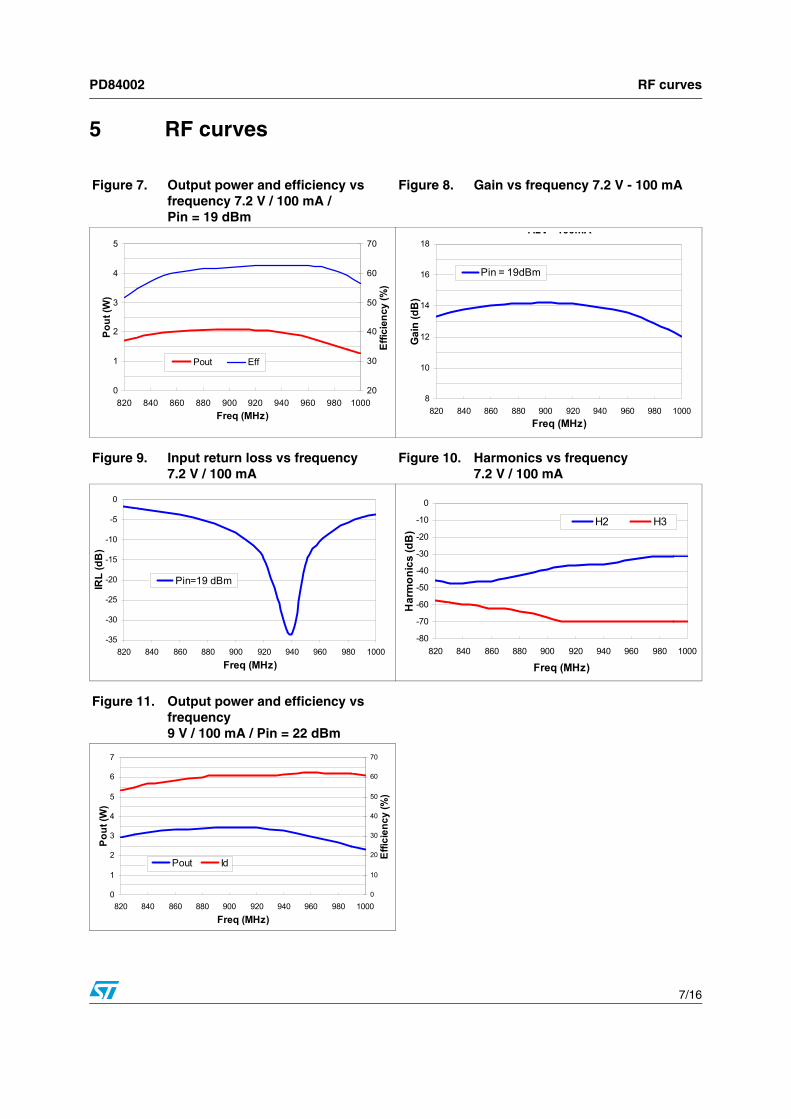
5 RF curves
Figure 7. Output power and efficiency vs frequency 7.2 V / 100 mA / Pin = 19 dBm
Figure 8. Gain vs frequency 7.2 V - 100 mA
Figure 9. Input return loss vs frequency 7.2 V / 100 mA
Figure 10. Harmonics vs frequency 7.2 V / 100 mA
Figure 11. Output power and efficiency vs frequency 9 V / 100 mA / Pin = 22 dBm
0
1
2
3
4
5
820 840 860 880 900 920 940 960 980 1000Freq (MHz)
Pout
(W)
20
30
40
50
60
70
Effic
ienc
y (%
)
Pout Eff
7.2V 100mA
8
10
12
14
16
18
820 840 860 880 900 920 940 960 980 1000Freq (MHz)
Gai
n (d
B)
Pin = 19dBm
-35
-30
-25
-20
-15
-10
-5
0
820 840 860 880 900 920 940 960 980 1000Freq (MHz)
IRL
(dB
)
Pin=19 dBm
-80
-70
-60
-50
-40
-30
-20
-10
0
820 840 860 880 900 920 940 960 980 1000
Freq (MHz)
Har
mon
ics
(dB
)
H2 H3
0
1
2
3
4
5
6
7
820 840 860 880 900 920 940 960 980 1000
Freq (MHz)
Pout
(W)
0
10
20
30
40
50
60
70
Effic
ienc
y (%
)
Pout Id
Schematic and BOM PD84002
8/16
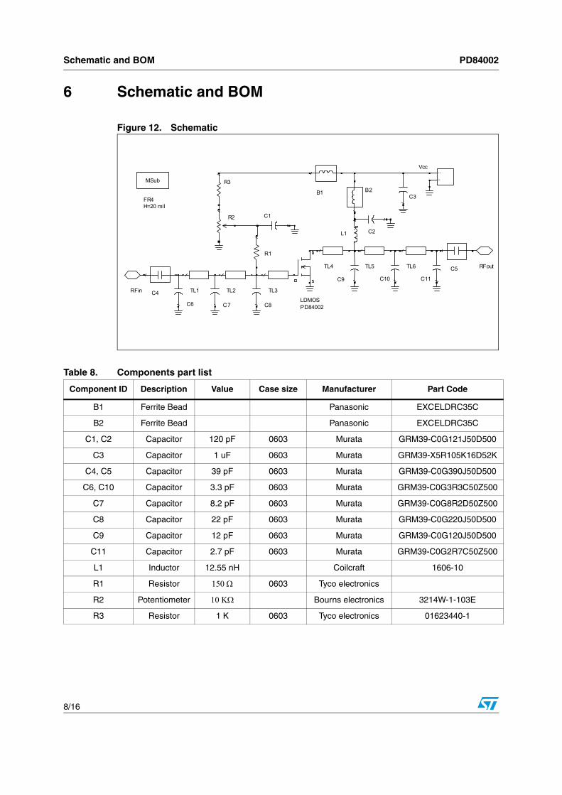
6 Schematic and BOM
Figure 12. Schematic
R2
PD84002LDMOS
TL3TL1 TL2C4RFin
R1
C6 C7 C8
R3
C1
C11
TL6 C5 RFout
C2
C9
Vcc
2 -
1 +
FR4H=20 mil
MSub
TL5TL4
B2
L1
C10
C3B1
Table 8. Components part list
Component ID Description Value Case size Manufacturer Part Code
B1 Ferrite Bead Panasonic EXCELDRC35C
B2 Ferrite Bead Panasonic EXCELDRC35C
C1, C2 Capacitor 120 pF 0603 Murata GRM39-C0G121J50D500
C3 Capacitor 1 uF 0603 Murata GRM39-X5R105K16D52K
C4, C5 Capacitor 39 pF 0603 Murata GRM39-C0G390J50D500
C6, C10 Capacitor 3.3 pF 0603 Murata GRM39-C0G3R3C50Z500
C7 Capacitor 8.2 pF 0603 Murata GRM39-C0G8R2D50Z500
C8 Capacitor 22 pF 0603 Murata GRM39-C0G220J50D500
C9 Capacitor 12 pF 0603 Murata GRM39-C0G120J50D500
C11 Capacitor 2.7 pF 0603 Murata GRM39-C0G2R7C50Z500
L1 Inductor 12.55 nH Coilcraft 1606-10
R1 Resistor 150 Ω 0603 Tyco electronics
R2 Potentiometer 10 KΩ Bourns electronics 3214W-1-103E
R3 Resistor 1 K 0603 Tyco electronics 01623440-1
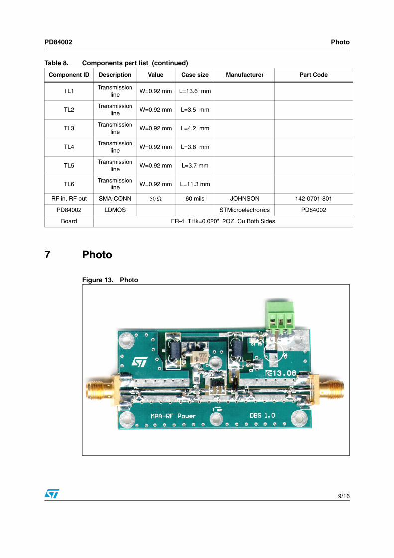
PD84002 Photo
9/16
7 Photo
Figure 13. Photo
Component ID Description Value Case size Manufacturer Part Code
TL1Transmission
lineW=0.92 mm L=13.6 mm
TL2Transmission
lineW=0.92 mm L=3.5 mm
TL3Transmission
lineW=0.92 mm L=4.2 mm
TL4Transmission
lineW=0.92 mm L=3.8 mm
TL5Transmission
lineW=0.92 mm L=3.7 mm
TL6Transmission
lineW=0.92 mm L=11.3 mm
RF in, RF out SMA-CONN 50 Ω 60 mils JOHNSON 142-0701-801
PD84002 LDMOS STMicroelectronics PD84002
Board FR-4 THk=0.020" 2OZ Cu Both Sides
Table 8. Components part list (continued)
Package mechanical data PD84002
10/16
8 Package mechanical data
In order to meet environmental requirements, ST offers these devices in ECOPACK® packages. These packages have a Lead-free second level interconnect . The category of second level interconnect is marked on the package and on the inner box label, in compliance with JEDEC Standard JESD97. The maximum ratings related to soldering conditions are also marked on the inner box label. ECOPACK is an ST trademark. ECOPACK specifications are available at: www.st.com

PD84002 Package mechanical data
11/16
Figure 14. Package dimensions
Table 9. SOT-89 mechanical data
Dim. mm. Inch
Min Typ Max Min Typ Max
A 1.4 1.6 55.1 63.0
B 0.44 0.56 17.3 22.0
B1 0.36 0.48 14.2 18.9
C 0.35 0.44 13.8 17.3
C1 0.35 0.44 13.8 17.3
D 4.4 4.6 173.2 181.1
D1 1.62 1.83 63.8 72.0
E 2.29 2.6 90.2 102.4
e 1.42 1.57 55.9 61.8
e1 2.92 3.07 115.0 120.9
H 3.94 4.25 155.1 167.3
L 0.89 1.2 35.0 47.2

Package mechanical data PD84002
12/16
8.1 Thermal pad and via designThernal vias are required in the PCB layout to effectively conduct heat away from the package. The via pattern has been designed to address thermal, power dissipation and electrical requirements of the device.
The via pattern is based on thru-hole vias with 0.203mm to 0.330mm finished hole size on a 0.5mm to 1.2mm grid pattern with 0.025 plating on via walls. If micro vias are used in a design, it is suggested that the quantity of vias be increased by a 4:1 ratio to achieve similar results.
Figure 15. Pad layout details

PD84002 Package mechanical data
13/16
8.2 Soldering profileFigure 16 shows the recommeded solder for devices that have Pb-free terminal plating and where a Pb-free solder is used.
Figure 16. Recommended solder profile
Figure 17 shows the recommeded solder for devices with Pb-free terminal plating used with leaded solder, or for devices with leaded terminal plating used with a leaded solder.
Figure 17. Recommended solder profile for leaded devices

Package mechanical data PD84002
14/16
Figure 18. Reel information
PD84002 Revision history
15/16
9 Revision history
Table 10. Document revision history
Date Revision Changes
05-Dec-2007 1 Initial release.
PD84002
16/16
Please Read Carefully:
Information in this document is provided solely in connection with ST products. STMicroelectronics NV and its subsidiaries (“ST”) reserve theright to make changes, corrections, modifications or improvements, to this document, and the products and services described herein at anytime, without notice.
All ST products are sold pursuant to ST’s terms and conditions of sale.
Purchasers are solely responsible for the choice, selection and use of the ST products and services described herein, and ST assumes noliability whatsoever relating to the choice, selection or use of the ST products and services described herein.
No license, express or implied, by estoppel or otherwise, to any intellectual property rights is granted under this document. If any part of thisdocument refers to any third party products or services it shall not be deemed a license grant by ST for the use of such third party productsor services, or any intellectual property contained therein or considered as a warranty covering the use in any manner whatsoever of suchthird party products or services or any intellectual property contained therein.
UNLESS OTHERWISE SET FORTH IN ST’S TERMS AND CONDITIONS OF SALE ST DISCLAIMS ANY EXPRESS OR IMPLIEDWARRANTY WITH RESPECT TO THE USE AND/OR SALE OF ST PRODUCTS INCLUDING WITHOUT LIMITATION IMPLIEDWARRANTIES OF MERCHANTABILITY, FITNESS FOR A PARTICULAR PURPOSE (AND THEIR EQUIVALENTS UNDER THE LAWSOF ANY JURISDICTION), OR INFRINGEMENT OF ANY PATENT, COPYRIGHT OR OTHER INTELLECTUAL PROPERTY RIGHT.
UNLESS EXPRESSLY APPROVED IN WRITING BY AN AUTHORIZED ST REPRESENTATIVE, ST PRODUCTS ARE NOTRECOMMENDED, AUTHORIZED OR WARRANTED FOR USE IN MILITARY, AIR CRAFT, SPACE, LIFE SAVING, OR LIFE SUSTAININGAPPLICATIONS, NOR IN PRODUCTS OR SYSTEMS WHERE FAILURE OR MALFUNCTION MAY RESULT IN PERSONAL INJURY,DEATH, OR SEVERE PROPERTY OR ENVIRONMENTAL DAMAGE. ST PRODUCTS WHICH ARE NOT SPECIFIED AS "AUTOMOTIVEGRADE" MAY ONLY BE USED IN AUTOMOTIVE APPLICATIONS AT USER’S OWN RISK.
Resale of ST products with provisions different from the statements and/or technical features set forth in this document shall immediately voidany warranty granted by ST for the ST product or service described herein and shall not create or extend in any manner whatsoever, anyliability of ST.
ST and the ST logo are trademarks or registered trademarks of ST in various countries.
Information in this document supersedes and replaces all information previously supplied.
The ST logo is a registered trademark of STMicroelectronics. All other names are the property of their respective owners.
© 2007 STMicroelectronics - All rights reserved
STMicroelectronics group of companies
Australia - Belgium - Brazil - Canada - China - Czech Republic - Finland - France - Germany - Hong Kong - India - Israel - Italy - Japan - Malaysia - Malta - Morocco - Singapore - Spain - Sweden - Switzerland - United Kingdom - United States of America
www.st.com