RF Power Field Effect Transistors N--Channel Enhancement ...
27
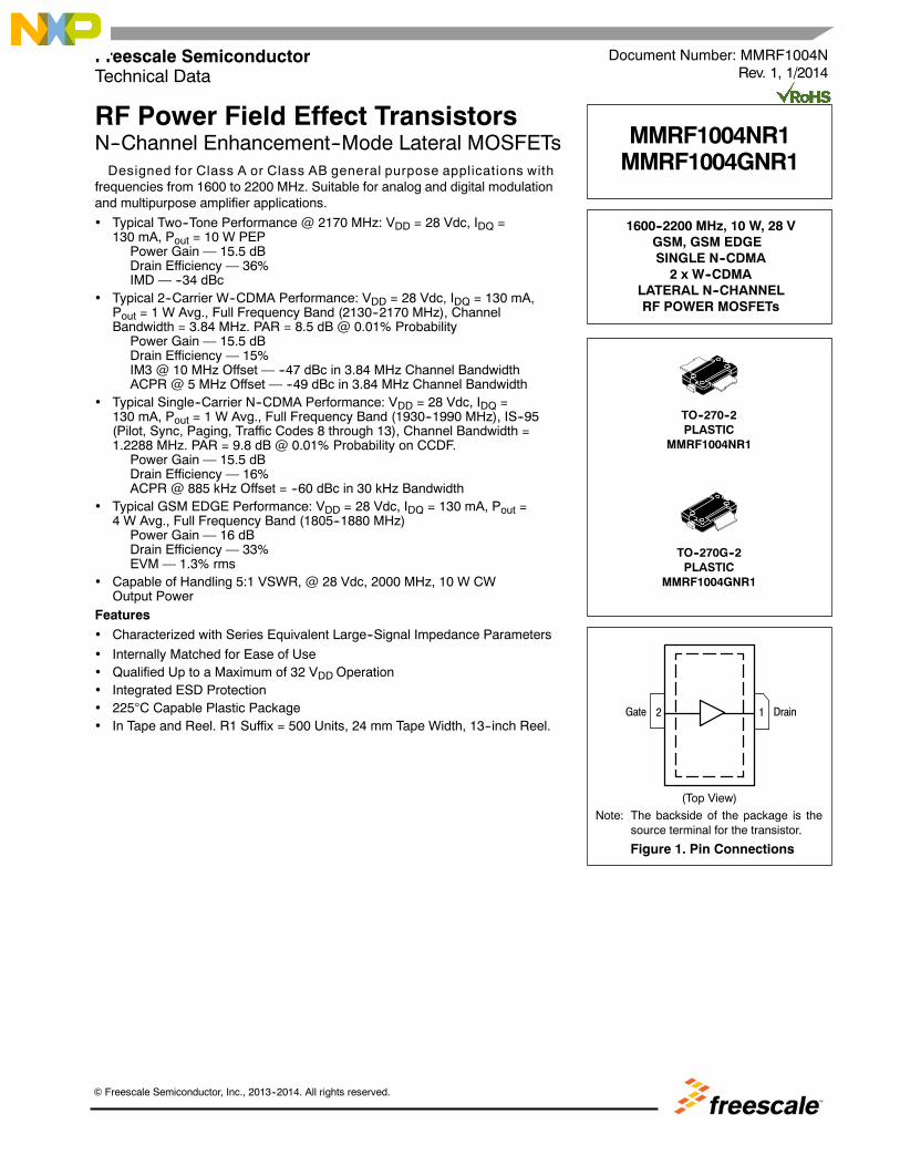
RF Power Field Effect Transistors N--Channel Enhancement--ModeLateral MOSFETs Designed for Class A or Class AB general purpose applications with frequencies from 1600 to 2200 MHz. Suitable for analog and digital modulation and multipurpose amplifier applications. Typical Two--Tone Performance @ 2170 MHz: V DD = 28 Vdc, I DQ = 130 mA, P out = 10 W PEP Power Gain — 15.5 dB Drain Efficiency — 36% IMD — --34 dBc Typical 2--Carrier W--CDMA Performance: V DD = 28 Vdc, I DQ = 130 mA, P out = 1 W Avg., Full Frequency Band (2130--2170 MHz), Channel Bandwidth = 3.84 MHz. PAR = 8.5 dB @ 0.01% Probability Power Gain — 15.5 dB Drain Efficiency — 15% IM3 @ 10 MHz Offset — --47 dBc in 3.84 MHz Channel Bandwidth ACPR @ 5 MHz Offset — --49 dBc in 3.84 MHz Channel Bandwidth Typical Single--Carrier N--CDMA Performance: V DD = 28 Vdc, I DQ = 130 mA, P out = 1 W Avg., Full Frequency Band (1930--1990 MHz), IS--95 (Pilot, Sync, Paging, Traffic Codes 8 through 13), Channel Bandwidth = 1.2288 MHz. PAR = 9.8 dB @ 0.01% Probability on CCDF. Power Gain — 15.5 dB Drain Efficiency — 16% ACPR @ 885 kHz Offset = --60 dBc in 30 kHz Bandwidth Typical GSM EDGE Performance: V DD = 28 Vdc, I DQ = 130 mA, P out = 4 W Avg., Full Frequency Band (1805--1880 MHz) Power Gain — 16 dB Drain Efficiency — 33% EVM — 1.3% rms Capable of Handling 5:1 VSWR, @ 28 Vdc, 2000 MHz, 10 W CW Output Power Features Characterized with Series Equivalent Large--Signal Impedance Parameters Internally Matched for Ease of Use Qualified Up to a Maximum of 32 V DD Operation Integrated ESD Protection 225C Capable Plastic Package In Tape and Reel. R1 Suffix = 500 Units, 24 mm Tape Width, 13--inch Reel. Document Number: MMRF1004N Rev. 1, 1/2014 Freescale Semiconductor Technical Data (Top View) Drain 2 1 Gate 1600--2200 MHz, 10 W, 28 V GSM, GSM EDGE SINGLE N--CDMA 2 x W--CDMA LATERAL N--CHANNEL RF POWER MOSFETs MMRF1004NR1 MMRF1004GNR1 TO--270--2 PLASTIC MMRF1004NR1 TO--270G--2 PLASTIC MMRF1004GNR1 Figure 1. Pin Connections Note: The backside of the package is the source terminal for the transistor. Freescale Semiconductor, Inc., 2013--2014. All rights reserved.
Transcript of RF Power Field Effect Transistors N--Channel Enhancement ...
1RF Device DataFreescale Semiconductor
RF Power Field Effect TransistorsN--Channel Enhancement--Mode Lateral MOSFETsDesigned for Class A or Class AB general purpose applications with
frequencies from 1600 to 2200 MHz. Suitable for analog and digital modulationand multipurpose amplifier applications.
Typical Two--Tone Performance @ 2170 MHz: VDD = 28 Vdc, IDQ =130 mA, Pout = 10 W PEP
Power Gain — 15.5 dBDrain Efficiency — 36%IMD — --34 dBc
Typical 2--Carrier W--CDMA Performance: VDD = 28 Vdc, IDQ = 130 mA,Pout = 1 W Avg., Full Frequency Band (2130--2170 MHz), ChannelBandwidth = 3.84 MHz. PAR = 8.5 dB @ 0.01% Probability
Power Gain — 15.5 dBDrain Efficiency — 15%IM3 @ 10 MHz Offset — --47 dBc in 3.84 MHz Channel BandwidthACPR @ 5 MHz Offset — --49 dBc in 3.84 MHz Channel Bandwidth
Typical Single--Carrier N--CDMA Performance: VDD = 28 Vdc, IDQ =130 mA, Pout = 1 W Avg., Full Frequency Band (1930--1990 MHz), IS--95(Pilot, Sync, Paging, Traffic Codes 8 through 13), Channel Bandwidth =1.2288 MHz. PAR = 9.8 dB @ 0.01% Probability on CCDF.
Power Gain — 15.5 dBDrain Efficiency — 16%ACPR @ 885 kHz Offset = --60 dBc in 30 kHz Bandwidth
Typical GSM EDGE Performance: VDD = 28 Vdc, IDQ = 130 mA, Pout =4 W Avg., Full Frequency Band (1805--1880 MHz)
Power Gain — 16 dBDrain Efficiency — 33%EVM — 1.3% rms
Capable of Handling 5:1 VSWR, @ 28 Vdc, 2000 MHz, 10 W CWOutput Power
Features Characterized with Series Equivalent Large--Signal Impedance Parameters
Internally Matched for Ease of Use Qualified Up to a Maximum of 32 VDD Operation Integrated ESD Protection 225C Capable Plastic Package In Tape and Reel. R1 Suffix = 500 Units, 24 mm Tape Width, 13--inch Reel.
Document Number: MMRF1004NRev. 1, 1/2014
Freescale SemiconductorTechnical Data
(Top View)
Drain2 1Gate
1600--2200 MHz, 10 W, 28 VGSM, GSM EDGESINGLE N--CDMA2 x W--CDMA
LATERAL N--CHANNELRF POWER MOSFETs
MMRF1004NR1MMRF1004GNR1
TO--270--2PLASTIC
MMRF1004NR1
TO--270G--2PLASTIC
MMRF1004GNR1
Figure 1. Pin Connections
Note: The backside of the package is thesource terminal for the transistor.
Freescale Semiconductor, Inc., 2013--2014. All rights reserved.

2RF Device Data
Freescale Semiconductor
MMRF1004NR1 MMRF1004GNR1
Table 1. Maximum Ratings
Rating Symbol Value Unit
Drain--Source Voltage VDSS --0.5, +68 Vdc
Gate--Source Voltage VGS --0.5, +12 Vdc
Storage Temperature Range Tstg --65 to +150 C
Case Operating Temperature TC 150 C
Operating Junction Temperature (1) TJ 225 C
Table 2. Thermal Characteristics
Characteristic Symbol Value (2) Unit
Thermal Resistance, Junction to CaseCase Temperature 78C, 1 W CWCase Temperature 79C, 10 W PEP, Two--Tone Test
RJC2.32.9
C/W
Table 3. ESD Protection Characteristics
Test Methodology Class
Human Body Model (per JESD22--A114) 1A
Machine Model (per EIA/JESD22--A115) A
Charge Device Model (per JESD22--C101) IV
Table 4. Moisture Sensitivity Level
Test Methodology Rating Package Peak Temperature Unit
Per JESD22--A113, IPC/JEDEC J--STD--020 3 260 C
Table 5. Electrical Characteristics (TA = 25C unless otherwise noted)
Characteristic Symbol Min Typ Max Unit
Off Characteristics
Zero Gate Voltage Drain Leakage Current(VDS = 68 Vdc, VGS = 0 Vdc)
IDSS — — 10 Adc
Zero Gate Voltage Drain Leakage Current(VDS = 28 Vdc, VGS = 0 Vdc)
IDSS — — 1 Adc
Gate--Source Leakage Current(VGS = 5 Vdc, VDS = 0 Vdc)
IGSS — — 500 Adc
On Characteristics
Gate Threshold Voltage(VDS = 10 Vdc, ID = 40 Adc)
VGS(th) 1.5 2.2 3.5 Vdc
Gate Quiescent Voltage(VDD = 28 Vdc, ID = 130 mAdc, Measured in Functional Test)
VGS(Q) 2 2.8 4 Vdc
Drain--Source On--Voltage(VGS = 10 Vdc, ID = 0.4 Adc)
VDS(on) — 0.33 0.4 Vdc
Dynamic Characteristics (4)
Output Capacitance(VDS = 28 Vdc 30 mV(rms)ac @ 1 MHz, VGS = 0 Vdc)
Coss — 20 — pF
Reverse Transfer Capacitance(VDS = 28 Vdc 30 mV(rms)ac @ 1 MHz, VGS = 0 Vdc)
Crss — 11.6 — pF
Input Capacitance(VDS = 28 Vdc, VGS = 0 Vdc 30 mV(rms)ac @ 1 MHz)
Ciss — 120 — pF
1. Continuous use at maximum temperature will affect MTTF.2. Refer to AN1955, Thermal Measurement Methodology of RF Power Amplifiers. Go to http://www.freescale.com/rf.
Select Documentation/Application Notes -- AN1955.3. Part internally matched on input.
(continued)
MMRF1004NR1 MMRF1004GNR1
3RF Device DataFreescale Semiconductor
Table 5. Electrical Characteristics (TA = 25C unless otherwise noted) (continued)
Characteristic Symbol Min Typ Max Unit
Functional Tests (1) (In Freescale Test Fixture, 50 ohm system) VDD = 28 Vdc, IDQ = 130 mA, Pout = 10 W PEP, f1 = 2170 MHz,f2 = 2170.1 MHz, Two--Tone Test
Power Gain Gps 14 15.5 17 dB
Drain Efficiency D 33 36 — %
Intermodulation Distortion IMD — --34 --28 dBc
Input Return Loss IRL — --15 --9 dB
Typical 2--Carrier W--CDMA Performances (In Freescale CDMA Test Fixture, 50 ohm system) VDD = 28 Vdc, IDQ = 130 mA, Pout =1 W Avg., f1 = 2112.5 MHz, f2 = 2122.5 MHz and f1 = 2157.5 MHz, f2 = 2167.5 MHz, 2--Carrier W--CDMA, 3.84 MHz Channel BandwidthCarriers. ACPR measured in 3.84 MHz Channel Bandwidth @ 5 MHz Offset. IM3 measured in 3.84 MHz Bandwidth @ 10 MHz Offset.PAR = 8.5 dB @ 0.01% Probability on CCDF.
Power Gain Gps — 15.5 — dB
Drain Efficiency D — 15 — %
Gain Flatness in 30 MHz Bandwidth @ Pout = 1 W CW GF — 0.3 — dB
Intermodulation Distortion IM3 — --47 — dBc
Adjacent Channel Power Ratio ACPR — --49 — dBc
Typical N--CDMA Performances (In Freescale Test Fixture, 50 ohm system) VDD = 28 Vdc, IDQ = 130 mA, Pout = 1 W Avg.,1930 MHz<Frequency<1990 MHz, Single--Carrier N--CDMA, 1.2288 MHz Channel Bandwidth Carrier. ACPR measured in 30 kHz ChannelBandwidth @ 885 kHz Offset. PAR = 9.8 dB @ 0.01% Probability on CCDF
Power Gain Gps — 15.5 — dB
Drain Efficiency D — 16 — %
Gain Flatness in 30 MHz Bandwidth @ Pout = 1 W CW GF — 0.3 — dB
Adjacent Channel Power Ratio ACPR — --60 — dBc
Typical GSM EDGE Performances (In Freescale GSM EDGE Test Fixture, 50 hm system) VDD = 28 Vdc, IDQ = 130 mA, Pout = 4 W Avg.,1805--1880 MHz, EDGE Modulation
Power Gain Gps — 16 — dB
Drain Efficiency D — 33 — %
Gain Flatness in 30 MHz Bandwidth @ Pout = 4 W CW GF — 0.3 — dB
Error Vector Magnitude EVM — 1.3 — % rms
Spectral Regrowth at 400 kHz Offset SR1 — --60 — dBc
Spectral Regrowth at 600 kHz Offset SR2 — --70 — dBc
1. Measurements made with device in straight lead configuration before any lead forming operation is applied. Lead forming is used for gullwing (GN) parts.

4RF Device Data
Freescale Semiconductor
MMRF1004NR1 MMRF1004GNR1
Figure 2. MMRF1004NR1 Test Circuit Schematic — 2110--2170 MHz
Z10 0.930 x 0.350 MicrostripZ11 0.930 x 0.400 MicrostripZ12 0.050 x 0.105 MicrostripZ13 0.405 x 0.242 MicrostripZ14 0.066 x 0.740 MicrostripZ16, Z17 0.050 x 1.250 MicrostripPCB Taconic RF--35, 0.030, r = 3.5
Z1, Z15 0.066 x 0.480 MicrostripZ2 0.066 x 0.765 MicrostripZ3, Z5 0.066 x 0.340 x 0.050 TaperZ4 0.340 x 0.295 MicrostripZ6 0.020 x 0.060 MicrostripZ7 0.0905 x 0.280 MicrostripZ8 0.0905 x 0.330 MicrostripZ9 0.050 x 0.980 Microstrip
RFOUTPUT
VBIAS VSUPPLY
RFINPUT
DUT
Z1
C2
R1
C11
+
C1 C7R2 Z9
R3
Z2 Z3 Z4 Z5 Z6 Z7 Z8
Z10
Z16
C3 C4 C5
Z11 Z12 Z13 Z14
C6
Z15
Z17
C8 C9 C10
Table 6. MMRF1004NR1 Test Circuit Component Designations and Values — 2110--2170 MHz
Part Description Part Number Manufacturer
C1 100 nF Chip Capacitor CDR33BX104AKYS Kemet
C2, C6 4.7 pF Chip Capacitors ATC100B4R7CT500XT ATC
C3, C7, C8 9.1 pF Chip Capacitors ATC100B9R1CT500XT ATC
C4, C5, C9, C10 10 F, 50 V Chip Capacitors GRM55DR61H106KA88B Murata
C11 10 F, 35 V Tantalum Chip Capacitor T490D106K035AT Kemet
R1 1 k, 1/4 W Chip Resistor CRCW12061001FKEA Vishay
R2 10 k, 1/4 W Chip Resistor CRCW12061002FKEA Vishay
R3 10 , 1/4 W Chip Resistor CRCW120610R0FKEA Vishay

MMRF1004NR1 MMRF1004GNR1
5RF Device DataFreescale Semiconductor
Figure 3. MMRF1004NR1 Test Circuit Component Layout — 2110--2170 MHz
CUTOUTAREA
R1
C11R2 C1
C7R3
C2
C3C4 C5
C6
C8
C9 C10
6RF Device Data
Freescale Semiconductor
MMRF1004NR1 MMRF1004GNR1
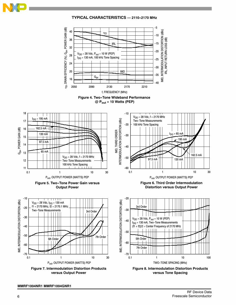
TYPICAL CHARACTERISTICS — 2110--2170 MHz
2210
16
40
2050--40
--5
IRL
Gps
IMD
f, FREQUENCY (MHz)
VDD = 28 Vdc, Pout = 10 W (PEP)IDQ = 130 mA, 100 kHz Tone Spacing
36--10
32--15
28
24
--20
--25
20--30
2130 2170
Figure 4. Two--Tone Wideband Performance@ Pout = 10 Watts (PEP)
Pout, OUTPUT POWER (WATTS) PEP
11
18
1
IDQ = 195 mA
VDD = 28 Vdc, f = 2170 MHzTwo--Tone Measurements100 kHz Tone Spacing
17
14
12
10 30
Figure 5. Two--Tone Power Gain versusOutput Power
30--60
--10
0.1 1 10
--20
--30
--40
--50
Pout, OUTPUT POWER (WATTS) PEP
Figure 6. Third Order IntermodulationDistortion versus Output Power
Gps,POWER
GAIN(dB)
IRL,INPUTRETURNLOSS
(dB)
IMD,INTERMODULATIONDISTORTION(dBc)
10--70
--10
0.1
7th Order
VDD = 28 Vdc, IDQ = 130 mAf1 = 2170 MHz, f2 = 2170.1 MHzTwo--Tone Measurements
5th Order
3rd Order--20
--30
--40
1 30
Figure 7. Intermodulation Distortion Productsversus Output Power
IMD,INTERMODULATIONDISTORTION(dBc)
2090
15
65 mA
130 mA
--50
--35
0.1
D,DRAINEFFICIENCY(%),Gps,POWER
GAIN(dB)
D
16
13
97.5 mA
162.5 mA
INTERMODULATIONDISTORTION(dBc)
IMD,THIRDORDER
130 mA97.5 mA
195 mA
10--70
--20
0.1
7th Order
TWO--TONE SPACING (MHz)
VDD = 28 Vdc, Pout = 10 W (PEP)IDQ = 130 mA, Two--Tone Measurements(f1 + f2)/2 = Center Frequency of 2170 MHz
5th Order
3rd Order--30
--40
--50
1 100
Figure 8. Intermodulation Distortion Productsversus Tone Spacing
IMD,INTERMODULATIONDISTORTION(dBc)
--60
Pout, OUTPUT POWER (WATTS) PEP
--60
VDD = 28 Vdc, f = 2170 MHzTwo--Tone Measurements100 kHz Tone Spacing
162.5 mA
IDQ = 65 mA

MMRF1004NR1 MMRF1004GNR1
7RF Device DataFreescale Semiconductor
TYPICAL CHARACTERISTICS — 2110--2170 MHz
30
47
P3dB = 41.5 dBm (14.2 W)
Pin, INPUT POWER (dBm)
VDD = 28 Vdc, IDQ = 130 mAPulsed CW, 8 sec(on), 1 msec(off)f = 2170 MHz
45
43
41
39
3522 24 26
Actual
Ideal
2820
Figure 9. Pulsed CW Output Power versusInput Power
P out,OUTPUTPOWER
(dBm
)
P1dB = 40.9 dBm (12.26 W)
3011
18
0.10
70
TC = --30_C
25_C--30_C
101
16
15
14
12
50
40
20
10
Pout, OUTPUT POWER (WATTS) CW
Figure 10. Power Gain and Drain Efficiencyversus CW Output Power
Gps,POWER
GAIN(dB)
Gps
85_C
25_C
85_C
VDD = 28 VdcIDQ = 130 mAf = 2170 MHz
D
DDRAINEFFICIENCY(%)
Pout, OUTPUT POWER (WATTS) CW
Figure 11. Power Gain versus Output Power
IDQ = 130 mAf = 2170 MHz
10
16
0 18
13
11
14
6 9 12
Gps,POWER
GAIN(dB)
21153
VDD = 24 V28 V
32 V
--36
27
400--15
6
S21
f, FREQUENCY (MHz)
Figure 12. Broadband Frequency Response
S11
18 3
9 0
0 --3
--18
--6
--27 --12
320028002400200016001200800
VDD = 28 VdcPout = 10 W (PEP)IDQ = 130 mA
S11(dB)
S21(dB)
37
17
13
60
30
15
12
--9
--9
This above graph displays calculated MTTF in hours when the deviceis operated at VDD = 28 and D = 47.2%.
MTTF calculator available at http://www.freescale.com/rf. SelectSoftware & Tools/Development Tools/Calculators to access MTTFcalculators by product.
250
108
90TJ, JUNCTION TEMPERATURE (C)
Figure 13. MTTF versus Junction Temperature — CW
107
106
104
110 130 150 170 190
MTTF(HOURS)
210 230
105
108108

8RF Device Data
Freescale Semiconductor
MMRF1004NR1 MMRF1004GNR1
W--CDMA TYPICAL CHARACTERISTICS — 2110--2170 MHz
Gps,POWER
GAIN(dB)
IRL,INPUTRETURNLOSS
(dB)
IM3(dBc),ACPR
(dBc)
--18
--10
--12
--16
22202060
IRL
Gps
ACPR
IM3
f, FREQUENCY (MHz)
Figure 14. 2--Carrier W--CDMA Broadband Performance@ Pout = 1 Watt Avg.
2200218021602140212021002080
16
--55
18
17
16
15
--45
--47
--49
D,DRAIN
EFFICIENCY(%)
15.8
15.6
15.4
15.2
15
14.8
14.6
--51--14
14
DVDD = 28 Vdc, Pout = 1 W (Avg.), IDQ = 130 mA2--Carrier W--CDMA, 10 MHz Carrier Spacing3.84 MHz Channel Bandwidth, PAR = 8.5 dB@ 0.01% Probability (CCDF)
14.4
14.2
14
--53
IM3(dBc),ACPR
(dBc)
Figure 15. 2--Carrier W--CDMA ACPR, IM3, Power Gainand Drain Efficiency versus Output Power
0 --55
Pout, OUTPUT POWER (WATTS) AVG.
49 --20
--3035
28 --35
14
1 20
--40
IM3
Gps
D,DRAINEFFICIENCY(%),Gps,POWER
GAIN(dB)
42
--45
D
ACPR
0.1
--25
21TC = 25_C
VDD = 28 Vdc, IDQ = 130 mAf1 = 2165 MHz, f2 = 2175 MHz2--Carrier W--CDMA, 10 MHz CarrierSpacing, 3.84 MHz ChannelBandwidth, PAR = 8.5 dB@ 0.01% Probability (CCDF)
7 --50
10

MMRF1004NR1 MMRF1004GNR1
9RF Device DataFreescale Semiconductor
W--CDMA TEST SIGNAL
100.0001
100
0
PEAK--TO--AVERAGE (dB)
Figure 16. CCDF W--CDMA 3GPP, Test Model 1,64 DPCH, 67% Clipping, Single--Carrier Test Signal
10
1
0.1
0.01
0.001
2 4 6 8
Figure 17. 2-Carrier W-CDMA Spectrum
f, FREQUENCY (MHz)
3.84 MHzChannel BW
--IM3 in3.84 MHz BW
+IM3 in3.84 MHz BW
--ACPR in3.84 MHz BW
+ACPR in3.84 MHz BW
PROBABILITY
(%)
(dB)
+20
+30
0
--10
--40
--50
--60
--70
--80
--20
205 15100--5--10--15--20--25 25
--30W--CDMA. ACPR Measured in 3.84 MHz ChannelBandwidth @ 5 MHz Offset. IM3 Measured in3.84 MHz Bandwidth @ 10 MHz Offset. PAR =8.5 dB @ 0.01% Probability on CCDF

10RF Device Data
Freescale Semiconductor
MMRF1004NR1 MMRF1004GNR1
N--CDMA TYPICAL CHARACTERISTICS — 1930--1990 MHz
RFOUTPUT
VBIAS VSUPPLY
RFINPUT
DUT
Z1
C2
R1
C11
+
C1 C7R2 Z7
R3
Z2 Z3 Z4 Z5 Z6
Z8
Z17
C3 C4 C5
Z11 Z12 Z13 Z14
C6
Z16
Z18
C8 C9 C10
Z9 Z10 Z15
Figure 18. MMRF1004NR1 Test Circuit Schematic — 1930--1990 MHz
Z11 0.244 x 0.423 MicrostripZ12 0.244 x 0.066 x 0.089 TaperZ13 0.066 x 0.182 MicrostripZ14 0.066 x 0.263 MicrostripZ15 0.236 x 0.118 MicrostripZ16 0.066 x 0.099 MicrostripZ17, Z18 0.050 x 1.250 MicrostripPCB Taconic RF--35, 0.030, r = 3.5
Z1 0.066 x 0.480 MicrostripZ2 0.066 x 0.728 MicrostripZ3 0.354 x 0.512 MicrostripZ4 0.066 x 0.079 MicrostripZ5, Z6 0.591 x 0.335 MicrostripZ7 0.050 x 0.980 MicrostripZ8 1.142 x 0.350 MicrostripZ9 1.142 x 0.516 MicrostripZ10 0.433 x 0.276 Microstrip
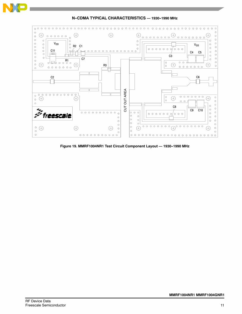
Table 7. MMRF1004NR1 Test Circuit Component Designations and Values — 1930--1990 MHz
Part Description Part Number Manufacturer
C1 100 nF Chip Capacitor 12065C104KAT AVX
C2, C6 4.7 pF Chip Capacitors ATC100B4R7BT500XT ATC
C3, C7, C8 9.1 pF Chip Capacitors ATC100B9R1BT500XT ATC
C4, C5, C9, C10 10 F Chip Capacitors C5750X5R1H106MT TDK
C11 10 F, 35 V Tantalum Chip Capacitor TAJD106K035R AVX
R1, R2 10 k, 1/4 W Chip Resistors CRCW12061002FKEA Vishay
R3 10 , 1/4 W Chip Resistor CRCW120610R0FKEA Vishay
MMRF1004NR1 MMRF1004GNR1
11RF Device DataFreescale Semiconductor
N--CDMA TYPICAL CHARACTERISTICS — 1930--1990 MHz
Figure 19. MMRF1004NR1 Test Circuit Component Layout — 1930--1990 MHz
CUTOUTAREA
C11
VDD VGS
R1
R2 C1
C7
R3
C2
C3C4 C5
C6
C9 C10C8
12RF Device Data
Freescale Semiconductor
MMRF1004NR1 MMRF1004GNR1
N--CDMA TYPICAL CHARACTERISTICS — 1930--1990 MHz
Gps,POWER
GAIN(dB)
IRL,INPUTRETURNLOSS
(dB)
ACPR
(dBc)
--20
--8
--11
--17
20001900
Gps
ACPR
f, FREQUENCY (MHz)
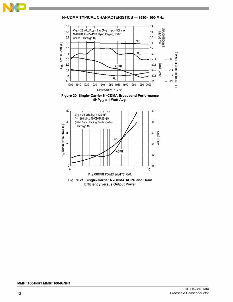
Figure 20. Single--Carrier N--CDMA Broadband Performance@ Pout = 1 Watt Avg.
1970196019501940193019201910
15.9
--61
19
18
17
16
--59.4
--59.8
D,DRAIN
EFFICIENCY(%)
15.8
15.7
15.6
15.5
15.3
--60.2 --14
14.9
D
VDD = 28 Vdc, Pout = 1 W (Avg.), IDQ = 500 mAN--CDMA IS--95 (Pilot, Sync, Paging, TrafficCodes 8 Through 13)
15.1
15
--60.6
15.4
15.2
15
1980 1990
IRL
--59
ACPR
(dBc)
Figure 21. Single--Carrier N--CDMA ACPR and DrainEfficiency versus Output Power
0 --65
Pout, OUTPUT POWER (WATTS) AVG.
50 --40
--5030
--5520
1
D,DRAINEFFICIENCY(%) 40
D
ACPR
0.1
--45
VDD = 28 Vdc, IDQ = 130 mAf = 1960 MHz, N--CDMA IS--95(Pilot, Sync, Paging, Traffic Codes8 Through 13)
10 --60
10

MMRF1004NR1 MMRF1004GNR1
13RF Device DataFreescale Semiconductor
N--CDMA TEST SIGNAL
100.0001
100
0
PEAK--TO--AVERAGE (dB)
Figure 22. Single--Carrier CCDF N--CDMA
10
1
0.1
0.01
0.001
2 4 6 8
IS--95 CDMA (Pilot, Sync, Paging, Traffic Codes 8Through 13) 1.2288 MHz Channel BandwidthCarriers. ACPR Measured in 30 kHz Bandwidth @885 kHz Offset. PAR = 9.8 dB @ 0.01% Probabilityon CCDF.
PROBABILITY
(%)
.................
... ....... ......... ...... .................................
.
.......
...
......... ..... .............. ..... ... ... ..... . .... ..... .. ................ ..........................................
............... ........... ....... ................................ ............. ........... ... ... ... ............................... ............... .... .. .................... ..... .... ................... . .. . ..... .... .... .. ....... ......... .. ... ... .. . ....... ... .......... .. .. .. ..
... ...... ............ .. ....
.............. .... ............................................. .................................... ... .... .....
... .............. ....
.. ... ............... .. ..... .. ..... ....... ................. ....... ........... ... .
.............................. ........................................ ....................... ....... ............................ ....... ......................... ......... .
.................. .... ..............
......
....
..
..
..
....
....
..... ... ... .............. ...... ... ... .... .. ... .......... .. .... ................... ...... ..............
................
.................
............
.
. .. ............... ... .. . ...
.........................................................
.....
--60
--110
--10
(dB)
--20
--30
--40
--50
--70
--80
--90
--100
+ACPR in 30 kHzIntegrated BW
1.2288 MHzChannel BW
2.90.7 2.21.50--0.7--1.5--2.2--2.9--3.6 3.6
f, FREQUENCY (MHz)
Figure 23. Single--Carrier N--CDMA Spectrum
--ACPR in 30 kHzIntegrated BW

14RF Device Data
Freescale Semiconductor
MMRF1004NR1 MMRF1004GNR1
GSM EDGE TYPICAL CHARACTERISTICS — 1805--1880 MHz
RFOUTPUT
VBIAS VSUPPLY
RFINPUT
DUT
Z1
C2
R1
C11
+
C1 C7R2 Z9
R3
Z2 Z3 Z4 Z5 Z8
Z10
Z17
C3 C4 C5
Z11 Z12 Z13 Z14
C6
Z16
Z18
C8 C9 C10
Z15
Figure 24. MMRF1004NR1 Test Circuit Schematic — 1805--1880 MHz
Z10 1.142 x 0.350 MicrostripZ11 1.142 x 0.516 MicrostripZ12 0.433 x 0.276 MicrostripZ13 0.276 x 0.157 MicrostripZ14 0.236 x 0.433 MicrostripZ15 0.066 x 0.104 MicrostripZ17, Z18 0.050 x 1.250 MicrostripPCB Taconic RF--35, 0.030, r = 3.5
Z1, Z16 0.066 x 0.480 MicrostripZ2 0.066 x 0.137 MicrostripZ3 0.236 x 0.236 MicrostripZ4 0.066 x 0.354 MicrostripZ5 0.551 x 0.512 MicrostripZ6 0.066 x 0.079 MicrostripZ7 0.591 x 0.189 MicrostripZ8 0.591 x 0.334 MicrostripZ9 0.050 x 0.980 Microstrip
Z7Z6
Table 8. MMRF1004NR1 Test Circuit Component Designations and Values —1805--1880 MHz
Part Description Part Number Manufacturer
C1 100 nF Chip Capacitor 12065C104KAT AVX
C2, C6 4.7 pF Chip Capacitors ATC100B4R7BT500XT ATC
C3, C7, C8 9.1 pF Chip Capacitors ATC100B9R1BT500XT ATC
C4, C5, C9, C10 10 F Chip Capacitors C5750X5R1H106MT TDK
C11 10 F, 35 V Tantalum Chip Capacitor TAJD106K035R AVX
R1, R2 10 k, 1/4 W Chip Resistors CRCW12061001FKEA Vishay
R3 10 , 1/4 W Chip Resistor CRCW120610R0FKEA Vishay

MMRF1004NR1 MMRF1004GNR1
15RF Device DataFreescale Semiconductor
GSM EDGE TYPICAL CHARACTERISTICS — 1805--1880 MHz
Figure 25. MMRF1004NR1 Test Circuit Component Layout — 1805--1880 MHz
CUTOUTAREA
C11
VDD VGS
R1
R2 C1
C7
R3
C2
C3C4 C5
C6
C9 C10C8
16RF Device Data
Freescale Semiconductor
MMRF1004NR1 MMRF1004GNR1
GSM EDGE TYPICAL CHARACTERISTICS — 1805--1880 MHz
Gps,POWER
GAIN(dB)
IRL,INPUTRETURNLOSS
(dB)
f, FREQUENCY (MHz)
131800
10
Gps
VDD = 28 VdcIDQ = 130 mA
17 50
16 40
15 30
14 20
1900
IRL
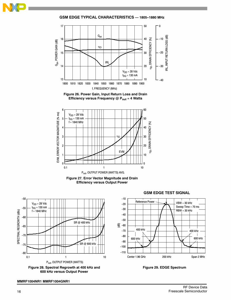
Figure 26. Power Gain, Input Return Loss and DrainEfficiency versus Frequency @ Pout = 4 Watts
--30
0
--10
--20
--40
D
D,DRAINEFFICIENCY(%)
1810 1820 1830 1840 1850 1860 1870 1880 1890
Figure 27. Error Vector Magnitude and DrainEfficiency versus Output Power
Pout, OUTPUT POWER (WATTS) AVG.
10
2
6
VDD = 28 VdcIDQ = 130 mAf = 1840 MHz
4
3
010.1
1
20
60
40
30
0
10EVM
D
D,DRAINEFFICIENCY(%)
EVM,ERRORVECTORMAGNITUDE(%
ms)
505
10--80
--50
0.1
Pout, OUTPUT POWER (WATTS)
--55
--60
--65
--70
--75
1
VDD = 28 VdcIDQ = 130 mAf = 1840 MHz
Figure 28. Spectral Regrowth at 400 kHz and600 kHz versus Output Power
SPECTRAL
REGROWTH
(dBc)
SR @ 400 kHz
SR @ 600 kHz
Figure 29. EDGE Spectrum
--10
--20
--30
--40
--50
--60
--70
--80
--90
--100
200 kHz Span 2 MHzCenter 1.96 GHz
--110
400 kHz
600 kHz
400 kHz
600 kHz
(dB)
Reference Power VBW = 30 kHzSweep Time = 70 msRBW = 30 kHz
GSM EDGE TEST SIGNAL

MMRF1004NR1 MMRF1004GNR1
17RF Device DataFreescale Semiconductor
Figure 30. Series Equivalent Source and Load Impedance
Zsource = Test circuit impedance as measured fromgate to ground.
Zload = Test circuit impedance as measuredfrom drain to ground.
Zsource Z load
InputMatchingNetwork
DeviceUnderTest
OutputMatchingNetwork
f = 1880 MHz
Zo = 25
ZloadZsource
fMHz
Zsource
Zload
1805
1840
1880
13.237 + j5.810
14.858 + j6.279
13.953 + j6.084
2.445 + j3.698
2.542 + j3.942
2.695 + j4.170
VDD = 28 Vdc, IDQ = 130 mA, Pout = 4 W Avg.
1800 MHz
fMHz
Zsource
Zload
2110
2140
2170
3.619 + j0.792
4.087 + j0.558
3.918 + j0.797
2.544 + j3.068
2.673 + j3.291
2.818 + j3.406
VDD = 28 Vdc, IDQ = 130 mA, Pout = 10 W PEP
2170 MHz
fMHz
Zsource
Zload
1930
1960
1990
9.237 + j1.849
9.889 + j2.434
9.521 + j2.144
2.770 + j3.497
2.754 + j3.668
2.772 + j3.833
VDD = 28 Vdc, IDQ = 130 mA, Pout = 1 W Avg.
1900 MHz
f = 1805 MHzf = 1805 MHz
f = 1880 MHz
f = 1930 MHz
f = 1990 MHz
Zload
Zsource
Zo = 25
f = 1990 MHz
f = 1930 MHz
f = 2110 MHz
Zsource
Zload
f = 2170 MHz
f = 2170 MHz
f = 2110 MHz
Zo = 25
18RF Device Data
Freescale Semiconductor
MMRF1004NR1 MMRF1004GNR1
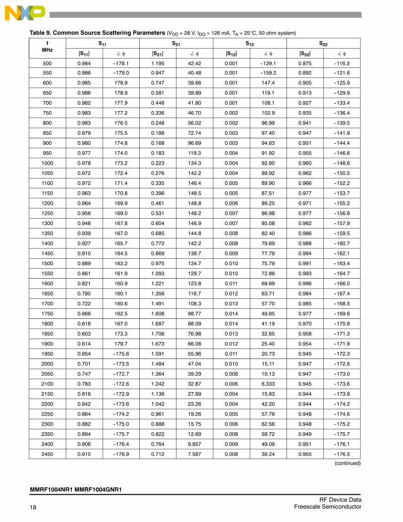
Table 9. Common Source Scattering Parameters (VDD = 28 V, IDQ = 126 mA, TA = 25C, 50 ohm system)
fMHz
S11 S21 S12 S22
|S11| |S21| |S12| |S22|
500 0.984 --178.1 1.195 42.42 0.001 --129.1 0.875 --116.3
550 0.986 --179.0 0.947 40.48 0.001 --159.2 0.892 --121.6
600 0.985 179.9 0.747 39.66 0.001 147.4 0.905 --125.9
650 0.986 178.9 0.581 39.89 0.001 119.1 0.913 --129.9
700 0.982 177.9 0.446 41.80 0.001 108.1 0.927 --133.4
750 0.983 177.2 0.336 46.70 0.002 102.9 0.935 --136.4
800 0.983 176.5 0.248 56.02 0.002 96.99 0.941 --139.5
850 0.979 175.5 0.188 72.74 0.003 97.40 0.947 --141.9
900 0.980 174.8 0.168 96.69 0.003 94.63 0.951 --144.4
950 0.977 174.0 0.183 119.3 0.004 91.92 0.955 --146.6
1000 0.978 173.2 0.223 134.3 0.004 92.80 0.960 --148.6
1050 0.972 172.4 0.276 142.2 0.004 89.92 0.962 --150.5
1100 0.972 171.4 0.335 146.4 0.005 89.90 0.966 --152.2
1150 0.963 170.8 0.396 148.5 0.005 87.51 0.977 --153.7
1200 0.964 169.9 0.461 148.8 0.006 89.25 0.971 --155.2
1250 0.956 169.0 0.531 148.2 0.007 86.98 0.977 --156.8
1300 0.948 167.8 0.604 146.9 0.007 85.08 0.982 --157.9
1350 0.939 167.0 0.685 144.8 0.008 82.40 0.986 --159.5
1400 0.927 165.7 0.772 142.2 0.008 79.69 0.988 --160.7
1450 0.910 164.5 0.869 138.7 0.009 77.79 0.994 --162.1
1500 0.889 163.2 0.975 134.7 0.010 75.79 0.991 --163.4
1550 0.861 161.9 1.093 129.7 0.010 72.86 0.993 --164.7
1600 0.821 160.9 1.221 123.8 0.011 69.89 0.996 --166.0
1650 0.780 160.1 1.356 116.7 0.012 63.71 0.984 --167.4
1700 0.722 160.6 1.491 108.3 0.013 57.70 0.985 --168.5
1750 0.666 162.5 1.606 98.77 0.014 49.85 0.977 --169.6
1800 0.618 167.0 1.687 88.09 0.014 41.19 0.970 --170.8
1850 0.603 173.3 1.706 76.98 0.013 32.65 0.958 --171.3
1900 0.614 179.7 1.673 66.08 0.012 25.40 0.954 --171.9
1950 0.654 --175.6 1.591 55.96 0.011 20.73 0.945 --172.3
2000 0.701 --173.5 1.484 47.04 0.010 15.11 0.947 --172.6
2050 0.747 --172.7 1.364 39.29 0.008 10.13 0.947 --173.0
2100 0.783 --172.6 1.242 32.87 0.006 6.333 0.945 --173.6
2150 0.816 --172.9 1.136 27.69 0.004 15.63 0.944 --173.9
2200 0.842 --173.6 1.042 23.26 0.004 42.20 0.944 --174.2
2250 0.864 --174.2 0.961 19.26 0.005 57.76 0.948 --174.6
2300 0.882 --175.0 0.888 15.75 0.006 62.56 0.948 --175.2
2350 0.894 --175.7 0.822 12.69 0.008 59.72 0.949 --175.7
2400 0.906 --176.4 0.764 9.857 0.009 49.09 0.951 --176.1
2450 0.910 --176.9 0.712 7.587 0.008 39.24 0.955 --176.5
(continued)

MMRF1004NR1 MMRF1004GNR1
19RF Device DataFreescale Semiconductor
Table 9. Common Source Scattering Parameters (VDD = 28 V, IDQ = 126 mA, TA = 25C, 50 ohm system) (continued)
fMHz
S11 S21 S12 S22
|S11| |S21| |S12| |S22|
2500 0.923 --177.5 0.666 5.462 0.006 42.56 0.957 --177.2
2550 0.927 --178.0 0.625 3.680 0.006 52.25 0.962 --177.8
2600 0.937 --178.8 0.591 1.864 0.006 60.26 0.961 --178.4
2650 0.937 --179.0 0.559 0.237 0.007 64.14 0.964 --179.1
2700 0.942 --179.8 0.529 --1.378 0.007 65.62 0.964 --179.6
2750 0.945 --179.9 0.504 --2.768 0.007 64.71 0.964 179.7
2800 0.946 179.5 0.479 --4.088 0.007 67.58 0.966 179.4
2850 0.950 179.3 0.456 --5.412 0.007 75.44 0.966 178.8
2900 0.949 178.8 0.436 --6.305 0.008 82.04 0.964 178.3
2950 0.952 178.5 0.419 --7.279 0.009 83.60 0.967 177.9
3000 0.950 178.4 0.402 --8.087 0.011 83.41 0.968 177.4
3050 0.958 177.9 0.387 --9.138 0.012 81.35 0.964 176.8
3100 0.953 177.7 0.373 --9.904 0.013 77.45 0.969 176.4
3150 0.957 177.2 0.362 --10.86 0.014 70.98 0.970 176.2
3200 0.960 177.4 0.350 --11.79 0.013 67.00 0.970 175.5

20RF Device Data
Freescale Semiconductor
MMRF1004NR1 MMRF1004GNR1
PACKAGE DIMENSIONS

MMRF1004NR1 MMRF1004GNR1
21RF Device DataFreescale Semiconductor

22RF Device Data
Freescale Semiconductor
MMRF1004NR1 MMRF1004GNR1

MMRF1004NR1 MMRF1004GNR1
23RF Device DataFreescale Semiconductor

24RF Device Data
Freescale Semiconductor
MMRF1004NR1 MMRF1004GNR1

MMRF1004NR1 MMRF1004GNR1
25RF Device DataFreescale Semiconductor

26RF Device Data
Freescale Semiconductor
MMRF1004NR1 MMRF1004GNR1
PRODUCT DOCUMENTATION
Refer to the following documents to aid your design process.
Application Notes AN1907: Solder Reflow Attach Method for High Power RF Devices in Plastic Packages
AN1955: Thermal Measurement Methodology of RF Power Amplifiers
AN3789: Clamping of High Power RF Transistors and RFICs in Over--Molded Plastic Packages
Engineering Bulletins EB212: Using Data Sheet Impedances for RF LDMOS Devices
REVISION HISTORY
The following table summarizes revisions to this document.
Revision Date Description
0 Dec. 2013 Initial Release of Data Sheet
1 Jan. 2014 Fig. 1, Pin Connections: corrected pin 1 and pin 2 labels to align with labelling in the mechanical outline, p. 1
Table 2. Thermal Characteristics: CW thermal value changed from 2.5 to 2.3C/W to reflect recent thermaltest results; two--tone test corrected from 5 W PEP to 10 W PEP and the thermal value changed from 5.9 to2.9C/W to reflect recent thermal test results, p. 2

MMRF1004NR1 MMRF1004GNR1
27RF Device DataFreescale Semiconductor
Information in this document is provided solely to enable system and softwareimplementers to use Freescale products. There are no express or implied copyrightlicenses granted hereunder to design or fabricate any integrated circuits based on theinformation in this document.
Freescale reserves the right to make changes without further notice to any productsherein. Freescale makes no warranty, representation, or guarantee regarding thesuitability of its products for any particular purpose, nor does Freescale assume anyliability arising out of the application or use of any product or circuit, and specificallydisclaims any and all liability, including without limitation consequential or incidentaldamages. “Typical” parameters that may be provided in Freescale data sheets and/orspecifications can and do vary in different applications, and actual performance mayvary over time. All operating parameters, including “typicals,” must be validated foreach customer application by customer’s technical experts. Freescale does not conveyany license under its patent rights nor the rights of others. Freescale sells productspursuant to standard terms and conditions of sale, which can be found at the followingaddress: freescale.com/SalesTermsandConditions.
Freescale and the Freescale logo are trademarks of Freescale Semiconductor, Inc.,Reg. U.S. Pat. & Tm. Off. All other product or service names are the property of theirrespective owners.E 2013--2014 Freescale Semiconductor, Inc.
How to Reach Us:
Home Page:freescale.com
Web Support:freescale.com/support
Document Number: MMRF1004NRev. 1, 1/2014