RF Amplifier Output Voltage, Current, Power and …6-201… · How much output voltage, current and...
6
64 hf-praxis 6/2017 RF & Wireless How much output voltage, current and power can RF amplifiers provide? This question is often asked by novice test engineers as well as seasoned RF professionals. Depending on the application, there is often an under- lying desire to maximize one of the three parameters: power, voltage or current. While one would think that a simple application of Ohm’s law is called for, this would only apply given ideal conditions, such as when an RF amplifier with a typical 50 Ω output resistance is driving a 50 Ω load. In this rare case where the load impedance perfectly matches the amplifier output impedance, the power delivered to the load is simply the rated power of the amplifier. There is absolutely no reflected power and thus, there is no need to limit or control the gain of the amplifier to protect it from excessive reflected power. Unfortunately, such ideal conditions rarely apply in actual “real world” applications. Real amplifiers are required to drive varying load impedances. The mismatch between these “real” loads and the amplifier’s out- put impedance result in a percentage of the forward power being reflected back to the amplifier. In some cases, excessive reflected power can damage an amplifier and precautions that may affect forward power are required. Given these realities, how does one go about determining output voltage, current and power? Again Ohm’s law comes to the rescue, but with the caveat that the actual power delivered to the load (net forward power after the application of any VSWR protection less reflected power) must be determined before applying Ohm’s law. This Application note will highlight some of the major RF amplifier characteri- stics that impact forward power as well as net power allowing the use of Ohm’s law, even when conditions are far from ideal. Back to Basics: Ohm’s Law Ohm’s law states that the amount of current flowing between two points in an electrical circuit is directly proportional to the voltage impressed across the two points and inver- sely proportion to the resistance between the points. Thus, the equation is the basic form of Ohm’s law where the current I is in units of amperes (A), the Electromotive Force (EMF) or difference of electrical potential E is in volts (V), and R is the circuit resistance given in ohms (Ω). Applying the standard equation rela- ting electrical power to voltage and current A cross multiplying and rearranging each of the variables results in the equations shown in the Ohm’s law pie chart (see Fig 1) sho- wing the various combinations of the four variables, I, V, Ω and W. Let’s use Ohm’s pie chart to determine the output voltage, current, and power of a 50 Ω amplifier ope- rating under ideal conditions. Example Assume we have a 100 watt amplifier with 50 Ω output impedance driving a 50 Ω load. This is an ideal situation in that 100% of the forward power will be absorbed in the load and therefore there is no reflected power in this example.The full 100 Watts will be delivered to the 50 Ω load. RF Amplifier Output Voltage, Current, Power and Impedance Relationship Figure 1: Ohm’s Law pie chart Application Note #49 Jason Smith, Manager Applications Engineer Pat Malloy, Sr. Applications Engineer rf/microwave instrumentation www.ar-worldwide.com
Transcript of RF Amplifier Output Voltage, Current, Power and …6-201… · How much output voltage, current and...

64 hf-praxis 6/2017
RF & Wireless
How much output voltage, current and power can RF amplifiers provide? This question is often asked by novice test engineers as well as seasoned RF professionals. Depending on the application, there is often an under-lying desire to maximize one of the three parameters: power, voltage or current. While one would think that a simple application of Ohm’s law is called for, this would only apply given ideal conditions, such as when an RF amplifier with a typical 50 Ω output resistance is driving a 50 Ω load. In this rare case where the load impedance perfectly matches the amplifier output impedance, the power delivered to the load is simply the rated power of the amplifier. There is absolutely no reflected power and thus, there is no need to limit or control the gain of the amplifier to protect it from excessive reflected power.
Unfortunately, such ideal conditions rarely apply in actual “real world” applications. Real amplifiers are required to drive varying load impedances. The mismatch between these “real” loads and the amplifier’s out-
put impedance result in a percentage of the forward power being reflected back to the amplifier. In some cases, excessive reflected power can damage an amplifier and precautions that may affect forward power are required. Given these realities, how does one go about determining output voltage, current and power? Again Ohm’s law comes to the rescue, but with the caveat that the actual power delivered to the load (net forward power after the application of any VSWR protection less reflected power) must be determined before applying Ohm’s law. This Application note will highlight some of the major RF amplifier characteri-stics that impact forward power as well as net power allowing the use of Ohm’s law, even when conditions are far from ideal.
Back to Basics: Ohm’s Law
Ohm’s law states that the amount of current flowing between two points in an electrical circuit is directly proportional to the voltage impressed across the two points and inver-sely proportion to the resistance between the points. Thus, the equation
is the basic form of Ohm’s law where the current I is in units of amperes (A), the Electromotive Force (EMF) or difference of electrical potential E is in volts (V), and R is the circuit resistance given in ohms (Ω). Applying the standard equation rela-ting electrical power to voltage and current
A
cross multiplying and rearranging each of the variables results in the equations shown in the Ohm’s law pie chart (see Fig 1) sho-wing the various combinations of the four variables, I, V, Ω and W. Let’s use Ohm’s pie chart to determine the output voltage, current, and power of a 50 Ω amplifier ope-rating under ideal conditions.
Example
Assume we have a 100 watt amplifier with 50 Ω output impedance driving a 50 Ω load. This is an ideal situation in that 100% of the forward power will be absorbed in the load and therefore there is no reflected power in this example.The full 100 Watts will be delivered to the 50 Ω load.
RF Amplifier Output Voltage, Current, Power and Impedance Relationship
Figure 1: Ohm’s Law pie chart
Application Note #49 Jason Smith,
Manager Applications Engineer Pat Malloy, Sr. Applications Engineer
rf/microwave instrumentation www.ar-worldwide.com
hf-praxis 6/2017 65
RF & Wireless
Selecting appropriate formulas from the Ohm’s pie chart, one can easily characte-rize this ideal amplifier:
√ Substituting known values:
√ = 70,7 Vrms
Thus, the output voltage across the 50 Ω load is 70.7 Vrms
Substituting known values:
= 1,41 Arms
The output load current is 1,41 Arms
As can be seen from the above example, when impedances match, power, voltage, and current are easily determined by the application of Ohm’s law. Now let’s con-sider “real life” amplifiers and the effects they have on the determination of output voltage, current and power.
Impedance Mismatch: The danger of impedance mismatch and methods used to protect amplifiersMaximum power is transferred to the load only when the load impedance matches the amplifier’s output impedance. Unfortunately, this is rarely the case. In these “typical” situ-ations, reflections occur at the load and the difference between the forward power and that delivered to the load is reflected back to the amplifier. A voltage standing wave is created by the phase addition and subtrac-tion of the incident and reflected voltage waveforms. Power amplifiers must either be capable of absorbing this reflected power or they must employ some form of protection to prevent damage to the amplifier.For example, an open or short circuit placed on the 100 watt power amplifier discussed above would result in an infinite voltage standing wave ratio (VSWR). Since
for Z0 >ZL and
for ZL > Z0
it can be seen that VSWR is always ≥1. With no active VSWR protection, an open circuit at the load would result in a doubling of the output voltage to 141,4 Vrms, while a short circuit would increase the output current to 2,82 Arms. In either of these worst case sce-narios, the 100 watt power amplifier must
tolerate a maximum power of 200 watts (100 watts forward + 100 watts reverse).Clearly this is cause for concern and ampli-fier designers must deal with the very real possibility that the amplifier’s output might either be accidentally shorted or the load could be removed. Consequently, all ampli-fiers should employ some form of protection when VSWR approaches dangerous levels. The following is a partial list (most desirable to least desirable) of some methods used:
Overdesign• All Solid-state devices and power combi-
ners are conservatively designed to pro-vide sufficient ruggedness and heat dis-sipation to accommodate infinite VSWR.
• No additional active VSWR protection circuitry is required with this approach.
• This conservative approach is found on AR’s low to mid power amplifiers.
Active monitoring of VSWR resulting in a reduction in amplifier gain when VSWR approaches dangerous levels• When VSWR exceeds a safe level the for-
ward power is reduced. This technique is sometimes referred to as “gain fold-back” or just “fold-back”.
• AR’s high power solid-state amplifiers will fold-back when reflected power reaches 50% of the rated power corresponding to a VSWR of 6:1 and will withstand any amount of mismatch.
Active monitoring of VSWR leading to a shut down when VSWR exceeds a safe level• This is considered a brute-force tech-
nique that can lead to undesirable test disruptions.
• AR does not use this technique in any of its amplifiers.
Active thermal monitoring• High VSWR will cause a buildup of
heat. When a predetermined tempera-ture threshold is exceeded, the amplifier is shut down.
• Due to the nature of thermal time con-stants, this approach is relatively slow. Extreme variations in VSWR may not immediately result in shut down.
• AR amplifiers employ some degree of ther-mal monitoring for circuit protection but do not rely on this relatively slow method to protect against extreme VSWR.
Active monitoring of both output voltage and/or current• Limits are set for both voltage and/or cur-
rent similar to restrictions placed on DC power supplies.
• If either of the two parameters is excee-ded, the amplifier is shut down.
Many amplifiers are designed with little or no concern regarding load mismatch. It is assumed that the application involves a load that matches that of the amplifier. In appli-cations like electromagnetic compatibility (EMC) immunity testing where impedance mismatch is the norm, care must be taken in selecting an amplifier that can tolerate any mismatch while still delivering the required power.
AR solid-state amplifiers have been de-signed to tolerate extreme load mismatch. They are exceptionally rugged and provide superior protection while delivering maxi-mum output power to any load. Impedance mismatch is discussed in further detail in Application Note #27A, “Importance of Mismatch Tolerance for Amplifiers Used in Susceptibility Testing”.
What will be the effect of VSWR protection on forward power, or power available to the load?Let’s first look at the various methods used to protect AR amplifiers from the ill effects of extreme VSWR.
• Class A amplifiers designed to tolerate infinite VSWR: This type of amplifier will not fold-back or shut off when ope-rating into a high VSWR. (Most AR low to medium power amplifiers fit in this category.)
• With these amplifiers, the forward power is always the rated power, and is indepen-dent of load
• Example: A 100 watt amplifier will pro-vide 100 watts forward power irrespec-tive of load variations
• Fold-back based on reflected power: This technique is used for high power AR amplifiers where the reflected power is not allowed to exceed 50% of the rated power.
• These larger amplifiers provide full rated power to the load for any VSWR up to 6:1. As VSWR increases beyond this level, fold-back is used to limit the reflected power to no more than 50% of the rated power, regardless of load variations.
• In this case, available forward power is equal to the rated power until a VSWR of 6:1 is reached. At this point, 50% of
66 hf-praxis 6/2017
RF & Wireless
the forward power is reflected. For any VSWR greater than 6:1, the forward power is reduced sufficiently to insure that the reverse power never exceeds 50% of the rated power.
• Example: A 1000 watt amplifier will limit forward power to 50% of the rated power for any load mismatch greater than 6:1. Thus, since 500 watts is the maximum amount of reflected power, the forward power is 1000 watts for VSWR 6:1 and somewhere between 1000 and 500 watts for VSWR ≥ 6:1.
• Voltage and current limitedFor a Voltage/Current limited amplifier, calculations are much simpler. Ohm’s law can be directly applied to find net power, voltage, and load current.The amplifier output impedance is:
For load impedance higher than the ampli-fier output impedance the amplifier is pro-tected by the voltage limit. Regardless of the load impedance the output voltage is clamped near the specified minimum vol-tage rating. Applying ohm’s law:
and
For load impedances lower than the ampli-fier output impedance the amplifier is pro-tected by the current limit. Regardless of how small the load is, the output current will not exceed a value near the specified minimum current rating. Again applying ohm’s law:
= x Ω and
The following comments apply to amplifiers that don’t use one of the AR style VSWR protection methods listed above:
• Amplifiers that protect by shutting down or turning off the RF output:
• Forward power will be 0 if VSWR is excessive. This may occur at a VSWR as low as 2:1, but more often occurs for a VSWR somewhere between 2:1 and 3:1.
Clearly, amplifiers that either don’t employ VSWR protection or use this brute force VSWR scheme cannot be used in applica-
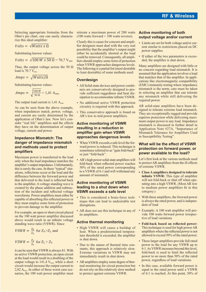
Figure 2: Power vs. Load Impedance 75A400
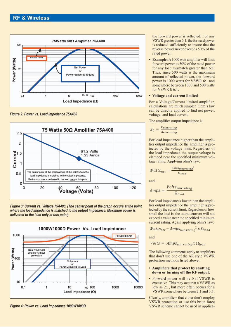
Figure 3: Current vs. Voltage 75A400. (The center point of the graph occurs at the point where the load impedance is matched to the output impedance. Maximum power is delivered to the load only at this point)
Figure 4: Power vs. Load Impedance 1000W1000D

hf-praxis 6/2017 67
RF & Wireless
tions where load mismatches are expected. Amplifiers that employ fold-back schemes at even lower VSWR levels than noted above are also in this category and are unsuitable for applications characterized by high load VSWR such as EMC immunity testing and research applications where load impedance is unknown.
Output power loss due to load mismatchWe have concentrated on the topic of forward power up to this point. This is the power actu-ally available at the load. Jacobi’s Law, also known as the “maximum power theorem” states that “Maximum power is transferred when the internal resistance of the source equals the resistance of the load, when the external resistance can be varied, and the internal resistance is constant.” This effect is clearly observed when load impedance differs (greater or less) from the amplifier’s output impedance. As VSWR increases, an ever greater portion of the forward power is reflected back to the amplifier. Since net power is calculated by subtracting the reflected power from the forward power, it is apparent that any VSWR other than 1:1 will reduce the actual power absorbed by the load. The amount of power delivered to the load can be calculated using the follow-ing standard RF formulas:Reflection Coefficient:
The two impedances are the load impedance and the output impedance of the amplifier.Once the forward power has been deter-mined and the reflection coefficient calcu-lated, the net power delivered to the load is found by merely substituting values into the following equation:
Furthermore, given the net power and load impedance one can then calculate the out-put current and voltage using Ohms law.
Real ExamplesNow that we have investigated the nuances involved in determining output power, vol-tage and current of RF power amplifiers in general, let’s look at four existing AR ampli-fiers and how they deal with load mismatch.Example 1: Most low and medium power amplifiers are of the Class A design and have nominal 50 Ω output impedance. A typical amplifier of this type is the 75A400 power amplifier:
• 10 kHz – 400 MHz bandwidth
• 75 Watts minimum RF output
• No active protection is required given its very robust, conservative design
• Full forward power is provided into any load impedance
Figure 2 clearly demonstrates the best pos-sible scenario provided by the 75A400. The forward power is constant at 75 watts irrespective of load impedance. The center point of the graph demonstrates maximum power transfer per Jacobi’s Law where the 50 Ω amplifier is driving a 50 Ω load and the blue output power curve clearly demonstrates the reduction in net power per the maximum power theorem as the load varies from the ideal of 50 Ω. Note that even though 75 watts is available independent of the load impedance (orange curve), there is
only one point where the power delivered to the load is equal to the forward power; the point where the load impedance mat-ches the amplifiers output impedance. The fall-off of the power delivered to the load on either side of the 50 Ω load impedance is the result of load VSWR causing an ever increasing portion of the forward power to be reflected back to the amplifier. Recall that Pnet = Pfwd - Pref. Figure 3 plots the voltage and current over the entire range of load impedance. The center point represents the voltage and cur-rent produced when the load impedance matches the amplifiers 50 Ω output impe-dance. Loads greater than 50 Ω are plotted to the right of the center point and loads less than 50 Ω appear to the left. The end points demonstrate the two possibilities of a worst case mismatch; an open where the output
Figure 5: Current vs. Voltage 1000W1000D
Figure 6: Power vs. Load Impedance 800A3A
68 hf-praxis 6/2017
RF & Wireless
voltage is at a maximum with zero current, and a short where the current is maximum with zero voltage.
The graphs in figure 2 and 3 are based on the minimum rated output of the amplifier across its entire operating frequency range. There most likely will be spots within the frequency range where the output power will exceed the specified minimum rated output power. To avoid unexpected results, always request a copy of specific production test data before placing an amplifier in service.
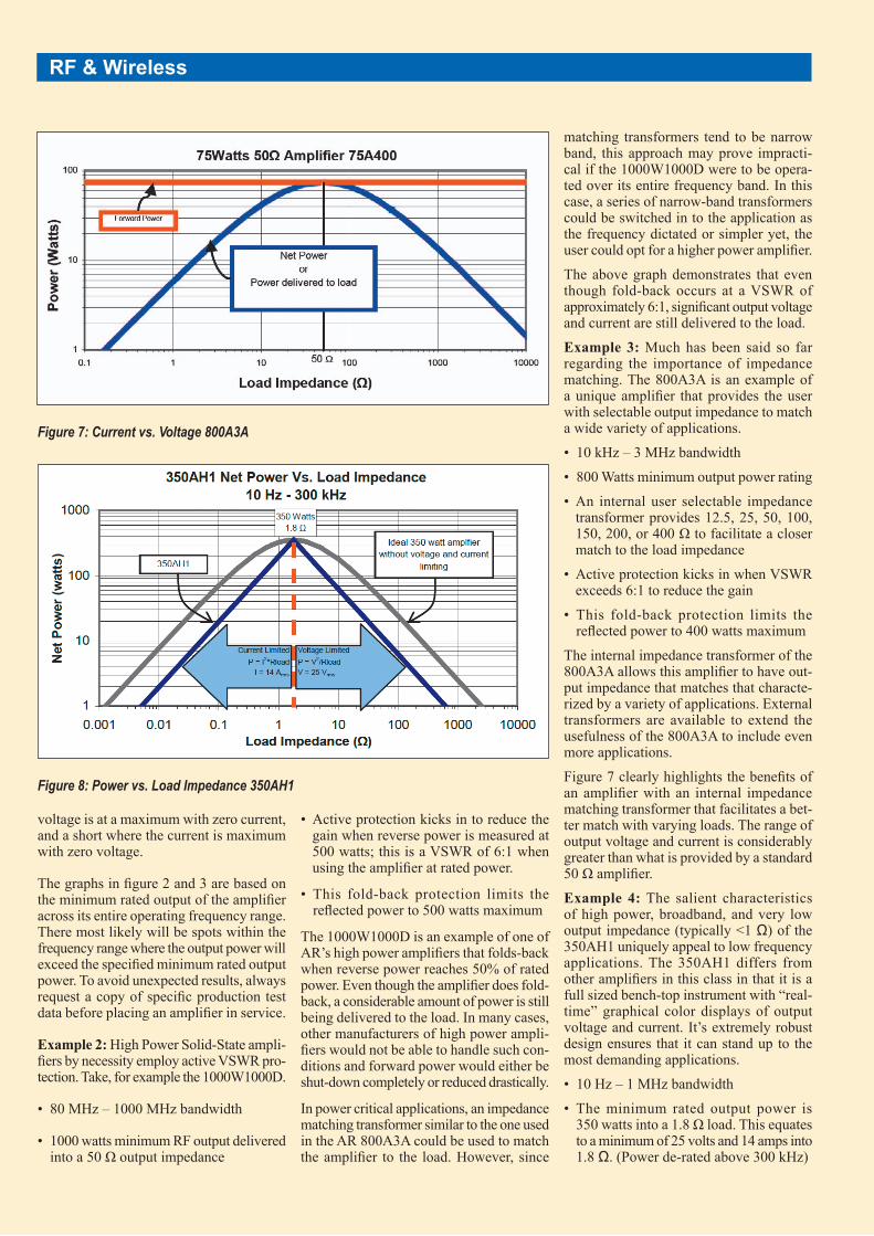
Example 2: High Power Solid-State ampli-fiers by necessity employ active VSWR pro-tection. Take, for example the 1000W1000D.
• 80 MHz – 1000 MHz bandwidth
• 1000 watts minimum RF output delivered into a 50 Ω output impedance
• Active protection kicks in to reduce the gain when reverse power is measured at 500 watts; this is a VSWR of 6:1 when using the amplifier at rated power.
• This fold-back protection limits the reflected power to 500 watts maximum
The 1000W1000D is an example of one of AR’s high power amplifiers that folds-back when reverse power reaches 50% of rated power. Even though the amplifier does fold-back, a considerable amount of power is still being delivered to the load. In many cases, other manufacturers of high power ampli-fiers would not be able to handle such con-ditions and forward power would either be shut-down completely or reduced drastically.
In power critical applications, an impedance matching transformer similar to the one used in the AR 800A3A could be used to match the amplifier to the load. However, since
matching transformers tend to be narrow band, this approach may prove impracti-cal if the 1000W1000D were to be opera-ted over its entire frequency band. In this case, a series of narrow-band transformers could be switched in to the application as the frequency dictated or simpler yet, the user could opt for a higher power amplifier.
The above graph demonstrates that even though fold-back occurs at a VSWR of approximately 6:1, significant output voltage and current are still delivered to the load.
Example 3: Much has been said so far regarding the importance of impedance matching. The 800A3A is an example of a unique amplifier that provides the user with selectable output impedance to match a wide variety of applications.
• 10 kHz – 3 MHz bandwidth
• 800 Watts minimum output power rating
• An internal user selectable impedance transformer provides 12.5, 25, 50, 100, 150, 200, or 400 Ω to facilitate a closer match to the load impedance
• Active protection kicks in when VSWR exceeds 6:1 to reduce the gain
• This fold-back protection limits the reflected power to 400 watts maximum
The internal impedance transformer of the 800A3A allows this amplifier to have out-put impedance that matches that characte-rized by a variety of applications. External transformers are available to extend the usefulness of the 800A3A to include even more applications.
Figure 7 clearly highlights the benefits of an amplifier with an internal impedance matching transformer that facilitates a bet-ter match with varying loads. The range of output voltage and current is considerably greater than what is provided by a standard 50 Ω amplifier.
Example 4: The salient characteristics of high power, broadband, and very low output impedance (typically <1 Ω) of the 350AH1 uniquely appeal to low frequency applications. The 350AH1 differs from other amplifiers in this class in that it is a full sized bench-top instrument with “real-time” graphical color displays of output voltage and current. It’s extremely robust design ensures that it can stand up to the most demanding applications.
• 10 Hz – 1 MHz bandwidth
• The minimum rated output power is 350 watts into a 1.8 Ω load. This equates to a minimum of 25 volts and 14 amps into 1.8 Ω. (Power de-rated above 300 kHz)
Figure 7: Current vs. Voltage 800A3A
Figure 8: Power vs. Load Impedance 350AH1

hf-praxis 6/2017 69
RF & Wireless
• Source impedance is rated at <1 Ω (Since the output voltage and current are speci-fied, output impedance is not used in the forward power calculations.)
• Effective source impedance is 1.8 Ω (Zo=Vo/Io= 25 V/14 A)
• Output protection limits both the voltage and current at rated values into any load. For loads less than 1.8 Ω, the output cur-rent is limited. For loads exceeding 1.8 Ω the output voltage is limited.
This is an example of an amplifier with a 1.8 Ω effective output impedance. Due to the voltage and current limiting protection of the amplifier, VSWR does not play a role in lost power delivered to the load.
Figure 9 plots the available output voltage and current from the 350AH1. The gray area is provided to indicate a more “typical” out-put profile. Individual amplifier characteri-stics will vary and are somewhat influenced by operating frequency and system losses.
SummaryThe age old question of “How much out-put voltage, current, and power can I expect
from my amplifier?” can in rare cases be answered by merely applying Ohm’s law assuming the net power or power delivered to the load is simply the rated power out-put of the amplifier. In most cases, practical issues such as VSWR and forward power concerns must be considered before app-lying Ohm’s law. While this application
note has provided guidance in this matter, AR firmly believes that the best approach is to apply actual test data when calculating output parameters. If you are the least bit uncomfortable with this exercise, feel free to contact one of our Application Engineers. We would be more than happy to guide you through the process. ◄
Figure 9: Current vs. Voltage 350AH1
To coincide with Space Tech Expo, taking place in Pasadena, California, USA over May 23 to 25, Knowles Capacitors has produced a new shortform capability guide outlining their range of Space Heritage pro-ducts. This user friendly guide provides an overview of Knowles’ space heritage and involvement in space grade platforms, as well as illustrating the specialty High REL and approved parts that find use in critical or high reliability environments.
Knowles brands Syfer Technology and Novacap have drawn on the experience and expertise gained on numerous platforms to remain a leading supplier of Multilayer Ceramic Capacitors (MLCC) and assem-blies for military and commercial space programs. The products detailed in the guide include EMI filters, High Rel and High Temperature Capacitors and Space Grade ranges including leaded & capaci-tor assembly options.
Of particular interest, and on show on booth 2024 at Space Tech, is the catalog range of Single Layer Capacitor (SLC) Filters, Power Dividers and Directional Couplers from Knowles brand DLI. The filter series encapsulates SM Bandpass, Lowpass, Highpass and Cavity Filters,
finding typical applications in Microwave Radar, Satellite & Radio Comms, Test Equipment and 5G Base Stations amongst others. These SMD products are designed to work at up to 42 GHz; with temperature stability over -55 to +125 °C: power hand-
ling up to 40 Watts and high repeatability thanks to their precision thin film fabrica-tion. The range is also EAR99 approved.
■ Knowles (UK) Ltd. www.knowlescapacitors.com
News