Optical properties of silicon nitride films deposited by ...
ECS Journal of Solid State Science and Technology, 6 (10) P691-P714 (2017) P691
Review—Silicon Nitride and Silicon Nitride-Rich Thin FilmTechnologies: Trends in Deposition Techniques and RelatedApplicationsAlain E. Kaloyeros,a Fernando A. Jove,b Jonathan Goff,b and Barry Arklesb,∗,z
aSUNY Polytechnic Institute, Albany, New York 12203, USAbGelest, Inc., Morrisville, Pennsylvania 19067, USA
This article provides an overview of the state-of-the-art chemistry and processing technologies for silicon nitride and silicon nitride-rich films, i.e., silicon nitride with C inclusion, both in hydrogenated (SiNx:H and SiNx:H(C)) and non-hydrogenated (SiNx andSiNx(C)) forms. The emphasis is on emerging trends and innovations in these SiNx material system technologies, with focus on Siand N source chemistries and thin film growth processes, including their primary effects on resulting film properties. It also illustratesthat SiNx and its SiNx(C) derivative are the focus of an ever-growing research and manufacturing interest and that their potentialusages are expanding into new technological areas.© The Author(s) 2017. Published by ECS. This is an open access article distributed under the terms of the Creative CommonsAttribution 4.0 License (CC BY, http://creativecommons.org/licenses/by/4.0/), which permits unrestricted reuse of the work in anymedium, provided the original work is properly cited. [DOI: 10.1149/2.0011710jss] All rights reserved.
Manuscript submitted June 28, 2017; revised manuscript received September 5, 2017. Published September 29, 2017.
Silicon nitride and carbide thin films, primarily in the form of sil-icon nitride (SiNx), silicon carbide (SiCy), and silicon carbo-nitride(SiNxCy), where 0 < x < 1.33 and 0 < y < 1, are experiencing a bur-geoning of research interest across multiple application sectors. Theappeal of these Si-based coatings is attributed to their highly desirablecombination of physical, mechanical, electrical, and optoelectronicproperties making them prime candidates for applications in the auto-motive, aerospace, computer chip, solar, light-emitting, and medicalindustries.1–6 In consideration of the intense current interest in SiNx
and SiNxCy, and the expectation that their applications will continue towitness further expansion and extensive diversification, we present anoverview on the latest trends and developments in hydrogenated andnon-hydrogenated silicon nitride and silicon carbonitride depositiontechniques and associated post-deposition processing technologies.Given the fast-moving nature of SiNx and SiNxCy technological ad-vances, the intent is to present an survey of work published withinthe last five years for silicon nitride and silicon nitride-rich films, i.e.,silicon nitride with C inclusion, both in hydrogenated (SiNx:H andSiNx:H(C)) and non-hydrogenated (SiNx and SiNx(C)) forms. Prioryears reports will be discussed only in the context of providing ap-propriate background and support for the more contemporary resultssummarized herein. This article is not intended to be a comprehen-sive review, but instead is meant to provide the reader with a focusedanalysis of research directions particularly where, in the authors’ ex-perience, they are reflective of potential commercial relevance.
The silicon nitride literature presents a complex picture of its prop-erties: mechanical, thermal, electrical, tribological, etc. In the bestcases, the properties are associated with well-defined chemical com-positions and morphologies. However, silicon nitride is frequentlydescribed by the process by which it is formed, and reported proper-ties are for compositions that are not fully defined. Accordingly, thisreview is centered on silicon nitride deposition and the processes andselected properties associated with specific modifications in deposi-tion techniques. While a detailed analysis of film physical, chemical,electrical and optical properties over the range of deposition tech-nologies and conditions is not presented herein, salient propertiesare summarized in tabular form. Analyses of thin film properties asfunction of most researched deposition techniques, and an evaluationof resulting applications as they pertain to film properties, will bepresented in a subsequent review.
For instance, SiNx, SiCy, and SiNxCy1–4 are employed as hard
protective coatings under challenging thermal, environmental, andchemical conditions due to their high hardness (potentially in ex-
∗Electrochemical Society Member.zE-mail: [email protected]
cess of 40GPa), effective oxidation resistance, elevated temperatureand thermal shock resistance as well as chemical stability, and attrac-tive mechanical, tribological and dielectric properties.5–9 In particular,bonding in SiNx, SiCy, and SiNxCy exhibits substantially greater cova-lent character than in silicon dioxide (SiO2). SiNx, SiCy, and SiNxCy
can therefore provide an intrinsically greater resistance to diffusivemigration than SiO2, a feature that is of utmost impact at nanoscaledimensions.
Ultrathin films of SiNx and SiCy are utilized in a broad spectrum ofapplications in integrated circuitry (IC) technologies, particularly inthe microprocessor unit (MPU), system-on-a-chip (SoC), flash mem-ory, and the vertical stacking of electronic devices in what is com-monly referred to as three-dimensional (3D) integrated systems.10 Forone, SiNx is widely adopted as diffusion barrier for silicon dioxide(SiO2) dielectric with the introduction of copper metallization struc-tures. Additionally, SiCy, SiNxCy, and SiCyOz are applied as diffusionbarriers in combination with low dielectric constant (κ) material re-placements to SiO2.11–13 Similarly, SiNx and SiNxCy are used as cap-ping layers and etch stops for copper interconnects either individuallyor, more recently, in combination with selective cobalt capping.14 Thedominant low interlevel dielectric (ILD) film for the bottom few metallayers of the MPU is SiOCH, and for flash memory architectures it isSiOC.10 Other IC applications incorporate SiNx as a dielectric such asmetal-insulator-metal capacitors and thin film transistors (TFTs) dueto its high dielectric constant which enables the deposition of thinnerfilms while preserving higher breakdown voltage and lower leakagecurrent.15,16
In an analogous manner, SiNx and SiCy thin films are success-fully incorporated into active optical and optoelectronic devices dueto their wide bandgap (2.3 eV for SiCy and 5.1 eV for SiNx), and el-evated electrical breakdown voltage, including panel displays, light-ing, and light-emitting devices.4,17–19 In this respect, both types ofSi-based coatings are employed as permeation barriers and encap-sulation layers in light-emitting devices (LEDs), and organic LEDs(OLEDs),20–23 as well as in the fabrication of various planar op-tical systems and optical waveguides.24 Additionally, SiNxCy andSiNx coatings are used or suggested as passivation layers in flexibleelectroluminescent devices.25,26 It should also be noted that amor-phous hydrogenated SiCxOz thin films are the subject of intenseexploration as potential candidates for optoelectronic devices, dueto their appealing photoluminescence characteristics. These includeboth white emission as well as emission in the blue at the highlydesirable 1540 nm optical wavelength, when doped with erbium(Er).27–30 Nitrogen-rich silicon and SiNx films also serve as host matrixfor Si nanocrystals for use in optoelectronic device applications.31,32
Other applications include the use of hydrogenated amorphous silicon-nitrogen (a-SiNx:H) films as an insulating layer in thin-film transistors
) unless CC License in place (see abstract). ecsdl.org/site/terms_use address. Redistribution subject to ECS terms of use (see 69.139.80.173Downloaded on 2017-10-08 to IP

P692 ECS Journal of Solid State Science and Technology, 6 (10) P691-P714 (2017)
(TFT) for liquid-crystal display (LCD) and other emerging displaysystems.15,16,33,34
The application of SiNx, SiCy, and SiNxCy also extends into thegreen energy field,15,16 primarily in solar cell applications. For exam-ple, microcrystalline and amorphous SiCy coatings are employed aswindow layers in thin film solar cells.35 And much like the case ofthe hard coatings and computer chip industries, SiNx and SiCy thinfilms are applied as passivation layers in silicon solar cells.36,37 Otherapplications include the use of Si-rich SiNx as host matrix for Sinanocrystals and Si nanoscale inclusions (Si-ni) light emitters for so-lar cell applications.31,38 Likewise, SiNx is witnessing extensive use inbiotechnology and medical fields, especially in medical devices due toits high chemical stability, enhanced wear endurance, improved frac-ture toughness, and, unlike its carbide analog, elevated thermal shockresistance, and good biocompatibility.39 The resulting functions in-clude usages in medical devices similar to the applications describedabove for IC systems.
In addition, SiNx can be employed as a protective coating in in vivoand in vitro environments, including, for example, viewing windowsfor medical devices, insulating membranes for cell electroporation,as well as in biosensors for a variety of health-related applications.40
In vivo studies demonstrate that SiNx can be considered biostable,although differences in bio-dissolution rates have been observed infilms prepared by different deposition techniques.32,41–43 The SiNx
materials are non-irritating. and are considered non-cytotoxic.44 Fur-thermore, they are not substrates for bacterial colonization and do notinhibit osteogenesis.45
It is also worth noting that the mechanical, optical, and electroniccharacteristics of SiNx and SiCy can be tightly controlled and sys-tematically customized as a function of carbon (C) and nitrogen (N)concentrations.46,47 This feature makes the SiNxCy phase a prime can-didate for applications which require micro-modulation of the SiNxCy
system to enable adjustable properties, such as those requiring tunableoptical bandgaps and refractive indicies. In particular, SiNxCy filmswere grown with a tunable bandgap in the range of 2.3eV to 5.0eV,depending on their C and N content.48,49
However, in most cases, the incorporation of other elements, par-ticularly hydrogen, is not accounted for. It is more proper to desig-nate amorphous hydrogenated silicon nitride as a-SiNx:H. Not onlydoes the amount of hydrogen incorporation affect physical, opti-cal, and dielectric properties (in accordance with the Lorentz-Lorenzrelationship)50 in what is commonly referred to as SiNx:H, the natureof the Si-H versus N-H bonding also plays a significant role in tailor-ing the resulting film characteristics.46–49 Another influencing factoris the Pauling relative electronegativity of the Si, N, and H elements(namely, Si:1.90; N:3.04; H:2.20). Si-N and N-H bonds have relativelyhigh dipole moments, while Si-H bonds have relatively low dipole mo-ments. Thus, even if the atom % of film compositions prepared withdifferent precursors are identical, the resulting films may have differ-ent atom bonding arrangements and the dielectric properties of theresulting films will vary.
Fundamental Properties of Silicon Nitride
A review of the state of the art in silicon nitride processing tech-nologies must begin with a summary of the fundamental propertiesof known phases of silicon nitride. Unfortunately, the last fully com-prehensive review of silicon nitride both in monolithic (bulk) and thinfilm forms predates current film deposition technologies.51
At present, there is no up-to-date compendium of single referencedata that completely describes the properties of silicon nitride in all ofits’ forms and compositions. More recent articles have examined spe-cific aspects of silicon nitride technologies.52,53 In particular, the reportby Riley52 provides a historical review of the progress of the siliconnitride ceramic system, including its evolution into a variety of highgrade ceramic materials. Corresponding properties such as crystalstructure, lattice diffusion and defect chemistry, oxidation, productionand general properties were assessed in detail. The work also surveyed
the development of microstructure-properties functionality relation-ships. Also, the review by Hampshire53 presented a survey of siliconnitride ceramics structure, processing, and properties, including mi-crostructural development, sialons, and applications. Newer reviewarticles of silicon nitride thin film deposition techniques are discussedin Overview of silicon nitride formation and deposition techniquessection.
Silicon nitride with the nominal stoichiometry Si3N4 (c-Si3N4) oc-curs in three crystalline forms: α, β, and γ, while amorphous SiNx
(a-SiNx) exists in various forms that display a range of physical,chemical, electrical, and mechanical properties. Additionally, the lit-erature generally refers to crystalline and amorphous silicon nitridewith different ratios of silicon to nitrogen as silicon nitride (namely,a-SiNx, or c-SiNx with 0 < x < 1.33), although a few reports describedsignificantly higher N/Si ratio.25
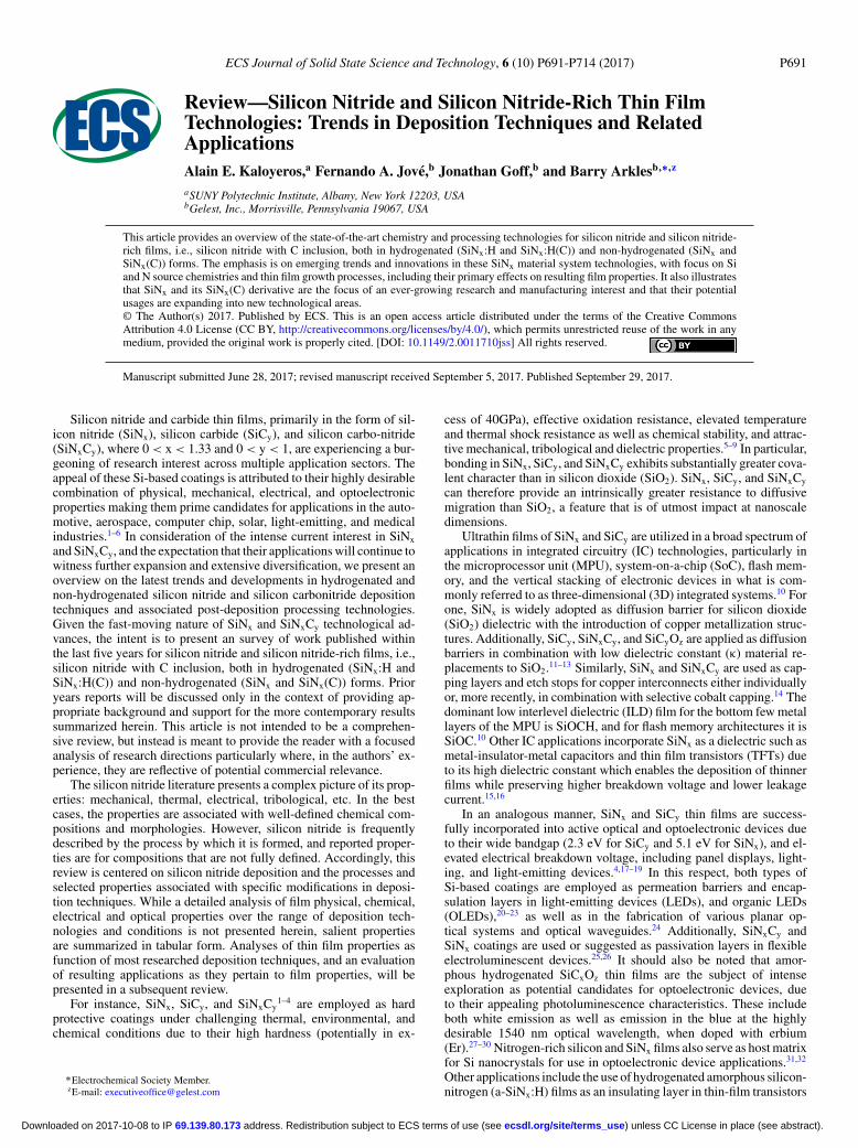
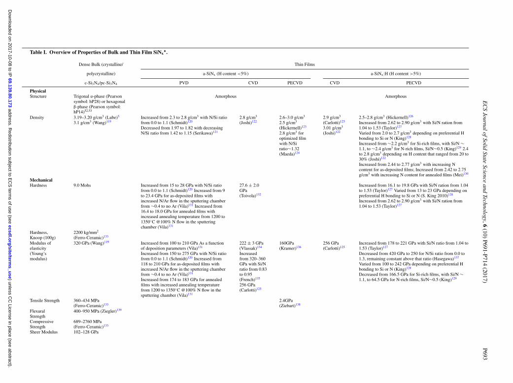
Table I presents nominal properties for silicon nitride. The datacompilation should be considered as a guide by the reader for bulkor crystalline (c-SiNx), polycrystalline (pc-SiNx), amorphous non-hydrogenated (a-SiNx) and hydrogenated (a- SiNx:H) thin films. Thedata is intended to represent salient, but not absolute, properties of thevarious forms of SiNx as determined at temperatures in the range of20◦–100◦C, except for self-evident thermal properties. In this context,the data should provide a baseline in the review and analysis of theproperties of SiNx films as reported in the published work.
Overview of Silicon Nitride Formation andDeposition Techniques
In general, silicon nitride monolithic (bulk) and film structures canbe prepared by: (1) solid phase synthesis (e.g., nitriding of Si, hotisostatic pressing of silicon nitride particles); (2) liquid phase synthe-sis (porous composite infiltration with thermal conversion or spin-ondeposition with thermal conversion from liquid or polymeric precur-sors); and (3) vapor phase synthesis in primarily thin and ultrathinfilms.
Silicon nitride monolithic (bulk) growth methodologies.—Solidphase synthesis of silicon nitride is usually associated with structuralceramic synthesis and the huge literature in this area is often asso-ciated with aerospace and military applications,53,54 but recently thetechnique has been extended to semiconductor substrates.55
Liquid phase synthesis, although it straddles application areas, isthe least studied of the processes and less is known about the result-ing film or bulk properties. Liquid phase synthesis, including spin-onand sol-gel techniques, is usually associated with linear (thermoplas-tic) polymers or crosslinked (thermoset) resins with alternating sili-con and nitrogen atoms in their backbone, and are broadly denotedpolysilazanes and aminosilanes.56–60 Early work in this area was di-rected toward thermolytic or pyrolytic conversion of polysilazanesdirectly into shaped or structural silicon nitride ceramics.61 The suc-cessful production of structural ceramics from liquid phase synthesishas not been achieved to date due to issues associated with ceramicyield, by-product diffusion, phase composition, density and chemicalcomposition.
In terms of chemical composition one of the two major classesof polysilazanes, organopolysilazanes (structure 1), has organic car-bon substitutions on the backbone leading in general to siliconcarbonitrides.62 Inorganic polysilazanes, alternately termed perhydri-dopolysilazanes (structure 2), lead more directly to silicon nitridestructures, but the polymers themselves are apt to have stability issuesthat lead to variability in performance.
1 2
NSi
CH3
HCH3
mNSi
H
H
H
m
) unless CC License in place (see abstract). ecsdl.org/site/terms_use address. Redistribution subject to ECS terms of use (see 69.139.80.173Downloaded on 2017-10-08 to IP
EC
SJournalofSolid
StateScience
andTechnology,6
(10)P691-P714
(2017)P693
Table I. Overview of Properties of Bulk and Thin Film SiNx∗.
Dense Bulk (crystalline/ Thin Films
polycrystalline) a-SiNx (H content <5%) a-SiNx:H (H content >5%)
c-Si3N4/pc-Si3N4 PVD CVD PECVD CVD PECVD
PhysicalStructure Trigonal α-phase (Pearson
symbol: hP28) or hexagonalβ-phase (Pearson symbol:hP14)52,53
Amorphous Amorphous
Density 3.19–3.20 g/cm3 (Lube)5
3.1 g/cm3 (Wang)119Increased from 2.3 to 2.8 g/cm3 with N/Si ratiofrom 0.0 to 1.1 (Schmidt)120
Decreased from 1.97 to 1.82 with decreasingN/Si ratio from 1.42 to 1.15 (Serikawa)121
2.8 g/cm3
(Joshi)1222.6–3.0 g/cm3
2.5 g/cm3
(Hickernell)123
2.8 g/cm3 foroptimized filmwith N/Siratio∼1.32(Maeda)124
2.9 g/cm3
(Carlotti)125
3.01 g/cm3
(Joshi)122
2.5–2.8 g/cm3 (Hickernell)126
Increased from 2.62 to 2.90 g/cm3 with Si/N ration from1.04 to 1.53 (Taylor)127
Varied from 2.0 to 2.7 g/cm3 depending on preferential Hbonding to Si or N (King)128
Increased from ∼2.2 g/cm3 for Si-rich films, with Si/N ∼1.1, to ∼2.4 g/cm3 for N-rich films, Si/N∼0.5 (King)129 2.4to 2.8 g/cm3 depending on H content that ranged from 20 to30% (Joshi)122
Increased from 2.44 to 2.77 g/cm3 with increasing Ncontent for as-deposited films; Increased from 2.42 to 2.75g/cm3 with increasing N content for annealed films (Mei)130
MechanicalHardness 9.0 Mohs Increased from 15 to 28 GPa with N/Si ratio
from 0.0 to 1.1 (Schmidt)120 Increased from 9to 23.4 GPa for as-deposited films withincreased N/Ar flow in the sputtering chamberfrom ∼0.4 to no Ar (Vila)131 Increased from16.4 to 18.0 GPa for annealed films withincreased annealing temperature from 1200 to1350◦C @100% N flow in the sputteringchamber (Vila)131
27.6 ± 2.0GPa(Toivola)132
Increased from 16.1 to 19.8 GPa with Si/N ration from 1.04to 1.53 (Taylor)127 Varied from 13 to 23 GPa depending onpreferential H bonding to Si or N (S. King 2010)128
Increased from 2.62 to 2.90 g/cm3 with Si/N ration from1.04 to 1.53 (Taylor)127
Hardness,Knoop (100g)
2200 kg/mm2
(Ferro-Ceramic)133
Modulus ofelasticity(Young’smodulus)
320 GPa (Wang)119 Increased from 100 to 210 GPa As a functionof deposition parameters (Vila)131
Increased from 150 to 275 GPa with N/Si ratiofrom 0.0 to 1.1 (Schmidt)120 Increased from118 to 210 GPa for as-deposited films withincreased N/Ar flow in the sputtering chamberfrom ∼0.4 to no Ar (Vila)131
Increased from 174 to 183 GPa for annealedfilms with increased annealing temperaturefrom 1200 to 1350◦C @100% N flow in thesputtering chamber (Vila)131
222 ± 3 GPa(Vlassak)134
Increasedfrom 320–360GPa with Si/Nratio from 0.83to 0.95(French)135
256 GPa(Carlotti)125
160GPa(Kramer)136
256 GPa(Carlotti)125
Increased from 178 to 221 GPa with Si/N ratio from 1.04 to1.53 (Taylor)127
Decreased from 420 GPa to 250 for N/Si ratio from 0.0 to1.3, remaining constant above that ratio (Hasegawa)137
Varied from 100 to 242 GPa depending on preferential Hbonding to Si or N (King)128
Decreased from 166.5 GPa for Si-rich films, with Si/N ∼1.1, to 64.5 GPa for N-rich films, Si/N∼0.5 (King)129
Tensile Strength 360–434 MPa(Ferro-Ceramic)133
2.4GPa(Ziebart)138
FlexuralStrength
400–950 MPa (Ziegler)139
CompressiveStrength
689–2760 MPa(Ferro-Ceramic)133
Sheer Modulus 102–128 GPa
) unless CC
License in place (see abstract). ecsd
l.org
/site/terms_u
se address. R
edistribution subject to EC
S term
s of use (see 69.139.80.173
Dow
nloaded on 2017-10-08 to IP
P694E
CS
JournalofSolidState
Scienceand
Technology,6(10)
P691-P714(2017)
Table I. Continued.
Dense Bulk (crystalline/ Thin Films
polycrystalline) a-SiNx (H content <5%) a-SiNx:H (H content >5%)
c-Si3N4/pc- Si3N4 PVD CVD PECVD CVD PECVD
Fracture toughness 5.8–8.5 MPa-m−2
(Ziegler)139Decreased from 3.50 to 1.75 MPa-m−2 with increasingintrinsic film stress from −1200 MPa to 600 MPa for2μm-thick films (King)128 Remained constant ∼1.25MPa-m−2 with increasing intrinsic film stress from −600MPa to −50 MPa for 3μm-thick films (King)128
Poisson ratio 0.26 (Wang)119 0.28±0.05 (Vlassak)134 0.253 (Ziebart)138 0.28 (Carlotti)125
ThermalMelting point 1900◦CThermal ExpansionCoefficient
2.9 × 10⁻⁶ ◦C−1 (Wang)119 3.00 × 10⁻⁶◦C−1
(Carlotti)125
Operating temp-continuous, max.
1000◦C (Wang)119
Operating temp-short-term, max.
1346◦-1773◦ (Eckel)140
CoE, × 10−6 2.6–2.9 (Lube, Wang)5,33
Heat Capacity,20◦–100◦C
0.76 Jg−1K−1 (Lube)5 0.70 Jg−1K−1
(Mastrangelo)141
Thermal transition,α-Si3N4 to -Si3N4
1400◦–1500◦C
ThermalConductivity
26 W/mK (Lube)5 1.2 W/mK(Govorokov)142
32 W/mK (Mastrangelo)141
Intrinsic ThermalConductivity increases from2.0 W/mK to 2.5 W/mK withtemperature increase from 70to 200◦C (Griffin)143
Relatively flat @ ∼2.5–3.5W/mK in the temperaturerange 77–350K (Sultan)144
Increased from ∼0.25 W/mKto ∼0.7 W/mk as temperatureincreased from 77 to 350K(Lee)145 Increased from 0.8to 1.7 W/mk as film thicknessincreased from 298nm to1001nm (Bogner)146
Thermal shockresistance
550–650◦C/sec (NASA)750◦C/sec(Ferro-Ceramic)133
ElectricalResistivity ρ 1 × 10⁻¹²–10−13 ohm-cm Decreased from 3 × 10¹³
to 3 × 10¹⁰ ohm-cm withdecreasing N/Si ratiofrom 1.42 to 1.15(Serikawa)121 Si-rich andhigh O content exhibitedohmic behavior(ρ∼1010−1011ohm-cm);samples with high N/Siratio and high oxygenshowed space-chargelimited-conductionbehavior(ρ∼1012−1013ohm-cm);and stoichiometricsamples with low oxygencontent exhibited aPoole-Frankelconduction(ρ∼1011−1013ohm-cm) (Vila)131
1015 ohm-cm (Joshi)122 1 × 10⁻¹² ohm-cm(Piccirillo)147
1017 ohm-cm(Joshi)122
<1015 ohm-cm (Joshi)122
) unless CC
License in place (see abstract). ecsd
l.org
/site/terms_u
se address. R
edistribution subject to EC
S term
s of use (see 69.139.80.173
Dow
nloaded on 2017-10-08 to IP
EC
SJournalofSolid
StateScience
andTechnology,6
(10)P691-P714
(2017)P695
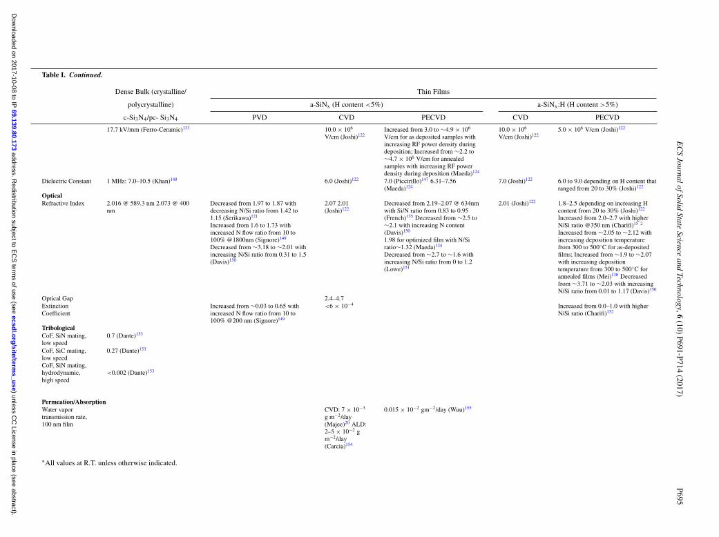
Table I. Continued.
Dense Bulk (crystalline/ Thin Films
polycrystalline) a-SiNx (H content <5%) a-SiNx:H (H content >5%)
c-Si3N4/pc- Si3N4 PVD CVD PECVD CVD PECVD
17.7 kV/mm (Ferro-Ceramic)133 10.0 × 10⁶
V/cm (Joshi)122Increased from 3.0 to ∼4.9 × 10⁶
V/cm for as deposited samples withincreasing RF power density duringdeposition; Increased from ∼2.2 to∼4.7 × 10⁶ V/cm for annealedsamples with increasing RF powerdensity during deposition (Maeda)124
10.0 × 10⁶
V/cm (Joshi)1225.0 × 106 V/cm (Joshi)122
Dielectric Constant 1 MHz: 7.0–10.5 (Khan)148 6.0 (Joshi)122 7.0 (Piccirillo)147 6.31–7.56(Maeda)124
7.0 (Joshi)122 6.0 to 9.0 depending on H content thatranged from 20 to 30% (Joshi)122
OpticalRefractive Index 2.016 @ 589.3 nm 2.073 @ 400
nmDecreased from 1.97 to 1.87 withdecreasing N/Si ratio from 1.42 to1.15 (Serikawa)121
Increased from 1.6 to 1.73 withincreased N flow ratio from 10 to100% @1800nm (Signore)149
Decreased from ∼3.18 to ∼2.01 withincreasing N/Si ratio from 0.31 to 1.5(Davis)150
2.07 2.01(Joshi)122
Decreased from 2.19–2.07 @ 634nmwith Si/N ratio from 0.83 to 0.95(French)135 Decreased from ∼2.5 to∼2.1 with increasing N content(Davis)150
1.98 for optimized film with N/Siratio∼1.32 (Maeda)124
Decreased from ∼2.7 to ∼1.6 withincreasing N/Si ratio from 0 to 1.2(Lowe)151
2.01 (Joshi)122 1.8–2.5 depending on increasing Hcontent from 20 to 30% (Joshi)122
Increased from 2.0–2.7 with higherN/Si ratio @350 nm (Charifi)15 2
Increased from ∼2.05 to ∼2.12 withincreasing deposition temperaturefrom 300 to 500◦C for as-depositedfilms; Increased from ∼1.9 to ∼2.07with increasing depositiontemperature from 300 to 500◦C forannealed films (Mei)130 Decreasedfrom ∼3.71 to ∼2.03 with increasingN/Si ratio from 0.01 to 1.17 (Davis)150
Optical Gap 2.4–4.7ExtinctionCoefficient
Increased from ∼0.03 to 0.65 withincreased N flow ratio from 10 to100% @200 nm (Signore)149
<6 × 10⁻⁴ Increased from 0.0–1.0 with higherN/Si ratio (Charifi)152
TribologicalCoF, SiN mating,low speed
0.7 (Dante)153
CoF, SiC mating,low speed
0.27 (Dante)153
CoF, SiN mating,hydrodynamic,high speed
<0.002 (Dante)153
Permeation/AbsorptionWater vaportransmission rate,100 nm film
CVD: 7 × 10⁻³
g m−2/day(Majee)20 ALD:2–5 × 10⁻² gm−2/day(Carcia)154
0.015 × 10⁻² gm−2/day (Wuu)155
∗All values at R.T. unless otherwise indicated.
) unless CC
License in place (see abstract). ecsd
l.org
/site/terms_u
se address. R
edistribution subject to EC
S term
s of use (see 69.139.80.173
Dow
nloaded on 2017-10-08 to IP
P696 ECS Journal of Solid State Science and Technology, 6 (10) P691-P714 (2017)
Limited commercial success of liquid phase synthesis hasbeen the infiltration of porous ceramics followed by pyrolyticconversion to produce densified ceramic-matrix composites(CMCs),63 as binders in metal-matrix composites (MMCs),64 and asspin-on film for photolithography with materials supplied initially byKion Corp and transitioned to Clariant and E Merck Corp.65 Simi-larly, commercial acceptance was achieved in fabrication of dielectriclayers by spin-on deposition techniques for semiconductor devicesin a process in which silicon nitride initially formed from perhydri-dopolysilazane was ultimately converted to silicon dioxide66,67 withmaterials supplied by Tonen Corp, but this approach has largely beenabandoned.68
Silicon nitride thin film vapor processing technologies.—Sili-con nitride thin film vapor processing technologies include physicalvapor deposition (PVD), primarily sputtering; chemical vapor depo-sition (CVD) in its various forms, including thermal, hot wire (HW-CVD), plasma-enhanced (PE-CVD), and remote plasma-enhanced;and atomic layer deposition (ALD), also in thermal, plasma-assisted(PA-ALD), plasma-enhanced (PE-ALD), and remote plasma forms.In this context, Takeyama,25 King,11,12 and Meng,13 present valuablehistorical reviews of silicon nitride PVD, CVD, and ALD depositiontechniques.
PVD, which in principle involves the transport but not the for-mation of silicon nitride is an area of continued exploration sincefilm composition and properties are influenced by sputtering methodsas well as transport, and deposition environments.69 There is emerg-ing interest and reports of alternatives to ALD for ultra-thin filmsfor both SiNx and SiNxCy by self-limiting processes associated withself-assembled monolayer (SAM) deposition70 and molecular layerdeposition (MLD).68,71,72
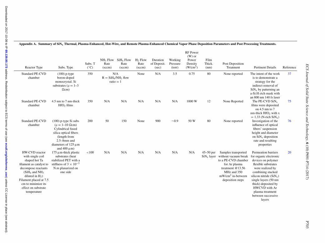
Vapor phase synthesis is associated with the semiconductor, med-ical, aerospace, energy, and automotive sectors. As such, the presentarticle will predominantly review the latest research work in vaporphase synthesis. In this respect, Tables II and III present details ofvery recent vapor phase deposition techniques of SiNx thin films,along with a synopsis of intended applications.15,16,20–25,31–34,36–38,73–101
More specifically, Table II summarizes PVD and CVD work, whileTable III focuses exclusively on atomic layer deposition ALD.
It is worth noting that, historically, CVD in its various forms, in-cluding thermal, HW-CVD, PA-CVD, PE-CVD, and remote plasma-enhanced, had been the method of choice for growing SiNx thinfilms, followed by PVD, mainly magnetron sputtering. More recently,however, ALD (including thermal, PA-ALD, and PE-ALD) appearsto be receiving the most attention due to the need for extremelythin SiNx films with increasingly tight control of composition andproperties.
In what follows, an overview is first presented of silicon nitridesource chemistries. In this context, Table IV outlines the Si- and N-bond dissociation energies for selected SiNx source chemistries102,103
while Table V focuses on relevant properties of many of the recentlystudied CVD and ALD SiNx source precursors.104 Subsequently, thevarious CVD, PVD, and ALD processes are summarized, respectively,in Appendices A, B, and C and discussed in more detail in the relevantsections.
Overview of Silicon Nitride Source Chemistries
It should be noted that in the case of CVD and ALD processes,the differences in formation and behavior of SiNx thin films can beattributed, in part, to fundamental thermodynamic and chemical prop-erties of precursors. In this context, Table IV lists bond dissociationenergies for selected SiNx source chemistries, not only those that aremost commonly used, specifically, silane (SiH4) and ammonia (NH3).The table is intended to provide the reader with a baseline comparisonof bond dissociation energies of selected organic and inorganic Siand N source chemistries with the most commonly used precursors,namely, silane (SiH4) and ammonia (NH3). Table V presents rele-vant properties of many of the recently studied CVD and ALD SiNx
source precursors. The precursors are divided into classes: perhydri-dosilanes, hydridohalosilanes, halosilanes and aminosilanes. Repre-sentative structures are depicted below.
perhydridosilanes (silane, NPS)
hydridohalosilanes (DCS, diiodosilane)
halosilanes (tetraiodosilane, HCDS)
aminosilanes (TSA, BTBAS)
Si H
H
H
HH Si Si Si H
H
HH
HSi HH
H
SiHH
H
SiCl
Cl
H
HSi
I
I
H
H
SiI
I
I
I
Si Si
Cl
Cl
Cl
Cl
Cl
Cl
NH3Si SiH3
SiH3
SiNH
NH
H
H
C
C
CH3H3C
H3C
H3C
H3C CH3
The large bond dissociation energy of N2 and relatively high bonddissociation energy of SiH4 are consistent with the fact that energeticenvironments, typically either thermal or plasma, are necessary forthin film formation. The resulting films tend to be rich in H and theH typically resides on the Si atoms, with post deposition thermaltreatment commonly applied to reduce H content.36,38,41,42 Since theN atom is trivalent and the silicon atom is tetravalent, H content inthe film has minimal effect on the mobility of films: conformalityis difficult to achieve and reflow is not observed in post-depositionprocess windows.34,85,91
In contrast, the lower dissociation energies associated with NH3
and SiI4 allows deposition at lower temperatures.105,106 Additionally,chemical pathways associated with silicon diimide and diiodosily-lene formation from SiI4 are enabled for deposition. In this case, Hmostly resides on the N atom on films formed from silicon halidesand NH3 with the important consequence that the mobility of Hsubstituted N atoms are constrained in two dimensions rather thanthree. Conformality is therefore expected to be easier to achieve.This advantage is offset by the fact that the chemical depositionpathway leads to gas phase depletion reactions independent of thesubstrate.73
The discussion above is partly simplified, particularly in the case ofCVD. Higher energy environments associated with CVD often inducegas phase depletion reactions initiated by unimolecular decompositionof a precursor and/or direct reaction of precursors in the gas phase pre-ceding or concomitant with deposition.107 ALD more often proceedsby direct reaction with surfaces or by a dissociative adsorption onsurfaces (in rate limiting steps) and, as a result, associated reactions,by definition, proceed sequentially.82,90
) unless CC License in place (see abstract). ecsdl.org/site/terms_use address. Redistribution subject to ECS terms of use (see 69.139.80.173Downloaded on 2017-10-08 to IP
ECS Journal of Solid State Science and Technology, 6 (10) P691-P714 (2017) P697
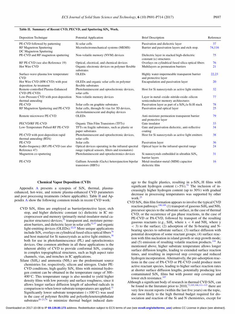
Table II. Summary of Recent CVD, PECVD, and Sputtering SiNx Work.
Deposition Technique Potential Application Brief Description Reference
PE-CVD followed by patterning Si solar cells Passivation and dielectric layer 37RF Magnetron SputteringDC Magnetron Sputtering
Microelectromechanical systems (MEMS) Barrier and passivation layers and etch stop. 74,116
PE-CVD and RF magnetron sputtering Non-volatile memory (NVM) devices Dielectric layer in stacked high-dielectricconstant (κ) structures
75
RF PE-CVD (see also Reference 19) Optical, electrical, and chemical devices Overlays on cylindrical fused silica optical fibers 76Hot Wire CVD Organic electronic devices on polymer flexible
substratesMultilayers as permeation barriers 21
Surface-wave-plasma low temperatureCVD
OLEDs Highly water-impermeable transparent barrierand protective layer
22,23
Hot Wire CVD (HW-CVD) with postdeposition Ar treatment
OLEDs and organic solar cells on polymerflexible substrates
Encapsulation and passivation layer 20
Remote-controlled Plasma-EnhancedCVD (PE-CVD)
Photoluminescent and optoelectronic devices,solar cells
Host for Si nanocrystals as active light emitters 32
Low-Pressure CVD with post-depositionthermal annealing
Non-volatile memory devices Layer in metal–oxide–nitride-oxide–siliconsemiconductor memory architectures
77
PE-CVD Solar cells on graphite substrates Passivation layer as part of a SiNx/a-Si:H stack 78RF Magnetron Sputtering and PE-CVD Solar cells, through-Si vias for 3D devices,
electroluminescent and display devicesPassivation and optical layer 25
Remote microwave PE-CVD OLEDs Anti-moisture permeation transparent barrierand protective layer
79
PECVD/RF PE-CVD Organic Thin Film Transistors (TFTs) Gate insulator 33Low-Temperature Pulsed-RF PE-CVD TFTs on fragile substrates, such as plastic or
paper substratesGate and passivation dielectric, anti-reflectivecoating
34
PE-CVD with post-deposition rapidthermal annealing (RTA)
Photoluminescent and optoelectronic devices,solar cells
Host for Si nanocrystals as active light emitters 38
PE-CVD Solar cells Passivation layer 36Radio-frequency (RF) PE-CVD (see alsoReference 47)
Optical devices operating in the infrared spectralrange (optical sensors, filters and resonators)
Optical layer in the infrared spectral range 24
Magnetron co-sputtering Photoluminescent and optoelectronics devices Si nanocrystals embedded in ultrathin SiNxbarrier layers
31
PE-CVD Gallium Arsenide (GaAs) heterojunction bipolartransistors (HBTs)
Metal-insulator-metal (MIM) capacitordielectric film
16
Chemical Vapor Deposition (CVD)
Appendix A presents a synopsis of SiNx thermal, plasma-enhanced, hot-wire, and remote plasma-enhanced CVD parametersand post processing treatments (where applicable). Table II and Ap-pendix A show the following common trends in recent CVD work:
CVD SiNx films are employed as barrier/protective layer, etchstop, and higher dielectric constant (κ) dielectric in IC mi-croprocessor and memory (primarily metal-insulator-metal ca-pacitor structures) devices;75 transparent and, moisture perme-ation barriers, and dielectric layer in solar cells32,37 and organiclight-emitting devices (OLEDs).22,23 More unique applicationsinclude SiNx overlays on cylindrical fused silica optical fibers76
and host material for Si nanocrystals as active light emitters,38
both for use in photoluminescence (PL) and optoelectronicsdevices. One common attribute in all these applications is theinherent ability of CVD to provide conformal SiNx coatingsin complex topographical structures, such as high aspect ratiochannels, vias, and trenches in IC applications.
Silane (SiH4) and ammonia (NH3) are the predominant sourcechemistries for, respectively, silicon and nitrogen. Under PE-CVD conditions, high quality SiNx films with minimal hydro-gen content can be obtained in the temperature range of 300–400◦C. This temperature range is also needed to yield higherdensity films with low porosity and surface roughness, since itallows longer surface diffusion length of adsorbed radicals incomparison to when lower substrate temperatures are applied.31
Significantly lower substrate temperature (<100◦C) was usedin the case of polymer flexible and polyethyleneterephthalatesubstrates20–23,79 to minimize thermal budget induced dam-
age to the fragile plastics, resulting in a-SiNx:H films withsignificant hydrogen content (>5%).79 The inclusion of in-creasingly higher hydrogen content (up to 30%) with gradualdecrease in processing temperatures was supported by otherwork.25
CVD SiNx thin film formation appears to involve the typical CVDreaction pathways:108,109 (1) transport of gaseous SiH4 and NH3
precursor species to the substrate surface, in the case of thermalCVD, or the occurrence of gas phase reactions, in the case ofPE-CVD or PA-CVD, followed by transport of the resultinggaseous reactants (e.g., SiHx where x < 4 and NHy where y< 3) to the surface; (2) adsorption of the Si-bearing and N-bearing species to substrate surface; (3) surface diffusion withpotential desorption of some reactant groups; (4) surface reac-tion with film nucleation in island growth or step growth mode;and (5) emission of resulting volatile reaction products.110 Asmentioned above, higher substrate temperature allows longersurface diffusion lengths, leading to extended surface reactiontimes, and resulting in improved step coverage and reducedhydrogen incorporation. Alternatively, the pre-adsorption reac-tions in the case of PA-CVD or PE-CVD could produce moreactive reactant species, leading to higher surface reaction ratesat shorter surface diffusion lengths, potentially producing lesscontaminated SiNx films but with poorer step coverage andlower etch resistance.107
Although a significant body of research in thermal CVD SiNx canbe found in the literature prior to 2010,73,105,106,111–115 there arevery few recent reports (within the last five years) on the topic,due most likely to the high thermal budget required for dis-sociation and reaction of the Si and N chemistries, except for
) unless CC License in place (see abstract). ecsdl.org/site/terms_use address. Redistribution subject to ECS terms of use (see 69.139.80.173Downloaded on 2017-10-08 to IP

P698 ECS Journal of Solid State Science and Technology, 6 (10) P691-P714 (2017)
Table III. Summary of Recent ALD SiNx Work.
Deposition Technique Potential Application Brief Description Reference
Thermal ALD Integrated Circuitry (IC) devices Thin films in transistors, memory cells, logic devices,memory arrays
100
Plasma-EnhancedALD (PE-ALD)
IC devices Hydrofluoric acid (HF) etch stop layer and electricallyinsulating spacer
80
PE-ALD IC, MEMS, and biomedical devices HF etch stop layer and electrically insulating spacer 81PE-ALD MOSFET devices Diffusion barrier 82PE-ALD IC devices Gate spacer of dynamic random access memory and
logic devices, and charge trap layer of 3D verticalNAND flash devices
83
PE-ALD IC devices Functional material for logic and memory devices 84PE-ALD IC logic and memory devices Oxidation mask, diffusion barrier, gate dielectric, liner,
and spacer85
Thermal andPlasma-Assisted(PA-ALD)
IC logic and memory devices Nitride spacer, floating gate 86
Thermal ALD Non-volatile memory (NVM) devices Dielectric layer in stacked high-κ structures 87PA-ALD IC devices, photovoltaic devices Dielectric layer, sidewall spacer, hard etch mask,
passivation layer, antireflection coating88
PE-ALD IC memory devices Gate spacers for high κ transistors 92PE-ALD MOSFET devices Spacer material 90PE-ALD Organic light-emitting diodes Encapsulation layer against moisture and O2 permeation 91PE-ALD IC devices Barrier film and masking material 89PE-ALD IC logic and memory devices High κ material, spacer material 93PE-ALD IC devices, photovoltaic devices Anti-reflective coating, passivation and encapsulation
layer, diffusion barriers, gate dielectric, stress liner94
Thermal ALD IC devices passivation layer, barrier for alkali or moisturediffusion, masking layer, final protection layer
95
PE-ALD IC devices Liner and spacer material 96Thermal or PE-ALD IC devices Spacer, mask 101PE-ALD IC devices Spacer, etch stop material 11PE-ALD IC devices Host matrix for Ru nanocrystals as seed/barrier layer for
Cu metallization97,98
Thermal ALD IC devices Dielectric material 117
noteworthy research on the thermal CVD reaction of dichlorosi-lane (SiH2Cl2) and nitrogen (N2). This reaction required a sub-strate temperature of 750◦C, which is prohibitively high formost electronic and solar applications.77
A significant report34 included the use of pulsed RF generatedby modulating a continuous 200Hz low-frequency wave signal
Table IV. Si- and N- Bond Dissociation Energies for Selected SiNxSource Chemistries∗.
Source Precursor Bond Dissociation Energy (kJ/mole)
NitrogenN2 (N-N) 946NH3 (N-H) 435H2NNH2 (N –N) 272
SiliconSiCl4 (Si-Cl) 460H3SiCl (Si-Cl) 456HSiCl3 (Si-H) 394SiH4 (Si-H) 384SiBr4 (Si-Br) 377Si2H6 (Si-H) 374Si2H6 (Si-Si) 321SiI4 (Si-I) 284
∗The table is intended to provide baseline comparisons of bond dis-sociation energies of selected organic and inorganic Si and N sourcechemistries with the most commonly used precursors.102,103
generator with 50% duty cycle in the PE-CVD reaction ofSiH4 and NH3 at 150◦C. The process yielded film densification(over 20% increase in film density) and smoothing (a decreasein average surface grain size standard deviation from 0.2nm2
to 0.04nm2), with the SiNx films exhibiting smoother surfacemorphology and lower void density.
A common rule of thumb32,38,75 in the PE-CVD and PA-CVDwork appears to be that lower R = NH3/SiH4 flow ratios (R <1) lead to Si-rich films (Si/N ratio > 1.1), while higher R (R >1) produces N-rich films (N/Si ratio > 1.4), with inclusions ofSi nanostructures or nanoscale intrusions at even higher R val-ues. Also, lower substrate temperatures tend to yield a-SiNx:Hfilms, with thermal annealing required to reduce H content andlead to film crystallization, while higher processing temper-atures produce c-SiNx films with reduced hydrogen content.Comparable results were obtained in the case of PE-CVD SiNx
from a N2+SiH4 mixture, with Si-rich films being formed athigher N2 flows.75
Studies of post-deposition thermal annealing effects were alsoreported under different annealing modes, gases, and durations,with21 or without vacuum break between the deposition andannealing steps:36,38,41,42
In the case of in situ annealing,21 SiNx multilayered perme-ation barrier stacks deposited on PET substrates <100◦Cwere transported to a PE-CVD chamber between everytwo successive 50-nm thick SiNx layers and exposed toa 13.56 MHz RF Ar plasma at varying power density,working pressure, and treatment duration. The work ledto the identification of an optimized Ar plasma treatment
) unless CC License in place (see abstract). ecsdl.org/site/terms_use address. Redistribution subject to ECS terms of use (see 69.139.80.173Downloaded on 2017-10-08 to IP

ECS Journal of Solid State Science and Technology, 6 (10) P691-P714 (2017) P699
Table V. Relevant Properties of Recently Studied CVD and ALD SiNx Source Precursors.
Molecular Boiling Melting VaporClass Name Acronym Formula Weight % Si form Point Point Pressure Density
◦C ◦C ◦C: torr g/cm−3
Perhydridosilanessilane SiH4 32.12 87.4 gas −112◦ −185◦ −110◦:775 0.680disilane Si2H6 62.22 90.3 gas −14.5◦ −132◦ 21.1◦:2586 0.686trisilane Si3H8 92.32 91.2 liquid 52.9◦ −117◦ 0◦: 95.5 0.743n-tetrasilane Si4H10 122.42 91.7 liquid 106◦ −85 to −95◦ 20◦: 22 0.825isotetrasilane Si4H10 122.42 91.7 liquid 101◦ −99◦ 20◦: 25 0.793neopentasilane NPS Si5H12 152.52 92.1 liquid 132–134◦ <−40◦ 25◦:15 0.805
Hydridohalosilanesmonochlororosilane MCS SiH3Cl 66.56 42.2 gas −30.4◦ 118◦ 25◦: 4900 1.145dichlorosilane DCS SiH2Cl2 101.01 27.8 gas 8.3◦ −122◦ −34◦: 100 1.22diiodosilane DIS SiH2I2 283.91 9.9 liquid 149−150◦ −1◦ 55◦:25 2.834triiodosilane SiHI3 409.81 31.0 liquid 220◦ 8◦ 95◦: 12 3.314
Halosilanestetrachlorosilane SiCl4 169.90 16.5 liquid 57.6◦ −70◦ 20◦: 194 1.481hexachlorodisilane HCDS Si2Cl6 268.89 20.9 liquid 144−6◦ −1◦ 85◦: 109 1.562octachlorotrisilane OCTS Si3Cl8 367.88 22.9 liquid 213–5◦ −67◦ 90◦:10 1.61tetrabromosilane SiBr4 347.70 8.1 liquid 154◦ 5◦ 0◦:1.8 2.772tetraiodosilane SiI4 535.70 5.2 solid 287–8◦ 120–1◦ 125◦:∼30 4.198
Aminosilanestrisilylamine TSA Si3H9N 107.33 78.5 liquid 52◦ −106◦ 0◦: 110 0.895bis(diethylamino)silane BDEAS SiH22C8N2 174.36 16.1 liquid 188–189◦ <0◦ 70◦:30 0.804bis(t-butylamino)silane BTBAS SiH22C8N2 174.36 16.1 liquid 167◦ <−50◦ 25◦: 1.15 0.816tris(dimethylamino)silane 3DMAS SiCH19C6N3 161.32 17.4 liquid 145–8◦ −90◦ 4◦: 16 0.838tris(isopropylamino)silane TIPAS SiH25C9N3 203.40 13.8 liquid 165–166◦ 25◦: 1tetrakis(ethylamino)silane TEAS SiH24C8N4 204.39 13.7 liquid >90◦-dec. <0◦ 25◦: 1.3tetrakis(dimethylamino)silane 4DMAS SiH24C8N4 204.39 13.7 liquid 180◦ −2◦ 75◦: 19 0.885bis(dimethylaminomethylsilyl)-trimethylsilylamine
DTDN-2H2 Si3C9H29N3 263.60 32.0 liquid 237◦ 60◦: 1.0
tris(isopropyl)cyclotrisilazane TICTZ Si3C9H27N3 261.59 32.2 liquid 220–224◦ −69◦ to −71◦ 67◦: 1.8 0.919tetramethyldisilazane TMDZ Si2C4H15N 133.34 42.1 liquid 99–100◦ <−60◦ 25◦: 55 0.766diisopropylaminosilane DIPAS SiC6H17N 131.30 21.4 liquid 117◦ <−20◦ 55◦: 106 0.76
Data in this table from sources cited in text or experimentally determined by the authors.
recipe for the formation of improved permeation barri-ers, with the finding being attributed to the role of Arplasma in rearranging Si and N atoms at the SiNx layersinterfaces, thus causing a densification of the interfacialregions, and an ensuing reduction in the permeability ofthe SiNx multilayered stacks.
In the case of annealing in a conventional oven with vac-uum break, one study41,42 performed annealing of Si-rich SiNx films in a conventional oven in N2 flow, withthermal treatment at 1100◦C leading to the formationof Si nanocrystals (Si-NCs) within the SiNx host ma-trix. The Si-NCs acted to significantly enhance the SiNx
films photoluminescence properties due to quantum con-finement effects. In another study,36 SiNx samples wereannealed in a conventional oven at 830◦C to improve hy-drogen passivation and ensure reduced leakage currentin the resulting metal-insulator-semiconductor (MIS)structures.
Alternatively, another approach38 implemented rapid ther-mal annealing (RTA) with vacuum break in pure Ar, Arwith 20% O2, and Ar with 50% O2 of Si nanoscale in-trusions (Si-ni) embedded in Si-rich SiNx films. It wasfound that only at temperatures above 950◦C did thethermal treatment have any effect on the optical prop-erties of the Si nanoscale intrusions, although the effectwas less significant than the NH3 to SiH4 ratio duringthe deposition step.
Physical Vapor Deposition (PVD)
Appendix B presents a synopsis of SiNx sputtering parametersand post processing treatments (where applicable). A review of TableII and Appendix B shows the following common trends in recentsputtering work:
Most common applications for sputtered SiNx films consist pri-marily of a barrier/passivation coating and etch stop in micro-electromechanical systems (MEMS);74,116 high refractive indexmaterial for solar cells,25 through-Si vias for three-dimensional(3D) semiconductor devices, electroluminescent devices, anddisplay devices;25,31 and high κ dielectric layer in stackedhigh-dielectric constant (κ) structures for non-volatile memory(NVM) devices.75 A unique application is as a host materialfor Si nanocrystals as active light emitters for uses in PL andoptoelectronic devices. Given that sputtering tends to be a lineof sight technique, the application of sputtering techniques isprimarily limited to topographies that are less aggressive withmore relaxed design rules and smaller aspect ratios than theirCVD and ALD counterparts.
DC or RF magnetron sputtering were the deposition techniquesof choice for PVD, although the deposition rates for RF mag-netron sputtered SiNx were significantly lower than their DCcounterparts.74,116 Furthermore, the DC magnetron sputteredSiNx films exhibited superior chemical and physical proper-ties than their RF magnetron sputtered analogs, while dis-playing equivalent electrical characteristics in MEMS devices.
) unless CC License in place (see abstract). ecsdl.org/site/terms_use address. Redistribution subject to ECS terms of use (see 69.139.80.173Downloaded on 2017-10-08 to IP

P700 ECS Journal of Solid State Science and Technology, 6 (10) P691-P714 (2017)
These findings support the conclusion that DC magnetron sput-tered films are more suitable than their RF equivalents for mostSiNx applications, except in cases where substrates are me-chanically or chemically fragile, thus requiring reduced impactenergy to minimize ion and radical Induced damage.
In DC magnetron sputter work,116 it was shown that the N2 plasmaback pressure played a key role in modulating the N/Si ratio inthe resulting SiNx films, with higher back pressures leading toincreased N content in the films. Alternatively, in another report,the N/Si ratio in SiNx films was controlled by employing RFMagnetron sputtering to produce Si-rich films, and PE-CVD toyield N-rich films.74
A pertinent report25 compared the properties of SiNx films grownby RF magnetron sputtering and PE-CVD at low temperature.The resulting findings indicated that sputtering was more ap-propriate than PE-CVD in yielding higher quality SiNx filmswith enhanced density, with the lower density in the PE-CVDcoatings being attributed to the inclusion of hydrogen (due tothe lower processing temperature employed).25
Another report of note31 focused on the formation of Si nanocrys-tals (Si-NC) in multilayered structures consisting of alternatingSi-rich SiNx (SRN) and Si3N4 ultrathin films. In this case, theN/Si ratio in the SRN layers was regulated by co-sputteringfrom Si (DC magnetron sputtering) and Si3N4 (RF magnetronsputtering) targets. The Si content in the resulting SRN filmswas modulated by adjusting the deposition rates from the tar-gets through control of the power applied to the targets, withthe application of higher DC power to the Si target leading toan increase in Si concentration. Alternatively, stoichiometricSi3N4 ultrathin films were achieved by RF magnetron sputter-ing from the stoichiometric target. After the formation of 25alternating layers consisting of 5 nm thick SRN and 1nm thickSi3N4, the structures were capped with a 10 nm-thick Si3N4
protective coating and annealed above 900◦C in N2 environ-ment to form Si-NCs in the Si-rich layers. The annealing stepled to improved PL performance, which was attributed to im-proved crystallization and enhanced nitride passivation in theSi-rich layers.
Atomic Layer Deposition (ALD)
Appendix C presents a synopsis of SiNx thermal, plasma-assisted,and plasma-enhanced ALD parameters and post processing treat-ments (where applicable). A simple first-order observation is thatunder similar conditions, regardless of technique, growth per cycle(GPC) is significantly greater with precursors containing multiple sil-icon atoms. For example, neopentasilane has a higher growth ratethan silane. Similarly, hexachlorodisilane has a higher growth ratethan dichlorosilane.113 Table III and Appendix C reveal the followingadditional trends in recent ALD work:
The most common applications for ALD SiNx films are bar-rier/protective layer, etch stop, passivation layer, spacer ma-terial, and high dielectric constant (κ) dielectric in emergingnanoscale IC microprocessor and memory devices100 and, to alesser extent, transparent barrier, anti-reflective coating, anti-moisture permeation layer, and dielectric layer in solar cell andOLED systems.88 Other applications include host matrix forruthenium nanocrystals as seed/barrier layer for copper met-allization in IC structures;97,98 and hydrofluoric acid etch stoplayer and electrically insulating spacer in MEMS and medicaldevices.80,81 One common attribute in all these applications isthe inherent ability of ALD to provide stringent atomic levelcontrol and excellent conformality55 for SiNx coatings in chal-lenging geometries where CVD begins to show its deficien-cies and shortcomings. These geometries include highly com-plex topographical structures, such as extremely high aspectratio or exceedingly narrow channels, vias, and trenches in ICapplications.
In contrast to recent CVD work, very few ALD reports usedSiH4 and other perhydridosilanes, such as neopentasilane((SiH3)4Si), as Si source chemistry.11,85 Instead, the Si sourcesemployed in the most recent ALD investigations could beorganized into two categories: (a) inorganic Si sources, in-cluding hydridosilanes, such as monochlorosilane (SiH3Cl),93
dichlorosilane (SiH2Cl2),93 and diiodosilane (SiH2I2);101 andhalosilanes, such as hexachlorodisilane (Si2Cl6),82,88,117 Oc-tachlorotrisilane (Si3Cl8),87 and tetraiodosilane (SiI4);86,100,101
and (b) organic Si sources, primarily amidosilanes, such as BT-BAS (SiN2C8H22).92,93 For nitrogen, the majority of the workdescribed the use of NH3 or N2. One report suggested the ad-ditional use of hydrazine (N2H4),101 which is quite undesirablegiven its elevated toxicity and high instability, while anotherproposed the utilization of t-butylhydrazine (C4H12N2).100 Al-though no dissociation energy is available in the literature fort-butylhydrazine, it is estimated to be significantly lower thanN2 based on reports in the literature on the dissociation energyof N2H2,103 thus making t-butylhydrazine more conducive forALD growth of SiNx at lower temperatures than N2.
ALD SiNx work86,87,100,117 was carried out in three different modes:thermal (no plasma), PA-ALD (where the plasma was generatedin the reactor directly above the substrate), and PE-ALD (wherethe plasma was generated remotely and transported into thereactor).
For thermal ALD, the majority of the work focused on the reactionof halosilanes and N-bearing reactants, including: (a) SiI4 andNH3 or C4H12N2 in the temperature range of 175–250◦C;100
(b) Si halides containing Br and/or I (e.g., SiI4, SiBr4, SiBr4-xIx
(x = 1–3), or SiyX2y+2, where y > 2, and X is one or more Br orI) and a N-containing reactant, such as NH3, in the temperaturerange of 350–600◦C;86 (c) Si3Cl8 and NH3 in the temperaturerange of 310–500◦C;87 (d) Si2Cl6 and NH3 in the temperaturerange of 515–573◦C.117 Only two of the reports87,117 presentedcompositional analysis results for the SiNx films. The findingsindicated that lower deposition temperatures produced sub-stoichiometric films that oxidized upon exposure to air. Higherprocessing temperatures generated films that were closer to aN/Si ratio of ∼1.3, and led to a reduction but not complete elim-ination of oxidation upon removal from the ALD reactor. Theseresults suggest that thermal ALD might require prohibitivelyhigher deposition temperatures (well above 573◦C) to yieldstoichiometric films with effective resistance to oxidation.
PA-ALD SiNx is the subject of relatively few reports,86,88 and thework focused on the reaction of halosilanes and N-bearing re-actants, primarily: (a) Si halides containing Br and/or I (Seesection Overview of silicon nitride source chemistries) and aN-containing reactant, such as NH3, in the temperature rangeof 350–600◦C;86 and (b) Si2Cl6 and NH3 in the temperaturerange 350–450◦C.88 The apparent lack of interest in PA-ALDSiNx could be attributed, at least in part, to concerns about thepotential adverse effects of plasma generation directly abovethe substrate, including the potential inclusion of contaminantsin the films. Furthermore, compositional analysis88 showed thatthe PA-ALD films were N-rich (N/Si ratio ∼1.71) with signif-icant H incorporation (e.g., as high as 23% at 400◦C). Infraredstudies88 supported the preferential reaction of Si2Cl6 with sur-face NH2 clusters, instead of NH groups, with the latter beingincorporated in the SiNx films due to their reduced reactivitywith Si2Cl6. Interestingly, the infrared analysis demonstratedthat the inclusion of H in the films was primarily in the formof NH species. This is consistent with earlier reports of Atmo-spheric Pressure CVD (APCVD) silicon nitride generated fromiodosilanes.105,106
Most recent ALD work consisted of plasma assisted process-ing, wherein the plasma was generated remotely and trans-ported into the reactor.11,79–85,89–94,96–98,100,101,117 The bene-fits of remote plasma include lower deposition temperatureswhile ensuring minimal plasma-induced damage, exclusion of
) unless CC License in place (see abstract). ecsdl.org/site/terms_use address. Redistribution subject to ECS terms of use (see 69.139.80.173Downloaded on 2017-10-08 to IP
ECS Journal of Solid State Science and Technology, 6 (10) P691-P714 (2017) P701
undesirable gas-phase reactions, and reduction in surface nu-cleation time. As mentioned above, the Si sources employed inPE-ALD investigations could be organized into two categories:(a) inorganic Si sources, including perhydridosilane, hydridosi-lanes and halosilanes and (b) organic Si sources, primarilyamidosilanes.
A number of reports examined the role of substrate temperaturein PE-ALD SiNx, with primary focus on the effects of lowthermal budget on PE-ALD process characteristics and result-ing film composition and chemical and electrical properties.One such report investigated low temperature PE-ALD growthfrom bis(t-butylamino)silane (BTBAS) and a N2+Ar plasma at150◦C.91 Subsequent structural and chemical characterizationof the SiNx layers indicated the absence of open pores largerthan 0.3nm in diameter, with films as thin as 10 nm displayinggood barrier properties. A second investigation examined lowtemperature PE-ALD (<300◦C)85 of SiNx films from neopen-tasilane (NPS) as source chemistry using trisilylamine (TSA)as comparative baseline. The study determined that both pre-cursors exhibited similar N2 plasma saturation behavior, withNPS displaying higher growth rates. The films were Si rich(Si/N ratio ∼1.13) with minimal O and C contaminants. Athird study94 analyzed the thermal dependence of PE-ALDSiNx films grown from trisilylamine (TSA) and NH3 in thetemperature range 250–350◦C. All the films were nearly stoi-chiometric (N/Si ratio increased from 1.32 at 250◦C to 1.35 at350◦C). Alternatively, hydrogen content decreased from ∼13%to ∼8% with the rise in thermal budget. In terms of higher tem-perature growth, processing temperatures of 400◦C and 500◦Cwere used in the PE-ALD of SiNx from NH3 and, respec-tively, monochlorosilane (MCS) and dichlorosilane (DCS).93
The work demonstrated that the resulting SiNx spacer (grown at400◦C) and gate encapsulation (deposited at 500◦C) were cru-cial components in successful high-κ metal gate applications.Similar findings were presented100 for PE-ALD SiNx from Siprecursors containing an iodine ligand (such as HSiI3, H2SiI2,or H3SiI) and a N-containing plasma. The resulting N/Si ratioranged from 0.5 to 2.0. The findings are consistent with priorwork that employed tetraiodosilane and titanium tetraiodide togenerate Ti-Si-N diffusion barriers for copper metallization atlow temperatures.73
In terms of the PE-ALD adsorption and decomposition mech-anisms for inorganic sources, one relevant report82 analyzedthe reactivity of β-Si3N4 surface sites with Si2Cl6 (using SiH4
as comparative baseline) during the PE-ALD Si2Cl6 substrateexposure step by combining ab initio density functional the-ory calculations with actual PE-ALD SiNx film deposition.The analysis examined three types of substrate surface sites:(a) hydrogen passivated N and Si sites (NH/SiH); (b) NH andSiNH2 sites formed during the NH3 exposure step (NH/SiNH2);and (c) under-coordinated bare Si=N sites. It was determinedthat the bare Si=N sites were more energetically favorablethan their NH/SiH and NH/SiNH2 counterparts to react withthe Si or Cl atoms from the source precursors. It was alsoconcluded that the reaction energy was lower for Si2Cl6 thanSiH4. These findings led to the identification of a 3 step PE-ALD process to attain the most energetically favorable sur-face sites during the Si source PE-ALD substrate exposurestep.82 Another investigation11 also explored the role of a N2
plasma pre-treatment prior to the SiH4 exposure step on Si sub-strates and found that atomic N and N+ are the central reactantspecies that adsorb to the Si surface to form Si-N. The latterthen act as reactive adsorption spots for SiH4 at N danglingbond sites, generating adsorbed SiHx and NHx species. Fur-ther adsorption is excluded until subsequent exposure to theN2 plasma, leading to a repetition of the previous N speciesadsorption cycle. Reiterating the alternating N2 plasma/SiH4
exposure steps results in the growth of a complete Si-N layerfollowed by the formation of a continuous SiNx film. This alter-
nating exposure process was applied to produce SiNx:H filmswith enhanced conformality and improved moisture barrierbehavior.
In terms of the PE-ALD adsorption and decomposition mech-anisms for organic sources, a similar theoretical and exper-imental study82 of the energies of adsorption and decom-position of bis(dimethylaminomethylsilyl)trimethylsilylamine(DTDN2-H2, C9H29N3Si3) during DTDN2-H2 exposure stepon the growing PE-ALD SiNx film surface. The bare Si=Nsites (as formed by the N2 plasma) were found to be themost energetically favorable for the adsorption and reactionof DTDN2-H2. The study also showed that the N/Si ratio inthe films increased from 0.98 to 0.99 as the substrate temper-ature was raised from 300◦C to 400◦C, with oxygen content∼7.5% due to oxidation upon exposure to air. Further increasein substrate temperature to 500◦C caused higher C incorpora-tion, as well as a significant increase in O content. Alterna-tively, another study90 combined first-principles density func-tional theory with experimentation to examine the effects ofN-bearing plasmas (N2, H2, N2-H2, NH3) on the mechanismsof adsorption of bis(t-butylamino)silane (BTBAS, SiN2C8H31)on β-Si3N4 (0001) surfaces with various surface terminations.The study concluded that the use of H2, N2-H2, and NH3 plas-mas caused termination of reactive β-Si3N4 (0001) surface siteswith H and NHx species, thus inhibiting precursor adsorptionand film formation. The study also determined that the applica-tion of a N2 plasma did regenerate reactive surface sites termi-nated with H and NH2 groups. Interestingly, a complementaryinvestigation92 for PE-ALD SiNx from BTBAS pointed to theexistence of so-called “redeposition effects” resulting from thedissociation of reaction species in the plasma and the redeposi-tion of fragments of such species on the surface of the growingSiNx film. It was found that this effect is driven primarily by theplasma gas residence time, with a shorter residence time lead-ing to a reduction in re-deposition effects and yielding films ofhigher purity and improved quality.
A report of note96 incorporated ab initio techniques into theoret-ical models to examine the effects of PE-ALD reaction mech-anisms on precursor adsorption and decomposition pathwaysfor a variety of inorganic and organic Si precursors, includingSiH4, SiH2Cl2, SiH2(CH3)2, (Si3N4)4(NH3)12, and SiN2C8H22.The techniques employed realistic cluster models of amine-covered surfaces to derive the configurations and energies ofchemisorption and reaction of these Si sources via functionalgroups removal. These calculations were combined with den-sity functional theory derivations that determined that the initialprecursor physisorption phase was essential toward SiNx filmformation, which led to accurate predictions regarding the reac-tivity of a collection of amino-silane precursors. The theoreticalderivations also provided correct projections on H retention inthe PE-ALD SiNx films. A recent report used density func-tional theory to model the dissociative chemisorption of siliconnitride precursors (mono(alkylamino)silanes) on silicon diox-ide to determine the effect of different aminoalkyl ligands.118
Adsorption energies, driven primarily by hydrogen bonding didnot vary significantly with size of aminoalkyl ligands, however,a large variation in the reaction energy barriers was observedwith ligand size due to transition state interactions and stericeffects. The ALD window for suitable thin film growth wasfound to be widest for diisopropylaminosilane (DIPAS) anddipropylaminosilane (DPAS) precursors (∼100◦C–500◦C).
Another report97,98 of note developed a PE-ALD SiNx process aspart of forming RuSiNx films as diffusion barriers for copper(Cu) interconnects for IC applications. The process employedtris(isopropylamino)silane (TIPAS) and NH3 for SiNx. RuSiNx
films with varying Ru/SiNx ratios were formed by controllingthe number of PE-ALD SiNx formation cycles while main-taining that for PE-ALD Ru constant. The resulting RuSiNx
ternary phase consisted of an amorphous SiNx host matrix con-
) unless CC License in place (see abstract). ecsdl.org/site/terms_use address. Redistribution subject to ECS terms of use (see 69.139.80.173Downloaded on 2017-10-08 to IP

P702 ECS Journal of Solid State Science and Technology, 6 (10) P691-P714 (2017)
taining Ru nanoclusters of ∼3 nm in diameter, and exhibitedstable diffusion barrier performance against Cu diffusion up to650◦C.
Studies of pre-, during, and post-deposition plasma treatment ef-fects were also reported under different treatment modes, gases,and durations, with and without vacuum break between the de-position and treatment steps. Some of the key findings arereported below:
In the case of pre-deposition plasma treatment, substrateexposure to Ar plasma prior to SiNx thermal ALD wasshown to yield significantly lower SiNx wet etch rates(WERs) compared to the case of no plasma treatment.86
Alternatively, the opposite effect was observed in thecase of a post-deposition H2 plasma treatment,81 whichwas attributed to the role of H2 plasma in removingcontaminants from the film or causing its densification.A similar finding was reported in the post-depositiontreatment in a H2 plasma for 3 hours at 350◦C, whichwas ascribed to the efficacy of the H2 plasma at residualC removal from the films.
Ar plasma was also observed to improve surface adsorptionand activation pathways for PE-ALD SiNx from DIPASand NH3.84 In this work, successful SiNx low temper-ature chemisorption (325◦C) was achieved through theapplication of an additional Ar plasma treatment stepafter the Si precursor purge step, but prior to the NH3
exposure cycle. However, when the intermediate numberof Ar plasma treatments was increased from 1 to 3, theresulting films exhibited a rise in C and O contaminationfrom, respectively, 0 to 10% and ∼15 to 30%. The filmswere Si rich with Si/N ratio over 2.
Alternatively, in PE-ALD of SiNx from BTBAS and N2,92
it was shown that a constant increase in N2 plasma ex-posure time led to a continuous decrease in C contentat lower deposition temperatures (<500◦C). For exam-ple, for films grown at 200◦C, C content decreased from∼15% at 1s N2 plasma exposure time to ∼8% at 15sN2 plasma exposure time. Films formed at N2 plasmaexposure times below 15s showed high affinity to O,while those deposited at 15s exhibited good resistanceto oxidation. However, the composition of SiNx filmsgrown at 500◦C was nearly stoichiometric (Si3N4), withminimal O and C contents, irrespective of N2 plasmaexposure time.
Summary and Commentary
The authors have presented an overview of the most recent pub-lished work (last five years or so) for SiNx and SiNx-rich films, pri-marily SiNx with C inclusion, SiNx(C). This survey highlights majoremerging developments in the SiNx material system technologies,with focus on Si and N source chemistries and thin film depositionprocesses and their effects on resulting properties. It also demonstratesthat SiNx is the subject of an ever-growing interest and that its use isexpanding into new technological areas.
From a chemistry perspective, and while generalizations are dif-ficult when such a wide range of SiNx applications is considered,certain trends are observed. Traditionally, SiNx deposition, particu-larly in IC devices, utilized Si- and N-rich precursors such as SiH4
and N2 in relatively high-energy environments (>700◦C or the useof plasma activation to achieve deposition at lower substrate tem-peratures). More recently, there has been a continual push towardlower energy deposition processes (reduced processing temperature)driven by the need to minimize thermal budget induced damage to
thermally fragile substrates, such as low dielectric constant (κ) ma-terials in IC devices and polymer materials in OLED applications.This need has engendered the utilization of precursors that possess“pre-assembled” Si-N bonds as exemplified by “single-source” pre-cursors such as trisilylamine and, in order to achieve deposition in evenlower energy environments, precursors that contain C, such as bis(t-butylamino)silane. Concomitant with this trend, there was recognitionthat desirable dielectric or passivation properties could be achieveddespite the adventitious incorporation of C into films. Functional orperformance properties, independent of a simple compositional defi-nition of SiNx, expanded interest in reproducible film formation withcontrolled and reproducible C inclusion. Silicon carbonitride filmsbecame widely accepted and deposition techniques and conditionswere explored. As dimension constraints became tighter and ALDtechniques became generally accepted, the differences in gas-phaseand substrate reactivity with Si-N, Si-C, C-N and Si-halide bonds havebeen exploited and furthered the evolution and introduction of newprecursors.
Another independent trend that is readily recognized is the ac-ceptance of silicon halides as precursors. Historically, while siliconhalides react with ammonia and other amines at low temperature, thusmaking them attractive for lower energy deposition processes, the lowgravimetric percentage of silicon in precursors and the troublesomeammonium salt byproducts would have eliminated them from consid-eration. The acceptance of hexachlorodisilane as a SiNx precursor infull-scale manufacturing is leading to consideration of other siliconhalides such as tetraiodosilane in near-term full-scale manufacturing.Inherent in the development of SiNx films is the evolution of SiNx asan encompassing descriptor of the technology to Si-N rich films, suchas SiNx with C inclusion, SiNx(C), as well as the precursors and thedeposition techniques used to achieve these films.
From a processing perspective, CVD in its various forms, includ-ing thermal, hot wire (HW-CVD), plasma-enhanced (PE-CVD), andremote plasma-enhanced CVD, had been historically the method ofchoice for growing SiNx thin films, followed by physical vapor deposi-tion (PVD), primarily magnetron sputtering. More recently, however,ALD has been receiving the most attention due to the need for ex-tremely thin SiNx films with tight control in composition and proper-ties. This trend is attributed to the inherent ability of ALD to providestrict atomic level control and excellent conformality for SiNx thinfilms in aggressive geometries where CVD begins to suffer from poorstep coverage. These geometries include highly complex topograph-ical structures, such as extremely high aspect ratio or exceedinglynarrow channels, vias, and trenches in IC applications.
Another trend that has contributed to the growth of interest in Si-Nrich films is the area of heterodevices. Until now, the primary driverfor thin film materials has been the manufacture of IC devices. Despitethe enormous scholarly literature in virtually every area of thin filmtechnology for microelectronics, there has been little opportunity fornew techniques to achieve adoption in full-scale IC manufacturing.Heterodevices, particularly those associated with life sciences, havedifferent sets of material requirements and can be successful at lowermanufacturing scale. Heterodevices open a wide range of new com-mercialization opportunities for silicon nitrogen-rich materials. Thefield of Si-N rich films will continue to evolve with new film require-ments, new techniques such as Molecular Layer Deposition (MLD)and Self-Assembled Monolayers (SAMs) and associated new Si- andN- precursors.
Acknowledgments
The authors thank Sean King for his invaluable input and helpfuldiscussions.
) unless CC License in place (see abstract). ecsdl.org/site/terms_use address. Redistribution subject to ECS terms of use (see 69.139.80.173Downloaded on 2017-10-08 to IP
EC
SJournalofSolid
StateScience
andTechnology,6
(10)P691-P714
(2017)P703
Appendix A. Summary of SiNx Thermal, Plasma-Enhanced, Hot-Wire, and Remote Plasma-Enhanced Chemical Vapor Phase Deposition Parameters and Post Processing Treatments.
Reactor Type Subs. TypeSubs. T
(◦C)
NH3 FlowRate
(sccm)
SiH4 FlowRate
(sccm)
H2 FlowRate
(sccm)
Durationof Deposit.
(sec)
WorkingPressure
(torr)
RF Power(W) orPower
Density(W/cm2)
FilmThick.(nm)
Post DepositionTreatment Pertinent Details Reference
Standard PE-CVDchamber
(100) p-typeboron-doped
monocrystal. Sisubstrates (ρ = 1–3
�cm)
350 N/AR = SiH4/NH3 flow
ratio = 1
None N/A 3.5 0.75 80 None reported The intent of the workis to demonstrate a
strategy for theindirect removal of
SiNx by patterning ana-Si:H etch mask withan 800 nm 140 fs laser
37
Standard PE-CVDchamber
4.5 nm to 7 nm-thickHfO2 films
350 N/A N/A N/A N/A N/A 1000 W 12 None Reported The PE-CVD SiNxfilms were deposited
on 4.5 nm to 7nm-thick HfO2 with x= 1.33 (N-rich SiNx)
75
Standard PE-CVDchamber
(100) p-type Si subs(ρ = 1–10 �cm)Cylindrical fused
silica optical fibers(length from2.5–8mm and
diameters of 125 μmand 400 μm)
200 50 150 None 900 ∼0.9 50 W 80 None reported Investigation of theinfluence of opticalfibers’ suspension
height and diameteron SiNx depositionrate and resulting
properties
76
HW-CVD reactorwith single coilshaped hot Ta
filament as catalyst todecompose reactants
(SiH4 and NH3diluted in H2)
Filament placed at 7.5cm to minimize itseffect on substrate
temperature
175 μm-thick plasticsubstrates (heat
stabilized PET with astiffness of 3 × 10⁻³
N.m planarized onone side
<100 N/A N/A N/A N/A N/A N/A 45–50 perSiNx layer
Samples transportedwithout vacuum breakto a PE-CVD chamber
for Ar plasmatreatment @13.56
MHz and 350mW/cm2 in-between
deposition steps
Permeation barriersfor organic electronicdevices on polymerflexible substrateswere realized by
combining stackedsilicon nitride (SiNx)single layers (50 nmthick) deposited byHWCVD with Arplasma treatment
between successivelayers
20
) unless CC
License in place (see abstract). ecsd
l.org
/site/terms_u
se address. R
edistribution subject to EC
S term
s of use (see 69.139.80.173
Dow
nloaded on 2017-10-08 to IP

P704E
CS
JournalofSolidState
Scienceand
Technology,6(10)
P691-P714(2017)
Appendix A. Continued.
Reactor Type Subs. TypeSubs. T
(◦C)
NH3 FlowRate
(sccm)
SiH4 FlowRate
(sccm)
H2 FlowRate
(sccm)
Durationof Deposit.
(sec)
WorkingPressure
(torr)
RF Power(W) orPower
Density(W/cm2)
FilmThick.(nm)
Post DepositionTreatment Pertinent Details Reference
CVD reactor with Arwave plasma
generated near thesurface of a dielectricalumina window with
a microwavefrequency of 2.45
GHz Distancebetween alumina
window and substratestage set at 200 mm
25 μ-thick polyimidebase substrates
90 500 70(mixed with 350
sccm Ar)
None 360 75 × 10−3 1.57W/cm2
50 None reported Prior to deposition,polyimide base film wasbaked at 100◦C for 30
min in a glove box withmoisture and oxygen
maintained at less than0.1 ppm, then directly
transferred from the glovebox to the SWP-CVD
system without exposureto the air.
23, 22
HW-CVD reactorwith Ta filamentGlow-discharge
(PECVD) chamberfor sequences of SiNxsingle layers with Ar
plasma surfacetreatment betweenindividual layersdeposition steps
PET substrates 100 varied 2 54 360 25 × 10−3 0.35W/cm2
(for Arplasma
treatment@50
mTorronly)
50 None reported For multilayered SiNxdepositions, samples
transferred back and forthbetween HWCVD to
PECVD chamber withoutbreaking vacuum between
deposition stepsFor Ar treatment, samples
were clamped to topelectrode and heated to
100◦C and bottomelectrode wasRF-powered
Optimal SiNx growthconditions achieved byvarying 3 parameters:
Hydrogen dilution, ratioof NH3 to SiH4, and Tafilament current. Single
and multi-layer SiNxfilms grown (the latterwith intermediate Ar
plasma treatment steps)
20
Remote-controlledPE-CVD chamber
〈100〉 p-type Sisubstrates
300 varied (6.3to 14sccm)
14 N/A 1800 N/A N/A N/A SiNx samplestransferred from
PECVD to conventionalfurnace with vacuum
break SiNx filmsannealed in N2 flow
Annealing temperature:varied from
700–1100◦C AnnealingDuration: 30–60 mins
Excess Si in Si-rich SiNxfilms controlled by
varying the NH3/ SiH4flow ratio between 0.45 to
1.0
32
) unless CC
License in place (see abstract). ecsd
l.org
/site/terms_u
se address. R
edistribution subject to EC
S term
s of use (see 69.139.80.173
Dow
nloaded on 2017-10-08 to IP

EC
SJournalofSolid
StateScience
andTechnology,6
(10)P691-P714
(2017)P705
Appendix A. Continued.
Reactor Type Subs. TypeSubs. T
(◦C)
NH3 FlowRate
(sccm)
SiH4 FlowRate
(sccm)
H2 FlowRate
(sccm)
Durationof Deposit.
(sec)
WorkingPressure
(torr)
RF Power(W) orPower
Density(W/cm2)
FilmThick.(nm)
Post DepositionTreatment Pertinent Details Reference
Low-pressure CVDstandard reactor
p-type (100) Sisubstrates 5 nm-thick
SiO2 thin films onp-type (100) Si
substrates
750 N/A NoneSiCl2H2
used as Sisource
(flow rate:N/A)
None N2used (flowrate: N/A)
N/A 0.6 100 33–231 None reported SiNx films weredeposited directly on
a 5 nm-thick SiO2thin films on p-type
(100) Si
77
PE-CVD standardchamber with a
working frequency of2.45 GHz
a-Si:H substrates N/A N/A N/A N/A N/A 25 × 10−3 1000 80 None reported SiNx films withrefractive index of
1.5–1.8 were used asantireflection coating
78
PE-CVD Chamber HF solution rinsedSi(100) wafers
200–400 N/A N/A N/A N/A 0.6 100 100–500 None reported RF Sputtered SiNxfilms were of higher
density than theirPECVD counterparts
25
Linear microwaveplasma batch
processing systemwith a working
frequency of 2.45GHz Two deposition
modes: Low total flowrate and high total
flow rate
c-Si, UV curedacrylates and PEN
substrates
100 Low total flow rate (400sccm)
R = SiH4/NH3 flowratio = 0.05–0.5
None Arused (flowrate: 200
sccm)
180–1020secs
6 × 10⁻² 1000W/m2
79–100 None reported The films werea-SiNx:H
79
110 High total flow rate(600 sccm)
R = SiH4/NH3 flowratio = 0.05–0.5
None Arused (flowrate: 200
sccm)
105–700secs
8.5 × 10⁻² 835 W/m2 101–175 None reported The films werea-SiNx:H
Standard PE-CVDchamber
N/A N/A N/A N/A N/A N/A N/A N/A N/A None reported Excellent reliabilityshown for vanadyl-
phthalocyanine(VOPc) thin filmtransistors (TFTs)with SiNx as gate
insulator
33
Pulsed RF with a lowfrequency (200 Hz)
square wave envelopePECVD chamberPulsed-RF supply
generated bymodulating a
continuous wave(CW) RF supplyusing the 200 Hz
signal generator with50% duty cycle
c-Si substrates 150 40 4 120 N/A 0.8 130mW/cm2
N/A None reported 200 Hz modulationused to ensure that the
duration of theoff-cycle (2.5ms) issignificantly shorter
than the gas residencetime (∼1s) and
achieve a growth ratethat is 1
2 of that forCW-RF growth
34
) unless CC
License in place (see abstract). ecsd
l.org
/site/terms_u
se address. R
edistribution subject to EC
S term
s of use (see 69.139.80.173
Dow
nloaded on 2017-10-08 to IP
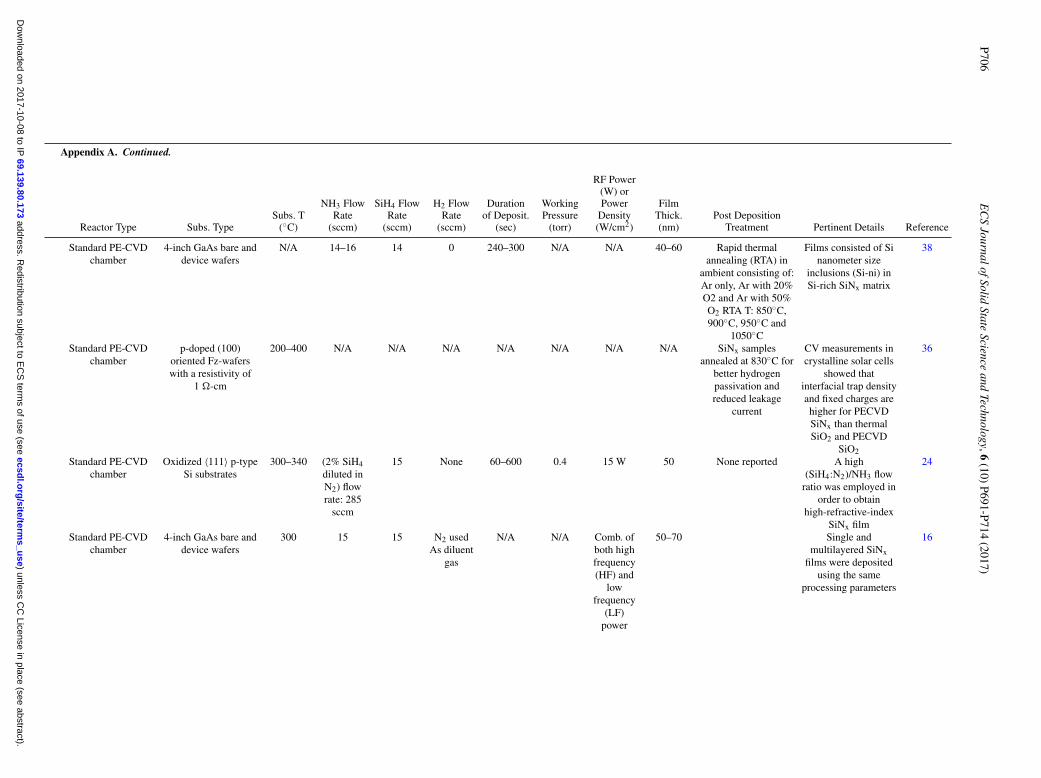
P706E
CS
JournalofSolidState
Scienceand
Technology,6(10)
P691-P714(2017)
Appendix A. Continued.
Reactor Type Subs. TypeSubs. T
(◦C)
NH3 FlowRate
(sccm)
SiH4 FlowRate
(sccm)
H2 FlowRate
(sccm)
Durationof Deposit.
(sec)
WorkingPressure
(torr)
RF Power(W) orPower
Density(W/cm2)
FilmThick.(nm)
Post DepositionTreatment Pertinent Details Reference
Standard PE-CVDchamber
4-inch GaAs bare anddevice wafers
N/A 14–16 14 0 240–300 N/A N/A 40–60 Rapid thermalannealing (RTA) in
ambient consisting of:Ar only, Ar with 20%O2 and Ar with 50%O2 RTA T: 850◦C,900◦C, 950◦C and
1050◦C
Films consisted of Sinanometer size
inclusions (Si-ni) inSi-rich SiNx matrix
38
Standard PE-CVDchamber
p-doped (100)oriented Fz-waferswith a resistivity of
1 �-cm
200–400 N/A N/A N/A N/A N/A N/A N/A SiNx samplesannealed at 830◦C for
better hydrogenpassivation andreduced leakage
current
CV measurements incrystalline solar cells
showed thatinterfacial trap densityand fixed charges arehigher for PECVDSiNx than thermalSiO2 and PECVD
SiO2
36
Standard PE-CVDchamber
Oxidized 〈111〉 p-typeSi substrates
300–340 (2% SiH4diluted inN2) flowrate: 285
sccm
15 None 60–600 0.4 15 W 50 None reported A high(SiH4:N2)/NH3 flow
ratio was employed inorder to obtain
high-refractive-indexSiNx film
24
Standard PE-CVDchamber
4-inch GaAs bare anddevice wafers
300 15 15 N2 usedAs diluent
gas
N/A N/A Comb. ofboth highfrequency(HF) and
lowfrequency
(LF)power
50–70 Single andmultilayered SiNx
films were depositedusing the same
processing parameters
16
) unless CC
License in place (see abstract). ecsd
l.org
/site/terms_u
se address. R
edistribution subject to EC
S term
s of use (see 69.139.80.173
Dow
nloaded on 2017-10-08 to IP
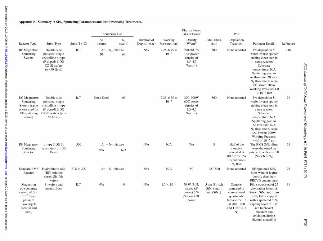
EC
SJournalofSolid
StateScience
andTechnology,6
(10)P691-P714
(2017)P707
Appendix B. Summary of SiNx Sputtering Parameters and Post Processing Treatments.
Sputtering GasPlasma Power(W) or Power Post
Reactor Type Subs. Type Subs. T (◦C)Ar
(sccm)N2
(sccm)Duration of
Deposit. (sec)Working
Pressure (torr)Density(W/cm2)
Film Thick.(nm)
DepositionTreatment Pertinent Details Reference
RF MagnetronSputtering
System
Double-sidepolished, single
crystalline n-type(P doped) 〈100〉
CZ-Si wafers(ρ>50 �cm)
R.T. Ar + N2 mixture N/A 2.25–6.75 ×10⁻³
300–900 W(RF powerdensity of1.5–4.5W/cm2)
500 None reported Pre-deposition Siwafer inverse sputteretching clean step in
same reactor:Substrate
temperature: N/ASputtering gas: Ar
Ar flow rate: 20 sccmN2 flow rate: 0 sccm
RF Power: 200WWorking Pressure: 4.0
× 10−3 torr
11620 60
DC MagnetronSputtering
System (sameas one used forRF sputtering
above)
Double-sidepolished, single
crystalline n-type(P doped) 〈100〉
CZ-Si wafers (ρ >
50 �cm)
R.T. None Used 60 2.25–6.75 ×10⁻³
300–900W(DC powerdensity of1.5–4.5W/cm2)
500 None reported Pre-deposition Siwafer inverse sputteretching clean step in
same reactor:Substrate
temperature: N/ASputtering gas: ArAr flow rate: N/A
N2 flow rate: 0 sccmDC Power: 200WWorking Pressure:∼4.0 × 10⁻³ torr
74
RF MagnetronSputtering
Reactor
p-type (100) Sisubstrates (ρ = 15
�cm)
500 Ar + N2 mixture N/A N/A N/A 3 Half of thesamples
annealed at800◦C for 15sin continuous
N2 flow
The RMS SiNx filmswere deposited on
p-type Si with x = 0.8(Si-rich SiNx)
75
N/A N/A
Standard RMSReactor
Hydrofluoric acid(HF) solutionrinsed Si(100)
wafers
R.T. to 300 Ar + N2 mixture N/A N/A 50 100–500 None reported RF Sputtered SiNxfilms were of higher
density than theirPECVD counterparts
25
Magnetronco-sputteringsystem @ 5 ×
10−7 basepressure
Two targetsused: Si and
SiNx
Si wafers andquartz slides
R.T. N/A 0 N/A 1.5 × 10⁻² 50 W (SiNxtarget RF
power) 6 W(Si target DC
power
5 nm (Si-richSiNx) and 1nm (SiNx)
Samplesannealed in
conventionalquartz-tube
furnace for 1 hat 900, 1000
and 1100◦C inN2
Films consisted of 25alternating layers of
Si-rich SiNx and 1 nmSiNx Films capped
with a sputtered SiNxcapping layer of ∼10
nm to preventmoisture and
oxidation duringthermal annealing
31
) unless CC
License in place (see abstract). ecsd
l.org
/site/terms_u
se address. R
edistribution subject to EC
S term
s of use (see 69.139.80.173
Dow
nloaded on 2017-10-08 to IP

P708E
CS
JournalofSolidState
Scienceand
Technology,6(10)
P691-P714(2017)
Appendix C. Summary of SiNx Atomic Layer Deposition Parameters and Post Processing Treatments.
ReactorType Subs. Type
Subs. T(◦C)
Si Source (Vapor∗Pressure. torr)
Si SourcePulse
ExposureN Source(flow rate)
N SourcePulse
Duration(sec)
PurgeGas
PurgePulse
Duration(sec) Plasma Type
WorkingPressure
(torr)
FilmThick.(nm) Pertinent Details Reference
ThermalALD reactor
Insulators(e.g., SiO2,
HfO2);conductor;
semi-conductors
175–250 SiI4 (N/A) N/A NH3 ort-butyl
hydrazine(C4H12N2)
N/A He, Ar,or N2
N/A None 0.1–1.0 1.3 percycle
—- 100
PE-ALD in ahot-wallreactor
Singlecrystal Si
(100) wafers
350 3DMAS 7.1 @R.T. 0.4s N2(40 sccm)
15.0 Ar 10 Remote ICPplasma (300W @ 13.56
MHz)
0.4 ∼12 3 h, in-situ, remoteplasma post-treatmentin H2 @ flow rate of100 sccm and plasmapressure of H2 mixedwith Ar of 300 mTorr
(@substratetemperature of
350◦C) to removeresidual carbon
80
Hot-wallreactor andcold-wallreactor
Singlecrystal Si
(100) wafers
350 3DMAS, TSA, DCS Variedfunction ofSi source
NH3 or H2+ N2
plasma
15 N2 3 Remote ICPplasma(300W @ 13.56
MHz forhot-wall
reactor and400 W forcold-wallreactor)
N/A 12 In-cycle andpost-deposition
plasma processinginside the PE-ALD
reactor wereemployed to increase
film density
81
Traveling-wave-typecold-wallreactor
β-Si3N4 300 HCDS 1 torr.s –50 torr.s
NH3 103 torr.s Ar N/A Remote ICPplasma
(100W @13.56 MHz)
1.5 N/A Films used for abinitio density
functional theorycalculations of the
reactivity of differentβ-Si3N4 surface siteswith SiCl4 and Si2Cl6
precursors
82
Traveling-wave-typecold-wallreactor
N/A 200–500 DTDN2-H21.0@60◦C
3.0s N2 12.0 N2 16s Remote ICPplasma
100W @13.56 MHz
N/A ∼16.5 Energies of adsorptionand reaction of
DTDN2-H2 withSiNx surface werealso calculated bydensity functional
theory
83
) unless CC
License in place (see abstract). ecsd
l.org
/site/terms_u
se address. R
edistribution subject to EC
S term
s of use (see 69.139.80.173
Dow
nloaded on 2017-10-08 to IP
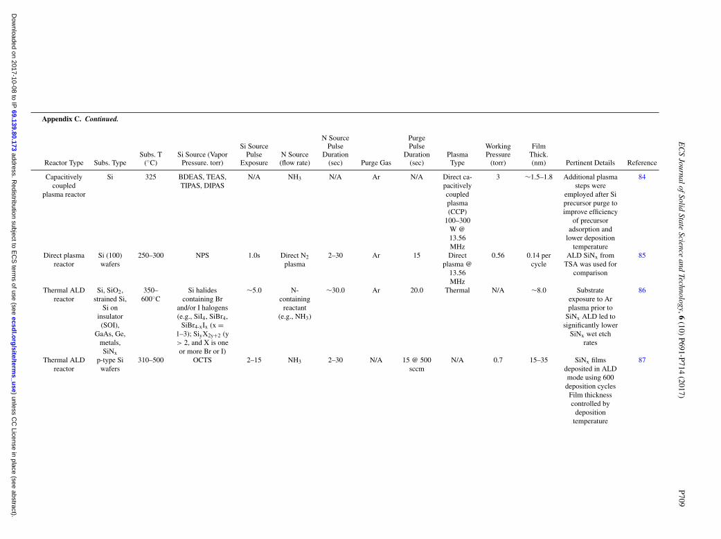
EC
SJournalofSolid
StateScience
andTechnology,6
(10)P691-P714
(2017)P709
Appendix C. Continued.
Reactor Type Subs. TypeSubs. T
(◦C)Si Source (Vapor
Pressure. torr)
Si SourcePulse
ExposureN Source(flow rate)
N SourcePulse
Duration(sec) Purge Gas
PurgePulse
Duration(sec)
PlasmaType
WorkingPressure
(torr)
FilmThick.(nm) Pertinent Details Reference
Capacitivelycoupled
plasma reactor
Si 325 BDEAS, TEAS,TIPAS, DIPAS
N/A NH3 N/A Ar N/A Direct ca-pacitivelycoupledplasma(CCP)
100–300W @13.56MHz
3 ∼1.5–1.8 Additional plasmasteps were
employed after Siprecursor purge toimprove efficiency
of precursoradsorption and
lower depositiontemperature
84
Direct plasmareactor
Si (100)wafers
250–300 NPS 1.0s Direct N2plasma
2–30 Ar 15 Directplasma @
13.56MHz
0.56 0.14 percycle
ALD SiNx fromTSA was used for
comparison
85
Thermal ALDreactor
Si, SiO2,strained Si,
Si oninsulator(SOI),
GaAs, Ge,metals,SiNx
350–600◦C
Si halidescontaining Br
and/or I halogens(e.g., SiI4, SiBr4,
SiBr4-xIx (x =1–3); SiyX2y+2 (y> 2, and X is oneor more Br or I)
∼5.0 N-containing
reactant(e.g., NH3)
∼30.0 Ar 20.0 Thermal N/A ∼8.0 Substrateexposure to Arplasma prior to
SiNx ALD led tosignificantly lower
SiNx wet etchrates
86
Thermal ALDreactor
p-type Siwafers
310–500 OCTS 2–15 NH3 2–30 N/A 15 @ 500sccm
N/A 0.7 15–35 SiNx filmsdeposited in ALDmode using 600
deposition cyclesFilm thicknesscontrolled by
depositiontemperature
87
) unless CC
License in place (see abstract). ecsd
l.org
/site/terms_u
se address. R
edistribution subject to EC
S term
s of use (see 69.139.80.173
Dow
nloaded on 2017-10-08 to IP

P710E
CS
JournalofSolidState
Scienceand
Technology,6(10)
P691-P714(2017)
Appendix C. Continued.
ReactorType Subs. Type
Subs. T(◦C)
Si Source (VaporPressure. torr)
Si SourcePulse
ExposureN Source(flow rate)
N SourcePulse
Duration(sec) Purge Gas
PurgePulse
Duration(sec)
PlasmaType
WorkingPressure
(torr)
FilmThick.(nm) Pertinent Details Reference
RemotePA-ALDreactor
ZnSeinternal
reflectioncrystal(IRC)
350–450 HCDS 5–30 NH3plasma
5–45 Ar 30 @ 100sccm
NH3 0.7–1 30 Surface reactionsduring Si2Cl6 and
NH3 plasmahalf-cycles wereobserved using in
situ attenuatedtotal reflection
FTIR to identifysurface reactive
sites, andelucidate H
incorporationmechanism in
SiNx
88
RemotePA-ALDreactor
c-Si withthin oxide
layer
R.T.-500 BTBAS 0.15–3.0 N2 10 Ar 1 @ 100sccm
RemoteICP
plasma600 W @
13.56MHz
10−6 N/A Propertiesdependent on
plasma exposuretime, pressure and
substratetemperature
89
RemotePA-ALDreactor
N/A N/A BTBAS N/A NH3 or N2H2 + N2plasma
N/A N/A N/A N/A N/A N/A Comparison of theeffects of NH3,N2, or H2 + N2plasma on SiNx
growth rates
90
RemotePlasmareactor
c-Si withthin oxide
layer
80–200 BTBAS 0.15–3.0 N2 10 Ar RemoteICP
plasma600 W @
13.56MHz
0.8 10 Thin films of SiNxdeposited at low
temperatures
91
RemotePA-ALDreactor
N/A 200–400 BTBAS 0.15–3.0 N2 10 Ar 10 @ 100sccm
RemoteICP
plasma600 W @
13.56MHz
0.2–0.4 Re-depositioncontrolled by gas
residence timeduring the plasma
step
89
) unless CC
License in place (see abstract). ecsd
l.org
/site/terms_u
se address. R
edistribution subject to EC
S term
s of use (see 69.139.80.173
Dow
nloaded on 2017-10-08 to IP

EC
SJournalofSolid
StateScience
andTechnology,6
(10)P691-P714
(2017)P711
Appendix C. Continued.
ReactorType Subs. Type
Subs. T(◦C) Si Source (Vapor Pressure. torr)
Si SourcePulse
ExposureN Source(flow rate)
N SourcePulse
Duration(sec)
PurgeGas
PurgePulse
Duration(sec) Plasma Type
WorkingPressure
(torr)
FilmThick.(nm) Pertinent Details Reference
Directplasmareactor
Poly-Si/TiN/HfO2
stacks
400 or500
DCS, MCS N/A IonizedNH3
N/A N/A N/A Directplasma
N/A <5 nm DCS used for SiNxfor gate encapsulationapplications @500◦C;
MCS used for SiNxfor spacer
applications @400◦C
93
RemotePA-ALDreactor
p-type Si(100)
50–400 TSA @ 12◦C (315 torr @R.T.) 0.2 NH3 5 Ar 15 Remoteplasma
0.3 4–25 SiNx thin filmcharacteristics
controlled by dep.temp. to adjust thedefect density forcharge trap flash
memory applications
94
ThermalALD
reactor
Bareβ-Si3N4surface
N/A BDEAS, BTBAS N/A NH3 N/A N/A N/A N/A N/A N/A First principles studyusing density
functional theory tomodel the growth of aSi3N4 surface in a full
ALD cycle
95
Thermal orplasmaALD
reactor
(100)double-sided
Si
450 Dialkylamide silanes withformula SiH2 (NR′ R′′)2
including:SiH2DMA2[R=R′′=CH3];bis-(dimethylamino)silane,
SiH2HFMA2 [R=R′′=CF3];bis-(hexa-
fluorodimethylamino)silane],SiH2EMA2
[R′=CH3,R′′+=CH2CH3];bis(ethylmethylamino)silane],BDEAS, BTBAS, SiH2(NH2)2
(diaminosilane); and DIPASSiH2Cl2 (dichlorosilane);
SiH2(CH3)2 (dimethylsilane)and SiH4
∼1.0–8.0torr.sec
NH3 N/A N/A N/A N/A N/A N/A First-principlesdensity functional
theory to probedifferences betweenALD O2 and Si3N4
using varioustheoretical
approaches, includingmodel reaction
pathways,acidity/basicity of the
oxide vs nitridesurfaces and overall
energetics as afunction of precursor
functional group
96
) unless CC
License in place (see abstract). ecsd
l.org
/site/terms_u
se address. R
edistribution subject to EC
S term
s of use (see 69.139.80.173
Dow
nloaded on 2017-10-08 to IP

P712E
CS
JournalofSolidState
Scienceand
Technology,6(10)
P691-P714(2017)
Appendix C. Continued.
ReactorType Subs. Type
Subs. T(◦C) Si Source (Vapor Pressure. torr)
Si SourcePulse
ExposureN Source(flow rate)
N SourcePulse
DurationPurgeGas
PurgePulse
Duration(sec) Plasma Type
WorkingPressure
(torr)
FilmThick.(nm) Pertinent Details Reference
Thermal orPE-ALDreactor
Sistructures
400 Si precursors containing aniodine ligand such as HSiI3,
H2SiI2, H3SiI, H2Si2I4,H4Si2I2, H5Si2I)
0.05–5.0 NH3,N2H4, N2
0.1–10 N2, Aror He
0.1–10 Remote ordirect
plasma@10–1000
W
N/A N/A SiNx films exhibitedetch rates in dilutedHF that were half of
those for SiO2
101
Parallel–plate ca-pacitancePE-ALDreactor
(100)double-sided
polished Siwith nativeSiO2 layer
400 SiH4 0.0–15.0 N2 0.5–90 N2 1–5 Lowfrequency
(LF)(200–400kHz) and
highfrequency
(HF) (13.56MHz) power
sources
2.5 ∼0.5–90 PEALD SiNx:Hgrowth was performed
both on native SiO2and on 25 nm PECVD
SiNx:H and SiO2films previously
deposited on nativeoxide of the Si
substrate
11
PE-ALDreactor
SiO2substrates
270◦C TIPAS 0.5–2.0 NH3 8.0 Ar 10.0 Direct 13.56MHz plasma
@100W
3 PE-ALD SiNx waspart of formingRuSiNx films as
diffusion barrier forCu interconnects
97,98
Thermal intraveling-wave-typecold-wallreactor)
B-dopedSi (100)wafers
∼515–573◦C
HCDS 0.1–3.0 ×10⁸L
NH3 1.0–10 ×108L
Ar N/A No plasma 1 torrand 10
torr
20 SiNx films werenonstoichiometric andeasily oxidized by airexposure to contain
7–8 at.% oxygen
117
∗For full descriptions of Si source acronyms used in this Appendix, see Table V.
) unless CC
License in place (see abstract). ecsd
l.org
/site/terms_u
se address. R
edistribution subject to EC
S term
s of use (see 69.139.80.173
Dow
nloaded on 2017-10-08 to IP

ECS Journal of Solid State Science and Technology, 6 (10) P691-P714 (2017) P713
References
1. W. Daves, A. Krauss, N. Behnel, V. Haublein, A. Bauer, and L. Frey, Thin SolidFilms, 519(18), 5892 (2011).
2. P. Kouakou, M. Belmahi, V. Brien, V. Hody, H. N. Migeon, and J. Bougdira, Surf.Coat. Technol., 203(3–4), 277 (2008).
3. A. S. Bhattacharyya and S. K. Mishra, J. Raman Spectrosc., 41(10), 1234 (2010).4. V. I. Ivashchenko, A. O. Kozak, O. K. Porada, L. A. Ivashchenko,
O. K. Sinelnichenko, O. S. Lytvyn, T. V. Tomila, and V. J. Malakhov, ThinSolid Films, 569, 57 (2014).
5. T. Lube and J. Dusza, J. Eur. Ceram. Soc., 27(2–3), 1203 (2007).6. H. Matsumura, Japanese J. Appl. Physics, Part 1 Regul. Pap. Short Notes Rev. Pap.,
37(6 A), 3175 (1998).7. N. I. Fainer and V. I. Kosyakov, J. Struct. Chem., 56(1), 163 (2015).8. C. Zhuang, R. Fuchs, C. Schlemper, T. Staedler, and X. Jiang, Thin Solid Films,
592, 167 (2015).9. Y. Awad, M. A. El Khakani, C. Aktik, J. Mouine, N. Camire, M. Lessard, and
M. Scarlete, Mater. Chem. Phys., 104(2–3), 350 (2007).10. E. Graef, B. Huizing, and R. Mahnkopf, International Technology Roadmap for
Semiconductors 2.0, 2015th ed., 2015.11. S. W. King, J. Vac. Sci. Technol. A, 29(4), 41501 (2011).12. S. W. King, ECS J. Solid State Sci. Technol., 4(1), N3029 (2014).13. X. Meng, Y. -C. Byun, H. Kim, J. Lee, A. Lucero, L. Cheng, and J. Kim, Materials
(Basel)., 9(12), 1007 (2016).14. T. Usami, T. Ide, Y. Kakuhara, Y. Ajima, K. Ueno, T. Maruyama, Y. Yu, E. Apen,
K. Chattopadhyay, B. Van Schravendijk, N. Oda, and M. Sekine, In 2006 Interna-tional Interconnect Technology Conference, IITC; IEEE, 2006; pp 125.
15. Y. Kuo, Vacuum, 51(4), 741 (1998).16. J. Yota, ECS Trans., 35(4), 229 (2011).17. W. Liao, X. Zeng, W. Yao, and X. Wen, Appl. Surf. Sci., 351, 1053 (2015).18. T. Stapinski and B. Swatowska, J. Electron. Mater., 37(6), 905 (2008).19. Z. Khatami, P. R. J. Wilson, J. Wojcik, and P. Mascher, Thin Solid Films, 622, 1
(2017).20. S. Majee, M. F. Cerqueira, D. Tondelier, J. C. Vanel, B. Geffroy, Y. Bonnassieux,
P. Alpuim, and J. E. Bouree, Thin Solid Films, 575, 72 (2015).21. P. Alpuim, S. Majee, M. F. Cerqueira, D. Tondelier, B. Geffroy, Y. Bonnassieux,
and J. E. Bouree, Thin Solid Films, 595, 258 (2015).22. S. Ueno, Y. Konishi, and K. Azuma, Thin Solid Films, 580, 116 (2015).23. K. Azuma, S. Ueno, Y. Konishi, and K. Takahashi, Thin Solid Films, 580, 111
(2015).24. M. Smietana, W. J. Bock, and J. Szmidt, Thin Solid Films, 519(19), 6339 (2011).25. M. B. Takeyama, M. Sato, Y. Nakata, Y. Kobayashi, T. Nakamura, and A. Noya,
Jpn. J. Appl. Phys., 53, 19 (2014).26. J. S. Lee, B. B. Sahu, and J. G. Han, Phys. Chem. Chem. Phys., 18(47), 32198
(2016).27. N. Tabassum, V. Nikas, B. Ford, M. Huang, A. E. Kaloyeros, and S. Gallis, Appl.
Phys. Lett., 109(4), 43104 (2016).28. V. Nikas, N. Tabassum, B. Ford, L. Smith, A. E. Kaloyeros, and S. Gallis, J. Mater.
Res., (30), 1 (2015).29. S. Gallis, V. Nikas, E. Eisenbraun, M. Huang, and A. E. Kaloyeros, J. Mater. Res.,
24(8), 2561 (2009).30. S. Gallis, M. Huang, and A. E. Kaloyeros, Appl. Phys. Lett., 90(16), 161914 (2007).31. Y. H. So, S. Huang, G. Conibeer, and M. A. Green, Thin Solid Films, 519(16), 5408
(2011).32. T. V. Torchynska, J. L. Casas Espinola, E. Vergara Hernandez, L. Khomenkova,
F. Delachat, and A. Slaoui, Thin Solid Films, 581, 65 (2015).33. L. Wang, H. Qin, W. Zhang, L. Zhang, and D. Yan, Thin Solid Films, 545, 514
(2013).34. A. Ahnood, Y. Suzuki, A. Madan, and A. Nathan, Thin Solid Films, 520(15), 4831
(2012).35. T. Chen, Y. Huang, D. Yang, R. Carius, and F. Finger, Thin Solid Films, 519(14),
4523 (2011).36. J. M. Kopfer, S. Keipert-Colberg, and D. Borchert, Thin Solid Films, 519(19), 6525
(2011).37. M. S. Bailly, J. Karas, H. Jain, W. J. Dauksher, and S. Bowden, Thin Solid Films,
612, 243 (2016).38. A. S. Keita, A. En Naciri, F. Delachat, M. Carrada, G. Ferblantier, A. Slaoui, and
M. Stchakovsky, Thin Solid Films, 519(9), 2870 (2011).39. J. Wei, P. L. Ong, F. E. H. Tay, and C. Iliescu, Thin Solid Films, 516(16), 5181
(2008).40. D. Fine, A. Grattoni, R. Goodall, S. S. Bansal, C. Chiappini, S. Hosali,
A. L. van de Ven, S. Srinivasan, X. Liu, B. Godin, L. Brousseau, I. K. Yazdi,J. Fernandez-Moure, E. Tasciotti, H. J. Wu, Y. Hu, S. Klemm, and M. Ferrari,Adv. Healthc. Mater., 2(5), 632 (2013).
41. J. M. Maloney, S. A. Lipka, S. P. Baldwin, H. Hammerle, K. Kobuch, K. Kohler,W. Nisch, H. Sachs, M. Stelzle, Y. Li, R. S. Shawgo, B. Tyler, P. T. Henderson,J. S. Vogel, A. Rosenberg, P. B. Storm, R. Langer, H. Brem, M. J. Cima, D. J. Edell,J. W. Osenbach, M. Vogt, R. Hauptmann, G. Schmitt, J. -W. Schultze, F. Faßbender,G. Buß, H. Luth, and M. Schoning, MRS Online Proc. Libr. Arch., 872(3), 797(2005).
42. G. Kotzar, M. Freas, P. Abel, A. Fleischman, S. Roy, C. Zorman, J. M. Moran, andJ. Melzak, Biomaterials, 23(13), 2737 (2002).
43. A. Neumann, T. Reske, M. Held, K. Jahnke, C. Rago, and H. R. Maier, J. Mater.Sci. Mater. Med., 15(10), 1135 (2004).
44. C. C. Guedes E Silva, B. Konig, M. J. Carbonari, M. Yoshimoto, S. Allegrini, andJ. C. Bressiani, J. Biomed. Mater. Res. - Part A, 84(2), 337 (2008).
45. T. J. Webster, A. A. Patel, M. N. Rahaman, and B. Sonny Bal, Acta Biomater., 8(12),4447 (2012).
46. M. R. Badaruddin, M. R. Muhamad, and S. A. Rahman, Thin Solid Films, 519(15),5082 (2011).
47. M. Belmahi, S. Bulou, A. Thouvenin, L. De Poucques, R. Hugon, L. Le Brizoual,P. Miska, D. Geneve, J. L. Vasseur, and J. Bougdira, Plasma Process. Polym., 11(6),551 (2014).
48. Z. Ma, J. Zhou, Z. Chen, and E. Xie, Diam. Relat. Mater., 20(4), 475 (2011).49. S. Bulou, L. Brizoual, P. Le Miska, L. Poucques, R. de Hugon, and M. Belmahi,
IOP Conf. Ser. Mater. Sci. Eng., 12(1), 12002 (2010).50. A. K. Sinha and E. Lugujjo, Appl. Phys. Lett., 32(4), 245 (1978).51. E. F. Krimmel and R. Hezel, Silicon Nitride in Microelectronics and Solar Cells
(Gmelin Si B 5c), A. Peble and F. Schroder, Eds., Springer Berlin Heidelberg:Berlin, Heidelberg, 1991.
52. F. I. Riley, J. Am. Ceram. Soc., 83(2), 245 (2000).53. S. Hampshire, J. Achiev. Mater. Manuf. Eng., 24(1), 43 (2007).54. G. Ziegler, J. Heinrich, and G. Wotting, J. Mater. Sci., 22(9), 3041 (1987).55. Y. Kaga, H. Imamura, and J. Watanabe, Silicon nitride substrate manufacturing
method, silicon nitride substrate, silicon nitride circuit substrate, and semiconductormodule. 8,858,865, (2014).
56. M. Weinmann, In Inorganic Polymers, R. Jaeger M. De Gleria, Eds., Nova SciencePublishers, 2007; pp 371.
57. G. Mera, M. Gallei, S. Bernard, and E. Ionescu, Nanomaterials, 5(2), 468(2015).
58. E. Kroke, Y. Li, C. Konetschny, E. Lecomte, C. Fasel, and R. Riedel, Mater. Sci.Eng. R Reports, 26(4–6), 97 (2000).
59. A. L. Hector, Coord. Chem. Rev., 323, 120 (2016).60. G. Barroso, Q. Li, G. Motz, and R. K. Bordia, Am. Ceram. Soc. Bull., 96(3), 42
(2017).61. D. Seyferth and G. H. Wiseman, J. Am. Ceram. Soc., 67(7), C132 (1984).62. B. Arkles, J. Electrochem. Soc., 133(1), 233 (1986).63. L. A. Liew, W. Zhang, V. M. Bright, L. An, M. L. Dunn, and R. Raj, Sensors
Actuators, A Phys., 89(1–2), 64 (2001).64. A. Lukacs, Am. Ceram. Soc. Bull., 86(1), 9301 (2007).65. N. Shinde, Y. Takano, J. Sagan, V. Monreal, and T. Nagahara, J. Photopolym. Sci.
Technol., 23(2), 225 (2010).66. T. Isoda, H. Kaya, H. Nishii, O. Funayama, T. Suzuki, and Y. Tashiro, J. Inorg.
Organomet. Polym., 2(1), 151 (1992).67. J. H. Lee, J. H. Cho, J. S. Choi, and D. Lee, Spin-on glass composition and method
of forming silicon oxide layer in semiconductor manufacturing process using thesame. US20040224537 A1, (2004).
68. B. C. Arkles, Y. Pan, and F. Jove, Hydridosilapyrroles, hydridosilaazapyrroles, thi-asilacyclopentanes, method for preparation thereof, and reaction products therefrom.WO2016205073 A1, (2016).
69. A. Markwitz, H. Baumann, E. Krimmel, M. Rose, K. Bethge, P. Misaelides, andS. Logothetidis, Vacuum, 44(3–4), 367 (1993).
70. B. Arkles, Y. Pan, and A. E. Kaloyeros, Electrochem. Soc. Trans., 64(9), 243(2014).
71. L. Ju, N. C. Strandwitz, and M. Green, J. Mater. Chem. C, 4(18), 4034 (2016).72. S. M. George, Chem. Rev., 110(1), 111 (2010).73. E. Eisenbraun, A. Upham, R. Dash, W. Zeng, J. Hoefnagels, S. Lane, D. Anjum,
K. Dovidenko, A. Kaloyeros, B. Arkles, and J. J. Sullivan, J. Vac. Sci. Technol. BMicroelectron. Nanom. Struct., 18(4), 2011 (2000).
74. D. Dergez, M. Schneider, A. Bittner, and U. Schmid, Thin Solid Films, 589, 227(2015).
75. L. Khomenkova, P. Normand, F. Gourbilleau, A. Slaoui, and C. Bonafos, Thin SolidFilms, 617, 143 (2016).
76. M. Smietana, M. Dominik, M. Mysliwiec, N. Kwietniewski, P. Mikulic,B. S. Witkowski, and W. J. Bock, Thin Solid Films, 603, 8 (2016).
77. K. Kobayashi, A. Suzuki, and K. Ishikawa, Thin Solid Films, 550, 545 (2014).78. D. Li, T. Kunz, N. Wolf, J. P. Liebig, S. Wittmann, T. Ahmad, M. T. Hessmann,
R. Auer, M. Goken, and C. J. Brabec, Thin Solid Films, 583(1), 25 (2015).79. F. J. H. Van Assche, S. Unnikrishnan, J. J. Michels, A. M. B. Van Mol,
P. Van De Weijer, M. C. M. Van De Sanden, and M. Creatore, Thin Solid Films,558, 54 (2014).
80. Y. Kim, J. Provine, S. P. Walch, J. Park, W. Phuthong, A. L. Dadlani, H. J. Kim,P. Schindler, K. Kim, and F. B. Prinz, ACS Appl. Mater. Interfaces, 8(27), 17599(2016).
81. J. Provine, P. Schindler, Y. Kim, S. P. Walch, H. J. Kim, K. H. Kim, and F. B. Prinz,AIP Adv., 6(6) (2016).
82. L. L. Yusup, J.-M. Park, Y.-H. Noh, S.-J. Kim, W.-J. Lee, S. Park, and Y.-K. Kwon,RSC Adv., 6(72), 68515 (2016).
83. J.-M. Park, S. J. Jang, L. L. Yusup, W.-J. Lee, and S.-I. Lee, ACS Appl. Mater.Interfaces, 8(32), 20865 (2016).
84. S. Suh, S. W. Ryu, S. Cho, J.-R. Kim, S. Kim, C. S. Hwang, and H. J. Kim, J. Vac.Sci. Technol. A Vacuum, Surfaces, Film., 34(1), 01A136 (2016).
85. S. Weeks, G. Nowling, N. Fuchigami, M. Bowes, and K. Littau, J. Vac. Sci. Technol.A Vacuum, Surfaces, Film., 34(1), 01A140 (2016).
86. M. Saly, Deposition Of Si-H Free Silicon Nitride. US20160307748 A1, (2016).87. S. Riedel, J. Sundqvist, and T. Gumprecht, Thin Solid Films, 577, 114 (2015).88. R. a. Ovanesyan, D. M. Hausmann, and S. Agarwal, ACS Appl. Mater. Interfaces,
7(20), 10806 (2015).89. H. C. M. Knoops, E. M. J. Braeken, K. de Peuter, S. E. Potts, S. Haukka, V. Pore,
and W. M. M. Kessels, ACS Appl. Mater. Interfaces, 7(35), 19857 (2015).90. C. K. Ande, H. C. M. Knoops, K. de Peuter, M. van Drunen, S. D. Elliott, and
W. M. M. Kessels, J. Phys. Chem. Lett., 6(18), 3610 (2015).
) unless CC License in place (see abstract). ecsdl.org/site/terms_use address. Redistribution subject to ECS terms of use (see 69.139.80.173Downloaded on 2017-10-08 to IP

P714 ECS Journal of Solid State Science and Technology, 6 (10) P691-P714 (2017)
91. A. M. Andringa, A. Perrotta, K. De Peuter, H. C. M. Knoops, W. M. M. Kessels,and M. Creatore, ACS Appl. Mater. Interfaces, 7(40), 22525 (2015).
92. H. C. M. Knoops, K. De Peuter, and W. M. M. Kessels, Appl. Phys. Lett., 107(1)(2015).
93. F. Koehler, D. H. Triyoso, I. Hussain, B. Antonioli, and K. Hempel, Phys. StatusSolidi Curr. Top. Solid State Phys., 11(1), 73 (2014).
94. W. Jang, H. Jeon, C. Kang, H. Song, J. Park, H. Kim, H. Seo, M. Leskela, andH. Jeon, Phys. Status Solidi, 211(9), 2166 (2014).
95. L. Huang, B. Han, B. Han, A. Derecskei-Kovacs, M. Xiao, X. Lei, M. L. O’Neill,R. M. Pearlstein, H. Chandra, and H. Cheng, Phys. Chem. Chem. Phys., 16(34),18501 (2014).
96. C. A. Murray, S. D. Elliott, D. Hausmann, J. Henri, and A. LaVoie, ACS Appl. Mater.Interfaces, 6, 10534 (2014).
97. T.-K. Eom, S.-H. Kim, D.-H. Kang, and H. Kim, J. Electrochem. Soc., 158(11),D657 (2011).
98. T.-K. Eom, S.-H. Kim, K.-S. Park, S. Kim, and H. Kim, Electrochem. Solid-StateLett., 14(1), D10 (2011).
99. K. Park, W. D. Yun, B. J. Choi, H. Kim, W. J. Do Lee, S. K. Rha, and C. O. Park,Thin Solid Films, 517(14), 3975 (2009).
100. T. Saito, T. Nishizawa, Y. Kinoshita, and N. Nashida, Electronic component andmanufacturing method for electronic component. US Pat. 9355987, (2016).
101. A. J. Niskanen, S. Chen, V. Pore, A. Fukazawa, and H. Fukuda, Si Precurosors forDeposition of SiN at Low Temperatures. US20140273531 A1, (2014).
102. R. Walsh, In Silicon Compounds: Silanes and Silicones, B. Arkles and G. L. Larson,Eds., 2008; pp 200.
103. J. A. Pople and L. A. Curtiss, J. Chem. Phys., 95(6), 4385 (1991).104. B. Arkles and G. L. Larson, Silicon Compounds: Silanes and Silicones, 4th ed.,
2013.105. B. C. Arkles and A. E. Kaloyeros, Silicon based films formed from iodosilane
precursors and method of making the same. US Pat. 6586056, (2003).106. X. Lin, D. Endisch, X. Chen, and A. Kaloyeros, MRS Proc., 495, 107 (1997).107. L. -Q. Xia and M. In Chang, Handbook of Semiconductor Manufacturing Technol-
ogy, CRC Press, 2008; pp 13-1-13–87.108. S. Koseki and A. Ishitani, J. Appl. Phys., 72(12), 5808 (1992).109. D. L. Smith, A. S. Alimonda, and F. J. von Preissig, J. Electrochem. Soc., 8(3), 551
(1990).110. D. L. Smith, A. S. Alimonda, C. Chen, S. E. Ready, and B. Wacker, J. Electrochem.
Soc., 137(2), 614 (1990).111. J. W. Smith, S. M. Seutter, and R. S. Iyer, J. Electrochem. Soc., 152(4), G316 (2005).112. Y. Wu, H. Zhong, J. Romero, C. Tabery, C. Cheung, B. MacDonald, J. Bhakta,
A. Halliyal, F. Cheung, and R. Ogle, J. Electrochem. Soc., 150(12), G785(2003).
113. M. Tanaka, S. Saida, and Y. Tsunashima, J. Electrochem. Soc., 147(6), 2284 (2000).114. K. E. Bean, P. S. Gleim, R. L. Yeakley, and W. R. Runyan, J. Electrochem. Soc.,
114(7), 733 (1967).115. S. M. Hu, J. Electrochem. Soc., 113(7), 693 (1966).116. D. Dergez, M. Schneider, A. Bittner, N. Pawlak, and U. Schmid, Thin Solid Films,
606, 7 (2016).117. K. Park, W. D. Yun, B. J. Choi, H. Kim, W. J. Do Lee, S. K. Rha, and C. O. Park,
Thin Solid Films, 517(14), 3975 (2009).118. L. Huang, B. Han, M. Fan, and H. Cheng, RSC Adv., 7(37), 22672 (2017).119. L. Wang, R. W. Snidle, and L. Gu, Wear., 159 (2000).120. S. Schmidt, T. Hanninen, C. Goyenola, J. Wissting, J. Jensen, L. Hultman,
N. Goebbels, M. Tobler, and H. Hogberg, ACS Appl. Mater. Interfaces, 8(31),20385 (2016).
121. T. Serikawa and A. Okamoto, J. Electrochem. Soc., 131(12), 2928 (1984).122. B. C. Joshi, G. Eranna, D. P. Runthala, B. B. Dixit, O. P. Wadhawan, and P. D. Vyas,
Indian J. Eng. Mater. Sci., 7(5–6), 303 (2000).123. T. S. Hickernell, F. M. Fliegel, and F. S. Hickernell, IEEE Symp. Ultrason., 445
(1990).124. M. Maeda and Y. Arita, J. Appl. Phys., , 53(10), 6852 (1982).125. G. Carlotti, P. Colpani, D. Piccolo, S. Santucci, V. Senez, G. Socino, and L. Verdini,
Thin Solid Films, 414(1), 99 (2002).126. F. S. Hickernell and T. S. Hickernell, IEEE Trans. Ultrason. Ferroelectr. Freq. Con-
trol, 42(3), 410 (1995).127. J. A. Taylor, J. Vac. Sci. Technol. A Vacuum, Surfaces, Film., 9(4), 2464 (1991).128. S. King, R. Chu, G. Xu, and J. Huening, Thin Solid Films, 518(17), 4898 (2010).129. S. W. King and J. A. Gradner, Microelectron. Reliab., 49(7), 721 (2009).130. J. J. Mei, H. Chen, W. Z. Shen, and H. F. W. Dekkers, J. Appl. Phys., 100(7), 73516
(2006).131. M. Vila, D. Caceres, and C. Prieto, J. Appl. Phys., 94(12), 7868 (2003).132. Y. Toivola, J. Thurn, R. F. Cook, G. Cibuzar, and K. Roberts, J. Appl. Phys., 94(10),
6915 (2003).133. Ferro-Ceramic Grinding Inc. Ceramic Silicon Nitride | Silicon Nitride Properties
http://www.ferroceramic.com/silicon_nitride.htm (accessed Aug 20, 2017).134. J. J. Vlassak and W. D. Nix, J. Mater. Res., 7(12), 3242 (1992).135. P. French, P. Sarro, R. Mallee, E. Fakkeldij, and R. Wolffenbuttel, Sensors Actuators
A Phys., 58(2), 149 (1997).136. T. Kramer and O. Paul, IEEE Sixt. Annu. Int. Conf. Micro Electro Mech. Syst., No.
Mml, 678 (2003).137. S. Hasegawa, Y. Amano, T. Inokuma, and Y. Kurata, J. Appl. Phys., 72(12), 5676
(1992).138. V. Ziebart, O. Paul, U. Munch, and H. Baltes, Mater. Res. Soc. Symp. - Proc., 505(V),
27 (1998).139. G. Ziegler, Mater. Sci. Forum, 47, 162 (1989).140. A. J. Eckel, NASA Research News, 2009, p https://web.archive.org/
web/20090404161958.141. C. H. Mastrangelo, Y. C. Tai, and R. S. Muller, Sensors Actuators A. Phys., 23(1–3),
856 (1990).142. S. Govorkov, W. Ruderman, M. W. Horn, R. B. Goodman, and M. Rothschild, Rev.
Sci. Instrum., 68(10), 3828 (1997).143. A. J. Griffin, F. R. Brotzen, and P. J. Loos, J. Appl. Phys., 76(7), 4007 (1994).144. R. Sultan, A. D. Avery, J. M. Underwood, S. J. Mason, D. Bassett, and B. L. Zink,
Phys. Rev. B, 87(21), 214305 (2013).145. S. -M. Lee and D. G. Cahill, J. Appl. Phys., 81(6), 2590 (1997).146. M. Bogner, A. Hofer, G. Benstetter, H. Gruber, and R. Y. Q. Fu, Thin Solid Films,
591, 267 (2015).147. A. Piccirillo and A. L. Gobbi, J. Electrochem. Soc., 137(12), 3910 (1990).148. I. Khan and M. Zulfequar, Mater. Sci. Appl., 2(July), 738 (2011).149. M. A. Signore, A. Sytchkova, D. Dimaio, A. Cappello, and A. Rizzo, Opt. Mater.
(Amst)., 34(4), 632 (2012).150. E. A. Davis, N. Piggins, and S. C. Bayliss, Solid State Phys., 20(27), 4415 (1987).151. A. J. Lowe, M. J. Powell, and S. R. Elliott, J. Appl. Phys., 59(4), 1251 (1986).152. H. Charifi, A. Slaoui, J. P. Stoquert, H. Chaib, A. Hannour, and H. Charifi, World J.
Condens. Matter Phys., 6(6), 7 (2016).153. R. C. Dante and C. K. Kajdas, Wear, 288, 27 (2012).154. P. F. Carcia, R. S. McLean, M. H. Reilly, M. D. Groner, and S. M. George, Appl.
Phys. Lett., 89(3), 31915 (2006).155. D. S. Wuu, W. C. Lo, C. C. Chiang, H. B. Lin, L. S. Chang, R. H. Horng,
C. L. Huang, and Y. J. Gao, Surf. Coatings Technol., 197(2–3), 253 (2005).
) unless CC License in place (see abstract). ecsdl.org/site/terms_use address. Redistribution subject to ECS terms of use (see 69.139.80.173Downloaded on 2017-10-08 to IP


![Structure and composition of silicon nitride and silicon ...688638/FULLTEXT02.pdf · Silicon nitride is currently being introduced as a biomaterial [14-22]. A product based on silicon](https://static.fdocuments.net/doc/165x107/5f0845fa7e708231d4213187/structure-and-composition-of-silicon-nitride-and-silicon-688638fulltext02pdf.jpg)