Review - Technion Faculty of Electrical Engineeringwebee.technion.ac.il/.../FET_Review.pdf · ·...
18
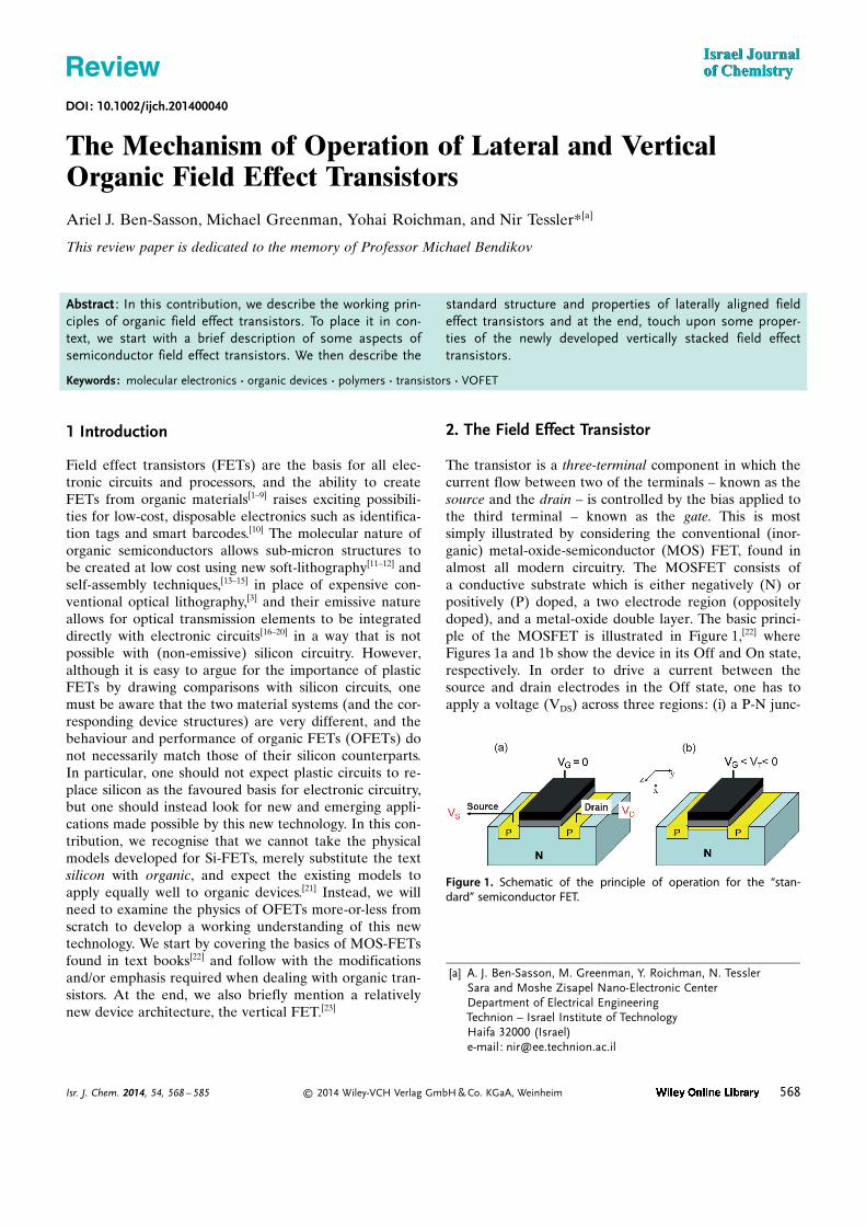
DOI: 10.1002/ijch.201400040 The Mechanism of Operation of Lateral and Vertical Organic Field Effect Transistors ArielJ. Ben-Sasson, Michael Greenman, Yohai Roichman, and Nir Tessler* [a] This review paper is dedicated to the memory of Professor Michael Bendikov 1 Introduction Field effect transistors (FETs) are the basis for all elec- tronic circuits and processors, and the ability to create FETs from organic materials [1–9] raises exciting possibili- ties for low-cost, disposable electronics such as identifica- tion tags and smart barcodes. [10] The molecular nature of organic semiconductors allows sub-micron structures to be created at low cost using new soft-lithography [11–12] and self-assembly techniques, [13–15] in place of expensive con- ventional optical lithography, [3] and their emissive nature allows for optical transmission elements to be integrated directly with electronic circuits [16–20] in a way that is not possible with (non-emissive) silicon circuitry. However, although it is easy to argue for the importance of plastic FETs by drawing comparisons with silicon circuits, one must be aware that the two material systems (and the cor- responding device structures) are very different, and the behaviour and performance of organic FETs (OFETs) do not necessarily match those of their silicon counterparts. In particular, one should not expect plastic circuits to re- place silicon as the favoured basis for electronic circuitry, but one should instead look for new and emerging appli- cations made possible by this new technology. In this con- tribution, we recognise that we cannot take the physical models developed for Si-FETs, merely substitute the text silicon with organic, and expect the existing models to apply equally well to organic devices. [21] Instead, we will need to examine the physics of OFETs more-or-less from scratch to develop a working understanding of this new technology. We start by covering the basics of MOS-FETs found in text books [22] and follow with the modifications and/or emphasis required when dealing with organic tran- sistors. At the end, we also briefly mention a relatively new device architecture, the vertical FET. [23] 2. The Field Effect Transistor The transistor is a three-terminal component in which the current flow between two of the terminals – known as the source and the drain – is controlled by the bias applied to the third terminal – known as the gate. This is most simply illustrated by considering the conventional (inor- ganic) metal-oxide-semiconductor (MOS) FET, found in almost all modern circuitry. The MOSFET consists of a conductive substrate which is either negatively (N) or positively (P) doped, a two electrode region (oppositely doped), and a metal-oxide double layer. The basic princi- ple of the MOSFET is illustrated in Figure 1, [22] where Figures 1a and 1b show the device in its Off and On state, respectively. In order to drive a current between the source and drain electrodes in the Off state, one has to apply a voltage (V DS ) across three regions: (i) a P-N junc- Abstract : In this contribution, we describe the working prin- ciples of organic field effect transistors. To place it in con- text, we start with a brief description of some aspects of semiconductor field effect transistors. We then describe the standard structure and properties of laterally aligned field effect transistors and at the end, touch upon some proper- ties of the newly developed vertically stacked field effect transistors. Keywords: molecular electronics · organic devices · polymers · transistors · VOFET Figure 1. Schematic of the principle of operation for the “stan- dard” semiconductor FET. [a] A.J. Ben-Sasson, M. Greenman, Y. Roichman, N. Tessler Sara and Moshe Zisapel Nano-Electronic Center Department of Electrical Engineering Technion – Israel Institute of Technology Haifa 32000 (Israel) e-mail: [email protected] Isr. J. Chem. 2014, 54, 568 – 585 # 2014 Wiley-VCH Verlag GmbH & Co. KGaA, Weinheim 568 Review
Transcript of Review - Technion Faculty of Electrical Engineeringwebee.technion.ac.il/.../FET_Review.pdf · ·...
DOI: 10.1002/ijch.201400040
The Mechanism of Operation of Lateral and VerticalOrganic Field Effect TransistorsAriel J. Ben-Sasson, Michael Greenman, Yohai Roichman, and Nir Tessler*[a]
This review paper is dedicated to the memory of Professor Michael Bendikov
1 Introduction
Field effect transistors (FETs) are the basis for all elec-tronic circuits and processors, and the ability to createFETs from organic materials[1–9] raises exciting possibili-ties for low-cost, disposable electronics such as identifica-tion tags and smart barcodes.[10] The molecular nature oforganic semiconductors allows sub-micron structures tobe created at low cost using new soft-lithography[11–12] andself-assembly techniques,[13–15] in place of expensive con-ventional optical lithography,[3] and their emissive natureallows for optical transmission elements to be integrateddirectly with electronic circuits[16–20] in a way that is notpossible with (non-emissive) silicon circuitry. However,although it is easy to argue for the importance of plasticFETs by drawing comparisons with silicon circuits, onemust be aware that the two material systems (and the cor-responding device structures) are very different, and thebehaviour and performance of organic FETs (OFETs) donot necessarily match those of their silicon counterparts.In particular, one should not expect plastic circuits to re-place silicon as the favoured basis for electronic circuitry,but one should instead look for new and emerging appli-cations made possible by this new technology. In this con-tribution, we recognise that we cannot take the physicalmodels developed for Si-FETs, merely substitute the textsilicon with organic, and expect the existing models toapply equally well to organic devices.[21] Instead, we willneed to examine the physics of OFETs more-or-less fromscratch to develop a working understanding of this newtechnology. We start by covering the basics of MOS-FETsfound in text books[22] and follow with the modificationsand/or emphasis required when dealing with organic tran-sistors. At the end, we also briefly mention a relativelynew device architecture, the vertical FET.[23]
2. The Field Effect Transistor
The transistor is a three-terminal component in which thecurrent flow between two of the terminals – known as thesource and the drain – is controlled by the bias applied tothe third terminal – known as the gate. This is mostsimply illustrated by considering the conventional (inor-ganic) metal-oxide-semiconductor (MOS) FET, found inalmost all modern circuitry. The MOSFET consists ofa conductive substrate which is either negatively (N) orpositively (P) doped, a two electrode region (oppositelydoped), and a metal-oxide double layer. The basic princi-ple of the MOSFET is illustrated in Figure 1,[22] whereFigures 1a and 1b show the device in its Off and On state,respectively. In order to drive a current between thesource and drain electrodes in the Off state, one has toapply a voltage (VDS) across three regions: (i) a P-N junc-
Abstract : In this contribution, we describe the working prin-ciples of organic field effect transistors. To place it in con-text, we start with a brief description of some aspects ofsemiconductor field effect transistors. We then describe the
standard structure and properties of laterally aligned fieldeffect transistors and at the end, touch upon some proper-ties of the newly developed vertically stacked field effecttransistors.
Keywords: molecular electronics · organic devices · polymers · transistors · VOFET
Figure 1. Schematic of the principle of operation for the “stan-dard” semiconductor FET.
[a] A. J. Ben-Sasson, M. Greenman, Y. Roichman, N. TesslerSara and Moshe Zisapel Nano-Electronic CenterDepartment of Electrical EngineeringTechnion – Israel Institute of TechnologyHaifa 32000 (Israel)e-mail: [email protected]
Isr. J. Chem. 2014, 54, 568 – 585 � 2014 Wiley-VCH Verlag GmbH & Co. KGaA, Weinheim 568
Review

tion; (ii) an N-doped bulk region; and (iii) an N-P junc-tion. In this case, one of the junctions is always orientedin the reverse direction to the applied field and hence,the current flowing through it is based on the negligibledensity of minority carriers (holes in N type region),making its value negligibly small. In the On state, a largenegative bias is applied to the gate electrode. The metallicgate, the oxide layer and the N-type bulk semiconductoract in effect as a capacitor, with the gate forming oneplate, the oxide acting as the dielectric spacer, and thesemiconductor forming the other plate. As with any ca-pacitor, if a bias is applied across the plates, opposite andequal charges will accumulate on the two plates. Hence,electrons accumulate at the gate and holes accumulate atthe oxide-semiconductor interface. If the bias applied tothe gate is sufficiently high, the interfacial hole densitywill be large enough to change the semiconductor fromN- to P-type. In this case, the current flowing through thereverse-bias diode is enhanced due to the high density ofholes in the N region; namely, current flows between thetwo P-type source and drain electrodes through the inter-mediate P-type layer (the channel).
The basic operation of organic FETs and MOSFETsare in many ways similar, although there are importantdifferences that arise from the different device structuresinvolved. In general, OFETs comprise three parts: (i)a metal or doped-organic conductor; (ii) an insulator; and(iii) a p-conjugated semiconductor. Hence, they can bedescribed as CIp-FETs and two typical CIp-FET struc-tures are shown in Figure 2. Notably, unlike theMOSFET of Figure 1, there is no P-N junction involvedand the source/drain electrodes are attached directly tothe p-conjugated semiconductor that makes up the chan-nel. Figures 2a and 2b represent two common CIp-FETarchitectures, named bottom and top contact configura-tion, respectively[24] . In the bottom contact configuration,the source/drain electrodes are in direct contact with theinsulator (and the channel), while in the top contact con-figuration, the source/drain electrodes are placed on theother side of the p-conjugated material.
Dr. Ariel J. Ben-Sasson holds a B.Sc. inbiomedical eng. (cum laude, 2005),and an M.Sc. and a Ph.D. in nano-science (2013) from Technion - IsraelInstitute of Technology. His Ph.D. in or-ganic electronics, supervised by Prof.Nir Tessler and Prof. Gitti Frey, focusedon the development of the novel verti-cal organic field effect transistor, itsblock-copolymer based self-assemblyfabrication methods, and underpinningphysical model. Ariel earned 8 awards,among which are the SPIE, EMRS,TSMC and Azrieli Fellowship. He is currently a postdoctoral fellowat Prof. David Baker’s lab, where he develops protein-engineeringtools aimed at introducing a molecular-design approach for pro-teins as smart materials.
Michael Greenman is in a direct Ph.D.program at the electrical engineeringfaculty in Technion. Michael’s main re-search is organic TFT’s, focusing onvertical organic field effect transistors.He also finished his bachelor degree inthe electrical engineering faculty inTechnion in 2011, specializing in nano-electronics and optoelectronics.
Dr. Yohai Roichman received his Ph.D.from Technion IIT, Electrical Engineer-ing department. In the following years,Yohai held research positions at Prince-ton University and New York University.Yohai’s research focused on chargetransport in organic semiconductors,statistical properties of transport out ofequilibrium systems, and holographicoptical trapping. Yohai has published30 peer review papers and 7 patents.Currently, Yohai is a private investor,founder of a technological and financialholding company.
Professor Nir Tessler received his B.Sc.summa cum laude from the ElectricalEngineering department, TechnionIsrael Institute of Technology in 1989.In 1995, he submitted his D.Sc. disser-tation on carrier dynamics in ultrafastIII-V lasers. In 1996, he published thefirst optically pumped conjugated poly-mer laser. After “falling in love” with or-ganic optoelectronics, he strived tocontribute to the understanding thatorganics can be used in numerous ap-plications. Nir is currently the head ofthe microelectronics and nanoelectronics research centres at theTechnion where he is trying to assist in areas outside his field of ex-pertise.
Figure 2. Schematic of an organic transistor based on conductor,insulator and p-conjugated material (CIp technology).
Isr. J. Chem. 2014, 54, 568 – 585 � 2014 Wiley-VCH Verlag GmbH & Co. KGaA, Weinheim www.ijc.wiley-vch.de 569
Review
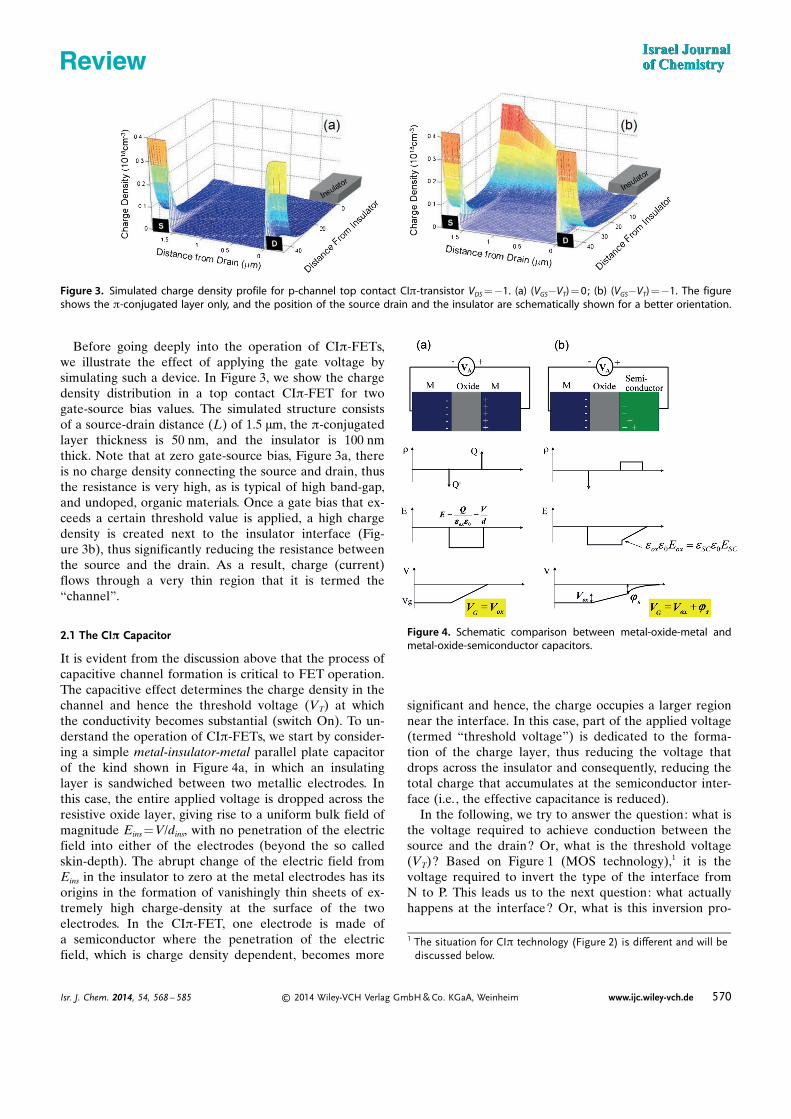
Before going deeply into the operation of CIp-FETs,we illustrate the effect of applying the gate voltage bysimulating such a device. In Figure 3, we show the chargedensity distribution in a top contact CIp-FET for twogate-source bias values. The simulated structure consistsof a source-drain distance (L) of 1.5 mm, the p-conjugatedlayer thickness is 50 nm, and the insulator is 100 nmthick. Note that at zero gate-source bias, Figure 3a, thereis no charge density connecting the source and drain, thusthe resistance is very high, as is typical of high band-gap,and undoped, organic materials. Once a gate bias that ex-ceeds a certain threshold value is applied, a high chargedensity is created next to the insulator interface (Fig-ure 3b), thus significantly reducing the resistance betweenthe source and the drain. As a result, charge (current)flows through a very thin region that it is termed the“channel”.
2.1 The CIp Capacitor
It is evident from the discussion above that the process ofcapacitive channel formation is critical to FET operation.The capacitive effect determines the charge density in thechannel and hence the threshold voltage (VT) at whichthe conductivity becomes substantial (switch On). To un-derstand the operation of CIp-FETs, we start by consider-ing a simple metal-insulator-metal parallel plate capacitorof the kind shown in Figure 4a, in which an insulatinglayer is sandwiched between two metallic electrodes. Inthis case, the entire applied voltage is dropped across theresistive oxide layer, giving rise to a uniform bulk field ofmagnitude Eins =V/dins, with no penetration of the electricfield into either of the electrodes (beyond the so calledskin-depth). The abrupt change of the electric field fromEins in the insulator to zero at the metal electrodes has itsorigins in the formation of vanishingly thin sheets of ex-tremely high charge-density at the surface of the twoelectrodes. In the CIp-FET, one electrode is made ofa semiconductor where the penetration of the electricfield, which is charge density dependent, becomes more
significant and hence, the charge occupies a larger regionnear the interface. In this case, part of the applied voltage(termed “threshold voltage”) is dedicated to the forma-tion of the charge layer, thus reducing the voltage thatdrops across the insulator and consequently, reducing thetotal charge that accumulates at the semiconductor inter-face (i.e., the effective capacitance is reduced).
In the following, we try to answer the question: what isthe voltage required to achieve conduction between thesource and the drain? Or, what is the threshold voltage(VT)? Based on Figure 1 (MOS technology),1 it is thevoltage required to invert the type of the interface fromN to P. This leads us to the next question: what actuallyhappens at the interface? Or, what is this inversion pro-
Figure 3. Simulated charge density profile for p-channel top contact CIp-transistor VDS =�1. (a) (VGS�VT) = 0; (b) (VGS�VT) =�1. The figureshows the p-conjugated layer only, and the position of the source drain and the insulator are schematically shown for a better orientation.
Figure 4. Schematic comparison between metal-oxide-metal andmetal-oxide-semiconductor capacitors.
1 The situation for CIp technology (Figure 2) is different and will bediscussed below.
Isr. J. Chem. 2014, 54, 568 – 585 � 2014 Wiley-VCH Verlag GmbH & Co. KGaA, Weinheim www.ijc.wiley-vch.de 570
Review

cess? To answer this question, in the context of CMOStechnology,i we consider a doped semiconductor beingpart of a capacitor. In Figure 5, the dopants are represent-ed by encircled charge signs, thus the left column de-scribes a P-type and the right column an N-type semicon-ductor, respectively. Before applying a voltage (top ofFigure 5), the semiconductor is electrically neutral whereevery dopant atom is compensated by a free charge.When a negative (positive) bias is applied to N-type (P-
type) based capacitor, positive (negative) charge appearsnear the interface. At first, it is mainly composed ofdopant atoms that have been stripped of their free elec-tron (hole). By depleting the free charges near the inter-face, we create a depletion layer. When the voltage ismade larger, we arrive at a point where, very close to theinterface, free holes (electrons) start to accumulate andcreate a very thin layer whose type has been inverted toP-type (N-type); namely, the type of free charges at theinterface is now opposite to what it was at the “no bias”state.
2.1.1 The Role of the Semiconductor Parameters
How does the process of inversion depend on the materi-al parameters? This is commonly answered with the aidof an energy band diagram (Figure 6), where the positionof the Fermi-level (EF) between the conduction bandedge (EC) and the valence band edge (EV) depicts thedensity of electrons and holes in the semiconductor.For an intrinsic semiconductor, there is an equal density(ni) of electrons and holes and the Fermi-level lies ap-proximately in the middle of the electronic gap. Whenthere is an excess charge, then the Fermi-level shiftsup (down) for excess of electrons (holes) and thecharge density, at the low density limit, is given by
n ¼ nieðEF�EFiÞ
kT ðp ¼ nieðEFi�EF Þ
kT Þ. In the case of a metal, the last(relevant) band is partially filled with electrons (high den-sity) and the Fermi-level lies within the electronic band(see Figure 6).
To invert the type of the material, the Fermi-level atthe interface has to be moved to the other side of EFi
(Figure 6). The voltage shift required for the inversionprocess is: ðVInvert ¼ 2
q � EF � EFi½ �Þ. However, as shown inFigure 5, before inversion is created, a depletion layer isformed. The creation of this space charge is associatedwith a voltage drop ðVDepletion ¼ 1
Cins
ffiffiffiffiffiffiffiffiffiffiffiffiffiffiffiffiffiffiffiffiffiffiffiffiffiffiffiffiffi
2ee0qNDVInvert
pÞ[22] that
adds to the inversion voltage. So the threshold voltageassociated with the semiconductor material is only:VT_Material =VInvert +VDepletion.
Turning now to transistors made using CIp technology(Figure 2):what is the gate voltage required to achieveconduction between the source and the drain? Based onFigure 2, it is the voltage required to populate (charge)the p-conjugated layer. Typically, a well behaved CIp-FET is made using an intrinsic (undoped) p-conjugatedlayer2 and the Fermi level lies approximately in themiddle of the HOMO-LUMO gap (EF�EFi). Therefore,following the above discussion, we note that for an un-doped p-conjugated material, there is no inversion nordepletion and if we follow the convention for Si devicesthen VT Material pjSi¼ 0. However, the true meaning of thethreshold voltage is the value beyond which all the ap-plied bias results in capacitive charging Q= (V�VT)Cins.Since the charge density becomes significant only whenthe Fermi level is brought close to the respective(HOMO/LUMO) level, we get VTMaterialn
ffi 12q Eg. We use
the approximate sign, since in amorphous semiconductorsthe “band edge” is soft and the effective threshold volt-age may be bias dependent (Figure 7).[25]
2.1.2 The Role of the Device Parameters
In the device, we bring together a semiconductor anda metal and let them reach equilibrium through the insu-lating layer3. As we see below, the device structure also
Figure 5. The formation of a depletion layer followed by inversion.
Figure 6. Energy band diagram of intrinsic, N-type, and P-typesemiconductors.
2 The case of doped p layer will be discussed later in the text.3 Even when the insulator is perfect and there is no charge transfer
through it, the situation of common Fermi-level is achieved oncean external source is applied at zero bias (short-circuit).
Isr. J. Chem. 2014, 54, 568 – 585 � 2014 Wiley-VCH Verlag GmbH & Co. KGaA, Weinheim www.ijc.wiley-vch.de 571
Review

makes a contribution to VT. Recall that the Fermi level ofan intrinsic semiconductor lies midway between theHOMO and the LUMO (Figure 6). The Fermi level ofthe semiconductor, as drawn in Figure 8, therefore lies
below that of the metal contact. In making an electricalconnection between the organic layer and the metal, elec-trons will therefore flow from the metal to the semicon-ductor, so as to bring the Fermi-level at the semiconduc-tor up towards the metal Fermi-level; as with the singlelayer devices considered in Ref. [22], this creates a built-in potential of V ¼ 1
q ðFM �FSÞ, which tilts the bands ofthe insulator and the semiconductor upwards. The widthof the spacer layer determines the potential drop across
the semiconductor: in the limit dins =1, the full potentialV ¼ 1
q ðFM �FSÞ is dropped across the insulator, whereasin the limit dins =0, the full potential is dropped across thesemiconductor. To restore the bands of the semiconductor(and insulator) to their flat state, one has to apply a com-pensating external bias of VFB ¼ 1
q ðFM �FSÞ4. Namely, toreach a position where the threshold voltage is dependenton the material parameters, we have to first apply avoltage to compensate for the effect of the structureVT Structure ¼ VFBð Þ. The total threshold voltage isVT ¼ VT Structure þ VT Materialð Þ. Sometimes, during the man-
ufacturing process charges get trapped in the insulator(charged defects), thus affecting the charge balanceacross the insulator and consequently, the degree of bandbending and the magnitude of the flat-band voltage[22] .
In the discussion so far, we considered that the onlybarrier to current flow is the lack of relevant charge carri-ers in the channel region. However, generally speaking,there could also be a barrier at the source metal/p-layerinterface. If such a barrier exists, the device characteris-tics are distorted, including an enhancement of the appar-ent threshold voltage.[24]
3. Possible Applications
It is too early to predict where organic or CIp field effecttransistors will find their main use. It seems to be com-monly accepted that they will not replace inorganic FETsbut rather, be used in products where inorganic transis-tors cannot be used due to their mechanical properties orcost. Such applications could be:
1. Flexible displays, where the CIp-FET is used to ac-tively switch the pixels of light emitting diodes or liquidcrystals.
2. Smart cards or smart tags, which require a relativelylow density of transistors and flexibility in circuit design.High-end products may combine plastic circuitry withplastic displays to provide instant feedback to the user/customer.
3. Pharmaceutical, where the organic nature of thedevice may be used to better couple the device with de-tection capabilities of chemical or biological moieties.
The required performance will naturally depend on theapplication sought, but if logic circuitry is to be used toperform a slightly complex function, then the operatingvoltages will need to be compatible with existing technol-ogies (<5 V) and the current flowing through a singletransistor will need to exceed several mAs to avoid noiseand related errors.
Figure 7. (a) For an intrinsic semiconductor with a sharp bandedge, applying a voltage to the gate will shift the Fermi level to-wards the band. Once the Fermi level approaches the band edge,the Fermi level “locks” and any additional voltage goes for charg-ing the channel (cDV). (b) For a disordered semiconductor wherethe “band edge” is soft, the Fermi level doesn’t lock and goes intothe LUMO density of states.
Figure 8. Band profile of a metal-insulator-semiconductor struc-ture.
4 We assume here that F is given in eV.
Isr. J. Chem. 2014, 54, 568 – 585 � 2014 Wiley-VCH Verlag GmbH & Co. KGaA, Weinheim www.ijc.wiley-vch.de 572
Review
4. The Transistor Characteristics
4.1 The Linear Regime
It is important to understand how the source-drain cur-rent will depend on the source-gate bias. We start by cal-culating the current that will flow across the channel, car-ried by the charge that has been accumulated by the ca-pacitor-effect. Here we assume that the decrease ofcharge density along the channel is small and that thecharge density is to a good approximation uniform alongthe channel (in the z and y directions). If we assume thatthe transistor has the dimensions of W and L (seeFigure 1), we can write the formula for the current IDS
that flows between source and drain as:
IDS ¼#Charge
time¼ QChannel � ðW � LÞ
ttransitð1Þ
where QChannel is the areal charge density in the channeland ttransit is the time it takes a charge to move across thechannel between the source and drain electrodes. If weassume that the electron velocity is characterised bya constant mobility (m), we can calculate the transit timeas:
ttransit ¼Lv¼ L
mE¼ L
m�VDS
L
¼ � L2
mVDSð2Þ
The charge area density (QChannel) can be found fromthe capacitor characteristics, assuming that fs (Figure 4)is bias independent and is fixed at its value for VGS =VT
�sjVG¼VT¼ VInvert
� �
. For the undoped p-layer, this is equiv-alent to the assumption that fs is negligible, since for theintrinsic layer VInvert =0.
Qchannel ¼ �CinsðVGS � VTÞ ð3Þ
Finally, we arrive at the expression for the current:
I ¼ Cins VGS � VTð Þ �W � LL2
mVDS
)
IDS ¼WL
mCins VGS � VTð ÞVDS
ð4Þ
One can also derive the device resistivity in its On
state: RON ¼ VDS
IDS¼ W
L mCins VGS � VTð Þh i�1
and we find it is
a trans-resistor (hence transistor). As Equation (4) repre-sents a linear relation between the current and voltage,the regime for which it holds is called the “linear regime”(Figure 9).
4.2 The Non-Linear Regime and the Saturation Effect
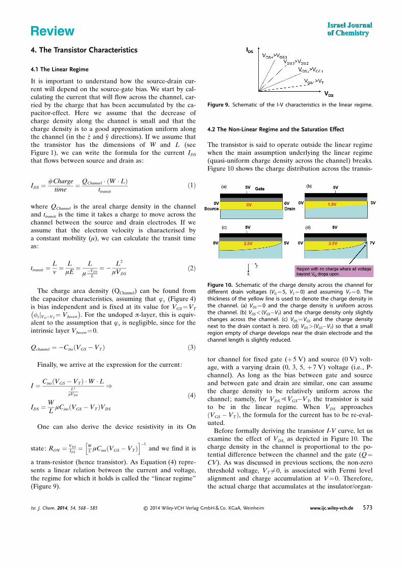
The transistor is said to operate outside the linear regimewhen the main assumption underlying the linear regime(quasi-uniform charge density across the channel) breaks.Figure 10 shows the charge distribution across the transis-
tor channel for fixed gate (+5 V) and source (0 V) volt-age, with a varying drain (0, 3, 5, +7 V) voltage (i.e., P-channel). As long as the bias between gate and sourceand between gate and drain are similar, one can assumethe charge density to be relatively uniform across thechannel; namely, for VDS ! VGS�VT, the transistor is saidto be in the linear regime. When VDS approachesVGS � VTð Þ, the formula for the current has to be re-eval-
uated.Before formally deriving the transistor I-V curve, let us
examine the effect of VDS, as depicted in Figure 10. Thecharge density in the channel is proportional to the po-tential difference between the channel and the gate (Q=CV). As was discussed in previous sections, the non-zerothreshold voltage, VT¼6 0, is associated with Fermi levelalignment and charge accumulation at V=0. Therefore,the actual charge that accumulates at the insulator/organ-
Figure 9. Schematic of the I-V characteristics in the linear regime.
Figure 10. Schematic of the charge density across the channel fordifferent drain voltages (VG = 5, VS = 0) and assuming VT = 0. Thethickness of the yellow line is used to denote the charge density inthe channel. (a) VDS = 0 and the charge density is uniform acrossthe channel. (b) VDS< (VGS�VT) and the charge density only slightlychanges across the channel. (c) VDS = VGS and the charge densitynext to the drain contact is zero. (d) VDS> (VGS�VT) so that a smallregion empty of charge develops near the drain electrode and thechannel length is slightly reduced.
Isr. J. Chem. 2014, 54, 568 – 585 � 2014 Wiley-VCH Verlag GmbH & Co. KGaA, Weinheim www.ijc.wiley-vch.de 573
Review

ic interface is the sum of that found at V=0 and that in-duced by the external voltage: Q=CV�CVT =C(V�VT).The potential across the channel is set bytwo boundary conditions at the source (VS) andat the drain (VD). As VD approaches VG�VT,, thecharge density near the drain is reducedQD ¼ C VD � VG � VTð Þ½ � < C VS � VG � VTð Þ½ � ¼ QSð Þ,
thus enhancing the resistivity of the channel. When thiseffect takes place, the slope of the I-V curve is reduced(higher resistivity) and the curve starts to saturate. OnceVD is equal to VG�VT, a region empty of the channel typecarriers is formed. When the value of VD crosses VG�VT,the size of this “empty” region is enhanced. Since thisregion is “empty” of channel type carriers, its resistivity isvery high and the entire extra potential drops across thisregion5 and the potential at the edge of the channel ispinned at VG�VT. Namely, the region where the channelexists remains with the boundary conditions of VS on oneside and VG�VT on the other for any VD that exceedsVG�VT. As the resistance per unit length is high, thelength of this empty region can be very small and stillprovide the required resistivity to accommodate theexcess potential drop. Since once VD exceeds VG�VT, theboundary conditions of the channel region are fixed andthe current that will flow across the channel will becomeindependent of VD. The resulting curve will be like thatshown in Figure 11.
To derive the I-V curve formally, we recall that thecharge is not uniform across the channel and in realitydecreases rapidly from the start to the end of the channel(see Figure 3). Accordingly, we write Qchannel =Qchannel(y)and its value is:
QchannelðyÞ ¼ �Cins VG � VðyÞð Þ � VT½ � ð5Þ
where V(y) is the electrochemical potential in the channelat point y and ½VG � VðyÞ þ VTð Þ� is the voltage thatdrops across the insulator. Before proceeding, we showthat even in this case, where a charge gradient along thechannel is inherent, the current in a conventional transis-tor is mainly drift current. To do so, we write the expres-sions for the drift and diffusion currents:
mEN ¼ mVðy2Þ � Vðm1Þ
y1 � y2�Nðm1Þ þNðm2Þ
2
D@N@y¼ D
Nðm1Þ þNðm2Þy1 � y2
Inserting Equation (5):
mEN ¼ mVðy1Þ � Vðm2Þ
y1 � y2� Cinsq
�1 VG �Vðm1Þ þ Vðm2Þ
2� VT
� �
D@N@y¼ kT
qmCinsq
�1 Vðm1Þ � Vðm2Þy1 � y2
And finally the ratio between the two currents is:
mEN
D @N@y
�
�
�
�
�
�
�
�
�
�
� VG � VðyÞ � VTkTq
�
�
�
�
�
�
�
�
�
�
ð6Þ
Equation (6) shows that as long as the voltage dropacross the insulator is much larger than kT/q, the currentis mainly drift current and hence we can write:
IDS ¼ IDSðyÞ ¼W mQchannelðyÞEðyÞ ¼W mQchannelðyÞ�dVðyÞ
dy
ð7Þ
Integrating across the channel, we find:
Z
L
0
IDSdy ¼Z
L
0
W mQchannelðyÞ�dVðyÞ
dydy ð8Þ
If VDS � VGS � VTð Þ (Figures 10a to 10c), we can re-place the integration between y=0 and y=L with an in-tegration between V(0)=0 and V(L)=VD.
Z
L
0
W mQchannelðyÞ �dVðyÞdy dy ¼
R
VDS
0
W mCins VGS � Vð Þ � VT½ �dVð9Þ
As the current is constant:
IDSL ¼W mCns VGS � VTð ÞV � V2
2
�
VDS
0
Figure 11. N-type transistor IDS�VDS characteristics for severalvalues of VGS as derived by Equations (10) and (12). Here, W/L =600, Cins = 50 nFcm�2, m= 10�4 cm2 V�1 s�1 and VT = 1 V. The dashedline depicts the transition from linear to saturation regimes.
5 In principle, the region that is empty of channel-type carriers(holes or electrons) may be filled with the other type of carrier(electron or hole). We assume that the conductivity associatedwith this other-type carrier is negligibly small (low mobility, con-tact limited).
Isr. J. Chem. 2014, 54, 568 – 585 � 2014 Wiley-VCH Verlag GmbH & Co. KGaA, Weinheim www.ijc.wiley-vch.de 574
Review

and so finally, for VGS in accumulation regime andVDS � VGS � VTð Þ:
IDS ¼WL
mCns VGS � VTð ÞVDS �V2
DS
2
�
ð10Þ
In the above, we have assumed that: (a) the charges inthe channel are electrons (voltages taken as positive); (b)there is charge in the channel anywhere between y=0and y=L ; and (c) VS and VD can be used as the twoboundary conditions for the channel (see Figure 10). As-sumption (c) is true as long as the contacts are ideal andno (or negligible) voltage drops across them. Assumption(a) is true as long as VDS � VGS � VTð Þ ; however, whenthe magnitude of VDS exceeds that of VGS � VTð Þ,a region empty of charge is created near the drain elec-trode (see Figure 10). In this case, Equation (8) has to berewritten:
Z
LEFF
0
IDSdy ¼Z
LEFF
0
W mQchannelðyÞ�dVðyÞ
dydy where LEFF � L
ð11Þ
Equation (9) turns into
Z
LEFF
0
W mQchannelðyÞ�dVðyÞ
dydy ¼
Z
VGS�VT
0
W mCins VGS � Vð Þ � VT½ �dV
and finally,
IDS SAT ¼W
2LEFFmCins VGS � VT½ �2 ð12Þ
for VGS in accumulation regime and VDS � VGS � VTð Þ.Since the region that is empty of charge has high resis-
tivity it can accommodate relatively high voltage acrossa short distance. In typical transistors, this regionL� LEFFð Þ is small compared to the geometrical channel
length (L) and one can approximate LEFF as LEFF ffi Lð Þ.This approximation breaks for short-channel transistors(as will be briefly discussed later).
Finally, the FET that we have discussed above is exten-sively used in electrical circuits and when it is placed insuch a circuit design-sheet it is drawn using the symbolshown in Figure 12.
5. Extracting Material Parameters of CIp-FET
5.1 Field Effect Mobility
If the current flow through a transistor is only affected bythe transistor channel, then its I-V characteristics shouldfollow Equations (10) and (12); namely:
m ¼
IDS
WLCins VGS�VTð ÞVDS�
V2DS2
� � Linear regime
IDS SATWLCins VG�VT½ �2 Saturation regime
8
>
<
>
:
ð13Þ
Sometimes, it is useful to use the derivative of theabove equations. For example, in the linear regime:
@
@VGSIDS ¼
@
@VGS
WL
mCins VGS � VTð ÞVDS �V2
DS
2
� �
ð14Þ
Applying the derivation:
@
@VGSIDS ¼
@
@VGS
WL
Cins VGS � VTð ÞVDS �V2
DS
2
� �
þmWL
CinsVDS
�
ð15Þ
In cases where the mobility is independent of the gatebias (or charge density), Equation (15) reduces to:
m ¼@
@VGSIDS
WL CinsVDS
� � ð16Þ
and the mobility is proportional to the slope of the curvein Figure 13 in the regime where it is linear. The advant-age of Equation (6) is that it is independent of VT andhence is not prone to errors in the threshold voltage ex-traction; however, the first term in Equation (15) is oftennon-negligible in amorphous organic materials and theuse of Equation (6) will give rise to artificial peaks in themobility versus gate bias curve.
5.2 Background Doping
The above discussion assumes that the p-conjugated layeris undoped and hence, its conductivity is zero unlesscharged (populated) by the applied gate-source bias. Insome cases, there exists a doping density in the p-conju-gated layer, be it intentional or unintentional.[26–28] Inmost cases, the doping would be of the same type as the
Figure 12. The electrical symbol describing N- and P-channel FETs.
Isr. J. Chem. 2014, 54, 568 – 585 � 2014 Wiley-VCH Verlag GmbH & Co. KGaA, Weinheim www.ijc.wiley-vch.de 575
Review
channel, although recently, inversion type FETs have alsobeen reported.[28] In the most common case, there wouldbe two effects due to doping: (a) the Fermi level wouldshift (typically maximum 1 V) and the flat band voltage(VFB) would shift accordingly; (b) at high enoughdoping, a finite conductivity between the source anddrain electrodes appears and is associated with the bulkconductivity of the p-conjugated layer. The bulk conduc-tivity is electrically in parallel with the channel conductiv-ity.
IDS Bulk ¼ qNDWL
mdpVDS ð17Þ
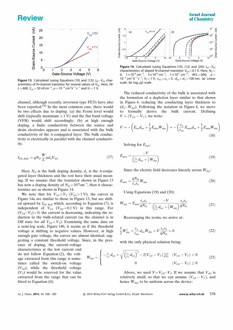
Here ND is the bulk doping density, dp is the p-conju-gated layer thickness and the rest have their usual mean-ing. If we assume that the transistor shown in Figure 13has now a doping density of ND =1016cm�3, then it charac-teristics are as shown in Figure 14.
We note that for VGS>VT (VGS>1 V), the curves inFigure 14a are similar to those in Figure 13, but are shift-ed upward by IDS Bulk which, according to Equation (7), isindependent of VGS (VDS =0.1 V) in this range. For(VGS�VT)<0, the current is decreasing, indicating the re-duction in the bulk-related current (as the channel is inOff state for all VGS<VT). Examining the same data ona semi-log scale, Figure 14b, it seems as if the thresholdvoltage is shifting to negative values. However, at highenough gate voltage, the curves are almost identical, sug-gesting a constant threshold voltage. Since, in the pres-ence of doping, the current-voltagecharacteristics at the low current enddo not follow Equation (2), the volt-age extracted from this range is some-times called the switch-on voltage(VSO), while the threshold voltage(VT) would be reserved for the valueextracted from the range that can befitted to Equation (0).
The reduced conductivity of the bulk is associated withthe formation of a depletion layer similar to that shownin Figure 4, reducing the conducting layer thickness to(dp�Wdep). Following the notation in Figure 4, we moveto formally derive the bulk current. DefiningV ¼ VGS � VTð Þ, we write:
V ¼ � Einsdins þ12
EmaxWdep
�
¼ � ep
einsEmaxdns þ
12
EmaxWdep
�
ð18Þ
Solving for Emax :
Emax ¼�V
ep
einsdins þ 1
2 Wdep
� � ð19Þ
Since the electric field decreases linearly across Wdep :
Emax ¼qND
epe0Wdep ð20Þ
Using Equations (19) and (20):
Wdep ¼ Emaxepe0
qND¼ �V
ep
einsdins þ 1
2 Wdep
� �
epe0
qNDð21Þ
Rearranging the terms, we arrive at:
12
W2dep þ
ep
einsdinsWdep þ V
epe0
qND¼ 0 ð22Þ
with the only physical solution being:
Wdep ¼� ep
einsdins þ
ffiffiffiffiffiffiffiffiffiffiffiffiffiffiffiffiffiffiffi
ep
einsdins
� �2r
� 2 VGS � VTð Þ epe0
qNDVGS � VTð Þ < 0
0 VGS � VTð Þ � 0
8
>
<
>
:
ð23Þ
Above, we used V=VGS�VT. If we assume that VDS isrelatively small, so that we can assume VGS � VTð Þ, andhence Wdep, to be uniform across the device:
Figure 13. Calculated (using Equations (10) and (12)) IDS�VGS char-acteristics of N-channel transistor for several values of VDS. Here, W/L = 600, Cins = 50 nFcm�2, m= 10�4 cm2 V�1 s�1 and VT = 1 V.
Figure 14. Calculated (using Equations (10), (12) and (24)) IDS�VGS
characteristics of doped N-channel transistor VDS = 0.1 V. Here, ND =0, 1 � 1016 cm�3, 3 � 1016 cm�3, 1 � 1017 cm�3; W/L = 600; m=10�4 cm2 V�1 s�1; VT = 1 V; eins =ep = 3; dins = dp = 100 nm. (a) Linearscale. (b) log10(y) scale.
Isr. J. Chem. 2014, 54, 568 – 585 � 2014 Wiley-VCH Verlag GmbH & Co. KGaA, Weinheim www.ijc.wiley-vch.de 576
Review

IDS Bulk ¼ qNDWL
m dp �Wdep
� �
VDS ð24Þ
We observe that the current drops to zero once the de-pletion layer extends across the entire p-conjugated layer.If we know the voltage at which it happens, we can useEquations (18) and (20) to derive the dopant density(Wdep =dp):
ND ¼�2Vpinche0
q d2p
epþ 2dpdins
eins
� �
For example, based on Figure 14, we find for the high-est doping Vpinch ¼ VGS
IDS¼0�VT ¼ �9V and hence
ND ¼2 � 9 � 8:85 � 10�14
1:6 � 10�19 ð100�10�7Þ3 þ 2�100�10�7 �100�10�7
3
� � ¼ 9:94 � 1016½cm�3�
A more comprehensive treatment of doped devicesthat includes the effect of non-uniform Wdep can be foundin Ref. [26].
To conclude this section, we plot the same calculationas in Figure 14, but let the mobility be charge density de-pendent ðm / N0:5Þ so as to mimic some of the disorderedmaterial based FETs.[29–30] We note that in this case, thereis a kink in the curves that is reminiscent of the thresholdvoltage (Figure 15).
6. Advanced Topics
6.1 The Channel Depth
In the development of the I-V characteristics above, wedid not consider the charge density profile along the x-axis (Figure 16). This was justified by the assumption wemade for Equation (3) that fs (see Figure 4) is constantonce the gate voltage is above threshold. In other words,we neglected any changes in the charge profile and theassociated change in the voltage drop across it. Addingthis effect rigorously will significantly complicate the
expressions, as for each point along the y-axisthere exists a different effective capacitance andCIns ) CIns EFF ¼ CIns EFF VGS; yð Þ.
In the present text, we try instead to examine the valid-ity of our assumption and give the reader a sense for theassociated effect on the device performance. To derive anexpression for the charge profile perpendicular to the in-sulator, we start with the basic current continuity andPoisson equations:
Jh ¼ qpmh � E� q@
@xDhpð Þ ¼ qpmh � E� qDh
@
@xp� qp
@
@xDh
ð25Þ
At steady-state, there is no current flow in the x direc-tion and if we assume Dh
@
@x p p @
@x Dh, we arrive at:
Jh ¼ qpmh � E� qDh@p@x¼ 0 ð26Þ
and the boundary conditions for the electric field are:
Ejx¼0¼ep
einsEins �
ep
eins� VG � VTð Þ � VðyÞ
dins; Ejx¼dp
¼ 0 ð27Þ
Using (26) and the Poisson equation, we can derive:
E@E@x¼ Dh
mh
@2E@x2
ð28Þ
or
12@
@xE2 ¼ Dh
mh
@
@x@E@x
ð29Þ
Integrating over x once (assuming D/m to be a slowlyvarying function of x):
Figure 15. Calculated (using Equations (10), (12) and (24)) IDS�VGS
characteristics of doped N-channel transistor VDS = 0.1 V. Here, ND =0, 1 � 1016 cm�3, 3 � 1016 cm�3, 1 � 1017 cm�3; W/L = 600; m/N0.5 ;VT = 1 V; eins =ep = 3; dins = dp = 100 nm. (a) Linear scale. (b) log10(y)scale.
Figure 16. Simulated charge density (2D simulation) and potentialat the middle of the channel for p-channel transistor and a bias ofVDS = (VGS�VT) =�1. XChannel denotes the effective channel depth (~7 nm here).
Isr. J. Chem. 2014, 54, 568 – 585 � 2014 Wiley-VCH Verlag GmbH & Co. KGaA, Weinheim www.ijc.wiley-vch.de 577
Review

mh
2DhE2 þ C ¼ @E
@xð30Þ
where C is a constant to be determined by the boundaryconditions. Integrating between point x to the air inter-face (dp) we arrive at:
Z
dp
x
@x0 ¼Z
0
E
@E0mh
2DhE02 þ C
ð31Þ
and if D/m is approximately constant across the layer:
E ¼ffiffiffiffiffiffiffiffiffiffiffiffi
2CDh
mh
r
tan
ffiffiffiffiffiffiffiffiffi
Cmh
2Dh
r
ðx� LÞ" #
ð32Þ
This electric field creates “band” bending across the p-conjugated layer that is directly derived from the exis-tence of charge at the channel. The bending across theentire layer is:
DVchannel ¼ �Z
L
0
Edx ¼ �ffiffiffiffiffiffiffiffiffiffiffiffi
2CDh
mh
r
Z
L
0
tan
ffiffiffiffiffiffiffiffiffi
Cmh
2Dh
r
ðx� LÞ" #
dx ¼ � 2Dh
mhlog cos
ffiffiffiffiffiffiffiffiffi
Cmh
2Dh
r
L
" # !
ð33Þ
and the charge density across the p-conjugated layer is:
p ¼ epe0
q@E@x¼ Cepe0
qtan
ffiffiffiffiffiffiffiffiffi
Cmh
2Dh
r
ðx� LÞ" #2
þ1
!
ð34Þ
where C is to be determined from:
eins
ep
Eins ¼ Ejx¼0¼ffiffiffiffiffiffiffiffiffiffiffiffi
2CDh
mh
r
tan
ffiffiffiffiffiffiffiffiffi
Cmh
2Dh
r
ð0� LÞ" #
ð35Þ
To illustrate the use of Equations (32) to (35), we cal-culated the charge density profile for two different elec-tric fields at the insulator (E0). The first one was chosento be close to the conditions used for Figure 16 and thesecond for a higher applied voltage. We first use Equa-tion (35) to find the integration constant C (Table 1) and
then use Equation (34) to calculate the charge densityprofile (T=300 K).
Examining Figure 17, we note that at low voltage dropacross the insulator, the channel is rather extended andthe charge density extends a considerable way into the p-conjugated layer. The functional form of the density dis-
tribution tells us that for a thinner p-conjugated layer, theeffect will be more pronounced. Also, at higher appliedbias, the channel becomes more confined as most of theadded charge accumulates near the insulator interface. Fi-nally, the inset shows the effect of the enhanced Einstein-relation as discussed in Refs. [21,32–33], and demon-strates that for higher values of D/m, the charge is morespread across the polymer. As the low field result sug-gests, for a relatively thin layer, the channel depth wouldbe dictated by the film thickness and the charge densitywould change significantly less between the insulator andair interface. Under such conditions, one can utiliseKelvin probe techniques to probe the channel propertiesand extract the generalised Einstein relation or the densi-ty of states.[34–35]
To complete the picture, we mention that it has beenshown that organic amorphous (disordered) semiconduc-tors are degenerate at all practical densities[31] and hence:Dm ¼ h
kTq with h being a function of the charge densi-
ty[31–32] . For example, using the calculation shown in theinset to Figure 17 (h=2), DVChannel ffi 0:25 eV. Also,a change in the value of the band bending (DVChannel) isan indication that the chemical potential (quasi Fermilevel, EF) in the p-conjugated layer is also shifting, thusmodifying the effective threshold voltage (this is on topof the effect of the soft “band edge” discussed previous-ly)[25] .
Table 1. The parameters used for Figure 17.
Eins [Vcm�1] dp [cm] C DVchannel [V]
5 ·104 50·10�7 3.5457e +009 0.0693 ·105 50·10�7 4.7943e +009 0.153
Figure 17. Calculated charge density profile for two electric fieldsat the insulator (different VGS). The right axis is for E0 = 5 �104 V cm�1 and the left axis for E0 = 3 � 105 V cm�1 (ep = 3). The insetshows the effect of D/m being a (slowly-varying) function of thecharge density (E0 = 5 � 104 V cm�1). The full line in the inset wascalculated using D/m= 2 kT/q (see Ref. [31]) and only the first10 nm are shown.
Isr. J. Chem. 2014, 54, 568 – 585 � 2014 Wiley-VCH Verlag GmbH & Co. KGaA, Weinheim www.ijc.wiley-vch.de 578
Review

Next we move to also evaluate a simple expression forthe effective channel depth. If we define XChannel as thedepth at which the charge density drops to its e�1 value:
e1 ¼ px1
px2
¼ exp � mx1
Dx1
Df12
�
! Df12 ¼ �Dx1
mx1
ð36Þ
If the decay was exponential with x, then XChannel wouldaccommodate ~60% of the charge, but in practice it isusually less; namely, the average electric field would be~80% of its maximum value (or more) and hence:
0:8eins
ep
EinsXChannel ¼Em
ð37Þ
and
XChannel �dins
VG � VðyÞep
eins
kTq
h ð38Þ
Using common parameters as dins =100e�7cm,VGS�VT =1V; VDS =1V we find that near the sourceVG � VðyÞ ¼ VGSð Þ XChannel =2.6 nm � h and at the centre
of the channel VG � VðyÞ � VT ffi 0:5Vð Þ XChannel =5.2 nm� h. Note that the approximate expression of Equa-tion (37) is in good agreement with the numerical simula-tion results shown in Figure 16. Namely, in organic tran-sistors where the molecular distance is about 0.5 nm, thechannel will extend over several monolayers, especially atlow gate bias. We reiterate that a more precise expressionfor XChannel can be derived directly from Equation (34).
6.2 Switch On (Transient Dynamics)
FETs are largely used as a switching element in a circuit,the speed of which is determined by the time it takes toswitch the transistor On (and Off). Therefore, it is essen-tial that we have some understanding of the mechanismby which the transistor channel is built as a function oftime[36–38] . We also take this opportunity to look moreinto the operation of the top contact CIp-FET structure(see Figure 2). Figure 18 shows the charge density and po-tential distribution at about 100 ns after the gate voltagehas been switched from VG =0 to VG =�5 V, while keep-ing the source and drain voltage constant at VS =0 andVD =�3 V, respectively.
At first, the source and drain are isolated from eachother (as the channel that will connect them has not beenformed yet). At this short time, we mainly see the capaci-tive nature of the FET structure that was discussed in sec-tion 2.1. Namely, the region under the drain and sourcecontacts is charged and the voltage applied to the sourceand drain is projected onto the insulator interface. Thissituation is illustrated in Figure 19.
After the source and drain have been projected ontothe insulator interface, the channel will start to form
through the charged regions underneath the contacts. Ana�ve estimate of the time it would take to build thechannel would be to consider the time it would take fora charge to drift the channel length under the appliedsource drain bias:
Dt ¼ LmE¼ L2
mVDS¼ ð5 � 10�4Þ2
5 � 10�3 � 3 ¼ 16:66ms ð39Þ
However, examining Figure 18b, we note that at this in-itial stage, the voltage actually drops across a much short-er distance and only across the part of the channel thathas been filled (also see Equation (5)). In Figure 20, weplot the simulated charge build up at the channel, whichis similar6 in shape to the potential across it (P�CinsV).We note that the channel is built within less than 5 ms,being less than a third of the na�ve value of 16.66 ms cal-culated above. The relation between the charge density(P) and the potential (V) has also been used in a time-de-pendent Kelvin-probe measurement to experimentallymonitor the channel build-up[37] .
As P�CinsV, we also note that the drain-source biasdrops across the entire channel length only after theentire channel has been formed. The equivalent circuitdescribing the channel build up is as shown in Figure 21.
Figure 18. Charge density (a) and potential (b) distribution fora top contact CIp-FET shortly after switching the gate voltage from0 to �5 V (VDS =�3 V).
Figure 19. Equivalent circuit description of the FET immediatelyafter switching the gate voltage.
6 The deviation is related to the potential drop across the channelitself as described in Equation (33).
Isr. J. Chem. 2014, 54, 568 – 585 � 2014 Wiley-VCH Verlag GmbH & Co. KGaA, Weinheim www.ijc.wiley-vch.de 579
Review

In Figure 21, RS and RD are the contact resistances,which would be negligible in a well-behaved FET. Ri,i+ 1 isthe serial resistance associated with the current that flowsthrough, and fills up, the channel. The charge density ateach node is calculated using the voltage dropping acrossthe gate insulator at the position of the node (rememberthat a minimum voltage drop of VT is required to bringthe Fermi level close enough to the transport band andinitiate charging):
pi ¼Cins Vi�VGð Þ�VT½ �
q Vi � VGð Þ � VT½ � > 0
nidp else
(
½cm�2� ð40Þ
Here, ni times dp represents the 2D residual chargedensity in the film that is not due to any bias (since we as-sumed an intrinsic semiconductor, we use ni here). Equa-tion (40) is written assuming a P-channel and a similar ex-pression can be written for the N-channel where the ap-plied bias has the opposite sign. The resistance, Ri,i+ 1, isderived from the conductivity using the average chargedensity of the nodes at its two ends:
Ri;iþ1 ¼DLW
1qm
p1þpiþ1
2
½W� ð41Þ
where DL is the distance separating two elements (typi-cally, dividing the channel into 10 elements is enough tocapture the distributed nature of the charge build up).
To solve the circuit in Figure 21, we must define theboundary conditions:
V1 ¼ VS; Vnþ1 ¼ VD;
for i6¼1; nþ 1 Vi t¼0 ¼ 0j
(
To calculate the dynamics of the system, we rely on thecapacitor characteristics, which state that the current en-
tering (charging) the capacitor is Ii ¼ c dVi
dt
� �
and onKirchhoff�s law, which states Ii ¼ IRi�1
� IRi, to give:
dVi
dt¼ 1
Cins �W � DLVi�1 � Vi
Ri�1� Vi � Viþ1
Ri
�
ð42Þ
If m is field and density independent and Vi are all posi-tive, we arrive at an expression similar to the continuousform[37]:
dVi
dt¼ m
2DL2 V2i�1 � 2V2
i þ V2iþ1
� � ð43Þ
and finally, the transient currents take the form of:
ISðtÞ ¼ VS�V2ðtÞR1
IDðtÞ ¼ VD�VnðtÞRn
8
<
:
ð44Þ
To illustrate the use of Equations (41) to (44), we havecalculated the transient current measured at the sourceusing parameters similar to those used in the 2D numeri-cal simulation that resulted in Figure 20. The solid line iscalculated for VGS =VDS =�5 V and the dashed line forVDS =�3 V. We note that the two curves are identical butfor the last microseconds. This is expected, since at earlytimes the drain voltage has no effect on the charge densi-ty near the source contact (see Figure 20). ExaminingFigure 20, we note that the charge distribution near thedrain affects the source only at about t=3 ms, which is invery good agreement with the point at which the twocurves in Figure 22 start to deviate. Namely, Equa-tions (41) to (44) are a reasonably good approximationfor the physical picture studied here and experimentallymeasured in Ref. [38]. As Equation (44) suggests, thecompletion of channel charging could also be detected ifone measures the source and drain currents separatelyand looks for the point in time where the two becomeequal.[39]
The above equations suggest that the transistor switchOn characteristics are rather universal and only dependon the channel length and the insulator capacitance.However, there is a hidden dependence which may make
Figure 20. Charge density distribution at the channel as a functionof time (m= 5 � 10�3 cm2 V�1 s�1) after switch On.
Figure 21. The equivalent distributed circuit describing the chan-nel build up.
Isr. J. Chem. 2014, 54, 568 – 585 � 2014 Wiley-VCH Verlag GmbH & Co. KGaA, Weinheim www.ijc.wiley-vch.de 580
Review

the transient curve material dependent. Since the mobili-ty may be charge density dependent,[30,40–42] and this de-pendence varies with the morphology of the p-conjugatedlayer, the functional form of this transient curve is nolonger necessarily universal in shape.
7. Other Structures
7.1 The Vertical Field Effect Transistor
Field effect transistors based on amorphous semiconduc-tors and especially on poorly crystalline organic materialsare attractive due to their low cost and their potential forlarge area electronic device manufacturing via printingmethodologies. An inherent disadvantage of several or-ganic semiconductors is their low carrier mobility whencompared to crystalline materials, which in turn may re-quire different device architectures to achieve certain per-formance goals. In this context, several types of verticalfield-effect transistors (VFETs)[43–46] have been gaining in-terest in the field of organic electronics[23,47–48] . For thecurrent discussion, two relevant structures were inventedin 2003[49] and 2006.[50] The essence of the device structureis described in the paper by Ma et al.[23] and is shown inFigure 23. This architecture consists of all the layersstacked on top of each other in a sequence that is differ-ent to the static induction transistor case.[43,47]
Placing a metal layer between the gate/gate oxide andthe semiconductor makes it close to impossible to induce
any effect in the semiconductor, due to the shielding ofthe gate field by the source electrode. In the architectureof Ma and coworkers, this problem was circumvented byusing an ultrathin metal layer for the source in combina-tion with a super-capacitor, enabling very high fields atthe metal interface. Another method to overcome thesource shielding was developed by creating a perforated(patterned) electrode[48,51] such that the gate-field couldpenetrate through the holes in the conductor layer andthus alleviate the need for a super-capacitor. An evensimpler design of the electrode was realised more recentlyby the use of a carbon nanotube mesh.[20,52–54] While theuse of nanotubes offers a much simpler process, the useof a perforated metal layer offers better control over theelectrode’s properties[15] and render it suitable for the de-tailed modelling[55–56] that could be used to enhance itsperformance[57–58] and open the way to designs based onsemi-standard lithography.[59]
While publications on OFETs are numerous, verticalorganic FET (VOFET) research is quite new and thenumber of publications following the 2004 paper is shownin Figure 24. We can conclude that the volume of re-
search done worldwide so far is very limited compared tothe VOFET�s practical potential – although it is clearlyon the rise. We expect very soon that a number of re-search efforts will come to maturation, which will furtherextend the versatility of this platform.
7.1.1 Mechanisms of Operation – The Schottky Based Transistor
Figure 25 shows a 3D illustration of both lateral (a) andvertical (b) Metal-Oxide-Semiconductor (MOS)-OFETs.Both designs share the same functional layers: gate, gatedielectric, source, semiconductor, and drain. While in lat-eral devices the channel length L – perhaps the most im-portant structural parameter – is determined by lithogra-phy processes, in the vertical design, it is simply deter-mined by the semiconductor layer thickness. Hence, L
Figure 22. Calculated (Equation (44)) transient current for a gatevoltage step between 0 and �5 V. The solid line is calculated forVDS =�5 V and the dashed line for VDS =�3 V.
Figure 23. (a) The vertical structure invented by Yang and Ma[49]
that consisted of a layer sequence of gate electrode, gate insulator,ultra-thin source electrode, semiconductor, drain electrode. (b) Themodified vertical structure,[48, 50] where the ultra-thin source elec-trode was replaced by a perforated one.
Figure 24. VOFET publications since 2004. The list includes publi-cations from the following years: 2004,[23] 2007,[60–61] 2008,[52,62]
2009,[15] 2010,[54,63–64] 2011,[20,55–56,65–67] 2012,[53,57–58,68–69] and2013.[39,59,70–73]
Isr. J. Chem. 2014, 54, 568 – 585 � 2014 Wiley-VCH Verlag GmbH & Co. KGaA, Weinheim www.ijc.wiley-vch.de 581
Review

can be easily downscaled to a few tens of nanometres,counterbalancing the low mobility of organic semiconduc-tors and doing away with complex lithography process-es.[52,57]
As mentioned in the previous section, for the gate fieldto affect the transistor, the natural shielding of the sourceelectrode should be overcome. In the structure proposedby Ma and Yang,[23,49] the electrode is made very thin, andon top of that, the insulator contains mobile ions suchthat the gate capacitor acts as a super capacitor with allthe gate bias falling on the electrode interface. In thestructure proposed by Ben-Sasson et al. ,[15,48,50] the elec-trode is non-continuous or perforated. In the following,we use Figure 26 to explain the basics of the patternedsource VFET. Figure 26a shows again the schematic ofthe transistor structure in which the patterned electrodeis presented as having circular holes. In Figure 26b, wezoom on one of the holes (perforations) and show theregion into which charges will flow, thus defining a basicunit of the vertical FET. In Figure 26c and Figure 26d, weshow a cross section of a single hole and the source metalsurrounding it. Figure 26c shows that if we don�t use thegate bias to turn on the device (VG < VT), then the deviceacts like a metal-semiconductor-metal Schottky diode andthe Off current is kept low by making sure that the barri-er for injection is high. This sub-figure also defines twoimportant structural parameters: the perforation width/di-ameter (D) and the thickness of the source electrode (hs).To understand the VFET operation in the On state, weturn to Figure 26d. Let us first ignore the upper part andthe existence of a drain electrode. We observe a gate die-lectric, where there is the gate electrode on one side andon the other side, it looks as if there are two electrodes.Namely, the structure looks like a bottom contact lateralfield effect transistor (see Figure 2). Due to the high in-jection barrier, this is a Schottky type thin film transis-tor[22] where, by applying a gate field, a channel can becreated.
Once a “channel” is formed in the perforation (hole),charges accumulate close to the insulator interface. Thischarge density can be high enough to so that the Fermilevel in the channel is close to the relevant transportband. In this case, we can consider the channel of the
“lateral transistor” as a virtual contact for the verticaltransistor.[55–56] However, it is not clear how charges thatare pulled towards the insulator by the gate field can beconsidered as an injection contact for the channel thatneeds to form in the vertical direction. This is resolved ifwe recall Figure 16 and Figure 17, which show that due tothe presence of diffusion, there is a tail that extends awayfrom the insulator interface. By applying a drain voltage,a field is created between the source and drain and itpulls the charges, which diffused away from the insulator,to create a drift current in the vertically formed chan-nel.[55–56] This is depicted in Figure 27, which shows a 2D
Figure 25. Illustration of MOS-OFETs, the labels S, G, and D indi-cate the source, gate, and drain electrodes, respectively. Blue andgreen regions indicate the insulating layer and the semiconductorlayer, respectively. Electrodes are indicated by yellow and gray col-ours. (a) Lateral transistor with bottom gate and bottom contacts(BGBC) configuration. (b) Patterned source VOFET architecture. (c)VOFET cross section
Figure 26. Illustration of the Patterned Electrode-SemiconductorSchottky Barrier-based VOFET operational mechanisms. (a) VOFETstructure functional elements are spatially defined by the perfora-tion regions in the Patterned Electrode (PE). (b) Formation of thevirtual contact on top of the insulating layer inside the perfora-tions. The current regimes are shown on the cross section ofa single perforation. (c) Off current which flows from the top of thesource electrode due to drain-source bias. (d) On current flowsfrom the virtual contact, that was formed by the gate, to the drainelectrode.
Figure 27. Charge concentration distribution, logarithmic scaled,for a device with structural parameters of D = 60 nm, hd = 50 nm,hs = 6 nm, fb0 = 0.6 eV and L = 100 nm, and biasing conditions: VG =5 V, VS = 0 V, VD = 2 V.
Isr. J. Chem. 2014, 54, 568 – 585 � 2014 Wiley-VCH Verlag GmbH & Co. KGaA, Weinheim www.ijc.wiley-vch.de 582
Review
numerical simulation result of the charge density distribu-tion for a VFET in the On state.
As Figure 27 shows, the charge density decays exponen-tially away from the gate insulator up to a point where itbecomes constant. The exponential decay indicates theregion where diffusion dominates (see also Figure 16 andFigure 17). The almost constant density region (the verti-cal channel) is governed by drift current. This indicatesthat the closer to the insulator the drain field can startpulling charges, the higher the current would be or thebetter the virtual contact would be. For this to be effec-tive, we need the electric field induced by the drain toreach the bottom of the perforation. This is hampered bythe presence of the source electrode surrounding the vir-tual contact since the field lines would tend to terminateat the source metal electrode. This is where the aspectratio of the hole ðD
hSÞ becomes important.[57] If this aspect
ratio is not large enough, then the field is not able toreach inside and pull at a high enough charge density.This effect is shown in Figure 28a through a simulation ofdevices with varying source electrode thickness and inFigure 28b where two otherwise identical VOFETs werefabricated using source metal layers of 7 nm and 13 nm.
Using Figure 26d, we described the creation of the vir-tual electrode as a creation of a channel in a bottom con-tact lateral FET. Kleemann et al. have shown that by re-placing the bottom contact configuration with a top con-tact one (i.e. , inserting a semiconductor layer betweenthe source and insulator layers),[59] excellent device per-formance can be achieved.
7.1.2 VOFET Analytical Description – a FET or a Diode?
Since the device operation is governed by many structuraland physical details, an analytical description can only beapplied to a simplified model. Under this model, thedevice behaves similar to a diode and the gate�s role is tochange the characteristics of one of the diode electrodes;in our case, the source electrode. We were able to
show[55–56] that when the gate is unbiased, the current re-gimes take the form of a Schottky diode being limited byinjection from the source to the semiconductor (Equa-tion (45)). On the other hand, when the gate is fullybiased, we assume that the patterned source electrodeperforations are saturated with charge carriers, and hencethese regions act similar to an ohmic contact. As a result,in this situation the current regime would be similar tothat found in a space charge limited (SCL) diode (Equa-tion (46)). The full details of Equations (45) and (46) canbe found in Refs. [55–57]; note that the fill factor (FF)parameter, a parameter we added here to both equations,which is the patterned electrode fill factor (the ratio be-tween the electrode metallic area and perforations area),is a very simplified model, shown to underestimate theimportance of the perforations� aspect ratio.
JOff ¼ qmnN0 exp � qkT
�b0 �ffiffiffiffiffiffiffiffiffiffiffiffiffiffiffiffiffiffiffiffi
q � VDS
4pe0eLOff
s
! !
VDS
LOff� ð1� FFÞ
ð45Þ
JOn ¼98
e0emnV2
DS
L3 � FF ð46Þ
This simplified analytical description yields a numberof insights:
On/Off current ratio is a strong function of the Schott-ky barrier height, unlike in lateral OFETs where contactsare ideally ohmic;
On/Off ratio increases as channel length decreases, anopposite trend to the one found in short channel lengthOFETs;
Given a specific channel length, the applied drain biasis determined for the maximization of On/Off per-formance.
Based on data fitting to Equations (45) and (46), twoimportant parameters can be extracted. The first is thepotential barrier between the source and the semiconduc-tor, denoted in Equation (45) as fb0. The second is thebulk materials charge carrier mobility, denoted in Equa-tion (46) as m.
7.1.3 Vertical FETs as Efficient Switching Elements
As a result of the vertical OFET�s short channel length, itcan drive high current densities, operate at low-powerconsumption, and at high-frequency, as shown inFigure 29 ((a) and (d)), making it an ideal candidate, forexample, to drive active matrix OLED pixels. A set of re-sults produced in this work indicate that this device isalso a potentially ideal candidate for low mobility semi-conductor-based logic circuits. Firstly, the device transfercharacteristics (IDS�VGS) shown in Figure 29a demon-strate an On/Off current ratio exceeding 104. Our study
Figure 28. (a) Simulated transfer characteristics of devices withvarying source electrode thickness (hs) values.[55] Inset: On/Off ratiovs. source electrode thickness. (b) Measured transfer characteristicsof N-type VOFETs having source electrode thicknesses of 7 nm(square symbols) and 13 nm (round symbols).[57]
Isr. J. Chem. 2014, 54, 568 – 585 � 2014 Wiley-VCH Verlag GmbH & Co. KGaA, Weinheim www.ijc.wiley-vch.de 583
Review
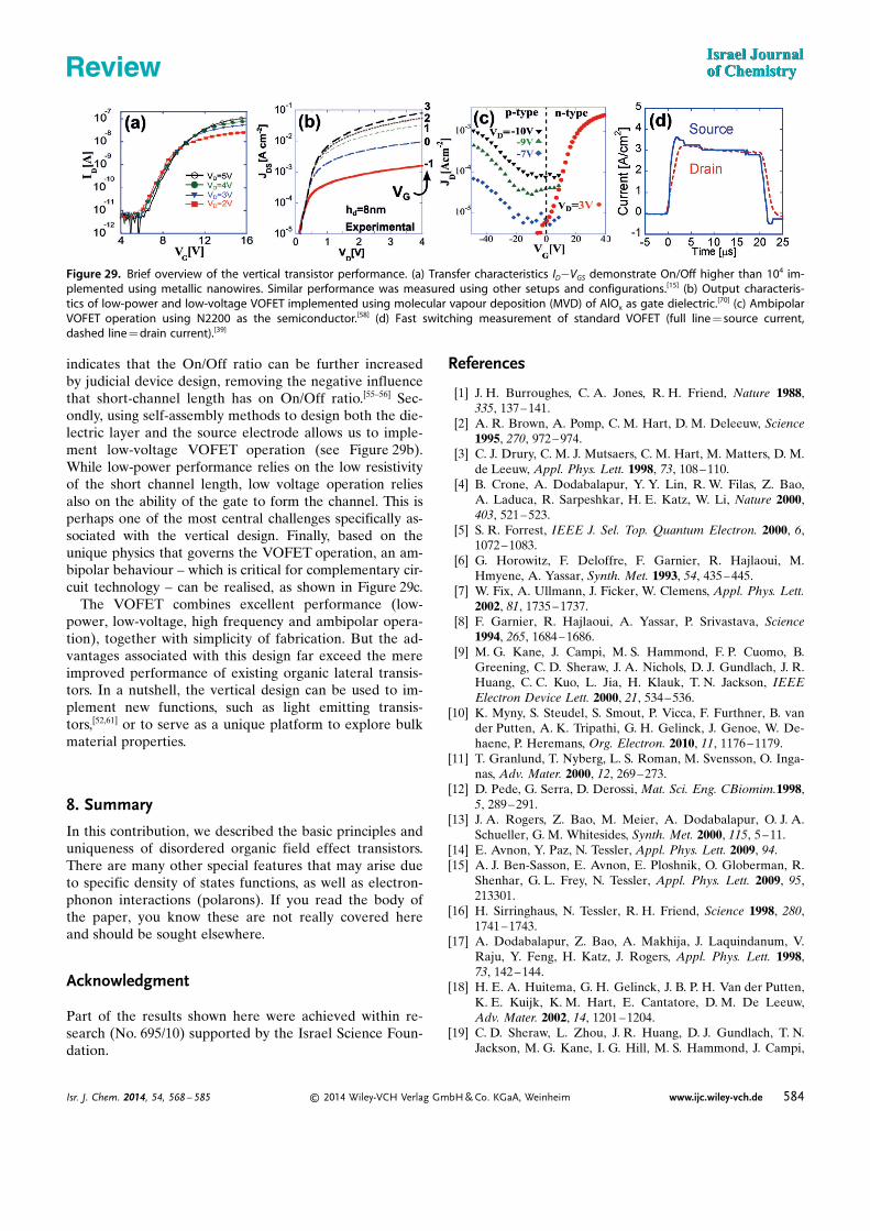
indicates that the On/Off ratio can be further increasedby judicial device design, removing the negative influencethat short-channel length has on On/Off ratio.[55–56] Sec-ondly, using self-assembly methods to design both the die-lectric layer and the source electrode allows us to imple-ment low-voltage VOFET operation (see Figure 29b).While low-power performance relies on the low resistivityof the short channel length, low voltage operation reliesalso on the ability of the gate to form the channel. This isperhaps one of the most central challenges specifically as-sociated with the vertical design. Finally, based on theunique physics that governs the VOFET operation, an am-bipolar behaviour – which is critical for complementary cir-cuit technology – can be realised, as shown in Figure 29c.
The VOFET combines excellent performance (low-power, low-voltage, high frequency and ambipolar opera-tion), together with simplicity of fabrication. But the ad-vantages associated with this design far exceed the mereimproved performance of existing organic lateral transis-tors. In a nutshell, the vertical design can be used to im-plement new functions, such as light emitting transis-tors,[52,61] or to serve as a unique platform to explore bulkmaterial properties.
8. Summary
In this contribution, we described the basic principles anduniqueness of disordered organic field effect transistors.There are many other special features that may arise dueto specific density of states functions, as well as electron-phonon interactions (polarons). If you read the body ofthe paper, you know these are not really covered hereand should be sought elsewhere.
Acknowledgment
Part of the results shown here were achieved within re-search (No. 695/10) supported by the Israel Science Foun-dation.
References
[1] J. H. Burroughes, C. A. Jones, R. H. Friend, Nature 1988,335, 137–141.
[2] A. R. Brown, A. Pomp, C. M. Hart, D. M. Deleeuw, Science1995, 270, 972–974.
[3] C. J. Drury, C. M. J. Mutsaers, C. M. Hart, M. Matters, D. M.de Leeuw, Appl. Phys. Lett. 1998, 73, 108–110.
[4] B. Crone, A. Dodabalapur, Y. Y. Lin, R. W. Filas, Z. Bao,A. Laduca, R. Sarpeshkar, H. E. Katz, W. Li, Nature 2000,403, 521–523.
[5] S. R. Forrest, IEEE J. Sel. Top. Quantum Electron. 2000, 6,1072–1083.
[6] G. Horowitz, F. Deloffre, F. Garnier, R. Hajlaoui, M.Hmyene, A. Yassar, Synth. Met. 1993, 54, 435–445.
[7] W. Fix, A. Ullmann, J. Ficker, W. Clemens, Appl. Phys. Lett.2002, 81, 1735 –1737.
[8] F. Garnier, R. Hajlaoui, A. Yassar, P. Srivastava, Science1994, 265, 1684–1686.
[9] M. G. Kane, J. Campi, M. S. Hammond, F. P. Cuomo, B.Greening, C. D. Sheraw, J. A. Nichols, D. J. Gundlach, J. R.Huang, C. C. Kuo, L. Jia, H. Klauk, T. N. Jackson, IEEEElectron Device Lett. 2000, 21, 534–536.
[10] K. Myny, S. Steudel, S. Smout, P. Vicca, F. Furthner, B. vander Putten, A. K. Tripathi, G. H. Gelinck, J. Genoe, W. De-haene, P. Heremans, Org. Electron. 2010, 11, 1176–1179.
[11] T. Granlund, T. Nyberg, L. S. Roman, M. Svensson, O. Inga-nas, Adv. Mater. 2000, 12, 269–273.
[12] D. Pede, G. Serra, D. Derossi, Mat. Sci. Eng. CBiomim.1998,5, 289–291.
[13] J. A. Rogers, Z. Bao, M. Meier, A. Dodabalapur, O. J. A.Schueller, G. M. Whitesides, Synth. Met. 2000, 115, 5–11.
[14] E. Avnon, Y. Paz, N. Tessler, Appl. Phys. Lett. 2009, 94.[15] A. J. Ben-Sasson, E. Avnon, E. Ploshnik, O. Globerman, R.
Shenhar, G. L. Frey, N. Tessler, Appl. Phys. Lett. 2009, 95,213301.
[16] H. Sirringhaus, N. Tessler, R. H. Friend, Science 1998, 280,1741–1743.
[17] A. Dodabalapur, Z. Bao, A. Makhija, J. Laquindanum, V.Raju, Y. Feng, H. Katz, J. Rogers, Appl. Phys. Lett. 1998,73, 142–144.
[18] H. E. A. Huitema, G. H. Gelinck, J. B. P. H. Van der Putten,K. E. Kuijk, K. M. Hart, E. Cantatore, D. M. De Leeuw,Adv. Mater. 2002, 14, 1201–1204.
[19] C. D. Sheraw, L. Zhou, J. R. Huang, D. J. Gundlach, T. N.Jackson, M. G. Kane, I. G. Hill, M. S. Hammond, J. Campi,
Figure 29. Brief overview of the vertical transistor performance. (a) Transfer characteristics ID�VGS demonstrate On/Off higher than 104 im-plemented using metallic nanowires. Similar performance was measured using other setups and configurations.[15] (b) Output characteris-tics of low-power and low-voltage VOFET implemented using molecular vapour deposition (MVD) of AlOx as gate dielectric.[70] (c) AmbipolarVOFET operation using N2200 as the semiconductor.[58] (d) Fast switching measurement of standard VOFET (full line = source current,dashed line = drain current).[39]
Isr. J. Chem. 2014, 54, 568 – 585 � 2014 Wiley-VCH Verlag GmbH & Co. KGaA, Weinheim www.ijc.wiley-vch.de 584
Review

B. K. Greening, J. Francl, J. West, Appl. Phys. Lett. 2002, 80,1088–1090.
[20] M. A. McCarthy, B. Liu, E. P. Donoghue, I. Kravchenko,D. Y. Kim, F. So, A. G. Rinzler, Science 2011, 332, 570 –573.
[21] N. Tessler, Y. Preezant, N. Rappaport, Y. Roichman, Adv.Mater. 2009, 21, 2741 –2761.
[22] S. M. Sze, Physics of Semiconductor Devices, Wiley, NewYork, 1981.
[23] L. P. Ma, Y. Yang, Appl. Phys. Lett. 2004, 85, 5084 –5086.[24] Y. Roichman, N. Tessler, Appl. Phys. Lett. 2002, 80, 151 –
153.[25] O. Tal, Y. Rosenwaks, Y. Roichman, Y. Preezant, N. Tessler,
C. K. Chan, A. Kahn, Appl. Phys. Lett. 2006, 88, 043509.[26] A. R. Brown, C. P. Jarrett, D. M. de Leeuw, M. Matters,
Synth. Met. 1997, 88, 37–55.[27] E. J. Meijer, C. Detcheverry, P. J. Baesjou, E. van Veenen-
daal, D. M. de Leeuw, T. M. Klapwijk, J. Appl. Phys. 2003,93, 4831–4835.
[28] B. L�ssem, M. L. Tietze, H. Kleemann, C. Hoßbach, J. W.Bartha, A. Zakhidov, K. Leo, Nat. Commun. 2013, 4.
[29] N. Tessler, Y. Roichman, Org. Electron. 2005, 6, 200 –210.[30] M. Vissenberg, M. Matters, Phys. Rev. B : Condens. Matter
Mater. Phys. 1998, 57, 12964 –12967.[31] Y. Roichman, N. Tessler, Appl. Phys. Lett. 2002, 80, 1948 –
1950.[32] Y. Roichman, Y. Preezant, N. Tessler, Phys. Status Solidi A
2004, 201, 1246–1262.[33] D. Mendels, N. Tessler, J. Phys. Chem. C 2013, 117, 3287 –
3293.[34] O. Tal, Y. Rosenwaks, Y. Preezant, N. Tessler, C. K. Chan,
A. Kahn, Phys. Rev. Lett. 2005, 95, 256405.[35] O. Tal, I. Epstein, O. Snir, Y. Roichman, Y. Ganot, C. K.
Chan, A. Kahn, N. Tessler, Y. Rosenwaks, Phys. Rev. B :Condens. Matter Mater. Phys. 2008, 77, 201201.
[36] N. Tessler, Y. Roichman, Appl. Phys. Lett. 2001, 79, 2987 –2989.
[37] L. Burgi, R. H. Friend, H. Sirringhaus, Appl. Phys. Lett.2003, 82, 1482 –1484.
[38] Y. Roichman, N. Tessler, Mater. Res. Soc, Symp. Proc, 2005,871, 132–137.
[39] M. Greenman, A. J. Ben-Sasson, Z. Chen, A. Facchetti, N.Tessler, Appl. Phys. Lett. 2013, 103, 073502.
[40] G. Horowitz, M. E. Hajlaoui, R. Hajlaoui, J. Appl. Phys.2000, 87, 4456 –4463.
[41] Y. Roichman, N. Tessler, Synth. Met. 2003, 135–136, 443 –444.
[42] S. Shaked, S. Tal, Y. Roichman, A. Razin, S. Xiao, Y.Eichen, N. Tessler, Adv. Mater. 2003, 15, 913–916.
[43] J. I. Nishizawa, T. Terasaki, J. Shibata, IEEE Trans. ElectronDevices 1975, ED22, 185–197.
[44] D. C. Mayer, N. A. Masnari, R. J. Lomax, IEEE Trans. Elec-tron Devices 1980, 27, 956–961.
[45] Z. Ravnoy, L. T. Lu, E. Kapon, S. Mukai, S. Margalit, A.Yariv, Appl. Phys. Lett. 1984, 45, 258–260.
[46] D. Klaes, J. Moers, A. Tonnesmann, S. Wickenhauser, L.Vescan, M. Marso, T. Grabolla, M. Grimm, H. Luth, ThinSolid Films 1998, 336, 306–308.
[47] K. Kudo, D. X. Wang, M. Iizuka, S. Kuniyoshi, K. Tanaka,Synth. Met. 2000, 111–112, 11 –14.
[48] O. Globerman, Technion Israel Institute of Technology(Israel), 2006.
[49] Y. Yang, L. P. Ma, Vertical Organic Field Effect Transistor,US 7,476,893 B2, US, 2009.
[50] N. Tessler, M. Margalit, O. Globerman, R. Shenhar, Transis-tor Structures and Methods of Fabrication, US 8,309,953 B2,US, 2012.
[51] N. Tessler, R. Shenhar, O. Globerman, Transistors structuresand methods of fabrication, WO 2007/080576 A1, 2007.
[52] B. Liu, M. A. McCarthy, Y. Yoon, D. Y. Kim, Z. Wu, F. So,P. H. Holloway, J. R. Reynolds, J. Guo, A. G. Rinzler, Adv.Mater. 2008, 20, 3605 –3609.
[53] P.-H. Wang, B. Liu, Y. Shen, Y. Zheng, M. A. McCarthy, P.Holloway, A. G. Rinzler, Appl. Phys. Lett. 2012, 100,173514.
[54] M. A. McCarthy, B. Liu, A. G. Rinzler, Nano Lett. 2010, 10,3467–3472.
[55] A. J. Ben-Sasson, N. Tessler, J. Appl. Phys. 2011, 110, 12.[56] A. J. Ben-Sasson, N. Tessler, Proc. SPIE 2011, 8117, 81170Z.[57] A. J. Ben-Sasson, N. Tessler, Nano Lett. 2012, 12, 4729 –
4733.[58] A. J. Ben-Sasson, Z. Chen, A. Facchetti, N. Tessler, Appl.
Phys. Lett. 2012, 100, 263306–263304.[59] H. Kleemann, A. A. G�nther, K. Leo, B. L�ssem, Small
2013, 9, 3670 –3677.[60] S. H. Li, Z. Xu, L. P. Ma, C. W. Chu, Y. Yang, Appl. Phys.
Lett. 2007, 91, 083507.[61] Z. Xu, S. H. Li, L. Ma, G. Li, Y. Yang, Appl. Phys. Lett.
2007, 91, 092911.[62] S. H. Li, Z. Xu, G. W. Yang, L. P. Ma, Y. Yang, Appl. Phys.
Lett. 2008, 93, 213301.[63] J. Jiang, J. Sun, B. Zhou, A. Lu, Q. Wan, Appl. Phys. Lett.
2010, 97, 052104.[64] M. A. McCarthy, B. Liu, R. Jayaraman, S. M. Gilbert, D. Y.
Kim, F. So, A. G. Rinzler, ACS Nano 2010, 5, 291 –298.[65] Y.-C. Chao, M.-C. Niu, H.-W. Zan, H.-F. Meng, M.-C. Ku,
Org. Electron. 2011, 12, 78–82.[66] L. Rossi, K. F. Seidel, W. S. Machado, I. A. Hummelgen, J.
Appl. Phys. 2011, 110, 094508–094505.[67] M. Puri, S. Bhanja, in Renewable Energy and the Environ-
ment, OSA Technical Digest (CD) (Optical Society ofAmerica, 2011), paper JWE5.
[68] W. Mehr, J. Dabrowski, J. C. Scheytt, G. Lippert, X. Ya-Hong, M. C. Lemme, M. Ostling, G. Lupina, IEEE ElectronDevice Lett. 2012, 33, 691–693.
[69] K. Seidel, L. Rossi, R. Q. Mello, I. H�mmelgen, J. Mater.Sci. : Mater. Electron. 2013, 24, 1052 –1056.
[70] A. J. Ben-Sasson, G. Ankonina, M. Greenman, M. T.Grimes, N. Tessler, ACS Appl. Mater. Interfaces 2013, 5,2462–2468.
[71] W. Chen, A. Rinzler, J. Guo, J. Appl. Phys. 2013, 113,234501.
[72] V. Di Lecce, R. Grassi, A. Gnudi, E. Gnani, S. Reggiani, G.Baccarani, IEEE Trans. Electron Devices 2013, 60, 3584 –3591.
[73] T. Georgiou, R. Jalil, B. D. Belle, L. Britnell, R. V. Gorba-chev, S. V. Morozov, Y.-J. Kim, A. Gholinia, S. J. Haigh, O.Makarovsky, L. Eaves, L. A. Ponomarenko, A. K. Geim,K. S. Novoselov, A. Mishchenko, Nat. Nanotechnol. 2013, 8,100–103.
Received: February 7, 2014Accepted: March 6, 2014
Published online: June 6, 2014
Isr. J. Chem. 2014, 54, 568 – 585 � 2014 Wiley-VCH Verlag GmbH & Co. KGaA, Weinheim www.ijc.wiley-vch.de 585
Review


![ESI[tronic] 2.0 Updates Highlights ESI[tronic] 2.0 vehicle ...upm.bosch.com/News/2018_3/ESI_News_2018-3_en.pdf · Complete ESI[tronic] 2.0 as an online download Use ESI[tronic] 2.0](https://static.fdocuments.net/doc/165x107/5c5e113b09d3f2ca618bb3cd/esitronic-20-updates-highlights-esitronic-20-vehicle-upmboschcomnews20183esinews2018-3enpdf.jpg)