review on powder bed additive manufacturing - Semantic … · A Review on Powder Bed Fusion...
7
A Review on Powder Bed Fusion Technology of Metal Additive Manufacturing Valmik Bhavar # , Prakash Kattire # , Vinaykumar Patil # , Shreyans Khot # , Kiran Gujar # , Rajkumar Singh # # Kalyani Centre for Technology and Innovation (KCTI), Bharat Forge Ltd., Pune, India [email protected] , [email protected] , [email protected] , [email protected] , [email protected] , [email protected] . Abstract— Additive manufacturing is a novel method of manufacturing parts directly from digital model by using layer by layer material build-up approach. This tool-less manufacturing method can produce fully dense metallic parts in short time, with high precision. Features of additive manufacturing like freedom of part design, part complexity, light weighting, part consolidation and design for function are garnering particular interests in metal additive manufacturing for aerospace, oil & gas, marine and automobile applications. Powder bed fusion, in which each powder bed layer is selectively fused by using energy source like laser or electron beam, is the most promising additive manufacturing technology that can be used for manufacturing small, low volume, complex metallic parts. This review presents evolution, current status and challenges of powder bed fusion technology. It also compares laser and electron beam based technologies in terms of performance characteristics of each process, advantages/disadvantages, materials and applications. Keywords — Additive Manufacturing, 3D-printing, Powder bed fusion, SLS, SLM, EBM. I INTRODUCTION Additive manufacturing (AM), also known as 3D printing, is a process of joining materials to make objects from 3D model data, usually layer upon layer, as opposed to subtractive manufacturing methodologies [1]. This tool less manufacturing approach can give industry new design flexibility, reduce energy use and shorten time to market [2]. Main applications of additive manufacturing include rapid prototyping, rapid tooling, direct part production and part repairing of plastic, metal, ceramic and composite materials [3]. Recent advancements in computation power of electronics, material & modelling science and advantages offered by AM technology have shifted focus of AM from rapid prototyping to direct part production of metallic parts [4]. The two main parameters of any metal AM process are type of input raw material and energy source used to form the part [5]. Input raw material can be used in the form of metal powder or wire whereas laser/electron beam or arc can be used as energy source as shown in Fig.1. AM machine requires CAD model of the part in the .stl (stereo lithography) file format. Specialized slicing software then slices this model into number of cross sectional layers. AM machine builds these layers one by one to manufacture complete part [6]. Thickness of these layers depends on the type of raw material and the AM process used to manufacture the given part. Every AM manufactured part has inherent stair case like surface finish due to layer by layer build up approach. Fig. 1 Common metal additive manufacturing process [8,29]
Transcript of review on powder bed additive manufacturing - Semantic … · A Review on Powder Bed Fusion...

A Review on Powder Bed Fusion Technology of
Metal Additive Manufacturing Valmik Bhavar#, Prakash Kattire#, Vinaykumar Patil#, Shreyans Khot#, Kiran Gujar#, Rajkumar Singh#
# Kalyani Centre for Technology and Innovation (KCTI),
Bharat Forge Ltd., Pune, India [email protected], [email protected], [email protected],
[email protected], [email protected], [email protected].
Abstract— Additive manufacturing is a novel method of
manufacturing parts directly from digital model by using layer
by layer material build-up approach. This tool-less
manufacturing method can produce fully dense metallic parts in
short time, with high precision. Features of additive
manufacturing like freedom of part design, part complexity, light
weighting, part consolidation and design for function are
garnering particular interests in metal additive manufacturing
for aerospace, oil & gas, marine and automobile applications.
Powder bed fusion, in which each powder bed layer is selectively
fused by using energy source like laser or electron beam, is the
most promising additive manufacturing technology that can be
used for manufacturing small, low volume, complex metallic
parts. This review presents evolution, current status and
challenges of powder bed fusion technology. It also compares
laser and electron beam based technologies in terms of
performance characteristics of each process,
advantages/disadvantages, materials and applications.
Keywords — Additive Manufacturing, 3D-printing, Powder bed
fusion, SLS, SLM, EBM.
I INTRODUCTION Additive manufacturing (AM), also known as 3D printing, is a process of joining materials to make objects from 3D model data, usually layer upon layer, as opposed to subtractive
manufacturing methodologies [1]. This tool less manufacturing approach can give industry new design flexibility, reduce energy use and shorten time to market [2]. Main applications of additive manufacturing include rapid prototyping, rapid tooling, direct part production and part repairing of plastic, metal, ceramic and composite materials [3]. Recent advancements in computation power of electronics, material & modelling science and advantages offered by AM technology have shifted focus of AM from rapid prototyping to direct part production of metallic parts [4]. The two main parameters of any metal AM process are type of input raw material and energy source used to form the part [5]. Input raw material can be used in the form of metal powder or wire whereas laser/electron beam or arc can be used as energy source as shown in Fig.1. AM machine requires CAD model of the part in the .stl (stereo lithography) file format. Specialized slicing software then slices this model into number of cross sectional layers. AM machine builds these layers one by one to manufacture complete part [6]. Thickness of these layers depends on the type of raw material and the AM process used to manufacture the given part. Every AM manufactured part has inherent stair case like surface finish due to layer by layer build up approach.
Fig. 1 Common metal additive manufacturing process [8,29]

Metal AM processes can be broadly classified into two major groups, - Powder Bed Fusion based technologies (PBF) and Directed Energy Deposition (DED) based technologies. Both of these technologies can be further classified based on the type of energy source used. In PBF based technologies, thermal energy selectively fuses regions of powder bed [1]. Selective laser sintering/melting (SLS/SLM), laser cusing and electron beam melting (EBM) are main representative processes of PBF based technologies. In DED based technologies focused thermal energy is used to fuse materials (powder or wire form) by melting as they are being deposited [1]. Laser Engineered Net Shaping (LENS), Direct Metal Deposition (DMD), Electron Beam Free Form Fabrication (EBFFF) and arc based AM are some of the popular DED based technologies. This paper describes laser and electron beam based powder bed fusion technologies of metal additive manufacturing and their applications.
I. POWDER BED FUSION (PBF) ADDITIVE MANUFACTURING
Fig. 2 Powder bed fusion process
The powder bed is in inert atmosphere or partial vacuum to provide shielding of the molten metal. An energy source (Laser or electron beam) is used to scan each layer of the already spread powder to selectively melt the material according to the part cross section obtained from the digital part model. When one layer has been scanned, the piston of building chamber goes downward and the piston of the powder chamber goes upward by defined layer thickness. Coating mechanism or roller deposits powder across build chamber which is again scanned by the energy source. This cycle is repeated layer by layer, until the complete part is formed. The end result of this process is powder cake and the part is not visible until excess powder is removed. Build time required to complete a part in PBF based processes is more as compared to DED technologies but, higher complexity and better surface finish can be achieved which requires minimum post-processing. Several parts can be built together so that build chamber can be fully utilized [7, 8]. Schematic of the PBF technology is shown in Fig.2. These processes inherently require support (of same material as part) to avoid collapse of molten materials in case of
overhanging surfaces, dissipate heat and prevent distortions. Supports can be generated and modified as per part requirement during pre-processing phase and the same has to be removed by mechanical treatment during post-processing phase [7]. After support removal, part may undergo post-processing treatments like shot peening, polishing, machining and heat treatment depending on the requirement. Some critical components may even require hot isostatic pressing (HIP) to ensure part density. Selective Laser Sintering (SLS) or Direct metal laser sintering (DMLS) from EOS, Selective Laser Melting (SLM) from Renishaw and SLM solution and laser cusing from Concept Laser are some of the popular PBF based technologies which use laser as energy source whereas electron beam melting (EBM) from ARCAM is PBF based technology which uses electron beam as energy source.
A. Laser based systems (DMLS/SLM/Laser cusing)
Selective laser sintering (SLS) is the first among many similar processes like Direct Metal Laser Sintering (DMLS), Selective Laser Melting (SLM) and laser cusing. SLS can be defined as powder bed fusion process used to produce objects from powdered materials using one or more lasers to selectively fuse or melt the particles at the surface, layer by layer, in an enclosed chamber [1]. It was developed by Carl Deckard in 1986 and commercialized by DTM Corporation in 1992 [9]. The first commercial metal sintering machine EOSINT M250, was introduced in 1995 by the EOS from Germany [10]. SLM is an advanced form of the SLS process where, full melting of the powder bed particles takes place by using one or more lasers. It was developed by Fockele and Schwarze (F&S) in cooperation with the Fraunhofer institute of laser technology in 1999 and then commercialized with MCP Realizer250 machine by MCP HEK Gmbh (now SLM Solutions Gmbh) in 2004 [11].
Fig. 3 Laser based powder bed fusion technology [18]
Laser cusing is similar to SLM process where laser is used to fuse each powder bed layer as per required cross section to build the complete part in the enclosed chamber. It was commercialized by Concept laser Gmbh (Germany) in 2004. The term laser cusing comes from letter ‘C’ (concept) and the
word fusing. The special feature of laser cusing machine is the stochastic exposure strategy based on the island principle. Each layer of the required cross section is divided into number of segments called “islands”, which are selected stochastically during scanning. This strategy ensures thermal equilibrium on the surface and reduces the component stresses [12]. Most of these systems use one fiber laser of 200W to 1 KW capacity to selectively fuse the powder bed layer. The build chamber is provided with inert atmosphere of argon gas for reactive materials and nitrogen gas for non-reactive materials. Power of laser source, scan speed, hatch distance between laser tracks and the thickness of powdered layer are the main processing parameters of these processes [13]. Layer thickness of 20-100 µm can be used depending on the material. All of these processes can manufacture fully dense metallic parts from wide range of metal alloys like titanium alloys, inconel alloys, cobalt chrome, aluminium alloys, stainless steels and tool steels. Most of the laser based PBF systems have low build rates of 5-20 cm3/hr and maximum part size that can be produced (build volume) is limited to 250 x 250 x 325 mm3 which increases part cost and limits its use only for the small sized parts. So in recent years, the machine manufactures and the research institutes are focusing on expanding the capabilities of their machines by increasing the build rates and the build volumes. SLM solution from Germany has launched SLM500 HL machine in 2012 which uses double beam technology to increase the build rate up to 35 cm3/hr and has a build volume of 500 x 350 x 300 mm3.Two sets of lasers are used in this machine, each set having two lasers (400W and 1000W). This means four lasers scan the powder layer simultaneously [35]. EOS from Germany has just launched (2013) EOSINT M400 machine which is having a build volume of 400 x 400 x 400 mm3 and uses one 1KW fiber laser to increase build rate [34]. Concept laser and Fraunhofer institute for laser technology (ILT) have developed largest AM machine for metals (X line
1000R) with build volume of 630 x 400 x 500 mm3 and build rate upto 100 cm3/hr [36]. Details of the process capabilities in terms of build volumes build rates and scan speeds of some PBF machine models are given in the Table2. B. Electron beam melting (EBM)
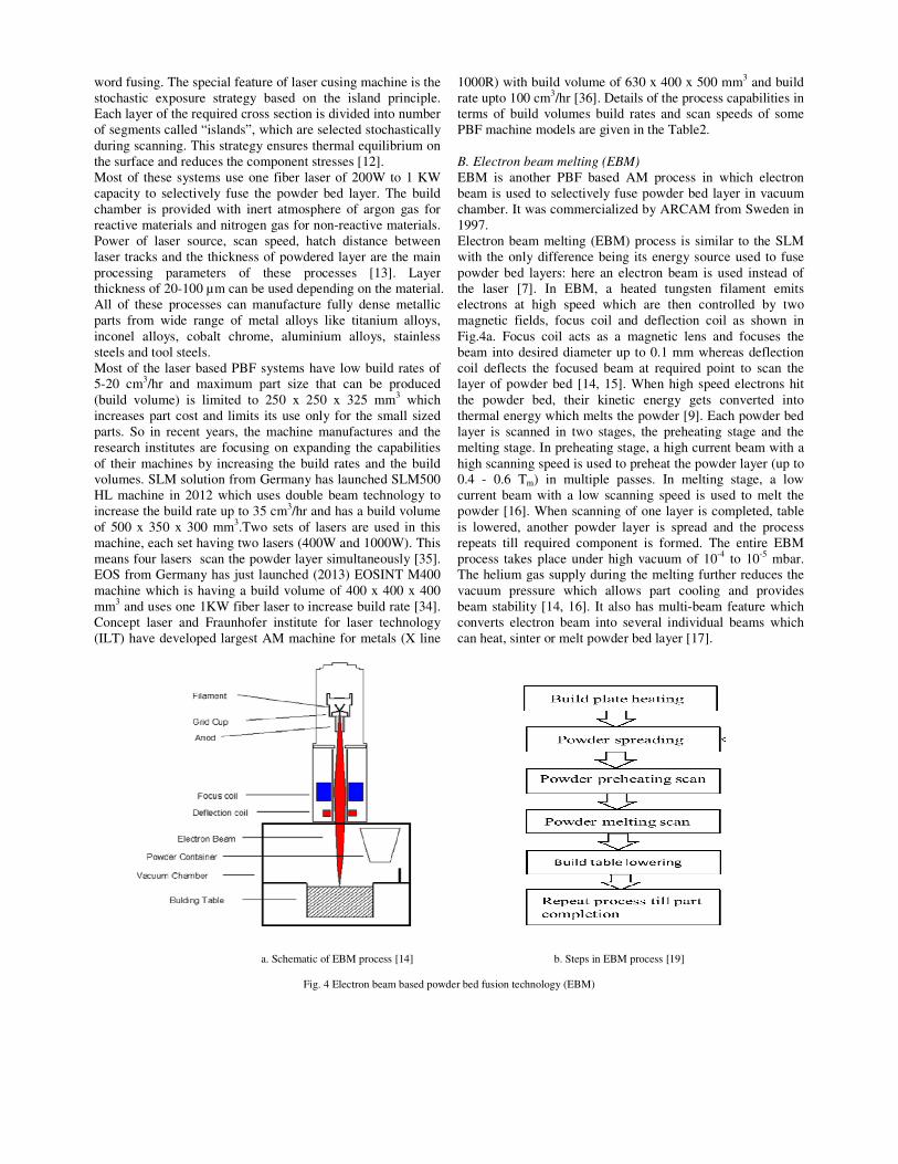
EBM is another PBF based AM process in which electron beam is used to selectively fuse powder bed layer in vacuum chamber. It was commercialized by ARCAM from Sweden in 1997. Electron beam melting (EBM) process is similar to the SLM with the only difference being its energy source used to fuse powder bed layers: here an electron beam is used instead of the laser [7]. In EBM, a heated tungsten filament emits electrons at high speed which are then controlled by two magnetic fields, focus coil and deflection coil as shown in Fig.4a. Focus coil acts as a magnetic lens and focuses the beam into desired diameter up to 0.1 mm whereas deflection coil deflects the focused beam at required point to scan the layer of powder bed [14, 15]. When high speed electrons hit the powder bed, their kinetic energy gets converted into thermal energy which melts the powder [9]. Each powder bed layer is scanned in two stages, the preheating stage and the melting stage. In preheating stage, a high current beam with a high scanning speed is used to preheat the powder layer (up to 0.4 - 0.6 Tm) in multiple passes. In melting stage, a low current beam with a low scanning speed is used to melt the powder [16]. When scanning of one layer is completed, table is lowered, another powder layer is spread and the process repeats till required component is formed. The entire EBM process takes place under high vacuum of 10-4 to 10-5 mbar. The helium gas supply during the melting further reduces the vacuum pressure which allows part cooling and provides beam stability [14, 16]. It also has multi-beam feature which converts electron beam into several individual beams which can heat, sinter or melt powder bed layer [17].
a. Schematic of EBM process [14] b. Steps in EBM process [19]
Fig. 4 Electron beam based powder bed fusion technology (EBM)

ARCAM EBM system uses high power electron beam of 3000 W capacity to melt powder bed layers. Electron beam power, current, diameter of focus, powder pre-heat temperature and layer thickness are main processing parameters of the EBM. Layer thickness of 50-200 µm is typically used in this process [14]. EBM systems can work with wide range of materials like titanium alloys (Ti6Al4V, Ti6Al4V EI), cobalt chrome, Titanium aluminide, inconel (625 and 718), stainless steels, tool steels, copper, aluminium alloys, beryllium etc. [18]
III COMPARISON BETWEEN SLM AND EBM As compared to the SLM system, the EBM has higher build rates (upto 80cm3/hr because of the high energy density and high scanning speeds) but inferior dimensional and surface finish qualities [17]. In both the SLM/EBM process, because of rapid heating and cooling of the powder layer, residual stresses are developed. In EBM, high build chamber temperature (typically 700-9000C) is maintained by preheating the powder bed layer. This preheating reduces the thermal gradient in the powder bed and the scanned layer which reduces residual stresses in the part and eliminates post heat treatment required. Preheating also holds powder particles together which can acts as supports for overhanging structural members. So, supports required in the EBM are only for heat conduction and not for structural support. This reduces the number of supports required and allows manufacturing of more complex geometries. Powder preheating feature is available in very few laser based systems where it is achieved by platform heating. In addition, entire EBM process takes place under vacuum since, it is necessary for the quality of the electron beam [20]. Vacuum environment reduces thermal convection, thermal gradients and contamination and oxidation of parts like titanium alloys [17]. In SLM, part manufacturing takes place under argon gas environment for reactive materials to avoid contamination and oxidation whereas non-reactive materials can be processed under nitrogen environment. So it can be expected that EBM manufactured parts have lower oxygen content than SLM manufactured parts [21]. In spite of having these advantages, EBM is not as popular as SLM because of its higher machine cost, low accuracy and non-availability of large build up volumes. Characteristic features of SLM and EBM are summarized in Table 1.
TABLE I CHARACTERISTIC FEATURES OF SLM AND EBM
SLM EBM
Power source
One or more fiber lasers of 200 to 1000
W
High power Electron beam of
3000 W
Build chamber
environment Argon or Nitrogen
Vacuum / He bleed
Method of powder
preheating Platform heating Preheat scanning
Powder preheating
temperature (0 C) [34,35]
100-200 700-900
Maximum available
build volume (mm) 500 x 350 x 300 350 x 380(ØxH)
Maximum build rate
(cm3/hr) 20-35 80
Layer thickness
(µm) 20-100 50-200
Melt pool size (mm) 0.1-0.5 0.2-1.2
Surface finish [7]
(Ra) 4-11 25-35
Geometric tolerance
(mm) [12] ± 0.05-0.1 ± 0.2
Minimum feature
size(µm) [39] 40-200 100
IV APPLICATIONS OF METAL ADDITIVE MANUFACTURING Metal AM started to gain attention in aerospace, oil and gas, marine, automobile, manufacturing tools and medical applications because of the advantages offered by this process. First, it can reduce buy to fly ratio considerably which is the ratio of input material weight to final part weight. For conventional manufacturing processes, buy to fly ratio for aerospace engine and structural components can be as high as 10 : 1 and 20 : 1 respectively. AM can produce near net shape using layer by layer addition of materials as per requirement which can reduce buy to fly ratio up to 1 : 1 [8,22]. AM can produce highly complex parts and provide freedom in part design. It can be used for structural optimization by using finite element analysis (FEA) to get benefit in terms of light weighting. It can also produce lattice structures with low density, high strength, good energy absorption and good thermal properties which can be used for light weighting and better heat dissipation in applications like heat exchangers in aerospace, automobile and computer industries [23]. Fig. 5 shows conventional and optimized door bracket manufactured by AM where internal ‘bamboo’ structure is used for light-weighting [31].
Fig. 5 Conventional and optimized part by additive manufacturing [31]

Conventionally manufactured part may require a number of different manufacturing processes like casting, rolling, forging, machining, drilling, and welding etc. whereas, same part can be produced by using AM which eliminates required tooling and produces part in single processing step. Every part manufactured by AM can be unique and produced in very short time which enables mass customization [24].
Fig. 6 GE’s additively manufactured fuel nozzle [30]
AM also reduces assembly requirements by integrating number of parts required in assembly into a single part. It reduces overall weight, decreases manufacturing time, reduces number of manufacturing processes required, reduces cost and material requirements and optimizes required mechanical properties [22]. GE has integrated fuel nozzle assembly of 20 small parts into single fuel nozzle part of cobalt chrome material (Fig. 6) which is under testing phase. It is 25 % lighter and five times more durable than conventional assembly [25]. Oak Ridge National Laboratories has manufactured lightweight, compact underwater robotic system (Hydraulic manifold) in which the robot base, hydraulic reservoir, and accumulator are integrated into a single lightweight structure [26].
Fig. 7 Conformal cooling channel insert [33]
AM can enhance part performance and add value to the product as parts can be designed for function. Injection
moulding tools can be provided with conformal cooling channels (Fig. 7) which increases cooling efficiency and reduces the cycle time. Different types of lattice structures can be used to achieve unique properties like improved heat dissipation, structures with negative poisons ratio and improved energy absorption characteristics [22, 27]. A negative poisons ratio increases impact resistance, fracture toughness and shear resistance [14].
Fig. 8 Lattice structure for light weighting [32]
V SUMMARY AND CHALLENGES OF PBF TECHNOLOGIES Though significant progress and technological advancement have been made by the PBF AM technology, performances in terms of speed, accuracy, process control and cost effectiveness still needs to improve. Knowledge of processing-structure-property relationship for existing materials is required to predict part performance. In-process quality monitoring and closed loop control systems are required to improve the consistency, repeatability and uniformity across machines. Closed loop melt pool temperature control system has proven its significance in deposition based LENS (Laser engineered net shaping) process by maintaining desired quality of part. Such close loop melt pool temperature control system has still remained as a challenge for SLM systems. Early stage defect detection through in-process quality monitoring could save required raw material and manufacturing time [28]. Better understandings of physical and metallurgical mechanisms responsible for variation in properties are required for predictive process
modelling. AM part cost is still on the higher side for some applications. Increasing build speeds of AM machines, designing more complex geometries and reducing assembly requirements could reduce required part cost and widen application areas of AM in future.

TABLE II FEATURES OF DIFFERENT PBF BASED AM MACHINES
Manufacturer
Model Energy source Build volume (mm) Build rate
(cm3/hr.)
Scan
speed
(m/s)
EOS [34] EOS M400 1 KW fiber laser 400 x 400 x 400 NA 7
EOS [34] EOS M280 /
M290 200 W or 400 W
fiber laser 250 x 250 x 325 5-20 7
SLM Solution [35] SLM 500HL 2 x 400 W lasers & 2 x 1000 W lasers
(optional) 500 x 280 x 325 Upto 70 Upto 15
SLM Solution [35]
SLM 280 400 W and 1000
W(optional) lasers 280 x 280 x 350 20-35 Upto 15
Concept laser [36] M2 Cusing 200 W (cw) or 400
W (cw) 250 x 250 x 280 2-20
7
Renishaw [37] SLM 250 200 W or 400 W
Fiber laser 250 x 250 x 300 5-20
7
ARCAM [38] Q 10 3000 W electron
beam 200 x 200 x 180 Upto 80
1000 max.
ARCAM [38] Q 20 3000 W electron
beam 350 x 380 mm
(ØxH) Upto 80
1000 max
REFERENCES [1] F-2792- 12a, Standard Terminology for Additive Manufacturing
Technologies
[2] Additive Manufacturing: Pursuing the Promise, advanced
manufacturing office, US Department office, August 2012. [3] T. Wohlers, Wohlers Associates, Inc, Additive Manufacturing
State of the Industry, Wohlers report 2010. [4] Dr. A. Koptyug, Dr. L.E. Rännar, Dr. M. Bäckström, M.Sc. S. F.
Franzén, DDS Dérand, Additive Manufacturing Technology
Applications Targeting Practical Surgery, Sweden, 2013. [5] I. D. Harris, Ph. D.Director, AMC, EWI, Columbus, OH,
Development and Implementation of Metals Additive
Manufacturing. [6] B. Stucker, University of Louisville, Additive Manufacturing
Technologies: Technology Introduction and Business Implications.
[7] B. Vayre, Frederic Vignat and Francois Villeneuve, Metallic
additive manufacturing: State-of-the-art review and prospects,
Grenoble, France, January 2012. [8] C. L. English, S. K. Tewari, and D. H. Abbott, An Overview of Ni
Base Additive Fabrication Technologies For Aerospace
Applications (Preprint), GE Aviation, March 2011. [9] J. Ruan, T. E. Sparks, Z. Fan, J. K. Stroble, A. Panackal and F.
Liou, A Review of Layer Based Manufacturing Processes for Metals,Department of Mechanical and Aerospace Engineering, University of Missouri – Rolla.
[10] M. Shellabear, O. Nyrhilä, DMLS – Development History And
State Of The Art, 1EOS GmbH Electro Optical Systems, Germany; 2EOS Finland, Finland.
[11] D. Thomas, The Development of Design Rules for Selective Laser
Melting, Ph. D Thesis, University of Wales Institute, Cardiff, October 2009.
[12] M. Aliakbari, Additive Manufacturing: State-of-the-Art,
Capabilities, and Sample Applications with Cost Analysis, Master of Science Thesis, Department of Industrial Production, KTH, June 2012.
[13] A.B. Spierings, K. Wegener, G. Levy, Designing Material
Properties Locally with Additive Manufacturing technology SLM,
INSPIRE AG –institute for rapid product development irpd, Lerchenfeldstrasse 5, CH- 9014 St.Gallen, Switzerland, 2012.
[14] X. Gong, Ted Anderson and Kevin Chou, Review on Powder-
Based Electron Beam Additive Manufacturing Technology,
Mechanical Engineering Department The University of Alabama Tuscaloosa, June 2012.
[15] J. Hiemenz, EBM Offers a New Alternative For Producing
Titanium Parts And Prototypes, Time-Compression Technologies, June 2006.
[16] L. E. Murr, E. Martinez, K. N. Amato, S. M. Gaytan, J. Hernandez, D. A. Ramirez, P. W. Shindo, F. Medina, R. B. Wicker, Fabrication of Metal and Alloy Components by Additive
Manufacturing: Examples of 3D Materials Science,Department of Metallurgical and Materials Engineering, The University of Texas at El Paso, El Paso, TX 79968 USA, 2012.

[17] B. Vayre , F. Vignat, F. Villeneuve, Identification on some design
key parameters for Additive manufacturing: application on
Electron Beam Melting, Forty Sixth CIRP, Conference on Manufacturing Systems, 2013.
[18] R. Udroiu, Powder Bed Additive nufacturing Systems and its
Applications, Academic Journal Of Manufacturing Engineering, Vol. 10,Issue 4/2012.
[19] J. Wooten, D. P. Dennies, Electron Beam Melting Manufacturing
for Production Hardware, SAE International, 2008. [20] M. Koikea, K. Martineza, L. Guoa, G. Chahine, R. Kovacevic, T.
Okabe, Evaluation Of Titanium Alloy Fabricated Using Electron
Beam Melting System For dental Applications, Journal of Materials Processing Technology, 2011.
[21] L. Loeber, S. Biamino, U. Ackelid, S. Sabbadini, P. Epicoco, P. Fino, J. Eckert, Comparison of Selective Laser And Electron Beam
Melted Titanium Aluminides, Leibniz Institute for Solid State and Materials Research Dresden.
[22] Horn, T. J.Harrysson, Ola L.A., Overview of Current Additive
Manufacturing Technologies and Selected applications,
Science Reviews 2000 Ltd, 2012. [23] S. L. Campanelli, N. Contuzzi, A. Angelastro and A. D. Ludovico,
Capabilities and Performances of the Selective Laser Melting
Process,Department of Management and Mechanical Engineering, Viale Japigia,182,Italy, 2010.
[24] J. Geraedts, E. Doubrovski, J. Verlinden, M. Stellingwerff, Three
Views On Additive Manufacturing: Business, Research, And
Education, Proceedings of TMCE, 2012. [25] MIT Technology Review, 2013 Breakthrough Technology:
Additive Manufacturing, 2013. [26] T. Wohlers, Additive Manufacturing at Work,
www.sme.org/manufacturingengineering, April 2012. [27] M. Thymianidis, C. Achillas, D. Tzetzis, E. Iakovou, Modern
Additive Manufacturing Technologies: An Upto- Date Synthesis
and Impact on Supply Chain Design, School of Economics and Business Administration, International Hellenic University, Thermi, Greece.
[28] J. Scott, N. Gupta, C. Weber, S. Newsome, Additive
Manufacturing: Status and Opportunities, Wohlers Associates, Inc, March 2012.
[29] E. C. Santosa, M. Shiomia,_, K. Osakadaa, T. Laoui, Rapid
manufacturing of metal components by laser forming, Department of Mechanical Science and Bioengineering, Osaka University, Machikaneyama, Toyonaka, Osaka 560-8531, Japan.
[30] GE capital, Additive Manufacturing Redefining What’s Possible,
Fall 2013. QMISOLUTIONS, Additive manufacturing, white paper, January 2013.
[31] QMISOLUTIONS, Additive Manufacturin, , January 2013. [32] J. V. Vaerenbergh, Phd, L. Thijs, Phd, W. V. der Perre, Msc., and
T. D. Bruyne, Msc, Application Specific AM Technology
Development for High-End Mechatronic Systems, LayerWise NVLeuven, Belgium.
[33] S. Kumar, S. Pityana, Laser-Based Additive Manufacturing of
Metals, Council for Scientific and Industrial Research, National Laser Centre, Pretoria 0001, South Africa.
[34] (2014) EOS website [online], available at www. eos.info,accessed April 2014.
[35] (2014) SLM Solution website [online], available at www.slm-solution.com, accessed April 2014.
[36] (2014) Concept Laser website [online], available at www.concept-laser.de, accessed April 2014.
[37] (2014) Renishaw website [online], available at www.renishaw.co.in, accessed April 2014.
[38] (2014) Arcam website [online], available at www.arcam.com, accessed April 2014.
[39] (2014) additively website [online], available at www.additively.com, accessed April 2014.
Abbreviations The following symbols are used in this paper. AM: Additive manufacturing PBF: Powder bed fusion DED: Directed energy deposition SLS: Selective laser sintering DMLS: Direct metal laser sintering SLM: Selective laser melting EBM: Electron beam melting LENS: Laser engineered net shaping DMD: Direct metal deposition EBFFF: Electron beam free form fabrication CAD: Computer aided design