
Review on Lecture-1teacher.buet.ac.bd/lutfulkabir/ICT6641_April2011/Lecture_2.pdf · Review on...
23
1 Lecture 2 Branch, Call and Delay Loops, AVR I/O port programming Prof. S. M. Lutful Kabir IICT, BUET Session: April, 2011 ICT 6641: Advanced Embedded System IICT, BUET Review on Lecture-1 • Three parts of a computer : CPU, Memory and I/O • Instruction execution • Types of memory – • ROM : PROM, EPROM, EEPROM, Flash ROMmMask ROM • RAM : SRAM, NVRAM, DRAM • Microcontroller versus Microprocessor • Application of microcontrollers • Embedded Systems & their design challenges • AVR microcontroller • AVR family overview
Transcript of Review on Lecture-1teacher.buet.ac.bd/lutfulkabir/ICT6641_April2011/Lecture_2.pdf · Review on...

1
Lecture 2
Branch, Call and Delay Loops,
AVR I/O port programming
Prof. S. M. Lutful Kabir
IICT, BUET
Session: April, 2011
ICT 6641: Advanced Embedded System
IICT, BUET
Review on Lecture-1
• Three parts of a computer : CPU, Memory and I/O
• Instruction execution
• Types of memory –
• ROM : PROM, EPROM, EEPROM, Flash ROMm Mask ROM
• RAM : SRAM, NVRAM, DRAM
• Microcontroller versus Microprocessor
• Application of microcontrollers
• Embedded Systems & their design challenges
• AVR microcontroller
• AVR family overview

2
IICT, BUET
Review on Lecture-1 (continued)
• AVR features
• General purpose AVR registers
• Types of memory in AVR microcontroller
• LDI, ADD, LDS, STS, IN, OUT, MOV instructions
• AVR status register
• AVR Assembly language programming
• The program counter
• Harvard’s Architecture in AVR
• RISC Architecture in AVR
IICT, BUET
Branching and Looping
•BRNE Instruction for looping
Back: …………………. ; start of the loop
…………………. ; body of the loop
DEC Rn ; decrement Rn, Z=1 when Rn=0
BRNE Back ; branch to Back if Z=0
– the Rn is decremented; if it is not zero, it branches (jumps)
back to the target address referred by the label.
– Prior to the start of the loop, the Rn is loaded with the
counter value for the number of repetitions.
– Notice that BRNE instruction refers to the Z flag of the status
register affected by the previous instruction, DEC

3
IICT, BUET
An Example Program for Branching
• Write a program to clear R20 and then add 3 to R20 ten times and finally send the sum to PORTB
; this program adds the value 3 to R20 ten times
.INCLUDE “M32DEF.INC”
LDI R16, 10
LDI R20, 0
LDI R21, 3
AGAIN : ADD R20, R21
DEC R16
BRNE AGAIN
OUT PORTB, R20
Load Counter with 10
Clear R20
Load R21 with 3
ADD Value
Place result on port
Decrement Counter
Is Counter Zero?
IICT, BUET
Loop inside loop
• Write a program to (a) load the PORTB with the value 0x55, and (b) complement Port B 700 times
.INCLUDE “M32DEF.INC”
.ORG 0
LDI R16, 0x55
OUT PORTB, R16
LDI R20, 10
LOP_1: LDI R21, 70
LOP_2: COM R16
OUT PORTB, R16
DEC R21
BRNE LOP_2
DEC R20
BRNE LOP_1

4
IICT, BUET
Other Conditional Branch (Jump)
INSTRUCTION ACTION
BRLO Branch if C=1
BRSH Branch if C=0
BREQ Branch if Z=1
BRNE Branch if Z=0
BRMI Branch if N=1
BRPL Branch if N=0
BRVS Branch if V=1
BRVC Branch if V=0
IICT, BUET
All conditional branches are short
jumps
• Short jumps means that the address of the target must be
within 64 bytes of the program counter (PC)
PC
+1
OPCODE(pt1) OPCODE(pt2)
15 10 9 3 2 0
15 0

5
IICT, BUET
An Example of backward jump
LINE ADDRESS Machine Mnemonics Operand
3: +00000000: E00A LDI R16, 10
4: +00000001: E040 LDI R20, 0
5: +00000002: E053 LDI R21, 3
6: +00000003: 0F45 AGAIN: ADD R20, R21
7: +00000004: 950A DEC R16
8: +00000005: F7E9 BRNE AGAIN
9: +00000006: BB48 OUT PORTB, R20
BRNE AGAIN has the machine code of F7E9. Its binary equivalent is 1111011111101001
The mnemonics is from 15-9 & 2-0, i.e., 111101001 and the operand is the binary underlined, i.e., 1111101. It gives -3.
Since previous PC=5, so new PC=+5+1-3=3 and the address of label “AGAIN” is 3
IICT, BUET
Unconditional Jump
• The unconditional jump is a jump in which control is
transferred unconditionally to the target location
• In AVR there are three unconditional branches
– JMP (jump)
– RJMP (relative jump)
– IJMP (Indirect jump)
• JMP (JMP is a long jump)
– Can go to any memory location in the program ROM space
– The instruction is a 4 byte instruction and has the format of
1 0 0 1 0 1 0 k21 k20 … k17 1 1 0 k16 k15………… .. k8 k7 ..................... k0
8 bit 8 bit 8 bit 8 bit

6
IICT, BUET
RJMP (Relative Jump)
• This is a 2-byte instruction, first 4 bits are opcode and lower
12 bits are relative address ranging from 0x000-0xFFF
• The relative address is divided into forward and backward
jumps; i.e., within -2048 to +2047 words of memory relative
to current PC
• In conditional jump the relative address is of 7 bit and in RJMP
it is 12 bit
• Since this is a 2-byte instruction so it is preferred than JMP
• Its format is:1100 kkkk kkkk kkkk
IICT, BUET
IJMP (Indirect Jump)
• IJMP is a 2-byte instruction
• When the instruction executes the PC is loaded with the
content of Z-register, so it jumps to the address pointed to by
the Z-register [Z is a two byte register, will be discussed later]
• So, IJMP can jump within the lowest 64K words of the
program memory
• In other jump instructions, the target address is static which
means that in a specific condition they jump to a fixed point
• But, IJMP has a dynamic target point and we can dynamically
change the target address by changing the Z register’s
contents through the program

7
IICT, BUET
CALL Instructions and Stack
• CALL is used for calling a subroutine whereas subroutine is
used for performing a task that need to be performed
repeatedly
• In AVR, there are four instructions for the call subroutine,
namely CALL (long call), RCALL (relative call), ICALL (indirect
call to Z) and EICALL (extended indirect call to Z)
• CALL (long call) Instruction
– This is a 4 byte instruction, 10 bits are used for the opcode and rest 22
bits for the address of the target subroutine
– Therefore, CALL can be used to call subroutines located anywhere
within the 4M address space 0x000000-0x3FFFFF
– The instruction format is similar to JMP instruction
IICT, BUET
Stack and Stack Pointer
• The stack is a section of RAM used by the CPU to store
information temporarily
• The information could be data or address
• The register used to access the stack is called SP (Stack
Pointer) register [consisting of SPL, SPH]
• The storing of CPU information such as the program counter
on the stack is called a PUSH, and loading of stack contents
back to a CPU register is called a POP
• The SP points to the top of the stack. As we push data onto a
stack the data are saved where SP points to and the SP is
decremented by one
8
IICT, BUET
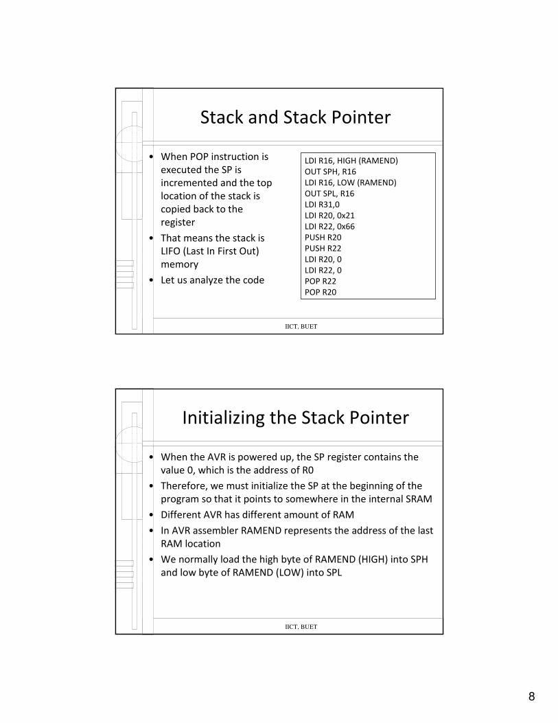
Stack and Stack Pointer
• When POP instruction is
executed the SP is
incremented and the top
location of the stack is
copied back to the
register
• That means the stack is
LIFO (Last In First Out)
memory
• Let us analyze the code
LDI R16, HIGH (RAMEND)
OUT SPH, R16
LDI R16, LOW (RAMEND)
OUT SPL, R16
LDI R31,0
LDI R20, 0x21
LDI R22, 0x66
PUSH R20
PUSH R22
LDI R20, 0
LDI R22, 0
POP R22
POP R20
IICT, BUET
Initializing the Stack Pointer
• When the AVR is powered up, the SP register contains the
value 0, which is the address of R0
• Therefore, we must initialize the SP at the beginning of the
program so that it points to somewhere in the internal SRAM
• Different AVR has different amount of RAM
• In AVR assembler RAMEND represents the address of the last
RAM location
• We normally load the high byte of RAMEND (HIGH) into SPH
and low byte of RAMEND (LOW) into SPL

9
IICT, BUET
CALL Instruction and the role of the
stack
• When a subroutine is called, the processor first saves the
address of the instruction just below the CALL instruction on
the stack and then transfer control to the subroutine
• This is how the CPU knows where to resume when it returns
from the called subroutine
• For AVRs whose program counter is not longer than 16 bits
(e.g. ATmega128, ATmega32), the value of the program
counter is broken into 2 bytes. The higher byte is pushed onto
the stack first and then the lower byte is pushed
• For AVRs whose program counter is longer than 16 bits but
shorter than 24 bits, it is broken in 3 bytes and the push
sequences is higher, middle and lower byte one after another
IICT, BUET
RET Instruction and the role of the
stack
To understand the role of stack during RET instruction let us
follow the program for Toggling all bits of PortB by sending to
it the values 0x55 and 0xAA continuously. Put a time delay
between each issuing of data to PortB
BACK:
LDI R16, 0x55
OUT PORTB, R16
CALL DELAY
LDI R16, 0xAA
OUT PORTB, R16
CALL DELAY
RJMP BACK
.ORG 0x300DELAY:
LDI R20, 0XFFAGAIN:
NOPNOPDEC R20BRNE AGAINRET
main subroutine
10
IICT, BUET
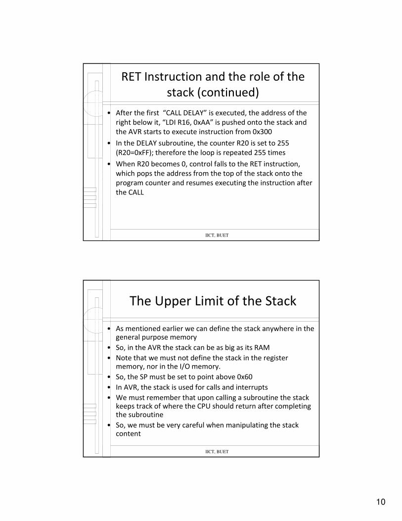
RET Instruction and the role of the
stack (continued)
• After the first “CALL DELAY” is executed, the address of the
right below it, “LDI R16, 0xAA” is pushed onto the stack and
the AVR starts to execute instruction from 0x300
• In the DELAY subroutine, the counter R20 is set to 255
(R20=0xFF); therefore the loop is repeated 255 times
• When R20 becomes 0, control falls to the RET instruction,
which pops the address from the top of the stack onto the
program counter and resumes executing the instruction after
the CALL
IICT, BUET
The Upper Limit of the Stack
• As mentioned earlier we can define the stack anywhere in the general purpose memory
• So, in the AVR the stack can be as big as its RAM
• Note that we must not define the stack in the register memory, nor in the I/O memory.
• So, the SP must be set to point above 0x60
• In AVR, the stack is used for calls and interrupts
• We must remember that upon calling a subroutine the stack keeps track of where the CPU should return after completing the subroutine
• So, we must be very careful when manipulating the stack content

11
IICT, BUET
Calling a subroutine from another subroutine
which is called from the main program
Write a program to count up from 0x00 to 0xFF and send the
count to PORTB. Use one subroutine for sending the data to
PORTB and another one for time delay
LDI COUNT, 0
BACK:
CALL DISPLAY
RJMP BACK
.ORG 0x300DELAY:
LDI R20, 0XFFAGAIN:
NOPNOPDEC R20BRNE AGAINRET
DISPLAY:
INC COUNT
OUT PORTB, COUNT
CALL DELAY
RET
DISPLAY SUBDELAY SUB
MAIN
IICT, BUET
Calling a subroutine from another subroutine
which is called from the main program (contd.)
• The address of the instruction “CALL DISPLAY” is 0x0007 and
that after “CALL DELAY” is 0x000C
• So, the SP will move as shown in the following figure
85B
85C
85D
85F SP
Before CALL
DISPLAY
SP
After CALL
DISPLAY
SP
After CALL
DELAY
SP
After DELAY
RET
SP
After DISPLAY
RET
00
07
00
07
00
0C
00
07

12
IICT, BUET
ICALL (Indirect CALL)
• In this 2-byte (16 bit) instruction, the Z register specifies the target address
• When the instruction is executed the address of the next instruction is pushed into the stack (like CALL and RCALL) and the program counter is loaded with the content of Z register
• So Z register should contain the address of the function when the ICALL instruction is executed
• In AVRs with more than 64K words of program memory the EICALL (extended indirect call) instruction is available
• The EICALL loads the Z register into the lower 16 bits of the PCand the EIND register into the upper 6 bits of the PC
• Notice that EIND is a part of I/O memory
IICT, BUET
Pipelining
• In early microprocessor such as 8085, the CPU could either
fetch or execute at a given time
• In other words, the CPU had to fetch an instruction from
memory, then execute it and then fetch the next instruction,
execute it and so on
• The idea of pipelining in its simplest form is to allow the CPU
to fetch and execute at the same time (an instruction fetches
while the previous instruction executes)
• The diagram in the next slide demonstrate the situation

13
IICT, BUET
Pipelining (continued)
fetch 1 fetch 2 fetch 3exec 1 exec 2 exec 3
fetch 1
fetch 2
fetch 3
fetch 4
fetch 5
exec 1
exec 2
exec 3
exec 4
exec 5
T1 T2 T3 T4 T5 T6
Non pipeline
Pipeline
IICT, BUET
Instruction cycle time for the AVR
• It takes certain amount of time for the CPU to execute an
instruction
• This time is referred to as machine cycles
• Because all the instructions in the AVR are either 1-word (2-
byte) or 2-word (4-byte), most instruction takes more than 1
or 2 machine cycles to execute
• Note that some instruction like JMP or CALL takes three or
four machine cycles
• In the AVR, one machine cycle consists of one oscillator
period

14
IICT, BUET
Branch penalty
• The simultaneous operation of execute and fetch is
maintained by a process called queuing
• In some circumstances, CPU must flush out the queue
• For example, when a branch instruction is executed the CPU
starts to fetch from a new memory location and the code in
the queue that was fetched previously is discarded
• In this case, the execution unit must wait until fetch unit
fetches the new instruction
• This is called a branch penalty
• It happens in case of JMP, CALL, RET and all conditional
branch instruction
IICT, BUET
Calculation of delay time
InstructionCycle
.DEF COUNT = R20 0 DELAY: LDI COUNT, 0xFF 1AGAIN: NOP 1
NOP 1DEC COUNT 1BRNE AGAIN 2/1RET 4
Therefore, we have a time delay of [1+((1+1+1+2)X255)+4] x 0.1 uS = 128 uS
Notice that BRNE takes two instruction cycles if it jumps back and takes only one machine cycle when falling through the loop. That means the above number should be 127.9 uS.

15
IICT, BUET
AVR I/O Programming
• In AVR family, there are
many ports for I/O
operations, depending on
which family member you
choose
• In ATmega32 chip there are
in total 40 pins of which 32
pins are for four ports
namely PORTA, PORTB,
PORTC and PORTD
12
3
6
9
12
15
18
20
4039
38
35
32
29
26
23
21
45
7
8
10
11
13
14
16
17
19 22
24
25
2728
30
31
33
34
36
37
(XCK/T0) PB0(T1) PB1
(INT2/AINO) PB2
(OCO/AIN1) PB3
(SS) PB4(MOSI) PB5
(MIS0) PB6
(SCK) PB7
RESET
VCC
GNDXTAL2
XTAL1
(RXD) PD0
(TXD) PD1(INT0) PD2(INT1) PD3
(OC1B) PD4
(OC1A) PD5(ICP) PD6 PD7 (OC2)
PC0 (SCL)
PC1 (SDA)PC2 (TCK)
PC3 (TMS)
PC4 (TD0)
PC5 (TDI)
PA0 (ADC0)
PC6 (TOSC1)PC7 (TOSC0)
AVCCAGND
AREF
PA1 (ADC1)
PA2 (ADC2)
PA3 (ADC3)
PA4 (ADC4)PA5 (ADC5)
PA7 (ADC7)PA6 (ADC6)
AT
meg
a
32
IICT, BUET
I/O port pins and their functions
• The number of ports in the AVR family varies depending on
the number of pins on the chip
• The 8-pin AVR has port B only while the 64-pin version has
ports A through F and 100-pin AVR has ports A through L
• To use any of these ports as an input or output port, it must
be programmed
• In addition to being used as simple I/O, each port has some
other functions such as ADC, timers, interrupts, and serial
communication pins
• Not all ports has 8 pins. For example, in ATmega8 PORTC has
7 pins.

16
IICT, BUET
I/O port pins and their functions
(continued)
• Each port has three I/O registers associated with it as shown in the figure below
• DDR stands for Data Direction Register, PIN stands for Port Input pins
DDRx
PORTx
PINx
7 6 5 4 3 2 1 0
7 6 5 4 3 2 1 0
7 6 5 4 3 2 1 0
Px7 Px6 Px5 Px4 Px3 Px2 Px1 Px0
IICT, BUET
The role of DDRx Register
• The DDRx I/O register is used solely for the purpose of making a given port an input or output port
• For example, to make a port an output, we write 1s to the DDRx register
• Similarly to make a port an input, we write 0s to the DDRxregister
• The following program toggles all 8 bits of Port B
LDI R16, 0xFF CALL DELAY
OUT DDRB, R16 LDI R16, 0XAA
L1: LDI R16, 0x55 OUT PORTB, R16
OUT PORTB, R16 CALL DELAY
RJMP L1

17
IICT, BUET
Outputting Data to Port
• In the previous example, the data is sent to PortB by simply
sending data to PORTB register
OUT PORTB, R16
• The only thing to remember is that corresponding DDRB must
be configured before data is sent to the particular port
IICT, BUET
To read data from a PORT as input
• The following code gets that data present at the pins of port C
and send it to port B indefinitely, after adding 5 to it
.INCLUDE “M32DEF.INC” L2: IN R16, PINC
LDI R16, 0x00 LDI R17,5
OUT DDRC, R16 ADD R16, R17
LDI R16, 0xFF OUT PORTB, R16
OUT DDRB, R16 RJMP L2
• In the above program 0s is send to DDRC, so Port C becomes
an input port and 1s to DDRB, so Port B becomes output port

18
IICT, BUET
Using built-in pull-up resistors with
the input pins
• There is a pull-up resistor for each of the AVR pins
• If we put 1s into bits of the PORTxregister, the pull-up resistors are activated
• The advantage of connecting pull-up resistor is that if nothing is connected to the corresponding pin it stays at high impedance because the resistor pulls it up
• If we put 0s into the bits of PORTxregister, the pull-up resistor is inactive
PINx.n
VCC
PORTx.n
1=Close
0=Open
pin n of
Port x
Outside
of AVR
Inside of
AVR
LDI R16, 0xFFOUT PORTC, R16LDI R16, 0x00OUT DDRC, R16
IICT, BUET
States of a Port
Out 1Input and Pull-
up
1
Out 0Input and high
Impedance
0
10DDRx
PORTx

19
IICT, BUET
Dual Role of Port A and Port B
• The AVR multiplexes an analog-to-digital converter through port A to save
I/O pins. The alternative functions of the pins for port A are shown in the
following table
• AVR multiplexes with some other functions through port B
ADC7PA7
ADC6PA6
ADC5PA5
ADC4PA4
ADC3PA3
ADC2PA2
ADC1PA1
ADC0PA0
FunctionsBit
SCKPB7
MISOPB6
MOSIPB5
SSPB4
OC0/AIN1PB3
INT2/AIN0PB2
T1PB1
XCK/T0PB0
FunctionsBit
IICT, BUET
Dual Role of Port C and Port D
• The alternate functions of Port C and D are shown in the table
below
TOSC2PC7
TOSC1PC6
TD1PC5
TD0PC4
TMSPC3
TCKPC2
SDAPC1
SCLPC0
FunctionsBit
PSP7/P1DPD7
PSP6/P1CPD6
PSP5/P1BPD5
PSP4/ECCP1/P1APD4
PSP3/C21N-PD3
PSP2/C21N+PD2
PSP1/C11N+PD1
PSPO/C11N+PD0
FunctionsBit

20
IICT, BUET
I/O Bit Manipulation Programming
• Sometime of we need to access only 1 or 2 bits of the port instead of the
entire 8 bits
• A powerful feature is the of AVR I/O ports is their capability to access
individual bits of the port without altering the rest of the bits in that port
• Table below lists the single-bit instructions for AVR
Skip if bit in I/O register SetSBIS ioReg, bit
Skip if bit in I/O register ClearedSBIC ioReg, bit
Clear bit in I/O registerCBI ioReg, bit
Set bit in I/O registerSBI ioReg, bit
FunctionsInstructions
IICT, BUET
I/O Registers
• Tables below shows the lower 32 I/O registers
EEARH1F3F
EEARL1E3E
EEDR1D3D
EECR1C3C
PORTA1B3B
DDRA1A3A
PINA1939
PORTB1838
DDRB1737
PINB1636
I/OMemName
Address
UCSRB0A2A
UBRRL0929
ACSR0828
ADMUX0727
ADCSRA0626
ADCH0525
ADCL0424
TWDR0323
TWAR0222
TWSR0121
TWBR0020
I/OMemName
Address
PORTC1535
DDRC1434
PINC1333
PORTD1232
DDRD1131
PIND1030
SPDR0F2F
SPSR0E2E
SPCR0D2D
UDR0C2C
UCSRA0B2B
I/OMemName
Address

21
IICT, BUET
SBI & CBI (Set/Clear bit in I/O register)
• To set HIGH a single bit of a given I/O register, we use the
following syntax
• SBI ioReg, bit_num
• Similar instruction format is for CBI :– CBI ioReg, bit_num
SBI a, b
CBI a, b
0 < a < 31
0 < b < 7
1001 1010 aaaa abbb
1001 1000 aaaa abbb
IICT, BUET
Single bit addressability of Ports
D7PD7PC7PB7PA7
D6PD6PC6PB6PA6
D5PD5PC5PB5PA5
D4PD4PC4PB4PA4
D3PD3PC3PB3PA3
D2PD2PC2PB2PA2
D1PD1PC1PB1PA1
D0PD0PC0PB0PA0
Port BitPORTDPORTCPORTBPORTA

22
IICT, BUET
Checking an input pin
• To make decisions based on the status of a given bit in the file
register, we use the
– SBIC (Skip if bit in I/O register Cleared) and
– SBIS (Skip if bit in I/O register Set) instructions
• These single-bit instructions are widely used for I/O
operations.
• They allow you to monitor a single pin and make a decision
depending on whether it is 0 or 1
• Note that SBIC and SBIS can be used for any of the lower 32
I/O registers including I/O Ports A, B, C, D and so on
IICT, BUET
Format of SBIC and SBIS
SBIC a, b
SBIS a, b
0 < a < 31
0 < b < 7
1001 1011 aaaa abbb
1001 1001 aaaa abbb

23
IICT, BUET
An example use of SBIC
• A switch is connected to pin PB0. Write a program to get the status of SW and save it in location
.EQU MYTEMP = 0x200
.INCLUDE “M32DEF.INC”
CBI DDRB, 0
AGAIN : SBIC PINB, 0
RJMP OVER
LDI R16, 0
STS MYTEMP, R16
RJMP AGAIN
OVER: LDI R16,0x1
STS MYTEMP, R16
RJMP AGAIN
IICT, BUET
End of Lecture 2


