Resonant Tunneling Devices: physics, technology and ... · Resonant Tunneling Devices: physics,...
53
# 1/53 A. Cidronali, Dept. Electronics and Telecommunications, University of Florence – Italy Resonant Tunneling Devices: physics, technology and applications Alessandro Cidronali Dept. Electronics and Telecomm. Univ. of Florence
Transcript of Resonant Tunneling Devices: physics, technology and ... · Resonant Tunneling Devices: physics,...
# 1/53A. Cidronali, Dept. Electronics and Telecommunications, University of Florence – Italy
Resonant Tunneling Devices: physics, technology and
applications
Alessandro CidronaliDept. Electronics and Telecomm. Univ. of
Florence

# 2/53A. Cidronali, Dept. Electronics and Telecommunications, University of Florence – Italy 6/29/2005
Outline
• motivations
• RTD basics
• RTDs physics and models
• Applications
Exploitation of the NDR
Digital applications (gate logic, memory)
# 3/53A. Cidronali, Dept. Electronics and Telecommunications, University of Florence – Italy 6/29/2005
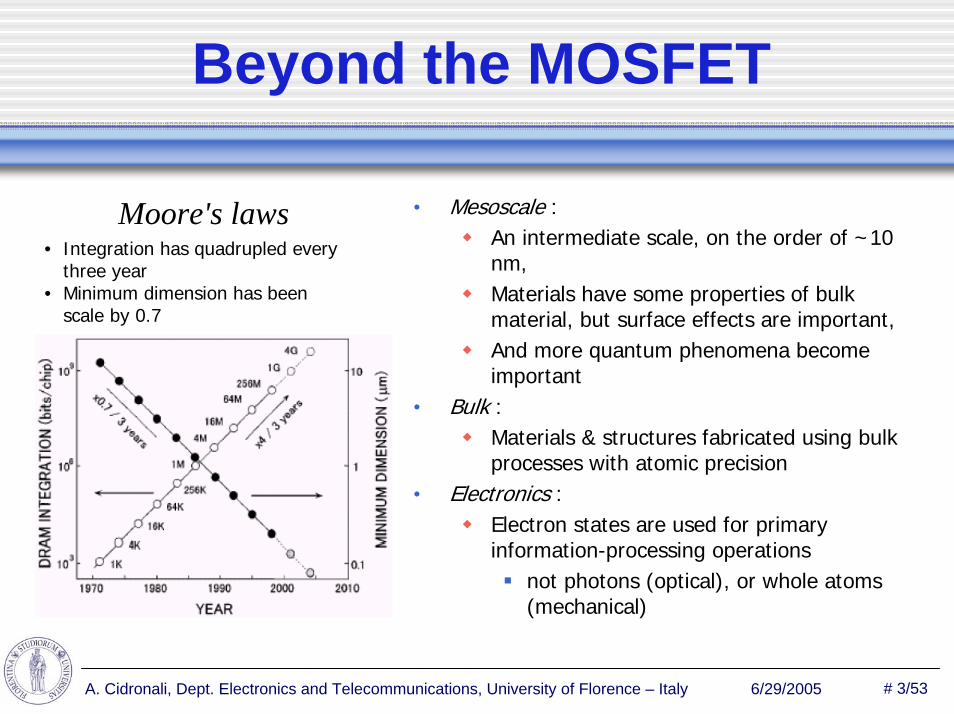
Beyond the MOSFET
• Mesoscale :An intermediate scale, on the order of ~10 nm, Materials have some properties of bulk material, but surface effects are important,And more quantum phenomena become important
• Bulk :Materials & structures fabricated using bulk processes with atomic precision
• Electronics :Electron states are used for primary information-processing operations
not photons (optical), or whole atoms (mechanical)
Moore's laws • Integration has quadrupled every
three year• Minimum dimension has been
scale by 0.7
# 4/53A. Cidronali, Dept. Electronics and Telecommunications, University of Florence – Italy 6/29/2005
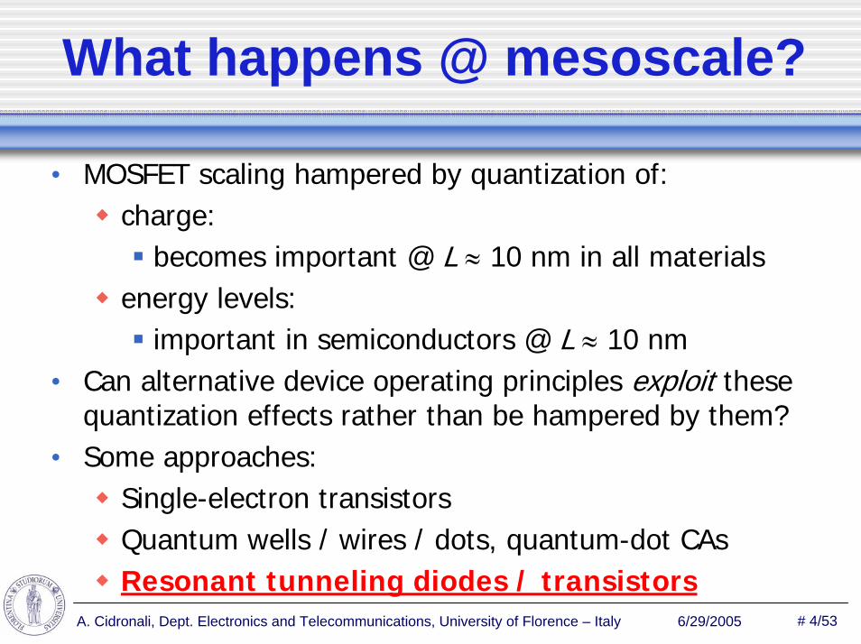
What happens @ mesoscale?
• MOSFET scaling hampered by quantization of:charge:
becomes important @ L ≈ 10 nm in all materialsenergy levels:
important in semiconductors @ L ≈ 10 nm• Can alternative device operating principles exploit these
quantization effects rather than be hampered by them?• Some approaches:
Single-electron transistorsQuantum wells / wires / dots, quantum-dot CAsResonant tunneling diodes / transistors
# 5/53A. Cidronali, Dept. Electronics and Telecommunications, University of Florence – Italy 6/29/2005
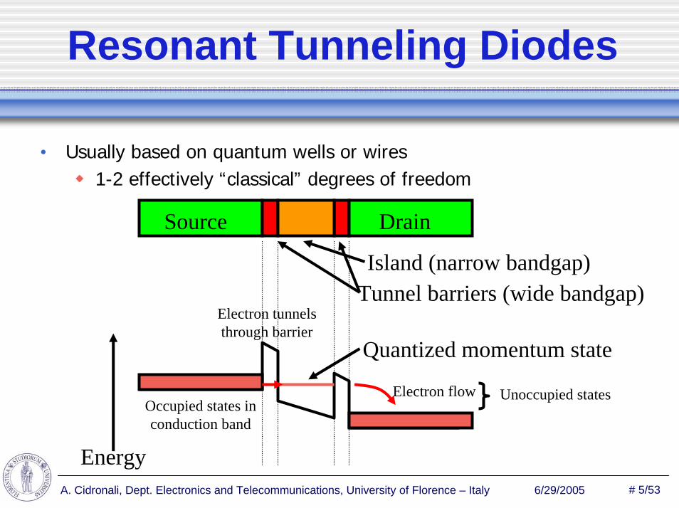
Resonant Tunneling Diodes
• Usually based on quantum wells or wires1-2 effectively “classical” degrees of freedom
Source Drain
Island (narrow bandgap)Tunnel barriers (wide bandgap)
Occupied states inconduction band
Energy
Quantized momentum state
Electron tunnelsthrough barrier
Electron flow Unoccupied states
# 6/53A. Cidronali, Dept. Electronics and Telecommunications, University of Florence – Italy 6/29/2005
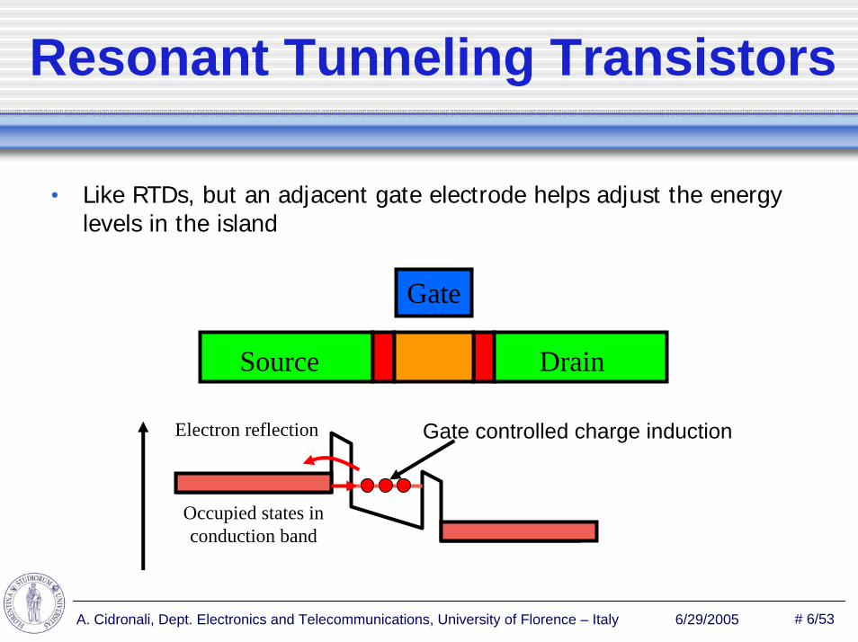
Resonant Tunneling Transistors
• Like RTDs, but an adjacent gate electrode helps adjust the energy levels in the island
Gate
Source Drain
Occupied states inconduction band
Gate controlled charge inductionElectron reflection
# 7/53A. Cidronali, Dept. Electronics and Telecommunications, University of Florence – Italy 6/29/2005
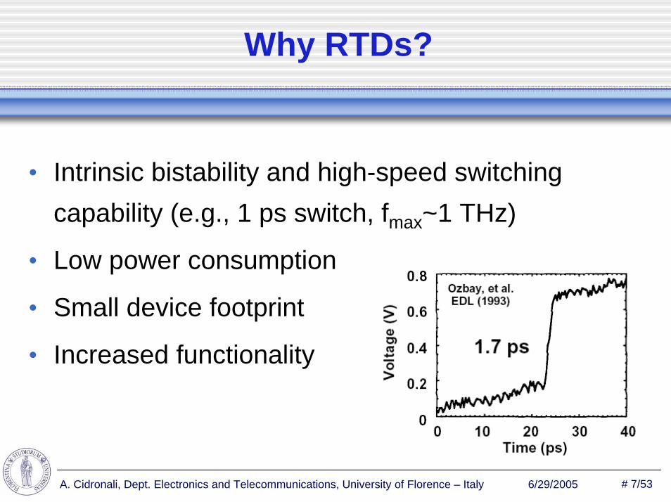
Why RTDs?
• Intrinsic bistability and high-speed switching capability (e.g., 1 ps switch, fmax~1 THz)
• Low power consumption
• Small device footprint
• Increased functionality
# 8/53A. Cidronali, Dept. Electronics and Telecommunications, University of Florence – Italy 6/29/2005
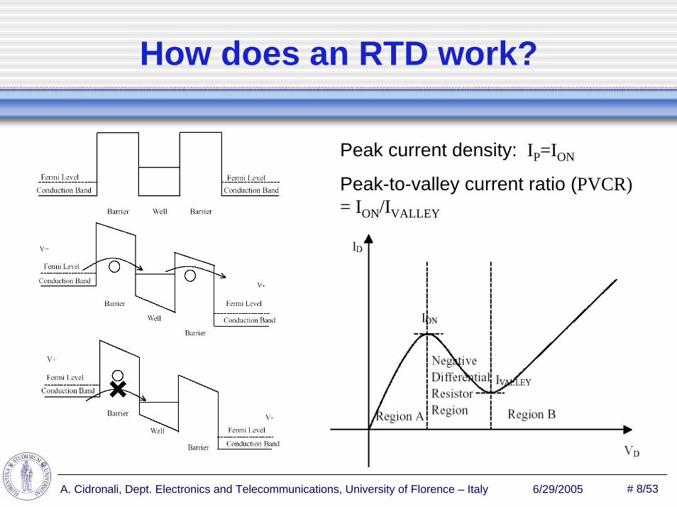
How does an RTD work?
Peak current density: IP=ION
Peak-to-valley current ratio (PVCR)= ION/IVALLEY
# 9/53A. Cidronali, Dept. Electronics and Telecommunications, University of Florence – Italy 6/29/2005
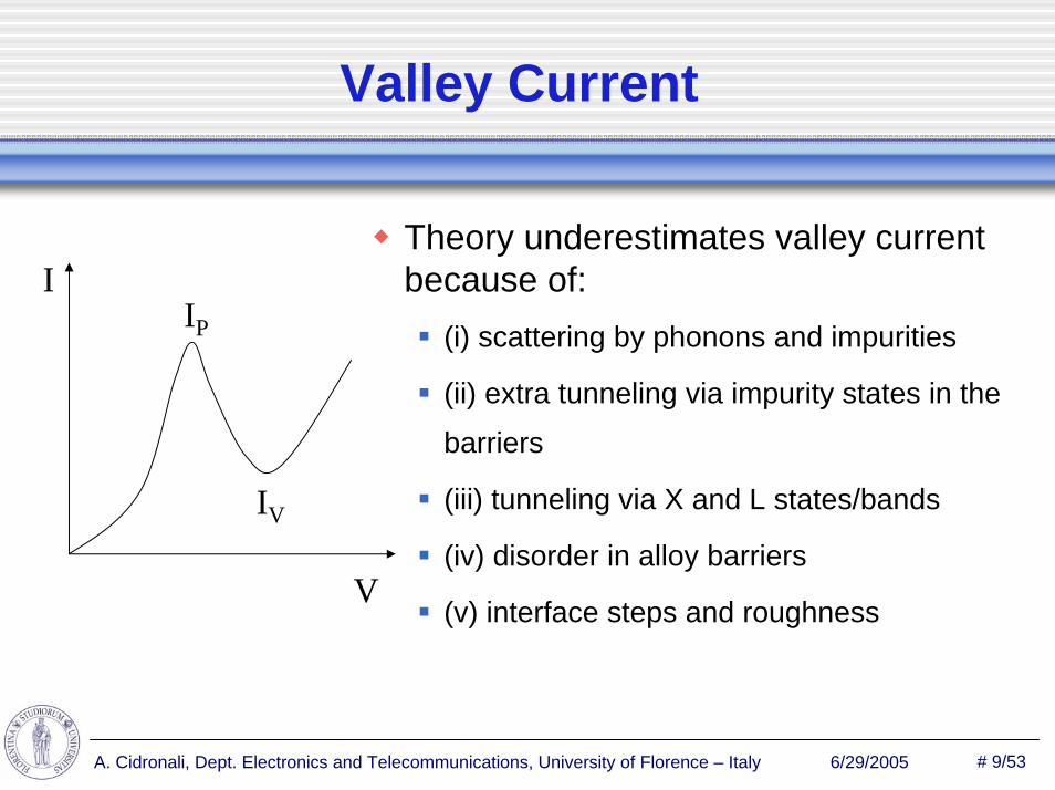
Valley Current
Theory underestimates valley current because of:
(i) scattering by phonons and impurities
(ii) extra tunneling via impurity states in the
barriers
(iii) tunneling via X and L states/bands
(iv) disorder in alloy barriers
(v) interface steps and roughness
IP
IV
V
I
# 10/53A. Cidronali, Dept. Electronics and Telecommunications, University of Florence – Italy 6/29/2005
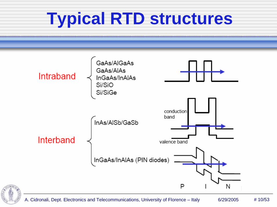
Typical RTD structures
# 11/53A. Cidronali, Dept. Electronics and Telecommunications, University of Florence – Italy 6/29/2005
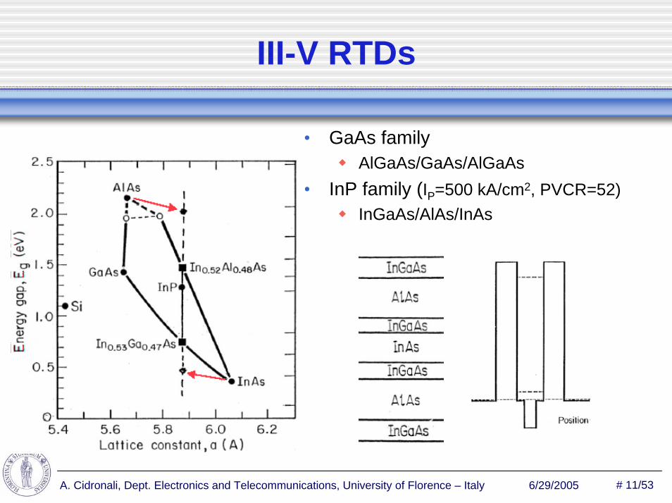
III-V RTDs
• GaAs familyAlGaAs/GaAs/AlGaAs
• InP family (IP=500 kA/cm2, PVCR=52)InGaAs/AlAs/InAs
# 12/53A. Cidronali, Dept. Electronics and Telecommunications, University of Florence – Italy 6/29/2005
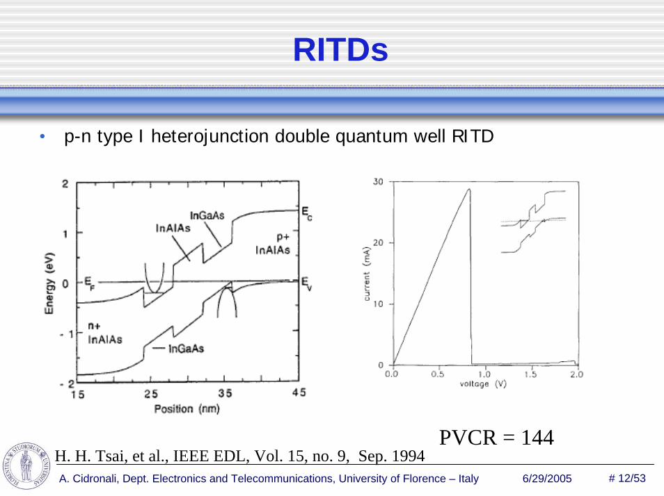
RITDs
• p-n type I heterojunction double quantum well RITD
PVCR = 144H. H. Tsai, et al., IEEE EDL, Vol. 15, no. 9, Sep. 1994
# 13/53A. Cidronali, Dept. Electronics and Telecommunications, University of Florence – Italy 6/29/2005
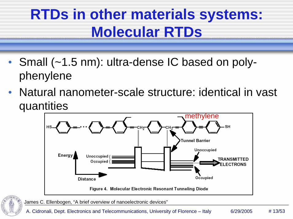
RTDs in other materials systems: Molecular RTDs
• Small (~1.5 nm): ultra-dense IC based on poly-phenylene
• Natural nanometer-scale structure: identical in vast quantities
methylene
James C. Ellenbogen, “A brief overview of nanoelectronic devices”

# 14/53A. Cidronali, Dept. Electronics and Telecommunications, University of Florence – Italy 6/29/2005
# 15/53A. Cidronali, Dept. Electronics and Telecommunications, University of Florence – Italy 6/29/2005
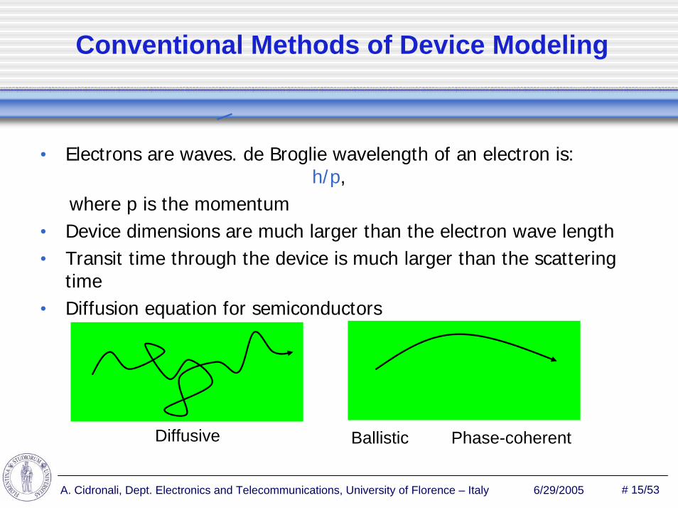
Conventional Methods of Device Modeling
• Electrons are waves. de Broglie wavelength of an electron is: h/p,
where p is the momentum• Device dimensions are much larger than the electron wave length• Transit time through the device is much larger than the scattering
time• Diffusion equation for semiconductors
Diffusive Ballistic Phase-coherent
# 16/53A. Cidronali, Dept. Electronics and Telecommunications, University of Florence – Italy 6/29/2005
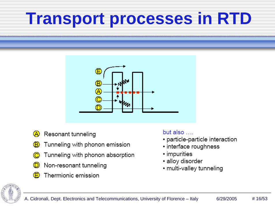
Transport processes in RTD
# 17/53A. Cidronali, Dept. Electronics and Telecommunications, University of Florence – Italy 6/29/2005
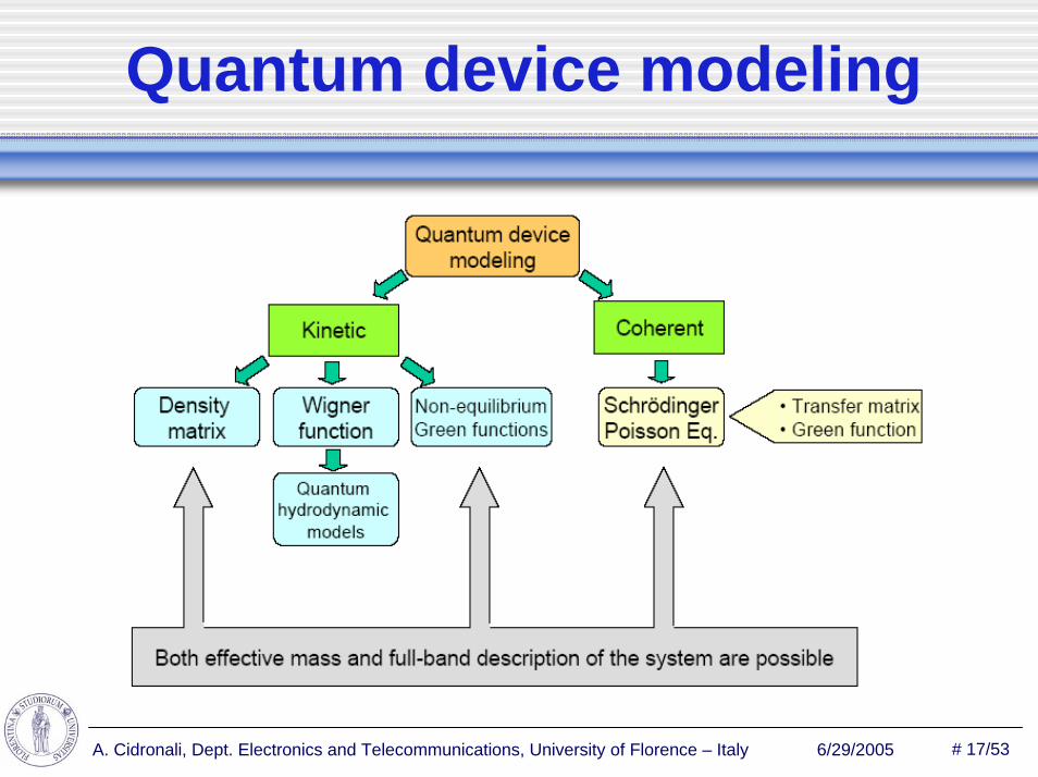
Quantum device modeling
# 18/53A. Cidronali, Dept. Electronics and Telecommunications, University of Florence – Italy 6/29/2005
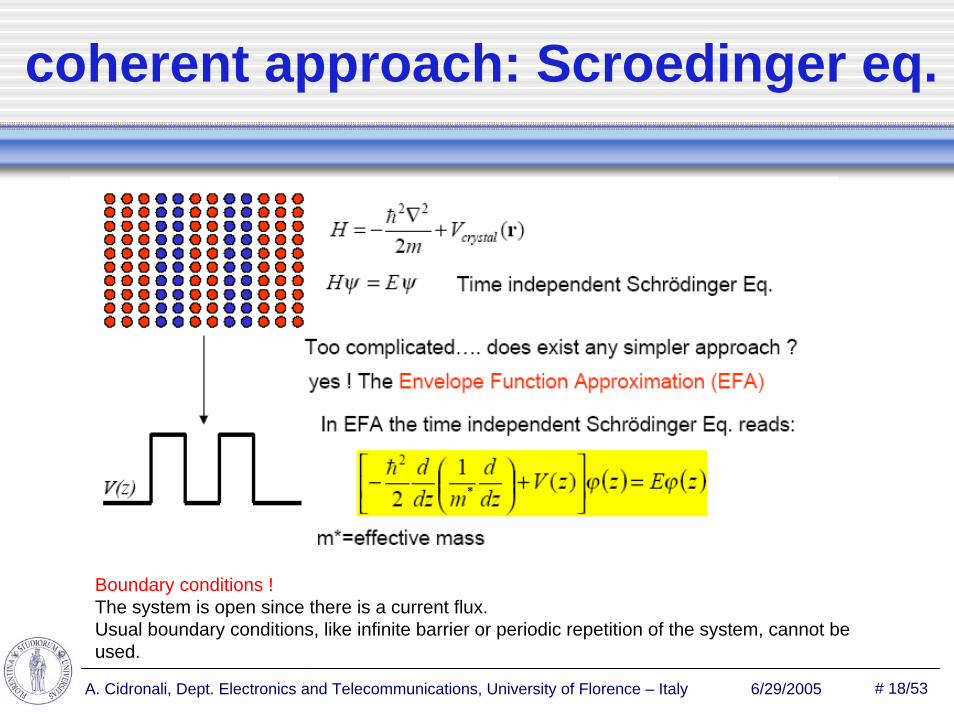
coherent approach: Scroedinger eq.
Boundary conditions !The system is open since there is a current flux.Usual boundary conditions, like infinite barrier or periodic repetition of the system, cannot be used.
# 19/53A. Cidronali, Dept. Electronics and Telecommunications, University of Florence – Italy 6/29/2005
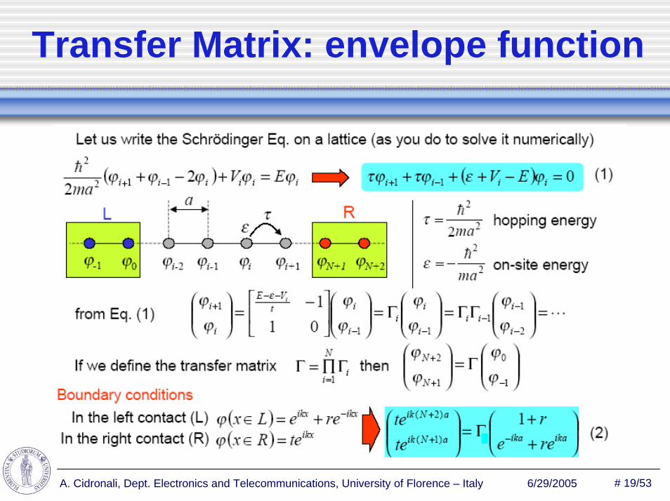
Transfer Matrix: envelope function
# 20/53A. Cidronali, Dept. Electronics and Telecommunications, University of Florence – Italy 6/29/2005
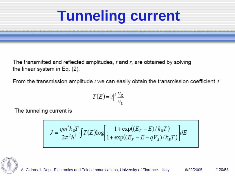
Tunneling current

# 21/53A. Cidronali, Dept. Electronics and Telecommunications, University of Florence – Italy 6/29/2005
Self-consistent calculations

# 22/53A. Cidronali, Dept. Electronics and Telecommunications, University of Florence – Italy 6/29/2005
Wigner function
( ) ( ),WJ r q k f r k dk+∞
−∞
= − ⋅∫
( ) ( ),Wn r f r k dk+∞
−∞
= ∫
( ) ˆ,i x t Htψ ψ
∂=
∂( ) ( ) ( ), , , ,r s t r t s tρ ψ ψ= ⋅
Density matrix
1.Change of basis
2.Fourier transform
# 23/53A. Cidronali, Dept. Electronics and Telecommunications, University of Florence – Italy 6/29/2005
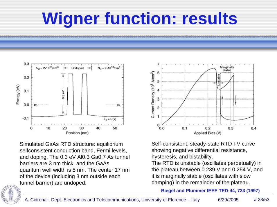
Wigner function: results
Simulated GaAs RTD structure: equilibrium selfconsistent conduction band, Fermi levels, and doping. The 0.3 eV Al0.3 Ga0.7 As tunnel barriers are 3 nm thick, and the GaAsquantum well width is 5 nm. The center 17 nm of the device (including 3 nm outside each tunnel barrier) are undoped.
Self-consistent, steady-state RTD I-V curve showing negative differential resistance, hysteresis, and bistability.The RTD is unstable (oscillates perpetually) in the plateau between 0.239 V and 0.254 V, and it is marginally stable (oscillates with slow damping) in the remainder of the plateau.
Biegel and Plummer IEEE TED-44, 733 (1997)
# 24/53A. Cidronali, Dept. Electronics and Telecommunications, University of Florence – Italy 6/29/2005
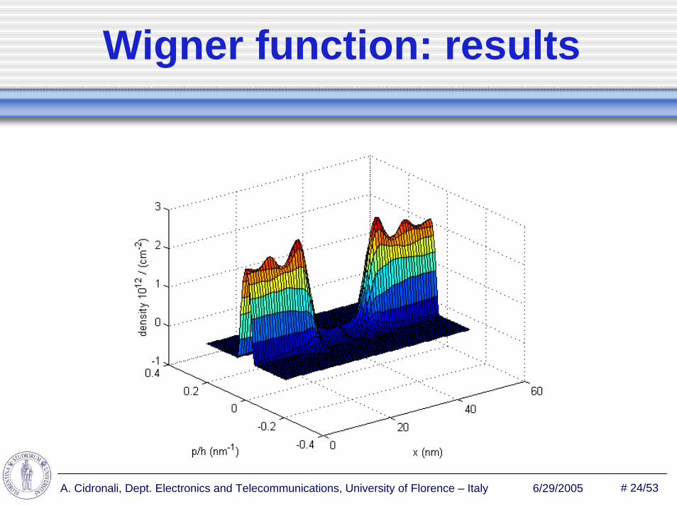
Wigner function: results
# 25/53A. Cidronali, Dept. Electronics and Telecommunications, University of Florence – Italy 6/29/2005
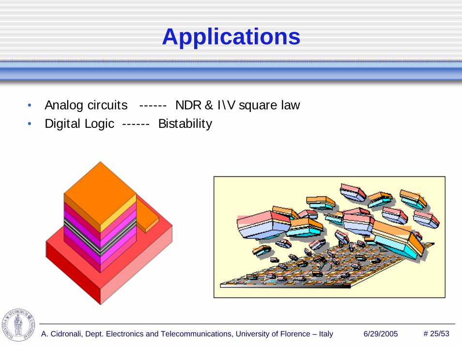
Applications
• Analog circuits ------ NDR & I\V square law• Digital Logic ------ Bistability
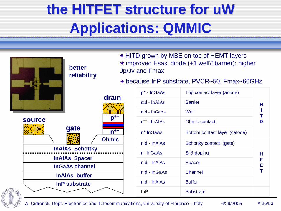
# 26/53A. Cidronali, Dept. Electronics and Telecommunications, University of Florence – Italy 6/29/2005
the HITFET structure for the HITFET structure for uWuWApplications: QMMIC
InP substrate
InGaAs channel
gatesource
InAlAs buffer
InAlAs Schottky
drain
p++
n++
Ohmic
InAlAs Spacer
HITD grown by MBE on top of HEMT layersimproved Esaki diode (+1 well\1barrier): higher
Jp/Jv and Fmax
because InP substrate, PVCR~50, Fmax~60GHz
p+ - InGaAs Top contact layer (anode)
HITD
nid - InAlAs Barrier
nid - InGaAs Well
n++ - InAlAs Ohmic contact
n+ InGaAs Bottom contact layer (catode)
nid - InAlAs Schottky contact (gate)
HFET
n- InGaAs Si δ-doping
nid - InAlAs Spacer
nid - InGaAs Channel
nid - InAlAs Buffer
InP Substrate
better reliability
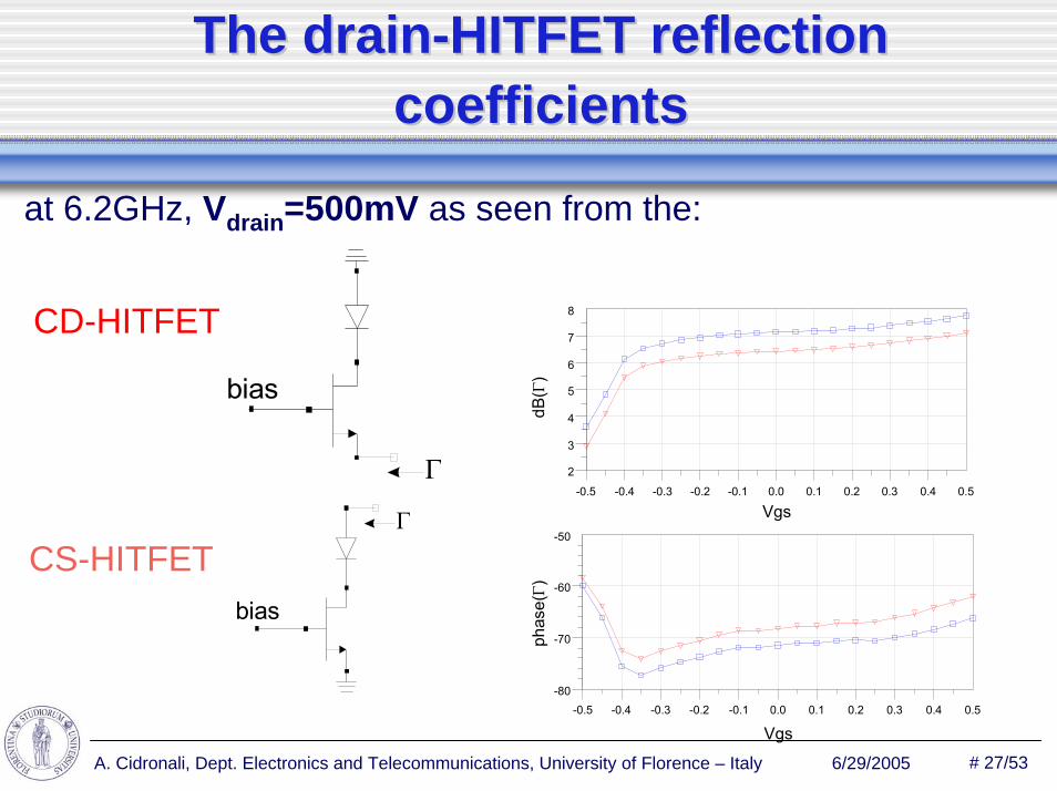
# 27/53A. Cidronali, Dept. Electronics and Telecommunications, University of Florence – Italy 6/29/2005
The drainThe drain--HITFET reflection HITFET reflection coefficientscoefficients
at 6.2GHz, Vdrain=500mV as seen from the:
bias
Γ
CD-HITFET
-0.5 -0.4 -0.3 -0.2 -0.1 0.0 0.1 0.2 0.3 0.4 0.5
2
3
4
5
6
7
8
Vgs
dB
()Γ
phas
e(
)Γ
-0.5 -0.4 -0.3 -0.2 -0.1 0.0 0.1 0.2 0.3 0.4 0.5
-80
-70
-60
-50
Vgs
bias
Γ
CS-HITFET
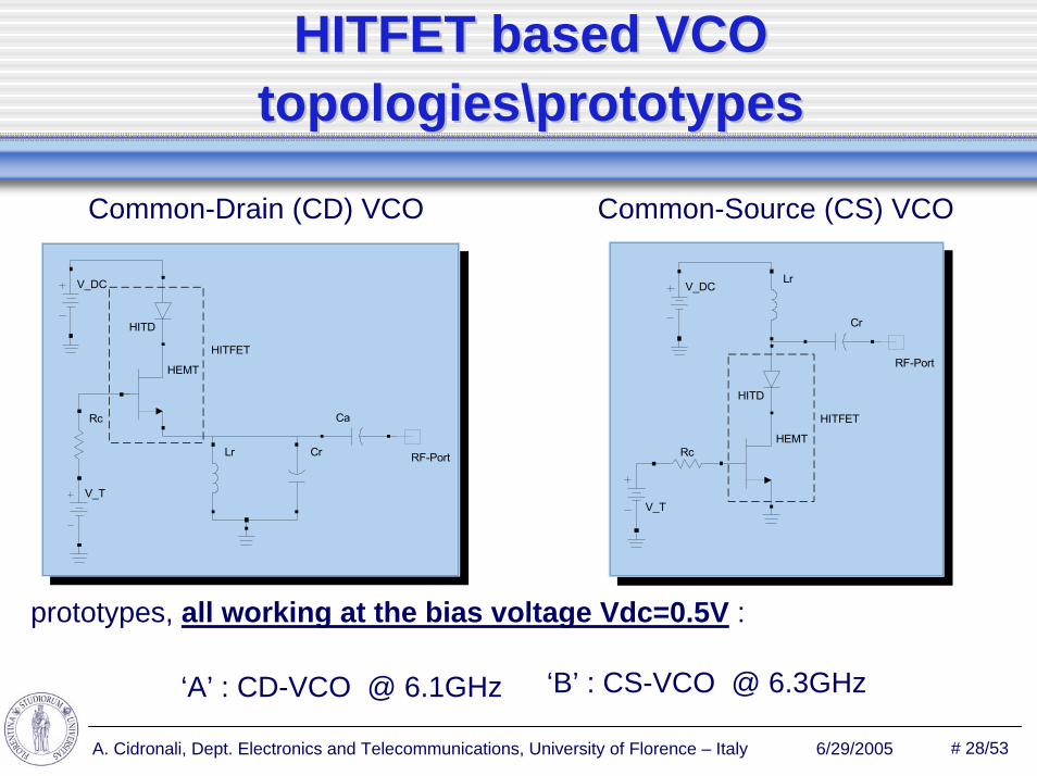
# 28/53A. Cidronali, Dept. Electronics and Telecommunications, University of Florence – Italy 6/29/2005
HITFET based VCO HITFET based VCO topologiestopologies\\prototypesprototypes
V_DC
RF-Port
HITD
Lr Cr
Ca
V_T
Rc
HEMT
HITFET
Common-Drain (CD) VCO Common-Source (CS) VCO
V_DC
RF-Port
HITD
Lr
Cr
V_T
RcHEMT
HITFET
prototypes, all working at the bias voltage Vdc=0.5V :
‘B’ : CS-VCO @ 6.3GHz‘A’ : CD-VCO @ 6.1GHz
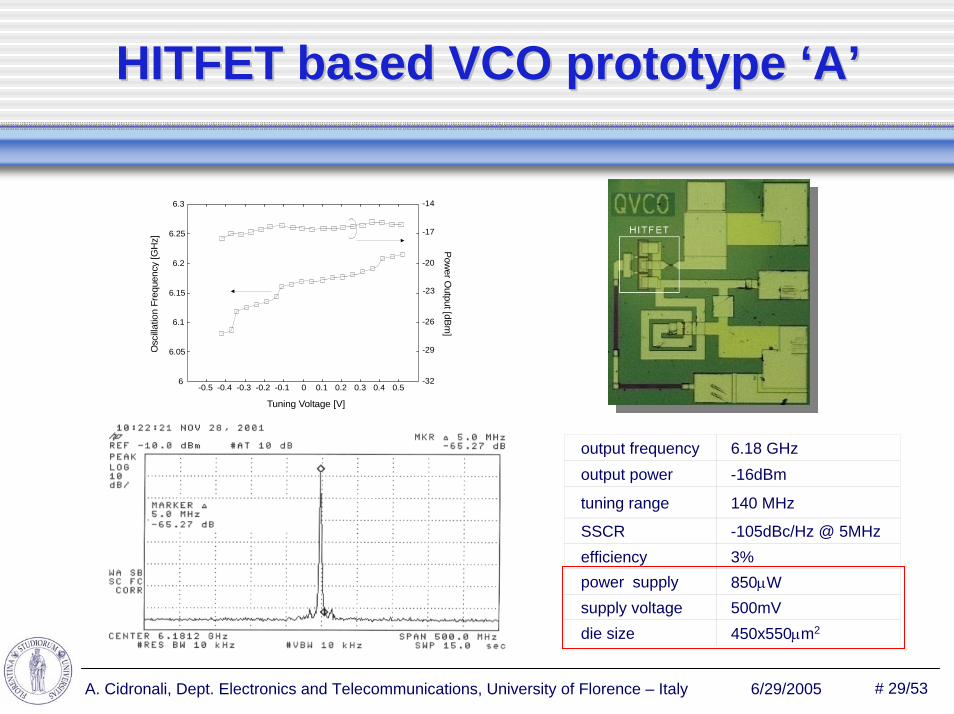
# 29/53A. Cidronali, Dept. Electronics and Telecommunications, University of Florence – Italy 6/29/2005
HITFET based VCO prototype HITFET based VCO prototype ‘‘AA’’
-32
-29
-26
Power O
utput[dBm]
-20
-23
-17
-14
-0.5 -0.4 -0.3 -0.2 -0.1 0
Tuning Voltage [V]
0.1 0.2 0.3 0.4 0.56
6.05
6.1
6.15
Osc
illatio
n Fr
eque
ncy
[GH
z]
6.2
6.25
6.3
tuning range 140 MHz
efficiency 3% SSCR -105dBc/Hz @ 5MHz
die size 450x550µm2
power supply 850µWsupply voltage 500mV
output frequency 6.18 GHzoutput power -16dBm
# 30/53A. Cidronali, Dept. Electronics and Telecommunications, University of Florence – Italy 6/29/2005
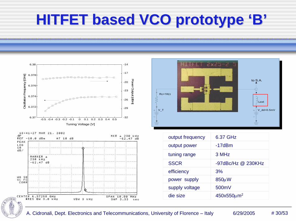
HITFET based VCO prototype HITFET based VCO prototype ‘‘BB’’
V_T
Rc=1KΩ
V_dd=0.5mV
Lext
to S.A.
6.37
6.372
6.374
6.376
6.378
6.38
-32
-29
-26
Power O
utput [dBm]
-20
-23
-17
-14
-0.5 -0.4 -0.3 -0.2 -0.1 0
Tuning Voltage [V]
0.1 0.2 0.3 0.4 0.5
Osc
illatio
n Fr
eque
ncy
[GHz]
tuning range 3 MHz
efficiency 3% SSCR -97dBc/Hz @ 230KHz
die size 450x550µm2
power supply 850µWsupply voltage 500mV
output frequency 6.37 GHz
output power -17dBm

# 31/53A. Cidronali, Dept. Electronics and Telecommunications, University of Florence – Italy 6/29/2005
figure of merit (4figure of merit (4--6.5GHz)6.5GHz)
( )
20 1n nDC
fFOM
f P SSCR f⎛ ⎞⎟⎜= ⎟⎜ ⎟⎜⎝ ⎠ ⋅
1. Arhens, MOS w/ resonator, proc. ISSC 1996
2. Kinget, 0.35um CMOS, proc. ISSC 1998
3. Shealy, GaN FET, IEEE MWCL 2001
4. Yu, InP HBT, IEEE MWCL 2001
5. Mostafa, 0.35um CMOS sub-1V, IEEE T-CS-II 2001
6. Mostafa, 0.35um CMOS, proc. IEEE CS 2001
7. Loo, BJT differential, 2000 Canadian Conf.
8. Liu, 0.35um CMOS, proc. ISSC 1998
9. Vaananen, 0.35um BiCMOS, IEEE JSSC 2001
10. Van de Ven, LC MOS, 2001 Sym. VLSI
11. Ellinger, classE GaAs VCO, IEEE T-MTT 2001
12. Deval, Synchronous CMOS VCO, IEEE RFIC Sym. 2001
13. Klepser, SiGe BiCMOS, IEEE RFIC Sym. 20014 4.5 5 5.5
freq, GHz
Si - devicesIII-V - devices
Figu
re o
f Mer
it, d
B
6 6.5125
130
135
140
145
150
[1][2]
[9]
[5] [6]
[10]
[7]
[12][13]
[4]
[3]
[8]
[11]
[this work: prot.’C’ ] [this work: prot.’B’ ]
[this work: prot.’A’ ]155
160
165
170
175
HITFET-VCOs show the lowest power supplyHITFET-VCOs show the lowest power supply
# 32/53A. Cidronali, Dept. Electronics and Telecommunications, University of Florence – Italy 6/29/2005
the QMMIC limitation
• Not all the active functions can be replaced; e.g. difficult to replace LNA, PA, Switch
• On a one-to-one basis, the individual functions in QMMIC could be more effective than conventional ones (e.g. VCOs and mixers)
• In the overall budget, however, the benefit might be marginal
# 33/53A. Cidronali, Dept. Electronics and Telecommunications, University of Florence – Italy 6/29/2005
the QMMIC as enabling technologythe QMMIC as enabling technology
How to improve the effectiveness taking advantage of How to improve the effectiveness taking advantage of the unique features of QMMIC technology?the unique features of QMMIC technology?By introducing appropriate architectures whose By introducing appropriate architectures whose application is enabled by the features of QMMIC application is enabled by the features of QMMIC technologytechnology
-- enabling technology approach enabling technology approach --
the Quantum Bi-Directional Amplifer (QBDA) for
Tagging Applications
# 34/53A. Cidronali, Dept. Electronics and Telecommunications, University of Florence – Italy 6/29/2005
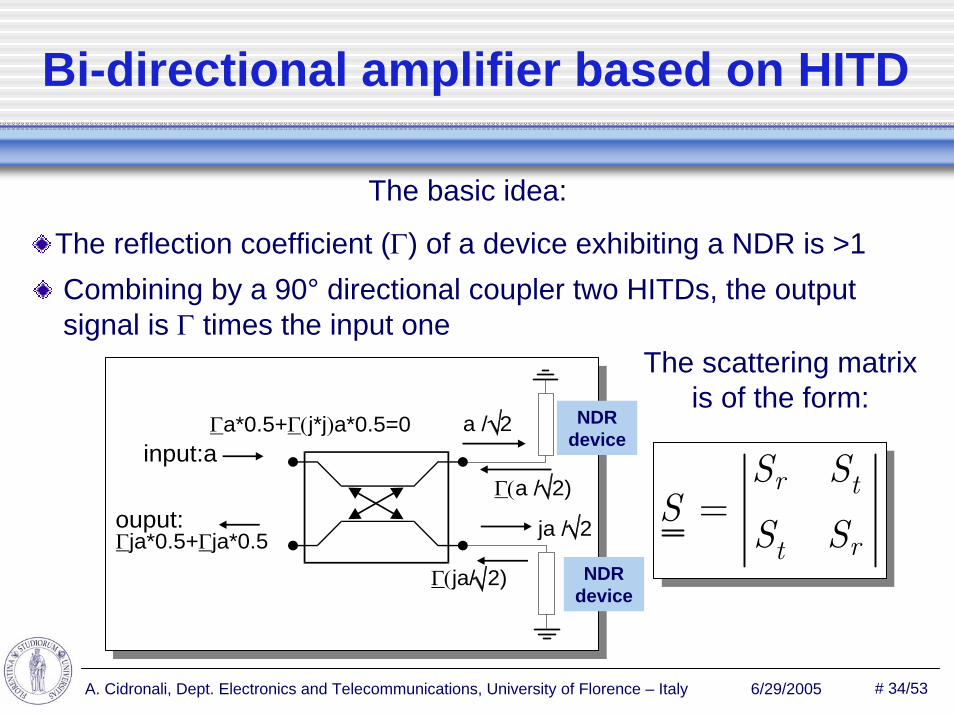
Bi-directional amplifier based on HITD
The basic idea:
The reflection coefficient (Γ) of a device exhibiting a NDR is >1
r t
rt
S SS
S S=
The scattering matrix is of the form:
a / 2
ja / 2Γ Γja*0.5ja*0.5+
Γa*0.5+Γ( )j*j a*0.5=0
Γ(ja/ 2)
Γ(a / 2)input:a
ouput:
NDR device
NDR device
Combining by a 90° directional coupler two HITDs, the output signal is Γ times the input one
# 35/53A. Cidronali, Dept. Electronics and Telecommunications, University of Florence – Italy 6/29/2005
QBDA prototype
3.0 3.5 4.0 4.5 5.0 5.5 6.0 6.5 7.0 7.5 8.0 8.5 9.0
-15
-10
-5
0
5
10
freq, GHz
dB
(S(2
,1))
dB
(S(1
,2))
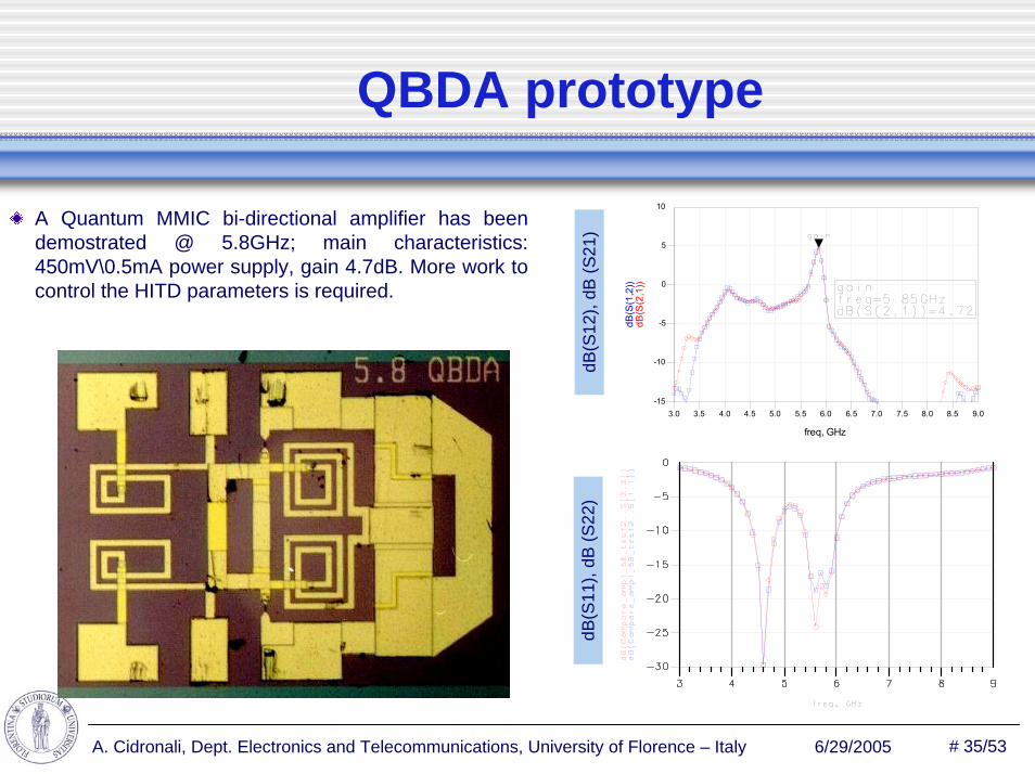
A Quantum MMIC bi-directional amplifier has been demostrated @ 5.8GHz; main characteristics: 450mV\0.5mA power supply, gain 4.7dB. More work to control the HITD parameters is required.
dB(S
11),
dB (S
22)
dB(S
12),
dB (S
21)
# 36/53A. Cidronali, Dept. Electronics and Telecommunications, University of Florence – Italy 6/29/2005
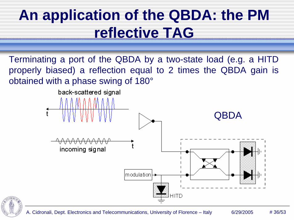
An application of the QBDA: the PM reflective TAG
Terminating a port of the QBDA by a two-state load (e.g. a HITD properly biased) a reflection equal to 2 times the QBDA gain is obtained with a phase swing of 180°
QBDA
# 37/53A. Cidronali, Dept. Electronics and Telecommunications, University of Florence – Italy 6/29/2005
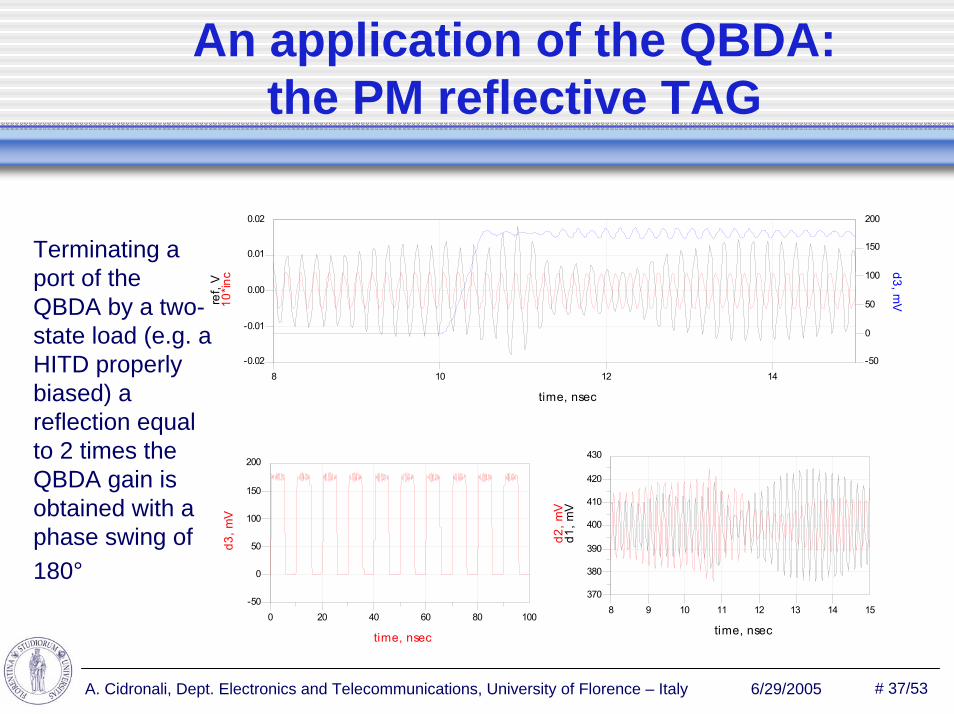
An application of the QBDA: the PM reflective TAG
Terminating a port of the QBDA by a two-state load (e.g. a HITD properly biased) a reflection equal to 2 times the QBDA gain is obtained with a phase swing of 180°
8 10 12 14
-0.02
-0.01
0.00
0.01
0.02
-50
0
50
100
150
200
time, nsec
10
*in
cre
f, V
d3
, mV
8 9 10 11 12 13 14 15
370
380
390
400
410
420
430
time, nsec
d1
, m
Vd
2,
mV
0 20 40 60 80 100
-50
0
50
100
150
200
time, nsec
d3
, m
V
# 38/53A. Cidronali, Dept. Electronics and Telecommunications, University of Florence – Italy 6/29/2005
QMMIC Summary
Highlights:– TDs may be considered as an optimizing technology for
extremely low power (<500mV) RF electronics, (e.g. VCO). – new circuit functionalities are enabled by Tunnel Devices.– at system and circuit levels, TDs introduce new degree of
freedom, (e.g. BDA).
Next steps:– Tight control of series resistance and parasitics.– Device engineering at quantum mechanic level.– Application to millimeter-wave transceiver
# 39/53A. Cidronali, Dept. Electronics and Telecommunications, University of Florence – Italy 6/29/2005
Applications — Digital Logic
• Logic circuits ------ Bistability
• Integration with transistors (HEMT, HBT, CMOS) is a requirement for a complete IC technology based on RTDs
Transitors: Input/output isolation, controllable gain
RTDs: increased functionality, enhanced circuit speed, reduced power consumption
• It’s all about Load lines!
# 40/53A. Cidronali, Dept. Electronics and Telecommunications, University of Florence – Italy 6/29/2005
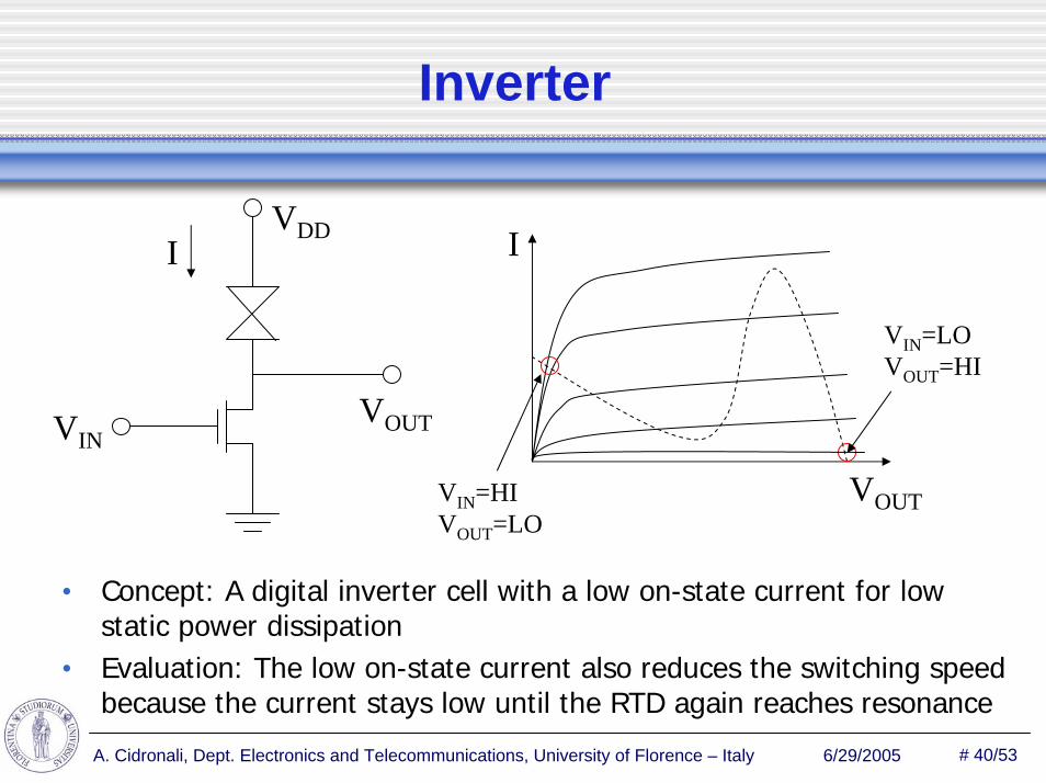
Inverter
VDD II
• Concept: A digital inverter cell with a low on-state current for low static power dissipation
• Evaluation: The low on-state current also reduces the switching speed because the current stays low until the RTD again reaches resonance
VINVOUT
VOUTVIN=HIVOUT=LO
VIN=LOVOUT=HI
# 41/53A. Cidronali, Dept. Electronics and Telecommunications, University of Florence – Italy 6/29/2005
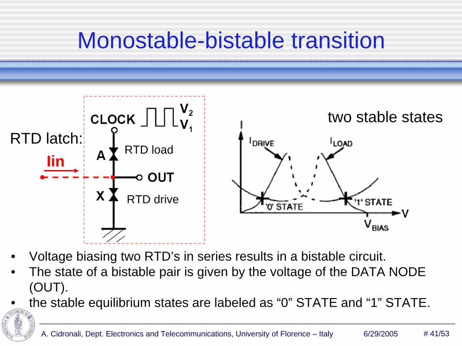
Monostable-bistable transition
RTD load
RTD drive
• Voltage biasing two RTD’s in series results in a bistable circuit. • The state of a bistable pair is given by the voltage of the DATA NODE
(OUT). • the stable equilibrium states are labeled as “0” STATE and “1” STATE.
RTD latch:two stable states
Iin
# 42/53A. Cidronali, Dept. Electronics and Telecommunications, University of Florence – Italy 6/29/2005
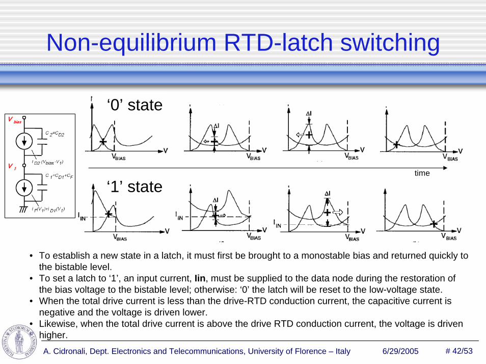
Non-equilibrium RTD-latch switching
‘0’ state
‘1’ statetime
• To establish a new state in a latch, it must first be brought to a monostable bias and returned quickly to the bistable level.
• To set a latch to ‘1’, an input current, Iin, must be supplied to the data node during the restoration of the bias voltage to the bistable level; otherwise: ‘0’ the latch will be reset to the low-voltage state.
• When the total drive current is less than the drive-RTD conduction current, the capacitive current is negative and the voltage is driven lower.
• Likewise, when the total drive current is above the drive RTD conduction current, the voltage is driven higher.
# 43/53A. Cidronali, Dept. Electronics and Telecommunications, University of Florence – Italy 6/29/2005
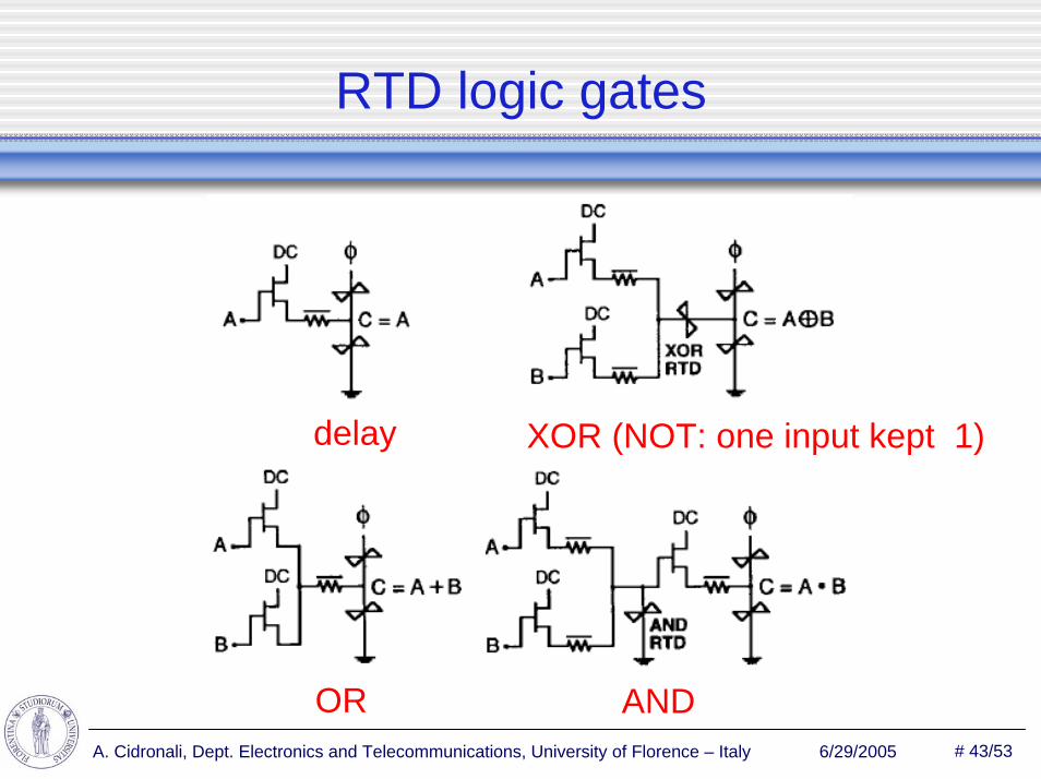
RTD logic gates
delay XOR (NOT: one input kept 1)
OR AND
# 44/53A. Cidronali, Dept. Electronics and Telecommunications, University of Florence – Italy 6/29/2005
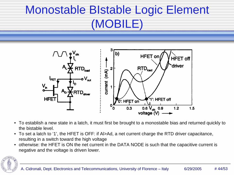
Monostable BIstable Logic Element (MOBILE)
• To establish a new state in a latch, it must first be brought to a monostable bias and returned quickly to the bistable level.
• To set a latch to ‘1’, the HFET is OFF: if Al>Ad, a net current charge the RTD driver capacitance, resulting in a switch toward the high voltage
• otherwise: the HFET is ON the net current in the DATA NODE is such that the capacitive current is negative and the voltage is driven lower.
# 45/53A. Cidronali, Dept. Electronics and Telecommunications, University of Florence – Italy 6/29/2005
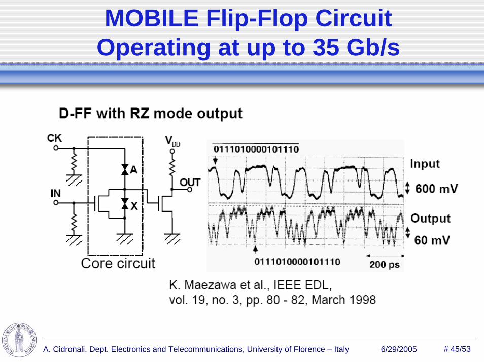
MOBILE Flip-Flop CircuitOperating at up to 35 Gb/s
# 46/53A. Cidronali, Dept. Electronics and Telecommunications, University of Florence – Italy 6/29/2005
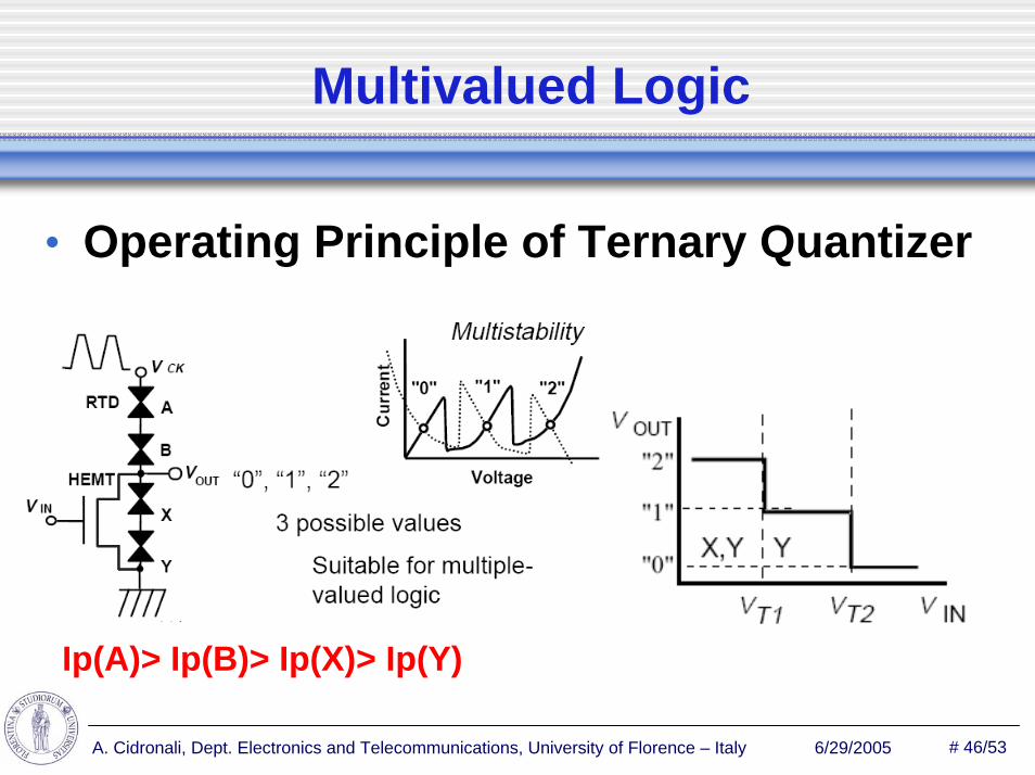
Multivalued Logic
• Operating Principle of Ternary Quantizer
Ip(A)> Ip(B)> Ip(X)> Ip(Y)
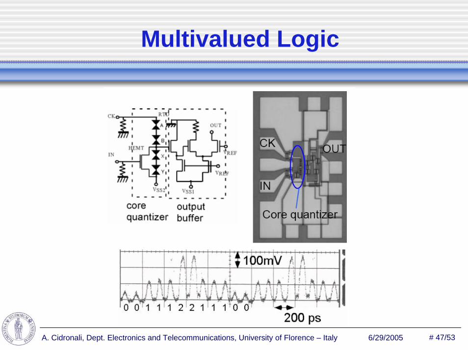
# 47/53A. Cidronali, Dept. Electronics and Telecommunications, University of Florence – Italy 6/29/2005
Multivalued Logic
# 48/53A. Cidronali, Dept. Electronics and Telecommunications, University of Florence – Italy 6/29/2005
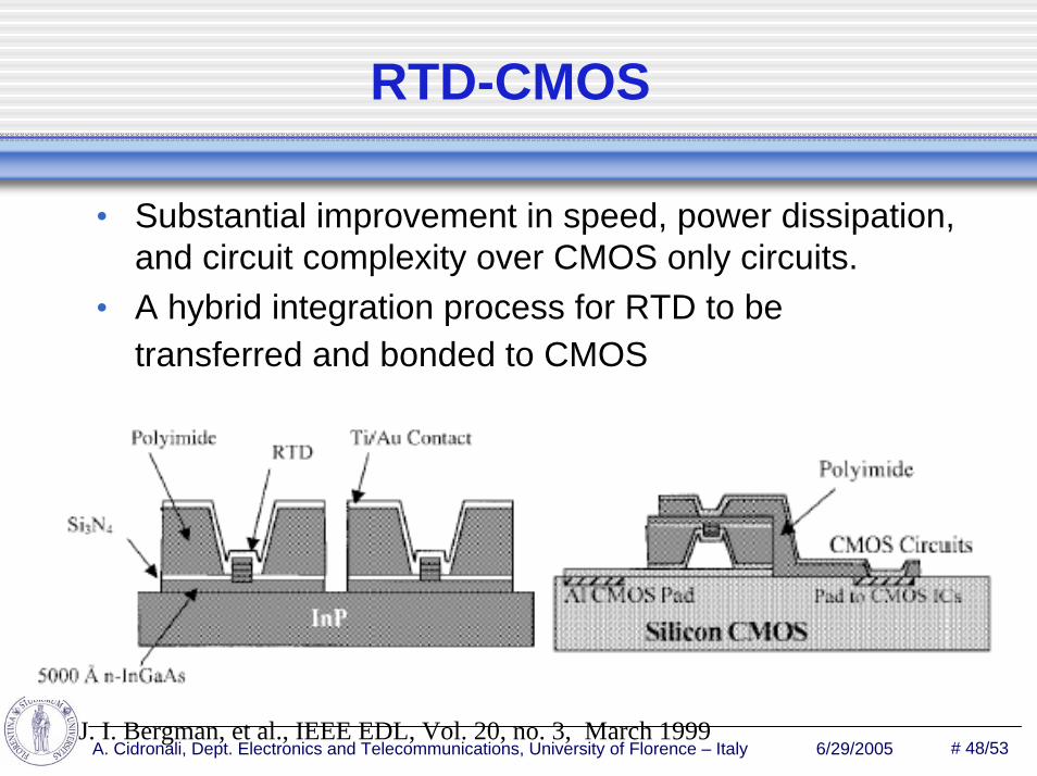
RTD-CMOS
• Substantial improvement in speed, power dissipation, and circuit complexity over CMOS only circuits.
• A hybrid integration process for RTD to be transferred and bonded to CMOS
J. I. Bergman, et al., IEEE EDL, Vol. 20, no. 3, March 1999
# 49/53A. Cidronali, Dept. Electronics and Telecommunications, University of Florence – Italy 6/29/2005
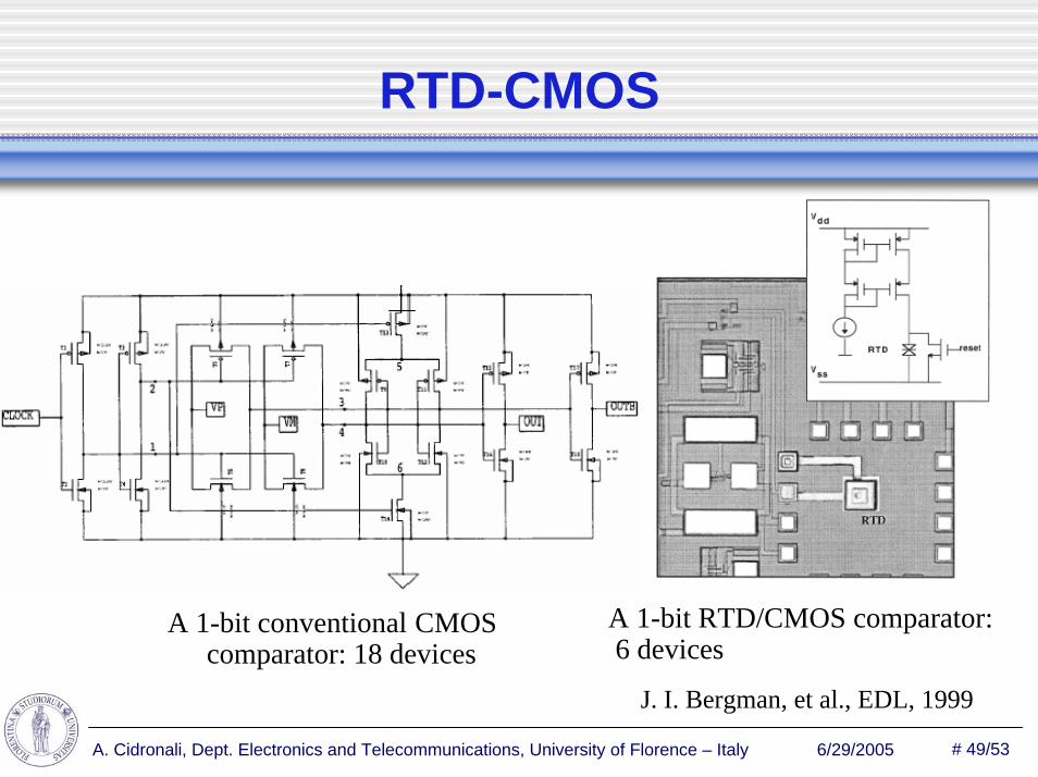
RTD-CMOS
A 1-bit conventional CMOS comparator: 18 devices
A 1-bit RTD/CMOS comparator:6 devices
J. I. Bergman, et al., EDL, 1999
# 50/53A. Cidronali, Dept. Electronics and Telecommunications, University of Florence – Italy 6/29/2005
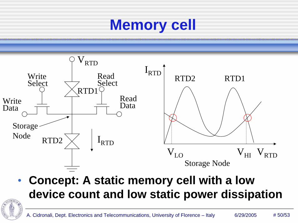
Memory cell
VRTDIRTD
ReadData
WriteSelect
ReadSelect RTD2 RTD1
• Concept: A static memory cell with a low device count and low static power dissipation
WriteData
IRTD
RTD1
RTD2VRTD
StorageNode
VLO VHIStorage Node
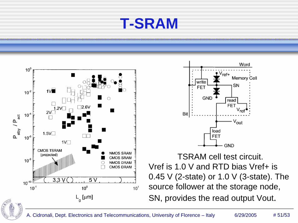
# 51/53A. Cidronali, Dept. Electronics and Telecommunications, University of Florence – Italy 6/29/2005
T-SRAM
TSRAM cell test circuit. Vref is 1.0 V and RTD bias Vref+ is 0.45 V (2-state) or 1.0 V (3-state). The source follower at the storage node, SN, provides the read output Vout.
# 52/53A. Cidronali, Dept. Electronics and Telecommunications, University of Florence – Italy 6/29/2005
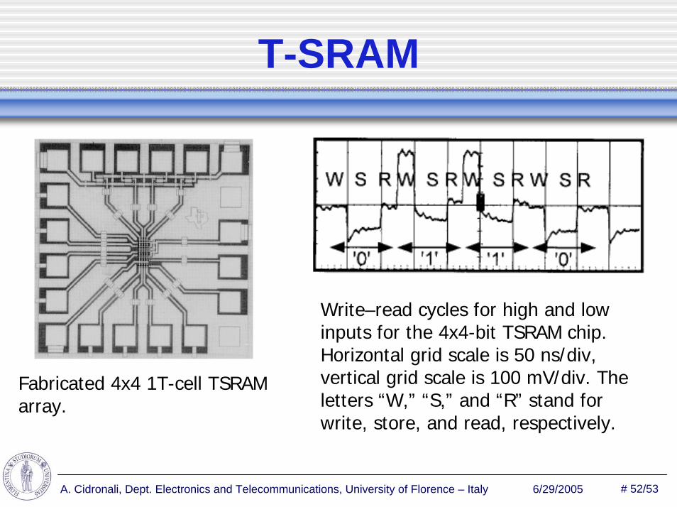
T-SRAM
Write–read cycles for high and low inputs for the 4x4-bit TSRAM chip. Horizontal grid scale is 50 ns/div, vertical grid scale is 100 mV/div. The letters “W,” “S,” and “R” stand forwrite, store, and read, respectively.
Fabricated 4x4 1T-cell TSRAM array.
# 53/53A. Cidronali, Dept. Electronics and Telecommunications, University of Florence – Italy 6/29/2005
Promising Future