
Resistive Touch Sensors With a practical Modal of " Touch Hand Shake ".
Upload
trinhtuongCategory
view
221download
1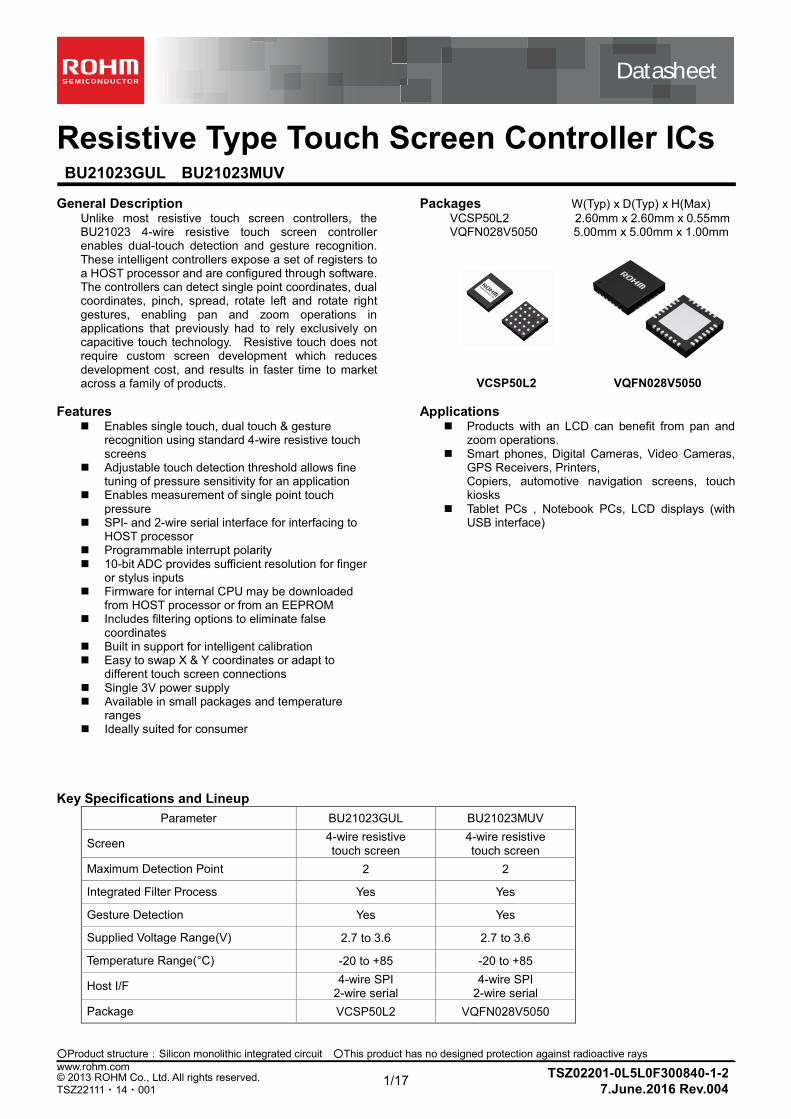
○Product structure:Silicon monolithic integrated circuit ○This product has no designed protection against radioactive rays
.
1/17 TSZ02201-0L5L0F300840-1-2 © 2013 ROHM Co., Ltd. All rights reserved.
7.June.2016 Rev.004 TSZ22111・14・001
www.rohm.com
Resistive Type Touch Screen Controller ICs BU21023GUL BU21023MUV
General Description Unlike most resistive touch screen controllers, the BU21023 4-wire resistive touch screen controller enables dual-touch detection and gesture recognition. These intelligent controllers expose a set of registers to a HOST processor and are configured through software. The controllers can detect single point coordinates, dual coordinates, pinch, spread, rotate left and rotate right gestures, enabling pan and zoom operations in applications that previously had to rely exclusively on capacitive touch technology. Resistive touch does not require custom screen development which reduces development cost, and results in faster time to market across a family of products.
Features Enables single touch, dual touch & gesture
recognition using standard 4-wire resistive touch screens
Adjustable touch detection threshold allows fine tuning of pressure sensitivity for an application
Enables measurement of single point touch pressure
SPI- and 2-wire serial interface for interfacing to HOST processor
Programmable interrupt polarity 10-bit ADC provides sufficient resolution for finger
or stylus inputs Firmware for internal CPU may be downloaded
from HOST processor or from an EEPROM Includes filtering options to eliminate false
coordinates Built in support for intelligent calibration Easy to swap X & Y coordinates or adapt to
different touch screen connections Single 3V power supply Available in small packages and temperature
ranges Ideally suited for consumer
Packages W(Typ) x D(Typ) x H(Max)
VCSP50L2 2.60mm x 2.60mm x 0.55mm VQFN028V5050 5.00mm x 5.00mm x 1.00mm
VCSP50L2 VQFN028V5050
Applications Products with an LCD can benefit from pan and
zoom operations. Smart phones, Digital Cameras, Video Cameras,
GPS Receivers, Printers, Copiers, automotive navigation screens, touch kiosks
Tablet PCs , Notebook PCs, LCD displays (with USB interface)
Key Specifications and Lineup
Parameter BU21023GUL BU21023MUV
Screen 4-wire resistive touch screen
4-wire resistive touch screen
Maximum Detection Point 2 2
Integrated Filter Process Yes Yes
Gesture Detection Yes Yes
Supplied Voltage Range(V) 2.7 to 3.6 2.7 to 3.6
Temperature Range(°C) -20 to +85 -20 to +85
Host I/F 4-wire SPI
2-wire serial 4-wire SPI
2-wire serial
Package VCSP50L2 VQFN028V5050
Datasheet
BU21023GUL BU21023MUV BU21024FV-M
2/17
TSZ02201-0L5L0F300840-1-2 © 2013 ROHM Co., Ltd. All rights reserved. 7.June.2016 Rev.004
www.rohm.com
TSZ22111・15・001
Pin Configuration and Pin Description
【BU21023GUL】
TOP VIEW (BALL SIDE DOWN) BOTTOM VIEW (BALL SIDE UP)
1 2 3 4 5
A
B
C
D
E
T4 PVDD DVDD VDD VSS
XP AVDD DVDD_EXT CLK_EXT
XN YP RSTB T1 T2
YN SEL_CSB SO T3 IFSEL
ECL EDA SCL_SCK SDA_SI INT
1 2 3 4 5
E
D
C
B
A
T4 PVDD DVDD VDD VSS
XP AVDD DVDD_EXT CLK_EXT
XN YP RSTB T1 T2
YN SEL_CSB SO T3 IFSEL
ECL EDA SCL_SCK SDA_SI INT
No. Pin Name I/O Function Figure
D1 YN I/O Screen interface E
C1 XN I/O Screen interface E
C2 YP I/O Screen interface E
B1 XP I/O Screen interface E
A1 T4 I/O Test pin E
A2 PVDD O Regulator output (for supply screen voltage) -
B3 AVDD O Regulator output (for supply analog block) -
A3 DVDD I/O Regulator output (for supply digital block) or supply digital voltage -
B4 DVDD_EXT I Digital voltage enable (H=Hi-z , L=DVDD Enable) E
A4 VDD - Supply voltage -
A5 VSS - Ground -
C3 RSTB I H/W reset E
B5 CLK_EXT I Supply external clock for debug A
C4 T1 I Test pin A
C5 T2 I Test pin A
D4 T3 I Test pin A
D5 IFSEL I Interface select pin (L=SPI, H=2-wire serial) A
D3 SO O SPI Serial data output 2-wire - F
E5 INT O Interrupt output C
D2 SEL_CSB I SPI Chip select 2-wire Slave address select C
E4 SDA_SI I/O SPI Serial data input 2-wire Serial data in-out C
E3 SCL_SCK I SPI Serial clock input 2-wire Serial clock input C
E2 EDA I/O EEPROM SDA C
E1 ECL O EEPROM SCL C
1. Please use 1.0µF capacitors between AVDD and DVDD to GND, and leave PVDD terminal open.
2. If DVDD_EXT=”H“, the DVDD pin can be connected to an external 1.8V power source.
3. Please pull up the ECL, EDA, and INT pins using 10k ohm resistors as shown in the application diagram at the end of this document.
ECL and EDA pins may be directly connected to GND if an external EEPROM is not being used. Please connect a 0.1µF capacitor between T4 and GND.
T1, T2 & T3 pins should be connected to GND.
4. When using the 2 wire serial interface, please pull up the SCL_SCK, SDA_SI pins via 10k ohms and leave SO unconnected.
5. Please note that the values of resistors and capacitors mentioned here are only recommended values.
6. RSTB should be held low until supply voltage VDD has ramped up and has reached a stable level.
7. The polarity of INT pin is programmable via register 0x30.
8. Connect CLK_EXT to GND for normal use.
9. INT terminal is used as input pin in test mode.
BU21023GUL BU21023MUV BU21024FV-M
3/17
TSZ02201-0L5L0F300840-1-2 © 2013 ROHM Co., Ltd. All rights reserved. 7.June.2016 Rev.004
www.rohm.com
TSZ22111・15・001
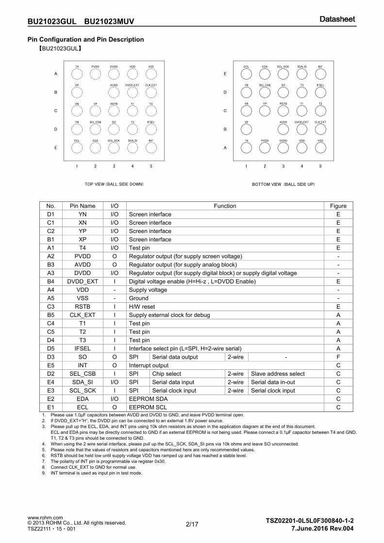
Pin Configuration and Pin Description - continued
【BU21023MUV】
No.
Pin name I/O Function Figure
1 NC - - -
2 NC - - -
3 NC - - -
4 YN I/O Screen interface E
5 XN I/O Screen interface E
6 YP I/O Screen interface E
7 XP I/O Screen interface E
8 T4 I/O Test pin E
9 PVDD O Regulator output (for supply screen voltage) -
10 AVDD O Regulator output (for supply analog block) -
11 DVDD I/O Regulator output (for supply digital block) or supply digital voltage -
12 DVDD_EXT I Digital voltage enable (H=Hi-Z , L=DVDD enable) E
13 VDD - Supply voltage -
14 VSS - Ground -
15 RSTB I H/W reset E
16 CLK_EXT I Supply external clock for debug A
17 T1 I Test pin A
18 T2 I Test pin A
19 T3 I Test pin A
20 IFSEL I Interface select pin (L=SPI, H=2-wire serial) A
21 SO O SPI Serial data output 2-wire - F
22 INT O Interrupt output C
23 SEL_CSB I SPI Chip select 2-wire Slave address select C
24 SDA_SI I/O SPI Serial data input 2-wire Serial data in-out C
25 SCL_SCK I SPI Serial clock input 2-wire Serial clock input C
26 EDA I/O EEPROM SDA C
27 ECL O EEPROM SCL C
28 NC - - -
1. Please use 1.0µF capacitors between AVDD and DVDD to GND, and leave PVDD terminal open.
2. If DVDD_EXT=”H “, the DVDD pin can be connected to an external 1.8V power source.
3. Please pull up the ECL, EDA, and INT pins using 10k ohm resistors as shown in the application diagram at the end of this document.
ECL and EDA pins may be directly connected to GND if an external EEPROM is not being used. Please connect a 0.1µF capacitor between
T4 and GND. T1, T2 & T3 pins should be connected to GND.
4. When using the 2 wire serial interface, please pull up the SCL_SCK, SDA_SI pins via 10k ohms and leave SO unconnected.
5. Please note that the values of resistors and capacitors mentioned here are only recommended values.
6. RSTB should be held low until supply voltage VDD has ramped up and has reached a stable level.
7. The polarity of INT pin is programmable via register 0x30.
8. Connect CLK_EXT to GND for normal use.
9. INT terminal is used as input pin in test mode.
10. Unconnected NC terminals.
11. Please connect thermal PAD (Exposed PAD) to GND.
22INT
23
24
25
26
27
28
SEL_CSB
SDA_SI
SCL_SCK
EDA
ECL
NC
1N
C
2N
C
3N
C
4YN
5XN
6YP
7XP
14 VSS
13
12
11
10
9
8
VDD
DVDD_EXT
DVDD
AVDD
PVDD
T4
21SO
20IF
SEL
19T3
18T2
17T1
16C
LK_E
XT
15R
STB
TOP VIEW (LEAD SIDE DOWN)
28
INT
27
26
25
24
23
22
SEL_CSB
SDA_SI
SCL_SCK
EDA
ECL
NC
21N
C
20N
C
19N
C
18YN
17XN
16YP
15XP
8
VSS
9
10
11
12
13
14
VDD
DVDD_EXT
DVDD
AVDD
PVDD
T4
1SO
2IF
SEL
3T3
4T2
5T1
6C
LK_E
XT
7R
STB
BOTTOM VIEW (LEAD SIDE UP)
BU21023GUL BU21023MUV BU21024FV-M
4/17
TSZ02201-0L5L0F300840-1-2 © 2013 ROHM Co., Ltd. All rights reserved. 7.June.2016 Rev.004
www.rohm.com
TSZ22111・15・001
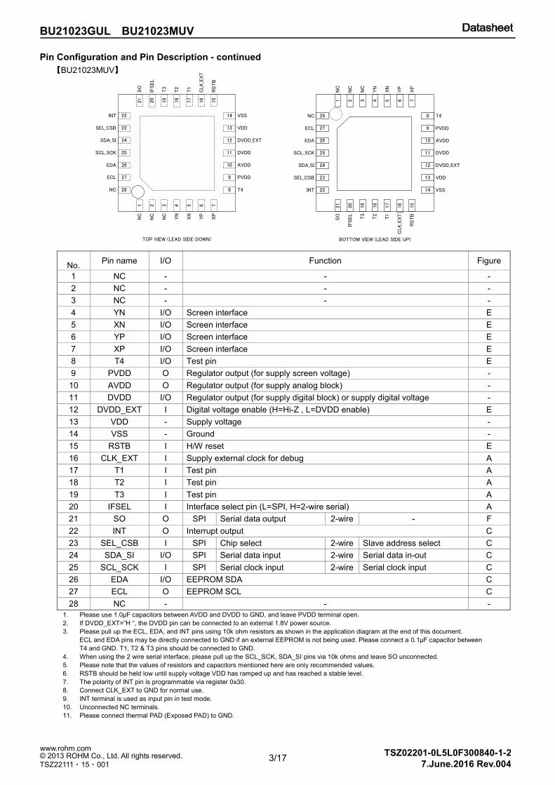
I/O equivalence circuit
PAD
PAD
PAD
PAD
PAD
CIN
PAD
Figure BU21023GUL / BU21023MUV I/O Equivalent Circuit
Figure A Figure B
Figure C Figure D
Figure E Figure F
BU21023GUL BU21023MUV BU21024FV-M
5/17
TSZ02201-0L5L0F300840-1-2 © 2013 ROHM Co., Ltd. All rights reserved. 7.June.2016 Rev.004
www.rohm.com
TSZ22111・15・001
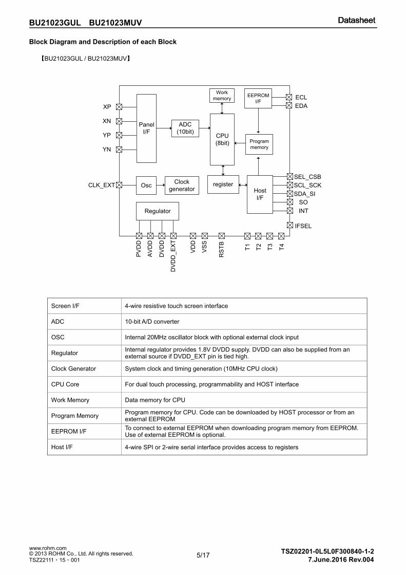
Block Diagram and Description of each Block
【BU21023GUL / BU21023MUV】
Panel
I/F
Regulator
PV
DD
AV
DD
DV
DD
DV
DD
_E
XT
VD
D
VS
S
RS
TB
Osc
ADC
(10bit)CPU
(8bit)
Work
memory
Program
memory
EEPROM
I/F
Host
I/F
registerClock
generator
T1
T2
T3
T4
CLK_EXT
XP
ECL
EDA
SEL_CSB
SCL_SCK
SDA_SI
SO
INT
YP
XN
YN
IFSEL
Screen I/F 4-wire resistive touch screen interface
ADC 10-bit A/D converter
OSC Internal 20MHz oscillator block with optional external clock input
Regulator Internal regulator provides 1.8V DVDD supply. DVDD can also be supplied from an external source if DVDD_EXT pin is tied high.
Clock Generator System clock and timing generation (10MHz CPU clock)
CPU Core For dual touch processing, programmability and HOST interface
Work Memory Data memory for CPU
Program Memory Program memory for CPU. Code can be downloaded by HOST processor or from an external EEPROM
EEPROM I/F To connect to external EEPROM when downloading program memory from EEPROM. Use of external EEPROM is optional.
Host I/F 4-wire SPI or 2-wire serial interface provides access to registers
BU21023GUL BU21023MUV BU21024FV-M
6/17
TSZ02201-0L5L0F300840-1-2 © 2013 ROHM Co., Ltd. All rights reserved. 7.June.2016 Rev.004
www.rohm.com
TSZ22111・15・001
Absolute Maximum Ratings
Parameter Symbol Rating Unit Conditions
Power Supply Voltage VDD -0.3 to +4.5 V
Input Voltage VIN -0.3 to VDD+0.3 V
Power Dissipation
BU21023GUL
Pd
0.83 (Note 1)
W
BU21023MUV 0.70 (Note 2)
W
Storage Temperature Range Tstg -50 to +125 °C
(Note1) Derate by 8.30 mW /°C centigrade when ambient temperature exceeds 25°C. Measured using PCB measuring 50mm x58mm.
(Note 2) Derate by 7.04mW /°C centigrade when ambient temperature exceeds 25°C. Measured using PCB(1 layer) measuring 74.2x74.2x1.6t mm Caution: Operating the IC over the absolute maximum ratings may damage the IC. The damage can either be a short circuit between pins or an open circuit between pins and the internal circuitry. Therefore, it is important to consider circuit protection measures, such as adding a fuse, in case the IC is operated over
the absolute maximum ratings.
Recommended Operating Conditions
Parameter Symbol Rating
Unit Conditions Min Typ Max
Power Supply Voltage VDD 2.70 3.00 3.60 V
Digital Core Power Supply DVDD 1.62 1.80 1.98 V DVDD_EXT=H
Operating Temperature Range Topr -20 +25 +85 °C
Note: The BU21023 controllers can be operated with a single 3V VDD supply.
It is also possible to supply 1.8V DVDD from an external source if the DVDD_EXT pin is connected to logic high.
Electrical Characteristics (Ta=25°C, VDD=3.00V)
Parameter Symbol Limit
Unit Conditions Min Typ Max
Low-Level Input Voltage VIL -0.5 - 0.2xVDD V
High-Level Input Voltage VIH 0.8xVDD - VDD+0.5 V
Low-Level Output Voltage VOL - - 0.4 V
High-Level Output Voltage VOH VDD-0.4 - - V
Standby Current IST - - 1 µA RSTB=L
Sleep Current1 ICC1 - 60 100 µA DVDD_EXT =L
Sleep Current2 ICC2 - 10 20 µA DVDD_EXT =H
Operating Current IDD - 4 6 mA No Load
Oscillation Frequency Freq 18 20 22 MHz
Resolution Ad 1024x1024 Bit
Differential Non-Linearity Error DNL -3.0 - +3.0 LSB
Integral Non-Linearity Error INL -3.0 - +3.0 LSB
BU21023GUL BU21023MUV BU21024FV-M
7/17
TSZ02201-0L5L0F300840-1-2 © 2013 ROHM Co., Ltd. All rights reserved. 7.June.2016 Rev.004
www.rohm.com
TSZ22111・15・001
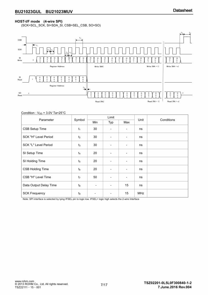
HOST-I/F mode (4-wire SPI) (SCK=SCL_SCK, SI=SDA_SI, CSB=SEL_CSB, SO=SO)
CSB
SIWrite
SCK
W
A
6
W
A
5
W
A
4
W
A
3
W
A
2
W
A
1
W
A
0
W
D
7
W
D
6
W
D
5
W
D
4
W
D
3
W
D
2
W
D
1
W
D
0
W
D
7
W
D
6
W
D
5
W
D
1
W
D
0
Register Address Write (WA + 1)Write (WA) Write (WA + n)
1t
2t 3t
5t4t
7t
SIRead
R
A
6
R
A
5
R
A
4
R
A
3
R
A
2
R
A
1
R
A
0
Register Address
0
1
8t
6t
SORead
R
D
7
R
D
6
R
D
5
R
D
4
R
D
3
R
D
2
R
D
1
R
D
0
R
D
7
R
D
6
R
D
5
R
D
1
R
D
0
Read (RA + 1)Read (RA) Read (RA + n)
z z
9t
Condition : VDD = 3.0V Ta=25°C
Parameter Symbol Limit
Unit Conditions Min Typ Max
CSB Setup Time t1 30 - - ns
SCK "H" Level Period t2 30 - - ns
SCK "L" Level Period t3 30 - - ns
SI Setup Time t4 20 - - ns
SI Holding Time t5 20 - - ns
CSB Holding Time t6 20 - - ns
CSB "H" Level Time t7 50 - - ns
Data Output Delay Time t8 - - 15 ns
SCK Frequency t9 - - 15 MHz
Note: SPI interface is selected by tying IFSEL pin to logic low. IFSEL= logic high selects the 2-wire Interface
BU21023GUL BU21023MUV BU21024FV-M
8/17
TSZ02201-0L5L0F300840-1-2 © 2013 ROHM Co., Ltd. All rights reserved. 7.June.2016 Rev.004
www.rohm.com
TSZ22111・15・001
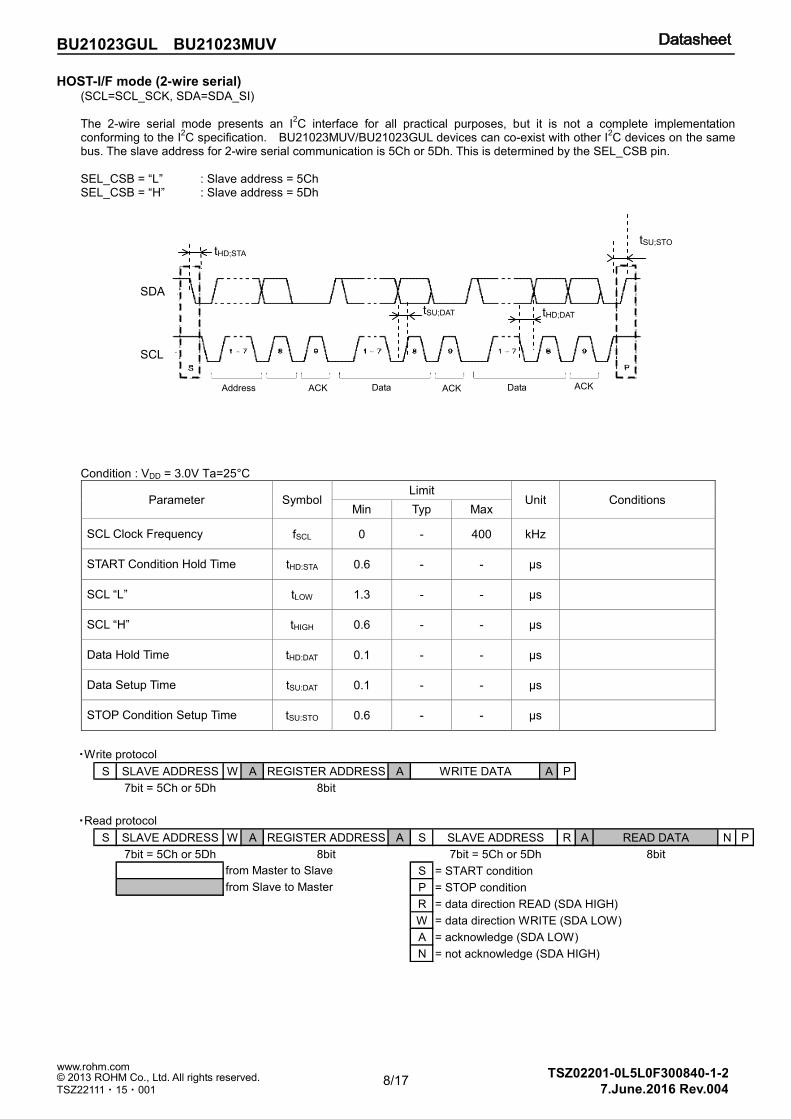
HOST-I/F mode (2-wire serial) (SCL=SCL_SCK, SDA=SDA_SI) The 2-wire serial mode presents an I
2C interface for all practical purposes, but it is not a complete implementation
conforming to the I2C specification. BU21023MUV/BU21023GUL devices can co-exist with other I
2C devices on the same
bus. The slave address for 2-wire serial communication is 5Ch or 5Dh. This is determined by the SEL_CSB pin. SEL_CSB = “L” : Slave address = 5Ch SEL_CSB = “H” : Slave address = 5Dh
Condition : VDD = 3.0V Ta=25°C
Parameter Symbol Limit
Unit Conditions Min Typ Max
SCL Clock Frequency fSCL 0 - 400 kHz
START Condition Hold Time tHD:STA 0.6 - - µs
SCL “L” tLOW 1.3 - - µs
SCL “H” tHIGH 0.6 - - µs
Data Hold Time tHD:DAT 0.1 - - µs
Data Setup Time tSU:DAT 0.1 - - µs
STOP Condition Setup Time tSU:STO 0.6 - - µs
S SLAVE ADDRESS W A REGISTER ADDRESS A A P
7bit = 5Ch or 5Dh 8bit
S SLAVE ADDRESS W A REGISTER ADDRESS A S R A READ DATA N P
7bit = 5Ch or 5Dh 8bit 8bit
S
P
R
W
A
N
= acknowledge (SDA LOW)
= not acknowledge (SDA HIGH)
from Slave to Master = STOP condition
= data direction READ (SDA HIGH)
= data direction WRITE (SDA LOW)
SLAVE ADDRESS
7bit = 5Ch or 5Dh
from Master to Slave = START condition
・Write protocol
WRITE DATA
�
・Read protocol
START
SDA
SCL
STOP
Address Read
/Write
ACK ACK ACK Data Data
tHD;STA tSU;STO
tSU;DAT tHD;DAT
SDA
SCL
BU21023GUL BU21023MUV BU21024FV-M
9/17
TSZ02201-0L5L0F300840-1-2 © 2013 ROHM Co., Ltd. All rights reserved. 7.June.2016 Rev.004
www.rohm.com
TSZ22111・15・001
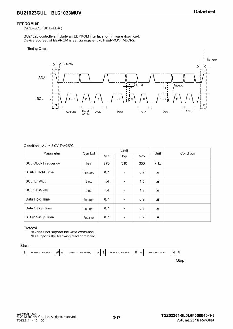
EEPROM I/F (SCL=ECL , SDA=EDA ) BU21023 controllers include an EEPROM interface for firmware download. Device address of EEPROM is set via register 0x51(EEPROM_ADDR). Timing Chart
Condition : VDD = 3.0V Ta=25°C
Parameter Symbol Limit
Unit Condition Min Typ Max
SCL Clock Frequency fSCL 270 310 350 kHz
START Hold Time tHD:STA 0.7 - 0.9 µs
SCL ”L” Width tLOW 1.4 - 1.8 µs
SCL ”H” Width tHIGH 1.4 - 1.8 µs
Data Hold Time tHD:DAT 0.7 - 0.9 µs
Data Setup Time tSU:DAT 0.7 - 0.9 µs
STOP Setup Time tSU:STO 0.7 - 0.9 µs
Protocol
*IC does not support the write command. *IC supports the following read command.
SLAVE ADDRESS W AS
Start
WORD ADDRESS(n) A READ DATA(n)S SLAVE ADDRESS R A N P
Stop
START
SDA
SCL
STOP
Address Read /Write
ACK ACK ACK Data Data
tHD;STA
tSU;STO
tSU;DAT tHD;DAT
BU21023GUL BU21023MUV BU21024FV-M
10/17
TSZ02201-0L5L0F300840-1-2 © 2013 ROHM Co., Ltd. All rights reserved. 7.June.2016 Rev.004
www.rohm.com
TSZ22111・15・001
Background Information A resistive touch screen is made up of multiple layers of sandwiched resistive films and protective coatings all sitting on top of an LCD display. Resistive touch screens work by direct contact of a stylus or a finger flexing a pair of resistive films, hence any blunt pointing instrument or a gloved finger may be used. Touch screen resolution The resolution of a touch screen is typically measured in dots per inch (dpi) and is a function of the physical size of the touch screen and the ADC used in the conversion circuitry. For example, a 3.5 inch x 5 inch screen used with the BU21023 devices can provide a theoretical resolution of 1024 /5 = 204 dpi. In the case of resistive touch screens, the direct contact nature of its operation and finger thickness often impose an upper limit on the effective system resolution that may be achieved, regardless of the resolution of the ADC itself.
Description of Function The BU21023 devices connect to a standard 4-wire resistive touch screen on one side and to a HOST processor on the other side. The BU21023 include the analog and digital circuitry to process and provide dual touch coordinate data and pinch, spread gesture information to the HOST . The BU21023 devices include an internal CPU and provide a high degree of programmability by exposing a set of registers that can be accessed by a HOST through SPI or 2-wire serial interfaces. The IFSEL pin determines whether SPI or 2-wire serial interface is selected, The BU21023 devices include an INT pin whose polarity can be programmed via registers. When an interrupt occurs, for example, due to touch detection, the HOST processor is required to read an interrupt status register to determine the cause of the interrupt and take appropriate action. The program memory of the internal CPU may be initialized via the HOST interface or via an external EEPROM. This is selected by a register setting. The BU21023 devices support two sensing modes; continuous and interval sensing modes, that are register- selectable. In the continuous sensing mode, the embedded CPU reads Z, X & Y coordinates continuously when a touch is detected. The interval sensing mode allows a delay to be inserted between each cycle. The BU21023 devices enable optimization of touch detection threshold for a given screen. They also include several sophisticated calibration algorithms. Often, a description of the registers followed by flow charts requires application note to explain the steps in finer detail. The application note also includes information on touch screen parameters that one should look for when selecting resistive touch screens for multi-touch.
BU21023GUL BU21023MUV BU21024FV-M
11/17
TSZ02201-0L5L0F300840-1-2 © 2013 ROHM Co., Ltd. All rights reserved. 7.June.2016 Rev.004
www.rohm.com
TSZ22111・15・001
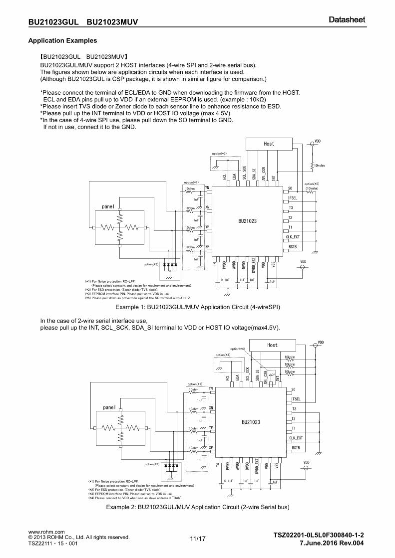
Application Examples
【BU21023GUL BU21023MUV】
BU21023GUL/MUV support 2 HOST interfaces (4-wire SPI and 2-wire serial bus). The figures shown below are application circuits when each interface is used. (Although BU21023GUL is CSP package, it is shown in similar figure for comparison.) *Please connect the terminal of ECL/EDA to GND when downloading the firmware from the HOST. ECL and EDA pins pull up to VDD if an external EEPROM is used. (example : 10kΩ) *Please insert TVS diode or Zener diode to each sensor line to enhance resistance to ESD. *Please pull up the INT terminal to VDD or HOST IO voltage (max 4.5V). *In the case of 4-wire SPI use, please pull down the SO terminal to GND. If not in use, connect it to the GND.
BU21023
Host
T4
PVDD
AVDD
DVDD
DVDD_EXT
VDD
VSS
SEL_CSB
SCL_SCK
SDA_SI
INT
SO
IFSEL
T3
T2
T1
CLK_EXT
RSTB
VDD
VDD
0.1uF 1uF 1uF
10kohm
(10kohm)YN
XN
YP
XP
panel
1nF
1nF
1nF
1nF
10ohm
10ohm
10ohm
10ohm
option(*1)
option(*3)
option(*2)
(*1) For Noise protection RC-LPF. (Please select constant and design for requirement and environment)(*2) For ESD protection. (Zener diode/TVS diode)(*3) EEPROM interface PIN. Please pull-up to VDD in use.(*5) Please pull-down as prevention against the SO terminal output Hi-Z.
option(*5)
EDA
ECL
1uF
Example 1: BU21023GUL/MUV Application Circuit (4-wireSPI)
In the case of 2-wire serial interface use, please pull up the INT, SCL_SCK, SDA_SI terminal to VDD or HOST IO voltage(max4.5V).
(*1) For Noise protection RC-LPF. (Please select constant and design for requirement and environment)(*2) For ESD protection. (Zener diode/TVS diode)(*3) EEPROM interface PIN. Please pull-up to VDD in use.(*4) Please connect to VDD when use as slave address = "BAh".
BU21023
YN
XN
Host
YP
XP
T4
PVDD
AVDD
DVDD
DVDD
_EXT
VDD
VSS
SEL_
CSB
SCL_
SCK
SDA_
SI
EDA
ECL
INT
SO
IFSEL
T3
T2
T1
CLK_EXT
RSTB
VDD
VDD
panel
0.1uF 1uF 1uF
10kohm
10kohm
10kohm
1nF
1nF
1nF
1nF
10ohm
10ohm
10ohm
10ohm
option(*1)
option(*2)
option(*3)
option(*4)
1uF
Example 2: BU21023GUL/MUV Application Circuit (2-wire Serial bus)

BU21023GUL BU21023MUV BU21024FV-M
12/17
TSZ02201-0L5L0F300840-1-2 © 2013 ROHM Co., Ltd. All rights reserved. 7.June.2016 Rev.004
www.rohm.com
TSZ22111・15・001
Operational Notes
1. Reverse Connection of Power Supply
Connecting the power supply in reverse polarity can damage the IC. Take precautions against reverse polarity when connecting the power supply, such as mounting an external diode between the power supply and the IC’s power supply pins.
2. Power Supply Lines
Design the PCB layout pattern to provide low impedance supply lines. Separate the ground and supply lines of the digital and analog blocks to prevent noise in the ground and supply lines of the digital block from affecting the analog block. Furthermore, connect a capacitor to ground at all power supply pins. Consider the effect of temperature and aging on the capacitance value when using electrolytic capacitors.
3. Ground Voltage
Ensure that no pins are at a voltage below that of the ground pin at any time, even during transient condition.
4. Ground Wiring Pattern
When using both small-signal and large-current ground traces, the two ground traces should be routed separately but connected to a single ground at the reference point of the application board to avoid fluctuations in the small-signal ground caused by large currents. Also ensure that the ground traces of external components do not cause variations on the ground voltage. The ground lines must be as short and thick as possible to reduce line impedance.
5. Thermal Consideration
Should by any chance the power dissipation rating be exceeded the rise in temperature of the chip may result in
deterioration of the properties of the chip. The absolute maximum rating of the Pd stated in this specification is when
the IC is mounted on a 70mm x 70mm x 1.6mm glass epoxy board. In case of exceeding this absolute maximum rating,
increase the board size and copper area to prevent exceeding the Pd rating.
6. Recommended Operating Conditions
These conditions represent a range within which the expected characteristics of the IC can be approximately obtained. The electrical characteristics are guaranteed under the conditions of each parameter.
7. Inrush Current
When power is first supplied to the IC, it is possible that the internal logic may be unstable and inrush current may flow instantaneously due to the internal powering sequence and delays, especially if the IC has more than one power supply. Therefore, give special consideration to power coupling capacitance, power wiring, width of ground wiring, and routing of connections.
8. Operation Under Strong Electromagnetic Field
Operating the IC in the presence of a strong electromagnetic field may cause the IC to malfunction.
9. Testing on Application Boards
When testing the IC on an application board, connecting a capacitor directly to a low-impedance output pin may subject the IC to stress. Always discharge capacitors completely after each process or step. The IC’s power supply should always be turned off completely before connecting or removing it from the test setup during the inspection process. To prevent damage from static discharge, ground the IC during assembly and use similar precautions during transport and storage.
10. Inter-pin Short and Mounting Errors
Ensure that the direction and position are correct when mounting the IC on the PCB. Incorrect mounting may result in damaging the IC. Avoid nearby pins being shorted to each other especially to ground, power supply and output pin. Inter-pin shorts could be due to many reasons such as metal particles, water droplets (in very humid environment) and unintentional solder bridge deposited in between pins during assembly to name a few.
BU21023GUL BU21023MUV BU21024FV-M
13/17
TSZ02201-0L5L0F300840-1-2 © 2013 ROHM Co., Ltd. All rights reserved. 7.June.2016 Rev.004
www.rohm.com
TSZ22111・15・001
Operational Notes - continued
11. Unused Input Pins
Input pins of an IC are often connected to the gate of a MOS transistor. The gate has extremely high impedance and extremely low capacitance. If left unconnected, the electric field from the outside can easily charge it. The small charge acquired in this way is enough to produce a significant effect on the conduction through the transistor and cause unexpected operation of the IC. So unless otherwise specified, unused input pins should be connected to the power supply or ground line.
12. Regarding the Input Pin of the IC
In the construction of this IC, P-N junctions are inevitably formed creating parasitic diodes or transistors. The operation of these parasitic elements can result in mutual interference among circuits, operational faults, or physical damage. Therefore, conditions which cause these parasitic elements to operate, such as applying a voltage to an input pin lower than the ground voltage should be avoided. Furthermore, do not apply a voltage to the input pins when no power supply voltage is applied to the IC. Even if the power supply voltage is applied, make sure that the input pins have voltages within the values specified in the electrical characteristics of this IC.
13. Ceramic Capacitor
When using a ceramic capacitor, determine the dielectric constant considering the change of capacitance with temperature and the decrease in nominal capacitance due to DC bias and others.
14. Others
In case of use this IC, please peruse some other detail documents, we called Functional description, Application note.
BU21023GUL BU21023MUV BU21024FV-M
14/17
TSZ02201-0L5L0F300840-1-2 © 2013 ROHM Co., Ltd. All rights reserved. 7.June.2016 Rev.004
www.rohm.com
TSZ22111・15・001
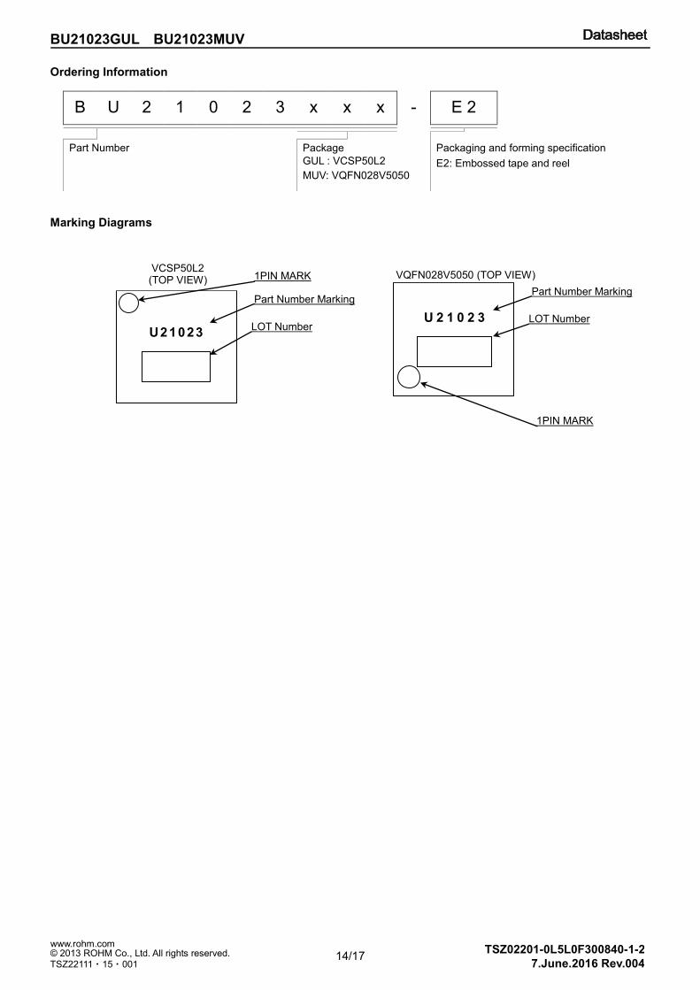
Ordering Information
B U 2 1 0 2 3 x x x - E 2
Part Number
Package
GUL : VCSP50L2
MUV: VQFN028V5050
Packaging and forming specification
E2: Embossed tape and reel
Marking Diagrams
1PIN MARK
VQFN028V5050 (TOP VIEW)
U 2 1 0 2 3
Part Number Marking
LOT Number
VCSP50L2 (TOP VIEW)
U21023
Part Number Marking
LOT Number
1PIN MARK
BU21023GUL BU21023MUV BU21024FV-M
15/17
TSZ02201-0L5L0F300840-1-2 © 2013 ROHM Co., Ltd. All rights reserved. 7.June.2016 Rev.004
www.rohm.com
TSZ22111・15・001
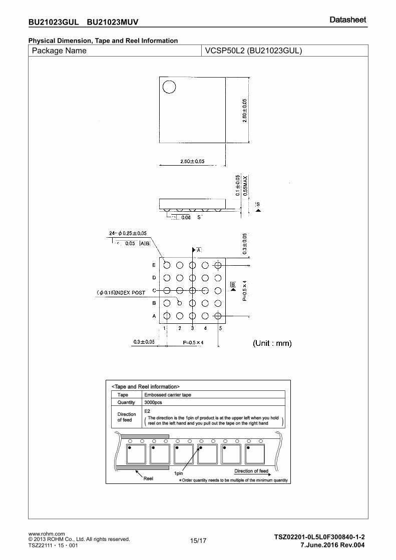
Physical Dimension, Tape and Reel Information
Package Name VCSP50L2 (BU21023GUL)
BU21023GUL BU21023MUV BU21024FV-M
16/17
TSZ02201-0L5L0F300840-1-2 © 2013 ROHM Co., Ltd. All rights reserved. 7.June.2016 Rev.004
www.rohm.com
TSZ22111・15・001
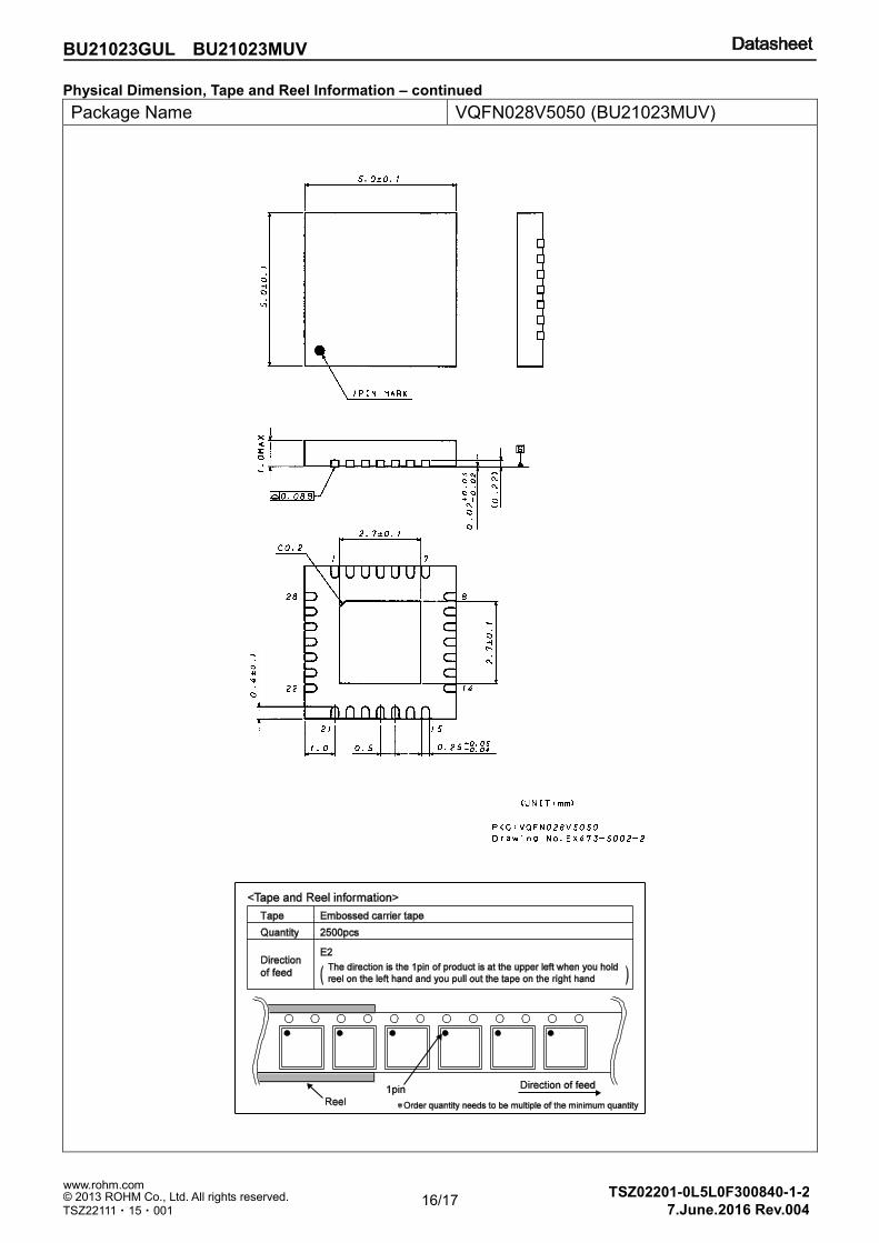
Physical Dimension, Tape and Reel Information – continued
Package Name VQFN028V5050 (BU21023MUV)
BU21023GUL BU21023MUV BU21024FV-M
17/17
TSZ02201-0L5L0F300840-1-2 © 2013 ROHM Co., Ltd. All rights reserved. 7.June.2016 Rev.004
www.rohm.com
TSZ22111・15・001
Revision History
Date Revision Changes
07.Oct.2013 001 New Release
07.Feb.2014 002 Remove the description of BU21024FV-M Added 3D package image
17.Mar.2014 003 Change description p10 from “other document” to “application note”.
7.June.2016 004
P1 fix miss description Features (old) I
2C
(new) 2-wire serial P1 fix miss description Key Specifications and Lineup (old) Pakage (new) Package P3 Add the description of the thermal PAD connection. P5 fix miss description (old) 2-wire I
2C
(new) 2-wire serial P6 fix miss description PCB(1 layer) (old) 70x70x1.6mm
3
(new) 74.2x74.2x1.6t mm. P8 Add condition description (new) Condition : VDD = 3.0V Ta=25°C P9 Add condition description (new) Condition : VDD = 3.0V Ta=25°C P10 fix miss description
(old) For example, a 3”x5” screen used (new) For example, a 3.5 inch x 5 inch screen used
P10 fix miss description (old) I
2C
(new) 2-wire serial P11 Application Examples Example 1: BU21023GUL/MUV Application Circuit (4-wireSPI) Add 1uF (VDD-VSS) as bypass capacitor. Change the circuit symbol of TVS diode. Add annotations. Example 2: BU21023GUL/MUV Application Circuit (2-wire Serial bus) Add 1uF (VDD-VSS) as bypass capacitor. Change the circuit symbol of TVS diode. Add annotations.

Notice-PGA-E Rev.003
© 2015 ROHM Co., Ltd. All rights reserved.
Notice
Precaution on using ROHM Products 1. Our Products are designed and manufactured for application in ordinary electronic equipments (such as AV equipment,
OA equipment, telecommunication equipment, home electronic appliances, amusement equipment, etc.). If you intend to use our Products in devices requiring extremely high reliability (such as medical equipment
(Note 1), transport
equipment, traffic equipment, aircraft/spacecraft, nuclear power controllers, fuel controllers, car equipment including car accessories, safety devices, etc.) and whose malfunction or failure may cause loss of human life, bodily injury or serious damage to property (“Specific Applications”), please consult with the ROHM sales representative in advance. Unless otherwise agreed in writing by ROHM in advance, ROHM shall not be in any way responsible or liable for any damages, expenses or losses incurred by you or third parties arising from the use of any ROHM’s Products for Specific Applications.
(Note1) Medical Equipment Classification of the Specific Applications
JAPAN USA EU CHINA
CLASSⅢ CLASSⅢ
CLASSⅡb CLASSⅢ
CLASSⅣ CLASSⅢ
2. ROHM designs and manufactures its Products subject to strict quality control system. However, semiconductor
products can fail or malfunction at a certain rate. Please be sure to implement, at your own responsibilities, adequate safety measures including but not limited to fail-safe design against the physical injury, damage to any property, which a failure or malfunction of our Products may cause. The following are examples of safety measures:
[a] Installation of protection circuits or other protective devices to improve system safety [b] Installation of redundant circuits to reduce the impact of single or multiple circuit failure
3. Our Products are designed and manufactured for use under standard conditions and not under any special or extraordinary environments or conditions, as exemplified below. Accordingly, ROHM shall not be in any way responsible or liable for any damages, expenses or losses arising from the use of any ROHM’s Products under any special or extraordinary environments or conditions. If you intend to use our Products under any special or extraordinary environments or conditions (as exemplified below), your independent verification and confirmation of product performance, reliability, etc, prior to use, must be necessary:
[a] Use of our Products in any types of liquid, including water, oils, chemicals, and organic solvents [b] Use of our Products outdoors or in places where the Products are exposed to direct sunlight or dust [c] Use of our Products in places where the Products are exposed to sea wind or corrosive gases, including Cl2,
H2S, NH3, SO2, and NO2
[d] Use of our Products in places where the Products are exposed to static electricity or electromagnetic waves [e] Use of our Products in proximity to heat-producing components, plastic cords, or other flammable items [f] Sealing or coating our Products with resin or other coating materials [g] Use of our Products without cleaning residue of flux (even if you use no-clean type fluxes, cleaning residue of
flux is recommended); or Washing our Products by using water or water-soluble cleaning agents for cleaning residue after soldering
[h] Use of the Products in places subject to dew condensation
4. The Products are not subject to radiation-proof design. 5. Please verify and confirm characteristics of the final or mounted products in using the Products. 6. In particular, if a transient load (a large amount of load applied in a short period of time, such as pulse. is applied,
confirmation of performance characteristics after on-board mounting is strongly recommended. Avoid applying power exceeding normal rated power; exceeding the power rating under steady-state loading condition may negatively affect product performance and reliability.
7. De-rate Power Dissipation depending on ambient temperature. When used in sealed area, confirm that it is the use in
the range that does not exceed the maximum junction temperature. 8. Confirm that operation temperature is within the specified range described in the product specification. 9. ROHM shall not be in any way responsible or liable for failure induced under deviant condition from what is defined in
this document.
Precaution for Mounting / Circuit board design 1. When a highly active halogenous (chlorine, bromine, etc.) flux is used, the residue of flux may negatively affect product
performance and reliability.
2. In principle, the reflow soldering method must be used on a surface-mount products, the flow soldering method must be used on a through hole mount products. If the flow soldering method is preferred on a surface-mount products, please consult with the ROHM representative in advance.
For details, please refer to ROHM Mounting specification

Notice-PGA-E Rev.003
© 2015 ROHM Co., Ltd. All rights reserved.
Precautions Regarding Application Examples and External Circuits 1. If change is made to the constant of an external circuit, please allow a sufficient margin considering variations of the
characteristics of the Products and external components, including transient characteristics, as well as static characteristics.
2. You agree that application notes, reference designs, and associated data and information contained in this document
are presented only as guidance for Products use. Therefore, in case you use such information, you are solely responsible for it and you must exercise your own independent verification and judgment in the use of such information contained in this document. ROHM shall not be in any way responsible or liable for any damages, expenses or losses incurred by you or third parties arising from the use of such information.
Precaution for Electrostatic This Product is electrostatic sensitive product, which may be damaged due to electrostatic discharge. Please take proper caution in your manufacturing process and storage so that voltage exceeding the Products maximum rating will not be applied to Products. Please take special care under dry condition (e.g. Grounding of human body / equipment / solder iron, isolation from charged objects, setting of Ionizer, friction prevention and temperature / humidity control).
Precaution for Storage / Transportation 1. Product performance and soldered connections may deteriorate if the Products are stored in the places where:
[a] the Products are exposed to sea winds or corrosive gases, including Cl2, H2S, NH3, SO2, and NO2 [b] the temperature or humidity exceeds those recommended by ROHM [c] the Products are exposed to direct sunshine or condensation [d] the Products are exposed to high Electrostatic
2. Even under ROHM recommended storage condition, solderability of products out of recommended storage time period may be degraded. It is strongly recommended to confirm solderability before using Products of which storage time is exceeding the recommended storage time period.
3. Store / transport cartons in the correct direction, which is indicated on a carton with a symbol. Otherwise bent leads
may occur due to excessive stress applied when dropping of a carton. 4. Use Products within the specified time after opening a humidity barrier bag. Baking is required before using Products of
which storage time is exceeding the recommended storage time period.
Precaution for Product Label A two-dimensional barcode printed on ROHM Products label is for ROHM’s internal use only.
Precaution for Disposition When disposing Products please dispose them properly using an authorized industry waste company.
Precaution for Foreign Exchange and Foreign Trade act Since concerned goods might be fallen under listed items of export control prescribed by Foreign exchange and Foreign trade act, please consult with ROHM in case of export.
Precaution Regarding Intellectual Property Rights 1. All information and data including but not limited to application example contained in this document is for reference
only. ROHM does not warrant that foregoing information or data will not infringe any intellectual property rights or any other rights of any third party regarding such information or data.
2. ROHM shall not have any obligations where the claims, actions or demands arising from the combination of the Products with other articles such as components, circuits, systems or external equipment (including software).
3. No license, expressly or implied, is granted hereby under any intellectual property rights or other rights of ROHM or any third parties with respect to the Products or the information contained in this document. Provided, however, that ROHM will not assert its intellectual property rights or other rights against you or your customers to the extent necessary to manufacture or sell products containing the Products, subject to the terms and conditions herein.
Other Precaution 1. This document may not be reprinted or reproduced, in whole or in part, without prior written consent of ROHM.
2. The Products may not be disassembled, converted, modified, reproduced or otherwise changed without prior written consent of ROHM.
3. In no event shall you use in any way whatsoever the Products and the related technical information contained in the Products or this document for any military purposes, including but not limited to, the development of mass-destruction weapons.
4. The proper names of companies or products described in this document are trademarks or registered trademarks of ROHM, its affiliated companies or third parties.
DatasheetDatasheet
Notice – WE Rev.001© 2015 ROHM Co., Ltd. All rights reserved.
General Precaution 1. Before you use our Pro ducts, you are requested to care fully read this document and fully understand its contents.
ROHM shall n ot be in an y way responsible or liabl e for fa ilure, malfunction or acci dent arising from the use of a ny ROHM’s Products against warning, caution or note contained in this document.
2. All information contained in this docume nt is current as of the issuing date and subj ect to change without any prior
notice. Before purchasing or using ROHM’s Products, please confirm the la test information with a ROHM sale s representative.
3. The information contained in this doc ument is provi ded on an “as is” basis and ROHM does not warrant that all
information contained in this document is accurate an d/or error-free. ROHM shall not be in an y way responsible or liable for any damages, expenses or losses incurred by you or third parties resulting from inaccuracy or errors of or concerning such information.


![Touch Technologies Tutorial · Emerging Touch Technologies With Multi-Touch [58] Projected Capacitive LCD In-Cell (Optical, Switch & Capacitive) Optical Digital Resistive Waveguide](https://static.fdocuments.net/doc/165x107/6000f3e8fa24967a0f056959/touch-technologies-tutorial-emerging-touch-technologies-with-multi-touch-58-projected.jpg)


