Research on Electrical Discharge Machining of...
53
Research on Electrical Discharge Machining of Polycrystalline Diamond A thesis submitted in fulfilment of the requirements for the degree of Doctor of Philosophy Mohammad Zulafif Rahim M. Eng. (Advanced Manufacturing Technology) B. Eng. (Hons) (Mechanical-Manufacturing) School of Aerospace Mechanical and Manufacturing Engineering College of Science Engineering and Health RMIT University June 2015
Transcript of Research on Electrical Discharge Machining of...
Research on Electrical Discharge
Machining of Polycrystalline
Diamond
A thesis submitted in fulfilment of the requirements for the degree of Doctor of Philosophy
Mohammad Zulafif Rahim
M. Eng. (Advanced Manufacturing Technology)
B. Eng. (Hons) (Mechanical-Manufacturing)
School of Aerospace Mechanical and Manufacturing Engineering
College of Science Engineering and Health
RMIT University
June 2015
iv
Abstract
The non-contact process of Electrical Discharge Machining (EDM) eliminates
cutting forces, and is regarded as the most effective process to machine
polycrystalline diamond (PCD). However, the EDM plasma temperature of up to
12000K in the EDM process will cause damage to the machined surface. With
emphasis on the cutting tool product, this study focuses on the analysis of the PCD
surface damage caused by the Electrical Discharge Grinding (EDG) process and its
optimization strategies. In addition to the graphitization and residual stress, several
issues that assumed to be thermal damage indications caused by the process are
highlighted. These include the formation of porous surfaces, cutting edge undercuts
and some cosmetic aspects at the WC-PCD interface. It was found that the high
temperature generated during erosion resulted in the partial conversion of diamond to
graphite phase under the surface. Higher finishing in-feed proved to produce better
surface quality by means of lower surface graphitization and lower tensile residual
stress. The comprehensive discussion undertaken includes the theoretical modelling
of the process, together with the validated results. The structural difference and
residual stress between PCD manufactured with EDG and conventional grinding
have been compared. Performance tests have also been conducted at the end of the
methodology to evaluate and validate the models.
ix
Table of Contents
Declaration ................................................................................................................... ii
Abstract ....................................................................................................................... iv
Acknowledgements ...................................................................................................... v
Publications ................................................................................................................. vi
List of Figures ............................................................................................................ xii
List of Tables............................................................................................................ xvii
Symbols ................................................................................................................... xviii
Chapter 1 Introduction ................................................................................................. 1
1.1. Research Background .................................................................................... 1
1.2. Objectives and Research Questions............................................................... 3
1.3. Scope of the Investigation ............................................................................. 5
1.4. Challenges in PCD Tools Fabrication ........................................................... 6
1.5. Research Methodology .................................................................................. 8
Chapter 2 Literature Review ...................................................................................... 10
2.1. Introduction ................................................................................................. 10
2.2. PCD EDM Process ...................................................................................... 11
2.2.1. EDM Polarity .......................................................................................... 12
2.2.2. Material Removal Rate ............................................................................ 15
2.2.3. Surface Roughness and Morphology ....................................................... 17
2.2.4. Challenges on Cutting of Laminar Discs ................................................. 21
2.2.5. Heat Affected Zone (HAZ) ...................................................................... 22
2.2.6. Material Phase Transformation ................................................................ 25
2.3. Conclusion ................................................................................................... 28
Chapter 3 Experiment Procedure and Method of Analysis ........................................ 29
3.1. Introduction ................................................................................................. 29
3.2. Electrical Discharge Grinding Process ........................................................ 29
3.3. Raman analysis ............................................................................................ 33
3.4. XRD Analysis .............................................................................................. 37
3.5. XRD vs. Raman analysis in Residual Stress and Graphitization Analysis . 39
3.6. Conclusion ................................................................................................... 41

x
Chapter 4 Investigation on the Effect of Electrode Polarity ...................................... 42
4.1. Introduction ................................................................................................. 42
4.2. Experimental Procedure .............................................................................. 43
4.3. Result and Discussion.................................................................................. 48
4.3.1. Morphological Analysis ........................................................................... 48
4.3.2. Material Removal Rate ............................................................................ 55
4.4. Conclusion ................................................................................................... 62
Chapter 5 Investigation on the Effect of Wheel Rotation Direction .......................... 64
5.1. Introduction ................................................................................................. 64
5.2. Equipment and Methodology ...................................................................... 66
5.3. Results and Discussion ................................................................................ 70
5.4. Conclusion ................................................................................................... 81
Chapter 6 Investigation on the Effect of Machining Parameters and Its Theoretical
Modelling ................................................................................................................... 83
6.1. Introduction ................................................................................................. 83
6.2. Equipment and Methodology ...................................................................... 85
6.3. Results and Discussion ................................................................................ 87
6.3.1. Effect of Roughing Process ..................................................................... 87
6.3.2. Theoretical Model .................................................................................... 93
6.3.3. Effect of Finishing Operation ................................................................ 105
6.3.4. Single Discharge Test ............................................................................ 111
6.4. Conclusion ................................................................................................. 114
Chapter 7 Tool Quality Investigation and Performance Analysis ........................... 116
7.1. Introduction ............................................................................................... 116
7.2. Methodology.............................................................................................. 118
7.2.1. Conventional Grinding Parameter Selection ......................................... 118
7.2.2. EDG Machining Parameters Selection .................................................. 120
7.2.3. Morphological, Structural Quality, and Residual Stress Analysis......... 121
7.2.4. Performance Analysis ............................................................................ 122
7.3. Results and Discussion .............................................................................. 123
7.3.1. Morphological Analysis ......................................................................... 123
7.3.2. Residual Stress and Graphitization Analysis ......................................... 127
7.3.3. Performance Test ................................................................................... 133
xi
7.4. Conclusion ................................................................................................. 141
Chapter 8 Tool Quality Assessment and Validation ................................................ 143
8.1. Introduction ............................................................................................... 143
8.2. Methodology.............................................................................................. 144
8.3. Result and Discussion................................................................................ 146
8.4. Conclusion ................................................................................................. 154
Chapter 9 Summary.................................................................................................. 155
9.1. Summary.................................................................................................... 155
9.2. Future Work............................................................................................... 159
9.2.1. Investigation on Material Removal Rate ............................................... 159
9.2.2. Mathematical modelling of thermal residual stress ............................... 159
9.2.3. An extensive investigation on PCD tool invisible quality ..................... 160
References ................................................................................................................ 161
xii
List of Figures
Figure 1: Example of special geometry drill-bit commercially available in machining
of fibre reinforced plastic material [7] ......................................................................... 2
Figure 2: Weekly tool usage in Boeing Aerostructures Australia................................ 4
Figure 3: PCD tool. ...................................................................................................... 6
Figure 4: Edge undercut ............................................................................................... 7
Figure 5: Research methodology ................................................................................. 8
Figure 6: Illustration of the process flow ..................................................................... 8
Figure 7: Graphite Coating Method ........................................................................... 12
Figure 8: Comparison of electrode shape obtained by SEM after different polarity
machining. (a) Initial shape of electrode (before machining) (b) Electrode after the
positive polarity erosion (positive polarity of the tool electrode) (c) Electrode shape
after negative polarity erosion (negative polarity of the tool electrode)[6] ............... 14
Figure 9: MRR optimization strategies ...................................................................... 16
Figure 10:EDMed surfaces of boron doped PCD sample[53] ................................... 19
Figure 11: Void due to selective erosion [59] ............................................................ 21
Figure 12: Element Mapping of (a) C, (b) Co, (c) Ta and (d) W [62] ....................... 22
Figure 13: Heat affected zone of EDMed surface [58] .............................................. 23
Figure 14: SEM image of PCD (a) after EDM (b) after LWJ [65, 66] ...................... 24
Figure 15: PCD structure [21] .................................................................................... 25
Figure 16: Carbon phase diagram [10]....................................................................... 26
Figure 17: Distribution of chemical elements close to the EDMed edge[59] ............ 27
Figure 18:RX7 EDG machine .................................................................................... 30
Figure 19: Schematic of the EDG process ................................................................. 30
Figure 20: Discharge phases in EDM [87] ................................................................. 31
Figure 21: EDG equipment (a) Pulse generator (b) Data acquisition system ............ 33
Figure 22: Raman spectra result on composition of electrode (A) before EDM, (B)
after EDM [6] ............................................................................................................. 35
Figure 23: SEM image of 10µm synthetic diamond particles. .................................. 36
Figure 24:Raman spectra of the unstressed diamond grains ...................................... 36
Figure 25: Experimental setup and procedure ........................................................... 46
Figure 26: Block diagram of the EDM gap control system ....................................... 47
xiii
Figure 27: Surface produced by finishing operation. (a) Negative polarity. ............. 48
Figure 28: Close up view of the surfaces produced. (a) Negative polarity. ............... 49
Figure 29: EDX surface mapping .............................................................................. 49
Figure 30: Elemental composition (a) Negative polarity, (b) Positive polarity ......... 51
Figure 31:XRD analysis of the surface eroded with different polarities (a) Negative
polarity, (b) Positive polarity ..................................................................................... 52
Figure 32: Raman Analysis: (a) Raman shift value, (b) FWHM analysis of the
Raman spectrum ......................................................................................................... 54
Figure 33: Illustration of the black layer assisted erosion theory .............................. 55
Figure 34: Material erosion rate of different PCD types (positive polarity) .............. 56
Figure 35: Material erosion rate of different PCD types (negative polarity) ............. 57
Figure 36: Residue surface left by the roughing surface: (a) SEM image (CTB010),
(b) Surface profile (CTX002), (c) Surface profile (CTB010), (d) Surface profile
(CTM302) .................................................................................................................. 58
Figure 37: Non-linear regression line fitting .............................................................. 59
Figure 38: The images of deposited material on the eroded surface of CTM302 PCD
(obtained by the optical microscope with 100x magnification lens): (a) After 10µm
finishing in-feed; (b) After 20µm finishing in-feed; (c) After 30µm finishing in-
feed; (d) After 40µm finishing in-feed ...................................................................... 60
Figure 39: SEM image of the black layer .................................................................. 60
Figure 40: Elemental composition of the black layer (The image taken is
perpendicular from the eroded surface) ..................................................................... 61
Figure 41: MRR versus wheel speed ......................................................................... 67
Figure 42:Experimental methodology (wheel direction): (a) Counter-clockwise
(ccw), (b) Clockwise (cw), (c) Actual EDG process ................................................. 68
Figure 43: Specimen: (a) Description of the specimen; (b) PCD strip (before
erosion); (c) Specimen with 50º apex angle (after erosion) ....................................... 69
Figure 44: Measurement method: (a) Alicona optical measuring device used in the
experiment; (b) 3D image of the PCD edge obtained by Alicona; (c) Position of
extracted profile paths for tool sharpness measurement ............................................ 70
Figure 45: Definition of sharpness parameter. ........................................................... 70
Figure 46: Comparison between Sa and Sy obtained by two different methods, which
are WC to PCD (ccw wheel rotation) and PCD to WC (cw wheel rotation) ............. 71
xiv
Figure 47: Effect of wheel rotation on the edge radius and symmetry (1=symmetry)
.................................................................................................................................... 72
Figure 48: Schematic of fluid flow under a moving plate ......................................... 73
Figure 49: SEM image of the eroded surface using different wheel rotation direction:
(a) ccw wheel rotation direction (300x magnification); (b) cw wheel direction (300x
magnification); (c) ccw wheel direction (2000x magnifications); (d) cw wheel
direction (2000x magnification); (e) Illustration of the spark concentration
phenomenon ............................................................................................................... 74
Figure 50: Undercut formed due to continuous uneven sparking on the PCD edge
(image taken from the eroded surface)....................................................................... 75
Figure 51: Extraction position for the edge roughness measurement ........................ 75
Figure 52: The roughness (Ra) of PCD edges measured by Alicona device ............. 76
Figure 53: SEM image of the cutting edge produced (images taken from the polished
surface): (a) 90 degree apex angle with cw wheel direction; (b) 70 degree apex angle
with cw wheel direction; (c) 50 degree apex angle with cw wheel direction; (d) 90
degree apex angle with ccw wheel direction; (e) 70 degree apex angle with ccw
wheel direction; (e) 50 degree apex angle with ccw wheel direction ........................ 77
Figure 54: Results of Raman analysis ........................................................................ 78
Figure 55: Effect of higher wheel speed .................................................................... 78
Figure 56: 3D images of the eroded surface: (a) cw wheel direction; (b) ccw wheel
direction...................................................................................................................... 79
Figure 57: Cross-section profile of the surface: (a) cw wheel direction; (b) ccw wheel
direction...................................................................................................................... 79
Figure 58: Notch size ................................................................................................ 80
Figure 59: Illustration of the electrolyte flow and debris accomulation: (a) cw wheel
direction; (b) ccw wheel direction; (c) Actual image of the notch ............................ 81
Figure 60: Three stages of the residual stress formation in tool production .............. 83
Figure 61: SEM images of the PCD after roughing (modified zone was clearly
observed on the 12A PCD sample) ............................................................................ 88
Figure 62: SEM and Backscatter Image of modified zone ........................................ 89
Figure 63: Raman analysis ......................................................................................... 89
Figure 64: SEM images (left) and backscatter images (right) of the eroded PCD by
roughing ..................................................................................................................... 92

xv
Figure 65: Inspection location (the collected debris was deposited on the carbon tape)
.................................................................................................................................... 92
Figure 66:Thermal stress components considered in the model(r = position where the
stress is estimated, a = diamond grain radius, σ = stress component for tangential, t
and radial, r direction) [86] ........................................................................................ 93
Figure 67: Temperature-dependent properties of diamond ........................................ 97
Figure 68: Current, voltage, spark radius, and heat flux value used in the model ..... 99
Figure 69: Scheme for the boundary conditions ...................................................... 100
Figure 70: Temperature-dependent properties calculated ........................................ 102
Figure 71: Temperature-stress relationship for different PCD ................................ 104
Figure 72: Diamond breakage mechanism ............................................................... 105
Figure 73: Eroded surface by the finishing operation .............................................. 106
Figure 74: Raman D-value (a) CTX002 (b) CTB010 (c) CTM302 ......................... 108
Figure 75: D/G ratio (a) CTX002 (b) CTB010 (c) CTM302 ................................... 110
Figure 76: A comparison of graphitization degree of three different PCD.............. 111
Figure 77: Current, voltage, spark radius, and heat flux value used in the model ... 112
Figure 78: The profile of two craters (a) and (b) on the PCD surface ..................... 113
Figure 79: ANSYS simulation result ....................................................................... 114
Figure 80: Grinding process of PCD: (a) Machine setup; (b) PCD insert holder .... 119
Figure 81: EDG process of PCD: (a) Machine setup; (b) PCD insert holder .......... 120
Figure 82: Experimental setup ................................................................................. 123
Figure 83: Surface roughness: (a) CTX002 ground surface; (b) CTB010 ground
surface; (c) CTX302 ground surface; (d) Eroded surface ........................................ 124
Figure 84: SEM Images of CTB010: (a) Eroded PCD; (b) Ground PCD ................ 125
Figure 85: Cutting edge radius: (a) CTX002 ground surface; (b) CTB010 ground
surface; (c) CTX302 ground surface; (d) Eroded surface ........................................ 126
Figure 86: SEM image of the cutting edge CTB010 prepared by different methods:
(a) EDG erosion; (b) Conventionally ground with 10m/s wheel velocity 5µm in-feed
.................................................................................................................................. 127
Figure 87: Raman value of the Ground PCD: (a)CTX002 ground surface; (b)
CTB010 ground surface; (c) CTX302 ground surface; (d) Eroded surface ............. 129
Figure 88: Raman spectra of ground polycrystalline diamond ................................ 131
Figure 89: Raman spectra of eroded polycrystalline diamond................................. 132
xvi
Figure 90: 3D images of the worn cutting tools, grooves prepared by specific PCD
tools insert and their cross-sectional profile: (a) Eroded CTB010 (10µm finishing in-
feed); (b) Eroded CTB010 (40µm finishing in-feed); (c) Ground CTB010 (10m/s
machining velocity, 0.2mm/min feed rate) .............................................................. 134
Figure 91: Wear mode of the cutting tools (CTX002): (a) Eroded (10µm finishing in-
feed); (b) Eroded (40µm finishing in-feed); (c) Ground .......................................... 135
Figure 92: Wear mode of the cutting tools (CTB010): (a) Eroded (10µm finishing in-
feed); (b) Eroded (40µm finishing in-feed); (c) Ground .......................................... 136
Figure 93: Wear mode of the cutting tools: (CTM302) (a) Eroded (10µm finishing
in-feed); (b) Eroded (40µm finishing in-feed); (c) Ground ..................................... 137
Figure 94: EDX spectrum of point A ....................................................................... 138
Figure 95: Relationship between sharpness and cutting force: (a) Used cutting edge;
(b) z-direction cutting force value ............................................................................ 139
Figure 96: Cutting tip shortening and their effect on the cutting force .................... 139
Figure 97: Cutting force produced by ground PCD ................................................. 140
Figure 98: Experimental setup for the turning test................................................... 145
Figure 99: Raman analysis of the PCD surface ....................................................... 146
Figure 100: Flank wear after each stage of turning experiment............................... 147
Figure 101: PCD tools after 30 seconds of the turning process: (a) 3-stage PCD; (b)
2-stage PCD; (c) Ground PCD ................................................................................. 150
Figure 102: PCD tools after 10 minutes of the turning process: (a) 3-stage PCD; (b)
2-stage PCD; (c) Ground PCD ................................................................................. 151
Figure 103: PCD nose wear and their effect to the chip formation after 10 minutes of
the turning process: (a) 3-stage eroded PCD; (b) 2-stage eroded PCD; (c) Ground
PCD .......................................................................................................................... 152
Figure 104: Work piece surface after 1 minute machining: (a) 3-stage eroded PCD;
(b) 2-stage eroded PCD; (c) Ground PCD ............................................................... 153
Figure 105: Work piece surface after 10 minute‘s machining: (a) 3-stage eroded
PCD; (b) 2-stage eroded PCD; (c) Ground PCD ..................................................... 153
xvii
List of Tables
Table 1: Erosion resistance index (ERI) of materials [6] ........................................... 15
Table 2: Comparison between PCD and CVDITE CDE material ............................. 18
Table 3: Peak band centre for the Raman analysis as carbon lattice structure
identification [6, 83, 90] ............................................................................................. 34
Table 4: Overview of selected literatures................................................................... 39
Table 5: Finishing strategies ...................................................................................... 43
Table 6: Properties of PCD [98-100] ......................................................................... 44
Table 7: EDG machining parameters ......................................................................... 44
Table 8: EDG parameters for specimen preparation .................................................. 66
Table 9: EDG parameters for the roughing experiment ............................................. 86
Table 10: Properties of PCD [98-100] ....................................................................... 86
Table 11: EDG parameters for the finishing experiment ........................................... 87
Table 12: Properties of diamond and cobalt .............................................................. 96
Table 13: Comparative study between the theoretical values obtained from the
physical model and the real value ............................................................................ 109
Table 14: Properties of PCD [98-100] ..................................................................... 118
Table 15: EDG machining parameters ..................................................................... 121
Table 16: Properties of Ti-6Al-4V used................................................................... 144
Table 17: Chemical composition of the work piece................................................. 144
Table 18: 3-stage erosion parameters ....................................................................... 145
xviii
Symbols
A cross sectional area (mm2)
a diamond grain radius (µm)
C specific heat of material (J/kgK)
Cm erosion resistance index (1012
J2/ m s kg)
cc heat capacitance for cobalt (J/kgK)
cd heat capacitance for diamond (J/kgK)
d lattice spacing (nm)
E modulus of elasticity (N/m2)
Ed discharge energy (J)
ε strain
fc cobalt fraction
fd diamond fraction
h sparking gap distance (µm)
i current (A)
K thermal conductivity (W/mK)
kd thermal conductivity of diamond (W/mK)
kc thermal conductivity of cobalt (W/mK)
ṁ volume erosion rate (mm3/s)
q heat flux (J/s)
r position where the stress value is determined (µm)
rp plasma radius (µm)
ṡ feed rate (mm/s)
T temperature (K)
Tm melting point (K)
t pulse duration (µs)
U voltage (V)
u thermal displacement (µm)
V viscosity (kg/ms)
xix
v Poisson‘s ratio
νr unstressed Raman value (cm-1
)
νs Raman shift value (cm-1
)
χ coefficient of stress-induced frequency shift (N/m2)
α coefficient of thermal expansion (K-1
)
θ temperature difference (K)
θc X-ray diffraction angle (degree, o)
λ elastic modulus
λc X-ray wavelength (nm)
µ shear modulus
σ tensile residual stress (N/m2)
σt tangential stress (N/m2)
σt radial stress (N/m2)
Ψ X-ray diffraction tilt angle (degree, o)
Chapter 1 Introduction
1.1.Research Background
Known as a hard and brittle material, polycrystalline diamond (PCD) is produced
from diamond particles that are sintered together under high temperature and high
pressure conditions (at temperatures of 1670K to 1770K and pressures of 5GPa to
6GPa) in the presence of a catalytic metal [1-4]. PCD is becoming popular because
of its excellent physical characteristics. It has been applied widely in die and cutting
tool applications due to the high hardness, good thermal conductivity, high strength,
and chemical resistance to most corrosive environments [5, 6]. Until 1996,
applications of PCD tools were monopolized by the automotive sector due to the
limitations of the process, which is efficient only in forming simple shapes [1].
Conventionally abrasive grinding processes have been established as the fabricating
method for PCD cutting tools. Although better surface roughness can be obtained by
conventional grinding, low grinding efficiency and large grinding forces induced
during the process are inherent problems that limit the wide application of PCD
tools. The non-contact process of Electric Discharge Machining (EDM) eliminates
cutting forces, and is regarded as the process that will result in a better application by
means of process flexibility with lower production costs [6]. For this reason,
nowadays, further investigation on EDM of PCD is becoming extensive, and EDM is
expected to be the best strategy in integrating the complicated geometric shape and
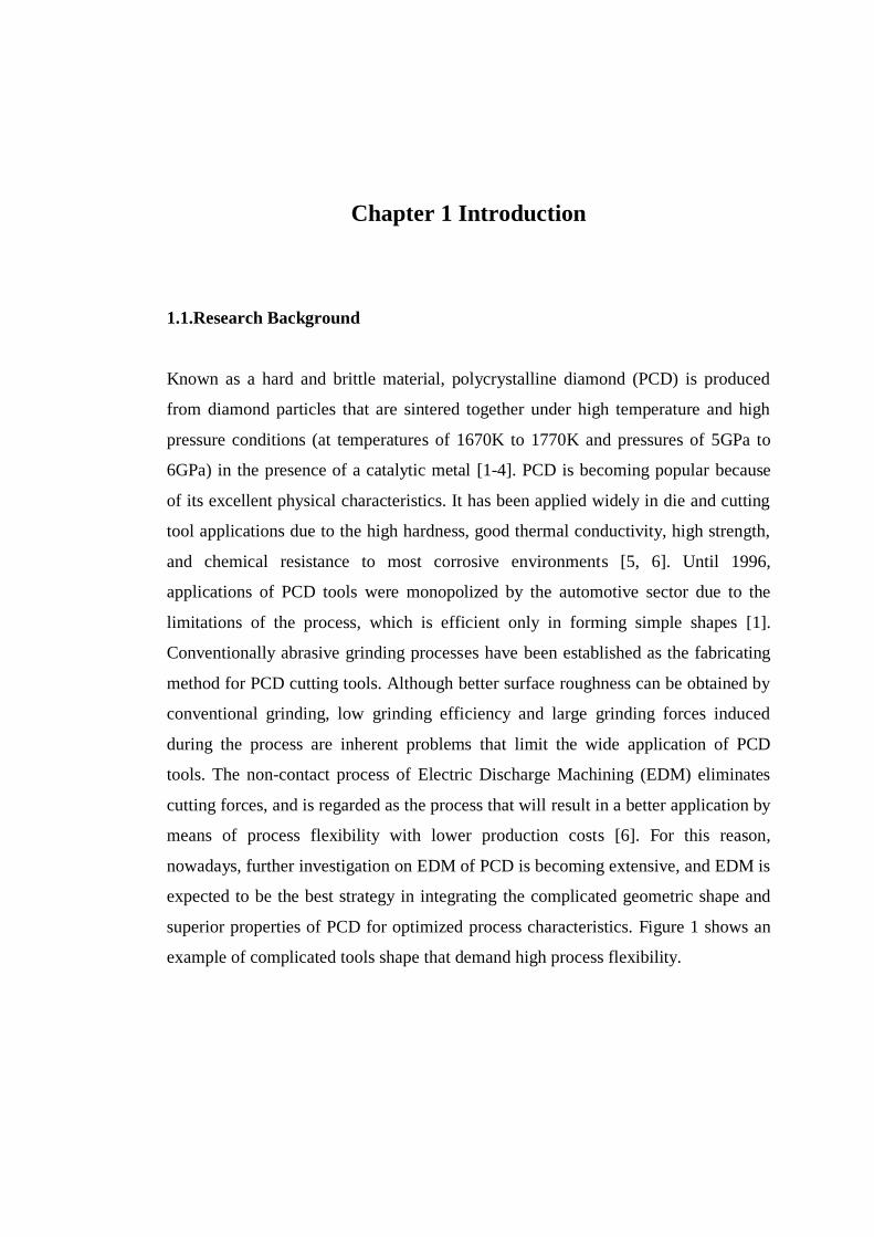
superior properties of PCD for optimized process characteristics. Figure 1 shows an
example of complicated tools shape that demand high process flexibility.
2
Chapter 1. Introduction
Figure 1: Example of special geometry drill-bit commercially available in
machining of fibre reinforced plastic material [7]
However, the EDM plasma with the temperature of up to 12000K in the EDM
process will cause damage to the machined surface [1]. Erasmus et al. [8] reported
that the PCD material would be subjected to reduction in compression stress when it
was repeatedly annealed to about 1070K. This might due to the graphitization
process catalysed by the cobalt (and typically has an onset temperature of around
1020K) [8]. The effect is expected to be more dominant for the EDMed surface,
since the temperature is comparatively much higher than the annealing temperature.
The damaged surface or surface integrity associated with the thermal effect include
graphitization and residual stress. This surface damage is usually correlated with the
zone termed the Heat Affected Zone (HAZ). In order to achieve better performance,
surface damage or defects should be controlled. Surface defects will induce stress
concentration that is also considered a weak spot for crack propagation. Removing
the damaged surface by grinding is not the best solution, especially when the surface
geometry is complex.
The available research includes the strategies on how to overcome the major
drawback in EDM, which is low production rate, and high surface roughness.
However, the PCD industries, especially in cutting tool production, should not only
consider the economic aspect, but also need to place emphasis on the quality aspect
of the product. The primary concern is that there is insufficient data on the surface
quality or surface integrity relating to the application performance of the tools. With
3
Chapter 1. Introduction
emphasis on the cutting tool product, this study is focused on the analysis of the
Polycrystalline Diamond (PCD) surface damage caused in the fabrication process,
specifically in the Electrical Discharge Grinding (EDG) process, and its optimization
strategies.
1.2. Objectives and Research Questions
Since its development, PCD has been applied in the aerospace, automotive, wood
and mining industries as cutting tools due to its outstanding cutting performance.
Because of the ultra-hardness and low electric conductivity, PCD tools are very
difficult to fabricate. The high costs caused by low machining efficiency have
seriously hindered its widespread application in industry.
Although PCD tools are superior in toughness (chipping resistance), a 300% to 500%
scatter in tool life has been reported in the automotive industries [9]. Indeed,
unexplained breakages of PCD tools used for similar applications are also common
[2, 9]. In addition to the direct cost of the tools, indirect costs are caused by the large
amount of time needed to replace failed tools and set up new ones on each shift each
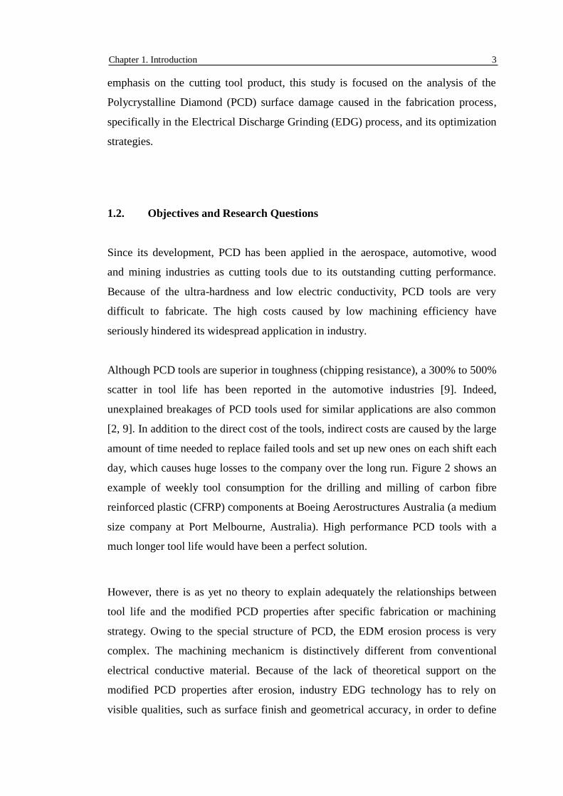
day, which causes huge losses to the company over the long run. Figure 2 shows an
example of weekly tool consumption for the drilling and milling of carbon fibre
reinforced plastic (CFRP) components at Boeing Aerostructures Australia (a medium
size company at Port Melbourne, Australia). High performance PCD tools with a
much longer tool life would have been a perfect solution.
However, there is as yet no theory to explain adequately the relationships between
tool life and the modified PCD properties after specific fabrication or machining
strategy. Owing to the special structure of PCD, the EDM erosion process is very
complex. The machining mechanicm is distinctively different from conventional
electrical conductive material. Because of the lack of theoretical support on the
modified PCD properties after erosion, industry EDG technology has to rely on
visible qualities, such as surface finish and geometrical accuracy, in order to define

4
Chapter 1. Introduction
the quality of the PCD tools. In fact, the author found that the other factors, such as
residual stress and graphitization significantly altered the PCD tool life, although
similar visible quality is achieved.
Figure 2: Weekly tool usage in Boeing Aerostructures Australia
As an attempt to resolve the issues, the following research objectives are defined:
a. To develop a new methodology to identify HAZ.
b. To find the best method to quantify the residual stress on PCD.
c. To investigate the effects of plasma temperature generated by electrical
sparks on PCD tool life.
d. To optimize the EDG parameters (electrode polarity, wheel rotation direction,
pulse on-time, pulse off-time, sparking voltage, and finishing in-feed) to
improve PCD tool performance.
The key research questions are:
a. How to determine the HAZ in PCD?
b. What are the structural differences between PCD tools manufactured with
different EDG processes?
c. What are the differences in residual stress between PCD tools manufactured
with EDG and conventional grinding processes?
5
Chapter 1. Introduction
d. What is the relationship between the plasma temperature in the EDG process
and PCD tool quality (tool life)?
e. How will the machining parameters (electrode polarity, wheel rotation
direction, pulse on-time, pulse off-time, sparking voltage, and finishing in-
feed) affect the wear behaviour of PCD tools?
1.3. Scope of the Investigation
The scope of this study is as follows:
a. The research includes both theoretical and experimental knowledge analysis.
b. PCD samples with cobalt binder and different particle sizes will be used in
this investigation.
c. Finishing processes are limited to conventional grinding and EDG.
d. CNC cutting tests will be conducted to prove and validate theoretical
findings.

6
Chapter 1. Introduction
1.4. Challenges in PCD Tools Fabrication
PCD is commonly produced in a thin layer of 0.5mm to 0.7mm thickness on a
supporting layer of tungsten carbide (WC). PCD tools are usually fabricated in three
steps:
a. Cut PCD blanks into small inserts;
b. Braze the inserts on a carbide substrate;
c. Machine and sharp the cutting edges into the required dimension and surface
finish.
Figure 3 shows an example of PCD tools for the milling process.
Figure 3: PCD tool.
The research was begun with the observation of the PCD tools‘ surface quality after
erosion. Several issues that were assumed as thermal damage indications caused by
the process were highlighted. This included the formation of cutting edge undercut
and some cosmetic aspects at the WC-PCD interface. However, whether the
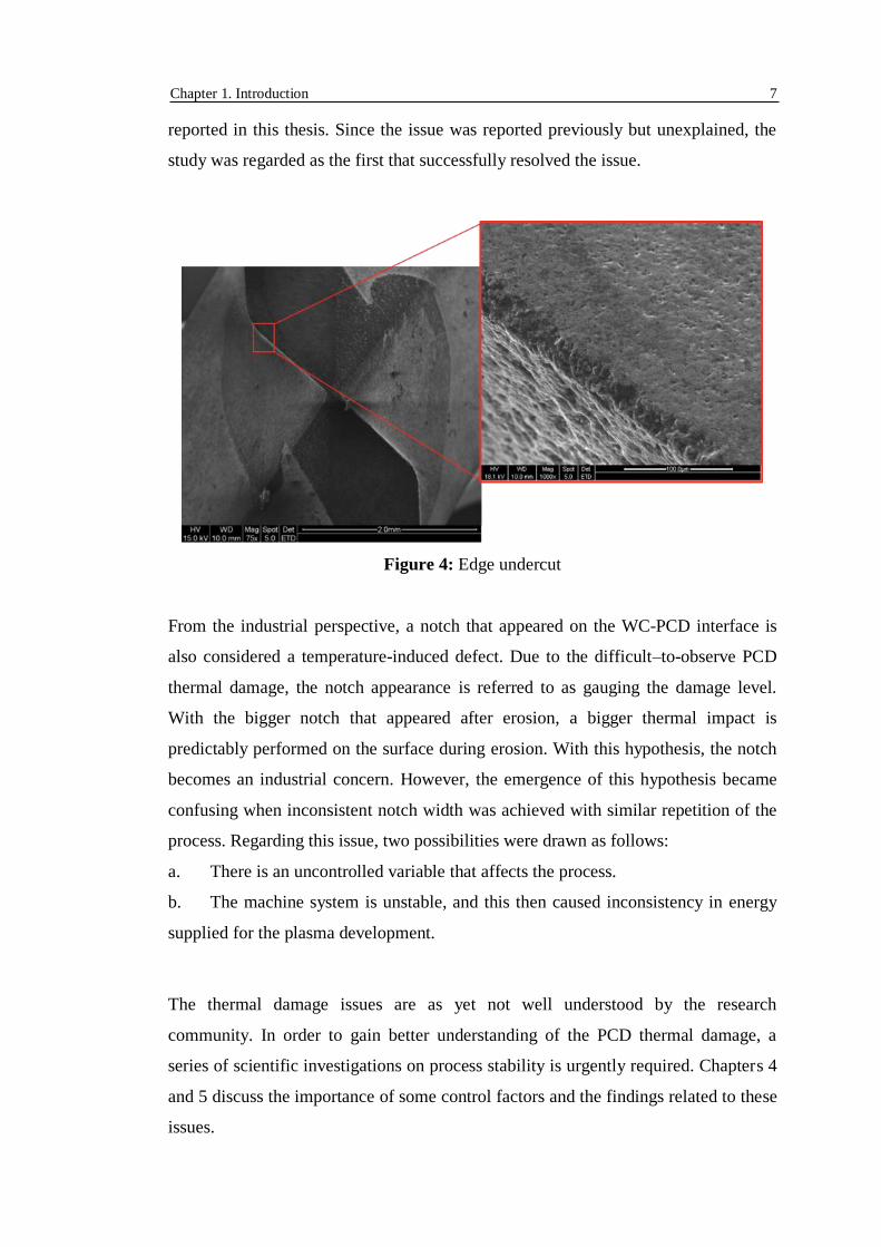
phenomena are the real implications of thermal damage was in question. Figure 4
shows the example of edge undercut mentioned. Initially, it was inferred that the
formation of edge undercut happened due to the excessive tensile stress generated on
the tip. However, the inference was incorrect and the exact reasons have been
7
Chapter 1. Introduction
reported in this thesis. Since the issue was reported previously but unexplained, the
study was regarded as the first that successfully resolved the issue.
Figure 4: Edge undercut
From the industrial perspective, a notch that appeared on the WC-PCD interface is
also considered a temperature-induced defect. Due to the difficult–to-observe PCD
thermal damage, the notch appearance is referred to as gauging the damage level.
With the bigger notch that appeared after erosion, a bigger thermal impact is
predictably performed on the surface during erosion. With this hypothesis, the notch
becomes an industrial concern. However, the emergence of this hypothesis became
confusing when inconsistent notch width was achieved with similar repetition of the
process. Regarding this issue, two possibilities were drawn as follows:
a. There is an uncontrolled variable that affects the process.
b. The machine system is unstable, and this then caused inconsistency in energy
supplied for the plasma development.
The thermal damage issues are as yet not well understood by the research
community. In order to gain better understanding of the PCD thermal damage, a
series of scientific investigations on process stability is urgently required. Chapters 4
and 5 discuss the importance of some control factors and the findings related to these
issues.
8
Chapter 1. Introduction
1.5. Research Methodology
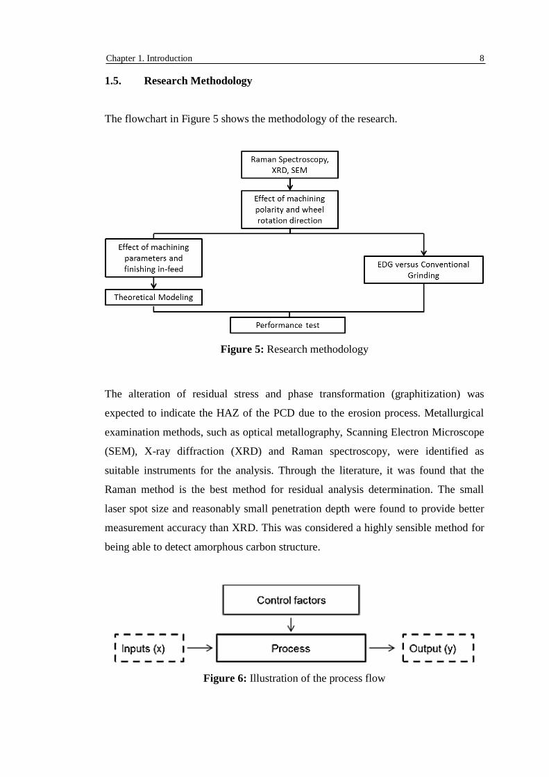
The flowchart in Figure 5 shows the methodology of the research.
Figure 5: Research methodology
The alteration of residual stress and phase transformation (graphitization) was
expected to indicate the HAZ of the PCD due to the erosion process. Metallurgical
examination methods, such as optical metallography, Scanning Electron Microscope
(SEM), X-ray diffraction (XRD) and Raman spectroscopy, were identified as
suitable instruments for the analysis. Through the literature, it was found that the
Raman method is the best method for residual analysis determination. The small
laser spot size and reasonably small penetration depth were found to provide better
measurement accuracy than XRD. This was considered a highly sensible method for
being able to detect amorphous carbon structure.
Figure 6: Illustration of the process flow
9
Chapter 1. Introduction
Determination of the control factors is a vital procedure for ensuring good
repeatability of the process and avoiding obstruction or interference of external
elements with the results obtained. Focusing on the surface quality and the cutting
edge sharpness, the effects of tool polarity and wheel rotation direction were
determined. The best strategies were then taken as the standard in the succeeding
investigation.
As the next step, the PCD-eroded surface quality was evaluated. Specimens that were
prepared by EDG with different machining parameters were analysed. With the aid
of the morphological findings, different PCD erosion mechanisms were discussed. A
comprehensive discussion was undertaken and the theoretical modelling of the
process was obtained. The structural differences between PCD manufactured with
EDG and conventional grinding were also compared. The performance test was
conducted at the end of the methodology as a process evaluation.
Overall, the research seeks to better understand the PCD surface thermal damage
caused by the EDG plasma and its influence on tool life. With this fundamental
understanding, better process optimization and better PCD tools utilization can be
expected.

Chapter 2 Literature Review
2.1. Introduction
The applications of PCD tools include the shaping of various materials, such as
aluminium alloy used in the automotive industries, and wood, rock and rubber [1, 3,
10-13]. Due to PCD‘s excellent properties, this tool material is also regarded as the
best candidate for machining exotic materials for the aerospace industries [14]. The
significant hardness and excellent thermal conductivity of PCD, of up to 920 W/mK,
makes it the most promising tool material for machining titanium [5]. In addition,
several studies demonstrate the use of PCD in micro-machining glass and other
micro optical-related devices made from tungsten carbide, electro-less plated nickel
and silicon [15, 16]. In Printed Circuit Board (PCB) industries, PCD has also been
used in the cutting tools with special blade configurations [2].
However, the outstanding mechanical, electrical and thermal properties of this
material have a negative influence in that uneconomical and inefficient
manufacturing processes often result [17, 18]. Low G ratios, high cutting force and
high wheel cost pose the main challenges to conventional grinding production of
PCD parts [17]. Similarly, for lapping processes, low efficiency, low removal rate,
high cost and poor consistency are the major problems [17, 19, 20]. Experiments
show that the G-ratio of conventional grinding of PCD tools is between 0.015 and
0.025 and MRR is between 0.226mm3/min and 0.886mm
3/min, depending on
different grind size and structures [21]. Another problem with conventional grinding
is the possibility of micro-cracks due to the high cutting force [21].
Brecher et al. [22] and Wang [23] used laser ablation, and achieved equivalent
surface quality as abrasive grinding. However, unless ultra-short laser pulses of
picoseconds were applied, which would result in unacceptably low MRR, a
11
Chapter 2. Literature Review
conventional abrasive grinding process has to be followed in order to remove the
severe heat affected zone [22]. In 2013, Qinjian et al. [24] developed another type of
hybrid method by combining electrical discharge machining and ultrasonic-assisted
mechanical grinding, but it was found that the hybrid method had limited impact on
MRR. Likewise, Iwai et al. [25] developed an abrasive grinding-assisted EDM by
using a metal-bounded diamond wheel for machining EC-PCD, but no obvious
improvement in the grinding ratio was achieved in grinding conventional PCD
material. For these reasons the EDM process is considered a good alternative for
machining PCD due to its non-contact nature.
EDM is a non-conventional material removal process that uses thermal energy to
melt or vaporize the work piece using high temperature sparks between the work
piece and an electrode. EDM can be used for all conductive materials, regardless of
their hardness and other mechanical properties, and is particularly good for fragile
work pieces [26]. This chapter reviews the current achievements and findings of the
EDM process of PCD.
2.2. PCD EDM Process
Early attempts to machine the diamond by EDM began in 1960. Heerschap et al. [27]
revealed that non-conductive diamond could be machined using EDM by
implementing a graphite coating on the diamond work piece. This is similar to the
concept of ―assisted electrode‖ used on EDM of insulated ceramics [28, 29]. To form
the conductive coating of graphite, the diamond was heated up by non-oxidising
flame to a temperature higher than its graphitization temperature [27, 30]. This was
to ensure the conversion of diamond into graphite specifically on the work piece
surface in order to provide a conductor path for spark initiation. The conductivity of
the graphite enabled initial sparking and the erosion process was caused to the
diamond-graphite conversion so that the process is self-sustaining. Hence, newly
formed graphite was obtained on the eroded surface, providing connection to the
current source [27, 30]. Figure 7 illustrates the aforementioned erosion concept.

12
Chapter 2. Literature Review
Figure 7: Graphite Coating Method
The emergence of PCD resolved the issues of non-conductivity of diamond. The
presence of up to 15% by weight of metallic cobalt in the PCD composition makes it
possible to machine PCD using EDM [6, 31-33]. Research on PCD EDM may be
divided into Die/Sink EDM, EDG and Electrical Discharge Wire Machining
(EDWM). Although they posit the same concept, EDG and EDWM vary
significantly in machining parameters. Instead of static electrodes typically used in
Die/Sink EDM, a rotating electrode wheel is used in EDG. This improves the
flushing efficiency, since the rotating wheel electrode effectively drags dielectric into
the gap. It thus yields better in-material removal rate, tool wear ratio and surface
roughness [34-37].
2.2.1. EDM Polarity
Several studies show that a lesser electrode wear ratio was obtained when positive
polarity of the tool electrode was used during EDM of PCD [6, 38]. Carbon plating
of the positive electrode (which is the electrode in this case) was believed to be the
reason for the reduction of electrode wear when this method is used [6, 39]. The

13
Chapter 2. Literature Review
transformation of diamond into other forms of carbon occurs during the EDM
sparking process. The result from the conversion process is the formation carbon
ions, which are then involved in the positive electrode plating operation. This heat-
resolved carbon acts as a shield that protects the electrode from wear [6].
Furthermore, the deposited carbon is also reported to come from the dielectric
medium when hydrocarbon dielectric was used [40].
However, the adhesion also had a negative impact on process precision. Wang et al.
[6] revealed that the formation of carbon adhesion (graphite and amorphous carbon)
on the silver-tungsten alloy electrode rod led to increases in the effective electrode
size. It thus produced a hole with a size bigger than the required dimension.
Particularly in micro-hole machining, increase in the electrode size due to plating
phenomena will significantly affect process precision. The comparison of the shape
of electrodes after EDM with different polarity is shown in Figure 8.
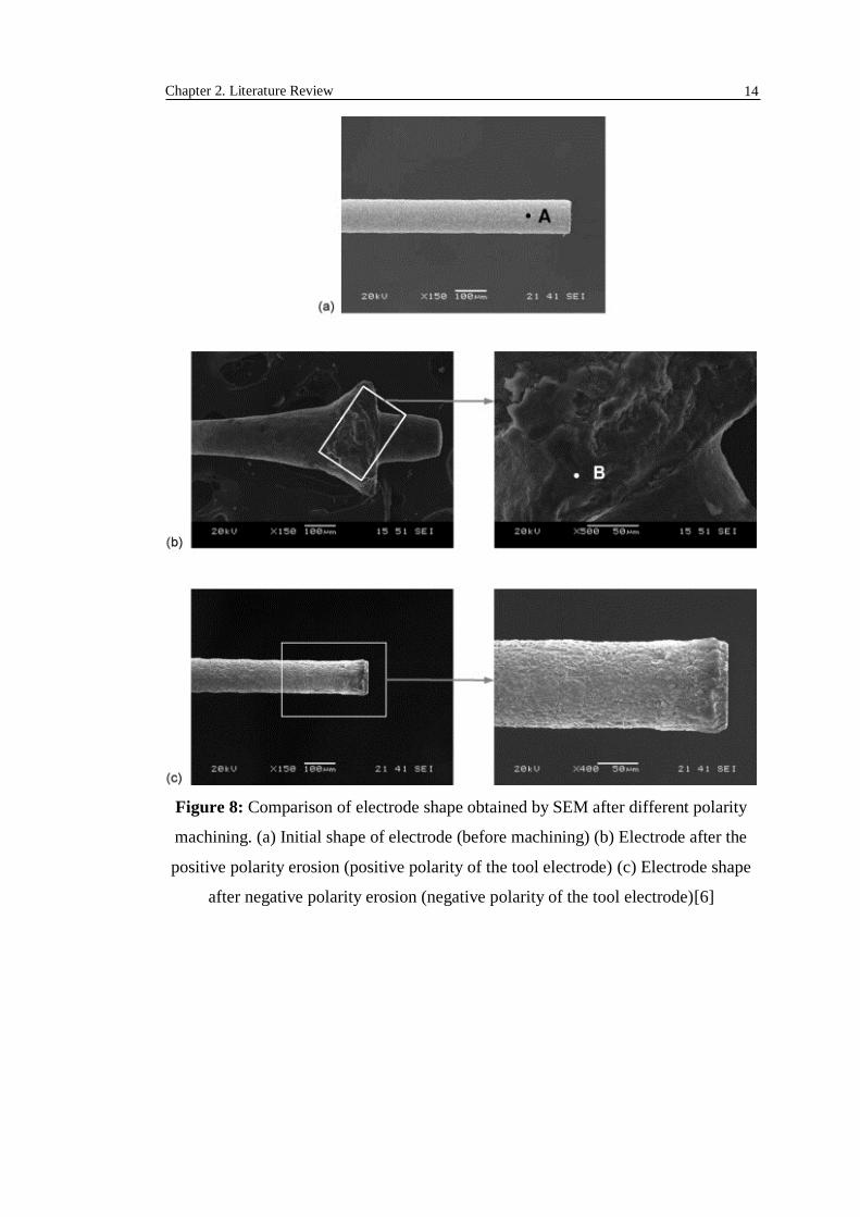
14
Chapter 2. Literature Review
Figure 8: Comparison of electrode shape obtained by SEM after different polarity
machining. (a) Initial shape of electrode (before machining) (b) Electrode after the
positive polarity erosion (positive polarity of the tool electrode) (c) Electrode shape
after negative polarity erosion (negative polarity of the tool electrode)[6]

15
Chapter 2. Literature Review
2.2.2. Material Removal Rate
Considering the thermal conductivity, specific heat, and melting point of materials,
Wang et al. [6] quantified the degree of difficulty for EDM of several materials. The
degree of difficulty for a material to be eroded can be calculated using the following
formula:
Cm = KCTm2 (2.1)
where Cm is the erosion resistance index (ERI) (1012
J2
/ m s kg) and K, C and Tm are
the thermal conductivity expressed in W/(mK), specific heat is expressed in J/(kg K),
and melting point is expressed in K, respectively. As shown in Table 1, in
comparison to the ERI of tungsten, copper and steel, the highest ERI was attributed
to PCD, indicating that PCD is the hardest material to be eroded by EDM.
Table 1: Erosion resistance index (ERI) of materials [6]
Material Erosion resistance index (1012
J2
/ m s kg)
Tungsten 2.99
Copper 2.79
Steel 0.230
PCD 4
It is well understood that the smaller PCD grain size will give better MRR, because it
has higher electrical conductivity than PCD with bigger grains. This is due to the fact
that PCD with smaller grain size has a higher proportion of cobalt content than is the
case with bigger grain size PCD. Since cobalt is a highly conductive material and
diamond is non-conductive, the electrical conductivity of smaller grain PCD is
higher.
16
Chapter 2. Literature Review
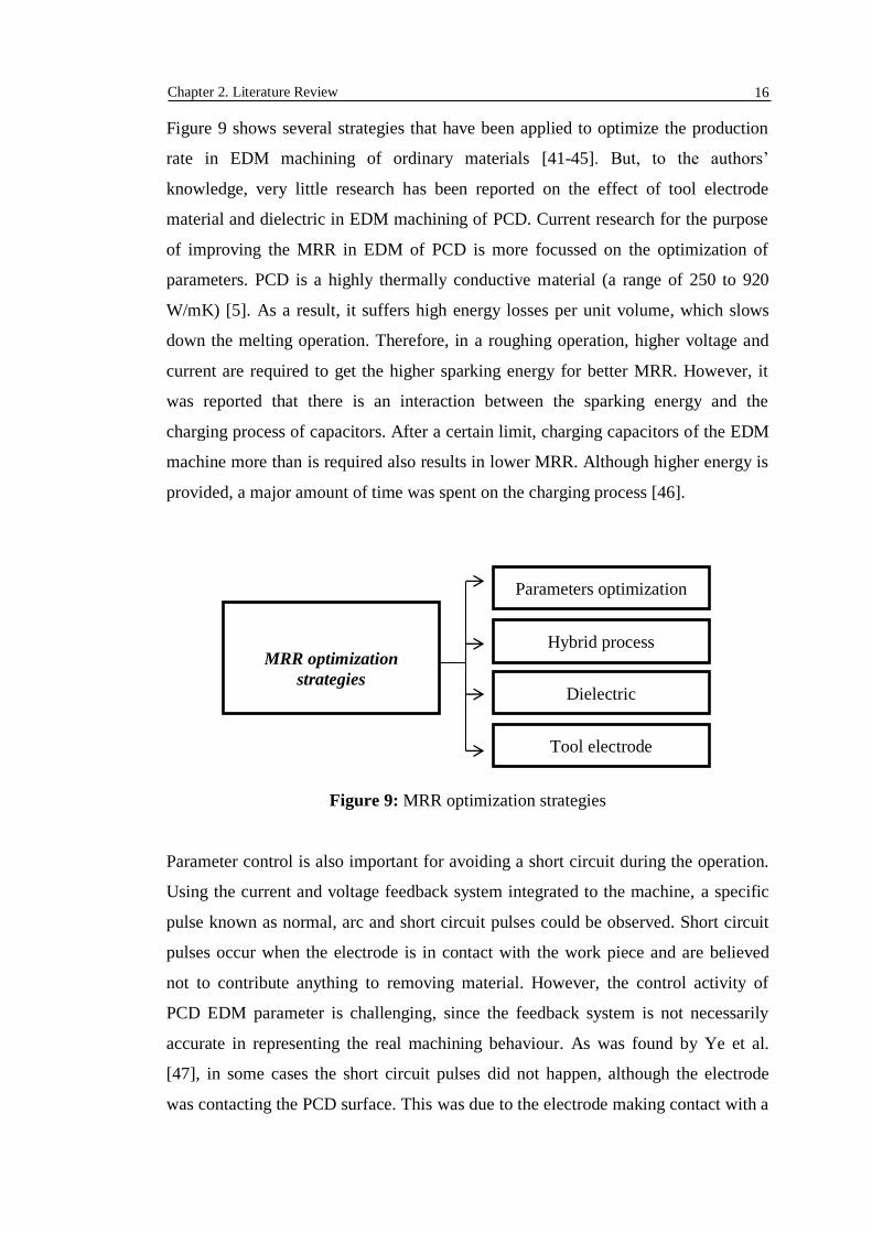
Figure 9 shows several strategies that have been applied to optimize the production
rate in EDM machining of ordinary materials [41-45]. But, to the authors‘
knowledge, very little research has been reported on the effect of tool electrode
material and dielectric in EDM machining of PCD. Current research for the purpose
of improving the MRR in EDM of PCD is more focussed on the optimization of
parameters. PCD is a highly thermally conductive material (a range of 250 to 920
W/mK) [5]. As a result, it suffers high energy losses per unit volume, which slows
down the melting operation. Therefore, in a roughing operation, higher voltage and
current are required to get the higher sparking energy for better MRR. However, it
was reported that there is an interaction between the sparking energy and the
charging process of capacitors. After a certain limit, charging capacitors of the EDM
machine more than is required also results in lower MRR. Although higher energy is
provided, a major amount of time was spent on the charging process [46].
Figure 9: MRR optimization strategies
Parameter control is also important for avoiding a short circuit during the operation.
Using the current and voltage feedback system integrated to the machine, a specific
pulse known as normal, arc and short circuit pulses could be observed. Short circuit
pulses occur when the electrode is in contact with the work piece and are believed
not to contribute anything to removing material. However, the control activity of
PCD EDM parameter is challenging, since the feedback system is not necessarily
accurate in representing the real machining behaviour. As was found by Ye et al.
[47], in some cases the short circuit pulses did not happen, although the electrode
was contacting the PCD surface. This was due to the electrode making contact with a
MRR optimization
strategies
Tool electrode
Parameters optimization
Dielectric
Hybrid process
17
Chapter 2. Literature Review
non-conductive diamond particle that protruded from the PCD surface and the
sparking still being between the cobalt and the electrode.
2.2.3. Surface Roughness and Morphology
Surface roughness is an important factor that affects the performance of cutting tools,
particularly in high precision machining [5, 48]. Due to the extremely high hardness
of PCD, together with high chemical stability, mechanical processing does not
appear to be the best machining strategy for producing a very fine surface while
considering the production cost [5].
In the roughing operation of PCD EDM, granularity of the surface results when
individual diamond grains drop out of the surface, which makes the roughness value
proportional to the grain size [1]. Hence, finer grain size is to be preferred when a
better surface finish is a priority. However, in some tool applications, specifically in
machining metal matrix composite (MMC) materials, bigger grain PCD is
preferential. The investigation into the performance of PCD tools in machining of
MMCs showed that better tool wear performance was achieved by PCD with bigger
grains [49-51]. Although better in surface finish, a high percentage of cobalt in small
PCD grain structure is also believed to be involved in weakening the structure, due to
its affinity for carbon and its catalytic action in changing diamond to other forms of
carbon at high temperatures [52]. For this reason, the investigation of surface
roughness obtained by the fabrication process, especially for big PCD grain (10µm
grain size and above), is crucial for the development of high performance tools.
Olsen et al. [32] believed that, during the sparking process, some diamond grains
were lost as a result of the highly conductive cobalt network being preferentially
eroded [31, 32]. For this reason, sparked PCD surfaces were generally of lower
quality than conductive Chemical Vaporized Deposition (CVD) diamond film, so-
called CVDITE CDE, even when fine diamond is used (2µm) [31].Unlike PCD, in
CVDITE CDE film production, the conductivity of diamond grains is increased by
increasing the electrical conductivity of the diamond crystal itself through boron

18
Chapter 2. Literature Review
doping [32]. Therefore, the spark will not only initiate on the grain boundary but can
also happen on the grain surface. This led to the EDM of CVDITE CDE process
cutting through the diamond crystal and not detaching the grains as a reason for finer
surface value. [31]. To better understand the difference in mechanism, PCD and
CVDITE CDE film material are compared in Table 2. It was believed that the major
factor causing selective erosion of the PCD is the low electrical conductivity of
diamond in contrast to the highly conductive cobalt path at the grain boundaries.
Table 2: Comparison between PCD and CVDITE CDE material
PCD material
Conductive CVD
(CVDITE CDE)
material
Thermal
conductivity
Around 459 W/mK (for 10µm
grains)[53] Up to 2200 W/mK[32]
Compositions Consists of cobalt binder and
diamond grains
Consists of no metallic
second phase [32]
Grains structure
Diamond might comprising both
lamellar and fine grains, depends on
the production method and starting
materials [54].
Comprising only
columnar/ lamellar
diamond grains [32].
Specific
resistance 1.4×10
-4Ωm[53] 0.4~1 x10
-3 Ωm [55]
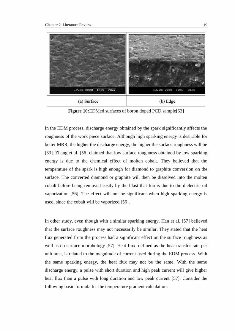
This principle has also been proved by Suzuki et al. [53]. A new type of PCD was
developed by following the same concept as conductive CVDITE CDE. The boron
atoms were incorporated into the diamond lattice in order to increase electrical
conductivity [32, 53]. As a result, better surface finish than the standard PCD was
achieved after the WEDM process. Interestingly, observation on the new PCD
developed showed that the grain was flattened by the electro-discharge process
(Figure 10). Better oxidation resistance might also be the other factor contributing to
the lower surface roughness of the boron-doped PCD while EDMed in water
dielectric. By oxidation analysis of CVD (CVDITE CDE), it was shown that better
oxidation resistance is obtained when the diamond is doped with boron [55].
19
Chapter 2. Literature Review
Figure 10:EDMed surfaces of boron doped PCD sample[53]
In the EDM process, discharge energy obtained by the spark significantly affects the
roughness of the work piece surface. Although high sparking energy is desirable for
better MRR, the higher the discharge energy, the higher the surface roughness will be
[33]. Zhang et al. [56] claimed that low surface roughness obtained by low sparking
energy is due to the chemical effect of molten cobalt. They believed that the
temperature of the spark is high enough for diamond to graphite conversion on the
surface. The converted diamond or graphite will then be dissolved into the molten
cobalt before being removed easily by the blast that forms due to the dielectric oil
vaporization [56]. The effect will not be significant when high sparking energy is
used, since the cobalt will be vaporized [56].
In other study, even though with a similar sparking energy, Han et al. [57] believed
that the surface roughness may not necessarily be similar. They stated that the heat
flux generated from the process had a significant effect on the surface roughness as
well as on surface morphology [57]. Heat flux, defined as the heat transfer rate per
unit area, is related to the magnitude of current used during the EDM process. With
the same sparking energy, the heat flux may not be the same. With the same
discharge energy, a pulse with short duration and high peak current will give higher
heat flux than a pulse with long duration and low peak current [57]. Consider the
following basic formula for the temperature gradient calculation:
20
Chapter 2. Literature Review
q= -K ΔT (2.2)
where ΔT, q and K are the temperature difference, heat flux and material
conductivity, respectively. Rearrange equation 2.2 so that:
T2 - T1= - q/K (2.3)
Since the heat flux is a vectorial quantity, T2 should be defined as the temperature on
deeper surface and T1 is the temperature of the surface that is exposed to the spark.
Higher heat flux, defined as the higher heat rate per unit area, will reduce the chance
of heat losses due to the conduction on the surface, thus creating deeper craters.
Little research has been done regarding the effect of dielectric in the machining of
PCD materials. WEDM of PCD in oil can result in better surface quality than
deionized water [53]. It was also reported that implementing WEDM of PCD in a
water bath would increase the selective erosion on the cobalt region, since the cobalt
has a much higher electrochemical equivalence than the other elements in PCD [58,
59]. Furthermore, the oxygen content in water also results in the oxidation of the
PCD machined surface [55]. Wu et al. have shown the increase in oxygen content
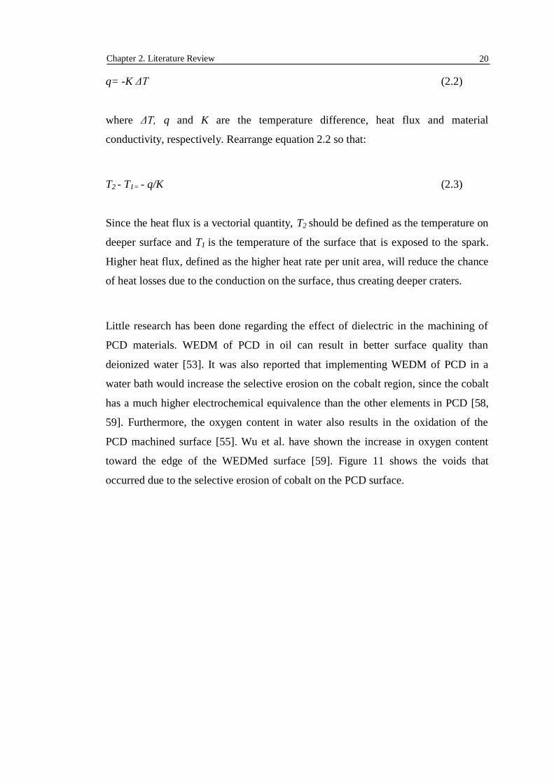
toward the edge of the WEDMed surface [59]. Figure 11 shows the voids that
occurred due to the selective erosion of cobalt on the PCD surface.
21
Chapter 2. Literature Review
Figure 11: Void due to selective erosion [59]
2.2.4. Challenges on Cutting of Laminar Discs
The laminar disc blanks are made from PCD on a carbide substrate. Although the
carbide substrate provides the PCD tools with sufficient toughness [60], EDM of this
laminar structure is a challenge, since the layers are made of materials with
dissimilar properties [58, 61]. Preferential erosion of the carbide occurs at the PCD-
carbide interface and this not only causes a notch to form but also increases residual
stress in this area [1]. The notch is believed to be more dominant when the bigger
grain structure is used [1]. An analysis was conducted by Cao et al. [17] in an
attempt to minimize the notch depth that was categorized as the most serious PCD
surface defect caused by EDM. Through parameter optimization, they successfully
reduced the notch depth on the diamond-WC interface to only 0.03mm [17].
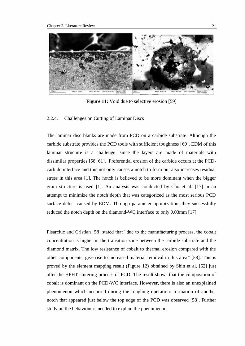
Pisarciuc and Cristian [58] stated that ―due to the manufacturing process, the cobalt
concentration is higher in the transition zone between the carbide substrate and the
diamond matrix. The low resistance of cobalt to thermal erosion compared with the
other components, give rise to increased material removal in this area‖ [58]. This is
proved by the element mapping result (Figure 12) obtained by Shin et al. [62] just
after the HPHT sintering process of PCD. The result shows that the composition of
cobalt is dominant on the PCD-WC interface. However, there is also an unexplained
phenomenon which occurred during the roughing operation: formation of another
notch that appeared just below the top edge of the PCD was observed [58]. Further
study on the behaviour is needed to explain the phenomenon.
22
Chapter 2. Literature Review
Figure 12: Element Mapping of (a) C, (b) Co, (c) Ta and (d) W [62]
2.2.5. Heat Affected Zone (HAZ)
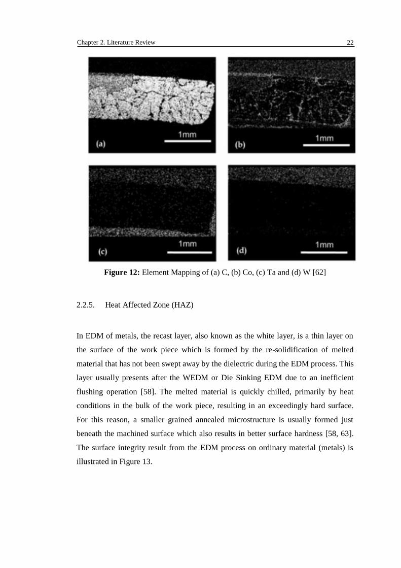
In EDM of metals, the recast layer, also known as the white layer, is a thin layer on
the surface of the work piece which is formed by the re-solidification of melted
material that has not been swept away by the dielectric during the EDM process. This
layer usually presents after the WEDM or Die Sinking EDM due to an inefficient
flushing operation [58]. The melted material is quickly chilled, primarily by heat
conditions in the bulk of the work piece, resulting in an exceedingly hard surface.
For this reason, a smaller grained annealed microstructure is usually formed just
beneath the machined surface which also results in better surface hardness [58, 63].
The surface integrity result from the EDM process on ordinary material (metals) is
illustrated in Figure 13.

23
Chapter 2. Literature Review
Figure 13: Heat affected zone of EDMed surface [58]
The heat affected zone (HAZ) when machining a metal is the zone that is subjected
to very high temperatures, though not high enough to be melted, but which promotes
some microstructure changes [43, 58, 64]. It will generally extend to a depth of a few
microns beneath the machined surface. Research has shown that the surface damage
due to the heat of plasma appeared up to 0.05mm in depth [31]. The depth is
dependent on the temperature gradient profile, which is affected by the electrode
materials, dielectric and machining conditions [43]. Although a recast layer may not
be generated in the EDG of PCD, there will generally be a HAZ, which is largely
unavoidable when dealing with thermal processing. This HAZ is also generally
called the modified zone or affected layer by some researchers when dealing with
PCD [65, 66].
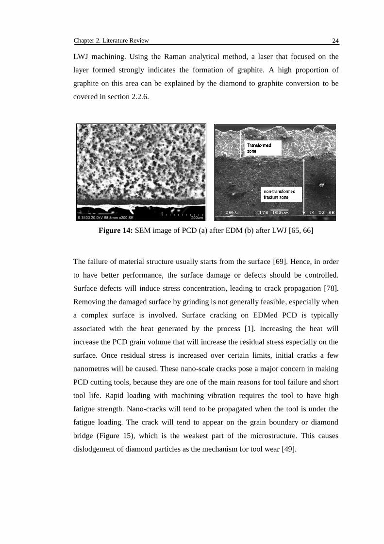
Metallurgical examination of the surfaces using various techniques such as optical
metallography, Scanning Electron Microscope (SEM), X-ray diffraction (XRD) and
Raman spectroscopy has been undertaken by many researchers to study the
behaviour of material due to thermal stress [65-77]. The affected layer with a
thickness more than 70µm has been observed on the PCD surface after EDM with a
roughing condition [65] (Figure 14a). The thickness of this layer is also believed to
significantly affect PCD tool life. However, detailed explanation of the structural
properties of this layer has remained unknown. As shown in Figure 14b, nearly the
same layer was also observed by Kalyanasundram et al. on the PCD sample after
24
Chapter 2. Literature Review
LWJ machining. Using the Raman analytical method, a laser that focused on the
layer formed strongly indicates the formation of graphite. A high proportion of
graphite on this area can be explained by the diamond to graphite conversion to be
covered in section 2.2.6.
Figure 14: SEM image of PCD (a) after EDM (b) after LWJ [65, 66]
The failure of material structure usually starts from the surface [69]. Hence, in order
to have better performance, the surface damage or defects should be controlled.
Surface defects will induce stress concentration, leading to crack propagation [78].
Removing the damaged surface by grinding is not generally feasible, especially when
a complex surface is involved. Surface cracking on EDMed PCD is typically
associated with the heat generated by the process [1]. Increasing the heat will
increase the PCD grain volume that will increase the residual stress especially on the
surface. Once residual stress is increased over certain limits, initial cracks a few
nanometres will be caused. These nano-scale cracks pose a major concern in making
PCD cutting tools, because they are one of the main reasons for tool failure and short
tool life. Rapid loading with machining vibration requires the tool to have high
fatigue strength. Nano-cracks will tend to be propagated when the tool is under the
fatigue loading. The crack will tend to appear on the grain boundary or diamond
bridge (Figure 15), which is the weakest part of the microstructure. This causes
dislodgement of diamond particles as the mechanism for tool wear [49].
References
[1] T. B. Thoe, D. K. Aspinwall, M. L. H. Wise, and I. A. Oxley,
"Polycrystalline diamond edge quality and and surface integrity following
electrical discharge grinding," Journal of Materials Processing Technology,
vol. 56, pp. 773-785, 1996.
[2] P.-L. Tso and Y.-G. Liu, "Study on PCD machining," International Journal
of Machine Tools and Manufacture, vol. 42, pp. 331-334, 2002.
[3] L. Jaworska, "Diamond-Ceramic Bonding Phase Composites for Application
in Cutting Tools," Ceramic Materials, vol. 63, pp. 131-137, 2011.
[4] J. Yan, Y. Murakami, and J. P. Davim, "Tool Design, Tool Wear and Tool
Life," Machining Dynamics, pp. 117-149, 2009.
[5] Y. Chen, L. C. Zhang, J. A. Arsecularatne, and C. Montross, "Polishing of
polycrystalline diamond by the technique of dynamic friction, part 1:
Prediction of the interface temperature rise," International Journal of
Machine Tools and Manufacture, vol. 46, pp. 580-587, 2006.
[6] D. Wang, W. S. Zhao, L. Gu, and X. M. Kang, "A study on micro-hole
machining of polycrystalline diamond by micro-electrical discharge
machining," Journal of Materials Processing Technology, vol. 211, pp. 3-11,
2011.
[7] V. Schulze, C. Becke, K. Weidenmann, and S. Dietrich, "Machining
strategies for hole making in composites with minimal workpiece damage by
directing the process forces inwards," Journal of Materials Processing
Technology, vol. 211, pp. 329-338, 2011.
[8] R. M. Erasmus, J. D. Comins, V. Mofokeng, and Z. Martin, "Application of
Raman spectroscopy to determine stress in polycrystalline diamond tools as a
function of tool geometry and temperature," Diamond and Related Materials,
vol. 20, pp. 907-911, 2011.
[9] V. P. Astakhov and A. Stanley, "Polycrystalline Diamond (PCD) Tool
Material: Emerging Applications, Problems, and Possible Solutions," in
Traditional Machining Processes, ed: Springer, 2015, pp. 1-32.
162
[10] M. H. Paul Harrison, Jozef Wendland, "Enhanced Cutting of Polycrytalline
Diamond with a Q-switched Diode Pumped Solid State Laser," 2005.
[11] Q. Bai, Y. Yao, and S. Chen, "Research and development of polycrystalline
diamond woodworking tools," International Journal of Refractory Metals
and Hard Materials, vol. 20, pp. 395-400, 2002.
[12] P. J. Heath, "Developments in applications of PCD tooling," Journal of
Materials Processing Technology, vol. 116, pp. 31-38, 2001.
[13] V. Mărăscu-klein, "The application of carbon materials in advanced
technologies."
[14] J. Mo, S. L. Ding, A. Mackie, M. Brandt, S. J. Sun, R. Hoseinnezhad, and R.
Webb, "Design of Exotic Materials Machining System," Advanced Materials
Research, vol. 633, pp. 36-46, 2013.
[15] T. Wada, T. Masaki, and D. W. Davis, "Development of micro grinding
process using micro EDM trued diamond tools," in ASPE Proceeding, Annual
Meeting, 2002, pp. 16-19.
[16] C. J. Morgan, R. R. Vallance, and E. R. Marsh, "Micro machining glass with
polycrystalline diamond tools shaped by micro electro discharge machining,"
Journal of Micromechanics and Microengineering, vol. 14, p. 1687, 2004.
[17] F. Cao and Q. Zhang, "Neural network modelling and parameters
optimization of increased explosive electrical discharge grinding (IEEDG)
process for large area polycrystalline diamond," Journal of Materials
Processing Technology, vol. 149, pp. 106-111, 2004.
[18] G. F. Zhang, B. Zhang, Z. H. Deng, and J. F. Chen, "An Experimental Study
on Laser Cutting Mechanisms of Polycrystalline Diamond Compacts," CIRP
Annals - Manufacturing Technology, vol. 56, pp. 201-204, 2007.
[19] M. Najafi-sani and P. A. Bex, "Shaping of bonded abrasive products," ed: EP
Patent 0,368,654, 1994.
[20] A. P. Malshe, B. S. Park, W. D. Brown, and H. A. Naseem, "A review of
techniques for polishing and planarizing chemically vapor-deposited (CVD)
diamond films and substrates," Diamond and Related Materials, vol. 8, pp.
1198-1213, 1999.
163
[21] Y.-K. Liu and P.-L. Tso, "The optimal diamond wheels for grinding diamond
tools," The International Journal of Advanced Manufacturing Technology,
vol. 22, pp. 396-400, 2003.
[22] C. Brecher, M. Emonts, J.-P. Hermani, and T. Storms, "Laser Roughing of
PCD," Physics Procedia, vol. 56, pp. 1107-1114, 2014.
[23] Q. Wu, J. Wang, and C. Huang, "Analysis of the machining performance and
surface integrity in laser milling of polycrystalline diamonds," Proceedings of
the Institution of Mechanical Engineers, Part B: Journal of Engineering
Manufacture, vol. 228, pp. 903-917, 2014.
[24] Z. Qinjian, Z. Luming, L. Jianyong, C. Yonglin, W. Heng, C. Yunan, S.
Haikuo, Y. Xiaoqing, and L. Minzhi, "Study on electrical discharge and
ultrasonic assisted mechanical combined machining of polycrystalline
diamond," Procedia CIRP, vol. 6, pp. 589-593, 2013.
[25] M. Iwai, S. Ninomiya, and K. Suzuki, "Effect of complex electrodischarge
grinding for electrically conductive PCD," Advanced Materials Research,
vol. 325, pp. 276-281, 2011.
[26] K. Ho and S. Newman, "State of the art electrical discharge machining
(EDM)," International Journal of Machine Tools and Manufacture, vol. 43,
pp. 1287-1300, 2003.
[27] C. M. Levitt, "Eroding of hard crystalline carbon," ed: Google Patents, 1960.
[28] N. Mohri, Y. Fukuzawa, T. Tani, N. Saito, and K. Furutani, "Assisting
electrode method for machining insulating ceramics," CIRP Annals-
Manufacturing Technology, vol. 45, pp. 201-204, 1996.
[29] T. Tani, Y. Fukuzawa, N. Mohri, N. Saito, and M. Okada, "Machining
phenomena in WEDM of insulating ceramics," Journal of Materials
Processing Technology, vol. 149, pp. 124-128, 2004.
[30] M. Kunieda, B. Lauwers, K. P. Rajurkar, and B. M. Schumacher, "Advancing
EDM through Fundamental Insight into the Process," CIRP Annals -
Manufacturing Technology, vol. 54, pp. 64-87, 2005.
[31] R. H. Olsen, D. K. Aspinwall, and R. C. Dewes, "Electrical discharge
machining of conductive CVD diamond tool blanks," Journal of Materials
Processing Technology, vol. 155–156, pp. 1227-1234, 2004.
164
[32] R. H. Olsen, R. C. Dewes, and D. K. Aspinwall, "Machining of electrically
conductive CVD diamond tool blanks using EDM," Journal of Materials
Processing Technology, vol. 149, pp. 627-632, 2004.
[33] J. M. Chris, R. R. Vallance, and R. M. Eric, "Micro machining glass with
polycrystalline diamond tools shaped by micro electro discharge machining,"
Journal of Micromechanics and Microengineering, vol. 14, p. 1687, 2004.
[34] S. S. Anand Pandey, "Current research trends in variants of Electrical
Discharge Machining: A review," International Journal of Engineering
Science and Technology, vol. Vol. 2(6), pp. 2172-2191, 2010.
[35] J. S. Soni, "Microanalysis of debris formed during rotary EDM of titanium
alloy (Ti 6A1 4V) and die steel (T 215 Cr12)," Wear, vol. 177, pp. 71-79,
1994.
[36] P. Koshy, V. K. Jain, and G. K. Lal, "Experimental investigations into
electrical discharge machining with a rotating disk electrode," Precision
Engineering, vol. 15, pp. 6-15, 1993.
[37] S. Singh and A. Bhardwaj, "Review to EDM by using water and powder-
mixed dielectric fluid," Journal of Minerals and Materials Characterization
and Engineering, vol. 10, p. 199, 2011.
[38] E. Uhlmann and M. Roehner, "Investigations on reduction of tool electrode
wear in micro-EDM using novel electrode materials," CIRP Journal of
Manufacturing Science and Technology, vol. 1, pp. 92-96, 2008.
[39] R. J. Weetnam, "The Characteristic of DC Arcd As Related to Electrical
Discharge Machining," Department of Mechanical Engineering,
Massachusetts Institute of Technology, 1968.
[40] D. A. Khan and M. HAMEEDULLAH, "Effect of tool polarity on the
Machining Characteristics in Electric Discharge Machining of Silver Steel
and Statistical Modelling of the Process," International Journal of
Engineering Science, vol. 3, 2011.
[41] H. Zarepour, A. F. Tehrani, D. Karimi, and S. Amini, "Statistical analysis on
electrode wear in EDM of tool steel DIN 1.2714 used in forging dies,"
Journal of Materials Processing Technology, vol. 187, pp. 711-714, 2007.
165
[42] M. Jeswani, "Effect of the addition of graphite powder to kerosene used as
the dielectric fluid in electrical discharge machining," Wear, vol. 70, pp. 133-
139, 1981.
[43] K. M. Shu and G. C. Tu, "Study of electrical discharge grinding using metal
matrix composite electrodes," International Journal of Machine Tools and
Manufacture, vol. 43, pp. 845-854, 2003.
[44] S. Singh, S. Maheshwari, and P. Pandey, "Some investigations into the
electric discharge machining of hardened tool steel using different electrode
materials," Journal of Materials Processing Technology, vol. 149, pp. 272-
277, 2004.
[45] V. K. Meena, "Optimization of EDM machining parameters using DMLS
electrode," Rapid Prototyping Journal, vol. 12, pp. 222-228, 2006.
[46] S. Kumar, R. Singh, T. P. Singh, and B. L. Sethi, "Surface modification by
electrical discharge machining: A review," Journal of Materials Processing
Technology, vol. 209, pp. 3675-3687, 2009.
[47] S. L. Ye, W. C. Pan, S. L. Ding, J. Mo, M. Brandt, and A. Mackie, "Electrical
Discharge Characteristics of Polycrystalline Diamonds," Advanced Materials
Research, vol. 426, pp. 44-47, 2012.
[48] B. Podgornik, S. Hogmark, and O. Sandberg, "Influence of surface roughness
and coating type on the galling properties of coated forming tool steel,"
Surface and Coatings Technology, vol. 184, pp. 338-348, 2004.
[49] J. A. Arsecularatne, L. C. Zhang, and C. Montross, "Wear and tool life of
tungsten carbide, PCBN and PCD cutting tools," International Journal of
Machine Tools and Manufacture, vol. 46, pp. 482-491, 2006.
[50] K. Weinert and W. König, "A Consideration of Tool Wear Mechanism when
Machining Metal Matrix Composites (MMC)," CIRP Annals - Manufacturing
Technology, vol. 42, pp. 95-98, 1993.
[51] R. T. Coelho, S. Yamada, D. K. Aspinwall, and M. L. H. Wise, "The
application of polycrystalline diamond (PCD) tool materials when drilling
and reaming aluminium based alloys including MMC," International Journal
of Machine Tools and Manufacture, vol. 35, pp. 761-774, 5// 1995.
166
[52] F. A. Almeida, A. J. S. Fernandes, F. J. Oliveira, and R. F. Silva, "Semi-
orthogonal turning of hardmetal with CVD diamond and PCD inserts at
different cutting angles," Vacuum, vol. 83, pp. 1218-1223, 2009.
[53] K. Suzuki, Y. Shiraishi, N. Nakajima, M. Iwai, S. Ninomiya, Y. Tanaka, and
T. Uematsu, "Development of new PCD made up of boron doped diamond
particles and its machinability by EDM," Advanced Materials Research, vol.
76, pp. 684-689, 2009.
[54] T. I. Hitoshi SUMIYA, "Microstructure and Mechanical Properties of High-
Hardness Nano-Polycrystalline Diamonds," SEI Technical Review pp. 85-91,
April 2008 2008
[55] A. Sharma, M. Iwai, K. Suzuki, and T. Uematsu, "Potential of electrically
conductive chemical vapor deposited diamond as an electrode for micro-
electrical discharge machining in oil and water," New Diamond and Frontier
Carbon Technology, vol. 15, pp. 181-194, 2005.
[56] Z. Zhang, H. Peng, and J. Yan, "Micro-cutting characteristics of EDM
fabricated high-precision polycrystalline diamond tools," International
Journal of Machine Tools and Manufacture, vol. 65, pp. 99-106, 2013.
[57] F. Han, J. Jiang, and D. Yu, "Influence of discharge current on machined
surfaces by thermo-analysis in finish cut of WEDM," International Journal
of Machine Tools and Manufacture, vol. 47, pp. 1187-1196, 2007.
[58] C. Pisarciuc, "Structure, Material Properties and Applications of Diamond-
like Materials " Nonconventional Technologies Review pp. 13-18, 2012.
[59] H. Wu, S. Kanno, K. Liu, S. Ng, W. Fong, and D. Pan, "Development of
polycrystalline diamond cutting tool fabrication technology," Parameters,
vol. 1, p. 3.
[60] V. P. Astakhov and J. P. Davim, "Tools (geometry and material) and tool
wear," Machining. Fundamentals and Recent Advances, pp. 37-52, 2008.
[61] K. Bertagnolli and R. Vale, "Understanding and controlling residual stresses
in thick polycrystalline diamond cutters for enhanced durability," Finer
Points(USA), vol. 12, p. 20, 2000.
[62] T. J. Shin, J. O. Oh, K. Hwan Oh, and D. N. Lee, "The mechanism of
abnormal grain growth in polycrystalline diamond during high pressure-high
167
temperature sintering," Diamond and Related Materials, vol. 13, pp. 488-494,
2004.
[63] S. K. Hargrove and D. Ding, "Determining cutting parameters in wire EDM
based on workpiece surface temperature distribution," The International
Journal of Advanced Manufacturing Technology, vol. 34, pp. 295-299, 2007.
[64] O. E. Bu¨ lent Ekmekci, A. Erman Tekkaya, Abdulkadir Erden, "Residual
stress state and hardness depth in electric discharge machining: De-ionized
water as dielectric liquid," Machine Science and Technology, vol. 9, pp. 39-
61, 2005.
[65] Y. H. Jia, J. G. Li, and X. J. Lu, "Study on EDM Machining Technics of
Polycrystalline Diamond Cutting Tool and PCD Cutting Tool‘s Life,"
Advanced Materials Research, vol. 268, pp. 309-315, 2011.
[66] D. Kalyanasundaram, A. Schmidt, P. Shrotriya, and P. Molian,
"Understanding thermo-chemical machining of polycrystalline diamond by
hybrid laser/waterjet system," Mechanics guided design of hybrid
laser/waterjet system for machining of hard and brittle materials, p. 97, 2009.
[67] V. Yadav, V. K. Jain, and P. M. Dixit, "Thermal stresses due to electrical
discharge machining," International Journal of Machine Tools and
Manufacture, vol. 42, pp. 877-888, 2002.
[68] S. A. Catledge, Y. K. Vohra, R. Ladi, and G. Rai, "Micro-raman stress
investigations and X-ray diffraction analysis of polycrystalline diamond
(PCD) tools," Diamond and Related Materials, vol. 5, pp. 1159-1165, 1996.
[69] H. K. a. T. S. Yoshiaki Akiniwa, "Effect of Residual stresses on Fatigue
Strength of Severely Surface Deformed Steels by Shot Peening," JCPDS-
International Centre for Diffraction Data, pp. 493-500, 2009.
[70] R. R. d. A. Bojan Marinkovica*, Alvaro Saavedrab,Fernando Cosme Rizzo
Assunçãoa, "A Comparison between the Warren-Averbach Method and
Alternate Methods for X-Ray Diffraction Microstructure Analysis of
Polycrystalline Specimens," Materials Research, vol. Vol. 4, pp. 71-76, 2001.
[71] D. A. Lucca, E. Brinksmeier, and G. Goch, "Progress in Assessing Surface
and Subsurface Integrity," CIRP Annals - Manufacturing Technology, vol.
47, pp. 669-693, 1998.
168
[72] A. Heiman, E. Lakin, E. Zolotoyabko, and A. Hoffman, "Microstructure and
stress in nano-crystalline diamond films deposited by DC glow discharge
CVD," Diamond and Related Materials, vol. 11, pp. 601-607, 2002.
[73] N. G. Ferreira, E. Abramof, E. J. Corat, N. F. Leite, and V. J. Trava-Airoldi,
"Stress study of HFCVD boron-doped diamond films by X-ray diffraction
measurements," Diamond and Related Materials, vol. 10, pp. 750-754, 2001.
[74] Z. Nibennaoune, D. George, F. Antoni, S. Ahzi, D. Ruch, J. Gracio, and Y.
Remond, "Corrigendum to ―Improving diamond coating on Ti6Al4V
substrate using a diamond like carbon interlayer: Raman residual stress
evaluation and AFM analyses‖ [Diam. Relat. Mater. February 22 2012, 105-
112]," Diamond and Related Materials, vol. 31, p. 81, 2013.
[75] S. Chowdhury, M. T. Laugier, and J. Henry, "XRD stress analysis of CVD
diamond coatings on SiC substrates," International Journal of Refractory
Metals and Hard Materials, vol. 25, pp. 39-45, 2007.
[76] P. Goudeau, L. Vandenbulcke, C. Met, M. I. De Barros, P. AndreAzza, D.
Thiaudiere, and M. Gailhanou, "X-ray diffraction analysis of residual stresses
in smooth fined-grain diamond coatings deposited on TA6V alloys," Surface
and Coatings Technology, vol. 200, pp. 170-173, 2005.
[77] Y. Kang, Y. Qiu, Z. Lei, and M. Hu, "An application of Raman spectroscopy
on the measurement of residual stress in porous silicon," Optics and Lasers in
Engineering, vol. 43, pp. 847-855, 2005.
[78] E. O. Ezugwu, J. Bonney, R. B. Da Silva, and O. Cakir, "Surface integrity of
finished turned Ti–6Al–4V alloy with PCD tools using conventional and high
pressure coolant supplies," International Journal of Machine Tools and
Manufacture, vol. 47, pp. 884-891, 2007.
[79] T. H. C. Childs, D. Dornfeld, S. Min, K. Sekiya, R. Tezuka, and Y. Yamane,
"The influence of cutting edge sharpness on surface finish in facing with
round nosed cutting tools," ed, 2008.
[80] A. Ogivie and K. Chou, "Cutting Edge Profile Characterizations by White-
Light Interferometry," in 2009 ASME Early Career Technical Conference,
2009, pp. 19.1-19.8.
[81] G. Oosthuizen, G. Akdogan, and N. Treurnicht, "The performance of PCD
tools in high-speed milling of Ti6Al4V," The International Journal of
169
Advanced Manufacturing Technology, vol. 52, pp. 929-935, 2011/02/01
2011.
[82] X. Zhang, C. Nath, A. S. Kumar, M. Rahman, and K. Liu, "A Study on
Ultrasonic Elliptical Vibration Cutting of Hardened Steel Using PCD Tools,"
ASME Conference Proceedings, vol. 2010, pp. 163-169, 2010.
[83] Y. Chen, L. C. Zhang, and J. A. Arsecularatne, "Polishing of polycrystalline
diamond by the technique of dynamic friction. Part 2: Material removal
mechanism," International Journal of Machine Tools and Manufacture, vol.
47, pp. 1615-1624, 2007.
[84] P. Withers and H. Bhadeshia, "Residual stress. Part 1–measurement
techniques," Materials Science and Technology, vol. 17, pp. 355-365, 2001.
[85] N. Bondarenko, I. Petrusha, and V. Mechnik, "Drill bits with thermostable
PCD inserts."
[86] J. Kozak, K. Rajurkar, and S. Wang, "Material removal in WEDM of PCD
blanks," Journal of Engineering for Industry, vol. 116, pp. 363-369, 1994.
[87] F. L. Amorim, W. L. Weingaertner, and I. A. Bassani, "Aspects on the
optimization of die-sinking EDM of tungsten carbide-cobalt," Journal of the
Brazilian Society of Mechanical Sciences and Engineering, vol. 32, pp. 496-
502, 2010.
[88] C. Pisarciuc, "Machining Depth and Energy Consumption at Electrical
Discharge Machining Of Polycrystalline Diamond," Nonconventional
Technologies Review, vol. 18, pp. 78-82, 2014.
[89] J. Filik, "Raman spectroscopy: a simple, non-destructive way to characterise
diamond and diamond-like materials," Spectroscopy Europe, vol. 17, p. 10,
2005.
[90] R. Shroder, R. Nemanich, and J. Glass, "Analysis of the composite structures
in diamond thin films by Raman spectroscopy," Physical review B, vol. 41, p.
3738, 1990.
[91] F. Tuinstra and J. L. Koenig, "Raman spectrum of graphite," The Journal of
Chemical Physics, vol. 53, p. 1126, 1970.
[92] N. Wada and S. Solin, "Raman efficiency measurements of graphite,"
Physica B+ C, vol. 105, pp. 353-356, 1981.

170
[93] P. S. Prevey, "X-ray diffraction residual stress techniques," ASM
International, ASM Handbook., vol. 10, pp. 380-392, 1986.
[94] N. G. Ferreira, E. Abramof, E. J. Corat, and V. J. Trava-Airoldi, "Residual
stresses and crystalline quality of heavily boron-doped diamond films
analysed by micro-Raman spectroscopy and X-ray diffraction," Carbon, vol.
41, pp. 1301-1308, 2003.
[95] G. Yingfei, X. Jiuhua, and Y. Hui, "Diamond tools wear and their
applicability when ultra-precision turning of SiC< sub> p</sub>/2009Al
matrix composite," Wear, vol. 269, pp. 699-708, 2010.
[96] J. O. Orwa, K. W. Nugent, D. N. Jamieson, and S. Prawer, "Raman
investigation of damage caused by deep ion implantation in diamond,"
Physical Review B, vol. 62, pp. 5461-5472, 09/01/ 2000.
[97] N. Ferreira, E. Abramof, E. Corat, and V. Trava-Airoldi, "Residual stresses
and crystalline quality of heavily boron-doped diamond films analysed by
micro-Raman spectroscopy and X-ray diffraction," Carbon, vol. 41, pp.
1301-1308, 2003.
[98] K. Suzuki, T. Saito, S. Sano, M. Iwai, S. Ninomiya, and T. Uematsu,
"Manufacturing of a porous PCD with skeleton structure by EDM," 電気加
工学会全国大会講演論文集, vol. 2007, pp. 58-63, 2007.
[99] S. Giménez, O. Van der Biest, and J. Vleugels, "The role of chemical wear in
machining iron based materials by PCD and PCBN super-hard tool
materials," Diamond and related materials, vol. 16, pp. 435-445, 2007.
[100] M. Iwai, S. Sano, W. Pan, K. Itagaki, Y. Murakami, M. Wang, T. Uematsu,
and K. Suzuki, "Manufacturing of micro V-groove with an electrically
conductive diamond electrode in EDM," in American Society for Precision
Engineering 21st Annual Meeting, Monterey, California, 2006.
[101] Y. Chen, "Polishing of polycrystalline diamond composites," 2007.
[102] M. Yoshikawa, Y. Mori, M. Maegawa, G. Katagiri, H. Ishida, and A. Ishitani,
"Raman scattering from diamond particles," Applied physics letters, vol. 62,
pp. 3114-3116, 1993.
[103] C. Pisarciuc, "Study of Process Parameters at Electrical Discharge Machining
of Polycrystalline Diamond," Nonconventional Technologies Review, pp. 54-
58, 2013.

171
[104] M. Zulafif Rahim, S. Ding, and J. Mo, "Electrical Discharge Grinding of
Polycrystalline Diamond—Effect of Machining Parameters and Finishing In-
Feed," Journal of Manufacturing Science and Engineering, vol. 137, pp.
021017-021017, 2015.
[105] J. Y. Pei, C. N. Guo, and D. J. Hu, "Electrical discharge grinding of
polycrystalline diamond," in Materials Science Forum, 2004, pp. 457-461.
[106] P. Koshy, V. K. Jain, and G. K. Lal, "Grinding of cemented carbide with
electrical spark assistance," Journal of Materials Processing Technology, vol.
72, pp. 61-68, 1997.
[107] P. Koshy, V. K. Jain, and G. K. Lal, "Mechanism of material removal in
electrical discharge diamond grinding," International Journal of Machine
Tools and Manufacture, vol. 36, pp. 1173-1185, 1996.
[108] P. Shankar, V. Jain, and T. Sundararajan, "Analysis of spark profiles during
EDM process," Machining science and technology, vol. 1, pp. 195-217, 1997.
[109] S. L. Ding, J. Mo, M. Brandt, and R. Webb, "Electric Discharge Grinding of
Polycrystalline Diamond Materials," Applied Mechanics and Materials, vol.
271, pp. 333-337, 2013.
[110] S. Katayama and M. Hashimura, "Effects of microcracks in CVD coating
layers on cemented carbide and cermet substrates on residual stress and
transverse rupture strength," Journal of manufacturing science and
engineering, vol. 119, pp. 50-54, 1997.
[111] M. Yahiaoui, L. Gerbaud, J. Y. Paris, J. Denape, and A. Dourfaye, "A study
on PDC drill bits quality," Wear, vol. 298–299, pp. 32-41, 2013.
[112] D. Che, P. Han, P. Guo, and K. Ehmann, "Issues in Polycrystalline Diamond
Compact Cutter–Rock Interaction From a Metal Machining Point of View—
Part II: Bit Performance and Rock Cutting Mechanics," Journal of
Manufacturing Science and Engineering, vol. 134, p. 064002, 2012.
[113] J. Paggett, E. Drake, A. Krawitz, R. Winholtz, and N. Griffin, "Residual
stress and stress gradients in polycrystalline diamond compacts,"
International Journal of Refractory Metals and Hard Materials, vol. 20, pp.
187-194, 2002.

172
[114] F. Chen, G. Xu, C.-d. Ma, and G.-p. Xu, "Thermal residual stress of
polycrystalline diamond compacts," Transactions of Nonferrous Metals
Society of China, vol. 20, pp. 227-232, 2010.
[115] H. Jia, X. Jia, Y. Xu, L. Wan, K. Jie, and H. Ma, "Effects of initial crystal
size of diamond powder on surface residual stress and morphology in
polycrystalline diamond (PCD) layer," Science China Physics, Mechanics
and Astronomy, vol. 54, pp. 98-101, 2011/01/01 2011.
[116] A. Krawitz, R. Andrew Winholtz, E. Drake, and N. Griffin, "Residual
stresses in polycrystalline diamond compacts," International Journal of
Refractory Metals and Hard Materials, vol. 17, pp. 117-122, 1999.
[117] R. H. Frushour, "Composite polycrystalline compact with improved fracture
and delamination resistance," ed: Google Patents, 1996.
[118] V. García Navas, I. Ferreres, J. A. Marañón, C. Garcia-Rosales, and J. Gil
Sevillano, "Electro-discharge machining (EDM) versus hard turning and
grinding—Comparison of residual stresses and surface integrity generated in
AISI O1 tool steel," Journal of Materials Processing Technology, vol. 195,
pp. 186-194, 2008.
[119] Y. H. Guu and H. Hocheng, "Improvement of fatigue life of electrical
discharge machined AISI D2 tool steel by TiN coating," Materials Science
and Engineering: A, vol. 318, pp. 155-162, 2001.
[120] Y. H. Guu, H. Hocheng, C. Y. Chou, and C. S. Deng, "Effect of electrical
discharge machining on surface characteristics and machining damage of
AISI D2 tool steel," Materials Science and Engineering: A, vol. 358, pp. 37-
43, 2003.
[121] H. T. Lee, T. Y. Tai, C. Liu, F. C. Hsu, and J. M. Hsu, "Effect of Material
Physical Properties on Residual Stress Measurement by EDM Hole-Drilling
Method," Journal of Engineering Materials and Technology, vol. 133, pp.
021014-021014, 2011.
[122] J. Kozak, K. P. Rajurkar, and S. Z. Wang, "Material Removal in WEDM of
PCD Blanks," Journal of Manufacturing Science and Engineering, vol. 116,
pp. 363-369, 1994.
[123] D. Che, P. Han, P. Guo, and K. Ehmann, "Issues in Polycrystalline Diamond
Compact Cutter–Rock Interaction From a Metal Machining Point of View—
173
Part I: Temperature, Stresses, and Forces," Journal of Manufacturing Science
and Engineering, vol. 134, p. 064001, 2012.
[124] M. Cai, X. Li, and M. Rahman, "Study of the mechanism of groove wear of
the diamond tool in nanoscale ductile mode cutting of monocrystalline
silicon," Journal of manufacturing science and engineering, vol. 129, pp.
281-286, 2007.
[125] S. Bhowmick and A. Alpas, "The Performance of Diamond-Like Carbon
Coated Drills in Thermally Assisted Drilling of Ti-6Al-4V," Journal of
Manufacturing Science and Engineering, vol. 135, p. 061019, 2013.
[126] V. Andreev, "Spontaneous graphitization and thermal disintegration of
diamond at T> 2000 K," Physics of the Solid State, vol. 41, pp. 627-632,
1999.
[127] S. Prawer, K. Nugent, D. Jamieson, J. Orwa, L. A. Bursill, and J. Peng, "The
Raman spectrum of nanocrystalline diamond," Chemical Physics Letters, vol.
332, pp. 93-97, 2000.
[128] M. Ali, M. Ürgen, and M. Atta, "Effect of surface treatment on hot-filament
chemical vapour deposition grown diamond films," Journal of Physics D:
Applied Physics, vol. 45, p. 045301, 2012.
[129] J. Lewis, S. Gittard, R. Narayan, C. Berry, R. Brigmon, R. Ramamurti, and R.
Singh, "Assessment of microbial biofilm growth on nanocrystalline diamond
in a continuous perfusion environment," Journal of manufacturing science
and engineering, vol. 132, p. 030919, 2010.
[130] D. Ramanathan and P. A. Molian, "Micro-and sub-micromachining of type
IIa single crystal diamond using a Ti: Sapphire femtosecond laser," Journal
of manufacturing science and engineering, vol. 124, pp. 389-396, 2002.
[131] K. Mlungwane, M. Herrmann, and I. Sigalas, "The low-pressure infiltration
of diamond by silicon to form diamond–silicon carbide composites," Journal
of the European Ceramic Society, vol. 28, pp. 321-326, 2008.
[132] L. Li, Z. Zhu, Z. Yan, G. Lu, and L. Rintoul, "Catalytic ammonia
decomposition over Ru/carbon catalysts: the importance of the structure of
carbon support," Applied Catalysis A: General, vol. 320, pp. 166-172, 2007.
[133] D. Kalyanasundaram, A. Schmidt, P. Molian, and P. Shrotriya, "Hybrid CO2
Laser/Waterjet Machining of Polycrystalline Diamond Substrate: Material
174
Separation Through Transformation Induced Controlled Fracture," Journal of
Manufacturing Science and Engineering, vol. 136, pp. 041001-041001, 2014.
[134] C. Johnston, A. Crossley, P. Chalker, I. Buckley-Golder, and K. Kobashi,
"High temperature Raman studies of diamond thin films," Diamond and
Related Materials, vol. 1, pp. 450-456, 1992.
[135] M. Z. Rahim, A. Pourmoslemi, S. L. Ding, and J. Mo, "Residual Stress
Analysis of Polycrystalline Diamond after Electrical Discharge Machining,"
Advanced Materials Research, vol. 820, pp. 106-109, 2013.
[136] M. Z. Rahim, S. Ding, B. Hu, and J. Mo, "Crater size prediction in electrical
discharge grinding (EDG) of polycrystalline diamond (PCD)," Romania,
2014.
[137] J. Thewlis and A. Davey, "XL. Thermal expansion of diamond,"
Philosophical Magazine, vol. 1, pp. 409-414, 1956.
[138] Z. Li, H. Jia, H. Ma, W. Guo, X. Liu, G. Huang, R. Li, and X. Jia, "FEM
analysis on the effect of cobalt content on thermal residual stress in
polycrystalline diamond compact (PDC)," Science China Physics, Mechanics
and Astronomy, vol. 55, pp. 639-643, 2012.
[139] K. Uehara and S. Yamaya, "High pressure sintering of diamond by cobalt
infiltration," Science and Technology of New Diamond, Satio, S. et al., Eds.,
Tokio: KTK Scientific Publishers/Terra Scientific Publishing Company
(TERRAPUB), pp. 203-209, 1990.
[140] T. Evans, S. Davey, and S. Robertson, "Photoluminescence studies of
sintered diamond compacts," Journal of materials science, vol. 19, pp. 2405-
2414, 1984.
[141] J. Tao, J. Ni, and A. J. Shih, "Modeling of the anode crater formation in
electrical discharge machining," Journal of Manufacturing Science and
Engineering, vol. 134, p. 011002, 2012.
[142] D. D. DiBitonto, P. T. Eubank, M. R. Patel, and M. A. Barrufet, "Theoretical
models of the electrical discharge machining process. I. A simple cathode
erosion model," Journal of Applied Physics, vol. 66, pp. 4095-4103, 1989.
[143] M. R. Patel, M. A. Barrufet, P. T. Eubank, and D. D. DiBitonto, "Theoretical
models of the electrical discharge machining process. II. The anode erosion
model," Journal of Applied Physics, vol. 66, pp. 4104-4111, 1989.
175
[144] J. Marafona and J. Chousal, "A finite element model of EDM based on the
Joule effect," International Journal of Machine Tools and Manufacture, vol.
46, pp. 595-602, 2006.
[145] S. V. Kidalov and F. M. Shakhov, "Thermal conductivity of diamond
composites," Materials, vol. 2, pp. 2467-2495, 2009.
[146] D. J. Weidner, Y. Wang, and M. T. Vaughan, "Strength of diamond,"
Science, vol. 266, pp. 419-422, 1994.
[147] C. Dold, M. Henerichs, L. Bochmann, and K. Wegener, "Comparison of
Ground and Laser Machined Polycrystalline Diamond (PCD) Tools in
Cutting Carbon Fiber Reinforced Plastics (CFRP) for Aircraft Structures,"
Procedia CIRP, vol. 1, pp. 178-183, // 2012.
[148] D. Ishimarua, M. Tougea, H. Mutaa, A. Kubota, T. Sakamoto, and S.
Sakamoto, "Burr suppression using sharpened PCD cutting edge by
ultraviolet-ray irradiation assisted polishing," Procedia CIRP, vol. 1, pp. 184-
189, 2012.
[149] R. Kuppuswamy, K.-A. Airey, and H. Sardikmen, "Micro-grinding
characteristics of polycrystalline diamond tool," The International Journal of
Advanced Manufacturing Technology, pp. 1-11, 2014.
[150] C.-F. Wyen and K. Wegener, "Influence of cutting edge radius on cutting
forces in machining titanium," CIRP Annals-Manufacturing Technology, vol.
59, pp. 93-96, 2010.
[151] K. Liu, X. P. Li, M. Rahman, and X. D. Liu, "Study of ductile mode cutting
in grooving of tungsten carbide with and without ultrasonic vibration
assistance," The International Journal of Advanced Manufacturing
Technology, vol. 24, pp. 389-394, 2004/09/01 2004.
[152] W. Hintze, H. Frömming, and A. Dethlefs, "Influence of machining with
defined cutting edge on the subsurface microstructure of WC–Co parts,"
International Journal of Refractory Metals and Hard Materials, vol. 28, pp.
274-279, 3// 2010.
[153] K. Nakamoto, K. Katahira, H. Ohmori, K. Yamazaki, and T. Aoyama, "A
study on the quality of micro-machined surfaces on tungsten carbide
generated by PCD micro end-milling," CIRP Annals - Manufacturing
Technology, vol. 61, pp. 567-570, // 2012.
176
[154] K. Harano, T. Satoh, H. Sumiya, and S.-t. KUKINO, "Cutting performance of
nano-polycrystalline diamond," SEI Tech Rev, vol. 77, pp. 98-103, 2010.
[155] J. Field, "The mechanical and strength properties of diamond," Reports on
Progress in Physics, vol. 75, p. 126505, 2012.
[156] Y. Chen, L. C. Zhang, and F. Tang, "Surface integrity of PCD composites
generated by dynamic friction polishing: Effect of processing conditions,"
Diamond and Related Materials, vol. 26, pp. 25-31, 2012.
[157] Y. Chen and L. Zhang, "Quality Verification of Polished PCD Composites by
Examining the Phase Transformations," in IUTAM Symposium on Surface
Effects in the Mechanics of Nanomaterials and Heterostructures, 2013, pp.
147-156.
[158] Y. Chen and L. C. Zhang, "Polishing of polycrystalline diamond by the
technique of dynamic friction, part 4: Establishing the polishing map,"
International Journal of Machine Tools and Manufacture, vol. 49, pp. 309-
314, 3// 2009.
[159] A. Bordin, S. Bruschi, A. Ghiotti, and P. F. Bariani, "Analysis of tool wear in
cryogenic machining of additive manufactured Ti6Al4V alloy," Wear, vol.
328–329, pp. 89-99, 4/15/ 2015.
[160] J. Simao, H. Lee, D. Aspinwall, R. Dewes, and E. Aspinwall, "Workpiece
surface modification using electrical discharge machining," International
Journal of Machine Tools and Manufacture, vol. 43, pp. 121-128, 2003.
[161] B. Jiang, S. Lan, J. Ni, and Z. Zhang, "Experimental investigation of spark
generation in electrochemical discharge machining of non-conducting
materials," Journal of Materials Processing Technology, vol. 214, pp. 892-
898, 2014.