RESEARCH CENTRE FOR INTEGRATED MICROSYSTEMS – UNIVERSITY...
26
RESEARCH CENTRE FOR INTEGRATED MICROSYSTEMS – UNIVERSITY OF WINDSOR Introduction to Programmable Logic Technology Department of Electrical and Computer Engineering 06-88-330 Digital Logic Design II Lab, Fall 2011 Instructor: Dr. M. Khalid Slides prepared by: Amir Yazdanshenas (former GA) Modified by: Dr. M. Khalid 1
Transcript of RESEARCH CENTRE FOR INTEGRATED MICROSYSTEMS – UNIVERSITY...

RESEARCH CENTRE FOR INTEGRATED MICROSYSTEMS – UNIVERSITY OF WINDSOR
Introduction to Programmable Logic Technology
Department of Electrical and Computer Engineering
06-88-330 Digital Logic Design II Lab, Fall 2011 Instructor: Dr. M. Khalid
Slides prepared by: Amir Yazdanshenas
(former GA) Modified by: Dr. M. Khalid
1

RESEARCH CENTRE FOR INTEGRATED MICROSYSTEMS - UNIVERSITY OF WINDSOR
History • Between 70-80’s designers used SSI/MSI technology (74xx standard logic gates) to design logic circuits by putting multiple ICs (>100) together in a circuit. Later, as the size, complexity and speed of digital circuits increased, using off-the-shelf ICs was no longer practical. Companies started to produce Application Specific Integrated Circuits (ASIC) or Full-custom VLSI chips.
2
Advantages: - Produced best results w.r.t. speed, size and cost per unit. Disadvantages: - Engineering cost was enormous! - Very time consuming! (months or years)! - Testing the chips was very difficult - Engineering errors are fatal! But still used for high volume products e.g. Pentium, ICs for cell phones, etc.

RESEARCH CENTRE FOR INTEGRATED MICROSYSTEMS - UNIVERSITY OF WINDSOR
Full Custom
Standard Logic
Progammable Logic (FPLDs) ASICs
Digital Logic
TTL 74xx
CMOS 4xxx PLDs FPGAs
Gate Arrays
Microprocessor & RAM
Standard Cell
CPLDs
Technologies for Implementing Digital Logic

RESEARCH CENTRE FOR INTEGRATED MICROSYSTEMS - UNIVERSITY OF WINDSOR
Programmable Logic Device (PLD)
• A PLD is an integrated circuit (IC) in which its internal circuitry has an “UNDEFINED” function at the time of manufacture. A PLD is a collection of basic logic “ELEMENTS” with no predefined structure.
3
• Before PLD can be used in a circuit, it must be “PROGRAMMED” (or “configured”).
• Users can implement ANY logic circuit quickly and
efficiently.

RESEARCH CENTRE FOR INTEGRATED MICROSYSTEMS - UNIVERSITY OF WINDSOR
Comparison of Digital Logic Design Technologies
4

RESEARCH CENTRE FOR INTEGRATED MICROSYSTEMS - UNIVERSITY OF WINDSOR
Types of Programmable Logic Devices
• PLA • PAL • GAL • CPLD • Look-up Table (LUT) based PLDs • FPGA
5

RESEARCH CENTRE FOR INTEGRATED MICROSYSTEMS - UNIVERSITY OF WINDSOR
1- Programmable Logic Array (PLA) • Two levels of logic gates: Programmable “AND”-plane + Programmable “OR”-plane • “AND” gates produce the Product Terms and “OR” gates produce
Sum of Products (SOP). (e.g. F1 = )
CAAB +
CBABA +
6

RESEARCH CENTRE FOR INTEGRATED MICROSYSTEMS - UNIVERSITY OF WINDSOR
One-Time Programmable Interconnection Fuse in PLA
7

RESEARCH CENTRE FOR INTEGRATED MICROSYSTEMS - UNIVERSITY OF WINDSOR
Examples of logic functions implemented in a PLA • Programming a PLA involves blowing the interconnection fuses.
CBAF3,CBABF2,CAABF1,CBA F0 +=+=+=+=
8

RESEARCH CENTRE FOR INTEGRATED MICROSYSTEMS - UNIVERSITY OF WINDSOR
2- Programmable Array Logic (PAL) • Two levels of logic gates: Programmable “AND”-plane + Fixed “OR”-plane
9
RESEARCH CENTRE FOR INTEGRATED MICROSYSTEMS - UNIVERSITY OF WINDSOR
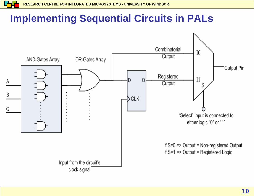
Implementing Sequential Circuits in PALs
10

RESEARCH CENTRE FOR INTEGRATED MICROSYSTEMS - UNIVERSITY OF WINDSOR
3- Generic Array Logic (GAL) GALs are very similar to PLAs and PALs except for the fact that
programmable connections are “MEMORY-controlled Switches”.
11

RESEARCH CENTRE FOR INTEGRATED MICROSYSTEMS - UNIVERSITY OF WINDSOR
Implementing Sequential Circuits in GALs Users can select the “Registered Output” by programming the
“Memory-controlled Programmable Multiplexer”.
12

RESEARCH CENTRE FOR INTEGRATED MICROSYSTEMS - UNIVERSITY OF WINDSOR
4- Complex PLD (CPLD) To provide large capacity devices, they integrated multiple Simple
PLDs (SPLDs) onto a single chip and provided PROGRAMMABLE interconnection to connect them together.
13

RESEARCH CENTRE FOR INTEGRATED MICROSYSTEMS - UNIVERSITY OF WINDSOR
Programmable Interconnection
14

RESEARCH CENTRE FOR INTEGRATED MICROSYSTEMS - UNIVERSITY OF WINDSOR
5- Look Up Table (LUT) based PLDs A B C D F 0 0 0 0 1 0 0 0 1 1 0 0 1 0 1 0 0 1 1 1 0 1 0 0 0 0 1 0 1 0 0 1 1 0 0 0 1 1 1 1 1 0 0 0 0 1 0 0 1 0 1 0 1 0 0 1 0 1 1 1 1 1 0 0 1 1 1 0 1 1 1 1 1 0 1 1 1 1 1 1
Design example:
15

RESEARCH CENTRE FOR INTEGRATED MICROSYSTEMS - UNIVERSITY OF WINDSOR
LUT-based PLDs (Cont’d)
12 ×N
12 ×N- For an N-input logic circuit, we need a LUT. - With a LUT we can implement different logic Functions!
N22
16

RESEARCH CENTRE FOR INTEGRATED MICROSYSTEMS - UNIVERSITY OF WINDSOR
An Example of Look-Up Table e.g. For an 2-input LUT (n=2) we can implement 16 different functions.
17

RESEARCH CENTRE FOR INTEGRATED MICROSYSTEMS - UNIVERSITY OF WINDSOR
LUT-Based Basic Logic Element (BLE) Instead of array of logic gates, there is a K-input LUT.
18

RESEARCH CENTRE FOR INTEGRATED MICROSYSTEMS - UNIVERSITY OF WINDSOR
6- Field Programmable Gate Arrays (FPGA) • FPGAs have got the highest logic capacities among PLDs • SRAM-based K-input LUTs (3≤K≤6) = A.K.A Logic Element (LE) • LEs are connected together using programmable interconnection.
19

RESEARCH CENTRE FOR INTEGRATED MICROSYSTEMS - UNIVERSITY OF WINDSOR
Interconnection (Routing) Architecture in FPGAs
20

RESEARCH CENTRE FOR INTEGRATED MICROSYSTEMS - UNIVERSITY OF WINDSOR
Real CPLD and FPGAs

RESEARCH CENTRE FOR INTEGRATED MICROSYSTEMS - UNIVERSITY OF WINDSOR
CPLD Applications
• Can construct reasonably complex designs
• Graphics controllers, LAN controllers, bus interface logic
• All CPLDs are re-programmable • Memory controlled switches, anti-fuses
• Some are re-programmable in circuit (ISP)
• e.g. modems allow new communication protocols to be downloaded

RESEARCH CENTRE FOR INTEGRATED MICROSYSTEMS - UNIVERSITY OF WINDSOR
FPGA Applications • Complex building blocks (ASIC replacement) in cellular base stations,
telecom switches, computer peripherals, high speed servers, instrumentation, etc.
• Any application in which cost, speed and power requirements are met!
RESEARCH CENTRE FOR INTEGRATED MICROSYSTEMS - UNIVERSITY OF WINDSOR
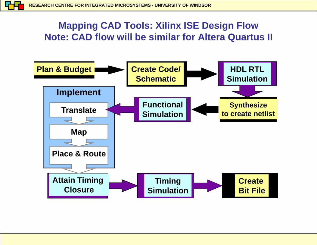
Mapping CAD Tools: Xilinx ISE Design Flow Note: CAD flow will be similar for Altera Quartus II
Translate
Map
Place & Route
Plan & Budget HDL RTL Simulation
Synthesize to create netlist
Functional Simulation
Create Bit File
Attain Timing Closure
Timing Simulation
Implement
Create Code/ Schematic

RESEARCH CENTRE FOR INTEGRATED MICROSYSTEMS - UNIVERSITY OF WINDSOR
What are we going to do in the Lab? 1- We will design (model and simulate) digital circuits using VHDL. 2- We will Compile & Synthesize the logic circuits using ALTERA®
QUARTUS II FPGA CAD tool. 3- We will be working with ALTERA® DE2 boards – see brochure
and user manual on course web site
21