
Research Article Low Actuating Voltage Spring-Free RF...
8
Research Article Low Actuating Voltage Spring-Free RF MEMS SPDT Switch Deepak Bansal, 1,2 Anuroop Bajpai, 1 Prem Kumar, 1 Maninder Kaur, 1 and Kamljit Rangra 1,2 1 Central Electronics Engineering Research Institute (CEERI), Council of Scientific and Industrial Research (CSIR), Pilani, Rajasthan 333031, India 2 Academy of Scientific and Innovative Research (AcSIR), New Delhi, India Correspondence should be addressed to Deepak Bansal; [email protected] Received 9 July 2016; Accepted 28 August 2016 Academic Editor: Jit S. Mandeep Copyright © 2016 Deepak Bansal et al. is is an open access article distributed under the Creative Commons Attribution License, which permits unrestricted use, distribution, and reproduction in any medium, provided the original work is properly cited. RF MEMS devices are known to be superior to their solid state counterparts in terms of power consumption and electromagnetic response. Major limitations of MEMS devices are their low switching speed, high actuation voltage, larger size, and reliability. In the present paper, a see-saw single pole double throw (SPDT) RF MEMS switch based on anchor-free mechanism is proposed which eliminates the above-mentioned disadvantages. e proposed switch has a switching time of 394 nsec with actuation voltage of 5 V. Size of the SPDT switch is reduced by utilizing a single series capacitive switch compared to conventional switches with capacitive and series combinations. Reliability of the switch is improved by adding floating metal and reducing stiction between the actuating bridge and transmission line. Insertion loss and isolation are better than −0.6 dB and −20 dB, respectively, for 1 GHz to 20 GHz applications. 1. Introduction Development of miniature wireless communications devices like mobile and satellite requires components with minimum power consumption with better performance. e RF MEMS devices are known to be better compared to solid state devices due to their low power consumption, high isolation, and low insertion loss. RF MEMS SPDT switches constitute the basic building block of the RF MEMS systems like SP4T [1], phase shiſter [2], switch matrix [3], other communication systems [4], and so forth. e RF MEMS devices are also known to have few drawbacks too, for example, low switching speed (20–200 sec), high pull-in voltage (15–80 V), larger size, and reliability [5, 6]. ese issues at present limit the utilization of the MEMS devices on a larger scale. ese mechanical parameters are function of spring constant and pull-in voltage. e conventional anchoring of a rectangular membrane is through two Euler beams where one end along the length is fixed to the membrane and the other to anchor post on either side of the membrane. When a voltage is applied between the movable and the fixed membrane of the switch as shown in Figure 1, the bridge moves down onto the fixed ground under the electrostatic force. At the pull-in voltage, the switch is in the down state [7] which is calculated using 1D lumped model as shown in Figure 1. From lumped model neglecting higher order effects as mentioned in [7], actuation voltage of the switch is given by = √ 8 3 27 , (1) where is spring constant and and are gap and area of overlap between the actuation electrode and the bridge. From (1), actuation voltage can be lowered by (i) increas- ing the overlap area (), (ii) decreasing the gap (), or (iii) decreasing spring constant (). Each method has its own demerits; for example, (i) large overlap area () enhances stiction forces as stiction is directly proportional to contact area [6, 8]. erefore, actuating electrode area is optimized based on stiction and restoring force [6]. Smaller gap () promotes stiction by reducing beam restoring force, which is proportional to the beam displace- ment. Smaller gap also adversely affects switch isolation through enhanced capacitive leakage. e bridge gap is also limited by the available fabrication technology and has been set in the range of 1–4 m. Hindawi Publishing Corporation Journal of Electrical and Computer Engineering Volume 2016, Article ID 7984548, 7 pages http://dx.doi.org/10.1155/2016/7984548
Transcript of Research Article Low Actuating Voltage Spring-Free RF...
Research ArticleLow Actuating Voltage Spring-Free RF MEMS SPDT Switch
Deepak Bansal12 Anuroop Bajpai1 Prem Kumar1 Maninder Kaur1 and Kamljit Rangra12
1Central Electronics Engineering Research Institute (CEERI) Council of Scientific and Industrial Research (CSIR) PilaniRajasthan 333031 India2Academy of Scientific and Innovative Research (AcSIR) New Delhi India
Correspondence should be addressed to Deepak Bansal dbansalpugmailcom
Received 9 July 2016 Accepted 28 August 2016
Academic Editor Jit S Mandeep
Copyright copy 2016 Deepak Bansal et alThis is an open access article distributed under the Creative Commons Attribution Licensewhich permits unrestricted use distribution and reproduction in any medium provided the original work is properly cited
RF MEMS devices are known to be superior to their solid state counterparts in terms of power consumption and electromagneticresponse Major limitations ofMEMS devices are their low switching speed high actuation voltage larger size and reliability In thepresent paper a see-saw single pole double throw (SPDT) RF MEMS switch based on anchor-free mechanism is proposed whicheliminates the above-mentioned disadvantagesThe proposed switch has a switching time of 394 nsec with actuation voltage of 5VSize of the SPDT switch is reduced by utilizing a single series capacitive switch compared to conventional switches with capacitiveand series combinations Reliability of the switch is improved by adding floating metal and reducing stiction between the actuatingbridge and transmission line Insertion loss and isolation are better than minus06 dB and minus20 dB respectively for 1 GHz to 20GHzapplications
1 Introduction
Development of miniature wireless communications deviceslike mobile and satellite requires components with minimumpower consumption with better performanceThe RFMEMSdevices are known to be better compared to solid state devicesdue to their low power consumption high isolation andlow insertion loss RF MEMS SPDT switches constitute thebasic building block of the RF MEMS systems like SP4T [1]phase shifter [2] switch matrix [3] other communicationsystems [4] and so forth The RF MEMS devices are alsoknown to have few drawbacks too for example low switchingspeed (20ndash200120583sec) high pull-in voltage (15ndash80V) largersize and reliability [5 6] These issues at present limit theutilization of the MEMS devices on a larger scale Thesemechanical parameters are function of spring constant andpull-in voltage The conventional anchoring of a rectangularmembrane is through two Euler beams where one endalong the length is fixed to the membrane and the otherto anchor post on either side of the membrane Whena voltage is applied between the movable and the fixedmembrane of the switch as shown in Figure 1 the bridgemoves down onto the fixed ground under the electrostaticforce At the pull-in voltage the switch is in the down state
[7] which is calculated using 1D lumped model as shown inFigure 1
From lumped model neglecting higher order effects asmentioned in [7] actuation voltage of the switch is given by
119881119901 =radic
8119896119892
3
27119860120576119900
(1)
where 119896 is spring constant and 119892 and 119860 are gap and area ofoverlap between the actuation electrode and the bridge
From (1) actuation voltage can be lowered by (i) increas-ing the overlap area (119860) (ii) decreasing the gap (119892) or (iii)decreasing spring constant (119896)
Each method has its own demerits for example (i) largeoverlap area (119860) enhances stiction forces as stiction is directlyproportional to contact area [6 8] Therefore actuatingelectrode area is optimized based on stiction and restoringforce [6]
Smaller gap (119892) promotes stiction by reducing beamrestoring force which is proportional to the beam displace-ment Smaller gap also adversely affects switch isolationthrough enhanced capacitive leakage The bridge gap is alsolimited by the available fabrication technology and has beenset in the range of 1ndash4 120583m
Hindawi Publishing CorporationJournal of Electrical and Computer EngineeringVolume 2016 Article ID 7984548 7 pageshttpdxdoiorg10115520167984548
2 Journal of Electrical and Computer Engineering
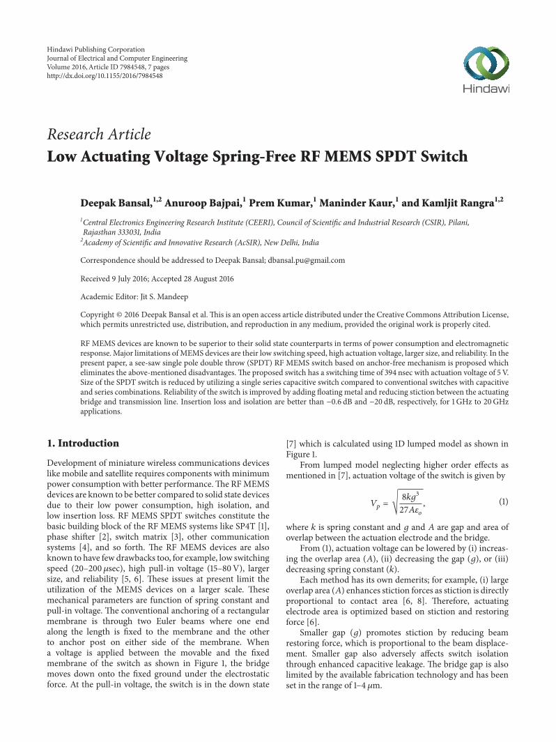
Bridge
k
g
+
minus
go
Figure 1 1D lumped model for actuation voltage calculation
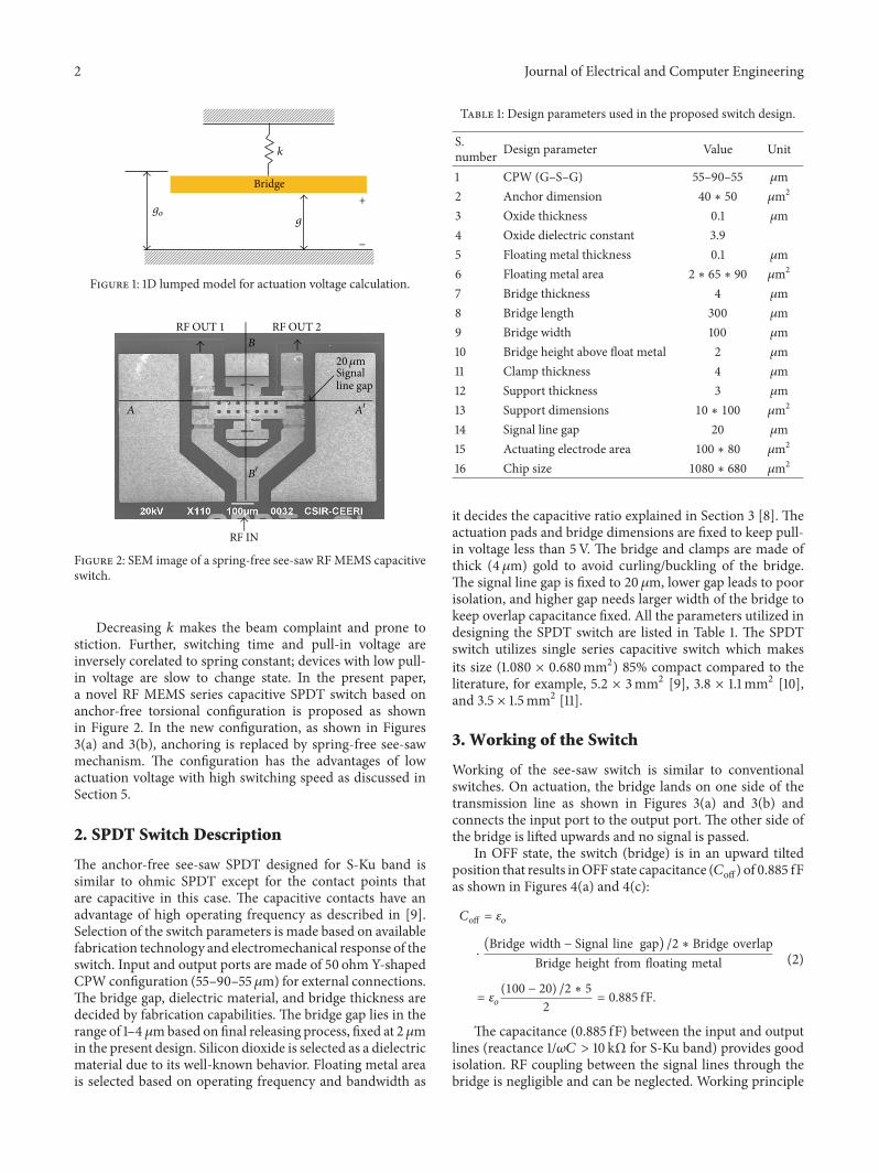
A
B
RF IN
RF OUT 2RF OUT 1
Signal line gap
A998400
B998400
20120583m
Figure 2 SEM image of a spring-free see-saw RFMEMS capacitiveswitch
Decreasing 119896 makes the beam complaint and prone tostiction Further switching time and pull-in voltage areinversely corelated to spring constant devices with low pull-in voltage are slow to change state In the present papera novel RF MEMS series capacitive SPDT switch based onanchor-free torsional configuration is proposed as shownin Figure 2 In the new configuration as shown in Figures3(a) and 3(b) anchoring is replaced by spring-free see-sawmechanism The configuration has the advantages of lowactuation voltage with high switching speed as discussed inSection 5
2 SPDT Switch Description
The anchor-free see-saw SPDT designed for S-Ku band issimilar to ohmic SPDT except for the contact points thatare capacitive in this case The capacitive contacts have anadvantage of high operating frequency as described in [9]Selection of the switch parameters is made based on availablefabrication technology and electromechanical response of theswitch Input and output ports are made of 50 ohm Y-shapedCPW configuration (55ndash90ndash55120583m) for external connectionsThe bridge gap dielectric material and bridge thickness aredecided by fabrication capabilities The bridge gap lies in therange of 1ndash4 120583mbased on final releasing process fixed at 2 120583min the present design Silicon dioxide is selected as a dielectricmaterial due to its well-known behavior Floating metal areais selected based on operating frequency and bandwidth as
Table 1 Design parameters used in the proposed switch design
Snumber Design parameter Value Unit
1 CPW (GndashSndashG) 55ndash90ndash55 120583m2 Anchor dimension 40 lowast 50 120583m2
3 Oxide thickness 01 120583m4 Oxide dielectric constant 395 Floating metal thickness 01 120583m6 Floating metal area 2 lowast 65 lowast 90 120583m2
7 Bridge thickness 4 120583m8 Bridge length 300 120583m9 Bridge width 100 120583m10 Bridge height above float metal 2 120583m11 Clamp thickness 4 120583m12 Support thickness 3 120583m13 Support dimensions 10 lowast 100 120583m2
14 Signal line gap 20 120583m15 Actuating electrode area 100 lowast 80 120583m2
16 Chip size 1080 lowast 680 120583m2
it decides the capacitive ratio explained in Section 3 [8] Theactuation pads and bridge dimensions are fixed to keep pull-in voltage less than 5V The bridge and clamps are made ofthick (4 120583m) gold to avoid curlingbuckling of the bridgeThe signal line gap is fixed to 20 120583m lower gap leads to poorisolation and higher gap needs larger width of the bridge tokeep overlap capacitance fixed All the parameters utilized indesigning the SPDT switch are listed in Table 1 The SPDTswitch utilizes single series capacitive switch which makesits size (1080 times 0680mm2) 85 compact compared to theliterature for example 52 times 3mm2 [9] 38 times 11mm2 [10]and 35 times 15mm2 [11]
3 Working of the Switch
Working of the see-saw switch is similar to conventionalswitches On actuation the bridge lands on one side of thetransmission line as shown in Figures 3(a) and 3(b) andconnects the input port to the output port The other side ofthe bridge is lifted upwards and no signal is passed
In OFF state the switch (bridge) is in an upward tiltedposition that results inOFF state capacitance (119862off ) of 0885 fFas shown in Figures 4(a) and 4(c)
119862off = 120576119900
sdot
(Bridge width minus Signal line gap) 2 lowast Bridge overlapBridge height from floating metal
= 120576119900
(100 minus 20) 2 lowast 5
2
= 0885 fF
(2)
The capacitance (0885 fF) between the input and outputlines (reactance 1120596119862 gt 10 kΩ for S-Ku band) provides goodisolation RF coupling between the signal lines through thebridge is negligible and can be neglected Working principle
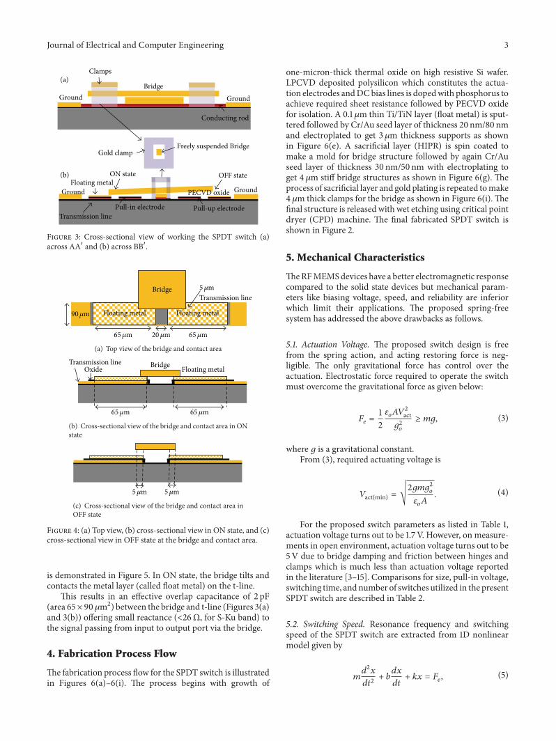
Journal of Electrical and Computer Engineering 3
PECVD oxideGround Ground
Pull-in electrode
Floating metal
Pull-up electrodeTransmission line
Freely suspended Bridge Gold clamp
BridgeGround Ground
Clamps(a)
(b)
Conducting rod
OFF state ON state
Figure 3 Cross-sectional view of working the SPDT switch (a)across AA1015840 and (b) across BB1015840
Floating metal Floating metal
Transmission lineBridge 5120583m
65120583m65120583m 20120583m
90120583m
(a) Top view of the bridge and contact area
BridgeOxide Floating metalTransmission line
65120583m65120583m
(b) Cross-sectional view of the bridge and contact area in ONstate
5120583m5120583m
(c) Cross-sectional view of the bridge and contact area inOFF state
Figure 4 (a) Top view (b) cross-sectional view in ON state and (c)cross-sectional view in OFF state at the bridge and contact area
is demonstrated in Figure 5 In ON state the bridge tilts andcontacts the metal layer (called float metal) on the t-line
This results in an effective overlap capacitance of 2 pF(area 65times 90120583m2) between the bridge and t-line (Figures 3(a)and 3(b)) offering small reactance (lt26Ω for S-Ku band) tothe signal passing from input to output port via the bridge
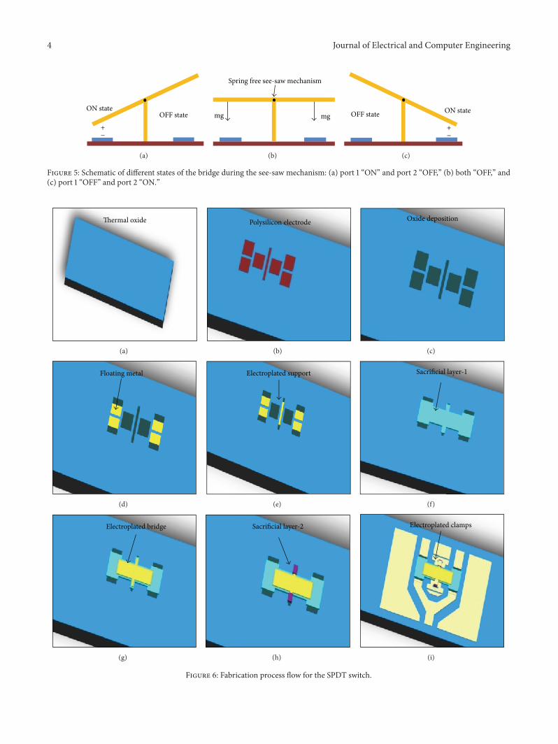
4 Fabrication Process Flow
The fabrication process flow for the SPDT switch is illustratedin Figures 6(a)ndash6(i) The process begins with growth of
one-micron-thick thermal oxide on high resistive Si waferLPCVD deposited polysilicon which constitutes the actua-tion electrodes andDCbias lines is dopedwith phosphorus toachieve required sheet resistance followed by PECVD oxidefor isolation A 01 120583m thin TiTiN layer (float metal) is sput-tered followed by CrAu seed layer of thickness 20 nm80 nmand electroplated to get 3120583m thickness supports as shownin Figure 6(e) A sacrificial layer (HIPR) is spin coated tomake a mold for bridge structure followed by again CrAuseed layer of thickness 30 nm50 nm with electroplating toget 4 120583m stiff bridge structures as shown in Figure 6(g) Theprocess of sacrificial layer and gold plating is repeated tomake4 120583m thick clamps for the bridge as shown in Figure 6(i) Thefinal structure is released with wet etching using critical pointdryer (CPD) machine The final fabricated SPDT switch isshown in Figure 2
5 Mechanical Characteristics
TheRFMEMSdevices have a better electromagnetic responsecompared to the solid state devices but mechanical param-eters like biasing voltage speed and reliability are inferiorwhich limit their applications The proposed spring-freesystem has addressed the above drawbacks as follows
51 Actuation Voltage The proposed switch design is freefrom the spring action and acting restoring force is neg-ligible The only gravitational force has control over theactuation Electrostatic force required to operate the switchmust overcome the gravitational force as given below
119865119890 =1
2
1205761199001198601198812
act119892
2119900
ge 119898119892(3)
where 119892 is a gravitational constantFrom (3) required actuating voltage is
119881act(min) = radic2119892119898119892
2
119900
120576119900119860
(4)
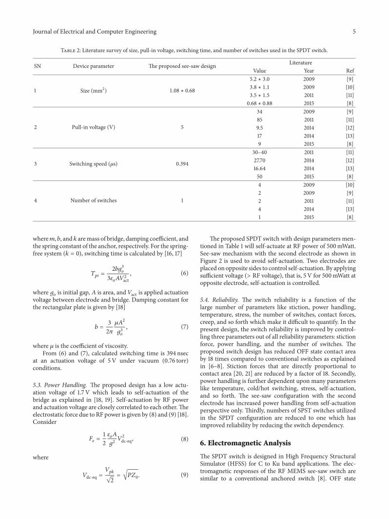
For the proposed switch parameters as listed in Table 1actuation voltage turns out to be 17 V However on measure-ments in open environment actuation voltage turns out to be5V due to bridge damping and friction between hinges andclamps which is much less than actuation voltage reportedin the literature [3ndash15] Comparisons for size pull-in voltageswitching time andnumber of switches utilized in the presentSPDT switch are described in Table 2
52 Switching Speed Resonance frequency and switchingspeed of the SPDT switch are extracted from 1D nonlinearmodel given by
119898
119889
2119909
119889119905
2+ 119887
119889119909
119889119905
+ 119896119909 = 119865119890(5)
4 Journal of Electrical and Computer Engineering
ON stateOFF state
+minus
(a)
Spring free see-saw mechanism
mgmg
(b)
OFF state ON state
+minus
(c)
Figure 5 Schematic of different states of the bridge during the see-saw mechanism (a) port 1 ldquoONrdquo and port 2 ldquoOFFrdquo (b) both ldquoOFFrdquo and(c) port 1 ldquoOFFrdquo and port 2 ldquoONrdquo
Thermal oxide
(a)
Polysilicon electrode
(b)
Oxide deposition
(c)
Floating metal
(d)
Electroplated support
(e)
Sacrificial layer-1
(f)
Electroplated bridge
(g)
Sacrificial layer-2
(h)
Electroplated clamps
(i)
Figure 6 Fabrication process flow for the SPDT switch
Journal of Electrical and Computer Engineering 5
Table 2 Literature survey of size pull-in voltage switching time and number of switches used in the SPDT switch
SN Device parameter The proposed see-saw design LiteratureValue Year Ref
1 Size (mm2) 108 lowast 068
52 lowast 30 2009 [9]38 lowast 11 2009 [10]35 lowast 15 2011 [11]068 lowast 088 2015 [8]
2 Pull-in voltage (V) 5
34 2009 [9]85 2011 [11]95 2014 [12]17 2014 [13]9 2015 [8]
3 Switching speed (120583s) 0394
30ndash40 2011 [11]2770 2014 [12]1664 2014 [13]50 2015 [8]
4 Number of switches 1
4 2009 [10]2 2009 [9]2 2011 [11]4 2014 [13]1 2015 [8]
where119898 119887 and 119896 aremass of bridge damping coefficient andthe spring constant of the anchor respectively For the spring-free system (119896 = 0) switching time is calculated by [16 17]
119879119901119894 =
2119887119892
3
119900
31205761199001198601198812act
(6)
where 119892119900 is initial gap 119860 is area and 119881act is applied actuationvoltage between electrode and bridge Damping constant forthe rectangular plate is given by [18]
119887 =
3
2120587
120583119860
2
119892
3119900
(7)
where 120583 is the coefficient of viscosityFrom (6) and (7) calculated switching time is 394 nsec
at an actuation voltage of 5V under vacuum (076 torr)conditions
53 Power Handling The proposed design has a low actu-ation voltage of 17 V which leads to self-actuation of thebridge as explained in [18 19] Self-actuation by RF powerand actuation voltage are closely correlated to each otherTheelectrostatic force due to RF power is given by (8) and (9) [18]Consider
119865119890 =1
2
120576119900119860
119892
2119881
2
dc-eq (8)
where
119881dc-eq =119881119901119896
radic
2
=
radic
1198751198850(9)
The proposed SPDT switch with design parameters men-tioned in Table 1 will self-actuate at RF power of 500mWattSee-saw mechanism with the second electrode as shown inFigure 2 is used to avoid self-actuation Two electrodes areplaced on opposite sides to control self-actuation By applyingsufficient voltage (gt RF voltage) that is 5 V for 500mWatt atopposite electrode self-actuation is controlled
54 Reliability The switch reliability is a function of thelarge number of parameters like stiction power handlingtemperature stress the number of switches contact forcescreep and so forth which make it difficult to quantify In thepresent design the switch reliability is improved by control-ling three parameters out of all reliability parameters stictionforce power handling and the number of switches Theproposed switch design has reduced OFF state contact areaby 18 times compared to conventional switches as explainedin [6ndash8] Stiction forces that are directly proportional tocontact area [20 21] are reduced by a factor of 18 Secondlypower handling is further dependent upon many parameterslike temperature coldhot switching stress self-actuationand so forth The see-saw configuration with the secondelectrode has increased power handling from self-actuationperspective only Thirdly numbers of SPST switches utilizedin the SPDT configuration are reduced to one which hasimproved reliability by reducing the switch dependency
6 Electromagnetic Analysis
The SPDT switch is designed in High Frequency StructuralSimulator (HFSS) for C to Ku band applications The elec-tromagnetic responses of the RF MEMS see-saw switch aresimilar to a conventional anchored switch [8] OFF state
6 Journal of Electrical and Computer Engineering
IsolationInsertion loss
ON state
OFF state
10 200Frequency (GHz)
S 21
(dB)
minus40
minus30
minus20
minus10
0
Figure 7 Measured 119878-parameter response of the SPDT switch
overlap capacitance is reduced to 0885 fF with floating metalthat improves the insertion loss [8] and parasitic capacitancewhich also lies in the range of femto-Farad increases its valueto 19 fF In the ON state overlap capacitance is 201 pF andparasitics have a negligible effect on it Insertion loss lies inthe range of minus03 dB to minus06 dB for a wide bandwidth of 19 (1ndash20)GHz Isolation varies from minus281 dB (1GHz) to minus20 dB(20GHz) as shown in Figure 7
7 Conclusions
The anchor-free see-saw RF MEMS SPDT switch is fabri-cated using a single series capacitive switch with compactdimensions of 0734mm2 The proposed switch has a lowactuation voltage of 5Vwith high switching speed (394 nsec)Insertion loss and isolation are better than minus06 dB andminus20 dB respectively in the frequency range of 1 GHz to20GHz
Competing Interests
The authors declare that they have no conflict of interests orfinancial conflicts to disclose
Acknowledgments
The authors would like to thank CSIR India for providingfinancial support under Budget Head PSC-0201
References
[1] G Hu Z Liu Y Qiao et al ldquoBonding packaging of a SP4TRF MEMS switchrdquo in Proceedings of the 7th InternationalConference on Electronics Packaging Technology (ICEPT rsquo06) pp1ndash4 IEEE Shanghai China August 2006
[2] G L Tan R E Mihailovich J B Hacker J F DeNataleand G M Rebeiz ldquoA very-low-loss 2-bit X-band RF MEMSphase shiftersrdquo in Proceedings of the IEEE MTT-S InternationalMicrowave Symposium Digest vol 1 pp 333ndash335 Seattle WashUSA 2002
[3] M Daneshmand and R R Mansour ldquoC-type and R-type RFMEMS switches for redundancy switch matrix applicationrdquo inProceedings of the IEEE International Microwave SymposiumDigest (MTT-S rsquo06) pp 144ndash147 2006
[4] M H Misran N A Shairi G H The and M A Meor SaidldquoDesign and performance analysis of single biasing based SPDTswitch for wireless data communicationsrdquo in Proceedings of the5th IEEE Asia-Pacific Conference on Applied Electromagnetics(APACE rsquo12) pp 363ndash366 Melaka Malaysia December 2012
[5] G M Rebeiz and J B Muldavin ldquoRF MEMS switches andswitch circuitsrdquo IEEEMicrowaveMagazine vol 2 no 4 pp 59ndash71 2001
[6] D Bansal A Bajpai P Kumar A Kumar M Kaur and KRangra ldquoDesign and fabrication of a reduced stiction radiofrequency MEMS switchrdquo Journal of MicroNanolithographyMEMS and MOEMS vol 14 no 3 Article ID 035002 2015
[7] L X Zhang and Y-P Zhao ldquoElectromechanical model of RFMEMS switchesrdquo Microsystem Technologies vol 9 no 6-7 pp420ndash426 2003
[8] D Bansal A Kumar A Sharma and K J Rangra ldquoDesign ofcompact and wide bandwidth SPDTwith anti-stiction torsionalRF MEMS series capacitive switchrdquo Microsystem TechnologiesJournal vol 21 no 5 pp 1047ndash1052 2015
[9] Y Uno K Narise T Masuda et al ldquoDevelopment of SPDT-structured RF MEMS switchrdquo in Proceedings of the 15thInternational Conference on Solid-State Sensors Actuators andMicrosystems (TRANSDUCERS rsquo09) pp 541ndash544 June 2009
[10] S Cheng P Rantakari R Malmqvist et al ldquoSwitched beamantenna based on RFMEMS SPDT switch on quartz substraterdquoIEEE Antennas andWireless Propagation Letters vol 8 pp 383ndash386 2009
[11] D Yamane W Sun H Fujita H Toshiyoshi and S KawasakildquoDevelopment of a Dual-SPDTRF-MEMS switch for Ku-bandrdquoinProceedings of the IEEERadio andWireless Symposium (RWWrsquo10) pp 432ndash435 New Orleans La USA January 2010
[12] U K Kommuri ldquoDesign of low voltage RF MEMS switch at 35GHzrdquoMicrowave and Optical Technology Letters vol 56 no 6pp 1483ndash1486 2014
[13] U Sharma M Kumar K K Jain and R K Bhan ldquoBroadbanddesign of RF MEMS SPDT switchrdquo International Journal ofEngineering Sciences amp Emerging Technologies vol 6 no 4 pp405ndash409 2014
[14] R Marcelli G Bartolucci G Minucci B Margesin F Giaco-mozzi and F Vitulli ldquoLumped element modeling of coplanarseries RF MEMS switchesrdquo Electronics Letters vol 40 no 20pp 1272ndash1274 2004
[15] D Bansal A Kumar A Sharma P Kumar and K J RangraldquoDesign of novel compact anti-stiction and low insertion lossRF MEMS switchrdquoMicrosystem Technologies vol 20 no 2 pp337ndash340 2014
[16] R K Gupta and S D Senturia ldquoPull-in time dynamics as ameasure of absolute pressurerdquo in Proceedings of the 10th AnnualInternational Workshop on Micro Electro Mechanical Systems(MEMS rsquo97) pp 290ndash294 Nagoya Japan January 1997
[17] S Dushman and J Lagerty Scientific Foundations of VacuumTechnique John Wiley amp Sons New York NY USA 1962
Journal of Electrical and Computer Engineering 7
[18] G M Rebeiz RF MEMS Theory Design and Technology JohnWiley amp Sons Hoboken NJ USA 2003
[19] R Malmqvist R Jonsson C Samuelsson et al ldquoSelf-actuationtests of ohmic contact and capacitive RFMEMS switches forwideband RF power limiter circuitsrdquo in Proceedings of the 35thInternational Semiconductor Conference (CAS rsquo12) pp 217ndash220IEEE Sinaia Romania October 2012
[20] N Tas T Sonnenberg H Jansen R Legtenberg and MElwenspoek ldquoStiction in surface micromachiningrdquo Journal ofMicromechanics andMicroengineering vol 6 no 4 pp 385ndash3971996
[21] Y-P Zhao L S Wang and T X Yu ldquoMechanics of adhesion inMEMSmdasha reviewrdquo Journal of Adhesion Science and Technologyvol 17 no 4 pp 519ndash546 2003
International Journal of
AerospaceEngineeringHindawi Publishing Corporationhttpwwwhindawicom Volume 2014
RoboticsJournal of
Hindawi Publishing Corporationhttpwwwhindawicom Volume 2014
Hindawi Publishing Corporationhttpwwwhindawicom Volume 2014
Active and Passive Electronic Components
Control Scienceand Engineering
Journal of
Hindawi Publishing Corporationhttpwwwhindawicom Volume 2014
International Journal of
RotatingMachinery
Hindawi Publishing Corporationhttpwwwhindawicom Volume 2014
Hindawi Publishing Corporation httpwwwhindawicom
Journal ofEngineeringVolume 2014
Submit your manuscripts athttpwwwhindawicom
VLSI Design
Hindawi Publishing Corporationhttpwwwhindawicom Volume 2014
Hindawi Publishing Corporationhttpwwwhindawicom Volume 2014
Shock and Vibration
Hindawi Publishing Corporationhttpwwwhindawicom Volume 2014
Civil EngineeringAdvances in
Acoustics and VibrationAdvances in
Hindawi Publishing Corporationhttpwwwhindawicom Volume 2014
Hindawi Publishing Corporationhttpwwwhindawicom Volume 2014
Electrical and Computer Engineering
Journal of
Advances inOptoElectronics
Hindawi Publishing Corporation httpwwwhindawicom
Volume 2014
The Scientific World JournalHindawi Publishing Corporation httpwwwhindawicom Volume 2014
SensorsJournal of
Hindawi Publishing Corporationhttpwwwhindawicom Volume 2014
Modelling amp Simulation in EngineeringHindawi Publishing Corporation httpwwwhindawicom Volume 2014
Hindawi Publishing Corporationhttpwwwhindawicom Volume 2014
Chemical EngineeringInternational Journal of Antennas and
Propagation
International Journal of
Hindawi Publishing Corporationhttpwwwhindawicom Volume 2014
Hindawi Publishing Corporationhttpwwwhindawicom Volume 2014
Navigation and Observation
International Journal of
Hindawi Publishing Corporationhttpwwwhindawicom Volume 2014
DistributedSensor Networks
International Journal of
2 Journal of Electrical and Computer Engineering
Bridge
k
g
+
minus
go
Figure 1 1D lumped model for actuation voltage calculation
A
B
RF IN
RF OUT 2RF OUT 1
Signal line gap
A998400
B998400
20120583m
Figure 2 SEM image of a spring-free see-saw RFMEMS capacitiveswitch
Decreasing 119896 makes the beam complaint and prone tostiction Further switching time and pull-in voltage areinversely corelated to spring constant devices with low pull-in voltage are slow to change state In the present papera novel RF MEMS series capacitive SPDT switch based onanchor-free torsional configuration is proposed as shownin Figure 2 In the new configuration as shown in Figures3(a) and 3(b) anchoring is replaced by spring-free see-sawmechanism The configuration has the advantages of lowactuation voltage with high switching speed as discussed inSection 5
2 SPDT Switch Description
The anchor-free see-saw SPDT designed for S-Ku band issimilar to ohmic SPDT except for the contact points thatare capacitive in this case The capacitive contacts have anadvantage of high operating frequency as described in [9]Selection of the switch parameters is made based on availablefabrication technology and electromechanical response of theswitch Input and output ports are made of 50 ohm Y-shapedCPW configuration (55ndash90ndash55120583m) for external connectionsThe bridge gap dielectric material and bridge thickness aredecided by fabrication capabilities The bridge gap lies in therange of 1ndash4 120583mbased on final releasing process fixed at 2 120583min the present design Silicon dioxide is selected as a dielectricmaterial due to its well-known behavior Floating metal areais selected based on operating frequency and bandwidth as
Table 1 Design parameters used in the proposed switch design
Snumber Design parameter Value Unit
1 CPW (GndashSndashG) 55ndash90ndash55 120583m2 Anchor dimension 40 lowast 50 120583m2
3 Oxide thickness 01 120583m4 Oxide dielectric constant 395 Floating metal thickness 01 120583m6 Floating metal area 2 lowast 65 lowast 90 120583m2
7 Bridge thickness 4 120583m8 Bridge length 300 120583m9 Bridge width 100 120583m10 Bridge height above float metal 2 120583m11 Clamp thickness 4 120583m12 Support thickness 3 120583m13 Support dimensions 10 lowast 100 120583m2
14 Signal line gap 20 120583m15 Actuating electrode area 100 lowast 80 120583m2
16 Chip size 1080 lowast 680 120583m2
it decides the capacitive ratio explained in Section 3 [8] Theactuation pads and bridge dimensions are fixed to keep pull-in voltage less than 5V The bridge and clamps are made ofthick (4 120583m) gold to avoid curlingbuckling of the bridgeThe signal line gap is fixed to 20 120583m lower gap leads to poorisolation and higher gap needs larger width of the bridge tokeep overlap capacitance fixed All the parameters utilized indesigning the SPDT switch are listed in Table 1 The SPDTswitch utilizes single series capacitive switch which makesits size (1080 times 0680mm2) 85 compact compared to theliterature for example 52 times 3mm2 [9] 38 times 11mm2 [10]and 35 times 15mm2 [11]
3 Working of the Switch
Working of the see-saw switch is similar to conventionalswitches On actuation the bridge lands on one side of thetransmission line as shown in Figures 3(a) and 3(b) andconnects the input port to the output port The other side ofthe bridge is lifted upwards and no signal is passed
In OFF state the switch (bridge) is in an upward tiltedposition that results inOFF state capacitance (119862off ) of 0885 fFas shown in Figures 4(a) and 4(c)
119862off = 120576119900
sdot
(Bridge width minus Signal line gap) 2 lowast Bridge overlapBridge height from floating metal
= 120576119900
(100 minus 20) 2 lowast 5
2
= 0885 fF
(2)
The capacitance (0885 fF) between the input and outputlines (reactance 1120596119862 gt 10 kΩ for S-Ku band) provides goodisolation RF coupling between the signal lines through thebridge is negligible and can be neglected Working principle
Journal of Electrical and Computer Engineering 3
PECVD oxideGround Ground
Pull-in electrode
Floating metal
Pull-up electrodeTransmission line
Freely suspended Bridge Gold clamp
BridgeGround Ground
Clamps(a)
(b)
Conducting rod
OFF state ON state
Figure 3 Cross-sectional view of working the SPDT switch (a)across AA1015840 and (b) across BB1015840
Floating metal Floating metal
Transmission lineBridge 5120583m
65120583m65120583m 20120583m
90120583m
(a) Top view of the bridge and contact area
BridgeOxide Floating metalTransmission line
65120583m65120583m
(b) Cross-sectional view of the bridge and contact area in ONstate
5120583m5120583m
(c) Cross-sectional view of the bridge and contact area inOFF state
Figure 4 (a) Top view (b) cross-sectional view in ON state and (c)cross-sectional view in OFF state at the bridge and contact area
is demonstrated in Figure 5 In ON state the bridge tilts andcontacts the metal layer (called float metal) on the t-line
This results in an effective overlap capacitance of 2 pF(area 65times 90120583m2) between the bridge and t-line (Figures 3(a)and 3(b)) offering small reactance (lt26Ω for S-Ku band) tothe signal passing from input to output port via the bridge
4 Fabrication Process Flow
The fabrication process flow for the SPDT switch is illustratedin Figures 6(a)ndash6(i) The process begins with growth of
one-micron-thick thermal oxide on high resistive Si waferLPCVD deposited polysilicon which constitutes the actua-tion electrodes andDCbias lines is dopedwith phosphorus toachieve required sheet resistance followed by PECVD oxidefor isolation A 01 120583m thin TiTiN layer (float metal) is sput-tered followed by CrAu seed layer of thickness 20 nm80 nmand electroplated to get 3120583m thickness supports as shownin Figure 6(e) A sacrificial layer (HIPR) is spin coated tomake a mold for bridge structure followed by again CrAuseed layer of thickness 30 nm50 nm with electroplating toget 4 120583m stiff bridge structures as shown in Figure 6(g) Theprocess of sacrificial layer and gold plating is repeated tomake4 120583m thick clamps for the bridge as shown in Figure 6(i) Thefinal structure is released with wet etching using critical pointdryer (CPD) machine The final fabricated SPDT switch isshown in Figure 2
5 Mechanical Characteristics
TheRFMEMSdevices have a better electromagnetic responsecompared to the solid state devices but mechanical param-eters like biasing voltage speed and reliability are inferiorwhich limit their applications The proposed spring-freesystem has addressed the above drawbacks as follows
51 Actuation Voltage The proposed switch design is freefrom the spring action and acting restoring force is neg-ligible The only gravitational force has control over theactuation Electrostatic force required to operate the switchmust overcome the gravitational force as given below
119865119890 =1
2
1205761199001198601198812
act119892
2119900
ge 119898119892(3)
where 119892 is a gravitational constantFrom (3) required actuating voltage is
119881act(min) = radic2119892119898119892
2
119900
120576119900119860
(4)
For the proposed switch parameters as listed in Table 1actuation voltage turns out to be 17 V However on measure-ments in open environment actuation voltage turns out to be5V due to bridge damping and friction between hinges andclamps which is much less than actuation voltage reportedin the literature [3ndash15] Comparisons for size pull-in voltageswitching time andnumber of switches utilized in the presentSPDT switch are described in Table 2
52 Switching Speed Resonance frequency and switchingspeed of the SPDT switch are extracted from 1D nonlinearmodel given by
119898
119889
2119909
119889119905
2+ 119887
119889119909
119889119905
+ 119896119909 = 119865119890(5)
4 Journal of Electrical and Computer Engineering
ON stateOFF state
+minus
(a)
Spring free see-saw mechanism
mgmg
(b)
OFF state ON state
+minus
(c)
Figure 5 Schematic of different states of the bridge during the see-saw mechanism (a) port 1 ldquoONrdquo and port 2 ldquoOFFrdquo (b) both ldquoOFFrdquo and(c) port 1 ldquoOFFrdquo and port 2 ldquoONrdquo
Thermal oxide
(a)
Polysilicon electrode
(b)
Oxide deposition
(c)
Floating metal
(d)
Electroplated support
(e)
Sacrificial layer-1
(f)
Electroplated bridge
(g)
Sacrificial layer-2
(h)
Electroplated clamps
(i)
Figure 6 Fabrication process flow for the SPDT switch
Journal of Electrical and Computer Engineering 5
Table 2 Literature survey of size pull-in voltage switching time and number of switches used in the SPDT switch
SN Device parameter The proposed see-saw design LiteratureValue Year Ref
1 Size (mm2) 108 lowast 068
52 lowast 30 2009 [9]38 lowast 11 2009 [10]35 lowast 15 2011 [11]068 lowast 088 2015 [8]
2 Pull-in voltage (V) 5
34 2009 [9]85 2011 [11]95 2014 [12]17 2014 [13]9 2015 [8]
3 Switching speed (120583s) 0394
30ndash40 2011 [11]2770 2014 [12]1664 2014 [13]50 2015 [8]
4 Number of switches 1
4 2009 [10]2 2009 [9]2 2011 [11]4 2014 [13]1 2015 [8]
where119898 119887 and 119896 aremass of bridge damping coefficient andthe spring constant of the anchor respectively For the spring-free system (119896 = 0) switching time is calculated by [16 17]
119879119901119894 =
2119887119892
3
119900
31205761199001198601198812act
(6)
where 119892119900 is initial gap 119860 is area and 119881act is applied actuationvoltage between electrode and bridge Damping constant forthe rectangular plate is given by [18]
119887 =
3
2120587
120583119860
2
119892
3119900
(7)
where 120583 is the coefficient of viscosityFrom (6) and (7) calculated switching time is 394 nsec
at an actuation voltage of 5V under vacuum (076 torr)conditions
53 Power Handling The proposed design has a low actu-ation voltage of 17 V which leads to self-actuation of thebridge as explained in [18 19] Self-actuation by RF powerand actuation voltage are closely correlated to each otherTheelectrostatic force due to RF power is given by (8) and (9) [18]Consider
119865119890 =1
2
120576119900119860
119892
2119881
2
dc-eq (8)
where
119881dc-eq =119881119901119896
radic
2
=
radic
1198751198850(9)
The proposed SPDT switch with design parameters men-tioned in Table 1 will self-actuate at RF power of 500mWattSee-saw mechanism with the second electrode as shown inFigure 2 is used to avoid self-actuation Two electrodes areplaced on opposite sides to control self-actuation By applyingsufficient voltage (gt RF voltage) that is 5 V for 500mWatt atopposite electrode self-actuation is controlled
54 Reliability The switch reliability is a function of thelarge number of parameters like stiction power handlingtemperature stress the number of switches contact forcescreep and so forth which make it difficult to quantify In thepresent design the switch reliability is improved by control-ling three parameters out of all reliability parameters stictionforce power handling and the number of switches Theproposed switch design has reduced OFF state contact areaby 18 times compared to conventional switches as explainedin [6ndash8] Stiction forces that are directly proportional tocontact area [20 21] are reduced by a factor of 18 Secondlypower handling is further dependent upon many parameterslike temperature coldhot switching stress self-actuationand so forth The see-saw configuration with the secondelectrode has increased power handling from self-actuationperspective only Thirdly numbers of SPST switches utilizedin the SPDT configuration are reduced to one which hasimproved reliability by reducing the switch dependency
6 Electromagnetic Analysis
The SPDT switch is designed in High Frequency StructuralSimulator (HFSS) for C to Ku band applications The elec-tromagnetic responses of the RF MEMS see-saw switch aresimilar to a conventional anchored switch [8] OFF state
6 Journal of Electrical and Computer Engineering
IsolationInsertion loss
ON state
OFF state
10 200Frequency (GHz)
S 21
(dB)
minus40
minus30
minus20
minus10
0
Figure 7 Measured 119878-parameter response of the SPDT switch
overlap capacitance is reduced to 0885 fF with floating metalthat improves the insertion loss [8] and parasitic capacitancewhich also lies in the range of femto-Farad increases its valueto 19 fF In the ON state overlap capacitance is 201 pF andparasitics have a negligible effect on it Insertion loss lies inthe range of minus03 dB to minus06 dB for a wide bandwidth of 19 (1ndash20)GHz Isolation varies from minus281 dB (1GHz) to minus20 dB(20GHz) as shown in Figure 7
7 Conclusions
The anchor-free see-saw RF MEMS SPDT switch is fabri-cated using a single series capacitive switch with compactdimensions of 0734mm2 The proposed switch has a lowactuation voltage of 5Vwith high switching speed (394 nsec)Insertion loss and isolation are better than minus06 dB andminus20 dB respectively in the frequency range of 1 GHz to20GHz
Competing Interests
The authors declare that they have no conflict of interests orfinancial conflicts to disclose
Acknowledgments
The authors would like to thank CSIR India for providingfinancial support under Budget Head PSC-0201
References
[1] G Hu Z Liu Y Qiao et al ldquoBonding packaging of a SP4TRF MEMS switchrdquo in Proceedings of the 7th InternationalConference on Electronics Packaging Technology (ICEPT rsquo06) pp1ndash4 IEEE Shanghai China August 2006
[2] G L Tan R E Mihailovich J B Hacker J F DeNataleand G M Rebeiz ldquoA very-low-loss 2-bit X-band RF MEMSphase shiftersrdquo in Proceedings of the IEEE MTT-S InternationalMicrowave Symposium Digest vol 1 pp 333ndash335 Seattle WashUSA 2002
[3] M Daneshmand and R R Mansour ldquoC-type and R-type RFMEMS switches for redundancy switch matrix applicationrdquo inProceedings of the IEEE International Microwave SymposiumDigest (MTT-S rsquo06) pp 144ndash147 2006
[4] M H Misran N A Shairi G H The and M A Meor SaidldquoDesign and performance analysis of single biasing based SPDTswitch for wireless data communicationsrdquo in Proceedings of the5th IEEE Asia-Pacific Conference on Applied Electromagnetics(APACE rsquo12) pp 363ndash366 Melaka Malaysia December 2012
[5] G M Rebeiz and J B Muldavin ldquoRF MEMS switches andswitch circuitsrdquo IEEEMicrowaveMagazine vol 2 no 4 pp 59ndash71 2001
[6] D Bansal A Bajpai P Kumar A Kumar M Kaur and KRangra ldquoDesign and fabrication of a reduced stiction radiofrequency MEMS switchrdquo Journal of MicroNanolithographyMEMS and MOEMS vol 14 no 3 Article ID 035002 2015
[7] L X Zhang and Y-P Zhao ldquoElectromechanical model of RFMEMS switchesrdquo Microsystem Technologies vol 9 no 6-7 pp420ndash426 2003
[8] D Bansal A Kumar A Sharma and K J Rangra ldquoDesign ofcompact and wide bandwidth SPDTwith anti-stiction torsionalRF MEMS series capacitive switchrdquo Microsystem TechnologiesJournal vol 21 no 5 pp 1047ndash1052 2015
[9] Y Uno K Narise T Masuda et al ldquoDevelopment of SPDT-structured RF MEMS switchrdquo in Proceedings of the 15thInternational Conference on Solid-State Sensors Actuators andMicrosystems (TRANSDUCERS rsquo09) pp 541ndash544 June 2009
[10] S Cheng P Rantakari R Malmqvist et al ldquoSwitched beamantenna based on RFMEMS SPDT switch on quartz substraterdquoIEEE Antennas andWireless Propagation Letters vol 8 pp 383ndash386 2009
[11] D Yamane W Sun H Fujita H Toshiyoshi and S KawasakildquoDevelopment of a Dual-SPDTRF-MEMS switch for Ku-bandrdquoinProceedings of the IEEERadio andWireless Symposium (RWWrsquo10) pp 432ndash435 New Orleans La USA January 2010
[12] U K Kommuri ldquoDesign of low voltage RF MEMS switch at 35GHzrdquoMicrowave and Optical Technology Letters vol 56 no 6pp 1483ndash1486 2014
[13] U Sharma M Kumar K K Jain and R K Bhan ldquoBroadbanddesign of RF MEMS SPDT switchrdquo International Journal ofEngineering Sciences amp Emerging Technologies vol 6 no 4 pp405ndash409 2014
[14] R Marcelli G Bartolucci G Minucci B Margesin F Giaco-mozzi and F Vitulli ldquoLumped element modeling of coplanarseries RF MEMS switchesrdquo Electronics Letters vol 40 no 20pp 1272ndash1274 2004
[15] D Bansal A Kumar A Sharma P Kumar and K J RangraldquoDesign of novel compact anti-stiction and low insertion lossRF MEMS switchrdquoMicrosystem Technologies vol 20 no 2 pp337ndash340 2014
[16] R K Gupta and S D Senturia ldquoPull-in time dynamics as ameasure of absolute pressurerdquo in Proceedings of the 10th AnnualInternational Workshop on Micro Electro Mechanical Systems(MEMS rsquo97) pp 290ndash294 Nagoya Japan January 1997
[17] S Dushman and J Lagerty Scientific Foundations of VacuumTechnique John Wiley amp Sons New York NY USA 1962
Journal of Electrical and Computer Engineering 7
[18] G M Rebeiz RF MEMS Theory Design and Technology JohnWiley amp Sons Hoboken NJ USA 2003
[19] R Malmqvist R Jonsson C Samuelsson et al ldquoSelf-actuationtests of ohmic contact and capacitive RFMEMS switches forwideband RF power limiter circuitsrdquo in Proceedings of the 35thInternational Semiconductor Conference (CAS rsquo12) pp 217ndash220IEEE Sinaia Romania October 2012
[20] N Tas T Sonnenberg H Jansen R Legtenberg and MElwenspoek ldquoStiction in surface micromachiningrdquo Journal ofMicromechanics andMicroengineering vol 6 no 4 pp 385ndash3971996
[21] Y-P Zhao L S Wang and T X Yu ldquoMechanics of adhesion inMEMSmdasha reviewrdquo Journal of Adhesion Science and Technologyvol 17 no 4 pp 519ndash546 2003
International Journal of
AerospaceEngineeringHindawi Publishing Corporationhttpwwwhindawicom Volume 2014
RoboticsJournal of
Hindawi Publishing Corporationhttpwwwhindawicom Volume 2014
Hindawi Publishing Corporationhttpwwwhindawicom Volume 2014
Active and Passive Electronic Components
Control Scienceand Engineering
Journal of
Hindawi Publishing Corporationhttpwwwhindawicom Volume 2014
International Journal of
RotatingMachinery
Hindawi Publishing Corporationhttpwwwhindawicom Volume 2014
Hindawi Publishing Corporation httpwwwhindawicom
Journal ofEngineeringVolume 2014
Submit your manuscripts athttpwwwhindawicom
VLSI Design
Hindawi Publishing Corporationhttpwwwhindawicom Volume 2014
Hindawi Publishing Corporationhttpwwwhindawicom Volume 2014
Shock and Vibration
Hindawi Publishing Corporationhttpwwwhindawicom Volume 2014
Civil EngineeringAdvances in
Acoustics and VibrationAdvances in
Hindawi Publishing Corporationhttpwwwhindawicom Volume 2014
Hindawi Publishing Corporationhttpwwwhindawicom Volume 2014
Electrical and Computer Engineering
Journal of
Advances inOptoElectronics
Hindawi Publishing Corporation httpwwwhindawicom
Volume 2014
The Scientific World JournalHindawi Publishing Corporation httpwwwhindawicom Volume 2014
SensorsJournal of
Hindawi Publishing Corporationhttpwwwhindawicom Volume 2014
Modelling amp Simulation in EngineeringHindawi Publishing Corporation httpwwwhindawicom Volume 2014
Hindawi Publishing Corporationhttpwwwhindawicom Volume 2014
Chemical EngineeringInternational Journal of Antennas and
Propagation
International Journal of
Hindawi Publishing Corporationhttpwwwhindawicom Volume 2014
Hindawi Publishing Corporationhttpwwwhindawicom Volume 2014
Navigation and Observation
International Journal of
Hindawi Publishing Corporationhttpwwwhindawicom Volume 2014
DistributedSensor Networks
International Journal of

International Journal of
AerospaceEngineeringHindawi Publishing Corporationhttpwwwhindawicom Volume 2014
RoboticsJournal of
Hindawi Publishing Corporationhttpwwwhindawicom Volume 2014
Hindawi Publishing Corporationhttpwwwhindawicom Volume 2014
Active and Passive Electronic Components
Control Scienceand Engineering
Journal of
Hindawi Publishing Corporationhttpwwwhindawicom Volume 2014
International Journal of
RotatingMachinery
Hindawi Publishing Corporationhttpwwwhindawicom Volume 2014
Hindawi Publishing Corporation httpwwwhindawicom
Journal ofEngineeringVolume 2014
Submit your manuscripts athttpwwwhindawicom
VLSI Design
Hindawi Publishing Corporationhttpwwwhindawicom Volume 2014
Hindawi Publishing Corporationhttpwwwhindawicom Volume 2014
Shock and Vibration
Hindawi Publishing Corporationhttpwwwhindawicom Volume 2014
Civil EngineeringAdvances in
Acoustics and VibrationAdvances in
Hindawi Publishing Corporationhttpwwwhindawicom Volume 2014
Hindawi Publishing Corporationhttpwwwhindawicom Volume 2014
Electrical and Computer Engineering
Journal of
Advances inOptoElectronics
Hindawi Publishing Corporation httpwwwhindawicom
Volume 2014
The Scientific World JournalHindawi Publishing Corporation httpwwwhindawicom Volume 2014
SensorsJournal of
Hindawi Publishing Corporationhttpwwwhindawicom Volume 2014
Modelling amp Simulation in EngineeringHindawi Publishing Corporation httpwwwhindawicom Volume 2014
Hindawi Publishing Corporationhttpwwwhindawicom Volume 2014
Chemical EngineeringInternational Journal of Antennas and
Propagation
International Journal of
Hindawi Publishing Corporationhttpwwwhindawicom Volume 2014
Hindawi Publishing Corporationhttpwwwhindawicom Volume 2014
Navigation and Observation
International Journal of
Hindawi Publishing Corporationhttpwwwhindawicom Volume 2014
DistributedSensor Networks
International Journal of


![RF Module Design - [Chapter 7] Voltage-Controlled Oscillator](https://static.fdocuments.net/doc/165x107/55cebbaebb61eb912f8b45f9/rf-module-design-chapter-7-voltage-controlled-oscillator.jpg)


