Remote Online Two-Step Stress Lifetime Acceleration Test ...
7
IEEE TRANSACTIONS ON INSTRUMENTATION AND MEASUREMENT, VOL. 70, 2021 6009307 Remote Online Two-Step Stress Lifetime Acceleration Test System for Ultraviolet Light-Emitting Diodes Li-Hong Zhu , Qiu-Wei Zheng , Yu-Jiao Ruan , Wei-Jie Guo , Yu-Lin Gao , Zi-Quan Guo , Member, IEEE, Yue Lin , Ting-Zhu Wu , Zhong Chen , and Yi-Jun Lu Abstract—Ultraviolet light-emitting diodes (UV LEDs) have been widely applied in various fields, such as sewage treatment, sterilization, and disinfection medical treatment. However, the remained problems of UV LEDs mainly concern poor photo- electric stability, low efficiency, safety protection, and among others. In order to evaluate and predict the stability and lifetime of UV LEDs safely and efficiently, a comprehensive UV LEDs two-step aging test system has been designed in this work. Two steps of different temperature stresses with total aging time up to 720 h are applied to UV LEDs. The junction temperature derived from spectroscopy has been taken under consideration during the test to evaluate lifetime accurately. A smartphone- based remote control and test scheme has been developed to monitor and control the online testing and therefore ensure the safety and convenience during the aging experiment. Index Terms— Android-based smartphone, lifetime prediction, remote real-time testing system, stepping test, ultraviolet light- emitting diodes (UV LEDs). I. I NTRODUCTION U LTRAVIOLET light-emitting diodes (UV LEDs) have been widely applied in various fields [1], such as sewage treatment [2], sterilization and disinfection [3]–[5], UV cur- ing [6], medical diagnostics [7], plant growth lighting [8], and phototherapy [9], [10]. In particular, the application of UV LEDs on sterilization has been highlighted under the global long-standing impact by the COVID-19 coronavirus pandemic. In recent years, significant progress in GaN-based UV LEDs has been achieved [11], [12]. However, the bottle- neck of less than 10% low quantum efficiency restricts further Manuscript received April 5, 2021; revised June 2, 2021; accepted June 21, 2021. Date of publication July 20, 2021; date of current version July 29, 2021. This work was supported in part by the National Natural Science Foundation of China under Grant 51802083, in part by the Major Science and Technology Project of Fujian Province under Grant 2018H6022 and Grant 2019H6004, in part by the Natural Science Foundation of Fujian Province under Grant 2019J05022, and in part by the Science and Technology Projects of Fujian Administration for Maket Regulation under Grant FJMS2020044. The Associate Editor coordinating the review process for this article was Dr. Daniel Belega. (Corresponding authors: Wei-Jie Guo; Yi-Jun Lu.) Li-Hong Zhu, Qiu-Wei Zheng, Wei-Jie Guo, Yu-Lin Gao, Zi-Quan Guo, Yue Lin, Ting-Zhu Wu, Zhong Chen, and Yi-Jun Lu are with the Fujian Engineering Research Center for Solid-State Lighting, Department of Electronic Science, Xiamen University, Xiamen 361005, China (e-mail: [email protected]; [email protected]; [email protected]; ylgao@ xmu.edu.cn; [email protected]; [email protected]; tingzhuwu@ xmu.edu.cn; [email protected]; [email protected]). Yu-Jiao Ruan is with the National Measurement and Testing Center for Flat Panel Display Industry, Xiamen Institute of Measurement and Testing, Xiamen 361005, China (e-mail: [email protected]). Digital Object Identifier 10.1109/TIM.2021.3094627 improvement of UV LEDs, especially for peak wavelength below 300 nm [12]. Many efforts have been made to improve material growth, device efficiency as well as stability of UV LEDs. In general, three primary approaches have been adopted to improve the quantum efficiency of UV LED. The first method is to improve internal quantum efficiency by reducing defects and dislocations density and then alleviate nonradiative recombination [13]–[15]. The second one is to optimize the quantum well structure to limit carrier leakage or enhance hole injection efficiency [16], [17]. The third one is to increase the photon extraction efficiency by optimizing the light extraction layers [18], [19]. Simultaneously, various new device struc- tures have been proposed to make the radiation wavelength move to the deep UV, such as core-shell structure [20], quantum dot structure [21], and nanorods [22]. In recent years, the reliability study of UV LEDs has drawn attention of many research groups [23]–[27]. Kitamura et al. [23] studied the aging of deep UV LEDs at various temperatures and currents. Long short-term memory recurrent neural network has been applied to predict the lifetime of UV LED by Jing et al. [24]. Fujioka et al. [25] reported the external quantum efficiency degradation and the lifetime characteristics of high-output-power deep UV LEDs. Glaab et al. [26] revealed the degradation mechanism of InAlGaN-based ultraviolet-B (UV-B) LEDs stressed by current and temperature at different aging stages. Ruschel et al. [27] investigated the impact of Auger recombination on the degradation behavior of 310 nm UV LEDs. Due to the low efficiency of UV LED, thermal management exerts critical influence on aging test and lifetime evaluation. Wang et al. [28] reported that the corrected luminous flux concerning the impact of junction temperature obviously improves the accuracy of lifetime evaluation in aging process. Lifetime acceleration techniques, being frequently used to evaluate the reliability and lifetime of LEDs, are categorized into constant-stress accelerated degradation test (CSADT) and step-stress accelerated degradation test (SSADT) [29]. For CSADT, at least two parallel aging tests with different stresses are required to calculate the acceleration factor [30]. The idea of SSADT was proposed by Nelson in 1980, which combines multiple stresses for same group of samples in a single test, the equivalent lifetime under different stresses can be calculated based on the Nelson model [31], [32]. Comparing to CSADT, SSADT increases consistency in lifetime prediction 1557-9662 © 2021 IEEE. Personal use is permitted, but republication/redistribution requires IEEE permission. See https://www.ieee.org/publications/rights/index.html for more information. Authorized licensed use limited to: Xiamen University. Downloaded on August 02,2021 at 07:53:14 UTC from IEEE Xplore. Restrictions apply.
Transcript of Remote Online Two-Step Stress Lifetime Acceleration Test ...

IEEE TRANSACTIONS ON INSTRUMENTATION AND MEASUREMENT, VOL. 70, 2021 6009307
Remote Online Two-Step Stress LifetimeAcceleration Test System for Ultraviolet
Light-Emitting DiodesLi-Hong Zhu , Qiu-Wei Zheng , Yu-Jiao Ruan , Wei-Jie Guo , Yu-Lin Gao ,
Zi-Quan Guo , Member, IEEE, Yue Lin , Ting-Zhu Wu , Zhong Chen , and Yi-Jun Lu
Abstract— Ultraviolet light-emitting diodes (UV LEDs) havebeen widely applied in various fields, such as sewage treatment,sterilization, and disinfection medical treatment. However, theremained problems of UV LEDs mainly concern poor photo-electric stability, low efficiency, safety protection, and amongothers. In order to evaluate and predict the stability and lifetimeof UV LEDs safely and efficiently, a comprehensive UV LEDstwo-step aging test system has been designed in this work. Twosteps of different temperature stresses with total aging time upto 720 h are applied to UV LEDs. The junction temperaturederived from spectroscopy has been taken under considerationduring the test to evaluate lifetime accurately. A smartphone-based remote control and test scheme has been developed tomonitor and control the online testing and therefore ensure thesafety and convenience during the aging experiment.
Index Terms— Android-based smartphone, lifetime prediction,remote real-time testing system, stepping test, ultraviolet light-emitting diodes (UV LEDs).
I. INTRODUCTION
ULTRAVIOLET light-emitting diodes (UV LEDs) havebeen widely applied in various fields [1], such as sewage
treatment [2], sterilization and disinfection [3]–[5], UV cur-ing [6], medical diagnostics [7], plant growth lighting [8],and phototherapy [9], [10]. In particular, the application ofUV LEDs on sterilization has been highlighted under theglobal long-standing impact by the COVID-19 coronaviruspandemic. In recent years, significant progress in GaN-basedUV LEDs has been achieved [11], [12]. However, the bottle-neck of less than 10% low quantum efficiency restricts further
Manuscript received April 5, 2021; revised June 2, 2021; accepted June 21,2021. Date of publication July 20, 2021; date of current version July 29,2021. This work was supported in part by the National Natural ScienceFoundation of China under Grant 51802083, in part by the Major Science andTechnology Project of Fujian Province under Grant 2018H6022 and Grant2019H6004, in part by the Natural Science Foundation of Fujian Provinceunder Grant 2019J05022, and in part by the Science and Technology Projectsof Fujian Administration for Maket Regulation under Grant FJMS2020044.The Associate Editor coordinating the review process for this article wasDr. Daniel Belega. (Corresponding authors: Wei-Jie Guo; Yi-Jun Lu.)
Li-Hong Zhu, Qiu-Wei Zheng, Wei-Jie Guo, Yu-Lin Gao, Zi-Quan Guo,Yue Lin, Ting-Zhu Wu, Zhong Chen, and Yi-Jun Lu are with the FujianEngineering Research Center for Solid-State Lighting, Department ofElectronic Science, Xiamen University, Xiamen 361005, China (e-mail:[email protected]; [email protected]; [email protected]; [email protected]; [email protected]; [email protected]; [email protected]; [email protected]; [email protected]).
Yu-Jiao Ruan is with the National Measurement and Testing Center forFlat Panel Display Industry, Xiamen Institute of Measurement and Testing,Xiamen 361005, China (e-mail: [email protected]).
Digital Object Identifier 10.1109/TIM.2021.3094627
improvement of UV LEDs, especially for peak wavelengthbelow 300 nm [12]. Many efforts have been made to improvematerial growth, device efficiency as well as stability of UVLEDs. In general, three primary approaches have been adoptedto improve the quantum efficiency of UV LED. The firstmethod is to improve internal quantum efficiency by reducingdefects and dislocations density and then alleviate nonradiativerecombination [13]–[15]. The second one is to optimize thequantum well structure to limit carrier leakage or enhance holeinjection efficiency [16], [17]. The third one is to increase thephoton extraction efficiency by optimizing the light extractionlayers [18], [19]. Simultaneously, various new device struc-tures have been proposed to make the radiation wavelengthmove to the deep UV, such as core-shell structure [20],quantum dot structure [21], and nanorods [22].
In recent years, the reliability study of UV LEDshas drawn attention of many research groups [23]–[27].Kitamura et al. [23] studied the aging of deep UV LEDs atvarious temperatures and currents. Long short-term memoryrecurrent neural network has been applied to predict thelifetime of UV LED by Jing et al. [24]. Fujioka et al. [25]reported the external quantum efficiency degradation andthe lifetime characteristics of high-output-power deep UVLEDs. Glaab et al. [26] revealed the degradation mechanismof InAlGaN-based ultraviolet-B (UV-B) LEDs stressed bycurrent and temperature at different aging stages. Ruschelet al. [27] investigated the impact of Auger recombinationon the degradation behavior of 310 nm UV LEDs. Due tothe low efficiency of UV LED, thermal management exertscritical influence on aging test and lifetime evaluation. Wanget al. [28] reported that the corrected luminous flux concerningthe impact of junction temperature obviously improves theaccuracy of lifetime evaluation in aging process.
Lifetime acceleration techniques, being frequently used toevaluate the reliability and lifetime of LEDs, are categorizedinto constant-stress accelerated degradation test (CSADT) andstep-stress accelerated degradation test (SSADT) [29]. ForCSADT, at least two parallel aging tests with different stressesare required to calculate the acceleration factor [30]. The ideaof SSADT was proposed by Nelson in 1980, which combinesmultiple stresses for same group of samples in a singletest, the equivalent lifetime under different stresses can becalculated based on the Nelson model [31], [32]. Comparing toCSADT, SSADT increases consistency in lifetime prediction
1557-9662 © 2021 IEEE. Personal use is permitted, but republication/redistribution requires IEEE permission.See https://www.ieee.org/publications/rights/index.html for more information.
Authorized licensed use limited to: Xiamen University. Downloaded on August 02,2021 at 07:53:14 UTC from IEEE Xplore. Restrictions apply.

6009307 IEEE TRANSACTIONS ON INSTRUMENTATION AND MEASUREMENT, VOL. 70, 2021
Fig. 1. System diagram.
and reduces the amount of samples as well as experimentalcost, thus, especially suitable for high-cost samples like UVLEDs [33]–[35].
Generally speaking, offline and online acceleration exper-iments are the two options of lifetime evaluation methods.The former has to be interrupted periodically to test sam-ples offline, wasting time and manpower, leading to moreuncertainties and inaccuracy. Thus, online experiment exhibitsmore advantages [36]–[38], especially considering the issueof radiation safety of UV LED to human and equipment.Therefore, in view of cost, safety, and accuracy, a smartphone-based remote online UV LED aging test system is designedin this work. An advanced reduced instruction set computing(RISC) machine (ARM) server with embedded Linux systemis served to control the aging test system. An Android-basedsmartphone is used as a remote terminal controller to achieveexperimental control and data retrieving on ARM server in theWi-Fi/Internet environment. A two-step temperature stress isadopted to accelerate the aging process, during which peakwavelength of UV emission is used as temperature-sensitiveparameter to monitor and maintain the junction temperatureof UV LEDs stably.
II. SYSTEM DESIGN
A. System Overview
As illustrated in Fig. 1, the system is composed of test partand control part. In the latter, 16 UV LEDs are divided intotwo groups and mounted on temperature-controlled heat sink,respectively. Sixteen optical sleeves with internal baffles standstraight above the corresponding LEDs, the emission of whichreach the inlet of corresponding optical fibers mounted at theother ends of optical sleeves. An optical multiplexer switchconnects one of the 16 optical fibers with a spectrometerat a time so as to enable sequential acquisition of LEDemission of corresponding channel. A standard spectral irra-diance distribution lamp is utilized to calibrate the 16 channeloptical system. An ARM server has been setup to controlthe instruments mentioned above and communicate with thesmartphone remotely.
B. Hardware
1) Instruments: The aging test system consists of spectrom-eter (HR4000, Ocean Optics), optical multiplexer (MPM2000,
Fig. 2. ARM server.
Fig. 3. (a) LED fixtures with temperature-controlled heat sinks. (b) Opticalsleeves and UV shields. (c) Schematic drawing of the UV shield.
Ocean Optics) ARM server, current source, and temperaturecontroller. The spectrometer connected with optical multi-plexer sequentially acquires the 16 channel spectral powerdistributions (SPDs), from which the optical parameters,including irradiance, peak wavelength, and full-width at halfmaximum (FWHM) can be obtained. The current source pro-vides 1–1000 mA constant currents for LEDs. The temperaturecontroller controls the temperature of heat sink ranging fromroom temperature to 120 ◦C.
2) ARM Server: An ARM server, shown in Fig. 2, equipswith Samsung Orion 4412 central processing unit (CPU), 2Gmemory, 16G storage capacity, and runs under Linux operatingsystem. The ARM server controls the spectrometer, opticalmultiplexer, temperature controller, and current source througheither USB or RS232 ports and remotely communicates withsmartphone by transmission control protocol/internet protocoladdress (TCP/IP) protocol.
3) LED Aging Test Fixtures: The UV LED aging testfixture is shown in Fig. 3. UV LEDs are mounted ontemperature-controlled heat sink and optical sleeves with inter-nal baffles stand straight above the corresponding LEDs sothat the crosstalk from other emissions and ambient straylight can be isolated effectively. The detailed structure ofthe heating fixture can be found in [36]. The emission ofeach LED passes through corresponding optical sleeve andthen reaches the inlet of optical fiber mounted with cosinecorrector. The distance from LED to the inlet of cosinecorrector is designed as 100 mm (Commission Internationalede l’Eclairage (CIE) condition-B). For the sake of safety,a black UV shield encloses the whole fixture to prevent UVradiation and leakage. Although optical fiber collects onlypartial rather than total radiant flux of UV LEDs, relativevalues of radiant flux are equivalent to calculate the lifetime.Hence, in order to simplify the system, partial radiant flux iscollected in our system.
Authorized licensed use limited to: Xiamen University. Downloaded on August 02,2021 at 07:53:14 UTC from IEEE Xplore. Restrictions apply.
ZHU et al.: REMOTE ONLINE TWO-STEP STRESS LIFETIME ACCELERATION TEST SYSTEM 6009307
C. Two-Step Stress Acceleration Scheme
The Illuminating Engineering Society of North America(IESNA) TM-21 standard is commonly used in the light-ing industry to deal with the lumen maintenance of LEDlight sources and project long-term lifetimes. The degra-dation of radiant power of UV LEDs follows exponentialtime-dependent relationship. The optical output as a functionof time during degradation can be expressed as below [29]
Pt = P0 ∗ exp(−βt) (1)
where P0 is the initial optical output, Pt is the optical power asa function of aging time t , and β is the degradation coefficient.For LED, the degradation coefficient is formulated accordingto Arrhenius equation as [29]
β = I f ∗ β0 ∗ exp(−Ea/kTj) (2)
where I f is the operating current. Ea is the activation energy.k is the Boltzmann’s constant, and Tj is the junction temper-ature.
According to the practical application, the lifetime, notedas L70 or L50, is defined as the time taken when the lightoutput degrades to its 70% or 50% of initial output. The failurecriterion is set as C , C = P/P0 = 0.5 or 0.7. In this work,L70 is employed as failure criterion
C = P/P0 = 0.7. (3)
In terms of (1) and (3), we can derive the accelerated life-time Lc,i , where i represents the experimental stress condition
Lc,i = ti ∗ ln C
ln Pt,i/P0,i. (4)
Theoretically, to derive the activation energy Ea of (2),we shall at least run the aging process under two differentstresses, for instance, temperature stress Tj1, Tj2, as shownin (5). Then the lifetime Lc,i at normal junction temperatureTj0 can be obtained by (6). Tj0 is usually set as 25 ◦C
Ea =[
k ∗ lnLc2
Lc1
]/[1
Tj2− 1
Tj1
](5)
Lc,0 = Lc,i ∗ exp
[Ea
k
(1
Tj0− 1
Tji
)]. (6)
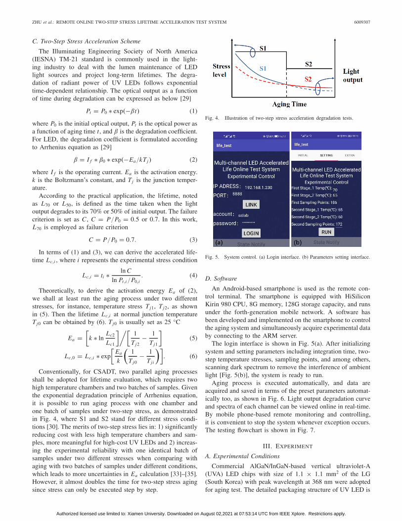
Conventionally, for CSADT, two parallel aging processesshall be adopted for lifetime evaluation, which requires twohigh temperature chambers and two batches of samples. Giventhe exponential degradation principle of Arrhenius equation,it is possible to run aging process with one chamber andone batch of samples under two-step stress, as demonstratedin Fig. 4, where S1 and S2 stand for different stress condi-tions [30]. The merits of two-step stress lies in: 1) significantlyreducing cost with less high temperature chambers and sam-ples, more meaningful for high-cost UV LEDs and 2) increas-ing the experimental reliability with one identical batch ofsamples under two different stresses when comparing withaging with two batches of samples under different conditions,which leads to more uncertainties in Ea calculation [33]–[35].However, it almost doubles the time for two-step stress agingsince stress can only be executed step by step.
Fig. 4. Illustration of two-step stress acceleration degradation tests.
Fig. 5. System control. (a) Login interface. (b) Parameters setting interface.
D. Software
An Android-based smartphone is used as the remote con-trol terminal. The smartphone is equipped with HiSiliconKirin 980 CPU, 8G memory, 128G storage capacity, and runsunder the forth-generation mobile network. A software hasbeen developed and implemented on the smartphone to controlthe aging system and simultaneously acquire experimental databy connecting to the ARM server.
The login interface is shown in Fig. 5(a). After initializingsystem and setting parameters including integration time, two-step temperature stresses, sampling points, and among others,scanning dark spectrum to remove the interference of ambientlight [Fig. 5(b)], the system is ready to run.
Aging process is executed automatically, and data areacquired and saved in terms of the preset parameters automat-ically too, as shown in Fig. 6. Light output degradation curveand spectra of each channel can be viewed online in real-time.By mobile phone-based remote monitoring and controlling,it is convenient to stop the system whenever exception occurs.The testing flowchart is shown in Fig. 7.
III. EXPERIMENT
A. Experimental Conditions
Commercial AlGaN/InGaN-based vertical ultraviolet-A(UVA) LED chips with size of 1.1 × 1.1 mm2 of the LG(South Korea) with peak wavelength at 368 nm were adoptedfor aging test. The detailed packaging structure of UV LED is
Authorized licensed use limited to: Xiamen University. Downloaded on August 02,2021 at 07:53:14 UTC from IEEE Xplore. Restrictions apply.

6009307 IEEE TRANSACTIONS ON INSTRUMENTATION AND MEASUREMENT, VOL. 70, 2021
Fig. 6. Data acquisition. (a) Irradiance as a function of aging time.(b) Spectral of UV LED.
Fig. 7. Testing flowchart of the system.
Fig. 8. Illustrations of the test sample. (a) Magnification of UV LED chip.(b) UV LED mounted on a copper heat sink.
show in Fig. 8(a). Sample is mounted on a hexagonal copperheat sink to boost heat dissipation, as shown in Fig. 8(b).
After 200 h of preaging, 10 UV LEDs samples are selectedand divided into two groups: Samples 1–5 as Group I and
TABLE I
EXPERIMENTAL CONDITIONS FOR UV LED AGING TEST
Fig. 9. Spectra before and after the calibration.
Samples 6–10 as Group II for two-step aging test, withexperimental conditions listed in Table I.
During the aging test, experimental data are recorded andsaved every 2 h automatically. Although one group is enoughto derive the activation energy Ea and lifetime of LED in termsof two-step stress aging theory, to further verify the reliabilityof two-step stress aging, two groups of two-step stress withdifferent temperature stresses are designed and compared inparallel.
B. Spectral Calibration
The calibration of the system is carried out before theexperiment to ensure the accuracy of results and sensitivityof the system [39] because the response of the spectrometerat each wavelength is inconsistent, also coupling betweenspectrometer and optical multiplexer will induce certain errors.A standard irradiance light source tested by Spectro320 spec-trometer (Instrument Systems) is used to calibrate the systemso that the relationship between the irradiance and the photoncounts is established. The detailed procedure of calibration canbe found in [36]. The calibration coefficients of each channelare imported to convert the photon counts into irradiancedistribution every time a spectrum is obtained. The comparisonbefore and after calibration for one channel is illustratedin Fig. 9.
C. Junction Temperature Measurement
The average junction temperature of LED is related withoptical parameters linearly, including peak wavelength [40],blue centroid wavelength of spectrum [41], and whiteblue ratio (W/B) [42]. In this work, the peak wave-length (λp) is selected as the temperature-sensitive opticalparameter (TSOP).
Prior to measuring the junction temperature of LED chip,the temperature-related coefficient is calibrated by a short
Authorized licensed use limited to: Xiamen University. Downloaded on August 02,2021 at 07:53:14 UTC from IEEE Xplore. Restrictions apply.

ZHU et al.: REMOTE ONLINE TWO-STEP STRESS LIFETIME ACCELERATION TEST SYSTEM 6009307
Fig. 10. Peak wavelength–junction temperature relationship.
Fig. 11. Light output degradation curves for (a) Group I and (b) Group IIunder two-step stress.
current pulse signal so as to remove the self-heating effect withthe heat sink temperature set from 35 ◦C to 75 ◦C with intervalof 10 ◦C. The linear fitting of peak wavelength with junctiontemperature relationships of all samples are shown in Fig. 10,where the symbols represent experimental data and straightlines represent fitting results. In the aging process, the real-time junction temperature can be derived from the measuredpeak wavelength.
IV. RESULTS AND DISCUSSION
A. Experimental Results
Fig. 11 shows the normalized light output degradationcurves under two-step stresses for five samples of eachgroup, respectively. A vertical line indicates the dividing timebetween the two steps. Sharper degradation trends observedin samples of Group II at Step I aging process might indicateexistence of samples differences between the two batches.Fig. 12 shows the spectra of sample 9 at the aging timeof 4, 180, 360, 540, and 720 h. From Fig. 12(b), the peakwavelength of samples almost keeps stable during each stepof aging, which in turn implies the stability of junctiontemperature.
B. Lifetime Calculation
The lifetime (L70) under each stress is derived by expo-nential fitting of the degradation curve (Fig. 11). Then theactivation energy (Ea) and lifetime at specific junction tem-perature (25 ◦C) can be calculated in terms of (5) and (6),as listed in Table II. The shorter lifetimes of Step I thanthose of Step II of each group, even at same temperature
Fig. 12. (a) Spectra and (b) peak wavelength shift during aging.
TABLE II
LIFETIME CALCULATION
stress (Group I Step 2 and Group II Step 1), might implyintrinsic characteristics of UV LEDs. Usually, LEDs undergo adrastic drop in light output during their initial aging stage whenthe preaging time is not long enough. This phenomenon hasbeen confirmed and reported by literatures [33], [34], probablyattributed to the defects and dislocation-related early failuremechanism. The average lifetime (Ave. L70) of two groupsof UV LEDs is 56 368 and 58 741 h, respectively. Resultsof both groups are generally in agreement, with about 4%relative error, suggesting feasibility and accuracy of two-stepstress method.
V. CONCLUSION
In this article, an online lifetime acceleration test systemcombined with ARM server and smartphone is developed tocontrol and monitor the lifetime acceleration of UV LEDsdynamically and remotely. Given the special safety require-ment of UV LED, a black UV shield is built to enclose thewhole UV LED fixture to prevent from UV radiation andleakage. The peak wavelength of UV emission is adoptedas a temperature-sensitive parameter to calculate junctiontemperature, by which the lifetime can be accurately derived.By applying two-step temperature stress, one batch of UVLEDs is enough to derive lifetime so that the cost can besignificantly reduced and the calculation of activation energyas well as lifetime are more reliable. Experimental resultsof UV LEDs demonstrate feasibility and accuracy of thismethod in this test system. The test system provides a valuabletool for evaluating the lifetime of UV LEDs safely, reliably,and accurately. Besides, acquired spectra during aging offerabundant information for future research, such as chromaticitystability, failure mechanism. Combining current stress with
Authorized licensed use limited to: Xiamen University. Downloaded on August 02,2021 at 07:53:14 UTC from IEEE Xplore. Restrictions apply.

6009307 IEEE TRANSACTIONS ON INSTRUMENTATION AND MEASUREMENT, VOL. 70, 2021
temperature stress, it is also possible to carry out compoundaccelerated degradation test in this system in the future.
REFERENCES
[1] P. Mukish and P. Boulay, “UV LEDS-technology, manufacturing andapplication trends,” Yole Développement, Lyon, France, Tech. Rep.,May 2018.
[2] A.-C. Chevremont, A.-M. Farnet, B. Coulomb, and J.-L. Boudenne,“Effect of coupled UV-A and UV-C LEDs on both microbiological andchemical pollution of urban wastewaters,” Sci. Total Environ., vol. 426,pp. 304–310, Jun. 2012.
[3] J. Chen, S. Loeb, and J.-H. Kim, “The LED revolution: The basicprinciples and prospects of UV disinfection application,” Environ. Sci.,Water Res. Technol., vol. 3, no. 2, pp. 188–202, 2017.
[4] P. O. Nyangaresi, Y. Qin, G. Chen, B. Zhang, Y. Lu, and L. Shen,“Comparison of the performance of pulsed and continuous UVC-LED irradiation in the inactivation of bacteria,” Water Res., vol. 157,pp. 218–227, Jun. 2019.
[5] Y. Yang, H. Zhang, S. S. Nunayon, V. Chan, and A. C. Lai, “Disinfectionefficacy of ultraviolet germicidal irradiation on airborne bacteria inventilation ducts,” Indoor Air, vol. 28, no. 6, pp. 806–817, Nov. 2018.
[6] K. C. Anyaogu, A. A. Ermoshkin, D. C. Neckers, A. Mejiritski,O. Grinevich, and A. V. Fedorov, “Performance of the light emittingdiodes versus conventional light sources in the UV light cured formu-lations,” J. Appl. Polym. Sci., vol. 105, no. 2, pp. 803–808, Jul. 2007.
[7] P. J. Hargis, T. J. Sobering, G. C. Tisone, J. S. Wagner, and R. J. Radloff,“Ultraviolet fuorescence detection and identifcation of protein,” DNABacteria, vol. 2366, pp. 147–153, Feb. 1995.
[8] M. Schreiner, J. M. Abaigar, J. Glaab, and M. Jansen, “UV-B inducedsecondary plant metabolites: Potential benefits for plant and humanhealth,” Opt. Photon., vol. 9, no. 2, pp. 34–37, 2014.
[9] J. Krutmann and A. Morita, “Mechanisms of ultraviolet (UV) B andUVA phototherapy,” J. Investigative Dermatol. Symp. Proc., vol. 4, no. 1,pp. 70–72, Sep. 1999.
[10] P. E. Hockberger, “A history of ultraviolet photobiology for humans,animals and microorganisms,” Photochem. Photobiol., vol. 76, no. 6,pp. 561–579, May 2007.
[11] M. Kneissl, T.-Y. Seong, J. Han, and H. Amano, “The emergence andprospects of deep-ultraviolet light-emitting diode technologies,” NaturePhoton., vol. 13, no. 4, pp. 233–244, Apr. 2019.
[12] H. Amano et al., “The 2020 UV emitter roadmap,” J. Phys. D, Appl.Phys., vol. 53, Sep. 2020, Art. no. 503001.
[13] Y. Li et al., “High-efficiency near-UV light-emitting diodes on Si sub-strates with InGaN/GaN/AlGaN/GaN multiple quantum wells,” J. Mater.Chem. C, vol. 27, Jan. 2020, Art. no. 115003.
[14] D. Wang, K. Uesugi, S. Xiao, K. Norimatsu, and H. Miyake, “High-quality AlN/sapphire templates prepared by thermal cycle annealing forhigh-performance ultraviolet light-emitting diodes,” Appl. Phys. Exp.,vol. 14, no. 3, Mar. 2021, Art. no. 035505.
[15] R. Ni et al., “AlGaN-based ultraviolet light-emitting diode on high-temperature annealed sputtered AlN template,” J. Alloys Compounds,vol. 794, pp. 8–12, Jul. 2019.
[16] T. H. Lee et al., “Smart wide-bandgap omnidirectional reflector as aneffective hole-injection electrode for deep-UV light-emitting diodes,”Adv. Opt. Mater., vol. 8, no. 2, Jan. 2020, Art. no. 1901430.
[17] T. Fudetani, K. Ueno, A. Kobayashi, and H. Fujioka, “Heavily Si-doped pulsed sputtering deposited GaN for tunneling junction contacts inUV-A light emitting diodes,” Appl. Phys. Lett., vol. 118, no. 7, Feb. 2021,Art. no. 072101.
[18] K.-B. Sim, S.-J. Yoon, H.-S. Im, and T.-Y. Seong, “Ag–Pd–Cu alloyreflector to improve the opto-electrical performance and electromigrationresistance of near ultraviolet GaN-based light-emitting diode,” J. AlloysCompounds, vol. 800, pp. 512–517, Sep. 2019.
[19] N. Zhang, F. Xu, J. Lang, L. Wang, and B. Shen, “Improved light extrac-tion efficiency of AlGaN deep-ultraviolet emitting diodes combining Ag-nanodots/Al reflective electrode with highly transparent p-type layer,”Opt. Exp., vol. 29, no. 2, pp. 2394–2401, Jan. 2021.
[20] G. Vincent et al., “UV emission from GaN wires with m-plane core–shell GaN/AlGaN multiple quantum wells,” ACS Appl. Mater. Interfaces,vol. 12, no. 39, pp. 44007–44016, Sep. 2020.
[21] J. Brault et al., “Internal quantum efficiencies of AlGaN quantum dotsgrown by molecular beam epitaxy and emitting in the UVA to UVCranges,” J. Appl. Phys., vol. 126, no. 20, Nov. 2019, Art. no. 205701.
[22] N. Gao et al., “Strain engineering of digitally alloyed AlN/GaN nanorodsfor far-UVC emission as short as 220 nm,” Opt. Mater. Exp., vol. 11,pp. 1282–1291, Apr. 2021.
[23] K. Kitamura, J. R. Grandusky, C. G. Moe, J. Chen, and L. J. Schowalter,“S3-P1: Reliability and lifetime of pseudomorphic UVC LEDs on AlNsubstrate under various stress condition,” in Proc. Lester Eastman Conf.High Perform. Devices (LEC), Ithaca, NY, USA, Aug. 2014, pp. 1–5.
[24] Z. Jing, J. Liu, M. S. Ibrahim, J. Fan, X. Fan, and G. Zhang, “Lifetimeprediction of ultraviolet light-emitting diodes using a long short-termmemory recurrent neural network,” IEEE Electron Device Lett., vol. 41,no. 12, pp. 1817–1820, Dec. 2020.
[25] A. Fujioka et al., “High-output-power 255/280/310 nm deep ultravioletlight-emitting diodes and their lifetime characteristics,” Semicond. Sci.Technol., vol. 29, no. 8, Aug. 2014, Art. no. 084005.
[26] J. Glaab et al., “Degradation of (InAlGa) N-based UV-B light emittingdiodes stressed by current and temperature,” J. Appl. Phys., vol. 201,no. 9, pp. 49–2717, Sep. 2015.
[27] J. Ruschel et al., “Current-induced degradation and lifetime predictionof 310 nm ultraviolet light-emitting diodes,” Photon. Res., vol. 7, no. 7,pp. 36–40, Jul. 2019.
[28] X.-X. Wang, L. Jing, Y. Wang, Q. Gao, and Q. Sun, “The influence ofjunction temperature variation of LED on the lifetime estimation duringaccelerated aging test,” IEEE Access, vol. 7, pp. 4773–4781, 2019.
[29] Projecting Long Term Lumen Maintenance of LED Light Sources,Standard TM-21-11, IESNA, 2011.
[30] E. M. Benavides, “Reliability model for step-stress and variable-stresssituations,” IEEE Trans. Rel., vol. 60, no. 1, pp. 219–233, Mar. 2011.
[31] W. Nelson, “Accelerated life testing-step-stress models and data analy-ses,” IEEE Trans. Reliab., vol. R-29, no. 2, pp. 103–108, Jun. 1980.
[32] J. Hao, D. Li, C. He, Q. Sun, and H. Ke, “Step-down accelerated agingtest for LED lamps based on Nelson models,” Optik, vol. 149, pp. 69–80,Nov. 2017.
[33] D. Yang, M. Cai, W. Chen, and Z. Zhang, “Fast life-time assessmentof LED luminaries,” in Proc. 2nd IEEE CPMT Symp. Jpn., Dec. 2012,pp. 1–4.
[34] J. Hao, Q. Sun, Z. Xu, L. Jing, Y. Wang, and H. L. Ke, “The designof two-step-down aging test for LED lamps under temperature stress,”IEEE Trans. Electron Device, vol. 63, no. 3, pp. 1–6, Mar. 2016.
[35] B. Liang et al., “Investigation of step-stress accelerated degradation teststrategy for ultraviolet light emitting diodes,” Materials, vol. 12, no. 19,p. 3119, Sep. 2019.
[36] J. Xiao et al., “Multichannel online lifetime accelerating and testingsystem for power light-emitting diode,” IEEE Photon. J., vol. 9, no. 3,Jun. 2017, Art. no. 820091.
[37] S. Zhou and S. Liu, “Transient measurement of light-emitting diodecharacteristic parameters for production lines,” Rev. Sci. Instrum.,vol. 80, no. 9, Sep. 2009, Art. no. 095102.
[38] P. Altieri-Weimar et al., “Influence of doping on the reliability ofAlGaInP LEDs,” J. Mater. Sci., Mater. Electron., vol. 19, no. S1,pp. 338–341, Dec. 2008.
[39] P. Fiorentin and A. Scroccaro, “Detector-based calibration for illu-minance and luminance meters—Experimental results,” IEEE Trans.Instrum. Meas., vol. 59, no. 5, pp. 1375–1381, May 2010.
[40] E. M. Sa, F. L. M. Antunes, and A. J. Perin, “Junction temperatureestimation for high power light-emitting diodes,” in Proc. IEEE Int.Symp. Ind. Electron., Jun. 2007, pp. 3030–3035.
[41] J. Jin et al., “A microscopic hyperspectral-based centroid wavelengthmethod for measuring two-dimensional junction temperature distributionof LEDs,” IEEE Electron Device Lett., vol. 40, no. 4, pp. 506–509,Apr. 2019.
[42] S. Chhajed, Y. Xi, Y. L. Li, T. Gessmann, and E. F. Schubert, “Influenceof junction temperature on chromaticity and color-rendering propertiesof trichromatic white-light sources based on light-emitting diodes,”J. Appl. Phys., vol. 97, pp. 1–8, Mar. 2005.
Li-Hong Zhu received the Ph.D. degree in micro-electronics and solid-state electronics from XiamenUniversity, Xiamen, China, in 2010.
Since 2013, she has been a Senior Engineer withthe Department of Electronic Science, Xiamen Uni-versity. Her research interests include the III-nitride-based light-emitting diodes materials and devices.
Authorized licensed use limited to: Xiamen University. Downloaded on August 02,2021 at 07:53:14 UTC from IEEE Xplore. Restrictions apply.

ZHU et al.: REMOTE ONLINE TWO-STEP STRESS LIFETIME ACCELERATION TEST SYSTEM 6009307
Qiu-Wei Zheng received the B.S. degree inelectronic information engineering from the CivilAviation University of China, Tianjin, China,in 2018. He is currently pursuing the M.S. degreewith the Department of Electronic Science, XiamenUniversity, Xiamen, China.
His research interests focus on semiconductorlighting and testing.
Yu-Jiao Ruan received the Ph.D. degree in micro-electronics and solid-state electronics from XiamenUniversity, Xiamen, China, in 2013.
She is currently a Senior Engineer with theXiamen Institute of Measurement and Testing. Herresearch interests include optical metrology andtesting.
Wei-Jie Guo received the Ph.D. degree in physicalelectronics from Xiamen University, Xiamen, China,in 2019.
Since 2020, he has been an Assistant Professorwith the Department of Electronic Science, Xia-men University. His research interests include theIII-nitride-based devices and light-emitting diodedisplays.
Yu-Lin Gao received the Ph.D. degree in condensedmatter physics from Xiamen University, Xiamen,China, in 2002.
Since 2011, she has been with the Department ofElectronic Science, Xiamen University, where she iscurrently an Associate Professor.
Zi-Quan Guo, photograph and biography not available at the time ofpublication.
Yue Lin received the B.S. degree in applied physicsfrom Southeast University, Nanjing, China, in 2007,and the Ph.D. degree in radio physics from XiamenUniversity, Xiamen, China, in 2012.
He is currently an Associate Professor withthe Department of Electronics Science, XiamenUniversity.
Ting-Zhu Wu received the B.S. degree from Zhe-jiang University, Hangzhou, China, in 2007, the M.S.degree from the Hong Kong University of Scienceand Technology, Hong Kong, China, in 2008, andthe Ph.D. degree from Xiamen University, Xiamen,China, in 2017.
He is currently an Associate Professor withthe Department of Electronic Science, XiamenUniversity.
Zhong Chen received the Ph.D. degree from Xia-men University, Xiamen, China, in 1993.
Since 2000, he has been a Professor with theDepartment of Physics and Department of Elec-tronic Science, Xiamen University, respectively. Hisresearch interests focus on scientific instrumentdesign and nuclear magnetic resonance.
Yi-Jun Lu received the Ph.D. degree in condensedmatter physics from Xiamen University, Xiamen,China, in 2000.
He was with the Department of Physics, XiamenUniversity, till 2011. Since then, he has been with theDepartment of Electronic Science, Xiamen Univer-sity, where he is currently a Professor. His researchinterests focus on Solid-state Lighting testing andapplication.
Authorized licensed use limited to: Xiamen University. Downloaded on August 02,2021 at 07:53:14 UTC from IEEE Xplore. Restrictions apply.