Reliability of Highly Stable Amorphous-Silicon Thin-Film ...
8
IEEE TRANSACTIONS ON DEVICE AND MATERIALS RELIABILITY, VOL. 16, NO. 2, JUNE 2016 255 Reliability of Highly Stable Amorphous-Silicon Thin-Film Transistors Under Low Gate-Field Stress—Part II: Optimization of Fabrication Conditions and Gate Voltage Dependence Ting Liu, Levent E. Aygun, Sigurd Wagner, Fellow, IEEE, and James C. Sturm, Fellow, IEEE Abstract—Part I of this paper introduced a two-stage model for reliability characterization and lifetime prediction of amorphous- silicon thin-film transistors (a-Si TFTs) under low gate-field stress that includes both charge trapping in the silicon nitride (SiN x ) gate dielectric and defect generation in the a-Si channel. In part II, the model is used to experimentally reduce the drain cur- rent instability under room temperature operation of a-Si TFTs under a prolonged gate bias of 5 V. Deposition conditions for the SiN x gate insulator and the a-Si channel layer were varied, and TFTs were fabricated with all reactive-ion-etch steps, or with all wet-etch steps. The stability of the a-Si channel also depends on the deposition conditions for the underlying SiN x gate insulator, and TFTs made with wet etching are more stable than TFTs made with reactive ion etching. Combining the various improvements raised the extrapolated 50% lifetime of the drain current of back- channel-passivated dry-etched TFTs under continuous operation in saturation at 20 ◦ C with V GS = 5 V from 3 × 10 4 s (9.2 h) to 4 × 10 7 s (1.4 years). We also extend the model, so that parameters from the degradation at one gate voltage can be used to estimate the degradation at other low gate voltages. Index Terms—Stability, a-Si TFTs, two-stage model, charge- trapping, defect-generation. I. I NTRODUCTION H YDROGENATED amorphous silicon thin-film transis- tors (a-Si:H TFTs) have been widely used as digital switches for the low-duty-cycle active-matrix addressing of liq- uid crystal displays, optical scanners and sensors [1], [2] since their first demonstration in 1976 [3]. Extending to their use in continuous operation, such as for pixel current sources in ac- tive matrix organic light emitting diode displays (AMOLEDs) where brightness is proportional to the TFT current, makes stability a critical issue. Stable current is also important in X-ray image sensors. Thus a stable threshold is critical [4]. Low power dissipation while operating in saturation also requires a Manuscript received July 1, 2015; revised December 28, 2015; accepted January 8, 2016. Date of publication February 5, 2016; date of current version June 3, 2016. This work was supported in part by the Princeton Program in Plasma Science and Technology (DoE DE-AC02-09CH11466), in part by the National Science Foundation (ECCS-1202168), in part by the Air Force Office of Scientific Research (FA9550-12-1-0200), in part by the Department of Energy (Energy Efficiency Buildings HUB, DE-EE0004261), and in part by the Industrial Technology Research Institute, Taiwan (ITRI). The authors are with the Department of Electrical Engineering and Princeton Institute for the Science and Technology of Materials (PRISM), Princeton University, Princeton, NJ 08544 USA (e-mail: [email protected]). Digital Object Identifier 10.1109/TDMR.2016.2524626 low gate voltage (5 V). At low gate bias a different physical mechanism (a-Si defect generation) is the dominant cause of threshold voltage shift (part I of this paper and [2], [5], [6]) in- stead of charge trapping in the gate dielectric, which is thought to dominate at much higher gate voltages such as those used in Active matrix liquid-crystal display (AMLCD) circuits. In Part II of the paper, a systematic experimental study to optimize a-Si stability for low-voltage (5 V V GS ) operation at room temperature is presented. We varied both deposition conditions and etching methods, and linked their effects with the physical mechanisms that change the threshold voltage of a-Si TFTs under low gate bias. The a-Si TFT stability depends on their fabrication processes, in particular a-Si and SiN x depo- sition conditions and etching methods. Among the deposition conditions, hydrogen dilution [7], [8] and ammonia to silane flow ratio for SiN x gate insulator growth [8], [9], SiN x deposi- tion temperature [7]–[9], a-Si deposition temperature [10], [11] and hydrogen dilution [5], [6], [10] for a-Si growth have been shown to affect the stability of a-Si TFTs. Wet-etched a-Si TFTs [12] have been reported to be more stable than dry-etched TFTs. In Part I of this paper, we presented a two-stage model for characterizing stability and predicting the saturation mode lifetime of highly stable a-Si TFTs under low gate-field stress (∼ 1.5 × 10 5 V/cm, 5 V V GS for 300-nm-thick SiN x ). The drain current degradation can be modeled as an effective total threshold voltage shift ΔV T,eff,total (t), where all the change in drain current was attributed to the threshold voltage change I D (t)= μ n C ins W 2L [V GS − (V T 0 +ΔV T,eff,total (t))] 2 . (1) The “effective” threshold voltage terminology is used because the devices are in saturation (Part I, Sect. C.2). Our experiments showed that even with accelerated tests up to 160 ◦ C, with the current decreasing to as low 14% of its original value [13], the mobility changed by less than 10%, justifying modeling the current degradation as an effective threshold voltage increase. The effective threshold voltage shift ΔV T,eff,total (t) of a-Si TFTs develops in two stages: the fast ini- tial threshold voltage shift ΔV T,eff ,I (t) (Stage I), and the dom- inant long-term threshold voltage shift ΔV T,eff ,II (t) (Stage II) ΔV T,eff,total (t)=ΔV T,eff ,I (t)+ΔV T,eff,II (t). (2) 1530-4388 © 2016 IEEE. Personal use is permitted, but republication/redistribution requires IEEE permission. See http://www.ieee.org/publications_standards/publications/rights/index.html for more information.
Transcript of Reliability of Highly Stable Amorphous-Silicon Thin-Film ...
IEEE TRANSACTIONS ON DEVICE AND MATERIALS RELIABILITY, VOL. 16, NO. 2, JUNE 2016 255
Reliability of Highly Stable Amorphous-SiliconThin-Film Transistors Under Low Gate-FieldStress—Part II: Optimization of FabricationConditions and Gate Voltage Dependence
Ting Liu, Levent E. Aygun, Sigurd Wagner, Fellow, IEEE, and James C. Sturm, Fellow, IEEE
Abstract—Part I of this paper introduced a two-stage model forreliability characterization and lifetime prediction of amorphous-silicon thin-film transistors (a-Si TFTs) under low gate-field stressthat includes both charge trapping in the silicon nitride (SiNx)gate dielectric and defect generation in the a-Si channel. Inpart II, the model is used to experimentally reduce the drain cur-rent instability under room temperature operation of a-Si TFTsunder a prolonged gate bias of 5 V. Deposition conditions for theSiNx gate insulator and the a-Si channel layer were varied, andTFTs were fabricated with all reactive-ion-etch steps, or with allwet-etch steps. The stability of the a-Si channel also depends onthe deposition conditions for the underlying SiNx gate insulator,and TFTs made with wet etching are more stable than TFTs madewith reactive ion etching. Combining the various improvementsraised the extrapolated 50% lifetime of the drain current of back-channel-passivated dry-etched TFTs under continuous operationin saturation at 20 ◦C with VGS = 5 V from 3 × 10⁴ s (9.2 h) to4 × 107 s (1.4 years). We also extend the model, so that parametersfrom the degradation at one gate voltage can be used to estimatethe degradation at other low gate voltages.
Index Terms—Stability, a-Si TFTs, two-stage model, charge-trapping, defect-generation.
I. INTRODUCTION
HYDROGENATED amorphous silicon thin-film transis-tors (a-Si:H TFTs) have been widely used as digital
switches for the low-duty-cycle active-matrix addressing of liq-uid crystal displays, optical scanners and sensors [1], [2] sincetheir first demonstration in 1976 [3]. Extending to their use incontinuous operation, such as for pixel current sources in ac-tive matrix organic light emitting diode displays (AMOLEDs)where brightness is proportional to the TFT current, makesstability a critical issue. Stable current is also important inX-ray image sensors. Thus a stable threshold is critical [4]. Lowpower dissipation while operating in saturation also requires a
Manuscript received July 1, 2015; revised December 28, 2015; acceptedJanuary 8, 2016. Date of publication February 5, 2016; date of current versionJune 3, 2016. This work was supported in part by the Princeton Programin Plasma Science and Technology (DoE DE-AC02-09CH11466), in part bythe National Science Foundation (ECCS-1202168), in part by the Air ForceOffice of Scientific Research (FA9550-12-1-0200), in part by the Departmentof Energy (Energy Efficiency Buildings HUB, DE-EE0004261), and in part bythe Industrial Technology Research Institute, Taiwan (ITRI).
The authors are with the Department of Electrical Engineering and PrincetonInstitute for the Science and Technology of Materials (PRISM), PrincetonUniversity, Princeton, NJ 08544 USA (e-mail: [email protected]).
Digital Object Identifier 10.1109/TDMR.2016.2524626
low gate voltage (�5 V). At low gate bias a different physicalmechanism (a-Si defect generation) is the dominant cause ofthreshold voltage shift (part I of this paper and [2], [5], [6]) in-stead of charge trapping in the gate dielectric, which is thoughtto dominate at much higher gate voltages such as those used inActive matrix liquid-crystal display (AMLCD) circuits.
In Part II of the paper, a systematic experimental study tooptimize a-Si stability for low-voltage (5 V VGS) operationat room temperature is presented. We varied both depositionconditions and etching methods, and linked their effects withthe physical mechanisms that change the threshold voltage ofa-Si TFTs under low gate bias. The a-Si TFT stability dependson their fabrication processes, in particular a-Si and SiNx depo-sition conditions and etching methods. Among the depositionconditions, hydrogen dilution [7], [8] and ammonia to silaneflow ratio for SiNx gate insulator growth [8], [9], SiNx deposi-tion temperature [7]–[9], a-Si deposition temperature [10], [11]and hydrogen dilution [5], [6], [10] for a-Si growth have beenshown to affect the stability of a-Si TFTs. Wet-etched a-Si TFTs[12] have been reported to be more stable than dry-etched TFTs.
In Part I of this paper, we presented a two-stage modelfor characterizing stability and predicting the saturation modelifetime of highly stable a-Si TFTs under low gate-field stress(∼1.5 × 10⁵ V/cm, 5 V VGS for 300-nm-thick SiNx). Thedrain current degradation can be modeled as an effective totalthreshold voltage shift ΔVT,eff,total(t), where all the change indrain current was attributed to the threshold voltage change
ID(t) = μnCinsW
2L[VGS − (VT0 +ΔVT,eff,total(t))]
2 . (1)
The “effective” threshold voltage terminology is used becausethe devices are in saturation (Part I, Sect. C.2).
Our experiments showed that even with accelerated tests upto 160 ◦C, with the current decreasing to as low 14% of itsoriginal value [13], the mobility changed by less than 10%,justifying modeling the current degradation as an effectivethreshold voltage increase. The effective threshold voltage shiftΔVT,eff,total(t)of a-Si TFTs develops in two stages: the fast ini-tial threshold voltage shift ΔVT,eff,I(t) (Stage I), and the dom-inant long-term threshold voltage shift ΔVT,eff,II(t) (Stage II)
ΔVT,eff,total(t) = ΔVT,eff,I(t) + ΔVT,eff,II(t). (2)
1530-4388 © 2016 IEEE. Personal use is permitted, but republication/redistribution requires IEEE permission.See http://www.ieee.org/publications_standards/publications/rights/index.html for more information.
256 IEEE TRANSACTIONS ON DEVICE AND MATERIALS RELIABILITY, VOL. 16, NO. 2, JUNE 2016
The threshold voltage shift in Stage I is most likely causedby charge trapping in SiNx. It can be modeled with a stretchedexponential model
ΔVT,eff,I(t) = ΔVT,eff,max,I
{1 − exp
[−(
1t0,eff,I
)βI
]}.
(3)The threshold voltage shift in Stage II, ΔVT,eff,II(t), is
caused by defect creation in a-Si also fits a stretched exponen-tial expression
ΔVT,eff,II(t) = (VGS − VT0 −ΔVT,eff,max,I)
×{1− exp
[−(
t
t0,eff,II
)βII
]}(4)
where
βII =T
T0(5)
t0,eff,II = v−1 exp
(Eact,eff
kT
)(6)
or, in terms of fundamental parameters
t0,eff,II = v−1
(nch,o
C0kT0
)T0T
(7)
where v is an attempt frequency,T0 is the characteristic temper-ature reflecting the weak bond distribution in energy, Eact,eff,II
is an effective activation energy of the defect creation, C0 isthe pre-exponential constant in the distribution of weak bondsversus bond strength, and nch,o is a constant inversely reflectingthe sensitivity of the bond breaking rate of electron density. Wenow go on to use the model to optimize process conditions forlong-term reliability near room temperature.
II. FABRICATION OF A-SI TFTS
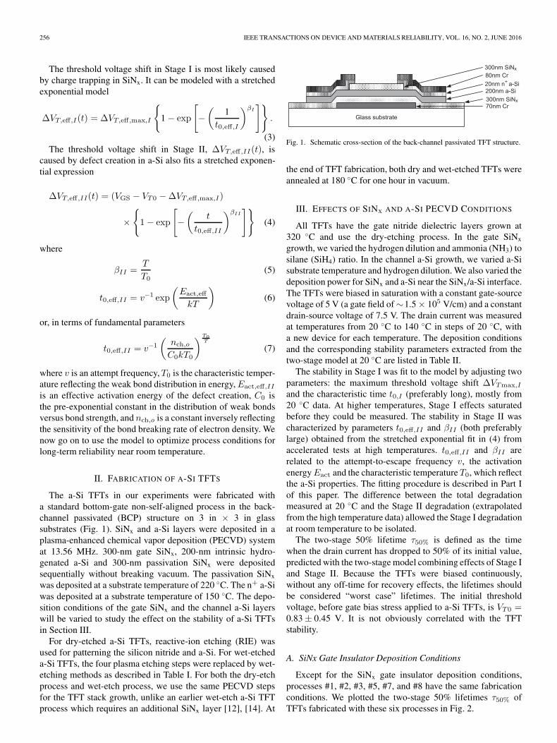
The a-Si TFTs in our experiments were fabricated witha standard bottom-gate non-self-aligned process in the back-channel passivated (BCP) structure on 3 in × 3 in glasssubstrates (Fig. 1). SiNx and a-Si layers were deposited in aplasma-enhanced chemical vapor deposition (PECVD) systemat 13.56 MHz. 300-nm gate SiNx, 200-nm intrinsic hydro-genated a-Si and 300-nm passivation SiNx were depositedsequentially without breaking vacuum. The passivation SiNx
was deposited at a substrate temperature of 220 ◦C. The n+ a-Siwas deposited at a substrate temperature of 150 ◦C. The depo-sition conditions of the gate SiNx and the channel a-Si layerswill be varied to study the effect on the stability of a-Si TFTsin Section III.
For dry-etched a-Si TFTs, reactive-ion etching (RIE) wasused for patterning the silicon nitride and a-Si. For wet-etcheda-Si TFTs, the four plasma etching steps were replaced by wet-etching methods as described in Table I. For both the dry-etchprocess and wet-etch process, we use the same PECVD stepsfor the TFT stack growth, unlike an earlier wet-etch a-Si TFTprocess which requires an additional SiNx layer [12], [14]. At
Fig. 1. Schematic cross-section of the back-channel passivated TFT structure.
the end of TFT fabrication, both dry and wet-etched TFTs wereannealed at 180 ◦C for one hour in vacuum.
III. EFFECTS OF SINX AND A-SI PECVD CONDITIONS
All TFTs have the gate nitride dielectric layers grown at320 ◦C and use the dry-etching process. In the gate SiNx
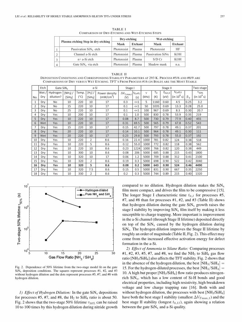
growth, we varied the hydrogen dilution and ammonia (NH3) tosilane (SiH4) ratio. In the channel a-Si growth, we varied a-Sisubstrate temperature and hydrogen dilution. We also varied thedeposition power for SiNx and a-Si near the SiNx/a-Si interface.The TFTs were biased in saturation with a constant gate-sourcevoltage of 5 V (a gate field of ∼1.5 × 10⁵ V/cm) and a constantdrain-source voltage of 7.5 V. The drain current was measuredat temperatures from 20 ◦C to 140 ◦C in steps of 20 ◦C, witha new device for each temperature. The deposition conditionsand the corresponding stability parameters extracted from thetwo-stage model at 20 ◦C are listed in Table II.
The stability in Stage I was fit to the model by adjusting twoparameters: the maximum threshold voltage shift ΔVTmax,I
and the characteristic time t0,I (preferably long), mostly from20 ◦C data. At higher temperatures, Stage I effects saturatedbefore they could be measured. The stability in Stage II wascharacterized by parameters t0,eff,II and βII (both preferablylarge) obtained from the stretched exponential fit in (4) fromaccelerated tests at high temperatures. t0,eff,II and βII arerelated to the attempt-to-escape frequency v, the activationenergyEact and the characteristic temperatureT0, which reflectthe a-Si properties. The fitting procedure is described in Part Iof this paper. The difference between the total degradationmeasured at 20 ◦C and the Stage II degradation (extrapolatedfrom the high temperature data) allowed the Stage I degradationat room temperature to be isolated.
The two-stage 50% lifetime τ50% is defined as the timewhen the drain current has dropped to 50% of its initial value,predicted with the two-stage model combining effects of Stage Iand Stage II. Because the TFTs were biased continuously,without any off-time for recovery effects, the lifetimes shouldbe considered “worst case” lifetimes. The initial thresholdvoltage, before gate bias stress applied to a-Si TFTs, is VT0 =0.83 ± 0.45 V. It is not obviously correlated with the TFTstability.
A. SiNx Gate Insulator Deposition Conditions
Except for the SiNx gate insulator deposition conditions,processes #1, #2, #3, #5, #7, and #8 have the same fabricationconditions. We plotted the two-stage 50% lifetimes τ50% ofTFTs fabricated with these six processes in Fig. 2.
LIU et al.: RELIABILITY OF HIGHLY STABLE AMORPHOUS-SILICON TFTs UNDER STRESS 257
TABLE ICOMPARISON OF DRY-ETCHING AND WET-ETCHING STEPS
TABLE IIDEPOSITION CONDITIONS AND CORRESPONDING STABILITY PARAMETERS AT 293 K. PROCESS #5/6 AND #8/9 ARE
COMPARISONS OF DRY VERSUS WET ETCHING. TFT’S FROM PROCESS #16 (IN BOLD) ARE THE MOST STABLE
Fig. 2. Dependence of 50% lifetime from the two-stage model fit on the gateSiNx deposition conditions. The squares represent processes #1, #2, and #3without hydrogen dilution and the dots represent processes #5, #7, and #8 withhydrogen dilution.
1) Effect of Hydrogen Dilution: In the gate SiNx depositionsfor processes #5, #7, and #8, the H2 to SiH4 ratio is about 50.Fig. 2 shows that the two-stage 50% lifetime τ50% can be raised10 to 100 times by this hydrogen dilution during nitride growth
compared to no dilution. Hydrogen dilution makes the SiNx
film more compact, and drives the film to be compressive [15].The longer Stage I characteristic time t0,I for processes #5,#7, and #8 than for processes #1, #2, and #3 (Table II) showsthat hydrogen dilution during the gate SiNx growth raises thestage I stability by improving SiNx film itself by making it lesssusceptible to charge trapping. More important is improvementin the a-Si channel (through Stage II lifetime) deposited directlyon top of the SiNx caused by the hydrogen dilution duringSiNx. The hydrogen dilution improves the Stage II lifetime byroughly an order of magnitude (Table II, Fig. 2). This effect maycome from the increased effective activation energy for defectformation in the a-Si.
2) Effect of Ammonia to Silane Ratio: Comparing processes#1, #2, #3, #5, #7, and #8, we find the NH3 to SiH4 gas flowratio [NH3/SiH4] also affects the TFT stability. Fig. 2 shows thatin the absence of the hydrogen dilution, the best [NH3/SiH4] =15. For the hydrogen-diluted processes, the best [NH3/SiH4] =10. A high but proper [NH3/SiH4] flow ratio produces nitrogen-rich SiNx, which has a low content of Si-H bonds and goodelectrical properties, including high resistivity, high breakdownvoltage and low charge trapping rate [16]. Both with andwithout hydrogen dilution, the processes with best [NH3/SiH4]have both the best stage I stability (smallest ΔVTmax,1) and thebest stage II stability (longest t0,II ), again showing a relationbetween the gate SiNx and a-Si quality.
258 IEEE TRANSACTIONS ON DEVICE AND MATERIALS RELIABILITY, VOL. 16, NO. 2, JUNE 2016
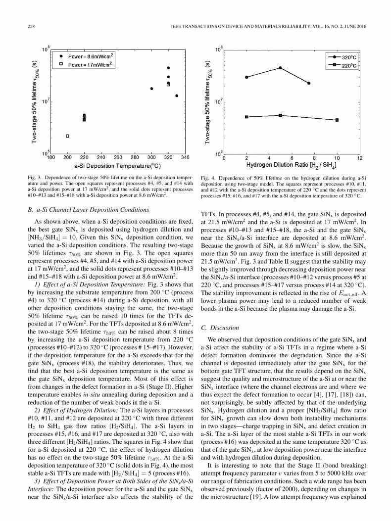
Fig. 3. Dependence of two-stage 50% lifetime on the a-Si deposition temper-ature and power. The open squares represent processes #4, #5, and #14 witha-Si deposition power at 17 mW/cm2, and the solid dots represent processes#10–#13 and #15–#18 with a-Si deposition power at 8.6 mW/cm2.
B. a-Si Channel Layer Deposition Conditions
As shown above, when a-Si deposition conditions are fixed,the best gate SiNx is deposited using hydrogen dilution and[NH3/SiH4] = 10. Given this SiNx deposition condition, wevaried the a-Si deposition conditions. The resulting two-stage50% lifetimes τ50% are shown in Fig. 3. The open squaresrepresent processes #4, #5, and #14 with a-Si deposition powerat 17 mW/cm2, and the solid dots represent processes #10–#13and #15–#18 with a-Si deposition power at 8.6 mW/cm2.
1) Effect of a-Si Deposition Temperature: Fig. 3 shows thatby increasing the substrate temperature from 200 ◦C (process#4) to 320 ◦C (process #14) during a-Si deposition, with allother deposition conditions staying the same, the two-stage50% lifetime τ50% can be raised 10 times for the TFTs de-posited at 17 mW/cm2. For the TFTs deposited at 8.6 mW/cm2,the two-stage 50% lifetime τ50% can be raised about 8 timesby increasing the a-Si deposition temperature from 220 ◦C(processes #10–#12) to 320 ◦C (processes # 15–#17). However,if the deposition temperature for the a-Si exceeds that for thegate SiNx (process #18), the stability deteriorates. Thus, wefind that the best a-Si deposition temperature is the same asthe gate SiNx deposition temperature. Most of this effect isfrom changes in the defect formation in a-Si (Stage II). Highertemperature enables in-situ annealing during deposition and areduction of the number of weak bonds in the a-Si.
2) Effect of Hydrogen Dilution: The a-Si layers in processes#10, #11, and #12 are deposited at 220 ◦C with three differentH2 to SiH4 gas flow ratios [H2/SiH4]. The a-Si layers inprocesses #15, #16, and #17 are deposited at 320 ◦C, also withthree different [H2/SiH4] ratios. The squares in Fig. 4 show thatfor a-Si deposited at 220 ◦C, the effect of hydrogen dilutionhas no effect on the two-stage 50% lifetime τ50%. At the a-Sideposition temperature of 320 ◦C (solid dots in Fig. 4), the moststable a-Si TFTs are made with [H2/SiH4] = 5 (process #16).
3) Effect of Deposition Power at Both Sides of the SiNx/a-SiInterface: The deposition power for the a-Si and the gate SiNx
near the SiNx/a-Si interface also affects the stability of the
Fig. 4. Dependence of 50% lifetime on the hydrogen dilution during a-Sideposition using two-stage model. The squares represent processes #10, #11,and #12 with the a-Si deposition temperature of 220 ◦C and the dots representprocesses #15, #16, and #17 with the a-Si deposition temperature of 320 ◦C.
TFTs. In processes #4, #5, and #14, the gate SiNx is depositedat 21.5 mW/cm2 and the a-Si is deposited at 17 mW/cm2. Inprocesses #10–#13 and #15–#18, the a-Si and the gate SiNx
near the SiNx/a-Si interface are deposited at 8.6 mW/cm2.Because the growth of SiNx at 8.6 mW/cm2 is slow, the SiNx
more than 50 nm away from the interface is still deposited at21.5 mW/cm2. Fig. 3 and Table II suggest that the stability maybe slightly improved through decreasing deposition power nearthe SiNx/a-Si interface (processes #10–#12 versus process #5 at220 ◦C, and processes #15–#17 versus process #14 at 320 ◦C).The stability improvement is reflected in the rise of Eact,eff . Alower plasma power may lead to a reduced number of weakbonds in the a-Si because the plasma may damage the a-Si.
C. Discussion
We observed that deposition conditions of the gate SiNx anda-Si affect the stability of a-Si TFTs in a regime where a-Sidefect formation dominates the degradation. Since the a-Sichannel is deposited immediately after the gate SiNx for thebottom gate TFT structure, that the results depend on the SiNx
suggest the quality and microstructure of the a-Si at or near theSiNx interface (where the channel electrons are and where wethus expect the defect formation to occur [4], [17], [18]) can,not surprisingly, be subtly affected by that of the underlyingSiNx. Hydrogen dilution and a proper [NH3/SiH4] flow ratiofor SiNx growth can slow down both instability mechanismsin two stages—charge trapping in SiNx and defect creation ina-Si. The a-Si layer of the most stable a-Si TFTs in our work(process #16) was deposited at the same temperature 320 ◦C asthat of the gate SiNx, at low deposition power near the interfaceand with hydrogen dilution during deposition.
It is interesting to note that the Stage II (bond breaking)attempt frequency parameter v varies from 5 to 5000 kHz overour range of fabrication conditions. Such a wide range has beenobserved previously (factor of 2000), depending on changes inthe microstructure [19]. A low attempt frequency was explained
LIU et al.: RELIABILITY OF HIGHLY STABLE AMORPHOUS-SILICON TFTs UNDER STRESS 259
as having resulted from regions having weak bonds (likely tobreak) having a small number of electrons, which accelerate thedefect-formation process. This implies the electron density maynot be uniform on a microscopic level in samples with low ν.
There was no single parameter which was key to highStage II stability, but rather their combination is important.High T0 implies that the number of bonds does not rapidlyincrease as bond strength is increased—a low number of weakbonds and thus high T0 is desirable. Also, important is a lowpre-exponential constant C0 in the distribution of bonds versusbond strength and a large nch,o, which inversely reflects thesensitivity of bond breaking to electron density (see (7) fort0,eff,II above, and (6) and (8) in Part I). In modeling, thesedependences are reflected through the activation energy of thecharacteristic time t0,eff,II parameter in Stage II, Eact,eff,II
Eact,eff,II = kT ln(vt0,eff,II)
= kT0 ln
(nch,o
C0kT0
). (8)
Thus, a high Eact,eff is desirable. Also, note that outside itsdependence on Eact,eff,II , there is no dependence of t0,eff,IIon T0 or any other physical parameter other than the escapefrequency.
Repeating (34) in Part I of this paper, the time τx%,II for thedrain current to decrease to x percent of its original value instage II is
τx%,II =
(− ln(x%)
2
)T0T
t0,eff,II
=
(1v
)(− ln(x%)
2
)T0T
eEAct,eff,II
kT . (9)
(9) summarizes that for a high lifetime, a high EAct,eff,II iscrucial. Outside of the exponential dependence on EAct,eff,II ,the dependence of lifetime on T0 is only modest. This isreflected experimentally in the fact that in Table II our moststable process (#16) has a relatively low T0 but the highestEAct,eff,II .
IV. STABILITY OF WET VERSUS DRY-ETCHED TFTS
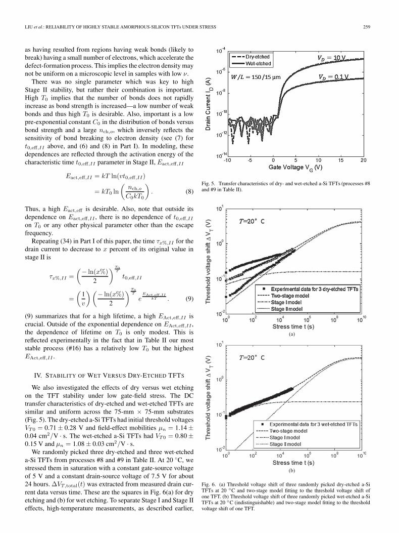
We also investigated the effects of dry versus wet etchingon the TFT stability under low gate-field stress. The DCtransfer characteristics of dry-etched and wet-etched TFTs aresimilar and uniform across the 75-mm × 75-mm substrates(Fig. 5). The dry-etched a-Si TFTs had initial threshold voltagesVT0 = 0.71 ± 0.28 V and field-effect mobilities μn = 1.14 ±0.04 cm2/V · s. The wet-etched a-Si TFTs had VT0 = 0.80 ±0.15 V and μn = 1.08 ± 0.03 cm2/V · s.
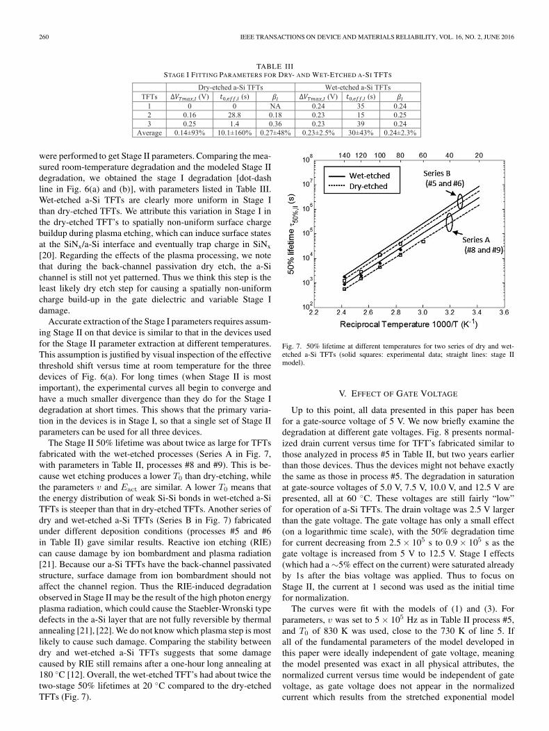
We randomly picked three dry-etched and three wet-etcheda-Si TFTs from processes #8 and #9 in Table II. At 20 ◦C, westressed them in saturation with a constant gate-source voltageof 5 V and a constant drain-source voltage of 7.5 V for about24 hours. ΔVT,total(t) was extracted from measured drain cur-rent data versus time. These are the squares in Fig. 6(a) for dryetching and (b) for wet etching. To separate Stage I and Stage IIeffects, high-temperature measurements, as described earlier,
Fig. 5. Transfer characteristics of dry- and wet-etched a-Si TFTs (processes #8and #9 in Table II).
Fig. 6. (a) Threshold voltage shift of three randomly picked dry-etched a-SiTFTs at 20 ◦C and two-stage model fitting to the threshold voltage shift ofone TFT. (b) Threshold voltage shift of three randomly picked wet-etched a-SiTFTs at 20 ◦C (indistinguishable) and two-stage model fitting to the thresholdvoltage shift of one TFT.
260 IEEE TRANSACTIONS ON DEVICE AND MATERIALS RELIABILITY, VOL. 16, NO. 2, JUNE 2016
TABLE IIISTAGE I FITTING PARAMETERS FOR DRY- AND WET-ETCHED A-SI TFTS
were performed to get Stage II parameters. Comparing the mea-sured room-temperature degradation and the modeled Stage IIdegradation, we obtained the stage I degradation [dot-dashline in Fig. 6(a) and (b)], with parameters listed in Table III.Wet-etched a-Si TFTs are clearly more uniform in Stage Ithan dry-etched TFTs. We attribute this variation in Stage I inthe dry-etched TFT’s to spatially non-uniform surface chargebuildup during plasma etching, which can induce surface statesat the SiNx/a-Si interface and eventually trap charge in SiNx
[20]. Regarding the effects of the plasma processing, we notethat during the back-channel passivation dry etch, the a-Sichannel is still not yet patterned. Thus we think this step is theleast likely dry etch step for causing a spatially non-uniformcharge build-up in the gate dielectric and variable Stage Idamage.
Accurate extraction of the Stage I parameters requires assum-ing Stage II on that device is similar to that in the devices usedfor the Stage II parameter extraction at different temperatures.This assumption is justified by visual inspection of the effectivethreshold shift versus time at room temperature for the threedevices of Fig. 6(a). For long times (when Stage II is mostimportant), the experimental curves all begin to converge andhave a much smaller divergence than they do for the Stage Idegradation at short times. This shows that the primary varia-tion in the devices is in Stage I, so that a single set of Stage IIparameters can be used for all three devices.
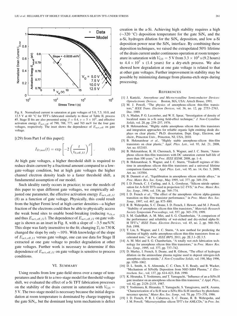
The Stage II 50% lifetime was about twice as large for TFTsfabricated with the wet-etched processes (Series A in Fig. 7,with parameters in Table II, processes #8 and #9). This is be-cause wet etching produces a lower T0 than dry-etching, whilethe parameters v and Eact are similar. A lower T0 means thatthe energy distribution of weak Si-Si bonds in wet-etched a-SiTFTs is steeper than that in dry-etched TFTs. Another series ofdry and wet-etched a-Si TFTs (Series B in Fig. 7) fabricatedunder different deposition conditions (processes #5 and #6in Table II) gave similar results. Reactive ion etching (RIE)can cause damage by ion bombardment and plasma radiation[21]. Because our a-Si TFTs have the back-channel passivatedstructure, surface damage from ion bombardment should notaffect the channel region. Thus the RIE-induced degradationobserved in Stage II may be the result of the high photon energyplasma radiation, which could cause the Staebler-Wronski typedefects in the a-Si layer that are not fully reversible by thermalannealing [21], [22]. We do not know which plasma step is mostlikely to cause such damage. Comparing the stability betweendry and wet-etched a-Si TFTs suggests that some damagecaused by RIE still remains after a one-hour long annealing at180 ◦C [12]. Overall, the wet-etched TFT’s had about twice thetwo-stage 50% lifetimes at 20 ◦C compared to the dry-etchedTFTs (Fig. 7).
Fig. 7. 50% lifetime at different temperatures for two series of dry and wet-etched a-Si TFTs (solid squares: experimental data; straight lines: stage IImodel).
V. EFFECT OF GATE VOLTAGE
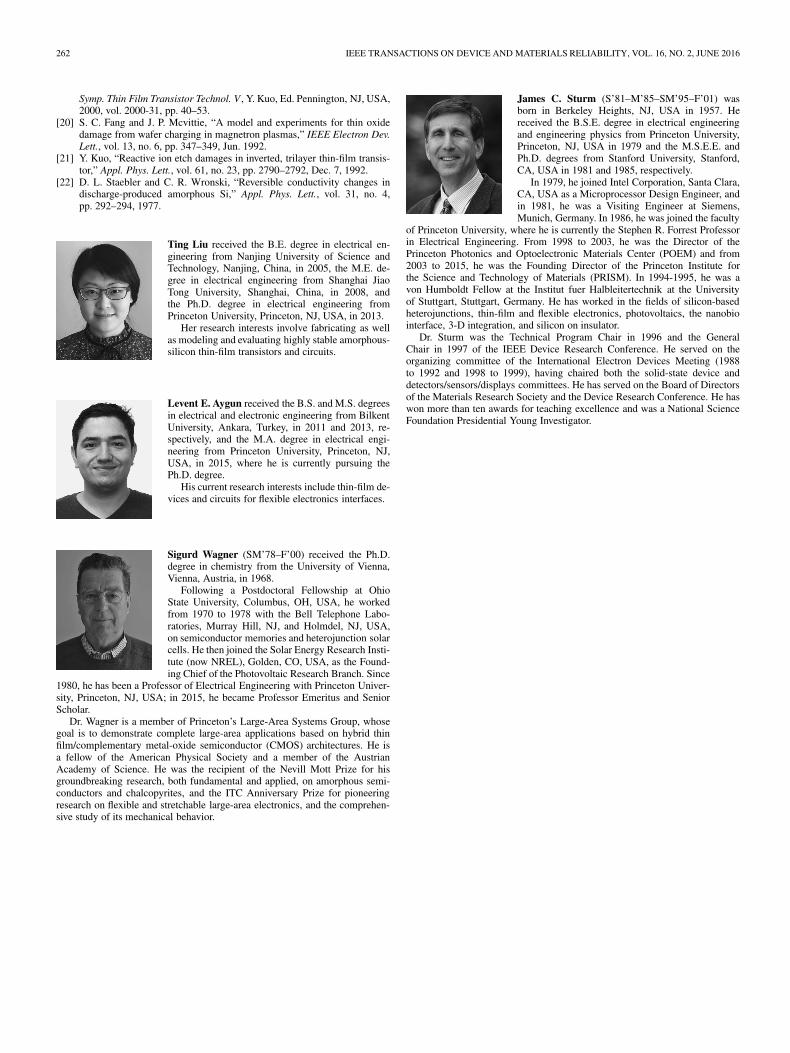
Up to this point, all data presented in this paper has beenfor a gate-source voltage of 5 V. We now briefly examine thedegradation at different gate voltages. Fig. 8 presents normal-ized drain current versus time for TFT’s fabricated similar tothose analyzed in process #5 in Table II, but two years earlierthan those devices. Thus the devices might not behave exactlythe same as those in process #5. The degradation in saturationat gate-source voltages of 5.0 V, 7.5 V, 10.0 V, and 12.5 V arepresented, all at 60 ◦C. These voltages are still fairly “low”for operation of a-Si TFTs. The drain voltage was 2.5 V largerthan the gate voltage. The gate voltage has only a small effect(on a logarithmic time scale), with the 50% degradation timefor current decreasing from 2.5 × 10⁵ s to 0.9 × 10⁵ s as thegate voltage is increased from 5 V to 12.5 V. Stage I effects(which had a ∼5% effect on the current) were saturated alreadyby 1s after the bias voltage was applied. Thus to focus onStage II, the current at 1 second was used as the initial timefor normalization.
The curves were fit with the models of (1) and (3). Forparameters, v was set to 5 × 10⁵ Hz as in Table II process #5,and T0 of 830 K was used, close to the 730 K of line 5. Ifall of the fundamental parameters of the model developed inthis paper were ideally independent of gate voltage, meaningthe model presented was exact in all physical attributes, thenormalized current versus time would be independent of gatevoltage, as gate voltage does not appear in the normalizedcurrent which results from the stretched exponential model
LIU et al.: RELIABILITY OF HIGHLY STABLE AMORPHOUS-SILICON TFTs UNDER STRESS 261
Fig. 8. Normalized current in saturation at gate voltages of 5.0, 7.5, 10.0, and12.5 V at 60 ◦C for TFT’s fabricated similarly to those of Table II, process#5. Stage II fits are also presented using β = 0.4, v = 5 × 10⁵, and effectiveactivation energy Eact,eff of 790, 788, 777, and 765 meV for the four gatevoltages, respectively. The inset shows the dependence of Eact,eff on gatevoltage.
[(29) from Part I of this paper]:
ID,nor(t) = exp
[−2
(t
t0,eff,II
)β]. (10)
At high gate voltages, a higher threshold shift is required toreduce drain current by a fractional amount compared to a low-gate-voltage condition, but at high gate voltages the higherchannel electron density leads to a faster threshold shift, afundamental assumption of our model.
Such ideality rarely occurs in practice; to use the models ofthis paper to span different gate voltages, we empirically ad-justed one parameter, the effective activation energy Eact,eff,II
(8) as a function of gate voltage. Physically, this could resultfrom the higher Fermi level at high carrier densities—a higherfraction of the electrons could then be able to physically accessthe weak bond sites to enable bond-breaking (reducing nch,o
and thusEact,eff,II ). The dependence of Eact,eff,II on gate volt-age is shown as an inset in Fig. 8, with a slope of −3.5 meV/V.This slope was fairly insensitive to the fit; changing T0 to 730 Kchanged the slope by only ∼10%. With knowledge of the slopeof Eact,eff,II versus gate voltage, one can use data for Stage IIextracted at one gate voltage to predict degradation at othergate voltages. Further work is necessary to determine if thisdependence of Eact,eff,II on gate voltage is sensitive to processconditions.
VI. SUMMARY
Using results from low gate-field stress over a range of tem-peratures and their fit to a two-stage model for threshold voltageshift, we evaluated the effect of a-Si TFT fabrication processeson the stability of the drain current in saturation with VGS =5 V. The two-stage model is necessary because the initial degra-dation at room temperature is dominated by charge trapping inthe gate SiNx, but the dominant long term mechanism is defect
creation in the a-Si. Achieving high stability requires a high(∼320 ◦C) deposition temperature for the gate SiNx and thea-Si, hydrogen dilution for the SiNx deposition, and low a-Sideposition power near the SiNx interface. By combining thesedeposition techniques, we raised the extrapolated 50% lifetimeof the drain current under continuous operation at room temper-ature in saturation with VGS = 5 V from 3.3 × 10⁴ s (9.2 hours)to 4.4 × 10⁷ s (1.4 years) for a dry-etch process. We alsoshowed how degradation at one gate voltage is related to thatat other gate voltages. Further improvement in stability may bepossible by minimizing damage from plasma-etch steps duringprocessing.
REFERENCES
[1] J. Kanicki, Amorphous and Microcrystalline Semiconductor Devices:Optoelectronic Devices. Boston, MA, USA: Artech House, 1991.
[2] M. J. Powell, “The physics of amorphous-silicon thin-film transis-tors,” IEEE Trans. Electron Devices, vol. 36, no. 12, pp. 2753–2763,Dec. 1989.
[3] A. Madan, P. G. Lecomber, and W. E. Spear, “Investigation of density oflocalized states in a-Si using field-effect technique,” J. Non-CrystallineSolids, vol. 20, pp. 239–257, 1976.
[4] B. Hekmatshoar, “Highly stable amorphous silicon thin film transistorsand integration approaches for reliable organic light emitting diode dis-plays on clear plastic,” Ph.D. dissertation, Dept. Engr., Electron, andelectr., Princeton Univ., Princeton, NJ, USA, 2010.
[5] B. Hekmatshoar et al., “Highly stable amorphous-silicon thin-filmtransistors on clear plastic,” Appl. Phys. Lett., vol. 93, Jul. 21, 2008,Art. no. 032103.
[6] B. Hekmatshoar, K. H. Cherenack, S. Wagner, and J. C. Sturm, “Amor-phous silicon thin-film transistors with DC saturation current half-life ofmore than 100 years,” in Proc. IEEE IEDM, 2008, pp. 1–4.
[7] B. Hekmatshoar, S. Wagner, and J. C. Sturm, “Tradeoff regimes of life-time in amorphous silicon thin-film transistors and a universal lifetimecomparison framework,” Appl. Phys. Lett., vol. 95, no. 14, Oct. 5, 2009,Art. no. 143504.
[8] B. Dunnett et al., “Equilibration in amorphous silicon nitride alloys,” inProc. Mater. Res. Soc. Symp., May 1995, vol. 377, pp. 349–354.
[9] I. D. French, C. J. Curling, and A. L. Goodyear, “Silicon nitride optimi-sation for A-Si:H TFTs used in projection LC-TVS,” in Proc. Mater. Res.Soc. Symp., 1994, vol. 336, pp. 769–774.
[10] I. D. French et al., “The effect of the amorphous silicon alpha-gammatransition on thin film transistor performance,” in Proc. Mater. Res. Soc.Symp., 1997, vol. 467, pp. 875–880.
[11] R. B. Wehrspohn, S. C. Deane, I. D. French, J. Hewett, and M. J. Powell,“Stability of amorphous silicon thin film transistors,” Materials ResearchSociety Symposium Proceedings, vol. 557, pp. 365–370, 1999.
[12] S. M. GadelRab, A. M. Miri, and S. G. Chamberlain, “A comparison ofthe performance and reliability of wet-etched and dry-etched alpha-Si:H TFT’s,” IEEE Trans. Electron Devices, vol. 45, no. 2, pp. 560–563,Feb. 1998.
[13] T. Liu, S. Wagner, and J. C. Sturm, “A new method for predicting thelifetime of highly stable amorphous-silicon thin-film transistors from ac-celerated tests,” in Proc. IEEE IRPS, 2011, pp. 2E.3.1–2E.3.5.
[14] A. M. Miri and S. G. Chamberlain, “A totally wet etch fabrication tech-nology for amorphous silicon thin film transistors,” in Proc. Mater. Res.Soc. Symp., 1995, vol. 377, pp. 737–742.
[15] D. Murley, I. French, S. Deane, and R. Gibson, “The effect of hydrogendilution on the aminosilane plasma regime used to deposit nitrogen-richamorphous silicon nitride,” J. Non-Crystalline Solids, vol. 198, May 1996,pp. 1058–1062.
[16] D. L. Smith, A. S. Alimonda, C. C. Chen, S. E. Ready, and B. Wacker,“Mechanism of SiNxHy Deposition from NH3-SiH4 Plasma,” J. Elec-trochem. Soc., vol. 137, pp. 614–623, Feb. 1990.
[17] K. Hiranaka, T. Yoshimura, and T. Yamaguchi, “Influence of an a-SiNx:Hgate insulator on an amorphous silicon thin-film transistor,” J. Appl. Phys.,vol. 62, pp. 2129–2135, 1987.
[18] T. Yoshimura, K. Hiranaka, T. Yamaguchi, S. Yanagisawa, and K. Asama,“Characterization of a-Si:H near a-SiNx:H/a-Si:H interface by photolumi-nescence spectra,” Mater. Res. Soc. Symp., vol. 70, pp. 373–378, 1986.
[19] I. D. French, P. R. I. Cabarroca, S. C. Deane, R. B. Wehrspohn, andJ. M. Powell, “Microcrystalline silicon TFT’s for AMLCDs,” in Proc. Int.
262 IEEE TRANSACTIONS ON DEVICE AND MATERIALS RELIABILITY, VOL. 16, NO. 2, JUNE 2016
Symp. Thin Film Transistor Technol. V , Y. Kuo, Ed. Pennington, NJ, USA,2000, vol. 2000-31, pp. 40–53.
[20] S. C. Fang and J. P. Mcvittie, “A model and experiments for thin oxidedamage from wafer charging in magnetron plasmas,” IEEE Electron Dev.Lett., vol. 13, no. 6, pp. 347–349, Jun. 1992.
[21] Y. Kuo, “Reactive ion etch damages in inverted, trilayer thin-film transis-tor,” Appl. Phys. Lett., vol. 61, no. 23, pp. 2790–2792, Dec. 7, 1992.
[22] D. L. Staebler and C. R. Wronski, “Reversible conductivity changes indischarge-produced amorphous Si,” Appl. Phys. Lett., vol. 31, no. 4,pp. 292–294, 1977.
Ting Liu received the B.E. degree in electrical en-gineering from Nanjing University of Science andTechnology, Nanjing, China, in 2005, the M.E. de-gree in electrical engineering from Shanghai JiaoTong University, Shanghai, China, in 2008, andthe Ph.D. degree in electrical engineering fromPrinceton University, Princeton, NJ, USA, in 2013.
Her research interests involve fabricating as wellas modeling and evaluating highly stable amorphous-silicon thin-film transistors and circuits.
Levent E. Aygun received the B.S. and M.S. degreesin electrical and electronic engineering from BilkentUniversity, Ankara, Turkey, in 2011 and 2013, re-spectively, and the M.A. degree in electrical engi-neering from Princeton University, Princeton, NJ,USA, in 2015, where he is currently pursuing thePh.D. degree.
His current research interests include thin-film de-vices and circuits for flexible electronics interfaces.
Sigurd Wagner (SM’78–F’00) received the Ph.D.degree in chemistry from the University of Vienna,Vienna, Austria, in 1968.
Following a Postdoctoral Fellowship at OhioState University, Columbus, OH, USA, he workedfrom 1970 to 1978 with the Bell Telephone Labo-ratories, Murray Hill, NJ, and Holmdel, NJ, USA,on semiconductor memories and heterojunction solarcells. He then joined the Solar Energy Research Insti-tute (now NREL), Golden, CO, USA, as the Found-ing Chief of the Photovoltaic Research Branch. Since
1980, he has been a Professor of Electrical Engineering with Princeton Univer-sity, Princeton, NJ, USA; in 2015, he became Professor Emeritus and SeniorScholar.
Dr. Wagner is a member of Princeton’s Large-Area Systems Group, whosegoal is to demonstrate complete large-area applications based on hybrid thinfilm/complementary metal-oxide semiconductor (CMOS) architectures. He isa fellow of the American Physical Society and a member of the AustrianAcademy of Science. He was the recipient of the Nevill Mott Prize for hisgroundbreaking research, both fundamental and applied, on amorphous semi-conductors and chalcopyrites, and the ITC Anniversary Prize for pioneeringresearch on flexible and stretchable large-area electronics, and the comprehen-sive study of its mechanical behavior.
James C. Sturm (S’81–M’85–SM’95–F’01) wasborn in Berkeley Heights, NJ, USA in 1957. Hereceived the B.S.E. degree in electrical engineeringand engineering physics from Princeton University,Princeton, NJ, USA in 1979 and the M.S.E.E. andPh.D. degrees from Stanford University, Stanford,CA, USA in 1981 and 1985, respectively.
In 1979, he joined Intel Corporation, Santa Clara,CA, USA as a Microprocessor Design Engineer, andin 1981, he was a Visiting Engineer at Siemens,Munich, Germany. In 1986, he was joined the faculty
of Princeton University, where he is currently the Stephen R. Forrest Professorin Electrical Engineering. From 1998 to 2003, he was the Director of thePrinceton Photonics and Optoelectronic Materials Center (POEM) and from2003 to 2015, he was the Founding Director of the Princeton Institute forthe Science and Technology of Materials (PRISM). In 1994-1995, he was avon Humboldt Fellow at the Institut fuer Halbleitertechnik at the Universityof Stuttgart, Stuttgart, Germany. He has worked in the fields of silicon-basedheterojunctions, thin-film and flexible electronics, photovoltaics, the nanobiointerface, 3-D integration, and silicon on insulator.
Dr. Sturm was the Technical Program Chair in 1996 and the GeneralChair in 1997 of the IEEE Device Research Conference. He served on theorganizing committee of the International Electron Devices Meeting (1988to 1992 and 1998 to 1999), having chaired both the solid-state device anddetectors/sensors/displays committees. He has served on the Board of Directorsof the Materials Research Society and the Device Research Conference. He haswon more than ten awards for teaching excellence and was a National ScienceFoundation Presidential Young Investigator.