Reliability of Electronics at Cryogenic Temperatures An ...
22
NASA Electronic Parts and Packaging Program (NEPP) Reliability of Electronics at Cryogenic Temperatures An Approach to Reliability Testing of High-Voltage Drivers at Cryogenic Temperatures Alexander Teverovsky QSS Group, Inc. Code 562, NASA GSFC, Greenbelt, MD 20771 [email protected] October 2005
Transcript of Reliability of Electronics at Cryogenic Temperatures An ...

NASA Electronic Parts and Packaging Program
(NEPP)
Reliability of Electronics at Cryogenic Temperatures
An Approach to Reliability Testing of High-Voltage Drivers at Cryogenic Temperatures
Alexander Teverovsky
QSS Group, Inc. Code 562, NASA GSFC, Greenbelt, MD 20771
October 2005
Abstract. Space exploration programs often require that sensors and instruments with related service electronics are exposed to outer space, thus subjecting them to extreme environmental conditions. In programs such as lunar and Martian expeditions and deep-space exploration these conditions include cryogenic temperatures. The major requirement for electronic components used in any space application is high reliability, which is assured by a system of screening and qualification testing and analyses designed to minimize the risk of failures during the mission. This system is well developed for components operating within the military range of temperatures (typically –55 oC to +125 oC); however, there are no established standards or guidelines that would help part engineers in developing reliability testing programs at cryogenic conditions. Moreover, the reliability of electronic devices at these conditions has not been studied sufficiently yet and information is lacking even about the performance of active and passive components at extremely low temperatures. This requires thorough analysis and planning of reliability testing for each case when a critical electronic component has to operate at cryogenic temperatures.
A micro-shutter array (MSA) in the Near-Infrared Spectrograph (NIRSPEC) instrument used in the James Webb Space Telescope (JWST) project will operate at temperatures in the range of 29 K to 32 K. A high-voltage driver (HVD) microcircuit used to control the array will be mounted on the MSA board and will also operate at these extremely low temperatures. This work analyzes reliability hazards of low-temperature conditions, evaluates the possibility of failures caused by different degradation mechanisms in microcircuits, and discusses specifics of HVD operation at cryogenic temperatures. Performance of different types of ceramic and electrolytic capacitors used for decoupling of power supply signals and/or loading of the outpus at cryogenic conditions is also discussed. Results of this work are being used to develop a reliability qualification testing plan for the HVD operating at cryogenic conditions. I. Reliability hazards at low temperatures. To assure reliable operation of microcircuits at normal conditions (~55 oC) for 10 years, a 1,000-hour life test is typically carried out at 125 oC. This life test is based on an assumption that an average activation energy of degradation mechanisms in microcircuits is Ea ~ 0.7 eV. In reality, different failure mechanisms have different Ea, varying typically from ~0.3 to ~1.2 eV [1]; however, a life test at 125 oC for 1,000 hours has a long history of application for high-reliability systems and became a standard test to assure quality of parts for space instruments.
A formal use of this approach to parts intended for operation at cryogenic conditions shows that a life test of less than 10-35 hours would be equivalent to a 10-year operation at 35 K, even for the least accelerated failure mechanisms with Ea ~ 0.3 eV. This appears advantageous, but is not really likely to be the case.
In actuality, most degradation mechanisms, which cause failures during operation of microcircuits at normal environments such as electromigration, mobile ion-induced drift, time-dependent breakdown, and corrosion will be virtually suppressed at cryogenic conditions [2]. However, there are several degradation mechanisms that are specific to low temperatures. The
2
first is the hot carrier induced degradation, which has negative activation energy and will be accelerated at cryogenic conditions [3].
Another group of failure mechanisms that gains importance at cryogenic conditions is related to mechanical stresses in silicon chips, passive components, and assemblies. Materials with different CTE are used in active elements and interconnections of microcircuits (Si, SiO2, Al, Si3N4, barrier metals, silicides, etc.). The difference in CTE causes mechanical stresses, σ ~ ∆CTE×(Tp – Top), which increase as the operational temperature, Top, decreases compared to the processing temperature, Tp, at which the stresses might be considered negligible. IBM and Intel have reported already on failures related to exposure of their microcircuits to low-temperature conditions and suggested a cold-temperature screening [4, 5].
The third group of reliability hazards, which is specific to the CMOS high-voltage drivers, is related to current and voltage spiking at the high-voltage power supply pin, VPP, and outputs of the driver. When a driver is loaded with a capacitor, C, the amplitude of the current spike is Isp = C×∆V/∆t. For high-voltage drivers, the ∆V is large by definition. At low temperatures, the rise time, ∆t, will decrease up to four times [6], thus resulting in further increasing of Isp. Due to inductance of the wires, L, the current spike would create a voltage spike Vsp = L×∆I/∆t, which might damage the part.
In this work problems of reliability testing of CMOS microcircuits at cryogenic temperatures related to hot carriers, mechanical stresses, and current spiking, as well as possible solutions for quality assurance testing, are discussed. Also, requirements and performance of decoupling capacitors and RC networks used for testing of high-voltage drivers at cryogenic conditions are considered.
Contents of this paper: I. Reliability hazards at low temperatures. II. Degradation due to hot-carrier injection. III. Degradation due to mechanical stresses.
III.1. Stress-induced voiding. III.2. Temperature cycling.
IV. Transients in high-voltage drivers. IV.1. Effect of load conditions and temperature. IV.2. Possible failure modes due to high current/voltage transients.
V. Performance of decoupling and load capacitors at cryogenic conditions. V.1. Ceramic capacitors. V.2. RC network. V.3. Tantalum and niobium capacitors.
VI. Conclusions. VII. References.
II. Degradation due to hot-carrier injection (HCI). The activation energy for HCI degradation is assumed to be between -0.1 and -0.2 eV [7]. For this case calculations show that a 10-year operation of the part at room temperature (RT) would be equivalent to only a fraction of a second at 35 K. This means that even long-term normal
3
operation of the part at room temperature will not guarantee reliable operation in cryogenic conditions.
One might try to accelerate HCI degradation by testing below operational temperatures (Top = 32 K). Considering that the accelerating factor of the testing, A(T), exponentially increases as the temperature decreases, variation of temperature during the testing, ∆T, will cause an error, δ, which also exponentially increases with temperature:
⎥⎦
⎤⎢⎣
⎡⎟⎠⎞
⎜⎝⎛
∆+−
∆−×=
∆+∆−
=TTTTk
ETTATTA a 11exp
)()(δ .
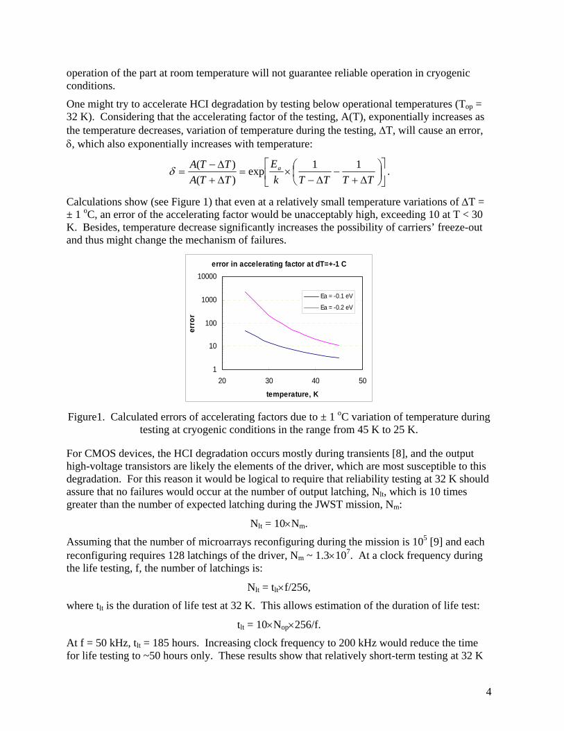
Calculations show (see Figure 1) that even at a relatively small temperature variations of ∆T = ± 1 oC, an error of the accelerating factor would be unacceptably high, exceeding 10 at T < 30 K. Besides, temperature decrease significantly increases the possibility of carriers’ freeze-out and thus might change the mechanism of failures.
error in accelerating factor at dT=+-1 C
1
10
100
1000
10000
20 30 40 50
temperature, K
erro
r
Ea = -0.1 eV
Ea = -0.2 eV
Figure1. Calculated errors of accelerating factors due to ± 1 oC variation of temperature during
testing at cryogenic conditions in the range from 45 K to 25 K.
For CMOS devices, the HCI degradation occurs mostly during transients [8], and the output high-voltage transistors are likely the elements of the driver, which are most susceptible to this degradation. For this reason it would be logical to require that reliability testing at 32 K should assure that no failures would occur at the number of output latching, Nlt, which is 10 times greater than the number of expected latching during the JWST mission, Nm:
Nlt = 10×Nm.
Assuming that the number of microarrays reconfiguring during the mission is 105 [9] and each reconfiguring requires 128 latchings of the driver, Nm ~ 1.3×10⁷. At a clock frequency during the life testing, f, the number of latchings is:
Nlt = tlt×f/256,
where tlt is the duration of life test at 32 K. This allows estimation of the duration of life test:
tlt = 10×Nop×256/f.
At f = 50 kHz, tlt = 185 hours. Increasing clock frequency to 200 kHz would reduce the time for life testing to ~50 hours only. These results show that relatively short-term testing at 32 K
4
might provide the necessary assurance that HCI degradation would not affect performance of the device during the mission period.
III. Degradation due to mechanical stresses.
III.1. Stress-induced voiding.
At low temperatures aluminum metallization embedded between SiO2/Si3N4 layers is under significant tensile stresses, which might diverge along the metallization runs due to design and structural variations. A gradient of these stresses causes flow of metal atoms and results in a void formation, increased electrical resistance, and acceleration of electromigration-induced failures.
The time to failure for this mechanism can be written as [7]:
( ) ⎟⎠⎞
⎜⎝⎛
×−×−×= −
TkE
TTAT anF exp0 ,
where: T0 is the stress-free temperature for the metal; n = 2 to 3, ( ~5 if creep, when T > Tm/2); Ea = 0.5 to 0.6 eV for grain-boundary diffusion and Ea ~1 eV for intra-grain diffusion.
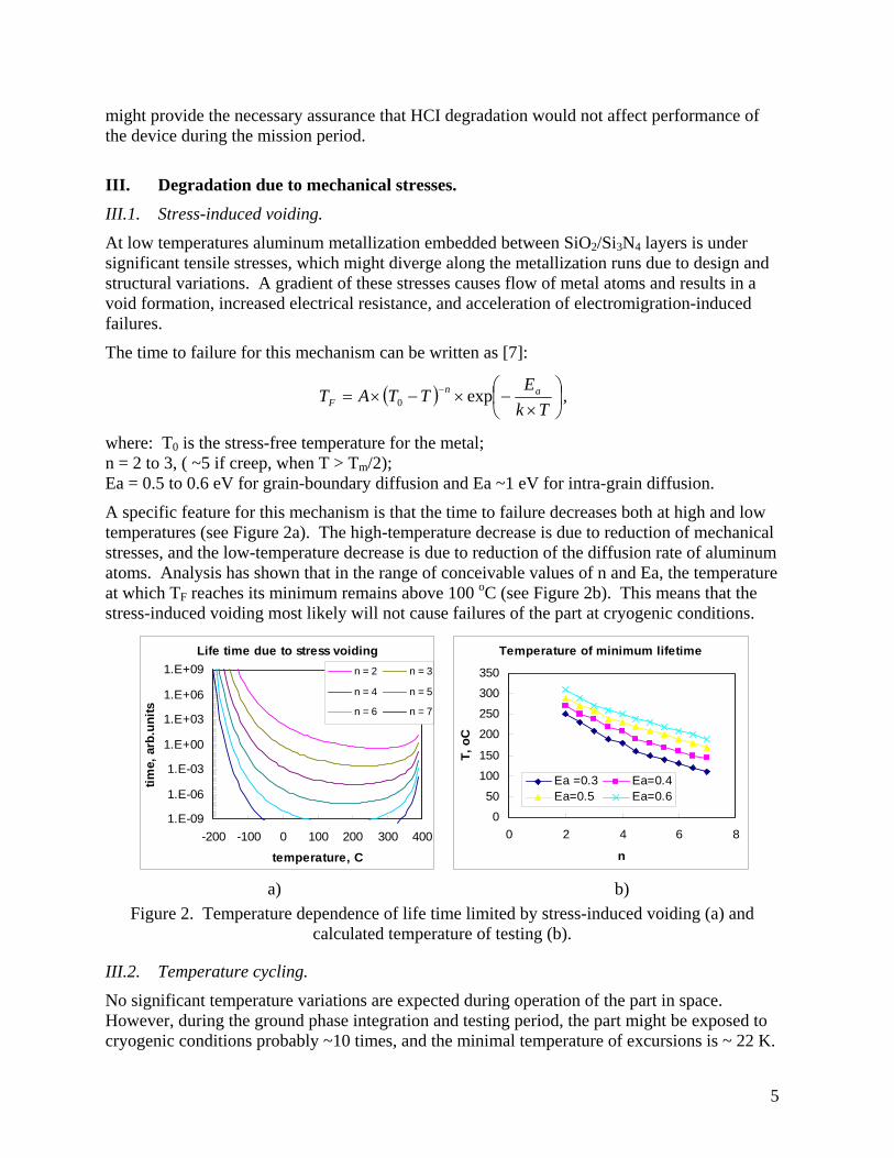
A specific feature for this mechanism is that the time to failure decreases both at high and low temperatures (see Figure 2a). The high-temperature decrease is due to reduction of mechanical stresses, and the low-temperature decrease is due to reduction of the diffusion rate of aluminum atoms. Analysis has shown that in the range of conceivable values of n and Ea, the temperature at which TF reaches its minimum remains above 100 oC (see Figure 2b). This means that the stress-induced voiding most likely will not cause failures of the part at cryogenic conditions.
Life time due to stress voiding
1.E-09
1.E-06
1.E-03
1.E+00
1.E+03
1.E+06
1.E+09
-200 -100 0 100 200 300 400
temperature, C
time,
arb
.uni
ts
n = 2 n = 3
n = 4 n = 5
n = 6 n = 7
Temperature of minimum lifetime
0
50
100
150
200
250
300
350
0 2 4 6
n
T, o
C
8
Ea =0.3 Ea=0.4Ea=0.5 Ea=0.6
a) b)
Figure 2. Temperature dependence of life time limited by stress-induced voiding (a) and calculated temperature of testing (b).
III.2. Temperature cycling.
No significant temperature variations are expected during operation of the part in space. However, during the ground phase integration and testing period, the part might be exposed to cryogenic conditions probably ~10 times, and the minimal temperature of excursions is ~ 22 K.
5
To assure that no failures will be caused by these exposures, it is reasonable to require that the parts would withstand the number of temperature cycles, which is approximately three times greater than the expected worst-case number of the exposures.
Carrying out ~30 TC between 22 K and room temperature seems to be a viable testing.
It is important to note that the rate of temperature changes for most mechanical characteristics of metals, and of Al in particular, decreases to below ~100 to 50 K. For this reason stresses at 22 K will not be much larger than at 77 K [10], and temperature cycling between room temperature (RT) and liquid nitrogen (LN) conditions, which is much easier to carry out, might provide additional easily obtained and important information regarding thermo-mechanical robustness of the devices.
The acceleration factor of failures during temperature cycling depends on the range of temperatures inducing plastic deformation, and for ductile materials, such as aluminum, can be estimated using a Coffin-Manson model [7]:
q
eo
e
TTTTA ⎟⎟
⎠
⎞⎜⎜⎝
⎛∆−∆∆−∆
= ,
where q is the Coffin-Manson exponent; ∆T is the temperature interval during accelerated testing, ∆Te is the portion of the temperature cycle range in the elastic region, and ∆To is the temperature interval during normal testing of the part.
For ductile materials ∆Te is typically negligibly small and the accelerating factor depends only on temperature swings ∆T and ∆To . For brittle materials, cracks spread rapidly with little or no plastic flow. However, fatigue failures even in normally ductile metals are the result of processes of crack nucleation and growth, which is brittle-like in nature and there is very little, if any, plastic deformation associated with failure. For this reason most likely the Coffin-Manson model in a simplified form, when ∆Te can be neglected, was successfully used even for brittle materials.
The value of the exponent q is determined empirically for different groups of materials, and for brittle materials it varies from 6 to 9. Based on these data, the number of cycles from room temperature to 77 K, which is equivalent to 30 cycles between RT and 22 K (minimum non-operational temperature), was calculated at different exponents. Results of these estimations are shown in Table 1.
Table 1. Number of RT/LN cycles equivalent to 30 TC from RT to 22 K.
q = 6 q = 7 q = 8 q = 9
115 144 181 227
Calculations indicate that positive results of ~200 temperature cycles between room temperature and liquid nitrogen conditions might prove the necessary assurance in the robustness of the parts during multiple exposures to cryogenic conditions. However, more experiments are necessary to justify applicability of Coffin-Mason model to cryogenic conditions.
6
IV. Transients in high-voltage drivers.
IV.1. Effect of load conditions and temperature.
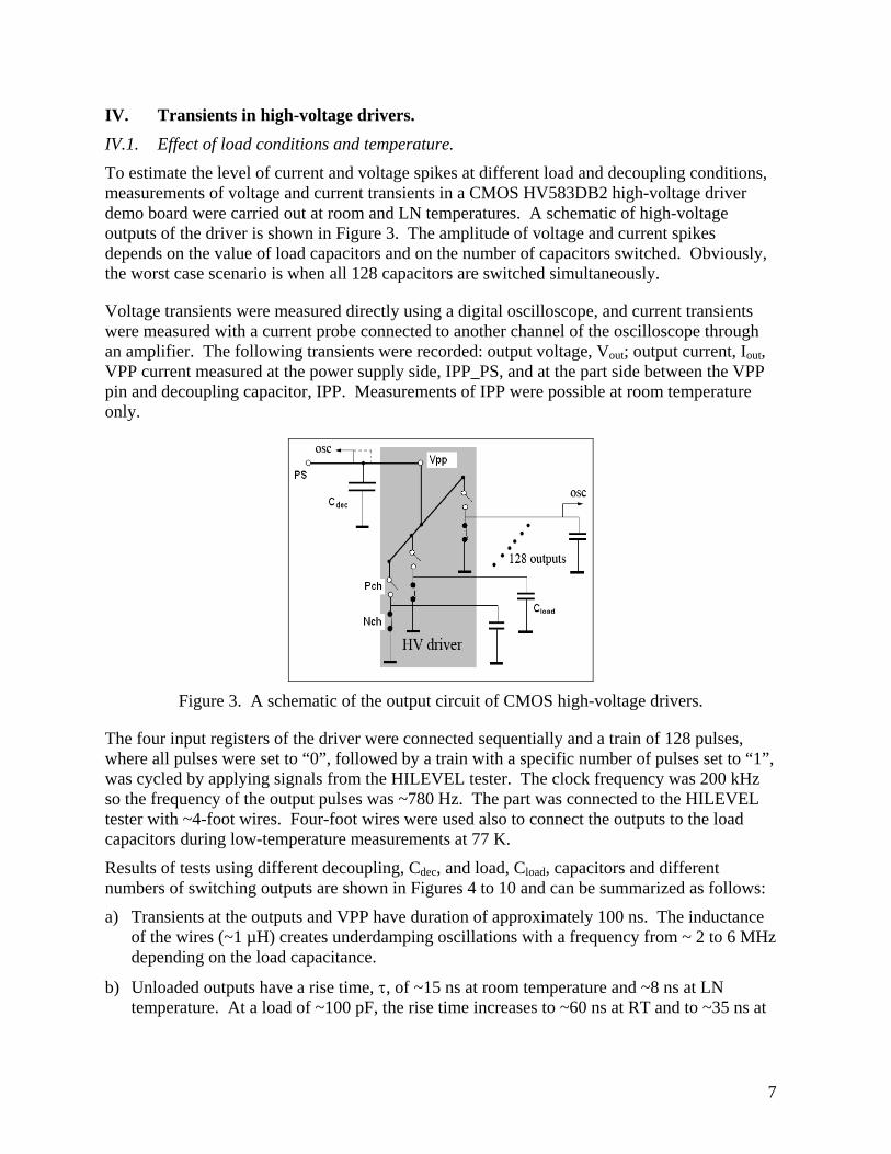
To estimate the level of current and voltage spikes at different load and decoupling conditions, measurements of voltage and current transients in a CMOS HV583DB2 high-voltage driver demo board were carried out at room and LN temperatures. A schematic of high-voltage outputs of the driver is shown in Figure 3. The amplitude of voltage and current spikes depends on the value of load capacitors and on the number of capacitors switched. Obviously, the worst case scenario is when all 128 capacitors are switched simultaneously.
Voltage transients were measured directly using a digital oscilloscope, and current transients were measured with a current probe connected to another channel of the oscilloscope through an amplifier. The following transients were recorded: output voltage, Vout; output current, Iout, VPP current measured at the power supply side, IPP_PS, and at the part side between the VPP pin and decoupling capacitor, IPP. Measurements of IPP were possible at room temperature only.
Figure 3. A schematic of the output circuit of CMOS high-voltage drivers.
The four input registers of the driver were connected sequentially and a train of 128 pulses, where all pulses were set to “0”, followed by a train with a specific number of pulses set to “1”, was cycled by applying signals from the HILEVEL tester. The clock frequency was 200 kHz so the frequency of the output pulses was ~780 Hz. The part was connected to the HILEVEL tester with ~4-foot wires. Four-foot wires were used also to connect the outputs to the load capacitors during low-temperature measurements at 77 K.
Results of tests using different decoupling, Cdec, and load, Cload, capacitors and different numbers of switching outputs are shown in Figures 4 to 10 and can be summarized as follows:
a) Transients at the outputs and VPP have duration of approximately 100 ns. The inductance of the wires (~1 µH) creates underdamping oscillations with a frequency from ~ 2 to 6 MHz depending on the load capacitance.
b) Unloaded outputs have a rise time, τ, of ~15 ns at room temperature and ~8 ns at LN temperature. At a load of ~100 pF, the rise time increases to ~60 ns at RT and to ~35 ns at
7
LN. A decrease in τ with temperature is most likely due to a decrease of the channel resistance of the output MOSFETs.
c) The amplitude of current spikes at the outputs, Iout, and at VPP, IPP increases linearly with the VPP and sublinearly with the load capacitance. At room temperature, when only one output is loaded, an increase in Cload from ~10 pF to 190 pF increases the amplitudes of spikes from 10 to 40 mA to 70 to 100 mA.
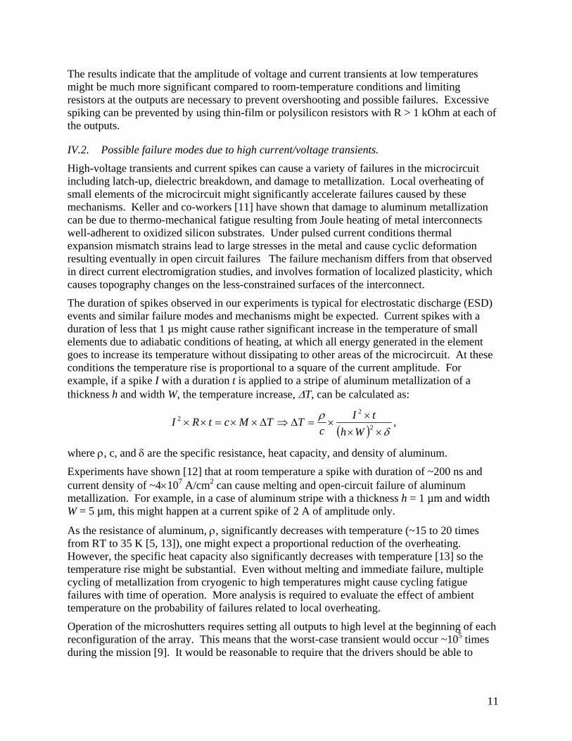
d) When six outputs are switched simultaneously at VPP = 40 V, the output overshooting, Vout_os, is below 2 V at RT and above 7 V at LN. At no-load conditions, an increase of the number of switching outputs to 128 did not cause significant overshooting at RT, but increased it to more than 25 V at LN conditions.
e) When 30 outputs were loaded with 100 pF each, the Vout_os increased to 15 V at RT and to 25 V at LN. The output current spikes at these conditions were ~0.04 A and 0.5 A at RT and LN, respectively.
f) Switching of all 128 outputs at RT and VPP = 40 V causes IPP spiking with an amplitude of ~0.24 A at no-load conditions and ~0.6 A when 30 outputs are loaded with 100 pF capacitors. Similar load conditions at cryogenic temperatures would most likely cause IPP spiking above 1 A.
g) At relatively mild load conditions, Ta capacitors at VPP reduce transients at the power supply lines significantly even at LN conditions. However, when 30 outputs were loaded with 100 pF capacitors, the power supply current spike was anomalously high, IPP_PS = 0.38 A.
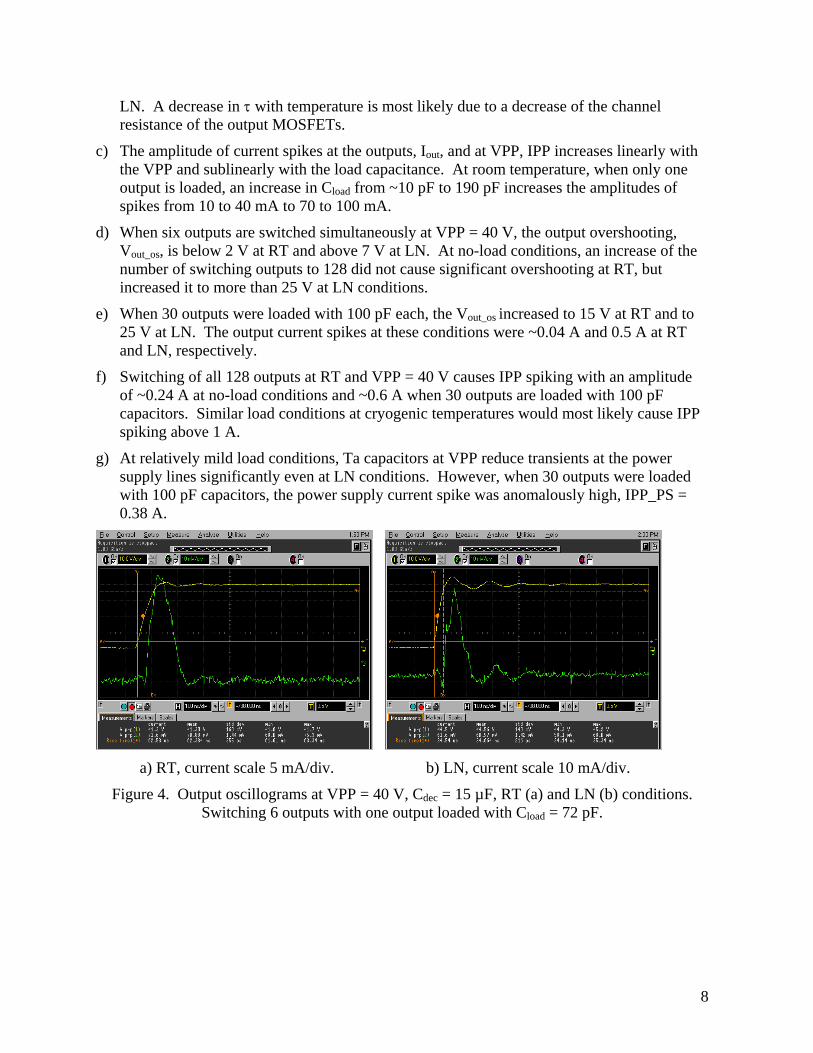
a) RT, current scale 5 mA/div. b) LN, current scale 10 mA/div.
Figure 4. Output oscillograms at VPP = 40 V, Cdec = 15 µF, RT (a) and LN (b) conditions. Switching 6 outputs with one output loaded with Cload = 72 pF.
8

VPP=40V
30
35
40
45
50
200 400 600 800 1000time, ns
Vout
, V
Vout RT no capVout RT 15 uFVout RT 0.1 uF
VPP=40V
30
35
40
45
50
200 400 600 800 1000time, ns
Vou
t, V
Vout LN no capVout LN 15 uFVout LN 0.1 uF
a) RT b) LN Figure 5. Effect of decoupling capacitors on output transients at RT (a) and LN (b) conditions. C load = 72 pF. Six
outputs were switched during these measurements and only one output was loaded with 72 pF.
RT Cvpp=4.7uF+0.1uF, Cload=72 pF
0
0.02
0.04
0.06
0.08
0.1
0.12
30 50 70 90VPP, V
curre
nt s
pike
, A
0123456789
outp
ut o
vers
hut,
V
IPP, AIout, AVout_os
RT, VPP=60 V, Cvpp=4.7uF+0.1uF
0
0.02
0.04
0.06
0.08
0.1
0.12
0 25 50 75 100
125
150
175
200C load, pF
curr
ent s
pike
, A
01
23
45
67
outp
ut o
vers
hut,
V
IPP, AIout, AVout_os
a) b)
Figure 6. Effect of VPP voltage (a) and load capacitance (b) on transients at RT. Six outputs were switched during these measurements and only one output was loaded with 72 pF.
RT, VPP=40, no output load, Cvpp=15 uF
-100
10203040506070
300 350 400 450 500time, ns
Vout
, V
Vout_1Vout_3Vout_10Vout_30Vout_128
LN, VPP=40, no output load, Cvpp=15 uF
-100
10203040506070
300 350 400 450 500time, ns
Vout
, V
Vout_1Vout_3Vout_10Vout_30Vout_128
a) b) Figure 7. Effect of the number of latching outputs (1, 3, 10, 30, 128) at no-load conditions on
the voltage output transient at RT (a) and LN (b).
9
RT, VPP=40, no output load, Cvpp=15 uF
0
0.05
0.1
0.15
0.2
0.25
0.3
100 200 300 400 500time, ns
IPP,
A
IPP_1IPP_3IPP_10IPP_30IPP_128
RT, VPP=40, no output load, Cvpp=15 uF
0
0.005
0.01
0.015
0.02
300 400 500 600time, ns
Iout
, A
Iout_1, AIout_3, AIout_10, AIout_30, AIout_128, A
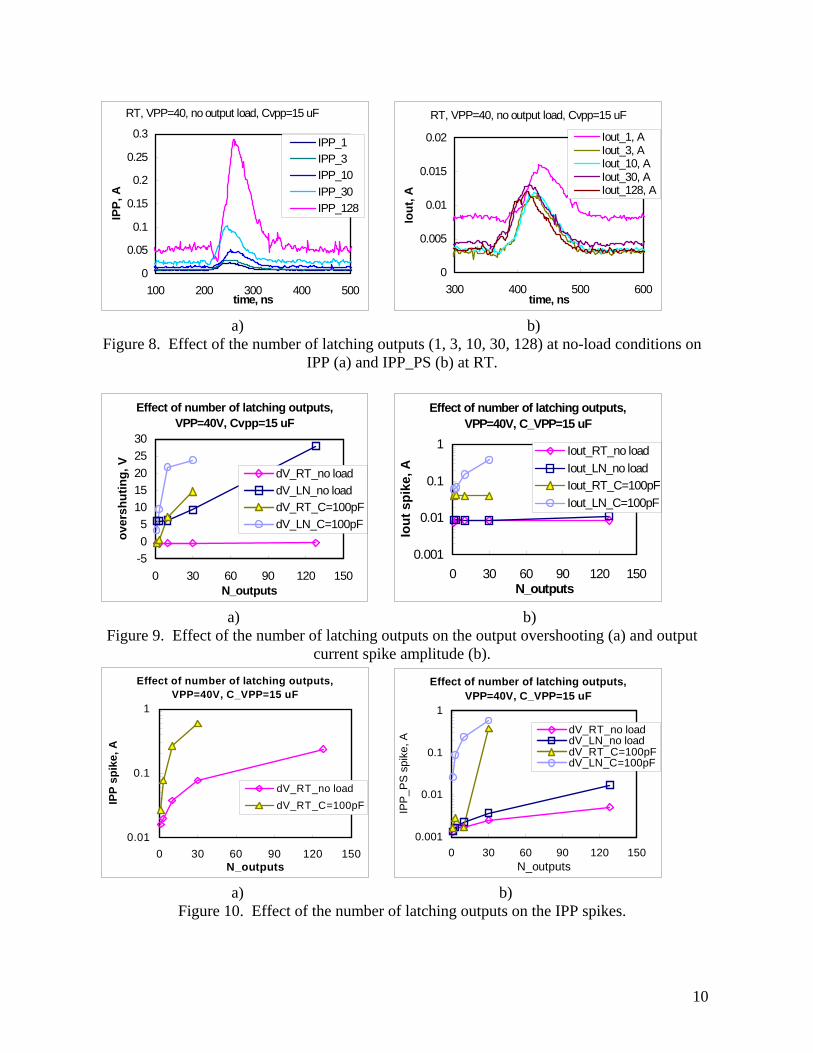
a) b) Figure 8. Effect of the number of latching outputs (1, 3, 10, 30, 128) at no-load conditions on
IPP (a) and IPP_PS (b) at RT.
Effect of number of latching outputs, VPP=40V, Cvpp=15 uF
-505
1015202530
0 30 60 90 120 150N_outputs
over
shut
ing,
V
dV_RT_no loaddV_LN_no loaddV_RT_C=100pFdV_LN_C=100pF
Effect of number of latching outputs, VPP=40V, C_VPP=15 uF
0.001
0.01
0.1
1
0 30 60 90 120 150N_outputs
Iout
spi
ke, A
Iout_RT_no loadIout_LN_no loadIout_RT_C=100pFIout_LN_C=100pF
a) b)
Figure 9. Effect of the number of latching outputs on the output overshooting (a) and output current spike amplitude (b).
Effect of number of latching outputs, VPP=40V, C_VPP=15 uF
0.01
0.1
1
0 30 60 90 120 150N_outputs
IPP
spik
e, A
dV_RT_no loaddV_RT_C=100pF
Effect of number of latching outputs, VPP=40V, C_VPP=15 uF
0.001
0.01
0.1
1
0 30 60 90 120 150N_outputs
IPP
_PS
spi
ke, A
dV_RT_no loaddV_LN_no loaddV_RT_C=100pFdV_LN_C=100pF
a) b)
Figure 10. Effect of the number of latching outputs on the IPP spikes.
10
The results indicate that the amplitude of voltage and current transients at low temperatures might be much more significant compared to room-temperature conditions and limiting resistors at the outputs are necessary to prevent overshooting and possible failures. Excessive spiking can be prevented by using thin-film or polysilicon resistors with R > 1 kOhm at each of the outputs.
IV.2. Possible failure modes due to high current/voltage transients.
High-voltage transients and current spikes can cause a variety of failures in the microcircuit including latch-up, dielectric breakdown, and damage to metallization. Local overheating of small elements of the microcircuit might significantly accelerate failures caused by these mechanisms. Keller and co-workers [11] have shown that damage to aluminum metallization can be due to thermo-mechanical fatigue resulting from Joule heating of metal interconnects well-adherent to oxidized silicon substrates. Under pulsed current conditions thermal expansion mismatch strains lead to large stresses in the metal and cause cyclic deformation resulting eventually in open circuit failures The failure mechanism differs from that observed in direct current electromigration studies, and involves formation of localized plasticity, which causes topography changes on the less-constrained surfaces of the interconnect.
The duration of spikes observed in our experiments is typical for electrostatic discharge (ESD) events and similar failure modes and mechanisms might be expected. Current spikes with a duration of less that 1 µs might cause rather significant increase in the temperature of small elements due to adiabatic conditions of heating, at which all energy generated in the element goes to increase its temperature without dissipating to other areas of the microcircuit. At these conditions the temperature rise is proportional to a square of the current amplitude. For example, if a spike I with a duration t is applied to a stripe of aluminum metallization of a thickness h and width W, the temperature increase, ∆T, can be calculated as:
( ) δρ
×××
×=∆⇒∆××=×× 2
22
WhtI
cTTMctRI ,
where ρ, c, and δ are the specific resistance, heat capacity, and density of aluminum.
Experiments have shown [12] that at room temperature a spike with duration of ~200 ns and current density of ~4×10⁷ A/cm2 can cause melting and open-circuit failure of aluminum metallization. For example, in a case of aluminum stripe with a thickness h = 1 µm and width W = 5 µm, this might happen at a current spike of 2 A of amplitude only.
As the resistance of aluminum, ρ, significantly decreases with temperature (~15 to 20 times from RT to 35 K [5, 13]), one might expect a proportional reduction of the overheating. However, the specific heat capacity also significantly decreases with temperature [13] so the temperature rise might be substantial. Even without melting and immediate failure, multiple cycling of metallization from cryogenic to high temperatures might cause cycling fatigue failures with time of operation. More analysis is required to evaluate the effect of ambient temperature on the probability of failures related to local overheating.
Operation of the microshutters requires setting all outputs to high level at the beginning of each reconfiguration of the array. This means that the worst-case transient would occur ~105 times during the mission [9]. It would be reasonable to require that the drivers should be able to
11
withstand the worst-case condition transients, when all 128 outputs are switching together, for at least 106 times at 32 K. This test should be a part of the reliability qualification testing.
V. Performance of decoupling and load capacitors at cryogenic conditions. Tantalum and/or ceramic capacitors are typically used at the power supply pins of microcircuits to short high-frequency signals and provide the necessary charge during burst increases of the load currents. The decoupling capacitors should have minimal effective series resistance (ESR) and a value that should be about nine times greater than the sum of the switched capacitors [14] so that the VPP voltage would not change significantly during discharging. In our case, assuming that each output of the HVD will be loaded with a 1 nF capacitor, the required capacitance should be above ~1 µF.
Typically, most capacitors decrease their capacitance [15] as the temperature decreases. However, the rate of temperature variations can change significantly for varying types of parts. Also, there is no sufficient information in literature regarding ESR variations with temperature. This requires measurements of characteristics of each candidate for decoupling applications at cryogenic conditions.
V.1. Ceramic capacitors.
The most popular types of ceramic capacitors are Y5V, X5R, X7R, and NPO types. All these capacitors are based on barium titanate ceramic; however, depending on dopants and composition, their temperature dependence varies significantly. Based on literature data, the thermal stability of the capacitors decreases in the row NPO, X7R, X5R, and Y5V.
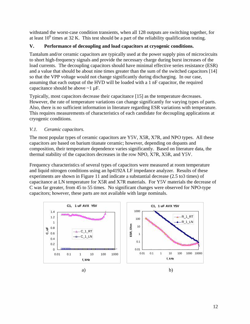
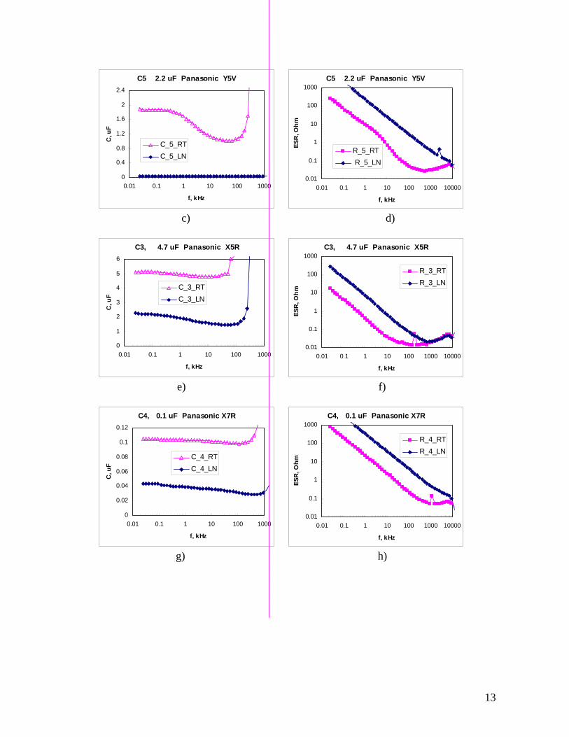
Frequency characteristics of several types of capacitors were measured at room temperature and liquid nitrogen conditions using an hp4192A LF impedance analyzer. Results of these experiments are shown in Figure 11 and indicate a substantial decrease (2.5 to3 times) of capacitance at LN temperature for X5R and X7R materials. For Y5V materials the decrease of C was far greater, from 45 to 55 times. No significant changes were observed for NPO-type capacitors; however, these parts are not available with large nominals.
C1, 1 uF AVX Y5V
0
0.2
0.4
0.6
0.8
1
1.2
1.4
0.01 0.1 1 10 100 1000
f, kHz
C, u
F
C_1_RTC_1_LN
C1, 1 uF AVX Y5V
0.01
0.1
1
10
100
1000
0.01 0.1 1 10 100 1000 10000
f, kHz
ESR
, Ohm
R_1_RTR_1_LN
a) b)
12
C5 2.2 uF Panasonic Y5V
0
0.4
0.8
1.2
1.6
2
2.4
0.01 0.1 1 10 100 1000
f, kHz
C, u
F
C_5_RTC_5_LN
C5 2.2 uF Panasonic Y5V
0.01
0.1
1
10
100
1000
0.01 0.1 1 10 100 1000 10000
f, kHz
ESR
, Ohm
R_5_RT R_5_LN
c) d)
C3, 4.7 uF Panasonic X5R
0
1
2
3
4
5
6
0.01 0.1 1 10 100 1000
f, kHz
C, u
F
C_3_RTC_3_LN
C3, 4.7 uF Panasonic X5R
0.01
0.1
1
10
100
1000
0.01 0.1 1 10 100 1000 10000
f, kHz
ESR
, Ohm
R_3_RTR_3_LN
e) f)
C4, 0.1 uF Panasonic X7R
0
0.02
0.04
0.06
0.08
0.1
0.12
0.01 0.1 1 10 100 1000
f, kHz
C, u
F
C_4_RTC_4_LN
C4, 0.1 uF Panasonic X7R
0.01
0.1
1
10
100
1000
0.01 0.1 1 10 100 1000 10000
f, kHz
ESR
, Ohm
R_4_RTR_4_LN
g) h)
13
0.1 uF KEMET X7R
0
0.02
0.04
0.06
0.08
0.1
0.12
0.01 0.1 1 10 100 1000
frequency, kHz
C, u
F
0.1 uF KEMET X7R
0.01
0.1
1
10
100
1000
0.01 0.1 1 10 100 1000 10000
frequency, kHz
ES
R, O
hm
i) j)
C6 0.01 uF AVX NPO
0.009
0.0095
0.01
0.0105
0.011
0.01 0.1 1 10 100 1000
f, kHz
C, u
F
C_111_RTC_111_LN
C6 0.01 uF AVX NPO
0.01
0.1
1
10
100
0.1 1 10 100 1000 10000
f, kHz
ESR
, Ohm
R_111_RT
R_111_LN
k) l)
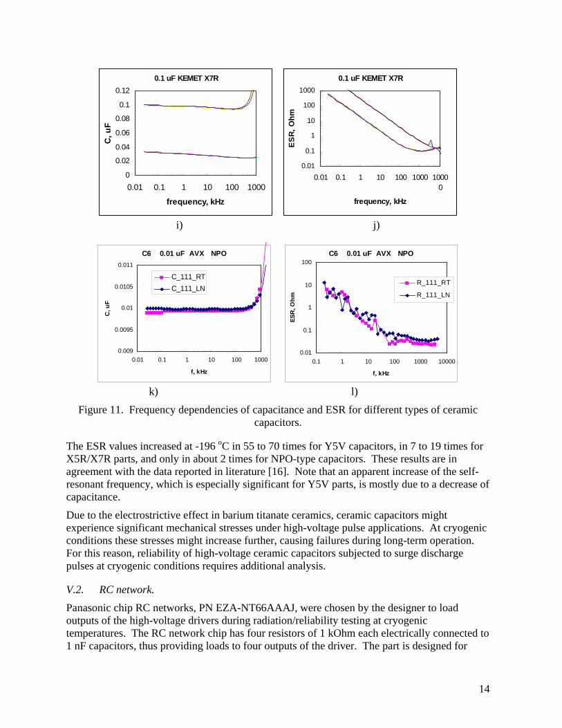
Figure 11. Frequency dependencies of capacitance and ESR for different types of ceramic capacitors.
The ESR values increased at -196 oC in 55 to 70 times for Y5V capacitors, in 7 to 19 times for X5R/X7R parts, and only in about 2 times for NPO-type capacitors. These results are in agreement with the data reported in literature [16]. Note that an apparent increase of the self-resonant frequency, which is especially significant for Y5V parts, is mostly due to a decrease of capacitance.
Due to the electrostrictive effect in barium titanate ceramics, ceramic capacitors might experience significant mechanical stresses under high-voltage pulse applications. At cryogenic conditions these stresses might increase further, causing failures during long-term operation. For this reason, reliability of high-voltage ceramic capacitors subjected to surge discharge pulses at cryogenic conditions requires additional analysis.
V.2. RC network.
Panasonic chip RC networks, PN EZA-NT66AAAJ, were chosen by the designer to load outputs of the high-voltage drivers during radiation/reliability testing at cryogenic temperatures. The RC network chip has four resistors of 1 kOhm each electrically connected to 1 nF capacitors, thus providing loads to four outputs of the driver. The part is designed for
14
commercial applications in noise-reduction circuits, is rated to 50 V, and has a relatively narrow range of operating temperatures (from -25 oC to +85 oC).
Resistors and capacitors in the network are mounted on a small alumina substrate with the outer electrodes formed along the periphery of the substrate to allow assembly on the board using a surface-mount technology process. Due to a large difference in CTE between alumina ceramic and polymer board, significant mechanical stresses will develop in solder joints at cryogenic temperatures. At these conditions, mechanical integrity of the assembly might be compromised.
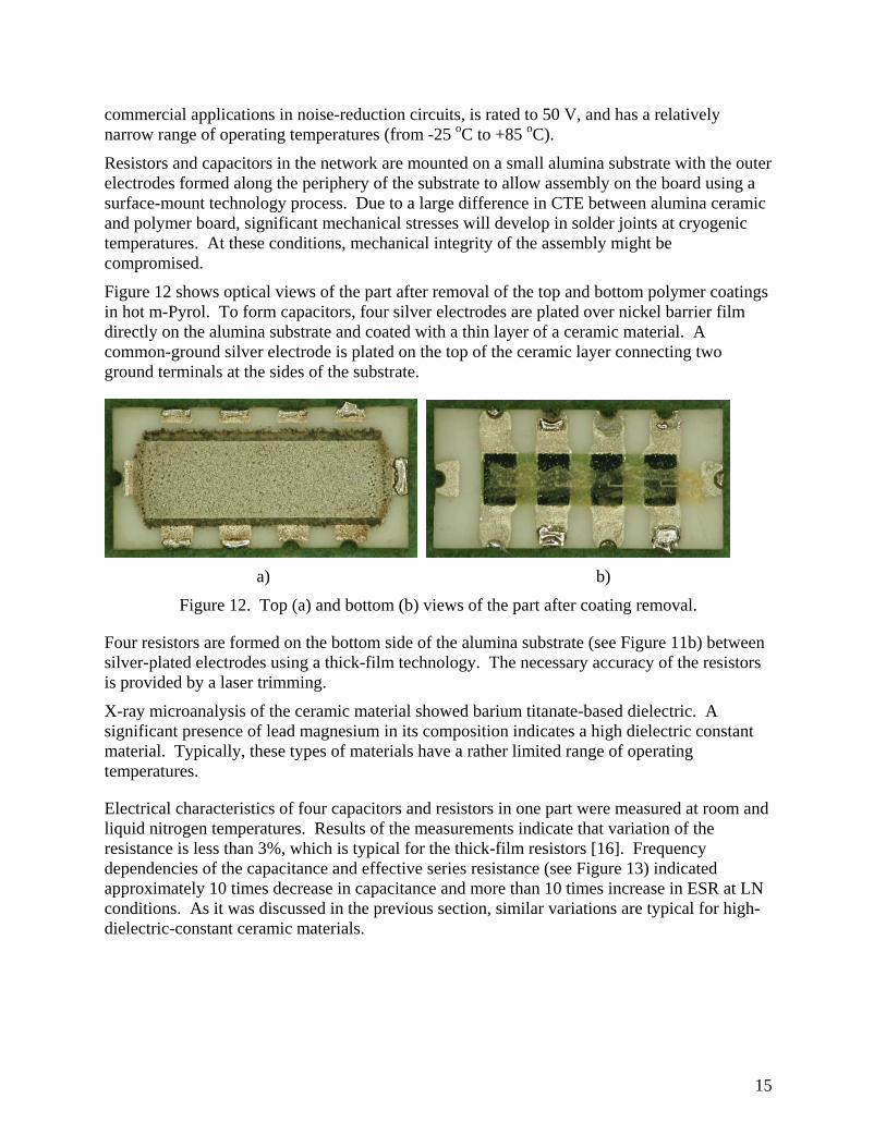
Figure 12 shows optical views of the part after removal of the top and bottom polymer coatings in hot m-Pyrol. To form capacitors, four silver electrodes are plated over nickel barrier film directly on the alumina substrate and coated with a thin layer of a ceramic material. A common-ground silver electrode is plated on the top of the ceramic layer connecting two ground terminals at the sides of the substrate.
a) b)
Figure 12. Top (a) and bottom (b) views of the part after coating removal.
Four resistors are formed on the bottom side of the alumina substrate (see Figure 11b) between silver-plated electrodes using a thick-film technology. The necessary accuracy of the resistors is provided by a laser trimming.
X-ray microanalysis of the ceramic material showed barium titanate-based dielectric. A significant presence of lead magnesium in its composition indicates a high dielectric constant material. Typically, these types of materials have a rather limited range of operating temperatures.
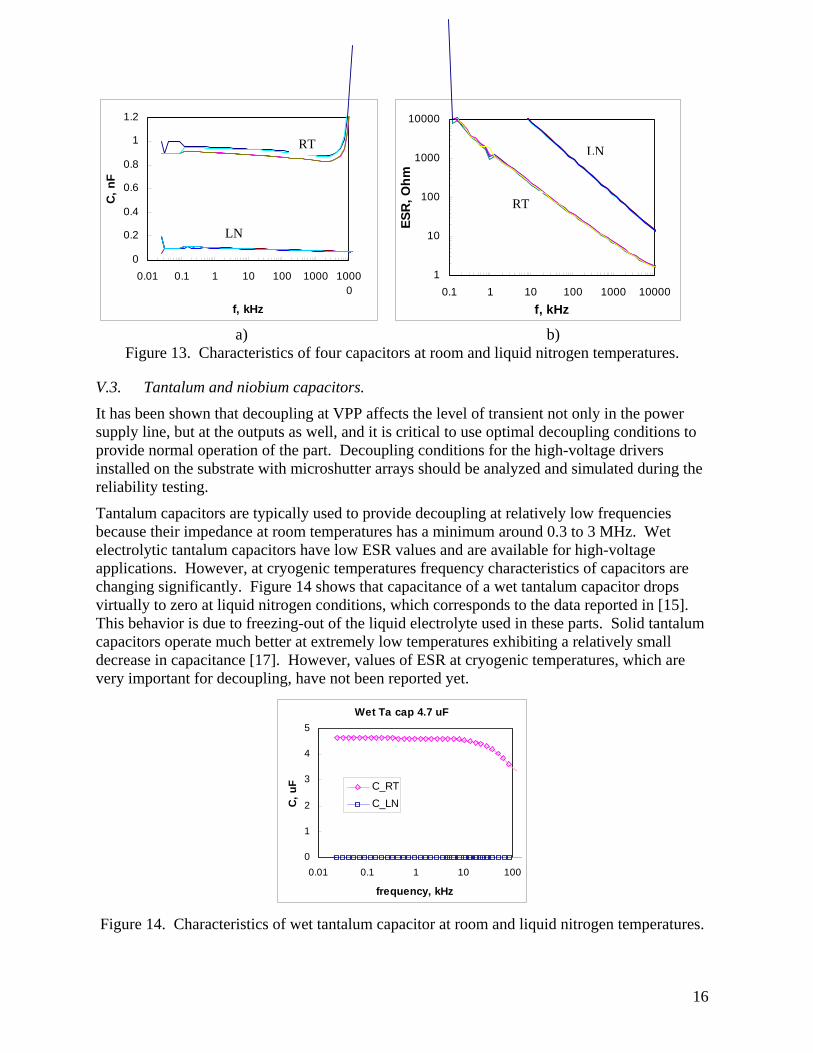
Electrical characteristics of four capacitors and resistors in one part were measured at room and liquid nitrogen temperatures. Results of the measurements indicate that variation of the resistance is less than 3%, which is typical for the thick-film resistors [16]. Frequency dependencies of the capacitance and effective series resistance (see Figure 13) indicated approximately 10 times decrease in capacitance and more than 10 times increase in ESR at LN conditions. As it was discussed in the previous section, similar variations are typical for high-dielectric-constant ceramic materials.
15
0
0.2
0.4
0.6
0.8
1
1.2
0.01 0.1 1 10 100
f, kHz
C, n
F10000
T
a) Figure 13. Characteristics
V.3. Tantalum and niobium
It has been shown that decoupsupply line, but at the outputs aprovide normal operation of thinstalled on the substrate with reliability testing.
Tantalum capacitors are typicabecause their impedance at rooelectrolytic tantalum capacitorapplications. However, at cryochanging significantly. Figurevirtually to zero at liquid nitrogThis behavior is due to freezincapacitors operate much betterdecrease in capacitance [17]. Hvery important for decoupling,
Figure 14. Characteristics of
R
10
100
1000
ESR
, Ohm
LN
LN
1000 10000
10.1 1
of four capacitors at room and liq
capacitors.
ling at VPP affects the level of tras well, and it is critical to use opte part. Decoupling conditions formicroshutter arrays should be ana
lly used to provide decoupling at m temperatures has a minimum as have low ESR values and are avgenic temperatures frequency cha 14 shows that capacitance of a wen conditions, which corresponds
g-out of the liquid electrolyte used at extremely low temperatures ex
owever, values of ESR at cryoge have not been reported yet.
Wet Ta cap 4.7 uF
0
1
2
3
4
5
0.01 0.1 1 10 1
frequency, kHz
C, u
F C_RTC_LN
wet tantalum capacitor at room an
RT
10 100
f, kHz
b) uid nitrogen
nsient not onimal decoupl the high-vollyzed and sim
relatively lowround 0.3 to ailable for hiracteristics o
et tantalum c to the data r in these parhibiting a relnic temperat
00
d liquid nitro
1000 10000
temperatures.
ly in the power ing conditions to tage drivers ulated during the
frequencies 3 MHz. Wet gh-voltage f capacitors are apacitor drops eported in [15]. ts. Solid tantalum atively small ures, which are
gen temperatures.
16

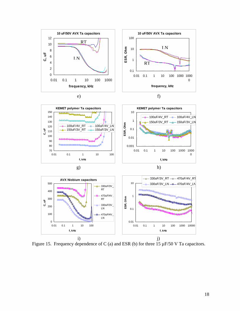
Three types of chip solid electrolytic capacitors are now available: first and currently the largest group used in military and aerospace applications is tantalum capacitors with manganese cathodes; second is relatively new tantalum capacitors with polymer cathodes; and the third is niobium capacitors, which are rapidly gaining their share in the market mostly for commercial applications. To evaluate the effect of cryogenic conditions on different types of capacitors, experiments were carried out on three 15 µF/50 V tantalum capacitors with manganese electrodes, 100 µF/4 V and 150 µF/3 V tantalum capacitors with polymer cathodes, and 330 µF/3 V and 470 µF/4 V niobium capacitors. Figure 15 shows frequency dependencies of C and ESR for these parts at room temperature and 77 K, and Table 2 shows values of capacitance measured at 1 MHz and ESR measured at 100 kHz.
15 uF/50V KEMET Ta capacitors
02468
1012141618
0.01
C, u
F
15 uF/50V KEMET Ta capacitors
1
10
100
SR, O
hm
TN
TN
10 uF
0
2
4
6
8
10
12
0.01 0
C, u
F
L
0.1 1 10 100
f, kHz
0.01
0.1
0.01 0.1 1 1
f, k
E
a) b)
/25V AVX Ta capacitors
.1 1 10 100 1000
frequency, kHz
10 uF/25V AVX Ta
0.1
1
10
100
0.01 0.1 1 10
frequen
ESR,
Ohm
T
NT
c) d)
L
RR
0 100 1000 10000
Hz
capacitors
N
L
L
RR
100 1000 10000
cy, kHz
17
10 uF/50V AVX Ta capacitors
0
2
4
6
8
10
12
0.01 0.1 1 10 100 1000
frequency, kHz
C, u
F
10 uF/50V AVX Ta capacitors
0.1
1
10
100
0.01 0.1 1 10 100 1000 10000
frequency, kHz
ESR,
Ohm
RT
e) f)
KEMET polymer Ta capacitors
70
80
90
100
110
120
130
140
150
0.01 0.1 1 10 100
f, kHz
C, u
F
100uF/4V_RT 100uF/4V_LN150uF/3V_RT 150uF/3V_LN
KEMET polymer Ta capacitors
0.001
0.01
0.1
1
10
0.01 0.1 1 10 100 1000 10000
f, kHz
ESR
, Ohm
100uF/4V_RT 100uF/4V_LN150uF/3V_RT 150uF/3V_LN
LN
LNRT
g) h)
AVX Niobium capacitors
0
100
200
300
400
500
0.01 0.1 1 10 100
f, kHz
C, u
F
330uF/3V_RT
470uF/4V_RT
330uF/3V_LN
470uF/4V_LN
0.01
0.1
1
10
0.01 0.1 1 10 100 1000 10000
f, kHz
ESR
, Ohm
330uF/3V_RT 470uF/4V_RT
330uF/3V_LN 470uF/4V_LN
i) j)
Figure 15. Frequency dependence of C (a) and ESR (b) for three 15 µF/50 V Ta capacitors.
18
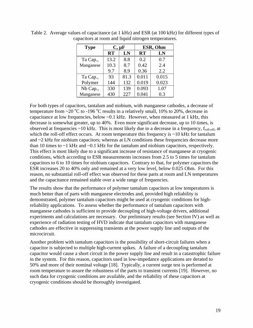
Table 2. Average values of capacitance (at 1 kHz) and ESR (at 100 kHz) for different types of capacitors at room and liquid nitrogen temperatures.
Type C, µF ESR, Ohm RT LN RT LN
Ta Cap., 13.2 8.8 0.2 0.7 Manganese 10.3 8.7 0.42 2.4
9.7 8.9 0.36 2.2 Ta Cap., 93 81.3 0.011 0.015 Polymer 144 132 0.019 0.023 Nb Cap., 330 139 0.093 1.07
Manganese 430 227 0.041 0.3
For both types of capacitors, tantalum and niobium, with manganese cathodes, a decrease of temperature from ~20 oC to -196 oC results in a relatively small, 10% to 20%, decrease in capacitance at low frequencies, below ~0.1 kHz. However, when measured at 1 kHz, this decrease is somewhat greater, up to 40%. Even more significant decrease, up to 10 times, is observed at frequencies ~10 kHz. This is most likely due to a decrease in a frequency, froll-off, at which the roll-off effect occurs. At room temperature this frequency is ~10 kHz for tantalum and ~2 kHz for niobium capacitors; whereas at LN conditions these frequencies decrease more than 10 times to ~1 kHz and ~0.1 kHz for the tantalum and niobium capacitors, respectively. This effect is most likely due to a significant increase of resistance of manganese at cryogenic conditions, which according to ESR measurements increases from 2.5 to 5 times for tantalum capacitors to 6 to 10 times for niobium capacitors. Contrary to that, for polymer capacitors the ESR increases 20 to 40% only and remained at a very low level, below 0.025 Ohm. For this reason, no substantial roll-off effect was observed for these parts at room and LN temperatures and the capacitance remained stable over a wide range of frequencies.
The results show that the performance of polymer tantalum capacitors at low temperatures is much better than of parts with manganese electrodes and, provided high reliability is demonstrated, polymer tantalum capacitors might be used at cryogenic conditions for high-reliability applications. To assess whether the performance of tantalum capacitors with manganese cathodes is sufficient to provide decoupling of high-voltage drivers, additional experiments and calculations are necessary. Our preliminary results (see Section IV) as well as experience of radiation testing of HVD indicate that tantalum capacitors with manganese cathodes are effective in suppressing transients at the power supply line and outputs of the microcircuit.
Another problem with tantalum capacitors is the possibility of short-circuit failures when a capacitor is subjected to multiple high-current spikes. A failure of a decoupling tantalum capacitor would cause a short circuit in the power supply line and result in a catastrophic failure in the system. For this reason, capacitors used in low-impedance applications are derated to 50% and more of their nominal voltage [18]. Typically, a current surge test is performed at room temperature to assure the robustness of the parts to transient currents [19]. However, no such data for cryogenic conditions are available, and the reliability of these capacitors at cryogenic conditions should be thoroughly investigated.
19
VI. Conclusions.
• Reliability hazards for HVD microcircuits operating at cryogenic temperatures have been analyzed and three types of degradation mechanisms specific to low temperatures have been revealed: parametric instability due to hot carrier injection, mechanical damage due to increased stresses during excursions to cryogenic conditions, and damage due to high-voltage and high-current transient spikes.
• The amplitude of transient spikes during switching of high-voltage outputs is significantly, more than three times, increasing at low temperatures compared to room temperature conditions. For this reason the output currents of the microcircuit should be limited with resistors of ~1 kOhm minimum.
• Both failure mechanisms, related to hot-carrier degradation and to high-voltage/high-current transients, depend on the number of latching cycles rather than on the duration of part operation at cryogenic temperatures. For this reason, instead of accelerating possible degradation by increasing of the level of stresses (e.g., lowering the temperature, increasing voltage and/or load, etc.), the possibility of which is very limited at cryogenic conditions, reliability qualification testing should be based on increased number of latching cycles.
• Qualification testing of HVD microcircuits at cryogenic temperature should simulate the worst-case electrical conditions of real applications, and the minimum number of cycles should be 10 times greater than the required number of the cycles for micro-shutters, Nop, during the mission period. At Nop = 105 this testing would require much less than 1,000 hours, which is typical for standard high-temperature life testing.
• Performance of several types of ceramic (NPO, X5R, X7R, and Y5V) and electrolytic (wet tantalum, solid tantalum, niobium, and tantalum polymer) capacitors at cryogenic conditions has been evaluated. Measurements at liquid nitrogen temperature (-196 oC) showed that the most stable are NPO-type capacitors; however, these devices are not available in large values required for HVD decoupling. The decrease of capacitance for X5R/X7R capacitors was 2.5 to 3 times; whereas for Y5V materials it was from 45 to 55 times, thus making them unusable at cryogenic conditions.
• Capacitance of wet tantalum capacitors also decreased dramatically and these parts cannot be used at cryogenic conditions due to freeze-out of the electrolyte. Solid tantalum capacitors decrease their value 30% to 40% only and they are capable of restraining transients in the VPP power supply line. The best performers were tantalum polymer capacitors with capacitance at -196 oC decreased 10% to 15% only. Most importantly, their ESR values remained stable, whereas for capacitors with manganese electrodes ESR increased 2.5 to 10 times.
• Reliable operation of decoupling capacitors is critical to avoid short-circuit failures in the system and their capability to withstand multiple high-current spikes at cryogenic conditions should be investigated additionally.
VII. References. [1]. "Failure mechanisms and models for silicon semiconductor devices", EIA/JEDEC
publication, 1996. EIA/JEP122.
20
[2]. W.F. Clark, B. El-Kareh, R.G. Pires, S.L. Titcomb, and R.L. Anderson, "Low temperature CMOS-a brief review", IEEE Transactions on Components, Hybrids, and Manufacturing Technology, 1992. 15(3), pp. 397-404.
[3]. M. Song, K. Macwilliams, and C. Woo, "Comparison of NMOS and PMOS hot carrier effects from 300 to 77 K", IEEE Transactions on Electron Devices, 1997. 44(2), pp. 268-276.
[4]. C.-W. Tseng, E.J. Mccluskey, S. Xiaoping, and D.M. Wu, "Cold delay defect screening", in Proceedings of the Proceedings of the 18th IEEE VLSI Test Symposium, 2000,30 April-4 May 2000, pp. 183-188.
[5]. M.J. Ellsworth, "The Challenge of Operating Computers at Ultra-low Temperatures", Electronics cooling, 2001, http://www.electronics-cooling.com/html/2001_august_a3.html
[6]. J. Laramee, M.J. Aubin, and J.D. Cheeke, "Behavior of CMOS inverters at cryogenic temperatures", Solid-State Electronics, 1985. 28(5), pp. 453-456.
[7]. Sematech, "Semiconductor Device Reliability Failure Models", International SEMATECH Technology Transfer, 2000(00053955A-XFR). http://www.sematech.org
[8]. V. Redy, "An introduction to CMOS semiconductor reliability", in Proceedings of the IRPS 2004, 2004, pp. 101.1-50.
[9]. R.A. S.H. Moseley, R. A. Boucarut, M. Jhabvala, T. King, G. Kletetschka, A. S. Kutyrev, M. Li, S. Meyer, D. Rapchun , and R. F. Silverberg, "Microshutters Arrays for the JWST Near Infrared Spectrograph", in Proceedings of the SPIE conference "Astronomical Telescopes and Instrumentation 2004: Space Telescopes and Astronomy", 2004, June 2004, Glasgow, Scotland, pp. 645-652. http://bram.gsfc.nasa.gov/ms_webpage/presentation/ms_pubs.html
[10]. J.G. Weisend, "Properties of Materials at Low Temperatures", in Proceedings of the JPL Workshop on Electronics For Extreme Environments, 2003,May 14-16 2003, Pasadena, CA
[11]. R.R. Keller, R.H. Geiss, Y.W. Cheng, and D.T. Read, "Electric Current Induced Thermomechanical Fatigue Testing of Interconnects", in Proceedings of the Characterization and Metrology for ULSI Technology 2005, 2005, pp. in press. http://www.boulder.nist.gov/div853/Publication%20files/NIST_MRS_Spring_2005_B9.5_Keller.pdf
[12]. K. Banerjee, A. Amerasekera, N. Cheung, and C. Hu, "High-current failure model for VLSI interconnects under short-pulse stress conditions", Electron Device Letters, 1997. 18(9), pp. 405-407.
[13]. T.M. Flynn, Cryogenic engineering. second ed. 2005: Marcel Dekker, NY. 895. [14]. A.G. Martin and R.K. Keenan, "Improved noise suppression via multilayer ceramic
capacitors (MLCs) in power-entry decoupling", AVX technical information. http://www.avxcorp.com/docs/techinfo/supvmlc.pdf
[15]. R.L. Patterson, A. Hammoud, J.E. Dickman, S. Gerber, M.E. Elbuluk, and E. Overton, "Electrical devices and circuits for low temperature space applications", in Proceedings of the International Workshop on thermal detectors (TDW03), 2003,June 19 - 20, 2003, Washington, DC. http://www-lep.gsfc.nasa.gov/code693/tdw03/proceedings/docs/session_4/Patterson.pdf
21
[16]. J. Gornto, T. Green, W. Symon, and R.W.Johnson, "Passive components for lunar and martian exploration", in Proceedings of the Reliability of advanced electronic packages and devices in extreme cold environments, 2005,February 21-23, 2005, Pasadena, CA
[17]. A. Hammoud, S. Gerber, R.L. Patterson, and T.L. Macdonald, "Performance of surface-mount ceramic and solid tantalum capacitors for cryogenic applications", in Proceedings of the Conference on Electrical Insulation and Dielectric Phenomena, Annual Report., 1998,Oct. 25-28, pp. 572-576.
[18]. J. Gill, "Surge in solid tantalum capacitors", AVX technical information, 1994. http://www.avxcorp.com/docs/techinfo/surgtant.pdf
[19]. J. Marshall and J. Primak, "Surge step stress testing of tantalum capacitors", in Proceedings of the 21st Capacitors and Resistors Technology Symposium, CARTS'01, 2001, pp. 181-187.
22