Relationship Between Signal Integrity and EMC - IEEE · Relationship Between Signal Integrity and...
32
Relationship Between Relationship Between Signal Integrity and EMC Signal Integrity and EMC Presented by Presented by Hasnain Syed Hasnain Syed Solectron USA, Inc. Solectron USA, Inc. RTP, North Carolina RTP, North Carolina Email: [email protected] Email: [email protected] 06/05/2007 Hasnain Syed 1
Transcript of Relationship Between Signal Integrity and EMC - IEEE · Relationship Between Signal Integrity and...

Relationship Between Relationship Between Signal Integrity and EMCSignal Integrity and EMC
Presented byPresented by
Hasnain SyedHasnain Syed
Solectron USA, Inc.Solectron USA, Inc.RTP, North CarolinaRTP, North Carolina
Email: [email protected]: [email protected]
06/05/2007 Hasnain Syed 1

What is Signal Integrity (SI)?What is Signal Integrity (SI)?
Signal Integrity ensures that:Signal Integrity ensures that:
Signal quality is maintained from a driver to a receiverSignal quality is maintained from a driver to a receiverInterference between two or more signals doesn’t Interference between two or more signals doesn’t degrade the signaldegrade the signalThe signals don’t damage any devicesThe signals don’t damage any devicesPower distribution network (PDN) integrity is maintainedPower distribution network (PDN) integrity is maintainedTiming margins are achievedTiming margins are achieved
06/05/2007 Hasnain Syed 2

Differences between SI and EMI (Emissions)Differences between SI and EMI (Emissions)
06/05/2007 Hasnain Syed 3
EMIEMI SISIFrequency domainFrequency domain Time domainTime domain
Voltage/current spectrum for Voltage/current spectrum for conducted emissions. Current conducted emissions. Current spectrum and radiated field spectrum spectrum and radiated field spectrum for radiated emissionsfor radiated emissions
Voltage waveformVoltage waveform
More attention is given to the clock More attention is given to the clock and I/O signalsand I/O signals
All highAll high--speed signals are analyzedspeed signals are analyzed
Common mode noise is of prime interestCommon mode noise is of prime interest Common mode noise is not that importantCommon mode noise is not that important
Noise levels of concern are in Noise levels of concern are in μμA and A and μμVV Noise levels of concern are in mA and mVNoise levels of concern are in mA and mV
Simulation is not popular. Design is based Simulation is not popular. Design is based on rule of thumbs, empirical formulason rule of thumbs, empirical formulas
Analysis based on simulations is quite Analysis based on simulations is quite commoncommon

Differences between SI and EMI (Emissions)Differences between SI and EMI (Emissions)
06/05/2007 Hasnain Syed 4
EMIEMI SISIFilters are used on clocks and I/OsFilters are used on clocks and I/Os Can have negative impact on SI Can have negative impact on SI
performanceperformance
Clock/highClock/high--speed circuitry placement speed circuitry placement with respect to the I/O circuitrywith respect to the I/O circuitry
May not be as importantMay not be as important
Clock traces are routed away from the Clock traces are routed away from the edge of the boardedge of the board
No such requirementNo such requirement
I/O connectors should not be placed on the I/O connectors should not be placed on the opposite sides of the boardopposite sides of the board
No such requirementNo such requirement
Ground flooding on signal layersGround flooding on signal layers No such requirementNo such requirement
No clock/highNo clock/high--speed traces between the speed traces between the I/O connector and the I/O circuitryI/O connector and the I/O circuitry
No such requirementNo such requirement

Differences between SI and EMI (Emissions)Differences between SI and EMI (Emissions)
06/05/2007 Hasnain Syed 5
EMIEMI SISINo clock traces on the surface layersNo clock traces on the surface layers No such requirementNo such requirement
Ground via fence around the edge of Ground via fence around the edge of the boardthe board
No such requirementNo such requirement
Decoupling caps need to be spread on Decoupling caps need to be spread on the boardthe board
No such requirementNo such requirement
Heatsink groundingHeatsink grounding No such requirementNo such requirement
PCB mounting holes to groundPCB mounting holes to ground No such requirementNo such requirement
Avoid having clocks with overlapping clock Avoid having clocks with overlapping clock harmonics. Use of spread spectrum clocks.harmonics. Use of spread spectrum clocks.
No such requirementNo such requirement

Why is Signal Integrity (SI) Needed?Why is Signal Integrity (SI) Needed?
Technology DriversTechnology DriversLower driver voltagesLower driver voltagesIncreased circuit densityIncreased circuit densityFaster edge ratesFaster edge ratesHigher data rates and clock frequenciesHigher data rates and clock frequenciesLonger signal pathsLonger signal paths
Benefits of SIBenefits of SIShorter and more predictable design cycle timeShorter and more predictable design cycle timeReduced time for prototype testing and redesignReduced time for prototype testing and redesignReduced EMIReduced EMIShorter time to marketShorter time to market
06/05/2007 Hasnain Syed 6
Interconnects affect signal quality!
As a general rule of thumb, SI analysis is required for signals with rise/fall time of less than 1 ns or with frequency 100 MHz or higher.

06/05/2007 Hasnain Syed 7
Electronic System DesignElectronic System Design
Modification Costs
Market
Pass Compliance
Schematic Board LayoutConcept System Layout Testing / Certification

Signal QualitySignal Quality
Examples of Impedance Discontinuities:Examples of Impedance Discontinuities:A change in the traceA change in the trace--widthwidthChanging reference planesChanging reference planesA gap in the reference planeA gap in the reference planeConnectorsConnectorsA branch, tee or stubA branch, tee or stubViasViasComponents connected on a traceComponents connected on a trace
06/05/2007 Hasnain Syed 8
Signal quality is affected by any impedance discontinuity that eSignal quality is affected by any impedance discontinuity that exists in the xists in the interconnect between the driver and the receiver.interconnect between the driver and the receiver.
Interconnect
Driver Receiver

Signal QualitySignal Quality
Examples of Losses introduced in the interconnects:Examples of Losses introduced in the interconnects:Skin effect lossSkin effect lossDielectric lossDielectric loss
06/05/2007 Hasnain Syed 9
Signal quality is affected by any losses that exist in the interSignal quality is affected by any losses that exist in the interconnect between connect between the driver and the receiver.the driver and the receiver.
Interconnect
Driver Receiver

Lumped vs DistributedLumped vs Distributed
06/05/2007 Hasnain Syed 10
Interconnect
Driver Receiver
L = T x vL = Length of the rising edge (inches)T = 10-90% rise time, psV = Velocity, in/ps
Interconnect size < L / 6 LumpedInterconnect size > L / 6 Distributed (transmission line)

Need for Simulations in SI AnalysisNeed for Simulations in SI AnalysisReduces the risk of failureReduces the risk of failureEnables the SI engineer to evaluate whatEnables the SI engineer to evaluate what--if scenarios early on in the if scenarios early on in the design cycledesign cycleProvides information to justify design changes and verify Provides information to justify design changes and verify effectivenesseffectivenessReduces time to marketReduces time to market
06/05/2007 Hasnain Syed 11

Device Modeling Device Modeling -- IBISIBISIBIS IBIS –– I/O Buffer Information SpecificationI/O Buffer Information SpecificationA vendorA vendor--independent format for driver/receiver modelingindependent format for driver/receiver modelingLike a black box model of a device. Internal working of the deviLike a black box model of a device. Internal working of the device ce circuitry is hidden. Useful for SPICEcircuitry is hidden. Useful for SPICE--like simulators.like simulators.Has VHas V--I and VI and V--t curves. Package parasitics can be included.t curves. Package parasitics can be included.Simulation time is smaller as compared with the transistor basedSimulation time is smaller as compared with the transistor basedSPICE models.SPICE models.
06/05/2007 Hasnain Syed 12

Termination SchemesTermination Schemes
Some examples of most commonly used termination schemes:Some examples of most commonly used termination schemes:
06/05/2007 Hasnain Syed 13
Impedance discontinuities lead to reflections. Different terminaImpedance discontinuities lead to reflections. Different termination schemes are tion schemes are employed to reduce longemployed to reduce long--line reflections and shortline reflections and short--line ringing.line ringing.
Series Termination End Termination

06/05/2007 Hasnain Syed 14
Reflection Simulation
Solution Space Analysis
Component speed, trace impedance, terminator value,trace length

EMI ImpactEMI ImpactSI analysis focuses on a voltage waveform.SI analysis focuses on a voltage waveform.From an EMI perspective the current waveform is more critical.From an EMI perspective the current waveform is more critical.Some of the intentional current flowing over the interconnects gSome of the intentional current flowing over the interconnects gets ets converted into a common mode current on a PCB.converted into a common mode current on a PCB.A reduction in the intentional current also leads to a reductionA reduction in the intentional current also leads to a reduction in the in the common mode current.common mode current.A termination scheme can be selected which can minimize the leveA termination scheme can be selected which can minimize the level l of intentional current over an interconnect while at the same tiof intentional current over an interconnect while at the same time me providing an acceptable voltage waveform at the receiver.providing an acceptable voltage waveform at the receiver.For example, a series termination is better than an end terminatFor example, a series termination is better than an end termination. ion. Also, the series termination resistor value can be optimized forAlso, the series termination resistor value can be optimized for lower lower intentional current and acceptable voltage waveform.intentional current and acceptable voltage waveform.
06/05/2007 Hasnain Syed 15

06/05/2007 Hasnain Syed 16
Voltage waveform
Current waveform

06/05/2007 Hasnain Syed 17
Problem area on the board(Near-field magnetic field scan)
Problem nets on the board(Level of noise current)
Radiation from Noise CurrentsRadiation from Noise Currents
Beforefixingthe problem

06/05/2007 Hasnain Syed 18
Problem area on the board(Near-field magnetic field scan)
Problem nets on the board(Level of noise current)
Afterfixingthe problem(addedterminationresistors onproblem nets)
Radiation from Noise CurrentsRadiation from Noise Currents

06/05/2007 Hasnain Syed 19
Changing Reference PlanesChanging Reference Planes
Vcc
GND
Impacts both SI and EMI

06/05/2007 Hasnain Syed 20
A Gap in the Reference PlaneA Gap in the Reference Plane
Return current
Signalcurrent
ReceiverDriver
Impacts both SI and EMI
Slots in the reference plane add inductance to the traces.

06/05/2007 Hasnain Syed 21
Eye Diagrams
Reflection Simulation
Solution Space AnalysisComponent speed, trace impedance, terminator value, trace length
1. Differential Signaling improves noise immunity.
2. Solves the ground bounce problem.
3. Need to reduce skew within the differential pair. Any skew within the differential pair leads to common mode noise.

06/05/2007 Hasnain Syed 22
Crosstalk SimulationCrosstalk Simulation
Solution Space AnalysisTrace width and separation
Impacts both SI and EMI

06/05/2007 Hasnain Syed 23
A Gap in the Reference PlaneA Gap in the Reference Plane
Return current
Signalcurrent
ReceiverDriver
Impacts both SI and EMI
Increased crosstalk due to shared current return path. Overlapping current loopsresult in mutual inductance causing crosstalk.

06/05/2007 Hasnain Syed 24
Crosstalk in ConnectorsCrosstalk in Connectors
Return current
Signalcurrent
ReceiverDriver
Impacts both SI and EMI
Increased crosstalk due to shared current return path. Overlapping current loopsresult in mutual inductance causing crosstalk.

06/05/2007 Hasnain Syed 25
Power Integrity SimulationPower Integrity Simulation
Impacts both SI and EMI
Minimize PCB power distribution noiseMinimize PCB power distribution noiseFulfill charge requirements of highFulfill charge requirements of high--speed devices during switchingspeed devices during switchingLow target impedance for power/ground over the frequency range oLow target impedance for power/ground over the frequency range of f interestinterest

06/05/2007 Hasnain Syed 26
Power Integrity SimulationPower Integrity Simulation
Selection of bulk and highSelection of bulk and high--frequency decoupling capacitorsfrequency decoupling capacitorsPrePre--layout analysislayout analysisPCB resonances and placement of decoupling capacitorsPCB resonances and placement of decoupling capacitorsPostPost--layout analysislayout analysisBig “V” approach (used in EMI community) vs Capacitor Array Big “V” approach (used in EMI community) vs Capacitor Array approach (more popular in the SI community)approach (more popular in the SI community)

06/05/2007 Hasnain Syed 27
Backplane SI DesignBackplane SI DesignSS--parameter analysis to determine “Insertion Loss” and “Return Losparameter analysis to determine “Insertion Loss” and “Return Loss”s”Skin effect loss, dielectric lossSkin effect loss, dielectric lossDiscontinuities like vias, connectorsDiscontinuities like vias, connectorsChannel Analysis Channel Analysis -- Tx chip to Rx chip link simulation to verify Tx chip to Rx chip link simulation to verify architecture, determine constraints and optimize designarchitecture, determine constraints and optimize designPrePre-- and postand post--layout simulationlayout simulationBackplanes can be characterized up to several GHzBackplanes can be characterized up to several GHz

06/05/2007 Hasnain Syed 28
A Typical PCB SI/EMI Design ProcessA Typical PCB SI/EMI Design Process
Schematic and BOM review Schematic and BOM review PCB stackup and layer assignmentPCB stackup and layer assignmentPrePre--route topology extraction and designroute topology extraction and designSolution Space AnalysisSolution Space Analysis–– Statistical design Statistical design -- component, manufacturing and design variances component, manufacturing and design variances
simulated. Design margins applied. Final topology template and dsimulated. Design margins applied. Final topology template and design esign constraints extracted.constraints extracted.
Constraint driven placementConstraint driven placementConstraint driven routingConstraint driven routingCritical net routing review Critical net routing review –– return current path reviewreturn current path reviewPostPost--route analysis and verificationroute analysis and verificationAn EMI rule checker can be used at various review stagesAn EMI rule checker can be used at various review stages
06/05/2007 Hasnain Syed 29
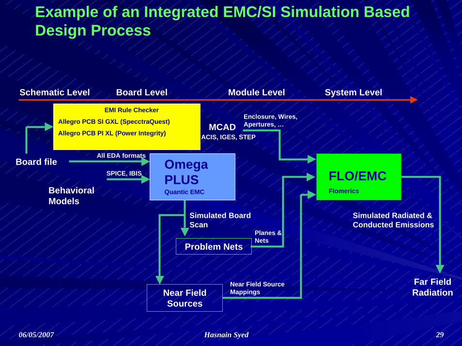
Example of an Integrated EMC/SI Simulation Based Design Process
FLO/EMCOmega PLUS
All EDA formats
ACIS, IGES, STEP
Behavioral Models
Problem NetsPlanes & Nets
MCAD
Board fileSPICE, IBIS
Simulated Board Scan
Far Field Radiation
Simulated Radiated & Conducted Emissions
Near Field Sources
Near Field Source Mappings
Quantic EMC Flomerics
Enclosure, Wires, Apertures, …
Board Level System LevelSchematic Level Module Level
EMI Rule Checker
Allegro PCB SI GXL (SpecctraQuest)
Allegro PCB PI XL (Power Integrity)

06/05/2007 Hasnain Syed 30
SI and EMI MeasurementsSI and EMI Measurements
EMI Emissions MeasurementsEMI Emissions Measurements
Are done in frequency domain using an EMI receiver or a spectrumAre done in frequency domain using an EMI receiver or a spectrumanalyzeranalyzer
SI MeasurementsSI Measurements
Mostly done in time domain using:Mostly done in time domain using:OscilloscopeOscilloscopeTDR (Time Domain Reflectometer)TDR (Time Domain Reflectometer)Network analyzer is used to measure SNetwork analyzer is used to measure S--parameters in frequency parameters in frequency domaindomain

06/05/2007 Hasnain Syed 31
SummarySummary
SI is critical to modern day highSI is critical to modern day high--speed digital board designspeed digital board design
There are some common design objectives between SI and EMIThere are some common design objectives between SI and EMI
There are some differences between the two areas and, therefore,There are some differences between the two areas and, therefore, a a good SI design doesn’t necessarily mean a good EMI design and a good SI design doesn’t necessarily mean a good EMI design and a good EMI design can’t ensure a good SI designgood EMI design can’t ensure a good SI design
EMI design can be improved using simulation techniques used in SEMI design can be improved using simulation techniques used in SI I analysisanalysis
The SI and EMI engineers need to work closely in evaluating the The SI and EMI engineers need to work closely in evaluating the possible tradepossible trade--offs in the design related to EMI/SI.offs in the design related to EMI/SI.

06/05/2007 Hasnain Syed 32
Some Good SI BooksSome Good SI Books
“High“High--speed Digital Design: A Handbook of Black Magic”, by Howard Johnspeed Digital Design: A Handbook of Black Magic”, by Howard Johnson and Martin son and Martin Graham.Graham.““High Speed Signal Propagation: Advanced Black Magic”, by Howard Johnson.”, by Howard Johnson.“High-Speed Digital System Design: A Handbook of Interconnect Theory and Design Practices” by Stephen Hall, Garrett Hall and James McCall.“Signal Integrity – Simplified”, by Eric Bogatin