Regarding the change of names mentioned in the...
220
Regarding the change of names mentioned in the document, such as Hitachi Electric and Hitachi XX, to Renesas Technology Corp. The semiconductor operations of Mitsubishi Electric and Hitachi were transferred to Renesas Technology Corporation on April 1st 2003. These operations include microcomputer, logic, analog and discrete devices, and memory chips other than DRAMs (flash memory, SRAMs etc.) Accordingly, although Hitachi, Hitachi, Ltd., Hitachi Semiconductors, and other Hitachi brand names are mentioned in the document, these names have in fact all been changed to Renesas Technology Corp. Thank you for your understanding. Except for our corporate trademark, logo and corporate statement, no changes whatsoever have been made to the contents of the document, and these changes do not constitute any alteration to the contents of the document itself. Renesas Technology Home Page: http://www.renesas.com Renesas Technology Corp. Customer Support Dept. April 1, 2003 To all our customers
Transcript of Regarding the change of names mentioned in the...

Regarding the change of names mentioned in the document, such as Hitachi Electric and Hitachi XX, to Renesas Technology Corp.
The semiconductor operations of Mitsubishi Electric and Hitachi were transferred to Renesas
Technology Corporation on April 1st 2003. These operations include microcomputer, logic, analog
and discrete devices, and memory chips other than DRAMs (flash memory, SRAMs etc.)
Accordingly, although Hitachi, Hitachi, Ltd., Hitachi Semiconductors, and other Hitachi brand
names are mentioned in the document, these names have in fact all been changed to Renesas
Technology Corp. Thank you for your understanding. Except for our corporate trademark, logo and
corporate statement, no changes whatsoever have been made to the contents of the document, and
these changes do not constitute any alteration to the contents of the document itself.
Renesas Technology Home Page: http://www.renesas.com
Renesas Technology Corp.
Customer Support Dept.
April 1, 2003
To all our customers

Cautions
Keep safety first in your circuit designs!
1. Renesas Technology Corporation puts the maximum effort into making semiconductor products better and more reliable, but
there is always the possibility that trouble may occur with them. Trouble with semiconductors may lead to personal injury, fire
or property damage.
Remember to give due consideration to safety when making your circuit designs, with appropriate measures such as (i)
placement of substitutive, auxiliary circuits, (ii) use of nonflammable material or (iii) prevention against any malfunction or
mishap.
Notes regarding these materials
1. These materials are intended as a reference to assist our customers in the selection of the Renesas Technology Corporation
product best suited to the customer's application; they do not convey any license under any intellectual property rights, or any
other rights, belonging to Renesas Technology Corporation or a third party.
2. Renesas Technology Corporation assumes no responsibility for any damage, or infringement of any third-party's rights,
originating in the use of any product data, diagrams, charts, programs, algorithms, or circuit application examples contained in
these materials.
3. All information contained in these materials, including product data, diagrams, charts, programs and algorithms represents
information on products at the time of publication of these materials, and are subject to change by Renesas Technology
Corporation without notice due to product improvements or other reasons. It is therefore recommended that customers contact
Renesas Technology Corporation or an authorized Renesas Technology Corporation product distributor for the latest product
information before purchasing a product listed herein.
The information described here may contain technical inaccuracies or typographical errors.
Renesas Technology Corporation assumes no responsibility for any damage, liability, or other loss rising from these
inaccuracies or errors.
Please also pay attention to information published by Renesas Technology Corporation by various means, including the
Renesas Technology Corporation Semiconductor home page (http://www.renesas.com).
4. When using any or all of the information contained in these materials, including product data, diagrams, charts, programs, and
algorithms, please be sure to evaluate all information as a total system before making a final decision on the applicability of
the information and products. Renesas Technology Corporation assumes no responsibility for any damage, liability or other
loss resulting from the information contained herein.
5. Renesas Technology Corporation semiconductors are not designed or manufactured for use in a device or system that is used
under circumstances in which human life is potentially at stake. Please contact Renesas Technology Corporation or an
authorized Renesas Technology Corporation product distributor when considering the use of a product contained herein for
any specific purposes, such as apparatus or systems for transportation, vehicular, medical, aerospace, nuclear, or undersea
repeater use.
6. The prior written approval of Renesas Technology Corporation is necessary to reprint or reproduce in whole or in part these
materials.
7. If these products or technologies are subject to the Japanese export control restrictions, they must be exported under a license
from the Japanese government and cannot be imported into a country other than the approved destination.
Any diversion or reexport contrary to the export control laws and regulations of Japan and/or the country of destination is
prohibited.
8. Please contact Renesas Technology Corporation for further details on these materials or the products contained therein.

SH7055
— On-Chip I/O Volume —
Application Note
ADE-502-066Rev. 1.04/23/1999Hitachi, Ltd.

Cautions
1. Hitachi neither warrants nor grants licenses of any rights of Hitachi’s or any third party’spatent, copyright, trademark, or other intellectual property rights for information contained inthis document. Hitachi bears no responsibility for problems that may arise with third party’srights, including intellectual property rights, in connection with use of the informationcontained in this document.
2. Products and product specifications may be subject to change without notice. Confirm that youhave received the latest product standards or specifications before final design, purchase oruse.
3. Hitachi makes every attempt to ensure that its products are of high quality and reliability.However, contact Hitachi’s sales office before using the product in an application thatdemands especially high quality and reliability or where its failure or malfunction may directlythreaten human life or cause risk of bodily injury, such as aerospace, aeronautics, nuclearpower, combustion control, transportation, traffic, safety equipment or medical equipment forlife support.
4. Design your application so that the product is used within the ranges guaranteed by Hitachiparticularly for maximum rating, operating supply voltage range, heat radiation characteristics,installation conditions and other characteristics. Hitachi bears no responsibility for failure ordamage when used beyond the guaranteed ranges. Even within the guaranteed ranges,consider normally foreseeable failure rates or failure modes in semiconductor devices andemploy systemic measures such as fail-safes, so that the equipment incorporating Hitachiproduct does not cause bodily injury, fire or other consequential damage due to operation ofthe Hitachi product.
5. This product is not designed to be radiation resistant.
6. No one is permitted to reproduce or duplicate, in any form, the whole or part of this documentwithout written approval from Hitachi.
7. Contact Hitachi’s sales office for any questions regarding this document or Hitachisemiconductor products.

Rev. 1.0, 04/99, page v of 214
Preface
The SH7055 is a single-chip RISC microcomputer with a RISC type CPU core and the necessaryperipheral functions for system configuration.
In addition to the CPU, the SH7055 includes on-chip peripheral modules such as ROM, RAM, aDMAC, ATU-II, SCI, A/D converter, AUD, UBC, HCAN, and interrupt controller, and I/O ports,enabling it to be used for a wide range of applications covering small to large-scale systems.
The SH7055 Application Note (On-Chip I/O Volume) includes sample tasks and applications thatuse the SH7055’s peripheral functions, which we hope users will find useful in carrying outhardware and software design.
The operation of the sample tasks and applications in this Application Note has been checked, butcorrect operation must be reconfirmed before any of these examples are actually used.

Rev. 1.0, 04/99, page vii of 214
Contents
Section 1 Using the SH7055 Application Note ........................................................ 11.1 Organization of On-Chip I/O Volume............................................................................... 11.2 Appendix ........................................................................................................................... 3
Section 2 SH7055 On-Chip I/O Volume .................................................................... 52.1 Instruction Fetch Break ..................................................................................................... 52.2 Data Access Break............................................................................................................. 102.3 SCI Transmission Using DMAC....................................................................................... 152.4 A/D Conversion Data Transfer Using DMAC .................................................................. 242.5 Pulse Cycle Measurement (32 Bits) .................................................................................. 322.6 Pulse High Width Measurement (16 Bits)......................................................................... 362.7 Event Cycle Measurement................................................................................................. 402.8 Pulse Output (Toggled Output) ......................................................................................... 452.9 Pulse Output ...................................................................................................................... 492.10 Pulse Output (Toggled Output) ......................................................................................... 532.11 One-Shot Pulse Output (with Offset) ................................................................................ 572.12 One-Shot Pulse Output (Terminate) .................................................................................. 642.13 One-Shot Output from Missing-Teeth Detection (Channels 1, 2, 8, 10 Linked).............. 712.14 PWM Output ..................................................................................................................... 832.15 Noncomplementary PWM Output (Special-Purpose) ....................................................... 882.16 Complementary PWM Output (Special-Purpose) ............................................................. 932.17 APC Output ....................................................................................................................... 982.18 Pulse Output Using On-Chip Watchdog Timer................................................................. 1032.19 System Monitoring Using On-Chip Watchdog Timer....................................................... 1072.20 Synchronous Serial Transmission/Reception .................................................................... 1112.21 HCAN Transmission/Reception ........................................................................................ 1162.22 Single Mode A/D Conversion ........................................................................................... 1322.23 Single-Cycle Scan Mode A/D Conversion........................................................................ 1372.24 Continuous-Cycle Scan Mode A/D Conversion................................................................ 1422.25 Externally-Triggered A/D Conversion .............................................................................. 1472.26 Pin Output Cutoff .............................................................................................................. 1522.27 Header File ........................................................................................................................ 156
Appendix A .............................................................................................................................. 185A.1 RAM Monitor Mode ......................................................................................................... 185A.2 Flash Memory Emulation by RAM................................................................................... 194

Rev. 1.0, 04/99, page 1 of 214
Section 1 Using the SH7055 Application Note
1.1 Organization of On-Chip I/O Volume
The on-chip I/O volume uses the layout shown in figure 1 to describe the use of the peripheralfunctions. Header file names common to all tasks are used for register labels.
On-chip I/O volume Specifications
Functions Used
Operation
Software Modules
Arguments
Internal Registers
RAM
Program List
Figure 1 Organization of On-Chip I/O Volume
Specifications
Describes the system specifications for each task.
Functions Used
Describes the features of the peripheral functions used in the sample task, and peripheral functionassignment.
Operation
Describes the operation of the sample task, using timing charts.

Rev. 1.0, 04/99, page 2 of 214
Software
1. Modules
Describes the software modules used in the operation of the sample task.
2. Arguments
Describes the input arguments needed to execute the modules, and the output arguments afterexecution.
3. Internal Registers
Describes the peripheral function internal registers (timer control registers, serial moderegisters, etc.) set by the modules.
4. RAM
Describes the labels and functions of the RAM used by the modules.
Program List
Shows a program list of the software that executes the sample task. Header files used by eachprogram include a library function header file, built-in function header file, and SH7055 on-chipI/O register header file. See the SuperH RISC engine C compiler for the specifications of thelibrary function header file and built-in function header file. The contents of the SH7055 on-chipI/O register header file are given in section 2.27.

Rev. 1.0, 04/99, page 3 of 214
1.2 Appendix
The appendix give examples of AUD (RAM monitor mode) control and flash memory emulationby RAM.
Figure 2 shows the organization of the AUD control example.
RAM Monitor Mode Specifications (Interface Example)
Concept
Functions Used
Operation (Write/Read)
Sample Control Flowchart(User System Write/Read)
Timing Waveforms (Write/Read)
Figure 2 Organization of RAM Monitor Mode Example
Specifications (Interface Example)
Describes the SH7055’s AUD interface.
Concept
Describes the operation of the AUD interface, using a timing chart.
Functions Used
Describes the SH7055’s on-chip AUD functions (pins) and register function assignment in power-down mode.
Operation (Write/Read)
Describes the principle of SH7055 on-chip RAM write/read operations by means of the SH7055’sAUD.
Sample Control Flowchart (User System Write/Read)
Shows a flowchart of control on the user system side.
Timing Waveforms (Write/Read)
Shows AUD control timing waveforms.

Rev. 1.0, 04/99, page 4 of 214
Figure 3 shows the organization of the example of flash memory emulation by RAM.
Flash Memory Emulation by RAM Specifications
Operation
Software
Program List
Memory Map
Figure 3 Organization of Example of Flash Memory Emulation by RAM
Specifications
Describes flash memory emulation using the SH7055’s RAM.
Operation
Describes the operation sequence from flash memory emulation in RAM to programming of flashmemory with the conversion data.
Software
Describes the modules, and the internal registers used, in the application program run in flashmemory and the data conversion program run in on-chip RAM.
Program List
Shows the application program run in flash memory, the data conversion program run in on-chipRAM, and the header file.
Memory Map
Shows the memory map for the sample application.

Rev. 1.0, 04/99, page 5 of 214
Section 2 SH7055 On-Chip I/O Volume
2.1 Instruction Fetch Break
Instruction Fetch Break MCU: SH7055 Functions Used: UBC
Specifications
1. A user break interrupt is generated before the instruction at the breakpoint (address 00001020)set in the user break address register, as shown in figure 1.
0 0 0 0 1 0 2 0H'00001018H'00001020
PC
Program area
User break address register
User break interrupt handling
User break setting address
Figure 1 Block Diagram of User Break Controller Operation

Rev. 1.0, 04/99, page 6 of 214
Functions Used
Tables 1 and 2 show the function assignments for this sample task. The SH7055’s on-chip UBCand power-down mode functions are assigned as shown in tables 1 and 2 to perform user breaks.
Table 1 UBC Function Assignment
UBC Register Function
UBAR Sets user break address
UBAMR Sets user break mask address
UBBR Sets user break condition
Table 2 Power-Down Mode Function Assignment
Power-DownMode Register Function
MSTCRW Sets UBC clock supply

Rev. 1.0, 04/99, page 7 of 214
Operation
Figure 2 shows an example of the software used by the user break controller. A program break isset beforehand in the initialization processing, and an interrupt is generated at the instructionbefore the breakpoint. In break processing, the flag that indicates whether there is a break is set.
Main
Initialization
Breakpoint
Sleep
Break
Return
Break processing
Flag setting
RTE
Figure 2 Example of Software Using User Break Controller Functions

Rev. 1.0, 04/99, page 8 of 214
Software
1. Modules
Module Name Label Function
Main routine main Performs UBC initialization
Break processing ubcbk Initiated by user break; sets flag indicating presence/absenceof break
2. Arguments
This task does not use any arguments.
3. Internal Registers Used
Register Name Function Set Value Module
UBC. UBARHUBC. UBARL
Sets instruction fetch address 0x00000x1020*
UBC. UBBR Sets CPU cycle or instruction fetch cycle asbreak condition
0x0054
MSTCRW Sets UBC to operational 0x3C00
Main routine
Note: * Referenced by list file after compilation
4. RAM Used
Label Function Data Length Module
pcf Variable used in instruction fetch
brk Flag indicating presence/absence of break
Unsigned char Main routine

Rev. 1.0, 04/99, page 9 of 214
Program List
/****************************************************************************//* Instruction Fetch Break *//****************************************************************************/#include <machine.h> /* Library function header file */#include "7055.h" /* Peripheral register definition header file *//****************************************************************************//* Function prototype declaration *//****************************************************************************/void main( void );/****************************************************************************//* Variable definitions *//****************************************************************************/#define pcf (*(unsigned char *)0xFFFFC000) /* Variable used in instruction fetch */#define brk (*(unsigned char *)0xFFFFC001) /* Break decision flag *//****************************************************************************//* Main routine *//****************************************************************************/void main( void ) MSTCRW = 0x3C00; /* UBC operation */ UBC.UBARH = 0x0000; /* Break address setting */ UBC.UBARL = 0x1020; /* Break address setting */ UBC.UBBR = 0x0054; /* Bus cycle: CPU, instruction fetch, read */ set_imask(0x0); /* Interrupt enable */ pcf = 1; /* Instruction fetch break setting line */ sleep();/****************************************************************************//* Break processing *//****************************************************************************/#pragma interrupt( ubcbk )void ubcbk( void ) brk = 1; /* Break decision flag setting */

Rev. 1.0, 04/99, page 10 of 214
2.2 Data Access Break
Data Access Break MCU: SH7055 Functions Used: UBC
Specifications
1. The data at the breakpoint (address FFFFC000) set in the user break address register isaccessed and a user break interrupt generated, as shown in figure 1.
2. The break condition is a 1-byte data write by the CPU.
F F F F C 0 0 0
H'FFFFC000
User break address register
User breakinterrupt handling
Instruction that accesses data
User break setting data
Data accessed
Figure 1 Block Diagram of User Break Controller Operation

Rev. 1.0, 04/99, page 11 of 214
Functions Used
Tables 1 and 2 show the function assignments for this sample task. The SH7055’s on-chip UBCand power-down mode functions are assigned as shown in tables 1 and 2 to perform user breaks.
Table 1 UBC Function Assignment
UBC Register Function
UBAR Sets user break address
UBAMR Sets user break mask address
UBBR Sets user break condition
Table 2 Power-Down Mode Function Assignment
Power-DownMode Register Function
MSTCRW Sets UBC clock supply

Rev. 1.0, 04/99, page 12 of 214
Operation
Figure 2 shows an example of the software used by the user break controller. A data access breakis set as a variable beforehand in the initialization processing, and a break interrupt is generatedwhen the break setting variable is accessed. In break processing, the flag that indicates whetherthere is a break is set.
Main
Initialization
Breakpoint
Sleep
Break
Return
Break processing
Flag setting
RTE
Figure 2 Example of Software Using User Break Controller Functions

Rev. 1.0, 04/99, page 13 of 214
Software
1. Modules
Module Name Label Function
Main routine main Performs UBC initialization
Break processing ubcbk Initiated by user break; sets flag indicating presence/absenceof break
2. Arguments
This task does not use any arguments.
3. Internal Registers Used
Register Name Function Set Value Module
UBAR Sets data access address &dat_ac
UBC. UBBR Sets user break condition 0x0069
MSTCRW Sets UBC operation 0x3C00
Main routine
4. RAM Used
Label Function Data Length Module
dat_ac Variable that sets access break
brk Flag indicating presence/absence of break
Unsigned char Main routine

Rev. 1.0, 04/99, page 14 of 214
Program List
/****************************************************************************//* Data Access Break *//****************************************************************************/#include <machine.h> /* Library function header file */#include "7055.h" /* Peripheral register definition header file *//****************************************************************************//* Function prototype declaration *//****************************************************************************/void main( void );/****************************************************************************//* Variable definitions *//****************************************************************************/#define dat_ac (*(unsigned char *)0xFFFFC000) /* Break setting variable */#define brk (*(unsigned char *)0xFFFFC001) /* Break decision flag *//****************************************************************************//* Main routine *//****************************************************************************/void main( void ) MSTCRW = 0x3C00; /* UBC operation setting */ UBAR = (long)&dat_ac; /* Break address setting */ UBC.UBBR = 0x0069; /* Bus cycle: CPU, instruction fetch, byte data write */ set_imask(0x0); /* Interrupt enable */ dat_ac = 1; /* Break execution flag setting */ sleep();/****************************************************************************//* Break processing *//****************************************************************************/#pragma interrupt( ubcbk )void ubcbk( void ) brk = 1; /* Break decision flag setting */

Rev. 1.0, 04/99, page 15 of 214
2.3 SCI Transmission Using DMAC
SCI Transmission Using DMAC MCU: SH7055 Functions Used: SCI, DMAC
Specifications
1. 32-byte data is transmitted to the console using the SH7055’s SCI in asynchronous mode, asshown in figure 1.
2. The transmission protocol is 9600 bps, 8-bit data, one stop bit, non-parity.
3. DMAC indirect address transfer mode is used for data transfer from RAM to TDR, as shownin figure 2. The DMAC is activated by a user break interrupt when data is written by the CPU,and data transfer is performed as follows:
a. The data held in RAM is stored in a temporary buffer in the DMAC, and data is fetchedfrom RAM using the buffer data as the address.
b. The fetched data is transferred serially to TDR in byte units.
4. The DMA transfer conditions are shown in table 1.
Console SH7055
RX
RS-232Clevel
conversion
DMA transfer
TXD TDR
RAM
Figure 1 Block Diagram of SCI Transfer of RAM Data by SH7055

Rev. 1.0, 04/99, page 16 of 214
Address 1
Address 2
Address 3
Address 4
TDR
4 bytes
1 byte
RAM
RAMAddress 1
Address 2
Address 32
Data 1
Data 2
Address
Address 1
Address 5
Figure 2 Data Transfer Using DMAC (Transfer Source Indirect Address)
Table 1 DMA Transfer Conditions
Condition Description
DMAC channel Channel 3
Transfer source On-chip RAM
Transfer destination On-chip SCI channel 0
Number of transfers 16
Transfer source address Incremented
Transfer destination address Fixed
Transfer request source On-chip SCI channel 0
Bus mode Cycle steal
Transfer unit Byte

Rev. 1.0, 04/99, page 17 of 214
Functions Used
Tables 2 to 6 show the function assignments for this sample task. The SH7055’s on-chip DMAC,SCI, UBC, power-down mode, and PFC functions are assigned as shown in these tables to transferdata in RAM via the SCI.
Table 2 DMAC Function Assignment
DMAC Register Function
SAR3 Sets transfer source address
DAR3 Sets transfer destination address
TCR3 Sets number of transfers
CHCR3 Sets DMAC operating mode, transfer method, etc.
DMAOR Sets priority order for DMAC channel execution
Table 3 SCI Function Assignment
SCI Function Function
RXD Receives data from consolePins
TXD Transmits data to console
SMR Sets SCI transmission format
SCR Sets SCI interrupt enabling/disabling
SSR Sets interrupt status
RDR Holds data received from console
TDR Holds data to be transmitted to console
Registers
BRR Sets transfer rate
Table 4 UBC Function Assignment
SCI Register Function
UBAR Sets user break address
UBBR Sets user break condition

Rev. 1.0, 04/99, page 18 of 214
Table 5 Power-Down Mode Function Assignment
Power-DownMode Register Function
MSTCRW Sets UBC operation
Table 6 PFC Function Assignment
PFC Register Function
PAIOR Sets pin input/output direction
PACRH Selects pin function

Rev. 1.0, 04/99, page 19 of 214
Software
1. Modules
Module Name Label Function
Main routine main Performs SCI and DMAC initialization
Transfer end dma3 Initiated by DEI3; disables SCI transmit interrupts and DMACtransfer operations
User break ubcbk Enables SCI transmit interrupts and DMAC transferoperations
SCI transmission end sci_tr Clears DMAC transmission end flag
2. Arguments
Label Function Data Length Module
dat. addr0todat. addr15
Store reference addresses Unsigned long
data0todata15
Reference data Unsigned char
Main routine

Rev. 1.0, 04/99, page 20 of 214
3. Internal Registers Used
Register Name Function Set Value Module
DMAC3. SAR Sets transfer source RAM start address &dat. addr0 Main routine
DMAC3. DAR Sets TDR address &SCI0. TDR
DMAC3. TCR Sets number of transfers (16) 0x10
Main routinetransfer end
DMAC3. CHCR Sets DMAC operating mode, transfer method,interrupt presence/absence
0x10011004
DMACC. DMAOR Enables DMAC activation 0x0001
PA. PAIOR Sets SCI input/output 0x4000
PA. PACRH Sets pin multiplexing to SCI0 use 0x5000
INTC. IPRC Sets DMAC3 interrupt priority level to 13 0x0D00
INTC. IPRK Sets SCI0 interrupt priority level to 12 0xC000
SCI0. SMR Sets SCI to asynchronous mode 0x00
SCI0. SCR Enables transmit interrupts and transmitoperations
0xA0
SCI0. BRR Sets transfer rate 0x40
UBAR Sets transfer source RAM start address &data0
UBC. UBBR Sets data access, write, byte size as breakconditions
0x0069
MSTCRW Sets UBC operating clock supply 0x3C00
Main routine
4. RAM Used
This task does not use any RAM, except for the arguments.

Rev. 1.0, 04/99, page 21 of 214
Program List
/****************************************************************************//* SCI Transmission Using DMAC *//****************************************************************************/#include <machine.h> /* Library function header file */#include "7055.h" /* Peripheral register definition header file *//****************************************************************************//* Function prototype declaration *//****************************************************************************/void main( void );void dat_set( void );/****************************************************************************//* Variable definitions *//****************************************************************************/#define data0 (*(volatile unsigned char *)0xFFFFC000)#define data1 (*(volatile unsigned char *)0xFFFFC001)#define data2 (*(volatile unsigned char *)0xFFFFC002)#define data3 (*(volatile unsigned char *)0xFFFFC003)#define data4 (*(volatile unsigned char *)0xFFFFC004)#define data5 (*(volatile unsigned char *)0xFFFFC005)#define data6 (*(volatile unsigned char *)0xFFFFC006)#define data7 (*(volatile unsigned char *)0xFFFFC007)#define data8 (*(volatile unsigned char *)0xFFFFC008)#define data9 (*(volatile unsigned char *)0xFFFFC009)#define data10 (*(volatile unsigned char *)0xFFFFC00A)#define data11 (*(volatile unsigned char *)0xFFFFC00B)#define data12 (*(volatile unsigned char *)0xFFFFC00C)#define data13 (*(volatile unsigned char *)0xFFFFC00D)#define data14 (*(volatile unsigned char *)0xFFFFC00E)#define data15 (*(volatile unsigned char *)0xFFFFC00F)volatile struct addr long addr0; /* Transfer address 0 */ long addr1; /* Transfer address 1 */ long addr2; /* Transfer address 2 */ long addr3; /* Transfer address 3 */ long addr4; /* Transfer address 4 */ long addr5; /* Transfer address 5 */ long addr6; /* Transfer address 6 */ long addr7; /* Transfer address 7 */ long addr8; /* Transfer address 8 */ long addr9; /* Transfer address 9 */ long addr10; /* Transfer address 10 */ long addr11; /* Transfer address 11 */ long addr12; /* Transfer address 12 */ long addr13; /* Transfer address 13 */ long addr14; /* Transfer address 14 */ long addr15; /* Transfer address 15 */;#define dat (*(struct addr *)0xFFFFC080)

Rev. 1.0, 04/99, page 22 of 214
/****************************************************************************//* Main routine *//****************************************************************************/void main( void ) signed int lp; PA.PAIOR = 0x4000; /* TXD0 output, RXD0 input */ PA.PACRH = 0x5000; /* TXD0, RXD0 used */ SCI0.SCR = 0x00; /* Disable transmit and receive operations */ SCI0.SMR = 0x00; /* Asynchronous mode, 8-bit data, no parity */ SCI0.BRR = 0x40; /* Bit rate: 9600 bps */ for( lp = 1; lp < 1; lp++ ); /* Wait */ SCI0.SCR = 0x20; /* Enable transmit operation */ MSTCRW = 0x3C00; /* Data setting */ UBAR = (long)&data0; /* Set user break address to RAM */ UBC.UBBR = 0x0069; /* Break at data write cycle */ DMAC3.SAR = (long)(&dat.addr0); /* Transfer source address: RAM */ DMAC3.DAR = (long)(&SCI0.TDR); /* Transfer destination address: SCI transmit register */ DMAC3.CHCR = 0x10011004; /* Indirect, source incremented, byte transfer */ DMACC.DMAOR = 0x0001; /* Enable DMAC activation */ INTC.IPRC = 0x0D00; /* Set DMA3 interrupt priority level to 13 */ INTC.IPRK = 0xC000; /* Set SCI0 interrupt priority level to 12 */ set_imask(0x0); /* Enable interrupts */ dat_set(); /* Data setting */ while(1); /* Endless loop (waiting for interrupt) *//****************************************************************************//* User break interrupt routine *//****************************************************************************/#pragma interrupt( ubcbk )void ubcbk( void ) SCI0.SCR |= 0x80; /* Enable SCI receive interrupts */ DMAC3.DMATCR = 0x10; /* Number of transfers: 16 */ DMAC3.CHCR |= 0x00000001; /* Set DE flag *//****************************************************************************//* DMA transfer-end interrupt routine *//****************************************************************************/#pragma interrupt( dma_sci )void dma_sci( void ) DMAC3.CHCR &= 0xFFFFFFFC; /* Clear TE flag */ SCI0.SCR &= 0x7F; /* Enable SCI receive interrupts *//****************************************************************************//* Data-empty interrupt routine *//****************************************************************************/#pragma interrupt( sci_txi )void sci_txi( void )

Rev. 1.0, 04/99, page 23 of 214
/****************************************************************************//* Data setting routine *//****************************************************************************/void dat_set( void ) dat.addr0 = (long)(&data0); dat.addr1 = (long)(&data1); dat.addr2 = (long)(&data2); dat.addr3 = (long)(&data3); dat.addr4 = (long)(&data4); dat.addr5 = (long)(&data5); dat.addr6 = (long)(&data6); dat.addr7 = (long)(&data7); dat.addr8 = (long)(&data8); dat.addr9 = (long)(&data9); dat.addr10 = (long)(&data10); dat.addr11 = (long)(&data11); dat.addr12 = (long)(&data12); dat.addr13 = (long)(&data13); dat.addr14 = (long)(&data14); dat.addr15 = (long)(&data15);
data0 = 'S'; data1 = 'u'; data2 = 'p'; data3 = 'e'; data4 = 'r'; data5 = ' '; data6 = 'H'; data7 = ' '; data8 = '7'; data9 = '0'; data10 = '5'; data11 = '5'; data12 = ' '; data13 = ' '; data14 = ' '; data15 = ' ';

Rev. 1.0, 04/99, page 24 of 214
2.4 A/D Conversion Data Transfer Using DMAC
A/D Conversion Data Transfer UsingDMAC
MCU: SH7055 Functions Used: A/D, DMAC
Specifications
1. Voltages input to one group (4 channels, AN12 to AN15) are measured using the SH7055’sA/D converter, as shown in figure 1.
2. The measurement results in the A/D data registers are stored in RAM in four 8-byte operations,one for each of ADDR12 to ADDR15 (total of 32 bytes) using the DMAC, as shown in figure2.
After four transfers, the initial addresses are set again for the transfer source (using the addressreload function) and transfer destination, and transfer is repeated. The transfer conditions areshown in table 1.
3. The A/D converter is activated at 5 ms intervals, using an ATU timer interrupt.
4. The input voltage range is 0 to 5 V.
ADDR12
ADDR13
ADDR14
ADDR15
SH7055
RAM
AN12
AN13
AN14
AN15
Input voltage channel 12
Input voltage channel 13
Input voltage channel 14
Input voltage channel 15 DMA transfer
Figure 1 Block Diagram of Voltage Measurement by SH7055

Rev. 1.0, 04/99, page 25 of 214
ADDR12
ADDR13
ADDR14
ADDR15
RAM
8 bytes
n = 1, 2, 3, .....
8 bytes
8 bytes
8 bytes
A/D data registers(2 bytes each)
A/D conversiondata no. (4n – 3)
A/D conversiondata no. (4n – 2)
A/D conversiondata no. (4n – 1)
A/D conversiondata no. (4n )
Figure 2 Data Transfer Using DMAC
Table 1 DMA Transfer Conditions
Condition Description
DMAC channel Channel 2
Transfer source On-chip A/D converter
Transfer destination On-chip RAM
Number of transfers 16 (4 reloads)
Transfer source address Incremented
Transfer destination address Incremented
Transfer request source On-chip A/D converter
Bus mode Burst
Transfer unit Word

Rev. 1.0, 04/99, page 26 of 214
Functions Used
Tables 2 and 3 show the function assignments for this sample task. The SH7055’s on-chip DMACand A/D converter functions are assigned as shown in these tables to perform A/D conversion andtransfer of the conversion data to RAM.
Table 2 DMAC Function Assignment
DMAC Register Function
SAR2 Sets transfer source address
DAR2 Sets transfer destination address
TCR2 Sets number of transfers
CHCR2 Sets DMAC operating mode, transfer method, etc.
DMAOR Sets priority order for DMAC channel execution
Table 3 A/D Converter Function Assignment
A/D ConverterRegister Function
ADCSR1 Selects A/D converter mode (single or scan) and measurement pins
ADCR1 Selects A/D converter clock and sets measurement start and end
ADDR12–ADDR15 Hold A/D conversion results

Rev. 1.0, 04/99, page 27 of 214
Operation
Figure 3 shows the principles of the operation. Four-channel A/D conversion and transfer of theconversion data to RAM is performed by means of SH7055 hardware and software processing, asshown in this figure.
Bit 11
Bit 12
Bit 13
TCNT0
ADST
ADF
Hardware processing
Software processing
None
Initialization1. Set scan mode as
conversion mode2. Set conversion time3. Select measurement
pins AN12–AN154. Enable A/D conversion
end interrupts5. Set transfer source and
destination addresses and number of transfers
6. Set AD1 as transfer request source and word-size as transfer unit
7. Set ATU0 interval interrupt period to 5 ms
8. Enable ATU0 interval interrupts
Hardware processing
Software processing
1. Generate ITV
1. Start A/D conversion
Hardware processing
Software processing
1. Store conversion results in ADDR12–ADDR15
2. Clear ADF3. Store contents of
ADDR12–ADDR15 in RAM
None
Hardware processing
Software processing
1. Store conversion results in ADDR12– ADDR15
2. Clear ADF3. Store contents of
ADDR12–ADDR15 in RAM
4. Reload transfer source address
5. Generate DEI2
1. Halt A/D conversion2. Re-set transfer
destination address and number of transfers
Figure 3 Principles of A/D Conversion Operation

Rev. 1.0, 04/99, page 28 of 214
Software
1. Modules
Module Name Label Function
Main routine dma_admn Performs A/D converter and DMAC initialization
Transfer end dma_ad Initiated by DEI2; re-sets transfer destination address andnumber of transfers
2. Arguments
Label Function Data Length Module
ad_dat0 toad_dat3
Store results of A/D conversion (scan mode,conversion no. (4n –3)) of voltages input toAN12–AN15
ad_dat4 toad_dat7
Store results of A/D conversion (scan mode,conversion no. (4n –2)) of voltages input toAN12–AN15
ad_dat8 toad_dat11
Store results of A/D conversion (scan mode,conversion no. (4n –1)) of voltages input toAN12–AN15
ad_dat12 toad_dat16
Store results of A/D conversion (scan mode,conversion no. (4n)) of voltages input to AN12–AN15
Unsigned short None

Rev. 1.0, 04/99, page 29 of 214
3. Internal Registers Used
Register Name Function Set Value Module
DMAC2. SAR Sets ADDR12 address &AD. ADDR12 Main routine
DMAC2. DAR Sets transfer destination RAM startaddress
&ad_dat0
DMAC2. DMATCR Set number of transfers (16) 0x00000010
Main routinetransfer end
DMAC2. CHCR Sets DMAC operating mode, transfermethod, etc.
0x010C111D
DMAC. DMAOR Sets DMAC activation 0x0001
INTC. IPRC Sets DMA2, ATU01 interrupt prioritylevels to 13, 15
0x0DF0
INTC. IPRJ Sets A/D1 interrupt priority level to 14 0x00E0
ATUC. TSTR1 Starts TCNT0 count 0x0001
ATUC. PSCR1 Sets ø/6 as TCNT0 clock 0x05
ATU0. ITVRR2B Generates interval interrupt at bit 13 ofTCNT0
0x08
AD. ADCSR1 Sets scan mode as A/D converterconversion mode, A/D conversion endinterrupt enabled, measurement pinsAN12–AN15
0x53
AD. ADCR1 Sets A/D converter conversion timer to268 states
0x5F
Main routine
4. RAM Used
This task does not use any RAM, except for the arguments.

Rev. 1.0, 04/99, page 30 of 214
Program List
/****************************************************************************//* A/D Conversion Data Transfer Using DMAC *//****************************************************************************/#include <machine.h> /* Library function header file */#include "7055.h" /* Peripheral register definition header file *//****************************************************************************//* Function prototype declaration *//****************************************************************************/void main( void );/****************************************************************************//* Variable definitions *//****************************************************************************/volatile struct add short dat0; /* A/D conversion data 0 */ short dat1; /* A/D conversion data 1 */ short dat2; /* A/D conversion data 2 */ short dat3; /* A/D conversion data 3 */ short dat4; /* A/D conversion data 4 */ short dat5; /* A/D conversion data 5 */ short dat6; /* A/D conversion data 6 */ short dat7; /* A/D conversion data 7 */ short dat8; /* A/D conversion data 8 */ short dat9; /* A/D conversion data 9 */ short dat10; /* A/D conversion data 10 */ short dat11; /* A/D conversion data 11 */ short dat12; /* A/D conversion data 12 */ short dat13; /* A/D conversion data 13 */ short dat14; /* A/D conversion data 14 */ short dat15; /* A/D conversion data 15 */;#define ad (*(struct add *)0xFFFFC000)/****************************************************************************//* Main routine *//****************************************************************************/void main( void ) ATUC.PSCR1 = 0x05; /* Prescaler 1st stage: ø/6 */ ATU0.ITVRR2B = 0x08; /* Interrupt generation at 13th bit of TCNT0 (4.92 ms) */ ATUC.TSTR1 = 0x0001; /* Start channel 0 count */ AD.ADCSR1 = 0x53; /* Scan mode, measurement pins AN12-AN15 */ AD.ADCR1 = 0x5F; /* Disable externally triggered A/D conversion, 268 states */ DMAC2.SAR = (long)(&AD.ADDR12);/* Transfer source address: A/D data register */ DMAC2.DAR = (long)(&ad.dat0); /* Transfer destination address: RAM */ DMAC2.DMATCR = 0x00000010; /* Number of transfers: 16 */ DMAC2.CHCR = 0x010C111D; /* Resource address reload, source/destination incremented */ DMACC.DMAOR = 0x0001; /* Enable DMAC activation */ INTC.IPRC = 0x0DF0; /* Set DMA2, ATU01 interrupt priority levels to 13, 15 */ INTC.IPRJ = 0x00E0; /* Set A/D1 interrupt priority level to 14 */ set_imask(0x0); /* Enable interrupts */ while(1); /* Endless loop (wait for interrupt) */

Rev. 1.0, 04/99, page 31 of 214
/****************************************************************************//* DMA transfer-end interrupt routine *//****************************************************************************/#pragma interrupt( dma_ad )void dma_ad( void ) AD.ADCR1 &= 0xdf; /* Halt A/D conversion */ DMAC2.CHCR &= 0xFFFFFFFC; /* Clear TE flag */ DMAC2.DAR = (long)(&ad.dat0); /* Transfer destination address: RAM */ DMAC2.DMATCR = 0x00000010; /* Number of transfers: 16 */ DMAC2.CHCR |= 0x00000001; /* Set DE flag *//****************************************************************************//* Interval interrupt routine *//****************************************************************************/#pragma interrupt( int5ms )void int5ms( void ) ATU0.TSR0 &= 0xFF7F; AD.ADCR1 |= 0x20; /* Start A/D conversion */#pragma interrupt( ad1 )void ad1( void )

Rev. 1.0, 04/99, page 32 of 214
2.5 Pulse Cycle Measurement (32 Bits)
Pulse Cycle Measurement (32 Bits) MCU: SH7055 Functions Used: ATU-II
Specifications
1. The pulse cycle is measured, as shown in figure 1, and the result is stored in RAM.
2. A pulse cycle of 5.0 µs to 429 s can be measured, in 100 ns units.
Pulse
Pulse cycle
Figure 1 Pulse Cycle Measurement Timing
Functions Used
Tables 1 and 2 show the function assignments for this sample task. The SH7055’s on-chip ATU-IIand PFC functions are assigned as shown in these tables to perform pulse measurement.
Table 1 ATU-II Function Assignment
ATU-II Internal Function Function
Pins TIøA Inputs pulse to be measured
Registers PSCR1 Makes ATU-II prescaler setting
TIOR0 Selects ATU-II channel 0 edge detection
TIER0 Sets enabling/disabling of ATU-II channel 0 interrupt requests
TSTR1 Sets ATU-II channel 0 counter operation
ICR0A Used for count value detection at rising edge of input pulse
Table 2 PFC Function Assignment
PFC Register Function
PAIOR Sets pin input/output
PACRL Selects pin function

Rev. 1.0, 04/99, page 33 of 214
Operation
Figure 2 shows the principles of the operation. Pulse cycle measurement is performed by means ofSH7055 hardware and software processing, as shown in this figure.
Pulse(TIøA)
ICR0A
TCNT0
Hardware processing
Software processing
1. Current ICR0A value – previous ICR0A value → pulse cycle
2. Use current value as previous value in next measurement
1. Transfer TCNT0 to ICR0A2. ICI0A generation
Figure 2 Principles of Pulse Cycle Measurement Operation

Rev. 1.0, 04/99, page 34 of 214
Software
1. Modules
Module Name Label Function
Main routine main Performs ATU-II initialization
Pulse cyclemeasurement
ICI0A Initiated by ICF0A; measures pulse cycle based on ICR0Avalue
2. Variables Used
Label Function Data Length Module
plsw Setting of timer value corresponding to pulse cycle
Pulse cycle is found from the following formula:
Pulse cycle (ns) = timer value × Pø cycle (50 ns at 20 MHz operation)
× 2 (prescaler scaling factor)
work Stores input capture value
Unsigned long Pulse cyclemeasurement
3. Internal Registers Used
Register Name Function Set Value Module
PA. PAIOR Sets port A as input pins 0x0000
PA. PACRL Sets PA0 pin multiplexing to TIøA 0x0001
ATUC. PSCR1 Sets Pø/2 for 1st stage of ATU-II channel 0prescaler
0x01
ATU0. TIOR0 Sets input capture into ICR0A at rising edgefor ATU-II channel 0
0x01
ATUC. TSTR1 Sets ATU-II channel 0 count start 0x01
ATU0. TIER0 Enables interrupt request by ATU-II channel 0ICF0A
0x0001
INTC. IPRC Sets ATU02 interrupt priority level to 15 0x000F
Main routine

Rev. 1.0, 04/99, page 35 of 214
Program List
/***********************************************************************//* Pulse Cycle Measurement (32 Bits) *//***********************************************************************/#include <machine.h> /* Library function header file */#include "7055.h" /* Peripheral register definition header file *//***********************************************************************//* Function prototype declaration *//***********************************************************************/void main(void);/***********************************************************************//* Variable definitions *//***********************************************************************/#define plsw (*(unsigned long *)0xFFFFC000) /* Pulse width */#define work (*(unsigned long *)0xFFFFC004) /* Pulse width work area *//***********************************************************************//* Main routine *//***********************************************************************/void main(void) PA.PAIOR = 0x0000; /* Port A input/output setting */ PA.PACRL = 0x0001; /* TIøA (PA0) */ ATUC.PSCR1 = 0x01; /* Prescaler 1st stage: Pø/2 (100 ns) */ ATU0.TIOR0 = 0x01; /* Input capture at rising edge */ ATUC.TSTR1 = 0x01; /* Start channel 0 32-bit counter */ ATU0.TIER0 = 0x0001; /* Enable interrupt request by ICF0A */ INTC.IPRC = 0x000F; /* Set ATU02 interrupt level */ set_imask(0x0); /* Set interrupt mask level */ while(1); /* Endless loop (wait for interrupt) *//***********************************************************************//* Pulse cycle measurement routine *//***********************************************************************/#pragma interrupt(ICI0A)void ICI0A(void) ATU0.TSR0 &= 0xFFFE; /* Clear input capture 0A flag */ plsw = ATU0.ICR0A - work; /* Pulse cycle calculation */ work = ATU0.ICR0A; /* Store captured value */

Rev. 1.0, 04/99, page 36 of 214
2.6 Pulse High Width Measurement (16 Bits)
Pulse High Width Measurement (16 Bits) MCU: SH7055 Functions Used: ATU-II
Specifications
1. The pulse high width is measured, as shown in figure 1, and the result is stored in RAM.
2. A pulse cycle of 5 µs to 13.1 ms can be measured, in 200 ns units.
Pulse
Pulse high width
Figure 1 Pulse High Width Measurement Timing
Functions Used
Tables 1 and 2 show the function assignments for this sample task. The SH7055’s on-chip ATU-IIand PFC functions are assigned as shown in these tables to perform pulse cycle measurement.
Table 1 ATU-II Function Assignment
ATU-II Internal Function Function
Pins TIO11A, 11B PWM output
Registers PSCR1 Makes ATU-II prescaler setting
TCR11 Makes ATU-II channel 11 prescaler setting
TIOR11 Selects ATU-II channel 11 register functions
TSTR3 Sets ATU-II channel 11 counter operation
TIER11 Sets enabling/disabling of ATU-II channel 11 interrupt requests
GR11A Used for detection of TCNT11 capture value
Table 2 PFC Function Assignment
PFC Register Function
PLIOR Selects pin input/output direction
PLCRL Selects pin function

Rev. 1.0, 04/99, page 37 of 214
Operation
Figure 2 shows the principles of the operation. Pulse high width measurement is performed bymeans of SH7055 hardware and software processing, as shown in this figure.
Pulse(TIO11A)
GR11A
TCNT11
Hardware processing
Software processing
1. GR11A → RAM2. Set to falling edge
detection next time
1. Transfer TCNT11 to GR11A
2. IMI11A generation
Hardware processing
Software processing
1. Current GR11A – RAM → pulse high width
2. Set to rising edge detection next time
1. Transfer TCNT11 to GR11A
2. IMI11A generation
Figure 2 Principles of Pulse High Width Measurement Operation

Rev. 1.0, 04/99, page 38 of 214
Software
1. Modules
Module Name Label Function
Main routine main Performs ATU-II initialization
Pulse high widthmeasurement
IMI11A Initiated by IMF11A; measures pulse width based on GR11Avalue
2. Variables Used
Label Function Data Length Module
shu_16 Setting of timer value corresponding to pulse cycle
Pulse cycle is found from the following formula:
Pulse cycle (ns) =timer value × Pø cycle (50 ns at 20 MHz operation)
× 4 (prescaler scaling factor)
ref_cntw Stores TCNT11 value at rising edge of measuredpulse
Unsigned short Pulse highwidthmeasurement
3. Internal Registers Used
Register Name Function Set Value Module
PL. PLIOR Sets TIO11A, TIO11B as input pins 0x0000
PL. PLCRL Sets pin multiplexing to use of TIO11A,TIO11B
0x003C
ATUC. PSCR1 Sets Pø/2 for ATU-II prescaler 1st stage 0x01
ATU11. TCR11 Sets ø'/2 for ATU-II channel 11 prescaler 0x01
ATU11. TIOR11 Sets input capture at rising edge for ATU-IIchannel 11
0x05
ATUC. TSTR3 Sets ATU-II channel 11 count start 0x01
ATU11. TIER11 Enables interrupt request by ATU-II channel11 CMF11A
0x0001
INTC. IPRJ Sets ATU11 interrupt priority level to 15 0xF000
Main routine
ATU11. GR11A Set with TCNT11 value on detection of risingedge of measured pulse
— Pulse highwidthmeasurement

Rev. 1.0, 04/99, page 39 of 214
Program List
/**************************************************************************//* High Width Measurement (16 Bits) *//**************************************************************************/#include <machine.h> /* Library function header file */#include "7055.h" /* Peripheral register definition header file *//**************************************************************************//* Function protocol declaration *//**************************************************************************/void main( void );/**************************************************************************//* Variable definitions *//**************************************************************************/#define shu_16 (*(unsigned short *)0xFFFFC000) /* Pulse width (lower) */#define ref_cntw (*(unsigned short *)0xFFFFC002) /* Pulse width work area *//**************************************************************************//* Main routine *//**************************************************************************/void main( void ) PL.PLIOR = 0x0000; /* Port L input/output setting */ PL.PLCRL = 0x0014; /* TIO11A, TIO11B (PL1, PL2) */ ATUC.PSCR1 = 0x01; /* Prescaler 1st stage: Pø/2 (100 ns) ch11 */ ATU11.TCR11 = 0x01; /* Prescaler 2nd stage: ø'/2 (200 ns) */ ATU11.TIOR11 = 0x05; /* Capture at rise of TIO11A pin */ ATUC.TSTR3 = 0x01; /* Start channel 11 count */ ATU11.TIER11 = 0x0001; /* Enable interrupt by IMF11A */ INTC.IPRJ = 0xF000; /* Set ATU11 interrupt priority level to 15 */ set_imask(0x0); /* Enable interrupts */ while(1); /* Endless loop (wait for interrupt) *//**************************************************************************//* Pulse high width measurement routine *//**************************************************************************/#pragma interrupt( IMI11A )void IMI11A( void ) ATU11.TSR11 &= 0xfffe; /* Clear input capture A flag */ if((ATU11.TIOR11 & 0x05) == 0x05) /* Rising edge? */ ATU11.TIOR11 = 0x06; /* Capture at falling edge next time */ else ATU11.TIOR11 = 0x05; /* Capture at rising edge next time */ shu_16 = ATU11A.GR11A - ref_cntw; /* Cycle calculation */ ref_cntw = ATU11A.GR11A; /* Store captured value */

Rev. 1.0, 04/99, page 40 of 214
2.7 Event Cycle Measurement
Event Cycle Measurement MCU: SH7055 Functions Used: ATU-II
Specifications
1. The event cycle is measured, as shown in figure 1, and the result is stored in RAM.
TCNT3A
GR3A
Compare-match trigger (from channel 9)
Figure 1 Event Cycle Measurement Timing
Rev. 1.0, 04/99, page 41 of 214
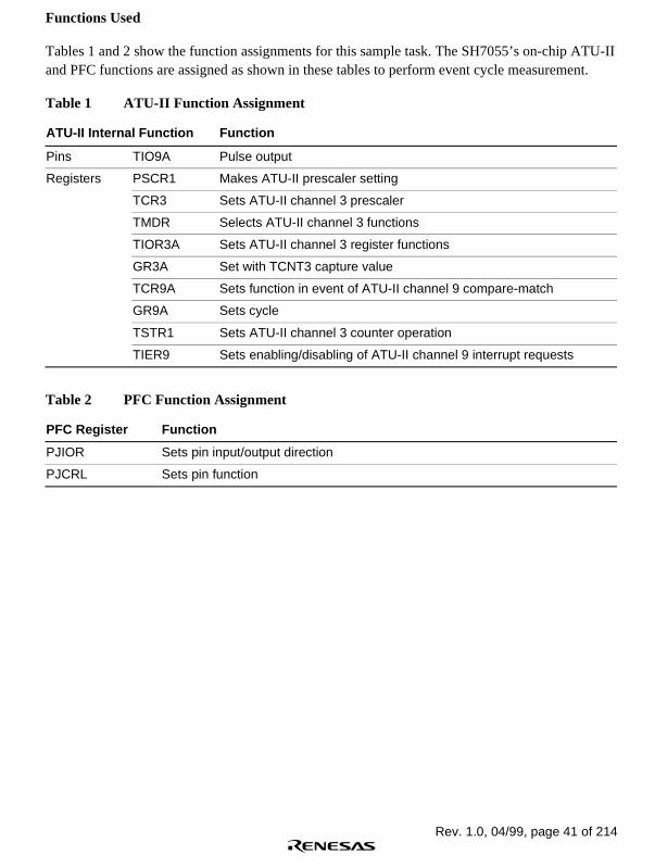
Functions Used
Tables 1 and 2 show the function assignments for this sample task. The SH7055’s on-chip ATU-IIand PFC functions are assigned as shown in these tables to perform event cycle measurement.
Table 1 ATU-II Function Assignment
ATU-II Internal Function Function
Pins TIO9A Pulse output
Registers PSCR1 Makes ATU-II prescaler setting
TCR3 Sets ATU-II channel 3 prescaler
TMDR Selects ATU-II channel 3 functions
TIOR3A Sets ATU-II channel 3 register functions
GR3A Set with TCNT3 capture value
TCR9A Sets function in event of ATU-II channel 9 compare-match
GR9A Sets cycle
TSTR1 Sets ATU-II channel 3 counter operation
TIER9 Sets enabling/disabling of ATU-II channel 9 interrupt requests
Table 2 PFC Function Assignment
PFC Register Function
PJIOR Sets pin input/output direction
PJCRL Sets pin function

Rev. 1.0, 04/99, page 42 of 214
Operation
Figure 2 shows the principles of the operation. Event cycle measurement is performed by meansof SH7055 hardware and software processing, as shown in this figure.
External edge
ECNT9A
TCNT3A
GR3A
GR9A
Hardware processing
Software processing
1. GR3A → RAM2. Use current value as
previous value in next measurement
1. Upon CMI9A generation, the trigger is transmitted to channel 3
Hardware processing
Software processing
1. GR3A – RAM → event cycle2. Use current value as
previous value in next measurement
1. Upon CMI9A generation, the trigger is transmitted to channel 3
Figure 2 Principles of Event Cycle Measurement Operation

Rev. 1.0, 04/99, page 43 of 214
Software
1. Modules
Module Name Label Function
Main routine main Performs ATU-II and RAM initialization
Event cyclemeasurement routine
CVI9A Initiated by CVF9A; performs event cycle measurement
2. Variables Used
Label Function Data Length Module
work Stores captured value
data Stores result of event cycle computation
Unsigned short Event cyclemeasurementroutine
3. Internal Registers Used
Register Name Function Set Value Module
PJ. PJIOR Sets PJ10 as input pin 0x0000
PJ. PJCRH Sets PJ10 pin multiplexing to TI9A 0x0010
ATUC. PACR1 Sets Pø/5 for ATU-II prescaler 1st stage 0x04
ATU3. TCR3 Sets ø'/16 for ATU-II channel 3 prescaler 0x04
ATU3. TMDR Sets IC/OC function for ATU-II channel 3 0x00
ATU3. TIOR3A Sets disabling of ATU-II channel 3 inputcapture
0x04
ATU9. TCR9A Sets transmission of trigger to channel 3 inevent of ATU-II channel 9 compare-match
0x05
ATU9. GR9A Sets cycle 0x03
ATUC. TSTR1 Sets ATU-II channel 3 count start 0x10
ATU9. TIER9 Sets interrupt request by ATU-II channel 3CMF9A
0x0001
INTC. IPRI Sets ATU91 interrupt priority level to 15 0xF000
Main routine
ATU3. GR3A Set with TCNT3 capture value — Event cyclemeasurementroutine

Rev. 1.0, 04/99, page 44 of 214
Program List
/*************************************************************************//* Event Cycle Measurement *//*************************************************************************/#include <machine.h> /* Library function header file */#include "7055.h" /* Peripheral register definition header file *//*************************************************************************//* Function protocol declaration *//*************************************************************************/void main(void);/*************************************************************************//* Variable definitions *//*************************************************************************/#define work (*(unsigned short *)0xFFFFC000) /* Work register */#define data (*(unsigned short *)0xFFFFC002) /* Data storage register *//*************************************************************************//* Main routine *//*************************************************************************/void main(void) PJ.PJCRH = 0x0010; /* TI9A function selection */ PJ.PJIOR = 0x0000; /* Set PJ10 as input pin */ ATUC.PSCR1 = 0x04; /* Prescaler 1st stage: Pø/5 (250 ns) */ ATU3.TCR3 = 0x04; /* Prescaler 2nd stage: ø'/16 (4 µs) */ ATU3.TMDR = 0x00; /* Select IC/OC function */ ATU3.TIOR3A = 0x04; /* Disable input capture: TIO3A */ ATU9.TCR9A = 0x05; /* Count on A rising edge, enable ch3 trigger */ ATU9.GR9A = 0x03; /* Compare-match at 3 count */ ATUC.TSTR1 = 0x10; /* Start channel 3 counter */ ATU9.TIER9 = 0x0001; /* Enable interrupt request by CMF9A */ INTC.IPRI = 0xF000; /* Set ATU91 interrupt level */ set_imask(0x0); /* Enable interrupts */ while(1); /* Endless loop (wait for interrupt) *//*************************************************************************//* Event cycle measurement routine *//*************************************************************************/#pragma interrupt(CVI9A)void CVI9A(void) ATU9.TSR9 &= 0xFFFE; /* Clear compare-match flag 9A */ data = ATU3.GR3A - work; /* Event cycle calculation */ work = ATU3.GR3A; /* Store captured value */

Rev. 1.0, 04/99, page 45 of 214
2.8 Pulse Output
Pulse Output (Toggled Output) MCU: SH7055 Functions Used: ATU-II
Specifications
1. Output is toggled in a fixed cycle, as shown in figure 1.
Output
High output Low output
Figure 1 Toggled Output
Functions Used
Tables 1 and 2 show the function assignments for this sample task. The SH7055’s on-chip ATU-IIand PFC functions are assigned as shown in these tables to perform pulse output.
Table 1 ATU-II Function Assignment
ATU-II Internal Function Function
Pins TIO11A,TIO11B
Pulse output
Registers PSCR1 Makes ATU-II prescaler setting
TCR11 Sets ATU-II channel 11 prescaler
TIOR11 Sets ATU-II channel 11 register functions
GR11A Sets cycle
TSTR3 Sets ATU-II channel 11 counter operation
TIER11 Sets enabling/disabling of ATU-II channel 11 interrupt requests
Table 2 PFC Function Assignment
PFC Register Function
PLIOR Sets pin input/output direction
PLCRL Sets pin function

Rev. 1.0, 04/99, page 46 of 214
Operation
Figure 2 shows the principles of the operation. Pulses are output by means of SH7055 hardwareand software processing, as shown in this figure.
Pulse
TCNT11 value
GR11A
GR11A
GR11A
0x0000
Hardware processing
Software processing
1. Set next compare-match value in GR11A
1. IMI11A generation2. Toggled output from
TIO11A
Hardware processing
Software processing
1. Set next compare-match value in GR11A
1. IMI11A generation2. Toggled output from
TIO11A
Figure 2 Principles of Pulse Output Operation

Rev. 1.0, 04/99, page 47 of 214
Software
1. Modules
Module Name Label Function
Main routine main Performs ATU-II initialization
Compare-matchinterrupt routine
IMI11A Initiated by IMF11A; performs GR11A setting
2. Variables Used
This task does not use any variables.
3. Internal Registers Used
Register Name Function Set Value Module
PL. PLIOR Sets PL1, PL2 as output pins 0x0006
PL. PLCRL Sets PL1, PL2 pin multiplexing to TIO11A,TIO11B
0x003C
ATUC. PSCR1 Sets Pø/2 for ATU-II prescaler 1st stage 0x02
ATU11. TCR11 Sets ø'/2 for ATU-II channel 11 prescaler 0x01
ATU11. TIOR11 Sets ATU-II channel 11 toggled output atcompare-match
0x03
ATUC. TSTR3 Sets ATU-II channel 11 count start 0x01
ATU11. TIER11 Sets enabling of interrupt request by ATU-IIchannel 11 IMF11A
0x0001
INTC. IPRJ Sets ATU11 interrupt priority level to 15 0xF000
Main routine
ATU11. GR11A Sets cycle 0x0064 Compare-match interrupt

Rev. 1.0, 04/99, page 48 of 214
Program List
/************************************************************************//* Pulse Output *//************************************************************************/#include <machine.h> /* Library function header file */#include "7055.h" /* Peripheral register definition header file *//************************************************************************//* Function protocol declaration *//************************************************************************/void main( void );/************************************************************************//* Main routine *//************************************************************************/void main( void ) PL.PLIOR = 0x0006; /* Port L input/output setting */ PL.PLCRL = 0x0014; /* TIO11A, TIO11B (PL1, PL2) */ ATUC.PSCR1 = 0x02; /* Prescaler 1st stage: Pø/2 (100 ns) */ ATU11.TCR11 = 0x01; /* Prescaler 2nd stage: ø'/2 (200 ns) */ ATU11.TIOR11 = 0x03; /* Output toggled at GR11A compare-match */ ATU11.GR11A=0x0064; /* Invert every 20 µs */ ATUC.TSTR3 = 0x01; /* Start channel 11 count */ ATU11.TIER11 = 0x0001; /* Enable interrupt by compare-match IMF11A */ INTC.IPRJ = 0xF000; /* Set ATU11 interrupt priority level to 15 */ set_imask(0x0); /* Enable interrupts */ while(1); /* Endless loop (wait for interrupt) *//************************************************************************//* Compare-match interrupt routine *//************************************************************************/#pragma interrupt( IMI11A )void IMI11A( void ) ATU11.TSR11 &= 0xFE; /* Clear compare-match flag 11A */ ATU11.GR11A += 0x0064; /* Invert every 20 µs */

Rev. 1.0, 04/99, page 49 of 214
2.9 Pulse Output
Pulse Output MCU: SH7055 Functions Used: ATU-II
Specifications
1. Pulses are output with high and low levels repeated in a fixed cycle, as shown in figure 1.
High output Low output
Figure 1 Pulse Output Timing
Functions Used
Tables 1 and 2 show the function assignments for this sample task. The SH7055’s on-chip ATU-IIand PFC functions are assigned as shown in these tables to perform PWM output.
Table 1 ATU-II Function Assignment
ATU-II Internal Function Function
Pins TIO3A–TIO3D Pulse output
Registers PSCR1 Makes ATU-II prescaler setting
TCR3 Sets ATU-II channel 3 prescaler
TSTR Sets ATU-II channel 3 counter operation
TMDR Selects ATU-II channel 3 functions
GR3A Sets PWM cycle
Table 2 PFC Function Assignment
PFC Register Function
PAIOR Sets pin input/output direction
PACRL Sets pin function

Rev. 1.0, 04/99, page 50 of 214
Operation
Figure 2 shows the principles of the operation. Pulses are output by means of SH7055 hardwareand software processing, as shown in this figure.
Pulse
TCNT3 value
GR3A
0x0000
Hardware processing
Software processing
1. Set next compare-match value in GR3ASet output to low level
1. IMI3A generation2. High output from TIO3A
Hardware processing
Software processing
1. Set next compare-match value in GR3ASet output to high level
1. IMI3A generation2. Low output from TIO3A
Figure 2 Principles of PWM Output Operation

Rev. 1.0, 04/99, page 51 of 214
Software
1. Modules
Module Name Label Function
Main routine main Performs ATU-II initialization
Pulse output routine IMI3A Initiated by IMF3A; performs TIOR3A setting
2. Variables Used
This task does not use any variables.
3. Internal Registers Used
Register Name Function Set Value Module
PA. PAIOR Sets PA4–PA7 as output pins 0x00F0
PA. PACRL Sets pin multiplexing to TIO3A–TIO3D 0x5500
ATUC. PSCR1 Sets Pø/2 for ATU-II prescaler 1st stage 0x01
ATU3. TCR3 Sets ø'/2 for ATU-II channel 3 prescaler 0x01
ATU3. TMDR Sets IC/OC function for ATU-II channel 3 0x00
Main routine
ATU3. TIOR3A Sets clearing of TCNT and 1 output at ATU-IIchannel 3 compare-match
0x0A Main routine
Pulse outputroutine
ATU3. GR3A Sets cycle 0x00C8
ATUC. TSTR1 Sets ATU-II channel 3 count start 0x10
ATU3. TIER3 Enables interrupt request by ATU-II channel 3compare-match
0x0001
INTC. IPRF Sets ATU31 interrupt priority level to 15 0xF000
Main routine

Rev. 1.0, 04/99, page 52 of 214
Program List
/************************************************************************//* Pulse Output (Alternating High/Low Output) *//************************************************************************/#include <machine.h> /* Library function header file */#include "7055.h" /* Peripheral register definition header file *//************************************************************************//* Function protocol declaration *//************************************************************************/void main(void);/************************************************************************//* Main routine *//************************************************************************/void main(void) PA.PAIOR = 0x00F0; /* Port A input/output setting */ PA.PACRL = 0x5500; /* TIO3A-TIO3D (PA4-PA7) */ ATUC.PSCR1 = 0x01; /* Prescaler 1st stage: Pø/2 (100 ns) */ ATU3.TCR3 = 0x01; /* Prescaler 2nd stage: ø'/2 (200 ns) */ ATU3.TMDR = 0x00; /* Select IC/OC function */ ATU3.TIOR3A = 0x0A; /* TCNT cleared and 1 output at compare-match */ ATU3.GR3A = 0x00C8; /* Cycle = 40 µs */ ATUC.TSTR1 = 0x10; /* Start channel 3 counter */ ATU3.TIER3 = 0x0001; /* Enable interrupt by compare-match */ INTC.IPRF = 0xF000; /* Set ATU31 interrupt priority level to 15*/ set_imask(0x0); /* Enable interrupts */ while(1); /* Endless loop (wait for interrupt) *//************************************************************************//* Pulse output routine *//************************************************************************/#pragma interrupt(IMI3A)void IMI3A(void) ATU3.TSR3 &= 0xFFFE; /* Clear compare-match interrupt flag */ if (ATU3.TIOR3A == 0x0A) /* 1 output? */ ATU3.TIOR3A = 0x09; /* 0 output at next compare-match */ else ATU3.TIOR3A = 0x0A; /* 1 output at next compare-match */

Rev. 1.0, 04/99, page 53 of 214
2.10 Pulse Output (Toggled Output)
Pulse Output (Toggled Output) MCU: SH7055 Functions Used: ATU-II
Specifications
1. Output is toggled in a fixed cycle, as shown in figure 1.
Output
High output Low output
Figure 1 Toggled Output
Functions Used
Tables 1 and 2 show the function assignments for this sample task. The SH7055’s on-chip ATU-IIand PFC functions are assigned as shown in these tables to perform pulse cycle measurement.
Table 1 ATU-II Function Assignment
ATU-II Internal Function Function
Pins TIO3A–TIO3D Toggled output
PSCR1 Makes ATU-II prescaler setting
TCR3 Makes ATU-II channel 3 prescaler setting
TIOR3A, TIOR3B Select ATU-II channel 3 register functions
TSTR1 Sets ATU-II channel 3 counter operation
TMDR Selects ATU-II channel 3 functions
Registers
GR3A–GR3D Set cycle
Table 2 PFC Function Assignment
PFC Register Function
PAIOR Selects pin input/output direction
PACRL Selects pin function

Rev. 1.0, 04/99, page 54 of 214
Operation
Figure 2 shows the principles of the operation. Toggled output measurement is performed bymeans of SH7055 hardware and software processing, as shown in this figure.
GR3A–GR3D
TCNT3 value
TIO3A
TIO3B
TIO3C
TIO3D
0x0000
Hardware processing
Software processing
None
1. Compare-match generation
2. Clear TCNT3. Toggled output
Hardware processing
Software processing
None
1. Compare-match generation
2. Clear TCNT3. Toggled output
Figure 2 Principles of Toggled Output Operation

Rev. 1.0, 04/99, page 55 of 214
Software
1. Modules
Module Name Label Function
Main routine main Performs ATU-II initialization
2. Variables Used
This task does not use any variables.
3. Internal Registers Used
Register Name Function Set Value Module
PA. PAIOR Sets TIO3A–TIO3D as output pins 0x00F0
PA. PACRL Sets pin multiplexing to use of TIO3A–TIO3D
0x5500
ATUC. PSCR1 Sets Pø/2 for ATU-II prescaler 1st stage 0x01
ATU3. TCR3 Sets ø'/2 for ATU-II channel 3 prescaler 0x01
ATU3. TMDR Sets IC/OC function for ATU-II channel 3 0x00
ATU3. TIOR3A, 3B Sets clearing of TCNT and toggled outputat ATU-II channel 3 compare-match
0xBB
ATUC. TSTR3 Sets ATU-II channel 3 count start 0x10
ATU3. GR3A–GR3D Set cycle 0x00C8
Main routine

Rev. 1.0, 04/99, page 56 of 214
Program List
/************************************************************************//* Pulse Output (Toggled Output) *//************************************************************************/#include <machine.h> /* Library function header file */#include "7055.h" /* Peripheral register definition header file *//************************************************************************//* Function protocol declaration *//************************************************************************/void main(void);/************************************************************************//* Main routine *//************************************************************************/void main(void) PA.PAIOR = 0x00F0; /* Port A input/output setting */ PA.PACRL = 0x5500; /* TIO3A-TIO3D (PA4-PA7) */ ATUC.PSCR1 = 0x01; /* Prescaler 1st stage: Pø/2 (100 ns) */ ATU3.TCR3 = 0x01; /* Prescaler 2nd stage: ø'/2 (200 ns) */ ATU3.TMDR = 0x00; /* Select IC/OC function */ ATU3.TIOR3A = 0xBB; /* TCNT cleared and output toggled at compare-match */ ATU3.TIOR3B = 0xBB; /* TCNT cleared and output toggled at compare-match */ ATU3.GR3A = 0x00C8; /* Cycle = 80 µs */ ATU3.GR3B = 0x00C8; /* Cycle = 80 µs */ ATU3.GR3C = 0x00C8; /* Cycle = 80 µs */ ATU3.GR3D = 0x00C8; /* Cycle = 80 µs */ ATUC.TSTR1 = 0x10; /* Start channel 3 counter */ while(1); /* Endless loop (wait for interrupt) */

Rev. 1.0, 04/99, page 57 of 214
2.11 One-Shot Pulse Output (with Offset)
One-Shot Pulse Output (with Offset) MCU: SH7055 Functions Used: ATU-II
Specifications
1. A one-shot pulse is output in synchronization with the rise of an external signal, as shown infigure 1. An internal clock count value is set for the offset and the pulse width.
2. The offset from the rise of the external signal and the pulse width can be varied within thefollowing ranges:
Pø cycle × 1 < offset < Pø cycle × 65536*
200 ns ≤ pulse width < 13 ms
Note: * The offset must be shorter than the external signal cycle.
Offset Pulse width
One-shot pulse 2
External signal (rising edge) input
One-shot pulse 1
One-shot pulse 8
Figure 1 One-Shot Pulse Output

Rev. 1.0, 04/99, page 58 of 214
Functions Used
Tables 1 and 2 show the function assignments for this sample task. The SH7055’s on-chip ATU-IIand PFC functions are assigned as shown in these tables to perform one-shot pulse output.
Table 1 ATU-II Function Assignment
ATU-II Internal Function Function
TIøA External signal inputPins
TO8A–TO8H One-shot pulse output
PSCR1 Makes ATU-II prescaler 1st stage setting
TCR1A Makes ATU-II prescaler 2nd stage setting
TCR8 Makes ATU-II prescaler 2nd stage setting
TIOR1A–TIOR1D Set ATU-II channel 1 register functions
TRGMDR1 Selects whether compare-match is used as channel 8 one-shot pulse trigger or as terminate trigger
TIER0 Sets enabling/disabling of ATU-II channel 0 interrupt requests
TSTR1 Sets ATU-II channel 0, 1A, 1B counter operation
TCNR Sets enabling/disabling of connection between DST8A–DST8H and down-count start trigger
OSBR Used for detection of counter value at rise of external signal
GR1A–GR1H Make one-shot pulse offset settings
Registers
DCNT8A–DCNT8H Set one-shot pulse widths
Table 2 PFC Function Assignment
PFC Register Function
PAIOR Sets pin input/output direction
PACRL Sets pin function
PKIOR Sets pin input/output direction
PKCRL Sets pin function

Rev. 1.0, 04/99, page 59 of 214
Operation
Figure 2 shows the principles of the operation. One-shot pulse output is performed by means ofSH7055 hardware and software processing, as shown in this figure.
Hardware processing
Software processing
1. Transfer TCNT1 to OSBR12. ICI0A generation
1. OSBR1 + ofset → GR1A–GR1H
2. puls_w → DCNT8A– DCNT8H
Hardware processing
Software processing
1. Set start bit 2. Start DCNT8A–DCNT8H
count3. Output high level from
TO8A–TO8H
None
Hardware processing
Software processing
1. Stop DCNT8A–DCNT8H count
2. Clear start bit3. Output low level from
TO8A–TO8H
None
External signal
TO8A
TO8B
GA1A–GR1H
OSBR1TCNT1
DCNT8A–DCNT8H
TO8C
TO8D
TO8E
TO8F
TO8G
TO8H
Figure 2 Principles of One-Shot Pulse Output Operation

Rev. 1.0, 04/99, page 60 of 214
Software
1. Modules
Module Name Label Function
Main routine main Performs ATU-II and RAM initialization
One-shot pulse output ICI0A Sets offset and pulse width in GR1A–GR1H and DCNT8A–DCNT8H, and outputs one-shot pulse
2. Variables Used
Label Function Data Length Module
ofset Setting of timer value corresponding to one-shotpulse offset
Offset is found from the following formula:
Offset = timer value × Pø cycle × 4 (prescaler scalingfactor)
Unsigned short
puls_w Setting of timer value corresponding to one-shotpulse width
Pulse width is found from the following formula:
Pulse width (ns) =timer value × Pø cycle (50 ns at 20 MHz operation)
× 4 (prescaler scaling factor)
Unsigned short
Main routine
One-shot pulseoutput

Rev. 1.0, 04/99, page 61 of 214
3. Internal Registers Used
Register Name Function Set Value Module
PA. PAIOR Sets PA1 as input 0x0000
PA. PACRL Sets pin multiplexing to TIøA use 0x0001
PK. PKIOR Sets port K as output port 0xFFFF
PK. PKCRL Sets pin multiplexing to TO8A–TO8H use 0x5555
ATUC. PSCR1 Sets Pø/2 for ATU-II prescaler 1st stage 0x01
ATU1. TCR1A Sets ø'/2 for ATU-II channel 1 prescaler2nd stage
0x01
ATU8. TCR8 Sets ø'/2 for ATU-II channel 8 prescaler2nd stage
0x01
ATU0. TIOR0 Sets input capture into ICR0A at TIøArising edge
0x01
ATU1. TIOR1A Sets ATU-II channel 1 GR1A, GR1B forcompare-match use
0x22
ATU1. TIOR1B Sets ATU-II channel 1 GR1C, GR1D forcompare-match use
0x22
ATU1. TIOR1C Sets ATU-II channel 1 GR1E, GR1F forcompare-match use
0x22
ATU1. TIOR1D Sets ATU-II channel 1 GR1G, GR1H forcompare-match use
0x22
ATU1. TRGMDR1 Sets GR1A–GR1H compare-matches forone-shot pulse trigger use
0x80
ATU8. TCNR Enables down-count start trigger A–Hconnection
0x00FF
ATUC. TSTR1 Sets ATU-II channel 0, channel 1 countstart
0x03
ATU0. TIER0 Enables interrupt request by ATU-IIchannel 0 ICF0A
0x01
INTC. IPRC Sets ATU02 interrupt priority level to 15 0x000F
Main routine
ATU1. OSBR1 Used for transfer of TCNT1 at ATU-IIchannel 0A input capture
—
ATU1. GR1A–GR1H Set one-shot pulse offsets —
ATU8. DCNT8A–DCNT8H
Set one-shot pulse widths —
One-shot pulseoutput

Rev. 1.0, 04/99, page 62 of 214
Program List
/************************************************************************//* One-Shot Pulse with Offset *//************************************************************************/#include "machine.h" /* Library function header file */#include "7055.h" /* Peripheral register definition header file *//************************************************************************//* Function protocol declaration *//************************************************************************/void main( void );/************************************************************************//* Variable definitions *//************************************************************************/#define ofset (*(unsigned short *)0xFFFFC000) /* Offset */#define puls_w (*(unsigned short *)0xFFFFC002) /* Pulse width *//************************************************************************//* Main routine *//************************************************************************/void main( void ) PA.PAIOR = 0x0000; /* Port A input/output setting */ PA.PACRL = 0x0001; /* TIøA (PA0) */ PK.PKIOR = 0xFFFF; /* Set port K as output port */ PK.PKCRL = 0x5555; /* TO8H-TO8A (PK7-PK0) */ ATUC.PSCR1 = 0x01; /* Prescaler 1st stage: Pø/2 (100 ns) */ ATU1.TCR1A = 0x01; /* Prescaler 2nd stage: ø'/2 (200 ns) */ ATU8.TCR8 = 0x01; /* Prescaler 2nd stage: ø'/2 (200 ns) */ ATU0.TIOR0 = 0x01; /* Input capture at TIøA rising edge */ ATU1.TIOR1A = 0x22; /* Compare-match function selection (GR1A, GR1B) */ ATU1.TIOR1B = 0x22; /* Compare-match function selection (GR1C, GR1D) */ ATU1.TIOR1C = 0x22; /* Compare-match function selection (GR1E, GR1F) */ ATU1.TIOR1D = 0x22; /* Compare-match function selection (GR1G, GR1H) */ ATU1.TRGMDR1 = 0x80; /* One-shot start trigger (at GR1A-GR1H output compare)*/ ATU8.TCNR = 0x00FF; /* Enable down-counter start trigger A-H connection */ ATUC.TSTR1 = 0x03; /* Start TCNT0, TCNT1A */ ofset = 0x0040; /* Offset = 25.6 µs */ puls_w = 0x0400; /* Pulse width = 409.6 µs */ ATU0.TIER0 = 0x01; /* Enable interrupt by ICF0A */ INTC.IPRC = 0x000F; /* Set ATU02 interrupt priority level to 15 */ set_imask(0x0); /* Enable interrupts */ while(1); /* Endless loop (wait for interrupt) */

Rev. 1.0, 04/99, page 63 of 214
/************************************************************************//* One-shot pulse output routine *//************************************************************************/#pragma interrupt( ICI0A )void ICI0A( void ) ATU0.TSR0 &= 0xFE; /* Clear input capture 0A interrupt flag */ ATU1.GR1A = ATU1.OSBR1 + ofset; /* Offset setting: 25.6 µs */ ATU1.GR1B = ATU1.OSBR1 + ofset; /* Offset setting: 25.6 µs */ ATU1.GR1C = ATU1.OSBR1 + ofset; /* Offset setting: 25.6 µs */ ATU1.GR1D = ATU1.OSBR1 + ofset; /* Offset setting: 25.6 µs */ ATU1.GR1E = ATU1.OSBR1 + ofset; /* Offset setting: 25.6 µs */ ATU1.GR1F = ATU1.OSBR1 + ofset; /* Offset setting: 25.6 µs */ ATU1.GR1G = ATU1.OSBR1 + ofset; /* Offset setting: 25.6 µs */ ATU1.GR1H = ATU1.OSBR1 + ofset; /* Offset setting: 25.6 µs */ ATU8.DCNT8A = puls_w; /* Pulse width setting: 409.6 µs */ ATU8.DCNT8B = puls_w; /* Pulse width setting: 409.6 µs */ ATU8.DCNT8C = puls_w; /* Pulse width setting: 409.6 µs */ ATU8.DCNT8D = puls_w; /* Pulse width setting: 409.6 µs */ ATU8.DCNT8E = puls_w; /* Pulse width setting: 409.6 µs */ ATU8.DCNT8F = puls_w; /* Pulse width setting: 409.6 µs */ ATU8.DCNT8G = puls_w; /* Pulse width setting: 409.6 µs */ ATU8.DCNT8H = puls_w; /* Pulse width setting: 409.6 µs */

Rev. 1.0, 04/99, page 64 of 214
2.12 One-Shot Pulse Output (Terminate)
One-Shot Pulse Output (Terminate) MCU: SH7055 Functions Used: ATU-II
Specifications
1. A one-shot pulse is output in synchronization with the rise of an external signal, as shown infigure 1. An internal clock count value is set for the offset and the pulse width.
2. Pulse output is forcibly terminated and the pulse width controlled by means of settings inOTR.
3. The offset from the rise of the external signal and the pulse width can be varied within thefollowing ranges:
Pø cycle × 1 < offset < Pø cycle × 65536*
200 ns ≤ pulse width < 13.1 ms
Note: * The offset must be shorter than the external signal cycle.
External signal (rising edge) input
Down-counter
One-shot pulse
Offset Pulse width
Figure 1 One-Shot Pulse Output

Rev. 1.0, 04/99, page 65 of 214
Functions Used
Tables 1 and 2 show the function assignments for this sample task. The SH7055’s on-chip ATU-IIand PFC functions are assigned as shown in these tables to perform one-shot pulse output.
Table 1 ATU-II Function Assignment
ATU-II Internal Function Function
TIøA External signal inputPins
TO8I–TO8P One-shot pulse output
Registers PSCR1 Makes ATU-II prescaler 1st stage setting
TCR2A,TCR2B
Make ATU-II prescaler 2nd stage setting
TCR8 Makes ATU-II prescaler 2nd stage setting
TIOR0 Sets ATU-II channel 0 register functions
TIER0 Sets enabling/disabling of ATU-II channel 0 interrupt requests
TIOR2A,TIOR2B
Set ATU-II channel 2 register functions
TCNR Sets enabling/disabling of connection between DST8A–DST8H anddown-count start trigger
OTR Sets enabling/disabling of forcible termination of one-shot pulses
RLDENR Sets enabling/disabling of RLDR value load into DCNT
TSTR1 Sets ATU-II channel 0, 2 counter operation
OSBR2 Used for detection of counter value at rise of external signal
RLDR8 Makes pulse width setting
GR2A–GR2H Make terminate settings
OCR2A Makes one-shot pulse offset setting
Table 2 PFC Function Assignment
PFC Register Function
PAIOR Sets pin input/output direction
PACRL Sets pin function
PKIOR Sets pin input/output direction
PKCRH Sets pin function

Rev. 1.0, 04/99, page 66 of 214
Operation
Figure 2 shows the principles of the operation. One-shot pulses are cut off by means of SH7055hardware and software processing, as shown in this figure.
External signal
TCNT2OSBR2
OCR2A–H
DCNT8I–P
TO8I
TO8J
TO8K
TO8L
TO8M
TO8N
TO8O
TO8P
GR2AGR2BGR2CGR2DGR2EGR2FGR2GGR2H
Hardware processing
Software processing
1. Transfer TCNT2 to OSBR22. ICI0A generation
1. OSBR2 + offset → OCR2A–OCR2H
2. plsw setting3. OCR2A–OCR2H + terminate
value → GR2A–GR2H
Hardware processing
Software processing
1. Set start bit2. Start DCNT8I–DCNT8P
count3. Output high level from
TO8I–TO8P
None
Hardware processing
Software processing
1. Output low level from TO8I–TO8P
2. Clear DCNT
None
Figure 2 Principles of One-Shot Pulse Cutoff Operation

Rev. 1.0, 04/99, page 67 of 214
Software
1. Modules
Module Name Label Function
Main routine main Performs ATU-II and RAM initialization
One-shot pulse output ICI0A Makes offset, pulse width, and terminate settings, andperforms one-shot pulse output and cutoff
2. Variables Used
Label Function Data Length Module
ofset Setting of timer value corresponding to one-shotpulse offset
Offset is found from the following formula:
Offset = timer value × Pø cycle × 4 (prescaler scalingfactor)
Unsigned short
plsw Setting of timer value corresponding to one-shotpulse width
Pulse width is found from the following formula:
Pulse width (ns) =timer value × Pø cycle (50 ns at 20 MHz operation)
× 4 (prescaler scaling factor)
Unsigned short
Main routine
One-shot pulseoutput

Rev. 1.0, 04/99, page 68 of 214
3. Internal Registers Used
Register Name Function Set Value Module
PA. PAIOR Sets PA1 as input 0x0000
PA. PACRL Sets pin multiplexing to TIøA use 0x0001
PK. PKIOR Sets port K as output port 0xFFFF
PK. PKCRH Sets pin multiplexing to TO8I–TO8P use 0x5555
ATUC. PSCR1 Sets Pø/2 for ATU-II prescaler 1st stage 0x01
ATU2. TCR2A Sets ø'/2 for ATU-II channel 2 prescaler 2ndstage
0x01
ATU8. TCR8 Sets ø'/2 for ATU-II channel 8 prescaler 2ndstage
0x11
ATU0. TIOR0 Sets input capture into ICRøA at TIøA risingedge
0x01
ATU2. TIOR2A Sets ATU-II channel 2 GR2A, GR2B forcompare-match use
0x11
ATU2. TIOR2B Sets ATU-II channel 2 GR2C, GR2D forcompare-match use
0x11
ATU2. TIOR2C Sets ATU-II channel 2 GR2E, GR2F forcompare-match use
0x11
ATU2. TIOR2D Sets ATU-II channel 2 GR2G, GR2H forcompare-match use
0x11
ATU8. TCNR Enables down-counter start trigger I–Pconnection
0xFF00
ATU8. OTR Enables forcible termination by down-counterterminate trigger I–P
0xFF00
ATUC. TSTR1 Sets ATU-II channel 0, channel 2 count start 0x0D
ATU8. RLDENR Enables load of RLDR value into down-counter 0x80
ATU0. TIER0 Enables interrupt request by ATU-II channel 0ICF0A
0x01
INTC. IPRC Sets ATU02 interrupt priority level to 15 0x000F
Main routine
ATU2. OSBR2 Sets TCNT2 at ATU-II channel 0 input capture —
ATU2. OCR2A–OCR2H
Set one-shot pulse offsets —
ATU8. RLDR8 Sets one-shot pulse width —
ATU2. GR2A–GR2H
Set terminate values —
One-shot pulseoutput

Rev. 1.0, 04/99, page 69 of 214
Program List
/************************************************************************//* One-Shot Pulse Output with Offset (Terminate) *//************************************************************************/#include <machine.h> /* Library function header file */#include "7055.h" /* Peripheral register definition header file *//************************************************************************//* Function protocol declaration *//************************************************************************/void main( void );/************************************************************************//* Variable definitions *//************************************************************************/#define ofset (*(unsigned short *)0xFFFFC000) /* Offset */#define plsw (*(unsigned short *)0xFFFFC002) /* Pulse width *//************************************************************************//* Main routine *//************************************************************************/void main( void ) PA.PAIOR = 0x0000; /* Port A input/output setting */ PA.PACRL = 0x0001; /* TIøA (PA0) */ PK.PKIOR = 0xFFFF; /* Set port K as output port */ PK.PKCRH = 0x5555; /* TO8P-TO8I (PK15-PK8) */ ATUC.PSCR1 = 0x01; /* Prescaler 1st stage: Pø/2 (100 ns) */ ATU2.TCR2A = 0x01; /* Prescaler 2nd stage: ø'/2 (200 ns) */ ATU2.TCR2B = 0x01; /* Prescaler 2nd stage: ø'/2 (200 ns) */ ATU8.TCR8 = 0x11; /* Prescaler 2nd stage: ø'/2 (200 ns) */ ATU0.TIOR0 = 0x01; /* Input capture at TIøA rising edge */ ATU0.TIER0 = 0x01; /* Enable interrupt by ICF0A */ ATU2.TIOR2A = 0x11; /* GR2A, GR2B compare-match function */ ATU2.TIOR2B = 0x11; /* GR2C, GR2D compare-match function */ ATU2.TIOR2C = 0x11; /* GR2E, GR2F compare-match function */ ATU2.TIOR2D = 0x11; /* GR2G, GR2H compare-match function */ ATU8.TCNR = 0xFF00; /* Enable down-counter start trigger A-H connection */ ATU8.OTR = 0xFF00; /* Enable forcible termination by down-counter terminate trigger A-H */ ATU8.RLDENR = 0x80; /* Enable load of reload register value into down-counter */ ATUC.TSTR1 = 0x0D; /* Start TCNT0, TCNT2A, TCNT2B */ ofset = 0x0040; /* Offset = 12.8 µs */ plsw = 0x0400; /* Pulse width = 204.8 µs */ INTC.IPRC = 0x000F;/* Set ATU02 interrupt priority level to 15 */ set_imask(0x0); /* Enable interrupts */ while(1); /* Endless loop (wait for interrupt)*/

Rev. 1.0, 04/99, page 70 of 214
/************************************************************************//* One-shot pulse output routine *//************************************************************************/#pragma interrupt( ICI0A )void ICI0A( void ) ATU0.TSR0 &= 0xFE; /* Clear input capture 0A interrupt flag */ ATU2.OCR2A = ATU2.OSBR2 + ofset /* Offset setting: 12.8 µs */ ATU2.OCR2B = ATU2.OSBR2 + ofset; /* Offset setting: 12.8 µs */ ATU2.OCR2C = ATU2.OSBR2 + ofset; /* Offset setting: 12.8 µs */ ATU2.OCR2D = ATU2.OSBR2 + ofset; /* Offset setting: 12.8 µs */ ATU2.OCR2E = ATU2.OSBR2 + ofset; /* Offset setting: 12.8 µs */ ATU2.OCR2F = ATU2.OSBR2 + ofset; /* Offset setting: 12.8 µs */ ATU2.OCR2G = ATU2.OSBR2 + ofset; /* Offset setting: 12.8 µs */ ATU2.OCR2H = ATU2.OSBR2 + ofset; /* Offset setting: 12.8 µs */ ATU8.RLDR8 = plsw; /* Pulse width setting: 204.8 µs */ ATU2.GR2A = ATU2.OCR2A + 0x0040; /* Terminate after 12.8 µs */ ATU2.GR2B = ATU2.OCR2B + 0x0080; /* Terminate after 25.6 µs */ ATU2.GR2C = ATU2.OCR2C + 0x0100; /* Terminate after 51.2 µs */ ATU2.GR2D = ATU2.OCR2D + 0x0180; /* Terminate after 76.8 µs */ ATU2.GR2E = ATU2.OCR2E + 0x0200; /* Terminate after 102.4 µs */ ATU2.GR2F = ATU2.OCR2F + 0x0280; /* Terminate after 128.0 µs */ ATU2.GR2G = ATU2.OCR2G + 0x0300; /* Terminate after 153.6 µs */ ATU2.GR2H = ATU2.OCR2H + 0x0400; /* Terminate after 204.8 µs */

Rev. 1.0, 04/99, page 71 of 214
2.13 One-Shot Output from Missing-Teeth Detection(Channels 1, 2, 8, 10 Linked)
One-Shot Output from Missing-TeethDetection (Channels 1, 2, 8, 10 Linked)
MCU: SH7055 Functions Used: ATU-II
Specifications
1. Missing teeth and rising edges in the external input signal (two teeth missing out of 16) aredetected, and offset one-shot pulses are output at a fixed timing (phase difference) relative tothe input signal, as shown in figure 1.
2. Halting of external signal input is detected. When input is resumed, the operation is the sameas at startup.
3. This application handles external input signals for which the frequency varies within thefollowing range.
Preceding/following pulse cycle × 0.4 ≤ current pulse cycle < preceding/following pulse cycle× 2.5*
Note: * Missing teeth may not be detected in signals outside this range.
External input signal
One-shot pulse output
OffsetMissing-teeth interval (3 pulse cycles)
Figure 1 One-Shot Pulse Output from Missing-Teeth Output

Rev. 1.0, 04/99, page 72 of 214
Functions and Set Values Used
Tables 1 and 2 show the pin functions and ATU-II function assignments, and set values used inthis sample application.
Table 1 Pin Functions
Pin Functions Set Value Function
PA0 — Cycle decision level (high: 1st cycle, low: 2nd cycle)input pin
PL0 — ATU-II channel 10 external input pin (TI10)
PK0–PK7 — ATU-II channel one-shot pulse output pins (TO8A toTO8H)
Pins
PK8–PK15 — ATU-II channel one-shot pulse output pins (TO8I toTO8P)
PACRL H'0000 Sets PA0 to general I/O pin function
PAIOR H'0000 Sets PA0 as input pin
PADR — Stores PA0 input level
PLCRL H'0001 Sets PL0 to ATU-II channel 10 external input pin function
PLIOR H'0000 Sets PL0 as input pin
PKCRL H'5555 Sets PK0–PK7 to ATU-II channel 8 one-shot pulseoutput pin function
PKCRH H'5555 Sets PK8–PK15 to ATU-II channel 8 one-shot pulseoutput pin function
Registers
PKIOR H'FFFF Sets PK0–PK15 as output pins

Rev. 1.0, 04/99, page 73 of 214
Table 2 ATU-II
ATU-II Set Value Function
Pins TO8A–TO8P — One-shot pulse output pins
TI10 — External input pin
Registers Common TSTR1 H'8E Sets operation of TCNT1A, TCNT1B, TCNT2A,TCNT2B, TCNT10
PSCR1, PSCR4 H'04 Sets Pø/5 for first prescaler
Channel 1 TCR1A, TCR1B H'09 Sets TCNT1A, TCNT1B to count on correction clock(AGCKM)
TIOR1A–TIOR1D H'11 Set GR1A–GR1H to compare-match function
GR1A–GR1H As required Set TO8A–TO8H one-shot pulse offset values
TRGMDR1 H'80 Sets GR1A–GR1H compare-matches as TO8A–TO8H one-shot pulse start triggers
Channel 2 TCR2A, TCR2B H'09 Sets TCNT2A, TCNT2B to count on correction clock(AGCKM)
TIOR2A–TIOR2D H'11 Set GR2A–GR2H to compare-match function
GR2A–GR2H As required Set TO8I–TO8P one-shot pulse terminate values
OCR2A–OCR2H As required Set TO8I–TO8P one-shot pulse offset values
Channel 8 TCR8 H'44 Sets ø'/16 for second prescaler
TCNR H'FFFF Enables connection between ATU-II channel 8down-count start register (DSTR) and channel 1 and2 compare-match signals
OTR H'FF00 Sets enabling of down-counter terminate trigger bycompare-match between TCNT2A and GR2A–GR2H
DCNT8A–DCNT8P As required Set one-shot pulse widths
Channel 10 TCR10 H'F5 Sets TCNT1A, TCNT1B, TCNT2A, TCNT2B clearingwhen TCCLR10 = TCNT10F, enabling of noisecancellation function, TI10 input rising edgedetection
TIOR10 As required*1 Sets RLD10C updating, disables TCNT10E haltingwhen TCNT10D (shift value) = TCNT10E, setsmultiplication factor of 256
TIER10 As required*2 Sets enabling/disabling of interrupts by TSR10 statusflags
OCR10A H'0000FFFF Sets external input TI10 halt detection value(> missing-teeth interval)
OCR10B As required*3 Sets compare-match interrupt to rising edge at every4th tooth in external input TI10
RLD10C H'0013*4 Sets external input TI10 cycle/multiplicationfactor/first prescaler cycle. Updates to[1/multiplication factor] of ICR10A value according toTIOR10 setting (RLDEN = 0)

Rev. 1.0, 04/99, page 74 of 214
Table 2 ATU-II (cont)
ATU-II Set Value Function
Registers Channel 10 TCNT10C H'0001 RLD10C value is transferred when H'0001; countsdown according to first prescaler. Generates scaledclock (AGCK1)
TCNT10D As required*5 Counts on external input TI10; value shiftedaccording to set multiplication factor is transferred toTCNT10E
TCNT10F H'1000 Initial setting = TCCLR10. Generates correctionclock (AGCKM)
TCCLR H'1000 Sets number of correction clocks in cycle (TI10 ×multiplication factor)
GR10G H'0280 Sets TCNT10G missing-teeth detection value(multiplication factor × 2.5)
NCR10 H'FF Masks TI10 input according to set value. Maskcleared when NCR10 = TCNT10H
Notes: 1. As the value of ICR10A is undefined in initialization, RLD10C updating is disabled, and is enabledafter capture.
2. In initialization, and after external input TI10 halt detection (CMI10A), only interrupts by ICF10A areenabled.
After capture (first interrupt by CMF10A), interrupts by CMF10G are enabled.
After missing-teeth detection (interrupt by CMF10G), interrupts by all TSR10 status flags areenabled, but only a one-time interrupt by ICF10A is enabled.
3. After missing-teeth detection, a compare-match interrupt (CMI10B) every 4 teeth for a 16-toothcycle is set.
4. As the initial value is an estimate, if it is undefined, a larger RLD10C value is set. In this case, anumber of cycles may be necessary before missing teeth are detected. If a smaller value is set,missing teeth may be erroneously detected during a normal tooth period, resulting in faultyoperation.
5. TCNT10D requires correction of the missing-teeth interval in a cycle (the number of missing teethare added to TCNT10D by an interrupt at the edge immediately before the missing-teeth interval;this correction is not performed in this sample application) and initialization (to H'00) during themissing-teeth interval at the end of the cycle.

Rev. 1.0, 04/99, page 75 of 214
Operation
Figure 2 shows the principles of the operation. Missing teeth and rising edges in the external inputsignal (two teeth missing out of 16) are detected, offset one-shot pulses are output at a fixedtiming (phase difference) relative to the input, and halting of external signal input is detected bymeans of SH7055 hardware and software processing, as shown in this figure.
GR10G
TCNT10G
TCNT10A
OCR10A
TCNT1A,1B, 2A,2BGR1A,E, OCR2A,E
GR1B,F, OCR2B,F
GR1C,G, OCR2C,G
GR1D,H, OCR2D,H
GR2A,E
GR2B,F
GR2C,G
GR2D,H
TO8A
TO8B
TO8C
TO8D
TO8E
TO8I
TO8J
TO8K
TO8L
TO8M
Hardware processing
Software processing
1. Start count
Hardware processing
Software processing
1. Transfer TCNT10A to ICR10A
2. Clear TCNT10A, TCNT10G
3. Transfer TCNT10D(multiplied) to TCNT10E
* TCNT10D, TCNT10E, TCNT10F cleared by condition TCNT10D = H'00 when TCNT10F = TCCLR
4. IMI10AG generation
1. Enable RLD10C updating
2. Enable interrupts byCMF10G
Hardware processing
Software processing
1. IMI10AG generation
Hardware processing
Software processing
1. CMI10B generation
Hardware processing
Software processing
1. CMI10A generation
1. Initialization 1. Set CYLINDER2. Enable interrupts by
CMF10A, CMF10B3. Clear correction
counter: TCNT10D = H'00
1. Set DCNT8A–DCNT8P, GR1A–GR1H, GR2A–GR2H, OCR2A–OCR2H
2. Update OCR10B3. Update CYLINDER
1. Initialize counters, registers
2. Enable only interrupts by ICF10A
Other hardware processing: Clearing of TCNT1A, TCNT1B, TCNT2A, TCNT2B when TCCLR = TCNT10FOther software processing: Setting of source determination within IMI10AG and enabling/disabling by individual source
Figure 2 Principles of One-Shot Pulse Output from Missing-Teeth Detection

Rev. 1.0, 04/99, page 76 of 214
Software
1. Modules
Module Name Label Function
main Performs ATU-II, interrupt controller, and RAM initialization
port init Performs I/O port initialization
ch1 init Performs ATU-II channel 1 initialization
ch2 init Performs ATU-II channel 2 initialization
ch8 init Performs ATU-II channel 8 initialization
Main routine
ch10 init Performs ATU-II channel 10 initialization
Missing-teeth andedge detection
IMI10AG Detects external input TI10 missing teeth and edge
Edge detection CMI10BINJSETIGNSET
Set offset one-shot pulses output at fixed timing (phasedifference) relative to external input TI10
External signal inputhalt detection
CMI10A Detects halting of external input TI10 signal input, and returnsto initial state

Rev. 1.0, 04/99, page 77 of 214
2. Variables Used
Label FunctionDataLength
LabelUsed
OFFSET [ ] Setting of timer value corresponding to offset ofone-shot pulses output from TO8A–TO8H
Offset is found from the following formula:
Offset = timer value × correction clock (AGCKM)
Unsignedshort
INJSET
INJPULSE [ ] Setting of timer value corresponding to pulse width ofone-shot pulses output from TO8A–TO8H
Pulse width is found from the following formula:
Pulse width (ns) = timer value× Pø cycle (50 ns at 20 MHz operation)× 80 (prescaler scaling factor)
Unsignedshort
INJSET
IPW [ ] Setting of timer value corresponding to pulse width ofone-shot pulses output from TO8I–TO8P
Pulse width is found from the following formula:
Pulse width (ns) = timer value× Pø cycle (50 ns at 20 MHz operation)× 80 (prescaler scaling factor)
Unsignedshort
IGNSET
DWELL [ ] Setting of timer value corresponding to offset of one-shotpulses output from TO8I–TO8P
Offset is found from the following formula:
Offset = timer value × correction clock (AGCKM)
Unsignedshort
IGNSET
IGN [ ] Setting of timer value corresponding to output cutoff(termination) of one-shot pulses output from TO8I–TO8P
Terminate value is found from the following formula:
Terminate value = timer value × correction clock (AGCKM)
Unsignedshort
IGNSET
MISSTEETH Sets status within IMI10AG Unsignedchar
mainIMI10AG
SYLINDER Indicates phase of edge that is CMI10B generation source
Also used as GR1A–GR1H, GR2A–GR2H, OCR2A–OCR2H, and variable address offset.
Unsignedchar
IMI10AGCMI10BCMI10A

Rev. 1.0, 04/99, page 78 of 214
Program List
/*****************************************************************************//* One-Shot Pulse Output from Missing-Teeth Detection*//*****************************************************************************/#include <stdio.h> /* Library function header file */#include <machine.h>#include "7055.h" /* Peripheral register definition header file *//*****************************************************************************//* Function prototype declaration *//*****************************************************************************/void main( void );void port_init(void);void ch1init(void);void ch2init(void);void ch8init(void);void ch10init(void);void INJSET(void);void IGNSET(void);/*****************************************************************************//* Variable definitions *//*****************************************************************************/unsigned short OFFSET[8]=0x0200,0x0600,0x0A00,0x0E00,0x0200,0x0600,0x0A00,0x0E00;unsigned short INJPULSE[]=0x0080;unsigned short IPW[]=0x00A0;unsigned short DWELL[8]=0x0200,0x0600,0x0A00,0x0E00,0x0200,0x0600,0x0A00,0x0E00;unsigned short IGN[8]=0x0280,0x0680,0x0A80,0x0E80,0x0280,0x0680,0x0A80,0x0E80;unsigned char MISSTEETH;unsigned char CYLINDER;/*****************************************************************************//* Main routine *//*****************************************************************************/void main( void ) ATUC.PSCR1 = 0x04; /* Prescaler 1st stage: Pø/5 (250 ns) */ ATUC.PSCR4 = 0x04; /* Prescaler 1st stage: Pø/5 (250 ns) */ port_init(); /* SH7055 I/O port initialization routine */ ch1init(); /* ATU-II CH1 initialization routine */ ch2init(); /* ATU-II CH2 initialization routine */ ch8init(); /* ATU-II CH8 initialization routine */ ch10init(); /* ATU-II CH10 initialization routine */ MISSTEETH = 0x00; /* Clear enable flag in IMI10AG */ ATUC.TSTR1 = 0x8E; /* Start TCNT1A, TCNT1B, TCNT2A, TCNT2B, TCNT10 */ INTC.IPRI = 0x00FF; /* Set interrupt level */ set_imask(0x0); /* Enable interrupts */ while(1); /* Endless loop (wait for interrupt) */

Rev. 1.0, 04/99, page 79 of 214
/*** Port initialization routine ***/void port_init(void) PA.PACRL = 0x0000; /* Set PA0-PA7 to general input/output */ PA.PAIOR = 0x0000; /* Port A input/output setting */ PL.PLIOR = 0x0000; /* Port L input/output setting */ PL.PLCRL = 0x0001; /* Set PL0 to TI10 */ PK.PKIOR = 0xFFFF; /* Port K input/output setting */ PK.PKCRH = 0x5555; /* Set PK8-PK15 to TO8I-TO8P */ PK.PKCRL = 0x5555; /* Set PK0-PK7 to TO8A-TO8H *//*** ATU-II CH1 initialization routine ***/void ch1init(void) ATU1.TIOR1A = 0x11; /* Set GR to compare-match function */ ATU1.TIOR1B = 0x11; ATU1.TIOR1C = 0x11; ATU1.TIOR1D = 0x11; ATU1.TCR1A = 0x09; /* Count on AGCKM rising edge */ ATU1.TCR1B = 0x09; ATU1.TRGMDR1 = 0x80; /* Set GR1A-GR1H compare-matches as one-shot pulse start triggers *//*** ATU-II CH2 initialization routine ***/void ch2init(void) ATU2.TIOR2A = 0x11; /* Set GR to compare-match function */ ATU2.TIOR2B = 0x11; ATU2.TIOR2C = 0x11; ATU2.TIOR2D = 0x11; ATU2.TCR2A = 0x09; /* Count on AGCKM rising edge */ ATU2.TCR2B = 0x09;/*** ATU-II CH8 initialization routine ***/void ch8init(void) ATU8.TCR8 = 0x44; /* Internal clock ø": count on ø'/16 */ ATU8.TCNR = 0xFFFF; /* Enable connection of CH8 DSTR and CH1, CH2 compare-match signals */ ATU8.OTR = 0xFF00; /* Enable forcible termination by I-P down-counter terminate trigger */

Rev. 1.0, 04/99, page 80 of 214
/*** ATU-II CH10 initialization routine ***/void ch10init(void) ATU10.TCR10 = 0xF5; /* TCNT1A, TCNT1B, TCNT2A, TCNT2B clearing when TCCLR10 = TCNT10F Enable noise cancellation function TI10 input rising edge detection */ ATU10.TIOR10 = 0xB1; /* RLD10C update masked, TCNT10E correction disabled AGCKM: count on TI10 clock × 256 */ ATU10.TIER10 = 0x0002; /* Set interrupt enabling/disabling */ ATU10.RLD10C = 0x0013; /* Set initial value */ ATU10.TCNT10C = 0x0001; /* Set initial value */ ATU10.TCCLR10 = 0x1000; /* Number of AGCKM clocks in 1 cycle */ ATU10.TCNT10F = 0x1000; /* Set initial value (= TCCLR10) */ ATU10.TCNT10D = 0x00; /* Set initial value */ ATU10.GR10G = 0x0280; /* Set missing-teeth detection value (multiplication factor × 2.5) */ ATU10.OCR10A = 0x0000FFFF; /* Set TI10 input halt detection value */ ATU10.NCR10 = 0xFF; /* Set noise cancellation interval */

Rev. 1.0, 04/99, page 81 of 214
/*****************************************************************************//* Interrupt Routine *//*****************************************************************************/#pragma interrupt(IMI10AG,CMI10A,CMI10B)void IMI10AG(void) if((ATU10.TSR10 & 0x0008) == 0x0008) /* Interrupt by CMF10G */ if(MISSTEETH != 0x00) ATU10.OCR10B = ATU10.TCNT10B+1; /* OCR10B setting */ if(MISSTEETH == 0x0F) MISSTEETH = 0xF0; ATU10.TIER10 |= 0x0005; /* Enable interrupts by CMF10A, CMF10B */ if((PA.PADR & 0x0001) == 0x0000) /* First cycle */ CYLINDER = 0x00; /* Cylinder number setting 0 */ else /* Second cycle */ CYLINDER = 0x04; /* Cylinder number setting 4 */ ATU10.TCNT10D = 0x00; /* Clear correction counter */ ATU10.TSR10 &= 0xFFF7; /* Clear status flags */ if((ATU10.TSR10 & 0x0002) == 0x0002) /* Interrupt by ICF10A */ if(MISSTEETH != 0xFF) if(MISSTEETH == 0xF0) MISSTEETH = 0xFF; ATU10.TIER10 &= 0xFFFD; /* Disable interrupt by ICF10A */ else MISSTEETH = 0x0F; ATU10.TIOR10 = 0x31; /* Enable RLD10C updating */ ATU10.TIER10 |= 0x0008; /* Enable interrupt by CMF10G */ ATU10.TSR10 &= 0xFFF4; /* Clear status flags */

Rev. 1.0, 04/99, page 82 of 214
void CMI10B(void) /* Interrupt by CMF10B */ INJSET(); /* One-shot pulse A-H setting routine */ IGNSET(); /* One-shot pulse I-P setting routine */ if((CYLINDER & 0x03) == 0x03) /* Cylinder numbers 3, 7 */ ATU10.OCR10B += 0x02; /* Update OCR10B */ else /* Cylinder numbers 0-2, 4-6 */ ATU10.OCR10B += 0x04; /* Update OCR10B */ CYLINDER += 0x01; /* Update cylinder number */ ATU10.TSR10 &= 0xFFFB; /* Clear status flags */void CMI10A(void) /* Interrupt by CMF10A */ ATU10.TIER10 = 0x0002; /* Enable interrupt by ICF10A */ ATU10.RLD10C = 0x0013; /* Set initial value */ ATU10.TCNT10C = 0x0001; /* Set initial value */ ATU10.TCNT10F = 0x1000; /* Set initial value */ MISSTEETH = 0x00; /* Clear missing-teeth detection flag */ ATU10.TSR10 &= 0xFFF0; /* Clear status flags *//*** One-shot pulse A-H setting routine ***/void INJSET(void) *(&ATU8.DCNT8A + CYLINDER) = INJPULSE[0]; /* Set DCNT8A-DCNT8H (pulse width) */ *(&ATU1.GR1A + CYLINDER) = OFFSET[CYLINDER]; /* Set GR1A-GR1H (offset) *//*** One-shot pulse I-P setting routine ***/void IGNSET(void) *(&ATU8.DCNT8I + CYLINDER) = IPW[0]; /* Set DCNT8I-DCNT8P (pulse width) */ *(&ATU2.GR2A + CYLINDER) = IGN[CYLINDER]; /* Set GR2A-GR2H (terminate) */ *(&ATU2.OCR2A + CYLINDER) = DWELL[CYLINDER]; /* Set OCR2A-OCR2H (offset) */

Rev. 1.0, 04/99, page 83 of 214
2.14 PWM Output
PWM Output MCU: SH7055 Functions Used: ATU-II
Specifications
1. Variable-duty/variable-cycle pulses are output as shown in figure 1.
Duty pulse
Pulse cycle
Pulse high width Pulse low width
Duty = Pulse high widthPulse cycle
× 100(%)
Figure 1 PWM Output Timing

Rev. 1.0, 04/99, page 84 of 214
Functions Used
Tables 1 and 2 show the function assignments for this sample task. The SH7055’s on-chip ATU-IIand PFC functions are assigned as shown in these tables to perform PWM output.
Table 1 ATU-II Function Assignment
ATU-II Internal Function Function
Pins TIO3A–TIO3D PWM output
Registers PSCR1 Makes ATU-II prescaler setting
TCR3 Sets ATU-II channel 3 prescaler
TMDR Selects ATU-II channel 3 function
GR3D Sets PWM cycle
GR3A–GR3C Set PWM duty
TSTR1 Sets ATU-II channel 3 counter operation
Table 2 PFC Function Assignment
PFC Register Function
PAIOR Sets pin input/output direction
PACRH Sets pin function

Rev. 1.0, 04/99, page 85 of 214
Operation
Figure 2 shows the principles of the operation. Pulse output is performed by means of SH7055hardware and software processing, as shown in this figure.
GR3D
GR3A
GR3B
GR3C
TCNT3 value
TIO3A
TIO3B
TIO3C
0x0000
Hardware processing
Software processing
None
1. Clear TCNT
Hardware processing
Software processing
None
1. Compare-match generation2. Generate output reflecting
duty value
Figure 2 Principles of PWM Output Operation

Rev. 1.0, 04/99, page 86 of 214
Software
1. Modules
Module Name Label Function
Main routine main Performs ATU-II initialization
2. Variables Used
This task does not use any variables.
3. Internal Registers Used
Register Name Function Set Value Module
PA. PAIOR Sets PA4–PA7 as output pins 0x00F0
PA. PACRL Sets pin multiplexing to pins TIO3A–TIO3D 0x5500
ATUC. PSCR1 Sets Pø/2 for ATU-II prescaler 1st stage 0x01
ATU3. TCR3 Sets ø'/2 for ATU-II channel 3 prescaler 0x01
ATU3. TMDR Selects PWM function for ATU-II channel 3 0x01
ATU3. GR3D Sets cycle 0x6400
ATU3. GR3A Sets duty 0x3200
ATU3. GR3B Sets duty 0x1900
ATU3. GR3C Sets duty 0x0C80
ATUC. TSTR1 Sets ATU-II channel 3 count start 0x10
Main routine

Rev. 1.0, 04/99, page 87 of 214
Program List
/***********************************************************************//* PWM Output *//***********************************************************************/#include <machine.h> /* Library function header file */#include "7055.h" /* Peripheral register definition header file *//***********************************************************************//* Function protocol declaration *//***********************************************************************/void main(void);/***********************************************************************//* Main routine *//***********************************************************************/void main(void) PA.PAIOR = 0x00F0; /* Port A input/output setting */ PA.PACRL = 0x5500; /* TIO3A-TIO3D (PA4-PA7) */ ATUC.PSCR1 = 0x01; /* Prescaler 1st stage: Pø/2 (100 ns) */ ATU3.TCR3 = 0x01; /* Prescaler 2nd stage: ø'/2 (200 ns) */ ATU3.TMDR = 0x01; /* Select PWM function */ ATU3.GR3D = 0x6400; /* Cycle = 10.24 ms */ ATU3.GR3A = 0x3200; /* Duty 1 = 50% */ ATU3.GR3B = 0x1900; /* Duty 2 = 25% */ ATU3.GR3C = 0x0C80; /* Duty 3 = 12.5% */ ATUC.TSTR1 = 0x10; /* Start channel 3 counter */ while(1); /* Endless loop */

Rev. 1.0, 04/99, page 88 of 214
2.15 Noncomplementary PWM Output (Special-Purpose)
Noncomplementary PWM Output(Special-Purpose)
MCU: SH7055 Functions Used: ATU-II
Specifications
1. Variable-duty/variable-cycle pulses are output as shown in figure 1.
2. An output pulse duty of 100% to 0% can be set arbitrarily.
PWM
Pulse cycle
Duty
Duty = Pulse high widthPulse cycle
× 100%
Figure 1 Noncomplementary PWM Output Timing

Rev. 1.0, 04/99, page 89 of 214
Functions Used
Tables 1 and 2 show the function assignments for this sample task. The SH7055’s on-chip ATU-IIand PFC functions are assigned as shown in these tables to perform PWM output.
Table 1 ATU-II Function Assignment
ATU-II Internal Function Function
Pins TO6A–TO6D PWM output
Registers PSCR2 Makes ATU-II prescaler setting
TCR6A, TCR6B Set ATU-II channel 6 prescaler
PMDR6 Sets ATU-II channel 6 PWM output specification
CYLR6A–CYLR6D Set PWM cycle
BFR6A–BFR6D Set PWM duty
TSTR2 Sets ATU-II channel 6A–6D counter operation
TIER6 Sets enabling/disabling of ATU-II channel 6 interrupt requests
Table 2 PFC Function Assignment
PFC Register Function
PBIOR Sets pin input/output direction
PBCRL Sets pin function

Rev. 1.0, 04/99, page 90 of 214
Operation
Figure 2 shows the principles of the operation. Pulse output is performed by means of SH7055hardware and software processing, as shown in this figure.
CYLR6A–DBFR6A
BFR6B
BFR6C
BFR6D
TCNT6A–6D
TO6A
TO6B
TO6C
TO6D
0x0000
Hardware processing
Software processing
1. Set duty in BFR
1. Compare-match generation2. Output reflecting duty value
Figure 2 Principles of Noncomplementary PWM Output Operation

Rev. 1.0, 04/99, page 91 of 214
Software
1. Modules
Module Name Label Function
Main routine main Performs ATU-II initialization
2. Variables Used
This task does not use any variables.
3. Internal Registers Used
Register Name Function Set Value Module
PB. PBIOR Sets PB0–PB3 as output pins 0x0055
PB. PBCRL Sets pin multiplexing to pins TO6A–TO7D 0x000F
ATUC. PSCR2 Sets Pø/10 for ATU-II prescaler 1st stage 0x09
ATU6. TCR6A,TCR6B
Sets ø'/32 for ATU-II channel 6 prescaler 0x55
ATU6. PMDR6 Selects noncomplementary PWM mode, on-duty output for ATU-II channel 6
0x00
ATU6. CYLR6A–CYLR6D
Set ATU-II channel 6A–6D PWM cycles 0x0800
ATU6. BFR6A Sets ATU-II channel 6 PWM duty 0x0800
ATU6. BFR6B Sets ATU-II channel 6 PWM duty 0x0400
ATU6. BFR6C Sets ATU-II channel 6 PWM duty 0x0200
ATU6. BFR6D Sets ATU-II channel 6 PWM duty 0x0000
ATUC. TSTR2 Sets ATU-II channel 6A–6D counter start 0x0F
ATU6. TIER6 Disables interrupt requests by ATU-IIchannel 6 compare-match
0x00
INTC. IPRG Sets ATU6 interrupt priority level to 15 0x00F0
Main routine

Rev. 1.0, 04/99, page 92 of 214
Program List
/*************************************************************************//* Noncomplementary PWM Output (Special-Purpose) *//*************************************************************************/#include <machine.h> /* Library function header file */#include "7055.h" /* Peripheral register definition header file *//*************************************************************************//* Function protocol declaration *//*************************************************************************/void main( void );/*************************************************************************//* Main routine *//*************************************************************************/void main( void ) PB.PBCRL = 0x0055; /* TO6A-TO6D function setting */ PB.PBIOR = 0x000F; /* Set PB0-PB3 as output pins */ ATUC.PSCR2 = 0x09; /* Prescaler 1st stage: Pø/10 (500 ns) */ ATU6.TCR6A = 0x55; /* Prescaler 2nd stage: ø'/32 (16 µs) */ ATU6.TCR6B = 0x55; /* Prescaler 2nd stage: ø'/32 (16 µs) */ ATU6.PMDR6 = 0x00; /* On-duty, noncomplementary PWM */ ATU6.CYLR6A = 0x0800; /* PWM cycle = 32.768 [ms] */ ATU6.CYLR6B = 0x0800; /* PWM cycle = 32.768 [ms] */ ATU6.CYLR6C = 0x0800; /* PWM cycle = 32.768 [ms] */ ATU6.CYLR6D = 0x0800; /* PWM cycle = 32.768 [ms] */ ATU6.BFR6A = 0x0800; /* PWM duty: 100 */ ATU6.BFR6B = 0x0400; /* PWM duty: 50 */ ATU6.BFR6C = 0x0200; /* PWM duty: 25 */ ATU6.BFR6D = 0x0000; /* PWM duty: 0 */ ATUC.TSTR2 = 0x0F; /* Start channel 6A-6D count */ ATU6.TIER6 = 0x00; /* Disable interrupts by compare-match */ INTC.IPRG = 0x00F0; /* Set ATU6 interrupt priority level to 15 */ set_imask(0xF); /* Maintain interrupt-disabled state */ while(1); /* Endless loop */

Rev. 1.0, 04/99, page 93 of 214
2.16 Complementary PWM Output (Special-Purpose)
Complementary PWM Output(Special-Purpose)
MCU: SH7055 Functions Used: ATU-II
Specifications
1. Variable-duty/variable-cycle pulses are output as shown in figure 1.
2. An output pulse duty of 100% to 0% can be set arbitrarily.
PWM
Pulse cycle
Duty
Duty = Pulse high widthPulse cycle
× 100%
Figure 1 Complementary PWM Output Timing

Rev. 1.0, 04/99, page 94 of 214
Functions Used
Tables 1 and 2 show the function assignments for this sample task. The SH7055’s on-chip ATU-IIand PFC functions are assigned as shown in these tables to perform PWM output.
Table 1 ATU-II Function Assignment
ATU-II Internal Function Function
Pins TO6A–TO6D PWM output
Registers PSCR2 Makes ATU-II prescaler setting
TCR6A, TCR6B Set ATU-II channel 6 prescaler
PMDR6 Sets ATU-II channel 6 PWM output specification
CYLR6A–CYLR6D Set PWM cycle
BFR6A–BFR6D Set PWM duty
TSTR2 Sets ATU-II channel 6A–6D counter operation
TIER6 Sets enabling/disabling of ATU-II channel 6 interrupt requests
Table 2 PFC Function Assignment
PFC Register Function
PBIOR Sets pin input/output direction
PBCRL Sets pin function

Rev. 1.0, 04/99, page 95 of 214
Operation
Figure 2 shows the principles of the operation. Pulse output is performed by means of SH7055hardware and software processing, as shown in this figure.
CYLR6A–D
BFR6ABFR6B
BFR6C
BFR6D
TCNT6A–D
TO6A
TO6B
TO6C
TO6D
Hardware processing
Software processing
1. Switch between up-count and down-count according to CYLR value
None
Hardware processing
Software processing
1. Compare-match generation
2. Output reflecting duty value
1. Set duty in BFR
Figure 2 Principles of Complementary PWM Output Operation

Rev. 1.0, 04/99, page 96 of 214
Software
1. Modules
Module Name Label Function
Main routine main Performs ATU-II initialization
2. Variables Used
This task does not use any variables.
3. Internal Registers Used
Register Name Function Set Value Module
PB. PBIOR Sets PB0–PB3 as output pins 0x0055
PB. PBCRL Sets pin multiplexing to pins TO6A–TO7D 0x000F
ATUC. PSCR2 Sets Pø/10 for ATU-II prescaler 1st stage 0x09
ATU6. TCR6A,TCR6B
Sets ø'/32 for ATU-II channel 6 prescaler 0x55
ATU6. PMDR6 Selects complementary PWM mode, on-dutyoutput for ATU-II channel 6
0x0F
ATU6. CYLR6A–CYLR6D
Set ATU-II channel 6A PWM cycle 0x0800
ATU6. BFR6A Sets ATU-II channel 6 PWM duty 0x0800
ATU6. BFR6B Sets ATU-II channel 6 PWM duty 0x0400
ATU6. BFR6C Sets ATU-II channel 6 PWM duty 0x0200
ATU6. BFR6D Sets ATU-II channel 6 PWM duty 0x0000
ATUC. TSTR2 Sets ATU-II channel 6A–6D count start 0x0F
ATU6. TIER6 Disables interrupt requests by ATU-IIchannel 6 compare-match
0x00
INTC. IPRG Sets ATU6 interrupt priority level to 15 0x00F0
Main routine

Rev. 1.0, 04/99, page 97 of 214
Program List
/************************************************************************//* Complementary PWM Output (Special-Purpose) *//************************************************************************/#include <machine.h> /* Library function header file */#include "7055.h" /* Peripheral register definition header file *//************************************************************************//* Function protocol declaration *//************************************************************************/void main( void );/************************************************************************//* Main routine *//************************************************************************/void main( void ) PB.PBCRL = 0x0055; /* TO6A-TO6D function setting */ PB.PBIOR = 0x000F; /* Set PB0-PB3 as output pins */ ATUC.PSCR2 = 0x09; /* Prescaler 1st stage: Pø/10 (500 ns) */ ATU6.TCR6A = 0x55; /* Prescaler 2nd stage: ø'/32 (16 µs) */ ATU6.TCR6B = 0x55; /* Prescaler 2nd stage: ø'/32 (16 µs) */ ATU6.PMDR6 = 0x0F; /* On-duty, complementary PWM */ ATU6.CYLR6A = 0x0800; /* PWM cycle = 65.536 [ms] */ ATU6.CYLR6B = 0x0800; /* PWM cycle = 65.536 [ms] */ ATU6.CYLR6C = 0x0800; /* PWM cycle = 65.536 [ms] */ ATU6.CYLR6D = 0x0800; /* PWM cycle = 65.536 [ms] */ ATU6.BFR6A = 0x0000; /* PWM duty: 0 */ ATU6.BFR6B = 0x0200; /* PWM duty: 25 */ ATU6.BFR6C = 0x0400; /* PWM duty: 50 */ ATU6.BFR6D = 0x0800; /* PWM duty: 100 */ ATUC.TSTR2 = 0x0F; /* Start channel 6A-6D count */ ATU6.TIER6 = 0x00; /* Disable interrupts by compare-match */ INTC.IPRG = 0x00F0; /* Set ATU6 interrupt priority level to 15 */ set_imask(0xF); /* Maintain interrupt-disabled state */ while(1); /* Endless loop */

Rev. 1.0, 04/99, page 98 of 214
2.17 APC Output
APC Output MCU: SH7055 Functions Used: APC, ATU-II
Specifications
1. Pulses are output from the pin selected by POPCR, as shown in figure 1. Internal clock countvalues are set for the pulse A and B intervals.
Pulse
A
B
Figure 1 APC Output

Rev. 1.0, 04/99, page 99 of 214
Functions Used
Tables 1, 2, and 3 show the function assignments for this sample task. The SH7055’s on-chipAPC, ATU-II, and PFC functions are assigned as shown in these tables to perform pulse output.
Table 1 APC Function Assignment
APC Function Function
Pin PULS0 Pulse output
Register POPCR Selects pulse output pin
Table 2 ATU-II Function Assignment
ATU-II Internal Function Function
Registers PSCR1 Makes ATU-II prescaler setting
TCR11 Sets ATU-II channel 11 prescaler
TSTR3 Sets ATU-II channel 11 counter operation
GR11A Sets APC output pulse rise point
GR11B Sets APC output pulse fall point
Table 3 PFC Function Assignment
PFC Register Function
PDIOR Sets pin input/output direction
PDCRH Sets pin function

Rev. 1.0, 04/99, page 100 of 214
Operation
Figure 2 shows the principles of the operation. Pulse output is performed by means of SH7055hardware and software processing, as shown in this figure.
TCNT value
Cleared on overflow
H'0000
GR11BGR11A
PULS0
Hardware processing
Software processing
None
1. Compare-match generation
2. High output from PULS0 pin
Hardware processing
Software processing
None
1. Compare-match generation
2. Low output from PULS0 pin
Figure 2 Principles of APC Output Operation

Rev. 1.0, 04/99, page 101 of 214
Software
1. Modules
Module Name Label Function
Main routine main Performs ATU-II and APC initialization
2. Variables Used
This task does not use any variables.
3. Internal Registers Used
Register Name Function Set Value Module
PD. PDIOR Sets PD0 as output pin 0x0100
PD. PDCRH Sets pin multiplexing to PULS0 0x0001
ATUC. PSCR1 Sets Pø/2 for ATU-II prescaler 1st stage 0x01
ATU11. TCR11 Sets ø'/2 for ATU-II channel 11 prescaler 0x01
ATU11. TIOR11 Sets GR11A, GR11B as output compareregisters
0x11
APC. POPCR Sets pulse output pin 0x0101
ATUC. TSTR3 Sets ATU-II channel 11 count start 0x01
ATU11. GR11A Sets pulse rise point 0x0064
ATU11. GR11B Sets pulse fall point 0x00C8
Main routine

Rev. 1.0, 04/99, page 102 of 214
Program List
/***************************************************************************//* APC Output *//***************************************************************************/#include <machine.h> /* Library function header file */#include "7055.h" /* Peripheral register definition header file *//***************************************************************************//* Function protocol declaration *//***************************************************************************/void main(void);/***************************************************************************//* Main routine *//***************************************************************************/void main(void) PD.PDCRH = 0x0001; /* PULS0 function selection */ PD.PDIOR = 0x0100; /* Set PULS0 as output pin */ ATU11.TIOR11 = 0x11; /* GR11A, GR11B used for OC */ ATU11.GR11A = 0x0064; /* Pulse rise point setting */ ATU11.GR11B = 0x00C8; /* Pulse fall point setting */ ATUC.PSCR1 = 0x01; /* Prescaler 1st stage: Pø/2 (100 ns) */ ATU11.TCR11 = 0x01; /* Prescaler 2nd stage: ø'/2 (200 ns) */ APC.POPCR = 0x0101; /* Set pulse output pin */ ATUC.TSTR3 = 0x01; /* Start channel 11 count */ while(1); /* Endless loop */

Rev. 1.0, 04/99, page 103 of 214
2.18 Pulse Output Using On-Chip Watchdog Timer
Pulse Output Using On-Chip WatchdogTimer
MCU: SH7055 Functions Used: WDT
Specifications
1. Pulses are output as shown in figure 1, using the watchdog timer.
2. At 40 MHz operation, the pulse cycle is 10.24 ms and duty is 50%.
Cycle
Figure 1 Pulse Output Using Watchdog Timer
Functions Used
Tables 1 and 2 show the function assignments for this sample task. The SH7055’s on-chip WDTand PFC functions are assigned as shown in these tables to perform pulse output.
Table 1 WDT Function Assignment
WDT Register Function
TCNT Sets overflow cycle
TCSR Sets interval timer mode
Table 2 PFC Function Assignment
PFC Register Function
PAIOR Sets pin input/output direction
PACRL Selects pin function

Rev. 1.0, 04/99, page 104 of 214
Operation
Figure 2 shows the principles of the operation. Pulse output is performed by means of SH7055hardware and software processing, as shown in this figure.
TCNT value
Overflow Overflow OverflowH'FF
H'38H'00
PA5
Hardware processing
Software processing
1. Set WDT interval timer mode, set clock to ø/1024
2. Set port A5 as output port
3. Set counter offsetH'38 → TCNT
None
Hardware processing
Software processing
1. Clear WOVF2. Output level to port3. Set counter offset
H'38 → TCNT
1. ITI generation
Figure 2 Principles of Pulse Output

Rev. 1.0, 04/99, page 105 of 214
Software
1. Modules
Module Name Label Function
Main routine main Performs watchdog timer initialization
Pulse output intwdt Initiated by ITI; outputs alternate high and low levels to port in10 ms cycle
2. Arguments
Label Function Data Length Module
out_dat Port output data Unsigned char
dmy rd For TCSR dummy read Unsigned char
Pulse output
3. Internal Registers Used
Register Name Function Set Value Module
WDT_TCNT Sets 5.12 ms as overflow cycle 0x5A38
WDT_TCSR Sets watchdog timer to interval timer mode 0xA53D
PFC. PAIOR Sets PA5 as output 0x0020
PFC. PACR Sets pin multiplexing to port use 0x0000
INTC. IPRL Sets ITI interrupt priority level to 15 0x00F0
Main routine
PFC. PADR Performs level output Pulse output
4. RAM Used
This task does not use any RAM, except for the arguments.

Rev. 1.0, 04/99, page 106 of 214
Program List
/****************************************************************************//* Pulse Output Using On-Chip Watchdog Timer *//****************************************************************************/#include <machine.h> /* Library function header file */#include "7055.h" /* Peripheral register definition header file *//****************************************************************************//* Function prototype declaration *//****************************************************************************/void main( void );/****************************************************************************//* Variable definitions *//****************************************************************************/#define out_dat (*(unsigned short *)0xFFFFC000) /* Port output data storage */#define dmy_rd (*(unsigned char *)0xFFFFC002) /* For TCSR dummy read *//****************************************************************************//* Main routine *//****************************************************************************/void main( void ) WDT_TCSRW = 0xA53D; /* Interval interrupt generation, ø/1024 */ WDT_TCNTW = 0x5A38; /* Set offset (10.24 ms cycle) */ PA.PAIOR = 0x0020; /* Set PA5 as output pin */ PA.PACRL = 0x0000; /* Set pin multiplexing to port use */ INTC.IPRL = 0x00F0; /* Set WDT interrupt priority level to 15 */ out_dat = 0x0020; /* Port output data setting */ set_imask(0x0); /* Enable interrupts */ while(1); /* Endless loop (wait for interrupt) *//****************************************************************************//* /* WDT interrupt routine *//****************************************************************************/#pragma interrupt( intwdt )void intwdt( void ) dmy_rd = WDT_TCSRR; /* TCSR dummy read */ WDT_TCSRW = 0xA53D; /* Clear overflow flag */ PA.PADR = out_dat; /* Data output */ out_dat = ~out_dat; /* Invert output data */ WDT_TCNTW = 0x5A38; /* Set offset (10.24 ms cycle) */

Rev. 1.0, 04/99, page 107 of 214
2.19 System Monitoring Using On-Chip Watchdog Timer
System Monitoring Using On-ChipWatchdog Timer
MCU: SH7055 Functions Used: WDT, ATU-II
Specifications
1. When the watchdog timer overflows, an internal reset signal is generated as shown in figure 1,resetting the SH7055.
2. The overflow cycle is 6.6 ms.
H'FF
H'00
Internal reset signal
TCNT count value
Time
Figure 1 Internal Reset by On-Chip Watchdog Timer
Functions Used
Tables 1 and 2 show the function assignments for this sample task. The SH7055’s on-chip WDTand ATU-II functions are assigned as shown in these tables to perform pulse output.
Table 1 WDT Function Assignment
Register Function
TCNT WDTOVF generated on overflow
TCSR Sets watchdog timer mode
Table 2 ATU-II Function Assignment
Register Function
ITVRR2A Sets interval timer cycle

Rev. 1.0, 04/99, page 108 of 214
Operation
Figure 2 shows the principles of the operation. System monitoring is performed by means ofSH7055 hardware and software processing, as shown in this figure.
Hardware processing
Software processing
Initialization1. Set watchdog timer
overflow cycle to 6.6 ms
2. Set internal reset execution on overflow
None
Hardware processing
Software processing
1. Clear watchdog timer2. Set watchdog timer
overflow cycle to 6.6 ms
None
Hardware processing
Software processing
None
1. Clear watchdog timer2. Generate internal
reset signal, signal
H'FF
H'00
TCNT count value
Time
signal
Internal reset signal
Figure 2 Principles of Watchdog Timer Operation

Rev. 1.0, 04/99, page 109 of 214
Software
1. Modules
Module Name Label Function
Main routine main Performs watchdog timer initialization
Switch detection int5ms Performs SW ON-OFF detection at 5 ms intervals and clearswatchdog timer
2. Arguments
This task does not use any arguments.
3. Internal Registers Used
Register Name Function Set Value Module
WDT_TCSR Sets watchdog timer mode 0xA57D
WDT_RSTCSRW Sets internal reset execution on watchdogtimer overflow
0x5A5F
ATUC. PSCR1 Sets ø/6 for channel 0 prescaler 0x05
ATU0. ITVRR2A Sets interrupt generation (820 µs) by bit 13of TCNT0
0x08
ATUC. TSTR1 Sets TCNT0 count start 0x0001
INT. IPRC Sets ATU01 interrupt priority level to 15 0x00F0
Main routine
4. RAM Used
This task does not use any RAM.

Rev. 1.0, 04/99, page 110 of 214
Program List
/****************************************************************************//* System Monitoring Using On-Chip Watchdog Timer *//****************************************************************************/#include <machine.h> /* Library function header file */#include "7055.h" /* Peripheral register definition header file *//****************************************************************************//* Function prototype declaration *//****************************************************************************/void main( void );/****************************************************************************//* Variable definitions *//****************************************************************************/#define cnt (*(unsigned char *)0xFFFFC000) /* WDT clear count storage */#define dmy_rd (*(unsigned char *)0xFFFFC001) /* For RSTCR dummy read *//****************************************************************************//* Main routine *//****************************************************************************/void main( void ) ATUC.PSCR1 = 0x05; /* Prescaler 1st stage: ø/6 */ ATU0.ITVRR2A = 0x08; /* Interrupt generation by 13th bit of TCNT0 (4.92 ms) */ ATUC.TSTR1 = 0x01; /* Start channel 0 count */ WDT_TCSRW = 0xA57D; /* WDTOVF signal output, 6.6 ms overflow cycle */ WDT_RSTCSRW = 0x5A5F; /* Internal reset. power-on reset */ INTC.IPRC = 0x00F0; /* Set ATU01 interrupt priority level to 15 */ set_imask(0x0); /* Enable interrupts */ while(1); /* Endless loop (wait for interrupt) *//****************************************************************************//* Switch detection routine *//****************************************************************************/#pragma interrupt( int5ms )void int5ms( void ) ATU0.TSR0 &= 0xFFBF; /* Clear interval interrupt flag */ dmy_rd = WDT_RSTCSRW; /* RSTCSR dummy read */ WDT_RSTCSRW = 0xA500; /* Clear overflow flag */ WDT_TCNTW = 0x5A00; /* Clear watchdog timer */ cnt++; /* Update WDT clear count */ if( cnt > 1 ) while(1);

Rev. 1.0, 04/99, page 111 of 214
2.20 Synchronous Serial Transmission/Reception
Synchronous Serial Transmission/Reception
MCU: SH7055 Functions Used: SCI
Specifications
1. 4-byte data is transmitted and received simultaneously using the SH7055’s SCI in synchronousmode, as shown in figure 1.
2. The transfer protocol is: 1 Mbps transfer rate, 8-bit data length, no parity.
SH7055 SH7055
SCK
TXD
RXD
SCK
RXD
TXD
Figure 1 Block Diagram of SH7055 Synchronous Serial Interface

Rev. 1.0, 04/99, page 112 of 214
Functions Used
Tables 1 and 2 show the function assignments for this sample task. The SH7055’s on-chip SCI andPFC functions are assigned as shown in these tables to perform interfacing.
Table 1 SCI Function Assignment
SCI Function Function
Pins RXD Receives data from console
TXD Transmits data to console
SCK Serial clock input/output
Registers SMR Sets SCI transmission format
SCR Sets enabling/disabling of SCI interrupts
SSR Interrupt status setting
RDR Holds data received from console
TDR Holds data to be transmitted to console
BRR Sets transfer rate
Table 2 PFC Function Assignment
PFC Register Function
PBIOR Sets pin input/output direction
PCIOR
PBCRH Selects pin function
PCCR

Rev. 1.0, 04/99, page 113 of 214
Operation
Figure 2 shows the principles of the operation. Interfacing is performed by controlling thesynchronous SCI using the timing shown in this figure.
SCK
TXD
RXD
Hardware processing
Software processing
1. Set SCI to synchronous mode
2. Set transfer rate3. Enable transmit/receive
operations
None
Hardware processing
Software processing
1. Set transmit data in TDR2. Clear TDRE3. Store receive data in RAM4. Clear RDRF
Repeat 1. to 4. 4 times5. Disable transmit/receive
operations
None
Immediately after reset
Transmit data 1
Receivedata 1
Receivedata 2
Receivedata 3
Receivedata 4
Transmit data 2
Transmit data 3
Transmit data 4
Figure 2 Principles of Interface Operation

Rev. 1.0, 04/99, page 114 of 214
Software
1. Modules
Module Name Label Function
Main routine main Performs SCI initialization and data transmission/reception
2. Arguments
This task does not use any arguments.
3. Internal Registers Used
Register Name Function Set Value Module
SCI1. SMR Selects SCI mode (synchronous), transferformat, and clock to baud rate generator(ø clock input)
0x80
SCI1. SCR Enables transmit/receive operations 0x30
SCI1. RDR Holds received data rdat
SCI1. TDR Holds data to be transmitted tdat
SCI1. BRR Sets transfer rate to 1 Mbps 0x04
PC. PCIOR Sets RXD1 as input, TXD1 as output 0x0001
PC. PCCR Sets pin multiplexing to RXD1, TXD1 use 0x0005
PB. PBIOR Sets SCK1 as output 0x4000
PB. PBCRH Sets pin multiplexing to SCK0 use 0x1000
Main routine
4. RAM Used
Label Function Data Length Module
lp Stores number of SCI transmit/receiveoperations
Unsigned char Main routine
tdat Stores transmit data Unsighed short
rdat Stores receive data Unsighed short

Rev. 1.0, 04/99, page 115 of 214
Program List
/****************************************************************************//* Synchronous Serial Transmission/Reception *//****************************************************************************/#include <machine.h> /* Library function header file */#include "7055.h" /* Peripheral register definition header file *//****************************************************************************//* Function prototype declaration *//****************************************************************************/void main( void );/****************************************************************************//* Variable definitions *//****************************************************************************/#define tdat (*(unsigned long *)0xFFFFC000) /* Transmit data */#define rdat (*(unsigned long *)0xFFFFC004) /* Receive data *//****************************************************************************//* SCI transmission/reception *//****************************************************************************/void main( void ) signed int lp; PC.PCIOR = 0x0001; /* TXD1 output, RXD1 input */ PC.PCCR = 0x0005; /* TXD1, RXD1 used */ PB.PBIOR = 0x4000; /* SCK1 output */ PB.PBCRH = 0x1000; /* SCK1 used */ SCI1.SCR = 0x00; /* Disable transmit/receive operations */ SCI1.SMR = 0x80; /* Synchronous mode, 8-bit data, no parity */ SCI1.BRR = 0x04; /* Bit rate: 1 Mbps */ for( lp = 1; lp < 1; lp++ ); /* Wait */ SCI1.SCR = 0x30; /* Enable transmit/receive operations */ tdat = 0x5511ffaa; for( lp = 0; lp < 4; lp++ ) while(( SCI1.SSR & 0x80 ) != 0x80 ); SCI1.TDR = *(unsigned char *)((long)(&tdat) + lp);/* Data transmission*/ SCI1.SSR &= 0x7f; /* Clear transmit flag */ while(( SCI1.SSR & 0x40 ) != 0x40 ); *(unsigned char *)((long)(&rdat) + lp) = SCI0.RDR;/* Store receive data */ SCI1.SSR &= 0xbf; /* Clear receive flag */ while(( SCI1.SSR & 0x04 ) != 0x04 ); SCI1.SCR = 0x00; /* Disable transmit/receive operations */

Rev. 1.0, 04/99, page 116 of 214
2.21 HCAN Transmission/Reception
HCAN Transmission/Reception Applicable Device: SH7055 Functions Used: HCAN
Specifications
1. This task performs data frame*1 transmission and reception (using two SH7055s).
The data frame specifications are shown in figure 1.
a. SOF: Indicates start of data frame.
b. Arbitration field*2: 101010101010 is set.
• RTR = 0: Data frame selection
c. Control field*3: 000001 is set.
• IDE = 0: Standard format selection
• R0 = 0: Reserved bit
• DLC = 0001: 1-byte data length setting
d. Data field*4: 10101010 is set.
e. CRC field*5: CRC generated automatically within HCAN0.
f ACK field*6: 11 output on transmitting side, 01 (in normal operation) on receiving side.
g EOF: Indicates completion of transmit/receive data frame.
2. HCAN0 channel is used in both transmitting and receiving SH7055s.
3. A communication speed of 250 kbps (at 40 MHz operation) is used.
4. The data length is 1 byte.
5. Mailbox 1 is used for message transmission.
6. Mailbox 0 is used for message reception. The message reception method is to mask theidentifier and receive the message in case of a match.
7. Receive data is stored in on-chip RAM.
8. Figure 2 shows an example of CAN bus connection.
See Notes for *1 to *5.

Rev. 1.0, 04/99, page 117 of 214
Data frame
12 bits 8 bits 16 bits 2 bits 7 bits
SOF
Arbitration field
Control field
Data field
CRC field (with CRC delimiter*5)
ACK field
EOF
6 bits
RTR IDE R0Identifier DLC
1 bit
See Notes for *5.
Figure 1 Data Frame Specifications
HRxD0
HTxD0
0.1 µF
RxD
TxD
Rs
Vref
CANL
CANH
Vcc
GND
1
4
8
5 3
2
7
6
0.1 µF
RxD
TxD
Rs
Vref
CANL
CANH
Vcc
GND
6
7
8
5 3
2
4
1
HRxD0
HTxD0
124 Ω
124 Ω
PCA82C250PCA82C250
5 V5 V
NCNC
TransmittingSH7055
CAN bus
ReceivingSH7055
Note: A bus transceiver IC is necessary in order to connect an SH7055 to the CAN bus. A bus transceiver IC compatible with the Philips PCA82C50 is recommended.
Figure 2 CAN Interface Using SH7055s

Rev. 1.0, 04/99, page 118 of 214
Functions Used
Tables 1 and 2 show the function assignments for this sample task. The SH7055’s on-chipHCAN0 and PFC functions are assigned as shown in these tables to perform HCAN0 transmissionand reception.
Table 1 HCAN0 Function Assignment
HCAN0 Internal Function Function
HTxD0 Performs message transmissionPins
HRxD0 Performs message reception
IRR Indicates status of interrupt sources
BCR Sets CAN baud rate prescaler and bit timing parameters
MBCR Sets mailbox transmission/reception
MCR Performs CAN interface control
MC0_1 toMC15_8
Arbitration field and control field settings
Transmission/receptionregisters
MD0_1 toMD15_8
Data field settings
TXPR Sets transmit wait state after transmit message is stored in mailboxTransmissionregisters TXACK Indicates that transmit message in corresponding mailbox has been
transmitted normally
LAFMH Performs identifier filter mask setting for receive mailbox 0Receptionregisters RXPR Indicates that data has been received normally in corresponding
mailbox
Table 2 PFC Function Assignment
PFC Register Function
PLCRH Sets function of HTxD0 and HRxD0 pins

Rev. 1.0, 04/99, page 119 of 214
Operation (Transmission)
Figure 3 shows the principles of operation when transmitting. HCAN0 transmission is performedby means of SH7055 hardware and software processing, as shown in this figure.
Transmit data field
Response from receiving device
Stuff bits*7 CRC delimiter
SOF
EOF
Controlfield Data fieldArbitration field CRC field
ACK field
See Notes for *7.
Hardware processing
Software processing
1. Transition to configuration mode
Hardware processing
Software processing
1. Set normal operation state
1. Transmit data settings• Arbitration field
setting• Control field
setting• Data field setting
2. Message transmission• Set mailbox 1 to
transmit-wait state
Hardware processing
Software processing
1. SOF output2. Data frame
transmission3. Automatic genera-
tion of stuff bits
Hardware processing
Software processing
1. Automatic genera-tion and transmis-sion of CRC computed from all data bits except stuff bits in data field from SOF (15 bits)
2. CRC delimiter (1-bit) output
Hardware processing
Software processing
1. ACK reception2. Set transmission-
complete flag
1. Initialization• HCAN module
reset flag initialization
• HCAN0 port setting
• Bit rate setting• Set mailbox 1 for
transmission• Mailbox (RAM)
initialization• Transmission
method (mailbox number order) setting
2. Exit configuration mode
None
None
1. Clear transmission-complete flag
Initialization
Transmit data settings
Figure 3 Operation in HCAN Transmission

Rev. 1.0, 04/99, page 120 of 214
Operation (Reception)
Figure 4 shows the principles of operation when receiving. HCAN0 reception is performed bymeans of SH7055 hardware and software processing, as shown in this figure.
Received data field
Response from receiving device
Stuff bits*7 CRC delimiter
SOF
EOF
Arbitration field Controlfield Data field CRC field
ACK field
Identifier
See Notes for *7.
Hardware processing
Software processing
1. Transition to configuration mode
Hardware processing
Software processing
1. Set normal operation state
1. Receive data settings
• Arbitration field setting
• Mailbox 0 iden-tifier filter mask setting
Hardware processing
Software processing
1. Compare received identifier with mail-box 0 identifier filtermask; if it matches, store receive data in mailbox
2. Set reception-complete flag
Hardware processing
Software processing
1. CRC check2. ACK transmission
1. Initialization• HCAN module
reset flag initialization
• HCAN0 port setting
• Bit rate setting• Set mailbox 0 for
reception• Mailbox (RAM)
initialization2. Exit configuration
mode
1. Store receive data in on-chip RAM
None
Initialization Receive data settings
Figure 4 Operation in HCAN Reception

Rev. 1.0, 04/99, page 121 of 214
Software
1. Modules
Module Name Label Function
Main routine main Performs HCAN0 initialization and transmission/receptionsettings
2. Variables Used
Label Function Data Length Module
MAIL_BOX0 Stores HCAN0_MD0_1 data Unsigned char Main routine
3. Internal Registers Used
Register Name Function Set Value Module
Settings Common to Transmission and Reception
PL. PLCRH Sets pin multiplexing to use of HTxD0,HRxD0
0x0050
HCAN0_IRR HCAN0 module reset flag initialized 0x0100
HCAN0_BCR Sets HCAN0 baud rate to 250 kbps 0x011E
Settings when Transmitting
HCAN0_MBCR Sets mailbox 1 for transmission 0xFDFF
HCAN0_MCR Sets transmission in mailbox number order;reset request bit cleared
0x04
HCAN0_MC1_1 Sets 1-byte data length 0x01
HCAN0_MC1_5 Selects mailbox 1 data frame and standardformat, and sets identifier
0xA0
HCAN0_MC1_6 Sets mailbox 1 identifier 0xAA
HCAN0_MD1_1 Sets mailbox 1 transmit data 0xAA
HCAN0_TXPR Sets mailbox 1 transmit-wait state 0x0200
Settings when Receiving
HCAN0_MBCR Sets mailbox 0 for reception 0x0100
HCAN0_MCR Reset request bit cleared 0xFE
HCAN0_MC0_5 Selects mailbox 0 data frame and standardformat, and sets identifier
0xA0
HCAN0_MC0_6 Sets mailbox 0 identifier 0xAA
HCAN0_LAFMH Sets mailbox 0 identifier filter mask 0x0000
Main routine

Rev. 1.0, 04/99, page 122 of 214
Transmission Flowchart
Initialization • HCAN module reset flag initialization • HCAN0 port setting • Bit rate setting • Set mailbox 1 for transmission • Mailbox (RAM) initialization • Transmission method (mailbox number
order) setting • Exit configuration mode
No
Yes
End of transmission?
Clear transmission-complete flag
Transmit operation
Initial settings must be made while the HCAN is in configuration mode.*8
Transmit data settings• Arbitration field setting• Control field setting• Data field setting
Message transmission• Set mailbox 1 to transmit-wait state
No
Yes
Transmission-completeflag set?
Automatic control by HCAN0(Setting by program not necessary)
See Notes for *8.End of transmission
Figure 5 Transmission Flowchart

Rev. 1.0, 04/99, page 123 of 214
Transmission Program List
/****************************************************************************//* HCAN Channel 0 Transmission Program *//****************************************************************************/#include <stdio.h> /* Library function header file */#include <machine.h> /* Library function header file */#include "7055.h" /* Peripheral register definition header file *//****************************************************************************//* Function protocol declaration *//****************************************************************************/void main( void );/****************************************************************************//* Main routine *//****************************************************************************/void main(void)
short COUNT;/* Initialization */ HCAN0_IRR = 0x0100; /* HCAN module reset flag initialization */ PL.PLCRH = 0x0050; /* Select HTxD0, HRxD0 */ HCAN0_BCR = 0x011E; /* Bit rate: 250 kbps */ HCAN0_MBCR = 0xFDFF; /* Set mailbox 1 for transmission */ for( COUNT = 0; COUNT < 128; COUNT++ ) /* Mailbox (RAM) initialization */ *(char*)(&HCAN0_MC0_1 + COUNT) = 0x00; for( COUNT = 0; COUNT < 128; COUNT++ ) /* Mailbox (RAM) initialization */ *(char*)(&HCAN0_MD0_1 + COUNT) = 0x00; HCAN0_MCR = 0x04; /* Transmission in mailbox number order; exit configuration mode *//* Transmit data settings */ HCAN0_MC1_5 = 0xA0; /* Data frame, standard format, identifier settings */ HCAN0_MC1_6 = 0xAA; /* Identifier setting */ HCAN0_MC1_1 = 0x01; /* Data length: 1 byte */ HCAN0_MD1_1 = 0xAA; /* Transmit data: 10101010 *//* Message transmission */ HCAN0_TXPR = 0x0200; /* Set mailbox 1 to transmit-wait state */ while((HCAN_TXACK & 0x0200) != 0x0200); /* Wait for completion of transmission *//* Transmission-complete flag clearing */ HCAN0_TXACK = 0x0200; /* Clear transmission-complete flag */ while(1);

Rev. 1.0, 04/99, page 124 of 214
Reception Flowchart
No
Yes
Initialization• HCAN module reset flag initialization• HCAN0 port setting• Bit rate setting• Set mailbox 0 for reception• Mailbox (RAM) initialization• Exit configuration mode
Transmit data settings• Arbitration field setting• Mailbox 0 identifier filter mask setting
Receive operation
Initial settings must be made while the HCAN is in configuration mode.*8
Message received?
CRC check
ACK transmission
Store receive data
No
Yes
Reception-completeflag set?
Automatic control by HCAN0(Setting by program not necessary)
Store receive data in on-chip RAM
End of reception See Notes for *8.
Compare received identifier with mailbox 0 identifier filter mask
Figure 6 Reception Flowchart

Rev. 1.0, 04/99, page 125 of 214
Reception Program List
/******************************************************************************//* HCAN Channel 0 Reception Program *//******************************************************************************/#include <stdio.h> /* Library function header file */#include <machine.h> /* Library function header file */#include "7055.h" /* Peripheral register definition header file *//******************************************************************************//* Function protocol declaration *//******************************************************************************/extern void main( void );/******************************************************************************//* Variable definitions *//******************************************************************************/#define MAIL_BOX0(*(unsigned char*)0xFFFFC000)/* Mailbox 0 receive datastorage*//******************************************************************************//* Main routine *//******************************************************************************/void main(void) short COUNT;/* Initialization */ HCAN0_IRR = 0x0100; /* HCAN0 module reset flag initialization */ PL.PLCRH = 0x0050; /* Select HTxD0, HRxD0 */ HCAN0_BCR = 0x011E; /* Bit rate: 250 kbps */ HCAN0_MBCR = 0x0100; /* Set mailbox 0 for reception */ for( COUNT = 0; COUNT < 128; COUNT++ ) /* Mailbox (RAM) initialization */ *(char*)(&HCAN0_MC0_1 + COUNT) = 0x00; for( COUNT = 0; COUNT < 128; COUNT++ ) /* Mailbox (RAM) initialization */ *(char*)(&HCAN0_MD0_1 + COUNT) = 0x00; HCAN0_MCR &= 0xFE; /* Exit configuration mode *//* Receive data settings */ HCAN0_MC0_5 = 0xA0; /* Data frame, standard format, identifier settings*/ HCAN0_MC0_6 = 0xAA; /* Identifier setting */ HCAN0_LAFMH = 0x0000; /* Mailbox 0 identifier filter mask setting*/ while((HCAN0_RXPR & 0x0100) != 0x0100); /* Wait for completion of reception *//* Store receive data in on-chip RAM */ MAIL_BOX0 = HCAN0_MD0_1; /* Receive data storage */ while(1);

Rev. 1.0, 04/99, page 126 of 214
Notes
*1: Data frame:
Data to be transferred from transmission source to transmission destination.
*2: Arbitration field:
Used for setting of message-specific ID and data frame or remote frame.
*3: Control field:
Used for setting of transmit data length and standard format or extended format.
*4: Data field:
Used to set message contents (data to be transmitted).
*5: CRC field:
In the HCAN, a CRC is generated automatically from all data bits except stuff bits in the datafield from SOF, and is used to detect transmit message errors.
The CRC field consist of a 15-bit CRC and a 1-bit CRC delimiter.
“1” is always output after the CRC as the CRC delimiter.
CRC
CRC field
CRC delimiter
Figure 7 CRC Field
About the CRC:
Transmit data polynomial P(X) is multiplied by XR, then XR · P(X) is divided by generatingpolynomial G(X) to give a remainder, R(X). At the side sending the data, R(X) found from XR ·P(X) is added as check bits, and the result is sent as transmit data Tx(X). This is the transmitdata frame shown in figure 3.
At the side receiving the data, receive data Rx(X) is divided by generating polynomial G(X) togive a remainder. If this remainder is zero, transmission is considered to have been performednormally. If the remainder is nonzero, there is assumed to be an error in the transmitted data.
P(X) = SOF through data field, excluding stuff bits
G(X) = X15 + X14 + X10 + X8 + X7+ X4 + X3 + 1
R = 15
Note: G(X) is stipulated in the CAN protocol as the polynomial that generates the CRC.

Rev. 1.0, 04/99, page 127 of 214
As an example, the procedure is described for the transmit data frame in figure 3.
Set Values
SOF: 0
Arbitration field: 101010101010
Control field: 000001
Data field: 10101010
From SOF through the data field in the transmitted data is as follows ( indicates the stuff bit):
0–1010101010100000–1–0110101010
SOFData field
Control field
Arbitration field
Excluding the stuff bit gives the following data subject to CRC computation:
010101010101000000110101010
Thus, P(X) = X25 + X23 + X21 + X19+ X17 + X15 + X8 + X7 + X5 + X3 + X1
P(X) is multiplied by X15, giving:
P(X) · X15= X40 + X38 + X36 + X34 + X32 + X30 + X23 + X22 + X20 + X18 + X16
and this value is divided by
G(X) = X15 + X14 + X10 + X8 + X7 + X4 + X3 + 1

Rev. 1.0, 04/99, page 128 of 214
1010101010100000011010101000000
X15 . P(X) = X40 + X38 + X36 + X34 + X32 + X30 + X23 + X22 + X20 + X18 + X16
P[40:0] = 10101010101000000110101010000000000000000
G(X) = X15 + X14 + X10 + X8 + X7 + X4 + X3 + 1
G[15:0] = 1100010110011001
1100010110011001 00000000001100010110011001
11011110011100101100010110011001
1101111101011110100010110011001
11010110001111011100010110011001
10011101001000101100010110011001
10110001011101101100010110011001
11101001110111101100010110011001
10110001000111001100010110011001
11101001000010101100010110011001
10110010010011001100010110011001
11101111101010101100010110011001
10101000110011001100010110011001
1101101010101010001011001100111111001100110001100010110011001
111100000000010
1
110
Remainder: R[14:0]
Quotient
EOR of divisor and dividend is taken.
This is thus the CRC value, which is added after the data field to give transmit data Tx(X),which is transmitted. Actually, a stuff bit ( ) and a CRC delimiter ( ) are also added, so thatthe pattern transmitted in the CRC field (see figures 3 and 9 for examples) is:
11110000010000101

Rev. 1.0, 04/99, page 129 of 214
Next, the calculation is shown which determines whether there is an error in receive dataRx(X).
Rx(X) is the value obtained by adding the remainder found in the preceding calculation to X15 ·P(X). This value is divided by G(X).
011010101011110
P[40:0] =
1100010110011001 0000000010
11011110011100101100010110011001
1101111101011110100010110011001
11010110001111011100010110011001
10011101001000101100010110011001
10110001011101111100010110011001
11101001110111011100010110011001
10110001000100111100010110011001
11101001000101001100010110011001
10110010001101001100010110011001
11101111010110101100010110011001
10101011000011001100010110011001
1101110100101010001011001100111000101100110011100010110011001
0
1
110
100010110011001010101010100000
1010101010100 0000110101010000000000000000R[14:0] = 0
1
10000000001111
0101010101000000110101010111100000000010
+
This value is divided by G[15:0].
EOR of divisor and dividend is taken.
Quotient
11
Remainder
The remainder from the above calculation is zero, and so the transmission is considered to beerror-free.
It is also evident that there is no error in the CRC value in the CRC field in figures 3 and 9, andthat data transmission has been performed correctly.

Rev. 1.0, 04/99, page 130 of 214
*6: ACK field:
Used to confirm normal reception. This field consists of a 1-bit ACK slot and a 1-bit ACKdelimiter.
ACK field
ACK slot ACK delimiter
Figure 8 ACK Field
• The receiving SH7055 outputs a high-level ACK slot if it finds an error in the CRC check,and a low-level ACK slot if it finds no error.
*7: Stuff bits:
If there are five consecutive low bits in a data frame, the output is always high for the next bit.Similarly, If there are five consecutive high bits, the output is always low for the next bit.
When stuff bits are output in this way, the bit length of the data frame is increased by thenumber of stuff bits.
As an example, consider the case where the following settings are made:
Arbitration field: 101010101010
Control field: 000001
The bit pattern in this case is thus 101010101010000001, and so a stuff bit ( ) is output as thesecond-but-lowest bit (after the five consecutive 0s).
The value transmitted on the CAN bus is therefore:
1010101010100000101
and the data length is increased by the one stuff bit.
Taking the example of the transmit data frame in figure 3, two stuff bits are output, as shownin figure 9.
Note: See *5 for the CRC value.

Rev. 1.0, 04/99, page 131 of 214
1 1 1 1 1 1 1 11 1 1 10 0 0 0 0 0 0 0 0 0 0 0 0 0 0 1 1 1 00 1 11 1 0 0 0 0 0 0 0 0
1 1 1 1 1 1 11 1 1 10 0 0 0 0 0 0 0 0 0 0 0 0 0 0 1 1 00 1 11 1 0 0 0 0 0 0 0 00
0
(A)
(B)
For the data frame to be transmitted, shown in (A), data frame (B), with stuff bits added, is actually transmitted on the CAN bus. Data frame (B) is longer by the two stuff bits.
Value set by arbitration field,control field, and data field CRC field
Stuff bits output here
Figure 9 Stuff Bits
*8: Configuration mode:
In this mode the HCAN module is in the reset state. This mode is exited by clearing the resetrequest bit (MCR0) in the master control register (MCR).

Rev. 1.0, 04/99, page 132 of 214
2.22 Single Mode A/D Conversion
Single Mode A/D Conversion MCU: SH7055 Functions Used: ATU-II, A/D
Specifications
1. The voltage input to one channel is measured using the SH7055’s A/D converter, as shown infigure 1.
2. The measurement result is stored in RAM.
3. The input voltage range is 2 to 5 V.
SH7055
AN12Input voltage channel 12
Figure 1 Block Diagram of Voltage Measurement by SH7055

Rev. 1.0, 04/99, page 133 of 214
Functions Used
Tables 1, 2, and 3 show the function assignments for this sample task. The SH7055’s on-chipATU-II, A/D converter, and PFC functions are assigned as shown in these tables to perform A/Dconversion.
Table 1 ATU-II Function Assignment
ATU-II InternalFunction Function
PSCR1 Makes ATU-II prescaler setting
ITVRR2B Controls interrupt requests and A/D conversion activation according to bitsetting corresponding to TCNT0
TSTR1 Sets ATU-II channel 0 counter operation
Table 2 A/D Converter Function Assignment
A/D ConverterFunction Function
ADTRGR1 Performs A/D trigger selection
AD. ADCSR1 Sets A/D conversion mode, enabling/disabling of A/D interrupt requests, andmeasurement pin
AD. ADCR1 Sets A/D conversion start and operating clock
AD. ADDR12 Stores A/D conversion result
Table 3 PFC Function Assignment
PFC Register Function
PA. PAIOR Sets pin input/output direction
PA. PADR Stores data
PA. PACRL Sets pin function

Rev. 1.0, 04/99, page 134 of 214
Operation
Figure 2 shows the principles of the operation. Single-channel A/D conversion is performed bymeans of SH7055 hardware and software processing, as shown in this figure.
TCNT0 value
A/D start(ADST)
A/D end(ADF)
PA0
0x0000
Cleared on overflow
Hardware processing
Software processing
1. Set ADST bit to 12. Set high-level output
from PA0
1. Detect bit 10 rise
Hardware processing
Software processing
1. Clear ADF2. Store contents of
ADDR12 in RAM3. Set low-level output
from PA0
1. Store A/D conversion result in ADDR12
2. Generate ADI
Figure 2 Principles of A/D Conversion Operation

Rev. 1.0, 04/99, page 135 of 214
Software
1. Modules
Module Name Label Function
Main routine main Performs ATU-II and A/D converter initialization
Interval interruptroutine
ITV1 Initiated by ITV1; performs A/D conversion start identificationflag setting
A/D conversion endinterrupt routine
ADI1 Initiated by ADFI; stores A/D conversion result in RAM
2. Variables Used
This task does not use any variables.
3. Internal Registers Used
Register Name Function Set Value Module
PA. PACRL Sets pin multiplexing to PA0 pin 0x0000
PA. PAIOR Sets PA0 as output pin 0x0001
PA. PADR Sets initial state of PA0 0x0000
ATUC. PSCR1 Sets Pø/10 for ATU-II prescaler 1st stage 0x09
ADTRGR1 Sets A/D activation by ATU-II interval timerinterrupt
0x7F
ATU0. ITVRR2B Sets A/D converter activation and interruptby rise of TCNT0 bit 10
0x11
AD. ADCSR1 Sets single mode as A/D conversion mode,and enables A/D conversion end interruptrequest by measurement pin AN12
0x40
AD. ADCR1 Enables A/D conversion start by ATU-IItrigger, and sets 268 states as conversiontime
0xCF
ATUC. TSTR1 Sets ATU-II channel 0 count start 0x01
INTC. IPRC Sets ATU01 interrupt priority level to 14 0x00E0
INTC. IPRJ Sets AD1 interrupt priority level to 15 0x00F0
Main routine
AD. ADDR12 Stores A/D conversion result — A/D conversionend interruptroutine

Rev. 1.0, 04/99, page 136 of 214
Program List
/************************************************************************//* A/D Converter *//************************************************************************/#include <machine.h> /* Library function header file */#include "7055.h" /* Peripheral register definition header file *//************************************************************************//* Function protocol declaration *//************************************************************************/void main(void);/************************************************************************//* Variable definitions *//************************************************************************/#define ad_data (*(unsigned short *)0xFFFFC000) /* A/D data* //************************************************************************//* Channel_1_A/D Main Routine *//************************************************************************/void main(void) PA.PACRL = 0x0000; /* Set PA0 to general input/output function */ PA.PADR = 0x0000; /* Low output (initial state) */ PA.PAIOR = 0x0001; /* Set PA0 as output pin */ ATUC.PSCR1 = 0x09; /* Prescaler 1st stage: Pø/10 (250 ns) */ ADTRGR1 = 0x7F; /* Activation by ATU-II ch0 interval timer */ ATU0.ITVRR2B = 0x11; /* Enable A/D activation and interrupt by rise of TCNT0 bit 10 */ AD.ADCSR1 = 0x40; /* Enable AN12 A/D end interrupt */ AD.ADCR1 = 0xCF; /* ATU-II trigger, conversion time: 268 states */ ATUC.TSTR1 = 0x01; /* Start TCNT0 count */ INTC.IPRC = 0x00E0; /* ATU01 interrupt level setting */ INTC.IPRJ = 0x00F0; /* A/D interrupt level setting */ set_imask(0x0); /* Interrupt mask level setting */ while(1); /* Endless loop (wait for interrupt) *//************************************************************************//* Interval interrupt routine *//************************************************************************/#pragma interrupt(ITV1)void ITV1(void) ATU0.TSR0 &= 0xFF1F; /* Clear interval interrupt flag */ PA.PADR |= 0x0001; /* Set A/D start identification flag *//************************************************************************//* A/D conversion end interrupt routine *//************************************************************************/#pragma interrupt(ADI1)void ADI1(void) AD.ADCSR1 &= 0x7F; /* Clear A/D conversion end flag */ ad_data = AD.ADDR12; /* Store A/D conversion data */ PA.PADR &= 0xFFFE; /* Reset A/D start identification flag */

Rev. 1.0, 04/99, page 137 of 214
2.23 Single-Cycle Scan Mode A/D Conversion
Single-Cycle Scan Mode A/D Conversion MCU: SH7055 Functions Used: ATU-II, A/D
Specifications
1. The voltages input to one group (AN0–AN11) are measured using the SH7055’s A/Dconverter, as shown in figure 1.
2. The measurement results are stored in RAM.
3. The input voltage range is 2 to 5 V.
SH7055
AN0
AN1
AN2
AN3
AN4
AN5
AN6
AN7
AN8
AN9
AN10
AN11
Input voltage channel 0
Input voltage channel 1
Input voltage channel 2
Input voltage channel 3
Input voltage channel 4
Input voltage channel 5
Input voltage channel 6
Input voltage channel 7
Input voltage channel 8
Input voltage channel 9
Input voltage channel 10
Input voltage channel 11
Figure 1 Block Diagram of Voltage Measurement by SH7055

Rev. 1.0, 04/99, page 138 of 214
Functions Used
Table 1 shows the function assignments for this sample task. The SH7055’s on-chip A/Dconverter functions are assigned as shown in this table to perform A/D conversion.
Table 1 A/D Converter Function Assignment
A/D Converter Function Function
Pins AN0–AN11 Analog voltage input
Registers AD. ADCSR0 Sets A/D conversion mode, enabling/disabling of A/Dinterrupt requests, and measurement pins
AD. ADCR0 Sets A/D conversion start and operating clock, and scanmode
AD. ADDR0–ADDR11 Store A/D conversion results

Rev. 1.0, 04/99, page 139 of 214
Operation
Figure 2 shows the principles of the operation. 12-channel A/D conversion is performed by meansof SH7055 hardware and software processing, as shown in this figure.
Hardware processing
Software processing
1. Enable A/D conversion end interrupt
2. Start A/D conversion
None
Hardware processing
Software processing
1. Clear ADF2. Store contents of
ADDR0–ADDR11 in RAM
1. Store A/D conversion results in ADDR0–ADDR11
2. Generate ADI
ADST
ADF
Figure 2 Principles of A/D Conversion Operation

Rev. 1.0, 04/99, page 140 of 214
Software
1. Modules
Module Name Label Function
Main routine main Performs A/D initialization
A/D conversion endinterrupt routine
ADI0 Initiated by ADI0; stores A/D conversion results in RAM
2. Variables Used
Label Function Data Length Module
ADC. DATA0–DATA11
Store data from A/D conversion of voltagesinput to AN0–AN11
Unsigned short
COUNT Stores offset from A/D conversion datastorage start address
char
A/D conversionend interruptroutine
3. Internal Registers Used
Register Name Function Set Value Module
AD. ADCSR0 Sets scan mode as A/D conversion mode,and enables A/D conversion end interruptrequests by measurement pins AN0–AN11
0x73
AD. ADCR0 Enables start of single-cycle scan mode A/Dconversion, and sets 268 states asconversion time
0x6F
INTC. IPRJ Sets AD0 interrupt priority level to 15 0x0F00
Main routine
AD. ADDR0–ADDR11
Store A/D conversion results — A/D conversionend interruptroutine

Rev. 1.0, 04/99, page 141 of 214
Program List
/************************************************************************//* A/D Converter (Single-Cycle Scan Mode) *//************************************************************************/#include <stdio.h> /* Library function header file */#include <machine.h>#include "7055.h" /* Peripheral register definition header file *//************************************************************************//* Function protocol declaration *//************************************************************************/void main(void);/************************************************************************//* Variable definitions *//************************************************************************/volatile struct st_adc unsigned short DATA0; /* A/D conversion data 0 */ unsigned short DATA1; /* A/D conversion data 1 */ unsigned short DATA2; /* A/D conversion data 2 */ unsigned short DATA3; /* A/D conversion data 3 */ unsigned short DATA4; /* A/D conversion data 4 */ unsigned short DATA5; /* A/D conversion data 5 */ unsigned short DATA6; /* A/D conversion data 6 */ unsigned short DATA7; /* A/D conversion data 7 */ unsigned short DATA8; /* A/D conversion data 8 */ unsigned short DATA9; /* A/D conversion data 9 */ unsigned short DATA10; /* A/D conversion data 10 */ unsigned short DATA11; /* A/D conversion data 11 */;#define ADC (*(struct st_adc *)0xFFFFC000)/************************************************************************//* Main routine *//************************************************************************/void main(void) AD.ADCSR0 = 0x73; /* A/D interrupts enabled, scan mode measurement pins */ AD.ADCR0 = 0x6F; /* Measurement time: 268 states; start A/D conversion */ INTC.IPRJ = 0x0F00; /* A/D interrupt level setting */ set_imask(0x0); /* Interrupt mask level setting */ while(1); /* Endless loop (wait for interrupt) *//************************************************************************//* A/D conversion end interrupt routine *//************************************************************************/#pragma interrupt(ADI0)void ADI0(void) char COUNT; AD.ADCSR0 &= 0x7F; /* Clear A/D conversion end flag */ for(COUNT = 0; COUNT < 12; COUNT++) *(short*)(&ADC.DATA0 + COUNT) = *(short*)(&AD.ADDR0 + COUNT);

Rev. 1.0, 04/99, page 142 of 214
2.24 Continuous-Cycle Scan Mode A/D Conversion
Continuous-Cycle Scan Mode A/DConversion
MCU: SH7055 Functions Used: A/D
Specifications
1. The voltages input to one group (AN0–AN11) are measured using the SH7055’s A/Dconverter, as shown in figure 1.
2. The measurement results are stored in RAM.
3. The input voltage range is 2 to 5 V.
SH7055
AN0
AN1
AN2
AN3
AN4
AN5
AN6
AN7
AN8
AN9
AN10
AN11
Input voltage channel 0
Input voltage channel 1
Input voltage channel 2
Input voltage channel 3
Input voltage channel 4
Input voltage channel 5
Input voltage channel 6
Input voltage channel 7
Input voltage channel 8
Input voltage channel 9
Input voltage channel 10
Input voltage channel 11
Figure 1 Block Diagram of Voltage Measurement by SH7055

Rev. 1.0, 04/99, page 143 of 214
Functions Used
Table 1 shows the function assignments for this sample task. The SH7055’s on-chip A/Dconverter functions are assigned as shown in this table to perform A/D conversion.
Table 1 A/D Converter Function Assignment
A/D Converter Function Function
Pins AN0–AN11 Analog voltage input
Registers AD. ADCSR0 Sets A/D conversion mode, enabling/disabling of A/Dinterrupt requests, and measurement pins
AD. ADCR0 Sets A/D conversion start and operating clock, and scanmode
AD. ADDR0–ADDR11 Store A/D conversion results

Rev. 1.0, 04/99, page 144 of 214
Operation
Figure 2 shows the principles of the operation. 12-channel A/D conversion is performed by meansof SH7055 hardware and software processing, as shown in this figure.
Hardware processing
Software processing
1. Enable A/D conversion end interrupt
2. Start A/D conversion
None
Hardware processing
Software processing
1. Clear ADF2. Store contents of
ADDR0–ADDR11 in RAM
1. Store A/D conversion results in ADDR0–ADDR11
2. Generate ADI
ADST
ADF
Figure 2 Principles of A/D Conversion Operation

Rev. 1.0, 04/99, page 145 of 214
Software
1. Modules
Module Name Label Function
Main routine main Performs A/D initialization
A/D conversion endinterrupt routine
ADI0 Initiated by ADI0; stores A/D conversion results in RAM
2. Variables Used
Label Function Data Length Module
ADC. DATA0–DATA11
Store data from A/D conversion of voltagesinput to AN0–AN11
Unsigned short
COUNT Stores offset from A/D conversion datastorage start address
char
A/D conversionend interruptroutine
3. Internal Registers Used
Register Name Function Set Value Module
AD. ADCSR0 Sets scan mode as A/D conversion mode,and enables A/D conversion end interruptrequests by measurement pins AN0–AN11
0x73
AD. ADCR0 Enables start of continuous-cycle scan modeA/D conversion, and sets 268 states asconversion time
0x7F
INTC. IPRJ Sets AD0 interrupt priority level to 15 0x0F00
Main routine
AD. ADDR0–ADDR11
Store A/D conversion results — A/D conversionend interruptroutine

Rev. 1.0, 04/99, page 146 of 214
Program List
/************************************************************************//* A/D Converter (Continuous Scan Mode) *//************************************************************************/#include <stdio.h> /* Library function header file */#include <machine.h>#include "7055.h" /* Peripheral register definition header file *//************************************************************************//* Function protocol declaration *//************************************************************************/void main(void);/************************************************************************//* Variable definitions *//************************************************************************/volatile struct st_adc unsigned short DATA0; /* A/D conversion data 0 */ unsigned short DATA1; /* A/D conversion data 1 */ unsigned short DATA2; /* A/D conversion data 2 */ unsigned short DATA3; /* A/D conversion data 3 */ unsigned short DATA4; /* A/D conversion data 4 */ unsigned short DATA5; /* A/D conversion data 5 */ unsigned short DATA6; /* A/D conversion data 6 */ unsigned short DATA7; /* A/D conversion data 7 */ unsigned short DATA8; /* A/D conversion data 8 */ unsigned short DATA9; /* A/D conversion data 9 */ unsigned short DATA10; /* A/D conversion data 10 */ unsigned short DATA11; /* A/D conversion data 11 */;#define ADC (*(struct st_adc *)0xFFFFC000)/************************************************************************//* Main routine *//************************************************************************/void main(void) AD.ADCSR0 = 0x73; /* A/D interrupts enabled, scan mode measurement pins */ AD.ADCR0 = 0x7F; /* Measurement time: 268 states; start A/D conversion, continuous scan */ INTC.IPRJ = 0x0F00; /* A/D interrupt level setting */ set_imask(0x0); /* Interrupt mask level setting */ while(1); /* Endless loop (wait for interrupt) *//************************************************************************//* A/D conversion end interrupt routine *//************************************************************************/#pragma interrupt(ADI0)void ADI0(void) char COUNT; AD.ADCSR0 &= 0x7F; /* Clear A/D conversion end flag */ for(COUNT = 0; COUNT < 12; COUNT++) *(short*)(&ADC.DATA0 + COUNT) = *(short*)(&AD.ADDR0 + COUNT);

Rev. 1.0, 04/99, page 147 of 214
2.25 Externally-Triggered A/D Conversion
Externally-Triggered A/D Conversion MCU: SH7055 Functions Used: A/D
Specifications
1. The voltage input to one channel is measured using the SH7055’s A/D converter, as shown infigure 1.
2. The measurement result is stored in 2 bytes of RAM.
3. The input voltage range is 0 to 5 V.
SH7055
AN0
ADTRG
Analog input voltage
A/D trigger signal
Figure 1 Block Diagram of Voltage Measurement by SH7055

Rev. 1.0, 04/99, page 148 of 214
Functions Used
Tables 1 and 2 show the function assignments for this sample task. The SH7055’s on-chip A/Dconverter and PFC functions are assigned as shown in these tables to perform A/D conversion.
Table 1 A/D Converter Function Assignment
A/D Converter Function Function
Pins AN0 Analog voltage input
ADTRG0 A/D trigger signal input
Registers ADCSR0 Sets A/D conversion mode (single mode/scan mode), and selectsmeasurement pin and clock
ADCR0 Sets start and end of measurement by A/D converter
ADDR0 Stores A/D conversion result
Table 2 PFC Function Assignment
PFC Register Function
PGIOR Sets pin input/output direction
PGCR Selects pin function

Rev. 1.0, 04/99, page 149 of 214
Operation
Figure 2 shows the principles of the operation. Single-channel A/D conversion is performed bymeans of SH7055 hardware and software processing, as shown in this figure.
input
A/D start(ADST)
A/D end(ADF)
Hardware processing
Software processing
Initialization1. Set single mode as
conversion mode2. Set conversion time3. Select AN0 as measure-
ment pin4. Set A/D conversion activa-
tion trigger as external trigger
5. Enable A/D conversion end interrupt
None
Hardware processing
Software processing
1. Clear ADF2. Store contents of ADDR0
in RAM
1. Store conversion result in ADDR0
2. Generate ADI0
Figure 2 Principles of A/D Conversion Operation

Rev. 1.0, 04/99, page 150 of 214
Software
1. Modules
Module Name Label Function
Main routine main Performs A/D converter initialization
A/D conversion end adend Initiated by ADI0; stores result in RAM
2. Arguments
Label Function Data Length Module
ad_dat Stores A/D conversion data Unsigned short A/D conversionend
3. Internal Registers Used
Register Name Function Set Value Module
AD. ADCSR0 Sets single mode as A/D conversion mode,and sets AN0 as measurement pin
0x40
AD. ADCR0 Sets 268 states for A/D conversion clock 0xCF
INTC. IPRJ Sets A/D0 interrupt priority level 0x0F00
PG. PGIOR Sets PG3 as input 0x0000
PG. PGCR Sets pin multiplexing to A/D conversiontrigger input
0x0004
Main routine
AD. ADDR0 Stores A/D conversion result — A/D conversionend
4. RAM Used
This task does not use any RAM, except for the arguments.

Rev. 1.0, 04/99, page 151 of 214
Program List
/****************************************************************************//* Externally-Triggered A/D Conversion *//****************************************************************************/#include <machine.h> /* Library function header file */#include "7055.h" /* Peripheral register definition header file *//****************************************************************************//* Function protocol declaration *//****************************************************************************/void main( void );/****************************************************************************//* Variable definitions *//****************************************************************************/#define ad_dat (*(unsigned short *)0xFFFFC000) /* A/D conversion data storage*//****************************************************************************//* Main routine *//****************************************************************************/void main( void ) PG.PGIOR = 0x0000; /* Set PG3 as input pin */ PG.PGCR = 0x0080; /* Set to A/D trigger input pin */ AD.ADCSR0 = 0x40; /* A/D interrupts enabled, single mode, measurement pin: AN0 */ AD.ADCR0 = 0xCF; /* External trigger, conversion time: 268 states */ INTC.IPRJ = 0x0F00; /* Set A/D0 interrupt priority level to 15 */ set_imask(0x0); /* Enable interrupts */ while(1); /* Endless loop (wait for interrupt) *//****************************************************************************//* A/D conversion end interrupt routine *//****************************************************************************/#pragma interrupt( adend)void adend( void ) AD.ADCSR0 &= 0x7F; /* Clear A/D end flag */ ad_dat = AD.ADDR0; /* Store A/D data */

Rev. 1.0, 04/99, page 152 of 214
2.26 Pin Output Cutoff
Pin Output Cutoff MCU: SH7055 Functions Used: I/O Ports
Specifications
1. PE0 pin output is cut when the POD pin is driven low, as shown in figure 1.
POD
PE0High impedance
Figure 1 Block Diagram of Pin Output Cutoff Operation
Functions Used
Table 1 shows the function assignments for this sample task. The SH7055’s I/O port functions areassigned as shown in this table to perform pin output cutoff.
Table 1 I/O Port Function Assignment
I/O Port Function Function
PE. PEIOR
PF. PFIOR
Set pin input/output
PE. PECR
PE. PECRH
PE. PECRL
Select pin function
PE. PEDR Stores port data

Rev. 1.0, 04/99, page 153 of 214
Operation
Figure 2 shows the principles of the operation. Pin output cutoff is performed by means ofSH7055 hardware and software processing, as shown in this figure.
Hardware processing
Software processing
1. Enable use of POD pin
2. Output high level from PE0 pin
None
Hardware processing
Software processing
None
1. Cut PE0 output
Hardware processing
Software processing
None
1. Enable PE0 output
External input(POD)
Level output(PE0)
High impedance
Figure 2 Principles of Pin Output Cutoff Operation

Rev. 1.0, 04/99, page 154 of 214
Software
1. Modules
Module Name Label Function
Main routine main Performs I/O port initialization
2. Arguments
This task does not use any arguments.
3. Internal Registers Used
Register Name Function Set Value Module
PE. PEIOR Sets PE0 as output pin 0x0001
PF. PFIOR Sets PB0 as input pin 0x0000
PE. PECR Sets pin multiplexing to port use 0x0000
PE. PECRH Sets pin multiplexing to port use 0x0000
PE. PECRL Sets pin multiplexing to POD use 0x0800
PE. PEDR Outputs high level 0x0001
Main routine

Rev. 1.0, 04/99, page 155 of 214
Program List
/******************************************************************//* Pin Output Cutoff *//******************************************************************/#include <stdio.h> /* Library function header file */#include <machine.h>#include "7055.h" /* Peripheral register definition header file *//******************************************************************//* Function prototype declaration *//******************************************************************/void main(void);/******************************************************************//* Pin output cutoff *//******************************************************************/
void main(void) PE.PEIOR = 0x0001; /* Set PE0 as output pin */ PE.PECR = 0x0000; /* Set pin multiplexing to PE0 use */ PF.PFIOR = 0x0000; /* Set POD as input pin */ PF.PFCRH = 0x0000; /* Set pin multiplexing to general output */ PF.PFCRL = 0x0800; /* Set pin multiplexing to POD use */ PE.PEDR = 0x0001; /* High-level output */ sleep();

Rev. 1.0, 04/99, page 156 of 214
2.27 Header File
Header File MCU: SH7055 Functions Used:
/************************************************************************//* SH7055 Include File (by SH7055 Target Spec. Rev.0.1) Ver 0.0 *//************************************************************************//*----------------------------------------------------------------------*//* SCI *//*----------------------------------------------------------------------*/volatile struct st_sci /* struct SCI0-4 */ unsigned char SMR; /* Serial Mode Register */ unsigned char BRR; /* Bit Rate Register */ unsigned char SCR; /* Serial Control Register */ unsigned char TDR; /* Transmit Data Register */ unsigned char SSR; /* Serial Status Register */ unsigned char RDR; /* Receive Data Register */ unsigned char SDCR; /* Serial Direction Control Register*/;#define SCI0 (*(volatile struct st_sci *)0xFFFFF000)/* SCI0 Address */#define SCI1 (*(volatile struct st_sci *)0xFFFFF008)/* SCI1 Address */#define SCI2 (*(volatile struct st_sci *)0xFFFFF010)/* SCI2 Address */#define SCI3 (*(volatile struct st_sci *)0xFFFFF018)/* SCI3 Address */#define SCI4 (*(volatile struct st_sci *)0xFFFFF020)/* SCI4 Address *//************************************************************************//* Advanced Timer Unit-II *//*----------------------------------------------------------------------*//* ATU(common) *//*----------------------------------------------------------------------*/volatile struct st_atuc /* struct ATUC */ unsigned char TSTR2; /* Timer Start Register 2 */ unsigned char TSTR1; /* Timer Start Register 1 */ unsigned char TSTR3; /* Timer Start Register 3 */ unsigned char DYF403; /* Dummy Byte */ unsigned char PSCR1; /* Prescaler Register 1 */ unsigned char DYF405; /* Dummy Byte */ unsigned char PSCR2; /* Prescaler Register 2 */ unsigned char DYF407; /* Dummy Byte */ unsigned char PSCR3; /* Prescaler Register 3 */ unsigned char DYF409; /* Dummy Byte */ unsigned char PSCR4; /* Prescaler Register 4 */;#define ATUC (*(volatile struct st_atuc *)0xFFFFF400)/* ATUC Address */#define TSTR12 (*(volatile unsigned short *)0xFFFFF400)#define TSTR123 (*(volatile unsigned long *)0xFFFFF400)

Rev. 1.0, 04/99, page 157 of 214
/*----------------------------------------------------------------------*//* ATU0 *//*----------------------------------------------------------------------*/volatile struct st_atu0 /* struct ATU0 */ unsigned long ICR0D; /* Input Capture Register D */ unsigned char ITVRR1;/* Timer Interval Interrupt Request Reg. 1 */ unsigned char DYF425; /* Dummy Byte */ unsigned char ITVRR2A;/* Timer Interval Interrupt Request Reg. 2A*/ unsigned char DYF427; /* Dummy Byte */ unsigned char ITVRR2B;/* Timer Interval Interrupt Request Reg. 2B*/ unsigned char DYF429; /* Dummy Byte */ unsigned char TIOR0; /* Timer I/O Control Register */ unsigned char DYF42B; /* Dummy Byte */ unsigned short TSR0; /* Timer Status Register 0 */ unsigned short TIER0; /* Timer Interrupt Enable Register 0 */ unsigned long TCNT0; /* Free Running Counter 0 */ unsigned long ICR0A; /* Input Capture Register A */ unsigned long ICR0B; /* Input Capture Register B */ unsigned long ICR0C; /* Input Capture Register C */;#define ATU0 (*(volatile struct st_atu0 *)0xFFFFF420)/* ATU0 Address *//*----------------------------------------------------------------------*//* ATU1 *//*----------------------------------------------------------------------*/volatile struct st_atu1 /* struct ATU1 */ unsigned short TCNT1A; /* Free Running Counter 1A */ unsigned short TCNT1B; /* Free Running Counter 1B */ unsigned short GR1A; /* General Register 1A */ unsigned short GR1B; /* General Register 1B */ unsigned short GR1C; /* General Register 1C */ unsigned short GR1D; /* General Register 1D */ unsigned short GR1E; /* General Register 1E */ unsigned short GR1F; /* General Register 1F */ unsigned short GR1G; /* General Register 1G */ unsigned short GR1H; /* General Register 1H */ unsigned short OCR1; /* Output Compare Register 1 */ unsigned short OSBR1; /* Offset Base Register 1 */ unsigned char TIOR1B; /* Timer I/O Control Register 1B */ unsigned char TIOR1A; /* Timer I/O Control Register 1A */ unsigned char TIOR1D; /* Timer I/O Control Register 1D */ unsigned char TIOR1C; /* Timer I/O Control Register 1C */ unsigned char TCR1B; /* Timer Control Register 1B */ unsigned char TCR1A; /* Timer Control Register 1A */ unsigned short TSR1A; /* Timer Status Register 1A */ unsigned short TSR1B; /* Timer Status Register 1B */ unsigned short TIER1A; /* Timer Interrupt Enable Register 1A */ unsigned short TIER1B; /* Timer Interrupt Enable Register 1B */ unsigned char TRGMDR1; /* Trigger Mode Register 1 */;#define ATU1 (*(volatile struct st_atu1 *)0xFFFFF440) /* ATU1 Address*/#define TIOR1AB (*(volatile unsigned short *)0xFFFFF458)#define TIOR1CD (*(volatile unsigned short *)0xFFFFF45A)#define TCR1AB (*(volatile unsigned short *)0xFFFFF45C)

Rev. 1.0, 04/99, page 158 of 214
/*----------------------------------------------------------------------*//* ATU2 *//*----------------------------------------------------------------------*/volatile struct st_atu2 /* struct ATU2 */ unsigned short TCNT2A; /* Free Running Counter 2A */ unsigned short TCNT2B; /* Free Running Counter 2B */ unsigned short GR2A; /* General Register 2A */ unsigned short GR2B; /* General Register 2B */ unsigned short GR2C; /* General Register 2C */ unsigned short GR2D; /* General Register 2D */ unsigned short GR2E; /* General Register 2E */ unsigned short GR2F; /* General Register 2F */ unsigned short GR2G; /* General Register 2G */ unsigned short GR2H; /* General Register 2H */ unsigned short OCR2A; /* Output Compare Register 2A */ unsigned short OCR2B; /* Output Compare Register 2B */ unsigned short OCR2C; /* Output Compare Register 2C */ unsigned short OCR2D; /* Output Compare Register 2D */ unsigned short OCR2E; /* Output Compare Register 2E */ unsigned short OCR2F; /* Output Compare Register 2F */ unsigned short OCR2G; /* Output Compare Register 2G */ unsigned short OCR2H; /* Output Compare Register 2H */ unsigned short OSBR2; /* Offset Base Register 2 */ unsigned char TIOR2B; /* Timer I/O Control Register 2B */ unsigned char TIOR2A; /* Timer I/O Control Register 2A */ unsigned char TIOR2D; /* Timer I/O Control Register 2D */ unsigned char TIOR2C; /* Timer I/O Control Register 2C */ unsigned char TCR2B; /* Timer Control Register 2B */ unsigned char TCR2A; /* Timer Control Register 2A */ unsigned short TSR2A; /* Timer Status Register 2A */ unsigned short TSR2B; /* Timer Status Register 2B */ unsigned short TIER2A; /* Timer Interrupt Enable Register 2A */ unsigned short TIER2B; /* Timer Interrupt Enable Register 2B */;#define ATU2 (*(volatile struct st_atu2 *)0xFFFFF600)/* ATU2 Address */#define TIOR2AB (*(volatile unsigned short *)0xFFFFF626)#define TIOR2CD (*(volatile unsigned short *)0xFFFFF628)#define TCR2AB (*(volatile unsigned short *)0xFFFFF62A)

Rev. 1.0, 04/99, page 159 of 214
/*----------------------------------------------------------------------*//* ATU3 *//*----------------------------------------------------------------------*/volatile struct st_atu3 /* struct ATU3 */ unsigned short TSR3; /* Timer Status Register 3 */ unsigned short TIER3; /* Timer Interrupt Enable Register 3*/ unsigned char TMDR; /* Timer Mode Register */ unsigned char DYF485; /* Dummy Byte */ unsigned short DYF486; /* Dummy Word */ unsigned long DYF488; /* Dummy Long */ unsigned long DYF48C; /* Dummy Long */ unsigned long DYF490; /* Dummy Long */ unsigned long DYF494; /* Dummy Long */ unsigned long DYF498; /* Dummy Long */ unsigned long DYF49C; /* Dummy Long */ unsigned short TCNT3; /* Free Running Counter 3 */ unsigned short GR3A; /* General Register 3A */ unsigned short GR3B; /* General Register 3B */ unsigned short GR3C; /* General Register 3C */ unsigned short GR3D; /* General Register 3D */ unsigned char TIOR3B; /* Timer I/O Control Register 3B */ unsigned char TIOR3A; /* Timer I/O Control Register 3A */ unsigned char TCR3; /* Timer Control Register 3 */;#define ATU3 (*(volatile struct st_atu3 *)0xFFFFF480) /* ATU3 Address*/#define TIOR3AB (*(volatile unsigned short *)0xFFFFF4AA)/*----------------------------------------------------------------------*//* ATU4 *//*----------------------------------------------------------------------*/volatile struct st_atu4 /* struct ATU4 */ unsigned short TCNT4; /* Free Running Counter 4 */ unsigned short GR4A; /* General Register 4A */ unsigned short GR4B; /* General Register 4B */ unsigned short GR4C; /* General Register 4C */ unsigned short GR4D; /* General Register 4D */ unsigned char TIOR4B; /* Timer I/O Control Register 4B */ unsigned char TIOR4A; /* Timer I/O Control Register 4A */ unsigned char TCR4; /* Timer Control Register 4 */;#define ATU4 (*(volatile struct st_atu4 *)0xFFFFF4C0) /* ATU4 Address*/#define TIOR4AB (*(volatile unsigned short *)0xFFFFF4CA)

Rev. 1.0, 04/99, page 160 of 214
/*----------------------------------------------------------------------*//* ATU5 *//*----------------------------------------------------------------------*/volatile struct st_atu5 /* struct ATU5 */ unsigned short TCNT5; /* Free Running Counter 5 */ unsigned short GR5A; /* General Register 5A */ unsigned short GR5B; /* General Register 5B */ unsigned short GR5C; /* General Register 5C */ unsigned short GR5D; /* General Register 5D */ unsigned char TIOR5B; /* Timer I/O Control Register 5B */ unsigned char TIOR5A; /* Timer I/O Control Register 5A */ unsigned char TCR5; /* Timer Control Register 5 */;#define ATU5 (*(volatile struct st_atu5 *)0xFFFFF4E0) /* ATU5 Address*/#define TIOR5AB (*(volatile unsigned short *)0xFFFFF4EA)/*----------------------------------------------------------------------*//* ATU6 *//*----------------------------------------------------------------------*/volatile struct st_atu6 /* struct ATU6 */ unsigned short TCNT6A; /* Free Running Counter 6A */ unsigned short TCNT6B; /* Free Running Counter 6B */ unsigned short TCNT6C; /* Free Running Counter 6C */ unsigned short TCNT6D; /* Free Running Counter 6D */ unsigned short CYLR6A; /* Cycle Register 6A */ unsigned short CYLR6B; /* Cycle Register 6B */ unsigned short CYLR6C; /* Cycle Register 6C */ unsigned short CYLR6D; /* Cycle Register 6D */ unsigned short BFR6A; /* Buffer Register 6A */ unsigned short BFR6B; /* Buffer Register 6B */ unsigned short BFR6C; /* Buffer Register 6C */ unsigned short BFR6D; /* Buffer Register 6D */ unsigned short DTR6A; /* Duty Register 6A */ unsigned short DTR6B; /* Duty Register 6B */ unsigned short DTR6C; /* Duty Register 6C */ unsigned short DTR6D; /* Duty Register 6D */ unsigned char TCR6B; /* Timer Control Register 6B */ unsigned char TCR6A; /* Timer Control Register 6A */ unsigned short TSR6; /* Timer Status Register 6 */ unsigned short TIER6; /* Timer Interrupt Enable Register 6*/ unsigned char PMDR6; /* PWM Mode Register 6 */;#define ATU6 (*(volatile struct st_atu6 *)0xFFFFF500)/* ATU6 Address */#define TCR6AB (*(volatile unsigned short *)0xFFFFF520)

Rev. 1.0, 04/99, page 161 of 214
/*----------------------------------------------------------------------*//* ATU7 *//*----------------------------------------------------------------------*/volatile struct st_atu7 /* struct ATU7 */ unsigned short TCNT7A; /* Free Running Counter 7A */ unsigned short TCNT7B; /* Free Running Counter 7B */ unsigned short TCNT7C; /* Free Running Counter 7C */ unsigned short TCNT7D; /* Free Running Counter 7D */ unsigned short CYLR7A; /* Cycle Register 7A */ unsigned short CYLR7B; /* Cycle Register 7B */ unsigned short CYLR7C; /* Cycle Register 7C */ unsigned short CYLR7D; /* Cycle Register 7D */ unsigned short BFR7A; /* Buffer Register 7A */ unsigned short BFR7B; /* Buffer Register 7B */ unsigned short BFR7C; /* Buffer Register 7C */ unsigned short BFR7D; /* Buffer Register 7D */ unsigned short DTR7A; /* Duty Register 7A */ unsigned short DTR7B; /* Duty Register 7B */ unsigned short DTR7C; /* Duty Register 7C */ unsigned short DTR7D; /* Duty Register 7D */ unsigned char TCR7B; /* Timer Control Register 7B */ unsigned char TCR7A; /* Timer Control Register 7A */ unsigned short TSR7; /* Timer Status Register 7 */ unsigned short TIER7; /* Timer Interrupt Enable Register 7*/;#define ATU7 (*(volatile struct st_atu7 *)0xFFFFF580) /* ATU7 Address*/#define TCR7AB (*(volatile unsigned short *)0xFFFFF5A0)

Rev. 1.0, 04/99, page 162 of 214
/*----------------------------------------------------------------------*//* ATU8 *//*----------------------------------------------------------------------*/volatile struct st_atu8 /* struct ATU8 */ unsigned short DCNT8A; /* Down Counter 8A */ unsigned short DCNT8B; /* Down Counter 8B */ unsigned short DCNT8C; /* Down Counter 8C */ unsigned short DCNT8D; /* Down Counter 8D */ unsigned short DCNT8E; /* Down Counter 8E */ unsigned short DCNT8F; /* Down Counter 8F */ unsigned short DCNT8G; /* Down Counter 8G */ unsigned short DCNT8H; /* Down Counter 8H */ unsigned short DCNT8I; /* Down Counter 8I */ unsigned short DCNT8J; /* Down Counter 8J */ unsigned short DCNT8K; /* Down Counter 8K */ unsigned short DCNT8L; /* Down Counter 8L */ unsigned short DCNT8M; /* Down Counter 8M */ unsigned short DCNT8N; /* Down Counter 8N */ unsigned short DCNT8O; /* Down Counter 8O */ unsigned short DCNT8P; /* Down Counter 8P */ unsigned short RLDR8; /* Reload Buffer 8 */ unsigned short TCNR; /* Timer Connection Register */ unsigned short OTR; /* OSP Termination Register */ unsigned short DSTR; /* Down Count Start Register */ unsigned char TCR8; /* Timer Control Register 8 */ unsigned char DYF669; /* Dummy Byte */ unsigned short TSR8; /* Timer Status Register 8 */ unsigned short TIER8; /* Timer Interrupt Enable Register 8*/ unsigned char RLDENR; /* Reload Enable Register 8 */;#define ATU8 (*(volatile struct st_atu8 *)0xFFFFF640) /* ATU8 Address*/

Rev. 1.0, 04/99, page 163 of 214
/*----------------------------------------------------------------------*//* ATU9 *//*----------------------------------------------------------------------*/volatile struct st_atu9 /* struct ATU9 */ unsigned char ECNT9A; /* Event Counter 9A */ unsigned char DYF681; /* Dummy Byte */ unsigned char ECNT9B; /* Event Counter 9B */ unsigned char DYF683; /* Dummy Byte */ unsigned char ECNT9C; /* Event Counter 9C */ unsigned char DYF685; /* Dummy Byte */ unsigned char ECNT9D; /* Event Counter 9D */ unsigned char DYF687; /* Dummy Byte */ unsigned char ECNT9E; /* Event Counter 9E */ unsigned char DYF689; /* Dummy Byte */ unsigned char ECNT9F; /* Event Counter 9F */ unsigned char DYF68B; /* Dummy Byte */ unsigned char GR9A; /* General Register 9A */ unsigned char DYF68D; /* Dummy Byte */ unsigned char GR9B; /* General Register 9B */ unsigned char DYF68F; /* Dummy Byte */ unsigned char GR9C; /* General Register 9C */ unsigned char DYF691; /* Dummy Byte */ unsigned char GR9D; /* General Register 9D */ unsigned char DYF693; /* Dummy Byte */ unsigned char GR9E; /* General Register 9E */ unsigned char DYF695; /* Dummy Byte */ unsigned char GR9F; /* General Register 9F */ unsigned char DYF697; /* Dummy Byte */ unsigned char TCR9A; /* Timer Control Register 9A */ unsigned char DYF699; /* Dummy Byte */ unsigned char TCR9B; /* Timer Control Register 9B */ unsigned char DYF69B; /* Dummy Byte */ unsigned char TCR9C; /* Timer Control Register 9C */ unsigned char DYF69D; /* Dummy Byte */ unsigned short TSR9; /* Timer Status Register 9 */ unsigned short TIER9; /* Timer Interrupt Enable Register 9*/;#define ATU9 (*(volatile struct st_atu9 *)0xFFFFF680)/* ATU9 Address */

Rev. 1.0, 04/99, page 164 of 214
/*----------------------------------------------------------------------*//* ATU10 *//*----------------------------------------------------------------------*/volatile struct st_atu10 /* struct ATU10 */ unsigned long TCNT10A; /* Free Running Counter 10A */ unsigned char TCNT10B; /* Event Counter 10B */ unsigned char DYF6C5; /* Dummy Byte */ unsigned short TCNT10C; /* Reload Counter 10C */ unsigned char TCNT10D; /* Angle Counter 10D */ unsigned char DYF6C9; /* Dummy Byte */ unsigned short TCNT10E; /* Angle Counter 10E */ unsigned short TCNT10F; /* Angle Counter 10F */ unsigned short TCNT10G; /* Angle Counter 10G */ unsigned long ICR10A; /* Input Capture Register 10A */ unsigned long OCR10A; /* Output Compare Register 10A */ unsigned char OCR10B; /* Output Compare Register 10B */ unsigned char DYF6D9; /* Dummy Byte */ unsigned short RLD10C; /* Reload Register 10C */ unsigned short GR10G; /* General Register 10G */ unsigned char TCNT10H; /* Noise Canceler Counter 10H */ unsigned char DYF6DF; /* Dummy Byte */ unsigned char NCR10; /* Noise Canceler Register 10 */ unsigned char DYF6E1; /* Dummy Byte */ unsigned char TIOR10; /* Timer I/O Control Register 10 */ unsigned char DYF6E3; /* Dummy Byte */ unsigned char TCR10; /* Timer Control Register 10 */ unsigned char DYF6E5; /* Dummy Byte */ unsigned short TCCLR10; /* Timer Counter Clear Register 10 */ unsigned short TSR10; /* Timer Status Register 10 */ unsigned short TIER10; /* Timer Interrupt Enable Register 10 */;#define ATU10 (*(volatile struct st_atu10 *)0xFFFFF6C0)/* ATU10 Adress *//*----------------------------------------------------------------------*//* ATU11 *//*----------------------------------------------------------------------*/volatile struct st_atu11 /* struct ATU11 */ unsigned short TCNT11; /* Free Running Counter 11 */ unsigned short GR11A; /* General Register 11A */ unsigned short GR11B; /* General Register 11B */ unsigned char TIOR11; /* Timer I/O Control Register 11 */ unsigned char DYF5C7; /* Dummy Byte */ unsigned char TCR11; /* Timer Control Register 11 */ unsigned char DYF5C9; /* Dummy Byte */ unsigned short TSR11; /* Timer Status Register 11 */ unsigned short TIER11; /* Timer Interrupt Enable Register 11 */;#define ATU11 (*(volatile struct st_atu11 *)0xFFFFF5C0)/* ATU11 Adress */

Rev. 1.0, 04/99, page 165 of 214
/************************************************************************//* Interrupt Controller *//************************************************************************/volatile struct st_intc /* struct INTC */ /* 4bit 4bit 4bit 4bit */ unsigned short IPRA; /*IPRA: IRQ0 IRQ1 IRQ2 IRQ3 */ unsigned short IPRB; /*IPRB: IRQ4 IRQ5 IRQ6 IRQ7 */ unsigned short IPRC; /*IPRC: DMAC0,1 DMAC2,3 ATU01 ATU02 */ unsigned short IPRD; /*IPRD: ATU03 ATU04 ATU11 ATU12 */ unsigned short IPRE; /*IPRE: ATU13 ATU21 ATU22 ATU23 */ unsigned short IPRF; /*IPRF: ATU31 ATU32 ATU41 ATU42 */ unsigned short IPRG; /*IPRG: ATU51 ATU52 ATU6 ATU7 */ unsigned short IPRH; /*IPRH: ATU81 ATU82 ATU83 ATU84 */ unsigned short IPRI; /*IPRI: ATU91 ATU92 ATU101 ATU102 */ unsigned short IPRJ; /*IPRJ: ATU11 CMT0,A/D0 CMT1,AD1 A/D2 */ unsigned short IPRK; /*IPRK: SCI0 SCI1 SCI2 SCI3 */ unsigned short IPRL; /*IPRL: SCI4 HCAN0 WDT HCAN1 */ unsigned short ICR; /* Interrupt Control Register */ unsigned short ISR; /* Interrupt Status Register */;#define INTC (*(volatile struct st_intc *)0xFFFFED00) /* INTC Address*//************************************************************************//* I/O Port *//*----------------------------------------------------------------------*//* Port A *//*----------------------------------------------------------------------*/volatile struct st_pa /* struct PA */ unsigned short PAIOR; /* Port A I/O Register */ unsigned short PACRH; /* Port A Control Register H */ unsigned short PACRL; /* Port A Control Register L */ unsigned short PADR; /* Port A Data Register */;#define PA (*(volatile struct st_pa *)0xFFFFF720) /* PA Address *//*----------------------------------------------------------------------*//* Port B *//*----------------------------------------------------------------------*/volatile struct st_pb /* struct PB */ unsigned short PBIOR; /* Port B I/O Register */ unsigned short PBCRH; /* Port B Control Register H */ unsigned short PBCRL; /* Port B Control Register L */ unsigned short PBIR; /* Port B Invert Register */ unsigned short PBDR; /* Port B Data Register */;#define PB (*(volatile struct st_pb *)0xFFFFF730) /* PB Address */

Rev. 1.0, 04/99, page 166 of 214
/*----------------------------------------------------------------------*//* Port C *//*----------------------------------------------------------------------*/volatile struct st_pc /* struct PC */ unsigned short PCIOR; /* Port C I/O Register */ unsigned short PCCR; /* Port C Control Register */ unsigned short PCDR; /* Port C Data Register */;#define PC (*(volatile struct st_pc *)0xFFFFF73A) /* PC Address *//*----------------------------------------------------------------------*//* Port D *//*----------------------------------------------------------------------*/volatile struct st_pd /* struct PD */ unsigned short PDIOR; /* Port D I/O Register */ unsigned short PDCRH; /* Port D Control Register H */ unsigned short PDCRL; /* Port D Control Register L */ unsigned short PDDR; /* Port D Data Register */;#define PD (*(volatile struct st_pd *)0xFFFFF740) /* PD Address *//*----------------------------------------------------------------------*//* Port E *//*----------------------------------------------------------------------*/volatile struct st_pe /* struct PE */ unsigned short PEIOR; /* Port E I/O Register */ unsigned short PECR; /* Port E Control Register */ unsigned short PEDR; /* Port E Data Register */;#define PE (*(volatile struct st_pe *)0xFFFFF750) /* PE Address *//*----------------------------------------------------------------------*//* Port F *//*----------------------------------------------------------------------*/volatile struct st_pf /* struct PF */ unsigned short PFIOR; /* Port F I/O Register */ unsigned short PFCRH; /* Port F Control Register H */ unsigned short PFCRL; /* Port F Control Register L */ unsigned short PFDR; /* Port F Data Register */;#define PF (*(volatile struct st_pf *)0xFFFFF748) /* PF Address *//*----------------------------------------------------------------------*//* Port G *//*----------------------------------------------------------------------*/volatile struct st_pg /* struct PG */ unsigned short PGIOR; /* Port G I/O Register */ unsigned short PGCR; /* Port G Control Register */ unsigned short PGDR; /* Port G Data Register */;#define PG (*(volatile struct st_pg *)0xFFFFF760) /* PG Address */

Rev. 1.0, 04/99, page 167 of 214
/*----------------------------------------------------------------------*//* Port H *//*----------------------------------------------------------------------*/volatile struct st_ph /* struct PH */ unsigned short PHIOR; /* Port H I/O Register */ unsigned short PHCR; /* Port H Control Register */ unsigned short PHDR; /* Port H Data Register */;#define PH (*(volatile struct st_ph *)0xFFFFF728) /* PH Address *//*----------------------------------------------------------------------*//* Port J *//*----------------------------------------------------------------------*/volatile struct st_pj /* struct PJ */ unsigned short PJIOR; /* Port J I/O Register */ unsigned short PJCRH; /* Port J Control Register H */ unsigned short PJCRL; /* Port J Control Register L */ unsigned short PJDR; /* Port J Data Register */;#define PJ (*(volatile struct st_pj *)0xFFFFF766) /* PJ Address *//*----------------------------------------------------------------------*//* Port K *//*----------------------------------------------------------------------*/volatile struct st_pk /* struct PK */ unsigned short PKIOR; /* Port K I/O Register */ unsigned short PKCRH; /* Port K Control Register H */ unsigned short PKCRL; /* Port K Control Register L */ unsigned short PKIR; /* Port K Invert Register */ unsigned short PKDR; /* Port K Data Register */;#define PK (*(volatile struct st_pk *)0xFFFFF770) /* PK Address *//*----------------------------------------------------------------------*//* Port L *//*----------------------------------------------------------------------*/volatile struct st_pl /* struct PL */ unsigned short PLIOR; /* Port L I/O Register */ unsigned short PLCRH; /* Port L Control Register H */ unsigned short PLCRL; /* Port L Control Register L */ unsigned short PLIR; /* Port L Invert Register */ unsigned short PLDR; /* Port L Data Register */;#define PL (*(volatile struct st_pl *)0xFFFFF756) /* PL Address */

Rev. 1.0, 04/99, page 168 of 214
/************************************************************************//* Compare Match Timer *//*----------------------------------------------------------------------*//* CMT(common) *//*----------------------------------------------------------------------*/volatile struct st_cmtc /* struct CMTC */ unsigned short CMSTR; /* Compare Match Timer Start Register */;#define CMTC (*(volatile struct st_cmtc *)0xFFFFF710) /* CMTC Address *//*----------------------------------------------------------------------*//* CMT0,1 *//*----------------------------------------------------------------------*/volatile struct st_cmt /* struct CMT */ unsigned short CMCSR;/* Compare Match Timer Control Status Register*/ unsigned short CMCNT;/* Compare Match Timer Counter */ unsigned short CMCOR;/* Compare Match Timer Constant Register */;#define CMT0 (*(volatile struct st_cmt *)0xFFFFF712) /* CMT0 Address*/#define CMT1 (*(volatile struct st_cmt *)0xFFFFF718) /* CMT1 Address*//************************************************************************//* Flash *//************************************************************************/volatile struct st_flash /* struct FLASH */ unsigned char FLMCR1; /* Flash Memory Control Register 1 */ unsigned char FLMCR2; /* Flash Memory Control Register 2 */ unsigned char EBR1; /* Entry Block Resister 1 */ unsigned char EBR2; /* Entry Block Resister 2 */;#define FLASH (*(volatile struct st_flash *)0xFFFFE800)/* FLASH Address *//************************************************************************//* Advanced Pulse Controller *//************************************************************************/volatile struct st_apc /*struct APC */
unsigned short POPCR; /*Pulse Output Port Control Register */;#define APC (*(volatile struct st_apc *)0xFFFFF700) /* APC Address*/

Rev. 1.0, 04/99, page 169 of 214
/************************************************************************//* A/D Converter *//*----------------------------------------------------------------------*//* A/D *//*----------------------------------------------------------------------*/volatile struct st_ad /* struct AD */ unsigned short ADDR0; /* A/D Data Register 0 */ unsigned short ADDR1; /* A/D Data Register 1 */ unsigned short ADDR2; /* A/D Data Register 2 */ unsigned short ADDR3; /* A/D Data Register 3 */ unsigned short ADDR4; /* A/D Data Register 4 */ unsigned short ADDR5; /* A/D Data Register 5 */ unsigned short ADDR6; /* A/D Data Register 6 */ unsigned short ADDR7; /* A/D Data Register 7 */ unsigned short ADDR8; /* A/D Data Register 8 */ unsigned short ADDR9; /* A/D Data Register 9 */ unsigned short ADDR10; /* A/D Data Register 10 */ unsigned short ADDR11; /* A/D Data Register 11 */ unsigned char ADCSR0; /* A/D Control Status Register 0 */ unsigned char ADCR0; /* A/D Control Register 0 */ unsigned short DYF81A; /* Dummy Word */ unsigned long DYF81C; /* Dummy Long */ unsigned short ADDR12; /* A/D Data Register 12 */ unsigned short ADDR13; /* A/D Data Register 13 */ unsigned short ADDR14; /* A/D Data Register 14 */ unsigned short ADDR15; /* A/D Data Register 15 */ unsigned short ADDR16; /* A/D Data Register 16 */ unsigned short ADDR17; /* A/D Data Register 17 */ unsigned short ADDR18; /* A/D Data Register 18 */ unsigned short ADDR19; /* A/D Data Register 19 */ unsigned short ADDR20; /* A/D Data Register 20 */ unsigned short ADDR21; /* A/D Data Register 21 */ unsigned short ADDR22; /* A/D Data Register 22 */ unsigned short ADDR23; /* A/D Data Register 23 */ unsigned char ADCSR1; /* A/D Control Status Register 1 */ unsigned char ADCR1; /* A/D Control Register 1 */ unsigned short DYF83A; /* Dummy Word */ unsigned long DYF83C; /* Dummy Long */ unsigned short ADDR24; /* A/D Data Register 24 */ unsigned short ADDR25; /* A/D Data Register 25 */ unsigned short ADDR26; /* A/D Data Register 26 */ unsigned short ADDR27; /* A/D Data Register 27 */ unsigned short ADDR28; /* A/D Data Register 28 */ unsigned short ADDR29; /* A/D Data Register 29 */ unsigned short ADDR30; /* A/D Data Register 30 */ unsigned short ADDR31; /* A/D Data Register 31 */;#define AD (*(volatile struct st_ad *)0xFFFFF800) /* A/D Address */#define ADTRGR1 (*(volatile unsigned char *)0xFFFFF72E)#define ADTRGR2 (*(volatile unsigned char *)0xFFFFF72F)#define ADTRGR0 (*(volatile unsigned char *)0xFFFFF76E)#define ADCSR2 (*(volatile unsigned char *)0xFFFFF858)#define ADCR2 (*(volatile unsigned char *)0xFFFFF859)

Rev. 1.0, 04/99, page 170 of 214
/************************************************************************//* User Break Controller *//************************************************************************/volatile struct st_ubc /* struct UBC */ unsigned short UBARH; /* User Break Address Register H */ unsigned short UBARL; /* User Break Address Register L */ unsigned short UBAMRH; /* User Break Address Mask Register H */ unsigned short UBAMRL; /* User Break Address Mask Register L */ unsigned short UBBR; /* User Break Bus Cycle Register */ unsigned short UBCR; /* User Break Control Register */;#define UBC (*(volatile struct st_ubc *)0xFFFFEC00) /* UBC Address */#define UBAR (*(volatile unsigned long *)0xFFFFEC00)#define UBAMR (*(volatile unsigned long *)0xFFFFEC04)/************************************************************************//* Direct Memory Access Controller *//*----------------------------------------------------------------------*//* DMAC(common) *//*----------------------------------------------------------------------*/volatile struct st_dmacc /* struct DMACC */ unsigned short DMAOR; /* DMA Operation Register */;#define DMACC (*(volatile struct st_dmacc *)0xFFFFECB0) /* DMACC Address*//*----------------------------------------------------------------------*//* DMAC0-3 *//*----------------------------------------------------------------------*/volatile struct st_dmac /* struct DMAC0 */ unsigned long SAR; /* Source Address Register */ unsigned long DAR; /* Destination Address Register */ unsigned long DMATCR; /* Transfer Count Register */ unsigned long CHCR; /* Channel Control Register */;#define DMAC0 (*(volatile struct st_dmac *)0xFFFFECC0) /* DMAC0 Address */#define DMAC1 (*(volatile struct st_dmac *)0xFFFFECD0) /* DMAC1 Address */#define DMAC2 (*(volatile struct st_dmac *)0xFFFFECE0) /* DMAC2 Address */#define DMAC3 (*(volatile struct st_dmac *)0xFFFFECF0) /* DMAC3 Address *//************************************************************************//* Bus State Controller *//************************************************************************/volatile struct st_bsc /* struct BSC */ unsigned short BCR1; /* Bus Control Register 1 */ unsigned short BCR2; /* Bus Control Register 2 */ unsigned short WCR; /* Wait Control Register */ unsigned short RAMER; /* RAM Enable Register */;#define BSC (*(volatile struct st_bsc *)0xFFFFEC20) /* BSC Address */

Rev. 1.0, 04/99, page 171 of 214
/************************************************************************//* HCAN CHANNEL0 *//************************************************************************/
#define HCAN0_MCR (*(volatile unsigned char *)0xFFFFE400)#define HCAN0_GSR (*(volatile unsigned char *)0xFFFFE401)#define HCAN0_BCR (*(volatile unsigned short *)0xFFFFE402)#define HCAN0_MBCR (*(volatile unsigned short *)0xFFFFE404)#define HCAN0_TXPR (*(volatile unsigned short *)0xFFFFE406)#define HCAN0_TXCR (*(volatile unsigned short *)0xFFFFE408)#define HCAN0_TXACK (*(volatile unsigned short *)0xFFFFE40A)#define HCAN0_ABACK (*(volatile unsigned short *)0xFFFFE40C)#define HCAN0_RXPR (*(volatile unsigned short *)0xFFFFE40E)#define HCAN0_RFPR (*(volatile unsigned short *)0xFFFFE410)#define HCAN0_IRR (*(volatile unsigned short *)0xFFFFE412)#define HCAN0_MBIMR (*(volatile unsigned short *)0xFFFFE414)#define HCAN0_IMR (*(volatile unsigned short *)0xFFFFE416)#define HCAN0_REC (*(volatile unsigned char *)0xFFFFE418)#define HCAN0_TEC (*(volatile unsigned char *)0xFFFFE419)#define HCAN0_UMSR (*(volatile unsigned short *)0xFFFFE41A)#define HCAN0_LAFML (*(volatile unsigned short *)0xFFFFE41C)#define HCAN0_LAFMH (*(volatile unsigned short *)0xFFFFE41E)#define HCAN0_MC0_1 (*(volatile unsigned char *)0xFFFFE420)#define HCAN0_MC0_2 (*(volatile unsigned char *)0xFFFFE421)#define HCAN0_MC0_3 (*(volatile unsigned char *)0xFFFFE422)#define HCAN0_MC0_4 (*(volatile unsigned char *)0xFFFFE423)#define HCAN0_MC0_5 (*(volatile unsigned char *)0xFFFFE424)#define HCAN0_MC0_6 (*(volatile unsigned char *)0xFFFFE425)#define HCAN0_MC0_7 (*(volatile unsigned char *)0xFFFFE426)#define HCAN0_MC0_8 (*(volatile unsigned char *)0xFFFFE427)#define HCAN0_MC1_1 (*(volatile unsigned char *)0xFFFFE428)#define HCAN0_MC1_2 (*(volatile unsigned char *)0xFFFFE429)#define HCAN0_MC1_3 (*(volatile unsigned char *)0xFFFFE42A)#define HCAN0_MC1_4 (*(volatile unsigned char *)0xFFFFE42B)#define HCAN0_MC1_5 (*(volatile unsigned char *)0xFFFFE42C)#define HCAN0_MC1_6 (*(volatile unsigned char *)0xFFFFE42D)#define HCAN0_MC1_7 (*(volatile unsigned char *)0xFFFFE42E)#define HCAN0_MC1_8 (*(volatile unsigned char *)0xFFFFE42F)#define HCAN0_MC2_1 (*(volatile unsigned char *)0xFFFFE430)#define HCAN0_MC2_2 (*(volatile unsigned char *)0xFFFFE431)#define HCAN0_MC2_3 (*(volatile unsigned char *)0xFFFFE432)#define HCAN0_MC2_4 (*(volatile unsigned char *)0xFFFFE433)#define HCAN0_MC2_5 (*(volatile unsigned char *)0xFFFFE434)#define HCAN0_MC2_6 (*(volatile unsigned char *)0xFFFFE435)#define HCAN0_MC2_7 (*(volatile unsigned char *)0xFFFFE436)#define HCAN0_MC2_8 (*(volatile unsigned char *)0xFFFFE437)

Rev. 1.0, 04/99, page 172 of 214
#define HCAN0_MC3_1 (*(volatile unsigned char *)0xFFFFE438)#define HCAN0_MC3_2 (*(volatile unsigned char *)0xFFFFE439)#define HCAN0_MC3_3 (*(volatile unsigned char *)0xFFFFE43A)#define HCAN0_MC3_4 (*(volatile unsigned char *)0xFFFFE43B)#define HCAN0_MC3_5 (*(volatile unsigned char *)0xFFFFE43C)#define HCAN0_MC3_6 (*(volatile unsigned char *)0xFFFFE43D)#define HCAN0_MC3_7 (*(volatile unsigned char *)0xFFFFE43E)#define HCAN0_MC3_8 (*(volatile unsigned char *)0xFFFFE43F)#define HCAN0_MC4_1 (*(volatile unsigned char *)0xFFFFE440)#define HCAN0_MC4_2 (*(volatile unsigned char *)0xFFFFE441)#define HCAN0_MC4_3 (*(volatile unsigned char *)0xFFFFE442)#define HCAN0_MC4_4 (*(volatile unsigned char *)0xFFFFE443)#define HCAN0_MC4_5 (*(volatile unsigned char *)0xFFFFE444)#define HCAN0_MC4_6 (*(volatile unsigned char *)0xFFFFE445)#define HCAN0_MC4_7 (*(volatile unsigned char *)0xFFFFE446)#define HCAN0_MC4_8 (*(volatile unsigned char *)0xFFFFE447)#define HCAN0_MC5_1 (*(volatile unsigned char *)0xFFFFE448)#define HCAN0_MC5_2 (*(volatile unsigned char *)0xFFFFE449)#define HCAN0_MC5_3 (*(volatile unsigned char *)0xFFFFE44A)#define HCAN0_MC5_4 (*(volatile unsigned char *)0xFFFFE44B)#define HCAN0_MC5_5 (*(volatile unsigned char *)0xFFFFE44C)#define HCAN0_MC5_6 (*(volatile unsigned char *)0xFFFFE44D)#define HCAN0_MC5_7 (*(volatile unsigned char *)0xFFFFE44E)#define HCAN0_MC5_8 (*(volatile unsigned char *)0xFFFFE44F)#define HCAN0_MC6_1 (*(volatile unsigned char *)0xFFFFE450)#define HCAN0_MC6_2 (*(volatile unsigned char *)0xFFFFE451)#define HCAN0_MC6_3 (*(volatile unsigned char *)0xFFFFE452)#define HCAN0_MC6_4 (*(volatile unsigned char *)0xFFFFE453)#define HCAN0_MC6_5 (*(volatile unsigned char *)0xFFFFE454)#define HCAN0_MC6_6 (*(volatile unsigned char *)0xFFFFE455)#define HCAN0_MC6_7 (*(volatile unsigned char *)0xFFFFE456)#define HCAN0_MC6_8 (*(volatile unsigned char *)0xFFFFE457)#define HCAN0_MC7_1 (*(volatile unsigned char *)0xFFFFE458)#define HCAN0_MC7_2 (*(volatile unsigned char *)0xFFFFE459)#define HCAN0_MC7_3 (*(volatile unsigned char *)0xFFFFE45A)#define HCAN0_MC7_4 (*(volatile unsigned char *)0xFFFFE45B)#define HCAN0_MC7_5 (*(volatile unsigned char *)0xFFFFE45C)#define HCAN0_MC7_6 (*(volatile unsigned char *)0xFFFFE45D)#define HCAN0_MC7_7 (*(volatile unsigned char *)0xFFFFE45E)#define HCAN0_MC7_8 (*(volatile unsigned char *)0xFFFFE45F)#define HCAN0_MC8_1 (*(volatile unsigned char *)0xFFFFE460)#define HCAN0_MC8_2 (*(volatile unsigned char *)0xFFFFE461)#define HCAN0_MC8_3 (*(volatile unsigned char *)0xFFFFE462)#define HCAN0_MC8_4 (*(volatile unsigned char *)0xFFFFE463)#define HCAN0_MC8_5 (*(volatile unsigned char *)0xFFFFE464)#define HCAN0_MC8_6 (*(volatile unsigned char *)0xFFFFE465)#define HCAN0_MC8_7 (*(volatile unsigned char *)0xFFFFE466)#define HCAN0_MC8_8 (*(volatile unsigned char *)0xFFFFE467)

Rev. 1.0, 04/99, page 173 of 214
#define HCAN0_MC9_1 (*(volatile unsigned char *)0xFFFFE468)#define HCAN0_MC9_2 (*(volatile unsigned char *)0xFFFFE469)#define HCAN0_MC9_3 (*(volatile unsigned char *)0xFFFFE46A)#define HCAN0_MC9_4 (*(volatile unsigned char *)0xFFFFE46B)#define HCAN0_MC9_5 (*(volatile unsigned char *)0xFFFFE46C)#define HCAN0_MC9_6 (*(volatile unsigned char *)0xFFFFE46D)#define HCAN0_MC9_7 (*(volatile unsigned char *)0xFFFFE46E)#define HCAN0_MC9_8 (*(volatile unsigned char *)0xFFFFE46F)#define HCAN0_MC10_1 (*(volatile unsigned char *)0xFFFFE470)#define HCAN0_MC10_2 (*(volatile unsigned char *)0xFFFFE471)#define HCAN0_MC10_3 (*(volatile unsigned char *)0xFFFFE472)#define HCAN0_MC10_4 (*(volatile unsigned char *)0xFFFFE473)#define HCAN0_MC10_5 (*(volatile unsigned char *)0xFFFFE474)#define HCAN0_MC10_6 (*(volatile unsigned char *)0xFFFFE475)#define HCAN0_MC10_7 (*(volatile unsigned char *)0xFFFFE476)#define HCAN0_MC10_8 (*(volatile unsigned char *)0xFFFFE477)#define HCAN0_MC11_1 (*(volatile unsigned char *)0xFFFFE478)#define HCAN0_MC11_2 (*(volatile unsigned char *)0xFFFFE479)#define HCAN0_MC11_3 (*(volatile unsigned char *)0xFFFFE47A)#define HCAN0_MC11_4 (*(volatile unsigned char *)0xFFFFE47B)#define HCAN0_MC11_5 (*(volatile unsigned char *)0xFFFFE47C)#define HCAN0_MC11_6 (*(volatile unsigned char *)0xFFFFE47D)#define HCAN0_MC11_7 (*(volatile unsigned char *)0xFFFFE47E)#define HCAN0_MC11_8 (*(volatile unsigned char *)0xFFFFE47F)#define HCAN0_MC12_1 (*(volatile unsigned char *)0xFFFFE480)#define HCAN0_MC12_2 (*(volatile unsigned char *)0xFFFFE481)#define HCAN0_MC12_3 (*(volatile unsigned char *)0xFFFFE482)#define HCAN0_MC12_4 (*(volatile unsigned char *)0xFFFFE483)#define HCAN0_MC12_5 (*(volatile unsigned char *)0xFFFFE484)#define HCAN0_MC12_6 (*(volatile unsigned char *)0xFFFFE485)#define HCAN0_MC12_7 (*(volatile unsigned char *)0xFFFFE486)#define HCAN0_MC12_8 (*(volatile unsigned char *)0xFFFFE487)#define HCAN0_MC13_1 (*(volatile unsigned char *)0xFFFFE488)#define HCAN0_MC13_2 (*(volatile unsigned char *)0xFFFFE489)#define HCAN0_MC13_3 (*(volatile unsigned char *)0xFFFFE48A)#define HCAN0_MC13_4 (*(volatile unsigned char *)0xFFFFE48B)#define HCAN0_MC13_5 (*(volatile unsigned char *)0xFFFFE48C)#define HCAN0_MC13_6 (*(volatile unsigned char *)0xFFFFE48D)#define HCAN0_MC13_7 (*(volatile unsigned char *)0xFFFFE48E)#define HCAN0_MC13_8 (*(volatile unsigned char *)0xFFFFE48F)#define HCAN0_MC14_1 (*(volatile unsigned char *)0xFFFFE490)#define HCAN0_MC14_2 (*(volatile unsigned char *)0xFFFFE491)#define HCAN0_MC14_3 (*(volatile unsigned char *)0xFFFFE492)#define HCAN0_MC14_4 (*(volatile unsigned char *)0xFFFFE493)#define HCAN0_MC14_5 (*(volatile unsigned char *)0xFFFFE494)#define HCAN0_MC14_6 (*(volatile unsigned char *)0xFFFFE495)#define HCAN0_MC14_7 (*(volatile unsigned char *)0xFFFFE496)#define HCAN0_MC14_8 (*(volatile unsigned char *)0xFFFFE497)

Rev. 1.0, 04/99, page 174 of 214
#define HCAN0_MC15_1 (*(volatile unsigned char *)0xFFFFE498)#define HCAN0_MC15_2 (*(volatile unsigned char *)0xFFFFE499)#define HCAN0_MC15_3 (*(volatile unsigned char *)0xFFFFE49A)#define HCAN0_MC15_4 (*(volatile unsigned char *)0xFFFFE49B)#define HCAN0_MC15_5 (*(volatile unsigned char *)0xFFFFE49C)#define HCAN0_MC15_6 (*(volatile unsigned char *)0xFFFFE49D)#define HCAN0_MC15_7 (*(volatile unsigned char *)0xFFFFE49E)#define HCAN0_MC15_8 (*(volatile unsigned char *)0xFFFFE49F)#define HCAN0_MD0_1 (*(volatile unsigned char *)0xFFFFE4B0)#define HCAN0_MD0_2 (*(volatile unsigned char *)0xFFFFE4B1)#define HCAN0_MD0_3 (*(volatile unsigned char *)0xFFFFE4B2)#define HCAN0_MD0_4 (*(volatile unsigned char *)0xFFFFE4B3)#define HCAN0_MD0_5 (*(volatile unsigned char *)0xFFFFE4B4)#define HCAN0_MD0_6 (*(volatile unsigned char *)0xFFFFE4B5)#define HCAN0_MD0_7 (*(volatile unsigned char *)0xFFFFE4B6)#define HCAN0_MD0_8 (*(volatile unsigned char *)0xFFFFE4B7)#define HCAN0_MD1_1 (*(volatile unsigned char *)0xFFFFE4B8)#define HCAN0_MD1_2 (*(volatile unsigned char *)0xFFFFE4B9)#define HCAN0_MD1_3 (*(volatile unsigned char *)0xFFFFE4BA)#define HCAN0_MD1_4 (*(volatile unsigned char *)0xFFFFE4BB)#define HCAN0_MD1_5 (*(volatile unsigned char *)0xFFFFE4BC)#define HCAN0_MD1_6 (*(volatile unsigned char *)0xFFFFE4BD)#define HCAN0_MD1_7 (*(volatile unsigned char *)0xFFFFE4BE)#define HCAN0_MD1_8 (*(volatile unsigned char *)0xFFFFE4BF)#define HCAN0_MD2_1 (*(volatile unsigned char *)0xFFFFE4C0)#define HCAN0_MD2_2 (*(volatile unsigned char *)0xFFFFE4C1)#define HCAN0_MD2_3 (*(volatile unsigned char *)0xFFFFE4C2)#define HCAN0_MD2_4 (*(volatile unsigned char *)0xFFFFE4C3)#define HCAN0_MD2_5 (*(volatile unsigned char *)0xFFFFE4C4)#define HCAN0_MD2_6 (*(volatile unsigned char *)0xFFFFE4C5)#define HCAN0_MD2_7 (*(volatile unsigned char *)0xFFFFE4C6)#define HCAN0_MD2_8 (*(volatile unsigned char *)0xFFFFE4C7)#define HCAN0_MD3_1 (*(volatile unsigned char *)0xFFFFE4C8)#define HCAN0_MD3_2 (*(volatile unsigned char *)0xFFFFE4C9)#define HCAN0_MD3_3 (*(volatile unsigned char *)0xFFFFE4CA)#define HCAN0_MD3_4 (*(volatile unsigned char *)0xFFFFE4CB)#define HCAN0_MD3_5 (*(volatile unsigned char *)0xFFFFE4CC)#define HCAN0_MD3_6 (*(volatile unsigned char *)0xFFFFE4CD)#define HCAN0_MD3_7 (*(volatile unsigned char *)0xFFFFE4CE)#define HCAN0_MD3_8 (*(volatile unsigned char *)0xFFFFE4CF)#define HCAN0_MD4_1 (*(volatile unsigned char *)0xFFFFE4D0)#define HCAN0_MD4_2 (*(volatile unsigned char *)0xFFFFE4D1)#define HCAN0_MD4_3 (*(volatile unsigned char *)0xFFFFE4D2)#define HCAN0_MD4_4 (*(volatile unsigned char *)0xFFFFE4D3)#define HCAN0_MD4_5 (*(volatile unsigned char *)0xFFFFE4D4)#define HCAN0_MD4_6 (*(volatile unsigned char *)0xFFFFE4D5)#define HCAN0_MD4_7 (*(volatile unsigned char *)0xFFFFE4D6)#define HCAN0_MD4_8 (*(volatile unsigned char *)0xFFFFE4D7)

Rev. 1.0, 04/99, page 175 of 214
#define HCAN0_MD5_1 (*(volatile unsigned char *)0xFFFFE4D8)#define HCAN0_MD5_2 (*(volatile unsigned char *)0xFFFFE4D9)#define HCAN0_MD5_3 (*(volatile unsigned char *)0xFFFFE4DA)#define HCAN0_MD5_4 (*(volatile unsigned char *)0xFFFFE4DB)#define HCAN0_MD5_5 (*(volatile unsigned char *)0xFFFFE4DC)#define HCAN0_MD5_6 (*(volatile unsigned char *)0xFFFFE4DD)#define HCAN0_MD5_7 (*(volatile unsigned char *)0xFFFFE4DE)#define HCAN0_MD5_8 (*(volatile unsigned char *)0xFFFFE4DF)#define HCAN0_MD6_1 (*(volatile unsigned char *)0xFFFFE4E0)#define HCAN0_MD6_2 (*(volatile unsigned char *)0xFFFFE4E1)#define HCAN0_MD6_3 (*(volatile unsigned char *)0xFFFFE4E2)#define HCAN0_MD6_4 (*(volatile unsigned char *)0xFFFFE4E3)#define HCAN0_MD6_5 (*(volatile unsigned char *)0xFFFFE4E4)#define HCAN0_MD6_6 (*(volatile unsigned char *)0xFFFFE4E5)#define HCAN0_MD6_7 (*(volatile unsigned char *)0xFFFFE4E6)#define HCAN0_MD6_8 (*(volatile unsigned char *)0xFFFFE4E7)#define HCAN0_MD7_1 (*(volatile unsigned char *)0xFFFFE4E8)#define HCAN0_MD7_2 (*(volatile unsigned char *)0xFFFFE4E9)#define HCAN0_MD7_3 (*(volatile unsigned char *)0xFFFFE4EA)#define HCAN0_MD7_4 (*(volatile unsigned char *)0xFFFFE4EB)#define HCAN0_MD7_5 (*(volatile unsigned char *)0xFFFFE4EC)#define HCAN0_MD7_6 (*(volatile unsigned char *)0xFFFFE4ED)#define HCAN0_MD7_7 (*(volatile unsigned char *)0xFFFFE4EE)#define HCAN0_MD7_8 (*(volatile unsigned char *)0xFFFFE4EF)#define HCAN0_MD8_1 (*(volatile unsigned char *)0xFFFFE4F0)#define HCAN0_MD8_2 (*(volatile unsigned char *)0xFFFFE4F1)#define HCAN0_MD8_3 (*(volatile unsigned char *)0xFFFFE4F2)#define HCAN0_MD8_4 (*(volatile unsigned char *)0xFFFFE4F3)#define HCAN0_MD8_5 (*(volatile unsigned char *)0xFFFFE4F4)#define HCAN0_MD8_6 (*(volatile unsigned char *)0xFFFFE4F5)#define HCAN0_MD8_7 (*(volatile unsigned char *)0xFFFFE4F6)#define HCAN0_MD8_8 (*(volatile unsigned char *)0xFFFFE4F7)#define HCAN0_MD9_1 (*(volatile unsigned char *)0xFFFFE4F8)#define HCAN0_MD9_2 (*(volatile unsigned char *)0xFFFFE4F9)#define HCAN0_MD9_3 (*(volatile unsigned char *)0xFFFFE4FA)#define HCAN0_MD9_4 (*(volatile unsigned char *)0xFFFFE4FB)#define HCAN0_MD9_5 (*(volatile unsigned char *)0xFFFFE4FC)#define HCAN0_MD9_6 (*(volatile unsigned char *)0xFFFFE4FD)#define HCAN0_MD9_7 (*(volatile unsigned char *)0xFFFFE4FE)#define HCAN0_MD9_8 (*(volatile unsigned char *)0xFFFFE4FF)#define HCAN0_MD10_1 (*(volatile unsigned char *)0xFFFFE500)#define HCAN0_MD10_2 (*(volatile unsigned char *)0xFFFFE501)#define HCAN0_MD10_3 (*(volatile unsigned char *)0xFFFFE502)#define HCAN0_MD10_4 (*(volatile unsigned char *)0xFFFFE503)#define HCAN0_MD10_5 (*(volatile unsigned char *)0xFFFFE504)#define HCAN0_MD10_6 (*(volatile unsigned char *)0xFFFFE505)#define HCAN0_MD10_7 (*(volatile unsigned char *)0xFFFFE506)#define HCAN0_MD10_8 (*(volatile unsigned char *)0xFFFFE507)

Rev. 1.0, 04/99, page 176 of 214
#define HCAN0_MD11_1 (*(volatile unsigned char *)0xFFFFE508)#define HCAN0_MD11_2 (*(volatile unsigned char *)0xFFFFE509)#define HCAN0_MD11_3 (*(volatile unsigned char *)0xFFFFE50A)#define HCAN0_MD11_4 (*(volatile unsigned char *)0xFFFFE50B)#define HCAN0_MD11_5 (*(volatile unsigned char *)0xFFFFE50C)#define HCAN0_MD11_6 (*(volatile unsigned char *)0xFFFFE50D)#define HCAN0_MD11_7 (*(volatile unsigned char *)0xFFFFE50E)#define HCAN0_MD11_8 (*(volatile unsigned char *)0xFFFFE50F)#define HCAN0_MD12_1 (*(volatile unsigned char *)0xFFFFE510)#define HCAN0_MD12_2 (*(volatile unsigned char *)0xFFFFE511)#define HCAN0_MD12_3 (*(volatile unsigned char *)0xFFFFE512)#define HCAN0_MD12_4 (*(volatile unsigned char *)0xFFFFE513)#define HCAN0_MD12_5 (*(volatile unsigned char *)0xFFFFE514)#define HCAN0_MD12_6 (*(volatile unsigned char *)0xFFFFE515)#define HCAN0_MD12_7 (*(volatile unsigned char *)0xFFFFE516)#define HCAN0_MD12_8 (*(volatile unsigned char *)0xFFFFE517)#define HCAN0_MD13_1 (*(volatile unsigned char *)0xFFFFE518)#define HCAN0_MD13_2 (*(volatile unsigned char *)0xFFFFE519)#define HCAN0_MD13_3 (*(volatile unsigned char *)0xFFFFE51A)#define HCAN0_MD13_4 (*(volatile unsigned char *)0xFFFFE51B)#define HCAN0_MD13_5 (*(volatile unsigned char *)0xFFFFE51C)#define HCAN0_MD13_6 (*(volatile unsigned char *)0xFFFFE51D)#define HCAN0_MD13_7 (*(volatile unsigned char *)0xFFFFE51E)#define HCAN0_MD13_8 (*(volatile unsigned char *)0xFFFFE51F)#define HCAN0_MD14_1 (*(volatile unsigned char *)0xFFFFE520)#define HCAN0_MD14_2 (*(volatile unsigned char *)0xFFFFE521)#define HCAN0_MD14_3 (*(volatile unsigned char *)0xFFFFE522)#define HCAN0_MD14_4 (*(volatile unsigned char *)0xFFFFE523)#define HCAN0_MD14_5 (*(volatile unsigned char *)0xFFFFE524)#define HCAN0_MD14_6 (*(volatile unsigned char *)0xFFFFE525)#define HCAN0_MD14_7 (*(volatile unsigned char *)0xFFFFE526)#define HCAN0_MD14_8 (*(volatile unsigned char *)0xFFFFE527)#define HCAN0_MD15_1 (*(volatile unsigned char *)0xFFFFE528)#define HCAN0_MD15_2 (*(volatile unsigned char *)0xFFFFE529)#define HCAN0_MD15_3 (*(volatile unsigned char *)0xFFFFE52A)#define HCAN0_MD15_4 (*(volatile unsigned char *)0xFFFFE52B)#define HCAN0_MD15_5 (*(volatile unsigned char *)0xFFFFE52C)#define HCAN0_MD15_6 (*(volatile unsigned char *)0xFFFFE52D)#define HCAN0_MD15_7 (*(volatile unsigned char *)0xFFFFE52E)#define HCAN0_MD15_8 (*(volatile unsigned char *)0xFFFFE52F)

Rev. 1.0, 04/99, page 177 of 214
/************************************************************************//* HCAN CHANNEL1 *//************************************************************************/#define HCAN1_MCR (*(volatile unsigned char *)0xFFFFE600)#define HCAN1_GSR (*(volatile unsigned char *)0xFFFFE601)#define HCAN1_BCR (*(volatile unsigned short *)0xFFFFE602)#define HCAN1_MBCR (*(volatile unsigned short *)0xFFFFE604)#define HCAN1_TXPR (*(volatile unsigned short *)0xFFFFE606)#define HCAN1_TXCR (*(volatile unsigned short *)0xFFFFE608)#define HCAN1_TXACK (*(volatile unsigned short *)0xFFFFE60A)#define HCAN1_ABACK (*(volatile unsigned short *)0xFFFFE60C)#define HCAN1_RXPR (*(volatile unsigned short *)0xFFFFE60E)#define HCAN1_RFPR (*(volatile unsigned short *)0xFFFFE610)#define HCAN1_IRR (*(volatile unsigned short *)0xFFFFE612)#define HCAN1_MBIMR (*(volatile unsigned short *)0xFFFFE614)#define HCAN1_IMR (*(volatile unsigned short *)0xFFFFE616)#define HCAN1_REC (*(volatile unsigned char *)0xFFFFE618)#define HCAN1_TEC (*(volatile unsigned char *)0xFFFFE619)#define HCAN1_UMSR (*(volatile unsigned short *)0xFFFFE61A)#define HCAN1_LAFML (*(volatile unsigned short *)0xFFFFE61C)#define HCAN1_LAFMH (*(volatile unsigned short *)0xFFFFE61E)#define HCAN1_MC0_1 (*(volatile unsigned char *)0xFFFFE620)#define HCAN1_MC0_2 (*(volatile unsigned char *)0xFFFFE621)#define HCAN1_MC0_3 (*(volatile unsigned char *)0xFFFFE622)#define HCAN1_MC0_4 (*(volatile unsigned char *)0xFFFFE623)#define HCAN1_MC0_5 (*(volatile unsigned char *)0xFFFFE624)#define HCAN1_MC0_6 (*(volatile unsigned char *)0xFFFFE625)#define HCAN1_MC0_7 (*(volatile unsigned char *)0xFFFFE626)#define HCAN1_MC0_8 (*(volatile unsigned char *)0xFFFFE627)#define HCAN1_MC1_1 (*(volatile unsigned char *)0xFFFFE628)#define HCAN1_MC1_2 (*(volatile unsigned char *)0xFFFFE629)#define HCAN1_MC1_3 (*(volatile unsigned char *)0xFFFFE62A)#define HCAN1_MC1_4 (*(volatile unsigned char *)0xFFFFE62B)#define HCAN1_MC1_5 (*(volatile unsigned char *)0xFFFFE62C)#define HCAN1_MC1_6 (*(volatile unsigned char *)0xFFFFE62D)#define HCAN1_MC1_7 (*(volatile unsigned char *)0xFFFFE62E)#define HCAN1_MC1_8 (*(volatile unsigned char *)0xFFFFE62F)#define HCAN1_MC2_1 (*(volatile unsigned char *)0xFFFFE630)#define HCAN1_MC2_2 (*(volatile unsigned char *)0xFFFFE631)#define HCAN1_MC2_3 (*(volatile unsigned char *)0xFFFFE632)#define HCAN1_MC2_4 (*(volatile unsigned char *)0xFFFFE633)#define HCAN1_MC2_5 (*(volatile unsigned char *)0xFFFFE634)#define HCAN1_MC2_6 (*(volatile unsigned char *)0xFFFFE635)#define HCAN1_MC2_7 (*(volatile unsigned char *)0xFFFFE636)#define HCAN1_MC2_8 (*(volatile unsigned char *)0xFFFFE637)

Rev. 1.0, 04/99, page 178 of 214
#define HCAN1_MC3_1 (*(volatile unsigned char *)0xFFFFE638)#define HCAN1_MC3_2 (*(volatile unsigned char *)0xFFFFE639)#define HCAN1_MC3_3 (*(volatile unsigned char *)0xFFFFE63A)#define HCAN1_MC3_4 (*(volatile unsigned char *)0xFFFFE63B)#define HCAN1_MC3_5 (*(volatile unsigned char *)0xFFFFE63C)#define HCAN1_MC3_6 (*(volatile unsigned char *)0xFFFFE63D)#define HCAN1_MC3_7 (*(volatile unsigned char *)0xFFFFE63E)#define HCAN1_MC3_8 (*(volatile unsigned char *)0xFFFFE63F)#define HCAN1_MC4_1 (*(volatile unsigned char *)0xFFFFE640)#define HCAN1_MC4_2 (*(volatile unsigned char *)0xFFFFE641)#define HCAN1_MC4_3 (*(volatile unsigned char *)0xFFFFE642)#define HCAN1_MC4_4 (*(volatile unsigned char *)0xFFFFE643)#define HCAN1_MC4_5 (*(volatile unsigned char *)0xFFFFE644)#define HCAN1_MC4_6 (*(volatile unsigned char *)0xFFFFE645)#define HCAN1_MC4_7 (*(volatile unsigned char *)0xFFFFE646)#define HCAN1_MC4_8 (*(volatile unsigned char *)0xFFFFE647)#define HCAN1_MC5_1 (*(volatile unsigned char *)0xFFFFE648)#define HCAN1_MC5_2 (*(volatile unsigned char *)0xFFFFE649)#define HCAN1_MC5_3 (*(volatile unsigned char *)0xFFFFE64A)#define HCAN1_MC5_4 (*(volatile unsigned char *)0xFFFFE64B)#define HCAN1_MC5_5 (*(volatile unsigned char *)0xFFFFE64C)#define HCAN1_MC5_6 (*(volatile unsigned char *)0xFFFFE64D)#define HCAN1_MC5_7 (*(volatile unsigned char *)0xFFFFE64E)#define HCAN1_MC5_8 (*(volatile unsigned char *)0xFFFFE64F)#define HCAN1_MC6_1 (*(volatile unsigned char *)0xFFFFE650)#define HCAN1_MC6_2 (*(volatile unsigned char *)0xFFFFE651)#define HCAN1_MC6_3 (*(volatile unsigned char *)0xFFFFE652)#define HCAN1_MC6_4 (*(volatile unsigned char *)0xFFFFE653)#define HCAN1_MC6_5 (*(volatile unsigned char *)0xFFFFE654)#define HCAN1_MC6_6 (*(volatile unsigned char *)0xFFFFE655)#define HCAN1_MC6_7 (*(volatile unsigned char *)0xFFFFE656)#define HCAN1_MC6_8 (*(volatile unsigned char *)0xFFFFE657)#define HCAN1_MC7_1 (*(volatile unsigned char *)0xFFFFE658)#define HCAN1_MC7_2 (*(volatile unsigned char *)0xFFFFE659)#define HCAN1_MC7_3 (*(volatile unsigned char *)0xFFFFE65A)#define HCAN1_MC7_4 (*(volatile unsigned char *)0xFFFFE65B)#define HCAN1_MC7_5 (*(volatile unsigned char *)0xFFFFE65C)#define HCAN1_MC7_6 (*(volatile unsigned char *)0xFFFFE65D)#define HCAN1_MC7_7 (*(volatile unsigned char *)0xFFFFE65E)#define HCAN1_MC7_8 (*(volatile unsigned char *)0xFFFFE65F)#define HCAN1_MC8_1 (*(volatile unsigned char *)0xFFFFE660)#define HCAN1_MC8_2 (*(volatile unsigned char *)0xFFFFE661)#define HCAN1_MC8_3 (*(volatile unsigned char *)0xFFFFE662)#define HCAN1_MC8_4 (*(volatile unsigned char *)0xFFFFE663)#define HCAN1_MC8_5 (*(volatile unsigned char *)0xFFFFE664)#define HCAN1_MC8_6 (*(volatile unsigned char *)0xFFFFE665)#define HCAN1_MC8_7 (*(volatile unsigned char *)0xFFFFE666)#define HCAN1_MC8_8 (*(volatile unsigned char *)0xFFFFE667)

Rev. 1.0, 04/99, page 179 of 214
#define HCAN1_MC9_1 (*(volatile unsigned char *)0xFFFFE668)#define HCAN1_MC9_2 (*(volatile unsigned char *)0xFFFFE669)#define HCAN1_MC9_3 (*(volatile unsigned char *)0xFFFFE66A)#define HCAN1_MC9_4 (*(volatile unsigned char *)0xFFFFE66B)#define HCAN1_MC9_5 (*(volatile unsigned char *)0xFFFFE66C)#define HCAN1_MC9_6 (*(volatile unsigned char *)0xFFFFE66D)#define HCAN1_MC9_7 (*(volatile unsigned char *)0xFFFFE66E)#define HCAN1_MC9_8 (*(volatile unsigned char *)0xFFFFE66F)#define HCAN1_MC10_1 (*(volatile unsigned char *)0xFFFFE670)#define HCAN1_MC10_2 (*(volatile unsigned char *)0xFFFFE671)#define HCAN1_MC10_3 (*(volatile unsigned char *)0xFFFFE672)#define HCAN1_MC10_4 (*(volatile unsigned char *)0xFFFFE673)#define HCAN1_MC10_5 (*(volatile unsigned char *)0xFFFFE674)#define HCAN1_MC10_6 (*(volatile unsigned char *)0xFFFFE675)#define HCAN1_MC10_7 (*(volatile unsigned char *)0xFFFFE676)#define HCAN1_MC10_8 (*(volatile unsigned char *)0xFFFFE677)#define HCAN1_MC11_1 (*(volatile unsigned char *)0xFFFFE678)#define HCAN1_MC11_2 (*(volatile unsigned char *)0xFFFFE679)#define HCAN1_MC11_3 (*(volatile unsigned char *)0xFFFFE67A)#define HCAN1_MC11_4 (*(volatile unsigned char *)0xFFFFE67B)#define HCAN1_MC11_5 (*(volatile unsigned char *)0xFFFFE67C)#define HCAN1_MC11_6 (*(volatile unsigned char *)0xFFFFE67D)#define HCAN1_MC11_7 (*(volatile unsigned char *)0xFFFFE67E)#define HCAN1_MC11_8 (*(volatile unsigned char *)0xFFFFE67F)#define HCAN1_MC12_1 (*(volatile unsigned char *)0xFFFFE680)#define HCAN1_MC12_2 (*(volatile unsigned char *)0xFFFFE681)#define HCAN1_MC12_3 (*(volatile unsigned char *)0xFFFFE682)#define HCAN1_MC12_4 (*(volatile unsigned char *)0xFFFFE683)#define HCAN1_MC12_5 (*(volatile unsigned char *)0xFFFFE684)#define HCAN1_MC12_6 (*(volatile unsigned char *)0xFFFFE685)#define HCAN1_MC12_7 (*(volatile unsigned char *)0xFFFFE686)#define HCAN1_MC12_8 (*(volatile unsigned char *)0xFFFFE687)#define HCAN1_MC13_1 (*(volatile unsigned char *)0xFFFFE688)#define HCAN1_MC13_2 (*(volatile unsigned char *)0xFFFFE689)#define HCAN1_MC13_3 (*(volatile unsigned char *)0xFFFFE68A)#define HCAN1_MC13_4 (*(volatile unsigned char *)0xFFFFE68B)#define HCAN1_MC13_5 (*(volatile unsigned char *)0xFFFFE68C)#define HCAN1_MC13_6 (*(volatile unsigned char *)0xFFFFE68D)#define HCAN1_MC13_7 (*(volatile unsigned char *)0xFFFFE68E)#define HCAN1_MC13_8 (*(volatile unsigned char *)0xFFFFE68F)#define HCAN1_MC14_1 (*(volatile unsigned char *)0xFFFFE690)#define HCAN1_MC14_2 (*(volatile unsigned char *)0xFFFFE691)#define HCAN1_MC14_3 (*(volatile unsigned char *)0xFFFFE692)#define HCAN1_MC14_4 (*(volatile unsigned char *)0xFFFFE693)#define HCAN1_MC14_5 (*(volatile unsigned char *)0xFFFFE694)#define HCAN1_MC14_6 (*(volatile unsigned char *)0xFFFFE695)#define HCAN1_MC14_7 (*(volatile unsigned char *)0xFFFFE696)#define HCAN1_MC14_8 (*(volatile unsigned char *)0xFFFFE697)

Rev. 1.0, 04/99, page 180 of 214
#define HCAN1_MC15_1 (*(volatile unsigned char *)0xFFFFE698)#define HCAN1_MC15_2 (*(volatile unsigned char *)0xFFFFE699)#define HCAN1_MC15_3 (*(volatile unsigned char *)0xFFFFE69A)#define HCAN1_MC15_4 (*(volatile unsigned char *)0xFFFFE69B)#define HCAN1_MC15_5 (*(volatile unsigned char *)0xFFFFE69C)#define HCAN1_MC15_6 (*(volatile unsigned char *)0xFFFFE69D)#define HCAN1_MC15_7 (*(volatile unsigned char *)0xFFFFE69E)#define HCAN1_MC15_8 (*(volatile unsigned char *)0xFFFFE69F)#define HCAN1_MD0_1 (*(volatile unsigned char *)0xFFFFE6B0)#define HCAN1_MD0_2 (*(volatile unsigned char *)0xFFFFE6B1)#define HCAN1_MD0_3 (*(volatile unsigned char *)0xFFFFE6B2)#define HCAN1_MD0_4 (*(volatile unsigned char *)0xFFFFE6B3)#define HCAN1_MD0_5 (*(volatile unsigned char *)0xFFFFE6B4)#define HCAN1_MD0_6 (*(volatile unsigned char *)0xFFFFE6B5)#define HCAN1_MD0_7 (*(volatile unsigned char *)0xFFFFE6B6)#define HCAN1_MD0_8 (*(volatile unsigned char *)0xFFFFE6B7)#define HCAN1_MD1_1 (*(volatile unsigned char *)0xFFFFE6B8)#define HCAN1_MD1_2 (*(volatile unsigned char *)0xFFFFE6B9)#define HCAN1_MD1_3 (*(volatile unsigned char *)0xFFFFE6BA)#define HCAN1_MD1_4 (*(volatile unsigned char *)0xFFFFE6BB)#define HCAN1_MD1_5 (*(volatile unsigned char *)0xFFFFE6BC)#define HCAN1_MD1_6 (*(volatile unsigned char *)0xFFFFE6BD)#define HCAN1_MD1_7 (*(volatile unsigned char *)0xFFFFE6BE)#define HCAN1_MD1_8 (*(volatile unsigned char *)0xFFFFE6BF)#define HCAN1_MD2_1 (*(volatile unsigned char *)0xFFFFE6C0)#define HCAN1_MD2_2 (*(volatile unsigned char *)0xFFFFE6C1)#define HCAN1_MD2_3 (*(volatile unsigned char *)0xFFFFE6C2)#define HCAN1_MD2_4 (*(volatile unsigned char *)0xFFFFE6C3)#define HCAN1_MD2_5 (*(volatile unsigned char *)0xFFFFE6C4)#define HCAN1_MD2_6 (*(volatile unsigned char *)0xFFFFE6C5)#define HCAN1_MD2_7 (*(volatile unsigned char *)0xFFFFE6C6)#define HCAN1_MD2_8 (*(volatile unsigned char *)0xFFFFE6C7)#define HCAN1_MD3_1 (*(volatile unsigned char *)0xFFFFE6C8)#define HCAN1_MD3_2 (*(volatile unsigned char *)0xFFFFE6C9)#define HCAN1_MD3_3 (*(volatile unsigned char *)0xFFFFE6CA)#define HCAN1_MD3_4 (*(volatile unsigned char *)0xFFFFE6CB)#define HCAN1_MD3_5 (*(volatile unsigned char *)0xFFFFE6CC)#define HCAN1_MD3_6 (*(volatile unsigned char *)0xFFFFE6CD)#define HCAN1_MD3_7 (*(volatile unsigned char *)0xFFFFE6CE)#define HCAN1_MD3_8 (*(volatile unsigned char *)0xFFFFE6CF)#define HCAN1_MD4_1 (*(volatile unsigned char *)0xFFFFE6D0)#define HCAN1_MD4_2 (*(volatile unsigned char *)0xFFFFE6D1)#define HCAN1_MD4_3 (*(volatile unsigned char *)0xFFFFE6D2)#define HCAN1_MD4_4 (*(volatile unsigned char *)0xFFFFE6D3)#define HCAN1_MD4_5 (*(volatile unsigned char *)0xFFFFE6D4)#define HCAN1_MD4_6 (*(volatile unsigned char *)0xFFFFE6D5)#define HCAN1_MD4_7 (*(volatile unsigned char *)0xFFFFE6D6)#define HCAN1_MD4_8 (*(volatile unsigned char *)0xFFFFE6D7)

Rev. 1.0, 04/99, page 181 of 214
#define HCAN1_MD5_1 (*(volatile unsigned char *)0xFFFFE6D8)#define HCAN1_MD5_2 (*(volatile unsigned char *)0xFFFFE6D9)#define HCAN1_MD5_3 (*(volatile unsigned char *)0xFFFFE6DA)#define HCAN1_MD5_4 (*(volatile unsigned char *)0xFFFFE6DB)#define HCAN1_MD5_5 (*(volatile unsigned char *)0xFFFFE6DC)#define HCAN1_MD5_6 (*(volatile unsigned char *)0xFFFFE6DD)#define HCAN1_MD5_7 (*(volatile unsigned char *)0xFFFFE6DE)#define HCAN1_MD5_8 (*(volatile unsigned char *)0xFFFFE6DF)#define HCAN1_MD6_1 (*(volatile unsigned char *)0xFFFFE6E0)#define HCAN1_MD6_2 (*(volatile unsigned char *)0xFFFFE6E1)#define HCAN1_MD6_3 (*(volatile unsigned char *)0xFFFFE6E2)#define HCAN1_MD6_4 (*(volatile unsigned char *)0xFFFFE6E3)#define HCAN1_MD6_5 (*(volatile unsigned char *)0xFFFFE6E4)#define HCAN1_MD6_6 (*(volatile unsigned char *)0xFFFFE6E5)#define HCAN1_MD6_7 (*(volatile unsigned char *)0xFFFFE6E6)#define HCAN1_MD6_8 (*(volatile unsigned char *)0xFFFFE6E7)#define HCAN1_MD7_1 (*(volatile unsigned char *)0xFFFFE6E8)#define HCAN1_MD7_2 (*(volatile unsigned char *)0xFFFFE6E9)#define HCAN1_MD7_3 (*(volatile unsigned char *)0xFFFFE6EA)#define HCAN1_MD7_4 (*(volatile unsigned char *)0xFFFFE6EB)#define HCAN1_MD7_5 (*(volatile unsigned char *)0xFFFFE6EC)#define HCAN1_MD7_6 (*(volatile unsigned char *)0xFFFFE6ED)#define HCAN1_MD7_7 (*(volatile unsigned char *)0xFFFFE6EE)#define HCAN1_MD7_8 (*(volatile unsigned char *)0xFFFFE6EF)#define HCAN1_MD8_1 (*(volatile unsigned char *)0xFFFFE6F0)#define HCAN1_MD8_2 (*(volatile unsigned char *)0xFFFFE6F1)#define HCAN1_MD8_3 (*(volatile unsigned char *)0xFFFFE6F2)#define HCAN1_MD8_4 (*(volatile unsigned char *)0xFFFFE6F3)#define HCAN1_MD8_5 (*(volatile unsigned char *)0xFFFFE6F4)#define HCAN1_MD8_6 (*(volatile unsigned char *)0xFFFFE6F5)#define HCAN1_MD8_7 (*(volatile unsigned char *)0xFFFFE6F6)#define HCAN1_MD8_8 (*(volatile unsigned char *)0xFFFFE6F7)#define HCAN1_MD9_1 (*(volatile unsigned char *)0xFFFFE6F8)#define HCAN1_MD9_2 (*(volatile unsigned char *)0xFFFFE6F9)#define HCAN1_MD9_3 (*(volatile unsigned char *)0xFFFFE6FA)#define HCAN1_MD9_4 (*(volatile unsigned char *)0xFFFFE6FB)#define HCAN1_MD9_5 (*(volatile unsigned char *)0xFFFFE6FC)#define HCAN1_MD9_6 (*(volatile unsigned char *)0xFFFFE6FD)#define HCAN1_MD9_7 (*(volatile unsigned char *)0xFFFFE6FE)#define HCAN1_MD9_8 (*(volatile unsigned char *)0xFFFFE6FF)#define HCAN1_MD10_1 (*(volatile unsigned char *)0xFFFFE700)#define HCAN1_MD10_2 (*(volatile unsigned char *)0xFFFFE701)#define HCAN1_MD10_3 (*(volatile unsigned char *)0xFFFFE702)#define HCAN1_MD10_4 (*(volatile unsigned char *)0xFFFFE703)#define HCAN1_MD10_5 (*(volatile unsigned char *)0xFFFFE704)#define HCAN1_MD10_6 (*(volatile unsigned char *)0xFFFFE705)#define HCAN1_MD10_7 (*(volatile unsigned char *)0xFFFFE706)#define HCAN1_MD10_8 (*(volatile unsigned char *)0xFFFFE707)

Rev. 1.0, 04/99, page 182 of 214
#define HCAN1_MD11_1 (*(volatile unsigned char *)0xFFFFE708)#define HCAN1_MD11_2 (*(volatile unsigned char *)0xFFFFE709)#define HCAN1_MD11_3 (*(volatile unsigned char *)0xFFFFE70A)#define HCAN1_MD11_4 (*(volatile unsigned char *)0xFFFFE70B)#define HCAN1_MD11_5 (*(volatile unsigned char *)0xFFFFE70C)#define HCAN1_MD11_6 (*(volatile unsigned char *)0xFFFFE70D)#define HCAN1_MD11_7 (*(volatile unsigned char *)0xFFFFE70E)#define HCAN1_MD11_8 (*(volatile unsigned char *)0xFFFFE70F)#define HCAN1_MD12_1 (*(volatile unsigned char *)0xFFFFE710)#define HCAN1_MD12_2 (*(volatile unsigned char *)0xFFFFE711)#define HCAN1_MD12_3 (*(volatile unsigned char *)0xFFFFE712)#define HCAN1_MD12_4 (*(volatile unsigned char *)0xFFFFE713)#define HCAN1_MD12_5 (*(volatile unsigned char *)0xFFFFE714)#define HCAN1_MD12_6 (*(volatile unsigned char *)0xFFFFE715)#define HCAN1_MD12_7 (*(volatile unsigned char *)0xFFFFE716)#define HCAN1_MD12_8 (*(volatile unsigned char *)0xFFFFE717)#define HCAN1_MD13_1 (*(volatile unsigned char *)0xFFFFE718)#define HCAN1_MD13_2 (*(volatile unsigned char *)0xFFFFE719)#define HCAN1_MD13_3 (*(volatile unsigned char *)0xFFFFE71A)#define HCAN1_MD13_4 (*(volatile unsigned char *)0xFFFFE71B)#define HCAN1_MD13_5 (*(volatile unsigned char *)0xFFFFE71C)#define HCAN1_MD13_6 (*(volatile unsigned char *)0xFFFFE71D)#define HCAN1_MD13_7 (*(volatile unsigned char *)0xFFFFE71E)#define HCAN1_MD13_8 (*(volatile unsigned char *)0xFFFFE71F)#define HCAN1_MD14_1 (*(volatile unsigned char *)0xFFFFE720)#define HCAN1_MD14_2 (*(volatile unsigned char *)0xFFFFE721)#define HCAN1_MD14_3 (*(volatile unsigned char *)0xFFFFE722)#define HCAN1_MD14_4 (*(volatile unsigned char *)0xFFFFE723)#define HCAN1_MD14_5 (*(volatile unsigned char *)0xFFFFE724)#define HCAN1_MD14_6 (*(volatile unsigned char *)0xFFFFE725)#define HCAN1_MD14_7 (*(volatile unsigned char *)0xFFFFE726)#define HCAN1_MD14_8 (*(volatile unsigned char *)0xFFFFE727)#define HCAN1_MD15_1 (*(volatile unsigned char *)0xFFFFE728)#define HCAN1_MD15_2 (*(volatile unsigned char *)0xFFFFE729)#define HCAN1_MD15_3 (*(volatile unsigned char *)0xFFFFE72A)#define HCAN1_MD15_4 (*(volatile unsigned char *)0xFFFFE72B)#define HCAN1_MD15_5 (*(volatile unsigned char *)0xFFFFE72C)#define HCAN1_MD15_6 (*(volatile unsigned char *)0xFFFFE72D)#define HCAN1_MD15_7 (*(volatile unsigned char *)0xFFFFE72E)#define HCAN1_MD15_8 (*(volatile unsigned char *)0xFFFFE72F)

Rev. 1.0, 04/99, page 183 of 214
/************************************************************************//* WDT *//************************************************************************/#define WDT_TCSRW (*(volatile unsigned short *)0xFFFFEC10)#define WDT_TCSRR (*(volatile unsigned char *)0xFFFFEC10)#define WDT_TCNTW (*(volatile unsigned short *)0xFFFFEC10)#define WDT_TCNTR (*(volatile unsigned char *)0xFFFFEC11)#define WDT_RSTCSRW (*(volatile unsigned short *)0xFFFFEC12)#define WDT_RSTCSRR (*(volatile unsigned char *)0xFFFFEC13)/************************************************************************//* H-UDI *//************************************************************************/#define HUDI_SDIR (*(volatile unsigned short *)0xFFFFF7C0)#define HUDI_SDSR (*(volatile unsigned short *)0xFFFFF7C2)#define HUDI_SDDR (*(volatile unsigned long *)0xFFFFF7C4)#define HUDI_SDDRH (*(volatile unsigned short *)0xFFFFF7C4)#define HUDI_SDDRL (*(volatile unsigned short *)0xFFFFF7C6)/************************************************************************//* Power-down state *//************************************************************************/#define SBYCR (*(volatile unsigned char *)0xFFFFEC14)#define SYSCR (*(volatile unsigned char *)0xFFFFF708)#define MSTCRW (*(volatile unsigned short *)0xFFFFF70A)#define MSTCRR (*(volatile unsigned char *)0xFFFFF70B)

Rev. 1.0, 04/99, page 185 of 214
Appendix A
A.1 RAM Monitor Mode
RAM Monitor Mode MCU: SH7055 Functions Used: AUD
Specifications
1. An SH7055’s AUD bus is controlled by means of an SH7050’s I/O ports as shown in figure 1.
2. Using the SH7050 system as a RAM monitor, 4-byte data writes are performed to theSH7055’s on-chip RAM.
3. Using the SH7050 system as a RAM monitor, 4-byte data reads are performed from theSH7055’s on-chip RAM.
SH7055
0.1µF
AUDMD
AUDATA3
AUDATA2
AUDATA1
AUDATA0
10 k
A1
A2
A3
A4
Vcc
GND
Enable
B1
B2
B3
B4
DIR
HD74HC245
PB3
PB2
PB1
PB0
PB4
PB5
PB6
SH7050
(Performs read/write access to SH7055’s on-chip RAM)
AUDCK
Note: DIR = 0 (PB4 output low): AUDATAn ← PBnDIR = 1 (PB4 output high): AUDATAn → PBn
Figure 1 Interface Example

Rev. 1.0, 04/99, page 186 of 214
Concept
1. Figure 2 shows the AUD bus timing in this sample task.
Setup and hold time specifications are satisfied by setting assertion and negation ofAUDSYNC at the fall of AUDCK. Similarly, setup and hold time specifications are satisfiedby setting AUDATAn input/output at the fall of AUDCK.
AUDCK
AUDATA3–AUDATA0(write)
AUDATA3–AUDATA0(read)
Figure 2 AUD Bus Timing
Tables 1 and 2 show the function assignments and set values (input/output values) for thissample task. The SH7055’s on-chip AUD and power-down mode functions are assigned asshown in tables 1 and 2.
Table 1 AUD Function Assignment
AUD Function Function Input/Output Value
AUDMD AUD mode selection input High-level input(RAM monitor mode selection)
AUDRST AUD reset input Synchronized with SH7055 reset pin
AUDCK AUD serial clock input Clock input by SH7050 PB5 softwarecontrol
AUDSYNC AUD data start positionidentification signal input
Signal input by SH7050 PB6software control
Pins
AUDATA[3:0] AUD monitor address/datainput/output
Address/data input/output bySH7050 PB0–PB3 software control

Rev. 1.0, 04/99, page 187 of 214
Table 2 Power-Down Mode Function Assignment
Power-Down ModeRegister Function Set Value
SYSCR Makes AUD reset state setting 0x01 (Initial value)
MSTCR Sets AUD clock supply 0x3C01 (Initial value)

Rev. 1.0, 04/99, page 188 of 214
Write Operation
Figure 3 shows the principles of a write operation. 4-byte data writes to the SH7055’s on-chipRAM are performed by means of SH7050 I/O ports, as shown in this figure.
AUDSYNC(PB4)
AUDCK(PB5)
AUDATA3–AUDATA0(PB3–PB0) 0000 1110
DIR A3-0 A7-4 A27-24 A31-28 D3-0 D7-4 D27-24 D31-28
0000 0000 1111 1111 0111 0110 0001 0000 0000 0001
Not ready
Ready
On-chip RAM address H'FFFFC000 input
Data H'01234567 written to address H'FFFFC000
Hardware processing(SH7055)
Software processing(SH7050)
None
1. AUDCK output, AUDSYNC assertion, and transmission of dummy bits: B'0000
2. AUDCK output and transmission of longword write command: B'1110
Hardware processing(SH7055)
Software processing(SH7050)
None
1. AUDCK output and transmission of on-chip RAM address: H'FFFFC000• A3–A0: B'0000• A7–A4: B'0000• A11–A8: B'0000• A15–A12: B'1100• A19–A16: B'1111• A23–A20: B'1111• A27–A24: B'1111• A31–A28: B'1111
2. AUDCK output and transmission of write data: H'01234567• D3–D0: B'0111• D7–D4: B'0110• D11–D8: B'0101• D15–D12: B'0100• D19–D16: B'0011• D23–D20: B'0010• D27–D24: B'0001• D31–D28: B'0000
Hardware processing(SH7055)
Software processing(SH7050)
1. AUDATA[3:0] input/output switchover
2. Ready flag output
1. AUDCK output2. PB0–PB3 input
setting3. PB4: high output
(DIR = 1)4. Ready flag
assessment
Hardware processing(SH7055)
Software processing(SH7050)
1. Ready flag output
1. AUDCK output, AUDSYNC negation
Figure 3 Principles of Write Operation Using AUD

Rev. 1.0, 04/99, page 189 of 214
Read Operation
Figure 4 shows the principles of a read operation. 4-byte data reads from the SH7055’s on-chipRAM are performed by means of SH7050 I/O ports, as shown in this figure.
(PB4)
AUDCK(PB5)
AUDATA3–AUDATA0(PB3–PB0) 0000 1010
DIR A3-0 A7-4 A27-24 A31-28
0000 0000 1111 1111
D3-0 D7-4 D27-24 D31-28
0111 0110 0001 00000000 0001
Not ready
Ready
Hardware processing(SH7055)
Software processing(SH7050)
None
1. AUDCK output, assertion,
and transmission of dummy bits: B'0000
2. AUDCK output and output of longword read command: B'1010
Hardware processing(SH7055)
Software processing(SH7050)
None
1. AUDCK output and transmission of on-chip RAM address: H'FFFFC000• A3–A0: B'0000• A7–A4: B'0000• A11–A8: B'0000• A15–A12: B'1100• A19–A16: B'1111• A23–A20: B'1111• A27–A24: B'1111• A31–A28: B'1111
Hardware processing(SH7055)
Software processing(SH7050)
1. AUDATA[3:0] input/output switchover
2. Ready flag output
1. AUDCK output2. PB0–PB3 input
setting
Hardware processing(SH7055)
Software processing(SH7050)
Data output from AUDATA[3:0]
1. AUDCK output, negation,
and input of Ready flag format
2. AUDCK output and reception of read data: H'01234567• D3–D0: B'0111• D7–D4: B'0110• D11–D8: B'0101• D15–D12: B'0100• D19–D16: B'0011• D23–D20: B'0010• D27–D24: B'0001• D31–D28: B'0000
3. Convert received 4-bit × 8 data to 32-bit data
On-chip RAM address H'FFFFC000 input
H'01234567 read from address H'FFFFC000
Figure 4 Principles of Read Operation Using AUD

Rev. 1.0, 04/99, page 190 of 214
Flowcharts
Figures 5 and 6 show flowcharts for examples of data write control and data read control on theuser system side (in this task, the SH7050 side).
Clock output assertion
Dummy bit output
Write
Initialization
Command output(Clock output)
Address output(Clock output)
Data output(Clock output)
PB0–PB3 input/output switchover
Clock output
No
Yes
negation(Clock output)
Yes
No
End
End ofdata writes?
Readyflag assessment
(= 0001?)
Figure 5 Data Write Control Flowchart

Rev. 1.0, 04/99, page 191 of 214
Clock output assertion
Dummy bit output
Read
Initialization
Command output(Clock output)
Address output(Clock output)
PB0–PB3 input/output switchover
Clock output
No
Yes
negation(Clock output)
Yes
No
End
End ofdata reads?
Readyflag assessment
(= 0001?)
PB0–PB3 inputData storage(Clock output)
Figure 6 Data Read Control Flowchart

Rev. 1.0, 04/99, page 192 of 214
Timing Waveforms
1. Figures 7 and 8 show timing waveforms of the SH7050 I/O port and SH7055 AUD functionsused in this sample task.
HD74HC245:DIR(PB6)
AUDCK(PB5)
(PB4)
AUDATA3(PB3)
AUDATA2(PB2)
AUDATA1(PB1)
AUDATA0(PB0)
SH7050 output data
SH7055 output data
(1) (2) (3) (4) (5) (6)
(1): Initialization, start of clock input(2): Dummy bit input (B'0000)(3): DIR command input (B'1110)(4): Address input
(H'FFFFC000: A[3:0] → A[31:28])
(5): Data input (H'01234567: D[3:0] → D[31:28])Input/output switchover (HD74HC245: DIR pin level switchover)
(6): Ready flag output(Ready = B'0001 → level switchover)
Figure 7 Data Write Timing Waveforms

Rev. 1.0, 04/99, page 193 of 214
HD74HC245:DIR(PB6)
AUDCK(PB5)
(PB4)
AUDATA3(PB3)
AUDATA2(PB2)
AUDATA1(PB1)
AUDATA0(PB0)
(1) (2) (3) (4) (5) (6)
(1): Initialization, start of clock input(2): Dummy bit input (B'0000)(3): DIR command input (B'1010)(4): Address input
(H'FFFFC000: A[3:0] → A[31:28])Input/output switchover (HD74HC245: DIR pin level switchover)
(5): Ready flag output(Ready = B'0001 → level switchover)
(6): Data output (H'01234567: D[3:0] → D[31:28])
SH7050 output data
SH7055 output data
Figure 8 Data Read Timing Waveforms

Rev. 1.0, 04/99, page 194 of 214
A.2 Flash Memory Emulation by RAM
Flash Memory Emulation by RAM MCU: SH7055 Functions Used: User Program Mode
Specifications
1. Using ATU-II channel 6 in user program mode, PWM output is performed with data (word-size) in flash memory as the duty variation ratio.
2. Using serial communication interface (SCI) receive interrupts, data in the RAM (H'FFFF6000to H'FFFF6FFF) overlapped onto flash memory (H'2000 to H'2FFF*) by the emulationfunction is converted in real time.
3. The converted data is written to flash memory (H'2000 to H'2FFF).
Note: * The flash memory emulation block (4 kB) is selected in the RAMER register.
Flash memory
EB0
EB1
EB2: Emulation block
EB3
EB5
EB4
EB6
EB7
H'00002000
H'00002FFF
Overlap RAMH'FFFF6000
H'FFFF6FFF
RAM
EB8–EB15
SCI(receiveinterrupt)Data
conversion (H'44, H'55)
RAMER = H'000A
• Execution of application program in flash memory• Flash memory block EB2 is selected as emulation block by bits RAMS and
RAM0 to RAM2 in RAMER• Conversion of data in overlap RAM is executed by means of SCI receive
interrupt
Application program execution state
Figure 1 Block Diagram of Flash Memory Emulation by RAM

Rev. 1.0, 04/99, page 195 of 214
Flash memory
EB0
EB1
EB2: Emulation block
EB3
EB5
EB4
EB6
EB7
H'00002000
H'00002FFF
Overlap RAM(programming data)
H'FFFF6000H'FFFF6FFF
RAM
EB8–EB15
End of data conversion (H'45)
RAMER = H'0002
H'FFFF7000Data conversionprogram
SCI(receiveinterrupt)
• RAMS bit is cleared by SCI receive interrupt after data is confirmed in RAM• Data conversion program (program that performs flash memory emulation
block erasing, and writing of overlap RAM data) in flash memory is transferred to RAM and executed
Figure 2 Block Diagram of Emulation Data Write to Flash Memory

Rev. 1.0, 04/99, page 196 of 214
Operation
1. The application program in flash memory is executed.
PWM output is performed from pin TO6A with the data (DATA = H'0010) stored at addressH'00002000 as the duty variation ratio.
Flash memory
EB0
EB1
EB2: Emulation block
EB3
EB5
EB4
EB6
EB7
RAM
EB8–EB15
SCI
RAMER = H'000ø
Application program execution state

Rev. 1.0, 04/99, page 197 of 214
2. RAMER is set by an SCI receive interrupt, and the data in overlap RAM is converted.
Receive data: H'55: Data increment
H'44: Data decrement
PWM output is performed from pin TO6A with the data (EM_DATA ← changed by SCIreceive interrupt) stored at address H'FFFF6000 as the duty variation ratio.
Flash memory
EB0
EB1
EB3
EB5
EB4
EB6
EB7
H'00002000
H'00002FFF
Overlap RAMH'FFFF6000
H'FFFF6FFF
RAM
EB8–EB15
SCI(receive interrupt)Data
conversion (H'44, H'55)
RAMER = H'000A
EB2: Emulation block
Application program execution state

Rev. 1.0, 04/99, page 198 of 214
3. After data is confirmed in the overlap RAM, the RAMS bit (RAMER) is cleared by an SCIreceive interrupt and the data conversion program is transferred to RAM.
Flash memory
EB0
EB1
EB2
EB3
EB5
EB4
EB6
EB7
RAM
EB8–EB15
SCI(receiveinterrupt)
RAMER = H'0002
Converted dataH'FFFF7000
Data conversionprogram
H'00003000
4. The data conversion program is executed, the flash memory emulation block is erased, and theconverted data is RAM is written to the emulation block.
Flash memory
EB0
EB1
EB3
EB5
EB4
EB6
EB7
H'00002000
H'00002FFF
H'FFFF6000
H'FFFF6FFF
RAM
EB8–EB15
SCI(receiveinterrupt)
RAMER = H'0002
EB2: Emulation block
Converted data
Data conversionprogram
H'FFFF7000

Rev. 1.0, 04/99, page 199 of 214
Software
• Application Program
1. Modules
Module Name Label Function
Main main Application program main routine
Section initialization INITSCT RAM initialization
Port setting PORT_SET I/O port setting
SCI setting SCI_SET SCI0 setting
ATU-II setting ATU_SET ATU-II channel 6 setting
ROM-to-RAM data copy COPY_DATA Copies flash memory emulation block data tooverlap RAM
SCI0 receive interrupt RXIO RAMER setting, overlap RAM data conversion
PWM cycle end interrupt CMI6A PWM duty setting
Data rewrite preparation FLASH_WRITE Transfers data conversion program to RAM

Rev. 1.0, 04/99, page 200 of 214
2. Internal Registers Used
Register Name Function Module
PAIOR Port A input/output setting PORT_SET
PACRH TxD0, RxD0 function selection PORT_SET
PBIOR Port B input/output setting PORT_SET
PBCRL TO6A function selection PORT_SET
SCR Transmit/receive operation and interrupt enable/disablesetting
SCI_SET
SMR Sets asynchronous mode, 8-bit data length, non-parity SCI_SET
BRR Sets bit rate to 9600 bps SCI_SET
RDR Used for receive data referencing RXIø
SSR Status flag processing RXIø
PSCR2 ATU-II channel 6 prescaler 1st stage setting ATU_SET
TCR6A TCNT6A prescaler (2nd stage) setting ATU_SET
PMDR Sets on-duty, complementary PWM ATU_SET
CYLR6A Sets PWM cycle ATU_SET
BFR6A PWM duty buffer. Contents transferred to DTR6A at end ofcycle. Changes according to duty at time of cycle endinterrupt
ATU_SETCMI6A
TIER6 Enables interrupt by CMF6A (cycle end flag) CMI6A
DTR6A PWM6A duty value CMI6A
TSR6 Status flag processing CMI6A
IPRG ATU6 interrupt priority level setting main
IPRK SCI0 interrupt priority level setting main
TSTR2 TCNT6A operation setting main
RAMER Emulation and block selection RXIø
FLMCR1 Used to reference FWE pin state (user program mode) FLASH_WRITE

Rev. 1.0, 04/99, page 201 of 214
Program List—Application Program
/******************************************************************************//* RAM Emulation Mode *//******************************************************************************/#include <stdio.h>#include <machine.h>#include "7055.h"#include "F_WRITE.h"/******************************************************************************//* Function prototype declaration *//******************************************************************************/void main(void);void INITSCT(void);void PORT_SET(void);void SCI_SET(void);void ATU_SET(void);void FLASH_WRITE(void);void COPY_DATA(void);/******************************************************************************//* Variable definitions *//******************************************************************************/#define EM_DATA (*(volatile unsigned short *)0xFFFF6000)const unsigned short DATA = 0x0010;unsigned char WORK;extern long *_B_BGN,*_B_END,*_D_BGN,*_D_END,*_D_ROM;/******************************************************************************//* Main routine *//******************************************************************************/void main(void) INITSCT(); PORT_SET(); /* I/O port initialization routine */ SCI_SET(); /* SCI0 initialization routine */ ATU_SET(); /* ATU-II ch6 initialization routine */ WORK = 0x00; /* Software flag initialization */ COPY_DATA(); /* Emulation RAM area initialization */ INTC.IPRG = 0x00A0; /* ATU6 interrupt level setting */ INTC.IPRK = 0xF000; /* SCI0 interrupt level setting */ ATUC.TSTR2 = 0x01; /* Start timer */ set_imask(0x0); while(1);void INITSCT(void) register long *p,; for(p=_B_BGN; p<_B_END; p++) *p=0;

Rev. 1.0, 04/99, page 202 of 214
void PORT_SET(void) PA.PAIOR = 0x4000; /* Set PA15 as input pin, PA14 as output pin */ PA.PACRH = 0x5000; /* Set PA15, PA14 to RxD0, TxD0 functions */ PB.PBIOR = 0x0001; /* Set PB0 as output pin */ PB.PBCRL = 0x0001; /* Set PB0 to TO6A function */void SCI_SET(void) signed int lp; SCI0.SCR = 0x00; /* Disable transmit/receive operations */ SCI0.SMR = 0x00; /* Asynchronous mode, 8-bit data, no parity */ SCI0.BRR = 0x40; /* Bit rate: 9600 bps */ for( lp = 1; lp < 1; lp++ ); /* Wait */ SCI0.SCR = 0x70; /* Enable transmit/receive operations and interrupts */void ATU_SET(void) ATUC.PSCR2 = 0x0004; /* First prescaler ø' = Pø/5 (250 ns) */ ATU6.TCR6A = 0x04; /* Second prescaler ø" = ø'/16 (4 µs) */ ATU6.PMDR = 0x01; /* On-duty, complementary PWM */ ATU6.CYLR6A = 0x0400; /* Cycle: 8.192 ms */ ATU6.BFR6A = 0x0200; /* Duty: 50% (initial value) */ ATU6.TIER6 = 0x0001; /* Enable cycle end interrupt */void COPY_DATA(void) unsigned long *changeprg; unsigned long *InRAMaddress; changeprg = (unsigned long *)0x00002000; /* Flash memory emulation block start address */ InRAMaddress = (unsigned long *)0xFFFF6000; /* Transfer destination on-chip RAM start address */ while(changeprg < (unsigned long *)0x00003000) /* Transfer end address */ *InRAMaddress = *changeprg; /* Transfer */ changeprg ++; /* Increment address */ InRAMaddress ++; /* Increment address */

Rev. 1.0, 04/99, page 203 of 214
/******************************************************************************//* Interrupt routine *//******************************************************************************/#pragma interrupt(RXI0,CMI6A)void RXI0(void) /* SCI0 receive interrupt routinen */ if((WORK & 0x0F) == 0x0F) switch(SCI0.RDR) /* Receive data discriminatio */ case 0x44: /* 0x44 ('D') received */ if(EM_DATA >= 0x01) EM_DATA -= 1; /* Duty variation ratio DOWN */ break; case 0x55: /* 0x55 ('U') received */ if(EM_DATA <= 0x4E) EM_DATA += 1; /* Duty variation ratio UP */ break; case 0x45: /* 0x45 ('E') received */ BSC.RAMER &= 0xFFF7; /* Clear RAMS bit */ FLASH_WRITE(); /* Transfer and execute data conversion program*/ break; else WORK = 0x0F; BSC.RAMER = 0x000A; /* Emulation selection (EB2: H'2000-H'2FFF) */ SCI0.SSR &= 0xBF;void CMI6A(void) /* PWM cycle end interrupt */ if((WORK & 0xF0) == 0x00) /* Increase duty */ ATU6.BFR6A += DATA; if(ATU6.DTR6A >= 0x03B0) WORK |= 0xF0; else /* Decrease duty */ ATU6.BFR6A -= DATA; if(ATU6.DTR6A <= 0x0050) WORK &= 0x0F; ATU6.TSR6 &= 0xFFFE;void FLASH_WRITE(void) extern void RAM_main(void); extern char *CopyTopAddress, *CopyEndAddress; char *x, *y; while((FLASH.FLMCR1 & 0x80) != 0x80) ; /* FWE bit verification */ for( x=CopyTopAddress, y=(char *)RAM_TOP; x<CopyEndAddress; x++, y++ ) *y = *x; /* Transfer data conversion program to on-chip RAM*/ RAM_main(); /* Execute data conversion program */

Rev. 1.0, 04/99, page 204 of 214
Software
• Data Conversion Program
The flash memory erase/program routines in this program have been written on the basis ofpreliminary numerical values and specifications. When using this program, programming mustbe carried out in accordance with the recommended algorithm.
1. Modules
Module Name Label Function
RAM area main RAM_main Data conversion program main routine
Erase main F_ERASE Flash memory erase main
Erase-verify ERASEVF Flash memory erase-verify
Erase ERASE Flash memory block erase
Program main F_WRITE Flash memory programming main
Program-verify PROGRAMVF Flash memory program-verify
Program PROGRAM Flash memory 4-kbyte programming
Wait WAIT 1 µs to 10 ms wait
Program wait P_WAIT Programming 50 µs or 200 µs wait
Erase watchdog setting SET_WDT_E Watchdog timer setting when erasing
Program watchdog setting SET_WDT_P Watchdog timer setting when programming
Watchdog clearing RESET_WDT Clears watchdog timer
ROM-to-RAM copy RAM to RAM copyADDRESS
Specifies range for ROM-to-RAM copying

Rev. 1.0, 04/99, page 205 of 214
2. Internal Registers Used
Register Name Function Modules
RAMER Used for reference as emulation block selection value RAM_main
FLMCR1 Individual bit settings in erasing/programming(Bit FWE determined by state of FWE pin)
RAM_main,ERASEVF,ERASE,PROGRAMVF,PROGRAM
EBR1 Sets erase block (only 1 block can be set) ERASE
RSTCSR Specifies internal power-on reset by watchdog timeroverflow
SET_WDT_ESET_WDT_P
TCNT Watchdog timer counter setting SET_WDT_ESET_WDT_P
TCSR Watchdog timer counter clock and operation start/stopsetting
SET_WDT_ESET_WDT_PRESET_WDT

Rev. 1.0, 04/99, page 206 of 214
Program List—Data Conversion Program
/******************************************************************************//* Data Conversion Program *//******************************************************************************/#include "7055.h"#include "F_WRITE.h"/******************************************************************************//* Internal function declaration *//******************************************************************************/void RAM_main(void);static int F_ERASE(int blk_no);static int ERASEVF(long *erase_top , long *erase_btm);static void ERASE(unsigned char e_bit);static int F_WRITE(long *write_data , long *write_adr);static void PROGRAM(int wtime, char *src ,char *dst);static int PROGRAMVF(long *src , long *dst , long *rewrite);static void WAIT(unsigned long t_counter);static void P_WAIT(unsigned short Wtime);static void SET_WDT_E();static void SET_WDT_P();static void RESET_WDT();
#pragma section _ROMtoRAM/******************************************************************************//* Data definitions *//******************************************************************************/struct DAT_BUF long *w_adr; long *w_data;;static const char erase_bit[] = BLK0, BLK1, BLK2, BLK3, BLK4, BLK5, BLK6, BLK7;typedef long *ShortPtr;static const ShortPtr erase_block[] = (long *)BLK0TOP, (long *)BLK1TOP, (long *)BLK2TOP, (long *)BLK3TOP, (long *)BLK4TOP, (long *)BLK5TOP, (long *)BLK6TOP, (long *)BLK7TOP, (long *)BLK7END;

Rev. 1.0, 04/99, page 207 of 214
/******************************************************************************//* RAM_main: RAM area main routine *//******************************************************************************/void RAM_main(void) int i, res; struct DAT_BUF dat_buf; i = BSC.RAMER; /* Block no. (selected) */ FLASH.FLMCR1 |= 0x40; /* Set SWE1 bit: start programming */ WAIT(0x0000000A); /* Wait routine: 1 µs or more */ res = F_ERASE(i); dat_buf.w_adr = erase_block[i]; /* Emulation block start address */ dat_buf.w_data = (long *)I_RAMadd; /* Emulation on-chip RAM start address */ if(res == OK) /* If erase OK, execute programming processing */ while( dat_buf.w_adr < erase_block[i+1] ) res = F_WRITE( dat_buf.w_data , dat_buf.w_adr); if(res != OK) break; /* Programming error */ for(i=0;i<32;i++) /* 128-byte address increment */ dat_buf.w_data++; dat_buf.w_adr++; else FLASH.FLMCR1 &= 0xBF; /* Clear SWE1 bit: end of programming */ for(;;); /* Auto-loop */

Rev. 1.0, 04/99, page 208 of 214
/******************************************************************************//* F_ERASE: Flash memory erase routine *//******************************************************************************/static int F_ERASE(int blk_no) int erase_time,res; erase_time = 0; /* Erase count initialization */ res = OK; while((res = ERASEVF(erase_block[blk_no],erase_block[blk_no+1])) != OK) ERASE(erase_bit[blk_no]); erase_time++; /* Increment erase count */ if(erase_time >= MAX_erase_time) res = OT; /* Erase error (100 times or more) */ break; return res;/******************************************************************************//* ERASEVF: Erase-verify routine *//******************************************************************************/static int ERASEVF(long *erase_top , long *erase_btm) long *erase_adr; int res; res = OK; FLASH.FLMCR1 |= 0x08; /* Set EV1 bit */ WAIT(0x0000003C); /* Wait routine: 6 µs or more */ erase_adr = erase_top; while(erase_adr < erase_btm) *erase_adr = 0xFFFFFFFF; /* Dummy write for address latching (H'FFFFFFFF) */ WAIT(0x00000014); /* Wait routine: 2 µs or more */ if(*erase_adr != 0xFFFFFFFF) res = NG; /* Erase error */ break; erase_adr++; FLASH.FLMCR1 &= 0xF7; /* Clear EV1 bit */ WAIT(0x00000028); /* Wait routine: 4 µs or more */ return res;/******************************************************************************//* ERASE: Erase routine *//******************************************************************************/static void ERASE(unsigned char e_bit) FLASH.EBR1 |= e_bit; /* Set erase block in EBR1 */ SET_WDT_E(); /* Set watchdog timer */ FLASH.FLMCR1 |= 0x20; /* Set ESU1 bit */ WAIT(0x000003E8); /* Wait routine: 100 µs or more */ FLASH.FLMCR1 |= 0x02; /* Set E1 bit: start erasing */ WAIT(0x00018000); /* Wait routine: less than 10 msec */ FLASH.FLMCR1 &= 0xFD; /* Clear E1 bit: stop erasing */ WAIT(0x00000064); /* Wait routine: 10 µs or more */ FLASH.FLMCR1 &= 0xDF; /* Clear ESU1 bit */ WAIT(0x00000064); /* Wait routine: 10 µs or more */ RESET_WDT(); /* Stop watchdog timer */

Rev. 1.0, 04/99, page 209 of 214
/******************************************************************************//* F_WRITE: Flash memory programming routine *//******************************************************************************/static int F_WRITE(long *write_data , long *write_adr) long rewrite_buff[32]; /* Reprogramming data buffer */ long rewrite_buff1[32]; /* Previous programming data buffer */ int i,res; long *src,program_time; src = write_data; /* Emulation data (on-chip RAM) address */ for(i=0; i<32; i++) /* Transfer 128 bytes */ rewrite_buff[i] = *src; /* Transfer programming data to reprogramming data buffer */ rewrite_buff1[i] = *src++; /* Transfer programming data to previous programming data buffer */ program_time = 0; /* Programming count initialization */ while((res = PROGRAMVF(write_data , write_adr , rewrite_buff)) != OK) if(res == CONT) /* Programming in progress */ if( program_time >= 1) PROGRAM( program_time, (char *)rewrite_buff1 , (char *)write_adr); for(i=0; i<32; i++) rewrite_buff1[i] = rewrite_buff[i]; /* Transfer reprogramming data to previous programming data buffer*/ program_time++; /* Increment programming count */ PROGRAM( program_time, (char *)rewrite_buff ,(char *)write_adr); if(program_time >= MAX_program_time) res = NG; /* Programming error (1000 times or more) */ break; else res = NG; /* Programming error */ break; return res;

Rev. 1.0, 04/99, page 210 of 214
/******************************************************************************//* PROGRAMVF: Program-verify routine *//******************************************************************************/static int PROGRAMVF(long *src , long *dst , long *rewrite) long *rw_ptr,work; int res,i; FLASH.FLMCR1 |= 1; /* Set PV1 bit */ WAIT(0x00000028); /* Wait routine: 4 µs or more */ res = OK; rw_ptr = rewrite; /* Copy reprogramming data buffer start address */ for(i=0; i<32; i++) *dst = 0xFFFFFFFF; /* Dummy write for address latching (H'FFFFFFFF) */ WAIT(0x00000014); /* Wait routine: 2 µs or more */ work = ~*dst++; /* Reprogramming data computation */ *rw_ptr++ = (*src | work); /* Store reprogramming data in reprogramming data buffer*/ if((work & *src++) != 0) res = NG; /* Programming error (abnormal initial value) detection*/ break; FLASH.FLMCR1 &= 0xFB; /* Clear PV1 bit */ WAIT(0x00000014); /* Wait routine: 2 µs or more */ if(res != NG) for(i=0; i<32; i++) if(*rewrite++ != 0xFFFFFFFF) /* Reprogramming data verification*/ res = CONT; /* Programming incomplete */ break; return res;/******************************************************************************//* PROGRAM: Programming routine *//******************************************************************************/static void PROGRAM( int Wtime, char *src ,char *dst) int i; for(i=0; i<128; i++) /* Transfer programming data */ *dst++ = *src++; /* Byte-unit transfer */ SET_WDT_P(); /* Set watchdog timer */ FLASH.FLMCR1 |= 0x10; /* Set PSU1 bit */ WAIT(0x000001F4); /* Wait routine: 50 µs or more */ FLASH.FLMCR1 |= 0x01; /* Set P1 bit */ P_WAIT(Wtime); /* Wait routine: less than 50 or 200 µs */ FLASH.FLMCR1 &= 0xFE; /* Clear P1 bit */ WAIT(0x00000032); /* Wait routine: 5 µs or more */ FLASH.FLMCR1 &= 0xEF; /* Clear PSU1 bit */ WAIT(0x00000032); /* Wait routine: 5 µs or more */ RESET_WDT(); /* Stop watchdog timer */

Rev. 1.0, 04/99, page 211 of 214
/******************************************************************************//* WAIT: Wait routine (for SH7055F, 40 MHz operation) *//******************************************************************************/static void WAIT(unsigned long t_counter) int i; for(i=0; i < t_counter; i++);static void P_WAIT(unsigned short Wtime) /* Wait routine: less than 50 or 200 µs */ int j; if( Wtime < 4 ) for(j=0; j < 0x01E0; j++); /* Less than 50 µs */ else for(j=0; j < 0x07C0; j++); /* Less than 200 µs */ /******************************************************************************//* WDT: Watchdog timer setting routine *//******************************************************************************/static void SET_WDT_P() /* Watchdog timer setting for programming */ WDT_RSTCSRW = 0x5A5F; /* Internal power-on reset */ WDT_TCNTW = 0x5A00; /* 409.6 µs */ WDT_TCSRW = 0xA579; /* Start WDT, ø' = ø/64 */static void SET_WDT_E() /* Watchdog timer setting for erasing */ WDT_RSTCSRW = 0x5A5F; /* Internal power-on reset */ WDT_TCNTW = 0x5A80; /* 13.2 ms */ WDT_TCSRW = 0xA57E; /* Start WDT, ø' = ø/4096 */static void RESET_WDT() /* Clear watchdog timer setting */ WDT_TCSRW = 0xA55E; /* Stop WDT *//******************************************************************************//* ROMtoRAMcopyADDRESS *//******************************************************************************/#pragma sectionint ROMtoRAMcopyADDRESS()#pragma asm .export _CopyTopAddress,_CopyEndAddress_CopyTopAddress .data.l (STARTOF P_ROMtoRAM)_CopyEndAddress .data.l (STARTOF P_ROMtoRAM)+(SIZEOF P_ROMtoRAM)+(SIZEOF C_ROMtoRAM)#pragma endasm

Rev. 1.0, 04/99, page 212 of 214
Program List—F WRITE.h (Header File)
/******************************************************************************//* Constant definitions *//******************************************************************************/#define BLK0 0x01 /* EBR block 0 specification */#define BLK1 0x02 /* EBR block 1 specification */#define BLK2 0x04 /* EBR block 2 specification */#define BLK3 0x08 /* EBR block 3 specification */#define BLK4 0x10 /* EBR block 4 specification */#define BLK5 0x20 /* EBR block 5 specification */#define BLK6 0x40 /* EBR block 6 specification */#define BLK7 0x80 /* EBR block 7 specification */#define BLK0TOP 0x00000000 /* Erase block 0 start address */#define BLK1TOP 0x00001000 /* Erase block 1 start address */#define BLK2TOP 0x00002000 /* Erase block 2 start address */#define BLK3TOP 0x00003000 /* Erase block 3 start address */#define BLK4TOP 0x00004000 /* Erase block 4 start address */#define BLK5TOP 0x00005000 /* Erase block 5 start address */#define BLK6TOP 0x00006000 /* Erase block 6 start address */#define BLK7TOP 0x00007000 /* Erase block 7 start address */#define BLK7END 0x00008000 /* Erase block 7 end address */#define MAX_erase_time 100 /* Erasing: 10 msec * 100 times */#define MAX_program_time 1000 /* Programming: 50 µs * 4 times, 200 µs * 996 times */#define I_RAMadd 0xFFFF6000 /* Emulation RAM start address */#define RAM_TOP 0xFFFF7000 /* Data conversion program transfer destination (on-chip RAM) */#define OK 1#define NG 0#define CONT 3#define OT 2

Rev. 1.0, 04/99, page 213 of 214
Memory Map
Figure 3 shows the memory map for this application.
A sample batch file and subcommand file are also shown for reference.
Flash memory data conversion is performed by the data conversion program copied into RAM.
H'00000000Vector table
(VECT section)
Application program(TEST1 section)
P section
H'00000383
H'00001000
H'0000123BH'0000123C
H'00001247
Emulation data (C section)H'00002000
C section
H'00002001H'00002004H'00002017
Data conversion program(P_ROMtoRAM section)
H'00003000
H'0000336B
Data conversion program(C_ROMtoRAM section)
H'0000336C
H'00003397
H'0001FFFF
H'FFFF6000Overlap RAM area
H'FFFF6FFFH'FFFF7000
H'FFFF736B
Data conversion program(RAMP section)
H'FFFF736C
H'FFFF7397
Data conversion program(RAMC section)
B sectionH'FFFFC000
H'FFFFC001
Figure 3 Memory Map

Rev. 1.0, 04/99, page 214 of 214
Sample Batch File
asmsh initsct.src -cp=sh2 -lis
shc vec.c -section=d=VECT -debug -cp=sh2 -l
shc TEST.c -section=p=TEST1 -debug -cp=sh2 -lis -sh=so
shc chgprg.c -debug -code=asmcode -cp=sh2 -lis -sh=so
asmsh chgprg.SRC -cp=sh2 /lis
lnk -subcommand=TEST.sub
cnvs TEST.abs
Sample Subcommand File
debug
INPUT vec,TEST
INPUT initsct,chgprg
LIB c:\shc\lib\shclib.lib
OUTPUT TEST
ROM (C_ROMtoRAM,RAMC),(P_ROMtoRAM,RAMP)
STARTVECT(0),TEST1,P,D(00001000),C(00002000),P_ROMtoRAM,C_ROMtoRAM(00003000)
,RAMP,RAMC(0FFFF7000),R,B(0FFFFC000)
FORM A
PRINT TEST
EXIT

SH7055 Application Note — On-Chip I/O Volume —
Publication Date: 1st Edition, April 1999Published by: Electronic Devices Sales & Marketing Group
Semiconductor & Integrated CircuitsHitachi, Ltd.
Edited by: Technical Documentation GroupUL Media Co., Ltd.
Copyright © Hitachi, Ltd., 1999. All rights reserved. Printed in Japan.