REFURBISHMENT OF THE HOUGHTON COLLEGE SCANNING ... · Houghton College is refurbishing a JEOL JEM...
39
REFURBISHMENT OF THE HOUGHTON COLLEGE SCANNING TRANSMISSION ELECTRON MICROSCOPE (STEM) By Mark Spencer A thesis submitted in partial fulfillment of the requirements for the degree of Bachelor of Science Houghton College August, 2013 Signature of Author…………………………………………….…………………….. Department of Physics August 12, 2013 …………………………………………………………………………………….. Dr. Brandon Hoffman Assistant Professor of Physics Research Supervisor …………………………………………………………………………………….. Dr. Mark Yuly Professor of Physics
Transcript of REFURBISHMENT OF THE HOUGHTON COLLEGE SCANNING ... · Houghton College is refurbishing a JEOL JEM...

REFURBISHMENT OF THE HOUGHTON COLLEGE SCANNING
TRANSMISSION ELECTRON MICROSCOPE (STEM)
By
Mark Spencer
A thesis submitted in partial fulfillment of the requirements for the degree of
Bachelor of Science
Houghton College
August, 2013
Signature of Author…………………………………………….…………………….. Department of Physics
August 12, 2013
…………………………………………………………………………………….. Dr. Brandon Hoffman
Assistant Professor of Physics Research Supervisor
……………………………………………………………………………………..
Dr. Mark Yuly Professor of Physics

2
REFURBISHMENT OF THE HOUGHTON COLLEGE SCANNING
TRANSMISSION ELECTRON MICROSCOPE (STEM)
By
Mark Spencer
Submitted to the Houghton College Department of Physics on August 12, 2013 in partial fulfillment of the
requirement for the degree of Bachelor of Science
Abstract
Houghton College is refurbishing a JEOL JEM CX-100 Scanning Transmission Electron Microscope
(STEM) for the study of thin metal films. The microscope is capable of scanning electron microscopy
(SEM), transmission electron microscopy (TEM), electron diffraction, and backscattered electron
microscopy, up to 800,000X magnification. The original image capturing system projects the image
onto a cathode ray tube (CRT) screen and takes a film exposure of the image. An interface is being
developed to read the image from the CRT and manipulate and store it as digital pictures.
Thesis Supervisor: Dr. Brandon Hoffman Title: Assistant Professor of Physics

3
TABLE OF CONTENTS
Chapter 1 Introduction ...........................................................................................5
1.1 History .........................................................................................................5
1.2 Background .............................................................................................6 1.2.1 Thin Films .............................................................................................................. 7 1.2.2 A Brief History of Thin Film Analysis Using Electron Microscopes ......... 9 1.2.3 Project Overview ................................................................................................ 10
Chapter 2 Theory ................................................................................................. 11
2.1 Electron Optics ..................................................................................... 11 2.1.1 Resolution ............................................................................................................. 11 2.1.2 Magnetic Lensing ................................................................................................ 13
2.2 Types of Imaging .................................................................................. 16 2.2.1 Transmission Electron Microscopy (TEM) ................................................... 17 2.2.2 Scanning Transmission Electron Microscopy (STEM) ............................... 19 2.2.3 Electron Diffraction ........................................................................................... 20 2.2.4 Scanning Electron Microscopy (SEM) ........................................................... 23
Chapter 3 Microscope Systems ........................................................................... 27
3.1 Vacuum System ..................................................................................... 27
3.2 Beam Production .................................................................................. 28
3.3 Image Processing .................................................................................. 30
Chapter 4 Refurbishment..................................................................................... 31
4.1 Maintenance, Digital Image Conversion and Interface ...................... 31
4.2 Digital Image Conversion and Interface ............................................. 33
Chapter 5 Conclusions and Future Plans ............................................................ 35
Appendix A Labview Diagram ........................................................................ 36
4
TABLE OF FIGURES Figure 1. Ruska and Knoll working on their first TEM ..................................................................... 6 Figure 2 Two different close-packed arrangements of atoms using the ball model. .................... 8 Figure 3. The Rayleigh resolution criterion ........................................................................................ 12 Figure 4. The path of an electron through a uniform magnetic field perpendicular to its velocity ........................................................................................................................................................ 14 Figure 5. The path of an electron with velocity not perpendicular to a magnetic field ............. 15 Figure 6. A magnetic lens and accompanying magnetic field ......................................................... 16 Figure 7. The path of an electron through a magnetic lens ............................................................. 17 Figure 8. The TEM beam path ............................................................................................................. 18 Figure 9. The STEM beam path and image display process ........................................................... 19 Figure 10. The scanned beam induced by the scanning coils ........................................................... 20 Figure 11. The diffracted electron beam path .................................................................................... 21 Figure 12. A diagram of Young’s double slit experiment ................................................................. 22 Figure 13. The bright field diffraction beam path .............................................................................. 24 Figure 14. The SEM beam path and imaging process ...................................................................... 25 Figure 15. The Everhart-Thornley detector ........................................................................................ 26 Figure 16. An incident electron traveling through a sample ............................................................. 26 Figure 17. Two vacuum pumps used in the JEOL CX-100 ............................................................ 28 Figure 18. A circuit diagram of the beam generation system .......................................................... 29 Figure 19. A schematic diagram of the vacuum system for the JEOL CX-100 .......................... 32 Figure 20. The electron beam path through a cathode ray tube ..................................................... 34

Chapter 1
INTRODUCTION
1.1 A Brief History of Optical and Electron Microscopy
Optical magnification has been used for centuries. During the 17th century, Anton Leeuwenhoek
developed and built single-lens microscopes using high-quality glass spheres [1]. Modern light
microscopes use two lenses for magnification. In the early 1800’s Thomas Young first observed the
wavelike properties of light in his double slit diffraction experiment. He passed light through two
pinholes in an opaque shield, and on a screen he observed a row of bright peaks that he knew to result
from wavelike interference [2]. In 1925 Louis de Broglie theorized that all particles have a wavelength
related to their momentum [3]. This revolutionary theory was accidentally confirmed in 1927.
Physicists Clinton Davisson and Lester Germer were studying the angular dependence of electrons
scattering through polycrystalline nickel. The specimen was being heated under vacuum when a gas
cylinder explosion shattered the vacuum tube housing the experiment. To clean the resulting oxide
layer off, the nickel specimen was heated under vacuum and hydrogen gas. This allowed the crystals to
grow, and when irradiated again diffraction peaks were observed [4]. They recognized this as an
interference effect due to the wavelike behavior of the electrons. Ultimately this quantum behavior of
photons and electrons would be seen to limit the resolution of magnification. As will be explained
later, the wavelength of electrons, and thus their resolving distance, is shorter than that of photons.
In 1926, Hans Busch discovered that when electrons were passed through a short electromagnetic coil
they were deflected radially. If the coil was short enough the effect was similar to optical focusing
using glass lenses [5]. Then in 1931, using a magnetic lens according to Busch’s work, Ernst Ruska and
Max Knoll imaged an aperture placed in front of a cathode onto a uranium glass plate [6].They
continued their work, building a microscope employing two lenses (see Figure 1) to image mesh
screens and T-shaped apertures at varying low magnifications [7,8]. In 1938 Manfred von Ardenne
built the first scanning electron microscope. He added scanning coils to a TEM and scanned the

6
photographic plate in sequence with the coils [9]. This microscope was the first scanning transmission
electron microscope (STEM). That same year Vladimir Zworykin joined RCA laboratories and began
research on cathode ray tubes (CRT). In 1942 he and his research team developed a new scanning
electron microscope (SEM). This microscope used electrostatic lenses with voltage differentials instead
of electromagnets, and it was capable of scanning the surfaces of specimens opaque to electrons [10].
Each category—TEM, SEM, or STEM—is distinct from the other, and all three technologies are
useable in Houghton’s electron microscope.
Figure 1. Ruska and Knoll working on their first TEM. Figure taken from Ref [11].
1.2 Background
One area of research that commonly uses electron microscopes is that of thin films. Due to the nature
of their physical properties, electron microscopes are some of the most common instruments used in
the analysis of thin films.
7
1.2.1 Thin Films
Thin films have many varied applications. Optical properties such as transmittance and reflectivity can
be altered using thin films. A simple thin film coating can make an interface transparent to a specific
wavelength of light at normal incidence [12]. Multi-layer thin film coatings have also been created
which exhibit near-perfect transparency over a range of wavelengths and incident [13,14]. These
antireflective coatings are applied on solar cells to increase absorption and efficiency [13].
Thin films are also used in chemical coatings. Most cars use a thin film “wash coat” coating over a
high surface area “monolith” structure inside the exhaust pipe to catalyze harmful combustion by-
products such as carbon monoxide and various nitrogen and sulfur oxides[15]. This is generally a
ceramic coating of alumina embedded with precious metals like palladium, platinum, and rhodium
[16]. Ceramics like alumina are used to increase the durability of machine parts while maintaining the
strength of the substrate. Another material, diamond, is used as a thin film coating due to its
impressive physical and chemical resistant properties [17]. These ceramic coatings are being optimized
and used specifically to protect the equipment used in manufacturing microelectronics from plasma
damage [18] as well as generally providing a durable barrier.
One more application is found in the electronics industry, including transistors and solar cells. Thin
film transistors (TFT) are used in electronic displays like active-matrix organic light-emitting diode
displays (AMOLEDD) due to their compact size [19]. Recent varieties of TFT’s are flexible,
transparent, and can be manufactured at room temperature [20,21]. Thin film solar cells are becoming
marketable and can be advantageous over silicon crystal cells for several reasons. Lower-efficiency cells
can be manufactured at a lower price than those of silicon [22]. These can be used in inexpensive or
disposable products where performance is not critical. In addition, less product—and therefore less
money—is used in manufacturing thin film solar cells. Finally, the amount of control the designer has
over the properties of thin film cells is far greater than that of crystalline silicon cells since there are so
many acceptable thin film materials available. Because of these reasons, a variety of organic and
inorganic thin film solar cells are being researched and marketed today [23]. The applications of thin

8
films are far-reaching, and the knowledge base is yet incomplete, and so it is still profitable to study
thin films.
In general, thin films are any layer of material deposited on a substrate that is much thicker than the
film. Typical film thicknesses range from tens of nanometers to several microns thick [24]. Thin films
usually differ in physical properties from their bulk counterparts [25]. In most solid films of singular
composition (as well as bulk materials), the atoms arrange themselves in close-packed formations to
minimize electric potential energy (see Figure 2). The arrangement of atoms is commonly known as
the crystal lattice.
Figure 2 Two different close-packed arrangements of atoms using the ball model.
Thin films are typically composed of materials of homogeneous crystal lattice composition, and each
material has a unique lattice preference, standardized using a symbolic tool called a unit cell. This unit
cell is the smallest three-dimensional representation of a crystal lattice that does not repeat the crystal
pattern. Orientation refers to the attitude of the unit cell of the crystal lattice compared to some
coordinate system, usually determined by the surface normal axis.
When films are deposited, individual atoms stick to the surface of the substrate and subsequent atoms
fall into place around these atoms, forming island grains. The grain is a region of material with a
uniform crystal lattice orientation. When the islands grow large enough to touch, the gaps between
them fill in, and the region between the islands becomes a grain boundary [25]. These boundaries can
affect the performance of the film, specifically by altering the internal stress of the film [24]. Today

9
electron microscopes are used extensively in research of thin films. These microscopes are capable of
nanometer and even atomic resolution and can reveal structural information regarding these films.
1.2.2 A Brief History of Thin Film Analysis Using Electron Microscopes
Thin film history is strongly tied to the history of the technology used to study the films. Samples for
the TEM had to be sufficiently thin to allow electrons to pass through in order to form an image. Thus
thin films became a natural subject for study in TEM. Evidence of using electron microscopes to
analyze thin films can be seen as early as 1933 [26]. In this case, the orientation of thin films was
studied using electron diffraction. In 1939, a study was done where extremely thin films (<50Ǻ) of a
variety of metals and ionic compounds were deposited on plastic substrates and studied using electron
diffraction techniques [27]. It was found that there were some cases where a certain orientation was
preferred, and in many cases deposited atoms diffused and coalesced into islands. The idea that atoms
would diffuse into clusters was a new concept then. In the 1940’s a combination of TEM and
diffraction was used to study the effects of deposition rates and material types on thin film grain
formation [28,29]. The TEM gained acceptance as a useful tool in the study of thin films.
On December 24, 1947 W. Brittain and J. Bardeen created a working semiconductor transistor out of
germanium. He demonstrated its use in a circuit which effectively amplified a wave signal [30,31]. With
the invention of the semiconductor –based transistor the semiconductor industry began to grow. In
what has been called the "Golden Age of Crystal Defects", roughly from 1949 to 1959, the booming
semiconductor industry paid for research investigating the physical attributes of potentially stable
semiconductor materials [32]. Because of the increasing resolution capabilities of the TEM, crystal
defects could be seen directly in electron micrographs [33]. The TEM allowed scientists to correlate
film stresses with crystal defects, as well as create higher quality transistors.
In the 1970’s direct TEM imaging and electron diffraction had become standard techniques for
determining crystal structure and defects in thin films [25]. Diffraction is a technique that uses the
interference patterns of electron waves to determine information regarding atomic spacing and
orientation of regular crystals. For further information regarding diffraction, see Section 2.2.3. In

10
particular, selected area diffraction (SAD) was used as an analytical TEM technique beginning in 1960
[34]. SAD is a high-resolution diffraction technique suitable for studying single grains in thin films. By
adjusting the focal lengths of the lenses and inserting an aperture, a diffraction pattern can be resolved
in addition to the electron image of a specific, small region of the sample[35]. Since diffraction gives
information regarding the orientation of the specimen’s atomic lattice, SAD can determine the
orientation of specific grains less than 100 nm across [25,35]. This gives accurate insight into the
orientation composition of thin films.
Within the last 20 years, electron microscopy techniques have continued to be used in the study of thin
films. An important area of research is that of grain growth [24]. After deposition it has been shown
that polycrystalline thin films can exhibit abnormal grain growth, which can be observed in situ using
TEM [36,37,38] and SAD [39], as well as SEM [40]. Grain growth is an item of interest, since the size
of the grains and their boundaries affect the performance of the films [24]. In addition, SEM is used in
the electronics industry in order to view microelectronics such as thin film transistors [20,41]. Optical
microscopes cannot resolve them due to their small dimensions. Electron microscopes remain very
effective in the study of thin films.
1.2.3 Project Overview
In 1978 Houghton College was given a JEOL CX-100 electron microscope. Over the years the
microscope has been minimally maintained. Several systems needed attention. The vacuum system had
developed a leak. The system controlling the low-pressure valves had a ventilation issue. The
refrigeration system needed to have several parts replaced. The electron beam was not correctly
aligned and the process used to align the beam did not work effectively. Finally, a program was written
to update the analog and film imaging system to a digital one. Not all issues could be addressed, but
attention was given to each one.

11
Chapter 2
THEORY
2.1 Electron Optics
2.1.1 Resolution
The resolving power of the microscope is related to two physical phenomena. The first is the
wavelength of the incident beam. Louis de Broglie theorized that the wavelength of an electron is
governed by its momentum [2], given by
(2.1)
where λ is the wavelength of the electron, h is Planck’s constant, and p is the momentum of the
electron. Now at 100 kV the electron is moving at 0.6c. It is impossible to accurately predict the
wavelength without a relativistic correction. The relativistic energy of a particle is described using two
relationships. The first is
(2.2)
with T as the kinetic energy, m0 as the rest mass of the electron, and
(2.3)
Combining Equations 2.1 and 2.3, it can be seen that
√
(2.4)
Now Equation 2.2 can be substituted in, yielding

12
√( )
√
(2.5)
The second phenomenon is optical discernment. While the mechanism of optical focusing may be
different, the limits of resolution remain the same between electron and photon optics based on the
wavelength. Focused images of a point source yield a disk instead of a point, and in Figure 3, the
resolution limit is the distance at which the two disks can be discerned as separate[42]. According to
the classical Rayleigh resolution criterion, that resolution is directly proportional to the wavelength,
(2.6)
where d is the minimum distance where two points can be resolved as separate, μ is the refractive
index of the sample and α is the semi-angle of the aperture of the objective lens[43]. The quantity
Figure 3. The Rayleigh resolution criterion. The intensity of two focused images and resolved distance d along the x axis. The superposition of the two images barely resolves the two images as separate. Adapted from Ref [43].
is generally referred to as the numerical aperture, and it is this quantity which must be
maximized. For most samples the refractive index for electrons is close to unity, and so the aperture

13
semi-angle must be as great as possible. For large enough angles, also approaches 1, so the
minimum resolved distance d approaches .
2.1.2 Magnetic Lensing
In order for the electron microscope to be an effective magnifier, the system must be capable of
focusing electrons similar to how an optical microscope focuses light. In the presence of a magnetic
field, a force F is exerted on the electron according to the strength of the field B, the charge (–e ) and
velocity v of the electron such that
(2.7)
An electron with velocity perpendicular to a uniform magnetic field travels in a circle, with the force
directed toward the center, as demonstrated in Figure 4. The force is centripetal in nature, so we can
relate the force to the relativistic momentum γm0v and the radius of the circle r by stating
| |
| |
| || | (2.8)
If the electron is traveling with velocity v such that part of the velocity is not perpendicular to the
magnetic field, then according to Figure 5
(2.9)
Here is the angle the velocity vector makes with the magnetic field vector. Solving for r yields
(2.10)
With relativistic considerations, (see Equations 2.2 through 2.5)
√ (2.11)

14
Therefore substituting in Equation 2.11 for p yields
Figure 4. The path of an electron through a uniform magnetic field perpendicular to its velocity. The electron begins traveling to the right at velocity v through a uniform B field pointed into the page. The Lorentz force F is directed downward, perpendicular to v and B. Thus the electron travels in a circle. Adapted from Ref [25].
( ( ))
(2.12)
The radius r is inversely proportional to the strength of the magnetic field B. This property can be
used to create a focusing effect in the right magnetic field.
This magnetic field can be generated by the use of electromagnets. The Lorenz force is proportional to
the magnetic field, and the higher the energy of electrons the stronger the field must be to cause the
same action. Customarily the magnetic lens is used to create a strong parallel magnetic field along the
transverse axis of the column (Figure 6), parallel to the incoming beam of electrons. Encasing the coils
in soft iron concentrates the external magnetic field to the gap inside the column and increases its

15
strength [6]. The addition of highly susceptible pole pieces to the edges of the gap further increases the
field strength while decreasing the size of the gap [43].
Figure 5. The path of an electron with velocity not perpendicular to a magnetic field. The electron has velocity v such that part of the velocity is perpendicular to the magnetic field B. The angle between v and B is θ. Figure adapted from Ref [25].
The field inside the column can be separated into three regions for the sake of explaining the lensing
effect. For the bottom third of the gap, the field leaves the pole piece and curves inwards towards the
center of the column and upwards. The field points straight up in the middle section of the gap. For
the top third of the gap, the field curves upwards and outwards toward the upper pole piece.
When the electron beam enters the upper section of the lens with a downward velocity, it encounters a
field with a vertical component and a horizontal, outward radiating component. This causes a
counterclockwise force. This force accelerates the electrons into a spiral and imparts a tangential
velocity to them. As the electrons enter the middle section with a downward and tangential velocity,
they are influenced by the upward field, creating a radial force directed toward the center of the
column. As the electrons pass through the bottom third of the lens with downward, tangential, and
radial velocity, they encounter a B field with upward and radial, inward components. This field is
symmetric to the top third, so the electrons are accelerated clockwise, canceling out their tangential
velocity. The electrons are given two path changes. First, they are given a net radial impulse inwards;

16
that is; the exiting beam is more convergent or has a shorter focal length than the entering beam.
Second, the electron beam is given a net rotation about the translational axis. This process is
demonstrated in Figure 7.
Figure 6. A magnetic lens and accompanying magnetic field. The magnet is a copper wire coil encased in soft iron except for a gap. The gap is bordered with two pole pieces of high susceptibility. This concentrates the magnetic field across the gap. The field that goes through the column creates an arc.
2.2 Types of Imaging
Houghton's JEOL CX-100 has several imaging techniques it employs. For each of these techniques,
the incident beam is an image of the tungsten filament source demagnified using a series of magnetic
lenses.

17
2.2.1 Transmission Electron Microscopy (TEM)
Figure 7. The path of an electron through a magnetic lens. The electron beam enters the B field, begins spiraling around the transverse axis, bends toward the transverse axis, stops spiraling, and exits. The net action is a focus and a rotation about the transverse axis.
In TEM the beam passes through the sample (Figure 8). Most samples must be
thinner than 100 nm to have sufficient contrast to form an image [25]. The contrast
for the TEM image is governed by the electron-sample interaction. For simplicity, we
assume the electrons either scatter once or pass through the sample without
interacting. The probability of an electron interacting and scattering within a sample of
thickness t and density is given by [43]
(2.13)

18
where m is the atomic mass of the sample and σT is the total scattering cross section of the atoms in
the sample. The probability of scattering is directly proportional to the mass-thickness ( ) of the
sample and the characteristic total scattering cross section ( ). The scattering cross section can be
modeled after the Rutherford cross section, with the total integrated cross section of the nucleus of an
atom in the sample being [43]
(
)
(2.14)
Figure 8. The TEM beam path. The beam is convergent on the sample and then projected onto a phosphor plate or a camera. Taken from [25].
Z is the atomic number of the scattering atom, E0 is the initial energy of the electron, and is the
angle of scattering. The scattering mechanism is driven by the Coulomb force interaction between the
incident electrons and the atomic electrons and protons [43]. Atoms with a higher atomic number
have more protons and electrons and thus have a higher strength Coulomb field, increasing their
effective scattering range and scattering angle, so scattering is more probable and effective.
19
The TEM direct imaging mode is useful for detecting abnormalities and irregularities such as grain
boundaries and dislocations in thin films [44].
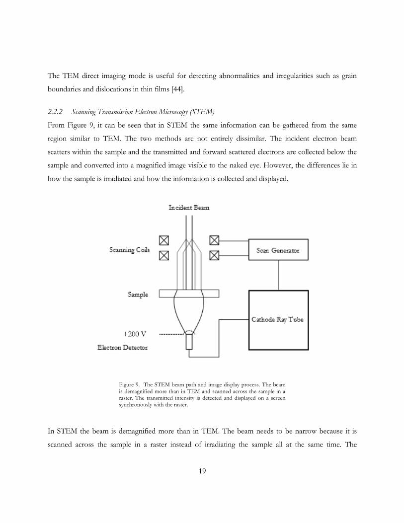
2.2.2 Scanning Transmission Electron Microscopy (STEM)
From Figure 9, it can be seen that in STEM the same information can be gathered from the same
region similar to TEM. The two methods are not entirely dissimilar. The incident electron beam
scatters within the sample and the transmitted and forward scattered electrons are collected below the
sample and converted into a magnified image visible to the naked eye. However, the differences lie in
how the sample is irradiated and how the information is collected and displayed.
Figure 9. The STEM beam path and image display process. The beam is demagnified more than in TEM and scanned across the sample in a raster. The transmitted intensity is detected and displayed on a screen synchronously with the raster.
In STEM the beam is demagnified more than in TEM. The beam needs to be narrow because it is
scanned across the sample in a raster instead of irradiating the sample all at the same time. The
+200 V
20
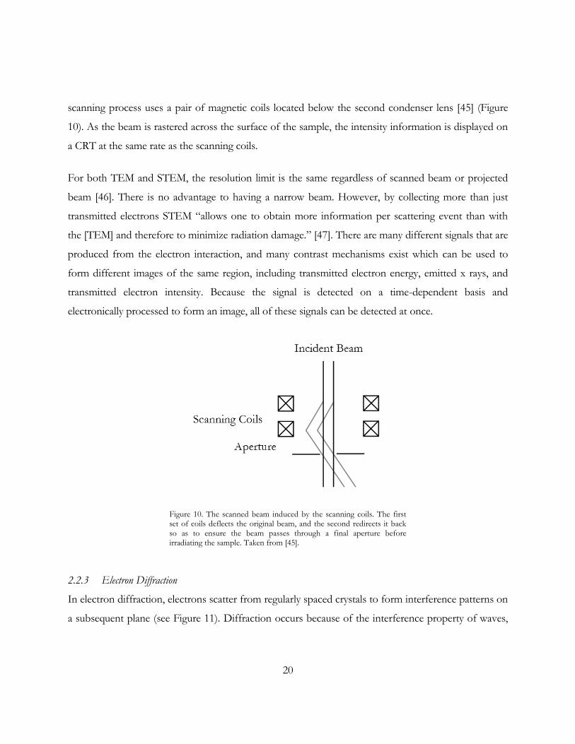
scanning process uses a pair of magnetic coils located below the second condenser lens [45] (Figure
10). As the beam is rastered across the surface of the sample, the intensity information is displayed on
a CRT at the same rate as the scanning coils.
For both TEM and STEM, the resolution limit is the same regardless of scanned beam or projected
beam [46]. There is no advantage to having a narrow beam. However, by collecting more than just
transmitted electrons STEM “allows one to obtain more information per scattering event than with
the [TEM] and therefore to minimize radiation damage.” [47]. There are many different signals that are
produced from the electron interaction, and many contrast mechanisms exist which can be used to
form different images of the same region, including transmitted electron energy, emitted x rays, and
transmitted electron intensity. Because the signal is detected on a time-dependent basis and
electronically processed to form an image, all of these signals can be detected at once.
Figure 10. The scanned beam induced by the scanning coils. The first set of coils deflects the original beam, and the second redirects it back so as to ensure the beam passes through a final aperture before irradiating the sample. Taken from [45].
2.2.3 Electron Diffraction
In electron diffraction, electrons scatter from regularly spaced crystals to form interference patterns on
a subsequent plane (see Figure 11). Diffraction occurs because of the interference property of waves,

21
both for electrons and photons. The principle of optical diffraction was first demonstrated by Thomas
Young when he passed coherent and divergent light through two circular apertures [48]. This
experiment has been replicated with slits instead and can be described quantitatively [42].
Figure 11. The diffracted electron beam path. The beam is incident on the sample and then projected. The diffracted image occurs on the focal plane where all the scattered electrons converge to produce rings or spots of greater intensity. Figure adapted from [25].
Let two rays and pass through separate slits and strike a screen at a distance L and height y
(Figure 12). Assuming that , the distance between scattering centers, the two rays and are
approximately parallel. It can be seen that
(2.15)
where
(2.16)
and m is an integer and λ is the wavelength of the incident particle. Substituting δ yields

22
(2.17)
It can be seen that under a small angle approximation
(2.18)
Figure 12. A diagram of Young’s double slit experiment. Coherent light was passed through two identical, narrow slits a distance d apart. The light was incident upon a screen a distance L from the slits. Adapted from Ref [49].
Substituting Equation 2.18 into Equation 2.17 yields
(2.19)
and solving for d yields
(2.20)

23
Thus the spacing d between scattering centers can be determined using the dimensions of a diffracted
image if the wavelength and separation distances are known.
Using a large number of slits results in a diffraction grating. This grating yields narrower intensity
peaks compared to two slits [49]. If the grating were etched in two dimensions with the rows
perpendicular, the resulting interference pattern would consist of a grid of dots. The arrangement of
slits in the diffraction grating determines the diffraction pattern.
Electron diffraction can occur because the incident beam of electrons behaves as a wave. The atoms in
a crystal lattice behave as scattering centers analogous to an optical diffraction grating, and thus
information regarding the crystal lattice can be determined by observing the diffraction patterns.
Specifically, electron diffraction can be used in thin film analysis because the diffraction patterns
correspond uniquely to each crystal lattice. The lattice spacing [43] and crystal orientation [25] can both
be determined using electron diffraction, both important features of thin films. For polycrystalline
films, the diffraction pattern will include information for the different grains superimposed together.
Inserting an aperture in the diffraction plane of the optical path affects the properties of the projected
image (Figure 13). If the direct image is allowed to pass through the aperture, the resulting image is the
bright field image. If a diffraction spot other than the direct beam is allowed to pass through, the
resulting image is the dark field image [43]. In thin film imaging, it is possible to differentiate specific
grains based on their dark field image, as long as the diffraction pattern can be analyzed to determine
grain orientation. The dark field picks a specific diffraction beam from specific reflecting planes in the
thin film grains and projects their image.
2.2.4 Scanning Electron Microscopy (SEM)
SEM is an imaging technique that scans an electron beam across the surface of a sample. The resulting
image is a topographic map of the surface of the sample. The beam is demagnified and focused down
to a convergent probe (Figure 14) and scanned across the sample as in STEM. Using thermionic
emission, the minimum diameter of the probe is on the order of tens of nanometers [45], much less
than in TEM.
24
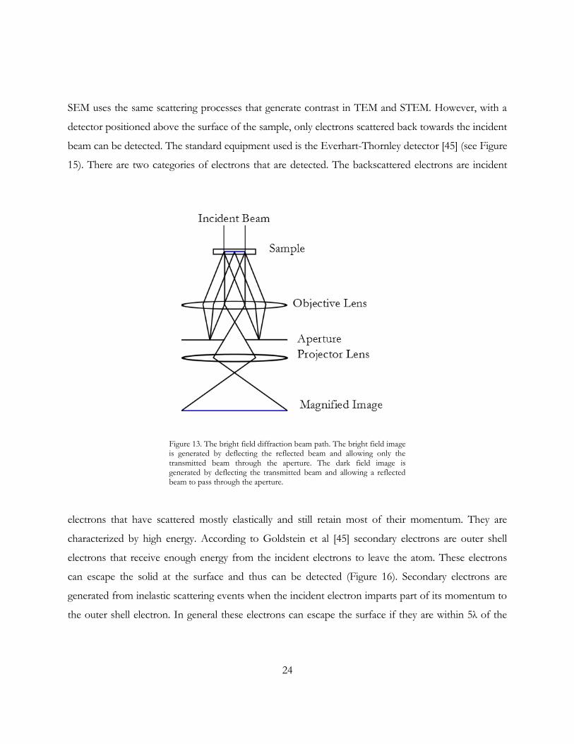
SEM uses the same scattering processes that generate contrast in TEM and STEM. However, with a
detector positioned above the surface of the sample, only electrons scattered back towards the incident
beam can be detected. The standard equipment used is the Everhart-Thornley detector [45] (see Figure
15). There are two categories of electrons that are detected. The backscattered electrons are incident
Figure 13. The bright field diffraction beam path. The bright field image is generated by deflecting the reflected beam and allowing only the transmitted beam through the aperture. The dark field image is generated by deflecting the transmitted beam and allowing a reflected beam to pass through the aperture.
electrons that have scattered mostly elastically and still retain most of their momentum. They are
characterized by high energy. According to Goldstein et al [45] secondary electrons are outer shell
electrons that receive enough energy from the incident electrons to leave the atom. These electrons
can escape the solid at the surface and thus can be detected (Figure 16). Secondary electrons are
generated from inelastic scattering events when the incident electron imparts part of its momentum to
the outer shell electron. In general these electrons can escape the surface if they are within 5λ of the

25
surface (Figure 16), where λ is the mean free path between scattering events [45]. The mean free path is
dependent on the density of the sample as well as the atomic number.
SEM uses backscattered and secondary electrons to form images in two modes. With the bias on the
Everhart-Thornley detector at 200 V, mostly secondary electrons are detected. The contrast is
dependent on atomic number and density as well since the secondary electrons are ejected along the
Figure 14. The SEM beam path and imaging process. The beam is highly demagnified and scanned across the sample in a raster. The scattered electrons are detected with an Everhart-Thornley detector and displayed in the same raster on a screen. Adapted from Ref [45].
trajectory of the incident electrons. Even though the beam diameter is only nanometers wide, the
interaction volume of incident electrons can be micrometers wide [45]. With secondary electrons,
surface features such as edges and non-perpendicular slopes are apparent [44]. At edges and slopes,
more backscattered and secondary electrons leave the sample due to the non-perpendicular surfaces
[45]. This also helps distinguish grain boundaries in thin films, since grain boundaries aren’t as
organized as the grains themselves.

26
In the second mode, a bias of -50V is applied to the detector. Backscattered electrons have higher
energy than secondary electrons [45], so only they will get detected. Contrast mechanisms are similar to
Figure 15. The Everhart-Thornley detector. The Faraday cage in front of the scintillator can be biased to filter out secondary electrons. The scintillator itself is held at around 12 kV. The detected electrons strike the scintillator and the light is amplified by a photomultiplier. Figure adapted from Ref [45].
those of secondary electron imaging, however, more information about the sample below the surface
is collected [45]. Also, the signal is lower with backscattered collection since the detector takes up a
small solid angle and the paths of the electrons do not bend as in secondary collection [45]. As can be
seen, SEM is a valuable imaging technique for thin films due to its surface sensitivity.
Figure 16. An incident electron traveling through a sample. The incident electrons may scatter loose specimen electrons and can exit the specimen as backscattered electrons. These secondary electrons can exit the sample if they are within 5λ of the surface (SEI and SEII) [36]. All three types of scattered electrons can be detected in SEM. Figure taken from [45].

27
Chapter 3
MICROSCOPE SYSTEMS
3.1 Vacuum System
The column has to be evacuated in order to run the electron microscope. Electrons interact with air
molecules, so scattering deflects electrons out of the beam alignment and reduces resolution. An
acceptable level of vacuum to reduce this is 10-5 Torr or better [49]. This ensures that most of the
electrons travel through the column without interacting with air molecules. In addition, the beam
source must be maintained at an even higher vacuum to reduce sparking due to its high voltage.
A high vacuum cannot be generated by one set of pumps alone. A pressure of down to 10-3 Torr can
be achieved by use of two rotary vane oil pumps (Figure 17A). These rotary pumps use the mechanical
action of an offset rotating vane to compress the air from the instrument and release it at atmospheric
pressure. This creates a rough vacuum, which serves as the outlet pressure for the high vacuum pumps
The diffusion pump is the high vacuum pump used in the JEOL CX-100. It has no moving parts and
uses oil as a medium. As is seen in Figure 17B, oil is heated and evaporated off. The oil particles travel
up the chimney and exit at high speed at the top. Here gas from the column can diffuse into the
stream, which is at lower pressure, being at high speed. The jet of gas creates a high-pressure
compression area at the bottom of the boiler. Here the pressurized gas is siphoned off and condensed
using water-cooled baffles. The condensed oil returns to the boiler, and the gas continues out the exit
towards the rotary pump.
The sample holding zone, gun, and camera are separately airlocked from the column. The gun is
separated by a small aperture to generate a separate, higher vacuum. The sample holder is airlocked for
changing out samples without venting the entire column. The camera is separate as well, for the same
reason; the film can be replaced without venting the column.

28
3.2 Beam Production
The electron source of the CX-100 is a tungsten filament. The filament is bent so the tip of the
filament is a sharp, narrow turn. The process by which electrons are generated is called thermionic
emission (Figure 18). The filament is heated by a high current. This increases the energy of the
Figure 17. Two vacuum pumps used in the JEOL CX-100. (A) Rotary Vane Pump, (B) Diffusion Pump. The rotary vane pump decompresses incoming air into a cavity and then pressurizes it above atmospheric pressure and forces it out through a one-way valve. The diffusion pump uses the kinetic energy of evaporated oil molecules to drive gas into a compression area, where the gas can leave through an outlet towards a backing pump. Adapted from Ref [50].
electrons in the filament. When the electrons are given enough thermal energy to exceed their work
function they leave the surface of the filament. This emission is described by Richard’s Law [43] as
(3.1)
where J is the emission current, T is the temperature of the sample (in K), Φ is the work function, k is
Boltzmann’s constant, and A is a proportionality constant characteristic for each material. A voltage
differential is produced between the filament—the cathode—and an anode, located below the
Wehnelt cap, in order to energize the electrons toward the specimen. For thermionic emission, the
energy spread ΔE is 3 eV [43]. The Wehnelt cap is biased to control the beam current and to create a
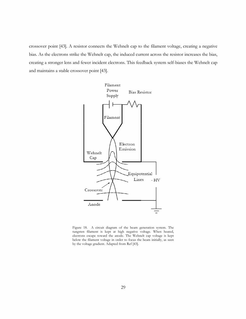
29
crossover point [43]. A resistor connects the Wehnelt cap to the filament voltage, creating a negative
bias. As the electrons strike the Wehnelt cap, the induced current across the resistor increases the bias,
creating a stronger lens and fewer incident electrons. This feedback system self-biases the Wehnelt cap
and maintains a stable crossover point [43].
Figure 18. A circuit diagram of the beam generation system. The tungsten filament is kept at high negative voltage. When heated, electrons escape toward the anode. The Wehnelt cap voltage is kept below the filament voltage in order to focus the beam initially, as seen by the voltage gradient. Adapted from Ref [43].

30
3.3 Image Processing
For SEM and backscatter, the electrons are detected using an Everhart-Thornley Detector [45]. This
signal goes through a preamplifier and an amplifier to increase the signal strength. Here the signal is
coupled with the scan signal that rastered the original electron beam and is sent to the CRT as a
stopping voltage. The CRT outputs a rastered signal whose current (and thus electron intensity) is
dependent on the voltage. A film cartridge is then exposed to the CRT output and the resulting
developed film becomes the final image. In TEM the projected image is captured using a camera with
film sensitive to electrons, similar to regular film cameras. In STEM the electron beam is detected
similar to SEM and scanned out on the CRT.

31
Chapter 4
REFURBISHMENT
4.1 Maintenance, Digital Image Conversion and Interface
The Houghton College microscope has an automated sequence for pumping down the column. The
microscope uses two rotary backing pumps; one for evacuating the microscope and one for a
desiccation chamber (Figure 19). Rotary pump one first evacuates the two diffusion pumps. Once they
are evacuated to 10-2 Torr the heating elements turn on and they begin depressurizing. If the pressure
inside is sufficiently low the column and gun will be opened to the diffusion pumps. Once the pressure
in the diffusion pumps is too high the valves to the column will close off and the diffusion pumps will
depressurize. Due to the presence of leaks in the equipment, the column is not sealed well enough to
hold a good vacuum while the diffusion pumps are depressurizing.
In order to accommodate this process, a manual pumping procedure was developed. Since the
microscope will be used primarily for the study of thin films, the second rotary pump was directly
attached to the column in order to evacuate it. In addition, a number of valves were manually powered
to control this evacuation. This allowed the user to pump down the column to a rough vacuum (10-2
Torr) before opening the diffusion pumps to the column. Once the diffusion pumps begin
depressurizing the column the user manually closes off the valve next to the rotary pump to prevent
the backstreaming of oil from the pump.
The valves used to control the depressurization of the microscope are driven by pneumatic pressure.
This allows the pressure to be controlled in various chambers in the microscope. The air compressor
used to generate the pneumatic pressure is air-cooled, and it turns off automatically if it overheats. This
compressor had been overheating regularly due to a ventilation issue inside the pump room, so an
extra cooling fan was installed to assist in heat transfer. This aided in reducing overheating, but the
problem has not been completely resolved to date.

32
Figure 19. A schematic diagram of the vacuum system for the JEOL CX-100. One rotary pump is the backing pump for the first diffusion pump. This pump in turn evacuates the column and the camera, and the second diffusion pump, which evacuates the gun at higher vacuum. The second rotary pump originally evacuated the desiccation chamber but was repurposed for evacuating the column. The in-line valves can be controlled manually.
Both the electromagnetic lenses and the diffusion pumps use water for a coolant, which is supplied by
a water-cooled chiller. The main pump for the chiller suffered a mechanical failure and was replaced.

33
4.2 Digital Image Conversion and Interface
Originally the imaging systems were designed for cartridge film, which is very difficult to acquire and
manipulate. Currently a program is being written using Labview to eliminate the need for film. This
program inputs the analog signals that scan and display an image onto a CRT screen and outputs a
two-dimensional array that represents that image. This array is exported to Microsoft Excel. The
elements of this array map to the electron intensities measured on specific locations on the specimen.
The CRT uses a voltage differential to focus electrons into a beam and accelerates them at a
fluorescent screen [42,50]. The electron beam is generated from the thermionic emission of a tungsten
filament (Figure 20). The beam current, and thus the beam intensity, is controlled by a negatively
biased grid near the filament. If the voltage differential between the filament and the grid is large
enough the emitted electrons will be deflected back toward the filament, reducing the beam current.
The filament is kept at ground, and the screen is kept at high voltage. The beam is focused using a
series of electrostatic lenses. These lenses are conducting cylinders, kept at successively higher voltage,
decreasing toward the screen. The potential gradient is highest in the gaps between the cylinders. This
gradient directs electrons toward the center of the beam axis, creating a convergent lens [42]. The
beam is deflected using two perpendicular sets of electromagnetic coils. These are placed around the
CRT after the beam is focused. The amount of deflection is proportional to the current through the
magnetic coils. The beam rastering mechanism is controlled by a sawtooth wave generator, which
cannot be located currently.
There are three signals that must be collected in order to output a digital image in SEM mode. The
first signal is the intensity signal. This determines how bright the electron beam is at any given location
on the scan and is directly proportional to the number of secondary electrons detected at that point
during the scan. This signal will be measured using the voltage differential between the filament and
the Wehnelt cap. The second and third signals are those which correspond to the horizontal and
vertical position of the electron beam, which was already discussed. The current of these coils was
measured indirectly using resistors in series. A voltage measurement was taken across a 0.5 Ω resistor
in series with each coil. This voltage is directly proportional to the current, which is directly

34
proportional to the position of the CRT beam. Next the voltages from the two resistors were scaled to
produce positive integers. These two integers were used as indices in a two-dimensional array, and the
scaled intensity voltage was used as the value for each element in the array. Data were collected and
deposited into an empty array at a rate of approximately 3000 Hz such that new elements were written
over the old values. The collection and overwriting process ran for several thousand iterations. This
large number was required to get a sampling that would assign a value to all but five elements in the
array. After the array was filled, the user was prompted to name and save the file in Excel. In the
future this file will be used to construct an image file.
Figure 20. The electron beam path through a cathode ray tube. Current across the filament induces thermionic emission. The filament is kept at high negative voltage, and the bias grid controls the beam current. The three apertures are kept at successively lower voltages and act as electrostatic convergent lenses. The electromagnetic coils on the sides of the CRT serve as deflector coils and cause the beam to scan across the screen in a raster. The screen is coated in a fluorescent material so the beam scan is visible to the naked eye.

35
Chapter 5
CONCLUSIONS AND FUTURE PLANS
The STEM is still in the process of refurbishment. There are several obstacles to overcome in order to
achieve focused beam operation. There are vacuum leaks that must be sealed. The air compressor
requires more ventilation to keep from overheating. As well, the compressed air system has several
small leaks that should be addressed in order to reduce the load on the compressor. The beam is not
focused or aligned correctly. After extensive testing, the condenser lens was found to be unresponsive
to adjustment, which will be attended to.
The Labview program is nearly complete. It takes analog data in from the CRT scan and writes the
intensity and position data into a two-dimensional array in a Microsoft Excel spreadsheet. Next, the
intensity signal must be written into the program so that the elements in the array can take in data
from the microscope. Currently the program writes a constant value for each element. After that, the
scan data should be written to an image file, with a save button to control which images are saved.
Currently the user is prompted to save every image generated. In addition, the resolution for the image
is not quickly adjustable. Creating a flexible resolution option would be useful.
As can be seen, the microscope is in need of some extensive maintenance. It still remains practical to
attend to the maintenance needs. The digital imaging and interface program is nearly finished, and
should complement the microscope once that is running. Houghton College’s JEOL CX-100 could
become a valuable tool in thin film research.

36
APPENDIX
A. Labview Diagram

37
R e f e r e n c e s
[1] A. Leeuwenhoek, Arcana naturae detecta (Delft: Delphis Batavorum and Henricum, Rome, 1695). [2]T. Young, A course of lectures on natural philosophy and the mechanical arts (William Savage,
London, 1807).
[3] L. de Broglie, Annales de Physique 10, 3 (1925).
[4] L. Davisson and C. Germer, The Physical Review 30, 6 (1927).
[5] H. Busch, Archiv für Elektrotechnik 18, 6 (1927).
[6] M. Knoll and E. Ruska, Zeitschrift für Technische Physik 12 (1931).
[7] M. Knoll and E. Ruska, Zeitschrift für Physik 78, 5-6 (1932).
[8] M. Knoll and E. Ruska, Annalen der Physik 404, 5-6 (1932).
[9] von Ardenne M. Z. Phys. 109, 553-572. (1938).
[10] V. Zworykin, Scientific American 167, (1942).
[11] Swiss Federal Institute of Technology, Zurich. http://www.microscopy.ethz.ch/ history.htm
[12] H. A. Macleod, Thin-Film Optical Filters, 3rd Ed. (Institute of Physics Publishing, Philadelphia, 2001).
[13] C. Sun, P. Jiang, B. Jiang, Applied Physics Letters 92, 061112 (2008).
[14] J. Xi, M. Schubert, J. Kim, E. Schubert, M. Chen, S. Lin, W. Liu, and J. Smart, Natural Photonics 1 (2007).
[15] N. D. S. Mohallem, M. M. Viana and R. A. Silva, New Trends and Developments in Automotive Industry (InTech, Rijeka, Croatia, 2011), pp. 347-64.
[16] R. Heck and R. Farrauto, Applied Catalysis A 221 (2001).
[17] K. E. Spear, Journal of the American Ceramics Society 72, 2 (1989).
[18] J. Kitamura, H. Mizuno, N. Kato and I. Aoki, Materials Transactions 47, 7 (2006).
[19] Y. He, R. Hattori, and J. Kanicki, IEEE Transactions on Electron Devices 48, 7 (2001).
[20] H. Q. Chiang, J. F. Wager, R. L. Hoffman, J. Jeong, and D. A. Keszler, Applied Physics Letters 86, 1 (2005).
[21] K. Nomura, H. Ohta, A. Takagi, T. Kamiya, M. Hirano, and H. Hosono, Nature 432, (2004).
[22] S. Ito, T. Murakami, P. Comte, P. Liska, C. Grätzel, M. Nazeeruddin, and M. Grätzel, Thin Solid Films 516 (2008).

38
[23] K. Chopra, P. Paulson, and V. Dutta, Progress in Photovoltaics: Research and
Applications 12 (2004).
[24] C. V. Thompson and R. Carel, Journal of the Mechanics and Physics of Solids, 44, 5 (1996).
[25] L. I. Maissel and R. Glang, Handbook of Thin Film Technology (McGraw-Hill Book Company, New York, 1970).
[26] K. R. Dixit, Philosophical Magazine and Journal of Science, 7th, 16, 109 (1933).
[27] L. H. Germer, Physical Review, 56 (1939).
[28] R. G. Picard and O. S. Duffendack, Journal of Applied Physics, 14, 6 (1943).
[29] H. Levinstein, Journal of Applied Physics, 20, 4 (1948).
[30] W. Brattain, Bell Labs logbook (December 24, 1947).
[31] J. Bardeen and W. H. Brattain, Physical Review 74 (1948).
[32] A. S. Norwick, Annual Review of Materials Science. 26,(1996).
[33] S. Karashima, Transactions of the Japan Institute of Metals 2 2 (1961).
[34] H. Mahl & W. Weitsch, Die Naturwissenschaften 47, 13, (1960).
[35] L. A. Bendersky and F. W. Gayle, Journal of Research of the National Institute of Standards and Technology, 106, 6 (2001).
[36] R. Dannenberg, E. A. Stach, J. R. Groza, and B. J. Dresser, Thin Solid Films, 370 (2000).
[37] F. Reniers, P. Kons, Pierre Delcambe, L. Binst, M. Jardinier-Offergeld and F. Bouillon. Microscopy, Microanalysis, Microstructures. 1. 189-197 (1990).
[38] J. Zhang, K. Xu, V. Ji, Applied Surface Science 187 (2002).
[39] S. Simões, R. Calinas, M. T. Vieira, M. F. Vieira, and P. J. Ferreira, Nanotechnology, 21 (2010).
[40] S. K. Bhagat and T. L. Alford. Journal of Applied Physics. 104. 103534 (2008).
[41] C. D. Dimitrakopoulos and Debra J. Mascaro, IBM Journal of Research and Development 45, 1 (2001).
[42]C. A. Bennett, Principles of Physical Optics (John Wiley & Sons, New York, 2008).
[43] D. B. Williams and C. B. Carter, Transmission Electron Microscopy (Springer, New York, 1996), Vol. I.
[44] M. Ohring, Materials Science of Thin Films: Deposition and Structure (Academic Press, San Diego, California, 2002).
[45] J. I. Goldstein, D. E. Newbury, P. Echlin, D. C. Joy, C. E. Lyman, E. Lifshin, L. Sawyer, and J. R. Michael, Scanning Electron Microscopy and X-Ray Microanalysis, (Kluwer Academic/Plenum Publishers, New York, 2003).
[46] P. J. Goodhew, J. Humphreys, and Richard Beanland, Electron Microscopy and Analysis (Taylor & Francis, New York, 2001) p. 222.
[47] J. Wall, J. Langmore, M. Isaacson, and V. Crewe, Proceedings of the National Academy of Science, USA 71 1 (1974).

39
[48] T. Young, A course of lectures on natural philosophy and the mechanical arts (William Savage, London,
1807).
[49] JEOL, Ltd; Instructions: JEM-100CX, p. 1-30.
[50] V. K. Zworykin, Proceedings of the IRE 21, 12 (1933).


![REFURBISHING A SCANNING TRANSMISSION ELECTRON … · 1.2.1 Wave-like Properties of Electrons In 1925, Louis de Broglie postulated that e lectrons have wave-like properties. [2] Previous](https://static.fdocuments.net/doc/165x107/5e7dfd8334528419aa7414ef/refurbishing-a-scanning-transmission-electron-121-wave-like-properties-of-electrons.jpg)