ReductionofElectricalDefectsinAtomicLayerDepositedHfO...
10
pubs.acs.org/cm Published on Web 06/28/2010 r 2010 American Chemical Society Chem. Mater. 2010, 22, 4175–4184 4175 DOI:10.1021/cm100620x Reduction of Electrical Defects in Atomic Layer Deposited HfO 2 Films by Al Doping Tae Joo Park, †,‡ Jeong Hwan Kim, †,‡ Jae Hyuck Jang, † Choong-Ki Lee, § Kwang Duk Na, † Sang Young Lee, † Hyung-Suk Jung, † Miyoung Kim, † Seungwu Han, † and Cheol Seong Hwang* ,† † Department of Materials Science and Engineering and Inter-university Semiconductor Research Center, Seoul National University, Seoul 151-744, Korea, and § School of Physics, Korea Institute for Advanced Study, Seoul 130-722, Korea. ‡ These authors equally contributed to this work Received February 28, 2010. Revised Manuscript Received June 9, 2010 The gate leakage current density (J g ) of ultrathin (∼3 nm) Al-doped HfO 2 (Al:HfO 2 ) films with an Al concentration of ∼11% was lower than that of the control HfO 2 film by 2 orders of magnitude at an equivalent oxide thickness of ∼1 nm. The permittivity of the Al:HfO 2 film was similar to that of the control HfO 2 film. Al doping of HfO 2 films reduced the concentration of the oxygen vacancies and carbon in the film, which act as electrical defects (traps). It also increased the band gap of the film, resulting in a reduced J g . Although the crystalline structure of a ∼ 12 nm-thick Al:HfO 2 film contained both tetragonal and monoclinic phases after high temperature annealing, the ∼3 nm thick Al:HfO 2 film showed a monoclinic structure, which is the same as the control HfO 2 film. Therefore, there was no modification of the crystalline structure of the Al:HfO 2 film in the ultrathin film case that would increase the permittivity. However, Si diffusion into the film and interfacial layer growth during annealing were suppressed significantly, which improved the thermal stability of the Al:HfO 2 films. Introduction Recently, post high-k gate dielectric materials with superior properties over that of the conventional high-k materials (HfO 2 , ZrO 2 , etc.) have been studied extensively to be used in advanced gate-stack structures in further- scaled metal-oxide-semiconductor field effect transistors (MOSFETs). 1,2 Most methods for improving the electri- cal properties of high-k films are based on the incorpora- tion of small concentrations of another material (doping) into conventional binary oxide high-k films. 3-20 In sev- eral experiments reporting the improved properties in doped high-k films, the increased permittivity was mainly attributed to the change in the crystalline structure of the film. 14-20 It was reported that the k values of HfO 2 and ZrO 2 are enhanced by doping with Y 2 O 3 , Al 2 O 3 , SiO 2 , etc. The crystalline structures of HfO 2 and ZrO 2 were modified by doping from monoclinic to tetragonal or cubic phases, which have a higher permittivity. 21-24 Therefore, a systematic understanding of the improved properties of doped high-k film from the other viewpoints *To whom correspondence should be addressed. E-mail: cheolsh@ snu.ac.kr. (1) Wilk, G. D.; Wallce, R. M.; Anthony, J. M. J. Appl. Phys. 2000, 87, 484. (2) Robertson, J. Rep. Prog. Phys. 2006, 69, 327. (3) Zhang, M. H.; Rhee, S. J.; Kang, C. Y.; Choi, C. H.; Akbar, M. S.; Krishnan, S. A.; Lee, T.; Ok, I. J.; Zhu, F.; Kim, H. S.; Lee, J. C. Appl. Phys. Lett. 2005, 87, 232901. (4) Yan, J.; Kuo, Y.; Lu, J. Electrochem. Solid-State Lett. 2007, 10, H199. (5) Cho, M.-H.; Moon, D. W.; Park, S. A.; Rho, Y. S.; Kim, Y. K.; Jeong, K.; Chang, C. H.; Gu, J. H.; Lee, J. H.; Choi, S. Y. Appl. Phys. Lett. 2004, 84, 678. (6) Lu, J.; Kuo, Y.; Tewg, J.-Y. J. Electrochem. Soc. 2006, 153, G410 __. (7) Tewg, J.-Y.; Kuo, Y.; Lu, J.; Schueler, B. W. J. Electrochem. Soc. 2004, 151, F59. (8) Kuo, Y.; Lu, J.; Yan, J.; Yuan, T.; Kim, H. C.; Peterson, J.; Gardner, M.; Chatterjee, S.; Luo, W. ECS Trans. 2005, 1, 447. (9) Senzaki, Y.; Park, S.; Chatham, H.; Bartholomew, L.; Nieveen, W. J. Vac. Sci. Technol., A 2004, 22, 1175. (10) Zhu, W. J.; Tamagawa, T.; Gibson, M.; Furukawa, T.; Ma, T. P. IEEE Electron Device Lett. 2002, 23, 649. (11) Rhee, S. J.; Kang, C. S.; Choi, C. H.; Kang, C. Y.; Krishnan, S. A.; Zhang, M. H.; Akbar, M. S.; Lee, J. C. IEEE Tech. Dig.-Int. Electron Devices Meet. 2004, 837. (12) Yang, Y.; Zhu, W.; Ma, T. P.; Stemmer, S. J. App. Phys. 2004, 95, 3772. (13) Yamamoto, Y.; Kita, K.; Kyuno, K.; Toriumi, A. Appl. Phys. Lett. 2006, 89, 032903. (14) Kita, K.; Kyuno, K.; Toriumi, A. Appl. Phys. Lett. 2005, 86, 102906. (15) Tomida, K.; Kita, K.; Toriumi, A. Appl. Phys. Lett. 2006, 89, 142902. (16) Boscke, T. S.; Govindarajan, S.; Kirch, P. D.; Hung, P. Y.; Krug, C.; Lee, B. H.; Heitmann, J.; Schroder, U.; Pant, G.; Gnade, B. E.; Krautschneider, W. H. Appl. Phys. Lett. 2007, 91, 072902. (17) Triyoso, D. H.; Hegde, R. I.; Schaeffer, J. K.; Roan, D.; Tobin, P. J.; Samavedam, S. B.; White, B. E., Jr.; Gregory, R.; Wang, X.-D. Appl. Phys. Lett. 2006, 88, 222901. (18) Hegde, R. I.; Triyoso, D. H.; Samavedam, S. B.; White, B. E., Jr. J. Appl. Phys. 2007, 101, 074113. (19) Triyoso, D. H.; Hegde, R. I.; Schaeffer, J. K.; Gregory, R.; Wang, X.-D.; Canonico, M.; Roan, D.; Hebert, E. A.; Kim, K.; Jiang, J.; Rai, R.; Kaushik, V.; Samavedam, S. B.; Rochat, N. Appl. Phys. Lett. 2006, 88, 222901. (20) Park, P. K.; Kang, S.-W. Appl. Phys. Lett. 2006, 89, 192905. (21) Zhao, X.; Vanderbilt, D. Phys. Rev. B. 2002, 65, 233106. (22) Lee, C.-K.; Cho, E.; Lee, H.-S.; Hwang., C. S.; Han, S. Phys. Rev. B. 2008, 78, 012102. (23) Fujimori, H.; Yashima, M.; Sasaki, S.; Kakihana, M.; Mori, T.; Tanaka, M.; Yoshimura, M. Chem. Phys. Lett. 2001, 346, 217. (24) Bernay, C.; Ringuede, A.; Colomban, P.; Lincot, D.; Cassir, M. J. Phys. Chem. Soilds. 2003, 64, 1761.
-
Upload
nguyenkhuong -
Category
Documents
-
view
239 -
download
0
Transcript of ReductionofElectricalDefectsinAtomicLayerDepositedHfO...
pubs.acs.org/cmPublished on Web 06/28/2010r 2010 American Chemical Society
Chem. Mater. 2010, 22, 4175–4184 4175DOI:10.1021/cm100620x
Reduction of Electrical Defects in Atomic LayerDepositedHfO2 Films by
Al Doping
Tae Joo Park,†,‡ Jeong Hwan Kim,†,‡ Jae Hyuck Jang,† Choong-Ki Lee,§ Kwang Duk Na,†
Sang Young Lee,† Hyung-Suk Jung,† Miyoung Kim,† Seungwu Han,† andCheol Seong Hwang*,†
†Department of Materials Science and Engineering and Inter-university Semiconductor Research Center,Seoul National University, Seoul 151-744, Korea, and §School of Physics, Korea Institute for Advanced
Study, Seoul 130-722, Korea. ‡These authors equally contributed to this work
Received February 28, 2010. Revised Manuscript Received June 9, 2010
The gate leakage current density (Jg) of ultrathin (∼3 nm) Al-doped HfO2 (Al:HfO2) films with an Alconcentration of ∼11% was lower than that of the control HfO2 film by 2 orders of magnitude at anequivalent oxide thickness of∼1nm.Thepermittivity of theAl:HfO2 filmwas similar to that of the controlHfO2 film. Al doping of HfO2 films reduced the concentration of the oxygen vacancies and carbon in thefilm, which act as electrical defects (traps). It also increased the band gap of the film, resulting in a reducedJg. Although the crystalline structure of a ∼ 12 nm-thick Al:HfO2 film contained both tetragonal andmonoclinic phases after high temperature annealing, the∼3 nm thick Al:HfO2 film showed a monoclinicstructure, which is the same as the control HfO2 film. Therefore, there was no modification of thecrystalline structure of the Al:HfO2 film in the ultrathin film case that would increase the permittivity.However, Si diffusion into the film and interfacial layer growth during annealing were suppressedsignificantly, which improved the thermal stability of the Al:HfO2 films.
Introduction
Recently, post high-k gate dielectric materials withsuperior properties over that of the conventional high-kmaterials (HfO2, ZrO2, etc.) have been studied extensivelyto be used in advanced gate-stack structures in further-scaled metal-oxide-semiconductor field effect transistors(MOSFETs).1,2 Most methods for improving the electri-cal properties of high-k films are based on the incorpora-tion of small concentrations of another material (doping)
into conventional binary oxide high-k films.3-20 In sev-eral experiments reporting the improved properties indoped high-k films, the increased permittivity was mainlyattributed to the change in the crystalline structure of thefilm.14-20 It was reported that the k values of HfO2 andZrO2 are enhanced by doping with Y2O3, Al2O3, SiO2,etc. The crystalline structures of HfO2 and ZrO2 weremodified by doping from monoclinic to tetragonal orcubic phases, which have a higher permittivity.21-24
Therefore, a systematic understanding of the improvedproperties of doped high-k film from the other viewpoints
*To whom correspondence should be addressed. E-mail: [email protected].(1) Wilk, G. D.;Wallce, R.M.; Anthony, J.M. J. Appl. Phys. 2000, 87,
484.(2) Robertson, J. Rep. Prog. Phys. 2006, 69, 327.(3) Zhang,M. H.; Rhee, S. J.; Kang, C. Y.; Choi, C. H.; Akbar,M. S.;
Krishnan, S. A.; Lee, T.; Ok, I. J.; Zhu, F.; Kim, H. S.; Lee, J. C.Appl. Phys. Lett. 2005, 87, 232901.
(4) Yan, J.; Kuo, Y.; Lu, J. Electrochem. Solid-State Lett. 2007, 10,H199.
(5) Cho, M.-H.; Moon, D. W.; Park, S. A.; Rho, Y. S.; Kim, Y. K.;Jeong, K.; Chang, C. H.; Gu, J. H.; Lee, J. H.; Choi, S. Y. Appl.Phys. Lett. 2004, 84, 678.
(6) Lu, J.; Kuo, Y.; Tewg, J.-Y. J. Electrochem. Soc. 2006, 153,G410 __.
(7) Tewg, J.-Y.; Kuo, Y.; Lu, J.; Schueler, B. W. J. Electrochem. Soc.2004, 151, F59.
(8) Kuo, Y.; Lu, J.; Yan, J.; Yuan, T.; Kim, H. C.; Peterson, J.;Gardner, M.; Chatterjee, S.; Luo, W. ECS Trans. 2005, 1, 447.
(9) Senzaki, Y.; Park, S.; Chatham,H.; Bartholomew, L.; Nieveen,W.J. Vac. Sci. Technol., A 2004, 22, 1175.
(10) Zhu, W. J.; Tamagawa, T.; Gibson, M.; Furukawa, T.; Ma, T. P.IEEE Electron Device Lett. 2002, 23, 649.
(11) Rhee, S. J.; Kang, C. S.; Choi, C. H.; Kang, C. Y.; Krishnan, S. A.;Zhang, M. H.; Akbar, M. S.; Lee, J. C. IEEE Tech. Dig.-Int.Electron Devices Meet. 2004, 837.
(12) Yang, Y.; Zhu, W.; Ma, T. P.; Stemmer, S. J. App. Phys. 2004, 95,3772.
(13) Yamamoto, Y.; Kita, K.; Kyuno,K.; Toriumi, A.Appl. Phys. Lett.2006, 89, 032903.
(14) Kita, K.; Kyuno, K.; Toriumi, A. Appl. Phys. Lett. 2005, 86,102906.
(15) Tomida, K.; Kita, K.; Toriumi, A. Appl. Phys. Lett. 2006, 89,142902.
(16) Boscke, T. S.; Govindarajan, S.; Kirch, P. D.; Hung, P. Y.; Krug,C.; Lee, B. H.; Heitmann, J.; Schroder, U.; Pant, G.; Gnade, B. E.;Krautschneider, W. H. Appl. Phys. Lett. 2007, 91, 072902.
(17) Triyoso, D. H.; Hegde, R. I.; Schaeffer, J. K.; Roan, D.; Tobin,P. J.; Samavedam, S. B.; White, B. E., Jr.; Gregory, R.; Wang,X.-D. Appl. Phys. Lett. 2006, 88, 222901.
(18) Hegde, R. I.; Triyoso, D. H.; Samavedam, S. B.; White, B. E., Jr.J. Appl. Phys. 2007, 101, 074113.
(19) Triyoso, D. H.; Hegde, R. I.; Schaeffer, J. K.; Gregory, R.; Wang,X.-D.; Canonico, M.; Roan, D.; Hebert, E. A.; Kim, K.; Jiang, J.;Rai, R.; Kaushik, V.; Samavedam, S. B.; Rochat, N. Appl. Phys.Lett. 2006, 88, 222901.
(20) Park, P. K.; Kang, S.-W. Appl. Phys. Lett. 2006, 89, 192905.(21) Zhao, X.; Vanderbilt, D. Phys. Rev. B. 2002, 65, 233106.(22) Lee, C.-K.; Cho, E.; Lee, H.-S.; Hwang., C. S.; Han, S. Phys. Rev.
B. 2008, 78, 012102.(23) Fujimori, H.; Yashima, M.; Sasaki, S.; Kakihana, M.; Mori, T.;
Tanaka, M.; Yoshimura, M. Chem. Phys. Lett. 2001, 346, 217.(24) Bernay, C.; Ringuede, A.; Colomban, P.; Lincot, D.; Cassir, M. J.
Phys. Chem. Soilds. 2003, 64, 1761.
4176 Chem. Mater., Vol. 22, No. 14, 2010 Park et al.
is insufficient. In addition, the improved properties ofdoped high-k films with an amorphous structure aredifficult to explain using the crystalline structure modelat present. In addition, the crystallization of high-k filmsis affected not only by doping but also by other factors,such as the film thickness, stress from the substrate, andthe diffusion of substrate elements. Therefore, it is im-portant to examine the parameters that affect the crystal-line structure of doped high-k films.In this study,Al-dopedHfO2 (Al:HfO2) filmswith various
Al concentrations were grown by atomic layer deposition(ALD). The electrical and chemical properties as well as thethermal stability of the films were evaluated. The origins ofthe improved electrical properties were examined systemi-cally by analyzing the following: (i) the chemical structure,(ii) the state of electrical defects, (iii) the electronic structures,(iv) the crystalline structures, and (v) the interfacial reactionsof the Al:HfO2 films with the Si substrate.
Experimental Section
Sample Preparations. The control HfO2 and Al-doped HfO2
thin films were grown to a thickness of∼3 to∼20 nm at 280 �C on
4 in. diameter p-type (100) Si substrates by thermal ALD using
Hf[N(CH3)(C2H5)]4 (TEMAH) and Al(CH3)3 (TMA) as the Hf
and Al precursors, respectively. O3 at a concentration of 165 g/m3
was used as the oxygen source. An Al-O layer was inserted
discretely into the film by substituting one Hf-O cycle with one
Al-Ocycle among a total of 30ALDcycles to allow the incorpora-
tionofAl ions into the films.Accordingly, to grow the controlHfO2
andAl-dopedHfO2 films with different Al concentrations, we con-
trolled the number of ALD cycles to 30 (TEMAH) for the control
HfO2 film, 15(TEMAH)/1(TMA)/14 (TEMAH) for the HAO1
film, 10/1/9/1/9 for theHAO2 film, and7/1/7/1/7/1/6 for theHAO3
film. PDAwas performed by rapid thermal annealing at 850 �C for
30 s under a N2 atmosphere. Sputtered Pt as the top electrode was
deposited through a shadow mask to fabricate the metal-insulator-semiconductor capacitors. Forming gas annealing was
performed at 400 �C for 10 min in a 95% N2/5% H2 atmosphere
after the formation of a Pt top electrode.
Analyses and Measurements. The depth profiles of the chemi-
cal compositions in the control HfO2 and Al:HfO2 films were
examined by time-of-flight SIMS. The quantitative chemical com-
positionsof the controlHfO2andAl:HfO2 filmswereestimatedbya
STEM-EDS and RBS under an oxygen resonance condition (Heþ
ion acceleration energy of 3.04 MeV) to observe the oxygen
concentration precisely. The chemical binding status and valence
band spectra of the filmwas examinedbyhigh resolutionXPSusing
Al KR as the X-ray source. The binding energies of the XP spectra
were calibrated using the Si-Si binding energy in the Si 2p XP
spectra from the Si substrate (99.0 eV). The thicknesses and micro-
structures of the films were observed by HRTEM equipped with a
field emission electron gun. The physical thicknesses of the films
were also measured by ellipsometry. The typical capacitance-voltage (C-V) and Jg-Vmeasurements were performed using an
HP 4194 impedance analyzer and HP 4140B picoammeter/dc
voltage source, respectively. The EOT was calculated from the
accumulation capacitance usign the two frequency method 25
considering the quantum mechanical effect. The frequencies of the
C-Vmeasurement were 500 kHz and 1 MHz. The VFB value was
determined from the calculated flatband capacitance values using
the measured C-V curve. The size of the top electrodes was
measured carefully by optical microscopy. For an analysis of the
Jg mechanism, the Jg-V characteristics were collected at several
different temperatures (from 75 to 135 �C) using an HP 4145B
semiconductor parameter analyzer.
Theoretical Calculations. Theoretical investigations were per-
formed based on density functional theory. The optimized
atomic and electronic structure were examined using a Vienna
ab initio simulation package.26,27 The generalized gradient
approximation was used for exchange-correlation potential,
and projector-augmented wave method was employed to de-
scribe the electron-ion interaction. The k-points were sampled
with 2� 2� 2 uniform grids. Plane waves up to an energy cutoff
of 500 eV were used to expand the electronic wave functions.
The forces on the atoms and stress on the cell were reduced to
below 0.02 eV/A and 1 kb, respectively.
Results and Discussion
Chemical and Physical Structures of Al:HfO2 Thin
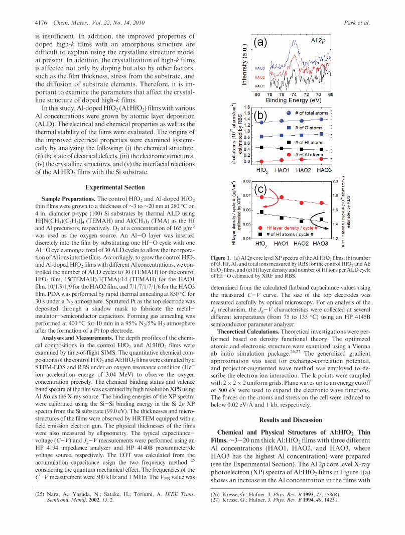
Films.∼3-20 nm thick Al:HfO2 films with three differentAl concentrations (HAO1, HAO2, and HAO3, whereHAO3 has the highest Al concentration) were prepared(see the Experimental Section). The Al 2p core level X-rayphotoelectron (XP) spectra of Al:HfO2 films inFigure 1(a)shows an increase in the Al concentration in the films with
Figure 1. (a) Al 2p core levelXP spectra of theAl:HfO2 films, (b) numberofO,Hf,Al, and total ionsmeasuredbyRBS for the controlHfO2 andAl:HfO2 films, and (c)Hf layer density and number ofHf ions perALDcycleof Hf-O estimated by XRF and RBS.
(25) Nara, A.; Yasuda, N.; Satake, H.; Toriumi, A. IEEE Trans.Semicond. Manuf. 2002, 15, 2.
(26) Kresse, G.; Hafner, J. Phys. Rev. B 1993, 47, 558(R).(27) Kresse, G.; Hafner, J. Phys. Rev. B 1994, 49, 14251.
Article Chem. Mater., Vol. 22, No. 14, 2010 4177
increasingALDcycle number ofAl-O.The thickness of theAl:HfO2 films used for XP spectroscopy (XPS) analysis inFigure 1a was controlled to ∼20 nm by repeating the unit30ALDcycles to remove the interface effects at the interfacewith the Si substrate on Al incorporation into the film.Figure 1b shows the atomic number density (number ofatoms per volume) of each element in the control HfO2 andAl:HfO2 films, which was estimated by Rutherford back-scattering spectroscopy (RBS) under the oxygen resonancecondition. The film thickness was the same (∼ 20 nm) asthose used forXPS analysis in Figure 1a. The atomic densityof Hf and Al respectively decreased and increased withincreasing number of ALD cycles of Al-O. The growthrates of the ALDHfO2 and Al2O3 films were similar,∼0.09nm/cycle. This means that the combined volume of HfO2
andAl2O3molecules depositedperALDcycle is similar. ThebulkatomicdensityofHfO2andAl2O3 filmswas∼0.046and∼0.039 mol/cm3, respectively. Therefore, the amount of HfandO ions (forHfO2) deposited per anALD cycle ofHf-Ois proportional to the bulk atomic density of HfO2,∼ 0.046and∼0.092mol/cm-3 (0.046mol/cm3� 2), respectively, be-cause the number of Hf and O ions per a single HfO2 mole-cule is one and two, respectively. In the same respect, theamount of Al andO ions (for Al2O3) deposited per an ALDcycle ofAl-Ois alsoproportional to thebulk atomicdensityof Al2O3, ∼0.078 (≈ 0.039 � 2) and ∼0.117 mol/cm3
(≈ 0.039 � 3), respectively, because the number of Al andO ions per a single Al2O3 molecule is two and three,respectively. As a result, when oneHf-Ocycle is substitutedwith one Al-O cycle, the number of O ions and anions(HfþAl) increased compared to that of the control HfO2
film, because Al2O3 generated by one Al-O cycle has moreO ions than HfO2 generated by one Hf-O cycle (3 and 2 Oions for Al2O3 andHfO2, respectively). This is supported bythe increased number of O and total ions with increasingnumber of ALD cycles of Al-O, as shown in Figure 1b.TheAl concentrations in theAl:HfO2 filmswere examined
by XPS, RBS and scanning transmission electron micro-scopy - energy dispersiveX-ray spectroscopy (STEM-EDS),as summarized in Table 1. The values for the “ideal”, whichwere calculated using the bulk atomic density of HfO2 andAl2O3, as mentioned above, were also included. The “ideal”Al concentration in the film corresponds to the case wherethe incorporation rate of each layer(Al-O and Hf-O) intothe film was not influenced by the presence of other layer.Figure 1c shows the Hf layer density and number of Hf ionsdeposited per ALD cycle of Hf-O estimated by X-rayflorescence (XRF) and RBS, respectively. Both XRF andRBS results showed that the growth of the HfO2 layer wasretarded further with increasing number of ALD cycles of
Al-O. Therefore, the measured Al concentration in theAl:HfO2 films was slightly larger than the “ideal” values,as shown in Table 1.Although the film thickness used for STEM-EDS was
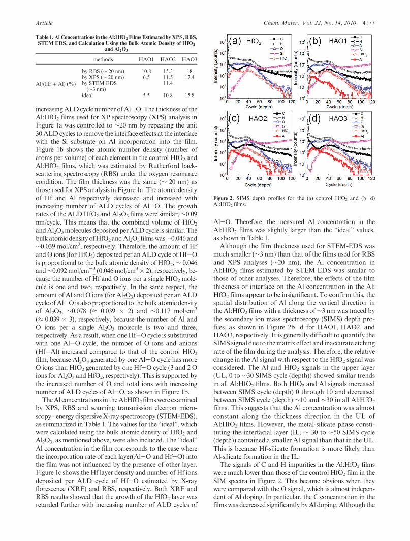
much smaller (∼3 nm) than that of the films used for RBSand XPS analyses (∼20 nm), the Al concentration inAl:HfO2 films estimated by STEM-EDS was similar tothose of other analyses. Therefore, the effects of the filmthickness or interface on the Al concentration in the Al:HfO2 films appear to be insignificant. To confirm this, thespatial distribution of Al along the vertical direction inthe Al:HfO2 films with a thickness of∼3 nmwas traced bythe secondary ion mass spectroscopy (SIMS) depth pro-files, as shown in Figure 2b-d for HAO1, HAO2, andHAO3, respectively. It is generally difficult to quantify theSIMS signal due to thematrix effect and inaccurate etchingrate of the film during the analysis. Therefore, the relativechange in the Al signal with respect to the HfO2 signal wasconsidered. The Al and HfO2 signals in the upper layer(UL, 0 to ∼30 SIMS cycle (depth)) showed similar trendsin all Al:HfO2 films. Both HfO2 and Al signals increasedbetween SIMS cycle (depth) 0 through 10 and decreasedbetween SIMS cycle (depth) ∼10 and ∼30 in all Al:HfO2
films. This suggests that the Al concentration was almostconstant along the thickness direction in the UL ofAl:HfO2 films. However, the metal-silicate phase consti-tuting the interfacial layer (IL, ∼ 30 to ∼50 SIMS cycle(depth)) contained a smaller Al signal than that in the UL.This is because Hf-silicate formation is more likely thanAl-silicate formation in the IL.The signals of C and H impurities in the Al:HfO2 films
were much lower than those of the control HfO2 film in theSIM spectra in Figure 2. This became obvious when theywere compared with the O signal, which is almost indepen-dent of Al doping. In particular, the C concentration in thefilmswas decreased significantly byAl doping.Although the
Table 1. Al Concentrations in the Al:HfO2 Films Estimated byXPS, RBS,
STEM EDS, and Calculation Using the Bulk Atomic Density of HfO2
and Al2O3
methods HAO1 HAO2 HAO3
Al/(Hf þ Al) (%)
by RBS (∼ 20 nm) 10.8 15.3 18by XPS (∼ 20 nm) 6.5 11.5 17.4by STEM EDS(∼3 nm)
11.4
ideal 5.5 10.8 15.8
Figure 2. SIMS depth profiles for the (a) control HfO2 and (b-d)Al:HfO2 films.
4178 Chem. Mater., Vol. 22, No. 14, 2010 Park et al.
origin of the reduced impurities in the Al:HfO2 films isunclear,28 this appears to have a close relationship with theconcentration of oxygen vacancies (VO) in the Al:HfO2
films. When a molecule of TEMAH and TMA precursorcontains twelve and three C atoms, respectively, it is alsopossible that the reduced supply of C atoms from theprecursor ligands decreased the C concentration in theAl:HfO2 films. However, the difference in C concentrationbetween the control HfO2 and the Al:HfO2 films is muchlarger than what is expected based on the difference in thesupplied amount of C atoms from the precursor ligands.Although the difference in the supplied amount of C atomsbetween the controlHfO2and theAl:HfO2 films [TEMAH/TMA ratios of 29/1(HAO1), 28/2 (HAO2), and 27/3-(HAO3)] is ∼2.5-7.5%, SIMS results showed that thedifference in C concentration between the control HfO2
and the Al:HfO2 films is much larger.The VO concentration in the Al:HfO2 films was estimated
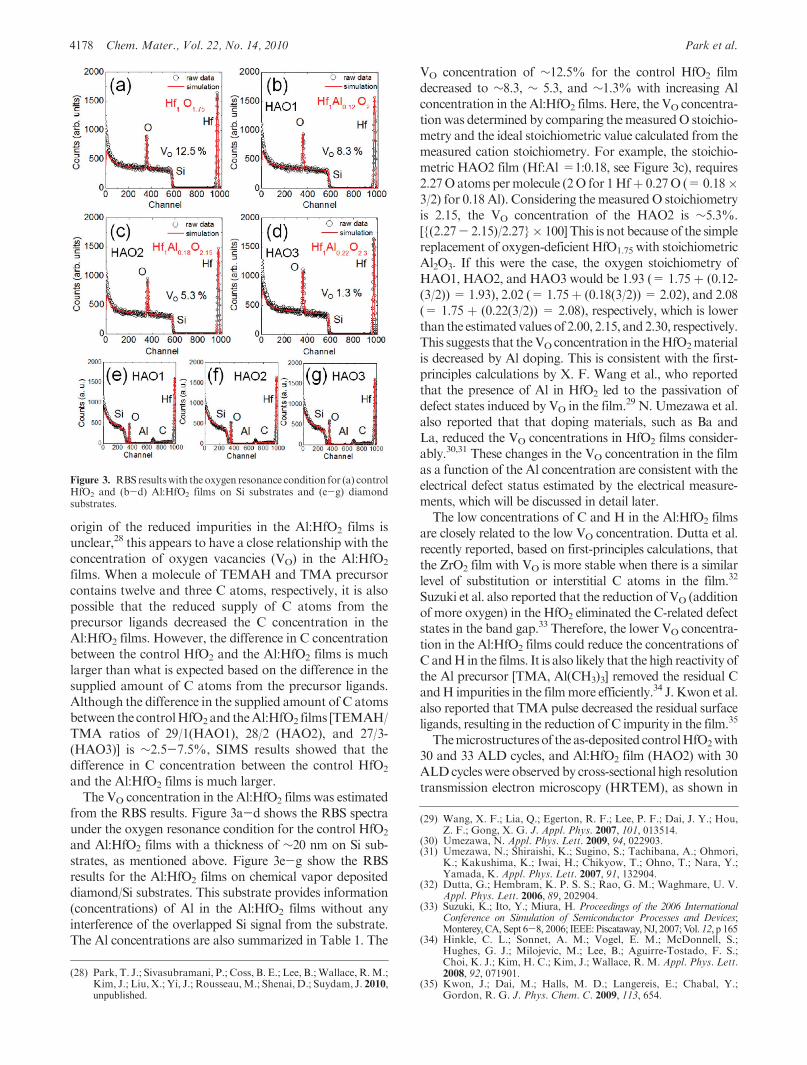
from the RBS results. Figure 3a-d shows the RBS spectraunder the oxygen resonance condition for the control HfO2
and Al:HfO2 films with a thickness of ∼20 nm on Si sub-strates, as mentioned above. Figure 3e-g show the RBSresults for the Al:HfO2 films on chemical vapor depositeddiamond/Si substrates. This substrate provides information(concentrations) of Al in the Al:HfO2 films without anyinterference of the overlapped Si signal from the substrate.The Al concentrations are also summarized in Table 1. The
VO concentration of ∼12.5% for the control HfO2 filmdecreased to ∼8.3, ∼ 5.3, and ∼1.3% with increasing Alconcentration in the Al:HfO2 films. Here, the VO concentra-tion was determined by comparing themeasuredO stoichio-metry and the ideal stoichiometric value calculated from themeasured cation stoichiometry. For example, the stoichio-metric HAO2 film (Hf:Al =1:0.18, see Figure 3c), requires2.27O atoms permolecule (2O for 1Hfþ 0.27O (=0.18�3/2) for 0.18Al). Considering themeasuredO stoichiometryis 2.15, the VO concentration of the HAO2 is ∼5.3%.[{(2.27- 2.15)/2.27}� 100] This is not because of the simplereplacement of oxygen-deficient HfO1.75 with stoichiometricAl2O3. If this were the case, the oxygen stoichiometry ofHAO1, HAO2, and HAO3 would be 1.93 (= 1.75þ (0.12-(3/2)) = 1.93), 2.02 (= 1.75þ (0.18(3/2)) = 2.02), and 2.08(= 1.75 þ (0.22(3/2)) = 2.08), respectively, which is lowerthan the estimatedvalues of 2.00, 2.15, and2.30, respectively.This suggests that theVO concentration in theHfO2materialis decreased by Al doping. This is consistent with the first-principles calculations by X. F. Wang et al., who reportedthat the presence of Al in HfO2 led to the passivation ofdefect states induced by VO in the film.29 N. Umezawa et al.also reported that that doping materials, such as Ba andLa, reduced the VO concentrations in HfO2 films consider-ably.30,31 These changes in the VO concentration in the filmas a function of the Al concentration are consistent with theelectrical defect status estimated by the electrical measure-ments, which will be discussed in detail later.The low concentrations of C and H in the Al:HfO2 films
are closely related to the low VO concentration. Dutta et al.recently reported, based on first-principles calculations, thatthe ZrO2 film with VO is more stable when there is a similarlevel of substitution or interstitial C atoms in the film.32
Suzuki et al. also reported that the reduction of VO (additionof more oxygen) in the HfO2 eliminated the C-related defectstates in the band gap.33 Therefore, the lower VO concentra-tion in the Al:HfO2 films could reduce the concentrations ofC andH in the films. It is also likely that the high reactivity ofthe Al precursor [TMA, Al(CH3)3] removed the residual CandH impurities in the filmmore efficiently.34 J. Kwon et al.also reported that TMA pulse decreased the residual surfaceligands, resulting in the reduction of C impurity in the film.35
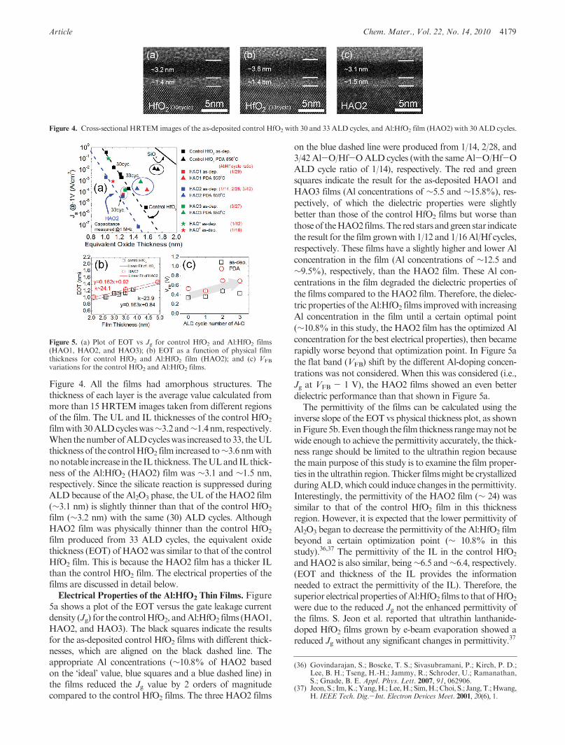
Themicrostructuresof the as-deposited controlHfO2with30 and 33 ALD cycles, and Al:HfO2 film (HAO2) with 30ALDcycleswere observed by cross-sectional high resolutiontransmission electron microscopy (HRTEM), as shown in
Figure 3. RBSresultswith the oxygen resonance condition for (a) controlHfO2 and (b-d) Al:HfO2 films on Si substrates and (e-g) diamondsubstrates.
(28) Park, T. J.; Sivasubramani, P.; Coss, B. E.; Lee, B.;Wallace, R.M.;Kim, J.; Liu, X.; Yi, J.; Rousseau,M.; Shenai, D.; Suydam, J. 2010,unpublished.
(29) Wang, X. F.; Lia, Q.; Egerton, R. F.; Lee, P. F.; Dai, J. Y.; Hou,Z. F.; Gong, X. G. J. Appl. Phys. 2007, 101, 013514.
(30) Umezawa, N. Appl. Phys. Lett. 2009, 94, 022903.(31) Umezawa, N.; Shiraishi, K.; Sugino, S.; Tachibana, A.; Ohmori,
K.; Kakushima, K.; Iwai, H.; Chikyow, T.; Ohno, T.; Nara, Y.;Yamada, K. Appl. Phys. Lett. 2007, 91, 132904.
(32) Dutta, G.; Hembram, K. P. S. S.; Rao, G. M.; Waghmare, U. V.Appl. Phys. Lett. 2006, 89, 202904.
(33) Suzuki, K.; Ito, Y.; Miura, H. Proceedings of the 2006 InternationalConference on Simulation of Semiconductor Processes and Devices;Monterey, CA, Sept 6-8, 2006; IEEE: Piscataway,NJ, 2007;Vol. 12, p 165
(34) Hinkle, C. L.; Sonnet, A. M.; Vogel, E. M.; McDonnell, S.;Hughes, G. J.; Milojevic, M.; Lee, B.; Aguirre-Tostado, F. S.;Choi, K. J.; Kim, H. C.; Kim, J.; Wallace, R. M. Appl. Phys. Lett.2008, 92, 071901.
(35) Kwon, J.; Dai, M.; Halls, M. D.; Langereis, E.; Chabal, Y.;Gordon, R. G. J. Phys. Chem. C. 2009, 113, 654.
Article Chem. Mater., Vol. 22, No. 14, 2010 4179
Figure 4. All the films had amorphous structures. Thethickness of each layer is the average value calculated frommore than 15 HRTEM images taken from different regionsof the film. The UL and IL thicknesses of the control HfO2
filmwith 30ALDcycleswas∼3.2 and∼1.4nm, respectively.When thenumberofALDcycleswas increased to33, theULthickness of the controlHfO2 film increased to∼3.6 nmwithnonotable increase in the IL thickness.TheULand IL thick-ness of the Al:HfO2 (HAO2) film was ∼3.1 and ∼1.5 nm,respectively. Since the silicate reaction is suppressed duringALD because of the Al2O3 phase, the UL of the HAO2 film(∼3.1 nm) is slightly thinner than that of the control HfO2
film (∼3.2 nm) with the same (30) ALD cycles. AlthoughHAO2 film was physically thinner than the control HfO2
film produced from 33 ALD cycles, the equivalent oxidethickness (EOT) of HAO2was similar to that of the controlHfO2 film. This is because the HAO2 film has a thicker ILthan the control HfO2 film. The electrical properties of thefilms are discussed in detail below.Electrical Properties of the Al:HfO2 Thin Films. Figure
5a shows a plot of the EOT versus the gate leakage currentdensity (Jg) for the controlHfO2, andAl:HfO2 films (HAO1,HAO2, and HAO3). The black squares indicate the resultsfor the as-deposited control HfO2 films with different thick-nesses, which are aligned on the black dashed line. Theappropriate Al concentrations (∼10.8% of HAO2 basedon the ‘ideal’ value, blue squares and a blue dashed line) inthe films reduced the Jg value by 2 orders of magnitudecompared to the control HfO2 films. The three HAO2 films
on the blue dashed line were produced from 1/14, 2/28, and3/42 Al-O/Hf-OALD cycles (with the sameAl-O/Hf-OALD cycle ratio of 1/14), respectively. The red and greensquares indicate the result for the as-deposited HAO1 and
HAO3 films (Al concentrations of ∼5.5 and ∼15.8%), res-
pectively, of which the dielectric properties were slightly
better than those of the control HfO2 films but worse than
thoseof theHAO2films.The red stars andgreen star indicate
the result for the film grownwith 1/12 and 1/16Al/Hf cycles,
respectively. These films have a slightly higher and lower Al
concentration in the film (Al concentrations of ∼12.5 and
∼9.5%), respectively, than the HAO2 film. These Al con-
centrations in the film degraded the dielectric properties of
the films compared to the HAO2 film. Therefore, the dielec-
tric properties of theAl:HfO2 films improvedwith increasing
Al concentration in the film until a certain optimal point
(∼10.8% in this study, the HAO2 film has the optimized Al
concentration for the best electrical properties), then became
rapidly worse beyond that optimization point. In Figure 5a
the flat band (VFB) shift by the different Al-doping concen-
trations was not considered. When this was considered (i.e.,
Jg at VFB - 1 V), the HAO2 films showed an even better
dielectric performance than that shown in Figure 5a.The permittivity of the films can be calculated using the
inverse slope of the EOT vs physical thickness plot, as showninFigure5b.Even though the filmthickness rangemaynotbewide enough to achieve the permittivity accurately, the thick-ness range should be limited to the ultrathin region becausethe main purpose of this study is to examine the film proper-ties in the ultrathin region. Thicker filmsmight be crystallizedduringALD, which could induce changes in the permittivity.Interestingly, the permittivity of the HAO2 film (∼ 24) wassimilar to that of the control HfO2 film in this thicknessregion. However, it is expected that the lower permittivity ofAl2O3 began to decrease the permittivity of the Al:HfO2 filmbeyond a certain optimization point (∼ 10.8% in thisstudy).36,37 The permittivity of the IL in the control HfO2
andHAO2 is also similar, being∼6.5 and∼6.4, respectively.(EOT and thickness of the IL provides the informationneeded to extract the permittivity of the IL). Therefore, thesuperior electrical properties ofAl:HfO2 films to that ofHfO2
were due to the reduced Jg not the enhanced permittivity ofthe films. S. Jeon et al. reported that ultrathin lanthanide-doped HfO2 films grown by e-beam evaporation showed areduced Jg without any significant changes in permittivity.37
Figure 4. Cross-sectional HRTEM images of the as-deposited control HfO2 with 30 and 33 ALD cycles, and Al:HfO2 film (HAO2) with 30 ALD cycles.
Figure 5. (a) Plot of EOT vs Jg for control HfO2 and Al:HfO2 films(HAO1, HAO2, and HAO3); (b) EOT as a function of physical filmthickness for control HfO2 and Al:HfO2 film (HAO2); and (c) VFB
variations for the control HfO2 and Al:HfO2 films.
(36) Govindarajan, S.; Boscke, T. S.; Sivasubramani, P.; Kirch, P. D.;Lee, B. H.; Tseng, H.-H.; Jammy, R.; Schroder, U.; Ramanathan,S.; Gnade, B. E. Appl. Phys. Lett. 2007, 91, 062906.
(37) Jeon, S.; Im,K.;Yang,H.; Lee,H.; Sim,H.;Choi, S.; Jang,T.;Hwang,H. IEEE Tech. Dig.-Int. Electron Devices Meet. 2001, 20(6), 1.
4180 Chem. Mater., Vol. 22, No. 14, 2010 Park et al.
The reduced Jg of the Al:HfO2 films is believed tooriginate from the lower concentrations of VO and im-purities, such as C and H in the films, as discussed above,which were verified by the electrical measurements andanalysis in next section. Although the concentrations ofVO and impurities in the film were reduced further, theHAO3 film showed degraded properties compared tothe HAO2 film. This might be because the decrease inthe permittivity of the Al:HfO2 film by Al2O3 (k ≈ 8) inthe film dominated the advantages from the lower con-centrations of VO and impurities in the film.36,37
The smaller EOT of the control HfO2 film than that ofthe HAO2 film with the same thickness (30 cycle, ∼4.6nm) was induced by the thicker IL of the HAO2 film, asshown in Figure 4. This is also supported by the results inFigure 5b, which show that the electrical thickness of theIL (y-intercept) of HAO2 film (∼0.92 nm) is larger thanthat of the control HfO2 film (∼0.84 nm). The reason forthe slightly thicker IL in the Al:HfO2 film is unclear.TheVFB increasedwith increasingAl concentration in the
Al:HfO2 film before and after PDA, as shown in Figure 5c,because the Al ions in the HfO2 films act as the negativefixed charges.38,39 This provides advantages for a lower Jg ata lower threshold voltage in the operation of p-MOSFETdevices. The annealed Al:HfO2 films also have superiordielectric properties than the annealed control HfO2 films.There was not only a decrease in Jg of approximately 2orders of magnitude but also an ∼0.3 nm decrease in theEOT in the case of the HAO2 film. The electrical propertiesof the annealedAl:HfO2 filmswill be discussed later in termsof the chemical and crystalline structures.Electronic Band Structure and Defects of Al:HfO2 Thin
Films. The temperature dependent Jg-V characteristicsof the control HfO2 and HAO2 films were examined toconfirm the effects of the reduced VO and impurities by Al-doping on the energy band structure and electrical defectsstate of the Al:HfO2 films. The control HfO2 film with 33ALD cycles and the HAO2 film with 30 ALD cycles werecompared because the two films have a similar EOT, asdiscussed above. Panels a and b in Figure 6 show the typicalJg-V curves of the control HfO2 and the HAO2 films mea-sured at various temperatures ranging from 75 to 135 �Cwith a negative bias applied to the Pt gate. For a detailedanalysis of the conduction mechanism, it is important toknow the electric field distribution across the dielectric layer(UL and IL). The electric field across the dielectric film wascalculated on the basis of the following formula
E ¼ Vg -VFB -js
tð1Þ
where t is the physical thickness of the dielectric film, and js
indicates silicon band-bending. The electric field distributionacross the dielectric layer (UL and IL) was considered with
the dielectric constants and physical thicknesses of each layer.The dielectric constants of the UL for both of the controlHfO2 andHAO2 filmused to calculate the electric field distri-bution were 24, which were calculated from the slope of thegraph in Figure 5b. The dielectric constants of the IL wereassumed to be 6.5 considering the physical thicknesses of theILs (seeFigure4) and their electrical thickness (seeFigure5b),which is consistent with the values reported elsewhere.40 TheIL thicknessof∼1.4-1.5nmfor the controlHfO2andHAO2film are so thin that itmust show direct tunneling behavior ofelectrons, ofwhich the leakage current shouldbemuchhigherthan the observed leakage current through the entire film.Therefore, the leakage current through the entire film wouldbe determined by the UL, so that electric field of the ULwastaken to fit the electric field dependent Jg in the subsequentanalyses of the conduction mechanism.The appropriate electrical conduction mechanisms of the
films were dependent on the electric field region, as shown inthe insets in panels a and b in Figure 6. The applied electricfield of the control HfO2 and HAO2 film could be dividedinto two regions corresponding to Schottky and Poole-Frenkel emission (conduction) regions. There was a thirdregionwithmixed conductionbehaviorof theHAO2 film. Inthegraphof ln(Jg/T
2) vsE1/2 for thecontrolHfO2andHAO2films (Figure 6c, d), the well-fitted straight lines could be
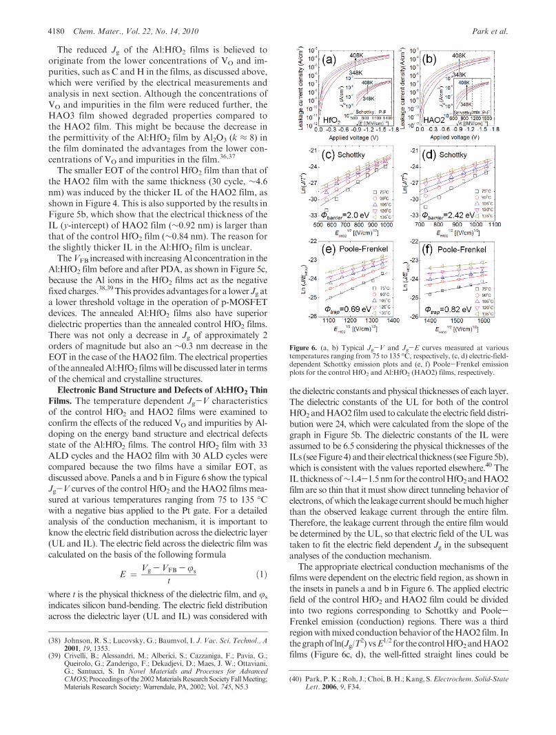
Figure 6. (a, b) Typical Jg-V and Jg-E curves measured at varioustemperatures ranging from 75 to 135 �C, respectively, (c, d) electric-field-dependent Schottky emission plots and (e, f) Poole-Frenkel emissionplots for the control HfO2 and Al:HfO2 (HAO2) films, respectively.
(38) Johnson, R. S.; Lucovsky, G.; Baumvol, I. J. Vac. Sci. Technol., A2001, 19, 1353.
(39) Crivelli, B.; Alessandri, M.; Alberici, S.; Cazzaniga, F.; Pavia, G.;Queirolo, G.; Zanderigo, F.; Dekadjevi, D.; Maes, J. W.; Ottaviani,G.; Santucci, S. In Novel Materials and Processes for AdvancedCMOS; Proceedings of the 2002MaterialsResearchSociety FallMeeting;Materials Research Society: Warrendale, PA, 2002; Vol. 745, N5.3
(40) Park, P.K.; Roh, J.; Choi, B.H.; Kang, S.Electrochem. Solid-StateLett. 2006, 9, F34.
Article Chem. Mater., Vol. 22, No. 14, 2010 4181
obtained in the low-field regions from ∼0.31 to ∼0.98 MV/cm, which corresponds to the applied voltage from approxi-mately -0.1 to approximately -0.7 V for the control HfO2
film, and from ∼0.45 to ∼1.11 MV/cm, which correspondsto the applied voltage from approximately-0.1 to approxi-mately -0.7 V for the HAO2 films. In these E regions,Schottky emissionwas found to be the dominant conductionmechanism. Schottky emission can be described as follows
J ¼ A�T2exp½ð- qðφB -ffiffiffiffiffiffiffiffiffiffiffiffiffiffiffiffiqE=4επ
pÞÞ=kT � ð2Þ
where A* is the effective Richardson constant, and ε and k
are the dynamic dielectric constant and the Boltzmann
constant, respectively. The ε value obtained from a fit of
Schottky emission ranged from ∼4.03 and ∼4.82, which is
similar to the theoretical value (n2 ≈ 4.0, n is the refractive
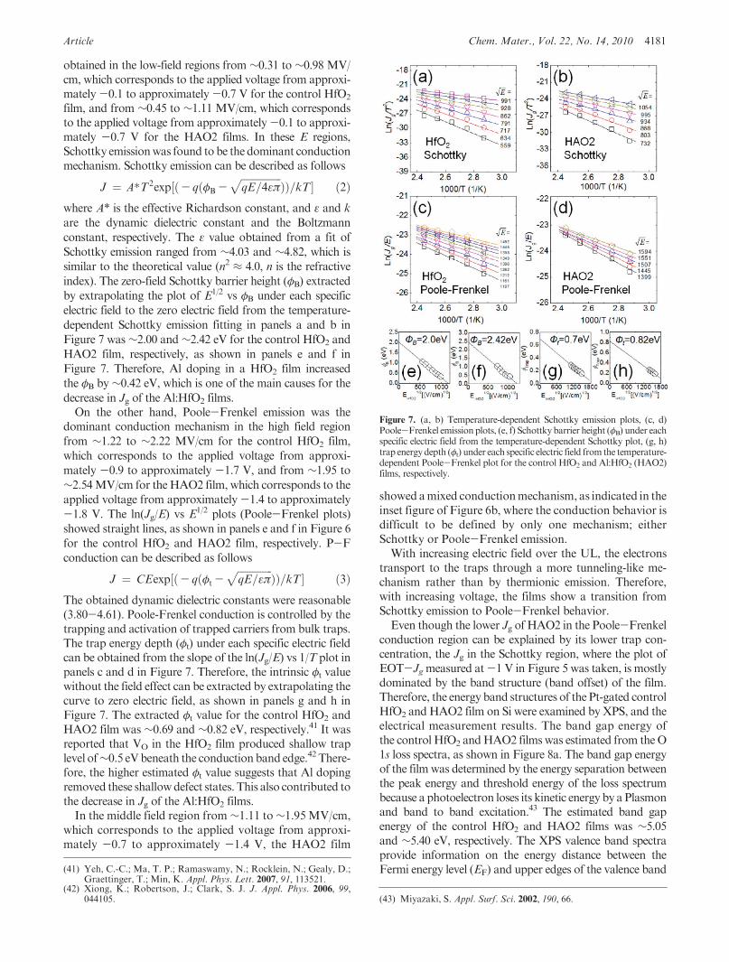
index). The zero-field Schottky barrier height (φB) extracted
by extrapolating the plot of E1/2 vs φB under each specific
electric field to the zero electric field from the temperature-
dependent Schottky emission fitting in panels a and b in
Figure 7 was ∼2.00 and∼2.42 eV for the control HfO2 and
HAO2 film, respectively, as shown in panels e and f in
Figure 7. Therefore, Al doping in a HfO2 film increased
the φB by ∼0.42 eV, which is one of the main causes for the
decrease in Jg of the Al:HfO2 films.On the other hand, Poole-Frenkel emission was the
dominant conduction mechanism in the high field region
from ∼1.22 to ∼2.22 MV/cm for the control HfO2 film,
which corresponds to the applied voltage from approxi-
mately -0.9 to approximately -1.7 V, and from ∼1.95 to
∼2.54MV/cm for theHAO2 film, which corresponds to the
applied voltage from approximately-1.4 to approximately
-1.8 V. The ln(Jg/E) vs E1/2 plots (Poole-Frenkel plots)
showed straight lines, as shown in panels e and f in Figure 6
for the control HfO2 and HAO2 film, respectively. P-F
conduction can be described as follows
J ¼ CEexp½ð- qðφt -ffiffiffiffiffiffiffiffiffiffiffiffiffiffiqE=επ
pÞÞ=kT � ð3Þ
The obtained dynamic dielectric constants were reasonable(3.80-4.61). Poole-Frenkel conduction is controlled by thetrapping and activation of trapped carriers from bulk traps.The trap energy depth (φt) under each specific electric fieldcan be obtained from the slope of the ln(Jg/E) vs 1/T plot inpanels c and d in Figure 7. Therefore, the intrinsic φt valuewithout the field effect can be extracted by extrapolating thecurve to zero electric field, as shown in panels g and h inFigure 7. The extracted φt value for the control HfO2 andHAO2 film was ∼0.69 and ∼0.82 eV, respectively.41 It wasreported that VO in the HfO2 film produced shallow traplevel of∼0.5 eVbeneath the conduction band edge.42 There-fore, the higher estimated φt value suggests that Al dopingremoved these shallowdefect states. This also contributed tothe decrease in Jg of the Al:HfO2 films.In the middle field region from∼1.11 to∼1.95MV/cm,
which corresponds to the applied voltage from approxi-mately -0.7 to approximately -1.4 V, the HAO2 film
showed amixed conductionmechanism, as indicated in theinset figure of Figure 6b, where the conduction behavior isdifficult to be defined by only one mechanism; eitherSchottky or Poole-Frenkel emission.With increasing electric field over the UL, the electrons
transport to the traps through a more tunneling-like me-chanism rather than by thermionic emission. Therefore,with increasing voltage, the films show a transition fromSchottky emission to Poole-Frenkel behavior.Even though the lower Jg of HAO2 in the Poole-Frenkel
conduction region can be explained by its lower trap con-centration, the Jg in the Schottky region, where the plot ofEOT-Jgmeasured at-1 V in Figure 5 was taken, is mostlydominated by the band structure (band offset) of the film.Therefore, the energy band structures of the Pt-gated controlHfO2 andHAO2 film on Si were examined by XPS, and theelectrical measurement results. The band gap energy ofthe control HfO2 andHAO2 films was estimated from theO1s loss spectra, as shown in Figure 8a. The band gap energyof the filmwas determined by the energy separation betweenthe peak energy and threshold energy of the loss spectrumbecause a photoelectron loses its kinetic energy by aPlasmonand band to band excitation.43 The estimated band gapenergy of the control HfO2 and HAO2 films was ∼5.05and ∼5.40 eV, respectively. The XPS valence band spectraprovide information on the energy distance between theFermi energy level (EF) and upper edges of the valence band
Figure 7. (a, b) Temperature-dependent Schottky emission plots, (c, d)Poole-Frenkel emission plots, (e, f) Schottkybarrier height (φB) under eachspecific electric field from the temperature-dependent Schottky plot, (g, h)trap energydepth (φt) under each specific electric field fromthe temperature-dependent Poole-Frenkel plot for the control HfO2 and Al:HfO2 (HAO2)films, respectively.
(41) Yeh, C.-C.; Ma, T. P.; Ramaswamy, N.; Rocklein, N.; Gealy, D.;Graettinger, T.; Min, K. Appl. Phys. Lett. 2007, 91, 113521.
(42) Xiong, K.; Robertson, J.; Clark, S. J. J. Appl. Phys. 2006, 99,044105. (43) Miyazaki, S. Appl. Surf. Sci. 2002, 190, 66.
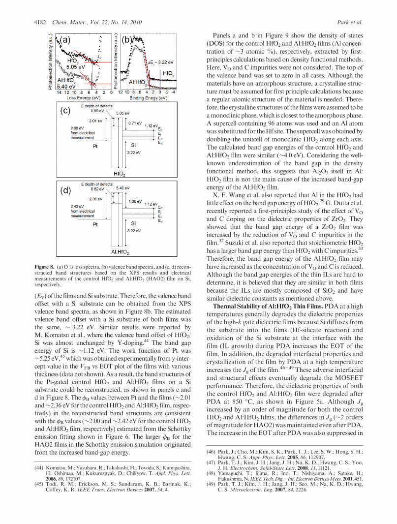
4182 Chem. Mater., Vol. 22, No. 14, 2010 Park et al.
(EV) of the filmsandSi substrate.Therefore, thevalencebandoffset with a Si substrate can be obtained from the XPSvalence band spectra, as shown in Figure 8b. The estimatedvalence band offset with a Si substrate of both films wasthe same, ∼ 3.22 eV. Similar results were reported byM. Komatsu et al., where the valence band offset of HfO2/Si was almost unchanged by Y-doping.44 The band gapenergy of Si is ∼1.12 eV. The work function of Pt was∼5.25 eV,45whichwas obtained experimentally fromy-inter-cept value in the VFB vs EOT plot of the films with variousthickness (datanot shown).Asa result, thebandstructuresofthe Pt-gated control HfO2 and Al:HfO2 films on a Sisubstrate could be reconstructed, as shown in panels c andd in Figure 8. The φB values between Pt and the films (∼2.01and∼2.36 eV for the controlHfO2 andAl:HfO2 film, respec-tively) in the reconstructed band structures are consistentwith theφB values (∼2.00 and∼2.42 eV for the controlHfO2
and Al:HfO2 film, respectively) estimated from the Schottkyemission fitting shown in Figure 6. The larger φB for theHAO2 films in the Schottky emission simulation originatedfrom the increased band-gap energy.
Panels a and b in Figure 9 show the density of states
(DOS) for the control HfO2 and Al:HfO2 films (Al concen-
tration of ∼3 atomic %), respectively, extracted by first-
principles calculations based on density functional methods.
Here, VO and C impurities were not considered. The top of
the valence band was set to zero in all cases. Although the
materials have an amorphous structure, a crystalline struc-
ture must be assumed for first principle calculations because
a regular atomic structure of the material is needed. There-
fore, the crystalline structuresof the filmswereassumed tobe
amonoclinic phase,which is closest to the amorphousphase.
A supercell containing 96 atoms was used and an Al atom
was substituted for theHf site.The supercellwasobtainedby
doubling the unitcell of monoclinic HfO2 along each axis.
The calculated band gap energies of the control HfO2 and
Al:HfO2 film were similar (∼4.0 eV). Considering the well-
known underestimation of the band gap in the density
functional method, this suggests that Al2O3 itself in Al:
HfO2 film is not the main cause of the increased band-gap
energy of the Al:HfO2 film.X. F. Wang et al. also reported that Al in the HfO2 had
little effect on the band gap energy ofHfO2.29G.Dutta et al.
recently reported a first-principles study of the effect of VO
and C doping on the dielectric properties of ZrO2. They
showed that the band gap energy of a ZrO2 film was
increased by the reduction of VO and C impurities in the
film.32 Suzuki et al. also reported that stoichiometric HfO2
has a larger band gap energy thanHfO2withC impurities.33
Therefore, the band gap energy of the Al:HfO2 film may
have increased as the concentration of VO andC is reduced.
Although the band gap energies of the thin ILs are hard to
determine, it is believed that they are similar in both films
because the ILs are mostly composed of SiO2 and have
similar dielectric constants as mentioned above.Thermal Stability of Al:HfO2Thin Films.PDAat a high
temperatures generally degrades the dielectric properties
of the high-k gate dielectric films because Si diffuses from
the substrate into the films (Hf-silicate reaction) and
oxidation of the Si substrate at the interface with the
film (IL growth) during PDA increases the EOT of the
film. In addition, the degraded interfacial properties and
crystallization of the film by PDA at a high temperature
increases the Jg of the film.46-49 These adverse interfacial
and structural effects eventually degrade the MOSFET
performance. Therefore, the dielectric properties of both
the control HfO2 and Al:HfO2 film were degraded afterPDA at 850 �C, as shown in Figure 5a. Although Jgincreased by an order of magnitude for both the controlHfO2 and Al:HfO2 films, the differences in Jg (∼2 ordersofmagnitude forHAO2)wasmaintained even after PDA.The increase in the EOTafter PDAwas also suppressed in
Figure 8. (a)O 1s loss spectra, (b) valence band spectra, and (c, d) recon-structed band structures based on the XPS results and electricalmeasurements of the control HfO2 and Al:HfO2 (HAO2) film on Si,respectively.
(44) Komatsu,M.;Yasuhara,R.;Takahashi,H.;Toyoda, S.;Kumigashira,H.; Oshimaa, M.; Kukuruznyak, D.; Chikyow, T. Appl. Phys. Lett.2006, 89, 172107.
(45) Todi, R. M.; Erickson, M. S.; Sundaram, K. B.; Barmak, K.;Coffey, K. R. IEEE Trans. Electron Devices 2007, 54, 4.
(46) Park, J.; Cho, M.; Kim, S. K.; Park, T. J.; Lee, S. W.; Hong, S. H.;Hwang, C. S. Appl. Phys. Lett. 2005, 86, 112907.
(47) Park, T. J.; Kim, J. H.; Jang, J. H.; Na, K. D.; Hwang, C. S.; Yoo,J. H. Electrochem. Solid-State Lett. 2008, 11, H121.
(48) Yamaguchi, T.; Iijima, R.; Ino, T.; Nishiyama, A.; Satake, H.;Fukushima,N. IEEETech.Dig.-Int.ElectronDevicesMeet.2001, 451.
(49) Park, T. J.; Kim, J. H.; Jang, J. H.; Seo, M.; Na, K. D.; Hwang,C. S. Microelectron. Eng. 2007, 84, 2226.
Article Chem. Mater., Vol. 22, No. 14, 2010 4183
case of the Al:HfO2 films (∼0.2 nm) compared to thecontrol HfO2 film (∼0.5 nm) as shown in Figure 5a.The crystalline and chemical structures of the Al:HfO2
films were analyzed to explain the improvement in thermal
stabilityof electrical properties against degradationbyPDA.The chemical structures of the filmswere examined bySIMS
depth profiling for the control HfO2 and HAO2 film beforeand after PDA, as shown in Figure 10. PDA reduced the
concentration of H impurity in both films. However, thecontrol HfO2 and HAO2 film showed similar chemical
structural changes after PDA. The change in the Al profilein the film after PDA was also negligible. Considering that
the Jg level of the film was determined mainly by the C andVO concentration in the film, the lack of a difference in the
chemical structural changes by PDA is consistent with thefact that the differences in Jg (∼2 orders of magnitude for
HAO2) between the control HfO2 andHAO2 film had beenpreserved, even after PDA.The EOT increase during the PDA is suppressed by the
increased permittivity of the film or the suppressed Hf-
silicate reaction and IL growth. It was reported that dopedHfO2andZrO2 filmshavea tetragonal or cubicphase,which
has a larger permittivity (J30) than a monoclinic phase
(j20).21-24 The diffraction patterns (DP) and HRTEM
images of the annealed Al:HfO2 films were examined to
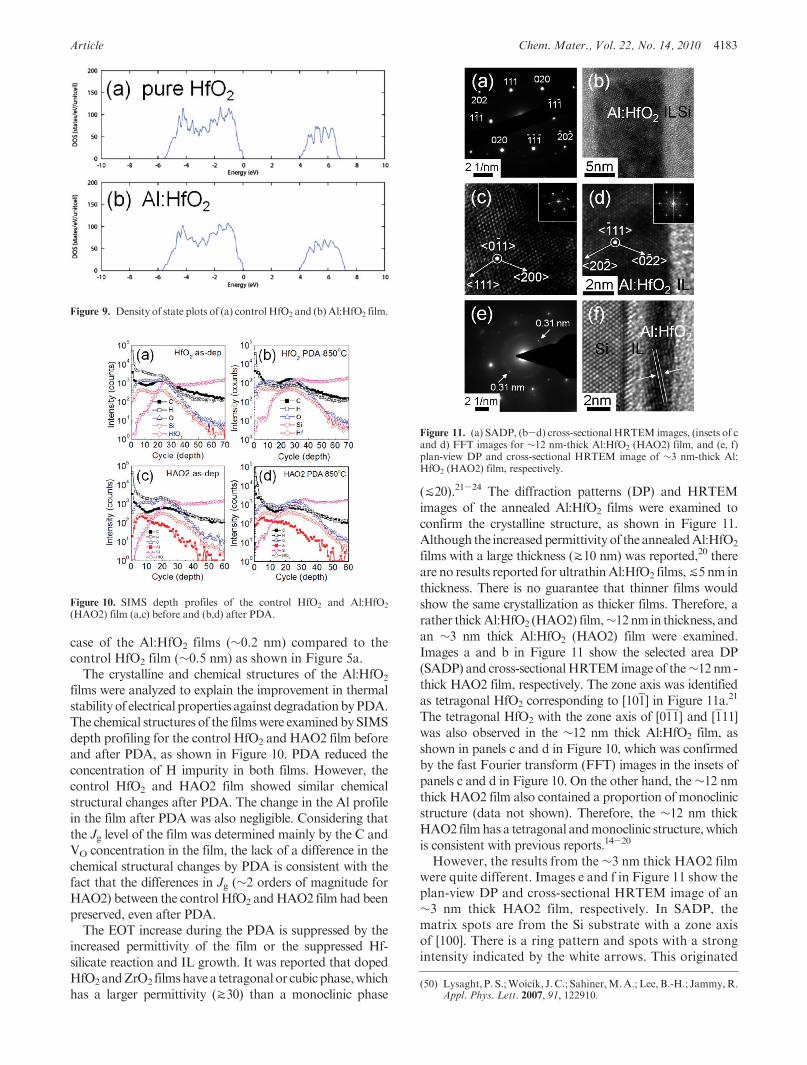
confirm the crystalline structure, as shown in Figure 11.
Although the increasedpermittivity of the annealedAl:HfO2
films with a large thickness (J10 nm) was reported,20 there
are no results reported for ultrathinAl:HfO2 films,j5 nm in
thickness. There is no guarantee that thinner films would
show the same crystallization as thicker films. Therefore, a
rather thickAl:HfO2 (HAO2) film,∼12nm in thickness, and
an ∼3 nm thick Al:HfO2 (HAO2) film were examined.
Images a and b in Figure 11 show the selected area DP
(SADP) and cross-sectionalHRTEM image of the∼12 nm -
thick HAO2 film, respectively. The zone axis was identified
as tetragonal HfO2 corresponding to [101] in Figure 11a.21
The tetragonal HfO2 with the zone axis of [011] and [111]
was also observed in the ∼12 nm thick Al:HfO2 film, as
shown in panels c and d in Figure 10, which was confirmed
by the fast Fourier transform (FFT) images in the insets of
panels c and d in Figure 10. On the other hand, the∼12 nmthick HAO2 film also contained a proportion of monoclinic
structure (data not shown). Therefore, the ∼12 nm thick
HAO2 filmhas a tetragonal andmonoclinic structure,which
is consistent with previous reports.14-20
However, the results from the ∼3 nm thick HAO2 filmwere quite different. Images e and f in Figure 11 show theplan-view DP and cross-sectional HRTEM image of an∼3 nm thick HAO2 film, respectively. In SADP, thematrix spots are from the Si substrate with a zone axisof [100]. There is a ring pattern and spots with a strongintensity indicated by the white arrows. This originated
Figure 9. Density of state plots of (a) control HfO2 and (b) Al:HfO2 film.
Figure 10. SIMS depth profiles of the control HfO2 and Al:HfO2
(HAO2) film (a,c) before and (b,d) after PDA.
Figure 11. (a) SADP, (b-d) cross-sectional HRTEM images, (insets of cand d) FFT images for ∼12 nm-thick Al:HfO2 (HAO2) film, and (e, f)plan-view DP and cross-sectional HRTEM image of ∼3 nm-thick Al:HfO2 (HAO2) film, respectively.
(50) Lysaght, P. S.;Woicik, J. C.; Sahiner,M.A.; Lee, B.-H.; Jammy,R.Appl. Phys. Lett. 2007, 91, 122910.
4184 Chem. Mater., Vol. 22, No. 14, 2010 Park et al.
from the lattice-space of 0.31 nm, which corresponds tothe (111) plane of a monoclinic HfO2.
50 A 0.31 nm latticefringe was also observed in the HRTEM image of the∼3 nm-thick HAO2 film, as shown in Figure 11f. As theplan-view SADP covers a large area (40 μm in diameter),this strongly suggests that most of the ∼3 nm thick HfO2
film remained in the monoclinic structure even after Aldoping. This might be because the ultrathin HAO2 film isinfluenced mainly by the Si substrate, such as Si diffusioninto the film and the stress field from the Si substrate.Hence, the superior electrical properties of the ultrathinHAO2 films after PDA cannot be explained by theincreased permittivity of the films.Therefore, the suppressed increases in the EOT of
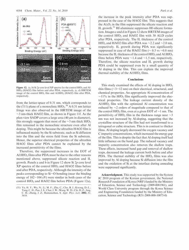
Al:HfO2 films after PDAmust be due to the other reasonsmentioned above, suppressed silicate reaction and ILgrowth. Panels a and b in Figure 12 show Si 2p core levelXP spectra of the control HfO2 and HAO2 films beforeand after PDA, respectively. Although the intensity of thepeaks corresponding to Si-O bonding (near the bindingenergy of 102-104 eV) were similar in both cases of thecontrol HfO2 and HAO2 film before PDA (Figure 12a),
the increase in the peak intensity after PDA was sup-pressed in the case of the HAO2 film. This suggests thatthe Al2O3 in the film suppressed the silicate reaction andIL growth.51 Hf-aluminate suppresses Hf-silicate forma-tion. Images c and d inFigure 12 showHRTEM images ofthe control HfO2 and HAO2 film with 30 ALD cyclesafter PDA, respectively. The IL thickness of the controlHfO2 and HAO2 film after PDA was ∼2.2 and ∼2.0 nm,respectively. IL growth during PDA was significantlysuppressed in case of the HAO2 film (∼ 0.5 vs ∼0.8 nm)because the IL thickness of the control HfO2 andAl:HfO2
films before PDA were ∼1.4 and ∼1.5 nm, respectively.Therefore, the silicate reaction and IL growth duringPDA could be suppressed even by a small quantity ofAl doping in the film. This can explain the improvedthermal stability of the Al:HfO2 films.
Conclusions
This study examined the effects of Al doping in HfO2
thin films (∼3-12 nm) on their electrical, structural, andchemical properties. An appropriate Al concentration of∼11% in the HfO2 film significantly improved the elec-trical properties. The leakage current density of theAl:HfO2 film with the optimized Al concentration wasreduced by ∼2 orders of magnitude compared to that ofthe control HfO2 film, even at a given EOT of∼1 nm. Thepermittivity of HfO2 film in the thickness range near ∼3nm was not increased by Al-doping, suggesting that thecrystalline structure of the film had not transformed to atetragonal or cubic structure. This is in contrast to thickerfilms. Al doping largely decreased the oxygen vacancy andC impurity concentrations, which increased the energy gapof the film. This is despite the fact that Al doping itself hadlittle influence on the band gap. The reduced vacancy andimpurity concentration also removes the shallow traps.These effects, increased band gap and removal of shallowtraps, decreased the leakage current both before and afterPDA. The thermal stability of the HfO2 films was alsoimproved by Al doping because Si diffusion into the filmand the oxidation of Si at the interface during annealingwere suppressed significantly.
Acknowledgment.This study was supported by the SystemIC 2010 program of the Korean government, the NationalResearchFoundation ofKorea (NRF) funded by theMinistryof Education, Science and Technology (2009-0081961), andWorld Class University program through the Korea Scienceand Engineering Foundation funded by the Ministry of Edu-cation, Science and Technology (R31-2008-000-10075-0)
Figure 12. (a, b) Si 2p core level XP spectra for the control HfO2 and Al:HfO2 (HAO2) film before and after PDA, respectively, (c, d) HRTEMimage of the control HfO2 film and Al:HfO2 (HAO2) film after PDA,respectively.
(51) Yu, H. Y.; Wu, N.; Li, M. F.; Zhu, C.; Cho, B. J.; Kwong, D.-L.;Tung, C. H.; Pan, J. S.; Chai, J. W.; Wang,W. D.; Chi, D. Z.; Ang,C. H.; Zheng, J. Z.; Ramanathan, S. Appl. Phys. Lett. 2002, 81,3618.