Reconfigurable Blocker-Tolerant RF Front-end Filter with Tunable...
4
Reconfigurable Blocker-Tolerant RF Front-end Filter with Tunable Notch for Active Cancellation of Transmitter Leakage in FDD Receivers M. Naimul Hasan, Qun Jane Gu and Xiaoguang Liu School of Electrical and Computer Engineering, University of California Davis, California, USA Email: [email protected] Abstract— A tunable N-path filter with an adaptive integrated notch is demonstrated for active cancellation of transmitter self-interference in frequency division duplexing (FDD) cellular systems. The proposed filter is a combination of N-path bandpass filter and a N-path bandstop filter, with the center frequency of the bandstop filter is tuned to the transmitting frequency to suppress transmit leakage. The passband of the filter is tunable from 0.4 GHz to 1.4 GHz. The gain of the filter is 17 dB. The rejection of the filter is 74.5 dB, where the notch is created. The NF of the filter is from 3.8–4.7 dB over the whole tuning range. The total power consumption of the filter is 36.4–56 mW. The channel bandwidth is 6.4 MHz and the out-of-band IIP3 is 21.2 dBm. I. I NTRODUCTION The growing demand of highly integrated multiband receivers for fourth-generation (4G)/fifth-generation (5G) wireless systems has driven the development of widely tunable filters for software defined radios. To reduce the cost and size of the transceiver chips, multiple dedicated narrowband radios must be replaced with one widely tunable radio. Off- chip, high-Q surface acoustic wave (SAW) filters are dedicated to suppress any out-of-band blockers in a conventional nar- rowband transceiver design. On the other hand, a wideband design has no selectivity and must withstand strong blockers as well as the wanted signal. In a frequency division duplexing system, the transmit (TX) signal is the most dominant blocker for the receiver. Several architectures have been proposed to handle large out-of-band (OOB) blockers and typically focus on 0-dBm continuous wave (CW) blockers. An out-of- band blocker is introduced at a frequency offset of 100 MHz in a long-term evaluation receiver, through TX leakage and TX self-interference as shown in Fig. 1 [1]. The frequency duplexer provides an isolation of 50 dB, which reduces the 30 dBm TX signal to -20 dBm in the primary receiver. Recent publications have shown tunable duplexers with high isolation between the transmit and receive signal paths [2]. On the other hand, the mobile device allows only 15 dB isolation between multiple antennas in a wireless system [1]. As a result, the received signal power is 12 dBm to secondary receivers, which significantly increases the IIP3 requirements. In a conventional architecture, a fixed SAW filter is inserted to suppress the TX leakage by 40 dB, and therefore, the OOB blocker power is reduced to -28 dBm as shown in Fig. 1(a) and the IIP3 15 dB Isolation 12 dBm PA LNA 1W (+30 dBm) -20 dBm -3 dB -50 dB 27 dBm Duplexer 40 dB SAW 12 dBm (a) Conventional Architecture f RX3 f TX1 f RX3 f TX1 f RX2 f TX1 (b) Proposed Architecture f RX1 f TX1 -28 dBm Primary receiver Secondary receivers Fig. 1. Proposed TX leakage suppression (a) conventional architecture with SAW filter (b) proposed architecture with integrated notch. requirement is relaxed. However, a fixed frequency SAW filter cannot be utilized in a wideband receiver. Several architectures have been proposed to handle TX leakage in multiband radios. A combination of bandpass and band-reject filtering is independently proposed in [1], [3] to suppress TX leakage. The filter in [1] can only suppress the TX leakage when the frequency difference between TX and RX is at least 100 MHz, due to the wide bandwidth of the filter and the power consumption of the filter is high. A blocker resilient wideband receiver is proposed in [4], with two point cancellation of TX leakage and TX noise in receive band. However, this technique rely on precise amplitude and phase matching, which is sensitive to process, voltage and temperature variations. On chip bandpass filters with inte- grated tunable notch are presented in [1], [5]. However, the power consumption of the filters is high. A wideband LNA is proposed in [6] for digital TV applications. Due to the use
Transcript of Reconfigurable Blocker-Tolerant RF Front-end Filter with Tunable...
Reconfigurable Blocker-Tolerant RF Front-endFilter with Tunable Notch for Active Cancellation
of Transmitter Leakage in FDD ReceiversM. Naimul Hasan, Qun Jane Gu and Xiaoguang Liu
School of Electrical and Computer Engineering, University of California Davis, California, USAEmail: [email protected]
Abstract— A tunable N-path filter with an adaptive integratednotch is demonstrated for active cancellation of transmitterself-interference in frequency division duplexing (FDD) cellularsystems. The proposed filter is a combination of N-path bandpassfilter and a N-path bandstop filter, with the center frequencyof the bandstop filter is tuned to the transmitting frequency tosuppress transmit leakage. The passband of the filter is tunablefrom 0.4 GHz to 1.4 GHz. The gain of the filter is 17 dB. Therejection of the filter is 74.5 dB, where the notch is created. TheNF of the filter is from 3.8–4.7 dB over the whole tuning range.The total power consumption of the filter is 36.4–56 mW. Thechannel bandwidth is 6.4 MHz and the out-of-band IIP3 is 21.2dBm.
I. INTRODUCTION
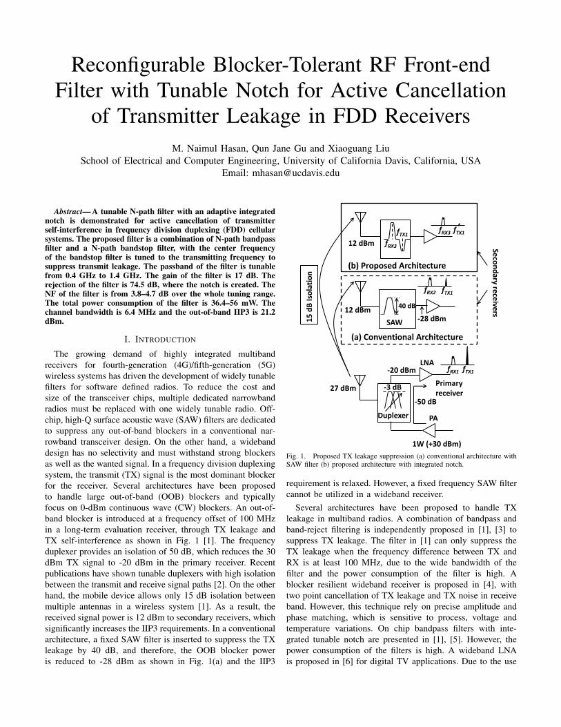
The growing demand of highly integrated multibandreceivers for fourth-generation (4G)/fifth-generation (5G)wireless systems has driven the development of widely tunablefilters for software defined radios. To reduce the cost andsize of the transceiver chips, multiple dedicated narrowbandradios must be replaced with one widely tunable radio. Off-chip, high-Q surface acoustic wave (SAW) filters are dedicatedto suppress any out-of-band blockers in a conventional nar-rowband transceiver design. On the other hand, a widebanddesign has no selectivity and must withstand strong blockersas well as the wanted signal. In a frequency division duplexingsystem, the transmit (TX) signal is the most dominant blockerfor the receiver. Several architectures have been proposedto handle large out-of-band (OOB) blockers and typicallyfocus on 0-dBm continuous wave (CW) blockers. An out-of-band blocker is introduced at a frequency offset of 100 MHzin a long-term evaluation receiver, through TX leakage andTX self-interference as shown in Fig. 1 [1]. The frequencyduplexer provides an isolation of 50 dB, which reduces the 30dBm TX signal to -20 dBm in the primary receiver. Recentpublications have shown tunable duplexers with high isolationbetween the transmit and receive signal paths [2]. On the otherhand, the mobile device allows only 15 dB isolation betweenmultiple antennas in a wireless system [1]. As a result, thereceived signal power is 12 dBm to secondary receivers, whichsignificantly increases the IIP3 requirements. In a conventionalarchitecture, a fixed SAW filter is inserted to suppress the TXleakage by 40 dB, and therefore, the OOB blocker poweris reduced to -28 dBm as shown in Fig. 1(a) and the IIP3
15
dB
Iso
lati
on
12 dBm
PA
LNA
1W (+30 dBm)
-20 dBm
-3 dB
-50 dB
27 dBm
Duplexer
40 dB
SAW
12 dBm
(a) Conventional Architecture
fRX3
fTX1 fRX3 fTX1
fRX2 fTX1
(b) Proposed Architecture
fRX1 fTX1
-28 dBm
Primary receiver
Seco
nd
ary rece
ivers
Fig. 1. Proposed TX leakage suppression (a) conventional architecture withSAW filter (b) proposed architecture with integrated notch.
requirement is relaxed. However, a fixed frequency SAW filtercannot be utilized in a wideband receiver.
Several architectures have been proposed to handle TXleakage in multiband radios. A combination of bandpass andband-reject filtering is independently proposed in [1], [3] tosuppress TX leakage. The filter in [1] can only suppress theTX leakage when the frequency difference between TX andRX is at least 100 MHz, due to the wide bandwidth of thefilter and the power consumption of the filter is high. Ablocker resilient wideband receiver is proposed in [4], withtwo point cancellation of TX leakage and TX noise in receiveband. However, this technique rely on precise amplitude andphase matching, which is sensitive to process, voltage andtemperature variations. On chip bandpass filters with inte-grated tunable notch are presented in [1], [5]. However, thepower consumption of the filters is high. A wideband LNAis proposed in [6] for digital TV applications. Due to the use

...
s1
50 Vin
s3 s1
s3 s2
s4 s2s2
s4 s3
s1
s1
s3 s4
s2s4
c1 c1 c1 c1
gm1
s3
s3
s1
s1 s4
s4s2
s2c3 c3
Buffer
Buffer
Vout+
Vout-
s1 s1
s3s3
s2 s2
s4 s4
s3
s1
s3
s1
s4 s4
s2 s2
gm
gm
RL RL
c2
c2
c2
c2
1: 2
Vb1
Vb2
Vb3
Vb4
Bandstop Filter
Bandpass Filter
Bandpass Filter
gm1
Fig. 2. Proposed Bandpass filter schematic with integrated tunable notch.
(a) (b)
×270.6
0.06
Vin
VDD
Vout
×271.4
0.06
4k 4k
VDD
Vin+ 4
0.13 4
0.13
4
0.06
Vin-
VBIAS
Vout+Vout-
4
0.5
4
0.5
10k
×7
×30 ×30
×7
×30
Fig. 3. (a) A self-biased inverter used as gm1 (b) gm cells used in bandstopfilter.
of low supply voltage in modern CMOS process, a 0 dBmblocker will cause the LNA to clip, which increases noise anddistortion in the receiver.
A low power tunable bandpass filter with an integratedadaptive notch is presented in this paper. The filter willbe used in front of the LNA to handle large out-of-bandblockers as shown in Fig. 1(b). In section II, the design of theproposed bandpass filter is demonstrated. Section III describesthe simulation results and section IV concludes the paper.
II. PROPOSED BANDPASS FILTER ARCHITECTURE
The proposed filter consists of two bandpass sections andone bandstop section between them. The bandpass sectionsare implemented with R-C configuration of N-path filters andthe bandstop section is implemented with C-R configurationof N-path filters. The schematic of the proposed filter isshown in Fig. 2. A transconductor cell (gm1) is used afterthe first bandpass section to increase the gain of the filteras well as to reduce the noise from subsequent stages. Thecenter frequency of the bandstop filter is shifted by usingfeedforward and feedback gm cells. The gain of the bandstopsection can be changed by varying the load resistance RL. Thetransistor sizes used in the bandpass and bandstop sectionsare (W/L = 50 µm/60 nm) and (W/L = 40 µm/60 nm) re-
𝑪𝟐 𝑹𝑳
−𝟏
𝒋𝒈𝒎
𝑽𝒃𝟏
…
−𝟏
𝒋𝒈𝒎
𝑽𝒃𝟒 𝑪𝟐
𝑹𝑳
𝑪𝟐 𝑹𝑳
𝑽𝒃𝟏
…
𝑽𝒃𝟒 𝑪𝟐
𝑹𝑳
𝑪𝟐 𝑹𝑳
𝟏
𝒋𝒈𝒎
𝑽𝒃𝟏
…
𝟏
𝒋𝒈𝒎
𝑽𝒃𝟒 𝑪𝟐
𝑹𝑳
𝒇𝒊𝒏 around 𝒇𝑳𝑶 𝒇𝒊𝒏 around 𝟐𝒇𝑳𝑶 𝒇𝒊𝒏 around 𝟑𝒇𝑳𝑶
Fig. 4. Effective baseband admittance YBB(s, k)(1 ≤ k ≤ 3) for thebandstop filter shown in Fig. 2.
spectively. The baseband capacitors used in the bandpassand bandstop sections are 50 pF and 8 pF, respectively.Two self-biased inverters are used as gm1 to increase thegain of the filter, as shown in Fig. 3(a). A fully differentialarchitecture with resistive common mode feedback is used asthe transconductor cell (gm) in the bandstop filter as shown inFig. 3(b) . The nominal value of load resistance, RL = 10 kΩ.
A. Bandstop Filter Frequency Shifting
The primary idea of shifting the center frequency of abandstop filter with respect to the switching frequency fLO
is described here. gm − C technique is used to shift thecenter frequency of the bandstop filter as shown in Fig. 2.Feedforward and feedback gm cells are used at the basebandnodes (Vbi, 1 ≤ i ≤ 4) with differential capacitor basebandimpedances to shift the center frequency of the bandstop filter.As a result, a bandstop filter can be cascaded with a bandpassfilter to create an overall bandpass filter with an integratednotch.
The phase relation between the baseband node volt-ages, Vbi of a N-path filter can be described byVbx = Vbye
jkπ2 ×(x−y), [1 ≤ (x, y) ≤ N ], where N is the num-
ber of clock phases. The equation only holds when fin isaround kfLO. It is possible to find an effective baseband ad-

Vin
gm1
Rs
Rsw ro1 RL
Vout
NC1
Rsw
NC1
Rsw
√2
NC2-jgm
Fig. 5. A simplified half circuit schematic of the filter to calculate the overalltransfer function of the filter (N=4).
0.90 0.95 1.00 1.05 1.10 1.15 1.20 1.25
-10
0
10
AV
(dB
)
Frequency (GHz)
Mathematical derivation Spectre RF simulation
Fig. 6. Comparing SpectreRF simulation of the bandstop filter shown in Fig.2 with mathematical derivation (5). (Rsw = 20Ω, gm = 6.1 mS,RL =10 kΩ and C2 = 8 pF.)
mittance YBB(s, k) due to the gm cells between the basebandnode voltages. YBB(s, k) for fin around kfLO[(1 ≤ k ≤N −1)] for the bandstop filter shown in Fig. 2 is illustrated inFig. 4. From Fig. 4, YBB(s, 1) = C2(s−jωBB), YBB2 = sC2
and YBB(s, 3) = C2(s + jωBB), where ωBB = gm/2C2.As a result, the center frequency of the baseband admittanceis modified from 0 to ωBB for YBB(s, 1) and −ωBB forYBB(s, 3). Due to the exploitation of differential gms withgood common mode rejection, the center frequency of thebaseband admittance does not change for YBB(s, 2). In N-path filters, the effective baseband admittance characteristicswill be translated to kfLO, k ∈ Z. Therefore, the center fre-quency of the filter shifts upward around fLO and downwardaround 3fLO by gm/4πC2. The filter operates similar to aconventional 4-path filter for input frequencies around 2fLO.
The bandstop filter transfer function is given by
H(s) =Vout(s)
Vin(s)= 1−
∞∑k=−∞
sinc2(kπ
N
)×G(s−jkωLO, k)
(1)where G(s, k) is a HPF due to the combination of a basebandadmittance YBB(s, k) and a load resistance and described in
G(s, k) =NRL
NRTYBB(s, k) + 1(2)
where N=4 in our case and RT = RL +Rsw
The transfer function of the filter around fLO can be foundby using two terms (k = −1, 1) in (3)
H(s) = 1− 8
π2× (G(s− jωLO, 1) +G(s− jωLO,−1)) (3)
whereG(s,±1) =
NRLYBB(s,±1)
1 +NRTYBB(s,±1)
=4RL(sC2 ± jgm)
1 + 4RT (sC2 ± jgm)
(4)
0.90 0.95 1.00 1.05 1.10-60
-40
-20
0
20
Av (
dB)
Frequency (GHz)
Proposed Filter 6th order Bandpass Filter
74.5 dB
Fig. 7. Comparison between all pole filter and the proposed filter.
Therefore, H(s) will be
H(s) = 1− 8
π2×(
4RLC2(s− jωLO)− j4gmRL
1 + 4RTC2(s− jωLO)− j4gmRT
)− 8
π2×(
4RLC2(s+ jωLO) + j4gmRL
1 + 4RTC2(s+ jωLO) + j4gmRT
)
= 1− 16RL
π2RT×s2 +
(gm2C2
+ ωLO
)2
s2 +2s
RTC2+ ω2
LO
(5)The center frequency of the bandstop filter is shifted togm
4πC2. Depending on whether gm is positive or negative, the
frequency shifting is negative or positive, respectively. As aresult, the notch frequency can be shifted to either side of thefilter center frequency.
B. Transfer Function of the Filter
The overall transfer function of the filter can be calculatedfrom Fig. 5. Assuming, RL Rsw, we can use (5), to findthe transfer function of the bandstop filter by replacing RL
with Rsw+jωNC1
jωNC1. The overall transfer function is described
in (6), where
H1(s) = gm1ro1 ×Rsw(1 + sNC1)
Rsw + sNC1(Rs +Rsw)(7)
The transfer function of the filter is compared with theSpectreRF simulation in Fig. 6 for Rsw = 20 Ω, RL = 10 kΩ,C2 = 8 pF, and gm = 6.1 mS. The notch frequency is shiftedin the SpectreRF simulation due to the bottom plate parasiticcapacitance of the baseband capacitance.
III. SIMULATION RESULTS
The proposed filter is designed using 65 nm CMOStechnology. The baseband capacitors are realized with MIMcapacitors and the resistors are realized with N+ poly resistor
0.9 1.0 1.1
-50
-40
-30
-20
-10
0
10
20
Av (
dB)
Frequency (GHz)
D=15% D=20% D=25% D=30%
Fig. 8. The transfer function of the filter with duty cycle variations.
Htot(s) = H1(s)
1 −16
π2×
1 + sNC2Rsw
1 + sNRsw(C2 + C1)×s2 +
(gm2C2
+ ωLO
)2s2 + 2s
RTC2+ ω2
LO
(6)
0.90 0.95 1.00 1.05 1.10-60
-50
-40
-30
-20
-10
0
10
20
S21
(dB
)
Frequency (GHz)
C=6 pF C=8 pF C=10 pF C=12 pF C=16 pF
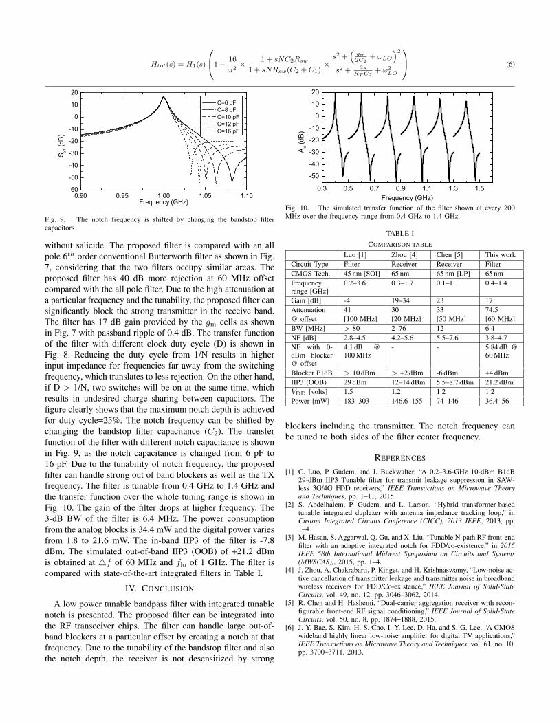
Fig. 9. The notch frequency is shifted by changing the bandstop filtercapacitors
without salicide. The proposed filter is compared with an allpole 6th order conventional Butterworth filter as shown in Fig.7, considering that the two filters occupy similar areas. Theproposed filter has 40 dB more rejection at 60 MHz offsetcompared with the all pole filter. Due to the high attenuation ata particular frequency and the tunability, the proposed filter cansignificantly block the strong transmitter in the receive band.The filter has 17 dB gain provided by the gm cells as shownin Fig. 7 with passband ripple of 0.4 dB. The transfer functionof the filter with different clock duty cycle (D) is shown inFig. 8. Reducing the duty cycle from 1/N results in higherinput impedance for frequencies far away from the switchingfrequency, which translates to less rejection. On the other hand,if D > 1/N, two switches will be on at the same time, whichresults in undesired charge sharing between capacitors. Thefigure clearly shows that the maximum notch depth is achievedfor duty cycle=25%. The notch frequency can be shifted bychanging the bandstop filter capacitance (C2). The transferfunction of the filter with different notch capacitance is shownin Fig. 9, as the notch capacitance is changed from 6 pF to16 pF. Due to the tunability of notch frequency, the proposedfilter can handle strong out of band blockers as well as the TXfrequency. The filter is tunable from 0.4 GHz to 1.4 GHz andthe transfer function over the whole tuning range is shown inFig. 10. The gain of the filter drops at higher frequency. The3-dB BW of the filter is 6.4 MHz. The power consumptionfrom the analog blocks is 34.4 mW and the digital power variesfrom 1.8 to 21.6 mW. The in-band IIP3 of the filter is -7.8dBm. The simulated out-of-band IIP3 (OOB) of +21.2 dBmis obtained at 4f of 60 MHz and flo of 1 GHz. The filter iscompared with state-of-the-art integrated filters in Table I.
IV. CONCLUSION
A low power tunable bandpass filter with integrated tunablenotch is presented. The proposed filter can be integrated intothe RF transceiver chips. The filter can handle large out-of-band blockers at a particular offset by creating a notch at thatfrequency. Due to the tunability of the bandstop filter and alsothe notch depth, the receiver is not desensitized by strong
0.3 0.5 0.7 0.9 1.1 1.3 1.5
-50
-40
-30
-20
-10
0
10
20
Av (
dB)
Frequency (GHz)Fig. 10. The simulated transfer function of the filter shown at every 200MHz over the frequency range from 0.4 GHz to 1.4 GHz.
TABLE ICOMPARISON TABLE
Luo [1] Zhou [4] Chen [5] This workCircuit Type Filter Receiver Receiver FilterCMOS Tech. 45 nm [SOI] 65 nm 65 nm [LP] 65 nmFrequencyrange [GHz]
0.2–3.6 0.3–1.7 0.1–1 0.4–1.4
Gain [dB] -4 19–34 23 17Attenuation 41 30 33 74.5@ offset [100 MHz] [20 MHz] [50 MHz] [60 MHz]BW [MHz] > 80 2–76 12 6.4NF [dB] 2.8–4.5 4.2–5.6 5.5–7.6 3.8–4.7NF with 0-dBm blocker@ offset
4.1 dB @100 MHz
- - 5.84 dB @60 MHz
Blocker P1dB > 10 dBm > +2 dBm -6 dBm +4 dBmIIP3 (OOB) 29 dBm 12–14 dBm 5.5–8.7 dBm 21.2 dBmVDD [volts] 1.5 1.2 1.2 1.2Power [mW] 183–303 146.6–155 74–146 36.4–56
blockers including the transmitter. The notch frequency canbe tuned to both sides of the filter center frequency.
REFERENCES
[1] C. Luo, P. Gudem, and J. Buckwalter, “A 0.2–3.6-GHz 10-dBm B1dB29-dBm IIP3 Tunable filter for transmit leakage suppression in SAW-less 3G/4G FDD receivers,” IEEE Transactions on Microwave Theoryand Techniques, pp. 1–11, 2015.
[2] S. Abdelhalem, P. Gudem, and L. Larson, “Hybrid transformer-basedtunable integrated duplexer with antenna impedance tracking loop,” inCustom Integrated Circuits Conference (CICC), 2013 IEEE, 2013, pp.1–4.
[3] M. Hasan, S. Aggarwal, Q. Gu, and X. Liu, “Tunable N-path RF front-endfilter with an adaptive integrated notch for FDD/co-existence,” in 2015IEEE 58th International Midwest Symposium on Circuits and Systems(MWSCAS),, 2015, pp. 1–4.
[4] J. Zhou, A. Chakrabarti, P. Kinget, and H. Krishnaswamy, “Low-noise ac-tive cancellation of transmitter leakage and transmitter noise in broadbandwireless receivers for FDD/Co-existence,” IEEE Journal of Solid-StateCircuits, vol. 49, no. 12, pp. 3046–3062, 2014.
[5] R. Chen and H. Hashemi, “Dual-carrier aggregation receiver with recon-figurable front-end RF signal conditioning,” IEEE Journal of Solid-StateCircuits, vol. 50, no. 8, pp. 1874–1888, 2015.
[6] J.-Y. Bae, S. Kim, H.-S. Cho, I.-Y. Lee, D. Ha, and S.-G. Lee, “A CMOSwideband highly linear low-noise amplifier for digital TV applications,”IEEE Transactions on Microwave Theory and Techniques, vol. 61, no. 10,pp. 3700–3711, 2013.