Reconfigurable RRAM-based computing: A Case study for ...
89
Rochester Institute of Technology RIT Scholar Works eses esis/Dissertation Collections 8-1-2012 Reconfigurable RM-based computing: A Case study for reliability enhancement Mahew Catanzaro Follow this and additional works at: hp://scholarworks.rit.edu/theses is esis is brought to you for free and open access by the esis/Dissertation Collections at RIT Scholar Works. It has been accepted for inclusion in eses by an authorized administrator of RIT Scholar Works. For more information, please contact [email protected]. Recommended Citation Catanzaro, Mahew, "Reconfigurable RM-based computing: A Case study for reliability enhancement" (2012). esis. Rochester Institute of Technology. Accessed from
Transcript of Reconfigurable RRAM-based computing: A Case study for ...

Rochester Institute of TechnologyRIT Scholar Works
Theses Thesis/Dissertation Collections
8-1-2012
Reconfigurable RRAM-based computing: A Casestudy for reliability enhancementMatthew Catanzaro
Follow this and additional works at: http://scholarworks.rit.edu/theses
This Thesis is brought to you for free and open access by the Thesis/Dissertation Collections at RIT Scholar Works. It has been accepted for inclusionin Theses by an authorized administrator of RIT Scholar Works. For more information, please contact [email protected].
Recommended CitationCatanzaro, Matthew, "Reconfigurable RRAM-based computing: A Case study for reliability enhancement" (2012). Thesis. RochesterInstitute of Technology. Accessed from

Reconfigurable RRAM-basedComputing: A Case Study for Reliability
Enhancementby
Matthew M. Catanzaro
A Thesis Submitted in Partial Fulfillment of the Requirements for theDegree of Master of Science
in Computer Engineering
Supervised by
Assistant Professor Dr. Dhireesha KudithipudiDepartment of Computer EngineeringKate Gleason College of Engineering
Rochester Institute of TechnologyRochester, New York
August 2012
Approved by:
Dr. Dhireesha Kudithipudi, Assistant ProfessorThesis Advisor, Department of Computer Engineering
Dr. Sonia Lopez Alarcon, Assistant ProfessorCommittee Member, Department of Computer Engineering
Dr. Roy Melton, Senior LecturerCommittee Member, Department of Computer Engineering

Thesis Release Permission Form
Rochester Institute of TechnologyKate Gleason College of Engineering
Title:
Reconfigurable RRAM-based Computing: A Case Study for ReliabilityEnhancement
I, Matthew M. Catanzaro, hereby grant permission to the Wallace Memo-rial Library to reproduce my thesis in whole or part.
Matthew M. Catanzaro
Date

iii
Abstract
Emerging hybrid-CMOS nanoscale devices and architectures offer greater
degree of integration and performance capabilities. However, the high power
densities, hard error frequency, process variations, and device wearout affect
the overall system reliability. Reactive design techniques, such as redun-
dancy, account for component failures by mitigating them to prevent sys-
tem failures. These techniques incur high area and power overhead. This
research focuses on exploring hybrid CMOS/Resistive RAM (RRAM) ar-
chitectures that enhance the system reliability by performing computation
in RRAM cache whenever CMOS logic units fail, essentially masking the
area overhead of redundant logic when not in use. The proposed designs are
validated using the Gem5 performance simulator and McPAT power simu-
lator running single-core SPEC2006 benchmarks and multi-core PARSEC
benchmarks.
The simulation results are used to evaluate the efficacy of reliability
enhancement techniques using RRAM. The average runtime when using
RRAM for functional unit replacement was between ∼1.5 and ∼2.5 times
longer than the baseline for a single-core architecture, ∼1.25 and ∼2 times

iv
longer for an 8-core architecture, and ∼1.2 and ∼1.5 times longer for a
16-core architecture. Average energy consumption when using RRAM for
functional unit replacement was between ∼2 and ∼5 times more than the
baseline for a single-core architecture, and ∼1.25 and ∼2.75 times more
for multi-core architectures. The performance degradation and energy con-
sumption increase is justified by the prevention of system failure and en-
hanced reliability. Overall, the proposed architecture shows promise for use
in multi-core systems. Average performance degradation decreases as more
cores are used due to more total functional units being available, preventing
a slow RRAM functional unit from becoming a bottleneck.

v
Contents
Abstract . . . . . . . . . . . . . . . . . . . . . . . . . . . . . . . iii
1 Background . . . . . . . . . . . . . . . . . . . . . . . . . . . 11.1 Introduction . . . . . . . . . . . . . . . . . . . . . . . . . . 11.2 Reliability . . . . . . . . . . . . . . . . . . . . . . . . . . . 3
1.2.1 Hard Errors . . . . . . . . . . . . . . . . . . . . . . 41.2.2 Reliability Theory . . . . . . . . . . . . . . . . . . 51.2.3 Majority Voter Circuits . . . . . . . . . . . . . . . . 61.2.4 Standby Redundancy . . . . . . . . . . . . . . . . . 71.2.5 Dynamic Reliability Management (DRM) . . . . . . 8
1.3 Resistive RAM . . . . . . . . . . . . . . . . . . . . . . . . 101.4 Hybrid CMOS/RRAM Architectures . . . . . . . . . . . . . 13
1.4.1 Crossbar Architecture . . . . . . . . . . . . . . . . 131.4.2 One Transistor and One Resistor (1T1R) Architecture 15
2 Related Work . . . . . . . . . . . . . . . . . . . . . . . . . . 162.1 Memory-Based Computing . . . . . . . . . . . . . . . . . . 162.2 Spin-Torque Transfer Magnetoresistive RAM Computing . . 182.3 Reliability Metrics . . . . . . . . . . . . . . . . . . . . . . 19
2.3.1 Mean Time to Failure . . . . . . . . . . . . . . . . . 192.3.2 Failures in Time . . . . . . . . . . . . . . . . . . . 21
3 Proposed Architecture Design . . . . . . . . . . . . . . . . . 233.1 Test-Case Architecture Implementation . . . . . . . . . . . 25

vi
3.2 RRAM Arrays . . . . . . . . . . . . . . . . . . . . . . . . . 283.3 RRAM Controller . . . . . . . . . . . . . . . . . . . . . . . 31
4 LUT Logic Mapping . . . . . . . . . . . . . . . . . . . . . . 344.1 Integer ALU . . . . . . . . . . . . . . . . . . . . . . . . . . 354.2 Integer Multiplier . . . . . . . . . . . . . . . . . . . . . . . 374.3 Floating-Point Adder . . . . . . . . . . . . . . . . . . . . . 39
5 Simulation Platform . . . . . . . . . . . . . . . . . . . . . . 425.1 Gem5 Simulator . . . . . . . . . . . . . . . . . . . . . . . . 43
5.1.1 Gem5 Modifications . . . . . . . . . . . . . . . . . 445.2 McPAT Simulator . . . . . . . . . . . . . . . . . . . . . . . 45
5.2.1 McPAT Modifications . . . . . . . . . . . . . . . . 465.3 SPEC2006 Benchmark Suite . . . . . . . . . . . . . . . . . 475.4 PARSEC Benchmark Suite . . . . . . . . . . . . . . . . . . 48
6 Simulation Results and Analysis . . . . . . . . . . . . . . . . 496.1 Single Core Simulations . . . . . . . . . . . . . . . . . . . 496.2 Multi-core Simulations . . . . . . . . . . . . . . . . . . . . 60
7 Conclusions . . . . . . . . . . . . . . . . . . . . . . . . . . . 70
8 Future Work . . . . . . . . . . . . . . . . . . . . . . . . . . 72
Bibliography . . . . . . . . . . . . . . . . . . . . . . . . . . . . 74

vii
List of Tables
1.1 Characteristics of Memory Device Parameters at Nanoscale . 12
3.1 Alpha Processor Conversions . . . . . . . . . . . . . . . . . 273.2 Test-Case Architecture Implementations . . . . . . . . . . . 273.3 RRAM Functional Data [43] . . . . . . . . . . . . . . . . . 30
4.1 Functional Unit Decomposition Statistics . . . . . . . . . . 354.2 LUT-Based Floating-Point Adder Decomposition . . . . . . 41
5.1 Functional Unit Pool Options in the O3CPU . . . . . . . . . 445.2 Cache Configuration Options in the O3CPU . . . . . . . . . 455.3 SPEC2006 Benchmark Attributes . . . . . . . . . . . . . . 475.4 PARSEC Benchmark Attributes . . . . . . . . . . . . . . . 48
6.1 Single Core Simulation Configurations . . . . . . . . . . . . 516.2 Multi-Core Simulation Configurations . . . . . . . . . . . . 61

viii
List of Figures
1.1 Triple Redundant Group of Functional Units with Voter Logic 71.2 Standby Set of Redundant Functional Units . . . . . . . . . 81.3 Bipolar Memristor Curve with ±2 V Threshold Switching . 121.4 Sneak Paths Inherent in the Crossbar Architecture . . . . . . 141.5 1T1R Architecture . . . . . . . . . . . . . . . . . . . . . . 15
2.1 Representation of STT-MRAM Processor Pipeline [21] . . . 19
3.1 Representation of the Proposed Hybrid CMOS/RRAM Ar-chitecture for Reliability Enhancement . . . . . . . . . . . . 24
3.2 Alpha 21264 Microarchitecture [12] . . . . . . . . . . . . . 263.3 RRAM Controller Block Diagram . . . . . . . . . . . . . . 33
4.1 RRAM Array Representation for 4-Bit ALU . . . . . . . . . 364.2 Block-Level Schematic of LUT-Based 32-Bit ALU Design . 374.3 32-Bit LUT-Based Multiplier Design . . . . . . . . . . . . . 384.4 32-Bit Floating-Point Addition Process . . . . . . . . . . . . 40
5.1 Representation of the Custom Tuned Simulation Framework 42
6.1 SPEC2006 Benchmark Profiles . . . . . . . . . . . . . . . . 506.2 SPEC2006 Benchmark Energy Usage for Different Cache
Levels . . . . . . . . . . . . . . . . . . . . . . . . . . . . . 526.3 SPEC2006 Benchmark Timing for Different Cache Levels . 536.4 SPEC2006 Benchmark Runtime With L2 RRAM Cache and
Replaced LUT-Based FUs . . . . . . . . . . . . . . . . . . 55

ix
6.5 SPEC2006 Benchmark Runtime With L3 RRAM Cache andReplaced LUT-Based FUs . . . . . . . . . . . . . . . . . . 56
6.6 SPEC2006 Benchmark Energy With L2 RRAM Cache andReplaced LUT-Based FUs . . . . . . . . . . . . . . . . . . 57
6.7 SPEC2006 Benchmark Energy With L3 RRAM Cache andReplaced LUT-Based FUs . . . . . . . . . . . . . . . . . . 58
6.8 SPEC2006 Benchmark Energy With L3 RRAM Cache andReplaced LUT-Based FUs . . . . . . . . . . . . . . . . . . 60
6.9 PARSEC Benchmark Runtime for L2 SRAM and L2 RRAMCaches . . . . . . . . . . . . . . . . . . . . . . . . . . . . . 62
6.10 PARSEC Benchmark Energy for L2 SRAM and L2 RRAMCaches . . . . . . . . . . . . . . . . . . . . . . . . . . . . . 63
6.11 PARSEC Benchmark Runtime With 8 Cores, L2 RRAMand Replaced LUT-Based FUs . . . . . . . . . . . . . . . . 64
6.12 PARSEC Benchmark Runtime With 16 Cores, L2 RRAMand Replaced LUT-Based FUs . . . . . . . . . . . . . . . . 65
6.13 PARSEC Benchmark Energy With 8 Cores, L2 RRAM andReplaced LUT-Based FUs . . . . . . . . . . . . . . . . . . 67
6.14 PARSEC Benchmark Energy With 16 Cores, L2 RRAM andReplaced LUT-Based FUs . . . . . . . . . . . . . . . . . . 68

1
Chapter 1
Background
1.1 Introduction
Hard error frequency in complementary metal-oxide-semiconductor (CMOS)
integrated circuits increases exponentially as CMOS technology scales, which
is a growing concern for reliable system design [1][23]. The number of hard
errors that lead to failures have increased by 274% from 180nm to 65nm
technology [38]. CMOS scaling increases hard error rates due to smaller
devices having increased power and heat densities, accelerating wear-out of
the silicon. Increasing transistor counts inherently inflate the error rate as
well. Significant research efforts have been made in the domain of hardware
reliability, and hard error prevention and correction in CMOS [14][37][40].
Unfortunately, current reliability mechanisms incur large area and power
overheads, as much as N times the area and power for N redundant units
[2].

2
Recently, novel devices have been explored to serve as a possible supple-
ment or even a replacement for CMOS technology in the near future, mainly
in the field of memory. New memory devices include phase change RAM
(PRAM) [20], ferroelectric RAM (FeRAM) [3], magneto-resistive RAM
(MRAM) [15] and resistive RAM (RRAM) [22]. While many of these new
devices suffer from problems such as slow speed, large area, high power and
lack of CMOS compatibility, few show promise as a replacement memory
technology. RRAM is one such technology, as it offers high density, recon-
figurability, non-volatility, and CMOS compatibility. RRAM has already
shown that it can be applied to many different application domains such as
temperature sensing [30] and specifically for this research, reconfigurable
logic [42].
Hybrid architectures using novel RRAM devices have also been explored.
RRAM architectures that have been fully realized are the hybrid CMOS/RRAM
architectures [9]. These architectures are advantageous because of their re-
configurability, high density (4F 2, where F is the feature size) and low idle
energy. Researchers have been focusing on the design, implementation, and
realization of such hybrid architectures [41] but not much attention is given
to the adoption of these architectures for fault-tolerance or enhancing the
reliability of these architectures.

3
This research explores hybrid CMOS/RRAM architectures that can uti-
lize RRAM as both memory and logic. CMOS functional units can be im-
plemented in RRAM if a hard error occurs, to enhance reliability by pre-
venting system failure. Functional units are investigated to determine which
functions can be implemented as RRAM LUT-based logic, and which ones
cannot. Finally, hybrid CMOS/RRAM architectures are tested and analyzed
to determine the efficacy of utilizing them for reliability enhancement.
The remainder of this document is organized as follows: This chapter
presents a background on hard errors, CMOS reliability techniques, and
RRAM including CMOS/RRAM hybrid architectures. Chapter 2 discusses
existing work relevant to this thesis. Chapter 3 presents the architectures
used, while Chapter 4 presents the method of implementing computational
functions in RRAM. Chapter 5 explains the simulation platform and bench-
marks used to gather results, while Chapter 6 discusses and analyzes the
results. Chapter 7 summarizes the results and draws conclusions, and fi-
nally Chapter 8 presents possible future work on this topic.
1.2 Reliability
A reliable processor should incorporate mechanisms for the prevention of
errors, detection of errors, the correction of those errors, or a combination

4
of all three. Preventing errors inherently reduces the risk of failures. Er-
ror detection mechanisms allow errors to be found and isolated when they
occur. Correcting errors that have occurred prevents them from causing
failures. This section discusses hard errors and reliability techniques used
in current CMOS systems.
1.2.1 Hard Errors
Hard errors are caused by defects or faults in the silicon of CMOS systems.
They tend to be permanent because the problem lies in the physical structure
of the hardware. There are two types of hard errors, extrinsic and intrinsic.
Extrinsic errors are known as “early infant mortality” errors because they
occur soon after operation begins. The root cause of extrinsic errors are
problems in the fabrication process such as misaligned lithography masks,
manifesting themselves as short circuits or open circuits. [37]
Intrinsic errors tend to manifest themselves long into the lifetime of a
system, and are caused by wear-out over time. Error rates caused by wear-
out can be accelerated by subjecting a system to heavy stress often or over
long periods of time. Preventing and correcting these hard errors are nec-
essary for having a reliable system. CMOS reliability techniques have been

5
researched and implemented in CMOS, but many have significant draw-
backs that can be avoided through the use of CMOS/RRAM architectures
such as high area overhead.
1.2.2 Reliability Theory
Hard error correction improves the reliability of a system by detecting hard
errors and implementing solutions to prevent total system failure. One of the
universal reliability circuits proposed by J. VonNuemann as early as 1956
[40], the majority organ or majority logic gate, can be used to synthesize
reliable circuits from unreliable systems. The three input signal probabilities
feeding in to the majority logic gate, η1, η2, and η3, represent the upper
bounds for these lines to be carrying the wrong data. The upper bound of
at least two lines carrying the wrong data (which are in the same state of
excitation) is set in Equation 1.1.
e = η1η2 + η1η3 + η2η3 − 2η1η2η3 (1.1)
In general, the system will be reliable if e is relatively small. Such a
system works well for mitigating hard errors, when the probability of failure
of the components is less than 0.5, which is more than sufficient for present
day systems. The majority logic gate can be used in reliable architectures to

6
pass through the most common output, generally being the correct output.
This theory is the basis for majority voter circuits.
1.2.3 Majority Voter Circuits
A majority voter circuit uses redundant functional units to perform the same
logic function, where the outputs are sent to a majority logic gate, and the
most common result among them is used [40]. If η represents the upper
bound for the probability of error in a functional unit O, a triple redundant
group of functional unitsO∗ with majority logic gate has probability of error
η∗, where ε is the definite probability of an error, shown in Equation 1.2. The
majority logic gate is often called voter logic, hence the name majority voter
circuit. If a hard error occurs in one of the functional units, the redundant
units still have the majority, and the correct result is relayed to the system
output.
η∗ = ε+ (1− 2ε)(3η2 − 2η3) (1.2)
Figure 1.1 demonstrates the triple redundant group of functional units
O∗ with voter logic labeled as m. A system without redundant logic and
majority voter circuitry, or other mitigation techniques, can experience total
failure if a necessary/executive functional unit fails. Unfortunately, the cost

7
of having hard error reliable systems using redundancy is over N times the
amount of area and power for N repeated functional units and voting logic
[2].
O1
O2
O3
m
m
A
A
A
B
B
B
C
C
C
X1
X2
X3
Y3
Y2
Y1 X
Y
Figure 1.1: Triple Redundant Group of Functional Units with Voter Logic
Some fault-tolerant mechanisms used to improve hard error failures are
triple modular redundancy (TMR) and N-tuple modular redundancy (NMR)
[14]. TMR uses three redundant components that feed into voting logic,
while NMR uses N redundant components, usually an odd number, that
feed into voting logic. These techniques are the de-facto standard in several
mission-critical applications.
1.2.4 Standby Redundancy
Another technique that is similar to majority voting is standby redundancy,
as seen in Figure 1.2. Additional redundant components are implemented

8
and are all connected to a switching mechanism [11]. At any given mo-
ment, only one component is operational. When the currently operational
component fails, the switching mechanism switches to a redundant compo-
nent, whichs takes over the functional load. Although this technique incurs
a large area overhead, it has low power overhead because redundant logic is
either turned off or placed in a low power state when not in use.
O1
O2
O3
ABC
XYS S
Figure 1.2: Standby Set of Redundant Functional Units
1.2.5 Dynamic Reliability Management (DRM)
Hard error prevention improves the reliability of a system by extending the
lifetime of hardware through stress reduction. Dynamic reliability manage-
ment (DRM) is a technique that has been proven to improve reliability in
under-designed systems [37]. Most processors are over-designed. That is,
they are designed to operate at the worst case and can increase their per-
formance as long as they stay within reliability margins. Under-designed

9
systems are built to operate at expected, or normal utilization and temper-
ature, and have reduced overall system cost. Under-designed systems have
difficulty operating at worst case, but it is assumed that the DRM mecha-
nism has knowledge of the run-time behavior of every task, can determine
when the worst case will happen, and act accordingly.
DRM leverages the knowledge of application run-time behavior to de-
grade performance using techniques such as voltage and frequency scaling
and decreased system utilization in order to reduce system stress and pre-
vent prolonged stress from increasing hard error rates and damaging the sys-
tem. To predict the run-time system behavior accurately is a non-trivial task.
Since several of the prediction mechanisms are based on statistical analysis,
DRM might not be able to react in time for certain cases. Unexpected sys-
tem behavior could still raise the stress on components to dangerous levels
because DRM does not act. Another problem with DRM is that it does not
perform any error correction. Even though DRM takes preventative mea-
sures, once a hard error occurs, it cannot fix the issue.
Redundancy-based reliability enhancement mechanisms incur large area
overhead. With the new class of emerging 3D hybrid architectures, redun-
dancy can be applied hierarchically, and only when needed, to mitigate the
faults occurring from increasingly unreliable nanoscale devices. In par-
ticular, CMOS/RRAM hybrid architectures utilize the reconfigurability of

10
RRAM to perform both memory and logic, which leads to new opportuni-
ties in the fields of fault-tolerance and reliability.
1.3 Resistive RAM
In 1971, Leon Chua proposed a fourth basic circuit element, the memris-
tor [10]. Memristors were realized as nanoscale thin film devices by HP
Labs in 2008 [39] and have great potential to be used as non-volatile mem-
ory [22]. There are several materials with which memristive devices can
be fabricated such as titanium dioxide (TiO2), hafnium dioxide (HfO2) and
copper oxide (CuOx) [17]. Memristors are one of the primary devices cur-
rently used in RRAM fabrication because of their high density (4F 2, where
F is the feature size), low read energy, low leakage power, non-volatility,
high resistance ratio, and CMOS compatibility.
The memristor is a two-terminal memory device located between a top
and bottom electrode, where logic storage is resistance-based. The memory
device changes its resistance based on the electrical signal through it, and
retains its value while no electrical signal is applied. RRAM uses mem-
ristors as the underlying device in a crossbar architecture. The difference
between RRAM and other emerging memory technologies is that ferroelec-
tricity, magnetization, and phase change of material state are not involved

11
in the resistance changing process.
Resistance switching in RRAM devices can be either unipolar or bipolar.
Unipolar devices switch based on the magnitude of an applied voltage, and
are controlled by the amount of current allowed to flow. Unipolar devices
generally involve Joule heating, but are difficult to control due to current
compliance [25].
Bipolar devices switch based on both the magnitude and polarity of the
applied voltage. A large positive voltage changes a device to be in a low
resistance state, while a large negative voltage changes a device to be in a
high resistance state. Bipolar devices have voltage threshold characteris-
tics. Significant resistance switching will only occur if the magnitude of the
applied voltage exceeds the magnitude of the threshold value of identical
polarity [35]. In Figure 1.3, the positive and negative voltage thresholds for
a bipolar memristor can be seen at approximately ±2 V.
The International Technology Roadmap for Semiconductors (ITRS) states
that RRAM is comparable to other memory devices such as DRAM, SRAM
and NOR Flash [1]. Table 1.1 shows the non-volatility, scalability and small
feature size of RRAM compared to other memory devices. The access
speeds are improving in more recent realizations of these devices, using
new materials.
Peripheral and interface logic required for reading and writing data to the

12
Figure 1.3: Bipolar Memristor Curve with ±2 V Threshold Switching
Table 1.1: Characteristics of Memory Device Parameters at NanoscaleRRAM DRAM SRAM NOR Flash
Feature Size <30 nm 65 nm 45 nm 90 nm [A] Without charge appliedAccess Speed <3 ns <10 ns <1 ns 15 ns [B] With charge applied
Retention Time >10 years [A] 64 ms [A] [B] 10 years [A] [C] <1 V for writeOperating Voltage <0.5 V [C] 1.8 V 1 V 1.8 V [D] [D] 10 V for write
RRAM restricts, to a certain extent, the high density that can be achieved
[43]. To address this issue, it is possible to use multilevel RRAM memory,
where multiple bits can be represented by one memristor, which increases
the memory density by a factor of the number of levels [31]. Storing two bits
per memristor using four resistance levels doubles the total memory density.
An issue with multilevel RRAM memory is its small noise margins, where it

13
becomes significantly more difficult to represent a multi-bit logic state with
a resistance state correctly and confidently. The state is shifted up or down
undesirably with increasing ease as more levels are utilized.
Memristors are passive devices, therefore RRAM requires CMOS pe-
ripheral circuitry in order to operate. The necessity of CMOS circuitry
has led to hybrid CMOS/RRAM architectures becoming a focal point for
RRAM related research.
1.4 Hybrid CMOS/RRAM Architectures
Few hybrid CMOS/RRAM architectures have been proposed that have been
realized at the system level [8] [45] [24] [4]. Of these, the crossbar and
the one transistor and one resistor (1T1R) architecture have been widely
adopted due to their practicality.
1.4.1 Crossbar Architecture
In the crossbar architecture, RRAM devices are set between two parallel ar-
rays of nano-wires, which are placed 90 offset from one another, allowing
for maximum memory density. A problem with this architecture is the pres-
ence of sneak paths as shown in Figure 1.4, which create alternative current

14
paths through adjacent memory locations that should not be disturbed in the
current operation.
...
...
...
...
...
...
Desired Path Sneak Path
Figure 1.4: Sneak Paths Inherent in the Crossbar Architecture
Methods have been proposed to reduce the effects of sneak paths [45]
[24][28]. One such technique is V/2 voltage biasing, where unselected rows
and columns are biased to reduce current flow through adjacent devices,
minimizing disturbances. If the selected row is biased to a voltage V and
the selected column is biased to Gnd, the unselected rows and columns are
biased to a voltage V/2. The maximum voltage drop across any unselected
memristor is therefore V/2, below the voltage thresholds for resistance state
change.

15
1.4.2 One Transistor and One Resistor (1T1R) Architecture
The 1T1R architecture, as shown in Figure 1.5, solves the sneak path prob-
lem by integrating a CMOS transistor in series with the memristor. Each
transistor requires its own individual select wire, which allows current to
flow only through a selected memory device [4][29]. The problem with this
architecture is the reduction in memory density, negating one of the promi-
nent benefits of RRAM. The additional transistors and wiring for selecting
each individual element result in an increased area per bit, and overall mem-
ory density is limited by CMOS scaling.
This research uses the crossbar architecture because it provides the high-
est density and requires less CMOS circuitry compared to the 1T1R archi-
tecture. Area, timing, and power data has been published on this architec-
ture, and the results can be used for simulating this research [43].
6/ 6/ 6/%/ / %/ / %/ /
: / /
: / /
: / /
WL1
WL2
WL3
SL BL1 SL SLBL2 BL3
Figure 1.5: 1T1R Architecture
16
Chapter 2
Related Work
Some recent work has been focused on emerging ideas and devices such
as memory-based computing (MBC) and spin-torque transfer magnetore-
sistive RAM (STT-MRAM) computing for reliability enhancement and in-
volve techniques relevant to this research [34][21]. In this section, a detailed
description of both existing efforts and reliability metrics will be discussed.
2.1 Memory-Based Computing
Memory-based computing (MBC) is a technique that uses on-chip CMOS
cache to perform look-up table (LUT) based logic functions for reliability
enhancement [34]. Logic functions can be implemented in L1 or L2 SRAM
cache as needed if a computational unit becomes non-functional due to a

17
hard error or overheats due to heavy stress. Instead of throttling the perfor-
mance of a system under thermal stress by temporarily disabling an over-
heating functional unit, activity migration to the on-chip cache occurs. Ac-
tivity migration also improves reliability by implementing and performing
the operation of failed CMOS functional units in on-chip cache as LUT-
based logic, preventing system failure.
A problem with using MBC in L1 and L2 SRAM cache is that the re-
configuration subspace for logic is constrained by the small cache size, al-
though in most cases, the subspace is sufficient for logic reconfiguration.
Cache that is overwritten by a functional unit implementation must be re-
fetched if needed again. Therefore, the cache hit rates will be inadvertently
affected, degrading average access time, when a large subspace is reconfig-
ured. The remaining available cache space that can be used as memory is
now smaller, causing data to be overwritten more frequently and increasing
the miss rate. Another consideration is that on-chip SRAM cache is not lo-
cated in the same area as CMOS functional units on the chip, requiring long
wire lengths for getting result data to the integer and floating-point registers.

18
2.2 Spin-Torque Transfer Magnetoresistive RAM Comput-ing
A special case of MBC is spin-torque transfer magnetoresistive RAM (STT-
MRAM) computing. STT-MRAM is CMOS-compatible, leakage-resistant
and non-volatile magnetic memory technology. Authors in [21] have pro-
posed the use of STT-MRAM for both memory and computing. They fo-
cus on low-power, low cost, energy efficient multi-core systems using STT-
MRAM to scale systems smaller than the 45nm technology node. The idea
is to replace SRAM cache completely with STT-MRAM cache and CMOS
functional units with STT-MRAM LUT-based logic. The near-zero leak-
age STT-MRAM greatly reduces the power density compared to its CMOS
counterpart. Figure 2.1 shows the architectural pipeline used when imple-
menting STT-MRAM into a processor. All CMOS logic and functional units
are replaced with STT-MRAM LUT-based logic, while the caches and reg-
ister files are replaced with STT-MRAM memory arrays. ALUs remain im-
plemented in CMOS because their circuit complexity does not benefit from
using multiple small input width STT-MRAM LUTs.
The STT-MRAM architecture is similar to the 1T1R RRAM architecture
in that a transistor is used in series with the memory element, a magnetic
tunnel junction (MTJ). Unfortunately it allows maximum memory density

19
Figure 2.1: Representation of STT-MRAM Processor Pipeline [21]
of only 10F 2. The largest problem with STT-MRAM is its low resistance
ratio of 6.25kΩ/2.5kΩ (Rhigh/Rlow). A high resistance ratio is required
to ensure the correct value is read. If Rhigh and Rlow are very close, an
incorrect read is more prone to occur, making the system unreliable.
2.3 Reliability Metrics
Reliability of a system can be defined by the functional longevity of a system
without failing. The most common metrics to measure reliability are the
mean time to failure (MTTF) and failures in time (FIT) rate.
2.3.1 Mean Time to Failure
The expected lifetime of a processor is also known as the mean time to fail-
ure (MTTF). If a hard error occurs in a component that is not easily replaced,

20
the processor becomes unusable. The MTTF model consists of four primary
causes, or failure mechanisms, of CMOS failures. The first failure mecha-
nism is electromigration, which is the accumulation or depletion of metal
atoms in unwanted locations due to current flow. The second is stress mi-
gration, which is the accumulation or depletion of metal atoms in unwanted
locations due to mechanical stress and thermal expansion. The third failure
mechanism of CMOS failure is time-dependant dielectric breakdown, which
is when the gate oxide of a transistor wears down over time. The final cause
in the MTTF model is thermal cycling, which is a large fluctuation in tem-
perature due to changes to and from low-power modes or power on / power
off cycles. Thermal cycles impact a processor the most at solder joints,
where connections could break or short circuit. The failure mechanisms of
all components can be combined to form the MTTF of an entire processor
as shown in Equation 2.1, where j is the number of components, k is the list
of failure mechanisms, and λil is the failure rate of the ith component due to
the lth failure mechanism.
MTTFp =1∑j
i=1
∑kl=1 λil
(2.1)

21
2.3.2 Failures in Time
The failures in time (FIT) rate is more commonly used in industry because
it is less complex and more easily calculated via circuit level testing. The
low-level details of component material, temperature, and voltage are not
required. The FIT rate is simply the number of failures in 109 hours. This
metric can be calculated for individual components, or entire processors.
The FIT rate of a processor can be calculated from the FIT rates of indi-
vidual components as shown in Equation 2.2, where j is the number of
components, and FITratei is the FIT rate of the ith component.
FITratep =
j∑i=0
FITratei (2.2)
These reliability metrics are only useful when low-level implementation
and fabrication details are known or when systems are realized and able
to be run to gather reliability statistics. They are unable to be applied to
architectural simulations, although it can be assumed that FIT rates will
increase if hard errors are corrected and the system continues to operate
until a future failure.
The fundamental idea behind MBC, performing logic in memory using
LUT-based logic, is a key concept for this research. Using MBC in RRAM
instead of on-chip SRAM cache has a benefit of spatial locality, where the

22
replaced logic in RRAM can be physically close to the CMOS functional
units if used in a 3D integrated circuit (3D-IC). Additionally, RRAM’s high
density allows more memory capacity to be implemented in the same sized
area. The larger the cache, the less impact implementing a functional unit in
cache will have on the hit / miss rates. Integrating emerging memory devices
into CMOS systems to operate as cache and logic is a key concept for this
research as well. Using RRAM instead of STT-MRAM gives greater area
efficiency, and RRAM also has a higher resistance ratio of 500kΩ/10kΩ
(Rhigh/Rlow). This research also extends the STT-MRAM concept to utilize
emerging memory devices for reliability enhancement.

23
Chapter 3
Proposed Architecture Design
An overview of the proposed three dimensional integrated circuit (3D-IC)
architecture is shown in Figure 3.1. A CMOS computational layer is used
as tier one, and the RRAM is overlaid as tier two of the 3D stack. The
RRAM layer is implemented as a group of equally sized arrays, which will
be analyzed later in this chapter. The RRAM arrays are arranged in an
H-tree structure. This structure obtains equal wire lengths to each array,
maintaining equal read and write times.
The RRAM is stacked on top of the CMOS layer to improve the spatial
locality of replaced functional units. RRAM arrays directly above a failed
CMOS unit can be reconfigured to implement the replacement unit using
short wire lengths, keeping latency to a minimum.
Each RRAM array requires its own driver and selection circuitry imple-
mented in CMOS. Another benefit of having the RRAM as the second tier
of a 3D stack is for efficient implementation of the CMOS peripheral cir-
cuitry for each array. Again, this high spatial locality of CMOS circuitry to

24
RRAM arrays minimizes the effects of latency due to wire length.
The RRAM layer is used as the highest level of cache because it is slower
than on-chip SRAM cache, but faster than main memory accesses. The
cache level that RRAM is used for has no affect on the the way functional
units are implemented because the execution datapath is re-routed directly
to the RRAM layer. This chapter describes the details of the architectures
that are simulated, then analyzes the implementation of the RRAM arrays
and finally discusses requirements for the RRAM controller.
CMOS layer
RRAM Layer
Processor CoreL2
L3 T
ags L3
Tag
s RRAMController
L2 Tags
Cache
L2Cache
H-Tree
Figure 3.1: Representation of the Proposed Hybrid CMOS/RRAM Architecture for Relia-bility Enhancement

25
3.1 Test-Case Architecture Implementation
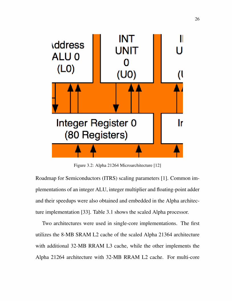
The CMOS core used in this work is simulated as an Alpha-like proces-
sor. The Alpha 21264 microarchitecure can be seen in Figure 3.2 [12]. The
pipeline provides out of order (O3) computing and can issue up to four in-
structions per cycle at a clock speed of 1.2 GHz. The functional units avail-
able are four integer arithmetic logic units (ALUs), one integer multiplier
associated with one of the integer ALUs, one floating-point ALU unit and
one floating-point multiplier. The integer and floating-point pipelines are
split, each with their own issue queues and result registers. L1 cache is split
into an instruction cache and a data cache, both of size 64 KB with 2-way
set associativitiy.
The Alpha 21364 processor was designed and fabricated for 180-nm
technology in 2003 and has a processing core identical to the 21264 ver-
sion [32]. Additional hardware added to the 21264 core to create the new
21364 model includes a 1.75-MB 8-way set associative on-chip L2 cache
with cache coherence hardware, two memory controllers, and a router to
create multi-core architectures easily using this processor. The router is re-
moved from single-core simulations because it is not utilized.
The Alpha architecture is scaled to 45nm using International Technology
26
Figure 3.2: Alpha 21264 Microarchitecture [12]
Roadmap for Semiconductors (ITRS) scaling parameters [1]. Common im-
plementations of an integer ALU, integer multiplier and floating-point adder
and their speedups were also obtained and embedded in the Alpha architec-
ture implementation [33]. Table 3.1 shows the scaled Alpha processor.
Two architectures were used in single-core implementations. The first
utilizes the 8-MB SRAM L2 cache of the scaled Alpha 21364 architecture
with additional 32-MB RRAM L3 cache, while the other implements the
Alpha 21264 architecture with 32-MB RRAM L2 cache. For multi-core

27
Table 3.1: Alpha Processor ConversionsItem Alpha 21364 Converted Alpha
Technology 180 nm 45 nmClock Speed 1.2 GHz 4 GHz
Supply Voltage 1.65 V 1.1 VInteger ALU 1 cycle 1 cycle
Integer Multiplier 7 cycles 4 cyclesFloating-Point Adder 4 cycles 4 cycles
Floating-Point Divider 15 cycles 20 cyclesFloating-Point Sqrt. 30 cycles 20 cycles
Floating-Point Multiplier 4 cycles 4 cyclesL1 Cache Speed 4 cycles 4 cycles
L1 Cache Size 64 kB 256 kBL2 Cache Speed 15 cycles 10 cycles
L2 Cache Size 1.75 MB 8 MB
simulations, both 8-core and 16-core systems are tested. The 8-core archi-
tecture has a shared 256-MB (32 MB× 8 cores) RRAM L2 cache, while the
16-core architecture has a shared 512-MB (32 MB × 16 cores) RRAM L2
cache. The differences in the simulated architectures is shown in Table 3.2.
Main memory capacity for each architecture is 2 GB, and the block size is
64 KB.
Table 3.2: Test-Case Architecture ImplementationsRRAM L3 Cache RRAM L2 Cache 8 Core 16 Core
L2 Cache 8 MB SRAM 32 MB RRAM 256 MB RRAM 512 MB RRAML3 Cache 32 MB RRAM None None None
Portions of RRAM are reconfigured to implement LUT-based logic when
hard errors occur in CMOS components. The reconfiguration is handled by
the RRAM controller, explained in section 4.3. Functional units that are

28
practical to implement as LUT-based logic are used in this research, such as
the integer ALU, the integer multiplier, and the floating-point adder. Func-
tional units that do not map into LUT-based logic, and are not attempted in
this experiment, involve operations such as shifting, division and the square
root.
All of the RRAM is used as cache in normal operation, when no hard er-
rors have occurred, to mask the area overhead of LUT-based logic. This mit-
igates the high area overhead incurred in traditional redundancy-based ma-
jority voting circuits and standby redundant circuits. Additionally, RRAM
has low leakage power and therefore reduced power overhead compared
to others. The size of RRAM cache is significantly larger than traditional
SRAM caches of the same area due to its high density. The reconfigured
portions of RRAM consume a small percentage of the cache, having lit-
tle impact on the miss ratio compared to MBC architectures using on-chip
SRAM cache.
3.2 RRAM Arrays
The maximum array size for an RRAM array is determined by the write
driver current, and the voltage biasing scheme used to prevent sneak path
current [43]. The V/2 biasing scheme is used to prevent significant sneak

29
path current; therefore the maximum driver current is represented in Equa-
tion 3.1, where Ireset is the reset current, Nr is the number of rows, and
ILRS(Vreset/2) is the current through a device in a low-resistance state (LRS)
with a Vreset/2 bias.
Idriver = Ireset + (Nr − 1)× ILRS(Vreset/2) (3.1)
Memristors are non-linear; that is, current through a memristor is not di-
rectly proportional to the voltage applied to it, because memristance (and
therefore resistance) is not a constant. A coefficient of non-linearity is used
for a V/p biasing scheme as shown in Equation 3.2, where Kr is the coeffi-
cient of non-linearity and RV/p and RV are static resistances of a memristor
biased at V/p and V respectively. In the case of this research, a p value of 2
is used for the V/2 biasing scheme.
Kr(p, V ) = p×RV/p
RV(3.2)
Using equations 3.1 and 3.2, the maximum number of rows and columns
can be calculated based on the driver current when all selected rows and
columns intersect at devices in the LRS. Equations 3.3 and 3.4 show this
relationship, where Nsc is the number of selected columns per row.

30
Nr = (IdriverIreset
− 1)×Kr(2, Vreset) + 1 (3.3)
Nc = (IdriverIreset
−Nsc)×Kr(2, Vreset) +Nsc (3.4)
Using the previous equations, the maximum array size was found to be
512 bits × 512 bits (32 KB). A 32-MB RRAM memory is designed using
the maximum sized arrays connected in an H-tree structure. Sensing and
read/write circuitry are interfaced from the CMOS layer. The read latency
for this architecture is 1.8 ns and the write latency is 200 ns as shown in
Table 3.3 [43].
Table 3.3: RRAM Functional Data [43]Read Latency (ns) 1.773
Write Latency (ns) 200.7Read Energy (nJ) 0.195
Write Energy (nJ) 25.81
The high write latency can be mitigated by using the cache inclusion
protocol, where every level of cache is a subset of each subsequent level
[18]. This means that a miss in the highest cache level gets written to all
levels of cache after being fetched from main memory. It can be assumed
that a request for the same data soon after the write would hit in a lower
cache level, while the data is still being written to the higher cache level by
the controller.

31
3.3 RRAM Controller
The controller, implemented in CMOS, handles the reading and writing to
the RRAM arrays. It is assumed that data can be fetched from main memory
in 64-KB blocks, common for all levels of cache in the architecture, and that
reads and writes can be performed in the form of a byte (8 bits), word (16
bits), long word (32 bits) or long long word (64 bits). In addition, because
the write time for RRAM is long, it is assumed that additional reads can
occur in arrays that are not currently being written to.
The controller also handles hard error detection in the CMOS functional
units. Error detection circuitry, such as “lazy error detection,” can detect
errors one cycle after the output arrives and has an area overhead as low as
33% of the functional unit with which it is associated [44]. Specific error
detection circuitry is not within the scope of this thesis, and the assump-
tion that error detection successfully occurs after an error manifests itself is
sufficient.
After an error is detected, the CPU stalls while the error correction pro-
cess occurrs. First, the program counter must be rolled back to the instruc-
tion prior to where the error occured. The controller then reconfigures the
portion of the RRAM arrays to implement a failed functional unit. This re-
configuration process includes writing LUT-based logic from memory to the

32
arrays and setting the control logic for additional CMOS circuitry, known as
“glue logic”, required to implement the failed unit. The execution datapath
is rerouted by the controller to use the LUT-based logic that has been im-
plemented in RRAM. Any data that was stored in the arrays, which are now
used for LUT-based logic, is marked invalid and the controller no longer
recognizes the reconfigured arrays for cache use. The program continues
after the correction has been completed, and the stall that occurs during the
reconfiguration process can be justified by the prevention of total system
failure.
The overall controller block diagram, including read / write circuitry,
glue logic, and error detection circuitry, is shown in Figure 3.3. The failed
CMOS functional units are implemented in RRAM arrays as LUT-based
logic functions.

33
RRAM Layer
LUT-basedFunctional Unit
Cache
Low
er C
ache
Lev
el B
us
Main M
emory
Read / Write Circuitry
Glue Logic
Error Detection Circuitry
CMOS Functional Units
RRAM Controller
Figure 3.3: RRAM Controller Block Diagram

34
Chapter 4
LUT Logic Mapping
Logic is mapped and implemented as LUTs using techniques such as bit-
slicing to improve speed and reduce the amount of RRAM blocks required
[34]. Uniformly sized RRAM blocks allow for functional units to be im-
plemented as sequential logic by both cascading blocks and having blocks
in parallel if there are no cross-block dependencies. The granularity of the
RRAM blocks determines how the functional units can be implemented.
Since the RRAM layer is divided into 512-bit x 512-bit arrays as determined
previously, the maximum number of input bits for a LUT is determined by
the output bit width. Equation 4.1 shows the calculation of maximum input
bits IbMax, where Nr is the number of rows, Nc is the number of columns,
and Ob is the number of output bits.
IbMax = b(log2Nr)c+ b(log2
Nc
Ob)c (4.1)
Table 4.1 shows how many arrays are required to implement each func-
tional unit when decomposed into LUT-based logic, their memory usage

35
in RRAM, and the number of arrays in their critical paths. The next sub-
sections analyze the implementation details of each functional unit. The
functional unit implementations were designed by including additional con-
tributions to previous work [34].
Table 4.1: Functional Unit Decomposition StatisticsArrays Used Memory Used Critical Path Arrays
Integer ALU 8 256 kB 1Integer Multiplier 16 512 kB 9
Floating-Point Adder 16 512 kB 5
4.1 Integer ALU
A 32-bit ALU is implemented in the RRAM using eight arrays, where each
array implements 4-bit bitwise logic functions and a 4-bit carry-select adder.
A 4-bit carry-select adder requires ten output bits: four sum bits and one
carry out bit, for each carry in value. Other bitwise logic requires only
four output bits. Using Equation 4.1, where the maximum output width is
ten bits for 4-bit carry-select addition, the maximum number of input bits
possible is 14. Three bits for operation select and eight bits for operands,
four from each input, are required totaling 11 bits. Therefore, a single array
is sufficient for 4-bit ALU implementation.
Figure 4.1 shows how a single RRAM array can be implemented. There

36
are a finite number of possibilities depending on how the inputs are ar-
ranged. For viewing purposes, rows correspond to possible input vectors,
while columns correspond to output selection. Ten columns of an array are
used for the sum bits and carry out bits. Other columns are used for bitwise
logic functions such as AND, OR, and XOR. Not all rows and columns are
guaranteed to be filled in an LUT-based RRAM array, so some memory is
potentially unused depending on the implemented logic function.
S -C A O X.... .... ....0 out nd0 r0 or0
....
....
....
....
....
....
....
....
....
....
....
....
....
....
....
....
....
....
....
.... ....
....
....
....
....
....
....
....
....
.... ....
....
....
....
....
....
....
....
....
....
0
1
1 0 0 0
0 0
1 0
0 0
0 1
1 1
1 1
0
1
1
0
0
1 1
0
1
1
1
1 0
0
0
0
1
0 0 0 0 0 0 0 0
0 0 0 0 0 0 0 1
0 0 0 0 0 0 1 0
1 0 1 0 0 1 0 1
0 0 0 0 0 0 1 1
1 0 1 1 0 1 0 1
1 1 1 1 1 1 1 1
........
.... .... .... .... .... .... ....
.... .... .... .... .... ....
........................AAAAB B B B 01230123 S -C0 out
C = 0 C = 1in in
....
....
....
....
....
....
....
0
0
0
0
0
0
1
0
0
0
0
0
0
1
Figure 4.1: RRAM Array Representation for 4-Bit ALU
The outputs are gathered in CMOS, particularly the RRAM controller
glue logic. Specifically for integer addition, the carry selection occurs using
multiplexors in CMOS. The carry bits ripple through the high-speed CMOS
multiplexors, rather than in RRAM arrays. This prevents the computation
from being eight sequential 4-bit ALU operations. Therefore, the RRAM

37
critical path traverses though a single array, when all eight arrays are per-
formed in parallel. This process is shown in Figure 4.2. The critical path
time is one RRAM array read delay and eight CMOS multiplexor delays.
A 45-nm CMOS multiplexor was found to take approximately 5 ps [36];
therefore the total delay for an integer ALU implemented in RRAM is ap-
proximately 1.8 ns.
A B Op
4 4 3
LUT-basedRRAM Array
A B Op
4 4 3
LUT-basedRRAM Array
A B Op
4 4 3
LUT-basedRRAM Array
....10 1010
5
5
5
....4 4
S S S4
Cout
Cin
Cout
Cout
Cout
Figure 4.2: Block-Level Schematic of LUT-Based 32-Bit ALU Design
4.2 Integer Multiplier
A 32-bit integer multiplier is implemented in the RRAM using 16 arrays
as an array multiplier. Eight arrays are implemented as 4-bit multipliers,
and the other eight are implemented as 4-bit carry-select adders. A 4-bit

38
multiplier requires five outputs: four multiplication bits and a carry out bit.
Using Equation 4.1, where the maximum output width is five bits for 4-
bit multiplication, the maximum number of input bits possible is 15. Four
bits for multiplication input, a carry in bit, and eight bits for operands, four
from each input, are required totaling 13 bits. Therefore, a single array is
sufficient for 4-bit multiplication implementation.
Figure 4.3 shows the structure of the interactions between arrays. The
eight 4-bit multipliers are performed in parallel eight times, and are shifted
in glue logic after each iteration. After, the eight 4-bit carry select adders are
used in parallel to calculate the finalized output. Therefore, the RRAM crit-
ical path traverses through nine arrays. The critical path time is nine RRAM
array read delays and eight CMOS multiplexor delays; therefore the total
delay for an integer multiplication implemented in RRAM is approximately
15.3 ns.
....
....
....
....
....
....
....
....
....
....
....
.... .... .... .... .... .... .... .... ....
B
A
to glue logic
A
B C
BP C
P
A
in
out out
in
A
44
4
4
MultMult Mult Mult Mult Mult Mult Mult Mult
Mult Mult Mult Mult Mult Mult Mult Mult
Add Add Add Add Add Add Add Add
C
P C
Pin
out out
in4
4
Add
Figure 4.3: 32-Bit LUT-Based Multiplier Design

39
4.3 Floating-Point Adder
Floating-point numbers in binary are represented using the IEEE 754 stan-
dard [5]. In this standard, a 32-bit signed floating-point number is divided
into three parts: the 1-bit sign, the 8-bit biased exponent, and the 23-bit
fraction which is used to attain the significand. Equation 4.2 demonstrates
how the floating-point value is calculated using this standard.
V alue = (−1)S × 2e−127 × 1.f22f21f20...f0 (4.2)
A 32-bit floating-point adder is implemented in the RRAM using 16 ar-
rays and is performed using exponent alignment [27]. The complete floating-
point addition process is shown in 4.4. Addition of two numbers first re-
quires the difference of the exponents. This is performed using two RRAM
arrays implemented as an 8-bit subtractor, two 4-bit subtractors performed
in parallel. As with addition, the carry selection occurs in CMOS glue logic.
Using the difference, the significands are aligned by performing shifts using
multiplexors in glue logic. Selected bits from intermediate shift stages are
tapped and sent to the RRAM for “sticky bit” calculation. A total of 33 bit
taps are used as inputs of a combinational logic circuit, requiring one bit of
output. Using Equation 4.1, where the maximum output width is one bit, the
maximum number of input bits possible is 18. Therefore, the combinational

40
logic circuit requires two RRAM arrays, with the output of both being ORed
in glue logic.
ExponentDifference
Significand Alignment
"Stick Bit"Computation
Significand Addition
Leading Zero Counter
Leading Zero Shift
ExponentNormalization
RRAM Operation CMOS Glue Logic Operation
LUT-Based RRAM Floating-Point Addition
Figure 4.4: 32-Bit Floating-Point Addition Process
After the “sticky bit” is calculated and significands are aligned, they can
be added in the RRAM layer using normal 32-bit integer addition. Like
the 32-bit ALU, carry select addition allows the eight RRAM arrays to be
performed in parallel, with carry selection occurring in glue logic. Next,
the leading zero count is performed. First, a zero-detector is performed
on the lower 15 bits of the significand in CMOS glue logic. If the result
is zero, the remaining upper 13 bits are sent to RRAM for leading zero
counting modulated by 15. If the result is not zero, the lower 15 bits of the
significand are sent to RRAM for unmodified leading zero counting. The
maximum output width for either case is six bits, representing a maximum
value of 28. Using Equation 4.1, where the maximum output bit width is six
bits, the maximum number of input bits possible is 15. 15 bits is sufficient
for either case, therefore both cases can be implemented by one RRAM
array each.

41
As stated previously, because a shift operation does not translate well to
LUT-based logic, the leading zero shift operation is performed in glue logic
using multiplexors. Finally, the result exponent normalization is performed
in the RRAM layer. The aligned exponent, along with the leading zero
detector output is combined to get the exponent of the result. This is done
using an adder / subtractor in RRAM similar to the exponent alignment
performed in the initial step using two RRAM arrays operating in parallel.
Table 4.2 shows the stages of the adder and describes how many arrays
each stage requires along with the critical array path for each stage. The
operation requires 16 RRAM arrays in total. The critical path traverses
through five RRAM arrays and up to five shifts in CMOS glue logic for
both the significand alignment and leading zero shift. Therefore, the total
delay for a floating-point adder implemented in RRAM is approximately 9
ns.
Table 4.2: LUT-Based Floating-Point Adder DecompositionArrays Used Critial Path Arrays
Exponent Difference 2 1Significand Alignment 0∗ 0
Sticky Bit Computation 2 1Significand Addition 8 1
Leading Zero Counter 2 1Leading Zero Shift 0∗ 0
Exponent Normalization 2 1Total 16 5
∗Zero arrays used because operation is performed in CMOS glue logic.

42
Chapter 5
Simulation Platform
The proposed architecture designs were tested using the SPEC2006 bench-
marks [13] for single core systems and PARSEC benchmarks for multi-
core systems [6]. The Gem5 simulator [7] was used to simulate the perfor-
mance of these benchmarks under various conditions, while HP’s Multi-core
Power, Area, and Timing (McPAT) simulator [26] was used to generate the
energy and power profiles. Various Python scripts were used to customize
the simulation flow, as seen in Figure 5.1. Push-button design flow ensures
that the architecture configuration and specific benchmark inputs generate
the required performance/energy statistics.
Figure 5.1: Representation of the Custom Tuned Simulation Framework

43
5.1 Gem5 Simulator
The Gem5 simulator provides a framework for computer architecture simu-
lation [7]. The simulator is a complex collection of predefined component
models, such as CPUs (AtomicSimple and Out-of-order), caches (IL1, DL1,
L2 and L3), and functional units (IntALU, IntMult and FloatAdd), written
in object oriented C++. Each component has its own set of parameters and
keeps statistics about its use throughout a simulation. The system uses an
embedded Python interpreter to allow for easy control over the configura-
tion of an architecture. Gem5 outputs two files. The first is the config.ini
file, which contains all the architectural parameters set in the run script to
ensure the simulator was setup the way it was intended. The second is the
stats.txt file, which contains all the runtime and architectural activity data
gathered during simulation.
Gem5 can perform simulations in syscall emulation mode or full system
mode. In syscall emulation mode, the instruction set architecture is modeled
in software. In full system mode, simulations are performed on a booted
operating system image, which can be checkpointed. Checkpoints allow for
components to be switched out mid-simulation to speed up simulation time.
For multi-core systems, this is especially useful. Unimportant sequential
portions of benchmarks can be performed using a simple CPU model, which

44
simulates very fast, but is not accurate. Once the important parallelizable
portion of a benchmark begins, the out-of-order (O3CPU) model can be
used, which simulates much slower, but is very accurate.
5.1.1 Gem5 Modifications
The developers of Gem5 created the default out-of-order CPU (O3CPU)
model to be Alpha-like. The O3CPU model parameters were modified to
represent the scaled 45-nm Alpha processor. A variety of functional unit
pools were created to simulate functional units implemented as LUT-based
RRAM functional units. Table 5.1 shows a list of functional unit pool vari-
ations used in simulations, which can be selected at simulation time. The
number of cycles were calculated using a 4-GHz clock and the critical path
delay timing determined in the previous chapter. The simulations were run
completely for the case of all working CMOS functional units and the case
of one broken functional unit implemented in RRAM.
Table 5.1: Functional Unit Pool Options in the O3CPUIntALU Cycles IntMult Cycles FloatAdd
Default (No failed units) 1,1,1,1 4 4A Single RRAM ALU 8,1,1,1 4 4
RRAM Integer Multiplier 1,1,1,1 62 4RRAM Floating-Point Adder 1,1,1,1 4 36

45
Multiple cache configurations were also created for the different sim-
ulated architectures that were tested. Table 5.2 shows a list of the cache
configuration variations used in simulations, which can also be selected at
simulation time. The delay parameter implements the memory hit time (in
ns) for that particular cache level.
Table 5.2: Cache Configuration Options in the O3CPUL2 Size L2 Delay L3 Size L3 Delay
Default Single Core (No RRAM) 8 MB SRAM 2.5 ns - -Single Core with L2 RRAM 32 MB RRAM 3 ns - -Single Core with L3 RRAM 8 MB SRAM 2.5 ns 32 MB RRAM 3 ns
8 Cores with L2 RRAM 256 MB RRAM 3 ns - -16 Cores with L2 RRAM 512 MB RRAM 3 ns - -
5.2 McPAT Simulator
HP Labs developed a multi-core power, area, and timing simulator (McPAT)
[26]. It can simulate models for all components of a complete processor, in-
cluding out-of-order CPUs and shared multi-level cache at many different
technology nodes, from 90 nm down to 22 nm. Although McPAT can model
timing, area, and energy and power, this research will use it only for energy
simulation. The source code is written in object oriented C++, so the simu-
lator is easily modified to include additional devices such as RRAM cache
and LUT-based RRAM functional units.

46
The input file for McPAT is written as an XML text file. This interface
contains both the static architectural configuration data and dynamic activ-
ity statistics, such as the config.ini file and stats.txt file output from Gem5
respectively. A Python script was developed to extract data from these two
Gem5 files, create an associated XML input file, and then run that file on
McPAT to get the energy and power data.
5.2.1 McPAT Modifications
RRAM cache energy calculation was implemented in McPAT as shown in
Equation 5.1, whereEhit represents the RRAM cache read energy andEmiss
represents the RRAM cache write energy taken from Table 3.3.
Ecache = (Ehit ×Hits) + (Emiss ×Misses) (5.1)
The LUT-based RRAM functional unit energy calculation formula was
also implemented in McPAT as shown in Equation 5.2, where Narrays is the
number of arrays used, depending on the functional unit implemented.
Elogic = Ehit ×Narrays ×Operations (5.2)

47
5.3 SPEC2006 Benchmark Suite
In 2006, the Standard Performance Evaluation Corporation released sin-
gle core benchmarks (SPEC2006) to replace the SPEC2000 benchmarks
[13][19]. The benchmarks represent a variety of programs using various
programming languages which include C, C++, and Fortran. The bench-
marks draw their tasks from real life applications, rather than artificial loops
and other synthetic programs, making them ideal for obtaining authentic
architectural performance data. The benchmarks were cross-compiled to
operate in the Gem5 syscall emulation mode. The benchmarks cover a wide
variety of sizes and applications, stressing both the memory system and the
functional units. Table 5.3 shows the list of benchmarks and their attributes.
Table 5.3: SPEC2006 Benchmark AttributesBenchmark Data Representation Category Language Memory Use
401.bzip Integer Compression C 856 MB416.gamess Floating-Point Chemical Computation Fortran 90 39 MB
429.mcf Integer Optimization C 844 MB433.milc Floating-Point Chromodynamics C 676 MB
435.gromacs Floating-Point Molecular Dynamics Fortran 90 and C 25 MB437.leslie3d Floating-Point Fluid Dynamicsl Fortran 90 129 MB
444.namd Floating-Point Molecular Dynamics C++ 53 MB445.gobmk Integer Artificial Intelligence C 28 MB450.soplex Floating-Point Simplex Solver C++ 457 MB
453.povray Floating-Point Computer Vision C++ 9 MB454.calculix Floating-Point Mechanics Fortran 90 and C 216 MB
458.sjeng Integer Artificial Intelligence C 180 MB459.GemsFDTD Floating-Point Electromagnetics Fortran 90 838 MB462.libquantum Integer Physics C99 104 MB
464.h264ref Integer Video Compression C 68 MB470.lbm Floating-Point Fluid Dynamics C 416 MB
471.omnetpp Integer Event Simulation C++ 121 MB998.specrand i Integer Mine Canary C -999.specrand f Floating-Point Mine Canary C -

48
5.4 PARSEC Benchmark Suite
The Princeton Application Repository for Shared-Memory Computers (PAR-
SEC) benchmark suite was developed by a joint project between Intel and
Princeton University [6]. The benchmarks are all geared towards multi-core
systems, and therefore have been parallelized. The benchmarks are diverse
applications from many different research areas such as computer vision,
animation physics, computational finance, and data mining. The bench-
marks were cross-compiled for use with an Alpha architecture on a fully
booted Linux system, making them available in the Gem5 full system mode
[16]. There are many different input sets that can be used including testing,
small, medium, large and native sized sets. The size used in this research
is the small input set, because it suitable for microarchitectural studies, but
does not take an extended period of time to simulate completely in the Gem5
simulator. Table 5.4 shows the list of benchmarks and their attributes.
Table 5.4: PARSEC Benchmark AttributesBenchmark Application Domain Parallelization Model Working Set Size Data Sharing
blackscholes Financial Analysis data-parallel small lowbodytrack Computer Vision data-parallel medium high
canneal Engineering unstructured unbounded highfacesim Animation data-parallel large low
ferret Similarity Search pipeline unbounded highfluidanimate Animation data-parallel large low
vips Media Processing data-parallel medium low
49
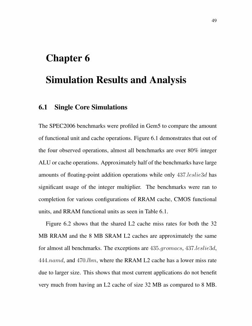
Chapter 6
Simulation Results and Analysis
6.1 Single Core Simulations
The SPEC2006 benchmarks were profiled in Gem5 to compare the amount
of functional unit and cache operations. Figure 6.1 demonstrates that out of
the four observed operations, almost all benchmarks are over 80% integer
ALU or cache operations. Approximately half of the benchmarks have large
amounts of floating-point addition operations while only 437.leslie3d has
significant usage of the integer multiplier. The benchmarks were ran to
completion for various configurations of RRAM cache, CMOS functional
units, and RRAM functional units as seen in Table 6.1.
Figure 6.2 shows that the shared L2 cache miss rates for both the 32
MB RRAM and the 8 MB SRAM L2 caches are approximately the same
for almost all benchmarks. The exceptions are 435.gromacs, 437.leslie3d,
444.namd, and 470.lbm, where the RRAM L2 cache has a lower miss rate
due to larger size. This shows that most current applications do not benefit
very much from having an L2 cache of size 32 MB as compared to 8 MB.

50
401.bzip2
416.gamess
429.mcf
433.milc
435.gromacs
437.leslie
3d
444.namd
445.gobmk
450.soplex
453.povray
454.calcu
lix
458.sjeng
459.GemsFDTD
462.libquantum
464.h264ref
470.lbm
471.omnetpp
998.specra
nd_i
999.specra
nd_f0
20
40
60
80
% o
f Tota
l O
pera
tions
38.1604 40.3841 37.9409 50.5025 49.9734 45.0746 42.5834 35.1056 38.9890 52.4681 33.4019 41.7189 36.6761 31.0232 45.4966 47.6588 47.9110 44.6939 44.6939
61.8395 51.1454 62.0478 33.2294 31.7969 38.0729 34.0415 64.7727 55.9571 39.9750 63.9924 58.0799 55.1224 68.7763 53.8711 16.3716 50.6027 54.4946 54.4946
ALU OpsCache Ops
92
94
96
98
100
% o
f Tota
l O
pera
tions
(Zoom
)
0.0001 0.2708 0.0114 0.1602 0.0700 9.0017 0.0170 0.0768 0.0507 0.0155 0.1377 0.0405 0.9060 0.0002 0.4215 0.0125 0.0457 0.6154 0.6154
0.0000 8.1997 0.0000 16.1078 18.1597 7.8508 23.3581 0.0450 5.0032 7.5413 2.4681 0.1606 7.2954 0.2003 0.2108 35.9571 1.4406 0.1962 0.1962
SPEC 2006 Benchmark Profiles
FPU OpsMult Ops
Figure 6.1: SPEC2006 Benchmark Profiles
Even though the L2 cache capacity is four times larger for the RRAM L2
cache architecture, there are still approximately the same amount of miss in-
duced writes for most applications. The higher write energy and also larger
capacity of RRAM cache causes twice the amount of energy to be used for
32 MB of RRAM cache than a standard 8 MB SRAM cache.
The architecture having a shared 32 MB RRAM L3 cache with a shared
8 MB SRAM L2 cache uses energy in direct relation to the SRAM L2 cache
miss rate. Benchmarks that have SRAM L2 cache miss rates approaching a
51
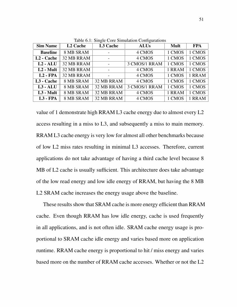
Table 6.1: Single Core Simulation ConfigurationsSim Name L2 Cache L3 Cache ALUs Mult FPA
Baseline 8 MB SRAM - 4 CMOS 1 CMOS 1 CMOSL2 - Cache 32 MB RRAM - 4 CMOS 1 CMOS 1 CMOS
L2 - ALU 32 MB RRAM - 3 CMOS/1 RRAM 1 CMOS 1 CMOSL2 - Mult 32 MB RRAM - 4 CMOS 1 RRAM 1 CMOSL2 - FPA 32 MB RRAM - 4 CMOS 1 CMOS 1 RRAM
L3 - Cache 8 MB SRAM 32 MB RRAM 4 CMOS 1 CMOS 1 CMOSL3 - ALU 8 MB SRAM 32 MB RRAM 3 CMOS/1 RRAM 1 CMOS 1 CMOSL3 - Mult 8 MB SRAM 32 MB RRAM 4 CMOS 1 RRAM 1 CMOSL3 - FPA 8 MB SRAM 32 MB RRAM 4 CMOS 1 CMOS 1 RRAM
value of 1 demonstrate high RRAM L3 cache energy due to almost every L2
access resulting in a miss to L3, and subsequently a miss to main memory.
RRAM L3 cache energy is very low for almost all other benchmarks because
of low L2 miss rates resulting in minimal L3 accesses. Therefore, current
applications do not take advantage of having a third cache level because 8
MB of L2 cache is usually sufficient. This architecture does take advantage
of the low read energy and low idle energy of RRAM, but having the 8 MB
L2 SRAM cache increases the energy usage above the baseline.
These results show that SRAM cache is more energy efficient than RRAM
cache. Even though RRAM has low idle energy, cache is used frequently
in all applications, and is not often idle. SRAM cache energy usage is pro-
portional to SRAM cache idle energy and varies based more on application
runtime. RRAM cache energy is proportional to hit / miss energy and varies
based more on the number of RRAM cache accesses. Whether or not the L2

52
401.bzip2
416.gamess
429.mcf
433.milc
435.gromacs
437.leslie
3d
444.namd
445.gobmk
450.soplex
453.povray
454.calcu
lix
458.sjeng
459.GemsFDTD
462.libquantum
464.h264ref
470.lbm
471.omnetpp
998.specra
nd_i
999.specra
nd_f0.0
0.5
1.0
1.5
2.0
2.5
3.0
3.5
Norm
aliz
ed E
nerg
y
Normalized Energy for 32MB L2 RRAM Cache and 32MB L3 RRAM Cache
8MB L2 SRAM32MB L2 RRAM8MB L2 SRAM32MB L3 RRAM
0.0
0.2
0.4
0.6
0.8
1.0
1.2
Mis
s R
ate
8MB L2 SRAM Miss Rate32MB L2 RRAM Miss Rate
Figure 6.2: SPEC2006 Benchmark Energy Usage for Different Cache Levels
RRAM architecture or the L3 RRAM architecture is more energy efficient
is dependant on the application being run. 68% of the SPEC 2006 bench-
marks have better cache energy efficiency using the L3 RRAM architecture,
while the other 32% have better cache energy efficiency for the L2 RRAM
architecture.
As stated previously, most benchmarks do not benefit from having an L2
cache of size 32 MB as compared to 8 MB for the L2 RRAM architecture.
Out of the four exceptions, two benchmarks saw a slight speedup of up

53
to 1.06 (437.leslie3d and 470.lbm) due to a decrease in miss rates when
having the larger 32 MB RRAM L2 cache as seen in Figures 6.2 and 6.3.
The reason more speedup is not seen is because of the slightly slower read
latency of RRAM cache compared to SRAM cache. This reinforces the
statement that most current applications do not benefit from having a larger
than 8 MB L2 cache, but overall, the system performance is not negatively
affected.
401.bzip2
416.gamess
429.mcf
433.milc
435.gromacs
437.leslie
3d
444.namd
445.gobmk
450.soplex
453.povray
454.calcu
lix
458.sjeng
459.GemsFDTD
462.libquantum
464.h264ref
470.lbm
471.omnetpp
998.specra
nd_i
999.specra
nd_f0.0
0.2
0.4
0.6
0.8
1.0
1.2
Norm
aliz
ed R
unti
me
Normalized Runtime for 32MB L2 RRAM Cache and 32MB L3 RRAM Cache
8MB L2 SRAM32MB L2 RRAM32MB L3 RRAM
Figure 6.3: SPEC2006 Benchmark Timing for Different Cache Levels
The RRAM L3 cache architecture also demonstrated similar speedup for

54
the same two benchmarks, but saw slight performance degradation in three
additional benchmarks. These slowdowns are due to accesses to main mem-
ory having to miss through three levels of cache, and can be seen for bench-
marks 429.mcf , 445.gobmk and 458.GemsFDTD. This demonstrates that
having three levels of cache does not improve the performance of current ap-
plications. Based on the cache access patterns, a third cache level can even
hinder performance.
These results show that the RRAM L2 cache architecture performs ap-
proximately the same as or better than the RRAM L3 cache architecture for
all cases. When taking into account both energy efficiency and performance
of RRAM cache, the RRAM L2 cache architecture remains sufficient, al-
though the RRAM L3 cache architecture can be more energy efficient.
Figures 6.4 and 6.5 show the performance of the SPEC 2006 benchmarks
with CMOS functional units replaced in the RRAM layer. The graphs for
both architectures are nearly identical because RRAM access time for func-
tional unit operations is not dependent on the level at which the RRAM is
used for cache.
Having an ALU implemented in RRAM reduces the completion time of
all benchmarks by ∼77% on average. This slowdown occurs due to fac-
tors including the slower speed of the RRAM ALU, and also the depen-
dencies that occur between ALU operations. Since almost all benchmarks

55
have a high percentage of ALU operations, they generally have more depen-
dencies between instructions involving operands that are calculated using
ALUs. This causes the remaining faster CMOS ALUs to stall, waiting for
the RRAM ALU to achieve a result they require.
401.bzip2
416.gamess
429.mcf
433.milc
435.gromacs
437.leslie
3d
444.namd
445.gobmk
450.soplex
453.povray
454.calcu
lix
458.sjeng
459.GemsFDTD
462.libquantum
464.h264ref
470.lbm
471.omnetpp
998.specra
nd_i
999.specra
nd_f0.0
0.5
1.0
1.5
2.0
2.5
3.0
3.5
Norm
aliz
ed R
unti
me
Normalized Runtime for 32MB L2 RRAM LUT-based FUs
All CMOS FUsRRAM ALURRAM Mult.RRAM FPU
Figure 6.4: SPEC2006 Benchmark Runtime With L2 RRAM Cache and Replaced LUT-Based FUs
Benchmarks involving low percentages of integer multiplier operations
and floating-point adder (FPA) operations show very minimal reduction in

56
performance, such as 401.bzip2, 445.gobmk and 462.libquantum. Con-
versely, benchmarks involving high percentages of integer multiplier opera-
tions and FPA operations show high performance degradation. Worst cases
show that 437.leslie3d completes 126% slower for a replaced integer mul-
tiplier, and 444.namd completes 225% slower for a replaced FPA.
401.bzip2
416.gamess
429.mcf
433.milc
435.gromacs
437.leslie
3d
444.namd
445.gobmk
450.soplex
453.povray
454.calcu
lix
458.sjeng
459.GemsFDTD
462.libquantum
464.h264ref
470.lbm
471.omnetpp
998.specra
nd_i
999.specra
nd_f0.0
0.5
1.0
1.5
2.0
2.5
3.0
3.5
Norm
aliz
ed R
unti
me
Normalized Runtime for 32MB L3 RRAM LUT-based FUs
All CMOS FUsRRAM ALURRAM Mult.RRAM FPU
Figure 6.5: SPEC2006 Benchmark Runtime With L3 RRAM Cache and Replaced LUT-Based FUs
The energy usage of CMOS functional units and RRAM functional units
for the SPEC 2006 benchmarks is shown in Figure 6.6 for the RRAM L2
cache architecture and Figure 6.7 for the RRAM L3 cache architecture.

57
Again, the graphs for both architectures are nearly identical because the
RRAM functional unit operate independent of the level at which the RRAM
is used for cache. Few small variations are due to idle energy between the
slightly different runtimes.
401.bzip2
416.gamess
429.mcf
433.milc
435.gromacs
437.leslie
3d
444.namd
445.gobmk
450.soplex
453.povray
454.calcu
lix
458.sjeng
459.GemsFDTD
462.libquantum
464.h264ref
470.lbm
471.omnetpp
998.specra
nd_i
999.specra
nd_f0
1
2
3
4
5
6
7
Norm
aliz
ed E
nerg
y
Normalized Energy for 32MB L2 RRAM LUT-based FUs
All CMOS FUsRRAM ALURRAM Mult.RRAM FPU
Figure 6.6: SPEC2006 Benchmark Energy With L2 RRAM Cache and Replaced LUT-Based FUs
The RRAM functional unit energy usage is normalized to the strictly
CMOS functional unit energy usage. Therefore, the failed CMOS ALU /
one RRAM ALU value is the total energy of all four ALU functional units
(three CMOS and one RRAM). It can be seen that benchmarks require three

58
to five times more energy on average when using an RRAM ALU. This can
be attributed to both the additional idle energy from the three CMOS ALUs
due to increased runtime, and the access energy of the RRAM ALU due to
frequency of use, as all benchmarks perform a significant number of ALU
operations.
401.bzip2
416.gamess
429.mcf
433.milc
435.gromacs
437.leslie
3d
444.namd
445.gobmk
450.soplex
453.povray
454.calcu
lix
458.sjeng
459.GemsFDTD
462.libquantum
464.h264ref
470.lbm
471.omnetpp
998.specra
nd_i
999.specra
nd_f0
1
2
3
4
5
6
7
Norm
aliz
ed E
nerg
y
Normalized Energy for 32MB L3 RRAM LUT-based FUs
All CMOS FUsRRAM ALURRAM Mult.RRAM FPU
Figure 6.7: SPEC2006 Benchmark Energy With L3 RRAM Cache and Replaced LUT-Based FUs
When the CMOS integer multiplier is replaced in RRAM, energy usage
is reduced for all benchmarks except 437.leslie3d. This can be attributed to
the large percentage of integer multiplication operations for that benchmark,

59
and the number of arrays accessed for one computation. The reduction in
energy usage for integer multiplication for all other benchmarks is due to the
low idle energy of RRAM and minimal number of operations performed.
The same sentiments can be said for the floating-point adder in RRAM.
Benchmarks with higher percentages of FPA operations, over 3%, show
increased energy usage when compared to the CMOS FPA. For benchmarks
where the FPA is not used frequently, the RRAM implementation improves
energy efficiency.
The FIT rate decreases, and therefore reliability increases, for both the
RRAM L2 cache architecture and RRAM L3 cache architecture in this re-
search because hard errors occurring in CMOS functional units are miti-
gated by implementing replacements in the RRAM layer, preventing system
failure. The RRAM L2 cache architecture’s performance is better for all of
the benchmarks compared to the RRAM L3 cache architecture, indepen-
dent of the number of functional units implemented, while the RRAM L3
cache architecture’s energy efficiency is better for 68% of the benchmarks.
Overall benchmark performance and energy efficiency when CMOS units
are replaced in the RRAM layer depends on the benchmark instruction pro-
file, which is application dependent, and architecture independent. Using
an RRAM L2 cache is sufficient compared to using an RRAM L3 cache
because both architectures improve reliability and the difference in efficacy

60
between them is negligible.
6.2 Multi-core Simulations
blackscholes
bodytrack
canneal
facesim ferret
fluidanim
ate vips0
10
20
30
40
50
60
70
% o
f Tota
l O
pera
tions
45.3873 37.3722 35.1206 54.2564 36.4885 41.2229 32.3283
45.9803 40.3718 51.5523 23.9498 54.7293 47.8676 59.6228
ALU OpsCache Ops
80
85
90
95
100
% o
f Tota
l O
pera
tions
(Zoom
)
0.0004 2.4705 0.0042 0.0092 0.1457 0.0921 1.7631
8.6320 19.7855 13.3229 21.7846 8.6365 10.8174 6.2857
PARSEC Benchmark Profiles
FPU OpsMult Ops
Figure 6.8: SPEC2006 Benchmark Energy With L3 RRAM Cache and Replaced LUT-Based FUs
The PARSEC benchmarks were profiled in Gem5 to compare the amount
of functional unit and cache operations. Figure 6.8 demonstrates that out of
the four observed operations, all benchmarks are over 75% integer ALU or

61
cache operations. All benchmarks have large amounts of floating-point ad-
dition operations while no benchmark has significant usage of the integer
multiplier. The benchmarks were ran to completion for various configura-
tions of RRAM cache, CMOS functional units, and RRAM functional units
as seen in Table 6.2.
Table 6.2: Multi-Core Simulation Configurations
Sim Name L2 Cache # Cores, ALUs # Cores, Mult # Cores, FPA8 Core Default 64 MB SRAM All, 4 CMOS All, 1 CMOS All, 1 CMOS8 Core RRAM 256 MB RRAM Default Default Default
8 Core ALU 256 MB RRAM 1, 3 CMOS/1 RRAM Default Default8 Core Mult 256 MB RRAM Default 1, 1 RRAM Default8 Core FPA 256 MB RRAM Default Default 1, 1 RRAM
8 Core ALU4 256 MB RRAM 4, 3 CMOS/1 RRAM Default Default8 Core Mult4 256 MB RRAM Default 4, 1 RRAM Default8 Core FPA4 256 MB RRAM Default Default 4, 1 RRAM
16 Core Default 128 MB SRAM Default Default Default16 Core RRAM 512 MB RRAM Default Default Default
16 Core ALU 512 MB RRAM 1, 3 CMOS/1 RRAM Default Default16 Core Mult 512 MB RRAM Default 1, 1 RRAM Default16 Core FPA 512 MB RRAM Default Default 1, 1 RRAM
16 Core ALU8 512 MB RRAM 8, 3 CMOS/1 RRAM Default Default16 Core Mult8 512 MB RRAM Default 8, 1 RRAM Default16 Core FPA8 512 MB RRAM Default Default 8, 1 RRAM
Note: Cores not mentioned have the default # of CMOS units and 0 RRAM units
As seen in Figure 6.9, very few benchmarks had a speedup with the larger
RRAM L2 cache size, with exceptions being ferret and vips for the 8-
core architectures. Every other benchmark, when having a large RRAM L2
cache, did not show much performance change at all. Again, this shows that
most current applications do not benefit, or get degraded, by having a very

62
large L2 cache. Generally, default cache sizes are sufficient, but having a
larger L2 cache can improve performance in some cases by not having to
overwrite data as often as a smaller cache size would.
blackscholes
bodytrack
canneal
facesim ferret
fluidanim
ate vips0.0
0.2
0.4
0.6
0.8
1.0
1.2
1.4
Norm
aliz
ed R
unti
me
Normalized Runtime for L2 SRAM and L2 RRAM Caches
64MB L2 SRAM 8-Cores256MB L2 RRAM 8-Cores128MB L2 SRAM 16-Cores512MB L2 RRAM 16-Cores
Figure 6.9: PARSEC Benchmark Runtime for L2 SRAM and L2 RRAM Caches
As expected, mosts benchmarks showed improvement from the 8-core
to the 16-core architectures due to less word being performed per core in
parallel. Benchmarks fluidanimate and vips had some slight degradation
of performance when using 16-cores due to the increased communication
between cores. Inter-dependant workloads were spread across too many

63
cores, and therefore, time was spent waiting for results from other cores
rather than performing computation. Some slowdown was experienced by
these benchmarks as well, which can be attributed to the higher latency of
RRAM cache over SRAM cache.
blackscholes
bodytrack
canneal
facesim ferret
fluidanim
ate vips0
1
2
3
4
5
6
Norm
aliz
ed E
nerg
y
Normalized Energy for L2 SRAM and L2 RRAM Caches
64MB L2 SRAM 8-Cores256MB L2 RRAM 8-Cores128MB L2 SRAM 16-Cores512MB L2 RRAM 16-Cores
Figure 6.10: PARSEC Benchmark Energy for L2 SRAM and L2 RRAM Caches
As seen in Figure 6.10, more energy is used by the SRAM cache in the
16-core architecture compared to the 8-core architecture, due to the larger
capacity and increased cross-core communication through the shared L2
cache. Corresponding RRAM L2 cache architectures use approximately
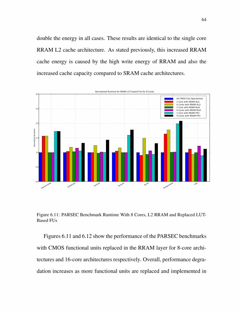
64
double the energy in all cases. These results are identical to the single core
RRAM L2 cache architecture. As stated previously, this increased RRAM
cache energy is caused by the high write energy of RRAM and also the
increased cache capacity compared to SRAM cache architectures.
blackscholes
bodytrack
canneal
facesim ferret
fluidanim
ate vips0.0
0.5
1.0
1.5
2.0
2.5
3.0
Norm
aliz
ed R
unti
me
Normalized Runtime for RRAM LUT-based FUs for 8-Cores
All CMOS FUs Operational
1 Core with RRAM ALU4 Cores with RRAM ALU1 Core with RRAM Mult4 Cores with RRAM Mult1 Core with RRAM FPU4 Cores with RRAM FPU
Figure 6.11: PARSEC Benchmark Runtime With 8 Cores, L2 RRAM and Replaced LUT-Based FUs
Figures 6.11 and 6.12 show the performance of the PARSEC benchmarks
with CMOS functional units replaced in the RRAM layer for 8-core archi-
tectures and 16-core architectures respectively. Overall, performance degra-
dation increases as more functional units are replaced and implemented in

65
the RRAM layer. One core with a failed CMOS functional unit implemented
in the RRAM slows the performance of the system down less than if half the
cores have the same unit failed. The amount of degradation for a specific
functional unit is dependent on the application profile of the benchmark,
specifically the frequency of usage of that functional unit. Benchmarks with
high usage of a failed unit will have a greater slowdown due to the imple-
mented unit in RRAM being slower, creating a bottleneck for that core.
blackscholes
bodytrack
canneal
facesim ferret
fluidanim
ate vips0.0
0.5
1.0
1.5
2.0
2.5
3.0
Norm
aliz
ed R
unti
me
Normalized Runtime for RRAM LUT-based FUs for 16-Cores
All CMOS FUs Operational
1 Core with RRAM ALU8 Cores with RRAM ALU1 Core with RRAM Mult8 Cores with RRAM Mult1 Core with RRAM FPU8 Cores with RRAM FPU
Figure 6.12: PARSEC Benchmark Runtime With 16 Cores, L2 RRAM and Replaced LUT-Based FUs
In general, the 16-core architecture has less performance degradation
66
than the 8-core architecture, and both architectures perform better than the
single-core architecture with RRAM L2 cache. All three architectures can
be compared because the SPEC 2006 benchmarks profiles are similar to the
PARSEC benchmark profiles. This degradation decrease can be attributed to
the fact that the work is spread out across more cores, meaning there are ad-
ditional CMOS units available as the number of cores increases, which are
faster than units implemented in RRAM. The average runtime of a single-
core system with RRAM L2 cache was between∼1.5 and∼2.5 times longer
than the baseline system, while the average runtime of an 8-core system was
between ∼1.25 and ∼2 times longer than the baseline system and the aver-
age runtime of a 16-core system was between ∼1.2 and ∼1.5 times longer.
The energy usage of CMOS functional units and RRAM functional units
for the PARSEC benchmarks is show in Figure 6.13 for the 8-core archi-
tectures and Figure 6.14 for the 16-core architectures. These two graphs
are very similar despite the performance degradation being worse for the
8-core architectures. This is caused by the two architectures having equal
ratios of CMOS to RRAM functional units. It can also be seen that, again,
the energy usage is dependent on functional unit usage. Most benchmarks
have high energy usage for RRAM implemented ALUs and floating-point
adders because the benchmarks perform a large number of operations using
those functional units. The increased amount of energy is partially due to

67
blackscholes
bodytrack
canneal
facesim ferret
fluidanim
ate vips0.0
0.5
1.0
1.5
2.0
2.5
3.0
3.5
4.0
Norm
aliz
ed E
nerg
y
Normalized Energy for RRAM LUT-based FUs for 8-Cores
All CMOS FUs Operational
1 Core with RRAM ALU4 Cores with RRAM ALU1 Core with RRAM Mult4 Cores with RRAM Mult1 Core with RRAM FPU4 Cores with RRAM FPU
Figure 6.13: PARSEC Benchmark Energy With 8 Cores, L2 RRAM and Replaced LUT-Based FUs
idle energy due to increased runtime, and also the number of RRAM arrays
used for functional unit implementation. Energy usage for the multiplica-
tion units is less than the baseline in most benchmarks due to the lack of
multiplication operations in the benchmarks. The more CMOS multipliers
are replaced in the RRAM layer, the less total energy is used by multiplica-
tion units overall because RRAM has lower idle energy than CMOS.
Since performance degradation decreases with more cores, the increase

68
blackscholes
bodytrack
canneal
facesim ferret
fluidanim
ate vips0.0
0.5
1.0
1.5
2.0
2.5
3.0
3.5
4.0
Norm
aliz
ed E
nerg
y
Normalized Energy for RRAM LUT-based FUs for 16-Cores
All CMOS FUs Operational
1 Core with RRAM ALU8 Cores with RRAM ALU1 Core with RRAM Mult8 Cores with RRAM Mult1 Core with RRAM FPU8 Cores with RRAM FPU
Figure 6.14: PARSEC Benchmark Energy With 16 Cores, L2 RRAM and Replaced LUT-Based FUs
of functional unit energy consumption due to idle energy was not as signifi-
cant as it was for a single-core system. Overall, the amount of energy con-
sumption increased less for multi-core systems as compared to single-core
systems. The average energy consumption for the ALU and floating-point
adder operations for single-core systems using RRAM functional units was
between ∼2 and ∼5 times more than the baseline, while the average energy
usage for multi-core systems using RRAM functional units was between

69
∼1.25 and ∼2.75 times more. The FIT rate decreases, and therefore relia-
bility increases, for both the 8-core and 16-core architecture in this research
because hard errors occurring in CMOS functional units are mitigated by
implementing replacements in the RRAM layer, preventing system failure.
Overall, using RRAM for cache can speed up a system, regardless of
what level of cache it is implemented as. Using RRAM for functional
unit implementation, replacing CMOS functional units that have failed, en-
hances the reliability of a system, at the cost of performance degradation and
increased energy usage for frequently used functional units. Sparsely used
functional units implemented in RRAM use less energy overall due to the
low idle energy of RRAM. The magnitude of degradation and energy usage
is dependent on the application profile, and not the level at which RRAM is
used for cache.

70
Chapter 7
Conclusions
This research demonstrated that total system failure can be mitigated by dy-
namically reconfiguring a portion of RRAM cache to implement a failed
CMOS functional unit, increasing the reliability of a system. The proposed
architecture was validated using the Gem5 performance simulator and the
McPAT simulator, running SPEC 2006 and PARSEC benchmarks. The
benchmarks successfully completed with functional units implemented as
LUT-based RRAM logic units. The large size of the RRAM cache com-
pared to traditional CMOS cache allows for larger subspaces to be imple-
mented in RRAM without reducing the cache hit rate. Best case perfor-
mance speedup was as high 1.25 with the use of a large capacity RRAM
cache without logic implementation, while the best case RRAM functional
unit energy consumption was below 10% of the CMOS energy consumption
for the RRAM multiplier and floating-point adder.
The average runtime when using RRAM for functional unit replacement

71
was between ∼1.5 and ∼2.5 times longer than the baseline for a single-
core architecture,∼1.25 and∼2 times longer for an 8-core architecture, and
∼1.2 and∼1.5 times longer for a 16-core architecture. Average energy con-
sumption when using RRAM for functional unit replacement was between
∼2 and ∼5 times more than the baseline for a single-core architecture, and
∼1.25 and ∼2.75 times more for multi-core architectures. Performance
degradation was caused by slower than CMOS access time of RRAM, the
number of sequential RRAM reads required to perform an operation, and
the instruction profile of a benchmark. Energy consumption increase was
due to additional idle energy used during extended runtime of a benchmark
and the number of arrays required to perform an operation in RRAM. The
performance degradation and energy consumption increase is justified by
the prevention of system failure and enhanced reliability.
Overall, the proposed architecture shows promise for use in multi-core
systems. Average performance degradation decreases as more cores are
used due to more total functional units being available, preventing a slow
RRAM functional unit from becoming a bottleneck. This research has also
created a framework for testing hybrid CMOS/RRAM architectures, with
which future realizations of RRAM can be implemented and compared. As
new materials for RRAM are used, improved performance and energy effi-
ciency will demonstrate better results.

72
Chapter 8
Future Work
As previous research has shown, RRAM can be used for temperature sens-
ing [30]. Hybrid CMOS/RRAM architectures implemented as 3D-ICs can
passively sense temperature of the CMOS layer while performing cache op-
erations, or actively sense temperature by accessing a specific RRAM loca-
tion. If dangerously high temperatures are detected in a CMOS functional
unit, the system could temporarily deactivate the component and migrate
activity to the functional unit implemented in RRAM temporarily. This
would degrade system performance during the time which operations are
performed in the RRAM layer, but it allows the CMOS functional unit to
cool, preventing permanent damage.
Another application that could be researched in the future as improved re-
alizations of RRAM are implemented is hardware acceleration. An applica-
tion’s runtime profile could be analyzed before or during runtime and addi-
tional functional units could be implemented in the RRAM layer as needed.

73
If a large number of independent multiplications are required, such as ma-
trix multiplication, additional multipliers could be implemented in RRAM
layer to parallelize the computation and speedup the overall application.

74
Bibliography
[1] Itrs 2011 executive summary, 2011.
[2] Sobeeh Almukhaizim and Ozgur Sinanoglu. Novel hazard-free ma-jority voter for n-modular redundancy-based fault tolerance in asyn-chronous circuits. IET Computers Amp; Digital Techniques, pages306–315, 2011.
[3] K. Amanuma, T. Tatsumi, Y. Maejima, S. Takahashi, H. Hada, H. Ok-izaki, and T. Kunio. Capacitor-on-metal/via-stacked-plug (cmvp)memory cell for 0.25um cmos embedded feram. In Electron Devices
Meeting, 1998. IEDM ’98 Technical Digest., International, pages 363–366, Dec 1998.
[4] Yi-Ching (Jean) Wu Tzu-Ning Fang Zhida Lan Steven AvanzinoSuzette Pangrle Matthew Buynoski Manuj Rathor Wei (Daisy) CaiNick Tripsas Colin Bill Michael VanBuskirk An Chen, Sameer Had-dad and Masao Taguchi. Non-volatile resistive switching for advancedmemory applications. IEEE, 2005.
[5] IEEE Computer Society Authors. Ieee standard for floating-point arith-metic. IEEE Std 754-2008, pages 1–58, 29 2008.
[6] Christian Bienia, Sanjeev Kumar, Jaswinder Pal Singh, and Kai Li.The parsec benchmark suite: Characterization and architectural impli-cations. Princeton University Technical Report, 2008.

75
[7] Nathan Binkert, Bradford Beckmann, Gabriel Black, Steven K. Rein-hardt, Ali Saidi, Arkaprava Basu, Joel Hestness, Derek R. Hower,Tushar Krishna, Somayeh Sardashti, Rathijit Sen, Korey Sewell,Muhammad Shoaib, Nilay Vaish, Mark D. Hill, and David A. Wood.The gem5 simulator. SIGARCH Comput. Archit. News, 39:1–7, 2011.
[8] C. F. Chen, C. T. Chen, J. Y. Yu, S. Wu, S. L. Lung, and R. Liu.An access-transistor-free (0t/1r) non-volatile resistance random ac-cess memory (rram) using a novel threshold switching, self-rectifyingchalcogenide device. IEEE International Electron Devices Meeting
2003, pages 37.4.1–37.4.4, 2003.
[9] Kwang-Ting Tim Cheng and Dmitri B. Strukov. 3d cmos-memristorhybrid circuits: Devices, integration, architecture, and applications. InProceedings of the 2012 ACM International Symposium on Physical
Design, ISPD ’12, pages 33–40. ACM, 2012.
[10] L.O. Chua and Purdue University. School of Electrical Engineering.Memristor: The Missing Circuit Element. TR-EE. School of ElectricalEngineering, Purdue University, 1970.
[11] David W. Coit. Cold-standby redundancy optimization for nonre-pairable systems. IIE Transactions, 33:471–478, 2001.
[12] Compaq Computer Corporation. Alpha 21264 microprocessor hard-ware reference manual.
[13] Standard Performance Evaluation Corporation. Spec cpu2006 bench-mark descriptions. SIGARCH Computer Architecture News, 35:84–89,March 2007.
[14] P. T. De Sousa and F. P. Mathur. Sift-out modular redundancy. IEEE
Trans. Comput., 27:624–627, 1978.

76
[15] Xiangyu Dong, Xiaoxia Wu, Guangyu Sun, Yuan Xie, H. Li, and YiranChen. Circuit and microarchitecture evaluation of 3d stacking mag-netic ram (mram) as a universal memory replacement. In Design Au-
tomation Conference, 2008. DAC 2008. 45th ACM/IEEE, pages 554–559, june 2008.
[16] Mark Gebhart, Joel Hestness, Ehsan Fatehi, Paul Gratz, andStephen W. Keckler. Running parsec 2.1 on m5. Technical Report.
[17] Sieu D. Ha and Shriram Ramanathan. Adaptive oxide electronics: Areview. Journal of Applied Physics, 110, 2011.
[18] John Hennessy and David Patterson. Computer Architecture - A Quan-
titative Approach. Morgan Kaufmann, 2003.
[19] John L. Henning. Spec cpu2006 memory footprint. SIGARCH Com-
puter Architecture News, 35:84–89, March 2007.
[20] Y.N. Hwang, J.S. Hong, S.H. Lee, S.J. Ahn, G.T. Jeong, G.H. Koh, J.H.Oh, H.J. Kim, W.C. Jeong, S.Y. Lee, J.H. Park, K.C. Ryoo, H. Horii,Y.H. Ha, J.H. Yi, W.Y. Cho, Y.T. Kim, K.H. Lee, S.H. Joo, S.O. Park,U.I. Chung, H.S. Jeong, and Kinam Kim. Full integration and reli-ability evaluation of phase-change ram based on 0.24um cmos rech-nologies. In VLSI Technology, 2003. Digest of Technical Papers. 2003
Symposium on, pages 173–174, June 2003.
[21] Engin Ipek, Xiaochen Guo, and Tolga Soyata. Resistive computation:Avoiding the power wall with low-leakage, stt-mram based computing.June 2010.
[22] Sung Hyun Jo and Wei Lu. Cmos compatible nanoscale nonvolatileresistance switching memory, 2007.

77
[23] A. H. Johnston, G. M. Swift, and D.C. Shaw. Impact of cmos scalingon single-event hard errors in space systems, 1995.
[24] C.-M. Jung, J.-M. Choi, and K.-S. Min. Two-step write scheme forreducing sneak-path leakage in complementary memristor array. Nan-
otechnology, IEEE Transactions on, pages 611–618, 2012.
[25] D. Lee, S. Baek, M. Ree, and O. Kim. Unipolar resistive switch-ing characteristic of semiconducting poly film. Electronics Letters,44(9):596–597, 24 2008.
[26] Sheng Li, Jung Ho Ahn, Richard D. Strong, Jay B. Brockman, Dean M.Tullsen, and Norman P. Jouppi. Mcpat: An integrated power, area, andtiming modeling framework for multicore and manycore architectures.In Proceedings of the 42nd Annual IEEE/ACM International Sympo-
sium on Microarchitecture, MICRO 42, pages 469–480. ACM, 2009.
[27] Loucas Louca, Todd A. Cook, and William H. Johnson. Implementa-tion of ieee single precision floating-point addition and multiplicationon fpgas. IEEE, pages 107–116, 1996.
[28] Wei Lu, Kuk-Hwan Kim, Siddharth Gaba, Dana Wheeler, Jose Cruz-Albrecht, Tahir Hussain, and Narayan Srinivasa. A functional hybridmemristor crossbar-array/cmos system for data storage and neuromor-phic applications. Nano Letters, 2011.
[29] Harika Manem and Garrett S. Rose. A read-monitored write circuit for1t1m multi-level memristor memories. pages 2938–2941. IEEE, 2011.
[30] Cory E. Merkel. Thermal profiling in cmos/memristor hybrid architec-tures. 2011.

78
[31] Cory E. Merkel, Nakul Nagpal, Sindhura Mandalapu, and DhireeshaKudithipudi. Reconfigurable n-level memristor memory design. InIJCNN, pages 3042–3048, 2011.
[32] Shubhendu S. Mukherjee, Peter Bannon, Steven Lang, Aaron Spink,and David Webb. The alpha 21364 network architecture. In Proceed-
ings of the The Ninth Symposium on High Performance Interconnects,HOTI ’01, page 113. IEEE Computer Society, 2001.
[33] Agner Fog. Copenhagen University College of Engineering. Instruc-tion tables: Lists of instruction latencies, throughputs, and micro-operation breakdowns.
[34] Somnath Paul and Swarup Bhunia. Dynamic transfer of computationto processor cache for yield and reliability improvement. IEEE Trans.
VLSI Syst., 19:1368–1379, 2011.
[35] R. Rosezin, E. Linn, L. Nielen, C. Ku andgeler, R. Bruchhaus, andR. Waser. Integrated complementary resistive switches for passivehigh-density nanocrossbar arrays. Electron Device Letters, IEEE,32(2):191–193, Feb 2011.
[36] C. Senthilpari, G. Ramanamurthy, and P. Velrajkumar. An efficient epiand energy consumption of 32 bit alu using shannon theorem basedadder approach. volume 10, pages 231–238, July 2011.
[37] Jayanth Srinivasan, Sarita V. Adve, Pradip Bose, and Jude Rivers. Thecase for lifetime reliability-aware microprocessors, 2004.
[38] Jayanth Srinivasan, Sarita V. Adve, Pradip Bose, and Jude A. Rivers.The impact of technology scaling on lifetime reliability. In Proceed-
ings of the 2004 International Conference on Dependable Systems and
Networks, DSN ’04, page 177. IEEE Computer Society, 2004.

79
[39] Dmitri B. Strukov, Gregory S. Snider, Duncan R. Stewart, and R. Stan-ley Williams. The missing memristor found. Nature, 453:80–83, 2008.
[40] John von Neumann. Probabilistic logics and the synthesis of reliableorganisms from unreliable components. Automata Studies, pages 43–98, 1956.
[41] W. Wang, M. Liu, D. Strukov, and G.S. Rose. Hybrid
CMOS/Memristor Nanoelectronics. Springer, 2011.
[42] Qiangfei Xia, Warren Robinett, Michael W. Cumbie, Neel Baner-jee, Thomas J. Carinali, J. Joshua Yang, Wei Wu, Xuema Li,William M. Tong, Dmitri B. Strukov, Gergory S. Snider, Medeiros-Ribeiro Gilberto, and R. Stanley Williams. Memristor-cmos hybridintegrated circuits for reconfigurable logic. American Chemical Soci-
ety, 2009.
[43] Cong Xu, Xiangyu Dong, Norman P. Jouppi, and Yuan Xie. Designimplications of memristor-based rram cross-point structures. pages734–739. IEEE, 2011.
[44] Mahmut Yilmaz, Albert Meixner, Sule Ozev, and Daniel J. Sorin. Lazyerror detection for microprocessor functional units. In In Proc. of the
IEEE Intl Symp. on Defect and Fault Tolerance in VLSI Systems, 2007.
[45] Yeo K. S. Yu H., Zhang W. Design exploration of hybrid cmos andmemristor circuits by new modified nodal analysis. pages 1–15. IEEE,2011.