Reconfigurable Antennas and their Applications Elements UWB-MIMO antenna Dimensions are 23 x 39.8 mm...
41
PhD Candidate: Muhammad Saeed Khan Department of Information Engineering, University of Padova Supervised By: Antonio - Daniele Capobianco Funded By: Cariparo Foundation November, 24, 2015 Reconfigurable Antennas and their Applications
Transcript of Reconfigurable Antennas and their Applications Elements UWB-MIMO antenna Dimensions are 23 x 39.8 mm...

PhD Candidate:
Muhammad Saeed Khan
Department of Information Engineering,
University of Padova
Supervised By: Antonio-Daniele Capobianco
Funded By: Cariparo Foundation
November, 24, 2015
Reconfigurable Antennas
and their Applications

Copyright© The use of this work is restricted solely for academic purposes. The author of this work owns the copyright and no reproduction in any form is permitted without written permission by the authors.

AbstractOne of the biggest challenge in modern communication systems is to provide a single antenna for different applications. Existing antenna systems are limited to some applications. So it is important to design a single reconfigurable antenna for multiple applications.
Five different reconfigurable printed antennas for different applications are designed during the study of this thesis. In the first design an antenna for frequency reconfigurable applications is designed. The electrical length of the conductor is changed using PIN diodes and the resonance of antenna is shifted from 4.27 GHz to 3.56 GHz. Good agreement between simulated and measured results is observed. In the second and third designs, Ultra wideband (UWB) Multiple-Input Multiple-Output (MIMO) antennas with on-demand Wireless Local Area Network (WLAN) rejection are designed. The second design consists of two elements UWB-MIMO antenna and stubs are connected to the ground plane using PIN diodes. These stubs act as a stop-band filter and reject the band at 5.5 GHz center frequency. This design has a compact size of 23 x 39.8 mm2. The third design has almost same features as of second design but it has four elements. These elements are placed orthogonally to each other. The total size of this proposed design is 50 x 39.8 mm2. The ground plane is common and a band-stop design is placed between the ground planes. This band-stop design is connected with the ground plane using PIN diodes. When diodes are biased, the current is travelled to the nearly placed band-stop design and a notch is obtained around 5.5 GHz. In fourth design a reconfigurable array with a sensing circuit is designed. The array consists of four individual reconfigurable patches which are attached to the different conformal surfaces. These patches are reconfigured from 3.15 GHz to 2.43 GHz using PIN diodes. The correct phase at each element is provided using phase shifters. The sensing circuit is designed in such a way that only input voltage is changed to provide the correct phase on the switching frequency. The patterns of the array are recovered on both switching frequencies when array is attached to wedge or cylindrical surface. In the last design a series-fed array is designed. Composite Right/Left Handed Transmission Line (CRLH-TLs) are used instead of traditional meanderline microstrip lines to connect the array elements. These CRLH-TLs provided the zero phase at each connecting element, which resulted in broad side radiation patterns. To reconfigure the antenna to another frequency a small patch and second CRLH-TL is connected between array elements.
Index Terms: Reconfigurable antennas, PIN diodes, Selflex Antennas, CRLH antenna arrays, UWB-MIMO antennas

BiographyMuhammad Saeed Khan in a researcher at ETIC research center and Research affiliate of Department of Information Engineering, University of Padova, Italy. He received his B.Sc. degree in electrical (telecom) engineering from COMSATS Institute of Information Technology, Islamabad, Pakistan, in 2011. Based on his achievement during his B.Sc. degree, he was awarded EMMA WEST Exchange Scholarship for his B.Sc. mobility Program. He received his Ph.D. degree in 2016 from University of Padova, Italy. He was also recipient of a fully funded Ph.D. scholarship from Cariparo Foundation which provides scholarship to top 15 candidates from all over the world. During his Ph.D. he also spent 18 months at North Dakota State University, USA as a visiting scholar. He was Head of Department of Electrical Engineering Department of Riphah International University, Lahore Campus for one year (2015-2016). His current research interests include advanced techniques and technologies for Antenna design for medical applications, Phased array for radar systems, Reconfigurable antennas for advance applications, UWB-MIMO antennas and novel material based antennas. During this short period of time, he is author-coauthor of more than 40 peer-reviewed journal or conference papers.

Outline
Background
Printed Antennas
Reconfigurable Antennas
Previous Work
Conducted Research
Research question
Diode Model in Simulation
Proposed Designs
Conclusion, challenges and Future Directions

Background of Printed Antennas
Advantages of Printed Antennas
light weight
small size
most useful at microwave frequencies (f > 1 GHz)
a wide range of radiation patterns
typical applications are single element and arrays
History of Printed Antennas
Deschamps's in 1953 [1]
detailed by Alexopoulos [2]
work by Munson 1972 [3]

Background of Reconfigurable
Antennas Reconfigurability means changing the fundamental operating
characteristics of an antenna using electrical, mechanical or other means.
First patent reported in 1983 by Schaubert. [4]
In 1999, a multi university program was launched by Defense Advanced
Research Projects Agency (DAPRA) to investigate reconfigurable antennas
and their applications. [5]
A hot topic of interest these days.
Types of Reconfigurable antennas [6]:

Techniques for reconfigurable
operation Electrically reconfigurable antennas
Using RF-MEMS [7]
Using PIN diodes [8]
Using varactors [9]
Optically reconfigurable antennas
Using nonintegrated optical fibers [10]
Using integrated optical fibers [11]
Using integrated LASER diodes [12]
Physically reconfigurable antennas

Some examples of
Reconfigurable Antennas
(a) (b)
(d) (c)
Figure: Source: R. L. Haupt and M. Lanagan, “Reconfigurable Antennas,” IEEE Antennas and Propagation Magazine, Vol. 55, No. 1, February 2013.

A Comparison of Electrical
Properties
Table 1. Source: http://ieeexplore.ieee.org/stamp/stamp.jsp?tp=&arnumber=6178263

Proposed research
RESEARCH QUESTIONS:
How to implement re-configurability to some novel printed
antennas which are not studied before?
and
What are the trade-offs in the designing of such antennaarrays?

Design of Diode Model in
Simulation
Figure: RF PIN diode: (a) Equivalent circuit model for “ON" conguration; (b) Equivalent circuit model for “OFF" conguration; (c) Biasing Network with PIN diode and RF choke model. Parameters are L = 0.5 nH; RF = 0.8 Ω; RR = 1k Ω; CR = 0.01 pF; CB = 45 pF; LC = 200 nH:

Diode Design in Simulation
Figure: Modelling of PIN diode in HFSS
Figure: Modelling of PIN diode in HFSS. (a) Assigning first lumped element. (b) Assigning second lumped element.

Proposed Design 1 Frequency reconfigurable Antennas
Dimensions are 14.5 x 12.8 mm2
Frequency shift from 4.27 GHz to 3.56 GHz
Gain reduced from 1.3 dBi to 0.2 dBi
Figure: (a) Layout of the proposed antenna with dimensions, (b) Fabricated photograph. Optimized dimensions in mm are: ws = 14.5; ls = 12.8; wp = 7; wp1 = 2.25; lp = 3; wg = 4.25; wg1 = 1.5; wg2 = 2.25; lg = 7; lg1 = 1.5; wf = 1.5; lf = 8.3; wf1 = 1; lf1 = 1;

Simulated and Measured Results
Figure: Measured reflection coefficient.
Figure: Measured radiation Patterns in E-plane and H-plane (a) 4.27 GHz (b) 3.56 GHz.

Proposed Design 2
Two Elements UWB-MIMOantenna
Dimensions are 23 x 39.8 mm2
Frequency from 2 to 12 GHz forOFF state
Rejects the band from 4.8 to 6.4GHz in the ON state.
One design with commonground plane and one designwith separate ground plane
Fabricated on Rogers TMM4substrate
PIN diodes are used on theground plane to connect lamda/4stubs
Figure: Geometry of proposed UWB-MIMO system. (a) top view (b) bottom view with separate ground planes (c) top view (d) bottom view with shared ground plane.
Figure: Prototype of proposed antenna (a) top view, (b) bottom view without common ground. Optimized dimensions are w = 39.8 mm; l = 23 mm; w1 = 15 mm; w2 = 4 mm; w3 = 5.5 mm; w4 = 2.26 mm; l1 = 10 mm; l2 = 1.5 mm; l3 = 1.1 mm; wf = 1.6 mm; lf = 9.85 mm; wg1 = wg2 = 13.5 mm; lg1 = lg2 = 6.25 mm; lb1 = lb2 = 6.25 mm:

Comparison of Simulated and
Measured S-parameters
Figure: (a) S 22and (b) S 11 of the prototype when both diodes are “OFF".
Figure: (a) S 22and (b) S 11 of the prototype when both diodes are “ON".
Figure: Coupling between the ports for the diodes (a) “OFF" and (b) “ON".

Radiation Patterns
Figure: Measured radiation patterns at 3 GHz, 5.8 GHz and 9.2 GHz, when both diodes are “OFF" for (a) port 1 being driven and (b) port 2 being driven.
Figure: Measured radiation patterns at 3 GHz, 5.8 GHz and 9.2 GHz, when both diodes are “ON" for (a) port 1 being driven and (b) port 2 being driven.
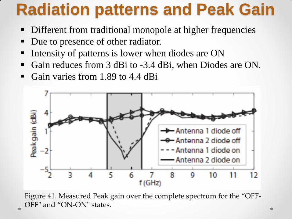
Radiation patterns and Peak Gain Different from traditional monopole at higher frequencies
Due to presence of other radiator.
Intensity of patterns is lower when diodes are ON
Gain reduces from 3 dBi to -3.4 dBi, when Diodes are ON.
Gain varies from 1.89 to 4.4 dBi
Figure 41. Measured Peak gain over the complete spectrum for the “OFF-OFF" and “ON-ON" states.

Envelope Correlation Coefficient
ECC tells how much both antennas are correlated
Less than -20 dB
Figure: Numerically calculated envelop correlation coefficient from measured S-parameters.

Proposed Design 3
Four Elements UWB-MIMOantenna with band stopdesign Dimensions are 50 x 39.8
mm2
Bandwidth from 2.7 to 12GHz, when diodes are ON,the band from 5.2 to 5.8GHz is rejected.
PIN diodes are used toconnect the band stopdesign with ground plane
Figure: Geometry of the proposed UWB-MIMO antenna (a) Top view (b) Bottom view and (c) Band-stop design. Optimised dimensions in millimetres are: w = 39.8, l = 50, w1 = 15, w2 = 5, w3 = 5, w4 = 2.26, l1 = 10, l2 = 15, l3 = 1.1, wf = 1.5, lf = 9.85, d23 = 12, d24 = 18.95, wg1 = wg2 = 13.5, wg3 = 5, lg1 = lg2 = 6.25, lg3 = 5.1, cg = 0.5, a1 = 2, a2 = 1, a3 = 5, a4 = 1, b1 = 13.7, b2 = 1.7, b3 = 5, b4 = 11.7 and b5 = 0.5.
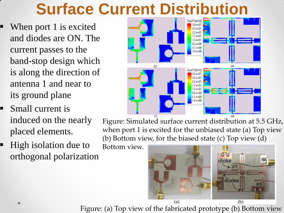
Surface Current Distribution When port 1 is excited
and diodes are ON. The
current passes to the
band-stop design which
is along the direction of
antenna 1 and near to
its ground plane
Small current is
induced on the nearly
placed elements.
High isolation due to
orthogonal polarization
Figure: Simulated surface current distribution at 5.5 GHz, when port 1 is excited for the unbiased state (a) Top view (b) Bottom view, for the biased state (c) Top view (d)Bottom view.
Figure: (a) Top view of the fabricated prototype (b) Bottom view

Simulated and Measured Results
Figure: Simulated and measured S-parameters of antenna for the PIN diodes unbiased states (a) S11 and S22 (b) Measured mutual coupling
Figure: Simulated and measured S-parameters of antenna for the PIN diodes biased states (a) S11 and S22
(b) Measured mutual coupling

Radiation pattern
Figure: Simulated and measured radiation patterns of the proposed antenna for the PIN diodes unbiased states, only port 1 was excited (a) 3 GHz, (b) 5.5 GHz, and (c) 9 GHz.
Figure : Simulated and measured radiation patterns of the proposed antenna for the PIN diodes biased states, only port 1 was excited (a) 3 GHz, (b) 5.5 GHz, and (c) 9 GHz.

Peak Gain and ECC
Figure: Simulated and measured peak gain of the proposed antenna for the PIN diodes unbiased states over complete radiating band.
Figure : Simulated and measured peak gain of the proposed antenna for the PIN diodes biased state over complete radiating band.
Figure: Numerically calculated ECC from the measured S-parameters.

Proposed Design 4
Four Elements Selflex array
A reconfigurable sensingcircuit to recover the patternon conformal surfaces
Resistors, AMP04 andflexible resistor were used todesign the sensing circuit
Input voltage was changed tochange the output and enableit to provide correct voltagefor switching frequency.
Figure: Topology of the self-adapting frequency reconfigurable conformal antenna
Figure: Schematic of the recongurable sensing circuit used to control the voltage controlled phase shifters (R 1 = 1.0 MΩ, R gain = 4.0 KΩ - connected between pins 1 and 8).
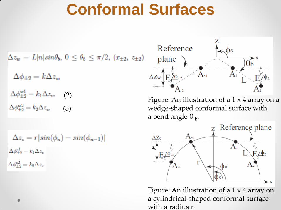
Conformal Surfaces
Figure: An illustration of a 1 x 4 array on a wedge-shaped conformal surface with a bend angle θ b.
Figure: An illustration of a 1 x 4 array on a cylindrical-shaped conformal surface with a radius r.
(2)
(3)

Simulated and Measured Results
Figure: A photograph of the prototype sensor circuit and
Figure: Normalized phase shift values measured from the Hittite phase shifters and compared to the values determined by eqns. (2) and (3) for accuracy.
Figure: (a) Drawing of the frequency reconfigurable microstrip patch element in the 1 x 4 array and (b) photograph of the prototype element (ls = 42 mm, ws = 50.5 mm, lp1 = 17.7 mm, lp2 = 4.8 mm, wp = 49 mm, lf = 17.6 mm, wf = 1.3 mm.
Figure: Measured and simulated S-parameter

Patterns on conformal surfaces
Figure: Photograph of the prototype array on the wedge-shaped conformal surface. Figure: Analytical and Measured patterns of
antenna array at 2.43 GHz (f1) in the x-z plane for the wedge-shaped conformal surface with θb = 30o.
Figure: Analytical and Measured patterns of antenna array at 3.15 GHz (f2) in the x-z plane for the wedge-shaped conformal surface with θb = 30o

Patterns and Gain
Figure: Analytical and Measured patterns of antenna array at 2.43 GHz (f 1) in the x-z plane for the cylindrical-shaped conformal surface.
Figure: Analytical and Measured patterns of antenna array at 3.15 GHz (f 2) in the x-z plane for the cylindrical-shaped conformal surface.
Figure: Measured gain of the self-adapting antenna prototypes at f 1 for θb = 30o .
Figure: Measured gain of the self-adapting antenna prototypes at f 2 for θb = 30o .

Proposed Design 5
Series Fed Array with three elements
Pin diodes are used to used to reconfigure the different CRLH-TLs for switching frequencies
The array switches from 2.37 GHz to 1.97 GHz
Broadside patterns are achieved at both switching frequencies
Figure: Layout of the reconfigurable series fed array with CRLH-TL interconnects. (a) Top view (b) Bottom view. Dimensions are: a = 43.2 mm, b = 39 mm, c = 43.7 mm, d = 39 mm, e = 44.4 mm, f = 49.5 mm, f1 = 26.5 mm, f2 = 15.3 mm, f3 = 2.7 mm, f4 = 2.5 mm, e1 = 24.7 mm, e2 = 24.5 mm, g = 1 mm, h = 2.65 mm, i = 2.7 mm, k1 = 16.9 mm, k2 = 8.2 mm, k3 = 23.8 mm, l = 12.4 mm, m = 2 mm, n1 = 3.65 mm and n2 = 4.86 mm.

Block Diagram
Metamaterials exhibit certain electromagnetic properties which
are not found in nature.
Left handed materials having properties of negative permeability
and permittivity
Veselago in 1967 was the first physicist who realized the
concepts of left handed materials (LHM).
Figure: (a) Circuit representation of a 3-element series-fed array with conventional microstrip interconnects and (b) circuit representation of a 3-element series-fed array with CRLH-TL interconnections showing the switching mechanism.
Figure: (a) Layout of CRLH-TL unit cell 1. (b) Layout of CRLH-TL unit cell 2. (c) Circuit representation of CRLH-TL Unit Cells. Dimensions are: k = 11.9 mm, k1 = 16.9 mm, k2 = 8.2 mm, k3 = 23.8 mm, S = 1.3 mm, t = 7.26 mm.

Zero Phase Diagram
Figure: Simulated S12 phase for the conventional transmission line with a total length of k1+k+k2, higher band (unit cell 1) and lower band (unit cell 2).

Surface Current
Figure: Picture of the manufactured prototype.
Figure: Surface current distribution for (a) 1.97GHz and (b) 2.37GHz.

Simulated and Measured Results
Figure: Simulated and measured S 11 for the lower band with S1 activated.
Figure: Simulated and measured S 11 for the lower band with S2 activated.
Figure: Simulated and measured radiation pattern in the y-z plane for (a) 1.97GHz and (b) 2.37GHz.

Conclusions
Five different reconfigurable antennas are designed.
Frequency reconfigurable antenna
Two elements UWB-MIMO antenna with WLAN rejection
Four elements UWB-MIMO antenna with WLAN rejection
Frequency reconfigurable self adapting antenna array
Three elements series fed array with CRLH-TLs
PIN diodes are used to reconfigure these antennas.

Challenges and Future Directions
Challenges
Losses due to active elements
Power consumption due to active elements
Mismatch between simulated and measured results
Future Directions
MEMS switches with fast switching and low input voltage
Magnetic switches
New applications (dual polarized omni-directional MIMOantennas)

Acknowledgement
Cariparo Foundation
Prof. Antonio Capobianco
Prof. Benjamin Braaten

Bibliography[1] G.A. Deschamps, “Microstrip Microwave Antennas,” 3rd USAF Symposium on Antennas, 1953.[2] David M. Pozar and Daniel H. Schaubert, “Microstrip Antennas: The analysis and Design of Microstrip Antennas and Arrays,” IEEE Press, Piscataway, NJ, 1995.
[3] Warren L. Stutzman and Gary A. Thiele, “Antenna Theory and Design,” 2nd ed., John Wiley and Sons, Inc., New York, 1998.
[4] D. Schaubert, B, “Frequency-agile polarization diversity microstrip antennas and frequency scanned arrays,” U.S. Patent 4 367 474, Jan. 1983.
[5] J. K. Smith, “Reconfigurable aperture antenna (RECAP),” DARPA, 1999. [Online Available]: www.darpa.mil[6] J. Costantine, “Design, optimization and analysis of reconfigurable antennas,” Ph.D. dissertation, Electr. Comput. Eng. Dept., Univ. New Mexico (UNM), Albuquerque, NM, Dec. 2009.
[7] C. W. Jung, et. all, “Reconfigurable scan-beam single-arm spiral antenna integrated with RF-MEMS switches,” IEEE Trans. Antennas Propag., vol. 54, no. 2, pp. 455-463, Feb. 2006.[8] S. Shelley, J. Costantine, C. G. Christodoulou, D. E. Anagnostou, and J. C. Lyke, “FPGA-controlled switch-reconfigured antenna,” IEEE Antennas Wireless Propag. Lett., vol. 9, pp. 355-358, 2010.
[9] C. R. White and G. M. Rebeiz, “Single and dual-polarized tunable slot-ring antennas,” IEEE Trans. Antennas Propag., vol. 57, no. 1, pp. 19-26, Jan. 2009.
[10] C. J. Panagamuwa, A. Chauraya, and J. C. Vardaxoglou, “Frequency and beam reconfigurable antenna using photoconductive switches,” IEEE Trans. Antennas Propag., vol. 54, no. 2, pp. 449-454, Feb. 2006.
[11] Y. Tawk, A. R. Albrecht, S. Hemmady, G. Balakrishnan, and C. G. Christodoulou, “Optically pumped frequency reconfigurable antenna design,” IEEE Antennas Wireless Propag. Lett., vol. 9, pp. 280-283, 2010.
[12] Y. Tawk, J. Costantine, S. E. Barbin, and C. G. Christodoulou, “Integrating laser diodes in a reconfigurable antenna system,” in Proc. SBMO/IEEE MTT-S Int. Microw. Optoelectron. Conf., Oct. 2011.
[13] S. Jalali Mazlouman, M. Soleimani, A. Mahanfar, C. Menon, and R. G. Vaughan, “Pattern reconfigurable square ring patch antenna actuated by hemispherical dielectric elastomer,” Electron. Lett., vol. 47, no. 3, pp. 164-165, Feb. 2011.

Any Question?