Recent progress on SuNAM’s coated conductor development ...
39
Recent progress on SuNAM’s coated conductor development; performance, price & utilizing ways Superconductor, Nano & Advanced Materials Seung Hyun Moon, Jae-Hoon Lee & Hunju Lee SuNAM Co., Ltd. 2016. 09. 13. CCA 2016, Aspen, Colorado, US. IEEE/CSC & ESAS EUROPEAN SUPERCONDUCTIVITY NEWS FORUM (global edition), October 2016. Presentation IO-16 given at CCA 2016; Aspen, Colorado,USA, September 11 – 14, 2016. 1
Transcript of Recent progress on SuNAM’s coated conductor development ...

Recent progress on SuNAM’s coated conductor
development; performance, price & utilizing ways
Superconductor, Nano & Advanced Materials
Seung Hyun Moon, Jae-Hoon Lee & Hunju Lee
SuNAM Co., Ltd.
2016. 09. 13.
CCA 2016, Aspen, Colorado, US.
IEEE/CSC & ESAS EUROPEAN SUPERCONDUCTIVITY NEWS FORUM (global edition), October 2016. Presentation IO-16 given at CCA 2016; Aspen, Colorado,USA, September 11 – 14, 2016. 1

SuNAM’s coated conductor; architecture, characteristic. Quality control tools for uniformity and yield
Higher Je : Thicker S.C. layer 1.6 m, >1,000 A/12 mm.
MCI(Metal Clad Insulation) 2G wire for high field magnet.
Solution for charging time delay problem in NI(No-Insulation) coil.
Higher Je : metal substrate removal process.
Summary
Contents
IEEE/CSC & ESAS EUROPEAN SUPERCONDUCTIVITY NEWS FORUM (global edition), October 2016. Presentation IO-16 given at CCA 2016; Aspen, Colorado,USA, September 11 – 14, 2016. 2

SuNAM’s Coated Conductor
IEEE/CSC & ESAS EUROPEAN SUPERCONDUCTIVITY NEWS FORUM (global edition), October 2016. Presentation IO-16 given at CCA 2016; Aspen, Colorado,USA, September 11 – 14, 2016. 3

IEEE/CSC & ESAS EUROPEAN SUPERCONDUCTIVITY NEWS FORUM (global edition), October 2016. Presentation IO-16 given at CCA 2016; Aspen, Colorado,USA, September 11 – 14, 2016. 4
스티커 노트
HTS wire requirements in performance and price for various application devices were being studied at least for 10 years.
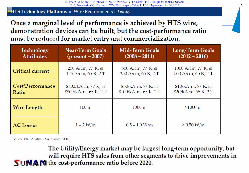
IEEE/CSC & ESAS EUROPEAN SUPERCONDUCTIVITY NEWS FORUM (global edition), October 2016. Presentation IO-16 given at CCA 2016; Aspen, Colorado,USA, September 11 – 14, 2016. 5
스티커 노트
Unfortunately, performance and price goals have not been met until recently.

Applications of Superconductivity
Can carry extremely large current without loss. Can generated extremely large magnetic field. High energy efficiency with compact volume & mass.
Current carry
HTS 2G Wire
NMR
MRI Crystal growth
Magnetic seperator
Motor
MagLev
FCL Motor & Generator Transformer
Cable
Fusion
Switcing
Wind
Generator
Biz Chance
in near(?) future
IEEE/CSC & ESAS EUROPEAN SUPERCONDUCTIVITY NEWS FORUM (global edition), October 2016. Presentation IO-16 given at CCA 2016; Aspen, Colorado,USA, September 11 – 14, 2016. 6
스티커 노트
Electric power devices such as superconducting cables and fault current limiters are beginning to be deployed on commercial basis, and coil-based applications such as rotating machines and MRI/NMR are thought to be the next candidate.

Throughput : growth rate & large deposition area
Yield : process margin & (in-line) Quality Control
Robustness : shelf life, stability (mechanical,
thermal cycling, thermal expansion…)
Customer friendly : joints, easy to use…
In-line production, automation…
For reasonable size market creation,
Target price ($/kA-m) : 50, 25, or less?
Availability : ~ 1,000 km/yr or /month or ??
RCE DR : ~ 100 nm/sec or faster (SuNAM) The highest throughput process
RCE-DR process : easy to scale-up to wide strip.
How can we realize practical HTS 2G wire?
IEEE/CSC & ESAS EUROPEAN SUPERCONDUCTIVITY NEWS FORUM (global edition), October 2016. Presentation IO-16 given at CCA 2016; Aspen, Colorado,USA, September 11 – 14, 2016. 7
스티커 노트
Manufacturing cost of 2G wire surely depends on production/sales volume, but ultimately, among the variety of manufacturing processes currently employed, high throughput process should dominate. Reactive Co-evaporation enables high throughput production due to high deposition rate and scalability to wider tapes.

Structure
- Typical Ic ~ > 700A/12mmW at 77K Self-field (Jc ~ >5 MA/cm2)
IEEE/CSC & ESAS EUROPEAN SUPERCONDUCTIVITY NEWS FORUM (global edition), October 2016. Presentation IO-16 given at CCA 2016; Aspen, Colorado,USA, September 11 – 14, 2016. 8
스티커 노트
Materials, deposition methods, thicknesses, and functions of each layer constituting 2G wire.

Scale up Issues: IBAD & in-Situ High Rate E-Beam
Robert H. Hammond (Stanford Univ.)
New Ideas, Directions?
High rate, large area, high IC and low cost of
materials processes will eventually be required –
not immediately but in 10 years.
High rate may require growth in liquid flux.
Cost Example
IEEE/CSC & ESAS EUROPEAN SUPERCONDUCTIVITY NEWS FORUM (global edition), October 2016. Presentation IO-16 given at CCA 2016; Aspen, Colorado,USA, September 11 – 14, 2016. 9
스티커 노트
Among the many factors influencing price performance ratio($/kAm), high deposition rate can be achieved with the help of liquid flux which exists at a certain area in the phase diagram.
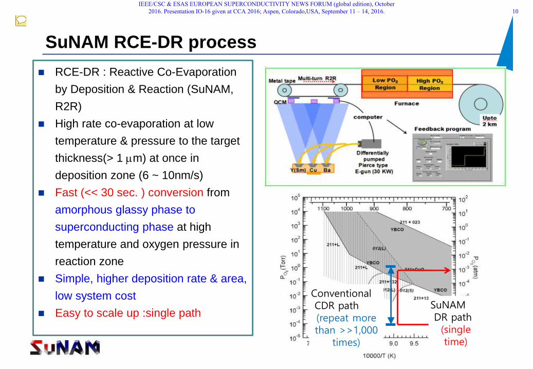
SuNAM RCE-DR process
RCE-DR : Reactive Co-Evaporation
by Deposition & Reaction (SuNAM,
R2R)
High rate co-evaporation at low
temperature & pressure to the target
thickness(> 1 m) at once in
deposition zone (6 ~ 10nm/s)
Fast (<< 30 sec. ) conversion from
amorphous glassy phase to
superconducting phase at high
temperature and oxygen pressure in
reaction zone
Simple, higher deposition rate & area,
low system cost
Easy to scale up :single path SuNAM DR path
(single time)
Conventional CDR path (repeat more than >>1,000
times)
IEEE/CSC & ESAS EUROPEAN SUPERCONDUCTIVITY NEWS FORUM (global edition), October 2016. Presentation IO-16 given at CCA 2016; Aspen, Colorado,USA, September 11 – 14, 2016. 10
스티커 노트
Lower right graph depicts the path taken by amorphous precursor of Gd2O3, BaO, CuOx mixture in the T-PO2 phase diagram, and upper right schematic shows how we realize the path.

Superconductor, Nano & Advanced Materials
500 nm
Gd
Ba
Cu
O
Cu
Cu
Cu
Cu Gd
Ba
Cu
O
O
Cu Cu
Gd
Ba O
O
L
Gd2O3
GdBCO
Gd2O3
Cu-O
• Very low PO2 zone (~ 10-5 Torr): Amorphous Film
• Lower PO2 zone (~30 mTorr): Gd2O3 + Liquid (< 5 sec)
• Higher PO2 zone (~100 mTorr): GdBCO Film (< 20 sec)
GdBCO growth mechanism: a seeded melt-textured growth!!!
Growth mechanism of the GdBCO film by RCE-DR
IEEE/CSC & ESAS EUROPEAN SUPERCONDUCTIVITY NEWS FORUM (global edition), October 2016. Presentation IO-16 given at CCA 2016; Aspen, Colorado,USA, September 11 – 14, 2016. 11
스티커 노트
You can see how the Gd2O3 seed in the BaCuO liquid nucleates GdBaCuO (right) as the precursor sweeps the path in the phase diagram (left) (I’m sorry that PPT animation cannot be seen in PDF format.)

Daily Production 2G wire performances
0 100 200 300 400 500 600 7000
100
200
300
400
500
600
700
800
900
1000
Ic (
A / 1
2 m
m )
Length ( m )
0 100 200 300 400 500 600 7000
100
200
300
400
500
600
700
800
900
1000
Ic (
A / 1
2 m
m )
Length ( m )
0 100 200 300 400 500 600 7000
100
200
300
400
500
600
700
800
900
1000
Ic (
A / 1
2 m
m )
Length ( m )
0 100 200 300 400 500 6000
100
200
300
400
500
600
700
800
900
1000
Ic (
A / 1
2 m
m )
Length ( m )
0 100 200 300 400 500 600 7000
100
200
300
400
500
600
700
800
900
1000
Ic (
A / 1
2 m
m )
Length ( m )
0 100 200 300 400 500 600 7000
100
200
300
400
500
600
700
800
900
1000
Ic (
A / 1
2 m
m )
Length ( m )0 100 200 300 400 500 600 700
0
100
200
300
400
500
600
700
800
900
1000
Ic (
A / 1
2 m
m )
Length ( m )
0 100 200 300 400 500 600 7000
100
200
300
400
500
600
700
800
900
1000
Ic (
A / 1
2 m
m )
Length ( m )
0 100 200 300 400 500 600 7000
100
200
300
400
500
600
700
800
900
1000
Ic (
A / 1
2 m
m )
Length ( m )
Length
(m) IC IC,max IC,min 1 sigma
739 820 857 761 1.7
Length
(m) IC IC,max IC,min 1 sigma
700 800 865 615 3.4
Length
(m) IC IC,max IC,min 1 sigma
682 801 860 654 3.2
Length
(m) IC IC,max IC,min 1 sigma
734 810 856 713 2.2
Length
(m) IC IC,max IC,min 1 sigma
728 820 866 729 2.4
Length
(m) IC IC,max IC,min 1 sigma
710 804 859 716 2.5
Length
(m) IC IC,max IC,min 1 sigma
718 800 869 707 3.6
Length
(m) IC IC,max IC,min 1 sigma
743 803 840 651 1.8
Length
(m) IC IC,max IC,min 1 sigma
743 813 847 768 1.6
( ~ 6 hrs deposition time (120 m/hr))
IEEE/CSC & ESAS EUROPEAN SUPERCONDUCTIVITY NEWS FORUM (global edition), October 2016. Presentation IO-16 given at CCA 2016; Aspen,,Colorado,USA, September 11 – 14, 2016. 12
스티커 노트
We typically produce ~700 meters of wire in a single run with the speed of ~ 120 m/hr (12 mm wide tape). Ic variations along the lengths are shown for 9 runs.
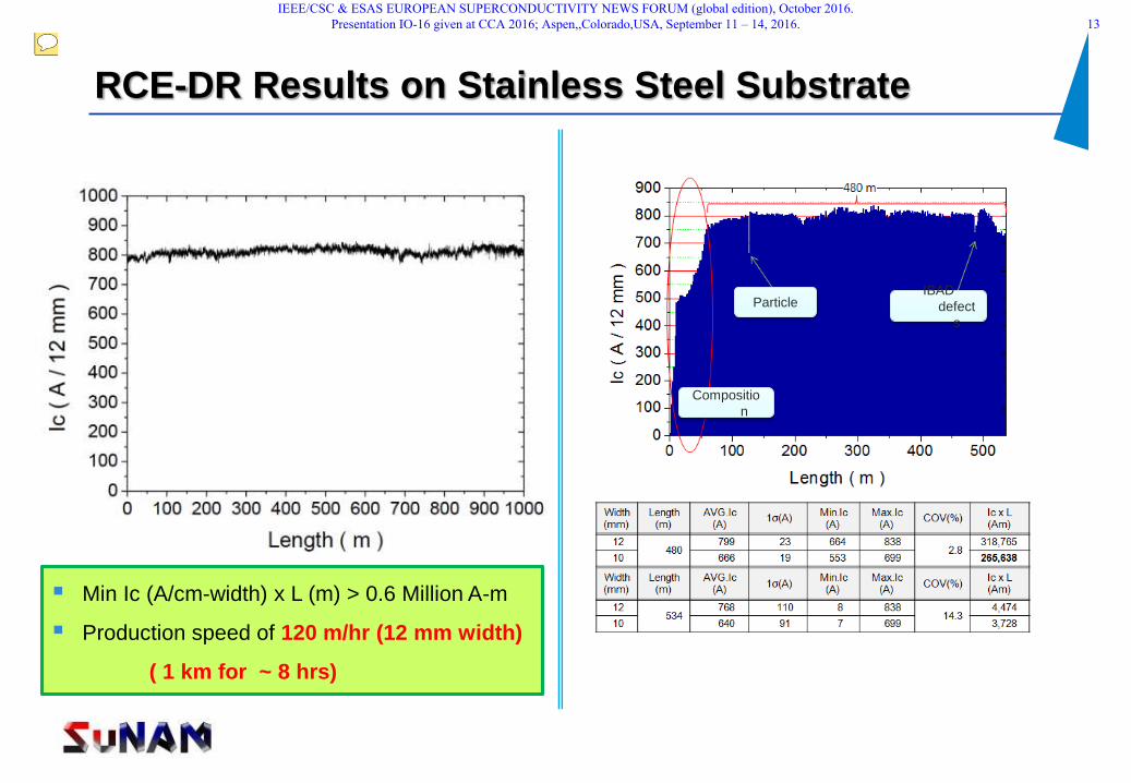
RCE-DR Results on Stainless Steel Substrate
Min Ic (A/cm-width) x L (m) > 0.6 Million A-m
Production speed of 120 m/hr (12 mm width)
( 1 km for ~ 8 hrs)
Particle IBAD
defect
s
Compositio
n
IEEE/CSC & ESAS EUROPEAN SUPERCONDUCTIVITY NEWS FORUM (global edition), October 2016. Presentation IO-16 given at CCA 2016; Aspen,,Colorado,USA, September 11 – 14, 2016. 13
스티커 노트
Some point defects, the origin of which we can trace, and rather slow composition variations are not totally under control upto now.

<QCM Feedback program>
<RHEED spot Feedback program>
Control computer
An appropriate feedback algorithm can keep the shape of the RHEED spot in the
specific range, while QCM monitoring to adjust the e-gun power.
Before optimization After optimization
Quality Control : RHEED Vision System
IEEE/CSC & ESAS EUROPEAN SUPERCONDUCTIVITY NEWS FORUM (global edition), October 2016. Presentation IO-16 given at CCA 2016; Aspen,,Colorado,USA, September 11 – 14, 2016. 14
스티커 노트
In-line quality control is very important for producing high quality wire with minimal number of defects and/or non-uniformity. This page describes how we maintain the crystallinity of IBAD-MgO with RHEED pattern as a feedback input.

14
67 68 69 70 71 72 73 74 75 76 77
2.8
3.0
3.2
3.4
3.6
3.8
4.0
(
deg
ree)
Rheed Spot Angle (degree)
6.0
6.2
6.4
6.6
6.8
7.0
(d
eg
ree)
Feedback route based on RHEED spot analysis
(110) spot
Because of different evolution of & R,
optimization is very important for high quality 2G
wire.
Intensity & tilt angle of MgO (110) spot is one of the
most important parameter.
IEEE/CSC & ESAS EUROPEAN SUPERCONDUCTIVITY NEWS FORUM (global edition), October 2016. Presentation IO-16 given at CCA 2016; Aspen,,Colorado,USA, September 11 – 14, 2016. 15
스티커 노트
In-plane and out-of-plane crystallinity (Δϕ and Δω) behave differently with respect to RHEED spot angle, forcing us to compromise.

Quality Control : RCE Vision Inspection System
Based on color dependence of composition DB, optimum composition level is automatically controlled by PC. (Slow feedback)
IEEE/CSC & ESAS EUROPEAN SUPERCONDUCTIVITY NEWS FORUM (global edition), October 2016. Presentation IO-16 given at CCA 2016; Aspen,,Colorado,USA, September 11 – 14, 2016. 16
스티커 노트
With the knowledge that the surface color (RGB) of the SC layer has a strong correlation with composition (RE:Ba:Cu), we set up another feedback system for the SC layer.

[Start] [End]
Start color
End color
RCE Vision System will be introduced for increasing the uniformity of composition in
RCE-DR process. The control computer takes (RGB) values in three-dimensional
vector space which is transformed from the color of the tape surface.
Control
the power
Color detection
Is the (RGB) vector
in the range?
Yes
No
Quality Control : RCE Vision Inspection System
(Composition DB)
IEEE/CSC & ESAS EUROPEAN SUPERCONDUCTIVITY NEWS FORUM (global edition), October 2016. Presentation IO-16 given at CCA 2016; Aspen,,Colorado,USA, September 11 – 14, 2016. 17
스티커 노트
The feedback system reads RGB of surface, looks up DB to figure out the composition, and then adjust the deposition rate of each metal accordingly, until the desired composition/color is restored.

Higher Je : Thicker S.C. layer
IEEE/CSC & ESAS EUROPEAN SUPERCONDUCTIVITY NEWS FORUM (global edition), October 2016. Presentation IO-16 given at CCA 2016; Aspen,,Colorado,USA, September 11 – 14, 2016. 18

18 Normal RCE-DR process : before optimization
1.2 1.4 1.6 1.8 2.0 2.20
100
200
300
400
500
600
700
800
I C (
A/1
2 m
m)
Thickness (m)
IC
0
1
2
3
4
5
6
JC
JC (M
A/c
m2)
Thickness dependence of Ic and surface color for GdBCO
1 2 3 4 5
Thickness 1.3㎛ 1.6㎛ 1.8㎛ 2.0㎛ 2.2㎛
Surface color for GdBCO
Ic 750A/12mm 600A/12mm 300A/12mm 100A/12mm 0A/12mm
TEM analysis
→ 1.3 ㎛-thickness:
Gd2O3 are randomly distributed
→ 1.9 ㎛-thickness:
Gd2O3 are distributed the boundary of the layers
1
2 3
As increasing the thickness, Jc and Ic are decreased. All the samples were prepared by same process speed.
IEEE/CSC & ESAS EUROPEAN SUPERCONDUCTIVITY NEWS FORUM (global edition), October 2016. Presentation IO-16 given at CCA 2016; Aspen,,Colorado,USA, September 11 – 14, 2016. 19
스티커 노트
When the deposition rate(=thickness of superconducting layer) is increased, both Ic and Jc are sharply reduced

Optimization of deposition region for making thick GdBCO films
For uniformity, 1. Decrease deposition region from 55 cm to
45 cm. 2. Increase distance between source and
substrate. 3. Increasing turns of deposition region (14
turns 19 turns)
14 19
As increasing the thickness, Jc is decreased
As increasing the thickness, Jc is not decreased
1.6 m-thick
All the samples were prepared by same process speed.
IEEE/CSC & ESAS EUROPEAN SUPERCONDUCTIVITY NEWS FORUM (global edition), October 2016. Presentation IO-16 given at CCA 2016; Aspen,,Colorado,USA, September 11 – 14, 2016. 20
스티커 노트
We found the deposition region in which all the compositions (RE, Ba, Cu) can be uniformly deposited and increased the number of turns in order to increase the thickness of the superconducting layer.
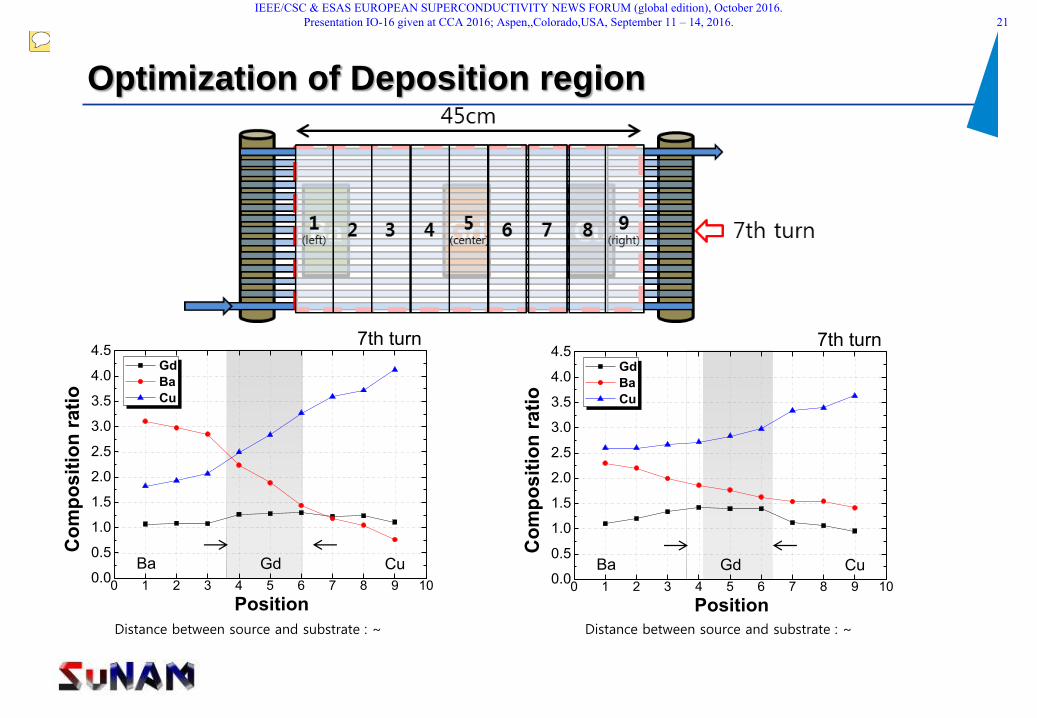
0 1 2 3 4 5 6 7 8 9 100.0
0.5
1.0
1.5
2.0
2.5
3.0
3.5
4.0
4.5
Gd Cu
Co
mp
os
itio
n r
ati
o
Gd
Ba
Cu
Position
Ba
7th turn
0 1 2 3 4 5 6 7 8 9 100.0
0.5
1.0
1.5
2.0
2.5
3.0
3.5
4.0
4.5
Gd Cu
Co
mp
os
itio
n r
ati
o
Gd
Ba
Cu
Position
Ba
7th turn
Optimization of Deposition region
Distance between source and substrate : ~ Distance between source and substrate : ~
IEEE/CSC & ESAS EUROPEAN SUPERCONDUCTIVITY NEWS FORUM (global edition), October 2016. Presentation IO-16 given at CCA 2016; Aspen,,Colorado,USA, September 11 – 14, 2016. 21
스티커 노트
In addition, the metal sources (RE, Ba, Cu) are put further away from the substrate to increase the deposition uniformity.

0 100 200 300 400 500 600 700 800 900 1000
0.0
2.0x10⁻⁵
4.0x10⁻⁵
6.0x10⁻⁵
8.0x10⁻⁵
1.0x10⁻⁴
Criteria = V/cm
IC = 905 A / 12 mm
N-value = 44.2
V (
Volt
age
)
I ( A / 12 mm )
(77 K, s.f.)
0 20 40 60 80 1000
200
400
600
800
1000
1200
I C (
A )
Position(m)
Optimization of RCE-DR process for thick superconducting layer
IEEE/CSC & ESAS EUROPEAN SUPERCONDUCTIVITY NEWS FORUM (global edition), October 2016. Presentation IO-16 given at CCA 2016; Aspen,,Colorado,USA, September 11 – 14, 2016. 22

RCE-DR results (with optimization deposition region)
1,050A/12mm-w
(→ 875A/cm-w)
>800A/cm
0 200 400 600 800 1000 1200
0.0
1.0x10⁻⁵
2.0x10⁻⁵
3.0x10⁻⁵
4.0x10⁻⁵
5.0x10⁻⁵
6.0x10⁻⁵
Vo
ltag
e (
V)
Current (A)
@ 77 K, self-field
Speed
(m/min) Turns
Thickness
(㎛)
IC
(A/cm)
JC
(MA/cm2)
2 14 1 500 5
2 14 1.3 600 4.6
2 14 1.9 400 2.1
2 16 1.6 800 5
2 > 20 2 ~ 2.5 > 1,000 > 5
2016 Plan for making 400 A / 4 mm CC
0.8 1.0 1.2 1.4 1.6 1.8 2.0 2.20
200
400
600
800
1000
1200
1400
IC
I C (
A/1
2 m
m)
Thickness (m)
0
1
2
3
4
5
6
7
JC
JC (M
A/c
m2)
plan
plan
results
1.6 m-thick 5.5 MA/cm2
0 100 200 300 400 500 600 700 800 900 10000
200
400
600
800
1000
I C (
A/c
m)
Length (m)
1,000 A/12 mm
The same process speed(120 m/hr ).
IEEE/CSC & ESAS EUROPEAN SUPERCONDUCTIVITY NEWS FORUM (global edition), October 2016. Presentation IO-16 given at CCA 2016; Aspen,,Colorado,USA, September 11 – 14, 2016. 23
스티커 노트
We have achieved Ic = 1,050 A/12mm-width by applying the optimal deposition region. We are now working to attain Ic = 1,200 A/12mm-width in the second half of 2016.
MCI(Metal Clad Insulation) 2G wire
for high field magnet
IEEE/CSC & ESAS EUROPEAN SUPERCONDUCTIVITY NEWS FORUM (global edition), October 2016. Presentation IO-16 given at CCA 2016; Aspen,,Colorado,USA, September 11 – 14, 2016. 24

Multi-width Double Pancake Coils
Stacked Double
Pancake Coils Fully assembled
No-insulation, multi-width, and compact !
4.1mmW 5.1mmW 6.1mmW 7.1mmW 8.1mmW
327 m
m
O.D. 172mm
I.D. 35mm Immersed in liquid Helium
26.4 T all 2G wire one-body(non-nested) magnet
(Designed by S. Hahn (MIT NHMFL/FSU)
IEEE/CSC & ESAS EUROPEAN SUPERCONDUCTIVITY NEWS FORUM (global edition), October 2016. Presentation IO-16 given at CCA 2016; Aspen,,Colorado,USA, September 11 – 14, 2016. 25
스티커 노트
Through a collaboration with Prof. S. Hahn, we succeeded in manufacturing HTS magnet, generating 26.4 T of center field at liquid Helium temp. This magnet is the first one wound only with 2G HTS wire in non-nested fashion, that generated such a high field.

NI-MW winding technic – No insulation
No-insulation winding technic :
Pros :
Compactness : without thick stabilizer
Strong mechanical strength : without soft insulation material
Self protection : automatic bypass
Rapid quench propagation
“Automatic bypass”
of the exceeding
current and better
protection to quench Without insulation
Quench
bypass current
(by S. Y. Hahn)
𝑄𝑅𝐶 W = 𝐼𝑅
2 ∙ 𝑅𝐶
where, 𝐼𝑅 = 𝐼𝑃𝑆 − 𝐼𝜃 = 𝐼𝑃𝑆 −𝐵0
𝑘0
Cons :
Charging time delay.
(excess heat generation/
Impractically slow for
charging)
(by S. Hahn)
IEEE/CSC & ESAS EUROPEAN SUPERCONDUCTIVITY NEWS FORUM (global edition), October 2016. Presentation IO-16 given at CCA 2016; Aspen,,Colorado,USA, September 11 – 14, 2016. 26
스티커 노트
Pros and cons of no-insulation winding, and an equivalent circuit which is very useful in describing the behavior.
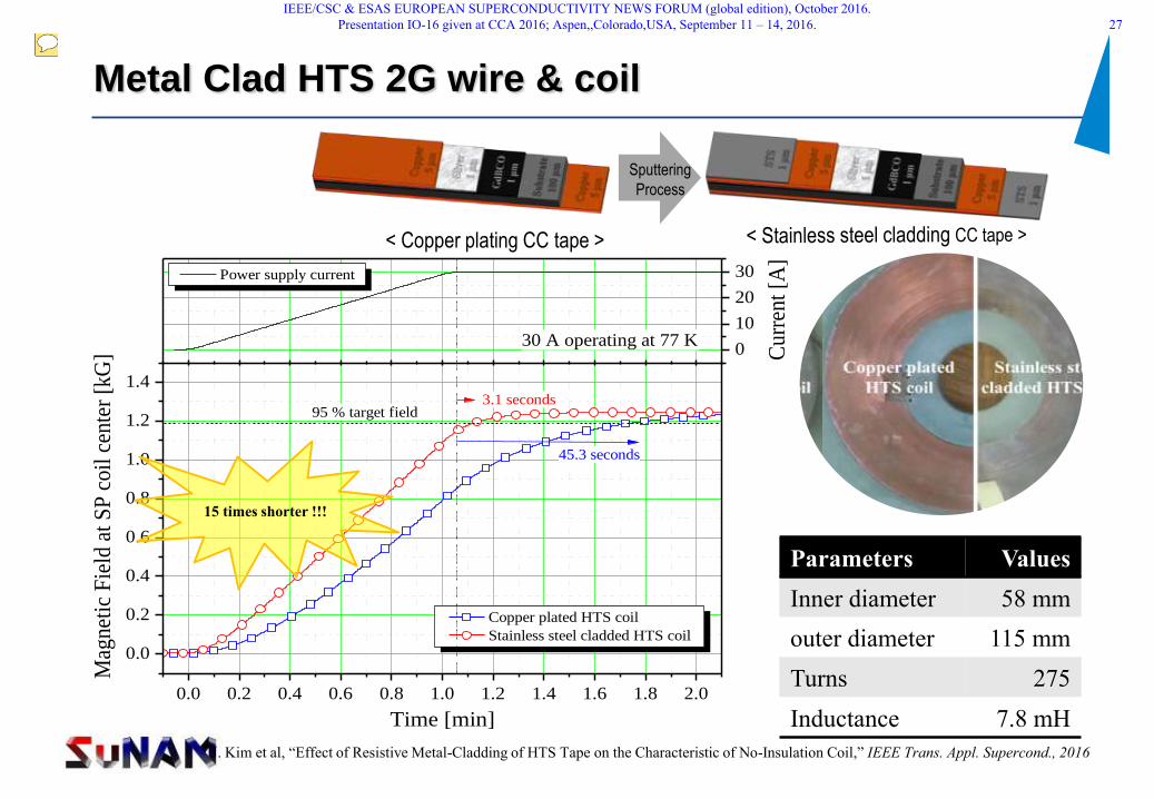
Metal Clad HTS 2G wire & coil
0
10
20
30 Power supply current
Cu
rren
t [A
]
30 A operating at 77 K
0.0 0.2 0.4 0.6 0.8 1.0 1.2 1.4 1.6 1.8 2.0
0.0
0.2
0.4
0.6
0.8
1.0
1.2
1.4
45.3 seconds
3.1 seconds
Copper plated HTS coil
Stainless steel cladded HTS coil
Mag
net
ic F
ield
at
SP
co
il c
ente
r [k
G]
Time [min]
95 % target field
15 times shorter !!!
J. Kim et al, “Effect of Resistive Metal-Cladding of HTS Tape on the Characteristic of No-Insulation Coil,” IEEE Trans. Appl. Supercond., 2016
Parameters Values
Inner diameter 58 mm
outer diameter 115 mm
Turns 275
Inductance 7.8 mH
< Copper plating CC tape >
Sputtering
Process
IEEE/CSC & ESAS EUROPEAN SUPERCONDUCTIVITY NEWS FORUM (global edition), October 2016. Presentation IO-16 given at CCA 2016; Aspen,,Colorado,USA, September 11 – 14, 2016. 27
스티커 노트
Charging delay, one drawback of the no-insulation coil, can be reduced by metal-cladding to the tapes, adding extra resistance between turns.

Burn out test @ 77 K ( SPC with Copper stabilizer vs. MCI )
0 2 4 6 8 10 12 14 16 18 20 22 24 26 28 30
0
50
100
150
200
250
300
350
400
450
5007.3 I
c Current
Voltage
Field
Time [min]
Cu
rren
t [A
]
EPL DPC Quench @ 473 [A]
Ic = 65 A
-0.25
-0.20
-0.15
-0.10
-0.05
0.00
0.05
0.10
0.15
0.20
0.25
Voltage
[V]
0.0
0.5
1.0
1.5
2.0
2.5
3.0
3.5
4.0
4.5
5.0
Field
[kG]
0 2 4 6 8 10 12 14 16 18 20 22 24 26 28 30
0
50
100
150
200
250
300
350
400
450
500
SUS DPC Quench @ 420 [A]
Current
Voltage
Field
Time [min]
Curr
ent
[A]
0
1
2
3
4
5
6
7
8
9
10
Voltage
[V]
0.0
0.5
1.0
1.5
2.0
2.5
3.0
3.5
4.0
4.5
5.0
Field
[kG]
Ic = 65 A
6.5 Ic
IEEE/CSC & ESAS EUROPEAN SUPERCONDUCTIVITY NEWS FORUM (global edition), October 2016. Presentation IO-16 given at CCA 2016; Aspen,,Colorado,USA, September 11 – 14, 2016. 28
스티커 노트
Added resistance reduced charging delay, but did not compromise quench stability.

Magnet Operation Results
Time constant, t, is calculated to 11 seconds.
Contact resistance between turns, RS,STS = 165 [W·cm2]
(By J. Kim et. al., CP-14, yesterday)
IEEE/CSC & ESAS EUROPEAN SUPERCONDUCTIVITY NEWS FORUM (global edition), October 2016. Presentation IO-16 given at CCA 2016; Aspen,,Colorado,USA, September 11 – 14, 2016. 29
스티커 노트
We adopted metal-cladded tapes to 3 T demo magnet which is a scale-down version of 9.4 T/400 MHz NMR magnet.

STS cladded tape Charging time is 41 times shorter
Reduction of Charging Delay
If magnet was wound with copper plated tape,
(By J. Kim et. al., CP-14, yesterday)
IEEE/CSC & ESAS EUROPEAN SUPERCONDUCTIVITY NEWS FORUM (global edition), October 2016. Presentation IO-16 given at CCA 2016; Aspen,,Colorado,USA, September 11 – 14, 2016. 30
스티커 노트
Reduction of charging delay is impressive.

Higher Je : metal substrate removal
process
IEEE/CSC & ESAS EUROPEAN SUPERCONDUCTIVITY NEWS FORUM (global edition), October 2016. Presentation IO-16 given at CCA 2016; Aspen,,Colorado,USA, September 11 – 14, 2016. 31
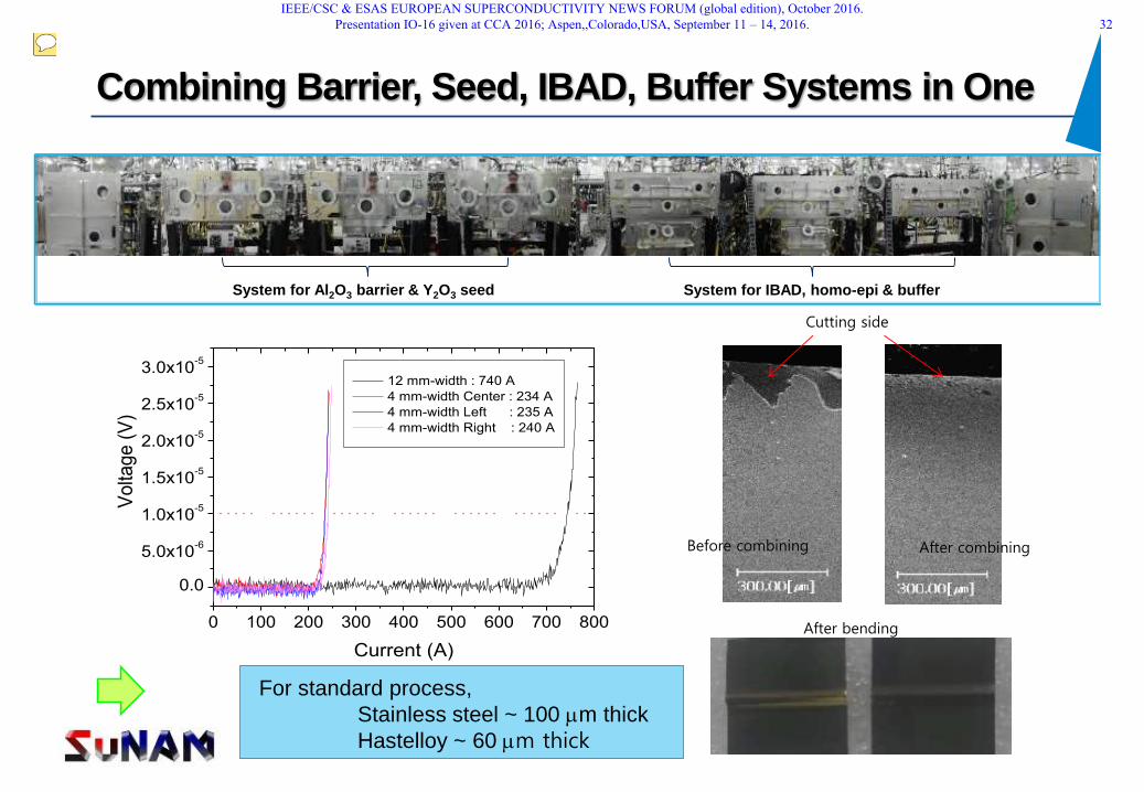
Before combining After combining
0 100 200 300 400 500 600 700 800
0.0
5.0x10⁻⁶
1.0x10⁻⁵
1.5x10⁻⁵
2.0x10⁻⁵
2.5x10⁻⁵
3.0x10⁻⁵
12 mm-width : 740 A
4 mm-width Center : 234 A
4 mm-width Left : 235 A
4 mm-width Right : 240 A
Volta
ge (
V)
Current (A)
Cutting side
After bending
System for Al2O3 barrier & Y2O3 seed System for IBAD, homo-epi & buffer
Combining Barrier, Seed, IBAD, Buffer Systems in One
For standard process,
Stainless steel ~ 100 m thick
Hastelloy ~ 60 m thick
IEEE/CSC & ESAS EUROPEAN SUPERCONDUCTIVITY NEWS FORUM (global edition), October 2016. Presentation IO-16 given at CCA 2016; Aspen,,Colorado,USA, September 11 – 14, 2016. 32
스티커 노트
We connected IBAD and sputtering (deposition process of Al2O3, Y2O3) to build an in-line system for prevention of contamination by external exposure. -> Improvement of adhesive property of coated conductor

Utilize this properties !!
IEEE/CSC & ESAS EUROPEAN SUPERCONDUCTIVITY NEWS FORUM (global edition), October 2016. Presentation IO-16 given at CCA 2016; Aspen,,Colorado,USA, September 11 – 14, 2016. 33
스티커 노트
We utilize small the value of the peel/cleavage stress, which sometimes degrade the performance of impregnated coils, to our advantage. We cleave the 2G tape such that the SC layer sticks to the thin protecting layer rather than to the thick substrate.

High Je wire by removal of thick metal substrate
For Je, substrate thickness must be thin
Superconductor layer
Substrate
Stabilizer
For thin substrate, easy to damage during the reel
to reel process
Superconductor layer
Substrate
Stabilizer
Soldering thin substrate
on top of CC
Remove bottom substrate
Improvement of Je
4 roll 도면 or 사진
Intentionally making a weak interface
by some treatment
IEEE/CSC & ESAS EUROPEAN SUPERCONDUCTIVITY NEWS FORUM (global edition), October 2016. Presentation IO-16 given at CCA 2016; Aspen,,Colorado,USA, September 11 – 14, 2016. 34
스티커 노트
Schematic of peel/cleavage process and how and where we invoke cleavage.

Demonstration of High Je wire by removal of thick metal substrate
0 2 4 6 8 10 120
50
100
150
200
250
300
I C (
A/4
mm
)
Position (m)
0 2 4 6 8 10 120
50
100
150
200
250
300
I C (
A/4
mm
)
Position (m)
45 m-thick (brass)
100 m-thick
Removing
Bottom
Substrate
Laminated
CC
Substrate
Removed
CC
Bottom
Substrate
Laminated
CC
Substrate
Removed
CC
Substrate remove machine
- Easily reduce the thickness ~ < 20 m
- Choice of any materials(SUS, Copper…)
May possible…
2 m
5 m
20 m
Superconductor
layer
Stabilizer
Superconductor
layer
Stabilizer
Laminated
Substrate
Laminated
Substrate
IEEE/CSC & ESAS EUROPEAN SUPERCONDUCTIVITY NEWS FORUM (global edition), October 2016. Presentation IO-16 given at CCA 2016; Aspen,,Colorado,USA, September 11 – 14, 2016. 35
스티커 노트
Resulting tapes, tape performances, and apparatus for the processing.

SuNAM has been producing high IC coated conductors consistently.
Introduction of in-line Q.C. measures enhanced wire uniformity &
production yield.
With thicker(1.3 m 1.6 m) S.C. layer, we achieved >1,000 A/12 mm
in production.
We demonstrated 3 T magnet using MCI coated conductor.
Initial test of substrate removal & suggesting a new way of high Je wire
structure.
Summary
IEEE/CSC & ESAS EUROPEAN SUPERCONDUCTIVITY NEWS FORUM (global edition), October 2016. Presentation IO-16 given at CCA 2016; Aspen,,Colorado,USA, September 11 – 14, 2016. 36

Price Reduction in RCE DR process
100
25 10
(Unit: USD / kAm)
12 mm 120 mm 360 mm Width :
Capacity : 1,000 km/y 15,000 km/y 75,000 km/y
Achievable with Existing Line of
SuNAM
“Increasing Demand for HTS
2G wire has surpassed the
supply”
“For market entrance $ 50 /
kAm is the threshold ”
“Price Reduction will ignite
an exponential growth of
demand for HTS 2G wire”
“High throughput, low
material cost, High yield is 3
Critical Success Factor”
Direction of Technology Development in the Future
IEEE/CSC & ESAS EUROPEAN SUPERCONDUCTIVITY NEWS FORUM (global edition), October 2016. Presentation IO-16 given at CCA 2016; Aspen,,Colorado,USA, September 11 – 14, 2016. 37

Thanks for
Attention !
www.i-sunam.com
IEEE/CSC & ESAS EUROPEAN SUPERCONDUCTIVITY NEWS FORUM (global edition), October 2016. Presentation IO-16 given at CCA 2016; Aspen,,Colorado,USA, September 11 – 14, 2016. 38

SuNAM : J. H. Lee, H. K. Kim, B. J. Mean, Y. S. Kim, S. W. Yoon, K. K. Cheon,
and H. J. Lee.
Seoul Nat’l Univ. : J. W. Lee, S. M. Choi, S. I. Yoo.
KERI : H. S. Ha, S. S. Oh.
Korea Polytech. Univ. : G. W. Hong, H. G. Lee.
Andong Nat’l Univ. : H. S. Shin.
Stanford Univ. : R. H. Hammond.
iBeam Materials : V. Matias
Univ. of Cambridge : J. M. Driscoll
FSU/NHMFL : S.Y. Han, D. Labalastier
MIT : Y. Iwasa
Acknowledgement
Thanks for
Attention !
IEEE/CSC & ESAS EUROPEAN SUPERCONDUCTIVITY NEWS FORUM (global edition), October 2016. Presentation IO-16 given at CCA 2016; Aspen,,Colorado,USA, September 11 – 14, 2016. 39