Recent progress in lasers on silicon Recent progress in lasers on silicon Hyun-Yong Jung High-Speed...
14
Recent progress in lasers on silicon Hyun-Yong Jung High-Speed Circuits and Systems Laboratory
-
Upload
norah-chandler -
Category
Documents
-
view
217 -
download
2
Transcript of Recent progress in lasers on silicon Recent progress in lasers on silicon Hyun-Yong Jung High-Speed...

Recent progress in lasers on siliconRecent progress
in lasers on silicon
Hyun-Yong Jung
High-Speed Circuits and Systems Labo-ratory
Outline
Fundamentals
Silicon Raman lasers
Epitaxial lasers on silicon
Hybrid silicon lasers
Challenges and opportunities

Fundamentals
In direct bandgap materials - GaAs, InP, for example
• Lowest energy points of both the conduction & valence bands line up vertically in the wave vector axis
In indirect bandgap materials - Si, Ge
• Free electrons tend to reside X val-ley of the conduction band, which is not aligned with free holes in the valence band

Fundamentals
In indirect bandgap materials • Auger recombination - An electron (or hole) is excited to a higher energy level by absorbing the released energy from an electron-hole recombination - Rate increases with injected free-carrier density & inversely proportional to the bandgap
• Free-carrier absorption (FCA) - The free electrons in the conduction band can jump to higher energy levels by absorbing photons
The elctrons pumped to higher energy levels release their energy through phonons
Fundamentals
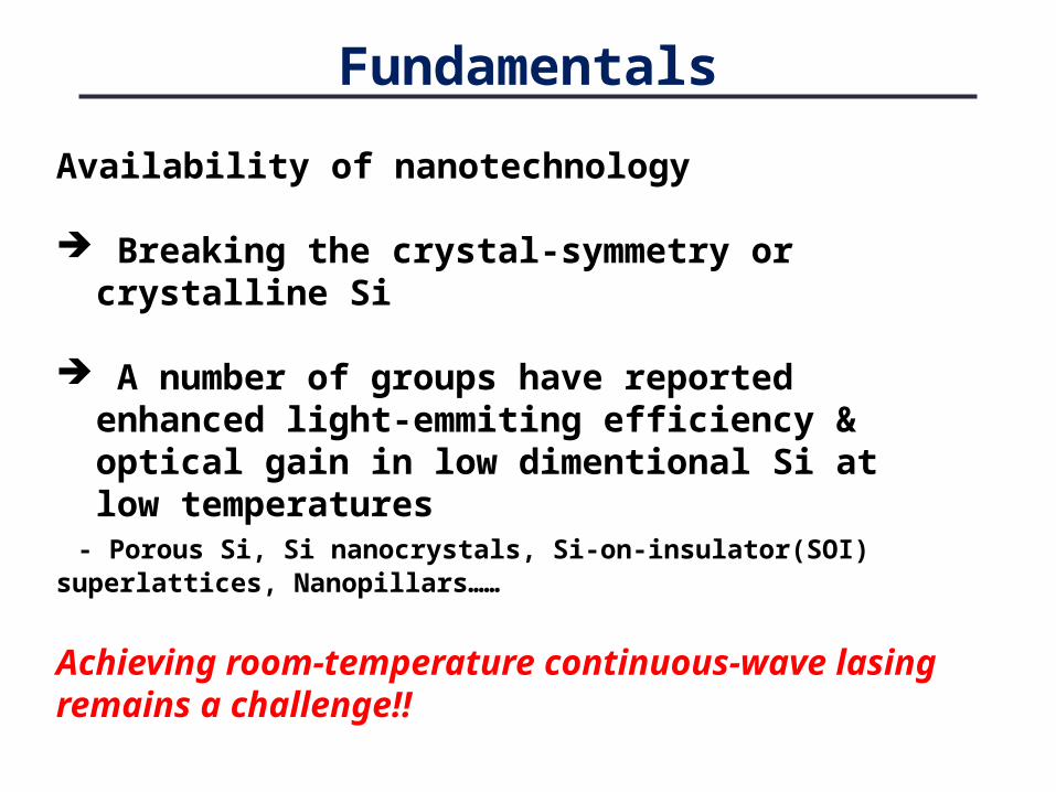
Availability of nanotechnology
Breaking the crystal-symmetry or crystalline Si
A number of groups have reported enhanced light-emmiting efficiency & optical gain in low di-mentional Si at low temperatures
- Porous Si, Si nanocrystals, Si-on-insulator(SOI) superlattices, Nanopillars……
Achieving room-temperature continuous-wave lasing remains a challenge!!

Fundamentals
Advantages of Si for a good substrate
Si wafers are incredibly pure & have low defect density
32 nm CMOS technology is sufficienty advanced to fabricate
Si has a high thermal conductivity, which is a very useful characteristic for an active device substrate
SiO2 serves as a protective layer and a naturally good optical waveguide cladding

Silicon Raman lasersRaman Scattering (or Raman effect)
Inelastic scattering of a photon by an optical phonon A small fraction of the scattered light(≈1/𝟏𝟎𝟕) Raman gain coefficient in Si is around five orders of magni-
tude larger than that in amorphous glass fibres Si waveguide loss is also several orders of magnitude higher than in glass fibres
Two-photon absorption(TPA)
A nonlinear loss mechanism in which two photons combine their energies to boost an electron in the valence band to the conduction band
TPA increases with the number of photons in a waveguide
A limiting factor when using high optical pump powers

Silicon Raman lasers
A high Racetrack ring resonator Cavity
A large bend radius helps to minimize waveguide bending losses
The directional coupler is designed to utilize the pump power efficiently and achieve a low lasing threshold
Overcoming the TPA-induced FCA
TPA-induced FCA nonlinear optical loss can also re-duced by optimizing the p-i-n reverse-biased diode
Silicon Raman lasers nenefit significantly from high spectral purity!!

Epitaxial lasers on silicon
Compared with Si, GaAs and InP have lattice mismatches and thermal expansion coefficient mismatches
Reducing by special surface treatment (strained superlatiices, low-temperature buffers & growth on patterned substrates)
Advanced epitaxial techniques with SiGe & GaSb buffer layers - The realization of GaAs-based CW diode lasers on Si substrates at room temperature
Ge-on-Si(or SiGe-on-Si) epitxial growth - Key photonic components from this material system have demon-strated performances comparable or even better than their III-V coun-terparts in certain aspects

Epitaxial lasers on silicon Germanium has an indirect band structure! Energy gap from the top of the valence band to the momentum-aligned Γ valley is close to the actual band gap!
The tensile strain is able to reduce the energy difference be-tween the Γand L valleys
Strain raises the light-hole band, which increases optical gain for high injection
These techniques have enabled room-temperature direct-bandgap electroluminescence and CW room temperature opti-cally pumped operation of Ge-on-Si lasers
Optically pumped Ge-on-Si laser demonstrating CW operation at room temperature!!
Hybrid silicon lasers
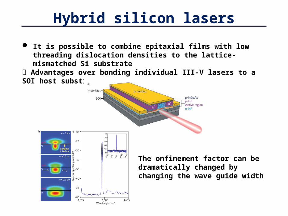
It is possible to combine epitaxial films with low threading disloca-tion densities to the lattice-mismatched Si substrate
Advantages over bonding individual III-V lasers to a SOI host sub-strate
The onfinement factor can be dramat-ically changed by changing the wave guide width

Hybrid silicon lasers
Small size, low power consumption and a short cavity de-sign are all critical for optical interconnects
a schematic of an electrically pumped microring resonator laser, its cross-section SEM image

Hybrid silicon lasers
By lasing inside a compact microdisk III-V cavity and cou-pling to an external Si waveguide, a good overlap between the optical mode and electrical gain results
Schematic of a heterogeneously integrated III-Vmicrodisk laser with a vertically coupled SOI wave guide
Results from combining four devices with diam-eters
Increasing thermal impedance causes laser per-formance to decrease dramatically with smaller diameters A major hurdle in the realization of compact devices

Challenges and opportunities
Opportunities
Optical interconnects could be a possible solution Achieving smaller interconnect delays, lower crosstalk & better re-sistance to electromagnetic interference
Integration with CMOS circuits can provide low cost, integrated con-trol, signals processing and error correction
power consumption must be reduced to 2 pJ bit -1 or lower
Silicon Raman lasers are potentially ideal light sources for a variety of wavelength-sensitive regimes
Raman lasers will be very competitive in size and cost if a pump source can be integrated