
Recent Approaches to Develop High Frequency Power...
17
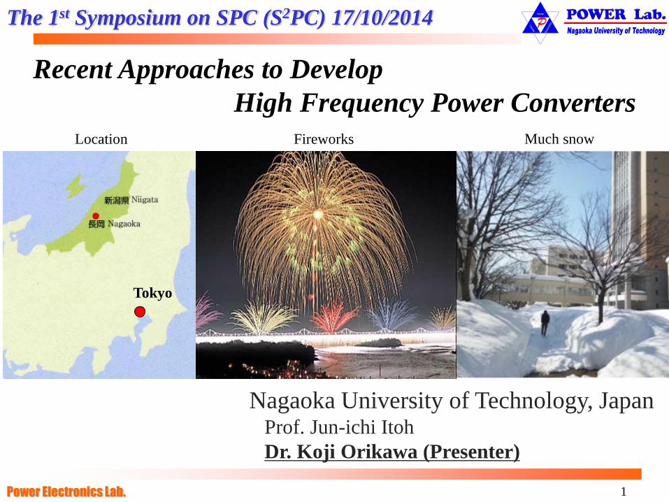
1 Power Electronics Lab. Recent Approaches to Develop High Frequency Power Converters Nagaoka University of Technology, Japan Prof. Jun-ichi Itoh Dr. Koji Orikawa (Presenter) The 1 st Symposium on SPC (S 2 PC) 17/10/2014 Tokyo Location Fireworks Much snow
Transcript of Recent Approaches to Develop High Frequency Power...
1 Power Electronics Lab.
Recent Approaches to Develop
High Frequency Power Converters
Nagaoka University of Technology, Japan Prof. Jun-ichi Itoh
Dr. Koji Orikawa (Presenter)
The 1st Symposium on SPC (S2PC) 17/10/2014
Tokyo
Location Fireworks Much snow

2 Power Electronics Lab. Power Electronics saves the Earth
Power Electronics
Laboratory
Power Electronics
Laboratory
AC to DC
DC to AC
DC
to D
C
AC
to
AC
☆Objectives
☆Research Subjects
・Efficiency improvement & size reduction
of all kinds of power sources.
Four directions of energy conversion “Save the earth”
- Circuit topologies and control
technique
- Optimization of the circuit design
- Development of directional
technology on applications
Members
Associate Professor: Jun-ichi Itoh
PD: 1, Ph. D: 9, M:12, B: 5
=> Total: 28 persons
Power electronics laboratory

3 Power Electronics Lab.
- Motor drive(IM, PMSM)
- Motor design(PM)
- Parameter identification method
- Flywheel energy storage system
-PV inverter, Micro inverter
-Matrix converter for wind turbines
-Multi-level converter
-PFC(“Active buffer”)
- PCB implementation techniques
- Applications of SiC and GaN
- DC-DC converter
- Gate drive circuit
- Wireless power transfer
- Pulse density modulation
Theme Motor
Grid connected inverter
Power decoupling
High switching frequency
converter
etc.
etc.
etc.
Today’s contents
Three Ph. D students
Three Ph. D students
Three Ph. D students
Field of our research

4 Power Electronics Lab.
Fundamental technologies
Applications
DC bus bar analysis in printed circuit boards (PCBs)
High speed & Low power consumption gate drivers
Wireless power transfer for gate drive supplies
of a medium-voltage inverter
Frequency multiplying circuit for MHz output frequency
Wireless charger for electric assisted bicycle using EDLCs
Wireless power transfer with a Rail system
High power density PWM Inverter with wide band-gap devices
Several-Hundred-kHz Single-phase to Commercial Frequency
Three-phase Matrix Converter
Today’s contents
High switching frequency power conversion
High switching frequency ☆Key technology

5 Power Electronics Lab.
GDU
GDU
#1
vin1
vinv
vout1
fsw = 2 MHz
S1 S2
S3 S4
C0
D1-4
C1
#2
····
#3
#6
Proposed method
Transmission
board
Receiver
boards
MV Inv.
Insulation air-gap:50 mm
Only PCBs are used
without solid magnetic cores
Conventional: Special isolated transformers are used
Primary Secondary
- High cost and bulky due to custom designs
Cost reduction & Downsizing of the isolation system
Problems
Multiple wireless power transfer
with transmission coils on PCBs
for multiple gate driver supplies
(6ch)
f = 2MHz
- Reduction of parasitic capacitances is difficult
Multiple gate drive supplies of a medium voltage inverter

6 Power Electronics Lab.
Receiver boards #1~#6
High frequency INV (2MHz)
Series resonance capacitor C0
Transmission coil
Substrate spacing:50 mm
Clearance and creepage distance
are secured
Transmission board #0
50mm
50mm
Diode bridge rectifier
Series resonance capacitor C1
Receiver coil
300mm
15
0m
m
60 mm
50
mm
vin1
C1
vinv
fsw = 2 MHz
S1 S2
S3 S4
C0
Controller
4
48V
System configuration of wireless multiple power transfer

7 Power Electronics Lab.
0
0
0
0
A switching operation on all of receiver boards is confirmed
Enlarged view
Gate drivers are connected
Capacitors are connected
assuming IGBTs 33nF
Inverter output voltage
(Transmitting board)
vinv 50 [V/div]
Input voltage
(Receiving board #1)
vin1 25 [V/div]
Output voltage
(Receiving board #1)
vout1 10 [V/div]
Gate-emitter voltage
(Receiving board #1)
vGE1 20 [V/div]
200[nsec/div]
0
0
0
0
vGE1 50 [V/div]
200 [ns/div] 500 [us/div] 1kHz, ±15V
GDU 1
Transmitting board
48V
#1 vout1
fsw = 2.18 MHz
S1 S2
S3 S4
C0
D1-4
C1
#0
#2
····
#3
#6
C1=70 pF
C0=130 pF
DC
DC
+15V
G0
G1
-15VPWM1
····
GDU 2
G1
GDU 3
GDU 6
Operation waveforms
Experimental results (Operation with gate drivers)

8 Power Electronics Lab.
Miniaturize the EMC filter by using high frequency carrier
Motor drive system using GaN-FET
GaN-FET inverter
Use a PWM rectifier
Sinusoidal input current
High frequency switching
Reduce the ripple current
Advantage of GaN-FET Fast switching
Downsizing
Single stage EMC filter
M
EMC filter PWMRectifier
PWMInverter
GaN-FET GaN-FET
GaN-FET Inverter
Grid Motor
CX CY
LD
LC
GaN-FET Inverter & EMC filter

9 Power Electronics Lab.
Relationship between the carrier frequency
and the total volume of GaN-FET inverter system is evaluated
Conduction noise measurement system
Estimate the conduction noise Volume of the system
EMC
filterLISN
PWM
inverter
PWM
rectifier
RL loadGrid
Stray capacitanceHeat sink
Carrier frequency
Vo
lum
e
EMC filter
Cooling system
GaN-FET inverter system with high frequency carrier
Each volume is calculated based on the simulation results
High frequency noise
Smaller EMC filter
Large switching loss
Larger cooling system
Relationship between volume and carrier frequency

10 Power Electronics Lab.
Power density [kW/dm3]2 3 41
96
95
94
93
92
91
Eff
icie
ncy
[%
] Single stageTwo stages
Three stagesfcarrier=150kHz
fcarrier=600kHz
fcarrier=450kHz
fcarrier=300kHz
High efficiency High power density
EMC filter should be constructed by two stage filter in order to achieve high power density and high efficiency
High power density (fcarrier=300 kHz)
High efficiency(fcarrier=150 kHz)
High efficiency :fcarrier=150 kHz High power density :fcarrier=300 kHz
Relationship between efficiency and power density

11 Power Electronics Lab.
Wireless power transfer
>High frequency
>High efficiency
>Downsizing
Requirements
for HF power source
Applications
Generation of plasma Induction heating Wireless power transfer
Grid 13.56MHz 13.56MHz DC
DC load
HF power
source Rectifier Battery
BatteryCharger
Transmission antenna
Receiver
antenna
Transmission
antenna
Receiver
antenna
(Target)
MHz band high-frequency power converter
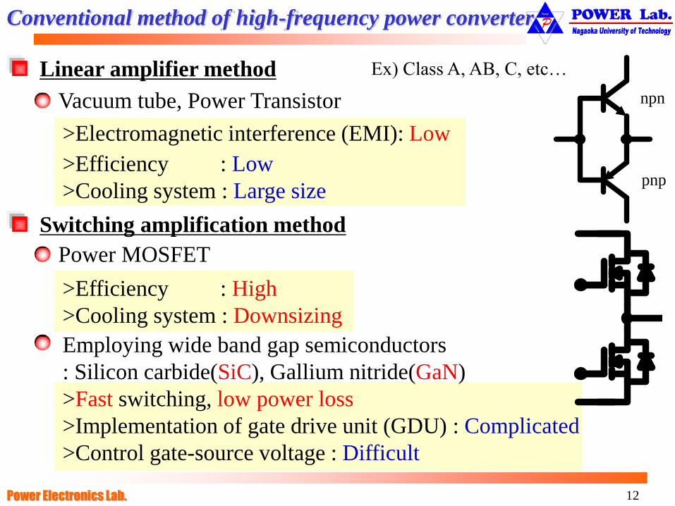
12 Power Electronics Lab.
Vacuum tube, Power Transistor
Linear amplifier method
>Electromagnetic interference (EMI): Low
>Efficiency : Low
>Cooling system : Large size
Switching amplification method
Power MOSFET
>Efficiency : High
>Cooling system : Downsizing
Employing wide band gap semiconductors
: Silicon carbide(SiC), Gallium nitride(GaN)
>Fast switching, low power loss
>Implementation of gate drive unit (GDU) : Complicated
>Control gate-source voltage : Difficult
npn
pnp
Ex) Class A, AB, C, etc…
Conventional method of high-frequency power converter

13 Power Electronics Lab.
Without wide band gap semiconductors,
only conventional Si devices are used
Simple method
>Conventional GDU can be used
Frequency multiplying method is adopted
High output frequency over
switching frequency
Concept
Low
switching
frequency
High
efficiency
Simple
VDCv
uo
VDC
2
VDC
2
wx
y
Vout
Spu
Snu
Spv
Snv
Spw
Snw
Spx
Snx
Spy
Sny
Vuo
Iu
Concept of the proposed circuit and purpose of this study

14 Power Electronics Lab.
VDCv
uo
VDC
2
VDC
2
wx
y
Vout
Spu
Snu
Spv
Snv
Spw
Snw
Spx
Snx
Spy
Sny
Vuo
Iu
1. Multi-phase inverter
Square wave drive
2. Multi-core transformer
Primary : Parallel connection
Secondary: Series connection
1. Multiphase inverter with square wave drive using shifted gate signal
2. Multicore transformer is adopted
Sum of the inverter output voltage can achieve high output frequency
fout = N*fsw Ex.) fout = 2.5 MHz, N = 5 fout = 500 kHz
Output
voltage
U-phase
voltage
V-phase
voltage
W-phase
voltage
X-phase
voltage
Y-phase
voltage
72 deg.
72 deg.
72 deg.
72 deg.
VDC/2
-VDC/2
VDC/2
-VDC/2
VDC/2
-VDC/2
VDC/2
-VDC/2
VDC/2
-VDC/2
VDC/2
-VDC/2
Tsw
Tsw/5
0
0
0
0
0
0
Vuo
Vvo
Vwo
Vxo
Vyo
Vout
Proposed circuit –Frequency multiplying method -

15 Power Electronics Lab.
Applying series resonance using resonance capacitance
VDC
o Vout
Vuo
Sp
u
Sn
u
Sp
u
Sn
u
Sn
u
Sn
u
Spy
Sny
VDC
2
VDC
2 Vvo
Vwo
Vxo
Vyo
uvwxy
Leakage
inductance
Resonance
capacitor Multi-phase inverter
Sinusoidal
voltage
A resonance capacitance is connected to the secondary side of multi-
core transformer
Leakage inductance is effectively used for sinusoidal output voltage

16 Power Electronics Lab.
0 100 200 300 400 500 600
10
20
30
40
50
60
Lo
ad v
olt
age
Vlo
ad [
V] (a)
Resonance capacitance Cr [pF]
Rload: 100 W
Rload: 33 W Rload: 50 W
(b)
400 (ns)
0
0
0
0
U phase voltage
Vuo
U phase current
Iu
(100V/div)
(2A/div)Load voltage
Vload
(100V/div)Output current
Iout
(1A/div)
400 (ns)
0
0
0
0
U phase voltage
Vuo
U phase current
Iu
(100V/div)
(2A/div)Output voltage
Vout
(100V/div)Output current
Iout
(1A/div)
rms value
Load voltage and current
Almost sinusoidal
waveform
High output
Load resistance: Small
Quality factor for resonance: Large
> Output voltage: Decreased
Output voltage is changed by
resonance capacitance value
(a) Rload: 50W (Cr:100pF)
(b) Rload: 33W (Cr:100pF)
Experimental results (Series resonance, fout=2.5MHz)
Power Electronics Lab. 17
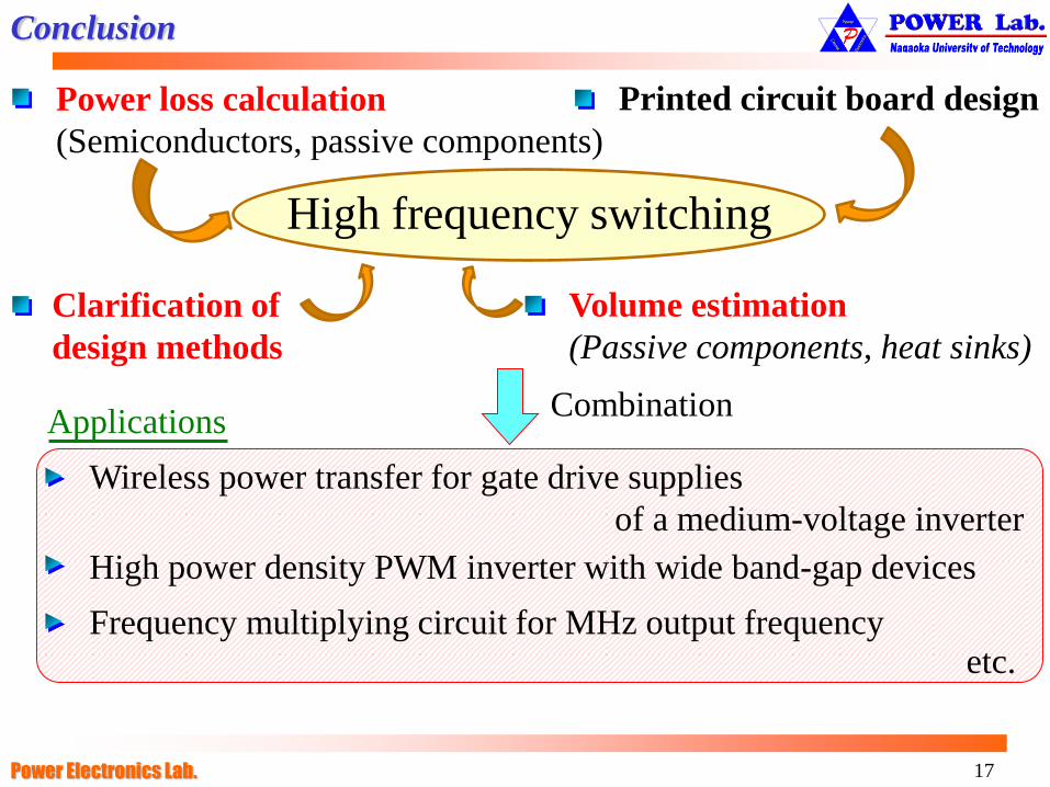
High frequency switching
Power loss calculation
(Semiconductors, passive components)
Volume estimation
(Passive components, heat sinks)
Printed circuit board design
Combination
Wireless power transfer for gate drive supplies
of a medium-voltage inverter
Frequency multiplying circuit for MHz output frequency
High power density PWM inverter with wide band-gap devices
etc.
Applications
Clarification of
design methods
Conclusion


