![Incremental metal-powder solidification by localized ...jerby/81.pdf · spark plasma sintering (SPS) process [21] demonstrates sinter-ing, consolidation and crystal growth by spark](https://static.fdocuments.net/doc/165x107/60b53db6a20dbf1ef559b6c2/incremental-metal-powder-solidification-by-localized-jerby81pdf-spark-plasma.jpg)
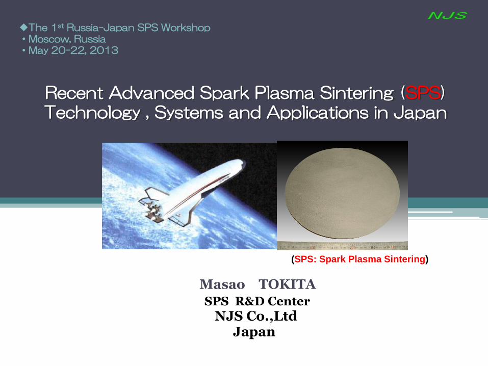
Recent Advanced Spark Plasma Sintering (SPS) Technology , Systems...
65
SPSの最近の研究・開発動向 ―放電プラズマ焼結と商品開発― The 1 st Russia-Japan SPS Workshop ・Moscow, Russia ・May 20-22, 2013 (SPS: Spark Plasma Sintering) Recent Advanced Spark Plasma Sintering ( SPS) Technology , Systems and Applications in Japan Masao TOKITA SPS R&D Center NJS Co.,Ltd Japan
-
Upload
truongphuc -
Category
Documents
-
view
213 -
download
0
Transcript of Recent Advanced Spark Plasma Sintering (SPS) Technology , Systems...
SPSの最近の研究・開発動向 ―放電プラズマ焼結と商品開発―
The 1st Russia-Japan SPS Workshop ・Moscow, Russia ・May 20-22, 2013
(SPS: Spark Plasma Sintering)
Recent Advanced Spark Plasma Sintering (SPS) Technology , Systems and Applications in Japan
Masao TOKITA SPS R&D Center
NJS Co.,Ltd Japan

CONTENTS
● Introduction of Recent SPS Technology
● Demands from Industries on SPS
● Advanced SPS Systems
● Large Scale Ceramics by SPS
● Outlook & Summary

Lockheed Co.(USA) bought the patent in 1968
Kanagawa Science Park (KSP) and ex. JAPAX INC building at left
The 1 st Generation SPS
SPS Technology was originally born in Japan
Right : Dr. K.Inoue (The first SPS Inventor/president of JAPAX)
Left : Mr. K.Okazaki (The first president of JAPAX INC.)

Russia - Japan
( U.S.S.R )
Dr. B.R. Lazarenko & Dr. N. I. Lazarenko of U.S.S.R. in 1943
EDM invented in Russia by Dr. Lazarenko
EDM also invented in Japan by Dr. K. Inoue
● Electrical Discharge Machine ( Electrospark Machining )
= Founder of EDM Technology
Wire-Cut EDM
Ram-type EDM
Spark Sintering
ECM ECG
ECB ECDM SPS :
Spark Plasma Sintering
Spark Forming

■Progress of SPS Technology
Nano, Porous,Thin film
Reaction, Synthesis
Composite
Ultra-Vacuum
SPS Chemistry
Kinetic Window
Electro-migration
Re
se
arc
h &
D
eve
lopm
ent
Rapid High-density
Homogeneity
Fine micro-structure
Low temperature
Amorphous

Increasing Use of SPS Technology
in Japan
0
5
10
15
20
25
30
35
40
45
1990 1991 1992 1993 1994 1995 1996 1997 1998 1999 2000 2001 2002 2003 2004 2005 2006 2007
Powder & Powder Metlgy. Spring
Powder & Powder Metlgy. Autumn
Ceramics Japan Spring
Ceramics Japan Autumn
Japan Inst.Metals Spring
Japan Inst.Metals Autumn
Nu
mb
er
of
Pre
se
nta
tio
ns
Number of presentations on the SPS introduced at major advanced
materials conferences from 1990 to 2007
Private Enterprise 0
50
100
150
200
250
1993
1994
1995
1996
1997
1998
1999
2000
2001
2002
2003
2004
2005
2006
2007
/Mar
ch

As of 2010, more than 550 units of SPS machine systems installed in total
in 2005
Figure 3. Increasing use of the SPS machines in the world (SPS units produced & installed 1990-2010)
SPS Job-shop center in Japan (left/3MN right/200KN) φ300mm large Al2O3 SPSed compact(Relative density:98%)
“Advanced Ceramics Handbook 2nd Edition”
American Ceramics Society, Published in 2013, Chapter 11.2.3 “SPS”
Increasing Use of SPS Technology
♦2012(estimated)
◇SPS TOTAL:
650-700 units
◇Manufacturers:
14 Companies
In the World

▲Max Planck
Institute,
Dresden, Germany
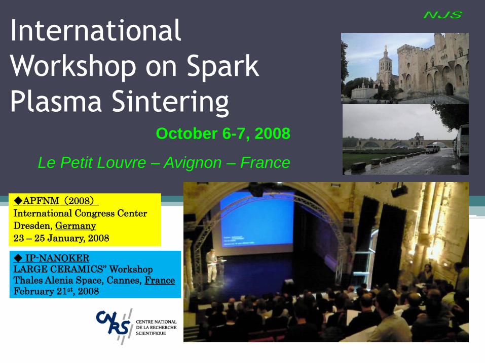
International
Workshop on Spark
Plasma Sintering October 6-7, 2008
Le Petit Louvre – Avignon – France
◆APFNM(2008)
International Congress Center
Dresden, Germany
23 – 25 January, 2008
◆ IP-NANOKER LARGE CERAMICS” Workshop Thales Alenia Space, Cannes, France February 21st, 2008

PacRim7 held in Shanghai, China 11-14 Nov. 2007 SPS session “Spark Plasma Sintering Synthesis and Processing of Materials”

2010-2012 Pulse Energizing Processes(SPS)
① 2011 Autumn SERVO METAL FORUM
② 2012 Winter
SERVO METALRORUM
③ 2010 July SPS BOOK 28Papers/8Chapters
Total・343 Pages Authors・28 Publisher:[TIC Inc.
④「Materials Integration」(TIC Inc.)
2010, July/Aug/Oct/Nov SPS Special Edition
● Annual Symposium “SPS FORUM of Japan”
2011/ November 16th in Sendai, Tohoku University
●2012 / June STAC-6 Int. Sympo (Yokohama) SPS Special Session
●2012 / October PM2012 Int. Congress (Yokohama) SPS Special Session
●2012 / December ”17th SPS FORUM of Japan”, Tohoku University
Recent SPS Activities in Japan

• Sintering
• Sinter-Bonding & Joining
• Surface Treatment
• Synthesis Nano-Phase
Materials
Thermo-Electric
Materials
Bio-Materials
Functionally Graded
Materials (FGMs)
Versatile Process & Large Number
of Potential Applications
Advanced Ceramic
Materials
and others

Pure Nano SiC (30nm → 100nm)
R.D : 99.4%
mHV : 2380
Transparent ceramics
Suitable materials for SPS processing
Oxides
Carbides
Nitrides
Borides
Flourides
Classification Materials for SPS processing
Cr, Mo, Sn, Ti, W, Be
SiC, B4C, TaC, TiC, WC, ZrC, VC
Metals
Fe, Cu, Al, Au, Ag, Ni Virtually any metals possible
Ceramics
Al2O3, Mulite, ZrO2, MgO, SiO2, TiO2, HfO2
TiB2, HfB2, LaB6, ZrB2, VB2
LiF, CaF2, MgF2
Si3N4, TaN, TiN, AlN, ZrN, VN
NbCo, NbAl, LaBaCuSO4, Sm2Co17
Organic materials (polyimide, etc.), compositematerialsOther materials
SUS+WC/Co, BN+Fe, WC+Co+Fe
Intermetaliccompounds
TiAl, MoSi2, Si3Zr5, NiAl
Cermets
Si3N4+Ni, Al2O3+Ni, ZrO2+Ni
Al2O3+TiC, SUS+ZrO2, Al2O3+SUS
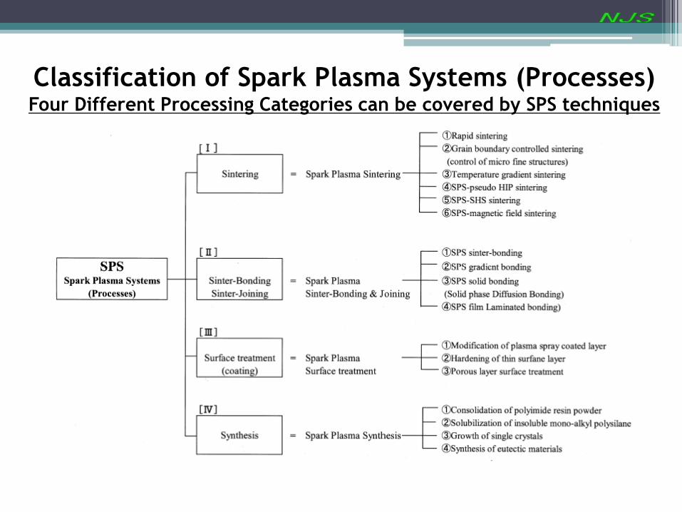
Classification of Spark Plasma Systems (Processes) Four Different Processing Categories can be covered by SPS techniques

Recent Demands for SPS form Industries
Fully Automated Machine Systems
More Complex Shape Product
Higher Functionality
Hybrid materials
Thinner materials
Finer & Smaller Sized Products
Nano-crystalline materials
Finer micro structural materials
Porous materials
Higher Reliability & Safety
High Value Added Products
Multi-use, Small-Medium scale Production
Highly Dense materials
Highly Homogeneous materials
High Reproducibility ( Repeatability )
Larger Sized Products
Thicker materials
Single Crystal materials
General Purpose Sintered Products
Manual type Simple &
Low cost machine systems
SPS
EX) 10 K ~ 30 K(70K~100K) pieces/month
General purpose Mass, Large scale Production
Composite materials
3-D Near-Net/Net shape Forming

SPS system configuration
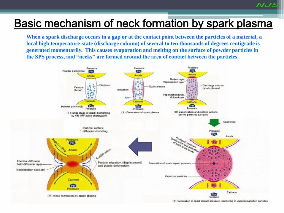
Basic mechanism of neck formation by spark plasma When a spark discharge occurs in a gap or at the contact point between the particles of a material, a
local high temperature-state (discharge column) of several to ten thousands of degrees centigrade is
generated momentarily. This causes evaporation and melting on the surface of powder particles in
the SPS process, and “necks” are formed around the area of contact between the particles.
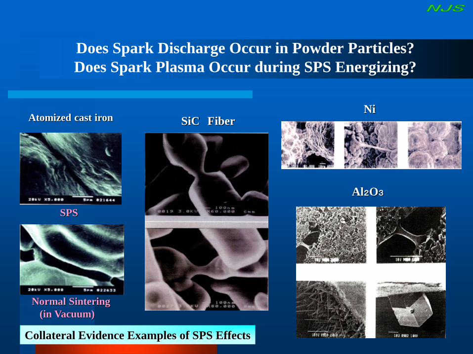
Does Spark Discharge Occur in Powder Particles?
Does Spark Plasma Occur during SPS Energizing?
Collateral Evidence Examples of SPS Effects
Al2O3
Ni Atomized cast iron
SPS
Normal Sintering
(in Vacuum)
SiC Fiber

PROCESSING
(SOFTWARE)
SYSTEM
(HARDWARE)
POWDER
MATERIALS
Concept of SPS technology development = “Trinity system” of
Hardware, Software and Powder Materials
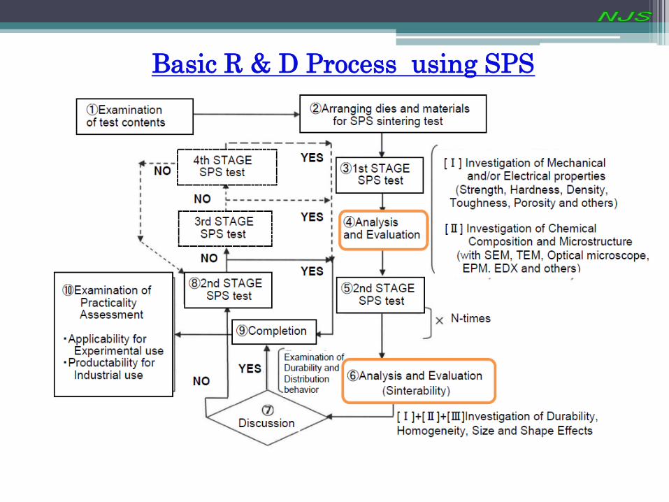
Basic R & D Process using SPS
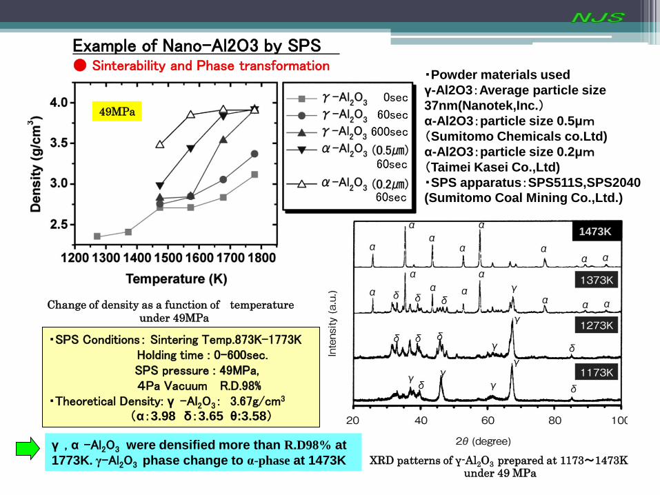
Example of Nano-Al2O3 by SPS
XRD patterns of γ-Al2O3 prepared at 1173~1473K under 49 MPa
・Powder materials used
γ-Al2O3:Average particle size
37nm(Nanotek,Inc.)
α-Al2O3:particle size 0.5μm(Sumitomo Chemicals co.Ltd)
α-Al2O3:particle size 0.2μm
(Taimei Kasei Co.,Ltd)
・SPS apparatus:SPS511S,SPS2040 (Sumitomo Coal Mining Co.,Ltd.)
1473K
Change of density as a function of temperature
under 49MPa
● Sinterability and Phase transformation
・SPS Conditions: Sintering Temp.873K-1773K Holding time : 0-600sec. SPS pressure : 49MPa, 4Pa Vacuum R.D.98% ・Theoretical Density: γ -Al2O3: 3.67g/cm3
(α:3.98 δ:3.65 θ:3.58)
γ , α -Al2O3 were densified more than R.D98% at
1773K. γ-Al2O3 phase change to α-phase at 1473K
49MPa

Change of density as a function of temperature at 690MPa
SEM micrograph of γ-Al2O3
and α-Al2O3 (0.2μm,0.5μm)
prepared at 1773K under
49 MPa for 60s.
FE-SEM micrograph of γ-
Al2O3 prepared at 973~1173K
under 690 MPa
≒80nm
≒150-300nm
≒300-600nm
R.D98%
R.D85%
Density decreased due to γ-phase change to δ and θ-phase
R.D79%
α
α
690 MPa
XRD patterns of
γ-Al2O3 prepared
a 973~1173K under
690 MPa
γ-Al2O3 prepared by SPS
α-Phase transformation occurred at 1173K under pressure of 690MPa . Approx.300K lower than 49MPa of 1473K.
Grain growth was minimized
Pressure Effects in SPS <49MPa Vs 690MPa> Phase and Grain Growth Behavior
γ- -Al2O3 (γ ,δ, θ) 690 MPa
37nm
1773K,49MPa
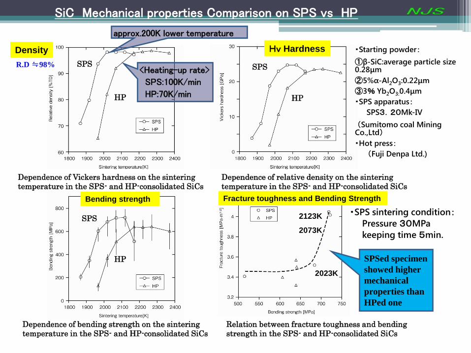
SiC Mechanical properties Comparison on SPS vs HP sintered compact
Dependence of relative density on the sintering
temperature in the SPS- and HP-consolidated SiCs
Dependence of Vickers hardness on the sintering
temperature in the SPS- and HP-consolidated SiCs
Dependence of bending strength on the sintering
temperature in the SPS- and HP-consolidated SiCs
Relation between fracture toughness and bending
strength in the SPS- and HP-consolidated SiCs
・Starting powder:
①β-SiC:average particle size 0.28μm
②5%α-Al2O3:0.22μm
③3% Yb2O3:0.4μm
・SPS apparatus:
SPS3.20Mk-IV
(Sumitomo coal Mining Co.,Ltd)
・Hot press:
(Fuji Denpa Ltd.)
<Heating-up rate>
SPS:100K/min
HP:70K/min
・SPS sintering condition:
Pressure 30MPa
keeping time 5min.
SPS
HP
SPS
HP
HP
SPS
R.D ≒98%
approx.200K lower temperature
2123K
2073K
2023K
SPSed specimen
showed higher
mechanical
properties than
HPed one
Bending strength Fracture toughness and Bending Strength
Hv Hardness Density

From XRD and Raman scattering analysis, it is suggested that disordered cubic structure (3C-type) of SiC can be preserved in the SPS consolidation, and the scarce detection of Yb3Al5O12 phase suggests the existence of oxide additives in amorphous-like state.
XRD patterns obtained from raw powder, SPS- and HP- SiCs
Raman scattering spectra obtained from
raw powder, SPS- and HP-consolidated SiCs
1 m
mm
1m
m
SPS/ 2073K 30MPa HP 2273K 30MPa
SPS sintered compact shows larger grain size than HP compact, however the bending strength and fracture toughness are higher than HP sintered compact. ⇒ SPS can improve those mechanical properties. Grain boundary of crystallographic behavior is different
SiC

(By Prof. Munir etal. Of California University )

SPS Technology Topics (Especially from overseas SPS researchers)
● One of the distinctive phenomenon of SPS is “Kinetic Window”. There is an obvious difference in powder particle size 100-200nm and under 50nm (20-30nm). Rapid grain growth occurs in a few dozen degrees of sintering temperature difference. ・・・・・ Stockholm Univ. /Prof. M. Nygren, ( NJS/Dr.M.Tokita )
● Actual temp. difference in sintering temp. measurement seems significant, but not so practical. ・・・・・ Max-Plank-Institut /Dr. Y. Grin Stockholm Univ. /Prof. Nygren , ( NJS/Dr.M.Tokita )
● SPS is recognized as a Reaction Synthesis (Sintering) → Need New Concept. ・・・・・ CNRS/Dr.J.Galy, Univ. of Burgundy / Prof. F. Bernard Univ. of California-Davis / Prof. Z.A. Munir
Max-Plank-Institut /Dr. Y. Grin, ( NJS/Dr.M.Tokita ) Stockholm Univ. /Prof. M. Nygren
● Continuous researches on differences between AC/DC and also relation between Heating Rate, Densification, Grain Growth and Pulse Energizing Effect. ・・・・・ Univ. of California-Davis, Wuhan Univ. of Technology
Univ. of Burgundy Stockholm Univ. etc. ( NJS/Dr.M.Tokita )
● SPS is most effective Sintering & Synthesis Method for Nano/Nano-Composite Materials. ・・・・・ Shanghai Institute of Ceramics / Prof. L. Chen Tsing Hua Univ. etc. ( NJS/Dr.M.Tokita ) Many other researchers from every country

Wave Form of Thyristor-type SPS Pulse Generator (patented) < developed, manufactured and measured by Sumitomo/SPSS since 1989 >
ON-Time setting: 1 (3.3ms) ON-Time setting: 99 (326.7ms) OFF-Time setting: 1 (3.3ms) OFF-Time setting: 9 (29.7ms)
ON-Time setting: 12 (39.6ms) OFF-Time setting: 2 (6.6ms)
Wave Form of Inverter-type SPS Pulse Generator (developed, manufactured and measured by Sumitomo/SPSS in 1996-98)
ON-time: 10ms OFF-time: 30ms ON-time: 30ms
OFF-time: 10ms
ON-time: 90ms OFF-time: 10ms
(IGBT/PWM Control system)

Different type of SPS machine systems Developed in Japan
[Ⅰ] Multi Head System [Ⅱ] Batch System [Ⅲ] Tunnel –type System [Ⅳ] Rotary-type System [Ⅴ] Shuttle-type System
Full Automatic SPS System (Tunnel-type)
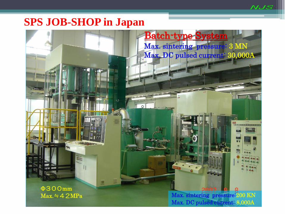
SPS JOB-SHOP in Japan
Batch-type System Max. sintering pressure: 3 MN
Max. DC pulsed current: 30,000A
Max. sintering pressure:200 KN
Max. DC pulsed current: 8,000A
Φ300mm
Max.≒42MPa

Disk-shape 300-350mm in diameter of metallic sputtering target fabricated by SPS
01234
56789
SPS HP/HIP
Time
Comparison of sintering time
between SPS and HP/HIP methods
• SPS Sintering Temperature: 1373~1473K
• Relative Density: 99~100%
Example of Large-sized Product in Materials Industry
Other examples) CrB2, CrB, SiC, SiO2, Ta2O5, ITO
BaTiO3, PbTiO3, TiN, TiAl, Ti-Al-Si
Mg2Si, Ru, RuCo, NiCr, Ti-Ta

WC/Co Diamond Cutting Blade by SPS
Sintering Powder Material (or Green body)
Outer Diameter Φ 100/150mm
Inner Diameter Φ 40/60mm
Thickness 0.35/0.4mm
SPS sintering temp. 1473 ~1523K
Sintering Pressure 40 ~50MPa
Relative Density 99 ~100%
Young Modules 500 ~580GPa
Flatness <±20μ m
Graphite Spacer
Multi Layers: n = 5~20
possible
Example of Batch Production Method in Tools Industry
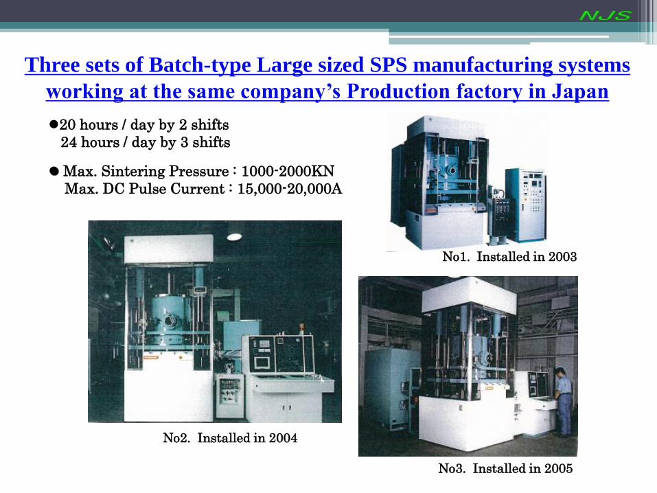
Three sets of Batch-type Large sized SPS manufacturing systems
working at the same company’s Production factory in Japan
No3. Installed in 2005
No2. Installed in 2004
20 hours / day by 2 shifts
24 hours / day by 3 shifts
Max. Sintering Pressure : 1000-2000KN
Max. DC Pulse Current : 15,000-20,000A
No1. Installed in 2003

Hybrid System - Tunnel-type Automatic SPS
Manufacturing systems
Inlet
Vacuum Exhaust
Pre-Heating
SPS Sintering
Cooling-1
Cooling-2 /Air Introduction
Outlet
Developed & Installed in 2001
FGM by SPS system
5-Chamber system
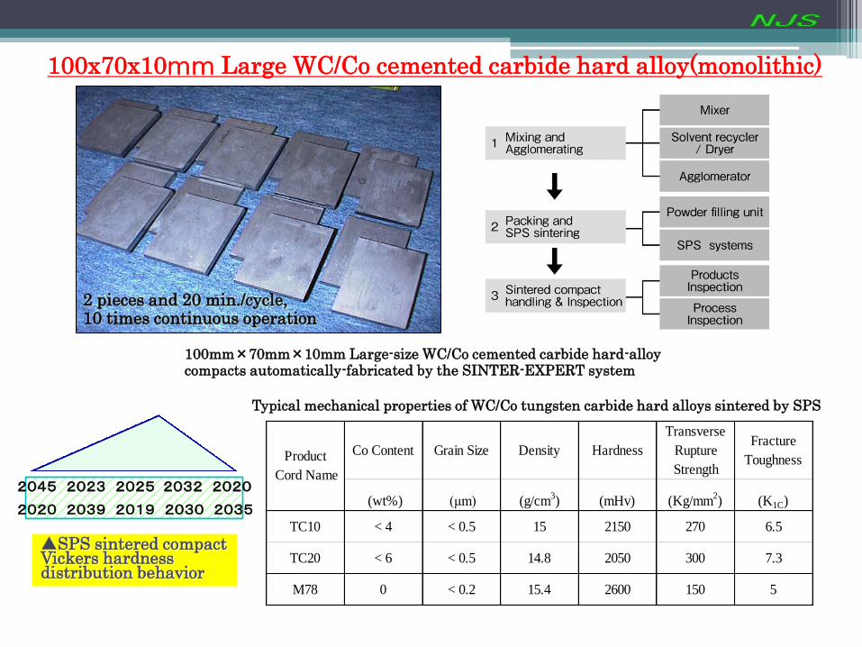
100mm×70mm×10mm Large-size WC/Co cemented carbide hard-alloy compacts automatically-fabricated by the SINTER-EXPERT system
Co Content Grain Size Density Hardness
Transverse
Rupture
Strength
Fracture
Toughness
(wt%) (μm) (g/cm3) (mHv) (Kg/mm
2) (K1C)
TC10 < 4 < 0.5 15 2150 270 6.5
TC20 < 6 < 0.5 14.8 2050 300 7.3
M78 0 < 0.2 15.4 2600 150 5
Product
Cord Name
Typical mechanical properties of WC/Co tungsten carbide hard alloys sintered by SPS
2045 2023 2025 2032 2020
2020 2039 2019 2030 2035
▲SPS sintered compact Vickers hardness distribution behavior
100x70x10mm Large WC/Co cemented carbide hard alloy(monolithic)
2 pieces and 20 min./cycle, 10 times continuous operation
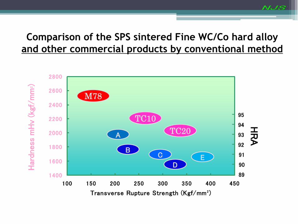
Comparison of the SPS sintered Fine WC/Co hard alloy
and other commercial products by conventional method
1400
1600
1800
2000
2200
2400
2600
2800
100 150 200 250 300 350 400 450
Transverse Rupture Strength (Kgf/mm2)
M78
TC10
TC20 A
B C
D E
Har
dnes
s m
Hv
(kgf
/m
m2 )
HR
A
95
94
89
91
90
92
93

Nano-WC :Examples of Aspheric Glass Lens Molds

Binderless Pure-WC Oxidation Resistance
Comparing weight loss changes of surface area per specimens after 700℃×10hrs heating in atmospheric furnace
0.050
0.055
0.060
0.065
0.070
0.075
0.080
0.085
0.090
M78 A company B company
Super Hard Alloy Materials
Am
ou
nt
of
Oxid
ati
on
(g/c
m2)
SPSed pure-WC
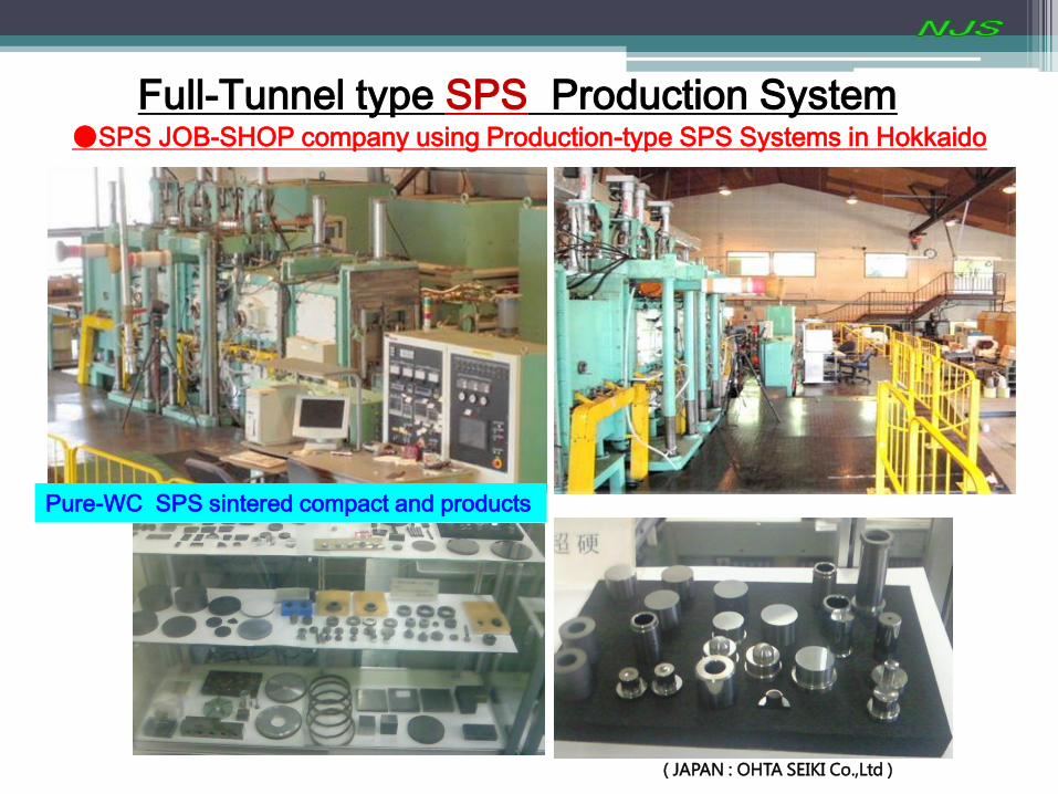
Full-Tunnel type SPS Production System ●SPS JOB-SHOP company using Production-type SPS Systems in Hokkaido
Pure-WC SPS sintered compact and products
( JAPAN : OHTA SEIKI Co.,Ltd )

Largest in the World
Semi-Tunnel type SPS Production System
”The 5th Generation-type”
JAPAN/ SINER LAND INC. (Box type Chamber/Auto Feeding System )
➢Max.pressure:
600tonf(6MN)
➢ Max. pulse current:
40,000A
➢ 3-Chamber system: ・Pre-heating stage
・SPS sintering stage
・Cooling stage ➢ Invertor Pulse Generator
(Φ300mm:Max.85MPa)

Semi-Tunnel type SPS Production System ● World s Largest SPS System 600 tonf(6MN ) / 40,000A
Pre-HEATING SPS SINTERING COOLING
IN-LET OUT-LET
JAPAN/SINER LAND INC.

< Large size Production -type SPS System>
● Max. Pressure:3 ~ 10 MN (300~1,000 tonf)
● Max. Pulse Current Out-put:20,000~40,000 A
(JPX-300G-Ⅲ:3MN)
▲ 300mm Al2O3
(RD:98%)
”The 5th Generation”
【Features】
・Flexible system
・Additional Multi-chamber system is available
for an automated production with a special conveyer.
・The latest hardware ✔ Specially designed ON-OFF DC Pulse Generator
for High efficiency and Energy-saving
✔ Newly developed JPX Touch Panel operation screens
✔ High cooling performance
・Safety and reliable long-run operation
・Easy maintenance

OFF Panel
LABOX Touch Panel System and Vacuum Chamber Model:LABOX-1575(150KN/5000~10000A)
”The 5th Generation” ● One Box “ALL-IN ONE”・AC Servo Motor System
Medium size LABOX SPS System(LABOXTM M-series)

Custom-type Small size LABOX SPS System (C-series)
● With Glove Box &Turbo molecular Vacuum Pump
MODEL:LABOX-125GH JAPAN/SINER LAND INC.
”The 5th Generation”
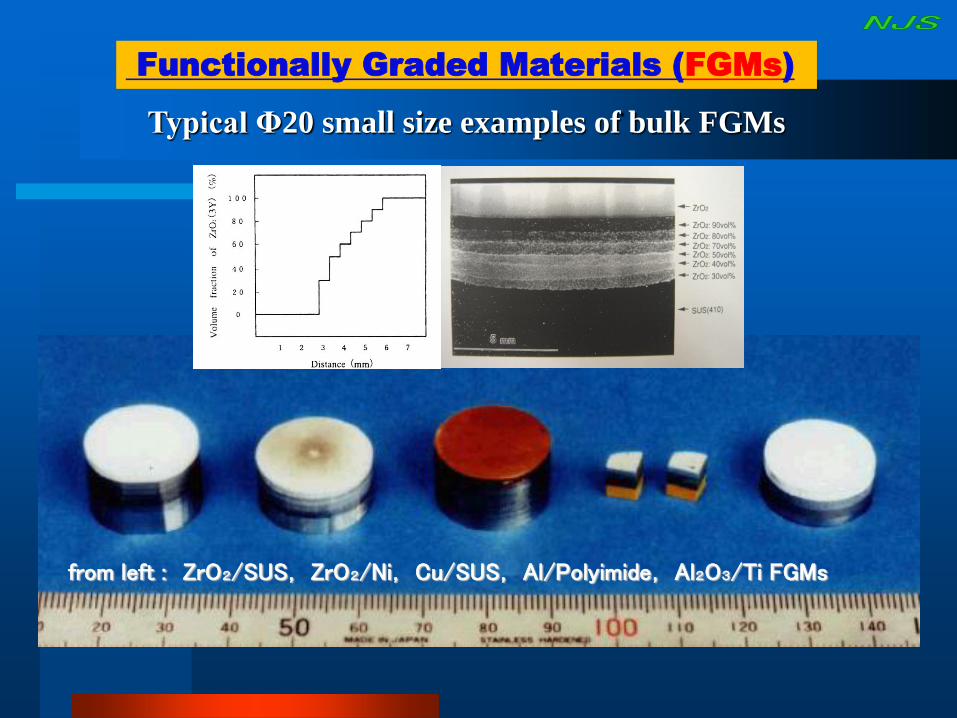
Typical Φ20 small size examples of bulk FGMs
from left : ZrO2/SUS, ZrO2/Ni, Cu/SUS, Al/Polyimide, Al2O3/Ti FGMs
Functionally Graded Materials (FGMs)

Φ20mm Cu/Thermosetting-Polyimide FGM Φ20mm Al/Thermosetting-Polyimide FGM
Examples of Polymer- Metal system FGMs

Scaling-up & Homogenization Functionally Graded Materials of ZrO2 (3Y)/Stainless Steel FGM
55 mm
20 mm 55
mm
40 mm
Φ20mm Φ30mm Φ50mm Φ80mm
Temperature
gradient die
(NEDO Project)

Example of Perpendicular type 3-D formed Φ80mm Large-size ZrO2 (3Y)/ Ti / Ti-Al system FGM
50%

5
7
20
8
Co WC
Large FGM block was machined by Wire-cut EDM and Grinding machines
Applied for Press stamping Dies, and the life time is 7~8 times longer than conventional products
WC0.5μ m-6%Co
WC0.5μ m-4%Co
WC3.5μ m-15%Co
WC5.0μ m-20%Co
Co W1μ m
[Scaling-up II]
Square-Shaped Large-Size of 100mmx100mmx40~60mm WC/Co Cemented Carbide Hard-Alloy FGM
▲ Profile of micro hardness on Co content
graded cemented carbide by SPS
100x100x40mm large-size WC/Co FGM fabricated by SPS
▲SEM micrograph (left) and EPMA analyses (center & right) of
100x70x20mm 4-layered WC/Co FGM

Examples of WC/Co, WC/Co/Ni System FGMs for Press Stamping Dies & Punches
Wire-Cut Electrical
Discharge Machining on
FGM

Optical microphotograph and Vickers hardness
distribution behavior of Weldable WC/Ni system
FGM tile
TIG Welding using WC/Ni FGM and FGM
Screw products (lower left) and FGM built-
in Extruding machine (lower right)
Application Example for Screw of Extruding Machine Weldable WC/Ni FGM (Ni10%,20%,30wt% 3 layers)
Lifetime of Conventional Screw:800~1000 Hours → WC/Ni FGM Screw:more than 3000 Hours
Desulfurization Pellets Operation of Pellet Extrusion
Vickers Hardness Comparison
PLS/ HP/ HIP and SPS on Al2O3
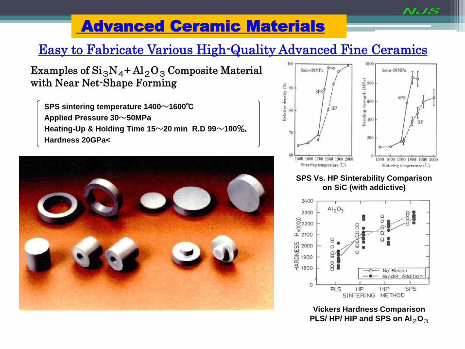
Easy to Fabricate Various High-Quality Advanced Fine Ceramics
SPS sintering temperature 1400~1600℃
Applied Pressure 30~50MPa
Heating-Up & Holding Time 15~20 min R.D 99~100%,
Hardness 20GPa<
Examples of Si3N4+ Al2O3 Composite Material
with Near Net-Shape Forming
SPS Vs. HP Sinterability Comparison
on SiC (with addictive)
Advanced Ceramic Materials

NANO-SiC Compacts Sintered by SPS at 1700 ℃
Rel
ati
ve
Den
sity
[%]
Sintering Temperature[℃]
TEM Microphotographs
(The average diameter of the starting MA powder materials aprox. 30nm)
Nano SiC Porus
RD: 62.5%
Holding time : 0min
Nano SiC densematerials
RD: 97.7%
Holding time : 10min The relationship between MA time and
Si, C Powder XRD (X-Ray Diffraction)
Str
ength
[a.u
.]
Str
ength
[a.u
.]

GeneralCommercialProducts
SPS Sintered Nozzle
Advantage of SPS sintered
Nozzle
Vickers Hardness
(Hv)900-1100 2100-2200 High-Hardness
RelativeDensity (%) 91 100 High-Density
Surface Rough Mirrored surface
Mirror finished surface by
Near Net Shape
Lifetime 1 day 10 days 10 times longer Lifetime
Comparison between SPS sintered nozzle and general commercial products
3-Dimensional complex shape (Outer-Tapered type) of Al2O3 Blasting Nozzle by SPS
Material: Al2O3
Dimensions: Length: 60mm Outer diameter (Tapered):
Φ30/15mm Inner diameter (Straight): Φ6mm

Material: Al2O3
Material: pure-WC(no addtives) Material: SiC (with addtives)
Dimensions: φ200x10mm
Dimensions: φ100x16~50mm Dimensions: φ150x20mm
R.D: 99-100%
R.D:99-100% R.D: 99-100%
Material: Al2O3
Dimensions: φ300x6mm
Examples of Large-size Ceramics Fabricated by SPS

0
200
400
600
800
1000
1200
0 10 20 30 40 50 60 70 80
左 正面 右 奥 正面‐右(放射温度計)
54min. Keep Start
74Min. Energizing End
SPS Temperature Distribution Behavior TEST-II (φ 200mm: Example of abnormal SPS machine conditions)
T.C Rear side
T.C Front
T.C Right
T.C Left
Chamber Front
T.R.M. Front-Right
300 tonf Temp. Distribution TEST-II Settings R F L Bk F-R(T.R.M)
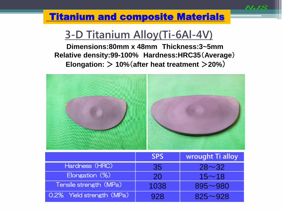
3-D Titanium Alloy(Ti-6Al-4V) Dimensions:80mm x 48mm Thickness:3~5mm
Relative density:99-100% Hardness:HRC35(Average)
Elongation: > 10%(after heat treatment >20%)
SPS wrought Ti alloy
Hardness(HRC) 35 28~32 Elongation(%) 20 15~18
Tensile strength(MPa) 1038 895~980 0.2% Yield strength(MPa) 928 825~928
Titanium and composite Materials
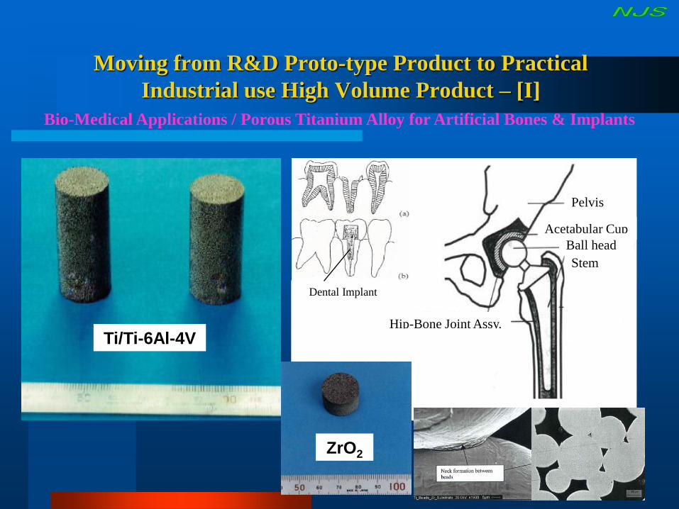
Moving from R&D Proto-type Product to Practical
Industrial use High Volume Product – [I]
Bio-Medical Applications / Porous Titanium Alloy for Artificial Bones & Implants
Ti/Ti-6Al-4V
ZrO2
Dental Implant
Hip-Bone Joint Assy.
Pelvis
Acetabular Cup
Stem
Ball head

Rapidly
solidified
powder
Super
plastic
forming
Powder
Consolidation
Component
Fine micro-structure < 1 um
Low temperature sintering
High strain rate > 10-2s-1
From R&D Product to Practical Industrial use High Volume Product – [II]
Fabricating process for high performance aluminum alloy components
Nano crystalline
particle used
Nano-structural
sintered preform
compact
Appearance of Super-
Plasticity
Applications :
Automobile components
Electronics components
& others

Application for Super Thermal Conductive Materials by SPS
Applications:Semiconductor・Fuel cell・LED cooling, Heat sink etc. ( contributed by Moriya Cuterly Labolatory Co,.Ltd - Japan )
● Advanced MMC/ Metal-C Composite STC-CH(Cu):630W/mK STC-AH(Al):540W/mK!!
Moving from R&D Proto-type Product to Practical Industrial use High Volume Product – [II]
Other
materials:Al,Cu /CNF,CNT

▲ 熱電発電例(FeSi2系素子)
● 熱電発電 [A] と 熱電冷却 [B] の原理 ● ゼーベック効果 ● ペルチェ効果
for Future Industries : “Power Generation” and Clean Energy
● JAXA 宇宙航空研究開
発機構では傾斜機能材料
を利用した宇宙エネルギー
利用システムの研究開発
を行っている。
● “ルナエネルギーパーク”
プロジェクトは、月面で発電
し、レーザーで地球に電気を
送電する。
これらに傾斜機能材料や熱
電発電素子が用いられる。
SPSプロセスは熱電変換半導体の合成に極めて適している
[A] [B]
・太陽光熱併用発電
・ゴミ焼却廃熱発電
・地熱発電など ・脱フロン冷却
・無音冷蔵庫
・精密温度調節など
(資料提供:傾斜機能材料研究会)
Thermoelectric Materials

PM2012 International Congress & Exhibition (Yokohama)
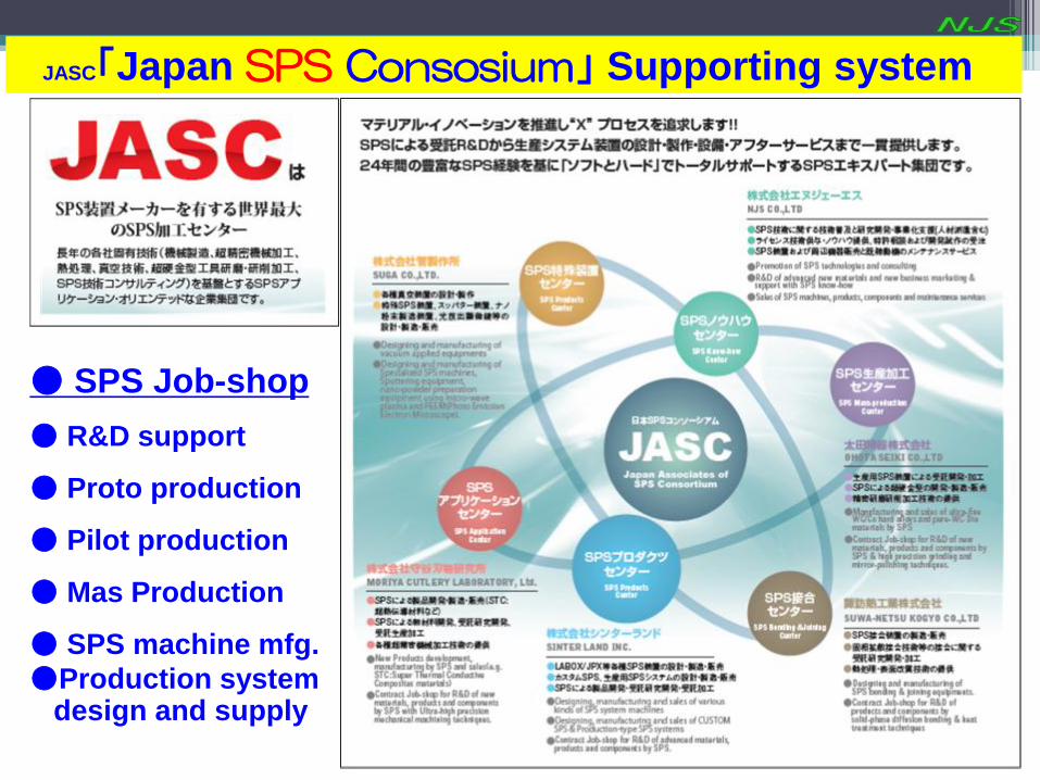
JASC「Japan SPS Consosium」 Supporting system
● SPS Job-shop
● R&D support
● Proto production
● Pilot production
● Mas Production
● SPS machine mfg.
●Production system design and supply

Advantage & Disadvantage
• Rapid sintering
• & high heating-up
• High quality sintered compact
• (finer microstructure)
• Mass-production
• & Cost ?
● Easy to receive
SPS machine damages
● Difficult to determine optimum SPS sintering Conditions on Large size and/or complex shape
● Die and punch Life time Cycle time, maintenance and Raw powder cost (possibly 24 hours operation)

The SPS still have a variety of practical industrial applications issues to be solved before the full potential of the SPS manufacturing processes are realized.
The example results suggested that the SPSed large size ceramics usually contained higher residual stresses than small size inside of the sintered body, and especially their SPS temperature distribution behavior difference in the powder material during heating-up, even applying the same SPS sintering conditions. Determination of the optimized SPS process conditions on the different ceramics materials is now in progress for practical industrialization.
These issues include enlarging process, homogenization technique, reduction of residual stresses, shape & size effects and system automation, increasing the pulse current density control and capacity, and versatility of functions in the hardware, and the creation of a SPS sintering technology data base and improvements to reliability and reproducibility in terms of software.
It is also important to develop suitable powder materials and establish 3-D forming fabrication techniques according to the required SPS applications so that they match the characteristics of the SPS Production process and systems.
OUTLOOK & SUMMARY

SPS brings the world together - Rainbow in Maui, Hawaii -
Pac-Rim 6 / 2005 Sep. Thank you !!


![12-01-02 CarboMetal Poster€¦ · powder [SPS: Spark Plasma Sintering, HIP: Hot Isostatic Pressing] Synthesis of Al- and Cu-coated CNTs (Electroless Plating Process / Chemical and](https://static.fdocuments.net/doc/165x107/6085964762a9da2c892a410e/12-01-02-carbometal-powder-sps-spark-plasma-sintering-hip-hot-isostatic-pressing.jpg)