Real Time Clock USB Evaluation Board User Guide · Real Time Clock USB Real Time Clock USB...
14
USER’S MANUAL AN1745 Rev 2.00 October 9, 2013 Real Time Clock USB Real Time Clock USB Evaluation System AN1745 Rev 2.00 Page 1 of 14 October 9, 2013 Introduction This evaluation system is a hardware and software platform for testing Intersil Real Time Clock (RTC) devices, and the system requires only a PC for the controller and power functions. Intersil offers a large portfolio of RTC devices, with features including a crystal oscillator, clock and date counters, auto switch-over to battery backup, voltage monitoring with low voltage reset, a watchdog timer, and alarms. The ISL1209/19/21/32 devices include an event-detection feature, and all but the ISL1209 include a time stamp function for recording the time of the event. The ISL12022 features an on-chip temperature sensor and temperature compensation, while the ISL12020M/22M/22MA devices are RTC modules with internal crystals. These module versions are factory calibrated to account for crystal variability, and the on-chip temperature sensor enables automatic crystal temperature compensation, for the best RTC accuracy over temperature. The evaluation system enables users to test all of these functions, and to evaluate device performance criteria, such as long-term clock accuracy. Hardware options, such as battery and crystal types, can also be tested. The software sets up easily, and enables evaluation of all major RTC functions. The hardware’s two-piece construction - utilizing a motherboard and a daughterboard - allows the evaluation of multiple RTC products simply by switching out small daughterboards. Operation and Overview of the RTC Evaluation Board Connections The evaluation board consists of a motherboard and daughterboard which connect together via J1 and J2. The hardware uses a USB connection to communicate with the PC loaded software, and USB drivers must be installed on the PC. The provided USB cable, with type A and B connectors, is required to hook up the board to a PC. The cable should be connected to the PC first and then to the evaluation board. Once connected, you will hear the USB “enumeration” tone, and the motherboard “POWER” LED illuminates, indicating that the USB connection is providing the +5V power. Powering Down The motherboard contains backup power sources, either a supercap or an optional battery, so the RTC might operate off a backup source when V DD powers down. If the user wishes to totally power down the RTC device (e.g., a hard reset), either disconnect the daughterboard from the motherboard or connect motherboard jumper J4 to the “GND” position to eliminate the backup sources. There is a 0.1μF V DD decoupling capacitor on the daughterboard, which must discharge fully before the RTC device stops operating. This discharge time can be up to one second when using a V DD of 5V. Note that when powered down, the RTC board cannot be monitored by the RTC evaluation software. Installing the RTC Software and USB Drivers • Note: If you have previously loaded the Intersil RTC evaluation software on the PC, you need to uninstall the previously loaded version of the Intersil RTC Evaluation software on the PC, Navigate to the uninstall program “All Programs > Intersil > RTC_EVAL > RTC_uninstall” and run it. If the uninstall program did not delete the old desktop shortcut (right click on icon, then “delete”). Last you need to uninstall the USB drivers before running the following install. Go to Device Manager, (Control Panel, System, Hardware) with the Eval board plugged in. Locate the “USBXpress Device” under the “Universal Serial Bus controllers” branch and then right click and select the “Uninstall”. • Download the appropriate Installation program from the Web. The same installation file is used for all Intersil RTC Products, but changes for the Windows Version your computer is running. The basic link to these installers is: http://www.intersil.com/content/dam/Intersil/documents/ rtc_/ (add Web File name from below) or go to the products main page and select the “Documents” tab. • For Windows 2000 the Web File name is “RTC_EVAL_Installer_w2k_V405.exe” • For Windows XP & WIN7 the Web File name is “RTC_EVAL_Installer_V405.exe” • For Windows 8, the Web File name is “RTC_EVAL_Installer_Win8_V405.exe” • WIN8 Note: Before running the WIN8 installer there is a pre- installation document on the Web that must be followed. File name is RTC_WIN8_Preinstallation_Procedure_081613.PDF. Download this file, open it and follow the procedure. • Do not plug in the RTC USB evaluation board yet. • Double click on “RTC_EVAL_Installer...”. • Click “Next”. • If you agree with the license conditions, click “I accept” in the license window, then click “Next” to install. • Select a “Destination Location”, and click “Next”. • Select a “Start Menu Folder”, and click “Next”. • Click on “Create a Desktop Icon” and click “Next”. Intersil RTC Devices Supported WITH USER EEPROM NO USER EEPROM ISL12024 ISL1208 ISL12020M ISL12025 ISL12008 ISL12022M ISL12026/26A ISL1209 ISL12022MA ISL12027/27A ISL1218 ISL12032 ISL12028/28A ISL1219 ISL12057 ISL12029/29A ISL1220 ISL12058 ISL1221 ISL12059 ISL12022 ISL12082
Transcript of Real Time Clock USB Evaluation Board User Guide · Real Time Clock USB Real Time Clock USB...
USER’S MANUAL
AN1745Rev 2.00
October 9, 2013
Real Time Clock USBReal Time Clock USB Evaluation System
IntroductionThis evaluation system is a hardware and software platform for testing Intersil Real Time Clock (RTC) devices, and the system requires only a PC for the controller and power functions. Intersil offers a large portfolio of RTC devices, with features including a crystal oscillator, clock and date counters, auto switch-over to battery backup, voltage monitoring with low voltage reset, a watchdog timer, and alarms. The ISL1209/19/21/32 devices include an event-detection feature, and all but the ISL1209 include a time stamp function for recording the time of the event. The ISL12022 features an on-chip temperature sensor and temperature compensation, while the ISL12020M/22M/22MA devices are RTC modules with internal crystals. These module versions are factory calibrated to account for crystal variability, and the on-chip temperature sensor enables automatic crystal temperature compensation, for the best RTC accuracy over temperature.
The evaluation system enables users to test all of these functions, and to evaluate device performance criteria, such as long-term clock accuracy. Hardware options, such as battery and crystal types, can also be tested. The software sets up easily, and enables evaluation of all major RTC functions. The hardware’s two-piece construction - utilizing a motherboard and a daughterboard - allows the evaluation of multiple RTC products simply by switching out small daughterboards.
Operation and Overview of the RTC Evaluation BoardConnections The evaluation board consists of a motherboard and daughterboard which connect together via J1 and J2. The hardware uses a USB connection to communicate with the PC loaded software, and USB drivers must be installed on the PC. The provided USB cable, with type A and B connectors, is required to hook up the board to a PC. The cable should be connected to the PC first and then to the evaluation board. Once connected, you will hear the USB “enumeration” tone, and the motherboard “POWER” LED illuminates, indicating that the USB connection is providing the +5V power.
Powering DownThe motherboard contains backup power sources, either a supercap or an optional battery, so the RTC might operate off a backup source when VDD powers down. If the user wishes to totally power down the RTC device (e.g., a hard reset), either disconnect the daughterboard from the motherboard or connect motherboard jumper J4 to the “GND” position to eliminate the backup sources. There is a 0.1µF VDD decoupling capacitor on the daughterboard, which must discharge fully before the RTC device stops operating. This discharge time can be up to one second when using a VDD of 5V. Note that when powered down, the RTC board cannot be monitored by the RTC evaluation software.
Installing the RTC Software and USB Drivers• Note: If you have previously loaded the Intersil RTC
evaluation software on the PC, you need to uninstall the previously loaded version of the Intersil RTC Evaluation software on the PC, Navigate to the uninstall program “All Programs > Intersil > RTC_EVAL > RTC_uninstall” and run it. If the uninstall program did not delete the old desktop shortcut (right click on icon, then “delete”). Last you need to uninstall the USB drivers before running the following install. Go to Device Manager, (Control Panel, System, Hardware) with the Eval board plugged in. Locate the “USBXpress Device” under the “Universal Serial Bus controllers” branch and then right click and select the “Uninstall”.
• Download the appropriate Installation program from the Web. The same installation file is used for all Intersil RTC Products, but changes for the Windows Version your computer is running. The basic link to these installers is: http://www.intersil.com/content/dam/Intersil/documents/rtc_/ (add Web File name from below) or go to the products main page and select the “Documents” tab.
• For Windows 2000 the Web File name is “RTC_EVAL_Installer_w2k_V405.exe”
• For Windows XP & WIN7 the Web File name is “RTC_EVAL_Installer_V405.exe”
• For Windows 8, the Web File name is “RTC_EVAL_Installer_Win8_V405.exe”
• WIN8 Note: Before running the WIN8 installer there is a pre-installation document on the Web that must be followed. File name is RTC_WIN8_Preinstallation_Procedure_081613.PDF. Download this file, open it and follow the procedure.
• Do not plug in the RTC USB evaluation board yet.
• Double click on “RTC_EVAL_Installer...”.
• Click “Next”.
• If you agree with the license conditions, click “I accept” in the license window, then click “Next” to install.
• Select a “Destination Location”, and click “Next”.
• Select a “Start Menu Folder”, and click “Next”.
• Click on “Create a Desktop Icon” and click “Next”.
Intersil RTC Devices SupportedWITH USER EEPROM NO USER EEPROM
ISL12024 ISL1208 ISL12020M
ISL12025 ISL12008 ISL12022M
ISL12026/26A ISL1209 ISL12022MA
ISL12027/27A ISL1218 ISL12032
ISL12028/28A ISL1219 ISL12057
ISL12029/29A ISL1220 ISL12058
ISL1221 ISL12059
ISL12022 ISL12082
AN1745 Rev 2.00 Page 1 of 14October 9, 2013
Real Time Clock USB
• Click “Install” (you might get an error here if installing on an OS older than XP, but disregard).
• In “Motherboard Driver Installer” window, click “Install”.
• In pop-up window, click on “Install the Driver Software Anyway” (Win 7 and Win 8 only).
• Click “OK”, and then click “Finish”.
The following instructions apply only to non WIN 7 and WIN8 systems:
• After the software install, plug in the USB cable and motherboard, and the hardware installation wizard should appear.
• If asked for the location of drivers, use C:/Program Files (x86)/Intersil/RTC_EVAL/USB_Driver directory as the source. Note (x86) only for WIN7 & WIN8 Systems.
• Click “Next” to install the drivers and then “Finish” to complete the installation.
The installation program places the RTC evaluation software (RTC13.exe) in: C:\Program Files (x86)\Intersil\RTC Eval on a WIN7 and WIN8 PC, or in C:\Program Files\Intersil\RTC Eval on an XP or older PC.
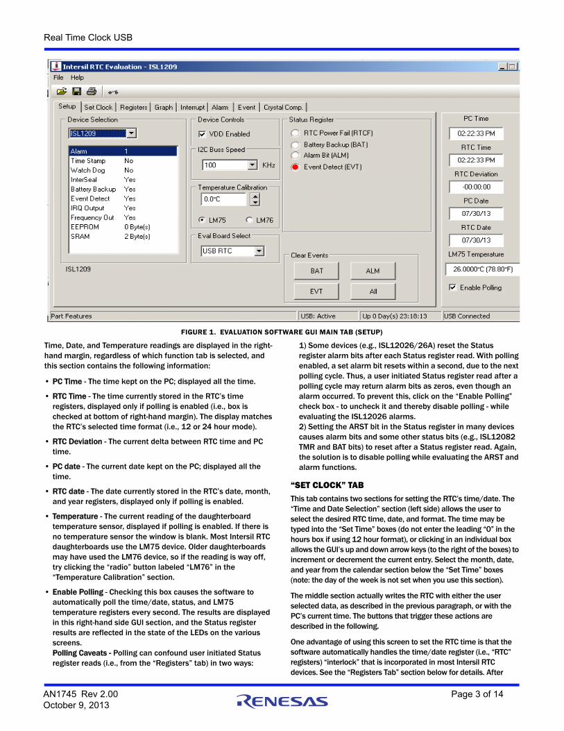
Using the SoftwareTo start the evaluation software, double click on the Desktop “RTC Evaluation” icon, or double click on C:\Program Files\Intersil\RTC Eval\RTC13.exe and the GUI (Graphical User Interface) should appear as shown in Figure 1. This first screen is the “Setup” page, as indicated on the function tab near the top of the GUI. The screen’s bottom margin contains USB connection status messages, with the center message indicating if the USB device is disconnected or active.
There are multiple tabs (e.g., “Set Clock”) at the top of the GUI. These tabs take the user to screens for setting up the RTC and for controlling its functions, and each of the tabs is discussed in the following sections.
There are icons in the top tool bar to print the register contents and the “Graph” screen deviation plot, and to control VDD to the daughterboard. The printer icon prints the current register values, and the “RTC Deviation” plot from the “Graph” screen, to the PC’s default printer. To print the actual register values, the user must first use the “Register” tab to read the current contents of all registers. Simply select a register group from the drop-down box, and then click the “Page Operation” “Read” button. Repeat the process until all register groups have been read, and it is best to read the “RTC” group last, so the time/date registers are as up to date as possible. The switch icon toggles the daughtercard VDD from disabled (open switch icon) to enabled (closed switch icon), and vice versa. The icons remain visible from all screens, as do the polled RTC values displayed in the right-hand margin.
There are three common causes if the following error box appears during a read or write cycle with the RTC:
1. The PC has powered down, gone into screen lock, and powered back up. Unplugging and replugging the USB cable fixes this problem.
2. The “VDD Enabled” check box on the “Setup” screen isn’t checked, or
3. The daughtercard’s “DEV VCC” (or “JVDD”) jumper is missing.Correcting these three problems should eliminate the error.
“SETUP” TABThere are three sections to the Setup screen, plus a time/date/temperature display section. The left section indicates the selected RTC device, and that RTC’s features are listed in the large text box. RTC selection is via the drop-down box, and the device selection determines which other tabs the GUI displays.
The middle left section has five functions. The “VDD Enabled” check box controls the motherboard’s RTC VDD switch. Clicking this check box enables or disables VDD to the daughterboard, and to the I2C pull-up resistors. Note that when this box is unchecked, no communication with the RTC daughterboard is possible. The switch icon in the GUI’s top tool bar performs the same function as the “VDD Enabled” check box. With VDD on, clicking the switch icon shuts off the daughterboard’s VDD, and the icon displays an open switch. Clicking the icon again, reapplies VDD and the icon displays a closed switch. The I2C bus speed - either 100kHz or 400kHz - is selected from the middle drop-down box. The temperature sensor type (daughterboards have either an LM75 or an LM76) is selected via the two “radio” buttons, with the default value being the more common “LM75”. A nonsensical reading in the “LM75 Temperature” box in the right-hand margin may indicate that the daughterboard contains an LM76. The sensor’s temperature value can be calibrated by adding an offset to the sensor reading via the “Temperature Calibration” box. Set the “Eval Board Select” drop-down box to “USB RTC”.
The middle right section is the Status register display and event reset section (this latter feature is only for the ISL1208 through ISL1221). The relevant status bits for the selected RTC are displayed as lights in the upper section and those bits can be cleared using the buttons in the lower section.
AN1745 Rev 2.00 Page 2 of 14October 9, 2013
Real Time Clock USB
Time, Date, and Temperature readings are displayed in the right-hand margin, regardless of which function tab is selected, and this section contains the following information:
• PC Time - The time kept on the PC; displayed all the time.
• RTC Time - The time currently stored in the RTC’s time registers, displayed only if polling is enabled (i.e., box is checked at bottom of right-hand margin). The display matches the RTC’s selected time format (i.e., 12 or 24 hour mode).
• RTC Deviation - The current delta between RTC time and PC time.
• PC date - The current date kept on the PC; displayed all the time.
• RTC date - The date currently stored in the RTC’s date, month, and year registers, displayed only if polling is enabled.
• Temperature - The current reading of the daughterboard temperature sensor, displayed if polling is enabled. If there is no temperature sensor the window is blank. Most Intersil RTC daughterboards use the LM75 device. Older daughterboards may have used the LM76 device, so if the reading is way off, try clicking the “radio” button labeled “LM76” in the “Temperature Calibration” section.
• Enable Polling - Checking this box causes the software to automatically poll the time/date, status, and LM75 temperature registers every second. The results are displayed in this right-hand side GUI section, and the Status register results are reflected in the state of the LEDs on the various screens.Polling Caveats - Polling can confound user initiated Status register reads (i.e., from the “Registers” tab) in two ways:
1) Some devices (e.g., ISL12026/26A) reset the Status register alarm bits after each Status register read. With polling enabled, a set alarm bit resets within a second, due to the next polling cycle. Thus, a user initiated Status register read after a polling cycle may return alarm bits as zeros, even though an alarm occurred. To prevent this, click on the “Enable Polling” check box - to uncheck it and thereby disable polling - while evaluating the ISL12026 alarms.2) Setting the ARST bit in the Status register in many devices causes alarm bits and some other status bits (e.g., ISL12082 TMR and BAT bits) to reset after a Status register read. Again, the solution is to disable polling while evaluating the ARST and alarm functions.
“SET CLOCK” TABThis tab contains two sections for setting the RTC’s time/date. The “Time and Date Selection” section (left side) allows the user to select the desired RTC time, date, and format. The time may be typed into the “Set Time” boxes (do not enter the leading “0” in the hours box if using 12 hour format), or clicking in an individual box allows the GUI’s up and down arrow keys (to the right of the boxes) to increment or decrement the current entry. Select the month, date, and year from the calendar section below the “Set Time” boxes (note: the day of the week is not set when you use this section).
The middle section actually writes the RTC with either the user selected data, as described in the previous paragraph, or with the PC’s current time. The buttons that trigger these actions are described in the following.
One advantage of using this screen to set the RTC time is that the software automatically handles the time/date register (i.e., “RTC” registers) “interlock” that is incorporated in most Intersil RTC devices. See the “Registers Tab” section below for details. After
FIGURE 1. EVALUATION SOFTWARE GUI MAIN TAB (SETUP)
AN1745 Rev 2.00 Page 3 of 14October 9, 2013
Real Time Clock USB
using the “Set Clock” function, and if polling is enabled, the new RTC time/date are displayed in the right-hand margin.
The “buttons” on this screen perform the following functions:
• Write RTC Eval Board from PC Clock - Clicking this button reads the PC’s time and date values, and writes them to the RTC’s registers. This is a one button method to completely initialize the RTC’s time/date registers.
• Set RTC Date and Time - Use this button to write the data from the “Time and Date Selection” section into the RTC’s registers.
• Get RTC Date and Time - Clicking this button populates the “Time and Date Selection” windows with the RTC’s current time/date. These values can then be edited, and rewritten to the RTC.
• Set PC Time and Date from RTC Eval Board - This button writes the RTC’s current time/date to the PC’s clock. Using this button is not encouraged, as the current PC time and date are lost.
“REGISTERS” TAB This tab enables reading from, and writing to, any of the registers in the selected RTC device. Pick a register - or register group - from the drop-down box below the tabs, and the screen displays those registers, but not their contents (cell’s gray shading indicates an indeterminate value). Click on the “Page Operation” “Read” button (below registers on the GUI’s left side), and the registers’ contents are now displayed (white boxes represent zeros, blue boxes represent ones). Initiating a page read is always the recommended first step after selecting a register group. The read populates the screen with current register values, which helps prevent writing out of date data (e.g., a previous time) into registers - or bits - that aren’t being actively changed. The “Read” button at the right of each register row (under the “Byte Operation” heading) reads that individual register’s contents.
There are two ways to set the data when writing to a register:1) Enter the hex value for the desired data into the “Hex” column to the right of the register’s name. Note that the register’s displayed data changes to match the hex code.2) Enter the desired value bit-by-bit in the register cells. To change an individual bit, click on it to toggle its value. Note that clicking a bit in an unread register - i.e., the cell colors are gray - does not cause a register read, so the data subsequently displayed are not the register’s true contents. Clicking the register’s write button, or the “Page Write” button causes this bad data to be written to the register(s), so it is strongly recommended that a register or page read be executed immediately before changing any register bits.After editing a register’s contents, click the “Byte Operation” column “Write” button to write a single register, or click the “Page Operation” “Write” button after updating multiple registers.
Operations initiated on screens under other function tabs may change the RTC’s registers, and those results are only displayed on the “Registers” screen after a subsequent read operation. Also, changes made on the Registers screen are reflected on the corresponding function’s screen only after clicking that tab/function’s “Read” button. When reading the Status register, note the “Polling Caveats” listed at the bottom of the previous “Setup Tab” section.
Time/Date Register Interlocks
Nearly all Intersil RTC devices have an interlock feature that requires special bits to be set before the time/date (“RTC”) registers can be written. The majority of interlocked devices (e.g., the ISL1208) have a “WRTC” bit in the Status or INT register, and this bit must be written to a “1” before the RTC registers can be written. The evaluation software does NOT return an error if the user attempts to write the RTC registers when WRTC=0, so you must remember to check the state of the WRTC bit if the time doesn’t update after the write cycle.
The ISL12024/25/26/27/28/29 use a two bit, Status register WEL/RWEL interlock, where a special combination of writes is required to unlock any register (RTC, Status, Control, Alarm, etc.) for writing. To simplify register writes, this family’s Register screens include an “Unlock” button, and an “Enable Auto Unlock” check box. Checking the “Enable Auto Unlock” box (software’s default setting) causes the software to automatically set the WEL and RWEL bits during each write command, so the user doesn’t have to worry about unlocking the registers. Clicking the “Unlock” button causes the evaluation software to properly set the WEL and RWEL bits, so a subsequent write command executes as desired. Note that the RWEL bit resets after every register write cycle (WEL stays set), so click the “Unlock” button before every register write command (byte or page), or use the “Enable Auto Unlock” function. A few devices (ISL12008, ISL12057, ISL12058, ISL12059) have no interlock, so the time registers can be written without being unlocked.
“SRAM” OR “EEPROM” TAB This tab allows the user access to the on-chip general purpose memory, if the RTC has it. The memory is battery backed SRAM on some devices (ISL12020M/22/22AM/22M/32), and EEPROM on others (ISL12024-29).
To read or write an individual memory byte, click on the cell in the displayed matrix, and the address appears in the “Byte R/W” section. Click the “Read” button to see the cell’s contents, or enter the hex data in the box next to the “Write-Adr” box, and click the “Write” button to change the byte. Click the “Read” or “Read All” button to display what was just written.
To show all the memory bytes’ contents in the display matrix, click the “Read All” button, noting that the memory may contain random data if it has not been written previously. If desired, all of the memory bytes may be written simultaneously using the “Write All” button. First, select one of the “Fill Options” by clicking one of the four “radio” buttons under that heading. “Data=Adr” writes the cell’s address into its memory location, while “Checkerboard” writes the two user defined data bytes to adjacent memory bytes. “Explicit1” and “Explicit2” allow the user to define two different data bytes that may be written to the entire memory array. After choosing the desired fill option, click the “Write All” button to write the memory array. Remember to click “Read All” to display what was just written.
“GRAPH” TABThe RTC evaluation software records continuous measurements of the RTC time to PC reference clock deviation, and of the board temperature. The Graph tab then allows the user to display the results vs. elapsed time, for times extending from a few minutes to thirty days.
AN1745 Rev 2.00 Page 4 of 14October 9, 2013
Real Time Clock USB
To create a graph, select the “Deviation Range” from the drop-down box in the lower left corner, and select the “Temp Range” from the box on the right, to set the vertical axes’ ranges. Select the “Time Base” (measurement time duration) from the box in the middle, to define the horizontal axis range. Note that the ranges may be changed at any time, and the data scales accordingly. Data exceeding the “Time Base” is still collected, and is displayed if the time base is increased.
Set the RTC time from the PC time as described previously. This ensures that the RTC time matches the PC time when recording starts. Ensure that the “Enable Polling” box is checked, and that there is a near zero value in the “RTC Deviation” box in the right-hand margin.
To begin recording, click the “Restart” button at the GUI’s bottom right. The graph automatically records and plots the data as long as the polling function is enabled. Graphing stops when polling is disabled, and starts again when polling is re-enabled. Once re-enabled, the new data point is plotted at the proper elapsed time point. The graphing function connects the last data point to this new data point, so the data between these two points is meaningless. To start a new graph, click the “Restart” button.
Data is recorded periodically until polling is stopped. Multiple samples are measured and averaged before being plotted on the chart recorder.
The raw data can be saved to a file for analysis or for storage. Choose a file directory and name using the “Open Folder” icon in the tool bar, then click the “Save File” icon to save the chart data. The top of the file contains a list of registers and values; see the third paragraph of the “Using the Software” section for how to ensure that the register list provides meaningful data. Subsequent clicks on the save icon overwrite the previous file with the latest data, without prompting for permission. The file is overwritten even if it is open when save is clicked, but you will have to close, and then reopen the file to see the updates.
The data collection start time remains in the “Start Time” box for reference. Note that for long duration recordings of deviation, it is advisable to use a PC program that automatically updates the PC time, such as that available from NIST http://www.boulder.nist.gov/timefreq/service/its.htm.
“INTERRUPT”, “FOUT”, AND “FOUT & IRQ” TABSThese tabs allow the user to select the frequency of the FOUT pin, to select whether or not the FOUT pin is active in battery backup mode, and on some devices (e.g., the ISL1208) to enable the alarm IRQ output. Click the “Read” button to determine the current state of the settings, and remember to click on the “Write” button after making any changes to those settings (even after clicking on a check box).
The drop-down box at the top left allows the selection of the FOUT frequency. On many devices the first (0Hz) or last entry in the drop-down box switches the multifunction IRQ/FOUT pin to the alarm interrupt (IRQ) mode. The ISL12058 also requires the checking of the “Enable Alarm1” box to activate the IRQ function, and the ISL12057’s IRQ pin control is on the “Alarm & IRQ” screen.
Many of these RTC screens include a “Disable Frequency Out in Battery Mode” check box, and checking this box disables the FOUT pin whenever the RTC enters battery back-up mode.
“ALARM” TABThe alarm tab provides an easy way for users to define software alarms - indicated by the Status register alarm bits - and hardware alarm interrupts (IRQ outputs), when available. Click the “Read” button to determine the current state of the settings, and remember to click on the “Write” button after making any changes to those settings (even after clicking on a check box). For the best results, set up the alarm time/date triggers before enabling an alarm.
The screen provides drop-down boxes to select the alarm time/date trigger conditions. Selecting “Ignore” in the drop-down box prevents that time/date component from being used to determine an alarm match. For example, a “10” in the “Seconds” box with “Ignore” in all the other boxes means that an alarm is generated whenever the time has “10” in the “seconds” position. Note that the “Hours” drop-down box contains entries for both military and 12 hour time formats, and the selected “Hours” value must correspond to the chosen time format, or the alarm will not trigger.
Check boxes at the top of most alarm set-up boxes control whether or not an alarm is enabled (i.e., generates software and/or hardware alarms), and select either normal or repetitive pulsed interrupt mode (IM). Note that the actual hardware alarm pin (IRQ output) usually is enabled via the “Interrupt” screen, as previously described.
The “Alarm Status” “LED” below the alarm set-up box reflects the Status register alarm bit state. The “Manual Clear Event” button(s) at the GUI bottom resets the appropriate Status register alarm bit, and thus the “LED”.
“EVENT” TAB (ISL1209, 1219, 1221, 12032 ONLY)This tab appears if the chosen RTC includes an Event Detection - also know as “Tamper Detection” - feature. This screen allows the user to control the event detection parameters, and the event time stamp functions, when available. Click the “Read” button to determine the current state of the settings, and remember to click on the “Write” button after making any changes to those settings (even after clicking on a check box).
The left side of the screen contains the controls for the EV register. The top check box (EVEN) enables the event detection function, and once checked and written it also activates the sample rate (ESMPL) and hysteresis (EHYS) drop-down boxes. The lower three check boxes select whether or not the RTC stops incrementing the time once an event occurs (RTCHLT), whether or not the event input (EVIN) pull-up current source is enabled (EVIENB), and whether or not the event detection function is enabled in battery backup mode (EVBATB). For these last two functions, note that checking the box disables the function.
The right side of the screen includes the “Event Detect” “LED”, and the event time stamp display window (not available on the ISL1209). The LED indicates the Status register EVT bit state, but is not available on the ISL12032. The ISL1219 and ISL1221 time stamp register locks after the first event. Once the Status register EVT bit is reset, the time stamp register unlocks, and records the next event time stamp. The ISL12032 screen displays the first event time stamp - which locks until cleared - the last three event time stamps, and an event counter. The screen also includes
AN1745 Rev 2.00 Page 5 of 14October 9, 2013
Real Time Clock USB
buttons to read time stamps, and to clear the four time stamp registers and the time stamp counter.
After setting up the parameters and enabling events, pushing the “Event” button (S1 or EVIN) on the evaluation board lights the “Event Detect” LED, and loads the current time into the time stamp register (unless the register is locked).
“CRYSTAL COMP” TABThis tab appears if the chosen RTC includes a crystal compensation feature, which allows the user to calibrate out crystal tolerances, or to compensate a crystal for temperature effects. For most RTC devices, this screen includes control boxes for the fine adjust analog trim (ATR) setting, and for the course adjust digital trim (DTR) setting. Some devices also include a Battery Mode ATR (BMATR) control box, which allows the user to select a different level of compensation when the RTC is in battery backup mode.
“SYSMGMT” TABThis tab appears if the chosen RTC has an unusual system feature. For example, this tab allows the software to control the ISL12029’s programmable I2C bus watchdog timeout and programmable low VDD Reset threshold functions. For the ISL12032, this tab provides control over the RTC’s AC power functions.
“DST” TABSelect an RTC that includes a daylight savings time (DST) function, and the evaluation software displays this tab. From this screen the user can set the trigger time/date for the RTC to enter DST (i.e., DST forward) and the trigger time/date for the RTC to return to standard time (i.e., DST reverse). The “DST Forward Adjust” “LED” reflects the state of the Status register DSTADJ bit, so it lights when the RTC switches to DST, and it extinguishes when the RTC returns to standard time. The LED does not light when the RTC is initialized to a time between the “DST Forward” and “DST Reverse” times.
Note: To get the daylight savings time adjustment (forward or backward) to occur the next time the RTC time hits the trigger setting, the set trigger time must be at least one hour after the current RTC time when the DST function is enabled (by checking this screen’s “DST Enable” check box, or by setting the DstMoFd register’s DSTE bit).
“TEMPCOMP” TABThe ISL12022, ISL12020M, ISL12022M, and ISL12022MA feature an on-chip temperature sensor, and accompanying crystal temperature compensation circuitry, and this tab controls those functions. Click the “Read” buttons to determine the current state of the settings, and remember to click on the appropriate “Write” button after making any changes to those settings (even after clicking on a check box). The “Write Mode” and “Read Mode” buttons operate on the entries in the “Temperature Sense Control” box, while the “Write Comp Regs” and “Read Comp Regs” buttons operate on the entries in the “Temp Coefficient & Gain”, “Final Trim”, and “Initial Trim” boxes.
The ISL12022 operation is different than the ISL12020M and ISL12022M, in that the ISL12022 “Temp Coefficient & Gain” registers are writable, while they are “Read Only” on the other
two RTCs. Before writing these ISL12022 registers, make sure that temperature sensing is disabled (i.e., uncheck the “Temp Sense Enable” [TSE] box, and click “Write Mode”).
Temperature sensing can be enabled for only normal VDD operation (check only the TSE box), or for VDD and battery backup operation. For all three RTCs, to enable temperature sensing in both modes: click TSE first, then “Write Mode”, then click “Battery Mode Temp Sense Enable” (BTSE) followed by “Write Mode”. After writing BTSE note that the “TSE period in Battery Mode” box changes from “OFF” to a time interval, which is the interval at which temperature sensing occurs in battery backup mode. Clicking the “Battery Mode Temp Sense Period” box followed by “Write Mode” toggles the “TSE Period” box between “10 Minute” (box unchecked), and “1 Minute” (box checked).
After enabling temperature sensing, read the RTC’s temperature by clicking the “Read Mode/Temp” button toward the bottom left of the screen. Note that successive reads return the same temperature value, unless a new sense cycle occurred.
The ISL12022X default, non-backup mode, temperature sense interval is once per minute. Clicking the “Write Mode” button, with the “TSE” box checked, forces an immediate sense cycle. To force more frequent, automatic updates, go to the “Interrupt” tab, and select an update interval from the “TSE Refresh” drop-down box, and click “Write”. For example, selecting “5” from the drop-down box causes the evaluation software to trigger a temperature sense cycle every 5 seconds. The user must still click “Read Mode/Temp” under the “TempComp” tab to display the updated temperature.
“PWRMGMT” TABThis tab appears if the chosen RTC includes low VDD and low VBAT monitoring functions. From this screen the user can set the desired trigger thresholds for the LVDD status bit, and for the VBAT’s 85% (LBAT85) and 75% (LBAT75) threshold status bits. This screen also displays time stamps that indicate when the RTC first entered battery backup (VDD-to-VBAT), and when the RTC last returned to VDD operation from battery backup (VBAT-to-VDD). Time stamps may be cleared via the CLRTS button. The ISL12032 includes an on-chip battery trickle charger, and the control for this function is on the PWRMGMT screen.
Detailed Hardware DescriptionRTC USB Evaluation Platform - General DescriptionThe RTC evaluation hardware consists of a universal motherboard, and a daughterboard specific to the RTC being evaluated.
AN1745 Rev 2.00 Page 6 of 14October 9, 2013
Real Time Clock USB
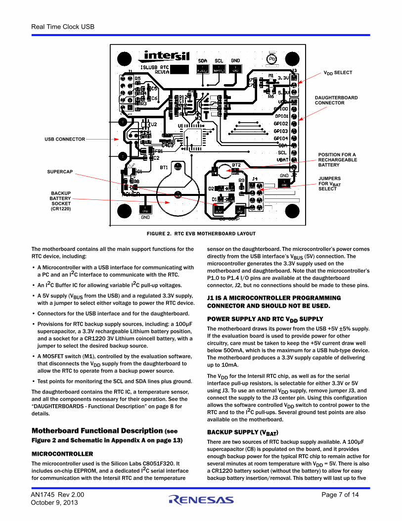
The motherboard contains all the main support functions for the RTC device, including:
• A Microcontroller with a USB interface for communicating with a PC and an I2C interface to communicate with the RTC.
• An I2C Buffer IC for allowing variable I2C pull-up voltages.
• A 5V supply (VBUS from the USB) and a regulated 3.3V supply, with a jumper to select either voltage to power the RTC device.
• Connectors for the USB interface and for the daughterboard.
• Provisions for RTC backup supply sources, including: a 100µF supercapacitor, a 3.3V rechargeable Lithium battery position, and a socket for a CR1220 3V Lithium coincell battery, with a jumper to select the desired backup source.
• A MOSFET switch (M1), controlled by the evaluation software, that disconnects the VDD supply from the daughterboard to allow the RTC to operate from a backup power source.
• Test points for monitoring the SCL and SDA lines plus ground.
The daughterboard contains the RTC IC, a temperature sensor, and all the components necessary for their operation. See the “DAUGHTERBOARDS - Functional Description” on page 8 for details.
Motherboard Functional Description (see Figure 2 and Schematic in Appendix A on page 13)
MICROCONTROLLERThe microcontroller used is the Silicon Labs C8051F320. It includes on-chip EEPROM, and a dedicated I2C serial interface for communication with the Intersil RTC and the temperature
sensor on the daughterboard. The microcontroller’s power comes directly from the USB interface’s VBUS (5V) connection. The microcontroller generates the 3.3V supply used on the motherboard and daughterboard. Note that the microcontroller’s P1.0 to P1.4 I/O pins are available at the daughterboard connector, J2, but no connections should be made to these pins.
J1 IS A MICROCONTROLLER PROGRAMMING CONNECTOR AND SHOULD NOT BE USED.
POWER SUPPLY AND RTC VDD SUPPLYThe motherboard draws its power from the USB +5V ±5% supply. If the evaluation board is used to provide power for other circuitry, care must be taken to keep the +5V current draw well below 500mA, which is the maximum for a USB hub-type device. The motherboard produces a 3.3V supply capable of delivering up to 10mA.
The VDD for the Intersil RTC chip, as well as for the serial interface pull-up resistors, is selectable for either 3.3V or 5V using J3. To use an external VDD supply, remove jumper J3, and connect the supply to the J3 center pin. Using this configuration allows the software controlled VDD switch to control power to the RTC and to the I2C pull-ups. Several ground test points are also available on the motherboard.
BACKUP SUPPLY (VBAT)There are two sources of RTC backup supply available. A 100µF supercapacitor (C8) is populated on the board, and it provides enough backup power for the typical RTC chip to remain active for several minutes at room temperature with VDD = 5V. There is also a CR1220 battery socket (without the battery) to allow for easy backup battery insertion/removal. This battery will last up to five
FIGURE 2. RTC EVB MOTHERBOARD LAYOUT
SUPERCAP
BACKUPBATTERYSOCKET
VDD SELECT
DAUGHTERBOARDCONNECTOR
JUMPERSFOR VBATSELECT
USB CONNECTOR
POSITION FOR A RECHARGEABLEBATTERY
(CR1220)
AN1745 Rev 2.00 Page 7 of 14October 9, 2013
Real Time Clock USB
years in normal backup operation. The backup source is selectable via jumper J4 as shown in Figure 2. The right-hand column of J4 connects to the RTC VBAT pin (J2 pin 9), and the other column connects to the power sources. There are four positions possible on J4: Supercap (SCAP), rechargeable battery (BT2, user must install a suitable battery holder, but the charging diode [D2] and resistor [R9] are populated), CR1220 Battery (BT1), and ground (GND). If no backup is required, then the “GND” position should be used. To use an alternate VBAT source, remove the jumper and connect the source to any of the right-hand column pins.
DAUGHTERBOARD CONNECTOR (J2)J2 is a 10 pin, female connector. The RTC daughterboard plugs into this connector, which provides power - VDD, VBAT, and GND - and interface signals (SDA, SCL) to the RTC device, and to other components on the daughterboard. The signals are labeled on the motherboard silkscreen.
USB CONNECTOR (CON1)This connector is a standard USB type B connector, which connects to the USB port of a PC using a USB type A-B cable (included with the evaluation system). The cable must be plugged into a PC for VDD power to be applied to the RTC, but depending on the position of J4, the RTC may operate off backup power with the cable disconnected.
POWER/USB ACTIVITY INDICATORThere is one surface mounted LED - labeled “POWER” - on the motherboard, which lights when the +5V power is available from the USB cable. The LED blinks when the PC communicates with the motherboard. For example, if polling is enabled the LED blinks at about 1Hz.
SOFTWARE CONTROLLED RTC VDD SWITCHDevice M1 operates as a switch to control whether or not VDD is applied to the RTC and to the I2C pull-up resistors. Note that when VDD is turned off, the RTC device operates from the backup power source, if one is selected by J4 on the motherboard. The daughterboard’s VDD also powers the I2C SDA and SCL pull-up resistors, so no communication with the RTC is possible when VDD is switched off. If an RTC allows I2C communication in battery backup, and if this function is desired, remove power to the RTC via the daughterboard’s “Dev VCC” jumper (e.g., JP3 for the ISL12032) rather than via this VDD switch.
DAUGHTERBOARDS - Functional DescriptionThe daughterboards include the desired Intersil RTC device, and have a 10-pin female connector (J1) that mates with the motherboard connector. There are multiple jumpers on each daughterboard, but the “DEV VCC” jumper (“JVDD” on newer boards) is the only one required. The “DEV VCC” jumper supplies VDD only to the RTC IC, so connecting an ammeter in place of the jumper allows for measuring the RTC’s supply current. Other headers connect power to pull-up resistors on RTC output pins, so they may be removed if desired. The SDA and SCL pull-ups reside on the motherboard, so none of the daughterboard jumpers affect I2C communication.
Most daughterboards include a surface mount 32.768kHz, CL = 12.5pF, ±10ppm tolerance crystal. Newer daughterboards use a Citizen CM200C-32.768KEZF part number, but any
equivalent crystal works. Users may replace the stock crystal with a ±20ppm version to reduce cost, or with a ±5ppm version if better accuracy is desired. Note that the ISL12057 requires a CL = 6pF crystal, and the included crystal is a ±20ppm version.
Most RTC outputs are open collector, so daughterboards include pull-up resistors on these pins, with a jumper (FOUT or IRQ/Fout) provided to remove power from the pull-up resistor, if desired. Series LEDs are also included to indicate the output state (ON = Low Output). Most daughterboards include an additional jumper that allows the pull-up source to be switched from VDD to VBAT, so an FOUT or IRQ that is active in backup mode can be evaluated.
Devices that include event detection (ISL1209/19/21/32) have an EVIN input connected to a “normally closed” pushbutton switch on the daughterboard. Pushing this switch creates a low-to-high transition on the EVIN input, which simulates the occurrence of an “event”. A large value pull-up resistor also connects to EVIN, and there is a jumper to power the pull-up from VDD or from VBAT. When using the RTC’s EVIN internal pull-up current source, remove this jumper.
The daughterboard includes a temperature sensor, which is used to monitor temperature for crystal frequency drift testing, and for the software’s “graph” function. When polling is enabled, the evaluation software polls the temperature sensor along with the RTC time and status.
The daughterboard schematics and layouts are included as Figures 5 thru 8.
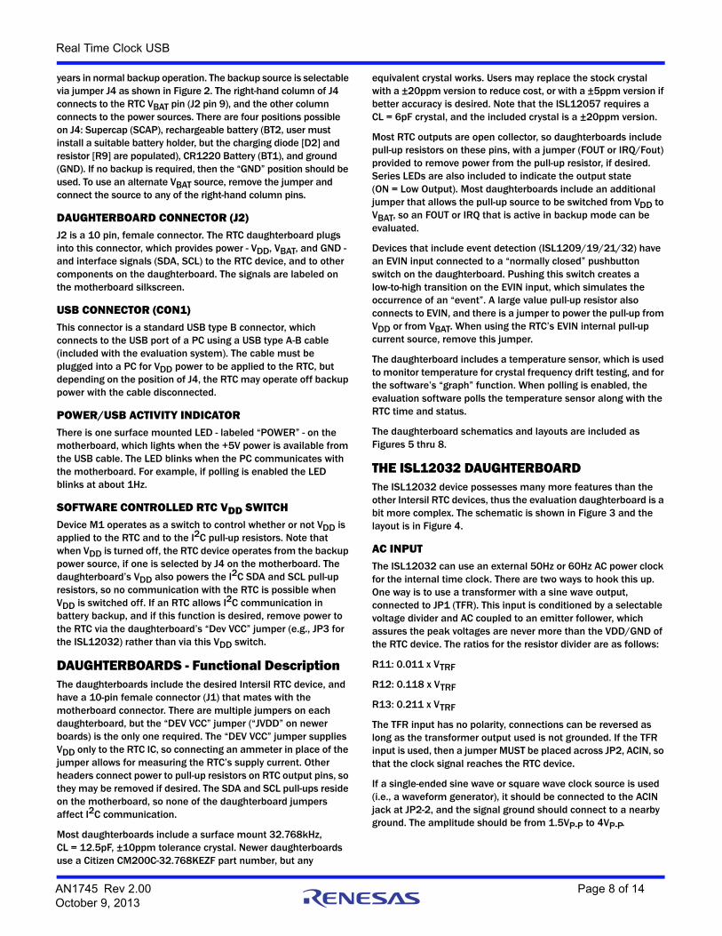
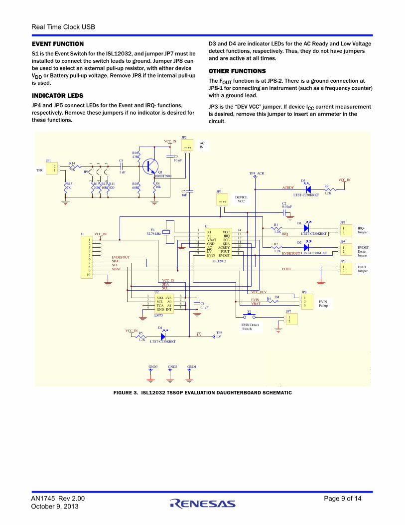
THE ISL12032 DAUGHTERBOARDThe ISL12032 device possesses many more features than the other Intersil RTC devices, thus the evaluation daughterboard is a bit more complex. The schematic is shown in Figure 3 and the layout is in Figure 4.
AC INPUTThe ISL12032 can use an external 50Hz or 60Hz AC power clock for the internal time clock. There are two ways to hook this up. One way is to use a transformer with a sine wave output, connected to JP1 (TFR). This input is conditioned by a selectable voltage divider and AC coupled to an emitter follower, which assures the peak voltages are never more than the VDD/GND of the RTC device. The ratios for the resistor divider are as follows:
R11: 0.011 x VTRF
R12: 0.118 x VTRF
R13: 0.211 x VTRF
The TFR input has no polarity, connections can be reversed as long as the transformer output used is not grounded. If the TFR input is used, then a jumper MUST be placed across JP2, ACIN, so that the clock signal reaches the RTC device.
If a single-ended sine wave or square wave clock source is used (i.e., a waveform generator), it should be connected to the ACIN jack at JP2-2, and the signal ground should connect to a nearby ground. The amplitude should be from 1.5VP-P to 4VP-P.
AN1745 Rev 2.00 Page 8 of 14October 9, 2013
Real Time Clock USB
EVENT FUNCTIONS1 is the Event Switch for the ISL12032, and jumper JP7 must be installed to connect the switch leads to ground. Jumper JP8 can be used to select an external pull-up resistor, with either device VDD or Battery pull-up voltage. Remove JP8 if the internal pull-up is used.
INDICATOR LEDSJP4 and JP5 connect LEDs for the Event and IRQ- functions, respectively. Remove these jumpers if no indicator is desired for these functions.
D3 and D4 are indicator LEDs for the AC Ready and Low Voltage detect functions, respectively. Thus, they do not have jumpers and are active at all times.
OTHER FUNCTIONSThe FOUT function is at JP8-2. There is a ground connection at JP8-1 for connecting an instrument (such as a frequency counter) with a ground lead.
JP3 is the “DEV VCC” jumper. If device ICC current measurement is desired, remove this jumper to insert an ammeter in the circuit..
FIGURE 3. ISL12032 TSSOP EVALUATION DAUGHTERBOARD SCHEMATIC
Title
Size: ReviA
123456789
10
J1
SDASCL
R1
1.2K
VCC_IN
VBAT
12
JP4
C10.1uF
IRQ-Jumper
DEVICEVCC
R2
1.2K12
JP5
EVDETOUT
EVDETDetectJumper
EVIN Detect Switch
SDA1
A0 7
GND4 TCA3 SCL2
A1 6
INT 5
+VS 8U2
LM75
D1
LTST-C230KRKT
D2
LTST-C230KGKT
Y132.76 kHz
ISL12032 TSSOP EVAL DAUGHT
12
JP7
R4 5M 123
JP8
X11
X22
VBAT3
GND4
AC5
LV6
EVIN7 EVDET 8FOUT 9ACRDY 10SDA 11SCL 12IRQ 13VCC 14U1
ISL12032
12
JP6
EVINVBAT
VCC_DEV
12
JP1
R810k
Q1MMBT3904
VCC_IN
VCC_IN
1 2
JP2
IRQ
EVDETOUT
FOUTJumper
C20.01uF
FOUT
D4
LTST-C230KRKT
D3
LTST-C230KRKT
R5
1.2K
LV
R9
1.2K
VCC_IN
VCC_IN
ACRDY
GND1GND2
TP4 ACR
TP5LV
SDASCL
S1
GND3
1 2
JP3
C310 uF
R1643K
R1068K
R11820
R1210K
R1320K
R14
75K
R152K
C4
1 uF
12
34
56
JP9
C51uF
AC IN
TFR
EVINPullup
AN1745 Rev 2.00 Page 9 of 14October 9, 2013
Real Time Clock USB
.
FIGURE 4. ISL12032 DAUGHTERBOARD LAYOUT
AN1745 Rev 2.00 Page 10 of 14October 9, 2013
Real Time Clock USB
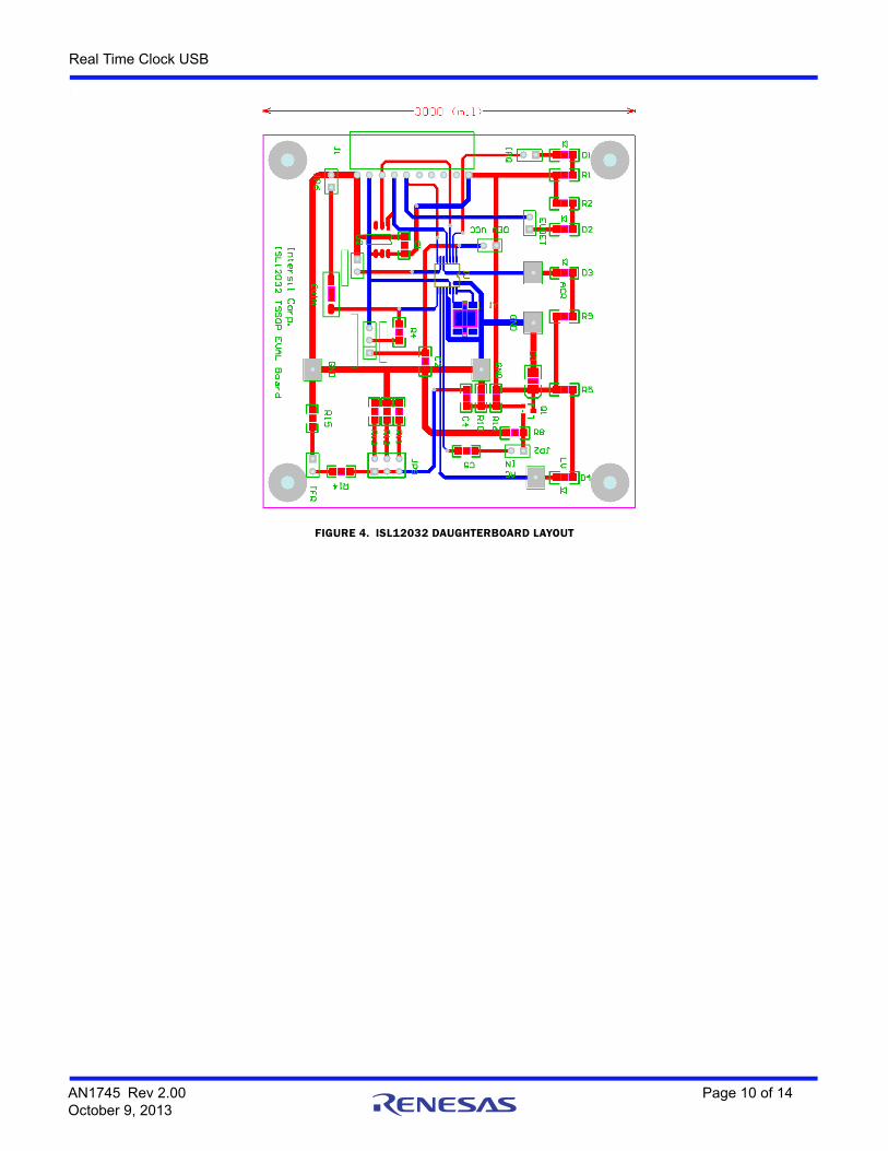
FIGURE 5. ISL12020M/22M EVAL DAUGHTERBOARD SCHEMATIC
JPUSPLY
JVDD
11
12
13
14
15
16
17
18
20
19
10
9
8
7
6
5
4
3
2
1
1
2
3
4
5
6
7
8
9
10
20
19
18
17
16
15
14
13
12
11
123456789
10
J2
1
2
3
4
8
7
6
5
GND
SDASCL
JBAT
VBAT
VDD
JLVRST
D2
D1
R1
1kΩ
R4
1kΩ
IRQ_FOUT
LVRST
C3 C5
C2
C1
LM75
SDA
SDL
C4
ISL12020M
ISL12022M
SDA
SDA
SCL
SCL
R3
0Ω
R5
0Ω
R2
0Ω
ISL12020M = DNP = R2, R3
ISL12022M = DNP = R2, R5
20 LD SOIC
20 LD DFN
1
0.1µF0.1µF
0.1µF
0.1µF
0.1µF
GND
SDA
SCL
VDD
GND
VDD
X1X2
IRQFOUT
IRQ/FOUT
NCNCVBAT
NC
NC
X2
X2
X2
X2
X1
X1
X1
X1
VBAT
NC
NC
NC
NC
NC
GND
NC
NC
NC
NC
NC
NC
NC
GND
VDD
GND
SDA
SDL A0
1
2
OS
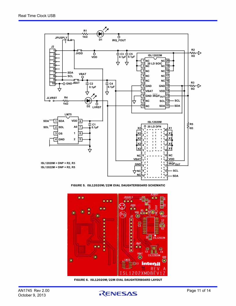
FIGURE 6. ISL12020M/22M EVAL DAUGHTERBOARD LAYOUT
AN1745 Rev 2.00 Page 11 of 14October 9, 2013
Real Time Clock USB
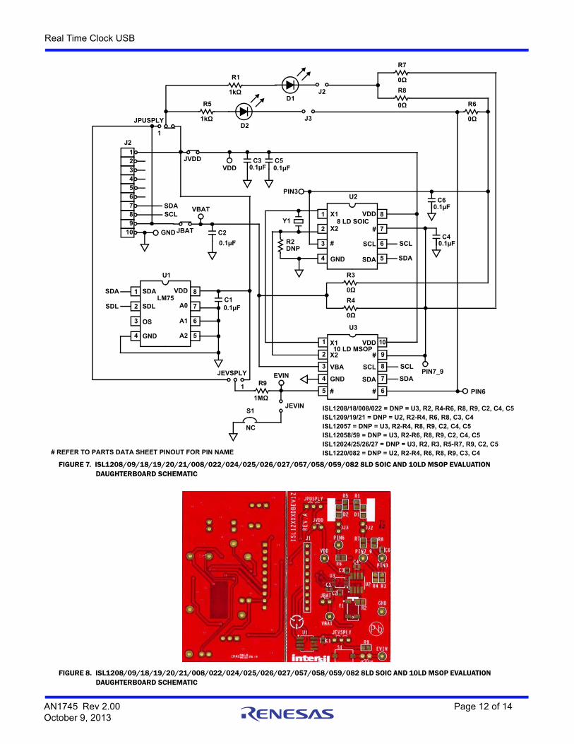
FIGURE 7. ISL1208/09/18/19/20/21/008/022/024/025/026/027/057/058/059/082 8LD SOIC AND 10LD MSOP EVALUATION DAUGHTERBOARD SCHEMATIC
JPUSPLY
JVDD123456789
10
J2
1
2
3
4
8
7
6
5
GND
SDASCL
JBAT
VBAT
VDD
D1
D2
R5
1kΩ
R1
1kΩ
C3 C5
C2
C1
U1
SDA
SDL
C6
SDA
SCL
ISL1208/18/008/022 = DNP = U3, R2, R4-R6, R8, R9, C2, C4, C5
1
2
3
4
8
7
6
5
6
7
8
10
9
5
4
3
2
1
S1
U2
8 LD SOIC
U3
10 LD MSOP
LM75
J3
J2
JEVSPLY
1
1 R9
1MΩJEVIN
NC
EVIN
Y1
R2DNP
SDA
SCL
PIN7_9
PIN3
C4
PIN6
R7
0Ω
R8
0Ω
R3
0Ω
R4
0Ω
0.1µF 0.1µF
0.1µF
0.1µF
0.1µF
R6
0Ω
0.1µF
ISL1209/19/21 = DNP = U2, R2-R4, R6, R8, C3, C4ISL12057 = DNP = U3, R2-R4, R8, R9, C2, C4, C5ISL12058/59 = DNP = U3, R2-R6, R8, R9, C2, C4, C5ISL12024/25/26/27 = DNP = U3, R2, R3, R5-R7, R9, C2, C5ISL1220/082 = DNP = U2, R2-R4, R6, R8, R9, C3, C4
X1
X2
GND SDA
SCL
VDD
#
# REFER TO PARTS DATA SHEET PINOUT FOR PIN NAME
X1
X2
#
GND
VBA
SDA
SCL
VDD
#
#
#
VDD
GND
SDA
SDL A0
A1
A2
OS
FIGURE 8. ISL1208/09/18/19/20/21/008/022/024/025/026/027/057/058/059/082 8LD SOIC AND 10LD MSOP EVALUATION DAUGHTERBOARD SCHEMATIC
AN1745 Rev 2.00 Page 12 of 14October 9, 2013
AN
17
45R
ev 2.0
0P
age
13 of 1
4O
ctober 9, 2013
Rea
l Tim
e C
lock US
B
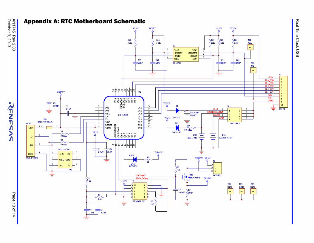
Appendix A: RTC Motherboard Schematic
http://www.renesas.comRefer to "http://www.renesas.com/" for the latest and detailed information.
Renesas Electronics America Inc.1001 Murphy Ranch Road, Milpitas, CA 95035, U.S.A.Tel: +1-408-432-8888, Fax: +1-408-434-5351Renesas Electronics Canada Limited9251 Yonge Street, Suite 8309 Richmond Hill, Ontario Canada L4C 9T3Tel: +1-905-237-2004Renesas Electronics Europe LimitedDukes Meadow, Millboard Road, Bourne End, Buckinghamshire, SL8 5FH, U.KTel: +44-1628-651-700, Fax: +44-1628-651-804Renesas Electronics Europe GmbHArcadiastrasse 10, 40472 Düsseldorf, Germany Tel: +49-211-6503-0, Fax: +49-211-6503-1327Renesas Electronics (China) Co., Ltd.Room 1709 Quantum Plaza, No.27 ZhichunLu, Haidian District, Beijing, 100191 P. R. ChinaTel: +86-10-8235-1155, Fax: +86-10-8235-7679Renesas Electronics (Shanghai) Co., Ltd.Unit 301, Tower A, Central Towers, 555 Langao Road, Putuo District, Shanghai, 200333 P. R. China Tel: +86-21-2226-0888, Fax: +86-21-2226-0999Renesas Electronics Hong Kong LimitedUnit 1601-1611, 16/F., Tower 2, Grand Century Place, 193 Prince Edward Road West, Mongkok, Kowloon, Hong KongTel: +852-2265-6688, Fax: +852 2886-9022Renesas Electronics Taiwan Co., Ltd.13F, No. 363, Fu Shing North Road, Taipei 10543, TaiwanTel: +886-2-8175-9600, Fax: +886 2-8175-9670Renesas Electronics Singapore Pte. Ltd.80 Bendemeer Road, Unit #06-02 Hyflux Innovation Centre, Singapore 339949Tel: +65-6213-0200, Fax: +65-6213-0300Renesas Electronics Malaysia Sdn.Bhd.Unit 1207, Block B, Menara Amcorp, Amcorp Trade Centre, No. 18, Jln Persiaran Barat, 46050 Petaling Jaya, Selangor Darul Ehsan, MalaysiaTel: +60-3-7955-9390, Fax: +60-3-7955-9510Renesas Electronics India Pvt. Ltd.No.777C, 100 Feet Road, HAL 2nd Stage, Indiranagar, Bangalore 560 038, IndiaTel: +91-80-67208700, Fax: +91-80-67208777Renesas Electronics Korea Co., Ltd.17F, KAMCO Yangjae Tower, 262, Gangnam-daero, Gangnam-gu, Seoul, 06265 KoreaTel: +82-2-558-3737, Fax: +82-2-558-5338
SALES OFFICES
© 2018 Renesas Electronics Corporation. All rights reserved.Colophon 7.0
(Rev.4.0-1 November 2017)
Notice
1. Descriptions of circuits, software and other related information in this document are provided only to illustrate the operation of semiconductor products and application examples. You are fully responsible for
the incorporation or any other use of the circuits, software, and information in the design of your product or system. Renesas Electronics disclaims any and all liability for any losses and damages incurred by
you or third parties arising from the use of these circuits, software, or information.
2. Renesas Electronics hereby expressly disclaims any warranties against and liability for infringement or any other claims involving patents, copyrights, or other intellectual property rights of third parties, by or
arising from the use of Renesas Electronics products or technical information described in this document, including but not limited to, the product data, drawings, charts, programs, algorithms, and application
examples.
3. No license, express, implied or otherwise, is granted hereby under any patents, copyrights or other intellectual property rights of Renesas Electronics or others.
4. You shall not alter, modify, copy, or reverse engineer any Renesas Electronics product, whether in whole or in part. Renesas Electronics disclaims any and all liability for any losses or damages incurred by
you or third parties arising from such alteration, modification, copying or reverse engineering.
5. Renesas Electronics products are classified according to the following two quality grades: “Standard” and “High Quality”. The intended applications for each Renesas Electronics product depends on the
product’s quality grade, as indicated below.
"Standard": Computers; office equipment; communications equipment; test and measurement equipment; audio and visual equipment; home electronic appliances; machine tools; personal electronic
equipment; industrial robots; etc.
"High Quality": Transportation equipment (automobiles, trains, ships, etc.); traffic control (traffic lights); large-scale communication equipment; key financial terminal systems; safety control equipment; etc.
Unless expressly designated as a high reliability product or a product for harsh environments in a Renesas Electronics data sheet or other Renesas Electronics document, Renesas Electronics products are
not intended or authorized for use in products or systems that may pose a direct threat to human life or bodily injury (artificial life support devices or systems; surgical implantations; etc.), or may cause
serious property damage (space system; undersea repeaters; nuclear power control systems; aircraft control systems; key plant systems; military equipment; etc.). Renesas Electronics disclaims any and all
liability for any damages or losses incurred by you or any third parties arising from the use of any Renesas Electronics product that is inconsistent with any Renesas Electronics data sheet, user’s manual or
other Renesas Electronics document.
6. When using Renesas Electronics products, refer to the latest product information (data sheets, user’s manuals, application notes, “General Notes for Handling and Using Semiconductor Devices” in the
reliability handbook, etc.), and ensure that usage conditions are within the ranges specified by Renesas Electronics with respect to maximum ratings, operating power supply voltage range, heat dissipation
characteristics, installation, etc. Renesas Electronics disclaims any and all liability for any malfunctions, failure or accident arising out of the use of Renesas Electronics products outside of such specified
ranges.
7. Although Renesas Electronics endeavors to improve the quality and reliability of Renesas Electronics products, semiconductor products have specific characteristics, such as the occurrence of failure at a
certain rate and malfunctions under certain use conditions. Unless designated as a high reliability product or a product for harsh environments in a Renesas Electronics data sheet or other Renesas
Electronics document, Renesas Electronics products are not subject to radiation resistance design. You are responsible for implementing safety measures to guard against the possibility of bodily injury, injury
or damage caused by fire, and/or danger to the public in the event of a failure or malfunction of Renesas Electronics products, such as safety design for hardware and software, including but not limited to
redundancy, fire control and malfunction prevention, appropriate treatment for aging degradation or any other appropriate measures. Because the evaluation of microcomputer software alone is very difficult
and impractical, you are responsible for evaluating the safety of the final products or systems manufactured by you.
8. Please contact a Renesas Electronics sales office for details as to environmental matters such as the environmental compatibility of each Renesas Electronics product. You are responsible for carefully and
sufficiently investigating applicable laws and regulations that regulate the inclusion or use of controlled substances, including without limitation, the EU RoHS Directive, and using Renesas Electronics
products in compliance with all these applicable laws and regulations. Renesas Electronics disclaims any and all liability for damages or losses occurring as a result of your noncompliance with applicable
laws and regulations.
9. Renesas Electronics products and technologies shall not be used for or incorporated into any products or systems whose manufacture, use, or sale is prohibited under any applicable domestic or foreign laws
or regulations. You shall comply with any applicable export control laws and regulations promulgated and administered by the governments of any countries asserting jurisdiction over the parties or
transactions.
10. It is the responsibility of the buyer or distributor of Renesas Electronics products, or any other party who distributes, disposes of, or otherwise sells or transfers the product to a third party, to notify such third
party in advance of the contents and conditions set forth in this document.
11. This document shall not be reprinted, reproduced or duplicated in any form, in whole or in part, without prior written consent of Renesas Electronics.
12. Please contact a Renesas Electronics sales office if you have any questions regarding the information contained in this document or Renesas Electronics products.
(Note 1) “Renesas Electronics” as used in this document means Renesas Electronics Corporation and also includes its directly or indirectly controlled subsidiaries.
(Note 2) “Renesas Electronics product(s)” means any product developed or manufactured by or for Renesas Electronics.