RE46C165/6/7/8 CMOS Photoelectric Smoke Detector...
30
2010-2016 Microchip Technology Inc. DS20002251B-page 1 RE46C165/6/7/8 Features • Temporal Horn Pattern or Continuous Tone • Alarm Memory • Sensitivity Control Times: - 9 minutes (RE46C165/6) - 1.2 minutes (RE46C167/8) • I/O Filter and Charge Dump • Interconnect up to 40 Detectors • Internal Power-on Reset (POR) • >2000V ESD Protection (HBM) on All Pins • Low Quiescent Current Consumption (<8 μA) • Internal Low Battery Detection and Chamber Test • RoHS Compliant Lead-Free Packaging Description The RE46C165/6/7/8 devices are low-power, CMOS photoelectric type, smoke detector ICs. With minimal external components, these circuits will provide all the required features for a photoelectric type smoke detector. Each design incorporates a gain-selectable photo amplifier for use with an infrared emitter/detector pair. An internal oscillator strobes power to the smoke detection circuitry for 100 μs, every 10 seconds, to keep standby current to a minimum. If smoke is sensed, the detection rate is increased to verify an alarm condition. A High-Gain mode is available for push button chamber testing. A check for a low battery condition and chamber integrity is performed every 43 seconds when in standby. The temporal horn pattern supports the NFPA 72 emergency evacuation signal. An interconnect pin allows multiple detectors to be connected so when one unit alarms, all units will sound. A charge dump feature will quickly discharge the interconnect line when exiting a local alarm. The interconnect input is also digitally filtered. An internal timer allows for single button, push-to-test to be used for a Reduced Sensitivity mode. An alarm memory feature allows the user to determine if the unit has previously entered a local alarm condition. Utilizing low-power CMOS technology, the RE46C165/6/7/8 was designed for use in smoke detectors that comply with Underwriters Laboratory Specification UL217 and UL268. CMOS Photoelectric Smoke Detector ASIC with Interconnect, Timer Mode and Alarm Memory
Transcript of RE46C165/6/7/8 CMOS Photoelectric Smoke Detector...

RE46C165/6/7/8CMOS Photoelectric Smoke Detector ASIC
with Interconnect, Timer Mode and Alarm Memory
Features
• Temporal Horn Pattern or Continuous Tone
• Alarm Memory
• Sensitivity Control Times:
- 9 minutes (RE46C165/6)
- 1.2 minutes (RE46C167/8)
• I/O Filter and Charge Dump
• Interconnect up to 40 Detectors
• Internal Power-on Reset (POR)
• >2000V ESD Protection (HBM) on All Pins
• Low Quiescent Current Consumption (<8 µA)
• Internal Low Battery Detection and Chamber Test
• RoHS Compliant Lead-Free Packaging
Description
The RE46C165/6/7/8 devices are low-power, CMOSphotoelectric type, smoke detector ICs. With minimalexternal components, these circuits will provide all therequired features for a photoelectric type smokedetector.
Each design incorporates a gain-selectable photoamplifier for use with an infrared emitter/detector pair.
An internal oscillator strobes power to the smokedetection circuitry for 100 µs, every 10 seconds, tokeep standby current to a minimum. If smoke issensed, the detection rate is increased to verify analarm condition. A High-Gain mode is available forpush button chamber testing.
A check for a low battery condition and chamberintegrity is performed every 43 seconds when instandby. The temporal horn pattern supports theNFPA 72 emergency evacuation signal.
An interconnect pin allows multiple detectors to beconnected so when one unit alarms, all units will sound.A charge dump feature will quickly discharge theinterconnect line when exiting a local alarm. Theinterconnect input is also digitally filtered.
An internal timer allows for single button, push-to-testto be used for a Reduced Sensitivity mode.
An alarm memory feature allows the user to determineif the unit has previously entered a local alarmcondition.
Utilizing low-power CMOS technology, theRE46C165/6/7/8 was designed for use in smokedetectors that comply with Underwriters LaboratorySpecification UL217 and UL268.
2010-2016 Microchip Technology Inc. DS20002251B-page 1
RE46C165/6/7/8
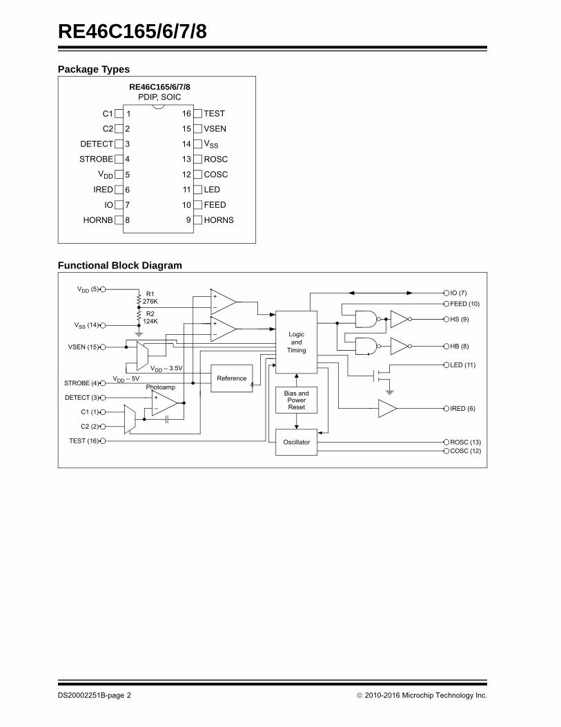
Package Types
Functional Block Diagram
RE46C165/6/7/8 PDIP, SOIC
C1 1
2
3
4
5
6
7
8
16
15
14
13
12
11
10
9
C2
DETECT
STROBE
VDD
IRED
IO
HORNB
TEST
VSEN
VSS
ROSC
COSC
LED
FEED
HORNS
Logicand
Timing
Bias andPowerReset
+
–
+
–
VDD (5)
VSEN (15)
C1 (1)
DETECT (3)
C2 (2)
TEST (16)
R2124K
R1276K
IO (7)
FEED (10)
HS (9)
LED (11)
IRED (6)
ROSC (13)COSC (12)
HB (8)
+
–
STROBE (4)VDD – 5V
VDD – 3.5V
Photoamp
VSS (14)
Reference
Oscillator
DS20002251B-page 2 2010-2016 Microchip Technology Inc.
RE46C165/6/7/8
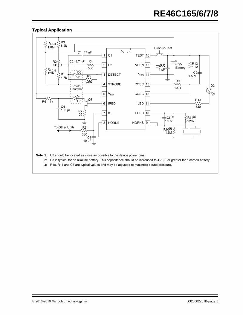
Typical Application
Push-to-Test
9VBatteryC3(1,2)
1 µFC5
1.5 nF
R1210M
R9
100k
R13
330
D3
C6(3)
1.0 nF
R10(3)
1.5M
R11(3)
220k
R8
330C7
10 µF
R722
C4100 µF
D5
D6
R4
560
C2 4.7 nF
C1 47 nF
R14.7k
R25k
R38.2k
RADJ2120k
RADJ11.0M
R6 1k
C1
C2
DETECT
STROBE
VDD
VSS
IRED
IO
HORNB HORNS
FEED
LED
COSC
ROSC
VSEN
TEST
R5
249k
To Other Units
1
2
3
4
5
6
7
8
16
15
14
13
12
11
10
9
Note 1: C3 should be located as close as possible to the device power pins.
2: C3 is typical for an alkaline battery. This capacitance should be increased to 4.7 µF or greater for a carbon battery.
3: R10, R11 and C6 are typical values and may be adjusted to maximize sound pressure.
Q3
PhotoChamber
2010-2016 Microchip Technology Inc. DS20002251B-page 3

RE46C165/6/7/8
NOTES:
DS20002251B-page 4 2010-2016 Microchip Technology Inc.

RE46C165/6/7/8
1.0 ELECTRICAL CHARACTERISTICS
Absolute Maximum Ratings†
VDD ...................................................................................12.5VInput Voltage Range except FEED, I/O......VIN = -0.3V to VDD + 0.3VFEED Input Voltage Range....................... VINFD = -10 to +22VI/O Input Voltage Range..................................VIO1= -0.3 to 15VInput Current except FEED, TEST, VSEN ............... IIN = 10 mAInput Current for FEED, VSEN ............................... IIN = 500 µAOperating Temperature...................................TA = -25 to +75°CStorage Temperature ...............................TSTG = -55 to +125°CMaximum Junction Temperature............................ TJ = +150°C
† Notice: Stresses above those listed under “MaximumRatings” may cause permanent damage to the device.This is a stress rating only and functional operation ofthe device at these, or any other conditions above thoseindicated in the operation listings of this specification, isnot implied. Exposure to maximum rating conditions forextended periods may affect device reliability.
DC ELECTRICAL CHARACTERISTICS(3)
DC Electrical Characteristics: Unless otherwise indicated, all parameters apply at TA = -25° to +75°, VDD = 9V, Typical Application (unless otherwise noted), VSS = 0V
Parameter Symbol Test Pin Min. Typ. Max. Units Conditions
Supply Voltage VDD 5 6 — 12 V Operating
Supply Current IDD1 5 — 4 6 µA COSC = VSS, LED off
IDD2 5 — 5.5 8 µA COSC = VSS, LED off, VDD = 12V
IDD3 5 — — 2 mA COSC = VSS, STROBE on IRED off
IDD4 5 — — 3 mA COSC = VSS, STROBE on, IRED on (Note 1)
Input Voltage High VIH1 10 6.2 4.5 — V FEED
VIH2 7 3.2 — — V No local alarm, I/O as an input
VIH3 15 1.6 — — V VSEN
VIH4 16 8.5 — — V TEST
Input Voltage Low VIL1 10 — 4.5 2.7 V FEED
VIL2 7 — — 1.5 V No local alarm, I/O as an input
VIL3 15 — — 0.5 V VSEN
VIL4 16 — — 7 V TEST
Input Leakage Low IIL1 1, 2, 3 — — -100 nA VDD = 12V, COSC = 12V, STROBE active
IIL2 12, 10 — — -100 nA VDD = 12V, VIN = VSS
IIL3 15, 16 — — -1 µA VDD = 12V, VIN = VSS
ILFD 10 — — -50 µA FEED = -10V
Input Leakage High IIH1 1, 2 — — 100 nA VDD = 12V, VIN = VDD, STROBE active
IIH2 3, 10, 12 — — 100 nA VDD = 12V, VIN = VDD
IHFD 10 — — 50 µA FEED = 22V
Note 1: Does not include Q3 emitter current.
2: Not production tested.
3: Production tested at room temperature with guardbanded limits.
2010-2016 Microchip Technology Inc. DS20002251B-page 5

RE46C165/6/7/8
Input Pull-Down Current
IPD1 16 0.25 — 10 µA VIN = VDD
IPD2 15 0.1 0.25 0.5 µA VIN = VDD
IPDIO1 7 20 — 80 µA VIN = VDD
IPDIO2 7 — — 140 µA VIN = 15V, VDD = 12V
Output Off Leakage Low
IOZL1 11, 13 — — -1 µA Outputs off, Output = VSS
Output Off Leakage High
IOZH1 11, 13 — — 1 µA Outputs off, Output = VDD
Output High Voltage VOH1 8, 9 5.5 — — V IOH = -16 mA, VDD = 6.5V
Output Low Voltage VOL1 8, 9 — — 1 V IOL = 16 mA, VDD = 6.5V
VOL2 13 — 0.5 — V IOL = 5 mA, VDD = 6.5V
VOL3 11 — — 0.6 V IOL = 10 mA, VDD = 6.5V
Output Current IIOH1 7 -4 — -16 mA Alarm, VIO = VDD – 2V or VIO = 0V
IIODMP 7 5 — — mA At conclusion of local alarm or test, VIO = 1V
Low Battery Voltage VLB 5 6.9 7.2 7.5 V
Output Voltage VSTOF 4 VDD – 0.1 — — V STROBE off, VDD = 12V, IOUT = -1 µA
VSTON 4 VDD – 5.25 VDD – 5 VDD – 4.75 V STROBE on, VDD = 9V, IOUT = 100 µA to 500 µA
VIREDOF 6 — — 0.1 V IRED off, VDD = 12V, IOUT = 1 µA
VIREDON 6 2.85 3.1 3.35 V IRED on, VDD = 9V,IOUT = 0 to -6 mA, TA = +25°C
Common-Mode Voltage
VCM1 1, 2, 3 0.5 — VDD – 2 V Local smoke, push-to-test or chamber test (Note 2)
Smoke Comparator Reference
VREF — VDD – 3.7 VDD – 3.5 VDD – 3.3 V Internal reference (Note 2)
Temperature Coefficient
TCST 4 — 0.01 — %/°C STROBE output voltage, VDD = 6V to 12V
TCIRED 6 — 0.3 — %/°C IRED output voltage, VDD = 6V to 12V
Line Regulation VSTON 4, 5 — -50 — dB STROBE output (vs. VDD), VDD = 6V to 12V
VIREDON 6, 5 — -30 — dB IRED output voltage, VDD = 6V to 12V
DC ELECTRICAL CHARACTERISTICS(3) (CONTINUED)
DC Electrical Characteristics: Unless otherwise indicated, all parameters apply at TA = -25° to +75°, VDD = 9V, Typical Application (unless otherwise noted), VSS = 0V
Parameter Symbol Test Pin Min. Typ. Max. Units Conditions
Note 1: Does not include Q3 emitter current.
2: Not production tested.
3: Production tested at room temperature with guardbanded limits.
DS20002251B-page 6 2010-2016 Microchip Technology Inc.

RE46C165/6/7/8
AC ELECTRICAL CHARACTERISTICS
AC Electrical Characteristics: Unless otherwise indicated, all parameters apply at TA = -25° to +75°, VDD = 9V, Typical Application (unless otherwise noted), VSS = 0V.
Parameter SymbolTest Pin
Min. Typ. Max. Units Clocks Conditions
Oscillator Time Base (COSC, ROSC)
Oscillator Period TPOSC 9 9.38 10.42 11.46 ms 1 Operating (Note 1)
Oscillator Tolerance TTOLOSC 9 -10 0 10 % 1 Operating
LED Indication (LED)
LED On Time TON1 11 9.4 10.4 11.5 ms 1 Operating
LED Period TPLED0 11 LED IS NOT ON s — Remote alarm only
TPLED1 11 38 43 47 s 4096 Standby, no alarm
TPLED2 11 450 500 550 ms 48 Local alarm condition
TPLED3 11 9.6 10.7 11.7 s 1024 Timer mode, no local alarm (Note 4)
TPLED4 11 225 250 275 ms 24 Timer mode, no local alarm (Note 4)
Alarm Memory LEDPulse Train (3x) Off Time
TOFLED 11 1.2 1.3 1.5 s 127 Alarm memory set, LED enabled
Alarm Memory LED Timer Period
TLALED 11 21.5 23.9 26.3 Hours 8257536 Alarm memory set
Detection (STROBE, IRED)
STROBE On Time TSTON 4 9.4 10.4 11.5 ms 1 Smoke test, chamber test
IRED On Time TIRON 6 94 104 114 µs 0.01 Operating/DIAG (Note 1)
Note 1: TPOSC and TIRON are 100% production tested. All other timing is verified by functional testing.
2: See the timing diagram for Horn Temporal Pattern in Figure 3-2.
3: See the timing diagram for Horn Continuous Pattern in Figure 3-3.
4: During Timer mode, the LED period is 10.5 seconds. The LED period will return to 43 seconds at the conclusion of the Timer mode.
2010-2016 Microchip Technology Inc. DS20002251B-page 7
RE46C165/6/7/8
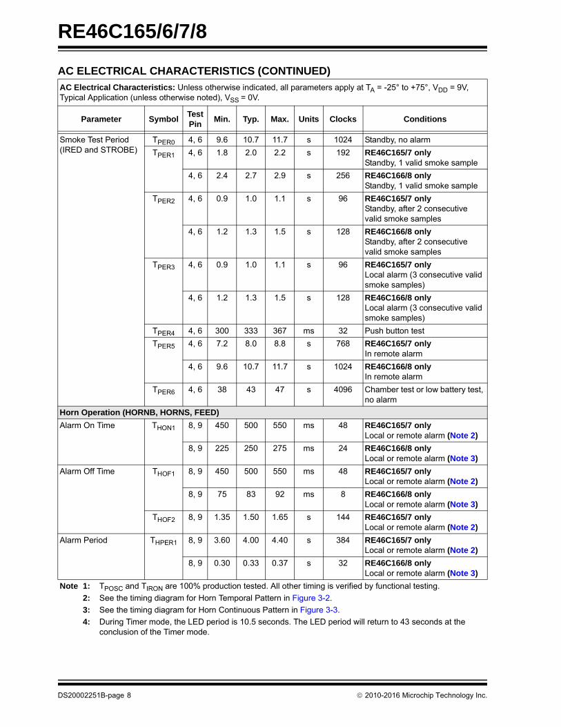
Smoke Test Period(IRED and STROBE)
TPER0 4, 6 9.6 10.7 11.7 s 1024 Standby, no alarm
TPER1 4, 6 1.8 2.0 2.2 s 192 RE46C165/7 onlyStandby, 1 valid smoke sample
4, 6 2.4 2.7 2.9 s 256 RE46C166/8 onlyStandby, 1 valid smoke sample
TPER2 4, 6 0.9 1.0 1.1 s 96 RE46C165/7 only Standby, after 2 consecutive valid smoke samples
4, 6 1.2 1.3 1.5 s 128 RE46C166/8 only Standby, after 2 consecutive valid smoke samples
TPER3 4, 6 0.9 1.0 1.1 s 96 RE46C165/7 only Local alarm (3 consecutive valid smoke samples)
4, 6 1.2 1.3 1.5 s 128 RE46C166/8 only Local alarm (3 consecutive valid smoke samples)
TPER4 4, 6 300 333 367 ms 32 Push button test
TPER5 4, 6 7.2 8.0 8.8 s 768 RE46C165/7 onlyIn remote alarm
4, 6 9.6 10.7 11.7 s 1024 RE46C166/8 onlyIn remote alarm
TPER6 4, 6 38 43 47 s 4096 Chamber test or low battery test, no alarm
Horn Operation (HORNB, HORNS, FEED)
Alarm On Time THON1 8, 9 450 500 550 ms 48 RE46C165/7 onlyLocal or remote alarm (Note 2)
8, 9 225 250 275 ms 24 RE46C166/8 onlyLocal or remote alarm (Note 3)
Alarm Off Time THOF1 8, 9 450 500 550 ms 48 RE46C165/7 onlyLocal or remote alarm (Note 2)
8, 9 75 83 92 ms 8 RE46C166/8 onlyLocal or remote alarm (Note 3)
THOF2 8, 9 1.35 1.50 1.65 s 144 RE46C165/7 onlyLocal or remote alarm (Note 2)
Alarm Period THPER1 8, 9 3.60 4.00 4.40 s 384 RE46C165/7 onlyLocal or remote alarm (Note 2)
8, 9 0.30 0.33 0.37 s 32 RE46C166/8 onlyLocal or remote alarm (Note 3)
AC ELECTRICAL CHARACTERISTICS (CONTINUED)
AC Electrical Characteristics: Unless otherwise indicated, all parameters apply at TA = -25° to +75°, VDD = 9V, Typical Application (unless otherwise noted), VSS = 0V.
Parameter SymbolTest Pin
Min. Typ. Max. Units Clocks Conditions
Note 1: TPOSC and TIRON are 100% production tested. All other timing is verified by functional testing.
2: See the timing diagram for Horn Temporal Pattern in Figure 3-2.
3: See the timing diagram for Horn Continuous Pattern in Figure 3-3.
4: During Timer mode, the LED period is 10.5 seconds. The LED period will return to 43 seconds at the conclusion of the Timer mode.
DS20002251B-page 8 2010-2016 Microchip Technology Inc.

RE46C165/6/7/8
Low Battery or Chamber Fail Horn On Time
THON2 8, 9 9.4 10.4 11.5 ms 1 Low battery or fail chamber test, no alarm
Low Battery Horn Off Time
THOF3 8, 9 38 43 47 s 4095 Low battery, no alarm
Low Battery or Chamber Fail Period
THPER2 8, 9 38 43 47 s 4096 Low battery, no alarm
Chamber Fail Horn Off Time
THOF4 8, 9 291 323 355 ms 31 Failed chamber, no alarm
Chamber Fail Pause Off Time
THOF5 8, 9 38 42 46 s 4031 Failed chamber, no alarm
Push-to-Test Alarm Memory Off Time
THOF6 8, 9 216 240 264 ms 23 Alarm memory active, push-to-test
Push-to-Test Alarm Memory Period
THPER3 8, 9 225 250 275 ms 24 Alarm memory active, push-to-test
Interconnect Signal Operation (I/O)
I/O Active Delay TIODLY1 7 0.0 0.0 0.0 s 0 Local alarm start to I/O active
Remote Alarm Delay TIODLY2 7 0.74 0.99 1.27 s 95 RE46C165/7 onlyNo local alarm, I/O active to alarm
7 0.37 0.57 0.81 s 55 RE46C166/8 onlyNo local alarm, I/O active to alarm
I/O Charge Dump Duration
TIODMP 7 0.89 0.99 1.09 s 95 RE46C165/7 onlyAt conclusion of local alarm or test
7 1.19 1.32 1.46 s 127 RE46C166/8 onlyAt conclusion of local alarm or test
I/O Filter TIOFILT 7 — — 0.30 s 32 Maximum I/O pulse width filtered
Hush Timer Operation
Hush Timer Period TTPER — 8.1 9.0 9.9 Min 51712 RE46C165/6 onlyNo alarm condition
— 1.1 1.2 1.4 Min 7232 RE46C167/8 onlyNo alarm condition
AC ELECTRICAL CHARACTERISTICS (CONTINUED)
AC Electrical Characteristics: Unless otherwise indicated, all parameters apply at TA = -25° to +75°, VDD = 9V, Typical Application (unless otherwise noted), VSS = 0V.
Parameter SymbolTest Pin
Min. Typ. Max. Units Clocks Conditions
Note 1: TPOSC and TIRON are 100% production tested. All other timing is verified by functional testing.
2: See the timing diagram for Horn Temporal Pattern in Figure 3-2.
3: See the timing diagram for Horn Continuous Pattern in Figure 3-3.
4: During Timer mode, the LED period is 10.5 seconds. The LED period will return to 43 seconds at the conclusion of the Timer mode.
2010-2016 Microchip Technology Inc. DS20002251B-page 9

RE46C165/6/7/8
TEMPERATURE CHARACTERISTICS
Electrical Specifications: Unless otherwise indicated, VDD = 9V, Typical Application (unless otherwise noted), VSS = 0V
Parameters Sym. Min. Typ. Max. Units Conditions
Temperature Ranges
Specified Temperature Range TA -25 — +75 °C
Operating Temperature Range TA -25 — +75 °C
Storage Temperature Range TSTG -55 — +125 °C
Thermal Package Resistances
Thermal Resistance, 16L-PDIP θJA — 70 — °C/W
Thermal Resistance, 16L-SOIC (150 mil) θJA — 86.1 — °C/W
DS20002251B-page 10 2010-2016 Microchip Technology Inc.

RE46C165/6/7/8
2.0 PIN DESCRIPTIONS
The descriptions of the pins are listed in Table 2-1.
2.1 High/Normal Gain Capacitor Pins (C1, C2)
The capacitor connected to the C1 pin sets the photoamplifier gain (high) for the push-to-test and chambersensitivity test. The size of this capacitor will depend onthe chamber background reflections. A = 1 + (C1/10),where C1 is expressed in pF. The gain should be<10000.
The capacitor connected to the C2 pin sets the photoamplifier gain (normal) during standby. The value of thiscapacitor will depend on the smoke sensitivity required.A = 1 + (C2/10), where C2 is expressed in pF.
2.2 Photo Diode Input (DETECT)
This input is normally connected to the cathode of anexternal photo diode operated at zero bias.
2.3 Strobed Detection Negative Supply (STROBE)
Regulated output voltage of VDD – 5, which is activeduring a test for smoke. This output is the negative sideof the photo amplifier reference circuitry.
2.4 Positive Power Supply (VDD)
The VDD pin is the device’s positive power supply input.
2.5 Infrared Emitting Diode Pin (IRED)
Provides a regulated pulsed output voltage pre-driverfor the infrared emitter. This output usually drives thebase of an NPN transistor.
2.6 Interconnect Pin (I/O)
This bidirectional pin provides the capability tointerconnect many detectors in a single system. Thispin has an internal pull-down device.
2.7 Horn Brass, Inverted Output (HB)
The HB pin is connected to the metal electrode of apiezoelectric transducer.
2.8 Horn Silver Output Pin (HS)
The HS pin is a complementary output to HB andconnects to the ceramic electrode of the piezoelectrictransducer.
TABLE 2-1: PIN FUNCTION TABLE
RE46C165/6/7/8PDIP, SOIC
Symbol Function
1 C1 High-Gain Capacitor Pin
2 C2 Normal Gain Capacitor Pin
3 DETECT Photo Diode Input
4 STROBE Strobed Detection Negative Supply
5 VDD Positive Power Supply
6 IRED Infrared Emitting Diode Pin
7 IO Interconnect Pin
8 HB Horn Brass, Inverted Output
9 HS Horn Silver Output
10 FEED Horn Feedback Pin
11 LED LED Driver Pin
12 COSC Oscillator Capacitor Input
13 ROSC Oscillator Resistor Drive Low
14 VSS Negative Power Supply
15 VSEN Hush Timer Sensitivity Pin
16 TEST Test Pin
2010-2016 Microchip Technology Inc. DS20002251B-page 11
RE46C165/6/7/8
2.9 Horn Feedback Pin (FEED)
Usually, this pin is connected to the feedback electrodethrough a current-limiting resistor. If not used, this pinmust be connected to VDD or VSS.
When the horn is enabled, FEED drives the bufferedoutput HS pin and the complementary output HB pin.
2.10 LED Driver Pin (LED)
This pin is an open-drain NMOS output used to drive avisible LED.
2.11 Oscillator Capacitor Input (COSC)
A capacitor connected to this pin, with a parallelresistor, sets the internal clock low time, which isapproximately the clock period.
2.12 Oscillator Resistor Drive Low (ROSC)
A resistor between this pin and the COSC pin sets theinternal clock high time. This also sets the IRED pulsewidth.
2.13 Hush Timer Sensitivity Pin (VSEN)
In Timer mode, this input pin can be used to set anexternal smoke comparator reference.
2.14 TEST Pin
This input is used to invoke two Test modes and theTimer mode. This input has an internal pull-down.
DS20002251B-page 12 2010-2016 Microchip Technology Inc.

RE46C165/6/7/8
3.0 DEVICE DESCRIPTION
3.1 Internal Timing
With the external components specified in the TypicalApplication section for ROSC and COSC, the internaloscillator has a nominal period of 10 ms. Normally, theanalog circuitry is powered down to minimize standbycurrent (typically 4 µA at 9V). Once every 10 seconds,the detection circuitry (normal gain) is powered upfor 10 ms. Prior to completion of the 10 ms period, theIRED pulse is active for 100 µs. At the conclusion of the10 ms period, the photo amplifier is compared to aninternal reference to determine the chamber status andlatched. If a smoke condition is present, the period tothe next detection decreases and additional checks aremade. Three consecutive smoke detections will causethe device to go into alarm, and the horn circuit andinterconnect will be active.
Once every 43 seconds, the status of the battery volt-age is checked. This status is checked and latched atthe conclusion of the LED pulse. In addition, onceevery 43 seconds, the chamber is activated, and usingthe High-Gain mode (capacitor C1), a check of thechamber is made by amplifying background reflections.If either the low battery or the photo chamber test fails,the horn will chirp for 10 ms every 43 seconds.
The oscillator period is determined by the values of R9,R12 and C5 (see the Typical Application figure). Theoscillator period is as follows:
EQUATION 3-1:
3.2 Smoke Detection Circuit
A comparator compares the photo amplifier output to aninternal reference voltage. If the required number of con-secutive smoke conditions is met, the device will go intolocal alarm and the horn will be active. In local alarm, theC2 gain is internally increased by approximately 10% toprovide alarm hysteresis.
3.3 Push-to-Test Operation
If the TEST input pin is activated (VIH4), the smoke detec-tion is sampled at a high rate. The RE46C166/8 devicessample at a period of 330 ms. The RE46C165/7 deviceshave a first sample delay of up to 330 ms. After onesample, the smoke detection rate increases to onceevery 250 ms. In this mode, the high-gain capacitor C1 isselected and background reflections are used to simulatea smoke condition. After the required three consecutive
detections, the device will go into a local alarm condition.When the TEST input is deactivated (VIL4) and after oneclock cycle, the normal gain capacitor C2 is selected. Thedetection rate continues, once every 330 ms for theRE46C166/8, and every 250 ms while the horn is notsounding for the RE46C165/7. When three consecutive‘no smoke’ conditions are detected, the device returns tostandby timing.
Push-to-test will not work while the alarm memory isset. The alarm memory notification will be activatedinstead.
3.4 LED Pulse
In standby, the LED is pulsed on for 10 ms, every43 seconds. In a local alarm condition, or thepush-to-test alarm, the LED pulse frequency isincreased once every 0.5 seconds. In the case of aremote alarm, the LED is not active. In the Timer modeof operation, the LED is pulsed on for 10 ms every10 seconds.
3.5 Interconnect
The bidirectional I/O pin allows the interconnection ofmultiple detectors. In a local alarm condition, this pin isdriven high immediately through a constant-currentsource. Shorting this output to ground will not causeexcessive current. The I/O is ignored as an input duringa local alarm.
The I/O pin has a 280k nominal pull-down resistor, sothe pin may be left unconnected.
The I/O pin also has an NMOS discharge device that isactive for 1 second after the conclusion of any type oflocal alarm. This device helps to quickly discharge anycapacitance associated with the interconnect line.
If a remote active-high signal is detected, the devicegoes into remote alarm and the horn will be active.Internal protection circuitry allows for the signaling unitto have a higher supply voltage than the signaled unit,without excessive current draw.
The interconnect input has a digital filter that ensuresfiltering out pulses of up to 300 ms. Filter pulses will beignored and not affect internal timing of the part. Thisallows for interconnection to other types of alarms (car-bon monoxide, for example) that may have a pulsedinterconnect signal.
The remote alarm delay (370 ms to 1.27s) specifies thetime from the interconnect going active to sounding thepiezo horn alarm.
T = TR + TF
Where:
TR = 0.693 * R12 * C5
TF = 0.693 * R9 * C5
2010-2016 Microchip Technology Inc. DS20002251B-page 13

RE46C165/6/7/8
3.6 Low Battery Detection
In standby, an internal reference is compared to thevoltage divided VDD supply. A low battery status islatched at the conclusion of the LED pulse. The hornwill chirp once for 10 ms, every 43 seconds, until thelow battery condition no longer exists. The low batterychirp occurs next to the LED pulse.
The low battery notification does not sound in a local orremote alarm condition.
3.7 Chamber Fail Detection
In standby, a chamber test is also performed every43 seconds by switching to the high-gain capacitor C1and sensing the photo chamber background reflec-tions. Two consecutive chamber test failures will causethe horn to chirp 3 times for 10 ms, spaced 323 msapart. This will repeat every 42 seconds, as long as achamber test fail exists. The failed chamber test chirpsoccur ~21 seconds after the LED pulse in Standbymode (not hush).
The chamber fail notification does not sound in a localor remote alarm condition.
3.8 Timer Mode
If resistors, RADJ1 and RADJ2 (see Typical Applicationfigure), are in place and a high-to-low transition occurson the TEST input, the device enters a Timer mode(10 minutes maximum for RE46C165/6 devices,1 minute maximum for RE46C167/8). In this mode, thesmoke comparator reference is switched from theinternal VDD – 3.5V reference to the voltage thatappears on VSEN. This allows the sensitivity to bemodified for the duration of the timer period. High-gainoperations (push-to-test and chamber test) always usethe internal VDD – 3.5V reference. The chamber test isperformed in Timer mode.
If VSEN is left unconnected or tied to VSS, the HushTimer mode operation is inhibited.
If the smoke level causes the reduced sensitivity setpoint to be exceeded during this timer period, the unitwill go into a local alarm condition, the horn will soundand the Timer mode is cancelled. If an external onlyalarm occurs during the Timer mode, the Timer modeis cancelled.
If the test button is pushed in a Standby ReducedSensitivity mode, the unit is tested normally. Uponrelease of the test button, the 10 minute maximumTimer mode counter is reset and restarted.
3.9 Alarm Memory
If a detector has entered a local alarm, when exitingthat local alarm, the alarm memory latch is set. Initially,the LED can be used to visually identify any unit thathad previously been in a local alarm condition. TheLED will flash 3 times, spaced 1.3 seconds apart. Thispattern will repeat every 43 seconds. The duration ofthe flash is 10 ms. In order to conserve battery power,this visual indication will stop after a period of 24 hours.The user will always be able to identify a unit with anactive alarm memory by pressing the push-to-test but-ton. When this button is active, the horn will chirp andthe LED will pulse on for 10 ms, every 250 ms. Thepush-to-test alarm will not activate until the alarmmemory is reset.
If the alarm memory condition is set, any time thepush-to-test button is pressed and then released, thealarm memory latch is reset.
The initial 24 hour visual indication is not displayed if alow battery condition exits.
3.10 Diagnostic Mode
In addition to the normal function of the TEST input, aspecial Diagnostic mode is available to calibrate andtest the smoke detector. Taking the TEST pin belowVSS, and sourcing ~200 µA out of the pin for 1 clockcycle, will enable the Diagnostic mode. In the Diagnos-tic mode, some of the pin functions are redefined. Referto the following Table 3-1 for redefined pin functions inthe Diagnostic mode. In addition, in this mode,STROBE is always enabled and the IRED is pulsed atthe clock rate of 10 ms nominal.
DS20002251B-page 14 2010-2016 Microchip Technology Inc.

RE46C165/6/7/8
FIGURE 3-1: RE46C165/6/7/8 Timing Diagram – Standby, Low Battery, Chamber Fail.
TABLE 3-1: DIAGNOSTIC MODE PIN FUNCTION
Pin NamePin
NumberFunction
IO 7 Disabled as an output. A high on this pin directs the photo amplifier output to pin C1 or C2, determined by the level on VSEN. Amplification occurs during the IRED active time.
VSEN 15 If I/O is high, then this pin controls the gain capacitor that is used. If VSEN is low, the normal gain is selected and the photo amplifier output appears on C1. If VSEN is high, high gain is selected and the photo amplifier output is on C2.
FEED 10 If VSEN is low, then taking this input high will enable hysteresis, which is a nominal 10% gain increase in Normal Gain mode.
COSC 12 If desired, this pin can be driven by an external clock.
HORNB 8 This pin becomes the smoke integrator output. A high level indicates that an alarm condition has been detected.
LED 11 The LED pin is used as a low battery indicator. For VDD above the low battery thresh-old, the open-drain NMOS is off. If VDD falls below the threshold, the NMOS turns on.
TSTON TPER0
STROBE
TIRON
IRED
TPLED1
LED
Low Supply Test Failure
LED
STROBE Low Battery Test
Low BatteryTest
Low BatteryWarning Chirp THOF3
Horn
THPER2
TPER6
Chamber Fail Test Failure
STROBE Chamber Fail Test
THON2 THOF4
THOF5
Horn
2010-2016 Microchip Technology Inc. DS20002251B-page 15

RE46C165/6/7/8
FIGURE 3-2: RE46C165/6/7/8 Timing Diagram – Local and Remote Alarm.
Local Alarm Timing
TPER1 TPER2 TPER3
STROBE
IRED
TPLED2 TPLED2
LED
Push To Test Alarm Timing
TEST T PER4 TPER4
STROBE
IRED
No Alarm Local Alarm No Alarm
Horn Patterns TIODLY2 T HON1 THOF1 T HOF2
Temporal Horn
Continuous Horn
TIODLY2 THON1 THOF1
Interconnect Timing TIODMP
TIODLY1
IO as output
IO as input
TIOFILT TPER5
STROBE
No Alarm Remote/External Alarm No Alarm
Notes:
1. Smoke is not sampled when the horn is active.
2. Low battery warning chirp is suppressed in local or remote alarm
3. IO Dump active only in local alarm, inactive if external alarm
DS20002251B-page 16 2010-2016 Microchip Technology Inc.

RE46C165/6/7/8
FIGURE 3-3: RE46C165/6/7/8 Timing Diagram – Timer Mode.
FIGURE 3-4: RE46C165/7 Timer Diagram – Alarm Memory Mode.
FIGURE 3-5: RE46C166/8 Timer Diagram – Alarm Memory Mode.
TEST
TPLED3
LED
Output High Z
STROBE
TTPER
Alarm Memory
Alarm, No Low Battery Alarm Memory; No Alarm; No Low Battery Alarm Memory After 24 Hour Timer Indication Standby
LED
TPLED2 TON1 TOFLED TPLED1 TPLED4 TPLED1
TPLED1
THON2
TLALED
HB
THPER3 THOF6
TEST
Alarm Memory
Alarm, No Low Battery Alarm Memory; No Alarm; No Low Battery Alarm Memory After 24 Hour Timer Indication Standby
LED
TPLED2 TON1 TOFLED TPLED1 TPLED4 TPLED1
TPLED1
THON2
TLALED
HB
THPER3 THOF6
TEST
2010-2016 Microchip Technology Inc. DS20002251B-page 17

RE46C165/6/7/8
NOTES:
DS20002251B-page 18 2010-2016 Microchip Technology Inc.
RE46C165/6/7/8
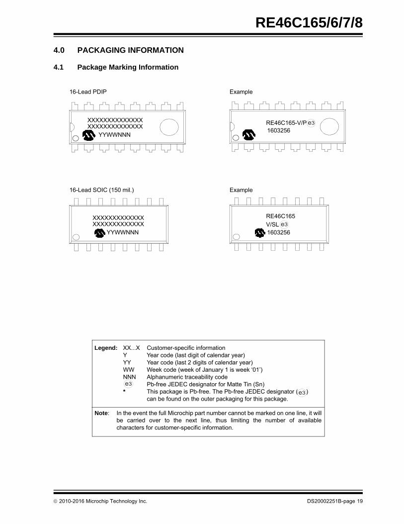
4.0 PACKAGING INFORMATION
4.1 Package Marking Information
16-Lead PDIP Example
Legend: XX...X Customer-specific informationY Year code (last digit of calendar year)YY Year code (last 2 digits of calendar year)WW Week code (week of January 1 is week ‘01’)NNN Alphanumeric traceability code Pb-free JEDEC designator for Matte Tin (Sn)* This package is Pb-free. The Pb-free JEDEC designator ( )
can be found on the outer packaging for this package.
Note: In the event the full Microchip part number cannot be marked on one line, it willbe carried over to the next line, thus limiting the number of availablecharacters for customer-specific information.
3e
3e
1603256RE46C165-V/P^^
16-Lead SOIC (150 mil.) Example
1603256
RE46C165
3e
3e
XXXXXXXXXXXXXXXXXXXXXXXXXXXX
YYWWNNN
XXXXXXXXXXXXXXXXXXXXXXXXXX
YYWWNNNV/SL
2010-2016 Microchip Technology Inc. DS20002251B-page 19

RE46C165/6/7/8
���������� ������������������������������
�� �� �� �������� !�����"�#�$��%!��&������'�(!%�&! %�(�����%�"�)�%����%�����%���"������� *������$����%�+����%�� %���,� ��&�� �� �����"�-��"��%�����!"��&�"�$�� ����%! �� ����"�$�� ����%! �� � ������%��#���"�����.���� �"���� ��&�� ��������"�%���������������-�/���0��
1�+2 1� �����&�� ���� ���%��������#��%����!�� �)��)�%�!%�%������ �
�� � 3�%���& %��!��%����4����"�)��� '����� �� ���%��������������4�����������$���%������%�"��%��%%�255)))�&��������&5���4�����
6��% �7+8-���&�� ���9�&�% ��7 7:� ��;
7!&(��$���� 7 �<��%�� � �����1�+ ��%����%��������� � = = ������"�"����4���� ���4�� �� ���0 ��,� ���01� ��%����%��������� �� ���0 = =��!�"��%���!�"��>�"%� - ���� �,�� �,�0��"�"����4����>�"%� -� ���� ��0� ��?�:������9���%� � ��,0 ��00 ���0 ���%����%��������� 9 ���0 ��,� ��0�9��"� ���4�� � ���? ���� ���06����9��"�>�"%� (� ���0 ��<� ����9)��9��"�>�"%� ( ���� ���? ����:�������)����������* �1 = = ��,�
N
E1NOTE 1
D
1 2 3
A
A1b1
b e
L
A2
E
eB
c
������� ������� ��)��� +������1
DS20002251B-page 20 2010-2016 Microchip Technology Inc.

RE46C165/6/7/8
Note: For the most current package drawings, please see the Microchip Packaging Specification located at
http://www.microchip.com/packaging
2010-2016 Microchip Technology Inc. DS20002251B-page 21

RE46C165/6/7/8
Note: For the most current package drawings, please see the Microchip Packaging Specification located at
http://www.microchip.com/packaging
DS20002251B-page 22 2010-2016 Microchip Technology Inc.

RE46C165/6/7/8
Note: For the most current package drawings, please see the Microchip Packaging Specification located at
http://www.microchip.com/packaging
2010-2016 Microchip Technology Inc. DS20002251B-page 23

RE46C165/6/7/8
NOTES:
DS20002251B-page 24 2010-2016 Microchip Technology Inc.

RE46C165/6/7/8
APPENDIX A: REVISION HISTORY
Revision B (March 2016)
• Removed the 16-Lead SOIC (300 mil.) package reference from Temperature Characteristics table, from Section 4.1 “Package Marking Information” and from the Product Identification System section.
• Updated Package Drawings for 16-Lead SOIC (150 mil.) package in Section 4.0 “Packaging Information”.
Revision A (May 2010)
• Original release of this document.
2010-2016 Microchip Technology Inc. DS20002251B-page 25

RE46C165/6/7/8
NOTES:
DS20002251B-page 26 2010-2016 Microchip Technology Inc.

RE46C165/6/7/8
PRODUCT IDENTIFICATION SYSTEM
To order or obtain information, e.g., on pricing or delivery, refer to the factory or the listed sales office.
PART NO. /X
PackageDevice
Device: RE46C165: CMOS Photoelectric Smoke Detector ASICRE46C165T: CMOS Photoelectric Smoke Detector ASIC
(Tape and Reel, SOIC only)RE46C165/7: CMOS Photoelectric Smoke Detector ASICRE46C165/7T: CMOS Photoelectric Smoke Detector ASIC
(Tape and Reel, SOIC only)RE46C166/8: CMOS Photoelectric Smoke Detector ASICRE46C166/8T: CMOS Photoelectric Smoke Detector ASIC
(Tape and Reel, SOIC only)RE46C165/6: CMOS Photoelectric Smoke Detector ASICRE46C165/6T: CMOS Photoelectric Smoke Detector ASIC
(Tape and Reel, SOIC only)
Tape and Reel Option:
T = Tape and Reel(1)
Package: ES
= Plastic Dual In-Line, 300 mil. Body, 16-Lead (PDIP)= Small Plastic Outline – Narrow, 3.90 mm Body,
16-Lead (SOIC)
Examples:
a) RE46C165E16F: 16LD PDIP Package, Lead-Free
b) RE46C165S16F: 16LD SOIC Package, Lead-Free
c) RE46C165S16TF: 16LD SOIC Package, Tape and Reel, Lead-Free
a) RE46C166E16F: 16LD PDIP Package, Lead-Free
b) RE46C166S16F: 16LD SOIC Package, Lead-Free
c) RE46C166S16TF: 16LD SOIC Package, Tape and Reel, Lead-Free
a) RE46C167E16F: 16LD PDIP Package, Lead-Free
b) RE46C167S16F: 16LD SOIC Package, Lead-Free
c) RE46C167S16TF: 16LD SOIC Package, Tape and Reel, Lead-Free
a) RE46C168E16F: 16LD PDIP Package, Lead-Free
b) RE46C168S16F: 16LD SOIC Package, Lead-Free
c) RE46C168S16TF: 16LD SOIC Package, Tape and Reel, Lead-Free
Note 1: Tape and Reel identifier only appears in the catalog part number description. This identi-fier is used for ordering purposes and is not printed on the device package. Check with your Microchip Sales Office for package availability with the Tape and Reel option.
XX
Numberof Pins
X(1)
Tapeand Reel
X
Lead Free
2010-2016 Microchip Technology Inc. DS20002251B-page 27

RE46C165/6/7/8
NOTES:
DS20002251B-page 28 2010-2016 Microchip Technology Inc.

Note the following details of the code protection feature on Microchip devices:
• Microchip products meet the specification contained in their particular Microchip Data Sheet.
• Microchip believes that its family of products is one of the most secure families of its kind on the market today, when used in the intended manner and under normal conditions.
• There are dishonest and possibly illegal methods used to breach the code protection feature. All of these methods, to our knowledge, require using the Microchip products in a manner outside the operating specifications contained in Microchip’s Data Sheets. Most likely, the person doing so is engaged in theft of intellectual property.
• Microchip is willing to work with the customer who is concerned about the integrity of their code.
• Neither Microchip nor any other semiconductor manufacturer can guarantee the security of their code. Code protection does not mean that we are guaranteeing the product as “unbreakable.”
Code protection is constantly evolving. We at Microchip are committed to continuously improving the code protection features of ourproducts. Attempts to break Microchip’s code protection feature may be a violation of the Digital Millennium Copyright Act. If such actsallow unauthorized access to your software or other copyrighted work, you may have a right to sue for relief under that Act.
Information contained in this publication regarding deviceapplications and the like is provided only for your convenienceand may be superseded by updates. It is your responsibility toensure that your application meets with your specifications.MICROCHIP MAKES NO REPRESENTATIONS ORWARRANTIES OF ANY KIND WHETHER EXPRESS ORIMPLIED, WRITTEN OR ORAL, STATUTORY OROTHERWISE, RELATED TO THE INFORMATION,INCLUDING BUT NOT LIMITED TO ITS CONDITION,QUALITY, PERFORMANCE, MERCHANTABILITY ORFITNESS FOR PURPOSE. Microchip disclaims all liabilityarising from this information and its use. Use of Microchipdevices in life support and/or safety applications is entirely atthe buyer’s risk, and the buyer agrees to defend, indemnify andhold harmless Microchip from any and all damages, claims,suits, or expenses resulting from such use. No licenses areconveyed, implicitly or otherwise, under any Microchipintellectual property rights unless otherwise stated.
2010-2016 Microchip Technology Inc.
Microchip received ISO/TS-16949:2009 certification for its worldwide headquarters, design and wafer fabrication facilities in Chandler and Tempe, Arizona; Gresham, Oregon and design centers in California and India. The Company’s quality system processes and procedures are for its PIC® MCUs and dsPIC® DSCs, KEELOQ® code hopping devices, Serial EEPROMs, microperipherals, nonvolatile memory and analog products. In addition, Microchip’s quality system for the design and manufacture of development systems is ISO 9001:2000 certified.
QUALITY MANAGEMENT SYSTEM CERTIFIED BY DNV
== ISO/TS 16949 ==
Trademarks
The Microchip name and logo, the Microchip logo, AnyRate, dsPIC, FlashFlex, flexPWR, Heldo, JukeBlox, KeeLoq, KeeLoq logo, Kleer, LANCheck, LINK MD, MediaLB, MOST, MOST logo, MPLAB, OptoLyzer, PIC, PICSTART, PIC32 logo, RightTouch, SpyNIC, SST, SST Logo, SuperFlash and UNI/O are registered trademarks of Microchip Technology Incorporated in the U.S.A. and other countries.
ClockWorks, The Embedded Control Solutions Company, ETHERSYNCH, Hyper Speed Control, HyperLight Load, IntelliMOS, mTouch, Precision Edge, and QUIET-WIRE are registered trademarks of Microchip Technology Incorporated in the U.S.A.
Analog-for-the-Digital Age, Any Capacitor, AnyIn, AnyOut, BodyCom, chipKIT, chipKIT logo, CodeGuard, dsPICDEM, dsPICDEM.net, Dynamic Average Matching, DAM, ECAN, EtherGREEN, In-Circuit Serial Programming, ICSP, Inter-Chip Connectivity, JitterBlocker, KleerNet, KleerNet logo, MiWi, motorBench, MPASM, MPF, MPLAB Certified logo, MPLIB, MPLINK, MultiTRAK, NetDetach, Omniscient Code Generation, PICDEM, PICDEM.net, PICkit, PICtail, PureSilicon, RightTouch logo, REAL ICE, Ripple Blocker, Serial Quad I/O, SQI, SuperSwitcher, SuperSwitcher II, Total Endurance, TSHARC, USBCheck, VariSense, ViewSpan, WiperLock, Wireless DNA, and ZENA are trademarks of Microchip Technology Incorporated in the U.S.A. and other countries.
SQTP is a service mark of Microchip Technology Incorporated in the U.S.A.
Silicon Storage Technology is a registered trademark of Microchip Technology Inc. in other countries.
GestIC is a registered trademarks of Microchip Technology Germany II GmbH & Co. KG, a subsidiary of Microchip Technology Inc., in other countries.
All other trademarks mentioned herein are property of their respective companies.
© 2010-2016, Microchip Technology Incorporated, Printed in the U.S.A., All Rights Reserved.
ISBN: 978-1-5224-0434-7
DS20002251B-page 29

DS20002251B-page 30 2010-2016 Microchip Technology Inc.
AMERICASCorporate Office2355 West Chandler Blvd.Chandler, AZ 85224-6199Tel: 480-792-7200 Fax: 480-792-7277Technical Support: http://www.microchip.com/supportWeb Address: www.microchip.com
AtlantaDuluth, GA Tel: 678-957-9614 Fax: 678-957-1455
Austin, TXTel: 512-257-3370
BostonWestborough, MA Tel: 774-760-0087 Fax: 774-760-0088
ChicagoItasca, IL Tel: 630-285-0071 Fax: 630-285-0075
ClevelandIndependence, OH Tel: 216-447-0464 Fax: 216-447-0643
DallasAddison, TX Tel: 972-818-7423 Fax: 972-818-2924
DetroitNovi, MI Tel: 248-848-4000
Houston, TX Tel: 281-894-5983
IndianapolisNoblesville, IN Tel: 317-773-8323Fax: 317-773-5453
Los AngelesMission Viejo, CA Tel: 949-462-9523 Fax: 949-462-9608
New York, NY Tel: 631-435-6000
San Jose, CA Tel: 408-735-9110
Canada - TorontoTel: 905-673-0699 Fax: 905-673-6509
ASIA/PACIFICAsia Pacific OfficeSuites 3707-14, 37th FloorTower 6, The GatewayHarbour City, Kowloon
Hong KongTel: 852-2943-5100Fax: 852-2401-3431
Australia - SydneyTel: 61-2-9868-6733Fax: 61-2-9868-6755
China - BeijingTel: 86-10-8569-7000 Fax: 86-10-8528-2104
China - ChengduTel: 86-28-8665-5511Fax: 86-28-8665-7889
China - ChongqingTel: 86-23-8980-9588Fax: 86-23-8980-9500
China - DongguanTel: 86-769-8702-9880
China - HangzhouTel: 86-571-8792-8115 Fax: 86-571-8792-8116
China - Hong Kong SARTel: 852-2943-5100 Fax: 852-2401-3431
China - NanjingTel: 86-25-8473-2460Fax: 86-25-8473-2470
China - QingdaoTel: 86-532-8502-7355Fax: 86-532-8502-7205
China - ShanghaiTel: 86-21-5407-5533 Fax: 86-21-5407-5066
China - ShenyangTel: 86-24-2334-2829Fax: 86-24-2334-2393
China - ShenzhenTel: 86-755-8864-2200 Fax: 86-755-8203-1760
China - WuhanTel: 86-27-5980-5300Fax: 86-27-5980-5118
China - XianTel: 86-29-8833-7252Fax: 86-29-8833-7256
ASIA/PACIFICChina - XiamenTel: 86-592-2388138 Fax: 86-592-2388130
China - ZhuhaiTel: 86-756-3210040 Fax: 86-756-3210049
India - BangaloreTel: 91-80-3090-4444 Fax: 91-80-3090-4123
India - New DelhiTel: 91-11-4160-8631Fax: 91-11-4160-8632
India - PuneTel: 91-20-3019-1500
Japan - OsakaTel: 81-6-6152-7160 Fax: 81-6-6152-9310
Japan - TokyoTel: 81-3-6880- 3770 Fax: 81-3-6880-3771
Korea - DaeguTel: 82-53-744-4301Fax: 82-53-744-4302
Korea - SeoulTel: 82-2-554-7200Fax: 82-2-558-5932 or 82-2-558-5934
Malaysia - Kuala LumpurTel: 60-3-6201-9857Fax: 60-3-6201-9859
Malaysia - PenangTel: 60-4-227-8870Fax: 60-4-227-4068
Philippines - ManilaTel: 63-2-634-9065Fax: 63-2-634-9069
SingaporeTel: 65-6334-8870Fax: 65-6334-8850
Taiwan - Hsin ChuTel: 886-3-5778-366Fax: 886-3-5770-955
Taiwan - KaohsiungTel: 886-7-213-7828
Taiwan - TaipeiTel: 886-2-2508-8600 Fax: 886-2-2508-0102
Thailand - BangkokTel: 66-2-694-1351Fax: 66-2-694-1350
EUROPEAustria - WelsTel: 43-7242-2244-39Fax: 43-7242-2244-393
Denmark - CopenhagenTel: 45-4450-2828 Fax: 45-4485-2829
France - ParisTel: 33-1-69-53-63-20 Fax: 33-1-69-30-90-79
Germany - DusseldorfTel: 49-2129-3766400
Germany - KarlsruheTel: 49-721-625370
Germany - MunichTel: 49-89-627-144-0 Fax: 49-89-627-144-44
Italy - Milan Tel: 39-0331-742611 Fax: 39-0331-466781
Italy - VeniceTel: 39-049-7625286
Netherlands - DrunenTel: 31-416-690399 Fax: 31-416-690340
Poland - WarsawTel: 48-22-3325737
Spain - MadridTel: 34-91-708-08-90Fax: 34-91-708-08-91
Sweden - StockholmTel: 46-8-5090-4654
UK - WokinghamTel: 44-118-921-5800Fax: 44-118-921-5820
Worldwide Sales and Service
07/14/15


![Car Alarms & Smoke Alarms [Monitorama]](https://static.fdocuments.net/doc/165x107/54b6cdf94a7959d84d8b45a5/car-alarms-smoke-alarms-monitorama.jpg)