RD6 Progress January 2015 TK Hemmick for RD6. RD6 Core Program Summary Stony Brook University (SBU):...
40
RD6 Progress January 2015 TK Hemmick for RD6
-
Upload
eileen-heath -
Category
Documents
-
view
220 -
download
0
Transcript of RD6 Progress January 2015 TK Hemmick for RD6. RD6 Core Program Summary Stony Brook University (SBU):...

RD6 Progress January 2015
TK Hemmick for RD6

RD6 Core Program Summary• Stony Brook University (SBU):
• CF4-based RICH for hadron ID at high momentum (EIC also needs low-p hadron-ID).
• UV Focal Plane for TPC/HBD hybrid detector.
• Brookhaven National Laboratory (BNL):
• Mini-drift enhancement of planar trackers to improve resolution for inclined tracks.
• Drift section for TPC/HBD (TPC=BNL, photocathodes from SBU).
• Yale University
• 3-coordinate pad/strip readout technology.
• Gas studies for TPC.
• Hybrid avalanche studies to reduce IBF in TPC designs.
• Florida Institute of Technology (FIT):
• Full-scale forward EIC tracking detector using zigzag strips (lowest channel count)
• University of Virginia (UVa):
• Full scale LOW MASS forward tracker w/ “Stereo Compass” (highest resolution)
• JOINT EFFORT (FIT, UVa, Temple University)
• Develop common large GEM design to reduce overall costs of these efforts.

Integrated Strategy Leading to EIC.• RD6 has earned a good reputation for spending EIC R&D funds
wisely and producing many publishable results (more will be shown today).
• Until now the work can mostly be described as “generic R&D”.
• Rumors of good news coming from the Long Range Planning process, require that we make our plans with a clear and flexible vision.
• Rumors of bad news for available funds in the coming fiscal year require that our plans allow for continuity of the effort despite limited funding.
• Our plans include a strategy to ensure consortium health & flexibility:
• We propose to distribute funding of the forward tracking effort over 4 years.
• We propose to complete continuing generic work as additional funds allow.
• Our priorities are:
• Continued support for postdoc who is principle player in common GEM design.
• Funding of AT LEAST the first year of our new 4-year timeline.
• TPC R&D including hybrid gain studies and TPC-HBD prototype.
• RICH R&D including large scale mirrors & charge sharing technology.
3

4 Year Forward Tracking Plan
Year Item Per Institution
Total RD6 Subtotal
2015 NRE-1 $33k $99k $66k
2016 NRE-2 & Foils $64.5k $193.5k $129k
2017 First Article Chamber(s)
$26k $78k $52k
2018 Production (2x3=6) $40k $120k $80k
TOTAL $163.5k $490.5k $327k
• Our plan implements the requested enthusiastic continuation in lean times..
• The end result is a set of 3-each full sized chambers with differing design paradigms allowing for technology selection.
• This funding profile fits nicely with the collaboration formation process and allow adaption to eventual designs (lemonade from lemons…)
• This profile will allow the effort to smoothly move from generic to specific.
• Domestic production will be a boon to the entire field.
4
“The common work of UVa and FIT with B. Surrow of eRD3 is an excellent development and should be continued enthusiastically.”
--EIC R&D Committee Report, January 2015
Generic R&D
Directed R&D

C.Woody, EIC R&D Committee Meeting, 7/9/15 5
Final Results on Minidrift GEM DetectorPosition Resolution Angular Resolution
• Chevrons : 2x10 mm2 pads containing interleaving zigzag electrodes with a 0.5 mm pitch
• Strips: COMPASS style XY strips (80 mm top and 350 mm bottom) each with a 400 mm pitch
• Time Slice Method uses centroid found in each time bin and central time value of each time bin to fit a vector in the drift gap
• Final results are being written up and submitted for publication in the IEEE Transactions on Nuclear Science

C.Woody, EIC R&D Committee Meeting, 7/9/15 6
The Actual Detector
• Three sided field cage allows for installation of a fourth foil side or a wire frame that allows passage of Cherenkov light to the photosensitive GEM detector
• Photosensitive GEM is mounted on a
movable stage to allow varying its position relative to the TPC detector
Laser port
HV connection
Transparent Window

C.Woody, EIC R&D Committee Meeting, 7/9/15 7
Field Distortions with One Plane of Wires for Field Cage
4 sides of strips 3 sides of strips + 1 side of wires
Slice in XY plane at mid ZWire plane is at X=0
M.Phipps
C.Woody, EIC R&D Committee Meeting, 7/9/15 8
First Tests of the TPC GEM
Fe-55
Scan across chevron pads with collimated X-ray source
Position Resolution
Uncorrected: 132 mmCorrected: 98 mm
Reconstructed track with GEMs configured as a Minidrift Detector

C.Woody, EIC R&D Committee Meeting, 7/9/15 9
Future Plans
Final results on studies done with Minidrift GEM detector will be submitted for publication in IEEE TNS within the next few weeks.
Testing will continue on the TPC/Cherenkov prototype detector, focusing mainly on the TPC portion. • Study various drift gases (Ar/CO2, CF4, CF4 and Ne mixtures)• Measure drift velocities, resolutions, charge attachment, ion
backflow, etc• Reconstruct cosmic ray tracks over full drift region• Study HV effects of moving photosensitive GEM close to field cage
Make CsI photocathodes and measure QE (with the help of Stony Brook)
Install CsI photosensitive GEM in detector and study combined detector in the lab with radioactive sources and cosmic rays
Test the detector in the beam at Fermilab in 2016
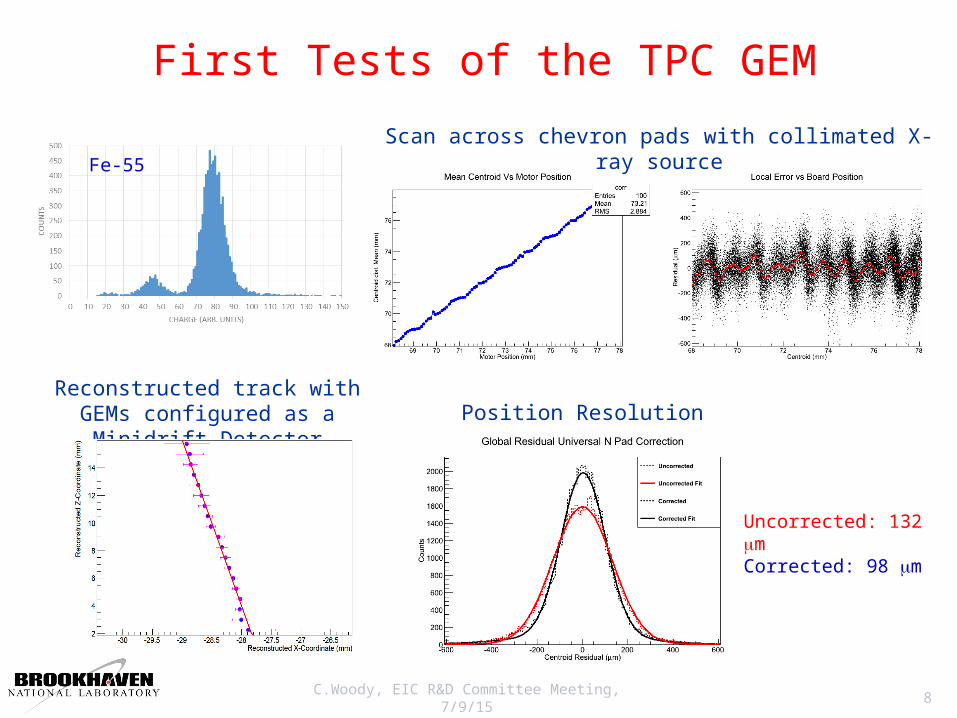
Impact of Multiple Coulomb Scattering on Tracking in the 2013 FNAL Beam Test with a Stand-alone Geant4 Simulation
Hit positions(25 GeV/c pions)
Overall scattering angle distributions between REF1 tracker detector and the other three tracker detectors (25 GeV/c pions)
GEANT4 geometryfor FNAL beam test
Zigzag readout strips
10

Final Results on Angular Resolution for the large-area GEM with Zigzag Strip Readout
Measured Tracker resolutions are 73 µm, 70 µm, 59 µm, and 68 µm for REF1-4, respectively.
For the GEM with zigzag-strip readout, the measured angular resolution is 193 urad at the highest tested voltage. Here track errors are estimated from the Geant4 simulation taking multiple scattering fully into account in this final result. All strip-multiplicity are used for strip clusters in this result; centroid positions of clusters with 2 and 3 strips are corrected for non-linear strip response (blue points). 11

Comparison of Resolutions Obtained with Track-error Method with Geometric-Mean Method via Geant4 Simulation
On the left plot, all trackers are assumed to have 50 µm resolution; on the right plot, tracker resolutions that are put into the simulation are the actual resolutions from the experimental data.We observe that the geometric-mean method underestimates the resolutions by ~10% while the track-error method produces very accurate results. Multiple scattering is fully considered in this simulation.
Resolution comparison for the zigzag GEM in polar coordinates from beam test data. Geometric mean method underestimates the angular resolution by 7-11% .
12

EIC forward tracker prototype – Common GEM foil design
Overview:
• 30.1° opening angle for single prototype to allow for overlap of adjacent chambers.
• Active foil length is ~90 cm.• The foil is segmented into 24 sectors. 8 sectors at
the lower eta region are segmented mainly in the R direction; 16 sectors at the higher eta region are in the ϕ direction.
• This common GEM foil design will be used by the forward tracker task force (the groups from Temple U., U. Va, and Florida Tech).
• Funds are requested for commercial production of these foils by Tech-Etch Inc. in 2016 and 2017. 13

EIC forward tracker prototype – Common GEM foil design
• There are HV pads (red) outside of a closed chamber for the Temple U and U. Va design approaches. The HV traces (red) are brought individually to each foil sector.
• The HV pads for the Florida Tech group are integrated into stretching frames; they connect to foil sectors through protective resistors that are mounted directly on the foils.
• To avoid crossings between FIT HV traces and the other HV traces, we put common HV lines on the bottom surface of the foil, and we use other pads (2mm size) with hole arrays to create vias to connect the two sides. These hole arrays will be filled up with conductive glue to make the connection.
Design Detail of HV paths:
14

EIC GEM R&D @ UVa: What was done
• Design of common GEM foil (UVa, FIT and TU groups ) for EIC-FT-GEM-II prototype
• Bi-weekly working group meeting (discussion included people from Yale and Tech Etch Company)
• Common GEM foil accommodates requirements by different assembly techniques from the 3 groups
• Actual drawing and finalization of the design by A. Zhang (see FIT slides)
• 2D stereo angle flexible readout board for EIC-FT-GEM-II
• New ideas to be tested for all FEC cards on the outer radius side of the chamber
• Discussion and preliminary drawings held with expert at CERN
• Ongoing R&D at UVa that are of particular interest for EIC-FT-GEM-II prototype.
• New assembly technique being proposed and tested at UVa
• Test of light GEM with Cr-GEM foil.
• Preparation for publication of the FTBF test beam results in a peer review journal
• Analysis of the FTBF test beam data now completed
• Finalizing the manuscript for submission to TNS (or NIM A) peer review journal the July 2015
EIC Tracking R&D @ Univ. of Virginia

EIC GEM R&D @ UVa: New assembly technique
• New construction: hybrid between CMS GEM
NS2 technique and assembly technique where all
frames are glued together.
• GEM glued onto frames but framed GEMs are
stacked with O-ring and screws (not glued).
• Pros: re-open the chamber to replace parts
• Cons: Lots of screws, compromise between
strength and material budget of the screws.
Entrance window
Drift region
Transfer region I
Transfer region II
Induction region
spacers
2D readout board
O-ring
Idea was first tested on the (120 55 cm2 ) Triple-GEM chamber for Hall B pRad Experiment
Exploded 3D view
Cross sectional view
EIC Tracking R&D @ Univ. of Virginia
Plastic screws holding the frames
together and closing the chamber

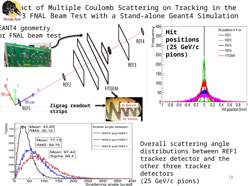
EIC GEM R&D @ UVa: Light GEM detector Mass Cr-GEM foilCr-GEM foil
• Copper (Cu) clad Kapton material comes with 100 nm
Chromium (Cr) layer between Cu and Kapton
• 5 m Cu layers removed from top and bottom and leave
only 100 nm Cr layers as metallic electrodes
• Cr-GEM foils from CERN PCB workshop
5 m Cu
50 m Kapton
Standard GEM
100 nm Cr50 m Kapton
Cr-GEM
100 nm Cr
2D hit map on Cr-Triple-GEM with CosmicsEIC Tracking R&D @ Univ. of Virginia
EIC GEM R&D @ UVa: Light GEM detector with Cr-GEM foil
Quantity Thickness Density X0 Area X0 S-Densitymm g/cm3 mm Fraction % g/cm2
WindowKapton 2 25 1.42 286 1 0.0175 0.0071
DriftCopper 1 5 8.96 14.3 1 0.0350 0.0045Kapton 1 50 1.42 286 1 0.0175 0.0071
GEM FoilCopper 6 5 8.96 14.3 0.8 0.1678 0.0215Kapton 3 50 1.42 286 0.8 0.0420 0.0170
Grid SpacerG10 3 2000 1.7 194 0.008 0.0247 0.0082
ReadoutCopper-80 1 5 8.96 14.3 0.2 0.0070 0.0009
Copper-350 1 5 8.96 14.3 0.75 0.0262 0.0034Kapton 1 50 1.42 286 0.2 0.0035 0.0014Kapton 1 50 1.42 286 1 0.0175 0.0071
NoFlu glue 1 60 1.5 200 1 0.0300 0.0090Gas
(CO2) 1 15000 1.84E-03 18310 1 0.0819 0.0028Total 0.471 0.090
Quantity Thickness Density X0 Area X0 S-Densitymm g/cm3 mm Fraction % g/cm2
WindowKapton 2 25 1.42 286 1 0.0175 0.0071
DriftCopper 1 0 8.96 14.3 1 0.0000 0.0000Kapton 1 50 1.42 286 1 0.0175 0.0071
GEM FoilCopper 6 0 8.96 14.3 0.8 0.0000 0.0000Kapton 3 50 1.42 286 0.8 0.0420 0.0170
Grid SpacerG10 3 2000 1.7 194 0.008 0.0247 0.0082
ReadoutCopper-80 1 0 8.96 14.3 0.2 0.0000 0.0000
Copper-350 1 0 8.96 14.3 0.75 0.0000 0.0000Kapton 1 50 1.42 286 0.2 0.0035 0.0014Kapton 1 50 1.42 286 1 0.0175 0.0071
NoFlu glue 1 60 1.5 200 1 0.0300 0.0090Gas
(CO2) 1 15000 1.84E-03 18310 1 0.0819 0.0028Total 0.235 0.060
Triple-GEM with standard GEM foil Triple-GEM with Cr-GEM foil
About 50% reduction in the amount of material in a EIC-FT-GEM with Cr-GEM
Main motivation:
• Reduce background in high rate photon environment
• Reduce Multiple Scattering
EIC Tracking R&D @ Univ. of Virginia

EIC GEM R&D @ UVa: What’s next
• Common GEM foil for EIC-FT-GEM-II prototype
• Pursue the collaboration with Florida Tech and Temple Univ. on the common GEM foil
• Production of first batch of common GEM Foil by Tech Etch is the highest priority
• R&D at UVa for EIC-FT-GEM-II prototype.
• Design of the readout board to be completed later this year (October 2015)
• New assembly technique: Investigate low mass and high strength material (Carbon fiber, PEEK …)
for the screws and nuts
• Continue the study of Cr-GEM: gain curve, discharge probability and high rate performance etc .. .
• Publication on the FTBF test beam results in a peer review journal
• End of July 2015 for first submission
EIC Tracking R&D @ Univ. of Virginia

IBF and Energy Resolution Measurements for 2-GEM + MMG Structures.
Develop techniques and technology to build TPC’s with good resolution (space, energy loss) and low dead time.
• Choice of gas• Design of gain structure• Minimize cost
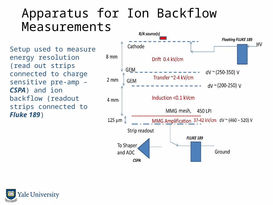
Setup used to measure energy resolution (read out strips connected to charge sensitive pre-amp – CSPA) and ion backflow (readout strips connected to Fluke 189)
Apparatus for Ion Backflow Measurements

Energy resolution for 55Fe X-ray vs. Ion Backflow for various gas mixes.
Each curve is for one gas mix
The points along a curve are for different MMG voltages, varying the GEM voltages to keep the overall gain ~2000
Ion Backflow Results
Best result of any avalanche technology measured to date.

• Multilayer Grid stacked in TPC drift direction (Howard Wieman*)• Alternative way to deal with IBF and keep low dead time
• hundreds of msec for ions from gain structure to drift through structure when it is biased to be transparent for electrons and ions
• tens of msec to collect ions when structure is biased to clear ions
Plots are simulation of Ion clearing time for a stacked grid structure in a TPCANSYS and Garfield++ , Clearing field is parallel to TPC drift fieldLong tail is from Ions initially in low field region between grid wires
Simulation of Ion clearing time for a stacked grid structure in a TPC*
* http://www-rnc.lbl.gov/~wieman/alice%20upgrade%20gating%20grid.pdf

Hybrid Gain Stage Continuing Research Plans:• Investigate ways to minimize discharges in MMG
resistive layer further measurements on floating strip circuit
• Study stacked grid structures to minimize ion backflow Build small prototype to explore different configurations Study different clearing field time profiles – move low field
region during clearing cycle

• Publication resubmitted following reviewer comments.
• Currently awaiting results.
• Superb performance, but can do better!• Limitation is position resolution.• Charge cloud too small for geometrical
charge division (s ~ 150 mm)
• Two options:• decrease pad size ($$)• increase signal spread – R&D
RICH Prototype Resolution is Segmentation Limited
p/K Performance Extrapolation
Current Device: 2.4s @ 50 GeV/cImprovement: 2.5s @ 60 GeV/c
NOTE: EIC wiki states 50 GeV/c as desired /p K goal.
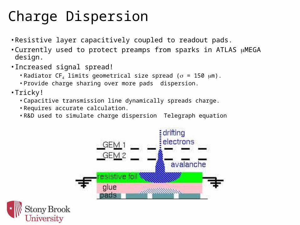
• Resistive layer capacitively coupled to readout pads.• Currently used to protect preamps from sparks in ATLAS mMEGA design.• Increased signal spread!
• Radiator CF4 limits geometrical size spread (s = 150 mm).• Provide charge sharing over more pads dispersion.
• Tricky! • Capacitive transmission line dynamically spreads charge.• Requires accurate calculation.• R&D used to simulate charge dispersion Telegraph equation
Charge Dispersion
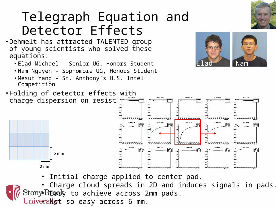
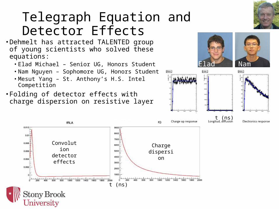
Telegraph Equation and Detector Effects
• Dehmelt has attracted TALENTED group of young scientists who solved these equations:
• Elad Michael – Senior UG, Honors Student• Nam Nguyen – Sophomore UG, Honors Student• Mesut Yang – St. Anthony’s H.S. Intel Competition
• Folding of detector effects with charge dispersion on resistive layer
Elad Nam
• Initial charge applied to center pad.• Charge cloud spreads in 2D and induces signals in pads.• Easy to achieve across 2mm pads.• Not so easy across 6 mm.

Pad Response Function
• Charge fraction on “central pad” vs charge center position.• When segmented at 2 mm, the resistive charge division will work. • When segmented at 9 mm, it will not.
PRF calculation for 2x6 mm2 pads for different pads compared to previous results (green curve).
PRF calculation for 9x9 mm2 pads
not feasible
NOTE: Due to a plotting error, please don’t compare results to green curve.
Yes No
Implications and Next steps.
• The RICH detector is an anomalous case of position resolution:• Improved position resolution will improve device performance only when it is the
limiting factor: s=500mm is the “cross-over”.
• Catch 22:• For 2mm pads, resistive charge division is way better than .• For larger sized pads, resistive charge division helps little.• Trackers would benefit from resistive charge division (e.g. hybrid gain stage)• The RICH would not benefit since 2 mm pixels are already near the diffusion limit.
• To continue with a tracking-driven interest we would:• Optimize charge dispersion calculations• Apply resistive layer on simple pad plane.• Verify performance with x-ray gun.

Budget Summary (coming year only)
• Plans include ambitious 4-year development.• Tables apply only to the immediate funding period.• Tables here INCLUDE funds to Temple for common effort.
Full
Minimal
Top Priority:• Postdoc @ FITSecond Priority:• Joint effortThird Priority• Continuing TPCFourth Priority• Continuing RICH

BACKUPS

C.Woody, EIC R&D Committee Meeting, 7/9/15 32
BNL Progress since last meeting
1. What was planned for this period ? Complete the analysis of the test beam data from the Minidrift Detector
Finish construction of the TPC/Cherenkov prototype detector
2. What was accomplished ? The analysis of the test beam data is essentially complete. The final results
have been written up in a paper that is about to be submitted to the IEEE Transactions on Nuclear Science. The draft is in the final stages of preparing the figures and will be submitted with the next few weeks.
The construction of the TPC/Cherenkov prototype is now complete with the exception of the installation of the photosensitive CsI GEM. This will be done after initial testing of the TPC portion of the detector.

C.Woody, EIC R&D Committee Meeting, 7/9/15 33
3 Sided Field Cage + 1 Sided Foil
Kapton foil with 3.9 mm copper strips with 0.1 mm gapsTested to full operating voltage of 1 kV/cm

EIC forward tracker prototype – Common GEM foil design
Overall Technical Design is finished:
34

C.Woody, EIC R&D Committee Meeting, 7/9/15 35
Field Distortions with Addition of Cherenkov Mesh
M.Phipps
No Cherenkov mesh Cherenkov mesh at -15 mm
Cherenkov mesh at -25 mm Cherenkov mesh at -40 mm

C.Woody, EIC R&D Committee Meeting, 7/9/15 36
Electrostatic SimulationTop Plate
Wire Plane
Mirrored Strip Plane
Cherenkov Mesh
Z
X
Y
ANSYS
M.Phipps

C.Woody, EIC R&D Committee Meeting, 7/9/15 37
TPC GEM Detector with Chevron readout board
10x10 cm2 Triple GEM 2 x10 mm Chevron Strips0.5 mmm pitch

38
TPC/Cherenkov Detector
C.Woody, EIC R&D Committee Meeting, 7/9/15
3 SidedField Cage Foil
Field CageWire Plane
Top HV Plate
Movable CsI GEM
Drift
Č
TPC GEM
3D Model
Telegraph Equation and Detector Effects
• Dehmelt has attracted TALENTED group of young scientists who solved these equations:
• Elad Michael – Senior UG, Honors Student• Nam Nguyen – Sophomore UG, Honors Student• Mesut Yang – St. Anthony’s H.S. Intel Competition
• Folding of detector effects with charge dispersion on resistive layer
t (ns)
Charge dispersion
t (ns)
Convolution detector effects
Elad Nam

Detector Response Across Pads
• Calculate distinct pad pattern, e.g., 3 x 5 pads with 2x6mm2 dimensions
• Initial charge applied to center pad.• Charge cloud spreads in 2D and induces signals in pads.• Easy to achieve across 2mm pads.• Not so easy across 6 mm.