
RAE-5 CELLULAR PHONE/ PERSONAL DIGITAL ASSISTANT 9210i.pdf · Nokia requires that phone repair...
404
Technical Documentation Programs After Market Services (PAMS) Copyright E 2002. Nokia Corporation. All Rights Reserved. SERVICE MANUAL [NMP Part No.0275578] RAE-5 CELLULAR PHONE/ PERSONAL DIGITAL ASSISTANT RAE-5 ISSUE 1 04/2002
Transcript of RAE-5 CELLULAR PHONE/ PERSONAL DIGITAL ASSISTANT 9210i.pdf · Nokia requires that phone repair...

Technical Documentation
Programs After Market Services (PAMS)
Copyright 2002. Nokia Corporation. All Rights Reserved.
[NMP Part No.0275578]
RAE-5 CELLULAR PHONE/PERSONAL DIGITAL
ASSISTANT
RAE-5 ISSUE 1 04/2002

RAE-5Foreword PAMS Technical Documentation
Draft 01 04/02Page 2 Nokia Corporation
AMENDMENT RECORD SHEET
AmendmentNumber
Date Inserted By Comments
04/2002 OJuntunen

RAE-5ForewordPAMS Technical Documentation
Draft 01 04/02 Page 3 Nokia Corporation
RAE-5SERIES CELLULAR PHONE
SERVICE MANUAL
CONTENTS:
1. Foreword (this section)
2. General Information
3. RF+ System Module KL8
4. UIF Modules
5. Variants
6. Service Tools
7. Service Software and Tuning Instructions
8. Troubleshooting Instructions
9. Schematic Diagrams
10. Parts List
11. Disassembly and Service Instructions
12. Accessories

RAE-5Foreword PAMS Technical Documentation
Draft 01 04/02Page 4 Nokia Corporation
IMPORTANT
This document is intended for use by qualified service personnel only.
Company Policy
Our policy is of continuous development; details of all technical modifications willbe included with service bulletins.
While every endeavour has been made to ensure the accuracy of this document,some errors may exist. If any errors are found by the reader, NOKIA MOBILEPHONES Ltd should be notified in writing.
Please state:Title of the Document + Issue Number/Date of publication
Latest Amendment Number (if applicable)
Page(s) and/or Figure(s) in error
Please send to: Nokia Mobile Phones LtdPAMS Technical DocumentationPO Box 8624101 SALOFinland

RAE-5ForewordPAMS Technical Documentation
Draft 01 04/02 Page 5 Nokia Corporation
Warnings and CautionsPlease refer to the phone’s user guide for instructions relating to operation,care and maintenance including important safety information. Note also thefollowing:
Warnings:1. CARE MUST BE TAKEN ON INSTALLATION IN VEHICLES
FITTED WITH ELECTRONIC ENGINE MANAGEMENTSYSTEMS AND ANTI–SKID BRAKING SYSTEMS. UNDERCERTAIN FAULT CONDITIONS, EMITTED RF ENERGY CANAFFECT THEIR OPERATION. IF NECESSARY, CONSULT THEVEHICLE DEALER/MANUFACTURER TO DETERMINE THEIMMUNITY OF VEHICLE ELECTRONIC SYSTEMS TO RFENERGY.
2. THE CELLULAR TELEPHONE MUST NOT BE OPERATED INAREAS LIKELY TO CONTAIN POTENTIALLY EXPLOSIVEATMOSPHERES EG PETROL STATIONS (SERVICE STATIONS),BLASTING AREAS ETC.
3. OPERATION OF ANY RADIO TRANSMITTING EQUIPMENT,INCLUDING CELLULAR TELEPHONES, MAY INTERFERE WITHTHE FUNCTIONALITY OF INADEQUATELY PROTECTEDMEDICAL DEVICES. CONSULT A PHYSICIAN OR THEMANUFACTURER OF THE MEDICAL DEVICE IF YOU HAVEANY QUESTIONS. OTHER ELECTRONIC EQUIPMENT MAYALSO BE SUBJECT TO INTERFERENCE.
Cautions:1. Servicing and alignment must be undertaken by qualified
personnel only.
2. Ensure all work is carried out at an anti–static workstation and thatan anti–static wrist strap is worn.
3. Ensure solder, wire, or foreign matter does not enter the telephoneas damage may result.
4. Use only approved components as specified in the parts list.
5. Ensure all components, modules screws and insulators arecorrectly re–fitted after servicing and alignment. Ensure all cablesand wires are repositioned correctly.
6. All PC’s used with NMP Service Software for this produce must bebios and operating system ”Year 2000 Compliant”.

RAE-5Foreword PAMS Technical Documentation
Draft 01 04/02Page 6 Nokia Corporation
ESD Protection
Nokia requires that phone repair places have sufficient ESD protection(against static electricity) when servicing cellular phones.
A cellular phone, which is ready for use, can be handled normally withoutESD protection. The SIM card and battery can be replaced in normalconditions of use.
To replace the color cover ESD protection must be applied, except for thephone covers which can be replaced by the customer.
All electronic parts of the phone , including the display, are susceptible toESD. Resistors, too, can be damaged by static electricity discharge.
All ESD sensitive parts must be packed in metallized protective bags duringshipping and handling outside any ESD Protected Area (EPA).
Every repair action involving opening the phone or handling the phonecomponents must be done under ESD protection.
ESD protected spare part packages MUST NOT be opened/closed out of anEPA.
For more detailed information about ESD protection and EPA, contact yourlocal Nokia After Market Services representative.

PAMS Technical DocumentationRAE-5 Series PDA
Issue 1 04/02 Copyright 2002. Nokia Corporation. All Rights Reserved.
2. General Information

PAMS
Technical Documentation
RAE-5 2. General Information
Page 2 – 2 Issue 1 04/02
AMENDMENT RECORD SHEET
AmendmentNumber
Date Inserted By Comments
04/02 OJuntunen

PAMS
Technical Documentation
RAE-5
2. General Information
Page 2 – 3Issue 1 04/02
CONTENTS –Troubleshooting
Page No
Introduction to RAE–5 2 – 4. . . . . . . . . . . . . . . . . . . . . . . . . . . . . . . . . . .
Technical Summary 2 – 4. . . . . . . . . . . . . . . . . . . . . . . . . . . . . . . . . . . List Of Modules 2 – 6. . . . . . . . . . . . . . . . . . . . . . . . . . . . . . . . . . . .
Accessories 2 – 7. . . . . . . . . . . . . . . . . . . . . . . . . . . . . . . . . . . . . . . . . General Accessories 2 – 7. . . . . . . . . . . . . . . . . . . . . . . . . . . . . . . Portable And Office Accessories 2 – 7. . . . . . . . . . . . . . . . . . . . . Mobile Accessories 2 – 7. . . . . . . . . . . . . . . . . . . . . . . . . . . . . . . . .

PAMS
Technical Documentation
RAE-5 2. General Information
Page 2 – 4 Issue 1 04/02
Introduction to RAE-5
RAE–5 is a dualband communicator with high speed data (HSCSD) for theGSM 900 and DCS1800 networks and keyboards customized for the Chineselanguage. The GSM power class is 4 and the PCN power class is 1.
The RAE-5 Communicator provides an advanced and versatile connection be-tween people via various media: cellular phone, fax, sms, e–mail and internet.
Technical Summary
The communicator has a full graphic phone display and a user interface basedon two soft keys on the front cover.
The device comprises two user interfaces. The conventional cellular phone in-terface is on the front cover. By opening the device the user can access thegraphical user interface to use the Personal Digital Assistant.
Figure 1. RAE-5 CMT Interface
The RAE-5 has a clamshell structure. The PDA display and full QWERTY key-board are visible when the device is opened. The PDA user interface has a fullgraphic 640 x 200 colour ( 4096 colours ) display.
The phone employs a fixed stripline antenna. The bottom ’system’ connectorincorporates a RF connector for car–kit antenna connection.

PAMS
Technical Documentation
RAE-5
2. General Information
Page 2 – 5Issue 1 04/02
Figure 2. RAE-5 PDA Interface
The communicator has a leakage tolerant earpiece and omnidirectional micro-phone providing excellent audio quality. Full rate, enhanced full rate and halfrate speech decoding is supported. High quality personal hands free functional-ity is also provided.
An integrated IrDA link is provided for data transfer between two RAE-5 com-municators or between the communicator and a PC or printer. RS232 connec-tion can also be used between communicator and PC.
A Memory Card slot is located inside the communicator. This card can be usedto extend user data memory and to store applications.
The SIM ( Subscriber Identity Module ) card is located inside the communicator,next to the battery pack..

PAMS
Technical Documentation
RAE-5 2. General Information
Page 2 – 6 Issue 1 04/02
MMC Card
SIM Card
Figure 3. MMC and SIM Cards
The RAE-5 is running both PDA and phone software in a single RISC CPU.The RAE-5 is also using EPOC32 operating system based software platform.(EPOC32 is an operating system from Psion Software Inc.)
NOTE: Due to the infrared data link the RAE-5 is officially specificed as :
CLASS 1 LASER PRODUCT.
See IEC 60825–1 specification 825–1; Labelling, 5.1 General 5.2 Class 1.
List Of Modules
The bottom assembly contains one electronic module. This contains a singlePWB (KL8 ).
Name of module Type code Notes
RF & System Module KL8 Standard KL8 PWB with FLASH memories
Keyboard and hinge flexmodule
UL8 Module built up from FL1 FPC, AF8 audioPWB and connectors
UI Module DL2 PDA & CMT displays built onto UL2 PWB
Mechanics MRAE–3 All mechanical parts excluding language de-pendant parts, like QWERTY–Keymat andsome others.
For variant information kindly refer to the Variants section of this manual.

PAMS
Technical Documentation
RAE-5
2. General Information
Page 2 – 7Issue 1 04/02
Accessories
General Accessories
Batteries:
Name of module Type code Materialcode
Notes
High–power Battery BLL–3 0670290 Lithium–ion 1300 mAh (prismatic cell )
Chargers:
Name of module Type code Materialcode
Notes
Fast Travel Charger ACP–12E 0675294 Euro–plug, operating voltage 90 .. 264Vac
Fast Travel Charger ACP–12X 0675296 UK–plug, operating voltage 90 .. 264Vac
Fast Travel Charger ACP–12C 0675297 Chinese–plug and label. 90 .. 264 Vac
Fast Travel Charger ACP–12A 0675300 Australia–plug, operating voltage 90 ..264 Vac
Mobile Charger LCH–9 0675120 Operating voltage 10.8 .. 32 Vdc
Portable And Office Accessories
Name of module Type code Materialcode
Notes
Headset HDC–8L 0694079
Carry Case CBR–44 0720262
Advanced Desktop Stand DCH–10 0675209
RS232 Adapter Cable DLR–2 0271367 Cable between communicator and PCserial port
Memory Card DTS–64 0273026
Mobile Accessories
Name of module Type code Materialcode
Notes
Advanced Active Car Holder CRM–1 0630220
Mounting Plate MKU–1 0620036
Swivel Mount HHS–13 0620055
Hands Free HFU–2 0694049 Hands free to be used with MCC–x
Handset HSU–1 0640047 Handset to be used with HFU–2
HF Microphone HFM–8 0690016 Microphone to be used with HFU–2
HF Speaker HFS–12 0692008 Speaker to be used with HFU–2
Power cable PCH–4J 0730055 Power cable to be used with HFU–2

PAMS
Technical Documentation
RAE-5 2. General Information
Page 2 – 8 Issue 1 04/02
This page intentionally left blank.

PAMS Technical DocumentationRAE-5 Series PDA
Issue 1 04/02 Copyright 2002. Nokia Corporation. All Rights Reserved.
3. RF+System Module KL8

PAMS
Technical Documentation
RAE-5
3. RF+System Module KL8
Page 3 – 2 Issue 1 04/02
AMENDMENT RECORD SHEET
AmendmentNumber
Date Inserted By Comments
04/02 OJuntunen

PAMS
Technical Documentation
RAE-5
3. RF+System Module KL8
Page 3 – 3Issue 1 04/02
CONTENTS –Troubleshooting
Page NoAbbreviations 3 – 6. . . . . . . . . . . . . . . . . . . . . . . . . . . . . . . . . . . . . . . .
RAE-5 Structure 3 – 9. . . . . . . . . . . . . . . . . . . . . . . . . . . . . . . . . . . . . . . .
RAE-5 Modules 3 – 9. . . . . . . . . . . . . . . . . . . . . . . . . . . . . . . . . . . . . . . . .
List of Modules 3 – 9. . . . . . . . . . . . . . . . . . . . . . . . . . . . . . . . . . . . Technical Summary of System Part 3 – 10. . . . . . . . . . . . . . . . . . . . . Block Diagram 3 – 11. . . . . . . . . . . . . . . . . . . . . . . . . . . . . . . . . . . . . . .
Electrical Characteristics 3 – 12. . . . . . . . . . . . . . . . . . . . . . . . . . . . . . . . .
Power Supply 3 – 12. . . . . . . . . . . . . . . . . . . . . . . . . . . . . . . . . . . . . . . . System Connector 3 – 13. . . . . . . . . . . . . . . . . . . . . . . . . . . . . . . . . . . . Battery Connector 3 – 14. . . . . . . . . . . . . . . . . . . . . . . . . . . . . . . . . . . . Backup battery connector 3 – 15. . . . . . . . . . . . . . . . . . . . . . . . . . . . . . SIM card connector 3 – 15. . . . . . . . . . . . . . . . . . . . . . . . . . . . . . . . . . . MMC Connector 3 – 16. . . . . . . . . . . . . . . . . . . . . . . . . . . . . . . . . . . . . . Infrared interface 3 – 16. . . . . . . . . . . . . . . . . . . . . . . . . . . . . . . . . . . . . UI Signals 3 – 17. . . . . . . . . . . . . . . . . . . . . . . . . . . . . . . . . . . . . . . . . . . System – RF interface 3 – 21. . . . . . . . . . . . . . . . . . . . . . . . . . . . . . . .
Functional Description 3 – 24. . . . . . . . . . . . . . . . . . . . . . . . . . . . . . . . . . .
Modes of Operation 3 – 24. . . . . . . . . . . . . . . . . . . . . . . . . . . . . . . . . . . Clocking Scheme 3 – 24. . . . . . . . . . . . . . . . . . . . . . . . . . . . . . . . . . . . . Power Control and Reset 3 – 25. . . . . . . . . . . . . . . . . . . . . . . . . . . . . .
Power Distribution 3 – 25. . . . . . . . . . . . . . . . . . . . . . . . . . . . . . . . . . Power up 3 – 27. . . . . . . . . . . . . . . . . . . . . . . . . . . . . . . . . . . . . . . . . Power Off 3 – 27. . . . . . . . . . . . . . . . . . . . . . . . . . . . . . . . . . . . . . . . . Charging 3 – 27. . . . . . . . . . . . . . . . . . . . . . . . . . . . . . . . . . . . . . . . . . Resets and Watchdogs 3 – 28. . . . . . . . . . . . . . . . . . . . . . . . . . . . .
System to interface 3 – 30. . . . . . . . . . . . . . . . . . . . . . . . . . . . . . . . . . . CPU block 3 – 30. . . . . . . . . . . . . . . . . . . . . . . . . . . . . . . . . . . . . . . . . . . MEMORIES block 3 – 30. . . . . . . . . . . . . . . . . . . . . . . . . . . . . . . . . . . .
XIP Memories 3 – 30. . . . . . . . . . . . . . . . . . . . . . . . . . . . . . . . . . . . . SDRAM Memory 3 – 31. . . . . . . . . . . . . . . . . . . . . . . . . . . . . . . . . . . DOC memory 3 – 31. . . . . . . . . . . . . . . . . . . . . . . . . . . . . . . . . . . . . .
MMC block 3 – 32. . . . . . . . . . . . . . . . . . . . . . . . . . . . . . . . . . . . . . . . . . IRDA block 3 – 32. . . . . . . . . . . . . . . . . . . . . . . . . . . . . . . . . . . . . . . . . . UI block 3 – 32. . . . . . . . . . . . . . . . . . . . . . . . . . . . . . . . . . . . . . . . . . . . .
Phone LCD Interface 3 – 32. . . . . . . . . . . . . . . . . . . . . . . . . . . . . . . Keyboard Interface 3 – 32. . . . . . . . . . . . . . . . . . . . . . . . . . . . . . . . . Earpiece and HF Speaker lines 3 – 33. . . . . . . . . . . . . . . . . . . . . . Battery removal signal 3 – 33. . . . . . . . . . . . . . . . . . . . . . . . . . . . . .
SYSCON block 3 – 33. . . . . . . . . . . . . . . . . . . . . . . . . . . . . . . . . . . . . . . Serial connections 3 – 34. . . . . . . . . . . . . . . . . . . . . . . . . . . . . . . . . . External Audio Interface 3 – 34. . . . . . . . . . . . . . . . . . . . . . . . . . . . . Charger Interface 3 – 34. . . . . . . . . . . . . . . . . . . . . . . . . . . . . . . . . .

PAMS
Technical Documentation
RAE-5
3. RF+System Module KL8
Page 3 – 4 Issue 1 04/02
External RF 3 – 35. . . . . . . . . . . . . . . . . . . . . . . . . . . . . . . . . . . . . . . POWER block 3 – 35. . . . . . . . . . . . . . . . . . . . . . . . . . . . . . . . . . . . . . . .
Use of CCONT ADC channels 3 – 36. . . . . . . . . . . . . . . . . . . . . . . AUDIO_RFI block 3 – 36. . . . . . . . . . . . . . . . . . . . . . . . . . . . . . . . . . . .
RFI 3 – 37. . . . . . . . . . . . . . . . . . . . . . . . . . . . . . . . . . . . . . . . . . . . . . . Audio 3 – 37. . . . . . . . . . . . . . . . . . . . . . . . . . . . . . . . . . . . . . . . . . . . .
Introduction to RF of KL8 3 – 39. . . . . . . . . . . . . . . . . . . . . . . . . . . . . . . .
Maximum ratings 3 – 39. . . . . . . . . . . . . . . . . . . . . . . . . . . . . . . . . . . . . RF frequency plan 3 – 39. . . . . . . . . . . . . . . . . . . . . . . . . . . . . . . . . . . . DC characteristics 3 – 39. . . . . . . . . . . . . . . . . . . . . . . . . . . . . . . . . . . .
Regulators 3 – 39. . . . . . . . . . . . . . . . . . . . . . . . . . . . . . . . . . . . . . . . Control signals 3 – 40. . . . . . . . . . . . . . . . . . . . . . . . . . . . . . . . . . . . . 4.7 V regulator in VCP line 3 – 41. . . . . . . . . . . . . . . . . . . . . . . . . . Power distribution diagram 3 – 42. . . . . . . . . . . . . . . . . . . . . . . . . .
RF characteristics 3 – 43. . . . . . . . . . . . . . . . . . . . . . . . . . . . . . . . . . . . . . .
Transmitter characteristics 3 – 43. . . . . . . . . . . . . . . . . . . . . . . . . . . Receiver characteristics 3 – 44. . . . . . . . . . . . . . . . . . . . . . . . . . . . .
Functional descriptions 3 – 45. . . . . . . . . . . . . . . . . . . . . . . . . . . . . . . . . .
RF block diagram 3 – 45. . . . . . . . . . . . . . . . . . . . . . . . . . . . . . . . . . . . . Frequency synthesizer 3 – 47. . . . . . . . . . . . . . . . . . . . . . . . . . . . . . . . Receiver 3 – 47. . . . . . . . . . . . . . . . . . . . . . . . . . . . . . . . . . . . . . . . . . . . Transmitter 3 – 47. . . . . . . . . . . . . . . . . . . . . . . . . . . . . . . . . . . . . . . . . . AGC strategy 3 – 48. . . . . . . . . . . . . . . . . . . . . . . . . . . . . . . . . . . . . . . . AFC function 3 – 48. . . . . . . . . . . . . . . . . . . . . . . . . . . . . . . . . . . . . . . . . Antenna switch 3 – 49. . . . . . . . . . . . . . . . . . . . . . . . . . . . . . . . . . . . . . .
SWITCH (SW_1, SW_2) 3 – 49. . . . . . . . . . . . . . . . . . . . . . . . . . . . TX–FILTERS 3 – 49. . . . . . . . . . . . . . . . . . . . . . . . . . . . . . . . . . . . . . RX–FILTERS 3 – 49. . . . . . . . . . . . . . . . . . . . . . . . . . . . . . . . . . . . . .
Receiver blocks 3 – 50. . . . . . . . . . . . . . . . . . . . . . . . . . . . . . . . . . . . . . RX EGSM900/DCS1800 DUALBAND SAW FILTER 3 – 50. . . . EGSM Pre–amplifier (LNA) 3 – 50. . . . . . . . . . . . . . . . . . . . . . . . . . DCS1800 Pre–amplifier (LNA) 3 – 51. . . . . . . . . . . . . . . . . . . . . . . GSM/PCN IC (Hagar), RX part 3 – 51. . . . . . . . . . . . . . . . . . . . . . .
Transmitter blocks 3 – 51. . . . . . . . . . . . . . . . . . . . . . . . . . . . . . . . . . . . IQ–modulator and TX–AGC in HAGAR IC 3 – 51. . . . . . . . . . . . . EGSM TX saw filter 3 – 52. . . . . . . . . . . . . . . . . . . . . . . . . . . . . . . . Diplexer 3 – 52. . . . . . . . . . . . . . . . . . . . . . . . . . . . . . . . . . . . . . . . . . . TX–buffer and 3dB attenuator 3 – 53. . . . . . . . . . . . . . . . . . . . . . . . Dual–band power amplifier 3 – 53. . . . . . . . . . . . . . . . . . . . . . . . . . Directional coupler 3 – 54. . . . . . . . . . . . . . . . . . . . . . . . . . . . . . . . . Power detector 3 – 54. . . . . . . . . . . . . . . . . . . . . . . . . . . . . . . . . . . .
Synthesizer blocks 3 – 54. . . . . . . . . . . . . . . . . . . . . . . . . . . . . . . . . . . . VCTCXO, reference oscillator 3 – 54. . . . . . . . . . . . . . . . . . . . . . . . SHF PLL in HAGAR 3 – 55. . . . . . . . . . . . . . . . . . . . . . . . . . . . . . . . VCO module 3 – 55. . . . . . . . . . . . . . . . . . . . . . . . . . . . . . . . . . . . . .
Connections 3 – 56. . . . . . . . . . . . . . . . . . . . . . . . . . . . . . . . . . . . . . . . . . . .

PAMS
Technical Documentation
RAE-5
3. RF+System Module KL8
Page 3 – 5Issue 1 04/02
Antenna 3 – 56. . . . . . . . . . . . . . . . . . . . . . . . . . . . . . . . . . . . . . . . . . . . . RF connector and antenna switch 3 – 56. . . . . . . . . . . . . . . . . . . . . . RF–System interface 3 – 56. . . . . . . . . . . . . . . . . . . . . . . . . . . . . . . . . .
Timings 3 – 60. . . . . . . . . . . . . . . . . . . . . . . . . . . . . . . . . . . . . . . . . . . . . . . .
Transmit power Timing 3 – 60. . . . . . . . . . . . . . . . . . . . . . . . . . . . . . . Synthesizer clocking 3 – 60. . . . . . . . . . . . . . . . . . . . . . . . . . . . . . . . . .

PAMS
Technical Documentation
RAE-5
3. RF+System Module KL8
Page 3 – 6 Issue 1 04/02
Abbreviations
ACCIF ACCessory InterFace block of MADLindaA/D Analog–to–DigitalADC Analog–to–Digital ConverterAFC Automatic Frequency ControlAGC Automatic Gain ControlAMM ARM MegaModuleAPI ARM Port Interface in LMMARM Advanced RISC MachinesASIC Application Specific Integrated CircuitAVG AverageBB BasebandBGA Ball Grid Array packageKL8 RAE-5 System/RF moduleBLL–3 Litium–Ion battery back for RAE-5CCONT Multifunction power management IC for DCT3
– used in KL8 system HWCCR Clock Configuration Register in MADLindaCHAPS DCT3 Charging control ASIC – used in KL8 system HWCMT Cellular Mobile TransceiverCOBBA DCT3 RF–interface and Audio codec ICCOBBA_GJP Serial control interface version of COBBA
– used in KL8 system HWCRFU3 UHF RF IC – used in KL8 RF HWCSD Card–specific Data, register in Memory CardsCSP Chip Scale PackageCTSI Clocking, Timing, Sleep & Interrupt block of MADLindaD/A Digital–to–AnalogDAC Digital–to–Analog ConverterDCD Data Carrier DetectDCE Data Communication EquipmentDNL Differential non–linearityDMA Direct Memory AccessDL2 RAE-5* Color UI moduleDSP Digital Signal ProcessorDTMF Dual Tone Multi FrequencyDTR Data Terminal ReadyEAD External Accessory DetectEMC Electromagnetic CompatibilityEMI Electromagnetic InterferenceESD Electrostatic DischargeFBUS Full Duplex Serial Bus in NOKIA’s phonesFFS Flash File SystemGPIO General Purpose Input/Output (block in MADLinda)HAGAR Direct conversion RF ASIC – used in KL8 RF HWHF Hands FreeHSCSD High Speed Circuits Switched Data

PAMS
Technical Documentation
RAE-5
3. RF+System Module KL8
Page 3 – 7Issue 1 04/02
HW HardwareIC Integrated CircuitICE In–Circuit EmulatorINL Integral non–linearityIO Input/OutputIR InfraredIrDA Infrared Data AssociationJTAG Joint Test Action Group, commonly used as a synonym
for boundary scan (IEEE 1149.1) testing KL8 RAE–5N* System/RF ModuleLCD Liquid Crystal DisplayLEAD Low power Enhanced Architecture DSPLEAD2 Digital Signal Processor block of MADLindaLMM LEAD2 MegaModule – DSP module in MADLindaMAD MCU+ASIC+DSP chip (MCU–ASIC–DSP)MAD2 GSM version of MADMAD2PR1 A pin reduction version of the MAD2MAD2WD1 High Speed Data version of MAD2 by Wireless DataMADLinda MAD based version of RAE-5 Communicator ASICMBUS 1–wire half duplex serial bus in NOKIA’s phonesMCU Micro Controller UnitMFI Modulator and filter interface in MAD2MMC Memory CardMMU Memory Management UnitMPU Micro Processor Unit
– in text refers to MADLinda’s ARM9 processor NTC Negative Temperature Coefficient (resistor)PCI Phone Control InterfacePCM Pulse Code ModulationPCR Pin Configuration Register in MADLindaPDA Personal Digital AssistantPHF Personal Hands FreePLL Phase Locked LoopPMM Permanent Memory Management block (Plato UI)PPM Post Programmable Memory PUP PIO, USART and PWM block of MADLindaPWB Printed Wiring BoardPWM Pulse Width ModulationR&D Research and developmentRAM Random Access MemoryRF Radio FrequencyRFI RF InterfaceROM Read Only MemoryRTC Real Time ClockSCU Synthesizer Control UnitSCR System Configuration Register in MADLindaSDRAM Synchronous Dynamic RAMSIM Subscriber Identify ModuleSIMIF Subscriber Identify Module InterfaceSIR Serial Infrared (speed 115.2kbit/s)

PAMS
Technical Documentation
RAE-5
3. RF+System Module KL8
Page 3 – 8 Issue 1 04/02
SPI Serial Peripheral InterfaceSpock Second generation communicator RAE–2SSR System Status Register in MADLindaSUMMA VHF RF IC – used in KL8 RF HWSW SoftwareTAP Test Access Port (Boundary Scan)TI Texas InstrumentsTVS Transient Voltage SuppressorUART Universal Asynchronous Receiver TransmitterUSART Universal Synchronous/Asynchronous Receiver
TransmitterUI User InterfaceVCTCXO Voltage Controlled Temperature Compensated Oscillator VCXO Voltage Controlled Oscillator VIA Versatile Interconnection Architecture (inside MADLinda)WD1 Wireless Data Engine 1XIP Execute In Place (memory)(TBC) (To be checked)(TBD) (To be defined)

PAMS
Technical Documentation
RAE-5
3. RF+System Module KL8
Page 3 – 9Issue 1 04/02
RAE-5 Structure
This document specifies the system HW part of RAE-5* GSM900/GSM1800Dual Band Communicator. The KL8 module contains both the system hard-ware and the RF components. The system part of the KL8 module functions asa combined CMT baseband and PDA engine.
RAE-5 Modules
Ear–piece
HFspeaker
LithiumBatteryBLL–3(Li–Ion)
KL8 SYSTEM/RFmodule
UL8 Keyboard module (QWERTY flex)
MIC
DL2 – Color UI module (CCTF BL)
AudioholderBattery
removalswitch
Figure 1. RAE–5 modules
List of Modules
Table 1. List of submodules
Name of module Type code Materialcode
Notes
RF&System KL8 n.a. GSM phone + PDA module
User Interface DL2 0201784 PDA + CMT displays, Colour LCD
Keyboard and Hinge flex UL8 0201667 Audio PWB and connectors
MRAE3 0261997 Mechanical assembly parts , no language dependentparts

PAMS
Technical Documentation
RAE-5
3. RF+System Module KL8
Page 3 – 10 Issue 1 04/02
Technical Summary of System Part
The RAE-5 system hardware is based on a special version of the MAD2 ASICcalled MADLinda. MADLinda carries out all the signal processing and operationcontrolling tasks of the phone as well as all PDA tasks. To be able to run simul-taneously both CMT and PDA applications, MADLinda (ROM1) has a 52MHzARM9 core.
MADLinda’s main blocks include: ARM925 MPU Subsystem, Traffic Controller(TC), LEAD2 DSP megamodule (LMM), GSM System Logic and PDA peripher-als. ARM925 MPU Subsystem includes ARM9TDMI core, data and instructioncaches, data and instruction memory management units (MMU) and write andaddress buffers. Traffic Controller includes primary DMA controller, LCD con-troller and Flash and SDRAM memory interfaces. The System Logic of MAD2 isable to support high speed data features (HSCSD). PDA peripherals includeinterfaces for Serial Flash, MMC, IrDA, serial port, IOs and PWMs.
In addition of the MADLinda IC the system hardware includes memories, in-frared transceiver, COBBA_GJP, CCONT and CHAPS ASICs, audio amplifierand power regulators. CSP packages are used for all ASICs. System HW alsohas connectors for Memory Card (MMC) and SIM card, UI connector and padsfor system connector’s spring contacts.
Two 8Mb XIP Flash devices are used for program code storage.
A 16Mbyte DiscOnChip (DOC) Flash memory is used with the flash file system,having user data and part of the applications.
Applications in DOC memory are loaded to SDRAM for program execution.
The main battery voltage range in RAE-5 is 3.0V to 4.2V. Battery charging iscontrolled in SW using CCONT and CHAPS ASICs. RAE-5 can also supply 3V(max 100mA) accessory voltage out from system connector.
The system electronics run from a 2.8V power rail. 1.8V is used as core voltageinside MADLinda and as I/O voltage for XIP Flash memory interface.
Power supplying of the KL8 module, both system HW and RF, and also 2.8Vsupplying for the UI module is carried out in system HW. A linear regulator isused to generate 2.8V VBB voltage and a DC/DC converter is used to generatethe 1.8V Vcore voltage. Accessory voltage and MMC supply are generated withseparate 3V linear regulators. Other supplies are generated using the CCONTpower ASIC (4.7V needed in DCT4 RF is generated in RF side). CCONT gen-erates also the main reset for the system.
Both 3V and 5V Plug–in SIM–cards are supported. SIM is interfaced throughCCONT, which does signal level shifting and generates correct supply voltagefor SIM.
A real time clock function is integrated into CCONT, which utilizes the same32kHz clock supply as the sleep clock. A rechargeable backup battery providesbackup power to run the RTC when the main battery is removed. The backuptime is about 10 days. Note also the information in section 8 chapter 2.6.
The interface from the system part and the RF and audio sections is handledby a specific ASIC COBBA_GJP. This ASIC provides A/D and D/A conversion

PAMS
Technical Documentation
RAE-5
3. RF+System Module KL8
Page 3 – 11Issue 1 04/02
of the in–phase and quadrature receive and transmit signal paths and also A/Dand D/A conversions of received and transmitted audio signals. Data transmis-sion between the COBBA_GJP and the MADLinda is implemented using serialconnections. Digital speech processing is executed by the MADLinda ASIC.
External audio is connected to RAE-5 through system connector’s XMIC andXEAR lines.
Serial connection channels in RAE-5 include IrDA, MBUS, and serial port.MBUS and serial port have logic level signals which are connected through sys-tem connector. IR transceiver is next to the system connector at the bottom endof RAE-5 device.
Block Diagram
LMM(DSP)
SDRAMXIP MEMORIES
SERIALFLASH
PCMCODEC
RFI
COBBA_GJP
CCONTBACK UPBATTERY
32KHZXTAL
CHAPS
BATTERYCONNECTOR
SIMCARD
CONNECTOR
SYSTEMCONNECTOR
MULTIMEDIACARD
CONNECTOR
UICONNECTOR
RF
SYS
RF SUPPLIES
SYSTEM SUPPLIES
FLASH
ARM925MPUSUBSYSTEM
MADLINDA
PDA PERIPHERALS
SYSTEM LOGIC
IRDA
MIC
POWERAUDIO_RFI
UI SIGNALS
SERIALINTER-FACES
EXTERNAL AUDIO
CHARGER
EXTERNAL RF
RF SIGNALS
AUDIOAMP
VBBREG.
TRAFFICCONTROLLER
VMMCREG.
VCOREREG.
ACCPWRREG.
AUDIO(EARP,
SPEAKER)
HALLSENSOR
DOC MEMORY
Figure 2. HW system part block diagram

PAMS
Technical Documentation
RAE-5
3. RF+System Module KL8
Page 3 – 12 Issue 1 04/02
Electrical Characteristics
Power Supply
Table 2. Operating voltages and power consumptions
Name Parameter Min Typ Max Unit Notes
VIN Voltage 3.4 18 V Charging voltage
VBATT Voltage 3.0 3.6 4.8 V Voltage directly from main battery –to Vcorereq. and RF part,
450 mA typical for whole KL8
VB Voltage 3.0 3.6 4.8 V Filtered battery voltage – to VBB req. and to UI
VB_CCONT Voltage 3.0 3.6 4.8 V Filtered battery voltage – to CCONT and audio HF amplifier
VBB Voltage 2.74 2.8 2.86 V System HW supply voltage,
Current 45 400 mA typ. measured, max available from regulator
FLVPP Voltage 0 2.8 V Connected to MADLinda IO in assembled de-vise. Functions as program enable in 2.8V.
Current 36 uA Takes flashing current form Vcc pin
Vcore Voltage 1.7 1.8 1.9 V Core voltage– to MADLinda and XIP Flash IF
Current 70 300 mA typ. measured, max available form regulator
VMMC Voltage 2.74 3.0 3.1 V MMC supply voltage
Current 100 mA max supported consumption level
VACC Voltage 3.03 3.3 3.4 V Accessory supply voltage output
Current 100 mA max current out
VSIM Voltage 4.8 5.0 5.2 V Voltage to SIM, 5V selected (CCONT VSIM)
Current 3 10 30 mA 2)
Voltage 2.8 3.0 3.2 V Voltage to SIM, 3V selected
Current 1 6 30 mA 2)
VCOBBA Voltage 2.7 2.8 2.85 V COBBA_GJP analog supply (CCONT VR6)
Current 15.7 mA current during call, 4)
VXO Voltage 2.7 2.8 2.85 V To RF (CCONT VR1)
Current 63 mA Available from CCONT, 4)
VRX Voltage 2.7 2.8 2.85 V To RF (CCONT VR2)
Current 63 mA Available from CCONT, 4)
VSYN_1 Voltage 2.7 2.8 2.85 V To RF (CCONT VR4)
Current 63 mA Available from CCONT, 4)
VSYN_2 Voltage 2.7 2.8 2.85 V To RF (CCONT VR3)
Current 50 mA Available from CCONT, 4)
VTX Voltage 2.7 2.8 2.85 V To RF (CCONT VR5)
Current 63 mA Available from CCONT, 4)
VCP Voltage 4.8 5.0 5.2 V To RF (CCONT V5V)
Current 30 mA Available from CCONT, 2)

PAMS
Technical Documentation
RAE-5
3. RF+System Module KL8
Page 3 – 13Issue 1 04/02
Table 2. Operating voltages and power consumptions (continued)
NotesUnitMaxTypMinParameterName
VREF Voltage 1.478 1.500 1.523 V Reference voltage to COBBA_GJP and RF(VREF_2) (CCONT VREF)
Current 150 A Available from CCONT,
Current 36 A Consumption in system HW
2) VCP and VSIM together max 30mA4) Total current from CCONT VR1–VR6 max 330mA rms
System Connector
Table 3. Electrical characteristics of the system connector (X450) signals
Pin Name Parameter Min Typ Max Unit Notes
1 L_GND 0 0 0 V Supply ground
2 VIN Voltage in
Current in
30
1.5
V
A
CHAPS’ absolute max. input voltage
Fusing current
Voltage in
Current in
6.8
7.8 8.8
850
V
mA
Unloaded Fast Charger (ACP–9,LCH–9)
Charging current
Voltage in
Current in
8.5 10.0
350
14.0 V
mA
Unloaded Standard Charger (ACP–7)
Charging current
3 CHRG_CTRL
Output LOW 0 0.5 V Charger control (PWM) lowCTRL
Output HIGH 2.4 2.85 V Charger control (PWM) high
PWM Frequency 32 Hz fast charger connected
PWM duty cycle 1 99 %
Output resistance 22 kΩ
4 SGND Output AC imped-ance
47 Ω ref. to GND
Series output capaci-tance
10 µF
Resistance to phoneground
330 Ω
5 XEAR Output AC imped-ance
47 Ω ref. to GND
Series output capaci-tance
10 µF
Load AC impedance 16 300 Ω ref. to SGND (Headset)
Load AC impedance 4.7 10 kΩ ref. to SGND (Accessory)
Max. output level 1.8 Vpp no load
Load DC resistance 10 kΩ ref. to SGND (Accessory)
Load DC resistance 16 1500 Ω ref. to SGND (Headset)
DC voltage 2.8 V 44k pull–up to VBB
Earphone signal 0 70 630 mVrms HF–HFCM from COBBA_GJP HFoutput

PAMS
Technical Documentation
RAE-5
3. RF+System Module KL8
Page 3 – 14 Issue 1 04/02
Table 3. Electrical characteristics of the system connector (X450) signals (continued)
NotesUnitMaxTypMinParameterNamePin
6 XMIC Input AC impedance 2.2 kΩ
Max. input signal 1 Vpp
Output DC level 1.47 1.55 V Accessory muted (not for headset)
Output DC level 2.5 2.8 V Accessory unmuted
Bias current 100 600 µA
7 MBUS Output LOW 0 0.22*VBB V Open drain output
Output LOW current 2 mA
Pullup resistance 4.7 kΩ to VBB
Series resistance 270 Ω
Input LOW 0 0.3*VBB V
Input HIGH 0.7*VBB VBB V
8 DCE_TX Input LOW 0 0.3*VBB V To AccRxData
Input HIGH 0.7*VBB VBB V 220kΩ Pullup to VBB in KL8
Series resistance 270 Ω
9 DCE_RX Output LOW 0 0.22*VBB V From AccTxData
Output HIGH 0.8*VBB VBB V 47kΩ Pullup to VBB in KL8
Output current 4 mA
Series resistance 270 Ω
10 DCE_DTR Input LOW 0 0.3*VBB V Data Terminal Ready input
Input HIGH 0.7*VBB VBB V Internal pullup max. 140A
Series resistance 270 Ω
Accessory power output
11 GND 0 0 V Supply ground
12 RF_GND
13 RF_INTER-NAL
To internal antenna
14 RF_COM-MON
From RF
15 RF_GND
Battery Connector
Table 4. Battery Connector (X100) Electrical Specifications
Pin Name Min Typ Max Unit Notes
1 VBATT 3.0 3.6 4.2 V Battery voltage
4.8 V Maximum voltage with charger
2 BSI 0 2.8 V Battery size indicationSystem HW has 100k 5% pull up resistor.
Battery removal detection (shorter contact)(Threshold is 2.4V@VBB=2.8V)
221% k Service battery pull down value
685% k 4.2V Li–Ion battery pull down value

PAMS
Technical Documentation
RAE-5
3. RF+System Module KL8
Page 3 – 15Issue 1 04/02
Table 4. Battery Connector (X100) Electrical Specifications (continued)
NotesUnitMaxTypMinNamePin
3 BTEMP 0 1.4 V Battery temperature indication Phone has 100k 5% pull–up resistor,
Battery package has NTC pull down resistor: @+25C 47k 5%, B=40503%
0 1 k Fast power up (in production)
4 BGND 0 0 V Battery ground – connected directly to system HW GND
Backup battery connector
Table 5. Backup battery connector X102
Pin Name Min Typ Max Unit Notes
1 VBACK IN 2.82 3.15 3.28 V Backup battery voltage from CHAPS@ Ibackup = 100A
2 VBACKOUT
1.8 3.3 V Backup battery voltage to CCONT/VBACK (not specified in CCONT spec)
VBACKIN and VBACKOUT are connected together in back up battery’s positiveterminal.
Table 6. Microphone contacts
Pin Name Min Typ Max Unit Notes
1 MICP 0.1 Vpp Pad P200
2 MICN 0.1 Vpp Pad P201
0.2 Vpp MICP–MICN differential voltage range
2.0 2.1 V MICP, MICN biasing output level
SIM card connector
Only Plug–in SIM (small SIM) cards are supported.
Table 7. SIM Connector (X101) Electrical Specifications
Pin SignalName
Type
SIM Con-tact
Parameter Min Typ Max Unit Notes
4 GND GND GND 0 0 V Ground
3 VSIM VCC (C1) Supply Voltage
Supply Voltage
4.8
2.8
5.0
3.0
5.2
3.2
V
V
5V SIM Card
3V SIM Card
6 SIM–DATA
I/O
I/O (C7) Vout HIGH
Vout HIGH
Vout LOW
Trise/Tfall
Series Resistance
4.0
2.8
0
100
VSIM
VSIM
0.4
1
V
V
V
S
5V SIM Card
3V SIM Card
3V/5V SIM Card
3V/5V SIM Card
(Vin not defined in CCONTspecification )
2 SIMRST
O
RST (C2) Vout HIGH
Vout HIGH
Vout LOW
Trise/Tfall
Series Resistance
4.0
2.8
100
VSIM
VSIM
0.4
100
V
V
V
ns
5V SIM Card
3V SIM Card
3V/5V SIM Card
3V/5V SIM Card

PAMS
Technical Documentation
RAE-5
3. RF+System Module KL8
Page 3 – 16 Issue 1 04/02
Table 7. SIM Connector (X101) Electrical Specifications (continued)
NotesUnitMaxTypMinParameterSIM Con-tact
SignalName
Type
Pin
1 SIMCLK CLK (C3) Vout HIGH
Vout HIGH
Vout LOW
4.0
2.8
VSIM
VSIM
0.4
V
V
V
5V SIM Card
3V SIM Card
3V/5V SIM Card
O
Frequency
Trise/Tfall
Series Resistance
3.25
4725
MHz
ns
3V/5V SIM Card
3V/5V SIM Card
5 VSIM VPP (C6) Supply Voltage
Supply Voltage
4.8
2.8
5.0
3.0
5.2
3.2
V
V
Programming voltage,
pin5 and pin3 tied together
MMC Connector
Table 8. MMC Connector Electrical Specifications
Pin SignalName
Type
MMC Con-tact
Parameter Min Typ Max Unit Notes
7 MMCDa
I/O
7 / DAT[0] Output HIGH
Output LOW
Input HIGH
Input LOW
Series Resistance
2.1
2.1
100
2.9
0.65
3.1
0.8
V
V
V
V
Data
There is 100kΩ Pullup to
VMMC in KL8
6 GND 6 / VSS2 0 0 V Ground
5 MMCClk
O
5 / CLK Output HIGH
Output LOW
Frequency
Series Resistance
2.1
0
100
2.9
0.65
13
V
V
MHz
Clock
4 VMMC 4 / VDD powered on
powered off
Current
2.76 3.0 3.1
0
100
V
mA
Supply voltage
Supply Current
3 GND 3 / VSS1 0 0 V Ground
2 MMCCmd
I/O
2 / CMD Output HIGH
Output LOW
Input HIGH
Input LOW
Series Resistance
2.1
2.1
100
2.9
0.65
2.9
0.8
V
V
V
V
Command/Response
There is 10kΩ Pullup to
VMMC in KL8
Note: There is no pin 1 in connector (Not connected in MMC mode; SPI mode not supported
Infrared interface
– IrDA and HP–SIR compatible – Data rates from 9600bits/s to 115kbits/s– Transmitter wavelength: min 880nm, max 900nm

PAMS
Technical Documentation
RAE-5
3. RF+System Module KL8
Page 3 – 17Issue 1 04/02
UI Signals
Table 9. UI Connector
Pin Signal Name
Type
From/To Parameter Minimum Nomi-nal
Maximum Unit Function
27,28,29
VB Main battery
3.0 4.8 V Battery voltage
15 FLVPP
not UI signal
Flash Vpp pins 15 and 16 con-nected in UL8
16 VPROG
not UI signal
MADLinda(Prog_IO)
pins 15 and 16 con-nected in UL8
17 VBB 2.7 2.85 2.9 V Supply voltage
1,8,21,25,30,34,41,66,70
GND 0 0 Supply ground
49 COL0 MADLinda(Prog IO)
Output high ”1” 0.8*VBB V Keyboard column
I/O (Prog_IO)Output low ”0” 0.22*VBB V
Output current 2 mA
Input high ”1” 0.7*VBB V
Input low ”0” 0.3*VBB V
Series resistance 200
62 COL1
I/O
MADLinda(Prog_IO)
(Refer to COL0) Keyboard column
60 COL2
I/O
MADLinda(Prog_IO)
(Refer to COL0) Keyboard column
35,59
COL3
I/O
MADLinda(Prog_IO)
(Refer to COL0) Keyboard column
33,54
COL4
I/O
MADLinda(Prog_IO)
(Refer to COL0) Keyboard column
55 COL5
I/O
MADLinda(Prog_IO)
(Refer to COL0) Keyboard column
56 COL6
I/O
MADLinda(Prog_IO)
(Refer to COL0) Keyboard column
61 COL7
I/O
MADLinda(Prog_IO)
(Refer to COL0) Keyboard column
53 COL8
I/O
MADLinda(Prog_IO)
(Refer to COL0) Keyboard column
51 COL9
I/O
MADLinda(Prog_IO)
(Refer to COL0) Keyboard column
50 ROW0 MADLinda(Prog IO)
Output high ”1” 0.8*VBB V Keyboard row
I/O(Prog_IO)
Output low ”0” 0.22*VBB V
Output current 2 mA
Input high ”1” 0.7*VBB V
Input low ”0” 0.3*VBB V

PAMS
Technical Documentation
RAE-5
3. RF+System Module KL8
Page 3 – 18 Issue 1 04/02
Table 9. UI Connector (continued)
FunctionUnitMaximumNomi-nal
MinimumParameterFrom/ToSignal Name
Type
Pin
Series resistance 200
69 ROW1
I/O
MADLinda(Prog_IO)
(Refer to ROW0) Keyboard row
67 ROW2
I/O
MADLinda(Prog_IO)
(Refer to ROW0) Keyboard row
65 ROW3
I/O
MADLinda(Prog_IO)
(Refer to ROW0) Keyboard row
64 ROW4
I/O
MADLinda(Prog_IO)
(Refer to ROW0) Keyboard row
32,63
ROW5LCDCD MADLinda(Prog IO /
Output high ”1” 0.8*VBB V Serial LCD driverCommand/Data select63
I/O(Prog_IO /UIF) Output low ”0” 0.22*VBB V
Command/Data select
Output current 2 mA
Input high ”1” 0.7*VBB V Keyboard row
Input low ”0” 0.3*VBB V
Series resistance 200
57 ROW6
I/O
MADLinda(Prog_IO)
(Refer to ROW0) Keyboard row
68 ROW7
I/O
MADLinda(Prog_IO)
(Refer to ROW0) Keyboard row
58 ROW8
I/O
MADLinda(Prog_IO)
(Refer to ROW0) Keyboard row
52 ROW9
I/O
MADLinda(Prog_IO)
(Refer to ROW0) Keyboard row
42 BATT_REM MADLinda(GPIO)
Input high ”1” 0.7*VBB V Battery removal switch
I(GPIO)
Input low ”0” 0.3*VBB V
Series resistance 200
11 GenSClk
O
MADLinda(UIF),
Output high ”1” 0.8*VBB V Serial LCD driverclock (Phone LCD)O ( ),
(and toCCONT)
Output low ”0” 0.22*VBB V
( )
Output current 2 mA
Frequency 0 3.25 MHz 3.25MHz duringPhone LCD access, 2.17MHz duringCCONT access
Series resistance 200
9 GenSDIO MADLinda(UIF)
Output high ”1” 0.8*VBB V Serial LCD driver data(Phone LCD)O (UIF)
Output low ”0” 0.22*VBB V(Phone LCD)
Output current 2 mA
Series resistance 200
12 LCDEN MADLinda(UIF)
Output high ”1” 0.8*VBB V Serial LCD driver chipselect (Phone LCD)O (UIF)
Output low ”0” 0.22*VBB Vselect (Phone LCD)

PAMS
Technical Documentation
RAE-5
3. RF+System Module KL8
Page 3 – 19Issue 1 04/02
Table 9. UI Connector (continued)
FunctionUnitMaximumNomi-nal
MinimumParameterFrom/ToSignal Name
Type
Pin
Output current 2 mA
Series resistance 200
10 LCDPWM MADLinda(PWM)
Output high ”1” 0.8*VBB V PWM for PDA LCDcontrast controlO (PWM)
Output low ”0” 0.22*VBB Vcontrast control
Output current 2 mA
Series resistance 200
Frequency 0 50.7 kHz
31 BACKPWM MADLinda(PWM)
Output high ”1” 0.8*VBB V PWM for PDA LCDbacklight controlO (PWM)
Output low ”0” 0.22*VBB Vbacklight control
Output current 2 mA
Series resistance 200
Frequency 0 231 Hz
6 LCD_PWR MADLinda(GPIO)
Output high ”1” 0.8*VBB V PDA LCD power con-trolO (GPIO)
Output low ”0” 0.22*VBB Vtrol
Output current 2 mA
Series resistance 200
14 LCDRSTX MADLinda(GPIO)
Output high ”1” 0.8*VBB V Phone LCD reset
O (GPIO)Output low ”0” 0.22*VBB V
Output current 2 mA
Series resistance 200
13 KBLIGHTS MADLinda(GPIO)
Output high ”1” 0.8*VBB V Phone LCD & key-board light controlO (GPIO)
Output low ”0” 0.22*VBB Vboard light control
Output current 2 mA
Series resistance 200
5 LCDDa0 MADLinda(LCD)
Output high ”1” 0.8*VBB V PDA LCD data
O (LCD)Output low ”0” 0.22*VBB V
Output current 2 mA
Series resistance 200
26 LCDDa1
O
MADLinda(LCD)
(refer to LCDDa0) V PDA LCD data
24 LCDDa2
O
MADLinda(LCD)
(refer to LCDDa0) V PDA LCD data
38 LCDDa3
O
MADLinda(LCD)
(refer to LCDDa0) V PDA LCD data
20 LCDDa4
O
MADLinda(LCD/GPIO)
(refer to LCDDa0) V PDA LCD data

PAMS
Technical Documentation
RAE-5
3. RF+System Module KL8
Page 3 – 20 Issue 1 04/02
Table 9. UI Connector (continued)
FunctionUnitMaximumNomi-nal
MinimumParameterFrom/ToSignal Name
Type
Pin
36 LCDDa5
O
MADLinda(LCD/GPIO)
(refer to LCDDa0) V PDA LCD data
37 LCDDa6
O
MADLinda(LCD/GPIO)
(refer to LCDDa0) V PDA LCD data
22 LCDDa7
O
MADLinda(LCD/GPIO)
(refer to LCDDa0) V PDA LCD data
19 LCDDa8
O
MADLinda(LCD/GPIO)
(refer to LCDDa0) V PDA LCD data
23 LCDDa9
O
MADLinda(LCD/GPIO)
(refer to LCDDa0) V PDA LCD data
39 LCDDa10
O
MADLinda(LCD)
(refer to LCDDa0) V PDA LCD data
7 LCDDa11
O
MADLinda(LCD)
(refer to LCDDa0) V PDA LCD data
2 DISPClk MADLinda(LCD)
Output high ”1” 0.8*VBB V PDA LCD data clock
O (LCD)Output low ”0” 0.22*VBB V
Output current 2 mA
Frequency 8.67 MHz
Series resistance 200
40 LLClk MADLinda(LCD)
Output high ”1” 0.8*VBB V PDA LCD line datalatch to displaO (LCD)
Output low ”0” 0.22*VBB Vlatch to display
Output current 2 mA
Frequency 10.8 kHz
Series resistance 200
4 FSP MADLinda(LCD)
Output high ”1” 0.8*VBB V PDA LCD frame starts nc p lseO (LCD)
Output low ”0” 0.22*VBB Vsync pulse
Output current 2 mA
Frequency 51.6 Hz
Series resistance 200
3 DISPON MADLinda(GPIO)
Output high ”1” 0.8*VBB V PDA LCD display logicon/off controlO (GPIO)
Output low ”0” 0.22*VBB Von/off control,(MPUGenOut7 inter-
Output current 2 mA
(nally in MADLinda)
Series resistance 200
18 LCDM
O
MADLinda(LCD)
Output high ”1” 0.8*VBB V PDA LCD modulationsignalO (LCD)
Output low ”0” 0.22*VBB Vsignal
(Polarity change)
Output current 2 mA
Frequency 10.8 kHz
Series resistance 200
48 EARP
O
COBBA_GJP Maximum Output swingVpp
2.36 2.5 V Earpiece

PAMS
Technical Documentation
RAE-5
3. RF+System Module KL8
Page 3 – 21Issue 1 04/02
Table 9. UI Connector (continued)
FunctionUnitMaximumNomi-nal
MinimumParameterFrom/ToSignal Name
Type
Pin
47 EARN
O
COBBA_GJP Maximum Output swingVpp
2.36 2.5 V (signal detailsNO TAG)
EARP/N Offset –50 50 mV
Load resistance 32
43,44
SPKP
O
Audio Amp Output level 1.8 Vrms HF Speaker
45,46
SPKN
O
Audio Amp Output level 1.8 Vrms (signal detailsNO TAG)
Load resistance 8
System – RF interface
Table 10. AC and DC Characteristics of signals between RF and System blocks
Signal name From To Parameter Mini-mum
Typi-cal
Maxi-mum
Unit Function
VBATT Main battery
PA Voltage 3.0 3.6 4.8 V PA supply voltage
VREF CCONT(VREF)
RF (HAGAR)
Voltage 1.478 1.5 1.523 V Reference voltagefor RF
VXO CCONT(VR1)
VCTCXO Voltage 2.7 2.8 2.85 V Supply voltage forVCTCXO
VSYN_1 CCONT(VR4)
Vdd_bb,LNAs
Voltage 2.7 2.8 2.85 V Supply voltage for LNAsand Vdd_bb
VSYN_2 CCONT(VR3)
HAGAR,VCO
Voltage 2.7 2.8 2.85 V Supply voltage for divid-ers, LO buffers, prescal-ers and VCO
VCP CCONT(5V5)
Charge pumpregulator
Voltage 4.8 5.0 5.2 V Supply voltage for PLLcharge pump regulator
VRX CCONT(VR2)
HAGAR Voltage 2.7 2.8 2.85 V Supply voltage for LNA2+ mixer + DTOS
VTX CCONT(VR5,VR7)
HAGAR Voltage 2.7 2.8 2.85 V Supply voltage for TXmodulator
HA-GARRSTX
MADLinda HAGAR Output high”1”
0.8*VBB VBB V HAGAR reset, activeLOW
Output low”0”
0 0.22*VBB V
Output Cur-rent
2 mA
SENA1 MADLinda HAGAR Output high”1”
0.8*VBB VBB V HAGAR synthesizer in-terface enable
Output low”0”
0 0.22*VBB V
Output Cur-rent
2 mA
SDATA MADLinda HAGAR high ”1” 0.8*VBB VBB V HAGAR synthesizer in-terface control data
low ”0” 0 0.22*VBB Vterface control data
Output Cur-rent
2 mA
Data rate 3.25 Mbit/s

PAMS
Technical Documentation
RAE-5
3. RF+System Module KL8
Page 3 – 22 Issue 1 04/02
Table 10. AC and DC Characteristics of signals between RF and System blocks (continued)
FunctionUnitMaxi-mum
Typi-cal
Mini-mum
ParameterToFromSignal name
SCLK MADLinda HAGAR Output high”1”
0.8*VBB VBB V HAGAR synthesizer in-terface clock
Output low”0”
0 0.22*VBB V
Output cur-rent
2 mA
Clock rate 3.25 MHz
AFC COBBA_GJP VCTCXO Voltage 0.046 2.254 V Automatic frequencycontrol signal for
Resolution 11 bitscontrol signal forVC(TC)XO
Load resis-tance (dy-namic)
10 k
( )
Load resis-tance (static)
1 M
RFC VCTCXO MADLinda Frequency 13 MHz High stability clock sig-nal from RF block
Signal ampli-tude
0.5 1.0 2.0 Vppnal from RF block,
Load resis-tance
10 k
S i itLoad capaci-tance
1 nFSeries capacitance
RXIP HAGAR COBBA_GJP Output level 300 1400 mVpp Single ended in–phaseRX signal to baseband
Input imped-ance
1 MRX signal to baseband
Input capaci-tance
8 pF
RXQP HAGAR COBBA_GJP Output level 300 1400 Vpp Single ended quadratureRX signal to baseband
Input imped-ance
1 MRX signal to baseband
Input capaci-tance
8 pF
RXREF COBBA_GJP HAGAR Output Volt-age
1.15 1.2 1.25 Vpp Reference voltagefor RX signals
Output Im-pedance
3 200
External seri-al load
9 k
Load Current 100 – sink or source
TXIP/TXIN
COBBA_GJP HAGAR Differentialvoltage swing
1.022 1.1 1.18 Vpp Differential in–phaseTX baseband signal forthe TX I/Q modulator
DC level 1.165 1.2 1.235 Vthe TX I/Q modulator
Output im-pedance
500

PAMS
Technical Documentation
RAE-5
3. RF+System Module KL8
Page 3 – 23Issue 1 04/02
Table 10. AC and DC Characteristics of signals between RF and System blocks (continued)
FunctionUnitMaxi-mum
Typi-cal
Mini-mum
ParameterToFromSignal name
TXQP/TXQN COBBA_GJP HAGAR Differentialvoltage swing
1.022 1.1 1.18 Vpp Differential quadraturephase TX baseband sig-nal for the TX I/Q modu
DC level 1.165 1.2 1.235 Vnal for the TX I/Q modu-lator
Differentialoffset voltage(corrected)
+/– 2.0 mV
Diff. offsetvoltage temp.dependence
+/– 1.0 mV
Output im-pedance
500
TXP MADLinda HAGAR Output high”1”
2.1 2.9 V Transmitter power con-trol enable
Output low”0”
0 0.8 V
Output Cur-rent
2 mA
TXC
COBBA_GJP HAGAR Voltage Minlevel
0.12 0.18 V Transmitter power con-trol voltage
Voltage Maxlevel
2.27 2.33 V
Output im-pedanceactive state
200
Output im-pedancepower downstate
high Z
External re-sistance
10 k
External ca-pacitance
10 pF
Settling time 10 s

PAMS
Technical Documentation
RAE-5
3. RF+System Module KL8
Page 3 – 24 Issue 1 04/02
Functional Description
Modes of Operation
There are three main operation modes in the system when power is on: – Running– Idle– Deep Sleep
Note that phone can be either on or off in each of power on states.
Figure 3. Basic Operation Modes of RAE-5 (simplified scheme)
Idle Running Deep Sleep
Deep Sleep conditions metNo tasks to run
Power OFF
ResetPower Up
(VCXO ON) (VCXO ON) (VCXO OFF)
Battery voltage
Interrupt Interrupt
Too low Batteryvoltage
orBattery
removed
high enough
Power saving modes are entered under SW control. Returning to running modeis activated by interrupt (generated internally by MADLinda or from CCONT).
Clocking Scheme
The 26MHz main clock frequency is generated by the VCTCXO located in theRF section. This clock is divide in HAGAR to 13MHz. Clock signal is bufferedto low level sine wave clock signal (RFC) and fed to system HW side. There itis connected to MADLinda clock input. The MPU within MADLinda can stop theclock by shutting off the VCTCXO’s supply voltage (VXO) via CCONT.
The CCONT provides a 32kHz sleep clock generated from 32.768kHz quartzcrystal. This clock signal is used internally in CCONT to run the RTC androuted to MADLinda (SLEEPCLK). Sleep clock is used to run MADLinda whenthe main clock is shut down. A backup battery keeps the RTC running if themain battery is disconnected.
Other clock signals are generated inside MADLinda using PLLs and clock divid-ers which are controlled by SW. The maximum clock frequency in the MPU sideis 52MHz and in the DSP side 78MHz.

PAMS
Technical Documentation
RAE-5
3. RF+System Module KL8
Page 3 – 25Issue 1 04/02
Power Control and Reset
In normal operation the system HW is powered from the main battery. An exter-nal charger can recharge the battery while also supplying power to RAE-5. Thesupplied charger is so called performance charger (ACP–12), which can deliver850mA.
The power management circuitry provides protection against over–voltages,charger failures and pirate chargers etc. that would otherwise cause damage toRAE-5.
Following chapters give an overview about power management issues.
Power Distribution
Figure 4 describes the power distribution of RAE-5.
Power supply components – CCONT, VBB, Vcore, VACC and VMMC regula-tors – and the audio amplifier are powered with main battery voltage. Main bat-tery voltage is also fed to RF part for RF power amplifier (PA) and to the UImodule for backlight and LCD supply.
Separate linear regulator generates the 2.8V VBB power supply. VBB powersmost of the system HW portions including MADLinda, SDRAM, DOC and SerialFlash memories, COBBA_GJP’s digital supply and the logic parts of the IRtransceiver. It also supplies 2.8V to the UI module.
Separate DC/DC regulator generates the 1.8V Vcore voltage. Vcore is used assupply for the MADLinda and XIP memory core voltage and as IO voltage forXIP and DOC memories.
CCONT’s V2V output is used as enable for VBB and Vcore regulators.
VSIM regulator of CCONT is used to generate either 3V or 5V supplies for SIMcard. This is required so that RAE-5 can support both 3V and 5V SIM cards.
VR6 generates the voltage for COBBA_GJP’s analogue part.
CCONT generates the reference voltage VREF for COBBA_GJP and HAGAR.It also generates the 5V supply voltage (V5V) for RF. In RF side there is sepa-rate regulator that drops this voltage to 4.7V for DCT4 RF use.
Regulators VR1 to VR5 inside CCONT generate voltages for RF HW. Regulatorcontrol signals come from MADLinda.
Separate 3V linear regulator is used to power the MMC card.
Another 3V linear regulator is used to generate accessory power that can befed through system connector for external accessory.

PA
MS
Technical Docum
entation
RA
E-5
3. RF
+S
ystem M
odule KL8
Page 3 – 26
Issue 1 04/02
Figure 4.
Pow
er Distribution
VPC
SYNTHPWR
VXOPWR
VBBATTERY
VCTCXO
PA
VCPVTXVSYN_1VRX
3.7V
VCOBBA
Audio
IRLEDs
SIM
VSIM
HAGAR
CCONT
Vacc
VBATT
BacklightPower
MADLinda VBBDOC CoreSDRAM
MMC
IR LOGIC, HALL
MADLinda Core
VBB Vcore
CMT LCD
LMMMADLinda I/O
XIP & DOC I/O(SerFlash)
COBBA DIGIT.
1.8VDC/DC
2.8VLINEAR
PowerOut
REG.
Amp.(HAGAR)
+ buffers
VXO VSYN_2
HAGAR RF–ICRX / TX parts
PLL
biasVCO LNA
TXC
TXP
3.0VLINEAR
REG.
3.3VLINEAR
REG.
4.7VLINEAR
REG.
TXPA
HAGARRSTX
HAGARRSTX
VCHPINTERFACES
RXREF
PDA LCD
VB_CCONT
VBATTVB
COBBAAnalog
COBBA
VBB V2V VR1
VR2
VR3
VR4
VR5
VR6
VR7 VSIM VREF V5V
SYSTEM HW PARTS
XIP Core

PAMS
Technical Documentation
RAE-5
3. RF+System Module KL8
Page 3 – 27Issue 1 04/02
Power up
When main battery is connected to device, powering on circuitry keeps CCONTPWRONX/WDDISX pin connected to ground through10k resistor as long asCCONT releases the PURX reset signal. This activates the CCONT immediate-ly when battery is connected.
When the CCONT is activated, it switches on internal baseband and core regu-lators and generates a power up reset signal PURX for MADLinda. ExternalVcore and VBB regulators are powered up, Vcore slightly before VBB.
After 62ms CCONT releases the PURX reset signal. When the PURX is re-leased, MADLinda releases the system reset (ExtSysResetX), the Flash reset(FLRPX) and internal reset signals and starts the boot program execution. Notethat from battery plug in to PURX release it takes about 100ms since there isno power in CCONT.
The GenSDIO pin is connected low with pull–down resistor so that bootingstarts from MADLinda’s internal boot ROM. If booting is successful (and theprogramming device is not connected) the program execution continues fromexternal program memory.
The CMT power switch (on the cover) is read as a normal keyboard input. It isnot connected to CCONT. CMT Power switch only turns the phone functionalityon or off (SW implementation).
Power Off
RAE-5 electronics is powered off only if the main battery voltage drops belowthe power off SW limit. This happens when the main battery discharges or isremoved. When battery voltage drops below SW limit, CCONT is powereddown by letting CCONT’s watch dog to go off.
Early warning of battery removal is generated by the battery removal switch.Switch connects MADLinda’s MPUGenIO6 to ground when user presses thelocking latch of the battery.
Only phone functionality is ”powered off” when the CMT power switch ispressed. If the main battery is removed when the CMT is on, the SIMIF inMADLinda powers down the SIM.
Charging
Charging of main battery can be started in any operating mode. The batterytype and capacity are identified by MADLinda by measuring a pull–down resis-tor connected to BSI contact inside the battery pack. Charging software runningin MADLinda’s MPU measures the battery voltage, size, current and tempera-ture.
In Standard charger concept (2–wire charger) the power management circuitrycontrols the charging current delivered from the charger to the main battery.The charging–current switch inside CHAPS is controlled with 1Hz PWM signal,generated by CCONT. Note that Standard charger is not sold with RAE-5, but itis accepted.
In performance charging concept (3–wire charger) a 32Hz PWM signal is fed tothe charger (CHRG_CTRL in system connector). This high rate keeps thecharging–current switch in CHAPS continuously connected.

PAMS
Technical Documentation
RAE-5
3. RF+System Module KL8
Page 3 – 28 Issue 1 04/02
The PWM pulse width is controlled by the MPU in MADLinda which sends acontrol value to CCONT through a serial control data bus. The main batteryvoltage rise is limited to a specified level by turning the switch off. Lower limit(4.8V) in CHAPS is permanently selected because only lithium batteries aresupported. Charging current is monitored by measuring the voltage drop acrossa sensor resistor.
CHAPS IC(CONTROLSWITCH)
BATTERYPACK
* Wake–Up Charge* Voltage protect
* 4.2V Li–Ion
CCONT IC
* A/D conversion* PWM output* Serial data in/out
CHARGE CONTROL(PWM in 2–wireconcept)
CHARGERSENSING
SERIAL DATA
CHARGERAND BATTERYINTERRUPT
MADLinda IC
DSP
Icharge in Isupply out
MPU
ASIC
CHARGE CONTROL(PWM in 3–wireconcept)
Connect/disconnectdetection
*
BATTERY SENSING:* Voltage* Size/type* Temperature
Figure 5. Block diagram of charge control in RAE-5
Resets and Watchdogs
Power–up reset signal, PURX, is the main reset in RAE-5. PURX is generatedby CCONT during power–on. The watchdog within CCONT is enabled andmust be fed periodically to keep CCONT (and whole device) powered on.PURX –signal is connected to MADLinda’s reset input (PURX). Figure 6 showsthe board/module level reset scheme in RAE-5.

PAMS
Technical Documentation
RAE-5
3. RF+System Module KL8
Page 3 – 29Issue 1 04/02
MADLinda COBBACCONT
ExtSysResetX
SimCardRstX
LCDRSTX
PURXCCONTWATCHDOG
COBBARSTX
FLASHFLRPX
UI conn.(To CMT LCD Controller)
DOC
HAGARRSTX
HAGAR(RF)
Figure 6. Board/Module level reset scheme
PURX resets the whole MADLinda. ExtSysResetX signal follows PURX activityduring reset. After reset this signal can be configured as IO and thus controlledby SW with MPUGenOut8 control bit.
The LCD driver reset signal (LCDRSTX) is a MADLinda general purpose outputcontrolled by MPU SW.
Flash memory interface in Traffic Controller’s MEMIF block includes Flash re-set/power down signal (FLRPX). FLRPX signal follows PURX activity during re-set. After reset this signal can be controlled by MPU SW. Signal is connected toXIP Flashes.
MADLinda’s SIM interface block generates the reset signal (SimCardRstX) forthe SIM. This signal is fed through CCONT, which makes any level shifting nec-essary according to the voltage level of the SIM card in use.
COBBA_GJP reset signal (COBBARSTX) is DSPGenOut0 general purposeoutput controlled by DSP SW. Reset state of the pin is LOW.
HAGAR reset signal (HAGARRSTX) is DSPGenOut1 general purpose outputcontrolled by DSP SW. Reset state of the pin is LOW.

PAMS
Technical Documentation
RAE-5
3. RF+System Module KL8
Page 3 – 30 Issue 1 04/02
System to interface
In following chapters the blocks of system HW in SYSTEM part of KL8 sche-matics and functions related to each interface are described.
The blocks include: CPU, MEMORIES, MMC, IRDA, UI, SYSCON, AUDIO_RFIand POWER.
Component placement diagrams are in the A3 section.
CPU block
Main components in the CPU block comprise:– MADLinda ASIC (D300), package 240 BGA– Hall switch TLE4916 (V301)
MADLinda is the main ASIC for RAE-5’s single processor system. MADLinda isused as engine processor for both CMT and PDA functions. The pins are notlisted because it is not possible to access them except at measurement points.
Hall sensor switch is used to detect lid position (open/close). Magnet for detec-tion is in lid part of RAE-5. Hall device’s open drain output is pulled up with ex-ternal 100k resistor (R302). Output goes to low state when the sensor is not inmagnetic field (lid open).
MEMORIES block
Main components in the block are:– two 4Mx16 (64Mbit) Flash memories (D351, D352) – DOC 16MB (128Mbit) flash memory (D353)– SDRAM 4Mx16 (64Mbit) (D350); – Serial Flash 32Mbit (D354); – Serial flash is not assembled to kl8 module
XIP Memories
The directly executable MPU program code resides in two XIP Flash memories.
In Assembled device when 1.8V IO–line is connected to VPP –pins, Flash de-vices consider the high level as program enable and actual programming cur-rent is taken from Vcc pin of Flash. Vpp connection scheme is shown inFigure 7.
Reset state of MPUGenIO1 protection signal is low so writing/programming isinitially disabled.
Flashes are 8Mbyte (4Mx16) 70ns/52MHz synchronous burst mode devicespacked in 56 pin CSP (BGA56).
XIP memories are fully supplied from 1.8V Vcore voltage.

PAMS
Technical Documentation
RAE-5
3. RF+System Module KL8
Page 3 – 31Issue 1 04/02
Figure 7. XIP Flash Vpp connection
D351
D352
VPP
VPP
15 16
X400 UI Connector
D300MADLinda
MPUGenIO1
Connection in UL8 Flex
XIP Flashes
PROG_ENFLVPP
SDRAM Memory
Synchronous DRAM is used as working memory and PDA display buffermemory. MADLinda has a separate 16 bit wide interface for SDRAM device.Interface supports also byte accesses. Supported memory clocking speeds are13MHz and 52MHz. MADLinda can execute code also from SDRAM.
The SDRAM is 64Mbits (8Mbyte) 104MHz device in 52–pin CSP (WBGA52).Organisation of the memory is 4Mx16 with byte accesses possibility. Nominalsupply voltage Vcc is 2.8V and it is supplied from the common VBB voltage.
SDRAM supports self refresh mode. This mode is used in Deep Sleep modewhen all clocks are off to preserve SDRAM data. All memory contents are lostwhen memory is un–powered, so when the battery is removed or the batteryvoltage drops under the power off voltage.
DOC memory
DiscOnChip memory is used as Flash file system memory. It is used partly asuser memory and partly to hold applications.
The DOC device comprises 128Mbit NAND–type flash memory array and amemory controller inside.
Used DOC memory is a16MByte Mobile DiscOnChip device in 63–ballLFRBGA.
Core voltage for the DOC is supplied from 2.8V VBB and I/O voltage from 1.8VVcore.

PAMS
Technical Documentation
RAE-5
3. RF+System Module KL8
Page 3 – 32 Issue 1 04/02
MMC block
Main components in MMC block are:– MMC connector (X001)– ESD protection zener array (V001)
MMC mode type serial interface to Memory Card is controlled by the MMC in-terface block in MADLinda. The MMC interface includes two serial lines, com-mand and data, and one clock line that is used to clock serial transfers in bothlines. Used clock frequency is 13MHz.
SPI mode Memory Cards are not supported in RAE-5.
Memory Card is powered with 3.0V supply using controllable regulator.
Mechanical switch is used to indicate when the lid covering the Memory Card(and SIM) is opened. Switch is integrated to RAE-5 B–cover mechanics. In KL8there is only contact pad J001 for the signal.
Hot swap as specified in Memory Card System Specification is not supported.MultiMedaCard must be powered off (VMMC turned off) when lid is opened.
IRDA blockMain component in IRDA block is the IR transceiver TFDU5102 (N050).
Data transmitting and receiving through IR interface is handled by IrDA blockinside MADLinda. MPU controls the interface.
UI block
Components in UI block include:– Board–to–board UI connector (X400)– Integrated EMI/ESD filtering components (Z400, Z401, Z402, Z403, Z404)
QWERTY –flex module UL8 is connected to UI connector. DL1 UI module isconnected to system HW through UL8.
Phone LCD Interface
Phone LCD interface is controlled by MPU using LCDSIO part of MADLinda’sinternal UIF block. This same serial control interface is used also to commandthe CCONT. Phone LCD resetting and backlight control of LCD and phone keysare controlled by MPU using signals from MADLinda’s GPIO.
Keyboard Interface
Keyboard interface is controlled by MPU using programmable I/O block insideMADLinda. I/O signal matrix is used to read both PDA keyboard (qwerty andsoft keys) and phone keypad.
To detect the key press ROWs are programmed to give interrupt when any ofthe keys is pressed. After key press detection SW polling is used to find outpressed key.
Earpiece and HF Speaker lines
Earpiece and speaker lines come from the AUDIO_RFI block.

PAMS
Technical Documentation
RAE-5
3. RF+System Module KL8
Page 3 – 33Issue 1 04/02
Battery removal signal
BATT_REM signal comes from the battery removal switch.
SYSCON block
Main components in system connector block include:– System connector (X450) (pads for system connector’s spring contacts)– Coaxial connector for antenna cable (X499)– ESD protection zener array (V451)
For protecting the communicator against ESD spikes and EMI at the systemconnector, all lines are equipped with TVS and filtering devices located next tothe system connector.
The system connector includes the following group of contacts:
– DC jack for external plug–in charger and contacts for desktop charger
– Contacts for external audios
– Contacts for serial connections
– External RF connector with switch
Externally, the system connector resembles the system connector in N9110Communicator. Figure 8 shows the pads on PWB and Figure 9 shows the con-nector. Serial connection signals are named in RAE-5’s connector according toDCE type equipment (as in RAE–2). This means that DCE_RX and DCE_DCD(MBUS line) are outputs and DCE_TX and DCE_DTR are inputs.
Figure 8. Pads for system connector on top side of KL8
1 2 3
6 74 5
10 118 9
14 13
15 12

PAMS
Technical Documentation
RAE-5
3. RF+System Module KL8
Page 3 – 34 Issue 1 04/02
Figure 9. System Connector
XMICMBUS
External RF with switch
DCE_TXDCE_RX
DTRGND Spring contacts
SGND
XEAR
to PWB
L_GND
VIN
CHRG_CTRL
DC_jack
Guiding and locking holes
Serial connections
Serial interface signals are MBUS (DCE_DCD) [MBUS], DCE_RX [AccTxData],DCE_TX [AccRxData] and DCE_DTR [DTR]. First name is the contact name inthe system connector and in square brackets is given the signal name used inschematics. Note that all these signals are logic level signals thus interfacebuffering/level sifting according some serial interface standards is done outsideRAE–5.
MBUS is normally connected to PUP USART. When PUP USART is selected tobe connected to transmit and receive lines (FBUS use) MBUS is not usable asa serial signal. In synchronous mode MBUS is used as USART’s clock input.Synchronous mode is used in Flashing.
DTR handshaking input is connected to MPUGenIO0. Accessory power output(VACC) is also fed through the DCE_DTR pin. Diode V489 prevents cable’s sig-nal output to supply power to KL8, when main battery is not connected, and ac-cessory power regulator to supply 3V directly to MADLinda’s input. Pullup R310is thus needed to generate the high level state of DCE_DTR input to MPUGe-nIO0.
External Audio Interface
External audio signals, XMIC and XEAR, come from AUDIO_RFI block (seep.38 ). An external headset accessory, car kit or loop set can be connected tothe external audio lines. External audio lines are also used to detect differentaccessories.
Charger Interface
Charger voltage input line V_IN is connected through 1.5A fuse (F450) toCHAPS (charger control) ASIC’s VCH inputs. Divided (47k/4k7) V_IN voltagelevel is connected to CCONT’s VCHAR ADC input.

PAMS
Technical Documentation
RAE-5
3. RF+System Module KL8
Page 3 – 35Issue 1 04/02
Charger controlling PWM output line, CHRG_CTRL, comes from CCONT’sPWM output (PWM_OUT).
External RF
External RF signal comes from RF section of KL8. RF connector in system con-nector includes switch for external/internal signal routing. When external RFplug is not connected to the system connector, RF signal is connected to coax-ial antenna cable connector (X499).
POWER block
Power block includes following functions:– supply voltage generation for system and RF parts and 2.8V to UI– control of main battery charging– power on and power off controlling and reset generation– RTC and RTC backup control– sleep clock generation– SIM interface– A/D conversions– powering of Memory Card – Accessory power output generation (through System Connector)
Main components in power block are:– CCONT2M power ASIC (N100) – CHAPS charging control ASIC (N101) – Linear regulator (N102) for VBB – DC/DC switching regulator (V105) for Vcore– Linear regulator (N103) for Memory Card powering (VMMC)– Linear regulator (N104) for Accessory power output (VACC)– FET (V108) for control of regulators N102 and V105– 32.768kHz crystal oscillator (32k XTAL B100)– 2.7V reset device (D101), NC7SZ175 D–flip–flop (D102) and fets (V102,V106) for power on & off control– 2.0V reset device (D100) for backup disconnection– ESD protection zener array (V103) for SIM interface– 2–pin connector (X102) for backup battery (contacts for positive terminals) – Battery connector (X100) for main battery– SIM card connector (X101)
Clocking, powering, charging and reset issues of CCONT and CHAPS are cov-ered in separate chapters .
Backup battery is connected to CCONT’s VBACK input and it is charged fromCHAPS’ VBACK supply. Backup battery’s positive contacts are made so thatVBACK from CHAPS is connected to CCONT only when the battery is installedto the connector X102. Backup battery is located on top of RF shield A501 andgrounded through the shield.
2.0V reset device (D100) disconnects backup battery if it’s voltage drops toomuch. This prevents deep discharging which would permanently harm thebackup battery.

PAMS
Technical Documentation
RAE-5
3. RF+System Module KL8
Page 3 – 36 Issue 1 04/02
3.0V VMMC supply voltage for Memory Card is generated with linear regulator(N103) from filtered battery voltage (VB). Regulator is controlled with theMMC_PWR signal from MADLinda MPUGenIO5.
Accessory power output (VACC) through the system connector’s DCE_DTRline is generated with 3.0 volts linear regulator (N104) from filtered battery volt-age (VB). Regulator’s feed back resistor are internally disconnected from theoutput pin when the regulator is not enabled, so output will not affect DCE_DTRline’s normal signal usage. VACC regulator is controlled with VACC_CTRL –sig-nal from MADLinda’s MPUGenOut1. .
Use of CCONT ADC channels
Following table describes the analogue signals measured with CCONT’s A/Dconverter.
Table 11. ADC in CCONT
PINno.
CCONT PINNAME
CON-NECTEDSIGNAL
MEASURES ADC input range
A1 RSSI Not used 0.1V .. Vref
B1 ICHAR – Charger current measured through a 0.22 resistor X101 0.1V .. VBAT+0.4V
D2 VBAT VB_CCONT Main battery voltage 0.1V .. VBAT
A3 VCHAR V_IN Charger voltage (through voltage division) 0.1V .. Vref
D5 VCXOTEMP Not used 0.1V .. Vref
B3 BSI BSI Main battery size indicator 0.1V .. Vref
C4 BTEMP BTEMP Main battery temperature 0.1V .. Vref
A2 EAD HEADDET External accessory detect – HEADDET 0.1V .. Vref
The type of the connected main battery is identified from the BSI line’s voltagelevel. This voltage is formed by the system HW’s pull–up resistor (100k) andbattery back’s pull–down resistor. Level is read with CCONT’s BSI A/D input.
The BSI contact on the battery connector is also used to detect when the bat-tery is being removed to be able to shut down the operations of the SIM cardbefore the power is lost. The BSI contact is shorter than the supply power con-tacts so this contact breaks first when the battery pack is removed, giving sometime for the shut–down operations.
The temperature of the main battery is read from the BTEMP line’s voltage lev-el. This voltage is formed by the system HW’s pull–up resistor (100k) and bat-tery pack’s NTC resistor. Level is read with CCONT’s BTEMP A/D input.
AUDIO_RFI block
The function of the AUDIO_RFI block is to interface between the digital world ofthe System Hardware and the analogue world of the audio and RF stages.
Main components include:– COBBA_GJP (N200) – Hands free audio amplifier (N201)– FET (V200) for amplifier shut down control– V202 for mic lines’ EMI filtering/ESD protection

PAMS
Technical Documentation
RAE-5
3. RF+System Module KL8
Page 3 – 37Issue 1 04/02
COBBA_GJP is a combined AUDIO– and RF–codec for phones with serial RFTxIQ & RxIQ data lines and serial control interface.
RFI
COBBA_GJP handles the following RFI functions:– IF receiving with I/Q separation and A/D conversion (RxI, RxQ)– I– and Q–transmit and D/A conversion (TxI, TxQ)– transmit power control (TXC) D/A conversion– Automatic frequency control (AFC) D/A conversion
Digital communication between COBBA_GJP and MADLinda is handled byMADLinda’s SerialMFI block which controls both serial RF TxIQ and RxIQ datatransfer and COBBA’s control interface.
Audio
RAE-5* includes both normal phone audio and personal handsfree (PHF) audiofunctionality. Handsfree mode is implemented by speaker and normal mode byearpiece. Speaker and earpiece are not located on the KL8 module. Signals forspeaker and earpiece are passed through the UI connector. Only one high sen-sitivity microphone will be used for both modes. On the KL8 module there arecontacts pads (P200, P201) where microphone is connected with spring con-tacts.
Analogue to digital conversion (ADC) of RAE-5’s microphone signals and digitalto analogue conversion (DAC) of received audio signals (for speakers) aredone in COBBA_GJP. Input and output signal source selection and gain controlis performed inside the COBBA_GJP according to control messages fromMADLinda. Audio tones are generated and encoded by MADLinda and trans-mitted to COBBA_GJP for decoding. PCM coded digital audio data is movedbetween MADLinda’s DSP and COBBA_GJP through the PCM bus. The audiofunctions in COBBA_GJP are controlled through the serial control interfacefrom MADLinda’s SerialMFI block. DTMF and keypad tones are routed to ear-piece, while ringer, wav and handsfree audios are routed to handsfree speaker.
External audio signals, XMIC and XEAR, come from system connector. XMIC isconnected to COBBA_GJP’s MIC1N and MIC3N inputs through DC blockingcapacitors. Reference for XMIC is SGND. XEAR is connected to COB-BA_GJP’s HF output through DC blocking capacitors. Reference for XEAR isGND.
Audio amplifier IC (N201) is used to amplify the HF output signal of COB-BA_GJP for the personal hands free speaker. Audio amplifier shut down modeis controlled with MADLinda’s MPUGenOut0 line. Because HF amplifier is pow-ered from battery voltage, controlling of shut down is done through pull–downfet (V200).
HeadDet and HookDet interrupting inputs in MADLinda are used to detect dif-ferent audio accessories. EAD A/D input in CCONT is used to detect the re-moval of accessory during call.

PAMS
Technical Documentation
RAE-5
3. RF+System Module KL8
Page 3 – 38 Issue 1 04/02
Figure 10 describes the audio connections in system HW.
MIC2N
MIC2P
COBBA_GJP
HF–SpeakerAudio Amp.
UI connector
XEAR
XMIC
SGND
HF
HFCM
MIC1N
MIC1P
MIC3N
MIC3P
EARNEARP
HeadDet
MADLindaHookDet
Earpiece
CCONT
AUXOUT
EAD
MBIAS
System connector
MPUGenOut 0
DSP PCM DSP PCM
GND
Audio accessories
Headset
Carkit
COBBA[x]SerMFI(control of
COBBA)
Figure 10. Audio connections in KL8

PAMS
Technical Documentation
RAE-5
3. RF+System Module KL8
Page 3 – 39Issue 1 04/02
Introduction to RF of KL8
Maximum ratings
Table 12. Maximum ratings of RF block
Parameter Rating
Max battery voltage (VBATT), idle mode 4.2 V
Max battery voltage during call, highest power level 4.2 V
Regulated supply voltages(VXO, VSYN_1, VSYN_2, VTX, VRX)
2.8 +/– 3% V
PLL charge pump supply voltage (VCP) 4.8 +/– 0.2 V
Voltage reference (VREF_2) 1.5 +/– 1.5% V
Voltage reference (RXREF) 1.2 +/– 0.05 V
Operating temperature range (Transceiver ambient) –10...+55 °C
RF frequency plan
HAGAR
PLL26 MHzVCTCXO
f/2f
3420–3840MHz
925–960MHz
880–915MHz
1805–1880MHz
1710–1785MHz
Q–signal
I–signal
RX
TXI–signal
Q–signal
f/2f
f/2f
f/2f
VCO
Figure 11. RF Frequency plan
DC characteristics
RegulatorsTransceiver includes a multi function power management IC (CCONT), whichcontains among other functions also 7 pcs of 2.8 V regulators. All regulators

PAMS
Technical Documentation
RAE-5
3. RF+System Module KL8
Page 3 – 40 Issue 1 04/02
can be controlled individually with 2.8 V logic directly or through control register.The regulator IC is located in the system block of the transceiver.
Use of the regulators is illustrated in the power distribution diagram Figure 12.
VREF_2 from CCONT IC and RXREF from COBBA IC are used as the refer-ence voltages for HAGAR RF–IC, VREF_2 (1.5V) for bias reference andRXREF (1.2V) for RX ADC’s reference.
Control signals
This table shows used control signals for different functions and the typical cur-rent consumption (VBATT = 3.7 V). All regulators except VXO are switched onand off using the SYNTPWR control signals. The TX and RX blocks areswitched on and off under HAGAR control. These controls are accessed via se-rial interface from MADLinda to HAGAR.
Table 13. Control signals and current consumptions (Measurements fo curremts)
VCXOPWR SYNTHPWR TXP Typical currentconsumption
Notes
H H L 22 mA Synthesizers
H H L 116 mA RX active
H H L 171 mA TX active except PA
H H H 1092 mA TX active, PL5 to 50 ohm
All regulators which are connected to HAGAR are enabled simultaneously bySYNTHPWR. In different modes the loads are switched on and off using HA-GAR’s serial bus.
All control signals are coming from MADLinda and they are 2.8 V logic signals.
List of the needed supply voltages:
Table 14. Supply voltages
Voltage source Supply name Load
VR1 VXO VCTCXO, Hagar (VDIGI)
VR2 VRX HAGAR (VRF_RX, VF_RX)
VR3 VSYN_2 HAGAR (VLO, VPRE)
VR4 VSYN_1 HAGAR (VBB), LNA’s
VR5 VTX HAGAR (TX modulator)
VR6 COBBA
VREF_2 HAGAR (VB_EXT)–voltage ref.
RXREF HAGAR (VREF_RX)–voltage ref.
V5V VCP VCO, HAGAR (VCP)
TXVGSM (HAGAR) Antenna switch GSM
TXVDCS (HAGAR) Antenna switch DCS1800
TXVDET (HAGAR) Power detector
Battery VBATT RF–regulators in CCONT, PA’s

PAMS
Technical Documentation
RAE-5
3. RF+System Module KL8
Page 3 – 41Issue 1 04/02
4.7 V regulator in VCP line
The function of the regulator is to be a DC switch.
The RESET line controls regulator’s output and makes sure that there is noVchp voltage if the reset is active (low).

PA
MS
Technical Docum
entation
RA
E-5
3. RF
+S
ystem M
odule KL8
Page 3 – 42
Issue 1 04/02
Pow
er distribution diagram
VR4
Vpc
SYNPWR
VXOENA
VBATT
VR1
VR2
VR3
VR5
VR6
VR7 VREF
BATTERY
PA1.76 A
3.7 V
HAGAR RF–ICRX / TX parts
1 mA
PLL
VCTCXO
2 mA
LNA6 mA
VCO
20 mA
HAGARbias refCOBBA
20 mA
analog
vsyn_1vsyn_2vrxvxo vtx vcp
V5V
+buff.
RX: 53 mATX: 100 mA
TXP
(Hagar)
4V7Reg
vref_2
Figure 12.
Pow
er distribution diagram

PAMS
Technical Documentation
RAE-5
3. RF+System Module KL8
Page 3 – 43Issue 1 04/02
RF characteristics
Table 15. Main RF characteristics
Item Values / E–GSM Values / DCS1800
Receive frequency range 925 ... 960 MHz 1805 ... 1880 MHz
Transmit frequency range 880 ... 915 MHz 1710 ... 1785 MHz
Duplex spacing 45 MHz 95 MHz
Channel spacing 200 kHz 200 kHz
Number of RF channels 174 374
Power class 4 1
Number of power levels 15 16
Transmitter characteristics
Table 16. Transmitter characteristics
Item Values / E–GSM Values / DCS1800
Type Direct conversion, dual band, nonlinear, FDMA/TDMA
LO frequency range 3520 ... 3660 MHz 3420 ... 3570 MHz
Output power +33 dBm ( 2.0 W ) peak +30 dBm ( 1.0 W ) peak
Table 17. Output power requirements / E–GSM
Parameter Min. Typ. Max. Unit / Notes
Max. output power 33.0 dBm
Max. output power tolerance(power level 5)
+/– 2.0+/– 2.5
dB, normal cond.dB, extreme cond.
Output power tolerance / powerlevels 6...15
+/– 3.0+/– 4.0
dB, normal cond.dB, extreme cond.
Output power tolerance / powerlevels 16...19
+/– 5.0+/– 6.0
dB, normal cond.dB, extreme cond.
Output power control step size 0.5 2.0 3.5 dB
Table 18. Output power requirements / DCS1800
Parameter Min. Typ. Max. Unit / Notes
Max. output power 30.0 dBm
Max. output power tolerancepower level 0, ( 30dBm)
+/– 2.0+/– 2.5
dB, normal cond.dB, extreme cond.
Output power tolerance / powerlevels 1...8, (28 ... 14 dBm)
+/– 3.0+/– 4.0
dB, normal cond.dB, extreme cond.
Output power tolerance / powerlevels 9...13, (12 ... 4 dBm)
+/– 4.0+/– 5.0
dB, normal cond.dB, extreme cond.
Output power tolerance / powerlevels 14 and 15, (2 and 0dBm)
+/– 5.0+/– 6.0
dB, normal cond.dB, extreme cond.
Output power control step size 0.5 2.0 3.5 dB

PAMS
Technical Documentation
RAE-5
3. RF+System Module KL8
Page 3 – 44 Issue 1 04/02
Output power is measured from the external antenna connector. In the dual–slot mode the power levels of adjacent time slots must be individually and arbi-trarily controllable.
Receiver characteristics
Table 19. Receiver characteristics
Item Values / E–GSM Values / DCS1800
Type Linear, direct conversion, dual band, FDMA/TDMA
LO frequencies 3700 ... 3840 MHz 3610 ... 3760 MHz
Typical 3 dB bandwidth +/– 104 kHz +/– 104 kHz
Sensitivity min. – 102 dBm , S/N >8 dB min. – 102 dBm , S/N >8 dB

PAMS
Technical Documentation
RAE-5
3. RF+System Module KL8
Page 3 – 45Issue 1 04/02
Functional descriptions
RF block diagram
The block diagram of the direct conversion transceiver architecture used in KL8is shown in Figure 13. The architecture contains one RF ASIC (HAGAR), dual–band PA module, VCO and VCTCXO modules, RF filters for TX and RX, anddiscrete LNA stages for both receive bands.

PAMS
Technical Documentation
RAE-5
3. RF+System Module KL8
Page 3 – 46 Issue 1 04/02
SH
FV
CO
PLL
VC
XO
26 M
Hz
to A
SIC
Figure 13. RAE-5* RF block diagram
TX
P
RX
I
RX
Q
TX
IPT
XIN
TX
QP
TX
QN
AF
C
RX
RE
F1.
2 V
ff/2
HA
GA
R ff/2
ff/2f
f/2
TX
C
SE
RIA
L C
TR
LB
US
VR
EF
_21.
5 V
Dua
l PA
EG
SM
SA
W
BIA
S
AN
T S
W
Dip
lexe
r
EGSM
PCN
EG
SM
PC
N
PCN
EGSM
Externalantenna(car kit)
Internalantenna
Mechanical switch
Buf
fer
ff/2
13 M
Hz
to A
SIC

PAMS
Technical Documentation
RAE-5
3. RF+System Module KL8
Page 3 – 47Issue 1 04/02
Frequency synthesizer
VCO frequency is locked with PLL into stable frequency source, which is aVCTCXO–module . The VCTCXO is running at 26 MHz. The residual tempera-ture, drift, Doppler and initial inaccuracy effects are compensated with AFC (automatic frequency control ) voltage. The AFC locks the VCTCXO into fre-quency of the base station
PLL is located in HAGAR RF–IC and is controlled via serial bus from MADLin-da–IC, which is located in the system block.
LO–signal is generated by SHF VCO module. VCO has double frequency inDCS1800 and x 4 frequency in E–GSM compared to actual RF channel fre-quency. LO signal is divided by two or four in HAGAR (depending on systemmode).
Receiver
Receiver is a direct conversion, dualband linear receiver. Received RF–signalfrom the antenna is fed via RF–antenna switch to 1st RX dualband SAW filterand discrete LNAs (low noise amplifier). There are separate LNA branches forEGSM900 and DCS1800.
After the LNA amplified signal ( with low noise level ) is fed to bandpass filter(2nd RX dualband SAW filter).
These bandpass filtered signals are then balanced with baluns. Differential RXsignal is amplified and mixed directly down to BB frequency in HAGAR. Localoscillator signal is generated with external VCO. VCO signal is divided by 2(DCS1800) or by 4 (EGSM900). PLL and dividers are in HAGAR–IC.
From the mixer output to ADC input RX signal is divided into I– and Q– signals.Accurate phasing is generated in LO dividers. After the mixer DTOS amplifiersconvert the differential signals to single ended.
Next stage in the receiver chain is AGC–amplifier, also integrated into HAGAR.AGC has digital gain control via serial mode bus from MADLinda IC.
Single ended filtered I/Q–signal is then fed to ADCs in COBBA–IC. Input levelfor ADC is 1.4 Vpp max.
Transmitter
Transmitter chain consists of final frequency I/Q–modulator, dual–band poweramplifier and a power control loop.
I– and Q–signals are generated by baseband also in COBBA_GJP ASIC. Afterpost filtering ( RC–network ) they go into IQ–modulator in HAGAR. After modu-lator the TX–signal is amplified and buffered. There are separate outputs forboth E–GSM and DCS1800. HAGAR TX output level is +3 dBm minimum at 2.8V modulator supply voltage.
Next TX signals are converted to single ended by discrete baluns. EGSM andDCS1800 branches are combined with diplexer.
The final amplification is realized with dual–band power amplifier. It has one 50ohm input and two 50 ohm outputs. PA is able to produce over 3 W (4.5 dBm

PAMS
Technical Documentation
RAE-5
3. RF+System Module KL8
Page 3 – 48 Issue 1 04/02
input level) in EGSM band and over 1.5 W (6 dBm input level) in DCS1800band into 50 ohm output .
Power control circuitry consists of discrete power detector (common for EGSMand DCS1800) and error amplifier in HAGAR. There is a directional couplerconnected between PA output and antenna switch. It is a dualband type andhas input and outputs for both systems. This signal is rectified in a schottky–diode and it produces a pulsed DC–signal after filtering.
Power control loop in HAGAR has two outputs, one for each band.
AGC strategy
AGC–amplifier is used to maintain the output level of the receiver in a certainrange. AGC has to be set before each received burst. Receiver is switched onroughly 280 us before the burst begins, DSP measures the received signal lev-el and adjusts the AGC–amplifiers via serial bus from MADLinda.
AFC function
AFC is used to lock the transceiver’s clock to frequency of the base station.AFC–voltage is generated in COBBA with 11 bit D/A–converter. Settling timerequirement for the RC–network comes from signalling, how often PSW ( puresine wave ) slots occur. They are repeated every 10 frames, meaning that thereis PSW in every 46 ms. AFC tracks the base station frequency continously, sotransceiver has a stable frequency, because there are no rapid changes inVCTCXO–output (changes due to temperature and other effects are relativelyslow).

PAMS
Technical Documentation
RAE-5
3. RF+System Module KL8
Page 3 – 49Issue 1 04/02
Antenna switch
SWITCH (SW_1, SW_2)
Table 20. Electrical specification
Parameter Min. Typ. Max. Unit
Terminating impedance 50 ohm
VSWR 1.8
Permissible input power 3.0 PEAK W
Control voltage : HILO
2.4 2,7 2.8 V LO
0 0.2 V
Control current (TX–mode) 10 mA
(RX–mode) 10 uA
TX–FILTERS
Table 21. TX_1 to ANT Electrical specifications
Parameter Min. Typ. Max. Unit
Passband 880 – 915 MHz
Terminating impedance 50 ohm
VSWR, TX_1 and ANT 1.8
Permissible input power 3.0 PEAK W
Table 22. TX_2 to ANT Electrical specifications
Parameter Min. Typ. Max. Unit
Passband 1710 – 1785 MHz
Terminating impedance 50 ohm
VSWR, TX_2 and ANT1710...1785 MHz 1.8
Permissible input power 2.0 PEAK W
RX–FILTERS
Table 23. ANT to RX_1 Electrical specifications
Parameter Min. Typ. Max. Unit
Passband 925 960 MHz
Terminating impedance 50 ohm
VSWR, ANT and RX_1 2.0
Permissible input power 11 dBm

PAMS
Technical Documentation
RAE-5
3. RF+System Module KL8
Page 3 – 50 Issue 1 04/02
Table 24. ANT to RX_2 Electrical specifications
Parameter Min. Typ. Max. Unit
Passband 1805 1880 MHz
Terminating impedance 50 ohm
VSWR, RX_2 and ANT(1805...1880 MHz) 2.0
Permissible input power 11 dBm
Receiver blocks
RX EGSM900/DCS1800 DUALBAND SAW FILTER
Unbalanced inputs and outputs
Table 25. Electrical specifications
Parameter Min. Typ. Max. Unit
Filter 1 (from input 1 to output 1)
Passband 925 – 960 MHz
Insertion loss 2.6 3.5 dB
Terminating impedance 50 ohm
VSWR 19 2.3
Maximum drive level 10 dBm
Filter 2 (from input 2 to output 2)
Passband 1805 – 1880 MHz
Insertion loss 2.6 3.8 dB
Terminating impedance 50 ohm
VSWR 2.0 2.3
Maximum drive level 10 dBm
EGSM Pre–amplifier (LNA)
Table 26. EGSM Pre–amplifier specifications
Parameter Min. Typ. Max. Unit/Notes
Frequency band 925 – 960 MHz
Supply voltage 2.67 2.85 V
Current consumption 6.5 mA
Gain 17.9 18.1 18.3 dB
Input VSWR (Zo=50 ohms) 1.9 2.2
Output VSWR (Zo=50 ohms) 1.9 2.0
Gain step 29 dB

PAMS
Technical Documentation
RAE-5
3. RF+System Module KL8
Page 3 – 51Issue 1 04/02
DCS1800 Pre–amplifier (LNA)
Table 27. DCS1800 Pre–amplifier specifications
Parameter Min. Typ. Max. Unit/Notes
Frequency band 1805 – 1880 MHz
Supply voltage 2.4 2.85 V
Current consumption 6.5 mA
Input VSWR 1.2 1.6
Output VSWR 2.9 3.3
Gain step 32 dB, room temp.
GSM/PCN IC (Hagar), RX part
Table 28. GSM/PCN IC RX part Specification
Parameter Minimum Typical Maximum Unit / Notes
Supply voltage 2.7 2.78 2.86 V
Current consumption mA
Input frequency rangeLower band inputUpper band input
925 – 9601805 – 1880
MHzMHz
Voltage Gain 69 73 77 dB
Input impedance 200 / pF
Output frequency range (–3dB) 190kHz BB signal
LO frequency range 3610 3840 MHz
LO feed through to RF input –20 dBm
LO/2 feed through to RF input –50 dBm
LO/4 feed through to RF input –50 dBm
Maximum output range 1.4 Vpp
Offset of DCN2–amplifier 20 mV
Transmitter blocks
IQ–modulator and TX–AGC in HAGAR IC
Table 29. Total Transmitter Parameters (GSM/PCN)
Parameters Min Typ Max Units
Supply Voltages (OC–output) 2.7 2.78 2.86 Volts
Output Frequency GSM 880 915 MHz
Output Frequency PCN 1710 1785 MHz
Linear Output Power, 100 ohm load, GSM * 4 dBm
Linear Output Power, 100 ohm load, PCN * 3 dBm

PAMS
Technical Documentation
RAE-5
3. RF+System Module KL8
Page 3 – 52 Issue 1 04/02
Table 30. I/Q Parameters
Parameters Min Typ Max Units
I/Q Minimum Input frequency (depends onexternal capacitor if AC–coupled)
0 Hz
I/Q Maximum Input frequency 300 kHz
I/Q Input Level (balanced input) 1 Vpp
I/Q Baseband Input Resistance (balanced) 10 MΩ
I/Q Baseband Input Capacitance (balanced) 20 pF
I/Q Input Common–mode Voltage 1 1.2 1.25 V
EGSM TX saw filter
Table 31. Electrical specifiations Tamb = –10 ... +80 deg. C
Parameter Min. Typ. Max. Unit
Passband 880 – 915 MHz
Insertion loss 2.3 3.5 dB
Attenuation DC...800 MHz 17 19 dB
Attenuation 800...860 MHz 15 25 dB
Attenuation 935...960 MHz 20 25 dB
Attenuation 960...1850 MHz 20 25 dB
Attenuation 1850...6000 MHz 7 12 dB
Terminating impedance input 50 ohm
Terminating impedance output 50 ohm
VSWR 2.0 2.2
Maximum drive level +23 dBm
Diplexer
Table 32. Electrical specifiations
Parameter Min. Typ. Max. Unit
Frequency range GSM input 880 915 MHz
Frequency range PCN input 1750 1785
Input impedance 50 ohm
Output impedance 50 ohm
Input power 5 dBm
VSWR all ports 1.65

PAMS
Technical Documentation
RAE-5
3. RF+System Module KL8
Page 3 – 53Issue 1 04/02
TX–buffer and 3dB attenuator
Table 33. Electrical specifiations
Parameter Min. Typ. Max. Unit
Frequency range 880 1785 MHz
Input impedance 50 ohm
Output impedance 50 ohm
Input power GSM (880...915 MHz) 0 dBm
Input power PCN (1710...1785 MHz) 2 dBm
Output power GSM 5.6 dBm
Output power PCN 3.3 dBm
Supply voltage 2.8 V
Current consumption 26 mA
Dual–band power amplifier
Table 34. Maximum Ratings (GSM/PCN)
Parameter Symbol Rating Unit
DC Input Voltage Vcc 8.0
5.1
V
V
Input Power Pin +6.0 dBm
Table 35. Max. ratings, GSM
Parameter Symbol Min Typ Max Unit
Operating freq. range: 880 915 MHz
Supply voltage Vcc 3.1 3.5 5.1 V
Current of power controlinput
Ipctrl 3 mA
Input impedance Zin 50 ohm
Output impedance Zout 50 ohm
Input power Pin 3 dBm
Output power Pout(1) 35 36 dBm
Output power Pout(2) 33.6 dBm
Control voltage range Vpctrl 0.2 2.2 dB
Input VSWR 3.5
Table 36. Max. ratings, PCN
Parameter Symbol Min Typ Max Unit
Operating freq. range: 1710 1785 MHz
Supply voltage Vcc 3.1 3.5 4.8 V
Current of power controlinput
Ipctrl 3 mA

PAMS
Technical Documentation
RAE-5
3. RF+System Module KL8
Page 3 – 54 Issue 1 04/02
Table 36. Max. ratings, PCN (continued)
UnitMaxTypMinSymbolParameter
Input impedance Zin 50 ohm
Output impedance Zout 50 ohm
Input power Pin 4.5 dBm
Output power Pout(1) 33 dBm
Output power Pout(2) 31.2 dBm
Control voltage range Vpctrl 0.2 2.2 dB
Isolation –42 –37 dBm
Input VSWR 1.5 3
Directional coupler
Table 37. Directional coupler specifications
Parameter Min. Typ. Max. Unit/Notes
Frequency range, EGSM900 880 915 MHz
Frequency range, DCS1800 1710 1785 MHz
Insertion loss, EGSM900 0.45 dB
Insertion loss, DCS1800 0.45 dB
Impedance level of themain line
50 ohm
VSWR on main line 1.5
Power detector
Table 38. Power detector specifications
Parameter Min. Typ. Max. Unit/Notes
Supply voltage 2.7 2.8 2.85 V
Supply current 2.0 mA
Output voltage 0.1 2.2 V
Load resistance 10 kohm
Synthesizer blocks
VCTCXO, reference oscillatorThe VCTCXO is the reference oscillator for the SHF synthesizer. It also gener-ates reference clock signal for the digital parts in the system blocks. The os-cillation frequency can be adjusted using the AFC control voltage.
Table 39. Electrical specifications, VCTCXO
Parameter Min. Typ. Max Unit/.Notes
Supply voltage, Vcc 2.60 2.70 2.80 V
Current consumption, Icc 1.5 mA
Operating temperature range –30 +80 deg. C

PAMS
Technical Documentation
RAE-5
3. RF+System Module KL8
Page 3 – 55Issue 1 04/02
Table 39. Electrical specifications, VCTCXO (continued)
Unit/.NotesMaxTyp.Min.Parameter
Nominal frequency 26 MHz
Duty Cycle 40 60 % , (T+) / (Ttotal)
Start up timeoutput level within 90% andoutput frequency limits +/–0.05ppmfrom the final value
5 ms
SHF PLL in HAGAR
Table 40. PLL parameters
Parameters Min Typ Max Units
Input frequency range 1700 4100 MHz
Input signal level (differential) 400 mVpp
Reference input freq 26 30 MHz
Reference input level 500 mVpp
VCO module
Table 41. Electrical specifications, Zo=50 ohm
Parameter Conditions Rating Unit/Notes
Supply voltage, Vcc 2.7 +/– 0.1 V
Supply current, Icc Vcc = 2.8 V, Vc = 2.25 V
< 20 mA
Control voltage, Vc Vcc = 2.55...2.85 V 0.8... 3.7 V
Output power level Vcc = 2.5 Vf = 3420...3840 MHz
>–3 min. dBm
Output impedance and VSWR f = 3420...3840 MHz 50 ohms,VSWR < 2

PAMS
Technical Documentation
RAE-5
3. RF+System Module KL8
Page 3 – 56 Issue 1 04/02
Connections
Antenna
One common antenna resonating on both bands is used. The antenna is lo-cated in the cover part. The RF connection between the KL8 module and theantenna is a coaxial cable.
RF connector and antenna switch
There are two antenna connectors in KL8 module. One is the connector for ex-ternal (car kit) antenna and it has an integrated mechanical switch function.This connector is integrated with the system connector. The other connector isused for connecting the coaxial cable which leads to the communicator’s ownantenna.
Table 42. External antenna connector and switch
Parameter Min. Typ. Max. Unit/Notes
Operating frequency range 880 1880 MHz
Insertion loss in GSM band 0.2 dB
Insertion loss in DCS band 0.4 dB
Isolation in GSM band 14 dB
Isolation in DCS band 12 dB
Nominal impedance 50 ohm
VSWR, GSM band 1.3
VSWR, DCS band 1.5
Table 43. Internal antenna connector
Parameter Min. Typ. Max. Unit/Notes
Operating frequency range 880 1880 MHz
Insertion loss in GSM band 0.2 dB
Insertion loss in DCS band 0.4 dB
Nominal impedance 50 ohm
VSWR 1.5
RF–System interface
The System block resides on the same PWB with the RF block yet there is nophysical connector between them. The electrical interface to the System blockis described below.
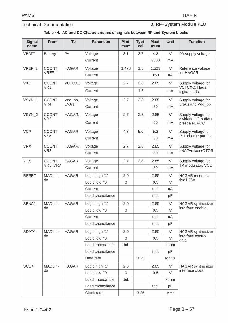
PAMS
Technical Documentation
RAE-5
3. RF+System Module KL8
Page 3 – 57Issue 1 04/02
Table 44. AC and DC Characteristics of signals between RF and System blocks
Signalname
From To Parameter Mini-mum
Typi-cal
Maxi-mum
Unit Function
VBATT Battery PA Voltage 3.1 3.7 4.8 V PA supply voltage
Current 3500 mA
VREF_2 CCONTVREF
HAGAR Voltage 1.478 1.5 1.523 V Reference voltagef HAGARVREF
Current 150 uAfor HAGAR
VXO CCONTVR1
VCTCXO Voltage 2.7 2.8 2.85 V Supply voltage forVCTCXO HagarVR1
Current 1.5 mAVCTCXO, Hagardigital parts.
VSYN_1 CCONTVR4
Vdd_bb,LNA’
Voltage 2.7 2.8 2.85 V Supply voltage forLNA’ d Vdd bbVR4 LNA’s
Current 80 mALNA’s and Vdd_bb
VSYN_2 CCONTVR3
HAGAR, Voltage 2.7 2.8 2.85 V Supply voltage fordividers LO buffersVR3
Current 50 mAdividers, LO buffers,prescaler, VCO
VCP CCONTV5V
HAGAR Voltage 4.8 5.0 5.2 V Supply voltage forPLL hV5V
Current 30 mAPLL charge pumps
VRX CCONTVR2
HAGAR, Voltage 2.7 2.8 2.85 V Supply voltage forLNA2 i DTOSVR2
Current 80 mALNA2+mixer+DTOS
VTX CCONTVR5 VR7
HAGAR Voltage 2.7 2.8 2.85 V Supply voltage forTX d l t VCOVR5, VR7
Current 80 mATX modulator, VCO
RESET MADLin-d
HAGAR Logic high ”1” 2.0 2.85 V HAGAR reset, ac-ti LOWda
Logic low ”0” 0 0.5 Vtive LOW
Current tbd. uA
Load capacitance tbd. pF
SENA1 MADLin-d
HAGAR Logic high ”1” 2.0 2.85 V HAGAR synthesizeri t f blda
Logic low ”0” 0 0.5 Vinterface enable
Current tbd. uA
Load capacitance tbd. pF
SDATA MADLin-d
HAGAR Logic high ”1” 2.0 2.85 V HAGAR synthesizeri t f t lda
Logic low ”0” 0 0.5 Vinterface controldata
Load impedance tbd. kohmdata
Load capacitance tbd. pF
Data rate 3.25 Mbit/s
SCLK MADLin-d
HAGAR Logic high ”1” 2.0 2.85 V HAGAR synthesizeri t f l kda
Logic low ”0” 0 0.5 Vinterface clock
Load impedance tbd. kohm
Load capacitance tbd. pF
Clock rate 3.25 MHz

PAMS
Technical Documentation
RAE-5
3. RF+System Module KL8
Page 3 – 58 Issue 1 04/02
Table 44. AC and DC Characteristics of signals between RF and System blocks (continued)
FunctionUnitMaxi-mum
Typi-cal
Mini-mum
ParameterToFromSignalname
TXP MADLin-d
HAGAR Logic high ”1” 2.0 2.85 V Transmitter powert l blda
Logic low ”0” 0 0.5 Vcontrol enable
Load Resistance 10 220 kohm
Load Capacitance 20 pF
AFC COBBA VCTCXO Voltage 0.046 2.254 V Automatic frequen-t l i l f
Resolution 11 bitscy control signal forVCTCXO
Load resistance(dynamic)
10 kohmVCTCXO
Load resistance(static)
1 Mohm
Noise voltage 500 uVrms 10...10000Hz
Settling time 0.5 ms
RFC VCTCXO MADLin-d
Frequency 13/26 MHz High stability clocki l f th l ida
Signal amplitude 0.5 1.0 2.0 Vppsignal for the logiccircuits in the sys-
Load resistance 10 kohmcircuits in the system block
Load capacitance 10 12 14 pF
RXIP HAGAR COBBA Output level 300 1400 mVpp Single ended in–h RX i l t
Source imped-ance
10 kohmphase RX signal tobaseband
Load resistance 1 Mohm
Load capacitance 8 pF
RXQP HAGAR COBBA Output level 300 1400 mVpp Single ended quad-t RX i l t
Source imped-ance
10 kohmrature RX signal tobaseband
Load resistance 1 Mohm
Load capacitance 8 pF
RXREF COBBA HAGAR Voltage 1.15 1.2 1.25 V Reference voltagef RX b b d
Source imped-ance
200 ohmfor RX basebandsignals
Current 50 uA

PAMS
Technical Documentation
RAE-5
3. RF+System Module KL8
Page 3 – 59Issue 1 04/02
Table 44. AC and DC Characteristics of signals between RF and System blocks (continued)
FunctionUnitMaxi-mum
Typi-cal
Mini-mum
ParameterToFromSignalname
TXIP/TXIN
COBBA HAGAR Differential voltageswing (x0.75)
1.226 1.32 1.416 Vpp Differential in–phaseTX baseband signalf th TX I/Q dDC level 1.165 1.2 1.235 V for the TX I/Q mod-ulator. Note: swing
Differential offsetvoltage (cor-rected)
+/–2.0 mVulator. Note: swingmultiplier maychange later
Diff. offset voltagetemp. depen-dence
+/–5.0 mV
Source imped-ance
500 ohm
Load resistance 40 kohm
Load capacitance 10 pF
Resolution 8 bits
TXQP/TXQN
COBBA HAGAR Differential voltageswing (x0.75)
1.226 1.32 1.416 Vpp Differential quadra-ture TX basebandi l f th TX I/QDC level 1.165 1.2 1.235 V signal for the TX I/Q
modulator. Note:Differential offsetvoltage (cor-rected)
+/–2.0 mVmodulator. Note:swing multiplier 0.75may change later
Diff. offset voltagetemp. depen-dence
+/–5.0 mV
Source imped-ance
500 ohm
Load resistance 40 kohm
Load capacitance 10 pF
Resolution 8 bits
TXC COBBA HAGAR Voltage Min 0.12 0.18 V Transmitter powert l lt
Voltage Max 2.27 2.33 Vcontrol voltage
Vout temperaturedependence
+/–50 ppm/°C
Source imped-anceactive state
200 ohm
Input resistance 10 kohm
Input capacitance 10 pF
Settling time 10 us
Noise level 500 uVrms 0...200 kHz
Resolution 10 bits

PAMS
Technical Documentation
RAE-5
3. RF+System Module KL8
Page 3 – 60 Issue 1 04/02
Timings
Transmit power Timing
Figure 14. Transmitter control timing diagram for all kind of TX bursts
Pout
TXC
TXP
542.8 us
Modulator power
Controlwritings
min 340us
or two bursts
one burst
1 34
5 7
unknown
Synthesizer clocking
Synthesizers are controlled via serial control bus, which consists of SDATA,SCLK and SENA1 signals. These lines form a synchronous data transfer line.SDATA is for the data bits, SCLK is 3.25 MHz clock and SENA1 is latch enable,which stores the data into counters or registers. The signal SENA1 is latch en-able also for HAGAR control register, which is used for programming some in-ternal functions in HAGAR, e.g. in band changing. In this case SCLK and SDA-TA are used the same way as in PLL programming.
Table 45. Internal antenna connector
Parameter Min. Min. Typ. Max. Unit/Notes
Operating frequency range 880 880 1880 MHz
Insertion loss in GSM band 0.2 dB
Insertion loss in DCS band 0.4 dB
[] 1

PAMS Technical DocumentationRAE-5 Series PDA
Issue 1 04/02 Copyright 2001. Nokia Mobile Phones. All Rights Reserved.
4. User Interfaces

PAMS
Technical Documentation
RAE-5
4. User Interfaces
Page 4 – 2 Issue 1 04/02
AMENDMENT RECORD SHEET
AmendmentNumber
Date Inserted By Comments
04/02 OJuntunen

PAMS
Technical Documentation
RAE-5
4. User Interfaces
Page 4 – 3Issue 1 04/02
CONTENTS –Troubleshooting
Page NoAbbreviations 4. . . . . . . . . . . . . . . . . . . . . . . . . . . . . . . . . . . . . . . .
RAE-5 User Interface Structure 5. . . . . . . . . . . . . . . . . . . . . . . . . . .
User Interface DL2 5. . . . . . . . . . . . . . . . . . . . . . . . . . . . . . . . . . . . . .
Main Components 6. . . . . . . . . . . . . . . . . . . . . . . . . . . . . . . . . . DC Characteristics 6. . . . . . . . . . . . . . . . . . . . . . . . . . . . . . . . .
Connections 6. . . . . . . . . . . . . . . . . . . . . . . . . . . . . . . . . . . . . . . . . X1 connector pinout 7. . . . . . . . . . . . . . . . . . . . . . . . . . . . . . . . Antenna clip connector 9. . . . . . . . . . . . . . . . . . . . . . . . . . . . . . X2 connector pinout 9. . . . . . . . . . . . . . . . . . . . . . . . . . . . . . . . X3 connector pinout 10. . . . . . . . . . . . . . . . . . . . . . . . . . . . . . . . X6 connector pinout 11. . . . . . . . . . . . . . . . . . . . . . . . . . . . . . . . X7 connector pinout 11. . . . . . . . . . . . . . . . . . . . . . . . . . . . . . . . RF connection 12. . . . . . . . . . . . . . . . . . . . . . . . . . . . . . . . . . . . .
Functional description 13. . . . . . . . . . . . . . . . . . . . . . . . . . . . . . . . . . .
Power distribution and control signals 13. . . . . . . . . . . . . . . . . DL2 Circuit Description 14. . . . . . . . . . . . . . . . . . . . . . . . . . . . . . . .
Keypad scanning. 14. . . . . . . . . . . . . . . . . . . . . . . . . . . . . . . . . . CMT keypad and CMT LCD backlight 14. . . . . . . . . . . . . . . . . CMT LCD 14. . . . . . . . . . . . . . . . . . . . . . . . . . . . . . . . . . . . . . . . . PDA LCD Module . 15. . . . . . . . . . . . . . . . . . . . . . . . . . . . . . . . . PDA LCD Backlight circuit 15. . . . . . . . . . . . . . . . . . . . . . . . . . . PDA LCD Power circuit 16. . . . . . . . . . . . . . . . . . . . . . . . . . . . . Antenna connectors and ground plane 17. . . . . . . . . . . . . . . .
QWERTY Keyboard Module UL8 18. . . . . . . . . . . . . . . . . . . . . . . . .
General 18. . . . . . . . . . . . . . . . . . . . . . . . . . . . . . . . . . . . . . . . . . . . . AF8 PWB 19. . . . . . . . . . . . . . . . . . . . . . . . . . . . . . . . . . . . . . . . . . . .

PAMS
Technical Documentation
RAE-5
4. User Interfaces
Page 4 – 4 Issue 1 04/02
Abbreviations
AC Alternating CurrentBOC Blue Oyster CultCMT Cellular Mobile TransceiverCCFL Cold Cathode Fluorescent LampDL2 Linda Display module including PWB and displaysESD Electro Static DischargeFPC Flexible Printed CircuitFSTN Film Compensated Super Twisted NematicKL8 RAE–5 Main PWBLCD Liquid Crystal DisplayLED Light Emitting DiodeMCU Micro Computer UnitPWB Printed Wiring BoardPDA Personal Digital AssistantUI User InterfaceUIF User InterFaceUL2 DL2 PWB submodule

PAMS
Technical Documentation
RAE-5
4. User Interfaces
Page 4 – 5Issue 1 04/02
RAE-5 User Interface Structure
RAE–5 GSM900/GSM1800 Dual Band Communicator User Interface com-prises the QWERTY keyboard module UL8 and the DL2 module with both dis-plays.
User Interface DL2
This section describes the DL2 module. This module includes – a PWB (UL2) with SMD components, – PDA display (including CCFL backlight), – CMT display with frame and lightguide and – CMT keypad backlights.
DL2 is located in the cover side of RAE–5. Figures below describe the twosides of the module.

PAMS
Technical Documentation
RAE-5
4. User Interfaces
Page 4 – 6 Issue 1 04/02
Figure 1. DL2 module
Main Components
DL2 main components include UL2 PWB with components, PDA display andCMT display.
Components on the module assembly include the following:
– Four layer, 0.6mm thick PWB (UL2) including:
– PDA LCD CCFL backlight circuit.
– Power circuit for PDA LCD bias voltages.
– Power circuit and LEDs for CMT keypad and CMT display back-light.
– Antenna clips and ground plane.
– Coaxial cable connector for antenna cable.
– 10–pin and 20–pin flex connectors for PDA display module.

PAMS
Technical Documentation
RAE-5
4. User Interfaces
Page 4 – 7Issue 1 04/02
– 50–pin flex connector for hinge flex.
– 10–pin flex connection for CMT display.
– 4–way stacker connection for piezo flex assembly.
– Pads for CMT keypad.
– PDA soft key switches.
– PDA LCD module including lightguide, piezo transformer FPC, CCFL andmetal frame.
– CMT Display module including metal frame and lightguide.
DC Characteristics
Supply voltages and power consumption are listed below:
Pin /Conn.
Line Sym-bol
Parameter Minimum Typical Maximum Unit Notes
X1/1,X1/49,X1/50
VB Battery Volt-age
3.0 3.6 4.2 V 4.8V Absolutemaximum
X1/50 210 mA
X1/11 VBB Logic voltage 2.7 2.8 2.9 V
20 mA
Connections
The 50–way FPC connects the DL2 to the KL8 (system logic and RF board) viathe hinge. It has all active signals for the DL2 module and supply pins. It isconnected to the 50–pin board–to–board connector X1.
DL2 has coaxial cable connector for antenna cable. This co–axial cable goesthrough the hinge to the KL8 RF part.
X1 connector pinout
PIN/Pins
Line Sym-bol
Parameter Min. Typ./
Nom.
Max. Unit Activelevel
Function
1,4950
VB Battery voltage 3.0 3.6 4.2 V Supply
11 VBB Logic voltage 2.7 2.8 2.9 V Supply
3, 7,19, 26,37, 38,44, 48
GND Ground 0 V Supply
21 LCDPWR PDA LCD Volt-ages switch
01.58V
0.88VVBB
V InactiveActive
Input. Highlevel turnson supplyto display

PAMS
Technical Documentation
RAE-5
4. User Interfaces
Page 4 – 8 Issue 1 04/02
FunctionActivelevel
UnitMax.Typ./
Nom.
Min.ParameterLine Sym-bol
PIN/Pins
16 GenSClk Serial Clock forCMT di l
0 3.25 4.0 MHz InputCMT display
00.7xVBB
0.3xVBBVBB
V LowHigh
Input
18 GenSDIO Serial Data forCMT display
00.7xVBB
0.3xVBBVBB
V LowHigh
Input
46 Row5LCDCD
CMT display con-trol / data
00.7xVBB
0.3xVBBVBB
V ControlData
Input. Lowlevel se-lects com-mand regis-ter
15 LCDEN CMT display en-able
00.7xVBB
0.3xVBBVBB
V ActiveInactive
Input. Lowlevel en-ables writ-ing to thedisplay
13 LCDRSTX CMT display reset 00.7xVBB
0.3xVBBVBB
V ActiveInactive
Input. Lowlevel resetsthe display
14 KBLIGHTS CMT keypad anddisplay backlightcontrol
00.7xVBB
0.3xVBBVBB
V ActiveInactive
Input. Highlevel turnslights on.
22 LCDDa0 PDA display data 01.58V
0.88VVBB
V LowHigh
Input
2 LCDDa1 PDA display data 01.58V
0.88VVBB
V LowHigh
Input
4 LCDDa2 PDA display data 01.58V
0.88VVBB
V LowHigh
Input
33 LCDDa3 PDA display data 01.58V
0.88VVBB
V LowHigh
Input
8 LCDDa4 PDA display data 01.58V
0.88VVBB
V LowHigh
Input
31 LCDDa5 PDA display data 01.58V
0.88VVBB
V LowHigh
Input
32 LCDDa6 PDA display data 01.58V
0.88VVBB
V LowHigh
Input
6 LCDDa7 PDA display data 01.58V
0.88VVBB
V LowHigh
Input
9 LCDDa8 PDA display data 01.58V
0.88VVBB
V LowHigh
Input
5 LCDDa9 PDA display data 01.58V
0.88VVBB
V LowHigh
Input
34 LCDDa10 PDA display data 01.58V
0.88VVBB
V LowHigh
Input

PAMS
Technical Documentation
RAE-5
4. User Interfaces
Page 4 – 9Issue 1 04/02
FunctionActivelevel
UnitMax.Typ./
Nom.
Min.ParameterLine Sym-bol
PIN/Pins
20 LCDDa11 PDA display data 01.58V
0.88VVBB
V LowHigh
Input
25 DISPClk PDA display Pixell k
8 8.66 10 MHzclock
01.58V
0.88VVBB
V LowHigh
Input
35 LLClk PDA display Linel
0 10.8 12.5 kHzpulse
01.58V
0.88VVBB
V LowHigh
Input
23 FSP PDA displayF l
0 51.5 59 HzFrame pulse
01.58V
0.88VVBB
V LowHigh
Input
10 LCDM PDA display AC–d l ti
0 10.8 15 kHzmodulation
01.58V
0.88VVBB
V LowHigh
Input
24 DISPON PDA display ON/OFF
01.58V
0.88VVBB
V ActiveInactive
Input
36 LCD_TEMP
Connected toground for colordisplay detection.
Unused.
30 Col0 Keypad column 0 00.7xVBB
0.3xVBBVBB
V LowHigh
Input
27 Col1 Keypad column 1 00.7xVBB
0.3xVBBVBB
V LowHigh
Input
28 Col2 Keypad column 2 00.7xVBB
0.3xVBBVBB
V LowHigh
Input
43 Col3 Keypad column 3 00.7xVBB
0.3xVBBVBB
V LowHigh
Input
45 Col4 Keypad column 4 00.7xVBB
0.3xVBBVBB
V LowHigh
Input
29 Row0 Keypad row 0 00.7xVBB
0.3xVBBVBB
V LowHigh
Output
39 Row1 Keypad row 1 00.7xVBB
0.3xVBBVBB
V LowHigh
Output
40 Row2 Keypad row 2 00.7xVBB
0.3xVBBVBB
V LowHigh
Output
41 Row3 Keypad row 3 00.7xVBB
0.3xVBBVBB
V LowHigh
Output

PAMS
Technical Documentation
RAE-5
4. User Interfaces
Page 4 – 10 Issue 1 04/02
FunctionActivelevel
UnitMax.Typ./
Nom.
Min.ParameterLine Sym-bol
PIN/Pins
42 Row4 Keypad row 4 00.7xVBB
0.3xVBBVBB
V LowHigh
Output
17 LCDPWM PDA LCD Con-trast control
00.7xVBB
50.7
0.3xVBBVBB
V
KHz
LowHigh
Input
47 BACKPWM PDA LCD Back-light control
00.7xVBB
335
0.3xVBBVBB
V
Hz
LowHigh
Input
Antenna clip connector
DL2 has antenna clips that are connected to the antenna.
Pin LineSymbol
Parame-ter
Minimum Typical /Nominal
Maxi-mum
Unit Notes
X1/1,X1/49,X1/50
VB BatteryVoltage
3.0 3.6 4.2 V 4.8V Ab-solutemaximum
X002 connector pinout
Row driver features a 10–pin flex connector.
Pin LineSym-bol
Minimum Typical / Nomi-nal
Maximum Unit Notes
1 GND 0 V LCD driving level for Ydriver IC
2 XINH 00.8 x VDDY
Logic 0Logic 1
0.2 x VDDYVDDY
V Line sub–sampling signalfor Y driver IC
3 YSCL 00.9 x VDDY
Logic 0Logic 1
0.1 x VDDYVDDY
V Shift clock for Y driver IC
4 FRY 00.8 x VDDY
Logic 0Logic 1
0.2 x VDDYVDDY
V Output control for Y driverIC
5 VCCY 2.7 VCC–V5Y3.3
4.5 V High level supply voltagefor Y driver IC
6 V5Y Low level supply voltagefor Y driver IC
7 NC Not connected

PAMS
Technical Documentation
RAE-5
4. User Interfaces
Page 4 – 11Issue 1 04/02
NotesUnitMaximumTypical / Nomi-nal
MinimumLineSym-bol
Pin
8 V0Y 8.0 V0Y–V5Y–VDD 33 V LCD driving level for Ydriver IC
9 VDD LCD driving level for Ydriver IC
10 DY 00.8 x VDDY
Logic 0Logic 1
0.2 x VDDYVDDY
Shift start pulse for Y driv-er IC
X003 connector pinout
Column drivers feature a 20–pin flex connector.
Pin Line Symbol Minimum Typical / Nom-inal
Maximum Unit Notes
1 VCC V Logic supply for X driver
2 VDDH V LCD supply for X driver
3 D23 00.7 x VDDX
Logic 0Logic 1
0.3 x VDDXVDDX
V Digital video signal
4 D22 00.7 x VDDX
Logic 0Logic 1
0.3 x VDDXVDDX
V Digital video signal
5 D21 00.7 x VDDX
Logic 0Logic 1
0.3 x VDDXVDDX
V Digital video signal
6 D20 00.7 x VDDX
Logic 0Logic 1
0.3 x VDDXVDDX
V Digital video signal
7 GCP 00.7 x VDDX
Logic 0Logic 1
0.3 x VDDXVDDX
V PWM width controlpulse for X driver
8 FR 00.7 x VDDX
Logic 0Logic 1
0.3 x VDDXVDDX
V Output alternation signalfor X drivers
9 LP 00.7 x VDDX
Logic 0Logic 1
0.3 x VDDXVDDX
V Data load and shiftpulse for X driver
10 RES 00.7 x VDDX
Logic 0Logic 1
0.3 x VDDXVDDX
V PWM counter reset sig-nal for X driver
11 D03 00.7 x VDDX
Logic 0Logic 1
0.3 x VDDXVDDX
V Digital video signal
12 D02 00.7 x VDDX
Logic 0Logic 1
0.3 x VDDXVDDX
V Digital video signal
13 D01 00.7 x VDDX
Logic 0Logic 1
0.3 x VDDXVDDX
V Digital video signal
14 D00 00.7 x VDDX
Logic 0Logic 1
0.3 x VDDXVDDX
V Digital video signal

PAMS
Technical Documentation
RAE-5
4. User Interfaces
Page 4 – 12 Issue 1 04/02
NotesUnitMaximumTypical / Nom-inal
MinimumLine SymbolPin
15 XSCL 00.7 x VDDX
Logic 0Logic 1
0.3 x VDDXVDDX
V Shift clock for X driver
16 D13 00.7 x VDDX
Logic 0Logic 1
0.3 x VDDXVDDX
V Digital video signal
17 D12 00.7 x VDDX
Logic 0Logic 1
0.3 x VDDXVDDX
V Digital video signal
18 D11 00.7 x VDDX
Logic 0Logic 1
0.3 x VDDXVDDX
V Digital video signal
19 D10 00.7 x VDDX
Logic 0Logic 1
0.3 x VDDXVDDX
V Digital video signal
20 GND 0 V Logic Low signal for Xdriver,LCD low level for X driv-er
X006 connector pinout
X006 is a 4 way ’stacker’ connector to piezo FPC.
Pin Line Sym-bol
Parameter Mini-mum
Typical/ Nomi-
nal
Maxi-mum
Unit Function
1 Feedback Feedback from CCFLoutput
0 0.84 1.54 V Input
2 Piezo_in Input to primary of pie-zo transformer
0 5 8 Vrms Output
3 AGND 0 V Supply
4 GND 0 V Supply
X007 connector pinout
X007 is a 10 way flex connector to CMT LCD..
Pin Line Sym-bol
Parameter Mini-mum
Typical/ Nomi-
nal
Maxi-mum
Unit Notes Function
1 GND Ground 0 V Supply
2 VOUT DC/DC voltage con-verter output
9 Input
3 LCDRSTX Reset 0 0.3xVBB Active Output
4,5 VBB Supply voltage 2.7 2.8 2.9 V Supply
300 uA
6 GenSClk Serial clock input 203kHz 3.25MHz
3.25MHz MHz Output

PAMS
Technical Documentation
RAE-5
4. User Interfaces
Page 4 – 13Issue 1 04/02
FunctionNotesUnitMaxi-mum
Typical/ Nomi-
nal
Mini-mum
ParameterLine Sym-bol
Pin
6 00,7xVBB
0.3xVBBVBB
V LowHigh
Output
7 GenSDIO Serial data input 0 0.3xVBB V Low Output
0.7xVBB VBB V High
8 Row5LCDCD
Control/display dataflag input
0 0.3xVBB Control Output
0.7xVBB VBB Data
9 LCDEN Chip select input 0 0.3xVBB Active Output
0.7xVBB VBB Inactive
10 OSC* External clock forLCD
Connected toVBB on UL2
Inactive
RF connection
Pin Linesymbol
Parameter Minimumfrequency
Maximumfrequency
Maximum power Notes
RF Antenna feedcable
890 MHz 1880 MHz 33 dBm (peak) 28.8 dBm (average)

PAMS
Technical Documentation
RAE-5
4. User Interfaces
Page 4 – 14 Issue 1 04/02
Functional description
Power distribution and control signals
The following block diagram describes the distribution of power supplies withinDL2.
Battery voltage VB is fed directly to the illumination LEDS (CMT keymat andCMT display)
The regulated band supply VBB generated on the KL8 module supplies theCMT display, control logic and PDA display supply.
A power switch is used to remove the voltage supply from the control logic andPDA display when the display is turned off.
Figure 2. Power distribution and control signals of UL2.
PDA LCDbacklight
Keyboardbacklight backlight
CMTLCD
PDA LCD Bias power
VB
VBB
GND
KBLIGHTSBACKPWM
and control logicCMT LCD
16mA typ
110mA 20mA typ 10mA typ
300uA maxtypical
LCDPWR

PAMS
Technical Documentation
RAE-5
4. User Interfaces
Page 4 – 15Issue 1 04/02
DL2 Circuit Description
The module is connected via a 50 way FPC to the KL8 system logic.
The module includes following main blocks:
– CMT keyboard geometries.
– Switches for PDA soft keyboard
– Backlight LEDs for CMT keypad and CMT LCD illumination.
– CMT LCD.
– PDA LCD module.
– PDA LCD backlight circuit.
– PDA LCD power circuit.
– PDA LCD interface control logic.
– Hinge flex connector.
– Antenna connector and ground plane.
Keypad scanning.
There is 26 keys located in DL2 module. 6 PDA soft keys are located inside thelid and 20 CMT keys on the outer side. All these keys are in the same keyboardmatrix as the QWERTY–keypad in the UL8 module.
Col(0–4) are used as column lines in keypad. Row(0–4 and 6) are used as rowlines.
When a key is pressed the MCU gets an interrupt from a row and starts scan-ning. One column at a time is written low and rows are used to read which keyis pressed.
CMT keypad and CMT LCD backlight
The CMT keypad and CMT display are illuminated with LEDs. Each LED isdriven by a separate drive transistor.
LEDs for CMT display are driven with appoximately 5mA each.
LEDs for CMT keymat illumination are driven with approximately 2.5mA each.
CMT LCD
Mechanical structure
LCD includes the frame, LCD cell with driver chip, reflector, adhesive tapes,and lightguide. The LCD is electrically connected to the UL2 PWB with a FPCand board–to–board connector.

PAMS
Technical Documentation
RAE-5
4. User Interfaces
Page 4 – 16 Issue 1 04/02
The frame includes clips to mechanically attach the display to the UL2 PWBand also keep LCD cell and lightguide in place.
LCD cell specification
The LCD cell includes the display driver.
PDA LCD Module .
PDA LCD circuit main blocks are LCD glass including drivers, PDA LCD biasvoltage power circuit and a control IC.
Parameter Function
Display resolution 640 (x3) x 200 dots
Active area 107.52 x 33.6
Dot pitch 0.168 x 0.168mm
Display mode D–TFD, Color, Transmissive
Frame frequency 51.5 Hz typical
Colors 4096 colors, 12–bit RGB
Display brightness 100nit (full brightness typical)
PDA LCD Backlight circuit
Figure 3. Backlight Power Supply
Controlcircuit Driver
Piezotransformer CCFL
VB
VBB
BACKPWM
DISPON
The control circuit generates a square wave input to the piezo driver circuit.This signal is maintained at the resonant frequency of the piezo transformer.
The driver is based around 2 FETs in Push–pull configuration. There is a singlecoil between the FETs and the piezo transformer.
Both FETs are turned off while the CCFL is off during dimming (BACKPWMlow).

PAMS
Technical Documentation
RAE-5
4. User Interfaces
Page 4 – 17Issue 1 04/02
The piezo transformer part is soldered onto a FPC with the CCFL.
Piezo transformer characteristic Value
Input voltage 8Vrms Max
Output power 1 W max
Output voltage 200 Vrms min
Output current 4.5mA
Operating current 1.5mA nominal
Operating frequency 130 +/– 10 kHz
The CCFL lamp is 2.6mm outer diameter and 1.8 mm inner diameter Doubletube.
CCFL lamp characteristic Value
Operating frequency 150 kHz (typ.)
Starting Voltage About 500 Vrms
Operating Voltage 200 Vrms
Tube current 1 mA min , 3mA max
Operating current 1.5mA
CCFT Lamp and Piezo unit I078 par no. 4850183
Figure 4. CCFT Lamp and piezo unit reference number
PDA LCD Power circuit
PDA LCD power circuit generates the bias voltages necessary for the PDA dis-play panel. Block diagram below.

PAMS
Technical Documentation
RAE-5
4. User Interfaces
Page 4 – 18 Issue 1 04/02
Figure 5. Block diagram of PDA Power Supply
VCC
LCDPWM
DY
V0Y
V5Y
VCCY
FRY
YSCL
XINH
Control ASIC
Flyback Regulator
Swing ModeRegulator
Data Synchronisation
The flyback regulator generates a negative bias voltage (Nominally –12V) fromthe battery voltage. The output of the flyback generator is temperature compen-sated and adjusted under software control.
The control ASIC handles the refresh of data to the PDA display panel and thegeneration of synchronisation signals for the swing mode regulator.
Antenna connectors and ground plane
The RF–signal from the external antenna connector/switch on KL8 is fed to theantenna via a coaxial cable that is led through the hinge. The signal is fed tothe antenna through a coaxial connector and an antenna clip which are placedon the UL2 PWB.
The UL2 PWB includes the separate ground area that is required by the anten-na.

PAMS
Technical Documentation
RAE-5
4. User Interfaces
Page 4 – 19Issue 1 04/02
QWERTY Keyboard Module UL8
General
UL8 is the combined QWERTY keypad/flex connection module. The base flexis single–sided, so all the components are on the same side of the flex.
Approximate component placement is shown below:
Figure 6. Component placement
70 pin connector 5469145
50 pin connector 5469817
AF8 PWB

PAMS
Technical Documentation
RAE-5
4. User Interfaces
Page 4 – 20 Issue 1 04/02
AF8 PWB
AF8 is a small additional PWB to achieve ”bulls eye” shaped pads for the ear-piece and connection for the battery removal switch. (Check that the RAE-5software supports the battery removal switch feature.)
The approximate shape of AF8 is shown below.
One 22pF SMD capacitor is assembled to the AF8.
Figure 7. AF8 PWB

PAMS Technical DocumentationRAE-5 Communicator
Issue 1 04/02 Copyright 2002. Nokia Corporation. All Rights Reserved.
5. RAE-5 Variants

PAMS
Technical Documentation
RAE-5
5. RAE-5 Variants
Page 5 – 2 Issue 1 04/02
AMENDMENT RECORD SHEETAmendmentNumber
Date Inserted By Comments
02/02 OJuntunen

PAMS
Technical Documentation
RAE-5
5. RAE-5 Variants
Page 5 – 3Issue 1 04/02
CONTENTS –Troubleshooting
Page No
Foreword 4. . . . . . . . . . . . . . . . . . . . . . . . . . . . . . . . . . . . . . . . . . . . . .
Country versions 5. . . . . . . . . . . . . . . . . . . . . . . . . . . . . . . . . . . . . Common Modules 5. . . . . . . . . . . . . . . . . . . . . . . . . . . . . . . . . . . .

PAMS
Technical Documentation
RAE-5
5. RAE-5 Variants
Page 5 – 4 Issue 1 04/02
Foreword
This section of the service manual contains information about the RAE-5 PDAvariants.
Various language versions of RAE–5 are supported using different keymats anddifferent FLASH software. All other components (modules & mechanics ) areidentical.
A detailed exploded diagram is available in Section 10, Parts lists.

PAMS
Technical Documentation
RAE-5
5. RAE-5 Variants
Page 5 – 5Issue 1 04/02
Country versions
Table 1. Country versions
Prod-uctcode
Producttype
Variantname
Lan-guage
Keyboard,code
Swapunitcode
Sales area
0630529 RAE–5NA English English EN–QWERTY9790431
0069401 UK, S/A, Easternbloc
0630553 RAE–5NB German German DE–QWERTZ9790503
0069402 Germany
0630554 RAE–5NC French French FR–AZERTY9790505
0069403 FR, Benelux
0630555 RAE–NS Finnish Finnish SCAND9790504
0069411 Finland
0630556 RAE–5NE Swedish Swedish SCAND9790504
0069406 Sweden
0630557 RAE–5NM Danish Danish SCAND9790504
0069413 Denmark
0630558 RAE–5NN Norwegian Norwe-gian
SCAND9790504
0069410 Norway
0630559 RAE–5NX Scandina-vian
English SCAND9790504
0069404 Scand. Countries
0630560 RAE–5NP Dutch Dutch EN–QWERTY9790431
0069409 NL, Benelux
0630561 RAE–5NR Italian Italian IT–QWERTY9790506
0069405 IT
0630562 RAE–5NU APAC English EN–QWERTY9790431
The whole APAC(except China &
Taiwan?)0630563 RAE–5NF Spanish Spanish, ES/PT–
QWERTY9790507
0069407 Spain
0630564 RAE–5NG Portuguese Portu-guese
ES/PT–QWERTY9790507
0069412 Portugal
0630565 RAE–5NH German,ALS acti-
vated
German DE–QWERTZ9790503
0069419 AUT, Switzerland
0630566 RAE–5NY Russia English EN–QWERTY9790431
0069418 Russia
0630567 RAE–5NV Hungary Hungary HU–QWERTY9790588
0069417 Hungary
0630568 RAE–5NZ EnglishPoland
English EN–QWERTY9790431
0069415 Poland
0630569 RAE–5NJ Polish Polish EN–QWERTY9790431 0069416
Poland
0630570 RAE–5NQ Czech Czech CZ–QWERTY9790587
0069414 Czech
0630571 RAE–5NW EnglishTurkey
English EN–QWERTY9790431
0069420 Turkey
0630572 RAE–5NT Turkish Turkish TR–9790508
0069408 TR

PAMS
Technical Documentation
RAE-5
5. RAE-5 Variants
Page 5 – 6 Issue 1 04/02
Main Modules
Unit/type: Product type Productcode:
Modulecode:
• RF&System module KL8 module n.a.
• Keyboard & hinge module UL8 0201667
• UI module without LCDs UL2 0201785
• PDA Colour LCD 4850167
• Mechanics MRAE3 0261997

PAMS Technical DocumentationRAE-5 Series PDA
Issue 1 04/02 Copyright 2002. Nokia Corporation. All Rights Reserved.
6. Service Tools

PAMS
Technical Documentation
RAE-5
6. Service Tools
Page 6 – 2 Issue 1 04/02
AMENDMENT RECORD SHEET
AmendmentNumber
Date Inserted By Comments
03/2002 OJuntunen

PAMS
Technical Documentation
RAE-5
6. Service Tools
Page 6 – 3Issue 1 04/02
CONTENTS -Troubleshooting
Page NoModule Jig MJS-14 6 - 5. . . . . . . . . . . . . . . . . . . . . . . . . . . . . . . . . . .
Product Code 6 - 5. . . . . . . . . . . . . . . . . . . . . . . . . . . . . . . . . . . . . . Views of MJS-14 6 - 5. . . . . . . . . . . . . . . . . . . . . . . . . . . . . . . . . . .
User Guide for MJS-14 6 - 7. . . . . . . . . . . . . . . . . . . . . . . . . . . . . . . . . .
Warnings: 6 - 7. . . . . . . . . . . . . . . . . . . . . . . . . . . . . . . . . . . . . . . . . . . Power Source 6 - 7. . . . . . . . . . . . . . . . . . . . . . . . . . . . . . . . . . . . . Flash Mode vs. EPOC Running -mode 6 - 7. . . . . . . . . . . . . . . .
External Connections 6 - 7. . . . . . . . . . . . . . . . . . . . . . . . . . . . . . . . . RF 6 - 7. . . . . . . . . . . . . . . . . . . . . . . . . . . . . . . . . . . . . . . . . . . . . . . System Signals 6 - 7. . . . . . . . . . . . . . . . . . . . . . . . . . . . . . . . . . . . Audio Signals 6 - 7. . . . . . . . . . . . . . . . . . . . . . . . . . . . . . . . . . . . . . Input Terminals 6 - 7. . . . . . . . . . . . . . . . . . . . . . . . . . . . . . . . . . . .
Detection Switches 6 - 7. . . . . . . . . . . . . . . . . . . . . . . . . . . . . . . . . . . Starting 6 - 8. . . . . . . . . . . . . . . . . . . . . . . . . . . . . . . . . . . . . . . . . . . . . Power ON 6 - 8. . . . . . . . . . . . . . . . . . . . . . . . . . . . . . . . . . . . . . . . . . .
Default State 6 - 8. . . . . . . . . . . . . . . . . . . . . . . . . . . . . . . . . . . . . . EPOC Running State 6 - 8. . . . . . . . . . . . . . . . . . . . . . . . . . . . . . .
In Use 6 - 8. . . . . . . . . . . . . . . . . . . . . . . . . . . . . . . . . . . . . . . . . . . . . . Finishing 6 - 8. . . . . . . . . . . . . . . . . . . . . . . . . . . . . . . . . . . . . . . . . . . . Signals in Board to Board Adapter JC4 6 - 10. . . . . . . . . . . . . . . . . . Flash Prommer FPS-8 (Sales Pack) 6 - 11. . . . . . . . . . . . . . . . . . . .
Product Code 6 - 11. . . . . . . . . . . . . . . . . . . . . . . . . . . . . . . . . . . . . . View of FPS-8 6 - 11. . . . . . . . . . . . . . . . . . . . . . . . . . . . . . . . . . . . .
Calibration Unit JBE-2 6 - 12. . . . . . . . . . . . . . . . . . . . . . . . . . . . . . . . . Product Code 6 - 12. . . . . . . . . . . . . . . . . . . . . . . . . . . . . . . . . . . . . . View of JBE-2 6 - 12. . . . . . . . . . . . . . . . . . . . . . . . . . . . . . . . . . . . .
User Guide for JBE-2 6 - 13. . . . . . . . . . . . . . . . . . . . . . . . . . . . . . . . . . . .
Service Operations 6 - 13. . . . . . . . . . . . . . . . . . . . . . . . . . . . . . . . . . . Power Management Calibrations 6 - 13. . . . . . . . . . . . . . . . . . . . . . . Service Car Kit HCL-1 6 - 14. . . . . . . . . . . . . . . . . . . . . . . . . . . . . . . . .
Product Code 6 - 14. . . . . . . . . . . . . . . . . . . . . . . . . . . . . . . . . . . . . . View of HCL-1 6 - 14. . . . . . . . . . . . . . . . . . . . . . . . . . . . . . . . . . . . .
User Guide for HCL-1 6 - 15. . . . . . . . . . . . . . . . . . . . . . . . . . . . . . . . . . .
Connection to Service SW 6 - 15. . . . . . . . . . . . . . . . . . . . . . . . . . . . . Allowed Power Sources 6 - 15. . . . . . . . . . . . . . . . . . . . . . . . . . . . . . . About Tuning 6 - 15. . . . . . . . . . . . . . . . . . . . . . . . . . . . . . . . . . . . . . . . Dummy Service Battery BBL-3B 6 - 16. . . . . . . . . . . . . . . . . . . . . . . .
Product Code 6 - 16. . . . . . . . . . . . . . . . . . . . . . . . . . . . . . . . . . . . . . View of BBL-3 6 - 16. . . . . . . . . . . . . . . . . . . . . . . . . . . . . . . . . . . . .
Dongle/Flash Device FLS-4 (Sales Pack) 6 - 17. . . . . . . . . . . . . . . . . .

PAMS
Technical Documentation
RAE-5
6. Service Tools
Page 6 – 4 Issue 1 04/02
Product Code 6 - 17. . . . . . . . . . . . . . . . . . . . . . . . . . . . . . . . . . . . . . View of FLS-4 6 - 17. . . . . . . . . . . . . . . . . . . . . . . . . . . . . . . . . . . . .
Service Cable SCH-12 6 - 18. . . . . . . . . . . . . . . . . . . . . . . . . . . . . . . . Product Code 6 - 18. . . . . . . . . . . . . . . . . . . . . . . . . . . . . . . . . . . . . . View of SCH-12 6 - 18. . . . . . . . . . . . . . . . . . . . . . . . . . . . . . . . . . . .
D9-D9 Cable AXS-4 6 - 19. . . . . . . . . . . . . . . . . . . . . . . . . . . . . . . . . . Product Code 6 - 19. . . . . . . . . . . . . . . . . . . . . . . . . . . . . . . . . . . . . . View of AXS-4 6 - 19. . . . . . . . . . . . . . . . . . . . . . . . . . . . . . . . . . . . .
MBUS Cable DAU-9C 6 - 20. . . . . . . . . . . . . . . . . . . . . . . . . . . . . . . . . Product Code 6 - 20. . . . . . . . . . . . . . . . . . . . . . . . . . . . . . . . . . . . . . View of DAU-9C 6 - 20. . . . . . . . . . . . . . . . . . . . . . . . . . . . . . . . . . .
MBUS Cable DAU-9S 6 - 20. . . . . . . . . . . . . . . . . . . . . . . . . . . . . . . . . Product Code 6 - 20. . . . . . . . . . . . . . . . . . . . . . . . . . . . . . . . . . . . . . View of DAU-9S 6 - 20. . . . . . . . . . . . . . . . . . . . . . . . . . . . . . . . . . . .
DC Cable SCB-3 6 - 21. . . . . . . . . . . . . . . . . . . . . . . . . . . . . . . . . . . . . Product Code 6 - 21. . . . . . . . . . . . . . . . . . . . . . . . . . . . . . . . . . . . . . View of SCB-3 6 - 21. . . . . . . . . . . . . . . . . . . . . . . . . . . . . . . . . . . . .
Service Cable SCH-8 6 - 21. . . . . . . . . . . . . . . . . . . . . . . . . . . . . . . . . Product Code 6 - 21. . . . . . . . . . . . . . . . . . . . . . . . . . . . . . . . . . . . . . View of SCH-8 6 - 21. . . . . . . . . . . . . . . . . . . . . . . . . . . . . . . . . . . . .
Power ACH-6 6 - 22. . . . . . . . . . . . . . . . . . . . . . . . . . . . . . . . . . . . . . . . Product Code 6 - 22. . . . . . . . . . . . . . . . . . . . . . . . . . . . . . . . . . . . . . Views of ACH-6 6 - 22. . . . . . . . . . . . . . . . . . . . . . . . . . . . . . . . . . . .
SW Security Device PKD-1 6 - 23. . . . . . . . . . . . . . . . . . . . . . . . . . . . Product Code 6 - 23. . . . . . . . . . . . . . . . . . . . . . . . . . . . . . . . . . . . . . View of SW Security Device 6 - 23. . . . . . . . . . . . . . . . . . . . . . . . .
Modular T-adapter 6 - 23. . . . . . . . . . . . . . . . . . . . . . . . . . . . . . . . . . . . Product Code 6 - 23. . . . . . . . . . . . . . . . . . . . . . . . . . . . . . . . . . . . . . View of Modular T-adapter 6 - 23. . . . . . . . . . . . . . . . . . . . . . . . . .
Assembly Jig MJS-78 6 - 24. . . . . . . . . . . . . . . . . . . . . . . . . . . . . . . . . Product Code 6 - 24. . . . . . . . . . . . . . . . . . . . . . . . . . . . . . . . . . . . . . View of Assembly Jig 6 - 24. . . . . . . . . . . . . . . . . . . . . . . . . . . . . . .
Soldering Jig MJS-61 6 - 25. . . . . . . . . . . . . . . . . . . . . . . . . . . . . . . . . Product Code 6 - 25. . . . . . . . . . . . . . . . . . . . . . . . . . . . . . . . . . . . . .

PAMS
Technical Documentation
RAE-5
6. Service Tools
Page 6 – 5Issue 1 04/02
Module Jig MJS-14
The module jig MJS-4 is used for RAE-5 module testing and repairing. Thereare slots for each module in the jig. The jig includes connections for charger,power supply, external RF, audios and FBUS/MBUS. Slots for Memory card andSIM card are also included. This equipment is powered by a laboratory powersource.
Product Code
Module Jig MJS-14: 0770175
Views of MJS-14
Figure 1. MJS-14, the frontside
Seen from left
Seen from rightSeen from front

PAMS
Technical Documentation
RAE-5
6. Service Tools
Page 6 – 6 Issue 1 04/02
Figure 2. MJS-14, the backside
Seen from back
Note: The nominal supply voltage for MJS-14 is +4.0 V.The supply voltage must not exceed +4.1 V.

PAMS
Technical Documentation
RAE-5
6. Service Tools
Page 6 – 7Issue 1 04/02
User Guide for MJS-14
Warnings:
Power Source
Do not connect negative voltage to Voltage IN -terminals.
Do not connect voltages over 4,2 volts to Voltage IN -terminals.
Flash Mode vs. EPOC Running -mode
If you are using Wintesla service software (for flashing or for testing) do not usethe ”Run EPOC” switch. EPOC software is not allowed to be running duringflashing or while software resets are possible (Wintesla connected).
External Connections
RF
For external RF connection there is a SMA jack connector. The connection isdefined to be made with service cable XRF-1.
Attenuation of the RF connection (without XRF-1 cable) is appx. 0,2dB for 900MHz band and 0,4dB for 1800MHz band.
System Signals
For system signal connection (Fbus/Mbus) there is a modular 10 socket in thejig. The socket is compatible also with modular 8 plug. Preferred cables for system connection are XCS-4 and DAU-9S.
Audio Signals
For audio signals the jig includes also a modular 10 socket. SGND is separatedfrom general GND although in ADS-1 service cable specificed for use with thejig those are short-circuited.
Input Terminals
For powering the jig there are two ”banana” sockets. Red one for + terminaland black for GND terminal.
Detection Switches
There are three switches by which different detections can be done. Switchesare press switch type so the connection is made only while the switch ispressed.

PAMS
Technical Documentation
RAE-5
6. Service Tools
Page 6 – 8 Issue 1 04/02
1 S101: Head set detection
2 S102: Hook detection
3 S103: Accessory detection
Starting
Open the cover of the jig and place SIM card and microphone to their places ifneeded.
Then place modules of RAE-5 to proper positions: first KL8 then in order JC4(board to board adapter), UL8 (keymat on it if needed) and (keymat under ifneeded) DL1. Give special attention to connections of board to board connec-tors, connectors are not specified for continuous removing.
Close the cover of the jig.
Turn the jig over.
Connect the flex to UI module.
Place memory card and/or audio holder under its/their covers.
Connect the necessary cables. Jig is ready for use.
Power ON
There are two working modes in jig:
Default State
Entering to default state does not require any user actions. Just turn the powerof the source ON. Symbian software will not run. There is a notification aboutthe state in PDA display. Wintesla service software can be used with jig, differ-ent kind of test cases will work (PDA display test, MMC test, etc.).
EPOC Running State
”Run Symbian” switch is needed to be pressed down while turning the powerON. The switch can be released after the SW has started to boot up. EPOCsoftware will now run.
In Use
For simulation of cover open / cover closed there is a magnet toggle on coverof the jig. Sticker beside the toggle describes the meaning of positions. Themagnetic force (field strength) is a bit weaker than in Linda communicator.
There are extra GNDs included to jc4 board to board adapter. There is also aspecial GND pin in middle of the jig.
Finishing
Before turning the main source off press the nail in audio cover to make an in-terrupt to processor. This is important especially if you have an active call ON

PAMS
Technical Documentation
RAE-5
6. Service Tools
Page 6 – 9Issue 1 04/02
or data transfer going to/from memory card (or serial flash). After pressing thenail down turn the source off within 5 seconds (while PDA display is blanked ifcover open).
Note: Check whether the SW version of the device under test supports thisfunction (battery removal interrupt).

PAMS
Technical Documentation
RAE-5
6. Service Tools
Page 6 – 10 Issue 1 04/02
Signals in Board to Board Adapter JC4
Table 1. Pin List of JC4
Pin Name Description Pin Name Description
1 GND 36 LCDDa5
2 DispClk 8,667MHz 37 LCDDa6
3 DISPON 38 LCDDa3
4 FSP 39 LCDDa10
5 LCDDa0 40 LLClk
6 LCD_PWR 41 GND
7 LCDDa11 42 BATT_REM
8 GND 43 SPKP
9 GenSDIO 44 SPKP
10 LCDPWM 45 SPKN
11 GenSClk 2,16MHz/3,25MHz 46 SPKN
12 LCDEN 47 EARN
13 KBLIGHTS 48 EARP
14 LCDRSTX 49 Col0
15 FLVPP 50 Row0
16 VPROG 51 Col9
17 VBB 52 Row9
18 LCDM 53 Col8
19 LCDDa8 54 Col4
20 LCDDa4 55 Col5
21 GND 56 Col6
22 LCDDa7 57 Row6
23 LCDDa9 58 Row8
24 LCDDa2 59 Col3
25 GND 60 Col2
26 LCDDa1 61 Col7
27 VB 62 Col1
28 VB 63 Row5LCDCD
29 VB 64 Row4
30 GND 65 Row3
31 BackPWM 66 -
32 Row5LCDCD 67 Row2
33 Col4 68 Row7
34 GND 69 Row1
35 Col3 70 GND

PAMS
Technical Documentation
RAE-5
6. Service Tools
Page 6 – 11Issue 1 04/02
Flash Prommer FPS-8 (Sales Pack)
The Flash Prommer FPS-8 is used to update the main software of the phone.Updating is done by first loading the new MCU software from the PC to theflash prommer, and then loading the new SW from the prommer to the phone.When updating more than one phone in succession, the MCU software onlyneeds to be loaded to the prommer once.
The FPS-8 sales pack 0080321 includes:
Item: Service accessory: Type Product code:
1 Flash Prommer FPS-8 07501232 AC/DC Adapter FRIWO 06800323 D9 - D9 Cable AXS-4
(between PC and FPS-8) 07300904 Printer Cable 07300295 Installation software for FPS-8
The following additional memories/modules are available for FPS-8:
- SRAM module (8MB) SF12 0080346. . . . . . . . . . . . . . . .
Note : 2 pcs of SF12 are mandatory for updating RAE-5N software !
- Flash Module (64MB) SF13 0080347. . . . . . . . . . . . . . . . . . . . . (optional). . . . . . . . . . . . . . . . . . . . . . . . . . . . . . . . . . . . . . . . . . . . . . . . . . . . . . . .
Product Code
Flash Prommer FPS-8: 0750123
View of FPS-8

PAMS
Technical Documentation
RAE-5
6. Service Tools
Page 6 – 12 Issue 1 04/02
Calibration Unit JBE-2
Calibration Unit JBE-2 is needed for the resistance, current- and voltage cal-ibrations of a RAE-5 Communicator. These calibrations are needed so that thecharging situation would be precise enough.
NOTE: The JBE-2 is also the voltage source for the BBL-3B service battery. JBE-2 isthe only service equipment which can provide enough current for any servicecase. Power output of FPS-8 flash prommer can not provide enough current incases of tuning and calling and is ment to be used only for flashing purposes.
Product Code
Calibration Unit JBE-2: 0775290
View of JBE-2

PAMS
Technical Documentation
RAE-5
6. Service Tools
Page 6 – 13Issue 1 04/02
User Guide for JBE-2
Service Operations
Needed equipment: a laboratory power source, a calibration unit JBE-2, a ser-vice battery BBL-3B and a service cable DAU-9C.
Use the JBE-2 calibration unit as a power source for the phone. It is the onlyservice tool which can provide needed currents in any service case. The JBE-2is powered by a laboratory power source. Used voltages are 8,0 volts for nor-mal service and 10,5 volts for energy management calibrations. DO NOT con-nect over 12 volts voltage to JBE-2.
With Wintesla service software use service cable DAU-9C. Connect the cablestraight from the PC serial port to the system connector of the phone.
Power Management Calibrations
Needed equipment: a laboratory power source (min 2A out), a calibration unitJBE-2, a service battery BBL-3B, a service cable DAU-9C and a service cableSCB-3.
Use JBE-2 calibration unit as a source for the phone as described in abovesection. Put up the whole calibration environment and turn the phone ON be-fore starting the Wintesla service software. Notice that the less the phone con-sumes current during calibration the more accurate is the result. So you are ad-vised to do the calibrations while PDA display is off (phone SW reset while cov-er closed).

PAMS
Technical Documentation
RAE-5
6. Service Tools
Page 6 – 14 Issue 1 04/02
Service Car Kit HCL-1
The Service Car Kit, HCL-1 is used for RF tuning of a RAE-5 communicator.HCL-1 is modified from CRM-1 car kit. HCL-1 is used as interface betweenRAE-5 and service software (Wintesla) while doing RF tuning and power man-agement.
Note 1: Other needed accessories for RF tuning are Modular T adapter andDAU-9S.
Product Code
Service Car Kit HCL-1: 0770265
View of HCL-1

PAMS
Technical Documentation
RAE-5
6. Service Tools
Page 6 – 15Issue 1 04/02
User Guide for HCL-1
Connection to Service SW
A service car kit HCL-1 is used with a Wintesla service software. Needed ac-cessories are Modular-T-adapter and DAU-9S cable. With these accessoriesthe MBUS is connected straight from the phone to the PC and the necessarylevel transformations are executed.. It is also possible to plug the mod8 con-nector straight to mod10 socket of FPS-8 prommer and control the phonethrough it.
Note that it is not allowed to power the service battery from power outputs ofFPS-8 while using HCL-1.
Allowed Power Sources
BBL-3B service battery is the one for RF tuning. You will also need the JBE-2as power source for the battery. The service battery can also be connectedstraight to laboratory power source. Do not connect a voltage higher than 4,2Vto service battery. There is no advanced high voltage protection in the batteryso you really can damage the phone with voltage too high.
Note: Do not use normal battery BLL-3 while connected to service SW.
About Tuning
Complete instructions how to make the RF tuning itself can be found from ser-vice manual. Remember that connectors and coaxial cable of HCL-1 will causeattenuation to signal approximately as follows:
900MHz band 0.65dB1800MHz band 1.05dB
Note that values may vary a bit from device to device. If you have the equip-ment to define the exact attenuation values for your HCL-1 you are advised todo so.
Note also that the attenuation value is programmed to some tuning equipmentwith positive sign and to some with negative sign (depending on the devicemodel / manufacturer).

PAMS
Technical Documentation
RAE-5
6. Service Tools
Page 6 – 16 Issue 1 04/02
Dummy Service Battery BBL-3B
The Dummy Service Battery BBL-3B (with banana clips) is used in place of thecommunicator’s normal battery during service. The BBL-3B supplies a con-trolled operating voltage from FPS-8 when flashing the Communicator. TheBBL-3B also supplies a controlled operating voltage from JBE-2 when perform-ing resistance, current, voltage or RF calibrations.
NOTE:The service battery can also be connected straight to laboratory powersource. Do not connect a voltage higher than 4,2V to service battery. There isno advanced high voltage protection in the battery so you really can damagethe phone with too high voltage.
Product Code
Dummy Service Battery BBL-3B: 0770206
View of BBL-3

PAMS
Technical Documentation
RAE-5
6. Service Tools
Page 6 – 17Issue 1 04/02
Dongle/Flash Device FLS-4 (Sales Pack)
FLS-4 is a dongle and flash device incorporated into one package, developedspecifically for POS use.
Product Code
FLS-4 Sales Pack -APAC 0081481
View of FLS-4
Features the following connectors::D25 male (visible in pic)USB type B to Host PCMod 10RJ45 to the phoneDC supply for Nokia ACP-8 charger

PAMS
Technical Documentation
RAE-5
6. Service Tools
Page 6 – 18 Issue 1 04/02
Service Cable SCH-12
For use with FLS-4 in flashing.
Product Code
Service Cable SCH-12: 0730137
View of SCH-12

PAMS
Technical Documentation
RAE-5
6. Service Tools
Page 6 – 19Issue 1 04/02
D9-D9 Cable AXS-4
The D9-D9 Cable AXS-4 is used to connect two 9 pin D connectors. e.g. be-tween PC and FPS-8 flash prommer.
Product Code
D9 - D9 Cable AXS-4: 0730090
View of AXS-4

PAMS
Technical Documentation
RAE-5
6. Service Tools
Page 6 – 20 Issue 1 04/02
MBUS Cable DAU-9C
The MBUS Cable DAU-9C has a phone system connector and D9 female. TheDAU9C is MBUS/FBUS interface cable between the phone and PC RS-232 in-terface.
Product Code
MBUS Cable DAU-9C: 0730138
View of DAU-9C
MBUS Cable DAU-9S
The MBUS Cable DAU-9S has a modular connector, and is used between PCand the modular T-adapter.
Product Code
MBUS Cable DAU-9S: 0730108
View of DAU-9S

PAMS
Technical Documentation
RAE-5
6. Service Tools
Page 6 – 21Issue 1 04/02
DC Cable SCB-3
The DC Cable SCB-3 is used to connect the Calibration unit, JBE-1 to thecharger connection Vin of the phone when doing the charger calibration serviceprocedure.
Product Code
DC Cable SCB-3: 0730114
View of SCB-3
Service Cable SCH-8
The Service Cable SCH-8 is used between the phone and FPS-8 and it canused between the phone and modular T-adapter.
Product Code
Service Cable SCH-8: 0730137
View of SCH-8

PAMS
Technical Documentation
RAE-5
6. Service Tools
Page 6 – 22 Issue 1 04/02
Power ACH-6
There are several variants of ACH-6 DC Power sources available:
Product Code
Name of unit Usage area Material code
ACH–6E Europe 0675084
ACH–6U/J U.S.A / Japan 0675085 / 0675140
ACH–6A Australia 0675086
ACH–6X UK / Hong Kong 0675087
Views of ACH-6
ACH–6E ACH–6X
ACH–6U
ACH–6A

PAMS
Technical Documentation
RAE-5
6. Service Tools
Page 6 – 23Issue 1 04/02
SW Security Device PKD-1SW security device is a piece of hardware enabling the use of the service soft-ware when connected to the parallel (LPT) port of the PC. Without the donglepresent it is not possible to use the service software. Printer or any such devicecan be connected to the PC through the dongle if needed.
Caution: Make sure that you have switched off the PC and the printer beforemaking connections!Caution: Do not connected the PKD-1 to the serial port. You may damageyour PKD-1!
Product Code
SW Security Device PKD-1: 0750018
View of SW Security Device
Modular T-adapterThe modular T-adapter is a suitable branching unit to provide the needed paral-lel modular connections.
It is used between the Service Car Kit HCL-1 and DAU-9S.
Product Code
Modular T-adapter: 4626134
View of Modular T-adapter

PAMS
Technical Documentation
RAE-5
6. Service Tools
Page 6 – 24 Issue 1 04/02
Assembly Jig MJS-78
Assembly jig MJS-78 has been developed for assembly and disassembly ofRAE-5.
Product Code
Assembly jig MJS-78: 0770432
View of Assembly Jig

PAMS
Technical Documentation
RAE-5
6. Service Tools
Page 6 – 25Issue 1 04/02
Soldering Jig MJS-61
MJS-61 is a soldering jig for UBGA components .
Product Code
Soldering jig MJS-61 0770373. . . . . . . . . . . . . . . . . .

PAMS
Technical Documentation
RAE-5
6. Service Tools
Page 6 – 26 Issue 1 04/02
This page intentionally left blank.

PAMS Technical DocumentationRAE-5 Series PDA
Issue 1 04/02 Copyright 2002. Nokia Corporation. All Rights Reserved.
7. Service SoftwareInstructions

PAMS
Technical Documentation
RAE-5
7. Service Software Instructions
Page 7 – 2 Issue 1 04/02
AMENDMENT RECORD SHEET
AmendmentNumber
Date Inserted By Comments
04/2002 OJuntunen

PAMS
Technical Documentation
RAE-5
7. Service Software Instructions
Page 7 – 3Issue 1 04/02
CONTENTS –Troubleshooting
Page No
Service Software 7 – 5. . . . . . . . . . . . . . . . . . . . . . . . . . . . . . . . . . . . . . . .
General 7 – 5. . . . . . . . . . . . . . . . . . . . . . . . . . . . . . . . . . . . . . . . . . . . . Hardware requirements for Windows 3.1x 7 – 5. . . . . . . . . . . Hardware requirements for Windows 95 7 – 5. . . . . . . . . . . .
Software Environment of the Support Modules 7 – 5. . . . . . . . . Required Servicing Equipment 7 – 6. . . . . . . . . . . . . . . . . . . . . . . Installation 7 – 7. . . . . . . . . . . . . . . . . . . . . . . . . . . . . . . . . . . . . . . .
Mechanical Connections 7 – 7. . . . . . . . . . . . . . . . . . . . . . . . . . Installing the software on PC Hard Disk 7 – 7. . . . . . . . . . . . .
Common Properties of the User Interface 7 – 8. . . . . . . . . . . . . . . . . .
Login Dialog 7 – 8. . . . . . . . . . . . . . . . . . . . . . . . . . . . . . . . . . . . . . . . . Main Window 7 – 9. . . . . . . . . . . . . . . . . . . . . . . . . . . . . . . . . . . . . . . . Using Help 7 – 9. . . . . . . . . . . . . . . . . . . . . . . . . . . . . . . . . . . . . . . . . .
Software upgrade guide 7 – 10. . . . . . . . . . . . . . . . . . . . . . . . . . . . . . . . .
Equipment Setup instructions 7 – 10. . . . . . . . . . . . . . . . . . . . . . . . . . Setting up the PC 7 – 11. . . . . . . . . . . . . . . . . . . . . . . . . . . . . . . . . . Setting up BUS Configuration for WinTesla 7 – 11. . . . . . . . . . . .
Programming with WinTesla Interface 7 – 12. . . . . . . . . . . . . . . . . . . WinTesla Interface 7 – 12. . . . . . . . . . . . . . . . . . . . . . . . . . . . . . . . . Before programming 7 – 12. . . . . . . . . . . . . . . . . . . . . . . . . . . . . . . . Programming procedure 7 – 12. . . . . . . . . . . . . . . . . . . . . . . . . . . .
ROM/MCU image 7 – 12. . . . . . . . . . . . . . . . . . . . . . . . . . . . . . . . Installing All_Nokia_92XX_data_XX.SIS -package 7 – 18. . . . . .
Troubleshooting for the N9210 SW upgrade 7 – 20. . . . . . . . . . . . . .
Wintesla Tuning 7 – 22. . . . . . . . . . . . . . . . . . . . . . . . . . . . . . . . . . . . . . . .
RF tuning after repairs 7 – 22. . . . . . . . . . . . . . . . . . . . . . . . . . . . . . . . Equipment Setup for RF Tuning without Removing Covers 7 – 23.
RX Calibration 7 – 24. . . . . . . . . . . . . . . . . . . . . . . . . . . . . . . . . . . . . RX Filter Calibration (Automatic) 7 – 27. . . . . . . . . . . . . . . . . . . . . RX AM Suppression (automatic) 7 – 29. . . . . . . . . . . . . . . . . . . . .
EGSM 7 – 29. . . . . . . . . . . . . . . . . . . . . . . . . . . . . . . . . . . . . . . . . . PCN 7 – 31. . . . . . . . . . . . . . . . . . . . . . . . . . . . . . . . . . . . . . . . . . .
TX Power Tuning 7 – 33. . . . . . . . . . . . . . . . . . . . . . . . . . . . . . . . . . . . . EGSM tuning 7 – 33. . . . . . . . . . . . . . . . . . . . . . . . . . . . . . . . . . . . . . PCN tuning 7 – 35. . . . . . . . . . . . . . . . . . . . . . . . . . . . . . . . . . . . . . . . TX I/Q Tuning 7 – 37. . . . . . . . . . . . . . . . . . . . . . . . . . . . . . . . . . . . . .
Common tuning procedure 7 – 38. . . . . . . . . . . . . . . . . . . . . . . . Initial set–up PCN 7 – 39. . . . . . . . . . . . . . . . . . . . . . . . . . . . . . . .
IQ Tuning using Spectrum Analyzer 7 – 40. . . . . . . . . . . . . . . . . . . . . EGSM 7 – 40. . . . . . . . . . . . . . . . . . . . . . . . . . . . . . . . . . . . . . . . . . . .

PAMS
Technical Documentation
RAE-5
7. Service Software Instructions
Page 7 – 4 Issue 1 04/02
Spectrum Analyzer Settings 7 – 40. . . . . . . . . . . . . . . . . . . . . . . Phone Settings 7 – 40. . . . . . . . . . . . . . . . . . . . . . . . . . . . . . . . . .
PCN 7 – 45. . . . . . . . . . . . . . . . . . . . . . . . . . . . . . . . . . . . . . . . . . . . . . Spectrum Analyzer Settings 7 – 45. . . . . . . . . . . . . . . . . . . . . . . Phone Settings 7 – 45. . . . . . . . . . . . . . . . . . . . . . . . . . . . . . . . . .
Energy Management (EM) Calibration 7 – 50. . . . . . . . . . . . . . . . . . . Equipment Setup for Energy Management calibration 7 – 50. . . Energy Management Calibration procedure 7 – 51. . . . . . . . . . . .

PAMS
Technical Documentation
RAE-5
7. Service Software Instructions
Page 7 – 5Issue 1 04/02
Service Software
General
Wintesla software is used to perform service functions of the RAE-5 PDA. ThisSW consists of Wintesla service software and product specific DLL’s (Dynamically Linked Libraries).
To run WinTesla SW, a parallel port software protection device (PKD–1) mustbe connected to the PC to perform flashing functions. If only controls are nec-essary, RAE-5 can be controlled using equipment setup described in the Win-Tesla RS chapter.
The test functions send test messages from PC to MS and receive results andshow them in the PC display. The messages to the phone can be sent viaDAU–9C cable.
Note: if this software is to be run on laptops, the power saving feature MUST beswitched off.
Hardware requirements for Windows 3.1x
The recommended minimum hardware standard to run Service Software is anycomputer which is 386 33 MHz or greater with at least 4 MB of memory andVGA type display (640 x 480). This assumes that only the WinTesla with AfterSales Support Modules is active, i.e. other Windows packages are not runningin the background.
Hardware requirements for Windows 95
The recommended minimum hardware standard to run Service Software is anycomputer which has Pentium processor, memory 8 MB and meets HW require-ments recommended by Microsoft.
Software Environment of the Support Modules
The Service Software user interface is intended for the following environments:Microsoft Windows 3.1x (enhanced mode) and Windows 95/98 and NT. De-tailed information about Windows and application usage can be found from theMicrosoft Windows Users Guide.
As an ordinary Windows application, the main idea in the user interface is thatselections are made with menus, push buttons and shortcut keys. Selectionscan be done by using keyboard and/or mouse. There is always a status bar dis-played at the bottom of the main window which contains information about cur-rent actions.

PAMS
Technical Documentation
RAE-5
7. Service Software Instructions
Page 7 – 6 Issue 1 04/02
Required Servicing Equipment
– Computer: At least IBM 80386 or compatible with one unused serial port(COM1 or COM2)*), one parallel port (LPT1), hard disk recommended
– Operating System: DOS Version 3.2 or later
– If PCLStart in use: DOS 6.22 and IBM 80486 or compatible
– Display: Any 80–character text display
– Service software version for 3.5” disk (product code: 0774080)
Rest of the needed service equipment depends on what kind of operations ser-vice personnel wants to perform.
*) Note: A number of PC’s of an older generation use the Intel, National Semiconductor, or United Micro-electronics IC 8250 as the serial port UART. This is a comparatively inefficient circuit for current purposesand does not necessarily support the M2BUS adapter at 9600 baud. The newer UART’s NS16450 andNS16550AF of National Semiconductor offer solutions for these problems.

PAMS
Technical Documentation
RAE-5
7. Service Software Instructions
Page 7 – 7Issue 1 04/02
Installation
Mechanical Connections
Caution: Make sure that you have switched off the PC and the printer be-fore making connections.
Caution: Do not connect the PKD–1 key to the serial port. You may damage your PKD–1 !
The software controls RAE-5 via a separate adapter connected to the serialport of the PC, and to the phone bottom connector (DAU–9C cable).
Attach the dongle PKD–1 to the parallel port 1 (25–pin female D–connector) ofthe PC. When connecting PKD–1 to the parallel port, be sure that you insert thecomputer side of the PKD–1 to the PC (male side). If you use a printer on par-allel port 1, install the PKD–1 between the PC and your printer cable.
The PKD–1 should not affect devices working with it. If some errors occur (er-rors in printing are possible) please try printing without the PKD–1. If printing isOK without the PKD–1 please contact your dealer. We will offer you a newPKD–1 in exchange for your old one.
The program is delivered on a diskette and is copy protected with a donglePKD–1. It must be present in parallel port when using Service software.
Installing the software on PC Hard Disk
The program can also be installed on the hard disk, which is recommendable toobtain a maximum data access rate.
Keep the original diskette safe to enable upgrading of the program !
If you plan to use PCL Start service software, you must install it before installingService software, see PCL Start installation instructions.
To install the new Service software program, follow the steps below:
1. insert the new Service software diskette
into drive A: of your computer
2. start Windows, and open File Manager
log into drive a: type A: and press <Enter>
3. start INSTALL.EXE and type C: and press <Enter>
install Service software to drive C:
To install product specific DLL’s, take your RAE-5 DLL disks, and repeat thesteps above.

PAMS
Technical Documentation
RAE-5
7. Service Software Instructions
Page 7 – 8 Issue 1 04/02
Common Properties of the User InterfaceThis chapter describes how the User Interface CLF must appear to the user.
The User Interface MUST be capable of being driven without the use of amouse, as the service engineer rarely has space on the bench to use a mouse.
Login Dialog
When the Service Software application is invoked, by checking on the ServiceSoftware icon, the Login dialog box (Figure 1) will be displayed on the screen.
Nokia logo andapplication name
Application version
Copyright version
Login box
Figure 1. Login dialog box
Nokia logo and application name bitmap (–)
Displays Nokia logo and name of the application.
Application version static text (–)
Contains the name and version of the application.
Copyright notice static text (–)
Copyright is informed as: “Nokia Mobile Phones (c) 1995–1999. AllRights Reserved ”.
Login Box edit box (–)
The user Login ID edit box, where the user enters his faultlog username. (See Faultlog User Guide)
OK button (default key)
The user name is stored in memory and the dialog box is closed.When the dialog box is closed, the application starts.

PAMS
Technical Documentation
RAE-5
7. Service Software Instructions
Page 7 – 9Issue 1 04/02
Cancel button (ESC)
The Dialog box is closed and application is started, but the Faultlogfeature is disabled.
Help button (F1)
Activates the Windows Help application and displays context sensi-tive Help.
Main Window
When Wintesla opens the basic screen, product specific DLL’s must be acti-vated using mouse to select Product –> Open and select RAE-5
Using Help
When DLL’s are active, the menu bar contains several items, including helptexts, as shown in Figure 2.
Figure 2. Menu bar
Instructions for service software use can be found in the help texts. Step bystep instructions for complex operations like SW upgrades and tunings can befound in the end of this chapter.

PAMS
Technical Documentation
RAE-5
7. Service Software Instructions
Page 7 – 10 Issue 1 04/02
Software upgrade guide
Equipment Setup instructions
1. Once a FPS–8 box is used for the first time it has to be activated accordingto the instructions included in the FPS–8 package.
2. Connect the box, cables and PC according to the drawing (see Figure 3)
1
5
6
4
3
7
8
2
Figure 3. Flashing setup
Item: Service accessory: Type Product code:
1 Prommer FPS–8 0750123incl. 2 pcs 8MB SRAM module SF 12 0080346. . . . . . . . . . . . . . . . . . . .
2 AC/DC Adapter FRIWO (Included in FPS–8 sales pack) FW7207/6 0680032. . . . . . . .
3 D9 – D9 Cable (Included in FPS–8 sales pack)AXS–4 0730090. . . . . . . .
4 Printer Cable (Included in FPS–8 sales pack) 07300295 Service Battery BBL–3B 07702066 Service Cable SCH–8 07301377 Software protection key PKD–1 07500188 Service SW diskette 3.5” for Wintesla 07740469 Service SW diskette 3.5” for RAE-5 0775293

PAMS
Technical Documentation
RAE-5
7. Service Software Instructions
Page 7 – 11Issue 1 04/02
Setting up the PC
1. Install dongle drivers from CD-ROM (d:\32bit_Dongle_Driver\dk2wn32.exe–directory)
2. Install WinTesla version (version 6.43 or later) from CD-ROM (d:\wintes-la\wt_inst.exe –directory)
3. Install the RAE-5 DLL’s from CD-ROM (d:\dlls\v04_X0_00\Disk1\setup.exe–directory)
Setting up BUS Configuration for WinTesla
Once Wintesla is first time used the Connection from PC to FPS–8 has to beconfigured according to the instructions bellow (see Figure 4, Figure 5).
1. Start WinTesla software (c:\WinTesla\Stesla.exe)
Figure 4.
2. Set Bus Configuration for WinTesla according to Figure 2 below:
Open Bus Configuration –window by going ”Configure” –> ”Buses …”
Set COM port ”1” , Hardware Type ”COMBOX” and Media ”MBUS” (seeFigure 5 ).
Figure 5. Set Bus Configuration

PAMS
Technical Documentation
RAE-5
7. Service Software Instructions
Page 7 – 12 Issue 1 04/02
Programming with WinTesla Interface
WinTesla Interface
These instructions are valid when using:
– WinTesla version 6.43 or later
– RAE-5, RAE–5 and RAB-3 AMS dll release v04.00.00 or later
– PKD–1 dongle
Before programming
Save backup data to memory card. Note that the memory card must be in-serted in the Communicator.
1. Press the Office application button, select the File manager application andpress Open.
2. Press the Menu key and select Memory card > Backkup to memory card...
3. Press Backup to backup all the Communicator data to the memory card.
Programming procedure
ROM/MCU image
1. Start WinTesla software
2. Insert BBL–3B service battery in the Communicator.
3. Connect SCH–8 cable to the Communicator bottom connector.
4. Select Product –> Open –> RAE-5 for N9290 (see Figure 6)
Figure 6. Product Open

PAMS
Technical Documentation
RAE-5
7. Service Software Instructions
Page 7 – 13Issue 1 04/02
Note: If Win Tesla is already running, and the Communicator is on, press ”F5”to initialize connection.
2. Select Dealer –> Flash Phone…
Figure 7. Wintesla user interface when the Communicator is running and initialization hasbeen successful.

PAMS
Technical Documentation
RAE-5
7. Service Software Instructions
Page 7 – 14 Issue 1 04/02
6. Flash Phone dialog opens.
7. Select Market Area (or select the correct PPM image by pressing the. . . . . lower ’...’.. . . . . . . .
8. Select MCU Image by pressing upper’...’ (if the correct MCU image . . . . . is not automatically selected.. . . . . . . .
9. Press the Flash button (see Figure 8). . . . .
Figure 8. Flash phone –dialog

PAMS
Technical Documentation
RAE-5
7. Service Software Instructions
Page 7 – 15Issue 1 04/02
10 . Once the program is prompting for restoring user data choose NO if you donot want to save the exixting user settings, else select YES . (see Figure 9)
Figure 9. Saving user settings to file
11. Programming starts ( takes about 10 minutes)

PAMS
Technical Documentation
RAE-5
7. Service Software Instructions
Page 7 – 16 Issue 1 04/02
12. If you have selected NO to answer the previous question in step 10 theuser settings will be updated after flash programming . Press the OK button (see Figure 10 .)
Figure 10. Restoring Default User settings

PAMS
Technical Documentation
RAE-5
7. Service Software Instructions
Page 7 – 17Issue 1 04/02
13. After Flash programming complete message press OK button andclose the Flash Phone dialog (see Figure 11)
Figure 11. Flash programming completed
14 Disconnect the BBL–3 service battery and the SCH–8 cable from theCommunicator.

PAMS
Technical Documentation
RAE-5
7. Service Software Instructions
Page 7 – 18 Issue 1 04/02
Installing All_Nokia_92XX_data_XX.SIS -package
15. Insert the MMC that includes the correct SIS package. The same languageand version as in the ROM image (same as ’Market Area’ in Figure 8.)
16. Install All_Nokia_92XX_data_XX.SIS
– Open the Install/Remove program
– press the Extras application button
– Select the Control Panel application and then the Install/Remove applica-tion.
– Install SIS package.
– Press Install new button
– Press Browse button,
– Select Memory card by pressing Arrow key once
– Press OK button
– Select All_Nokia_92XX_data_XX.SIS and press OK.

PAMS
Technical Documentation
RAE-5
7. Service Software Instructions
Page 7 – 19Issue 1 04/02
After Programming
Restore data from the Memory Card.
– Press the Office application button, select the File Manager application andpress Open
– Press the Menu key and select Menory card > Restore from memory card...
– Press Restore to restore all the backed–up memory card data to the Com-municator.
Now you have new software in the Communicator !

PAMS
Technical Documentation
RAE-5
7. Service Software Instructions
Page 7 – 20 Issue 1 04/02
Troubleshooting for the N9210 SW upgrade
If something went wrong during flashing:
If you have a dead RAE-5
1. Do not try to switch phone on
2. Use product–> Open–> RAE-5. (Figure 12) Wintesla will prompt you ” Did not find a phone in current connection! ” AnswerYes.
Figure 12. Flash menu selection
3. Then use Dealer > Flash Phone (Figure 13)
Figure 13. Wintesla dialog when the RAE-5 is not running
4. Because user settings cannot be read, Wintesla will prompt you ”Failed to communicate with phone. Settings cannot be saved. Do you want tocontinue? ” Answer Yes.

PAMS
Technical Documentation
RAE-5
7. Service Software Instructions
Page 7 – 21Issue 1 04/02
Figure 14. Wintesla cannot read user settings
5. If Flash authority ID writing fails ( ) after flashing:FPS–8 may not be activated,. . . . . . . .
Figure 15. Flash authority ID writing failed

PAMS
Technical Documentation
RAE-5
7. Service Software Instructions
Page 7 – 22 Issue 1 04/02
Wintesla Tuning
Prior to any tuning the phone must be initialized:
Connect the phone to a PC with a DAU–9P cable
Start Wintesla–Service–Software and
Select Product Alt+p
Open…
RAE-5
Select: Product Alt+p
Initialize Alt+I
Normal Mode F5
RF tuning after repairs
Different repairs require different tuning. In general it is necessary to determinein which section the repair was done to establish which tunings to perform. Todetermine if RF tuning is necessary after repair it is important that the function-ality of the repaired circuit is understood well. In case the circuit is not fully un-derstood it might be wise to play it safe and do RF tunings in accordance withthe table below.
In general repairs in the TX part will require tuning of ”TX Power” and ”TX I/Q”tuning.
In general repairs in the RX part or PLL will always require ”RX Calibration” andin some cases require AM Suppression tuning (Automatic) and RX Filter Cal-ibration (Automatic).
Other parts interfacing to TX, RX or PLL might require tuning, but commonsense should be used.
If it can be ruled out that a component change affects RF performance, e.g. themicrophone B200, there is no need to do any RF tuning.

PAMS
Technical Documentation
RAE-5
7. Service Software Instructions
Page 7 – 23Issue 1 04/02
Equipment Setup for RF Tuning without Removing Covers
5
6
13
2
4
Figure 16. Tuning set–up 1
Item: Service accessory: Type Product code:
1 Service car kit HCL–1 0770265
2 Service Battery BBL–3B 0770206
3 Modular T–Adapter 4626134
4 Service MBUS Cable DAU–9S 0730108
5 Software protection key PKD–1 0750018
6 Service SW diskette 3.5” for Wintesla 0774046
7 Service SW CD for RAE-5 0775291

PAMS
Technical Documentation
RAE-5
7. Service Software Instructions
Page 7 – 24 Issue 1 04/02
RX Calibration
The ”RX calibration” is used to determine gain at different gain–settings forfront–end and Hagar and needs to be done in both bands, but the calibrationonly have to be started once, it will automatically proceed to the PCN band afterEGSM.
Select: Tuning Alt+t
RX Calibration r
947.06771MHz
Figure 17.
Note: Always use the latest Wintesla support DLLs
Connect an external generator to the phones RF connector and set the genera-tor as the window tells you.
Click OK in the Wintesla window, now a new window pops up:
Change the level on the generator as the window tells you.
Click OK in the Wintesla window, now a new window pops up:
947.06771 MHz–86.00000
Figure 18.

PAMS
Technical Documentation
RAE-5
7. Service Software Instructions
Page 7 – 25Issue 1 04/02
Figure 19.
Difference between the gain steps should be 10dB1dB .
Change the level and frequency on the generator as the window tells you.
Click OK in the Wintesla window, now a new window pops up:
Figure 20.
Change the level and frequency on the generator as the window tells you.
Click OK in the Wintesla window, now a new window pops up:

PAMS
Technical Documentation
RAE-5
7. Service Software Instructions
Page 7 – 26 Issue 1 04/02
.86.000000
Figure 21.
Change the level and frequency on the generator as the window tells you.
Click OK in the Wintesla window, now a new window pops up:
Figure 22.
Difference between the gain steps should be 10dB1dB .
Click Save in the Wintesla window.
RX calibration is now completed.

PAMS
Technical Documentation
RAE-5
7. Service Software Instructions
Page 7 – 27Issue 1 04/02
RX Filter Calibration (Automatic)
This calibration is calibrating the Baseband filter inside Hagar, for this reasonthe calibration is not done in both bands.
Select: Tuning Alt+t
RX Measurements
A window now pops–up:
Figure 23.
In the ”Select Function” frame select RX ”Filter calibration (Automatic)”. No ex-ternal signal is needed for this, just click ”Measure”, wait a few seconds andthen click ”Save Defaults”.

PAMS
Technical Documentation
RAE-5
7. Service Software Instructions
Page 7 – 28 Issue 1 04/02
Figure 24.
RX filter calibration is now completed and the ”RX Measurements” window canbe closed by clicking ”Close”

PAMS
Technical Documentation
RAE-5
7. Service Software Instructions
Page 7 – 29Issue 1 04/02
RX AM Suppression (automatic)
This calibration is tuning the AM suppression performance of Hagar mixers andwill have to be done in both bands. If flash or Hagar have been replaced or FullFactory settings have been performed RX AM Suppression must be done.
EGSM
Select: Product Alt+p
Band b
EGSM e
Select: Tuning Alt+t
RX Measurements
A window now pops–up:
Figure 25.
In the ”Select Function” frame select RX ”RX AM Suppression (Automatic)”.

PAMS
Technical Documentation
RAE-5
7. Service Software Instructions
Page 7 – 30 Issue 1 04/02
Click Measure, A window now pops–up:
Figure 26.
Note: Always use the latest Wintesla support DLLs
Connect an external generator to the antenna connector of the phone and set–up the generator.
Click OK in the Wintesla window, the RSSI value is updated in the RX Measure-ments window.
Figure 27.
Click ”Save ”. The ”RX AM suppression tuning” is now completed in EGSM.

PAMS
Technical Documentation
RAE-5
7. Service Software Instructions
Page 7 – 31Issue 1 04/02
PCN
Select: Product Alt+p
Band b
PCN p
Select: Tuning Alt+t
RX Measurements
A window now pops–up:
Figure 28.
In the ”Select Function” frame select function ”RX AM Suppression (Automatic)”
Click Measure, A window now pops–up:
Figure 29.

PAMS
Technical Documentation
RAE-5
7. Service Software Instructions
Page 7 – 32 Issue 1 04/02
Note: Always use the latest Wintesla support DLLs
Connect an external generator to the antenna connector of the phone and set–up the generator.
Click OK in the Wintesla window, the RSSI value is updated in the RX Measure-ments window.
Figure 30.
Click ”Save ”. The ”RX AM suppression tuning” is now completed in PCN.

PAMS
Technical Documentation
RAE-5
7. Service Software Instructions
Page 7 – 33Issue 1 04/02
TX Power Tuning
This tuning must be done in both bands.
Note: TX Power tuning must be done with a peak power meter, e.g. Rohde & Schwarz model NRVD with a Rohde & Schwarz Peak PowerSensor TDMA Model NRV–Z31 and a suitable attenuator.
The use of power meter in GSM testers is likely to cause larger error than theuse of a dedicated power meter and might cause the phone to be non–com-pliant with GSM specifications.
EGSM tuning
Select: Product Alt+p
Band b
EGSM e
Select: Testing Alt+e
RF Controls r
A window now pops–up (Figure 31):
Figure 31. RF Controls

PAMS
Technical Documentation
RAE-5
7. Service Software Instructions
Page 7 – 34 Issue 1 04/02
Set Active unit to TX
Set TX Data Type: to Rand
Click Apply
Click Close
Select: Tuning Alt+t
TX Power… Alt+P
A window now pops–up (Figure 32):
Figure 32.
Tune levels 19, 15, 5 and Base in accordance with the target values.
Click calculate, check if the other levels match the targets, correct if necessary.
Click Save when all values matches the targets.

PAMS
Technical Documentation
RAE-5
7. Service Software Instructions
Page 7 – 35Issue 1 04/02
PCN tuning
Select: Product Alt+p
Band b
PCN p
Select: Testing Alt+e
RF Controls r
A window now pops–up (Figure 33):
Figure 33.
Set Active unit to TX
Set TX Data Type: to Rand
Click Apply
Click Close
Select: Tuning Alt+t
TX Power… Alt+P

PAMS
Technical Documentation
RAE-5
7. Service Software Instructions
Page 7 – 36 Issue 1 04/02
A window now pops–up:
Figure 34.
Tune levels 15, 11, 0 and Base in accordance with the target values.
Click calculate, check if the other levels match the targets, correct if necessary.
Click Save when all values matches the targets.

PAMS
Technical Documentation
RAE-5
7. Service Software Instructions
Page 7 – 37Issue 1 04/02
TX I/Q Tuning
This tuning must be done in both bands.
Select: Product Alt+p
Band b
EGSM e
Select: Testing Alt+e
RF Controls r
A new pop up window appears
Figure 35.
Set Active unit to TX
Set TX Data Type: to Cont1
Click Apply
Click Close and continue to next stage

PAMS
Technical Documentation
RAE-5
7. Service Software Instructions
Page 7 – 38 Issue 1 04/02
Common tuning procedure
Select: Tuning Alt+t
TX I/Q… Alt+q
A window now pops–up (Figure 36) :
Figure 36.
The carrier and +67kHz signal should now be tuned to a minimum. (Figure 37)
The buttons in the ”TX I and Q DC Offset:” will change the level of the carrier.
The buttons in the ”Amplitude and Phase Difference:” window will change thelevel of the +67kHz signal.
When minimum values are reached, click Save.
Figure 37.

PAMS
Technical Documentation
RAE-5
7. Service Software Instructions
Page 7 – 39Issue 1 04/02
Initial set–up PCN
Select: Product Alt+p
Band b
PCN p
Select: Testing Alt+e
RF Controls r
A window now pops–up (Figure 38):
Figure 38.
Set Active unit to TX
Set TX Data Type: to Cont1
Click Apply
Click Close and continue to next section

PAMS
Technical Documentation
RAE-5
7. Service Software Instructions
Page 7 – 40 Issue 1 04/02
IQ Tuning using Spectrum Analyzer
EGSM
Spectrum Analyzer Settings
Use an appropriate attenuator 10 or 20dB insertion loss and set the ReferenceLevel Offset according to insertion loss from the phone to the Spectrum Analyz-er.
Set the Spectrum Analyzer according to the following settings.
Parameter EGSM
Center frequency 902 MHz
Frequency span 300 kHz
Resolution Bandwidth 3 kHz
Video Bandwidth 3 kHz
Sweep time 3 s
Detector type Max. peak
reference level 35 dBm
Marker 1 902.06771 MHz
Marker 2 902 MHz
Marker 3 901.93229 MHz
Phone Settings
Connect the phone to the computer and to the Spectrum Analyzer.
Using WinTesla to select the following:
Product
Band
EGSM
This selects the EGSM band. Then select the following:
Testing
RF Controls…

PAMS
Technical Documentation
RAE-5
7. Service Software Instructions
Page 7 – 41Issue 1 04/02
A window pops up (Figure 39):
Figure 39.
Set ”TX Data Type” to ”Cont1”, press ”Apply”, then press ”Close”. The windowcloses.
Select the following:
Tuning
Tx I/Q…

PAMS
Technical Documentation
RAE-5
7. Service Software Instructions
Page 7 – 42 Issue 1 04/02
A window pops up:
Figure 40.
This is the ”Tx I/Q Tuning” window.
Set the Power Level to ”10”. Then the Spectrum Analyzer shows a plot like this(Figure 41):
Figure 41.
Marker 1 shows the wanted signal. Marker 2 and marker 3 show the unwantedsignals.

PAMS
Technical Documentation
RAE-5
7. Service Software Instructions
Page 7 – 43Issue 1 04/02
In the ”Tx I/Q Tuning” window use ”TX I DC Offset” and ”TX Q DC Offset” toadjust the spurious at 902.0MHz (Marker 2) to the minimum level.
Figure 42.
Then the Spectrum Analyzer shows a plot like this (Figure 43):
Figure 43.
In the ”Tx I/Q Tuning” window use ”Amplitude Difference” and ”Phase Differ-ence” to adjust the spurious at 901.93229 MHz (Marker 3) to the minimum lev-el.

PAMS
Technical Documentation
RAE-5
7. Service Software Instructions
Page 7 – 44 Issue 1 04/02
Figure 44.
Then the Spectrum Analyzer shows a plot like this (Figure 45):
Figure 45.
In the ”Tx I/Q Tuning” window press ”Save” and the optimal values are stored inthe phone. The window closes.
Note: The optimal values for ”TX I and Q Offset” and ”Amplitude andPhase Difference” vary from phone to phone.

PAMS
Technical Documentation
RAE-5
7. Service Software Instructions
Page 7 – 45Issue 1 04/02
PCN
Spectrum Analyzer Settings
Use an appropriate attenuator 10 or 20dB insertion loss and set the ReferenceLevel Offset according to insertion loss from the phone to the Spectrum Analyz-er.
Set the Spectrum Analyzer according to the following settings.
Parameter PCN
Center frequency 1747.8 MHz
Frequency span 300 kHz
Resolution Bandwidth 3 kHz
Video Bandwidth 3 kHz
Sweep time 3 s
Detector type Max. peak
reference level 35 dBm
Marker 1 1747.73229 MHz
Marker 2 1747.8 MHz
Marker 3 1747.86771 MHz
Phone Settings
Connect the phone to the computer and to the Spectrum Analyzer.
Using WinTesla to select the following:
Product
Band
PCN
This activates the PCN band. Then select the following:
Testing
RF Controls…

PAMS
Technical Documentation
RAE-5
7. Service Software Instructions
Page 7 – 46 Issue 1 04/02
A window pops up:
Figure 46.
Set ”TX Data Type” to ”Cont1”, press ”Apply”, then press ”Close”. The windowcloses.
Select the following:
Tuning
Tx I/Q…
A window pops up:
Figure 47.
Select ”EEPROM Values” and a new window pops up:

PAMS
Technical Documentation
RAE-5
7. Service Software Instructions
Page 7 – 47Issue 1 04/02
Figure 48.
This is the ”Tx I/Q Tuning” window.
Set the Power Level to ”5”. Then the Spectrum Analyzer shows a plot like this(Figure 49):
Figure 49.

PAMS
Technical Documentation
RAE-5
7. Service Software Instructions
Page 7 – 48 Issue 1 04/02
In the ”Tx I/Q Tuning” window use ”TX I DC Offset” and ”TX Q DC Offset” toadjust the spurious at 1747.8MHz (Marker 2) to the minimum level.
Figure 50.
Then the Spectrum Analyzer shows a plot like this (Figure 51):
Figure 51.
Marker 1 shows the wanted signal. Marker 2 and marker 3 show the unwantedsignals.

PAMS
Technical Documentation
RAE-5
7. Service Software Instructions
Page 7 – 49Issue 1 04/02
In the ”Tx I/Q Tuning” window use ”Amplitude Difference” and ”Phase Differ-ence” to adjust the spurious at 1747.86771MHz (Marker 3) to the minimum lev-el.
Figure 52.
Then the Spectrum Analyzer shows a plot like this:
Figure 53.
In the ”Tx I/Q Tuning” window press ”Save” and the optimal values are stored inthe phone. The window closes.
Note: The optimal values for ”TX I and Q Offset” and ”Amplitude andPhase Difference” vary from phone to phone.

PAMS
Technical Documentation
RAE-5
7. Service Software Instructions
Page 7 – 50 Issue 1 04/02
Energy Management (EM) Calibration
Equipment Setup for Energy Management calibration
NOTE: EM values can not be tuned in module jig MJS–14
1.
4
2
5
3
6. and 7.
Figure 54. Tuning set–up 2
Item: Service accessory: Type Product code:
1 Dummy Service Battery BBL–3B 0770206
2 DC Cable SCB–3 0730114
3 Service MBUS Cable DAU–9C 0730138
4 Calibration unit JBE–2 0775290
5 Software protection key PKD–1 0750018
6 Service SW diskette 3.5” for Wintesla 0774046
7 Service SW CD for RAE-5 0775291

PAMS
Technical Documentation
RAE-5
7. Service Software Instructions
Page 7 – 51Issue 1 04/02
Energy Management Calibration procedure
NOTE: This can not be done in module jig MJS–14. EM calibration is possibleonly when phone is completely assembled.
– Connect DAU-9C cable and BBL-3B battery to the Communicator– Connect BBL-3B to the calibration unit JBE-2 and DC cable SCB-3 betweenphone and calibration unit.– Connect JBE-2 to laboratory power supply which is adjusted to 8.0V– Start Wintesla service SW– Select Tuning –> Energy Management Calibration
– Run calibrations separately or all at once as described in the following list.Connect 10.5V to the calibration unit JBE-2 as prompted by service SW.
– Select calibrations:
– Select 1.Run Battery & charger default values checkbox
– Select 2.Battery voltage checkbox
– Select 3.Charger voltage checkbox
– Select 4.Battery size checkbox
– Select 5.Battery temperature checkbox
– Select 6.Charge current
– Select Save without confirmation, if you don’t want
confirm all the selected calibration values before saving
– Run calibrations by pressing Run button
– Set supply voltage back to 8.0 V

PAMS
Technical Documentation
RAE-5
7. Service Software Instructions
Page 7 – 52 Issue 1 04/02
This page intentionally left blank.

PAMS Technical Documentation
RAE-5 Series PDA
Issue 1 02/02 Copyright 2002. Nokia Corporation. All Rights Reserved.
8. Troubleshooting

PAMS
Technical Documentation
RAE-5
8. Troubleshooting
Page 8 – 2 Issue 1 02/02
AMENDMENT RECORD SHEET
AmendmentNumber
Date Inserted By Comments
02/02 OJuntunen

PAMS
Technical Documentation
RAE-5
8. Troubleshooting
Page 8 – 3Issue 1 02/02
CONTENTS -Troubleshooting
Page No
Introduction 8 - 6. . . . . . . . . . . . . . . . . . . . . . . . . . . . . . . . . . . . . . . . . . . .
RAE-5 System HW / UI Troubleshooting 8 - 6. . . . . . . . . . . . . . . . . Tools needed for troubleshooting: 8 - 6. . . . . . . . . . . . . . . . . . . . General guidelines 8 - 6. . . . . . . . . . . . . . . . . . . . . . . . . . . . . . . . .
System HW / UI Troubleshooting Cases 8 - 8. . . . . . . . . . . . . . . . . . .
Nominal Current Consumption 8 - 9. . . . . . . . . . . . . . . . . . . . . . . . . . . .
! "# #
$ %& ' # $
! "("() *
! + # *
! + *
!! + , -
!$ + .%% / 0
!* + / % / 1
!! 2 %3 '
!$ 45 !
!* ' !
!- 6 '# 6 !$
!- 6 '# !$
!0 & %3 4# !-
!0 5 & . 3 !0
!0! & . 45 !1
!1 ' !
!1 ' !
! "("()7 $
! # $
!! % , $
!) 7 $!
!) 7 , 6 # 8 7 6 ' ' $!
!)! 7 # ' ' ! # $$
!)$ 7 # ' ' $ # $*
!)* 7 # ' ' - # $1
!)- 7 , % , $
!)0 '4# , *
! , *
! 45 & /9./ 7 # **
!! 45 , *0
!$ 7 *
!$ 7 / *
!$! 7 9: *)
!$$ 7 -
!* 7 -$
!* 7 , -$
!*! 7 3 ; --
!- ( 3 -0

PAMS
Technical Documentation
RAE-5
8. Troubleshooting
Page 8 – 4 Issue 1 02/02
!- ( 3 -0
!0 6 9 3 -
!1 466& , 0
! 466& %7 , 0!
!) & 0-
!) 6 7 /# %+ , 0-
!)! 7 , 01
!)$ /# , 0
!)* %+ #' , 0)
!)- , 1
!! 9+ , 1$
!! % < 3' < ' 1$
!! 9 , 1*
!!! "( " # 1-
!!$ "( %& # 1)
!!* "( 7 # *
$ (! = 0
$ 7 '# # = 0
$! 7 ( = 0
$$ 5 # %& ( # , = 1
$* 6 ' =
$- (! ' # = -
* ( +(/> = 0
* & = 0
*! # # = 1
*$ 6 9 3 # =
** ( ' # =
- 9+ = )
Introduction to RF troubleshooting 8 – 109. . . . . . . . . . . . . . . . . . . . . . . . . . . . RF Key Component Placement 8 – 110. . . . . . . . . . . . . . . . . . . . . .
- /27 9 =
General Instructions for troubleshooting for EGSM RX 8 – 111. . - , /27 9 = !
-! /27 % = $
-$ 9> > 3 = $
-* + = $
-- = *
-! %5 9 = -
General Instructions for troubleshooting for PCN RX 8 – 115. . . . -! %5 % = 1
-!! 9> > 3 = 1
-!$ + = 1
-!* = 1
-$ /27 = )
General troubleshooting instructions for EGSM TX 8 – 119. . . . . -$ % , /27 = )
-$! , /27 = !
-* %5 = !!
General troubleshooting instructions for PCN TX 8 – 122. . . . . . . -* % , %5 = !!
-*! , %5 = !$
-- ? = !-
General troubleshooting instructions for Synthesizer 8 – 125. . . .

PAMS
Technical Documentation
RAE-5
8. Troubleshooting
Page 8 – 5Issue 1 02/02
-- !0 7? , @ . >4 A = !-
--! .4 = !-
--$ , %(( ? = !0
--* %(( 6 ' = !
-0 +B = !)
0 , % = *

PAMS
Technical Documentation
RAE-5
8. Troubleshooting
Page 8 – 6 Issue 1 02/02
IntroductionThis document is intend to be a guide for localizing and repairing electricalfaults in the RAE-5 device. First there is a brief guide for fault localizing. Thenfault repairing is divided into troubleshooting paths.
Before any service operation you must be familiar with the RAE-5 product andmodule level architecture. You must also be familiar with the RAE-5 specifiedservice tools such as the WinTesla service software, Flashing tools and soft-ware. Basic skills of using RF measurement devices are required when startingto follow the RF troubleshooting paths.
RAE-5 System HW / UI Troubleshooting
Tools needed for troubleshooting:
Service tools defined in RAE-5 manual “Service Tools” section
Laboratory power supply with current indicator
Oscilloscope
Digital multimeter . .
General guidelines
General notes about the RAE-5 product:
RAE-5 has only one common engine – KL8 system HW, . . . . . comprising CMT (phone) and PDA (computer). . . . .
There are separate CMT and PDA displays and keyboards
CMT display/keyboard and PDA display are on the UI module DL1. . . . .
PDA QWERTY–keyboard UI is on UL8 flex module
Audio connections for the handsfree speaker and earpiece areon the UL8 flex module. . . . .
When you have a faulty RAE-5 device and you start to troubleshoot it, checkfirst the following items:
If the RAE-5 cannot be turned on by any means, see ”dead . . device” troubleshooting
Blinking CMT display means that a memory fault is preventing normal boot up (-> Memory tests). . . . .
Current consumption (missing consumption) gives an idea . . . whether the device able to start up. . . . .
Dropping supply voltage indicates a short circuit
Check whether the connection with Wintesla works and what canbe discovered with Wintesla. . . . .
Check self tests with Wintesla if ”CONTACT SERVICE” is shownon the CMT display. . . . .

PAMS
Technical Documentation
RAE-5
8. Troubleshooting
Page 8 – 7Issue 1 02/02
Check visual display faults
Check that all connectors make good contacts
– this might be the problem if the displays are dark or partially dark or if thereare keyboard problems.
Care must be taken when assembling and disassembling the transceiver. Re-fer to the instructions in this manual. Failure to do this may result in unneces-sary damage to the device.
Locate failed module (KL8, UL8, DL1) with the MJS–14 test jig.This is the basis of further troubleshooting.
Check the failed module(s) visually:
– mechanical damages?
– solder joints OK?
Continue with the specific troubleshooting procedure for the module:
If there is an obvious fault, repair it before reflashing the device
Flash first if a fault is not obvious
– Flashing troubleshooting leads to power checking and serial interfacechecking if flashing does not start.
– At the beginning of flash programming, all memory interfaces are firsttested
– If flashing is aborted and error(s) return, refer to Memory testing section.
Due to CSP packages short–circuits or broken solder joints arenot easily seen. If the examined signal seems to be continuously. . . . . in low or high level, then measure for possible short–circuit to . . . . . ground (signal low) or to supply voltage (signal high). Note that. . . . . if a problem is not found from any visible contact/component it . . . . . can be under the CSPs where the signal is connected.. . . . .
If there is no short circuit and the signal level is continuously at a low level, thenthe following faults are possible:
– contact problem in output soldering (output active)
– contact problem in soldering of pin having internal pull–up (tri–stated sig-nals)
The PDA display must be calibrated after the following actions have been tak-en:– RAE–5 has been flashed– PDA display or DL1 module has been replaced
Note: The last step in service before returning the RAE-5 to the customer is toset the RTC running time to 10 hours.
– Service battery BBL-3B does that automatically. – Always use only the BBL-3B service battery with Wintesla.

PAMS
Technical Documentation
RAE-5
8. Troubleshooting
Page 8 – 8 Issue 1 02/02
System HW / UI Troubleshooting Cases
1. Troubleshooting of System HW/UI is divided to following cases:
1.1 Dead Device. . . . . . . .
1.2 Keypad problem. . . . . . . .
2. KL8 System HW related:
2.1 Flash programming troubleshooting. . . . . . . .
2.2 General Power Checking. . . . . . . .
2.3 Device does not stay ON. . . . . . . .
2.4 Charging checking. . . . . . . .
2.5 Backup Battery. . . . . . . .
2.6 Accessory Power Output Troubleshooting. . . . . . . .
2.7 Clocks. . . . . . . .
2.8 Memory Tests. . . . . . . .
2.9 Memory Troubleshooting. . . . . . . .
2.10 Serial Interface Troubleshooting. . . . . . . .
2.11 CONTACT SERVICE in CMT display. . . . . . . .
2.12 CCONT Serial interface Troubleshooting. . . . . . . .
2.13 SIM Card. . . . . . . .
2.14 Memory Card. . . . . . . .
2.15 Lid Switch. . . . . . . .
2.16 Battery Removal Switch troubleshooting. . . . . . . .
2.17 COBBA Control Interface troubleshooting. . . . . . . .
2.18 COBBA PCM Interface Troubleshooting. . . . . . . .
2.19 Audio troubleshooting. . . . . . . .
2.20 RF Interface. . . . . . . .
2.21 IR Interface Troubleshooting diagram. . . . . . . .
2.22 KL8 related Keyboard problems. . . . . . . .
2.23 KL8 related PDA UI problems. . . . . . . .
2.24 KL8 related CMT UI problems. . . . . . . .
3. DL1 UI Related:
3.1 CMT and keypad illumination problems. . . . . . . .
3.2 CMT LCD Troubleshooting. . . . . . . .
3.3 No picture on PDA LCD or picture is faulty. . . . . . . .
3.4 Backlight troubleshooting. . . . . . . .
3.5 DL1 related keyboard problems. . . . . . . .

PAMS
Technical Documentation
RAE-5
8. Troubleshooting
Page 8 – 9Issue 1 02/02
4. UL8 Flex Related:
4.1 Audio troubleshooting. . . . . . . .
4.2 Display problem. . . . . . . .
4.3 Battery Removal Switch problem. . . . . . . .
4.4 UL8 related keyboard problems. . . . . . . .
Nominal Current Consumption
The following power consumption values (ref.Table 1 ) are measured from acomplete RAE-5.
Vbattery = 3.7 V.
Measured nominal currents are drawn from the main battery.
Measurements have been made with a current proble connected to an oscillo-scope.
Table 1. Nominal current consumption in different operating modes
State CMT OFF CMT ON 2W Call (TX5) 0.2W Call (TX19)
Lid closed 2.4 mA 5.6 mA 310 mA (Voice call)
120 mA (Voice call)
Lid Open(min. brightnesson PDA display)
60 mA (running) 65 mA (running) 365 mA (HF call)
170 mA (HF call)
Lid Open(max. brightnesson PDA display)
140 mA (running) 145 mA (running) 445 mA (HF call)
255 mA (HF call)
Identify the failed module (UL8, DL1, KL8) using the MJS–19 jig.

PAMS
Technical Documentation
RAE-5
8. Troubleshooting
Page 8 – 10 Issue 1 02/02
1 System HW / UI Troubleshooting Cases
1.1 Dead Device
Dark display
Check
Supply
Check
YESNO
YESNO
Go to General
Check connectors
supply voltage
voltagedrops ? Power Checking
(short circuitpossible)
serial connection with WinTesla
OK?
ConnectorsOK ?
NO YES
Identify failed module(BL8, UL8, DL2)with MJS-14 jig
Replacedefectiveconnector
UI related troubleshooting of failed module:– BL8 related CMT UI troubleshooting (BL8 failed)– BL8 related PDA UI troubleshooting (BL8 failed)– CMT LCD troubleshooting (DL2 failed)– No picture/faultly picture on PDA LCD (DL2 failed)– PDA backlight troubleshooting (DL2 failed)– UL8 keyboard module troubleshooting (UL8 failed)
Go to
Go to Flashing troubleshooting/
general power check
BL8/UL8, UL8/DL2, DL2/displays
Figure 1.

PAMS
Technical Documentation
RAE-5
8. Troubleshooting
Page 8 – 11Issue 1 02/02
1.2 Keypad problems
1. Connect the phone under test to Wintesla.
2. Select Testing –> User interface testing
3. Select the CMT to be tested from the ”Display” panel and click ”Startkey test” (figure 1). The test starts and the button text changes to ”Stop keytest”.
4. Click the ”Stop key test”. Result window (Figure 2) appears. All letters under the key names should show ”A”. . . . . . . . . If there is ”R”, the key is stuck. . . . . . . . .
Repeat the test. If the result is the same, use table 1 to find out the signals con-nected to the particular key(s).
5. Click ”Start key test” again. This time, press and release all keys through, then stop the test. . . . . . . . . There should be ”P” for every key. . . . . . . . . If ”A” results are seen, repeat and press these keys again. If key. . . . . . . .
presses are not registered, find out the signals connected to the key.
6. Change the keypad to be tested to PDA. Repeat test steps 4 and 5for the PDA keyboard. The result window is shown in Figure 3.
7. Open the CMT side cover. Check the 50–way connector on UL2. Is it properly inserted, both parts of the connector properly soldered?. . . . . . . .
Repair, retest
8. Check CMT key mat alignment and membrane switches on the mat.Replace key mat if broken.
9. Check 70–way connector on KL8. Is it properly inserted, both parts of the connector properly soldered?. . . . . . . .
Repair, retest
10. Locate the faulty part by placing the parts into service jig and chang-ing the parts one by one. Follow instructions in the proper section (2.23 for KL8fault, 4.4 for UL8 flex fault, 3.5 for UL2 display module fault).
Table 1. Keyboard matrix (keys on UL2 module highlighted) – English keymatCol0 Col1 Col2 Col3 Col4 Col5 Col6 Col7 Col8 Col9
Row0 cmtSoft1
cmtUp
cmtSoft2
pdaSoft 3
pdaSoft 1
Space Info < / >
Row1 cmtSend
cmtDown
cmtEnd
pdaSoft 4
pdaSoft 2
Z Shift C B
Row2 cmt 1 cmt 2 cmt 3 cmtProfile
cmtPower
Chr N M , @
Row3 cmt 4 cmt 5 cmt 6 cmt * cmt # Menu Up Right Down LeftRow4 cmt 7 cmt 8 cmt 9 cmt 0 :; +– Back-
spaceEnter
Row5 ESC App1 App2 App3 app4 App6 App7 App8Row6 Ctrl V X 6 App5Row7 1 2 3 4 5 7 8 9 0 PRow8 Tab Q W E R T Y U I ORow9 Caps A S D F G H J K L

PAMS
Technical Documentation
RAE-5
8. Troubleshooting
Page 8 – 12 Issue 1 02/02
Figure 2. User interface test dialog
Figure 3. CMT keypad test results
Figure 4. PDA keypad test results

LCD_PWR signal HIGH
PDA backlightdark / dim
CheckR155, X001
BACKPWM signal HIGH or335 Hz square wave *
CheckX001, R156,C160, V160
NO
NO
YES
YES
BACKPWM signal HIGH or335 Hz square wave *
Brightnesscontrol doesn’t
work
CheckX001, R156,C160, V160
PDALEDS voltage>= 14 V
(overvoltage protection limit)
Change UL1_0xmodule
NO
NO
YES
YES
Check LED assembly, X006connector
Check LED assembly, X006connector
OKChange UL1_0x
module
NO
OKChange UL1_0x
module
NO
* Note! BACKPWM signal HIGH when maximumbrightness level setting.
PAMS
Technical Documentation
RAE-5
8. Troubleshooting
Page 8 – 13Issue 1 02/02
1.3 PDA backlight problems
PDA LED backlight troubleshooting diagram for UL1_0x module below.

PAMS
Technical Documentation
RAE-5
8. Troubleshooting
Page 8 – 14 Issue 1 02/02
2 KL8/KL9 System HW related
2.1 Flash programming troubleshooting
2.1.1 Flashing does not start
FLASH programming does not work
If the fault information from the prommer is:a) The Phone does not set Flashbus TXD line high after the startupb) The Phone does not set Flashbus TXD line low after the line has been high. The Prommer genera-tes this error also when the Phone is not connected to the Prommer.
c) The Phone MCU has not received the first dummy word correctly from the Prommer after the startupd) The Phone has not received Secondary code bytes correctlye) The Phone MCU can not start Secondary code correctly
Check that Flashing equipment are functional and properly connected
a) C138 VBB 2.8 V,b) J304 (PURX) = ’1’ (= 2.8V)c) J303 (SLEEPCLK) 32 kHz square waved) C303 13 MHz sine waveNote: testpoints are explained more detailed in General PowerChecking – section
Check that following lines are correct:a) AccTxData lineb) AccRxData linec) MBUSNote: testpoints are explained more detailed in SerialInterface troubleshooting – section
Jump to General PowerChecking
Jump to Serial Interfacetroubleshooting
YES
OK
YES
YES
NO
NO
Jump to Clocks Troubleshooting
Powers OK
Figure 5.

PAMS
Technical Documentation
RAE-5
8. Troubleshooting
Page 8 – 15Issue 1 02/02
2.1.2 Flash memory fault indicated
FLASH programming does not work
YES
If the fault information from the prommer is:a) The flash manufacturer and the device IDs in the existing Algorithm files donot match with the IDs received from the phone.b) The External RAM test failed in the Phone.c) The Phone does not send acknowledge signal (ie. drop the Flashbus TXDline to low state) after the Prommer has sent the Algorithm code.d) The Prommer has detected a wrong ID byte in the MCU_ID_RESPONSEmessage, which it has received from the Phone. See Note.
Jump to Memory Tests
YES
Figure 6.
Note: Wintesla shows the following Flash ID’s for every flash device whenprogramming is going on.
If Flash ID bytes are correct the following bytes are shown:
Flash ID 0089–8864, 0089–8864, 0000–0000 3030–0130=Flash 0 =Flash 1 = No device =Flash 2
Flash 2 ID bytes for MDOC ’MD2212–D16’ are 3030–0130.
Flash 2 ID bytes for MDOC Plus ’MD3112–D16’ are 4141–4141.(MDOC Plus replaces MDOC during 2002)
If one or more of Flash ID bytes is/are wrong the Flash is faulty or there is shortcircuit in the flash interface.

PAMS
Technical Documentation
RAE-5
8. Troubleshooting
Page 8 – 16 Issue 1 02/02
2.1.3 Flash VPP Error
FLASH programming does not work
If the fault information from the prommer is:a) The erasing status response from the Phone informs about fail. The Prommer copies the Phone response contents to the preceeding FIASCO_GENERAL_INFO_IND message.b) The Prommer measures the VPP voltage level at flashing start. If the level is below the limit the Prommer returns the corresponding error code.*c) The programming status response from the Phone informs about fail. The Prommer copies the phone response contents to the preceding FIASCO_GENERAL_ INFO_IND message
Check that UL8 flex connector is properly connected to Board to board connector on KL8 andKL9 (=X400) ; (pins 15 (FLVPP) and 16 (PROG_EN) are connected in UL8 flex)
Check voltage from Board to board adapter JC4connector pin 16 (= 2.8 V)Note: By default tested with known good UL8 flex.
Check FLVPP voltage level(= 2.8 V) during programming. (See Memory tests measurement points C368)Note: By default tested with known good UL8 flex
CheckKL8/KL9connectorX400Check that UL8 Flex connector (=X12) is not broken and flex is OK.
Note: By default tested with known KL8 module.
Faulty UL8 FlexFaulty MADLinda D300(DSPGenOut2)
Wintesla informs which memory address the erasing fails. See note whichaddress corresponds which Flash components.
Faulty components D351 or D352
YES
OK
NO
OK
OK
NOT OK
OK
Erasing/programming fails
YES
NOT OK
* The VPP voltage level limit is 3 to 5 per cent below the set VPP voltage level.
Note: Flash 0 (=D351) erasing area starts 0x00000000 Flash 0 (=D351) erasing area stops 0x007FFFFF
Flash 1 (=D352) erasing area starts 0x01000000Flash 1 (=D352) erasing area stops 0x017FFFFF
Figure 7.

PAMS
Technical Documentation
RAE-5
8. Troubleshooting
Page 8 – 17Issue 1 02/02
2.1.4 Flash Erasing /Programming Error
Change faulty flash D351 or D352
Wintesla informs which memory address the erasing fails. See note which addresscorresponds which Flash components.
If the fault information from the prommer is:a) The erasing status response from the Phone informs about failure. The Prommer copeies the contents of the response of the Phone into the preceeding FIASCO_GENERAL_INFO_IND message.b) The Phone has generated a NAK signal during data block transfer.c) The programming status response from the Phone informs about failure. The Prommer copies the contents of the response of the Phone into the preceeding FIASCO_GENERAL_INFO_IND message.
FLASH programming does not work
YES
YES
Erasing/Programming fails
Note: Flash 0 (=D351) erasing area starts 0x00000000 Flash 0 (=D351) erasing area stops 0x007FFFFF
Flash 1 (=D352) erasing area starts 0x01000000Flash 1 (=D352) erasing area stops 0x017FFFFF
Figure 8.

PAMS
Technical Documentation
RAE-5
8. Troubleshooting
Page 8 – 18 Issue 1 02/02
2.2 General Power Checking
Use BBL-3B service battery. Battery voltage must be 3.7 V.
Switch poweron
VB (C124) andVB_CCONT(C115) 3.7V?
Failure in battery lineCheck L100, L101 and
X100
PURX (J304) 2.8V&
SLEEPCLK (J303)32kHz
(typ. 32.768kHz)?
VBB (C138)2.8V?
VCORE (C119)1.8V?
YES
YES
YES
NO
Remove&
Insert servicebattery
Drain of V106 lowaround 60–100ms
when battery inserted
Faulty circuit N100 orfaulty 32kHz clock circuit
(B100, C120, C121, C122,R113, R114 or R115)
YES
NOFaulty circuitD101, D102,V106, R102,
R108 or V102
V2V (C140)2.65V?
NO Faulty circuit L102, C131,V105, R118, L103, V104,R116, R119, C118, C119
NO
NO
Faulty circuitN102, C138 or
C111
Faulty circuitN100, C140 or
R104
Pin 5 of N1020V?
NO
YES
Faulty circuitV108 or R105
NO
YES
Supply voltage dropswhen the power is
switched on
NO
YES
Short circuit in VBAT, VBB or VCORE line.Switch power off and measure with multimeter whichof these voltages have a short circuit. Check visuallycomponents which are connected to short circuited
voltage line.
N100 (FIg. 10)
Figure 9.
Oscilloscope screen shot (Figure 10) .

PAMS
Technical Documentation
RAE-5
8. Troubleshooting
Page 8 – 19Issue 1 02/02
Figure 10. Drain of V106 when battery is inserted

PAMS
Technical Documentation
RAE-5
8. Troubleshooting
Page 8 – 20 Issue 1 02/02
2.3 Device does not stay ON
If the device is switched off without any visible reason, there may be problemsin the following areas:
CCONT watch dog problem
BSI or BTEMP line problem
Battery line problem
Soldering problem
The most likely reason is CCONT WD (watchdog) problem, which turns the de-vice off after about 32 s.
This may be caused by SW problem, MadLinda problem, CCONT problem ormemory problems.
The following tests are recommended:
General Power Checking
Clocks
Memory testing
CCONT serial interface
If there is something wrong in BSI and BTEMP lines, the device seems to bedead after battery insertion. However, the regulators in the device are on 10sbefore the powerdown.
This mode can easily be detected from the current consumption of the device.After 10s the current consumption drops almost to 0mA.
In this case check components C126, C127R121, R122, R123, C103, C104,battery connector X100.

PAMS
Technical Documentation
RAE-5
8. Troubleshooting
Page 8 – 21Issue 1 02/02
2.4 Charging checking
Use the BLL–3 battery and the JBE-2 calibration unit to test charging. When you are charging totally empty battery, remember that start–up chargingmight take 2 minutes with ACP–9 charger and several minutes with ACP–7charger.During this time display is blank. If charger is not NMP approved type and sup-ported by phone then the software doesn’t start charging and display ’NOTCHARGING’.Remove and reconnect battery and charger few times before you start to mea-sure module. This check ensures if module fault really exists.
See the diagram Figure 11 next page.

PAMS
Technical Documentation
RAE-5
8. Troubleshooting
Page 8 – 22 Issue 1 02/02
V_in voltage at R111 >0.4 V ?
Nothinghappens when
charger isconnected
CheckBLL–3, X100,
X450, F450, V450,L453. L454
Perform EnergyManagement Calibrationwith WinTesla software
and JBE–2 set
Calibration OK ? Fault in N100 or
is ~1.1V when charger is
connected
Displayinformation:
NOTCHARGING
CheckBLL–3, BSI
resistor, X100,R121, R122
Perform EnergyManagement Calibrationwith WinTesla software
and JBE–2 set
Charging OK? Fault in N101
R123 voltage
is ~0.5V when charger is
connected
CheckBLL–3, BTEMP
NTC, X100, R122,R123
> 0.1 V when charger is connected
Fault in N101
NO
NO
NO
NO
NO
NO
YES
YES
YESYES
square wave(CHRG_CTRL) when charger
is connected *
Check R451,NO
YES
R121 voltage
1Hz or 32Hz
R107, R111
Charging OK?
N101
C454, C455
* Note:No square wave if phone displays”NOT CHARGING”
Voltage over R101
Fault in N100
NO
R461, C456
Figure 11.

PAMS
Technical Documentation
RAE-5
8. Troubleshooting
Page 8 – 23Issue 1 02/02
2.5 Backup Battery
Figure 12.
CAUTIONDanger of explosion if the battery is incorrectlyreplaced. Replace only with the same or equivalent type recommended by the equipment manufacturer.
Discard used batteries according to
the manufacturer’s instructions.
2.5.1 Backup battery troubleshooting
Main power supply to the device must be 3.7 V when used.
Symptom of Backup battery fault is:Real Time Clock loses the correct time when the main battery is not connected.
The same symptom can also be seen when the backup battery is empty. Aboutone week is needed to fully charge the backup battery in the device.
Always check the backup battery visually for any leakage or any other visualdefect.
Check that the backup battery is correctly mounted in the device before closingthe cover.
KEEP IN MIND THAT THE BACKUP BATTERY DOES NOT TOLERATE EX-CESS HEAT. WHENEVER HEAT BLOWER IS USED, FOR EXAMPLE TO RE-MOVE COMPONENTS, FIRST REMOVE THE BACKUP BATTERY ANDPLACE IT TO ADEQUATE DISTANCE FROM THE WORKING LOCATION.
1. Remove the backup battery.
2. Measure the voltage of the backup battery:
Normal operation when the voltage is >1.8V.
Fully charged when voltage is about 3.1V.
3. Connect 3.7V power supply to the device.

PAMS
Technical Documentation
RAE-5
8. Troubleshooting
Page 8 – 24 Issue 1 02/02
4. Check the backup battery connector X102 visually.
5. Measure voltage at terminal 1 of X102. It must be 2.82 V to 3.3V. –> if NOT OK, then N101 is faulty.
6. Insert the backup battery in the connector, make sure that the contact isgood.
7. Measure voltage at terminal 2 of X102. It must be 1.8 V to 3.3V. This voltage increases because of charging if the battery is not fully charged.
8. Read the backup battery with WinTesla. –> if not OK then N100 is faulty.
9. Ensure that the RTC running time is set to 10 hours setting. When the service battery BBL-3B is used, this is set automatically. (See Gen-eral Guidelines)

PAMS
Technical Documentation
RAE-5
8. Troubleshooting
Page 8 – 25Issue 1 02/02
2.6 Accessory Power Output TroubleshootingAccessory power output is connected to the system connector’s DCE_DTR pininside the device.Accessory power output can be tested with MJS–14 test jigand Wintesla SW. There is a pushbutton called ACC VOLTAGE in MJS–14 testjig which is used to connecting load to DCE_DTR pin of the system connector.Following Figure 13 shows the connection in MJS–14 test jig (load side).
4.7µF6.3V47R
Pushbutton: ACC VOLTAGE
DCE_DTR(pin 10)In systemconnector
Figure 13. ACC VOLTAGE test configuration in MJS–14 test jig
Figure 13 describes the ACC VOLTAGE test configuration in the MJS–14 testjig. Status of the DTR signal in MADLinda is read by Wintesla SW. Test se-quence in use is roughly shown in the following Figure 14:
.
DTR signal
PressACC VOLTAGE button
VACC_CTRLcontrol goes ON
VACC_CTRL cont-rol goes OFF
ReleaseACC VOLTAGE but-ton
Figure 14. Test sequence
Figure 14 describes the test sequence and status of DTR line during AccessoryPower Output Testing . Accessory output voltage test in Wintesla asks the testperson to press ACC VOLTAGE button and keep it pressed. After that SW auto-matically turns ON and OFF the accessory output voltage and gives thepassed/fail information. Wintesla SW gives guidance during this test.

PAMS
Technical Documentation
RAE-5
8. Troubleshooting
Page 8 – 26 Issue 1 02/02
2.6.1 No Accessory Voltage when needed– Power supply must be 3.7V.
– MJS–14 Test Jig must be used.
– Signals must be measured during Wintesla Accessory Power Output Test .
CheckVACC = 3.3V
( Pin 5 of N104)
CheckX450, V451, R454,
R310, V489 and C459
CheckVB=3.7V (pin 1 of N104),
WhenVACC_CTRL=HIGH
(pin 3 of N104)
Fault in D300or N104
CheckN104, C129, C139, C116,
R310, V489
Yes
No
No
Yes
Test again with Win-tesla
Fail in WinTeslaaccessory power
out test
Figure 15.

PAMS
Technical Documentation
RAE-5
8. Troubleshooting
Page 8 – 27Issue 1 02/02
2.6.2 Accessory Voltage ON all the time– Power supply must be 3.7V.– MJS–14 Test Jig must be used.– This fault can be seen also as serial interface problem.– Signals must be measured during Wintesla Accessory Power Output Test.
CheckX450, V451, R454,
R310, V489 and C459
CheckVACC = 0V
(pin 5 of N104)When VACC_CTRL=LOW
(pin 3 of N104)While ACC VOLTAGE button pressed
CheckN104, C129, C139, C116,
R310, V489,D300
No
Yes
Fail in Wintesla accessory power outtestOr
Jump from Serial Interface Troubles-hooting
Test again with Win-tesla
Figure 16.

PAMS
Technical Documentation
RAE-5
8. Troubleshooting
Page 8 – 28 Issue 1 02/02
2.7 Clocks
2.7.1 Clocks Troubleshooting
When the flashing of the device does not succeed, but the powering is OK, fol-low these instructions.
Note: The absence of clocks may indicate that the device is in sleep mode.Move the magnet away from the sensor to simulate cover open situation.
IMPORTANT: Clock signals must be measured with 1MΩ (or greater) probe!New Tektronix P6249 probes (20kΩ impedance) and similar cannot be used!
1 Measure RFC signal at C303. It should show 13.000 MHz sine wave,approximately 1.2Vp–p with about 950mV DC–offset (see Figure 17). Checkthe C303 capacitor.
• If this is OK, the processor gets the clock signal. The processor maybe faulty, or the fault is in the memories. Continue to ”Memories” section.
• If there is the clock signal, but there is no DC–offset (signal low levelaround 0V), check the probe used so that it is not loading the signal. If theprobe is not responsible for missing DC–offset, try cycling the power a coupleof times. If this does not help, the clock slicer circuitry in the MADLinda (D300)is faulty.
• If there is no clock signal at all, continue at 2.
Figure 17. Clock signal
2. Check VXO power line at C553. It should be around 2.8V. If it is,move to 4.
3. Check VCXOPwr (J302). It should be around 2.8V.
• If it is 2.8V, CCONT (N100) is faulty.
• If VCXOPwr is 0V, MADLinda (D300) has shut down the regulators(sleep) or it is faulty. Cycle the power and re–check.

PAMS
Technical Documentation
RAE-5
8. Troubleshooting
Page 8 – 29Issue 1 02/02
1. Open the smaller RF shield metal can. Check Hagar RFC–out signalat V800. It should show sine wave of 1.2V amplitude, 13MHz frequency (seeFigure 18 ).
• If this is OK, the problem is in V800 transistor or in R834, R830,C834, L800.
Figure 18. 13 MHz sine wave
2. Check VTCXO output at R833. This should be 26MHz sine wave(see Figure 19 ).
• If this is OK, Check R835, C830 for shorts and bad connections. Ifthey are OK, Hagar (N505) or C800 or R829 is faulty.
• If this is not OK, R835, C830, R833 may be faulty. If they are OK,check VTCXO (G830).
Figure 19. 26 MHz sine wave

PAMS
Technical Documentation
RAE-5
8. Troubleshooting
Page 8 – 30 Issue 1 02/02
2.8 KL8/KL9Memory Tests
2.8.1 Test in boot up
FLASH 0 (D351) and 1 (D352):
– manufacturer and device id are read from each of the flashes then comparedto value stored in FLASH 0.
– id read program code is executed from API RAM
– If FLASH 0 is broken the phone will not boot up properly (user test code re-sides in FLASH 0) i.e. probably not even blink CMT backlights.
– If one or more flash manufacturer and device id read fail CMT display back-lights will blink 2 times in a loop.
SDRAM (D350):
– Data bus test:
• Test will detect if lines are stuck at high or low state
• Test will detect any bridging faults
– Address bus test:
• data is written to certain addresses and read back and verified
– tested lines: address bus, data bus, SDRRASX, SDRCASX, SDRWEX andSDRCLK
– SDRDQMU, SDRDQML and SDRCKE functionality is tested only partly
– If either of these tests fail CMT display backlights will blink 3 times in a loop
Mobile DiskOnChip (MD2212–D16) or Mobile DiskOnChip Plus (MD3112–D16)(D353):
– Id is read and id bits are compared to values 0x30h (for MDOC) and 0x41h(for MDOC Plus)
– If the test fails CMT display backlights will blink 5 times in a loop
– tested lines: FLAd[13:1], FLDa[7:0] and FLCSX2
– Data is written to certain addresses, read back and verified

PAMS
Technical Documentation
RAE-5
8. Troubleshooting
Page 8 – 31Issue 1 02/02
2.8.2 Test in PTS/WinTesla flashing
These tests are in the beginning of device flashing. If any of these tests fail theflashing will be stopped and a notification will be shown on the monitor screen.
SDRAM (D350):
– data is written to certain addresses, read back and compared
FLASH 0 (D351) and 1 (D352):
– device and manufacturer ids are read from each of the flashes and then thevalues are compared (same test as in boot up)
DiskOnChip (D353):
– device id is read and the value is compared

PAMS
Technical Documentation
RAE-5
8. Troubleshooting
Page 8 – 32 Issue 1 02/02
2.9 Memory Troubleshooting
2.9.1 Memory fails In Boot Up tests, CMT Backlight is blinking
If the device won’t boot up and CMT display backlight is blinking
⇒ FLASH 0 (D351) probably ok !
To measure signals from D352, D353 and D350 the device needs to bebootedup constantly since the lines are active only a short time in the beginning oftheboot. Also CCONT WATCHDOG will shut the device off after 32 seconds !
The interval between each memory device blinks is 1 second and the intervalbetween different memory device blinks is 2 seconds.
For example if FLASH1 and DiskOnChip are broken the blinking sequencegoes:
2 blinks with 1 sec interval (FLASH fault). . . . . . . .
2 sec without blinks. . . . . . . .
5 blinks with 1 sec intervals (DiskOnChip fault). . . . . . . .
2 sec without blinks. . . . . . . .
then to the beginning again.

PAMS
Technical Documentation
RAE-5
8. Troubleshooting
Page 8 – 33Issue 1 02/02
2.9.2 CMT display backlight blinking 2 times in a loop
CMT display backlight blinking 2 times in a loop (”Flash fault”):
Manufacturer and device id read from FLASH 1 (D352) fails.
ID read from FLASH1 or
Flash the device
D352 ID readfails during flashing
Check:negative pulses
on FLCS1X (J339)(1.8V)OK?
ChangeD300 (MCU)
ChangeD352
NOYES
FLASH2 fails
Figure 20.
Refer to FLASH signal diagrams in .

PAMS
Technical Documentation
RAE-5
8. Troubleshooting
Page 8 – 34 Issue 1 02/02
2.9.3 CMT display backlight blinking 3 times in a loop
CMT display backlight blinking 3 times in a loop (”SDRAM fault”):
D350 SDRAM test fails
Check activity from SDRAM lilnes
Pulses on MADLinda control lines J312, J313, J314,J310, J348, J315, J316 or J349
D300 faulty
NO
OK
Replace D350 if J349 data pulses with bigovershoot spikes are
missing
SDRRASX (J312): negative pulses (2.8V) SDRCASX (J313): negative pulses (2.8V)
SDRAd6 (J348): postive pulses (2.8V) SDRDQML (J315): negative pulses (2.8V)
SDRWEX (J314): negative pulses(2.8V) SDRCLK (J310): 13MHz clock (2.8V)
SDRDQMU (J316): negative pulses (2.8V) SDRCKE (J311): high (2.8V)
SDRDa8 (J349): positive pulses (data pulses driven by SDRAM have bigger
over shoot spikes than data driven by MADLinda MCU, see figure 23) (2.8V)
Figure 21.

SDRDa8J349
SDRCLKJ310SDRRASXJ312SDRCASXJ313SDRWEXJ314
PAMS
Technical Documentation
RAE-5
8. Troubleshooting
Page 8 – 35Issue 1 02/02
Figure 22. SDRAM (D350) driven data line SDRDa8 (J349)
Figure 23. SDRAM signals and levels 1

SDRCLKJ310SDRAd6J348SDRDQMLJ315SDRCKEJ311
PAMS
Technical Documentation
RAE-5
8. Troubleshooting
Page 8 – 36 Issue 1 02/02
Figure 24. SDRAM signals and levels 2

PAMS
Technical Documentation
RAE-5
8. Troubleshooting
Page 8 – 37Issue 1 02/02
2.9.4 CMT display backlight blinking 5 times in a loop
CMT display backlight blinking 5 times in a loop (”DiskOnChip fault”):
D353 (DiskOnChip) ID read
Check activity from lines FLDa7, FLAd5 and FLCS2X
test fails
To measure signals from D353 the device must be booted up constantly
since the lines are active only a short time in the beginning of the boot
Also CCONT WATCHDOG will turn the device off after 32 sec.!
ACTIVITY OKNO ACTIVITY or
PARTIAL ACTIVITY
D300 faulty, replace Replace D353
Figure 25.

PAMS
Technical Documentation
RAE-5
8. Troubleshooting
Page 8 – 38 Issue 1 02/02
2.9.5 Memory fails in PTS/WinTesla flashing
1. SDRAM id read test fails
Refer to the previous ”SDRAM fault” chapter.
2. Flash manufacturer and device id read fails
a) If id read from all of the flashes (D351.and D352) fails most likely the prob-lem is in D300.
Check D300 and control lines:
FLDa7 (J351): positive pulses (1.8V). . . . . . . .
FLCS0X (J338): negative pulses (1.8V). . . . . . . .
FLOEX (J341): negative pulses (1.8V). . . . . . . .
FLCS1X (J339): negative pulses (1.8V). . . . . . . .
FLWEX (J342): negative pulses (1.8V). . . . . . . .
FLCS2X (J340): negative pulses (1.8V). . . . . . . .
FLAd5 (J350): positive pulses (1.8V). . . . . . . .
FLRPX (J343): high (1.8V). . . . . . . .
FLWPX (J347): low (1.8V). . . . . . . .
If any of the signals is missing replace the D300.

PAMS
Technical Documentation
RAE-5
8. Troubleshooting
Page 8 – 39Issue 1 02/02
b) If id read from one or two flashes fails
D351 id read fails
ID read from FLASH fails
Check if FLCS0X OK, J338
Check if FLCS1X OK, J339
Change D352
ReplaceD300
YES NO
NO
YES
D352 id read fails
Replace D351
Figure 26.
Refer to the oscilloscope screen shots next page for what the signals shouldlook like.
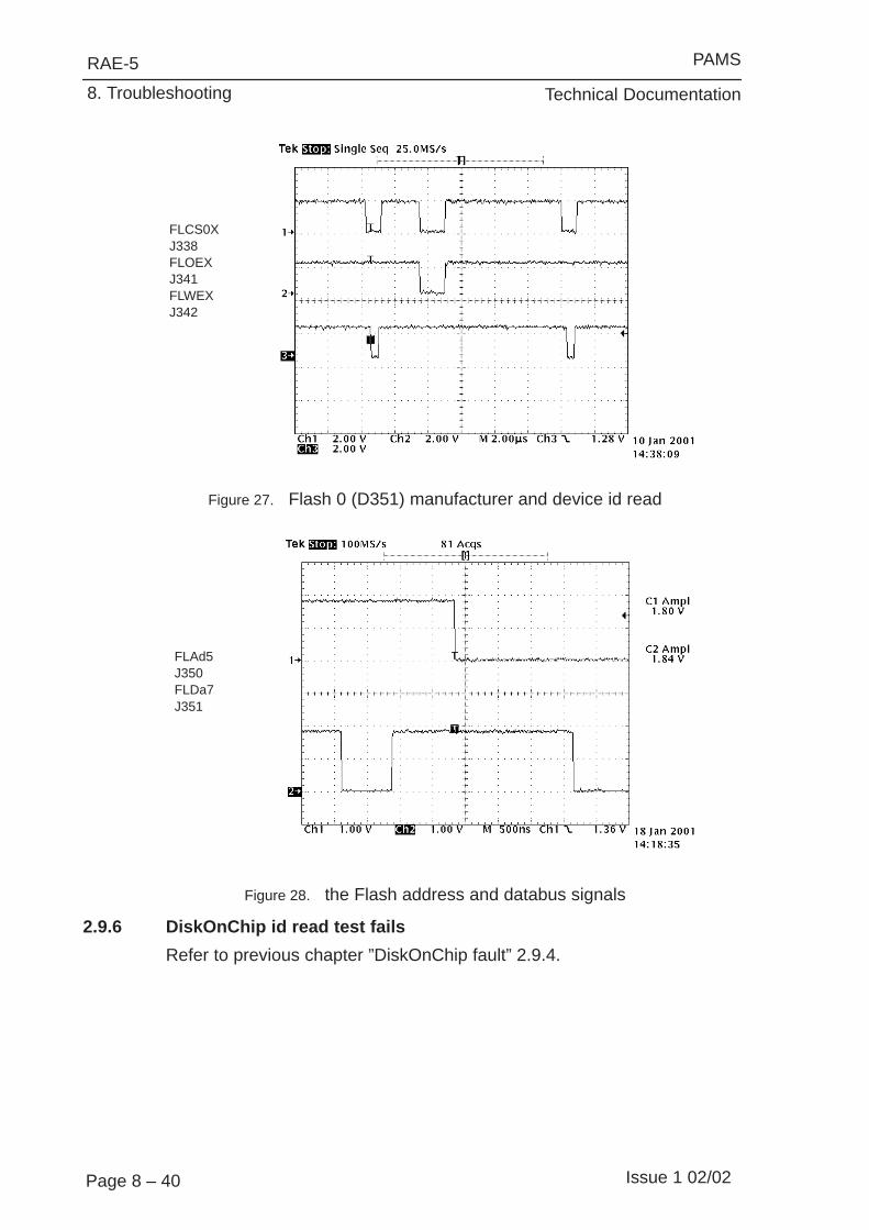
FLCS0XJ338FLOEXJ341FLWEXJ342
FLAd5J350FLDa7J351
PAMS
Technical Documentation
RAE-5
8. Troubleshooting
Page 8 – 40 Issue 1 02/02
Figure 27. Flash 0 (D351) manufacturer and device id read
Figure 28. the Flash address and databus signals
2.9.6 DiskOnChip id read test fails
Refer to previous chapter ”DiskOnChip fault” 2.9.4.

PAMS
Technical Documentation
RAE-5
8. Troubleshooting
Page 8 – 41Issue 1 02/02
2.10 Serial Interface Troubleshooting
2. Check and replace
1. Check Serial connector
4. Check DCE_Rx (AccTxData)
3. Check DCE_Tx (AccRxData)
Serial I/OOK
NO
Serial Interface problem
Flashingsuccessful?
X450 spring contacts
ESD protection device V451
comp. R452, C458, R300
comp. R450, C453, R309
Flashingsuccessful?
Check that ”DTR Detection”state changes by pressing
ACC_VOLTAGE switchin the service jig
Activate WinTesla,observe
ADC–readings
OK?
Check DCE_DTR linecomp. R454, C459,V489, R310
OK?
Refer to Accessory poweroutput troubleshooting
Faulty MAD (N300)or PWB fault
OK
YES NO
YES NO
NO
YES
5. Check DCE_DCD (MBus)
comp. R453, C457, R307
Figure 29.
NOTE1: Ensure that the customer’s DLR–2L is OK.
NOTE2: Wintesla ADC–readings for ’DTR Detection’: state ”0” = DCE_DTR– line at 2.8 – 3.0V
Wintesla ADC–readings for ’DTR Detection’: state ”1” = DCE_DTR– line at 0 – 0.3V
NOTE3: Signal levels in practice: High 2.7V, Low 0.3V
Exception: Diode in DTR line causes voltage drop, see Figure 30 below:

0.3V
2.95V
2.8V
With DLR–2LC1, black: MAD endC5, green: syscon end
PAMS
Technical Documentation
RAE-5
8. Troubleshooting
Page 8 – 42 Issue 1 02/02
0 V
Using DLR–2:GRP1, black: MAD endGRP2: System connector end
Figure 30. DTH line voltage

PAMS
Technical Documentation
RAE-5
8. Troubleshooting
Page 8 – 43Issue 1 02/02
MBUS (clock) Signal during flashing (Figure 31):
GRP1, black: MAD–endGRP2: system connector endApprox. 0.2V difference results from MBUSpull–up resistor (R309, 4k7) & serial resistor(R450, 270R) voltage slicing.
Figure 31. MBUS (clock) Signal during flashing

PAMS
Technical Documentation
RAE-5
8. Troubleshooting
Page 8 – 44 Issue 1 02/02
2.11 CONTACT SERVICE in CMT display
CONTACT SERVICE in CMT display (Self-tests with WinTesla)
Display Information: ”Contact Service”
This fault means that software is able to run and thus the watchdog of CCONT(N100) can be served. Self–test functions are executed when power is switchedon and software is started to execute from flash.
If any one of the self–tests fails (except no. 3, 7, 8, and F), the text ”ContactService” is shown in the phone display.
MCU Self–tests are divided into those executed while power up (tests: 1–5 and9–I ) and the ones can be executed with the connected PC. The tests and in-cluded items are as follows (Figure 32, screendump from the WinTesla)
Figure 32.
The information can be used for diagnosis.
Memory tests differ from normal DCT3 self–tests. They can not be executed inthe ENOS because memory protection.
There is no EEPROM. The EEPROM is emulated in the FLASH (part of CS2).All contents where EEPROM is mentioned refer to emulated EEPROM.
Item no. 1; MCU ROM Checksum:

PAMS
Technical Documentation
RAE-5
8. Troubleshooting
Page 8 – 45Issue 1 02/02
Calculates 16 bit checksum out of Flash code and compares it to the one foundin Flash. Items being checked are MADLinda <–> Flash data– and addresslines FLDa0–15 and FLAd1–21, FLCS0X (CE0), FLCS1X (CE1), FLCS2X(CE2), FLWEX (WE), Vbb (Vcc), VCORE (Vccq), GND, and Flash internal func-tionality.
Item no. 2 MCU EEPROM Interface:
Checks current PMM error status. If this test FAILs, the PMM data is not validanymore and should be formatted.
Item no. D COBBA Serial
This test tests Audio interface (PCM) of the COBBA_GJP.
Item no. E COBBA Parallel
This test tests the serial control/RF interface of the COBBA_GJP.

PAMS
Technical Documentation
RAE-5
8. Troubleshooting
Page 8 – 46 Issue 1 02/02
2.12 CCONT Serial interface Troubleshooting
If there are problems in CCONT’s serial control interface, self tests fail andthere is ”Contact service” shown on the display. Wintesla shows this fail as”CCONT Interface”.
NOTE: Low level means 0V, high level means approximately 2.8V.
Check GENSCLK line at J318Square wave, Freq. 2.17 MHz ?(see note below?)
Check CCONTCSX line at J317Activity?Signal active low
Check GENSDIO line at R308Activity?Signal active high
NOD300 or PWBOK?
YES
Check all three lines simultaneously, see fig. below
faulty
Figure 33.
(Note: Measurement should show 2.17MHz square wave. This interface is con-nected to CMT display also, so there is other activity too. The 3.1MHz clock istargeted for CMT display, do not worry about that. The clock signal is low wheninactive.)
1. Measure all the three lines simultaneously (Figure 34).
Set the trigger to CCONTCSX line falling edge.
You should see the two cases, Figure 34 and Figure 35 .(Channel 1–GENSClk, Channel 2–CCONTCSX, Channel 3–GENSDIO). High level is about 2.8V
Figure 34.

PAMS
Technical Documentation
RAE-5
8. Troubleshooting
Page 8 – 47Issue 1 02/02
MADLinda writes to CCONT. The data at sixth bit is ’0’ as marked with the cur-sors. The data after the read/write bit varies, just like the address before the bit.If you can see this kind of traffic, MADLinda side of the interface is functioningcorrectly.
Figure 35.
MADLinda reads from CCONT. The data at sixth bit is ’1’, marked with the cur-sors. There should be data seen after the ’read’ bit. All zero values may beread, but there should be other data seen, too. CCONT read cycles are fairlyrare compared to write cycles. If there is not any non–zero reads from CCONT,the CCONT (N100) may be faulty.

PAMS
Technical Documentation
RAE-5
8. Troubleshooting
Page 8 – 48 Issue 1 02/02
2.13 SIM Card
2.13.1 SIM Card Error Troubleshooting
The fault information ”SIM Card error” means most likely that the SIM lockedphone has been inserted with a SIM which does not correspond to the lockcode.
Check the SIM lock status of the phone with WinTesla:
NO
YESBlank
”SIM Card Error”message in display ?
Set the phone in NORMAL mode
View–> Quick/RF Info
See ”SIM Lock Settings” field:
field?No SIM lock.Refer to ”SIM Card Rejected”troubleshooting
SIM lock activated: inform customer
Customer contacts network operatorto ask for lock reset
Figure 36.

PAMS
Technical Documentation
RAE-5
8. Troubleshooting
Page 8 – 49Issue 1 02/02
2.13.2 SIM Card Rejected
The fault information ”SIM Card rejected” means that the ATR message (An-swer To Reset; the first message from SIM card to phone after SIM card powerup) is sent, but it is corrupted somehow, eg. the dataline signal levels are wrongor factory set values (stored in the EEPROM) are not correct.
NOTE1: CHECK THE MEASUREMENT POINT PICTURE BEFORE SERVICEACTIONS
SIM_xxx_Cardside – refers to signal which exists in SIM card contacts
SIM_xxx_o – refers to signal which exists in CCONT(N100) side
NOTE2: SIM Signals between CCONT (N100) and LindaMAD (D300) are notpossible to measure in KL8–module because traces are running in inner layersof PWB.

PAMS
Technical Documentation
RAE-5
8. Troubleshooting
Page 8 – 50 Issue 1 02/02
SIM CARD FAULT
Check VSIM at SIM card pin
VSIM=2,8V min. with 3V
4.5V min. with 5V
Check V103 pinsPin_1: CLK
Pin_6: DATAPin_4: Reset
Linesrising
0V –>3V/5Vafter power on
?
Check ATR data at N100
R112at N100 (CCCONT)side /SIM_DATA_0
3V card: CheckN100 (CCONT)C112, C113Replaceif necessary
CheckSIM card readermechanicalconnections
CheckX101, V103,R109, R112R125
5V card:Check5V charge pumpcomponentsC107V101C110
Stillproblem?
ReplaceN100
(CCONT)
CheckN100 (CCONT)
Stillproblem?
D300 (MAD) faulty N100 faulty
NO
YES
YES
YES
YES
NO
NO
NO
NO
YESOK?
YES
cardcard
and eventualshort circuits fromCLK, DATA andRESET linesagainst GND
Figure 37.
PAMS
Technical Documentation
RAE-5
8. Troubleshooting
Page 8 – 51Issue 1 02/02
2.13.3 Insert SIM card
The hardware of the SIM interface from the MADLinda (D300) to the SIM con-nector (X101) can be tested without SIM card. This leaves SIM connector(X101) contacts to be used as an measurement points.
When the power is switched on and if the BSI line (X100:2) is grounded by re-sistor (which happens automatically in service jig), all the used lines (VSIM,RST, CLK & DATA) rise up to 3V and/or 5V four times (SW tries to ask SIM cardfour times).
NOTE1: CHECK THE MEASUREMENT POINT PICTURE BEFORE SERVICEACTIONS
SIM_xxx_Cardside – refers to signal which exists in SIM card contacts
SIM_xxx_o – refers to signal which exists in CCONT(N100) side
NOTE2: SIM Signals between CCONT (N100) and LindaMAD (D300) are notpossible to measure in KL8–module because traces are running in inner layersof PWB.

PAMS
Technical Documentation
RAE-5
8. Troubleshooting
Page 8 – 52 Issue 1 02/02
Insert SIM card fault
Check Voltage level between R121 and C126
Check VSIM, DATA, RESET, CLOCK lines
Linesrising 0V–>3V/5V
after power on ?
Check VSIM (V103 pin 3)
3V card: CheckN100 (CCONT)C112, C113Replaceif necessary
Check SIM card,SIM card readermechanicalconnections
CheckX100, V103R109, R112R125
5V card:Check5V charge pumpcomponentsC107V101C110
Stillproblem?
FaultyN100
(CCONT)
ReplaceN100 (CCONT)
Stillproblem?Replace D300 (MAD)
NO– 3V
YES
YES
YES
NO–5V
NO
YES
When BSI resistor connected (included in service jig
Volt.level<1.5V ?
CheckNOR121, R122, X100, C126
YES
YES
at the pins of ASIM connector (X100)or SIM_xxx cardside signals at
measurement points
YES
YES
DATA_0 (R109)SIMRST_0 (R125) atN100/CCONT side
(ref. Measurement point diagram)
Linesrising 0V–>3V/5V
after power on ?
NO
YES
NO
NOStill
problem?
SIM I/O OK,N100 (CCONT)faulty
Faulty D300
Faulty PWB
VSIM at SIM card pin2.8V min. with 3V card
4.5V with 5V card
Figure 38.

PAMS
Technical Documentation
RAE-5
8. Troubleshooting
Page 8 – 53Issue 1 02/02
2.14 Memory Card
2.14.1 Memory Card Interface Troubleshooting
Start with assembled device with a faultless memory card inserted.
If necessary, proceed with tests in the jig with the faultless memory card in-serted.
Clk, Cmd and Data OK means that frequency, rise and fall timing are OK duringvarious operating modes.
Note:During initialization phase (MMCClk = lower frequency) the response viaMMCCmd line from card to MAD is sent in open drain mode i.e. rise time isabout 1us.Voltage of MMCCmd and MMCDa signals depends on direction of transfer(MAD I/O voltage is 2.8V and Card I/O is 3.0V).
Test pads J10x are located on the JL4 board of the Module Jig.
Troubleshooting diagram next page, Figure 39.

PAMS
Technical Documentation
RAE-5
8. Troubleshooting
Page 8 – 54 Issue 1 02/02
Test OK?
SwitchOK ?
RefMemory cardcover switch
fault tree
A faulty Memory Card used before ?SW corruption ?
Clk OK ?
Check X001/4Measure N103/1(control fromMAD while re–running thetest
Check X001/2R005, R002V001/3
Check X001/5R004 andV001/4
Check X001/7R001, R003and V001/6
Parts OK?
CtrlOK?
CheckN103C114C123
R007C001
Assembled device
Disassembled device in jig
Memory cardinterface check
YES
NO
YES
NO
OK?
C124
2.9 – 3.1V ?
NO
YES
NO
YES
YES
YES
YES YES
YES
YES
NO
NO
NO
CMD OK ?
Run WinTeslaMemory card
test
Run Memory Cardcover Switch
fault test
Measure VMMCJ104 while re–running
the MemCard test
Measure MMCClkJ105 while re–running
the test
Measure MMCCmdJ102 while
re–running the test
Measure MMCDa J107
Data OK?
Parts OK ? MAD I/OUndefined CPU error
MAD I/O
fault
fault
Figure 39.

PAMS
Technical Documentation
RAE-5
8. Troubleshooting
Page 8 – 55Issue 1 02/02
2.14.2 Memory card switch troubleshooting:
NOTE1: Memory card switch pressed (lid closed) => ADC reading ’MemoryCard Cover Detection’ is in state ”0” => MMC_Switch – line = 0V
Memory card switch released (lid opened) => ADC reading ’Memory Card Cov-er Detection’ is in state ”1” => MMC_Switch – line = 2.8V
Open WinTesla
MMC Close MMC card cover and
Open RAE3 lid after boot
Faultycircuit
D300 (MAD)or PWB
YES
YES
MMC Card cover switchproblem
Testing–>ADC Readings
lid openaccording toWinTesla ?
wait updated valuesfrom WinTesla
*
Lidclosed
according toWinTesla ?
*
Check J001(MMC switch)
OKCheck C002 and V001
OK?
Check mech.functionality
of J001check contact
surfaces
MMC coverswitch J001
OKOK?
MMC coverswitch J001
broken
NO
NO
OK
YESNO
CheckR006
OK?
R006faulty
* note:Cover opened MMC cover detection =”1”Cover closed MMC cover detection = ”0”
Figure 40.

PAMS
Technical Documentation
RAE-5
8. Troubleshooting
Page 8 – 56 Issue 1 02/02
2.15 Lid Switch
2.15.1 Lid Switch Troubleshooting
NOTE1:
Lid signal (MAD pin P2 gendet) :
Lid closed = ’Cover Detection’ from Wintesla ADC readings is state ”0”
=> V301 (HALL) output = 2.8V
Lid opened = ’Cover Detection’ from Wintesla ADC readings is state ”1”
=> V301 (HALL) output = 0V
Troubleshooting diagram Figure 41 next page.

PAMS
Technical Documentation
RAE-5
8. Troubleshooting
Page 8 – 57Issue 1 02/02
Turn the phone power onOpen the lid
Open Wintesla Select Testing –>ADC Readings
Wintesla:Lid Open OK
(coverdetection
state1) ?
Place magnet above the TAB key,note: pole toward the key !thenwait Refresh from Wintesla
N301pin 1
(Hall supply volt)2.8V ?
CheckV301, C322
Use serv.jigmagnet
Out–put toggle
of V301 pin 3low state(<0.3V)
?
Wintesla:Lid Closed OK(ADC reading
Coverswitch=
”0”
CheckV301,
(solders) R302If OK,
replace V301
Lid switch OK?Check/replacemagnetin the lid
CheckHall supply volt.
level at V301 pin 1(VBB) 2.8V
OK?
Use serv.jigmagnet
CheckV301, C322
Out–put toggle
of V301 pin 3high
?
FaultycircuitD300(MAD)
orFaulty PWB
CheckV301 solders
Shortcircuit inC323 ?
R302:high voltage level
(2.8V) at bothends?
Check trace betweenV301 pin3 and R302Replace V301
Lidswitch
trouble–shooting
OK
NO
YES
NOYES
YES
NO
NO
YES
YES
NO
YES
NO
NO
ASSEMBLED DEVICE
DEVICE IN JIG
Figure 41.

PAMS
Technical Documentation
RAE-5
8. Troubleshooting
Page 8 – 58 Issue 1 02/02
2.16 Battery Removal Switch troubleshooting
NOTE1: Switch itself is not possible to test in service jig.
NOTE2: Switch FREE position = Wintesla ADC–readings ’Battery RemovalSwitch’ is in state ”0” =>BATT_REM – line = 2.8V
Switch CONNECTED position = Wintesla ADC–readings ’Battery RemovalSwitch’ is in state ”1” => BATT_REM – line = 0V
NOTE3: Battery removal switch (latch spring) gets connected when batterylatch is pressed during battery release.
Refer to the diagram Figure 42 next page.

PAMS
Technical Documentation
RAE-5
8. Troubleshooting
Page 8 – 59Issue 1 02/02
Open WinTesla
Battery Keep latch in opposite position
Latch ”FREE” position
FaultycircuitD300(MAD)
YES
YES
Battery removal switchproblem
Testing–>PDC readings
removal switchstate =”0”
?
wait updated valuesfrom WinTesla
State
changes to
”1” ?
Battery removalswitch
Voltage
NO
OK
YESNO
Check B–to–B adapter
OK
Reading”1” though
latch position”FREE” ?
Short circuit inswitch lines
(BATT_REM)Check Z401
JC4 pin 42: BATT_REMline:
high (=2.8V)?
NOYES
YES NO
1. Check latch spring and AF8 pads
2. Check B–to–B connector X400 ofUL8 and flex FL13. Check filter Z401 BATT_REM line
Figure 42.

PAMS
Technical Documentation
RAE-5
8. Troubleshooting
Page 8 – 60 Issue 1 02/02
2.17 COBBA Control Interface troubleshooting
NOTE: If there are problems in COBBA serial interface, self tests fail and thereis ”Contact service” shown on the display. Wintesla shows fails at ”Cobba paral-lel”.
Check COBBACLK line at J322Square wave, Freq. 13MHz ?Signal rising/falling edge 3 to 5 ns?
Check COBBASDA line at J324Activity?
Check COBBACSX line at J323Activity?
NOD300 or PWBOK?
YES
Check all lines simultaneously, see fig. below
faulty
Signal duty cycle about 50per cent?Low when inactive?
Signal rising/falling edge 3 to 5 ns?High when inactive ?
Signal rising/falling edge 3 to 5 ns?High when inactive ?
Check COBBARSTX a J321High (about 2.8V) ?
Figure 43.
Figure 44. Write sequence to COBBA.
Figure 44 is a write sequence to COBBA. There should be non–all–zero writesto COBBA.

PAMS
Technical Documentation
RAE-5
8. Troubleshooting
Page 8 – 61Issue 1 02/02
Figure 45. COBBA read
Figure 45 is a COBBA read.
The MADLinda writes first the address to be read, deactivates the COBBACSXline and then activates the COBBACSX line again. Then the COBBA_GJPsends the requested data. There should be non–zero reads.
If no non–zero reads from COBBA can be seen, COBBA (N200) may be faulty.
If both reads and writes of non–zero values can be seen and the signal charac-teristics were good, the COBBA serial control interface is working correctly.

PAMS
Technical Documentation
RAE-5
8. Troubleshooting
Page 8 – 62 Issue 1 02/02
2.18 COBBA PCM Interface Troubleshooting
PCM interface transfers digital audio data. Problems in this interface result inmissing or flawed audio in either or both in uplink and downlink directions. IfWintesla shows errors in ”COBBA serial interface”, PCM interface is faulty.
Check PCMDClk signal at J309:520 kHz square wave50 per cent duty cycleRising and falling edges about 3 to 5 nsInactive state low?
NOYESOK? N200 faulty
Check PCMSClk at J306short pulse, rate 8.000kHz1.52 per cent duty cycleRise and fall times about 3 to 5 nsInactive state low?
NOYESOK? N200 faulty
Check PCMRx Data signal at J308Activity during call and voice recordingIf mic picks up sound, higher states at the cycle startRise and fall times about 3 to 5 nsSignal idle state High with some 13MHz noise?
NOYESOK? N200 faulty
Check PCMTx data signal at J307Activity during call Rise and fall times about 4 to 7 nsIdle statle low?
NOOK? N200 faulty
Ref. fig. 49
Ref. fig. 48
Ref. fig. 50
Ref. fig. 51
Figure 46.
There is no traffic in PCM interface without a call or audio play (voice recorder,video player, etc). These signals can be measured with a call, which generates

PAMS
Technical Documentation
RAE-5
8. Troubleshooting
Page 8 – 63Issue 1 02/02
traffic in both directions. Audio play generates traffic in one direction only. Re-cording audio (voice recorder) generates traffic in the other direction.
Figure 47. PCMDClk signal at J309
Figure 48. PCMSClk signal at J306.

PAMS
Technical Documentation
RAE-5
8. Troubleshooting
Page 8 – 64 Issue 1 02/02
Figure 49. PCMRxData signal at J308.
Figure 50. PCMTxData signal at J307
PCMTxData signal at J307 (Figure 50). This signal comes from the other end’smicrophone or audio playing software (voice recorder, video player etc) and istargeted for the earpiece or hands free speaker. There should be activity duringa call. Signal rise and fall times are around 4–7ns. Idle state is low.

PAMS
Technical Documentation
RAE-5
8. Troubleshooting
Page 8 – 65Issue 1 02/02
2.19 Audio troubleshooting
2.19.1 Both Mic and Earpiece/PHF faulty
MIC and Earpiece /PHF
Check voltage at cap C208
faulty
HOOKDET
HOOKDET
without external audio devices
2,8V?
Check voltage at cap C202HEADDET
without external audio devices
2,8V?
CheckR206 and R207,
Check frequency at J309
NO
CheckR203, R202, R200
PCMDClk during a call
520kHzFaulty
N200 (COBBA) *
OK
OK NO
square wave 2.8Vpp(ref.fig.53)
Check frequency at J306
PCMSClk during a call
8 kHzFaulty
N200 (COBBA) *square wave 2.8Vpp
(ref.fig.54)
NO
NO
OK
C208
C201,C202
HEADDET
* refer to section 2.17in this document
Figure 51. PCMDClk

PAMS
Technical Documentation
RAE-5
8. Troubleshooting
Page 8 – 66 Issue 1 02/02
Figure 52. PCDClk
Figure 53. PCMSClk

PAMS
Technical Documentation
RAE-5
8. Troubleshooting
Page 8 – 67Issue 1 02/02
2.19.2 Mic faulty
MICfaulty
Data
Check voltages :V202 pin 1 : 1.8V
Voltages
NOOK
OK NO
Voltages OK?
Check analog audio signal at
Signal a few mV ?
NO
NO
OK
OK?
V202 pin 3: 0.17Vduring a call
OK?
Mbias at R2222.1V during call?
DC voltage at C234 and C2351.4V during call ?
C232 during a call *
* *
Check R222, R218C231, C224,
C230
CheckC234, C235
Fault in N200 (COBBA)
NO
CheckC234, C235
CheckC225, C240, R219,
R220 and PWB traces
Check microphone and mic connections to PWBCheck digital PCM data atJ308 (PCMRxData)during a call
Faulty N200 (COBBA)Refer toCOBBA controlinterface troubleshooting
OK
OK
Figure 54.
Note:* can not be measured in the service jig, because components are underthe SIM connector.
Use wire to measure them. After removing measurement wire, check that com-ponents are not defected. It is recommended to replace the components.

PAMS
Technical Documentation
RAE-5
8. Troubleshooting
Page 8 – 68 Issue 1 02/02
2.19.3 Earpiece faulty
Earpiece
Check assembly of
faulty
Connection
Check digital PCM dataat J307 (PCMTxData)
Data
NOOK
OK NO
Voltages OK?
Check analog audio signal at
Signal a few mV ?
NO
NO
OK
OK?
during a call
OK?
DC voltage at C228, C2291.4V during call ?
C228, C229 during a call
earpiece and gasket
Check connections from audio PWB to C229 and C228
FaultyD300 (MAD) 2)
FaultyN200 (COBBA)
OK?
1)
Check R215, R216 andconnections.
CheckC228, C229
Check Flex UL8 andB–to–B conn X400
pins 47, 48
Figure 55.
Note:
1) If sound is distorted or too quiet fault is most probably in the gasket or in theearpiece diaphragm.
2) Refer to section 2.16 in this document.

PAMS
Technical Documentation
RAE-5
8. Troubleshooting
Page 8 – 69Issue 1 02/02
2.19.4 PHF Speaker faulty
PHF Spealer
Check assembly of HF speaker,
faulty
Connection
Check VAMP atR201, R204, R205, R221
VAMP
NOOK
OK NO
Voltages OK?
Amplifier enabled?
Voltage low?
NO
NO
OK
OK?
about VBATT ?
AMP SHDN at V200 pin 2
springs and connection to flex UL8
Check connections from speaker pads to C236 and C237
2.8 V during a PHF call ?
Faulty
V200
Check voltage at N201 pin 1
Faulty
D300 (MAD)
OK
Continues next page
Check R201, R204, R205,
Check Flex UL8 andB–to–B conn X400
pins 43 to 46
(Note: R201, R221 only in BL8_18)
C203, C204, C205, C206
Note:R204 and R205 havedifferent resistancevalues in BL8_17 and BL8_18
*
*
*
R221
Figure 56.

PAMS
Technical Documentation
RAE-5
8. Troubleshooting
Page 8 – 70 Issue 1 02/02
FaultyN200 (COBBA)
Check analog audio input signal
Signal amplified (ca. 10x)at N201 pins 5 and 8 ?
NO
NO
OK
FaultyN200 (COBBA)
NO
NO
OK
OK?
XEAR at C220, min. some 10 mV
Analog audio signal at C236 and C237?
OK?NOCheck
L200, L201,PWB connections
PHF speaker fault continued
CheckR208, C213 and XEAR traces from
C220 to N200
Check R212, R213, C220, C241, C223,
C217, C218
FaultyN201 (audio amp)
OK
Faulty
Figure 57.

PAMS
Technical Documentation
RAE-5
8. Troubleshooting
Page 8 – 71Issue 1 02/02
2.19.5 Headset out of order
Check XMIC and
AUXOUT
Voltage
OK
Check XEAR and GND lines
D300 (MAD)
OK?
NO
Headset out of order
NO
OK
RAE–3detects HS ?
(CMT lcd reads”headset”)
NOat C202 (HEADDET)
low ?
faulty SGND linesfrom System Conn.X450 pins 6 and 4
CheckC202, R203, L452C464. R460, L450,C462, R455, C460C461, C452, C450
OK
Head–set earpiece capsule
OK ?
NO
from System ConnX450 pins 5 and 11
to COBBA and R208, C213, L451,C451, C463, R459
Check N100(CCONT) EAD value
with WinTeslaAccessor _detection
D300 (MAD)faulty
NO
Check C201
N200 (COBBA) faulty
OK
Head–set Mic OK during
a call ?
OK
Check XMIC line fromSystem Conn X450 to N200
andC207, C216, C215, C219
Continues next page
Measurementsin Service Jig
voltage betweenR200 and R202 is
1.5V during call?
OK
N100 or
Figure 58.

PAMS
Technical Documentation
RAE-5
8. Troubleshooting
Page 8 – 72 Issue 1 02/02
Check
Check voltage at C208 while
Voltage
D300 (MAD)
Headset out of order, continues
NO
OK
Remote control
NOat C208 (HOOKDET)
low ?
faulty
OKHead–
set faulty
switchOK ?
HS switch button is pushed
R207 and C208
Measurementsin Service Jig
Figure 59.

PAMS
Technical Documentation
RAE-5
8. Troubleshooting
Page 8 – 73Issue 1 02/02
2.20 RF Interface
2.20.1 Phone doesn’t register to the network or doesn’t make a call
Phone does not register to the network or does not
make a call
C254 (VCOBBA)>2.7V ? Check N100 CCONT
C100 (Vref) = 1.5V ?
YES
NO
Check C100, R211NO
Check supply voltage during RX slot:C101 (VCP) >4.8VC133 (VRX) >2.7V
C135 (VSYN_1)>2.7VC134 (VSYN_2)>2.7V
During TX slot:C136 (VTX) >2.7V
N600 (VCHP) = 4.7V ?
SynthPwr (J319) = 1 (2.8V) ?VCXO_Pwr (J302) = 1 (2.8V) ?
Check CCONT N100
Check D300 MADLinda
OK
NO
Check synthesizer lines during RX slot:J502, J501/J505 SENA1
J501 (SCLK)J500 (SDATA)
= Pulses ”0” –> ”1” ?And
R800 (Reset) = ”1” ?
CheckReser at
N600 pin1 =”1”?
CheckN600C783C784C785N505
(Hagar)
YES
CheckR800C793D300
(MADLinda)
NO
Check D300 MADLinda
Check RF control lines during RX slot:R708 (RxC, N240)= 0 – 2.3VB max.R832 (AFC, VCXO)=0 – 1.2V typ.
Check N200 COBBA
Check analog data signals during RX slotR533 (RxIN, Cobba)=0 – 1.5V DCC532 (RxIP, Cobba)=0 – 1.5V DCReceived signal is biased to DC,
nominal amplitude=50mVpp, freq.=13MHz
If DC failure:Check N200 Cobba,
elseCheck RF part
Check RF control lines during TX slot:R792 (TxC, Cobba)=0 – 2.3V max.
J320(TxP) = ”0” –> ”1”(2.8V)
NO
NO
NO
NO If TxC failure:Check N200 Cobba,
If TxP failure,Check D300
Check analog data signals during TX slot:R541 (TxIN, Cobba)R541 (TxIP, Cobba)
R546 (TxQN, Cobba)R546 (TxQP, Cobba)
Transmitted signal is biased to DC,nom.ampl=300mVpp, freq.=64kHz
NOCheck N200 COBBA
R541, R546,C540, C541
YES
NO
YES
YES
YES
YES
YES
YES
YES
YES
Check RF part
Figure 60.

PAMS
Technical Documentation
RAE-5
8. Troubleshooting
Page 8 – 74 Issue 1 02/02
2.21 IR Interface Troubleshooting diagram
IR test OK?(Wintesla)
IrDA test OK
VBB (Vcc)OK?
(N050/6)
IRED_A(Vled)
OK?(N050/1)
C052 – C054 OK? R050, R052, R053,R054, C055, C050OK?
Replace IR module
CPU fault
IRDO (Txd)OK?
(N050/3)
IRDI (Rxd)OK ?
(N050/4)
IREN (Sd)OK ?
(N050/5)
CANNOT BE MEASURED IN THE JIG
IR Test OK?
(Wintesla)
NO
YES
NO
NO NO NO
YES YES
YES NO
IR CHECK
Figure 61.

PAMS
Technical Documentation
RAE-5
8. Troubleshooting
Page 8 – 75Issue 1 02/02
2.22 KL8 related Keyboard problems
There may be several types of problems with keyboard. Usually some of thekeys (CMT and PDA) are not working, or several key presses happen simulta-neously.
If CMT informs ”Please close cover”, see ”Lid switch problems” section.

PAMS
Technical Documentation
RAE-5
8. Troubleshooting
Page 8 – 76 Issue 1 02/02
NOYES
OK?
OK?NO
Check, replaceOK?
CSP filters Z401 to Z404
Check, replace
Problem with QWERTYkeypad _1
Put BL8 module in test jig, connect B–to–B adapter JC4.DO NOT connect the UI module or Flex, yetDO NOT switch power on.
Check the resistance of Row and Col signals to GND.1)Resistance > 1 MOhm ?
Z401 to Z404
DO NOT connect the UI module or Flex yet.Turn power on.
Check Col signals at pins:49, 62, 60, 59, 54, 55, 56, 61, 53, 51
Voltage around 2.8V ?
NO
if voltage = 0
Check Row signals at pins:50, 69, 67, 65, 64, 63, 57, 68, 58, 52
Voltage around 0 V ?
CSP filters Z401 to Z404
Check, replace
if voltage >0
YES
Eliminate short circuits if
YES
Continue at next diagram
Note 1) Pins 49–65 and66–69 against pin 70 (gnd).
Refer to table 6.
Figure 62.

PAMS
Technical Documentation
RAE-5
8. Troubleshooting
Page 8 – 77Issue 1 02/02
NOYES
OK?
Cycle the power, retryOK?
CSP filters Z401 to Z404
Check, replace
Problem with QWERTYkeypad _2
Connect ROW0 to COL0Measure the short circuit with oscilloscopeSignal rise and fall times between 80 to 120 ns,
Repeat for each ROW– COL pair.
Switch the power on, wait for rebootConnect Flex and UI module to the jig.
Push the faulty key, check the column signal.Signal rise/fall time 120 to 200 ns? (1)
NO
D300 faultyYES
constant activity?
If no activity or rise/fall times our of range
CSP filters Z401 to Z404check
OK?YES
Figure 63.
Table 1. Keyboard matrix (keys on UL2 module highlighted) – English keymatCol0 Col1 Col2 Col3 Col4 Col5 Col6 Col7 Col8 Col9
Row0 cmtSoft1
cmtUp
cmtSoft2
pdaSoft 3
pdaSoft 1
Space Info < / >
Row1 cmtSend
cmtDown
cmtEnd
pdaSoft 4
pdaSoft 2
Z Shift C B
Row2 cmt 1 cmt 2 cmt 3 cmtProfile
cmtPower
Chr N M , @
Row3 cmt 4 cmt 5 cmt 6 cmt * cmt # Menu Up Right Down LeftRow4 cmt 7 cmt 8 cmt 9 cmt 0 :; +– Back-
spaceEnter
Row5 ESC App1 App2 App3 app4 App6 App7 App8Row6 Ctrl V X 6 App5Row7 1 2 3 4 5 7 8 9 0 PRow8 Tab Q W E R T Y U I ORow9 Caps A S D F G H J K L

PAMS
Technical Documentation
RAE-5
8. Troubleshooting
Page 8 – 78 Issue 1 02/02
Table 2. Keyboard line filters
Z402 Z403 Z404
Col4 Col1 Row1
Col5 Col2 Row2
Col6 Col3 Row3
Col8 Col7 Row4
Col9 Row5 Row7
Row9 Row6
Row8

PAMS
Technical Documentation
RAE-5
8. Troubleshooting
Page 8 – 79Issue 1 02/02
2.23 KL8 related PDA UI problems
NOYES
OK?
OK?
CSP filters Z401 to Z404
Check, replace
Problem with BL8
Put BL8 module in test jig, connect B–to–B adapter JC4.DO NOT connect the UI module or Flex yet.DO NOT switch power on.
Check the resistances of display signals to the GND (1)
Resistance > 1 MOhm ?
Turn the power on.Connect the Flex and the UI module.
Check LCDDA0 to LCDDA11 signals at JC4 pin header.Pins nos.5, 7, 19, 20, 22, 23, 24, 26, 36, 37, 38, 39
Constant activity, signal as in Fig 73?
NO
if voltage = 0
Check DispClk signal at pin 2. , use a min 1MOhm probeSignal as in Fig, 77?
YES
CSP filters Z401 to Z404
Check, replace
if voltage < 1MOhm
Check LLCLK signal at pin 40. Signal as in Fig, 78?
Check FSP signal at pin 4.Signal as in Fig, 79?
Check BackPWM signal at pin 31.Signal as in Fig, 80?
Check LCDPWM signal at pin 10.Signal as in Fig, 81?
CSP filters Z401 to Z404
Check, replace
OK?
YES
D300 or PWB faulty
Figure 64.

PAMS
Technical Documentation
RAE-5
8. Troubleshooting
Page 8 – 80 Issue 1 02/02
Figure 65. LCDDA0–LCDDA11 signals on the pin header on JC4. The pins are 5, 7, 19, 20, 22–24, 26, 36–39.
Figure 66. DispClk signal at pin 2
DispClk signal (Figure 66) at pin 2. Use at least 1MΩ probe for this.Note: The more critical values are high 1.8V, frequency 8.645MHz and +Width42ns. If the signal high time is too small, it will cause errors.

PAMS
Technical Documentation
RAE-5
8. Troubleshooting
Page 8 – 81Issue 1 02/02
Figure 67. LLCLK signal at pin 40.
Figure 68. FSP signal at pin 4.

PAMS
Technical Documentation
RAE-5
8. Troubleshooting
Page 8 – 82 Issue 1 02/02
Figure 69. BackPWM signal at pin 31
This signal (Figure 69) is a PWM control for display backlight. The pulse widthvaries and is constant high for maximum intensity.
Figure 70. LCDPWM signal at pin 10.
This signal (Figure 70) is a PWM control for display contrast. The pulse widthmay vary significantly.
Table 3: List of display signals
Table 3. List of display signals
Display Signal JC4 pin no. Display Signal JC4 pin no.
LCDDa0 5 LCDDa10 39
LCDDa1 26 LCDDa11 7
LCDDa2 24 DispClk 2
LCDDa3 38 LLClk 40
LCDDa4 20 FSP 4
LCDDa5 36 DISPON 3

PAMS
Technical Documentation
RAE-5
8. Troubleshooting
Page 8 – 83Issue 1 02/02
Table 3. (continued) List of display signals
JC4 pin no.Display SignalJC4 pin no.Display Signal
LCDDa6 37 LCDM 18
LCDDa7 22 LCD_PWR 6
LCDDa8 19 LCDPWM 10
LCDDa9 23 BackPWM 31
Table 4. CSP filters and PDA UI signals
Z400 Z401 Z402 Z403 Z404
DispClk LCDDa11 LCDM LCDDa1 BackPWM
LCDDa5 LCDPWM LCDDa8 LCDDa2
DISPON LCDDa4 LCDDa9
LCDDa6 LCDDa7
FSP
LCDDa3
LCDDa0
LCDDa10
LCD_PWR
LLClk

PAMS
Technical Documentation
RAE-5
8. Troubleshooting
Page 8 – 84 Issue 1 02/02
2.24 KL8 related CMT UI problems
NOYES
OK?
OK?
CSP filter Z401
Check, replace
Problem with CMT UI
Put BL8 module in test jig, connect B–to–B adapter JC4.DO NOT connect the UI module or Flex yet.DO NOT switch power on.
Check the resistances of display signals to the GND (1)Resistance > 1 MOhm, GENSDIO = 47kOhm?
Turn the power on.Connect the Flex and the UI module.
Check GENSCLK, signal as in Fig. 80 ?
NO
if voltage = 0
YES
CSP filter Z401Check, replace
Check GENSDIO siglnal while LCDEN is active.Rise/fall time: 30 to 60 ns?
Check LCDEN signal.
Check LCDRSTX signalSignal 2.8 V or active?
CSP filter Z401
Check, replace
OK?
YES
D300 or PWB faulty
NO
Rise/fall time: 30 to 60 ns?
Figure 71.

PAMS
Technical Documentation
RAE-5
8. Troubleshooting
Page 8 – 85Issue 1 02/02
Figure 72. GENSCLK signal.
GENSCLK signal (Figure 72 ). It should look like this when LCDEN signal is ac-tive. There is also a 2.16MHz clock signal, but it is targeted for CCONT.
Table 5. Signals and pins
Signal Pin no.
LCDEN 12
GENSDIO 9
GENSCLK 11
LCDRSTX 14
Table above: Signals and corresponding pins.

PAMS
Technical Documentation
RAE-5
8. Troubleshooting
Page 8 – 86 Issue 1 02/02
3 DL1 UI Troubleshooting
3.1 CMT and keypad illumination problems
Each CMT–display and keypad LED has its own driver. If there is problems withone or more
– Keypad–LED: check resistors R203–R208, transistors V213, V203, V204 andthe LEDs.
– CMT–LED: check resistors R200–R202, transistor V206 and the LEDs.
If the illumination does not work at all, measure voltages VB and KBLIGHTS.VB should be the same as VBATT and KBLIGHTS approximately 2.5V whenthe LEDs are supposed to be on. If these voltages are not correct, problem is inhinge flex, connector X001 or on KL8 (see 2.23 in this document).
3.2 CMT LCD Troubleshooting
CMT LCD
Check
faulty
Display
CMT LCD or LCD Flex
Display
YESNO
YESNO
OK?
OK?END
Problem in
C002, R003, X007Make sure that the display flex is
connected to X007
probably damagedReplace LCD.
Hinge Flex, connector X001or BL8
Refer to chapter2.23
Figure 73.

PAMS
Technical Documentation
RAE-5
8. Troubleshooting
Page 8 – 87Issue 1 02/02
3.3 No picture on PDA LCD or picture is faulty
To start with, check that the flex connector (X001) from KL8 to UL2 is con-nected properly and that soldering joints are ok.
Check also connectors X002 and X003. Check that PDA display is not mechan-ically damaged, i.e. pixels missing.

PAMS
Technical Documentation
RAE-5
8. Troubleshooting
Page 8 – 88 Issue 1 02/02
Picture onLCD?
Check testpatterns
withWInTesla
OK?
LCD OK!
NO
MeasureV5Y_1,
should beappr.–15V
NO V5Y_1 0V? YES
ON
MeasureST_INVOUT
(Fig.79)YES
Check componentsL050, C068, V062
and V069
ON
MeasureDD_P1(Fig.80)
YESCheck
components C058and R075
Display ASICfault(D054)
ON
MeasureBRIGHT(Fig.81)
NOSee Section: bl8related PDA UI
problems
YES
MeasureSET, should
be 1.4VOK?
NOCheck
componentsR063 and R070
YES
MeasureCONT,
should be400mV
CheckcomponentsR068, R072,
R077 and V056NO
MeasureTEMP,
should be850mV
YESCheck
componentsV055 and V058
NO
MeasureFB, shouldbe 900mV
OK?
YES
CheckcomponentsR066, V061,R067, R076,
V066, R078 andR081
NO
See Section 2
YES
YES
See Section 3
NO
YES
Start Section 1
Figure 74.
OK?OK?
OK?
OK?OK?
YES

PAMS
Technical Documentation
RAE-5
8. Troubleshooting
Page 8 – 89Issue 1 02/02
MeasureV5Y(Fig.85)
and VCCY(Fig.86)
YES
NO MeasureFRYS(Fig.84)
OK?
Display ASICfault
Checkcomponents
between FRYS,V5Y and VCCY
YES
MeasureVOY(Fig.85)
OK?
NOMeasureVDD, it
should be~3.8VOK?
NOMeasureDD_P2
(Fig.86)
Checkcomponents
V060, R079 andC064
YES
NO
YES
CheckcomponentsC076,V072,
N050, C075 andC101
Display ASICfault
Measure
DY(Fig.90)
FRY(Fig.91)
YSCL(Fig.92)
XINH(Fig.93)
YES
DY OK?
NO
YES
MeasureDY_A
(Fig.91) andXSET(should
be 2.8V)OK?
NO Display ASICfault
Checkcomponents
V050,R051,R050, V052,
R053,D050,V051R055
YES
FRY, YSCL,XINH OK? NO
YES
MeasureFRY_A (fig.92)YSCL_A (fig.93)
XINH_A(2.8V) OK?
NO
Checkcomponents
C051,R054,R052,
Display ASICfault
YES
MeasureXSCL
(Fig.94)OK?
YESNO Display ASIC
faultSee section 4
Start Section 2
OK?
OK?
and
D050, C052, D051D052, R056, V053V054, C054, C055R059, R064, R058, R061
Figure 75.
NO

PAMS
Technical Documentation
RAE-5
8. Troubleshooting
Page 8 – 90 Issue 1 02/02
NOTE!! See section 2.23. There are all the relevant pictures of the signalsmentioned below. Measure these signals from UL2 side. This is to make surethat the problem is not in KL8 side.
MeasureDispClk(J012),
OK?
YES
See section bl8 relatedPDA UI problems
MeasureLLClk(J027),
OK?
MeasureFSP(J020),
OK?
YES
MeasureDISPON(J021),
2.8V?
YES
MeasureLCDDA0–A2,A4,A7–
A9,A11(J019,J002,J004,J007,J006,J008,J005,J017),
OK?
YES
NO
NO
Return to section1YES
Start Section 3
Figure 76.

PAMS
Technical Documentation
RAE-5
8. Troubleshooting
Page 8 – 91Issue 1 02/02
MeasureD10,D11,D12 and
D13(Fig.98)OK?
YES
NO Checkcomponent R087
Signals OK? DisplayASIC(D054) faultNO
MeasureD00,D01,D02 and
D03(Fig.98)OK?
YES
MeasureD20,D21,D22 and
D23(Fig.98)OK?
Checkcomponent R088NO
NO Checkcomponent R090
MeasureRES,LP and
GOP(Figs.99, 100,
101 )OK?
YES
Checkcomponent R089NO
Measure FR(Fig.102)
OK?
YES
Checkcomponent R091NO
Display module faultYES
YES
Start Section 4
Figure 77.

PAMS
Technical Documentation
RAE-5
8. Troubleshooting
Page 8 – 92 Issue 1 02/02
Figure 78. ST_INVOUT signal
Figure 79. DD_P1 signal
Figure 80. BRIGHT signal

PAMS
Technical Documentation
RAE-5
8. Troubleshooting
Page 8 – 93Issue 1 02/02
Figure 81. V5Y signal
Figure 82. VCCY signal
Figure 83. FRYS signal

PAMS
Technical Documentation
RAE-5
8. Troubleshooting
Page 8 – 94 Issue 1 02/02
Figure 84. VOY signal
Figure 85. DD_P2 signal
Figure 86. DY signal

PAMS
Technical Documentation
RAE-5
8. Troubleshooting
Page 8 – 95Issue 1 02/02
Figure 87. FRY signal
Figure 88. YSCL signal
Figure 89. XINH signal

PAMS
Technical Documentation
RAE-5
8. Troubleshooting
Page 8 – 96 Issue 1 02/02
Figure 90. DY_A signal
Figure 91. FRY_A
Figure 92. YSCL_A signal

PAMS
Technical Documentation
RAE-5
8. Troubleshooting
Page 8 – 97Issue 1 02/02
Figure 93. XSCL signal
Figure 94. Data signal
(Note!! There should be constant activity in the datalines and signals shouldlook something like this.)

PAMS
Technical Documentation
RAE-5
8. Troubleshooting
Page 8 – 98 Issue 1 02/02
Figure 95. RES signal
Figure 96. GOP signal

PAMS
Technical Documentation
RAE-5
8. Troubleshooting
Page 8 – 99Issue 1 02/02
Figure 97. LP signal
Figure 98. FR signal

PAMS
Technical Documentation
RAE-5
8. Troubleshooting
Page 8 – 100 Issue 1 02/02
3.4 Backlight troubleshooting
LCD_PWR signal HIGH
PDA backlight
dark / dim
Check
R155, X001
BACKPWM signal HIGH or
335 Hz square wave *
Check
X001, R156,
C160, V160
NO
NO
YES
YES
Check LED assembly, X006
connector
OKChange UL1_0x
module
NO

PAMS
Technical Documentation
RAE-5
8. Troubleshooting
Page 8 – 101Issue 1 02/02
BACKPWM signal HIGH or
335 Hz square wave *
Brightnesscontrol doesn’t
work
Check
X001, R156,
C160, V160
PDALEDS voltage
>= 14 V
(overvoltage protection limit)
Change UL1_0x
module
NO
NO
YES
YES
Check LED assembly, X006
connector
OKChange UL1_0x
module
NO
* Note! BACKPWM signal HIGH when maximum
brightness level setting.

PAMS
Technical Documentation
RAE-5
8. Troubleshooting
Page 8 – 102 Issue 1 02/02
3.5 DL1 related keyboard problems
1. Check the 50–way connector solderings and general condition
2. Check PDA softkey switches S250, S251, S260, S261
3. Check keyboard line capacitors C250–C263 (14 pieces) for shortsand breakages
4. Check the key pads for short circuits or dirt. Measure the resistanceof each row against all columns and all rows and columns against ground. (Dis-connect the 50–way connector first). Result should be > 1Mohm for all com-binations.

PAMS
Technical Documentation
RAE-5
8. Troubleshooting
Page 8 – 103Issue 1 02/02
4 UL 8 FLEX related
4.1 Audio troubleshooting
NO
Handsfree or/and Earpiece
Checksoldering of 70 way
connector
YES
Check solderingof AF8 PWB
OK?
CheckHF speaker
OK?NO
Replace part
connector
ResolderOK?
connector
Resolder
Audio not working
gold pads
NOYES
Figure 99.
AF 8 illustrated below (Figure 100).
Figure 100. AF8

PAMS
Technical Documentation
RAE-5
8. Troubleshooting
Page 8 – 104 Issue 1 02/02
4.2 Display problem
PDA or CMT displays are missing lines or columns, or are not synchronised
NO
Checksolderinf of 70 way
connector
YES
Check soldering of 50 way connector
OK?
Check
hinge tracks
for wear
OK?NO
Replace part
connector
ResolderOK?
connector
Resolder
Corruption of PDA or CMTLCDs
Figure 101.

PAMS
Technical Documentation
RAE-5
8. Troubleshooting
Page 8 – 105Issue 1 02/02
4.3 Battery Removal Switch problem
If the battery removal switch is not functional, check AF 8 for wear, illustratedbelow. (Check that the RAE-3 software supports the battery removal switch fea-ture.)
Figure 102. AF8
4.4 UL8 related keyboard problems
1. Check the 70–way and 50–way connector solderings and generalcondition. Re–solder if fault found.
2. Check the keypad surface for short circuits or dirt.
3. Replace the flex.

PAMS
Technical Documentation
RAE-5
8. Troubleshooting
Page 8 – 106 Issue 1 02/02
5 RF related troubleshooting
Introduction to RF troubleshooting
Measurements must be done using Spectrum Analyzer with high–frequencyhigh–impedance passive probe (LO–/reference frequencies and RF–powerlevels) and Oscilloscope with a 10:1 probe (DC–voltages and low frequencysignals).
The RF–section is build around one ASICS Hagar (N505). For easier trouble-shooting, this RF troubleshooting document is divided into sections.
Before changing Hagar, please check the following things: Supply voltages areOK and serial communication are coming to Hagar.
Please note that the grounding of the PA–module is directly below PA–moduleso it is difficult to check or change. Most RF semiconductors are static dis-charge sensitive! So ESD protection must be taken during repair (groundstraps and ESD soldering irons). Hagar are moisture sensitive so parts must bepre–baked prior to soldering.
Apart from key–components described in this document here are a lot of dis-crete components (resistors, inductors and capacitors) which troubleshooting isdone by checking if soldering of the component is done properly, for factory re-pairs (checking if it is missing from PWB). Capacitors can be checked for short-ening and resistors for value by means of an ohmmeter, but be aware in–circuitmeasurements should be evaluated carefully.
Please be aware that all measured voltages or RF levels in this documentare rough figures. Especially RF levels varies due to different measuringequipment or different grounding of the used probe.
5. RF related :
5.1 EGSM receiver
5.2 PCN receiver
5.3 EGSM transmitter
5.4 PCN transmitter
5.5 Synthesizer
5.6 Frequency lists

PAMS
Technical Documentation
RAE-5
8. Troubleshooting
Page 8 – 107Issue 1 02/02
RF Key Component Placement
Figure 103. Parts placement 1
Figure 104. Parts placement 2

PAMS
Technical Documentation
RAE-5
8. Troubleshooting
Page 8 – 108 Issue 1 02/02
5.1 EGSM Receiver
General Instructions for troubleshooting for EGSM RX
Select Product Alt+p
Open…. . . . . . . .
RAE–5
Select: Product Alt+p
Band b
EGSM e
Select: Testing Alt+e
RF Controls r
RX Continuous Alt+r
Cont. Mode Ch: 60 Alt+o, 60
AGC Absolute: 8
Multislot on Alt+u, (if on remove checkmark)
Apply
The set–up should now look like this (Figure 105):
Figure 105.
Apply a 947.06771MHz (channel 60 + 67.710kHz offset) –95 dBm signal to theRF–connector (remember to compensate for cable attenuation).

PAMS
Technical Documentation
RAE-5
8. Troubleshooting
Page 8 – 109Issue 1 02/02
Measuring with an oscilloscope on “Hagar RXI” or “Hagar RXQ” this pictureshould be seen from a working EGSM receiver:
Figure 106.
Signal amplitude 390mV p–p
DC offset 1,1V
Frequency 67kHz
If this picture is not seen, continue to the next section.
5.1.1 Troubleshooting diagram for EGSM Receiver
Apply –95dBm947.06771 MHz signal from
generator to antennaconnector
Oscilloscope at RXISignal 390mV p–pDC offset 1,1V *
Frequency 67,7kHz
EGSM chain functional
OscilloscopeVRX 2.7V
Check Hagar serialinterface
Yes
Yes
Yes
Spectrum analyzer LNA out C610
RFout –43dBm ?No No
Spectrumanalyzer1st EGSM SAW
out Z620 –58 dBm at C615?
GSM_RX–84dBm
No
SpectrumanalyzerT600, unbal
–45 dBm ?
CheckZ600. T600
No
Yes
Check HagarN505
Yes
Check BBNo
OscilloscopeLNA_G 2.4–2.8V
VLNA = 2.7V ?
Yes
Check RX/TXSwitchZ900
No
Check Z700
Yes
EGSM Fault tree
No
OscilloscopeR610 1.9VR611 0.9v ?
Yes
OscilloscopeVRX 2.7V
Check Hagar serial interface
Check HagarN505
Yes
Check BaseBandNo
CheckR706, R708,
V700,C701,C705,C718
No
CheckV904
Yes
Change generatorlevel to –50 dBm
Yes
Figure 107.
*If DC–offset is missing,check COBBA powering andsolders
Note: RF levels measured with HP85024A RF probe.

PAMS
Technical Documentation
RAE-5
8. Troubleshooting
Page 8 – 110 Issue 1 02/02
5.1.2 EGSM Signal PathFor easy error tracing it is important to know the signal path of the EGSM re-ceiver. The components can be grouped into blocks and drawn as shown below(Figure 108) .
22 2 2
INP_P_RX
INM_P_RX
RX
/TX
Sw
itch
RX
RX
TX
TXINP_G_RX
INM_G_RX
DNC2
DNC2
LNA_P
RXQ
RXI
OU
T_B
B1_I
OU
T_B
B1_Q
I_DC
N2_I
I_DC
N2_Q
C1_B
B1_I
C2_B
B1_I
C2_B
B1_Q
C1_B
B1_Q
Cp_f_I
Cm
_f_IC
p_f_Q
Cm
_f_Q
Cp_dtos_I
Cm
_dtos_I
Cp_dtos_Q
Cm
_dtos_Q
0–40dB
BB_Gain
0–40dB
BB_Gain
DtoS
DtoS
BIQUAD
BIQUAD
GSM
PCN
VR
F_R
X
VREF_RX
VB
_EX
T
RB
_EX
T
RFControls
LNA_G
8 / 18 dB
8 / 18 dB
SAW
SAW SAW
SAWLNA
LNA
Hagar
VRF_RX
VREF_RX
VREF
RXI
RXQ
LNAB_G
Antenna connector
Figure 108.
5.1.3 RX/TX SwitchFrom the internal antenna connector (X499) the RF signal is lead to the RX/TX switch (Z670) via a mechanical switch, the antenna connector (X450).
The RX/TX switch is normally routing the signal to the two RX outlets GSM_Rxand DCS_Rx. If no control voltage is present at VC1 or VC2 the RX/TX switchwill work as a diplexer and EGSM signals pass to GSM_Rx and PCN signals toDCS_Rx.
From GSM_Rx the EGSM signal is feed to the 1st EGSM SAW filter via C614.
5.1.4 Front endThe EGSM front–end consists mainly of two SAW filters (Z620 and Z600) andone discrete LNA circuit (V904) in–between and finally one balun (T600). TheSAW filters provides out–of–band blocking immunity, the LNA provides front–end gain and the balun provides a balanced signal for Hagar (N505)
The signal–path is through Z620 (In–band insertion–loss 3,5dB), through thematching circuit (C613, Z612, Z613) and to the EGSM LNA transistor base(V700, RFin).
The LNA has about 20dB gain when it is on (LNA_G = 2.5V and Vlna=2.8V). Ifthe signal applied to the antenna–connector is more than –45dBm the AGC willgainstep the LNA (LNA_G = 0V) which means the LNA Gain will now havenegative gain (loss).
From the LNA transistor collector (V904 RF out) the signal is lead through theLNA–output–matching–circuit (R610, Z615, C610), through the 2nd EGSMSAW Z600 (In–band insertion–loss 3,5dB) to the EGSM balun T700. From thebalun the signal is balanced and is lead to Hagar (N500 IMP_GSM_RX andINM_GSM_RX).

PAMS
Technical Documentation
RAE-5
8. Troubleshooting
Page 8 – 111Issue 1 02/02
5.1.5 Hagar
The balanced RX signal is mixed with a signal from the local oscillator at thesame frequency as the wanted RX signal. After mixing the signal is convertedto a singleended signal in the DtoS (Differential to Singleended) amplifier. Thesignal is now filtered in a BIQUAD filter to provide channelseparation, amplifiedin the BB_Gain amplifier and DC compensated in DCN2.

PAMS
Technical Documentation
RAE-5
8. Troubleshooting
Page 8 – 112 Issue 1 02/02
5.2 PCN Receiver
General Instructions for troubleshooting for PCN RX
Connect the phone to a PC with a DAU–9P cable
Start Wintesla–Service–Software and
Select Product Alt+p
Open…RAE–5
Select: Product Alt+p
Band b
PCN p
Select: Testing Alt+e
RF Controls r
RX Continuous Alt+r
Cont. Mode Ch:700 Alt+o, 700
AGC Absolute: 8. . . .
Multislot on Alt+u, if on remove checkmark
The set–up should now look like this (Figure 109):
Figure 109.
Apply a 1842.867 MHz (channel 700 + 67.710kHz offset) –95dBm signal to theRF–connector (remember to compensate for cable attenuation).
Measuring with an oscilloscope on “Hagar RXI” or “Hagar RXQ” this pictureshould be seen on a working PCN receiver:

PAMS
Technical Documentation
RAE-5
8. Troubleshooting
Page 8 – 113Issue 1 02/02
Figure 110.
Signal amplitude 350 mV p–p
DC offset 1,1V
Frequency 67kHz
If this picture is not seen, continue to the next section.
Apply –95 dBm1842.867MHz signal
from generator toantenna connector
Oscilloscope at RXISignal 350mV p–pDC offset 1,1V *
Frequency 67,7kHz ?
EGSM chain functional
OscilloscopeVRX 2.7V
Check Hagar serialinterface
Yes
Yes
Yes
SpectrumanalyzerLNA out L646,
–39 dBm?
No NoSpectrumanalyzer1st PCN SAW out at Z620
–56 dBm at C647 ?
PCN_RX–
No
SpectrumanalyzerT630, unbal–43 dBm ?
CheckNo
Yes
Check HagarN505
Yes
Check BBNo
OscilloscopeLNA_P 2.4–2.8V
VLNA = 2,7V ?
Yes
Check RX/TXSwitchz670
No
Check Z620
Yes
PCN Fault tree
No
Oscilloscope2.0V at R640 ?1.9V at R645 ?
Yes
OscilloscopeVRX 2.7V
Check Hagar serial interface
Check HagarN500
Yes
Check BaseBandNo
CheckV903
No
CheckV701
Yes
Change generatorlevel to –50 dBm
Yes
RF out
Z600, T630
V905R614R640R643R645C647C644C640C648C643C646L633L646L647
–56dBm atC645 ?
Figure 111.
*If DC–offset is missing,check COBBA powering andsolders

PAMS
Technical Documentation
RAE-5
8. Troubleshooting
Page 8 – 114 Issue 1 02/02
5.2.1 PCN Signal PathFor easy error tracing it is important to know the signal path of the PCN receiv-er. The components can be grouped into blocks and drawn as shown below.
22 2 2
INP_P_RX
INM_P_RX
RX
/TX
Sw
itch
RX
RX
TX
TXINP_G_RX
INM_G_RX
DNC2
DNC2
LNA_P
RXQ
RXI
OU
T_B
B1_I
OU
T_B
B1_Q
I_DC
N2_I
I_DC
N2_Q
C1_B
B1_I
C2_B
B1_I
C2_B
B1_Q
C1_B
B1_Q
Cp_f_I
Cm
_f_IC
p_f_Q
Cm
_f_Q
Cp_dtos_I
Cm
_dtos_I
Cp_dtos_Q
Cm
_dtos_Q0–40dB
BB_Gain
0–40dB
BB_Gain
DtoS
DtoS
BIQUAD
BIQUAD
GSM
PCN
VR
F_R
X
VREF_RX
VB
_EX
T
RB
_EX
T
RFControls
LNA_G
8 / 18 dB
8 / 18 dB
SAW
SAW SAW
SAWLNA
LNA
Hagar
VRF_RX
VREF_RX
VREF
RXI
RXQ
LNAB_G
Antenna connector
Figure 112. PCN RX signal path
5.2.2 RX/TX SwitchFrom the internal antenna connector (X499) the RF signal is lead to the RX/TXswitch (Z670) via a mechanical switch, the antenna connector (X900).
The RX/TX switch is normally open to the two RX outlets GSM_Rx andDCS_Rx. If no control voltage is present at VC1 or VC2 the RX/TX switch willwork as a diplexer and PCN signals pass to DCS_Rx and EGSM signals toGSM_Rx.
From DCS_Rx the PCN signal is feed to the 1st PCN SAW filter via C645.
5.2.3 Front endThe PCN front–end consists mainly of two SAW filters (Z620 and Z600) andone discrete LNA (V903) in–between and finally one balun (T630). The SAWfilters provides out–of–band blocking immunity, the LNA provides front–endgain and the balun provides a balanced signal for Hagar (N505)
The signal–path is Through Z620 (In–band insertion–loss max 4dB), throughthe matching circuit (C674, C644, L647) and to the PCN LNA (V903, RFin).
The LNA has about 18 dB gain when it is on (LNA_P = 2.8V and Vlna=2.8V). Ifthe signal applied to the antenna–connector is more than –45dBm the AGC willgainstep the LNA (LNA_P = 0V) which means the LNA Gain will now havenegative gain (loss).
From the LNA transistor collector (V904 RF out) the signal is lead through theLNA–output–matching–circuit (R640, L633, C640, L646), through the 2nd PCNSAW Z600 (In–band insertion–loss max 4dB) through a matching–network(C720 and L706) and to the PCN balun T630. From the balun the signal is bal-anced and is lead to Hagar (N505 IMP_PCN_RX and INM_PCN_RX).
5.2.4 HagarThe balanced RX signal is mixed with a signal from the local oscillator at thesame frequency as the wanted RX signal. After mixing the signal is converted

PAMS
Technical Documentation
RAE-5
8. Troubleshooting
Page 8 – 115Issue 1 02/02
to a single ended signal in the DtoS (Differential to Single ended) amplifier. Thesignal is now filtered in a BIQUAD filter to provide channel separation, amplifiedin the BB_Gain amplifier and DC compensated in DCN2.

PAMS
Technical Documentation
RAE-5
8. Troubleshooting
Page 8 – 116 Issue 1 02/02
5.3 EGSM Transmitter
General troubleshooting instructions for EGSM TX
Apply a RF–cable to the RF–connector to allow the transmitted signal to act asnormal. RF–cable should be connected to measurement equipment or to atleast a 10–dB attenuator, otherwise the PA may be damaged.
Start Wintesla–Service–Software and
Select: Product Alt+p
Band b
GSM g
Select: Testing Alt+e
RF Controls r
TX Power Level : BASE Alt+x, b
TX Continuos Alt+c
TX Data Type: Random Alt+d, r
Channel: 60 Alt+n, 60
Apply Alt+a
5.3.1 Path of transmitted EGSM signal
ÏÏÏÏÏÏÏÏÏÏÏÏÏÏÏÏÏÏÏÏÏÏÏÏÏÏÏÏÏÏÏÏÏÏÏÏÏÏÏÏÏÏÏÏÏÏÏÏÏÏÏÏÏÏÏÏÏÏÏÏÏÏÏÏÏÏÏÏÏÏÏÏÏÏÏÏÏÏÏÏÏÏÏÏÏÏÏÏÏÏÏÏÏÏÏÏÏÏÏÏÏÏÏÏÏÏÏÏÏÏÏÏÏÏÏÏÏÏÏÏÏÏÏÏÏÏÏÏÏÏÏÏÏÏÏÏÏÏÏÏÏÏÏÏÏÏÏÏÏÏÏÏÏÏÏÏÏÏÏÏÏÏÏÏÏÏÏÏÏÏÏÏÏÏÏÏÏÏÏÏÏÏÏÏÏÏÏÏÏÏÏÏÏÏÏÏÏÏÏÏÏÏÏÏÏÏÏÏÏÏÏÏÏÏÏÏÏÏÏÏÏÏÏÏ
DET
RX
/TX
Sw
itch
RX
RX
TX
TX
OUTP_D_TX/OUTM_D_TX
OUTP_G_TX/OUTM_G_TX
2
2
Last edit 13:35 07–02–00
Open collector
Open collectorGSM
PCN
VB
AT
TR
F
PWCDET
TX
P
TX
C
Vpctrl_fb
Vpctrl_g
Vpctrl_p
RFControls
VTX_B_G
V_ANT_1/V_ANT_2
2
PA DiplexerDir. Coupler
TXC
TXP
VBATTRF
TXQ_0/TXQ_180
TXI_0/TXI_180
2
2
VTX
VTX_B_G
Antenna connector
Figure 113. EGSM TX signal
Buffer

PAMS
Technical Documentation
RAE-5
8. Troubleshooting
Page 8 – 117Issue 1 02/02
5.3.2 Troubleshooting diagram for EGSM Transmitter
EGSM TX troubleshooting
Check with oscilloscope :
R742 power > 0dBm, 897,6 MHz ?
YES
R565:: VREF Vdc = 1.5V ?
NO
YES
R700 & R740 VTX Vdc = 2.7 V?TPJ320 TXP Vdc>2.5 V ?C557 VRX Vdc = 2.7 V ?C561 VSYN_2 Vdc = 2.7 V ?C550 VXO Vdc = 2.7 V ?
CheckBaseband
NO
Check with oscilloscope :R546 & C640 TXQ_0 Vac= 0.4Vpp, Vdc=0.8VR546 & C640 TXQ_180 Vac=0.4Vpp, Vdc=0.8V
R541 & C541 TXI_0 Vac=0.4Vpp, Vdc=0.8VR541 & C541 TXI_180 Vac=0.4Vpp, Vdc=0.8V
CheckBaseband
NO
YES
Check with oscilloscope :
R755 TXBUFF Vdc > 2.0 VC789 TXVGSM Vdc > 2.0 VC798 TXVPCN Vdc < 0.3 VC731 TXVDET Vdc > 2.0 V
CheckHagar serial interfaceHagar
Spectrum analyzer: NO Check
Hagar
YES
R751 power >–5 dBm, 902 MHz ?Spectrum analyzer: NO Check
EGSM SAW
YES
Synthesizer
filter
Z671 power >–7 dBm, 902 MHz ?Spectrum analyzer: NO Check
Diplex
YES
filter Z671
YES(cont. next page)
Figure 114.
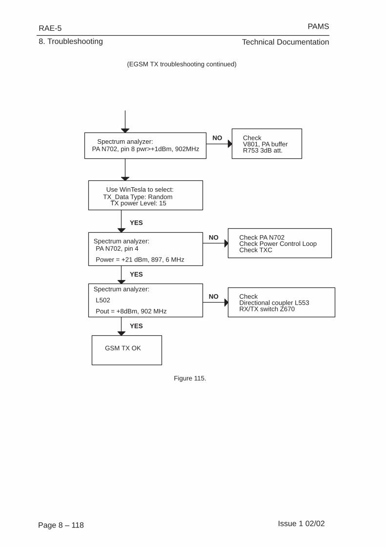
PAMS
Technical Documentation
RAE-5
8. Troubleshooting
Page 8 – 118 Issue 1 02/02
TX_Data Type: RandomUse WinTesla to select:
PA N702, pin 4Spectrum analyzer: NO Check PA N702
Check Power Control Loop
YES
Check TXC
Pout = +8dBm, 902 MHz
Spectrum analyzer:NO Check
Directional coupler L553
YES
RX/TX switch Z670
YES
(EGSM TX troubleshooting continued)
TX power Level: 15
Power = +21 dBm, 897, 6 MHz
L502
GSM TX OK
PA N702, pin 8 pwr>+1dBm, 902MHzSpectrum analyzer: NO Check
V801, PA bufferR753 3dB att.
Figure 115.

PAMS
Technical Documentation
RAE-5
8. Troubleshooting
Page 8 – 119Issue 1 02/02
5.4 PCN Transmitter
General troubleshooting instructions for PCN TX
Apply a RF–cable to the RF–connector to allow the transmitted signal to act asnormal. RF–cable should be connected to measurement equipment or to atleast a 10–dB attenuator, otherwise the PA may be damaged.
Start Wintesla–Service–Software and
Select: Product Alt+p
Band b
PCN p
Select: Testing Alt+e
RF Controls r
TX Power Level: BASE Alt+x, b
TX Continuos Alt+c. . . . . . . . . . . . . . . . . . . . . . . . . . .
TX Data Type: Random Alt+d, r
Channel: 700 Alt+n, 700
Apply Alt+a. . . . . . . .
5.4.1 Path of the transmitted PCN signal
ÏÏÏÏÏÏÏÏÏÏÏÏÏÏÏÏÏÏÏÏÏÏÏÏÏÏÏÏÏÏÏÏÏÏÏÏÏÏÏÏÏÏÏÏÏÏÏÏÏÏÏÏÏÏÏÏÏÏÏÏÏÏÏÏÏÏÏÏÏÏÏÏÏÏÏÏÏÏÏÏÏÏÏÏÏÏÏÏÏÏÏÏÏÏÏÏÏÏÏÏÏÏÏÏÏÏÏÏÏÏÏÏÏÏÏÏÏÏÏÏÏÏÏÏÏÏÏÏÏÏÏÏÏÏÏÏÏÏÏÏÏÏÏÏÏÏÏÏÏÏÏÏÏÏÏÏÏÏÏÏÏÏÏÏÏÏÏÏÏÏÏÏÏÏÏÏÏÏÏÏÏÏÏÏÏÏÏÏÏÏÏÏÏÏÏÏÏÏÏÏÏÏÏÏÏÏÏÏÏÏÏÏÏÏÏÏÏÏÏÏÏÏÏÏ
DET
RX
/TX
Sw
itch
RX
RX
TX
TX
OUTP_D_TX/OUTM_D_TX
OUTP_G_TX/OUTM_G_TX
2
2
Last edit 13:35 07–02–00
Open collector
Open collectorGSM
PCN
VB
AT
TR
F
PWCDET
TX
P
TX
C
Vpctrl_fb
Vpctrl_g
Vpctrl_p
RFControls
VTX_B_G
V_ANT_1/V_ANT_2
2
PA DiplexerDir. Coupler
TXC
TXP
VBATTRF
TXQ_0/TXQ_180
TXI_0/TXI_180
2
2
VTX
VTX_B_G
Antenna connector
Figure 116. EGSM TX signal
Buffer

PAMS
Technical Documentation
RAE-5
8. Troubleshooting
Page 8 – 120 Issue 1 02/02
5.4.2 Troubleshooting diagram for PCN Transmitter
PCN TX Troubleshooting
Check with oscilloscope :
R741 power >0dBm, 1747,6 MHz
YES
R565:: VREF Vdc = 1.5V ?
NO
YES
R700 & R740 VTX Vdc = 2.7 V?TPJ320 TXP Vdc>2.5 V ?C557 VRX Vdc = 2.7 V ?C561 VSYN_2 Vdc = 2.7 V ?C550 VXO Vdc = 2.7 V ?
CheckBaseband
NO
Check with oscilloscope :R546 & C640 TXQ_0 Vac= 0.4Vpp, Vdc=0.8VR546 & C640 TXQ_180 Vac=0.4Vpp, Vdc=0.8V
R541 & C541 TXI_0 Vac=0.4Vpp, Vdc=0.8VR541 & C541 TXI_180 Vac=0.4Vpp, Vdc=0.8V
CheckBaseband
NO
YES
Check with oscilloscope :
R755 TXBUFF Vdc > 2.0 VC789 TXVGSM Vdc < 0.3 VC790 TXVPCN Vdc > 2.0 VC731 TXVDET Vdc > 2.0 V
CheckHagar serial interfaceHagar
Spectrum analyzer: NO Check
Hagar
YES
Z741 (pin 3)Spectrum analyzer: NO Check
YES
Synthesizer
filter Z671
PA N702, pin 8Spectrum analyzer: NO Check
V801 PA buffer
YES
R753 3dB att.
YES
(cont. next page)
power > +6 dBm, 1747,6 MHzDiplex
power > +3 dBm, 1747,6 MHz
Figure 117.

PAMS
Technical Documentation
RAE-5
8. Troubleshooting
Page 8 – 121Issue 1 02/02
TX_Data Type: RandomUse WinTesla to select:
PA N702, pin 4Spectrum analyzer: NO Check PA N702
Check Power Control Loop
YES
Check TXC
Power = +20 dBm, 1747,6 MHz
Spectrum analyzer:NO Check
directional coupler L553
YES
RX/TX switch Z670
YES
(PCN TX troubleshooting continued)
TX power Level: 5
Power = +18 dBm, 1747,6 MHz
L502
PCN TX OK
Figure 118.
PAMS
Technical Documentation
RAE-5
8. Troubleshooting
Page 8 – 122 Issue 1 02/02
5.5 Synthesizer
There is only one PLL synthesiser generating frequencies for both Rx and Tx inboth bands ( PCN and GSM). VCO frequency is divided by 2 or by 4 in HAGARdepending on which band is active.
General troubleshooting instructions for Synthesizer
Start Wintesla–Service–Software and
Select: Product Alt+p
Band b
EGSM e
Select: Testing Alt+e
RF Controls r
RX Continuous Alt+r
Cont. Mode Ch: 60 Alt+o, 60
In this situation there is possible to measure frequency of 3788 MHz at the out-put of the VCO ( G600) using a spectrum analyzer.
5.5.1 26 MHz reference oscillator ( VCTCXO )The 26 MHz oscillator (G803) is used as a reference frequency for the PLL syn-thesiser and as the system clock for BB ( 13 MHz) after it is divided by 2 in HA-GAR. 26 MHz signal from the VCTCXO is approx. 0,8 Vpp. Frequency of thisoscillator is adjusted by dc voltage ( Vcon ) coming from the DAC in COBBA.Range of Vcon is 0.3 – 2.3 V.
5.5.2 VCOThe VCO is generating frequencies in the range of 3420 – 3840 MHz when PLLis in function. These are divided by 2 or by 4 in HAGAR so that they can gener-ate all channels in GSM and PCN. Frequency of the VCO is controlled by dcvoltage ( Vc ) coming from the loop filter. Range of the Vc when PLL is in func-tion is 0.7 – 3.8 V. Even if PLL is not working ( Vc out of range ) there is somefrequency at the output of the VCO ( G600) which is between 3 and 4 GHz, of-couse if the VCO is working.

PAMS
Technical Documentation
RAE-5
8. Troubleshooting
Page 8 – 123Issue 1 02/02
5.5.3 Troubleshooting diagram for PLL Synthesizer
From WinTesla chose:Product > Band > EGSM
Testing > RF Controls >Rx continuous > Ch 60
Spectrum Analyzer
VCO output ( G800 out)
3788 MHz
No
Yes
PLL block functional
Oscilloscope
VCTCXO Power Supply(G830 Vcc)2,7 V
OscilloscopeVCTCXO output
26 MHz,approx. 0.8 Vpp
VCTCXO is dead
Oscilloscope
VCO Power Supply(G800Vcc)
Yes
No
Check CCONTCheck CCONT
Spectrum Analyzer
VCO output ( G800 out)Some signal between 3and 4 GHz
VCO is dead
Check HAGAR,wrong writting to HAGAR(SCLK,SDATA,SLE,
HAGARRESET)
Yes
No No
Yes
Yes
No
(G830 out)
2.7 V
VSYN_2 = 2.7VVCHP (C783) = 4.7V
Figure 119.
It is important to say that power supply for VCTCXO ( VXO) is OFF only in‘Deep Sleep Mode’ and power supply for VCO ( G800 Vcc) is OFF in ‘SleepMode’.

PAMS
Technical Documentation
RAE-5
8. Troubleshooting
Page 8 – 124 Issue 1 02/02
If the phone goes ‘dead’ very short time after the power is turned ON, possiblereason for this might be that 13 MHz system clock signal is not coming to theBB. Use the following chart to find the problem.
Oscilloscope
Turn the phone ONand measure powersupply fo r the VCTCX( G800 Vcc) 2.7 V
Oscilloscope
Measure the outputsignal of the VCTCXO( G830 out) appx.o,8 Vpp, 26 MHz
Oscilloscope
13 MHz buffer inputapprox. 0,3 Vpp
Oscilloscope
13 MHz buffer outputapprox. 0,4 Vpp
Check CCONT, phoneis ’dead’
VCTCXO is ’dead’ Check HAGAR,divider by 2 in HAGARnot in function ( notenabled)
Buffer transistor not infunction ( V800)
Reason is somethingelse ( Software,battery, etc. )
Yes Yes Yes Yes
No No No No
Figure 120.

PAMS
Technical Documentation
RAE-5
8. Troubleshooting
Page 8 – 125Issue 1 02/02
5.5.4 PLL Block Diagram
ÌÌÌÌÌÌÌÌÌÌÌÌÌÌÌÌÌÌÌÌÌÌÌÌÌÌÌÌÌÌÌÌÌÌÌÌÌÌÌÌÌÌÌÌÌÌÌÌÌÌÌÌÌÌÌÌÌÌÌÌÌÌÌÌÌÌÌÌÌÌÌÌÌÌÌÌÌÌÌÌÌÌÌÌÌÌÌÌÌÌÌÌÌÌÌÌÌÌÌÌÌÌÌÌÌÌÌÌÌÌÌÌÌÌÌÌÌÌÌÌÌÌÌÌÌÌÌÌÌÌÌÌÌÌÌÌÌÌÌÌÌÌÌÌÌÌÌÌÌÌÌÌÌÌÌÌÌÌÌÌÌÌÌÌÌÌÌÌÌÌÌÌÌÌÌÌÌÌÌÌÌÌÌÌÌÌÌÌÌÌÌÌÌÌÌÌÌÌÌÌÌÌÌÌÌÌÌÌÌÌÌÌÌÌÌÌÌÌÌÌÌÌÌÌÌÌÌÌÌÌÌÌÌÌÌÌÌÌÌÌÌÌÌÌÌÌÌÌÌÌÌÌÌÌÌÌÌÌÌÌÌÌÌÌÌÌÌÌÌÌÌÌÌÌÌÌÌÌÌÌÌÌÌÌÌÌÌÌÌÌ
64/65 NDIVADIV ϕ charge
pump
RDIV
CTRL
SDATA
SCLK
SLE
1/4 1/2
2
OSC_IN
OUT_CP
2 2 2 2
1/2
1/4
2
2
4 4
44
loopfilter
VCO
AFC
26MHz
Last edit 13:45 07–02–00Drawing12
VDIG
VPRE
VCP/GND_CP2
VLO
Reset
INP_LO/INM_LO
VBB
RFC
VXO
1/2 TOUT
VSYN_1
VSYN_2
AFC
HAGARRESET
SLE
SCLK
SDATA
VCP
VF_RX
3dB
2
Figure 121. PLL

PAMS
Technical Documentation
RAE-5
8. Troubleshooting
Page 8 – 126 Issue 1 02/02
5.6 Frequency lists
Table 6. PCN frequencies and corresponding VCO frequencies
CH TX vco RX(TX+95)
VCO
512 1710.2 3420.4 1805.2 3610.4513 1710.4 3420.8 1805.4 3610.8514 1710.6 3421.2 1805.6 3611.2515 1710.8 3421.6 1805.8 3611.6516 1711.0 3422.0 1806.0 3612.0517 1711.2 3422.4 1806.2 3612.4518 1711.4 3422.8 1806.4 3612.8519 1711.6 3423.2 1806.6 3613.2520 1711.8 3423.6 1806.8 3613.6521 1712.0 3424.0 1807.0 3614.0522 1712.2 3424.4 1807.2 3614.4523 1712.4 3424.8 1807.4 3614.8524 1712.6 3425.2 1807.6 3615.2525 1712.8 3425.6 1807.8 3615.6526 1713.0 3426.0 1808.0 3616.0527 1713.2 3426.4 1808.2 3616.4528 1713.4 3426.8 1808.4 3616.8529 1713.6 3427.2 1808.6 3617.2530 1713.8 3427.6 1808.8 3617.6531 1714.0 3428.0 1809.0 3618.0532 1714.2 3428.4 1809.2 3618.4533 1714.4 3428.8 1809.4 3618.8534 1714.6 3429.2 1809.6 3619.2535 1714.8 3429.6 1809.8 3619.6536 1715.0 3430.0 1810.0 3620.0537 1715.2 3430.4 1810.2 3620.4538 1715.4 3430.8 1810.4 3620.8539 1715.6 3431.2 1810.6 3621.2540 1715.8 3431.6 1810.8 3621.6541 1716.0 3432.0 1811.0 3622.0542 1716.2 3432.4 1811.2 3622.4543 1716.4 3432.8 1811.4 3622.8544 1716.6 3433.2 1811.6 3623.2545 1716.8 3433.6 1811.8 3623.6546 1717.0 3434.0 1812.0 3624.0547 1717.2 3434.4 1812.2 3624.4548 1717.4 3434.8 1812.4 3624.8

PAMS
Technical Documentation
RAE-5
8. Troubleshooting
Page 8 – 127Issue 1 02/02
VCORX (TX+95)
vcoTXCH
549 1717.6 3435.2 1812.6 3625.2550 1717.8 3435.6 1812.8 3625.6551 1718.0 3436.0 1813.0 3626.0552 1718.2 3436.4 1813.2 3626.4553 1718.4 3436.8 1813.4 3626.8554 1718.6 3437.2 1813.6 3627.2555 1718.8 3437.6 1813.8 3627.6556 1719.0 3438.0 1814.0 3628.0557 1719.2 3438.4 1814.2 3628.4558 1719.4 3438.8 1814.4 3628.8559 1719.6 3439.2 1814.6 3629.2560 1719.8 3439.6 1814.8 3629.6561 1720.0 3440.0 1815.0 3630.0562 1720.2 3440.4 1815.2 3630.4563 1720.4 3440.8 1815.4 3630.8564 1720.6 3441.2 1815.6 3631.2565 1720.8 3441.6 1815.8 3631.6566 1721.0 3442.0 1816.0 3632.0567 1721.2 3442.4 1816.2 3632.4568 1721.4 3442.8 1816.4 3632.8569 1721.6 3443.2 1816.6 3633.2570 1721.8 3443.6 1816.8 3633.6571 1722.0 3444.0 1817.0 3634.0572 1722.2 3444.4 1817.2 3634.4573 1722.4 3444.8 1817.4 3634.8574 1722.6 3445.2 1817.6 3635.2575 1722.8 3445.6 1817.8 3635.6576 1723.0 3446.0 1818.0 3636.0577 1723.2 3446.4 1818.2 3636.4578 1723.4 3446.8 1818.4 3636.8579 1723.6 3447.2 1818.6 3637.2580 1723.8 3447.6 1818.8 3637.6581 1724.0 3448.0 1819.0 3638.0582 1724.2 3448.4 1819.2 3638.4583 1724.4 3448.8 1819.4 3638.8584 1724.6 3449.2 1819.6 3639.2585 1724.8 3449.6 1819.8 3639.6586 1725.0 3450.0 1820.0 3640.0587 1725.2 3450.4 1820.2 3640.4588 1725.4 3450.8 1820.4 3640.8589 1725.6 3451.2 1820.6 3641.2590 1725.8 3451.6 1820.8 3641.6

PAMS
Technical Documentation
RAE-5
8. Troubleshooting
Page 8 – 128 Issue 1 02/02
VCORX (TX+95)
vcoTXCH
591 1726.0 3452.0 1821.0 3642.0592 1726.2 3452.4 1821.2 3642.4593 1726.4 3452.8 1821.4 3642.8594 1726.6 3453.2 1821.6 3643.2595 1726.8 3453.6 1821.8 3643.6596 1727.0 3454.0 1822.0 3644.0597 1727.2 3454.4 1822.2 3644.4598 1727.4 3454.8 1822.4 3644.8599 1727.6 3455.2 1822.6 3645.2600 1727.8 3455.6 1822.8 3645.6601 1728.0 3456.0 1823.0 3646.0602 1728.2 3456.4 1823.2 3646.4603 1728.4 3456.8 1823.4 3646.8604 1728.6 3457.2 1823.6 3647.2605 1728.8 3457.6 1823.8 3647.6606 1729.0 3458.0 1824.0 3648.0607 1729.2 3458.4 1824.2 3648.4608 1729.4 3458.8 1824.4 3648.8609 1729.6 3459.2 1824.6 3649.2610 1729.8 3459.6 1824.8 3649.6611 1730.0 3460.0 1825.0 3650.0612 1730.2 3460.4 1825.2 3650.4613 1730.4 3460.8 1825.4 3650.8614 1730.6 3461.2 1825.6 3651.2615 1730.8 3461.6 1825.8 3651.6616 1731.0 3462.0 1826.0 3652.0617 1731.2 3462.4 1826.2 3652.4618 1731.4 3462.8 1826.4 3652.8619 1731.6 3463.2 1826.6 3653.2620 1731.8 3463.6 1826.8 3653.6621 1732.0 3464.0 1827.0 3654.0622 1732.2 3464.4 1827.2 3654.4623 1732.4 3464.8 1827.4 3654.8624 1732.6 3465.2 1827.6 3655.2625 1732.8 3465.6 1827.8 3655.6626 1733.0 3466.0 1828.0 3656.0627 1733.2 3466.4 1828.2 3656.4628 1733.4 3466.8 1828.4 3656.8629 1733.6 3467.2 1828.6 3657.2630 1733.8 3467.6 1828.8 3657.6631 1734.0 3468.0 1829.0 3658.0632 1734.2 3468.4 1829.2 3658.4

PAMS
Technical Documentation
RAE-5
8. Troubleshooting
Page 8 – 129Issue 1 02/02
VCORX (TX+95)
vcoTXCH
633 1734.4 3468.8 1829.4 3658.8634 1734.6 3469.2 1829.6 3659.2635 1734.8 3469.6 1829.8 3659.6636 1735.0 3470.0 1830.0 3660.0637 1735.2 3470.4 1830.2 3660.4638 1735.4 3470.8 1830.4 3660.8639 1735.6 3471.2 1830.6 3661.2640 1735.8 3471.6 1830.8 3661.6641 1736.0 3472.0 1831.0 3662.0642 1736.2 3472.4 1831.2 3662.4643 1736.4 3472.8 1831.4 3662.8644 1736.6 3473.2 1831.6 3663.2645 1736.8 3473.6 1831.8 3663.6646 1737.0 3474.0 1832.0 3664.0647 1737.2 3474.4 1832.2 3664.4648 1737.4 3474.8 1832.4 3664.8649 1737.6 3475.2 1832.6 3665.2650 1737.8 3475.6 1832.8 3665.6651 1738.0 3476.0 1833.0 3666.0652 1738.2 3476.4 1833.2 3666.4653 1738.4 3476.8 1833.4 3666.8654 1738.6 3477.2 1833.6 3667.2655 1738.8 3477.6 1833.8 3667.6656 1739.0 3478.0 1834.0 3668.0657 1739.2 3478.4 1834.2 3668.4658 1739.4 3478.8 1834.4 3668.8659 1739.6 3479.2 1834.6 3669.2660 1739.8 3479.6 1834.8 3669.6661 1740.0 3480.0 1835.0 3670.0662 1740.2 3480.4 1835.2 3670.4663 1740.4 3480.8 1835.4 3670.8664 1740.6 3481.2 1835.6 3671.2665 1740.8 3481.6 1835.8 3671.6666 1741.0 3482.0 1836.0 3672.0667 1741.2 3482.4 1836.2 3672.4668 1741.4 3482.8 1836.4 3672.8669 1741.6 3483.2 1836.6 3673.2670 1741.8 3483.6 1836.8 3673.6671 1742.0 3484.0 1837.0 3674.0672 1742.2 3484.4 1837.2 3674.4673 1742.4 3484.8 1837.4 3674.8674 1742.6 3485.2 1837.6 3675.2

PAMS
Technical Documentation
RAE-5
8. Troubleshooting
Page 8 – 130 Issue 1 02/02
VCORX (TX+95)
vcoTXCH
675 1742.8 3485.6 1837.8 3675.6676 1743.0 3486.0 1838.0 3676.0677 1743.2 3486.4 1838.2 3676.4678 1743.4 3486.8 1838.4 3676.8679 1743.6 3487.2 1838.6 3677.2680 1743.8 3487.6 1838.8 3677.6681 1744.0 3488.0 1839.0 3678.0682 1744.2 3488.4 1839.2 3678.4683 1744.4 3488.8 1839.4 3678.8684 1744.6 3489.2 1839.6 3679.2685 1744.8 3489.6 1839.8 3679.6686 1745.0 3490.0 1840.0 3680.0687 1745.2 3490.4 1840.2 3680.4688 1745.4 3490.8 1840.4 3680.8689 1745.6 3491.2 1840.6 3681.2690 1745.8 3491.6 1840.8 3681.6691 1746.0 3492.0 1841.0 3682.0692 1746.2 3492.4 1841.2 3682.4693 1746.4 3492.8 1841.4 3682.8694 1746.6 3493.2 1841.6 3683.2695 1746.8 3493.6 1841.8 3683.6696 1747.0 3494.0 1842.0 3684.0697 1747.2 3494.4 1842.2 3684.4698 1747.4 3494.8 1842.4 3684.8699 1747.6 3495.2 1842.6 3685.2700 1747.8 3495.6 1842.8 3685.6701 1748.0 3496.0 1843.0 3686.0702 1748.2 3496.4 1843.2 3686.4703 1748.4 3496.8 1843.4 3686.8704 1748.6 3497.2 1843.6 3687.2705 1748.8 3497.6 1843.8 3687.6706 1749.0 3498.0 1844.0 3688.0707 1749.2 3498.4 1844.2 3688.4708 1749.4 3498.8 1844.4 3688.8709 1749.6 3499.2 1844.6 3689.2710 1749.8 3499.6 1844.8 3689.6711 1750.0 3500.0 1845.0 3690.0712 1750.2 3500.4 1845.2 3690.4713 1750.4 3500.8 1845.4 3690.8714 1750.6 3501.2 1845.6 3691.2715 1750.8 3501.6 1845.8 3691.6716 1751.0 3502.0 1846.0 3692.0

PAMS
Technical Documentation
RAE-5
8. Troubleshooting
Page 8 – 131Issue 1 02/02
VCORX (TX+95)
vcoTXCH
717 1751.2 3502.4 1846.2 3692.4718 1751.4 3502.8 1846.4 3692.8719 1751.6 3503.2 1846.6 3693.2720 1751.8 3503.6 1846.8 3693.6721 1752.0 3504.0 1847.0 3694.0722 1752.2 3504.4 1847.2 3694.4723 1752.4 3504.8 1847.4 3694.8724 1752.6 3505.2 1847.6 3695.2725 1752.8 3505.6 1847.8 3695.6726 1753.0 3506.0 1848.0 3696.0727 1753.2 3506.4 1848.2 3696.4728 1753.4 3506.8 1848.4 3696.8729 1753.6 3507.2 1848.6 3697.2730 1753.8 3507.6 1848.8 3697.6731 1754.0 3508.0 1849.0 3698.0732 1754.2 3508.4 1849.2 3698.4733 1754.4 3508.8 1849.4 3698.8734 1754.6 3509.2 1849.6 3699.2735 1754.8 3509.6 1849.8 3699.6736 1755.0 3510.0 1850.0 3700.0737 1755.2 3510.4 1850.2 3700.4738 1755.4 3510.8 1850.4 3700.8739 1755.6 3511.2 1850.6 3701.2740 1755.8 3511.6 1850.8 3701.6741 1756.0 3512.0 1851.0 3702.0742 1756.2 3512.4 1851.2 3702.4743 1756.4 3512.8 1851.4 3702.8744 1756.6 3513.2 1851.6 3703.2745 1756.8 3513.6 1851.8 3703.6746 1757.0 3514.0 1852.0 3704.0747 1757.2 3514.4 1852.2 3704.4748 1757.4 3514.8 1852.4 3704.8749 1757.6 3515.2 1852.6 3705.2750 1757.8 3515.6 1852.8 3705.6751 1758.0 3516.0 1853.0 3706.0752 1758.2 3516.4 1853.2 3706.4753 1758.4 3516.8 1853.4 3706.8754 1758.6 3517.2 1853.6 3707.2755 1758.8 3517.6 1853.8 3707.6756 1759.0 3518.0 1854.0 3708.0757 1759.2 3518.4 1854.2 3708.4758 1759.4 3518.8 1854.4 3708.8

PAMS
Technical Documentation
RAE-5
8. Troubleshooting
Page 8 – 132 Issue 1 02/02
VCORX (TX+95)
vcoTXCH
759 1759.6 3519.2 1854.6 3709.2760 1759.8 3519.6 1854.8 3709.6761 1760.0 3520.0 1855.0 3710.0762 1760.2 3520.4 1855.2 3710.4763 1760.4 3520.8 1855.4 3710.8764 1760.6 3521.2 1855.6 3711.2765 1760.8 3521.6 1855.8 3711.6766 1761.0 3522.0 1856.0 3712.0767 1761.2 3522.4 1856.2 3712.4768 1761.4 3522.8 1856.4 3712.8769 1761.6 3523.2 1856.6 3713.2770 1761.8 3523.6 1856.8 3713.6771 1762.0 3524.0 1857.0 3714.0772 1762.2 3524.4 1857.2 3714.4773 1762.4 3524.8 1857.4 3714.8774 1762.6 3525.2 1857.6 3715.2775 1762.8 3525.6 1857.8 3715.6776 1763.0 3526.0 1858.0 3716.0777 1763.2 3526.4 1858.2 3716.4778 1763.4 3526.8 1858.4 3716.8779 1763.6 3527.2 1858.6 3717.2780 1763.8 3527.6 1858.8 3717.6781 1764.0 3528.0 1859.0 3718.0782 1764.2 3528.4 1859.2 3718.4783 1764.4 3528.8 1859.4 3718.8784 1764.6 3529.2 1859.6 3719.2785 1764.8 3529.6 1859.8 3719.6786 1765.0 3530.0 1860.0 3720.0787 1765.2 3530.4 1860.2 3720.4788 1765.4 3530.8 1860.4 3720.8789 1765.6 3531.2 1860.6 3721.2790 1765.8 3531.6 1860.8 3721.6791 1766.0 3532.0 1861.0 3722.0792 1766.2 3532.4 1861.2 3722.4793 1766.4 3532.8 1861.4 3722.8794 1766.6 3533.2 1861.6 3723.2795 1766.8 3533.6 1861.8 3723.6796 1767.0 3534.0 1862.0 3724.0797 1767.2 3534.4 1862.2 3724.4798 1767.4 3534.8 1862.4 3724.8799 1767.6 3535.2 1862.6 3725.2800 1767.8 3535.6 1862.8 3725.6

PAMS
Technical Documentation
RAE-5
8. Troubleshooting
Page 8 – 133Issue 1 02/02
VCORX (TX+95)
vcoTXCH
801 1768.0 3536.0 1863.0 3726.0802 1768.2 3536.4 1863.2 3726.4803 1768.4 3536.8 1863.4 3726.8804 1768.6 3537.2 1863.6 3727.2805 1768.8 3537.6 1863.8 3727.6806 1769.0 3538.0 1864.0 3728.0807 1769.2 3538.4 1864.2 3728.4808 1769.4 3538.8 1864.4 3728.8809 1769.6 3539.2 1864.6 3729.2810 1769.8 3539.6 1864.8 3729.6811 1770.0 3540.0 1865.0 3730.0812 1770.2 3540.4 1865.2 3730.4813 1770.4 3540.8 1865.4 3730.8814 1770.6 3541.2 1865.6 3731.2815 1770.8 3541.6 1865.8 3731.6816 1771.0 3542.0 1866.0 3732.0817 1771.2 3542.4 1866.2 3732.4818 1771.4 3542.8 1866.4 3732.8819 1771.6 3543.2 1866.6 3733.2820 1771.8 3543.6 1866.8 3733.6821 1772.0 3544.0 1867.0 3734.0822 1772.2 3544.4 1867.2 3734.4823 1772.4 3544.8 1867.4 3734.8824 1772.6 3545.2 1867.6 3735.2825 1772.8 3545.6 1867.8 3735.6826 1773.0 3546.0 1868.0 3736.0827 1773.2 3546.4 1868.2 3736.4828 1773.4 3546.8 1868.4 3736.8829 1773.6 3547.2 1868.6 3737.2830 1773.8 3547.6 1868.8 3737.6831 1774.0 3548.0 1869.0 3738.0832 1774.2 3548.4 1869.2 3738.4833 1774.4 3548.8 1869.4 3738.8834 1774.6 3549.2 1869.6 3739.2835 1774.8 3549.6 1869.8 3739.6836 1775.0 3550.0 1870.0 3740.0837 1775.2 3550.4 1870.2 3740.4838 1775.4 3550.8 1870.4 3740.8839 1775.6 3551.2 1870.6 3741.2840 1775.8 3551.6 1870.8 3741.6841 1776.0 3552.0 1871.0 3742.0842 1776.2 3552.4 1871.2 3742.4

PAMS
Technical Documentation
RAE-5
8. Troubleshooting
Page 8 – 134 Issue 1 02/02
VCORX (TX+95)
vcoTXCH
843 1776.4 3552.8 1871.4 3742.8
844 1776.6 3553.2 1871.6 3743.2
845 1776.8 3553.6 1871.8 3743.6
846 1777.0 3554.0 1872.0 3744.0
847 1777.2 3554.4 1872.2 3744.4
848 1777.4 3554.8 1872.4 3744.8
849 1777.6 3555.2 1872.6 3745.2
850 1777.8 3555.6 1872.8 3745.6
851 1778.0 3556.0 1873.0 3746.0
852 1778.2 3556.4 1873.2 3746.4
853 1778.4 3556.8 1873.4 3746.8
854 1778.6 3557.2 1873.6 3747.2
855 1778.8 3557.6 1873.8 3747.6
856 1779.0 3558.0 1874.0 3748.0
857 1779.2 3558.4 1874.2 3748.4
858 1779.4 3558.8 1874.4 3748.8
859 1779.6 3559.2 1874.6 3749.2
860 1779.8 3559.6 1874.8 3749.6
861 1780.0 3560.0 1875.0 3750.0
862 1780.2 3560.4 1875.2 3750.4
863 1780.4 3560.8 1875.4 3750.8
864 1780.6 3561.2 1875.6 3751.2
865 1780.8 3561.6 1875.8 3751.6
866 1781.0 3562.0 1876.0 3752.0
867 1781.2 3562.4 1876.2 3752.4
868 1781.4 3562.8 1876.4 3752.8
869 1781.6 3563.2 1876.6 3753.2
870 1781.8 3563.6 1876.8 3753.6
871 1782.0 3564.0 1877.0 3754.0
872 1782.2 3564.4 1877.2 3754.4
873 1782.4 3564.8 1877.4 3754.8
874 1782.6 3565.2 1877.6 3755.2
875 1782.8 3565.6 1877.8 3755.6
876 1783.0 3566.0 1878.0 3756.0
877 1783.2 3566.4 1878.2 3756.4
878 1783.4 3566.8 1878.4 3756.8
879 1783.6 3567.2 1878.6 3757.2
880 1783.8 3567.6 1878.8 3757.6
881 1784.0 3568.0 1879.0 3758.0
882 1784.2 3568.4 1879.2 3758.4
883 1784.4 3568.8 1879.4 3758.8

PAMS
Technical Documentation
RAE-5
8. Troubleshooting
Page 8 – 135Issue 1 02/02
VCORX (TX+95)
vcoTXCH
884 1784.6 3569.2 1879.6 3759.2885 1784.8 3569.6 1879.8 3759.6
Table 7. GSM frequencies and corresponding VCO frequencies
CH TX vco RX(TX+95)
VCO
975 880.2 3520.8 925.2 3700.8
976 880.4 3521.6 925.4 3701.6
977 880.6 3522.4 925.6 3702.4
978 880.8 3523.2 925.8 3703.2
979 881.0 3524.0 926.0 3704.0
980 881.2 3524.8 926.2 3704.8
981 881.4 3525.6 926.4 3705.6
982 881.6 3526.4 926.6 3706.4
983 881.8 3527.2 926.8 3707.2
984 882.0 3528.0 927.0 3708.0
985 882.2 3528.8 927.2 3708.8
986 882.4 3529.6 927.4 3709.6
987 882.6 3530.4 927.6 3710.4
988 882.8 3531.2 927.8 3711.2
989 883.0 3532.0 928.0 3712.0
990 883.2 3532.8 928.2 3712.8
991 883.4 3533.6 928.4 3713.6
992 883.6 3534.4 928.6 3714.4
993 883.8 3535.2 928.8 3715.2
994 884.0 3536.0 929.0 3716.0
995 884.2 3536.8 929.2 3716.8
996 884.4 3537.6 929.4 3717.6
997 884.6 3538.4 929.6 3718.4
998 884.8 3539.2 929.8 3719.2
999 885.0 3540.0 930.0 3720.0
1000 885.2 3540.8 930.2 3720.8
1001 885.4 3541.6 930.4 3721.6
1002 885.6 3542.4 930.6 3722.4
1003 885.8 3543.2 930.8 3723.2
1004 886.0 3544.0 931.0 3724.0
1005 886.2 3544.8 931.2 3724.8
1006 886.4 3545.6 931.4 3725.6
1007 886.6 3546.4 931.6 3726.4
1008 886.8 3547.2 931.8 3727.2

PAMS
Technical Documentation
RAE-5
8. Troubleshooting
Page 8 – 136 Issue 1 02/02
Table 7. GSM frequencies and corresponding VCO frequencies
VCORX(TX+95)
vcoTXCH
1009 887.0 3548.0 932.0 3728.0
1010 887.2 3548.8 932.2 3728.8
1011 887.4 3549.6 932.4 3729.6
1012 887.6 3550.4 932.6 3730.4
1013 887.8 3551.2 932.8 3731.2
1014 888.0 3552.0 933.0 3732.0
1015 888.2 3552.8 933.2 3732.8
1016 888.4 3553.6 933.4 3733.6
1017 888.6 3554.4 933.6 3734.4
1018 888.8 3555.2 933.8 3735.2
1019 889.0 3556.0 934.0 3736.0
1020 889.2 3556.8 934.2 3736.8
1021 889.4 3557.6 934.4 3737.6
1022 889.6 3558.4 934.6 3738.4
1023 889.8 3559.2 934.8 3739.2
0 890.0 3560.0 935.0 3740.0
1 890.2 3560.8 935.2 3740.8
2 890.4 3561.6 935.4 3741.6
3 890.6 3562.4 935.6 3742.4
4 890.8 3563.2 935.8 3743.2
5 891.0 3564.0 936.0 3744.0
6 891.2 3564.8 936.2 3744.8
7 891.4 3565.6 936.4 3745.6
8 891.6 3566.4 936.6 3746.4
9 891.8 3567.2 936.8 3747.2
10 892.0 3568.0 937.0 3748.0
11 892.2 3568.8 937.2 3748.8
12 892.4 3569.6 937.4 3749.6
13 892.6 3570.4 937.6 3750.4
14 892.8 3571.2 937.8 3751.2
15 893.0 3572.0 938.0 3752.0
16 893.2 3572.8 938.2 3752.8
17 893.4 3573.6 938.4 3753.6
18 893.6 3574.4 938.6 3754.4
19 893.8 3575.2 938.8 3755.2
20 894.0 3576.0 939.0 3756.0
21 894.2 3576.8 939.2 3756.8
22 894.4 3577.6 939.4 3757.6

PAMS
Technical Documentation
RAE-5
8. Troubleshooting
Page 8 – 137Issue 1 02/02
Table 7. GSM frequencies and corresponding VCO frequencies
VCORX(TX+95)
vcoTXCH
23 894.6 3578.4 939.6 3758.4
24 894.8 3579.2 939.8 3759.2
25 895.0 3580.0 940.0 3760.0
26 895.2 3580.8 940.2 3760.8
27 895.4 3581.6 940.4 3761.6
28 895.6 3582.4 940.6 3762.4
29 895.8 3583.2 940.8 3763.2
30 896.0 3584.0 941.0 3764.0
31 896.2 3584.8 941.2 3764.8
32 896.4 3585.6 941.4 3765.6
33 896.6 3586.4 941.6 3766.4
34 896.8 3587.2 941.8 3767.2
35 897.0 3588.0 942.0 3768.0
36 897.2 3588.8 942.2 3768.8
37 897.4 3589.6 942.4 3769.6
38 897.6 3590.4 942.6 3770.4
39 897.8 3591.2 942.8 3771.2
40 898.0 3592.0 943.0 3772.0
41 898.2 3592.8 943.2 3772.8
42 898.4 3593.6 943.4 3773.6
43 898.6 3594.4 943.6 3774.4
44 898.8 3595.2 943.8 3775.2
45 899.0 3596.0 944.0 3776.0
46 899.2 3596.8 944.2 3776.8
47 899.4 3597.6 944.4 3777.6
48 899.6 3598.4 944.6 3778.4
49 899.8 3599.2 944.8 3779.2
50 900.0 3600.0 945.0 3780.0
51 900.2 3600.8 945.2 3780.8
52 900.4 3601.6 945.4 3781.6
53 900.6 3602.4 945.6 3782.4
54 900.8 3603.2 945.8 3783.2
55 901.0 3604.0 946.0 3784.0
56 901.2 3604.8 946.2 3784.8
57 901.4 3605.6 946.4 3785.6
58 901.6 3606.4 946.6 3786.4
59 901.8 3607.2 946.8 3787.2
60 902.0 3608.0 947.0 3788.0

PAMS
Technical Documentation
RAE-5
8. Troubleshooting
Page 8 – 138 Issue 1 02/02
Table 7. GSM frequencies and corresponding VCO frequencies
VCORX(TX+95)
vcoTXCH
61 902.2 3608.8 947.2 3788.8
62 902.4 3609.6 947.4 3789.6
63 902.6 3610.4 947.6 3790.4
64 902.8 3611.2 947.8 3791.2
65 903.0 3612.0 948.0 3792.0
66 903.2 3612.8 948.2 3792.8
67 903.4 3613.6 948.4 3793.6
68 903.6 3614.4 948.6 3794.4
69 903.8 3615.2 948.8 3795.2
70 904.0 3616.0 949.0 3796.0
71 904.2 3616.8 949.2 3796.8
72 904.4 3617.6 949.4 3797.6
73 904.6 3618.4 949.6 3798.4
74 904.8 3619.2 949.8 3799.2
75 905.0 3620.0 950.0 3800.0
76 905.2 3620.8 950.2 3800.8
77 905.4 3621.6 950.4 3801.6
78 905.6 3622.4 950.6 3802.4
79 905.8 3623.2 950.8 3803.2
80 906.0 3624.0 951.0 3804.0
81 906.2 3624.8 951.2 3804.8
82 906.4 3625.6 951.4 3805.6
83 906.6 3626.4 951.6 3806.4
84 906.8 3627.2 951.8 3807.2
85 907.0 3628.0 952.0 3808.0
86 907.2 3628.8 952.2 3808.8
87 907.4 3629.6 952.4 3809.6
88 907.6 3630.4 952.6 3810.4
89 907.8 3631.2 952.8 3811.2
90 908.0 3632.0 953.0 3812.0
91 908.2 3632.8 953.2 3812.8
92 908.4 3633.6 953.4 3813.6
93 908.6 3634.4 953.6 3814.4
94 908.8 3635.2 953.8 3815.2
95 909.0 3636.0 954.0 3816.0
96 909.2 3636.8 954.2 3816.8
97 909.4 3637.6 954.4 3817.6
98 909.6 3638.4 954.6 3818.4

PAMS
Technical Documentation
RAE-5
8. Troubleshooting
Page 8 – 139Issue 1 02/02
Table 7. GSM frequencies and corresponding VCO frequencies
VCORX(TX+95)
vcoTXCH
99 909.8 3639.2 954.8 3819.2
100 910.0 3640.0 955.0 3820.0
101 910.2 3640.8 955.2 3820.8
102 910.4 3641.6 955.4 3821.6
103 910.6 3642.4 955.6 3822.4
104 910.8 3643.2 955.8 3823.2
105 911.0 3644.0 956.0 3824.0
106 911.2 3644.8 956.2 3824.8
107 911.4 3645.6 956.4 3825.6
108 911.6 3646.4 956.6 3826.4
109 911.8 3647.2 956.8 3827.2
110 912.0 3648.0 957.0 3828.0
111 912.2 3648.8 957.2 3828.8
112 912.4 3649.6 957.4 3829.6
113 912.6 3650.4 957.6 3830.4
114 912.8 3651.2 957.8 3831.2
115 913.0 3652.0 958.0 3832.0
116 913.2 3652.8 958.2 3832.8
117 913.4 3653.6 958.4 3833.6
118 913.6 3654.4 958.6 3834.4
119 913.8 3655.2 958.8 3835.2
120 914.0 3656.0 959.0 3836.0
121 914.2 3656.8 959.2 3836.8
122 914.4 3657.6 959.4 3837.6
123 914.6 3658.4 959.6 3838.4
124 914.8 3659.2 959.8 3839.2

PAMS
Technical Documentation
RAE-5
8. Troubleshooting
Page 8 – 140 Issue 1 02/02
6 Diagrams of Test Points
Diagrams of test points, refer to Section 11, Service Instructions.
[] 1

PAMS Technical Documentation
RAE-5 Series PDA
Issue 1 04/2002 Copyright 2002. Nokia Corporation. All Rights Reserved.
9. Schematic diagrams

PAMS
Technical Documentation
RAE-5
9. Schematic diagrams
Page 09 – 2Issue 1 04/2002
AMENDMENT RECORD SHEET
AmendmentNumber
Date Inserted By Comments
04/2002 OJuntunen

PAMS
Technical Documentation
RAE-5
9. Schematic diagrams
Page 09 – 3Issue 1 04/2002
CONTENTS –Schematic Diagrams
Page No
Block Diagram of UL1_07 QWERTY keypad (Version 0.0 Edit 139)09 – 4. . . . . . . . . . . . . . . . . . . . . . . . . . . . . . . . . . . . . . . . . . . . . . . . . . . . . . .
Block Diagram of UL1_07 CMT keyboard and PDA soft keys (Version 0.0 Edit 22)09 – 5. . . . . . . . . . . . . . . . . . . . . . . . . . . . . . . . . . . . . . . . . . . . . . . . . . . . . . .
Circuit Diagram of UL1_07 D–TFD power interface (Version 0.0 Edit 126)09 – 6. . . . . . . . . . . . . . . . . . . . . . . . . . . . . . . . . . . . . . . . . . . . . . . . . . . . . . .
Circuit Diagram of UL1_07 CMT UI LEDs (Version 0.0 Edit 28) 09 – 7
Circuit Diagram of UL1_07 PDA backlight (Version 0.0 Edit 40) 09 – 8
Parts Placement Diagram of UL1_07 1/2 09 – 9. . . . . . . . . . . . . . . . . .
Parts Placement Diagram of UL1_07 2/2 09 – 10. . . . . . . . . . . . . . . . . .
Block Diagram of KL8_05 System (Version 0.2 Edit 114) 09 – 11. . . .
Circuit Diagram of KL8_05 System Connector (Version 0.0 Edit 125)09 – 12. . . . . . . . . . . . . . . . . . . . . . . . . . . . . . . . . . . . . . . . . . . . . . . . . . . . . . .
Circuit Diagram of KL8_05 Audio RFI (Version 0.0 Edit 144) 09 – 13.
Circuit Diagram of KL8_05 CPU (Version 0.0 Edit 167) 09 – 14. . . . . .
Circuit Diagram of KL8_05 IRDA (Version 0.0 Edit 167) 09 – 15. . . . .
Circuit Diagram of KL8_05 memories (Version 0.0 Edit 106) 09 – 16.
Circuit Diagram of KL8_05 MMC (Version 0.0 Edit 73) 09 – 17. . . . . . .
Circuit Diagram of KL8_05 Power (Version 0.0 Edit 216) 09 – 18. . . . .
Circuit Diagram of KL8_05 User interface (Version 0.0 Edit 83) 09 – 19
Circuit Diagram of KL8_05 BB/RF Connector (Version 0.2 Edit 114)09 – 20. . . . . . . . . . . . . . . . . . . . . . . . . . . . . . . . . . . . . . . . . . . . . . . . . . . . . . .
Circuit Diagram of KL8_05 RF (Version 0.2 Edit 197) 09 – 21. . . . . . . .
Parts Placement Diagram of KL8_05 1/2 09 – 22. . . . . . . . . . . . . . . . . .
Parts Placement Diagram of KL8_05 2/2 09 – 23. . . . . . . . . . . . . . . . . .

PAMS
Technical Documentation
RAE-5
9. Schematic diagrams
Page 09 – 4Issue 1 04/2002
Block Diagram of UL1_07 QWERTY keypad (Version 0.0 Edit 139)
UL1_06

PAMS
Technical Documentation
RAE-5
9. Schematic diagrams
Page 09 – 5Issue 1 04/2002
Block Diagram of UL1_07 CMT keyboard and PDA soft keys (Version 0.0 Edit 22)

PAMS
Technical Documentation
RAE-5
9. Schematic diagrams
Page 09 – 6Issue 1 04/2002
Circuit Diagram of UL1_07 D–TFD power interface (Version 0.0 Edit 126)
UL1_06

PAMS
Technical Documentation
RAE-5
9. Schematic diagrams
Page 09 – 7Issue 1 04/2002
Circuit Diagram of UL1_07 CMT UI LEDs (Version 0.0 Edit 28)

PAMS
Technical Documentation
RAE-5
9. Schematic diagrams
Page 09 – 8Issue 1 04/2002
Circuit Diagram of UL1_07 PDA backlight (Version 0.0 Edit 40)
UL1_06

PAMS
Technical Documentation
RAE-5
9. Schematic diagrams
Page 09 – 9Issue 1 04/2002
Parts Placement Diagram of UL1_07 1/2

PAMS
Technical Documentation
RAE-5
9. Schematic diagrams
Page 09 – 10Issue 1 04/2002
Parts Placement Diagram of UL1_07 2/2

PAMS
Technical Documentation
RAE-5
9. Schematic diagrams
Page 09 – 11Issue 1 04/2002
Block Diagram of KL8_05 System (Version 0.2 Edit 114)

PAMS
Technical Documentation
RAE-5
9. Schematic diagrams
Page 09 – 12Issue 1 04/2002
Circuit Diagram of KL8_05 System Connector (Version 0.0 Edit 125)
Linda HWID K3110
KL8_05 syscon

PAMS
Technical Documentation
RAE-5
9. Schematic diagrams
Page 09 – 13Issue 1 04/2002
Circuit Diagram of KL8_05 Audio RFI (Version 0.0 Edit 144)
KL8_05 audio_rfi
Linda HWID K3110

PAMS
Technical Documentation
RAE-5
9. Schematic diagrams
Page 09 – 14Issue 1 04/2002
Circuit Diagram of KL8_05 CPU (Version 0.0 Edit 167)
KL8
_05
cpu
Lind
a H
WID
K31
10

PAMS
Technical Documentation
RAE-5
9. Schematic diagrams
Page 09 – 15Issue 1 04/2002
Circuit Diagram of KL8_05 IRDA (Version 0.0 Edit 167)

PAMS
Technical Documentation
RAE-5
9. Schematic diagrams
Page 09 – 16Issue 1 04/2002
Circuit Diagram of KL8_05 memories (Version 0.0 Edit 106)
Linda HWID K3110
KL8_05 memories

PAMS
Technical Documentation
RAE-5
9. Schematic diagrams
Page 09 – 17Issue 1 04/2002
Circuit Diagram of KL8_05 MMC (Version 0.0 Edit 73)

PAMS
Technical Documentation
RAE-5
9. Schematic diagrams
Page 09 – 18Issue 1 04/2002
Circuit Diagram of KL8_05 Power (Version 0.0 Edit 216)
KL8_05 power
Not assembled
Not assembled
Linda HWID K3110

PAMS
Technical Documentation
RAE-5
9. Schematic diagrams
Page 09 – 19Issue 1 04/2002
Circuit Diagram of KL8_05 User interface (Version 0.0 Edit 83)
Linda HWID K3110
KL8_05 ui

PAMS
Technical Documentation
RAE-5
9. Schematic diagrams
Page 09 – 20Issue 1 04/2002
Circuit Diagram of KL8_05 BB/RF Connector (Version 0.2 Edit 114)

PAMS
Technical Documentation
RAE-5
9. Schematic diagrams
Page 09 – 21Issue 1 04/2002
Circuit Diagram of KL8_05 RF (Version 0.2 Edit 197)
Vdd_bb+LNA
LNA2+mixer+DTOS
TOO HIGH VOLT
Not assembled
Not assembled
LAYER_4
Wide connection
Not assembled
below component
Not assembled
Wide connection
Modulator
Not assembled
below component
Not assembled
Wide connection
LAYER_4
LAY
ER
_4
Dividers+LO–buffers+prescaler+VCO
Charge pump
KL8_05
below component
below component
VCTCXO
Wide connection
Not assembled
Not assembled

PAMS
Technical Documentation
RAE-5
9. Schematic diagrams
Page 09 – 22Issue 1 04/2002
Parts Placement Diagram of KL8_05 1/2

PAMS
Technical Documentation
RAE-5
9. Schematic diagrams
Page 09 – 23Issue 1 04/2002
Parts Placement Diagram of KL8_05 2/2

PAMS Technical DocumentationRAE-5 Communicator
Issue 1 02/02 Copyright 2002. Nokia Corporation. All Rights Reserved.
10. Parts Lists

PAMS
Technical Documentation
RAE-5
10. Parts Lists
Page 10 – 2 Issue 1 02/02
AMENDMENT RECORD SHEET
AmendmentNumber
Date Inserted By Comments
02/02 OJuntunen

PAMS
Technical Documentation
RAE-5
10. Parts Lists
Page 10 – 3Issue 1 02/02
CONTENTS –Troubleshooting
Page No
Foreword 4. . . . . . . . . . . . . . . . . . . . . . . . . . . . . . . . . . . . . . . . . . . . . .
PDA modules 4. . . . . . . . . . . . . . . . . . . . . . . . . . . . . . . . . . . . . . . . Exploded Diagram, CMT Parts 5. . . . . . . . . . . . . . . . . . . . . . . . . Exploded Diagram, PDA Parts 6. . . . . . . . . . . . . . . . . . . . . . . . .
Exploded Diagram Parts List 7. . . . . . . . . . . . . . . . . . . . . . . . . . . . .

PAMS
Technical Documentation
RAE-5
10. Parts Lists
Page 10 – 4 Issue 1 02/02
Foreword
This section of the service manual contains specific details for the RAE-5 spare parts and modules.
Exploded Diagram 1/2
46

PAMS
Technical Documentation
RAE-5
10. Parts Lists
Page 10 – 5Issue 1 02/02
Exploded Diagram 2/2
45

PAMS
Technical Documentation
RAE-5
10. Parts Lists
Page 10 – 6 Issue 1 02/02
Exploded Diagram Parts List
Mechanical assembly parts 0261997
Part Number inExploded View
Part Name Material Code
1 – 5 Front cover assembly 9467043
6 Phone keymat 9794032
7 CMT display 4850177
8 Colour UI Module UL2 0201785
9 PDA Display 4850167
10 – 19 Frame assembly 9467039
20 Antenna 0660214
21 Antenna pin 9517065
22 Flex cover 9460357
23 QWERTY keypad Refer to the variant section of the manual
24 QWERTY/Flex Module UL8 0201667
25 Chassis assembly 9547013
26 RF/SystemModule KL9
27 Backup battery 4700125
28 – 32 Audio holder assembly 9467044
33 Earpiece 5140067
34 Earpiece gasket 9480565
35 Battery latch assembly 9467045
36 – 41 Back cover assembly 9456810
36 – 41 Back cover assembly 9456810
40 Connector
41 Connector
42 Card cover 9451767
43 Plug 9470114
45 Screw M1.6x7 T6 FeZn black, 8 pcs 6190013
45 Screw M1.6x4 T6 FeZn yellow, 2 pcs 6190023
RF/SystemModule KL8
QWERTY/Flex Module UL8 0201667
Colour UI Module DL1 with LCDs 0201784
Colour UI Module UL2 without LCDs 0201785

PAMS
Technical Documentation
RAE-5
10. Parts Lists
Page 10 – 7Issue 1 02/02
Parts Lists
Engine Module KL8 (EDMS V.3.3)
ITEM CODE DESCRIPTION VALUE TYPE
R001 1430804 Chipres 0w06 100k j R002 1430778 Chipres 0w06 10k j R003 1430726 Chipres 0w06 100r j R004 1430726 Chipres 0w06 100r j R005 1430726 Chipres 0w06 100r j R006 1430762 Chipres 0w06 2k2 j R007 1825019 Chip varistor vwm5.6v vc VCR050 1412279 Chipres 0w1 2r2 j R052 1412279 Chipres 0w1 2r2 j R053 1412279 Chipres 0w1 2r2 j R055 1412279 Chipres 0w1 2r2 j R101 1419003 Chipres 0w5 0r22 j 200pp 200PPR102 1430778 Chipres 0w06 10k j R104 1430804 Chipres 0w06 100k j R105 1430804 Chipres 0w06 100k j R107 1430796 Chipres 0w06 47k j R108 1430804 Chipres 0w06 100k j R109 1430726 Chipres 0w06 100r j R111 1430770 Chipres 0w06 4k7 j R112 1430718 Chipres 0w06 47r j R113 1430796 Chipres 0w06 47k j R114 1430826 Chipres 0w06 680k j R115 1430834 Chipres 0w06 3m3 j R116 1430273 Chipres 0w06 44k2 f 100p 100PR118 1430754 Chipres 0w06 1k0 j R119 1430423 Chipres 0w06 97k6 f 100p 100PR121 1430778 Chipres 0w06 10k j R122 1620025 Res network 0w06 2x100k 2x100k R123 1430778 Chipres 0w06 10k j R124 1430834 Chipres 0w06 3m3 j R125 1430726 Chipres 0w06 100r j R200 1430796 Chipres 0w06 47k j R201 1430681 Chipres 0w06 4r3 j R202 1430762 Chipres 0w06 2k2 j R203 1430788 Chipres 0w06 22k j R204 1430681 Chipres 0w06 4r3 j R205 1430681 Chipres 0w06 4r3 j R206 1430796 Chipres 0w06 47k j R207 1430788 Chipres 0w06 22k j R208 1430718 Chipres 0w06 47r j R210 1430778 Chipres 0w06 10k j

PAMS
Technical Documentation
RAE-5
10. Parts Lists
Page 10 – 8 Issue 1 02/02
R211 1620025 Res network 0w06 2x100k 2x100k R212 1430778 Chipres 0w06 10k j R213 1430796 Chipres 0w06 47k j R214 1430740 Chipres 0w06 330r j R215 1430700 Chipres 0w06 10r j R216 1430700 Chipres 0w06 10r j R217 1430784 Chipres 0w06 15k j R218 1620031 Res network 0w06 2x1k0 j JR219 1430762 Chipres 0w06 2k2 j R220 1430762 Chipres 0w06 2k2 j R221 1430681 Chipres 0w06 4r3 j R222 1430744 Chipres 0w06 470r j R300 1430812 Chipres 0w06 220k j R301 1430722 Chipres 0w06 68r j R302 1430804 Chipres 0w06 100k j R303 1430804 Chipres 0w06 100k j R304 1430804 Chipres 0w06 100k j R305 1430718 Chipres 0w06 47r j R307 1430796 Chipres 0w06 47k j R308 1430796 Chipres 0w06 47k j R309 1430770 Chipres 0w06 4k7 j R310 1430796 Chipres 0w06 47k j R311 1430778 Chipres 0w06 10k j R350 1430754 Chipres 0w06 1k0 j R351 1430754 Chipres 0w06 1k0 j R352 1430754 Chipres 0w06 1k0 j R402 1825019 Chip varistor vwm5.6v vc VCR403 1825019 Chip varistor vwm5.6v vc VCR450 1430738 Chipres 0w06 270r j R451 1430788 Chipres 0w06 22k j R452 1430738 Chipres 0w06 270r j R453 1430738 Chipres 0w06 270r j R454 1430738 Chipres 0w06 270r j R455 1825019 Chip varistor vwm5.6v vc VCR459 1825019 Chip varistor vwm5.6v vc VCR460 1825019 Chip varistor vwm5.6v vc VCR461 1825019 Chip varistor vwm5.6v vc VCR510 1620063 Res network 0w06 4x100r 4x100r R530 1620019 Res network 0w06 2x10k j JR532 1430832 Chipres 0w06 2k7 j R533 1430778 Chipres 0w06 10k j R541 1620033 Res network 0w06 2x5k6 j JR546 1620033 Res network 0w06 2x5k6 j JR563 1430187 Chipres 0w06 47k f 200pp 200PPR564 1430746 Chipres 0w06 560r j R565 1430803 Chipres 0w06 4k7 f 200pp 200PPR610 1430726 Chipres 0w06 100r j R611 1430832 Chipres 0w06 2k7 j

PAMS
Technical Documentation
RAE-5
10. Parts Lists
Page 10 – 9Issue 1 02/02
R613 1430764 Chipres 0w06 3k3 j R614 1620017 Res network 0w06 2x100r 2x100r R640 1430738 Chipres 0w06 270r j R643 1430764 Chipres 0w06 3k3 j R645 1430832 Chipres 0w06 2k7 j R670 1430728 Chipres 0w06 120r j R671 1430728 Chipres 0w06 120r j R700 1430728 Chipres 0w06 120r j R704 1430728 Chipres 0w06 120r j R710 1430702 Chipres 0w06 12r j R730 1430762 Chipres 0w06 2k2 j R731 1430740 Chipres 0w06 330r j R732 1430746 Chipres 0w06 560r j R740 1430730 Chipres 0w06 150r j R741 1430730 Chipres 0w06 150r j R742 1430702 Chipres 0w06 12r j R743 1430734 Chipres 0w06 220r j R744 1430726 Chipres 0w06 100r j R745 1430730 Chipres 0w06 150r j R751 1430734 Chipres 0w06 220r j R753 1620507 Res network 0w04 3DB ATATTR754 1430718 Chipres 0w06 47r j R755 1430714 Chipres 0w06 33r j R756 1430754 Chipres 0w06 1k0 j R757 1430754 Chipres 0w06 1k0 j R758 1430710 Chipres 0w06 22r j R763 1430740 Chipres 0w06 330r j R764 1430758 Chipres 0w06 1k5 j R790 1430803 Chipres 0w06 4k7 f 200pp 200PPR791 1430756 Chipres 0w06 1k2 j R792 1430848 Chipres 0w06 12k f R800 1430778 Chipres 0w06 10k j R801 1430803 Chipres 0w06 4k7 f 200pp 200PPR802 1430762 Chipres 0w06 2k2 j R805 1620505 Res network 0w04 2DB ATATTR807 1430762 Chipres 0w06 2k2 j R808 1430690 Chipres jumper 0r0 R829 1430752 Chipres 0w06 820r j R830 1430762 Chipres 0w06 2k2 j R831 1430718 Chipres 0w06 47r j R832 1430788 Chipres 0w06 22k j R833 1430762 Chipres 0w06 2k2 j R834 1430812 Chipres 0w06 220k j R835 1430726 Chipres 0w06 100r j C001 2320805 Chipcap x5r 100n k 10v C002 2320805 Chipcap x5r 100n k 10v C050 2312243 Chipcap x5r 4u7 k 6v3 C052 2320544 Chipcap np0 22p j 50v

PAMS
Technical Documentation
RAE-5
10. Parts Lists
Page 10 – 10 Issue 1 02/02
C053 2320805 Chipcap x5r 100n k 10v C054 2312243 Chipcap x5r 4u7 k 6v3 C055 2320805 Chipcap x5r 100n k 10v C100 2320481 Chipcap x5r 1u k 6v3 C101 2320481 Chipcap x5r 1u k 6v3 C102 2320481 Chipcap x5r 1u k 6v3 C103 2320546 Chipcap np0 27p j 50v C104 2320546 Chipcap np0 27p j 50v C105 2312243 Chipcap x5r 4u7 k 6v3 C106 2320783 Chipcap x7r 33n k 10v C107 2312243 Chipcap x5r 4u7 k 6v3 C108 2320481 Chipcap x5r 1u k 6v3 C110 2310037 Chipcap x5r 10u m 6v3 C111 2611695 Chiptcap 100u m 6v3 6. 6.C112 2310793 Chipcap x5r 2u2 k 10v C113 2320805 Chipcap x5r 100n k 10v C114 2320805 Chipcap x5r 100n k 10v C115 2312243 Chipcap x5r 4u7 k 6v3 C116 2320805 Chipcap x5r 100n k 10v C117 2312243 Chipcap x5r 4u7 k 6v3 C118 2320805 Chipcap x5r 100n k 10v C119 2611695 Chiptcap 100u m 6v3 6. 6.C120 2320508 Chipcap np0 1p0 c 50v C121 2320548 Chipcap np0 33p j 50v C122 2320536 Chipcap np0 10p j 50v C123 2310793 Chipcap x5r 2u2 k 10v C124 2320805 Chipcap x5r 100n k 10v C126 2320778 Chipcap x7r 10n k 16v C127 2320778 Chipcap x7r 10n k 16v C129 2320778 Chipcap x7r 10n k 16v C130 2320805 Chipcap x5r 100n k 10v C131 2312243 Chipcap x5r 4u7 k 6v3 C132 2320481 Chipcap x5r 1u k 6v3 C133 2320481 Chipcap x5r 1u k 6v3 C134 2320481 Chipcap x5r 1u k 6v3 C135 2320481 Chipcap x5r 1u k 6v3 C136 2320481 Chipcap x5r 1u k 6v3 C138 2312243 Chipcap x5r 4u7 k 6v3 C139 2320805 Chipcap x5r 100n k 10v C140 2320481 Chipcap x5r 1u k 6v3 C141 2312243 Chipcap x5r 4u7 k 6v3 C142 2320805 Chipcap x5r 100n k 10v C143 2320592 Chipcap x7r 2n2 j 50v C144 2320481 Chipcap x5r 1u k 6v3 C201 2320481 Chipcap x5r 1u k 6v3 C202 2320805 Chipcap x5r 100n k 10v C203 2611757 Chiptcap 470u m 10v e 7. 7.C204 2611757 Chiptcap 470u m 10v e 7. 7.

PAMS
Technical Documentation
RAE-5
10. Parts Lists
Page 10 – 11Issue 1 02/02
C205 2320805 Chipcap x5r 100n k 10v C206 2320544 Chipcap np0 22p j 50v C207 2320783 Chipcap x7r 33n k 10v C208 2320481 Chipcap x5r 1u k 6v3 C209 2320778 Chipcap x7r 10n k 16v C210 2320778 Chipcap x7r 10n k 16v C211 2320778 Chipcap x7r 10n k 16v C212 2320778 Chipcap x7r 10n k 16v C213 2310037 Chipcap x5r 10u m 6v3 C215 2320783 Chipcap x7r 33n k 10v C216 2320783 Chipcap x7r 33n k 10v C217 2320544 Chipcap np0 22p j 50v C218 2312243 Chipcap x5r 4u7 k 6v3 C219 2320783 Chipcap x7r 33n k 10v C220 2320785 Chipcap x7r 47n k 10v C221 2320783 Chipcap x7r 33n k 10v C223 2320572 Chipcap x7r 330p j 50v C224 2320546 Chipcap np0 27p j 50v C225 2320805 Chipcap x5r 100n k 10v C228 2320783 Chipcap x7r 33n k 10v C229 2320783 Chipcap x7r 33n k 10v C230 2320544 Chipcap np0 22p j 50v C231 2310037 Chipcap x5r 10u m 6v3 C232 2320544 Chipcap np0 22p j 50v C234 2320546 Chipcap np0 27p j 50v C235 2320546 Chipcap np0 27p j 50v C236 2320544 Chipcap np0 22p j 50v C237 2320544 Chipcap np0 22p j 50v C238 2320584 Chipcap x7r 1n0 j 50v C239 2320778 Chipcap x7r 10n k 16v C240 2320805 Chipcap x5r 100n k 10v C241 2320544 Chipcap np0 22p j 50v C245 2320481 Chipcap x5r 1u k 6v3 C300 2320805 Chipcap x5r 100n k 10v C301 2320592 Chipcap x7r 2n2 j 50v C302 2320803 Chipcap y5v 100n z 16v C303 2320584 Chipcap x7r 1n0 j 50v C304 2320805 Chipcap x5r 100n k 10v C305 2320805 Chipcap x5r 100n k 10v C306 2320805 Chipcap x5r 100n k 10v C307 2320805 Chipcap x5r 100n k 10v C308 2320805 Chipcap x5r 100n k 10v C309 2320805 Chipcap x5r 100n k 10v C310 2320778 Chipcap x7r 10n k 16v C311 2320778 Chipcap x7r 10n k 16v C312 2320778 Chipcap x7r 10n k 16v C313 2320778 Chipcap x7r 10n k 16v C314 2320778 Chipcap x7r 10n k 16v

PAMS
Technical Documentation
RAE-5
10. Parts Lists
Page 10 – 12 Issue 1 02/02
C315 2320778 Chipcap x7r 10n k 16v C316 2320805 Chipcap x5r 100n k 10v C317 2320805 Chipcap x5r 100n k 10v C318 2320805 Chipcap x5r 100n k 10v C319 2320778 Chipcap x7r 10n k 16v C320 2320778 Chipcap x7r 10n k 16v C321 2320778 Chipcap x7r 10n k 16v C322 2320805 Chipcap x5r 100n k 10v C323 2320536 Chipcap np0 10p j 50v C350 2320805 Chipcap x5r 100n k 10v C351 2320805 Chipcap x5r 100n k 10v C352 2320805 Chipcap x5r 100n k 10v C353 2320805 Chipcap x5r 100n k 10v C354 2320778 Chipcap x7r 10n k 16v C355 2320805 Chipcap x5r 100n k 10v C356 2320778 Chipcap x7r 10n k 16v C357 2320778 Chipcap x7r 10n k 16v C358 2320778 Chipcap x7r 10n k 16v C359 2320778 Chipcap x7r 10n k 16v C360 2320805 Chipcap x5r 100n k 10v C361 2320778 Chipcap x7r 10n k 16v C362 2320805 Chipcap x5r 100n k 10v C363 2320778 Chipcap x7r 10n k 16v C364 2320805 Chipcap x5r 100n k 10v C365 2320778 Chipcap x7r 10n k 16v C366 2320805 Chipcap x5r 100n k 10v C369 2320805 Chipcap x5r 100n k 10v C370 2320778 Chipcap x7r 10n k 16v C450 2320544 Chipcap np0 22p j 50v C451 2320544 Chipcap np0 22p j 50v C452 2320544 Chipcap np0 22p j 50v C453 2320544 Chipcap np0 22p j 50v C454 2313205 Chipcap y5v 2u2 z 35v C455 2320546 Chipcap np0 27p j 50v C456 2320764 Chipcap x7r 6n8 k 25v C457 2320544 Chipcap np0 22p j 50v C458 2320544 Chipcap np0 22p j 50v C459 2320544 Chipcap np0 22p j 50v C460 2320584 Chipcap x7r 1n0 j 50v C461 2320778 Chipcap x7r 10n k 16v C462 2320778 Chipcap x7r 10n k 16v C463 2320778 Chipcap x7r 10n k 16v C464 2320778 Chipcap x7r 10n k 16v C510 2320135 Chipcap x7r 150n k 10v C511 2320135 Chipcap x7r 150n k 10v C512 2320135 Chipcap x7r 150n k 10v C513 2320135 Chipcap x7r 150n k 10v C520 2310505 Chipcap np0 470p j 50v

PAMS
Technical Documentation
RAE-5
10. Parts Lists
Page 10 – 13Issue 1 02/02
C521 2310505 Chipcap np0 470p j 50v C522 2310505 Chipcap np0 470p j 50v C523 2310505 Chipcap np0 470p j 50v C530 2320562 Chipcap np0 120p j 50v C531 2320562 Chipcap np0 120p j 50v C532 2320785 Chipcap x7r 47n k 10v C533 2320785 Chipcap x7r 47n k 10v C534 2320783 Chipcap x7r 33n k 10v C535 2320546 Chipcap np0 27p j 50v C540 2320554 Chipcap np0 56p j 50v C541 2320554 Chipcap np0 56p j 50v C550 2320598 Chipcap x7r 3n9 j 50v C553 2312243 Chipcap x5r 4u7 k 6v3 C557 2320554 Chipcap np0 56p j 50v C560 2320548 Chipcap np0 33p j 50v C561 2320778 Chipcap x7r 10n k 16v C562 2320546 Chipcap np0 27p j 50v C564 2320783 Chipcap x7r 33n k 10v C600 2320560 Chipcap np0 100p j 50v C601 2320560 Chipcap np0 100p j 50v C610 2320602 Chipcap np0 4p7 c 50v C611 2320584 Chipcap x7r 1n0 j 50v C612 2320546 Chipcap np0 27p j 50v C613 2320554 Chipcap np0 56p j 50v C614 2320556 Chipcap np0 68p j 50v C615 2320556 Chipcap np0 68p j 50v C616 2320805 Chipcap x5r 100n k 10v C630 2320560 Chipcap np0 100p j 50v C631 2320560 Chipcap np0 100p j 50v C640 2320508 Chipcap np0 1p0 c 50v C642 2320584 Chipcap x7r 1n0 j 50v C643 2320540 Chipcap np0 15p j 50v C644 2320546 Chipcap np0 27p j 50v C645 2320540 Chipcap np0 15p j 50v C646 2320805 Chipcap x5r 100n k 10v C647 2320530 Chipcap np0 5p6 c 50v C648 2320540 Chipcap np0 15p j 50v C649 2320540 Chipcap np0 15p j 50v C701 2320554 Chipcap np0 56p j 50v C703 2320805 Chipcap x5r 100n k 10v C704 2320548 Chipcap np0 33p j 50v C705 2320778 Chipcap x7r 10n k 16v C706 2320604 Chipcap np0 18p j 50v C714 2320783 Chipcap x7r 33n k 10v C716 2320546 Chipcap np0 27p j 50v C717 2320546 Chipcap np0 27p j 50v C720 2320556 Chipcap np0 68p j 50v C721 2320524 Chipcap np0 3p3 c 50v

PAMS
Technical Documentation
RAE-5
10. Parts Lists
Page 10 – 14 Issue 1 02/02
C730 2320546 Chipcap np0 27p j 50v C731 2320756 Chipcap x7r 3n3 k 50v C733 2320546 Chipcap np0 27p j 50v C741 2320540 Chipcap np0 15p j 50v C746 2320540 Chipcap np0 15p j 50v C747 2320556 Chipcap np0 68p j 50v C750 2320548 Chipcap np0 33p j 50v C753 2320546 Chipcap np0 27p j 50v C754 2320778 Chipcap x7r 10n k 16v C755 2310793 Chipcap x5r 2u2 k 10v C757 2320514 Chipcap np0 1p2 c 50v C758 2320584 Chipcap x7r 1n0 j 50v C759 2320546 Chipcap np0 27p j 50v C760 2320526 Chipcap np0 3p9 c 50v C761 2320536 Chipcap np0 10p j 50v C762 2320536 Chipcap np0 10p j 50v C780 2611757 Chiptcap 470u m 10v e 7. 7.C781 2611757 Chiptcap 470u m 10v e 7. 7.C783 2320481 Chipcap x5r 1u k 6v3 C784 2320524 Chipcap np0 3p3 c 50v C785 2320805 Chipcap x5r 100n k 10v C789 2320518 Chipcap np0 1p8 c 50v C790 2320518 Chipcap np0 1p8 c 50v C792 2320560 Chipcap np0 100p j 50v C793 2320540 Chipcap np0 15p j 50v C799 2320534 Chipcap np0 8p2 c 50v C800 2320560 Chipcap np0 100p j 50v C801 2320466 Chipcap np0 220p j 50v C802 2310248 Chipcap np0 4n7 j 50v C803 2320564 Chipcap np0 150p j 50v C804 2320526 Chipcap np0 3p9 c 50v C805 2312243 Chipcap x5r 4u7 k 6v3 C807 2320564 Chipcap np0 150p j 50v C808 2320805 Chipcap x5r 100n k 10v C830 2320560 Chipcap np0 100p j 50v C831 2310793 Chipcap x5r 2u2 k 10v C832 2320620 Chipcap x7r 10n j 16v C834 2320584 Chipcap x7r 1n0 j 50v C835 2320540 Chipcap np0 15p j 50v C836 2320546 Chipcap np0 27p j 50v C837 2320805 Chipcap x5r 100n k 10v C862 2320520 Chipcap np0 2p2 c 50v C863 2320536 Chipcap np0 10p j 50v L100 3203743 Ferr.bead 0r03 42R/100MHL101 3203743 Ferr.bead 0r03 42R/100MHL102 3203729 Ferrite bead 0r05 220R/1L103 3640093 Chip coil 10uh m 0.55a o OL200 3203727 Ferrite bead 0r3 47R/100

PAMS
Technical Documentation
RAE-5
10. Parts Lists
Page 10 – 15Issue 1 02/02
L201 3203727 Ferrite bead 0r3 47r/100 47R/100L450 3640035 Filt z>450r/100m 0r7max 0R7MAX L451 3640035 Filt z>450r/100m 0r7max 0R7MAX L452 3640035 Filt z>450r/100m 0r7max 0R7MAX L453 3203743 Ferr.bead 0r03 42r/100mh 42R/100MHL454 3203743 Ferr.bead 0r03 42r/100mh 42R/100MHL502 3645177 Chip coil 27n j q26/800m Q26/800ML503 3646051 Chip coil 3n9 +–0n3 q28/ Q28/L504 3646063 Chip coil 22n j q28/800m Q28/800ML505 3646047 Chip coil 3n3 +–0n3 q28/ Q28/L506 3646053 Chip coil 4n7 +–0n3 q28/ Q28/L553 4551013 Dir.coupl.897.5/1747.5mhL600 3646063 Chip coil 22n j q28/800m Q28/800ML631 3646009 Chip coil 10n j q30/800m Q30/800ML633 3646047 Chip coil 3n3 +–0n3 q28/ Q28/L646 3646095 Chip coil 2n2 +–0n1 q40/ Q40/L647 3646005 Chip coil 2n7 +–0n3 q29/ Q29/L746 3646027 Chip coil 33n j q7/100mh Q7/100MHL747 3646027 Chip coil 33n j q7/100mh Q7/100MHL751 3203705 Ferrite bead 0.015r 42r/ 42R/L752 3645201 Chip coil 56nh j q38/200 Q38/200L800 3648808 Chip coil 10u k q50 B100 4510219 Crystal 32.768khz+–30ppm 32.768KHZ+–30PPMG800 4350273 Vco 3420–3840mhz 2.7v 20 20G830 4510261 Vctcxo 26mhz+–5ppm 2.7v 2.7V F450 5119019 Sm fuse f 1.5a 32v 0603 0603Z400 4120051 Emi esd filt10ch ip4026c IP4026CZ401 4120051 Emi esd filt10ch ip4026c IP4026CZ402 4120051 Emi esd filt10ch ip4026c IP4026CZ403 4120051 Emi esd filt10ch ip4026c IP4026CZ404 4120051 Emi esd filt10ch ip4026c IP4026CZ600 4511093 Dual saw filt925–960/180 FILT925–960/180Z620 4511093 Dual saw filt925–960/180 FILT925–960/180Z670 4512131 Ant.switch 880–960/1710–18Z671 4550067 Dipl 880–960/1710–1880mhZ700 4511095 Saw filter 897.5+–17.5MHZ/T600 3640429 Transf balun 900mhz+/–10 900MHZ+/–10T630 3640421 Transf balun 1.8ghz+/–10 1.8GHZ+/–10T700 3640429 Transf balun 900mhz+/–10 900MHZ+/–10T740 3640421 Transf balun 1.8ghz+/–10 1.8GHZ+/–10T800 3640423 Transf balun 3.7ghz+/–30 3.7GHZ+/–30V001 4113655 Tvs quad bi esda6v1bc6 6 6V101 4110441 Sch di stps0520z 20v 0.5 0.5V102 4211251 Mfet 2sk3019 n 30v 0.1a 0.1A V103 4113655 Tvs quad bi esda6v1bc6 6 6V104 4110451 Sch di mbrm120l 20v 1a V105 4340919 Dc/dc conv 2.9–5.5v(tea1 2.9–5.5V(TEA1V106 4211251 Mfet 2sk3019 n 30v 0.1a 0.1A

PAMS
Technical Documentation
RAE-5
10. Parts Lists
Page 10 – 16 Issue 1 02/02
V108 4211251 Mfet 2sk3019 n 30v 0.1a 0.1A V200 4211251 Mfet 2sk3019 n 30v 0.1a 0.1A V202 4113611 Emifilt/tvs EMIF01–10005V301 4341087 Hall ic switch (TLE4917)TV450 1825005 Chip varistor vwm14v VC3V451 4113655 Tvs quad bi esda6v1bc6 6 6V489 4110078 Schdix2 bas70–05w 70v 70V730 4110014 Sch di bas70–07 V800 4210100 Tr bc848w n 30v 0.1A100MV801 4210183 Tr bfp193w n 8ghz f1.3–2 F1.3–2V903 4210185 Tr bfp520 2.5v 40ma 45gh 45GHV904 4210074 Tr bfp420 n 4.5v35ma 20g 20GV905 4210100 Tr bc848w n 30v 0.1a100m 0.1A100MV907 4210100 Tr bc848w n 30v 0.1a100m 0.1A100MD101 4341127 Mcu reset 2.8v (NCP300) D102 4341037 IC 1xd ff 1.8/5.5v nc7sz175D300 4370775 Madlinda v2erom1 F731689D350 4341067 Sdram 64mbit 104mhz 2v7 2V7 D351 4341249 Flash 4mx16 52mhz/70ns 1 1D352 4341249 Flash 4mx16 52mhz/70ns 1 1D353 4341291 Diskonchip 16mb 3v/1.8v 3V/1.8V N050 4860101 irda tfdu5102 9k6–1m152 9K6–1M152 N100 4370719 Ccont 2m wfd163mg64t/8 l LN101 4370621 Chaps v2.0 u423v20g36t N102 4341035 Reg 2.8v/500ma (tps77628 (TPS77628N103 4341091 Reg 3.0v/150ma(tk71630)sN104 4341083 Reg 3.3v/150ma (tk71633) (TK71633)N200 4370793 Cobba_gjp v4.1 v257jg64t V257JG64TN201 4340727 IC af amp 1.1w 2.0–5 lm4871. . N505 4370731 hagar 4 sttza8ig80t N600 4340719 Tk11247bmc volt reg 4.7v 4.7VN702 4350203 IC pw amp 880–915/1710–1785X001 5460045 Conn mmc 6pol spr 30v 0. 0.X002 5159001 Sm contact pad 1.8x1.35 1.8x1.35 X100 5409175 Sm batt conn 4pol spr. 1 1X101 5409177 Sm sim card conn 2x3pol 2x3pol X102 5409187 Sm conn 2x1f p1.27 500v 500V X400 5469147 Sm conn 2x35m p0.5 50v X499 5420035 Sm conn rf 50r 100v 3ghz 3GHZA500 9517049 Rf–shield can #2 dmc021 DMC021A501 9517048 Rf–shield can #1 dmc021 DMC021
9381228 Flex cover label dmc0445 DMC04459854586 PWB KL8_05 72.4X52.4X1.0

PAMS
Technical Documentation
RAE-5
10. Parts Lists
Page 10 – 17Issue 1 02/02
Parts Lists
Colour UI Module DL2S (0201784) (EDMS V 1.11)
Module with LCDs
ITEM CODE DESCRIPTION VALUE TYPE
0201282 Colour UI and LCDs DL2 v.1.19I008 0201280 Colour UI Module UL2 v.3.6R001 1430804 Chipres 0w06 100k j R002 1430778 Chipres 0w06 10k j R003 1430122 Chipres 0w06 4m7 j R004 1825019 Chip varistor vwm5.6v VC. . . . . . . . . . . R050 1430832 Chipres 0w06 2k7 j R051 1430726 Chipres 0w06 100r j R052 1430770 Chipres 0w06 4k7 j R053 1430187 Chipres 0w06 47k f 200PPR054 1430726 Chipres 0w06 100r j R055 1430734 Chipres 0w06 220r j R056 1430770 Chipres 0w06 4k7 j R057 1430734 Chipres 0w06 220r j R058 1430770 Chipres 0w06 4k7 j R059 1430726 Chipres 0w06 100r j R060 1430734 Chipres 0w06 220r j R061 1430770 Chipres 0w06 4k7 j R062 1430734 Chipres 0w06 220r j R063 1430792 Chipres 0w06 33k j R064 1430726 Chipres 0w06 100r j R065 1430804 Chipres 0w06 100k j R066 1430792 Chipres 0w06 33k j R067 1430820 Chipres 0w06 470k j R068 1430848 Chipres 0w06 12k f R069 1430778 Chipres 0w06 10k j R070 1430792 Chipres 0w06 33k j R071 1430754 Chipres 0w06 1k0 j R072 1430187 Chipres 0w06 47k f 200PPR073 1430734 Chipres 0w06 220r j R074 1430770 Chipres 0w06 4k7 j R075 1430820 Chipres 0w06 470k j R076 1430820 Chipres 0w06 470k j R077 1430842 Chipres 0w06 680k f R078 1430800 Chipres 0w06 68k j R079 1430830 Chipres 0w06 1m0 j R080 1430734 Chipres 0w06 220r j R081 1430820 Chipres 0w06 470k j R082 1430734 Chipres 0w06 220r j R083 1430770 Chipres 0w06 4k7 j

PAMS
Technical Documentation
RAE-5
10. Parts Lists
Page 10 – 18 Issue 1 02/02
R084 1430726 Chipres 0w06 100r j R085 1430770 Chipres 0w06 4k7 j R086 1430734 Chipres 0w06 220r j R087 1620063 Res network 0w06 4x100r 4x100r R088 1620063 Res network 0w06 4x100r 4x100r R089 1620063 Res network 0w06 4x100r 4x100r R090 1620063 Res network 0w06 4x100r 4x100r R091 1430726 Chipres 0w06 100r j R092 1430792 Chipres 0w06 33k j R093 1430726 Chipres 0w06 100r j R150 1430766 Chipres 0w06 3k9 j R151 1430778 Chipres 0w06 10k j R152 1430774 Chipres 0w06 6k8 j R153 1430840 Chipres 0w06 220k f R154 1430764 Chipres 0w06 3k3 j R155 1430877 Chipres 0w06 68k d 50ppm 50PPMR156 1430726 Chipres 0w06 100r j R157 1430700 Chipres 0w06 10r j R158 1430746 Chipres 0w06 560r j R159 1430764 Chipres 0w06 3k3 j R160 1430712 Chipres 0w06 27r j R161 1430859 Chipres 0w06 150k f 200p 200PR162 1430857 Chipres 0w06 240k f 200p 200PR163 1430764 Chipres 0w06 3k3 j R164 1430187 Chipres 0w06 47k f 200pp 200PPR165 1430187 Chipres 0w06 47k f 200pp 200PPR166 1430187 Chipres 0w06 47k f 200pp 200PPR167 1430774 Chipres 0w06 6k8 j R168 1430764 Chipres 0w06 3k3 j R169 1430700 Chipres 0w06 10r j R170 1430840 Chipres 0w06 220k f R171 1430792 Chipres 0w06 33k j R172 1430726 Chipres 0w06 100r j R173 1430712 Chipres 0w06 27r j R174 1430830 Chipres 0w06 1m0 j R175 1430877 Chipres 0w06 68k d 50ppm 50PPMR176 1430764 Chipres 0w06 3k3 j R177 1430873 Chipres 0w06 27k f R178 1430798 Chipres 0w06 56k j R179 1430187 Chipres 0w06 47k f 200pp 200PPR180 1430187 Chipres 0w06 47k f 200pp 200PPR200 1430770 Chipres 0w06 4k7 j R201 1430764 Chipres 0w06 3k3 j R202 1430695 Chipres 0w06 6r8 j R203 1430764 Chipres 0w06 3k3 j R204 1430925 Chipres 0w06 1k6 f R205 1430700 Chipres 0w06 10r j R206 1430700 Chipres 0w06 10r j

PAMS
Technical Documentation
RAE-5
10. Parts Lists
Page 10 – 19Issue 1 02/02
R207 1430700 Chipres 0w06 10r j R208 1430700 Chipres 0w06 10r j C001 2320779 Chipcap x7r 100n k 16v C002 2320779 Chipcap x7r 100n k 16v C003 2312243 Chipcap x5r 4u7 k 6v3 C004 2320584 Chipcap x7r 1n0 j 50v C005 2312243 Chipcap x5r 4u7 k 6v3 C006 2312243 Chipcap x5r 4u7 k 6v3 C007 2320805 Chipcap x5r 100n k 10v C008 2320805 Chipcap x5r 100n k 10v C009 2312243 Chipcap x5r 4u7 k 6v3 C010 2312243 Chipcap x5r 4u7 k 6v3 C011 2320554 Chipcap np0 56p j 50v C012 2320554 Chipcap np0 56p j 50v C050 2320785 Chipcap x7r 47n k 10v C051 2320568 Chipcap x7r 220p j 50v C052 2320576 Chipcap x7r 470p j 50v C053 2320805 Chipcap x5r 100n k 10v C054 2320568 Chipcap x7r 220p j 50v C055 2320568 Chipcap x7r 220p j 50v C056 2320785 Chipcap x7r 47n k 10v C057 2320785 Chipcap x7r 47n k 10v C058 2320560 Chipcap np0 100p j 50v C059 2312243 Chipcap x5r 4u7 k 6v3 C060 2320785 Chipcap x7r 47n k 10v C061 2320568 Chipcap x7r 220p j 50v C062 2312205 Chipcap x7r 47n k 50v C063 2312243 Chipcap x5r 4u7 k 6v3 C064 2312203 Chipcap y5v 1u z 50v C065 2320560 Chipcap np0 100p j 50v C066 2320568 Chipcap x7r 220p j 50v C067 2320560 Chipcap np0 100p j 50v C068 2313205 Chipcap y5v 2u2 z 35v C069 2320120 Chipcap x7r 22n k 25v C070 2320131 Chipcap x7r 33n k 16v C071 2320604 Chipcap np0 18p j 50v C072 2312205 Chipcap x7r 47n k 50v C073 2312205 Chipcap x7r 47n k 50v C074 2320576 Chipcap x7r 470p j 50v C075 2320805 Chipcap x5r 100n k 10v C076 2320481 Chipcap x5r 1u k 6v3 C077 2320481 Chipcap x5r 1u k 6v3 C078 2312243 Chipcap x5r 4u7 k 6v3 C079 2320805 Chipcap x5r 100n k 10v C080 2320805 Chipcap x5r 100n k 10v C081 2320805 Chipcap x5r 100n k 10v C082 2312243 Chipcap x5r 4u7 k 6v3 C083 2320544 Chipcap np0 22p j 50v

PAMS
Technical Documentation
RAE-5
10. Parts Lists
Page 10 – 20 Issue 1 02/02
C084 2312243 Chipcap x5r 4u7 k 6v3 C085 2312243 Chipcap x5r 4u7 k 6v3 C086 2312243 Chipcap x5r 4u7 k 6v3 C088 2320546 Chipcap np0 27p j 50v C089 2320546 Chipcap np0 27p j 50v C090 2320544 Chipcap np0 22p j 50v C091 2320544 Chipcap np0 22p j 50v C092 2320546 Chipcap np0 27p j 50v C093 2320546 Chipcap np0 27p j 50v C094 2320546 Chipcap np0 27p j 50v C095 2320546 Chipcap np0 27p j 50v C096 2320546 Chipcap np0 27p j 50v C097 2320546 Chipcap np0 27p j 50v C098 2320538 Chipcap np0 12p j 50v C099 2320604 Chipcap np0 18p j 50v C100 2320604 Chipcap np0 18p j 50v C101 2320778 Chipcap x7r 10n k 16v C102 2320805 Chipcap x5r 100n k 10v C103 2320550 Chipcap np0 39p j 50v C104 2320550 Chipcap np0 39p j 50v C105 2320550 Chipcap np0 39p j 50v C106 2320550 Chipcap np0 39p j 50v C107 2320550 Chipcap np0 39p j 50v C108 2320550 Chipcap np0 39p j 50v C109 2320550 Chipcap np0 39p j 50v C110 2320544 Chipcap np0 22p j 50v C111 2320544 Chipcap np0 22p j 50v C112 2320544 Chipcap np0 22p j 50v C113 2320550 Chipcap np0 39p j 50v C114 2320538 Chipcap np0 12p j 50v C115 2320550 Chipcap np0 39p j 50v C116 2320538 Chipcap np0 12p j 50v C117 2320538 Chipcap np0 12p j 50v C118 2320550 Chipcap np0 39p j 50v C119 2320550 Chipcap np0 39p j 50v C120 2320544 Chipcap np0 22p j 50v C121 2320544 Chipcap np0 22p j 50v C122 2320604 Chipcap np0 18p j 50v C123 2320546 Chipcap np0 27p j 50v C124 2320550 Chipcap np0 39p j 50v C125 2320540 Chipcap np0 15p j 50v C126 2320604 Chipcap np0 18p j 50v C127 2320544 Chipcap np0 22p j 50v C128 2320554 Chipcap np0 56p j 50v C129 2320550 Chipcap np0 39p j 50v C130 2320550 Chipcap np0 39p j 50v C131 2320550 Chipcap np0 39p j 50v C133 2320538 Chipcap np0 12p j 50v

PAMS
Technical Documentation
RAE-5
10. Parts Lists
Page 10 – 21Issue 1 02/02
C150 2320552 Chipcap np0 47p j 50v C151 2320805 Chipcap x5r 100n k 10v C152 2320552 Chipcap np0 47p j 50v C153 2320481 Chipcap x5r 1u k 6v3 C154 2320778 Chipcap x7r 10n k 16v C155 2320481 Chipcap x5r 1u k 6v3 C156 2320805 Chipcap x5r 100n k 10v C157 2320481 Chipcap x5r 1u k 6v3 C158 2320805 Chipcap x5r 100n k 10v C159 2320560 Chipcap np0 100p j 50v C160 2320805 Chipcap x5r 100n k 10v C161 2320805 Chipcap x5r 100n k 10v C162 2320550 Chipcap np0 39p j 50v C163 2320550 Chipcap np0 39p j 50v C164 2320552 Chipcap np0 47p j 50v C166 2320550 Chipcap np0 39p j 50v C167 2320805 Chipcap x5r 100n k 10v C168 2611745 Chiptcap 150u m 10v 7. 7.C169 2320560 Chipcap np0 100p j 50v C170 2320778 Chipcap x7r 10n k 16v C171 2320560 Chipcap np0 100p j 50v C172 2320534 Chipcap np0 8p2 c 50v C173 2320584 Chipcap x7r 1n0 j 50v C174 2320805 Chipcap x5r 100n k 10v C175 2320805 Chipcap x5r 100n k 10v C176 2320550 Chipcap np0 39p j 50v C200 2320550 Chipcap np0 39p j 50v C250 2320560 Chipcap np0 100p j 50v C251 2320560 Chipcap np0 100p j 50v C252 2320560 Chipcap np0 100p j 50v C253 2320560 Chipcap np0 100p j 50v C254 2320560 Chipcap np0 100p j 50v C255 2320560 Chipcap np0 100p j 50v C256 2320560 Chipcap np0 100p j 50v C257 2320560 Chipcap np0 100p j 50v C258 2320560 Chipcap np0 100p j 50v C259 2320560 Chipcap np0 100p j 50v C260 2320550 Chipcap np0 39p j 50v C261 2320550 Chipcap np0 39p j 50v C262 2320550 Chipcap np0 39p j 50v C263 2320550 Chipcap np0 39p j 50v L050 3640495 Chip coil 1m m 0.056a 3. 3.L051 3203747 Ferrite bead 0r8 75r/100 75R/100L150 3203705 Ferrite bead 0.015r 42r/ 42R/L151 3640091 Chip coil 15uh k 0.8a 6. 6.V001 4211391 Mfet p fdc6323l switch 3 3V050 4110601 Di fast 1ss355 80v0.1a<4 80V0.1A<4V051 4110601 Di fast 1ss355 80v0.1a<4 80V0.1A<4

PAMS
Technical Documentation
RAE-5
10. Parts Lists
Page 10 – 22 Issue 1 02/02
V052 4110601 Di fast 1ss355 80v0.1a<4 80V0.1A<4V053 4110601 Di fast 1ss355 80v0.1a<4 80V0.1A<4V054 4110601 Di fast 1ss355 80v0.1a<4 80V0.1A<4V055 4110615 Dix2 fast da204u 20v o.1 O.1V056 4219922 Trx2 umz1n n&p 40v 0.1a 0.1A V057 4115863 Schdix2 rb480k 40v ir<1u IR<1UV058 4110615 Dix2 fast da204u 20v o.1 O.1V059 4219908 Trx2 umt1 *** no new des DESV060 4115863 Schdix2 rb480k 40v ir<1u IR<1UV061 4211202 Dmfet bss84 *** no new d DV062 4211239 Mfet bsh201 p 60v 0.3a < <V066 4208607 Fet bss138 n 50v 0.2a V067 4110601 Di fast 1ss355 80v0.1a<4 80V0.1A<4V069 4115863 Schdix2 rb480k 40v ir<1u IR<1UV070 4219922 Trx2 umz1n n&p 40v 0.1a 0.1A V072 4110591 Schdix2 rb706f–40 40v se SEV073 4110601 Di fast 1ss355 80v0.1a<4 80V0.1A<4V150 4211363 Mfet fdc634p p3.5a 20v 0 0V151 4211371 Mfet fdc633n n 5.2a 30v0 30V0V152 4211641 Mfet fdg312p p20v 1a2 0r 0RV154 4115863 Schdix2 rb480k 40v ir<1u IR<1UV155 4115863 Schdix2 rb480k 40v ir<1u IR<1UV156 4110963 Cap.di bb155 2v8/0v3 26/ 26/V202 4860301 Led lwy87s white 90’ vf< VF<V203 4219904 Trx2 umx1n n40v 0.1a180m 0.1A180MV204 4219904 Trx2 umx1n n40v 0.1a180m 0.1A180MV205 4219904 Trx2 umx1n n40v 0.1a180m 0.1A180MV206 4219904 Trx2 umx1n n40v 0.1a180m 0.1A180MV207 4864531 Led lwq983 white vf<3.6v VF<3.6VV208 4864531 Led lwq983 white vf<3.6v VF<3.6VV209 4864531 Led lwq983 white vf<3.6v VF<3.6VV210 4864531 Led lwq983 white vf<3.6v VF<3.6VV211 4864531 Led lwq983 white vf<3.6v VF<3.6VV212 4864531 Led lwq983 white vf<3.6v VF<3.6VV213 4219904 Trx2 umx1n n40v 0.1a180m 0.1A180MV214 4860301 Led lwy87s white 90’ vf< VF<V216 4864531 Led lwq983 white vf<3.6v VF<3.6VV217 4864531 led lwq983 white vf<3.6v VF<3.6VD050 4340222 74ac32 4xor D051 4340451 tc7sl04fu 1xinv 1input 1 1D052 4340451 tc7sl04fu 1xinv 1input 1 1D054 4341135 Color lcd control(l2e450 CONTROL(L2E450D150 4341043 2x2–in nand (nc7wz00) D151 4341041 2x2–in and (nc7wz08) D152 4340845 1xinverter 1.8v–5.5v(7sz 1.8V–5.5V(7SZD154 4340891 1xbilateral switch(nc7sz SWITCH(NC7SZD155 4341039 Schmitt inverter(nc7sz14 INVERTER(NC7SZ14N050 4341017 Reg 3.8v/150ma(ba038lbsg

PAMS
Technical Documentation
RAE-5
10. Parts Lists
Page 10 – 23Issue 1 02/02
N151 4341047 pll 2v–6v(74hc4046) tsso TSSON152 4341061 2xcomp 2.7–5v (lmv393) N153 4341059 1xcomp 2.7–5v (lmv331) s SS250 5219013 Sm sw tact spst 12v 50ma 50MAS251 5219013 Sm sw tact spst 12v 50ma 50MAS260 5219013 Sm sw tact spst 12v 50ma 50MAS261 5219013 Sm sw tact spst 12v 50ma 50MAX001 5469819 Sm conn 2x25f p0.5 0.5a 0.5A X002 5469155 Sm conn fpc 10pol p0.5 9 9X003 5469157 Sm conn fpc 20pol p0.5 9 9X004 5420035 Sm conn rf 50r 100v 3GHZX006 5469153 Sm stacker 1x4 spr. P3.5X007 5469813 Sm conn 2x5f p0.5 0.5a
9854418 PWB UL2_21 Not a spare part. . . . . . . . . I009 4850167 LCD module 640x220 CCFT COG CO4096I007 4850177 CMT LCD module 84x48dotmI075 9480703 Damper dmd07324
9480568 Display adhesive DMD056 I076 9480722 Insulation adhesive DMD0
7700501 ESD Shield Bag. . . . . . . . . . . . . . . . . . . . . . . . . . . 9650741 Carton 4h26035. . . . . . . . . . . . . . . . . . . . . . . . . . . . .

PAMS
Technical Documentation
RAE-5
10. Parts Lists
Page 10 – 24 Issue 1 02/02
This page intentionally left blank.

PAMS Technical DocumentationRAE-5 Series PDA
Issue 1 04/02 Copyright 2002. Nokia Corporation. All Rights Reserved.
12. Accessories

PAMS
Technical Documentation
RAE-5
12. Accessories
Page 12 – 2 Issue 1 04/02
AMENDMENT RECORD SHEET
AmendmentNumber
Date Inserted By Comments
04/02 OJuntunen

PAMS
Technical Documentation
RAE-5
12. Accessories
Page 12 – 3Issue 1 04/02
CONTENTS
Page No
General Accessories 12 – 5. . . . . . . . . . . . . . . . . . . . . . . . . . . . . . . . . . . .
Battery Pack BLL-3 12 – 5. . . . . . . . . . . . . . . . . . . . . . . . . . . . . . . . . . . Product Codes 12 – 5. . . . . . . . . . . . . . . . . . . . . . . . . . . . . . . . . . . . . View of BLL-3 12 – 5. . . . . . . . . . . . . . . . . . . . . . . . . . . . . . . . . . . . . .
Fast Travel Charger ACP-12 12 – 6. . . . . . . . . . . . . . . . . . . . . . . . . . . View of ACP-12 12 – 6. . . . . . . . . . . . . . . . . . . . . . . . . . . . . . . . . . . . Products 12 – 6. . . . . . . . . . . . . . . . . . . . . . . . . . . . . . . . . . . . . . . . . . Specification 12 – 6. . . . . . . . . . . . . . . . . . . . . . . . . . . . . . . . . . . . . . .
Data Cable DLR-2 12 – 7. . . . . . . . . . . . . . . . . . . . . . . . . . . . . . . . . . . . Product Code 12 – 7. . . . . . . . . . . . . . . . . . . . . . . . . . . . . . . . . . . . . . View of DLR-2 12 – 7. . . . . . . . . . . . . . . . . . . . . . . . . . . . . . . . . . . . .
Memory Card DTS-64 12 – 8. . . . . . . . . . . . . . . . . . . . . . . . . . . . . . . . . Product Code 12 – 8. . . . . . . . . . . . . . . . . . . . . . . . . . . . . . . . . . . . . . View of DTS-64 12 – 8. . . . . . . . . . . . . . . . . . . . . . . . . . . . . . . . . . . .
Portable Accessories 12 – 9. . . . . . . . . . . . . . . . . . . . . . . . . . . . . . . . . . . .
Audio Headset HDC-8L 12 – 9. . . . . . . . . . . . . . . . . . . . . . . . . . . . . . . Product Code 12 – 9. . . . . . . . . . . . . . . . . . . . . . . . . . . . . . . . . . . . . . View of HDC-9 12 – 9. . . . . . . . . . . . . . . . . . . . . . . . . . . . . . . . . . . . .
Mobile Charger LCH-9 12 – 10. . . . . . . . . . . . . . . . . . . . . . . . . . . . . . . . Product Code 12 – 10. . . . . . . . . . . . . . . . . . . . . . . . . . . . . . . . . . . . . . . .
View of LCH-9 12 – 10. . . . . . . . . . . . . . . . . . . . . . . . . . . . . . . . . . . . . Carry Case CBR-44 12 – 11. . . . . . . . . . . . . . . . . . . . . . . . . . . . . . . . . .
Product Code 12 – 11. . . . . . . . . . . . . . . . . . . . . . . . . . . . . . . . . . . . . . View of CBR-44 12 – 11. . . . . . . . . . . . . . . . . . . . . . . . . . . . . . . . . . . .
Office Use Accessories 12 – 12. . . . . . . . . . . . . . . . . . . . . . . . . . . . . . . . . .
Desktop Stand DCH-10 12 – 12. . . . . . . . . . . . . . . . . . . . . . . . . . . . . . . Product Code 12 – 12. . . . . . . . . . . . . . . . . . . . . . . . . . . . . . . . . . . . . . View of DCH-10 12 – 12. . . . . . . . . . . . . . . . . . . . . . . . . . . . . . . . . . . .
Fast Travel Charger ACP-9 12 – 13. . . . . . . . . . . . . . . . . . . . . . . . . . . . Data Cable DLR-2L 12 – 13. . . . . . . . . . . . . . . . . . . . . . . . . . . . . . . . . . .
Advanced Handsfree Car Installation Kit CARK109 12 – 14. . . . . . . . . .
Advanced Active Car Holder CRM-1 12 – 15. . . . . . . . . . . . . . . . . . . . Product Code 12 – 15. . . . . . . . . . . . . . . . . . . . . . . . . . . . . . . . . . . . . . View of CRM-1 12 – 15. . . . . . . . . . . . . . . . . . . . . . . . . . . . . . . . . . . . .
Swivel Mount HHS-13 12 – 16. . . . . . . . . . . . . . . . . . . . . . . . . . . . . . . . . Product Code 12 – 16. . . . . . . . . . . . . . . . . . . . . . . . . . . . . . . . . . . . . . View of HHS-13 12 – 16. . . . . . . . . . . . . . . . . . . . . . . . . . . . . . . . . . . .
Mounting plate MKU-1 12 – 16. . . . . . . . . . . . . . . . . . . . . . . . . . . . . . . . Product Code 12 – 16. . . . . . . . . . . . . . . . . . . . . . . . . . . . . . . . . . . . . .
Advanced HF Unit HFU-2 12 – 17. . . . . . . . . . . . . . . . . . . . . . . . . . . . . .

PAMS
Technical Documentation
RAE-5
12. Accessories
Page 12 – 4 Issue 1 04/02
Product Code 12 – 17. . . . . . . . . . . . . . . . . . . . . . . . . . . . . . . . . . . . . . View of HFU-2 12 – 17. . . . . . . . . . . . . . . . . . . . . . . . . . . . . . . . . . . . .
Power Cable PCH-4J 12 – 18. . . . . . . . . . . . . . . . . . . . . . . . . . . . . . . . . Product Code 12 – 18. . . . . . . . . . . . . . . . . . . . . . . . . . . . . . . . . . . . . . View of PCH-4J 12 – 18. . . . . . . . . . . . . . . . . . . . . . . . . . . . . . . . . . . .
Handsfree Microphone HFM-8 12 – 18. . . . . . . . . . . . . . . . . . . . . . . . . Product Code 12 – 18. . . . . . . . . . . . . . . . . . . . . . . . . . . . . . . . . . . . . . View of HFM-8 12 – 18. . . . . . . . . . . . . . . . . . . . . . . . . . . . . . . . . . . . .
External HF Speaker HFS-12 12 – 19. . . . . . . . . . . . . . . . . . . . . . . . . . Product Code 12 – 19. . . . . . . . . . . . . . . . . . . . . . . . . . . . . . . . . . . . . . View of HFS-12 12 – 19. . . . . . . . . . . . . . . . . . . . . . . . . . . . . . . . . . . .
Handset HSU-1 (not included) 12 – 19. . . . . . . . . . . . . . . . . . . . . . . . . . Product Code 12 – 19. . . . . . . . . . . . . . . . . . . . . . . . . . . . . . . . . . . . . . View of HSU-1 12 – 19. . . . . . . . . . . . . . . . . . . . . . . . . . . . . . . . . . . . .
Antenna Set NMT/GSM 900/1800 AMD-2 (not included) 12 – 20. . . Upgrade kit CARK110 12 – 20. . . . . . . . . . . . . . . . . . . . . . . . . . . . . . . .

PAMS
Technical Documentation
RAE-5
12. Accessories
Page 12 – 5Issue 1 04/02
General Accessories
Battery Pack BLL-3
BLL-3 is a lithium ion battery with 1300 mAh capacity.
Product Codes
Battery Pack BLL-3 (English label) 0670290. . . . . .
Battery Pack BLL-3 (French label) 0670363. . . . . .
View of BLL-3

PAMS
Technical Documentation
RAE-5
12. Accessories
Page 12 – 6 Issue 1 04/02
Fast Travel Charger ACP-12
Operating within the voltage range depends on country specific AC mains voltage(100 – 240 V). Like the standard charger, it is compatible with all battery optionsand is available for different wall sockets.
The Fast Travel Charger can also be used with desktop stand.
Fast Travel Charger ACP–12 C 0675297Fast Travel Charger ACP–12 G 0675295Fast Travel Charger ACP–12 U 0675303Fast Travel Charger ACP–12 UB 0675293Fast Travel Charger ACP–12 E 0675294Fast Travel Charger ACP–12 X 0675296Fast Travel Charger ACP–12 AR 0675298Fast Travel Charger ACP–12 A 0675300
View of ACP-12
ACP–12E ACP–12X ACP–12U ACP–12AACP–12UBACP–12GACP–12C
ACP–12AR
Products
Fast Travel Charger ACP–12E Euro–plug, operating voltage 90 .. 264 VacFast Travel Charger ACP–12U/UB/G/C US–plug, operating voltage 90 .. 264 VacFast Travel Charger ACP–12X UK–plug, operating voltage 90 .. 264 VacFast Travel Charger ACP–12A/AR Australia–plug, operating voltage 90 .. 264 Vac
Specification
Output connectors: 3.5 mm DC plug, 2–pole (+, –, control)
Protection: Output current limiting, max. 0.85 A
Output voltage/current (typ): 6.0 V (±0.3 V)/ 0.8 A

PAMS
Technical Documentation
RAE-5
12. Accessories
Page 12 – 7Issue 1 04/02
Data Cable DLR-2
RS-232 Data cable DLR-2 to be used for PC connectivity and fax mode. Con-nected between PC serial port and transceiver system connector.
Product Code
Data Cable DLR-2: 0730132
View of DLR-2

PAMS
Technical Documentation
RAE-5
12. Accessories
Page 12 – 8 Issue 1 04/02
Memory Card DTS-64
The PDA includes a synchronous serial interface that is compatible with theMultimedia Card Bus (MMC) Protocol. The Memory card is a changeableFlash or ROM memory card with variable memory size, DTS-64 memory ca-pacity is 64Mbytes .
RAE-3 is compatible with 4MByte and 8MByte cards also.
Product Code
Memory Card DTS-64: 0273026
View of DTS-64
1 2 3 4 5 6 7
32mm
24mm1.5mm

PAMS
Technical Documentation
RAE-5
12. Accessories
Page 12 – 9Issue 1 04/02
Portable Accessories
Audio Headset HDC-8L
The audio headset can be used for normal voice calls instead of the PC audio.
Product Code
Headset HDC-8L 0271368
View of HDC-9

PAMS
Technical Documentation
RAE-5
12. Accessories
Page 12 – 10 Issue 1 04/02
Mobile Charger LCH-9
Charging adapter for car environment;
Input voltage 9...32 V
Output voltage 7.8 V /+1.4V/-1.0V)
Charger type Switching mode power supply
Operation quick charge (< 0.5-2.5 h), trickle charge
Protection input fused, output current limit
Green LED indicating input voltage on
Weight Appx. 78g
Product Code
Portable charger LCH-9 0675005
View of LCH-9

PAMS
Technical Documentation
RAE-5
12. Accessories
Page 12 – 11Issue 1 04/02
Carry Case CBR-44
Used to carry the phone on belt.
Product Code
Carry Case CBR-44 0720262. . . . . . . .
View of CBR-44

PAMS
Technical Documentation
RAE-5
12. Accessories
Page 12 – 12 Issue 1 04/02
Office Use Accessories
Desktop Stand DCH-10
The desktop stand DCH-10 is designed for calendar data synchronization be-tween a PC and a Communicator with a button press.
The front slot holds and charges the phone, and the rear slot holds andcharges a spare battery.
The desk stand includes red and green LEDs to show the status of the sparebattery charging in the rear slot.
The desk stand supports charging of 4.1V and 4.2V lithium-ion batteries.
The desk stand is powered by an external ACP-9 type charger.
When a RAE-3 is placed in the front slot it is charged at the same rate as if theexternal charger was connected directly to the phone. When a spare BLL-3battery is placed in the rear slot, it is charged at a slower rate. Charging of thespare battery is delayed until the phone has finished charging.
The front slot provides data connection between the deskstand connected PCand the RAE-3. The host PC is connected by Nokia data cable to the rear of thedesk stand. The PC must have the Nokia ”Share” software running for the datatransfer to the PC to be successful.
Product Code
Desktop stand DCH-10 0675209
Desktop stand DCH-10 (chinese variant) 0675222
View of DCH-10

PAMS
Technical Documentation
RAE-5
12. Accessories
Page 12 – 13Issue 1 04/02
Fast Travel Charger ACP-9
Identical with the item in the basic sales package.
Data Cable DLR-2L
Identical with the item in the basic sales package.

PAMS
Technical Documentation
RAE-5
12. Accessories
Page 12 – 14 Issue 1 04/02
Advanced Handsfree Car Installation Kit CARK109
AMD-2
HFS–12
HFM-8
PCH–4J
HSU-1
HFU–2
MKU-1
HHS-13
CRM-1
Item: Accessory: Type Product code:
1 Active Car Cradle CRM-1 06302202 Handsfree Unit HFU-2 06940493 Handsfree Microphone HFM-8 06900164 Handsfree Speaker HFS-12 06920085 Power Cable PCH-4J 07300556 Swivel mount HHS-13 06200557 Mounting Plate DMS00601 06200368 Active Handset (Optional) HSU-1 0730091

PAMS
Technical Documentation
RAE-5
12. Accessories
Page 12 – 15Issue 1 04/02
Advanced Active Car Holder CRM-1
The holder for the mobile phone is attached to the vehicle’s interior in a conve-nient position using the swivel mount HHS-13. The mounting is secured with ascrew (included with HHS-13).
The cable with the plug-in connector from CRM-1 connects to the PHONEsocket in HFU-2. (The other cable from CRM-1 connects to the external anten-na.)
Product Code
Active Car Holder CRM-1 0630220
View of CRM-1

PAMS
Technical Documentation
RAE-5
12. Accessories
Page 12 – 16 Issue 1 04/02
Swivel Mount HHS-13
HHS-13 offers two installation methods for the holder CRM-1. Either use allcomponents to make a swivel mount, or use the flat mounting plate for a fixedposition.
Product Code
Swivel Mount HHS-13 0620055
View of HHS-13
Mounting plate MKU-1
The handsfree unit HFU-2 can be attached to the vehicle interior using themounting plate MKU-1.
Product Code
Mounting plate MKU-1 0620036

PAMS
Technical Documentation
RAE-5
12. Accessories
Page 12 – 17Issue 1 04/02
Advanced HF Unit HFU-2
The handsfree unit HFU-2 enables the phone to operate in handsfree modeand it is attached to the vehicle interior using the mounting plate MKU-1.
Product Code
Advanced HF Unit HFU-2 0694049
View of HFU-2

PAMS
Technical Documentation
RAE-5
12. Accessories
Page 12 – 18 Issue 1 04/02
Power Cable PCH-4J
The power cable connects to the DC socket in HFU-2 and to the vehicle’s pow-er supply. See section ”Installation” for more information.
Product Code
Power Cable PCH-4J 0730055
View of PCH-4J
Handsfree Microphone HFM-8
The microphone connects to the MIC socket in HFU-2. Twist the plug clockwiseto lock firmly in place.
Product Code
Power Cable HFM-8 0690016
View of HFM-8
)LJXUH+DQGVIUHHPLFURSKRQH+)0

PAMS
Technical Documentation
RAE-5
12. Accessories
Page 12 – 19Issue 1 04/02
External HF Speaker HFS-12
The external HF speaker connects to the SPEAKER socket in HFU-2. Twist theplug clockwise to lock firmly in place.
Product Code
External HF speaker HFS-12 0692008
View of HFS-12
Handset HSU-1 (not included)
The handset HSU-1 offers more privacy during a call. It connects to the DATA/HANDSET socket in HFU-2. For more information, please refer to the userguide for the handset.
Product Code
Handset HSU-1 0640047
View of HSU-1

PAMS
Technical Documentation
RAE-5
12. Accessories
Page 12 – 20 Issue 1 04/02
Antenna Set NMT/GSM 900/1800 AMD-2 (not included)
Upgrade kit CARK110
CARK99 installation kit can be upgraded to CARK109 installation kit with up-grade car kit CARK110.
CARK110 comprises the following items:
Active Car Cradle CRM-1Swivel Mount HHS-13User Guide

PAMS Technical DocumentationRAE-5 Series PDA
Issue 1 04/02 Copyright 2002. Nokia Corporation. All Rights Reserved.
11. Disassembly andService Instructions

PAMS
Technical Documentation
RAE-5
11. Disassembly and Service Instructions
Page 11 – 2 Issue 1 04/02
AMENDMENT RECORD SHEET
AmendmentNumber
Date Inserted By Comments
01/02 OJuntunen

PAMS
Technical Documentation
RAE-5
11. Disassembly and Service Instructions
Page 11 – 3Issue 1 04/02
CONTENTS –Troubleshooting
Page No
Disassembly instructions 11– 4. . . . . . . . . . . . . . . . . . . . . . . . . . . . . . . . .
Test Points 11– 15. . . . . . . . . . . . . . . . . . . . . . . . . . . . . . . . . . . . . . . . . . . . .

PAMS
Technical Documentation
RAE-5
11. Disassembly and Service Instructions
Page 11 – 4 Issue 1 04/02
Disassembly instructions
Figure 1. Remove the cover label from the front cover assembly
Figure 2. Remove the 2 pcs screws from the front cover assembly

PAMS
Technical Documentation
RAE-5
11. Disassembly and Service Instructions
Page 11 – 5Issue 1 04/02
Figure 3. Remove the front cover assembly from the Screen frame.
Figure 4. Remove the CMT keymat from the UI module.

PAMS
Technical Documentation
RAE-5
11. Disassembly and Service Instructions
Page 11 – 6 Issue 1 04/02
Figure 5. Remove the 2 screws from the Screen Frame.
Figure 6. Remove the coaxial cable from the UI PWB.

PAMS
Technical Documentation
RAE-5
11. Disassembly and Service Instructions
Page 11 – 7Issue 1 04/02
Figure 7. Remove the QWERTY flex from the UI PWB.
Figure 8. Remove the UI module from the Screen frame.

PAMS
Technical Documentation
RAE-5
11. Disassembly and Service Instructions
Page 11 – 8 Issue 1 04/02
Figure 9. Remove the 4 plugs from the Back cover assembly.
Figure 10. Remove the card cover from the Back cover assembly.

PAMS
Technical Documentation
RAE-5
11. Disassembly and Service Instructions
Page 11 – 9Issue 1 04/02
Figure 11. Remove the 6 screws from the back cover assembly.
Figure 12. Remove the back cover assembly from the frame.

PAMS
Technical Documentation
RAE-5
11. Disassembly and Service Instructions
Page 11 – 10 Issue 1 04/02
Figure 13. Remove the earpiece and its gasket from the audio holder assembly.
Figure 14. Remove the battery latch from the audio holder assembly.

PAMS
Technical Documentation
RAE-5
11. Disassembly and Service Instructions
Page 11 – 11Issue 1 04/02
Figure 15. Remove the extension of the QWERTY flex from the audio holder assembly.
Figure 16. Remove the audio holder assembly from the chassis assembly.

PAMS
Technical Documentation
RAE-5
11. Disassembly and Service Instructions
Page 11 – 12 Issue 1 04/02
Figure 17. Remove the backup battery from BL8.
Figure 18. Remove the coaxial cable from BL8.

PAMS
Technical Documentation
RAE-5
11. Disassembly and Service Instructions
Page 11 – 13Issue 1 04/02
Figure 19. Remove the BL8 from Chassis assembly.
Figure 20. Remove the chassis assembly and the Qwerty flex UL8 from the frame.

PAMS
Technical Documentation
RAE-5
11. Disassembly and Service Instructions
Page 11 – 14 Issue 1 04/02
Figure 21. Remove the QWERTY keymat from the frame.
Figure 22. Frame assembly.

PAMS
Technical Documentation
RAE-5
11. Disassembly and Service Instructions
Page 11 – 15Issue 1 04/02
Test Points of KL8 module
Figure 23. KL8 test points, bottom
Table 1. System HW test points KL8_05
Test point Signal PWB side Notes
J301 ExtSysResetX Bottom
J302 VCXOPWR Bottom
J304 PURX Bottom
J307 PCMTxData Bottom
J310 SDRCLK Bottom
J311 SDRCKE Bottom
J312 SDRRASX Bottom
J313 SDRCASX Bottom
J314 SDRWEX Bottom
J315 SDRQML Bottom
J316 SDRDQMU Bottom
J318 GENSCLK Bottom
J319 SynthPWR Bottom
J320 TxPA Bottom

PAMS
Technical Documentation
RAE-5
11. Disassembly and Service Instructions
Page 11 – 16 Issue 1 04/02
Table 1. System HW test points KL8_05 (continued)
NotesPWB sideSignalTest point
J321 COBBARSTX Bottom DSPGenOut0
J322 COBBACLK Bottom
J323 COBBACSX Bottom
J324 COBBASDa Bottom
J326 COBBAIDa Bottom
J327 SEPClk Bottom
J329 SEP0 Bottom
J330 CoEmu0 Bottom
J331 CoEmu1 Bottom
J332 JTRst Bottom
J333 JTDI Bottom
J334 JTClk Bottom
J335 JTMS Bottom
J338 FLCS0X Bottom
J339 FLCS1X Bottom
J340 FLCS2X Bottom
J341 FLOEX Bottom
J342 FLWEX Bottom
J343 FLRPX Bottom
J344 FLADVX Bottom
J345 FLCLK Bottom
J347 FLWPX Bottom MPUGenIO1
J348 SDRAd6 Bottom
J349 SDRDa8 Bottom
J350 FLAd5 Bottom
J351 FLDa7 Bottom

PAMS
Technical Documentation
RAE-5
11. Disassembly and Service Instructions
Page 11 – 17Issue 1 04/02
Figure 24. KL8 test points, top
Table 2. System HW test points KL8_05
Test point Signal PWB side Notes
J303 SLEEPClk Top Clk32k
J305 CCONTINT Top
J306 PCMSClk Top
J308 PCMRxData Top
J309 PCMDClk Top
J317 CCONTCSX Top
J325 COBBAQDa Top
J328 SEPI Top
J336 JTDO Top
J337 SEPCSX Top
J346 SER_FL_RPY Top MPUGenIO2
J500 SDATA Top SynthData, test point in RF sheet
J501 SCLK Top SynthClk, test point in RF sheet
J502 SENA1 Top SynthEna1X, test point in RF sheet
CCFT Lamp and piezo : refer to Service Bulletin TB–006

PAMS
Technical Documentation
RAE-5
11. Disassembly and Service Instructions
Page 11 – 18 Issue 1 04/02
This page intentionally left blank.


