Radio Gmrs Radio
72
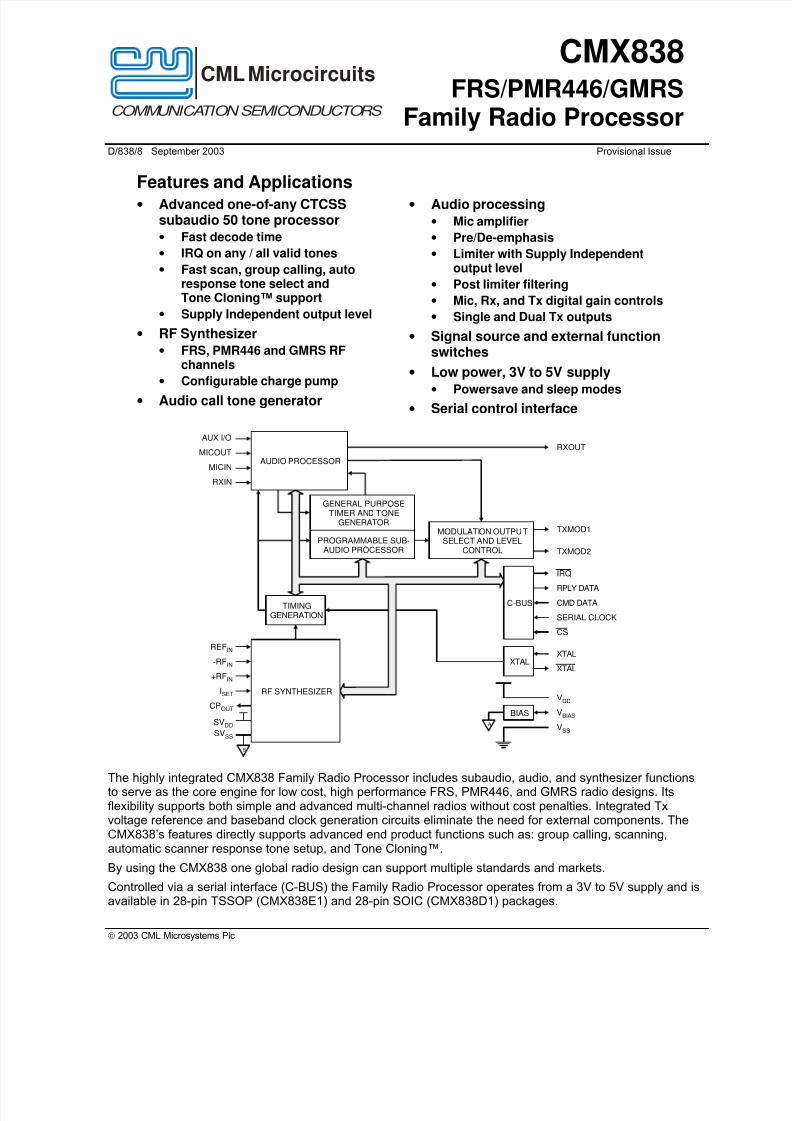
CML Microcircuits COMM UNICA TION SEMI CONDUCTO RS CMX838 FRS/PMR446/GMRS Family Radio Processor 2003 CML Microsystems Plc D/838/8 September 2003 Provisional Issue Features and Applications • Advanced one-of-any CTCSS subaudio 50 tone processor • Fast decode time • IRQ on any / all valid tones • Fast scan, group calling, auto response tone select and Tone Cloning™ support • Supply Independent output level • RF Synthesizer • FRS, PMR446 and GMRS RF channels • Configurable charge pump • Audio call tone generator • Audio processing • Mic amplifier • Pre/De-emphasis • Limiter with Supply Independent output level • Post limiter filtering • Mic, Rx, and Tx digital gain controls • Single and Dual Tx outputs • Signal source and external function switches • Low power, 3V to 5V supply • Powersave and sleep modes • Serial control interface MICIN RXIN RXOUT TXMOD1 XTAL AUX I/O C-BUS -RF IN +RF IN REF IN SV SS SV DD XTAL XTAL I SET CP OUT RF SYNTHESIZER S TXMOD2 MICOUT TIMING GENERATION IRQ RPLY DATA CMD DATA SERIAL CLOCK CS PROGRAMMABLE SUB- AUDIO PROCESSOR MODULATI ON OUTPUT SELECT AND LEVEL CONTROL AUDIO PROCESSOR BIAS V BIAS V SS V DD A GENERAL PURPOSE TIMER AND TONE GENERATOR The highly integrated CMX838 Family Radio Processor includes subaudio, audio, and synthesizer functions to serve as the core engine for low cost, high performance FRS, PMR446, and GMRS radio designs. Its flexibility supports both simple and advanced multi-channel radios without cost penalties. Integrated Tx voltage reference and baseband clock generation circuits eliminate the need for external components. The CMX838’s features directly supports advanced end product functions such as: group calling, scanning, automatic scanner response tone setup, and Tone Cloning™. By using the CMX838 one global radio design can support multiple standards and markets. Controlled via a serial interface (C-BUS) the Family Radio Processor operates from a 3V to 5V supply and is available in 28-pin TSSOP (CMX838E1) and 28-pin SOIC (CMX838D1) packages.
-
Upload
tombenson1234 -
Category
Documents
-
view
238 -
download
0
Transcript of Radio Gmrs Radio
7/29/2019 Radio Gmrs Radio
http://slidepdf.com/reader/full/radio-gmrs-radio 1/72
CML Microcircuits
COMMUNICATION SEMICONDUCTORS
CMX838FRS/PMR446/GMRS
Family Radio Processor
2003 CML Microsystems Plc
D/838/8 September 2003 Provisional Issue
Features and Applications• Advanced one-of-any CTCSS
subaudio 50 tone processor• Fast decode time
• IRQ on any / all valid tones
• Fast scan, group calling, autoresponse tone select andTone Cloning™ support
• Supply Independent output level
• RF Synthesizer• FRS, PMR446 and GMRS RF
channels
• Configurable charge pump
• Audio call tone generator
• Audio processing
• Mic amplifier
• Pre/De-emphasis
• Limiter with Supply Independentoutput level
• Post limiter filtering
• Mic, Rx, and Tx digital gain controls
• Single and Dual Tx outputs
• Signal source and external functionswitches
• Low power, 3V to 5V supply• Powersave and sleep modes
• Serial control interface
MICIN
RXIN
RXOUT
TXMOD1
XTAL
AUX I/O
C-BUS
-RFIN
+RFIN
REFIN
SVSS
SVDD
XTAL
XTAL
ISET
CPOUT
RF SYNTHESIZER
S
TXMOD2
MICOUT
TIMING
GENERATION
IRQ
RPLY DATA
CMD DATA
SERIAL CLOCK
CS
PROGRAMMABLE SUB-
AUDIO PROCESSOR
MODULATION OUTPUT
SELECT AND LEVEL
CONTROL
AUDIO PROCESSOR
BIAS VBIAS
VSS
VDD
A
GENERAL PURPOSE
TIMER AND TONE
GENERATOR
The highly integrated CMX838 Family Radio Processor includes subaudio, audio, and synthesizer functionsto serve as the core engine for low cost, high performance FRS, PMR446, and GMRS radio designs. Itsflexibility supports both simple and advanced multi-channel radios without cost penalties. Integrated Txvoltage reference and baseband clock generation circuits eliminate the need for external components. TheCMX838’s features directly supports advanced end product functions such as: group calling, scanning,automatic scanner response tone setup, and Tone Cloning™.
By using the CMX838 one global radio design can support multiple standards and markets.
Controlled via a serial interface (C-BUS) the Family Radio Processor operates from a 3V to 5V supply and isavailable in 28-pin TSSOP (CMX838E1) and 28-pin SOIC (CMX838D1) packages.
7/29/2019 Radio Gmrs Radio
http://slidepdf.com/reader/full/radio-gmrs-radio 2/72
FRS/PMR446/GMRS Family Radio Processor CMX838
2003 CML Microsystems Plc 2 D/838/8
CONTENTSSection Page
1 Block Diagram................................................................................................................6
2 Signal List.......................................................................................................................7
3 External Components....................................................................................................9
4 General Description.....................................................................................................10 4.1 Audio ............................................................................................................................... 10
4.1.1 Digitally Controlled Amplifiers (DCA).....................................................................................10
4.1.2 Transmit Input Amplifier ........................................................................................................11
4.1.3 Audio Switched Capacitor Filters ..........................................................................................11
4.1.3.1 Pre-emphasis/Low-pass Filter.........................................................................................12
4.1.3.2 High-pass Filter ...............................................................................................................13
4.1.3.3 Deviation Limiter Low-pass Filter....................................................................................13
4.1.4 De-emphasis .........................................................................................................................14
4.1.5 Transmit Audio Path..............................................................................................................14
4.1.6 Receive Audio Path...............................................................................................................15 4.1.7 Audio Path without De-emphasis or Pre-emphasis...............................................................15
4.1.8 Deviation Limiter....................................................................................................................16
4.2 Tone Signaling Processor................................................................................................ 17
4.2.1 Tone encoding/decoding .......................................................................................................17
4.2.2 Subaudio RX and TX Filter Characteristics...........................................................................18
4.2.3 CTCSS Subaudio Decoder and Encoder Tone Set ..............................................................20
4.2.4 Tone Signaling Processor Configuration Task Descriptions.................................................21
4.2.4.1 Normal Run Mode (Task 0).............................................................................................21
4.2.4.2 Reserved For Test (Task 1-3).........................................................................................21
4.2.4.3 RX Configuration.............................................................................................................22
4.2.4.4 TX Configuration .............................................................................................................23
4.2.4.5 Initialize and Configure....................................................................................................24
4.3 RF Synthesizer................................................................................................................ 26
4.3.1 Operating Range and Specifications.....................................................................................26
4.3.2 Main Divider...........................................................................................................................26
4.3.3 Phase Detector & Charge Pump...........................................................................................26
4.3.4 Lock Detect Output................................................................................................................27
4.3.5 Reference Circuits.................................................................................................................27
4.4 Baseband Timing Generation .......................................................................................... 27
5 Software Programming ...............................................................................................28
5.1 C-BUS Serial Interface .................................................................................................... 28
5.1.1 8-Bit C-BUS Register Map ....................................................................................................29
5.1.2 16-Bit C-BUS Register Map ..................................................................................................30
5.1.2.1 GENERAL RESET ($01).................................................................................................30
5.1.2.2 SETUP Register ($80) ....................................................................................................31
5.1.2.3 AUDIO CONTROL Register ($81) ..................................................................................32
5.1.2.4 RX AUDIO LEVEL CONTROL Register ($82)................................................................33

7/29/2019 Radio Gmrs Radio
http://slidepdf.com/reader/full/radio-gmrs-radio 3/72
FRS/PMR446/GMRS Family Radio Processor CMX838
2003 CML Microsystems Plc 3 D/838/8
5.1.2.5 AUDIO POWER AND BANDWIDTH CONTROL Register ($83) ....................................34
5.1.2.6 TXMOD 1 & 2 CONTROL Register ($88) .......................................................................35
5.1.2.7 SYNTHESIZER BASEBAND CLK CONTROL Register ($89)........................................37
5.1.2.8 SYNTHESIZER GENERAL CONTROL Register ($8A)..................................................38
5.1.2.9 SYNTHESIZER CHANNEL SELECT Register ($8B) .....................................................39
5.1.2.10 SYNTHESIZER STATUS Register ($8C) .......................................................................39
5.1.2.11 SYNTHESIZER 1ST IF OFFSET Register ($8D) ...........................................................40
5.1.2.12 16 BIT SUBAUDIO TASK DATA Register ($8E) ............................................................40
5.1.2.13 16 BIT SUBAUDIO TEST DATA Register ($8F).............................................................40
5.1.2.14 SYNTHESIZER TEST Register ($90).............................................................................40
5.1.2.15 16 BIT SUBAUDIO TEST READ DATA Register ($91)..................................................41
5.1.2.16 TONE SIGNALING CONTROL Register ($93)...............................................................41
5.1.2.17 SUBAUDIO STATUS Register ($94) ..............................................................................42
5.1.2.18 8 BIT SUBAUDIO TASK DATA Register ($95)...............................................................42
5.1.2.19 SUBAUDIO ANALOG CONTROL Register ($97)...........................................................43
6 Application Notes ........................................................................................................45
6.1 Overview ......................................................................................................................... 45 6.2 Basic FRS Radio Architecture ......................................................................................... 46
6.3 CMX838 Architectural Overview ...................................................................................... 47
6.4 Detailed CMX838 Architecture......................................................................................... 47
6.4.1 Audio Processing...................................................................................................................48
6.4.2 Tone Signaling Processor .....................................................................................................50
6.4.3 Level Control .........................................................................................................................52
6.4.4 Synthesizer and Charge Pump .............................................................................................54
6.4.5 Clock Generation...................................................................................................................54
6.4.6 Powersave Functions ............................................................................................................55
6.5 Control Registers Illustrated............................................................................................. 55
6.6 Application Examples ...................................................................................................... 58
6.6.1 CMX838 Initialization.............................................................................................................58
6.6.1.1 Register Descriptions: .....................................................................................................58
6.6.2 TX, subaudio encoding, single point modulation...................................................................58
6.6.2.1 Register Descriptions: .....................................................................................................59
6.6.3 RX, subaudio decode CTCSS tone or tones.........................................................................60
6.6.3.1 Register Descriptions: .....................................................................................................60
6.6.4 RX, multiple subaudio tone detect - Tone Cloning™ ............................................................62
6.6.4.1
Register Descriptions: .....................................................................................................62
7 Performance Specification..........................................................................................64
7.1 Electrical Performance..................................................................................................... 64
7.1.1 Absolute Maximum Ratings...................................................................................................64
7.1.2 Operating Limits ....................................................................................................................64
7.1.3 Operating Characteristics......................................................................................................65
7.1.4 Timing....................................................................................................................................68
7.2 Packaging........................................................................................................................ 70
7/29/2019 Radio Gmrs Radio
http://slidepdf.com/reader/full/radio-gmrs-radio 4/72
FRS/PMR446/GMRS Family Radio Processor CMX838
2003 CML Microsystems Plc 4 D/838/8
FIGURESFigure Page
Figure 1: Block Diagram......................................................................................................................................6
Figure 2: Recommended External Components.................................................................................................9
Figure 3: Audio Processing Block Diagram ......................................................................................................10
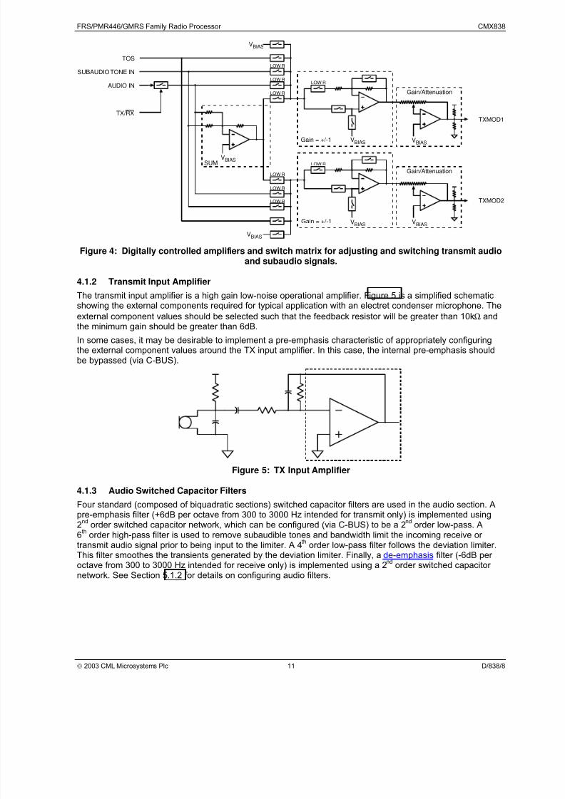
Figure 4: Digitally controlled amplifiers and switch matrix for adjusting and switching transmit audio and
subaudio signals. ...............................................................................................................................11 Figure 5: TX Input Amplifier ..............................................................................................................................11
Figure 6: Magnitude response for input low-pass filter. ....................................................................................12
Figure 7: Magnitude response for pre-emphasis filter. .....................................................................................12
Figure 8: Magnitude response of high-pass filter..............................................................................................13
Figure 9: Magnitude response of post-deviation limiter low-pass filter.............................................................13
Figure 10: Magnitude response of de-emphasis filter.......................................................................................14
Figure 11: Transmit audio path frequency response with pre-emphasis. .........................................................14
Figure 12: Receive audio path frequency response with de-emphasis. ...........................................................15
Figure 13: Audio path frequency response without pre-emphasis or de-emphasis..........................................15
Figure 14: Deviation limiter block diagram........................................................................................................16 Figure 15: Subaudio Block Diagram .................................................................................................................17
Figure 16: Subaudio RX filter gain for normal CTCSS operation. ....................................................................18
Figure 17: Subaudio RX filter delay for normal CTCSS operation....................................................................18
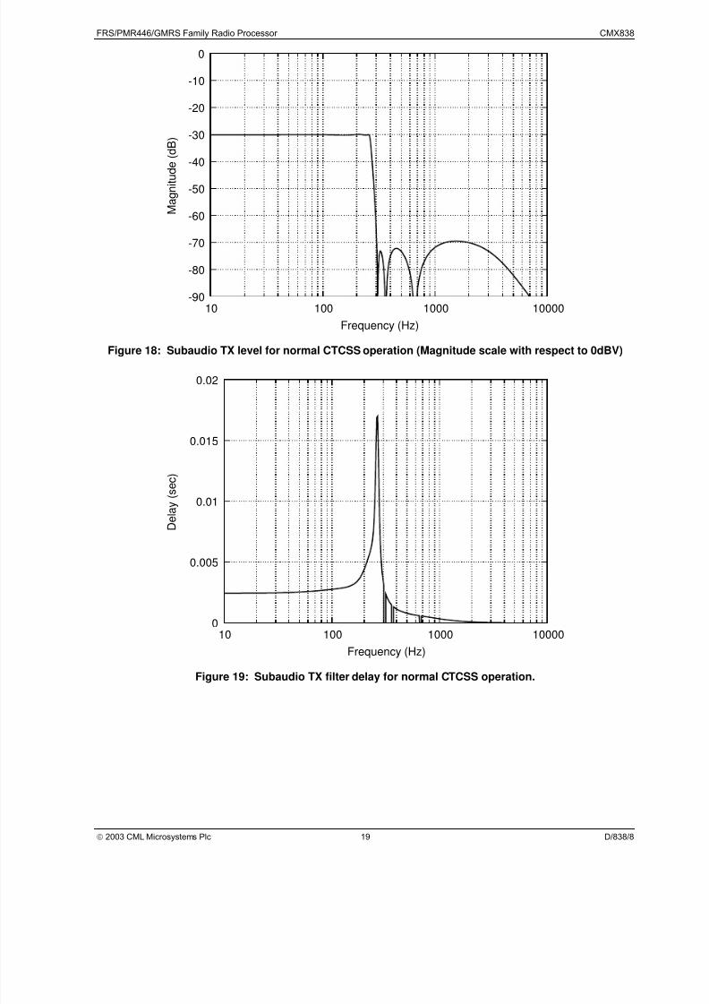
Figure 18: Subaudio TX level for normal CTCSS operation (Magnitude scale with respect to 0dBV) .............19
Figure 19: Subaudio TX filter delay for normal CTCSS operation. ...................................................................19
Figure 20: RF Synthesizer block diagram.........................................................................................................26
Figure 21: Block diagram of main programmable divider. ................................................................................26
Figure 22: C-BUS transaction timing diagram. .................................................................................................28
Figure 23: Basic FRS Radio Tx Architecture ....................................................................................................46
Figure 24: Basic FRS Radio Rx Architecture....................................................................................................46 Figure 25: CMX838 Main Function Blocks........................................................................................................47
Figure 26: CMX838 Main Sections ...................................................................................................................47
Figure 27: Audio Processing .............................................................................................................................48
Figure 28: Example Audio RX Path ..................................................................................................................49
Figure 29: Example Audio TX Voice Path.........................................................................................................49
Figure 30: Example Audio TX Internally Generated Tone with Loudspeaker Enabled Path............................49
Figure 31: Tone Signaling Processor................................................................................................................50
Figure 32: Example CTCSS Tone Decoder Path .............................................................................................51
Figure 33: Example CTCSS Tone Encoder Path .............................................................................................51
Figure 34: Example Internal Audio Tone Encoder Path ...................................................................................52
Figure 35: Level Control....................................................................................................................................52
Figure 36: Example Single Point Modulation Level Path..................................................................................53
Figure 37: Example Two-Point Modulation Level Paths ...................................................................................53
Figure 38: Example Single Point Modulation with Varied Subaudio Level Paths.............................................53
Figure 39: Synthesizer and Charge Pump........................................................................................................54
Figure 40: Clock Generation .............................................................................................................................54
Figure 41: Powersave Scope and Related Control Registers ..........................................................................55
Figure 42: Synthesizer to Baseband Clock Control, $89 ..................................................................................55
7/29/2019 Radio Gmrs Radio
http://slidepdf.com/reader/full/radio-gmrs-radio 5/72
FRS/PMR446/GMRS Family Radio Processor CMX838
2003 CML Microsystems Plc 5 D/838/8
Figure 43: Setup, $80........................................................................................................................................56
Figure 44: Audio ($81), RX Audio Level ($82) and Subaudio Analog ($97) Control ........................................56
Figure 45: Audio Power and Bandwidth Control, $83.......................................................................................57
Figure 46: TXMOD1 & TXMOD2 Control, $88..................................................................................................57
Figure 47: Application Example TX, Subaudio Encoding, Single Point Modulation .........................................60
Figure 48: C-BUS Timing ..................................................................................................................................69
Figure 49: 28-pin TSSOP (E1) Mechanical Outline: Order as part no. CMX838E1 ........................................70
Figure 50: 28-pin SOIC (D1) Mechanical Outline: Order as part no. CMX838D1 ...........................................70

7/29/2019 Radio Gmrs Radio
http://slidepdf.com/reader/full/radio-gmrs-radio 6/72
FRS/PMR446/GMRS Family Radio Processor CMX838
2003 CML Microsystems Plc 6 D/838/8
1 Block Diagram
CTCSSDECODERS
+
CTCSSENCODE
RXIN
BIAS
AUXI/O
C-BUS
Serial
Interface
DIVIDE32/33
PROGRAMMABLE
DIVIDER
12BITPROGRAMMABLE
REFERENCECO
UNTER
PHASE
DETECTOR
CHARGE
PUMP
LOCK
DETECT
+RFIN
-RFIN
REFIN
SVSS
SVDD
VBIAS
XTAL
XTAL
I SET
CPOUT
VSS
VDD
S
BASEBAND
TIMING
GENERATION
SERIALCLOCK
CS
LPF
VBIAS
VBIAS
VBIAS
AUDIO
TONEENCODE
0°/180°
phase
0°/180°
phase
CMD
DATA
RPLYDATA
IRQ
TXMOD1
TXMOD2
RXNOTONE/
TXDURATIONTIMER
VOLTAGEREF
BPF
MICIN
MICOUT
PRE
LPF
HPF
LPF
LIM
BIN
AIN
AOUT
BOUT
VBIAS
VOLTAGEREF
DEEMP
VOLTAGEREF
1 0
VBIAS
RXOUT
Figure 1: Block Diagram
7/29/2019 Radio Gmrs Radio
http://slidepdf.com/reader/full/radio-gmrs-radio 7/72
FRS/PMR446/GMRS Family Radio Processor CMX838
2003 CML Microsystems Plc 7 D/838/8
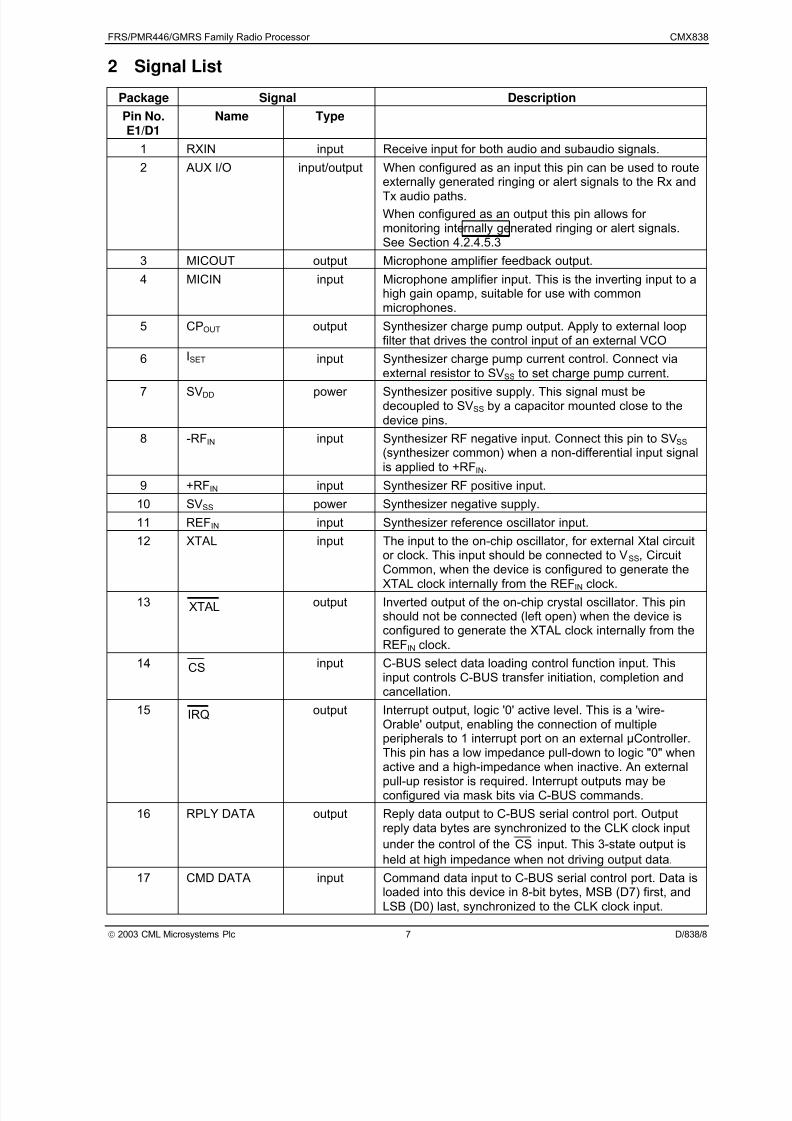
2 Signal List
Package Signal Description
Pin No.E1/D1
Name Type
1 RXIN input Receive input for both audio and subaudio signals.
2 AUX I/O input/output When configured as an input this pin can be used to routeexternally generated ringing or alert signals to the Rx andTx audio paths.
When configured as an output this pin allows for monitoring internally generated ringing or alert signals.See Section 4.2.4.5.3
3 MICOUT output Microphone amplifier feedback output.
4 MICIN input Microphone amplifier input. This is the inverting input to ahigh gain opamp, suitable for use with commonmicrophones.
5 CPOUT output Synthesizer charge pump output. Apply to external loopfilter that drives the control input of an external VCO
6 ISET input Synthesizer charge pump current control. Connect via
external resistor to SVSS to set charge pump current.7 SVDD power Synthesizer positive supply. This signal must be
decoupled to SVSS by a capacitor mounted close to thedevice pins.
8 -RFIN input Synthesizer RF negative input. Connect this pin to SVSS (synthesizer common) when a non-differential input signalis applied to +RFIN.
9 +RFIN input Synthesizer RF positive input.
10 SVSS power Synthesizer negative supply.
11 REFIN input Synthesizer reference oscillator input.
12 XTAL input The input to the on-chip oscillator, for external Xtal circuitor clock. This input should be connected to VSS, Circuit
Common, when the device is configured to generate theXTAL clock internally from the REFIN clock.
13 XTAL output Inverted output of the on-chip crystal oscillator. This pinshould not be connected (left open) when the device isconfigured to generate the XTAL clock internally from theREFIN clock.
14 CS input C-BUS select data loading control function input. Thisinput controls C-BUS transfer initiation, completion andcancellation.
15 IRQ output Interrupt output, logic '0' active level. This is a 'wire-Orable' output, enabling the connection of multipleperipherals to 1 interrupt port on an external µController.
This pin has a low impedance pull-down to logic "0" whenactive and a high-impedance when inactive. An externalpull-up resistor is required. Interrupt outputs may beconfigured via mask bits via C-BUS commands.
16 RPLY DATA output Reply data output to C-BUS serial control port. Outputreply data bytes are synchronized to the CLK clock input
under the control of the CS input. This 3-state output is
held at high impedance when not driving output data.
17 CMD DATA input Command data input to C-BUS serial control port. Data isloaded into this device in 8-bit bytes, MSB (D7) first, andLSB (D0) last, synchronized to the CLK clock input.
7/29/2019 Radio Gmrs Radio
http://slidepdf.com/reader/full/radio-gmrs-radio 8/72
FRS/PMR446/GMRS Family Radio Processor CMX838
2003 CML Microsystems Plc 8 D/838/8
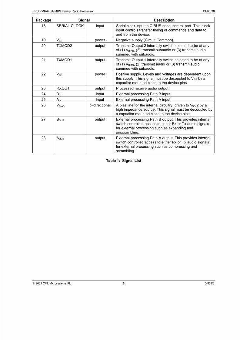
Package Signal Description
18 SERIAL CLOCK input Serial clock input to C-BUS serial control port. This clockinput controls transfer timing of commands and data toand from the device.
19 VSS power Negative supply (Circuit Common)
20 TXMOD2 output Transmit Output 2 internally switch selected to be at anyof (1) VBIAS, (2) transmit subaudio or (3) transmit audiosummed with subaudio.
21 TXMOD1 output Transmit Output 1 internally switch selected to be at anyof (1) VBIAS, (2) transmit audio or (3) transmit audiosummed with subaudio.
22 VDD power Positive supply. Levels and voltages are dependent uponthis supply. This signal must be decoupled to VSS by acapacitor mounted close to the device pins.
23 RXOUT output Processed receive audio output.
24 BIN input External processing Path B input.
25 AIN input External processing Path A input.
26 VBIAS bi-directional A bias line for the internal circuitry, driven to VDD/2 by ahigh impedance source. This signal must be decoupled by
a capacitor mounted close to the device pins.27 BOUT output External processing Path B output. This provides internal
switch controlled access to either Rx or Tx audio signalsfor external processing such as expanding andunscrambling.
28 AOUT output External processing Path A output. This provides internalswitch controlled access to either Rx or Tx audio signalsfor external processing such as compressing andscrambling.
Table 1: Signal List
7/29/2019 Radio Gmrs Radio
http://slidepdf.com/reader/full/radio-gmrs-radio 9/72
FRS/PMR446/GMRS Family Radio Processor CMX838
2003 CML Microsystems Plc 9 D/838/8
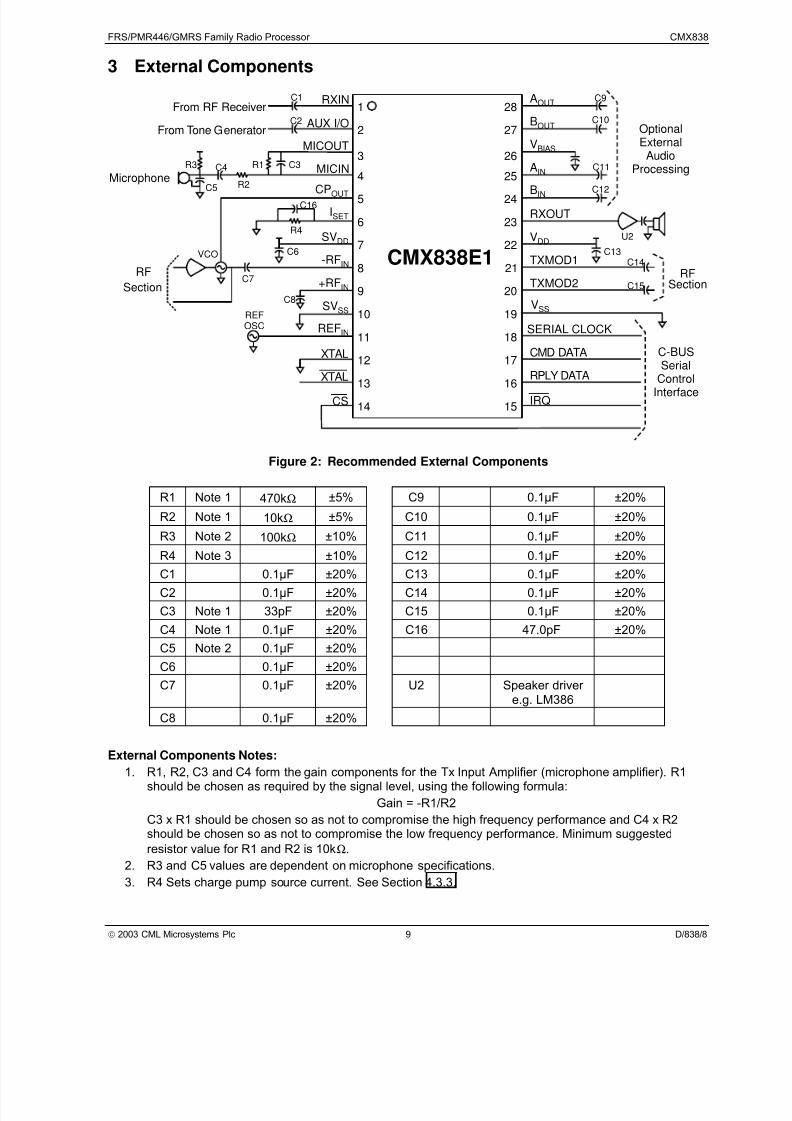
3 External Components
AOUT
BOUT
VBIAS
AIN
BIN
RXOUT
VDD
TXMOD1
TXMOD2
RXIN
IRQ
RPLY DATA
CMD DATA
SERIAL CLOCK
VSS
CMX838E1
AUX I/O
MICOUT
MICIN
CPOUT
ISET
SVDD
REFIN
-RFIN
+RFIN
SVSS
XTAL
XTAL
CS
C-BUSSerial
ControlInterface
C1
C2
C3C4
C5
C6
C7
C8
C15
C14C13
C12
C11
C10
C9
U2
RF
Section
REFOSC
VCO
From RF Receiver
From Tone Generator
Microphone
RFSection
R1
R2
R4
R3
1
2
3
4
5
6
7
8
9
10
11
12
13
14
28
27
26
25
24
23
22
21
20
19
18
17
16
15
C16
OptionalExternal
AudioProcessing
Figure 2: Recommended External Components
R1 Note 1 470kΩ ±5% C9 0.1µF ±20%
R2 Note 1 10kΩ ±5% C10 0.1µF ±20%
R3 Note 2 100kΩ ±10% C11 0.1µF ±20%
R4 Note 3 ±10% C12 0.1µF ±20%
C1 0.1µF ±20% C13 0.1µF ±20%
C2 0.1µF ±20% C14 0.1µF ±20%
C3 Note 1 33pF ±20% C15 0.1µF ±20%
C4 Note 1 0.1µF ±20% C16 47.0pF ±20%
C5 Note 2 0.1µF ±20%
C6 0.1µF ±20%
C7 0.1µF ±20% U2 Speaker driver e.g. LM386
C8 0.1µF ±20%
External Components Notes:1. R1, R2, C3 and C4 form the gain components for the Tx Input Amplifier (microphone amplifier). R1
should be chosen as required by the signal level, using the following formula:
Gain = -R1/R2
C3 x R1 should be chosen so as not to compromise the high frequency performance and C4 x R2should be chosen so as not to compromise the low frequency performance. Minimum suggestedresistor value for R1 and R2 is 10kΩ.
2. R3 and C5 values are dependent on microphone specifications.
3. R4 Sets charge pump source current. See Section 4.3.3.
7/29/2019 Radio Gmrs Radio
http://slidepdf.com/reader/full/radio-gmrs-radio 10/72
FRS/PMR446/GMRS Family Radio Processor CMX838
2003 CML Microsystems Plc 10 D/838/8
4 General Description
4.1 Audio
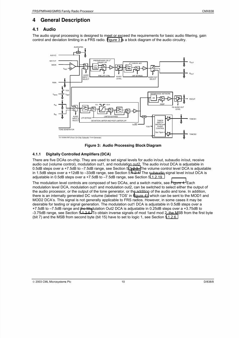
The audio signal processing is designed to meet or exceed the requirements for basic audio filtering, gaincontrol and deviation limiting in a FRS radio. Figure 3 is a block diagram of the audio circuitry.
RXIN
TX SUBAUDIO (From On-Chip Subaudio Tone Generator)
RXOUT
AUX I/O
MICIN
MICOUT
VREF
LP
PRE 11
1
DE1
TXMOD1
AOUT
BOUT
AIN
BIN
DEEMPHASIS NETWORK
DEVIATION LIMITER AND POST-LIMITER LPF
PREEMPHASIS OR 2ORDER LPF
ND
6 ORDER HPFTH
LPF BYPASSLIMITER BYPASS
AUDIOINPUT 1SELECT
AUDIO OUTSELECT
PRE LPF CTRL HPF BYPASS
DEBP
RX AUDIO OUTLEVEL
AUDIOLEVEL
VREFVBIAS
TOS
VLHVLL
TOS
TXMOD2
TX/RX
TONE GENERATOR
AUXPUPEN
AUDIOINPUT 2SELECT TXMOD
SWITCHMATRIX and
PHASECONTROL
See Figure 4
Figure 3: Audio Processing Block Diagram
4.1.1 Digitally Controlled Amplifiers (DCA)
There are five DCAs on-chip. They are used to set signal levels for audio in/out, subaudio in/out, receiveaudio out (volume control), modulation out1, and modulation out2. The audio in/out DCA is adjustable in0.5dB steps over a +7.5dB to –7.5dB range, see Section 5 .1.2.3.
The volume control level DCA is adjustable
in 1.5dB steps over a +12dB to –33dB range, see Section 5.1.2.4. The s ubaudio signal level in/out DCA isadjustable in 0.5dB steps over a +7.5dB to –7.5dB range, see Section 5 .1.2.19
The modulation level controls are composed of two DCAs, and a switch matrix, see Figure 4. Eachmodulation level DCA, modulation out1 and modulation out2, can be switched to select either the output of the audio processor, or the output of the tone generator, or the addition of the audio and tone. In addition,there is an internally generated DC volume (labeled ‘TOS’ in Figure 4), which can be sent to the MOD1 andMOD2 DCA’s. This signal is not generally applicable to FRS radios. However, in some cases it may bedesirable for testing or signal generation. The modulation out1 DCA is adjustable in 0.5dB steps over a+7.5dB to –7.5dB range and the Modulation Out2 DCA is adjustable in 0.25dB steps over a +3.75dB to-3.75dB range, see Section 5.1.2.6. To obtain inverse signals of mod 1and mod 2, the MSB from the first byte(bit 7) and the MSB from second byte (bit 15) have to set to logic 1, see Section 5.1.2.6.
7/29/2019 Radio Gmrs Radio
http://slidepdf.com/reader/full/radio-gmrs-radio 11/72
FRS/PMR446/GMRS Family Radio Processor CMX838
2003 CML Microsystems Plc 11 D/838/8
TXMOD1
TXMOD2
VBIAS
VBIAS
VBIAS
VBIAS
VBIAS
VBIAS
TOS
SUBAUDIO TONE IN
LOW R
LOW R
LOW R
LOW R
LOW R
LOW R
LOW R
LOW R
SUM
Gain/Attenuation
Gain = +/-1
TX/RX
VBIAS
Gain/Attenuation
Gain = +/-1
AUDIO IN
Figure 4: Digitally controlled amplifiers and switch matrix for adjusting and switching transmit audioand subaudio signals.
4.1.2 Transmit Input Amplifier
The transmit input amplifier is a high gain low-noise operational amplifier. Figure 5 is a simplified schematicshowing the external components required for typical application with an electret condenser microphone. Theexternal component values should be selected such that the feedback resistor will be greater than 10kΩ andthe minimum gain should be greater than 6dB.
In some cases, it may be desirable to implement a pre-emphasis characteristic of appropriately configuringthe external component values around the TX input amplifier. In this case, the internal pre-emphasis shouldbe bypassed (via C-BUS).
Figure 5: TX Input Amplifier
4.1.3 Audio Switched Capacitor Filters
Four standard (composed of biquadratic sections) switched capacitor filters are used in the audio section. Apre-emphasis filter (+6dB per octave from 300 to 3000 Hz intended for transmit only) is implemented using2nd order switched capacitor network, which can be configured (via C-BUS) to be a 2nd order low-pass. A
6
th
order high-pass filter is used to remove subaudible tones and bandwidth limit the incoming receive or transmit audio signal prior to being input to the limiter. A 4 th order low-pass filter follows the deviation limiter.This filter smoothes the transients generated by the deviation limiter. Finally, a de-emphasis filter (-6dB per octave from 300 to 3000 Hz intended for receive only) is implemented using a 2nd order switched capacitor network. See Section 5.1.2 f or details on configuring audio filters.

7/29/2019 Radio Gmrs Radio
http://slidepdf.com/reader/full/radio-gmrs-radio 12/72
FRS/PMR446/GMRS Family Radio Processor CMX838
2003 CML Microsystems Plc 12 D/838/8
4.1.3.1 Pre-emphasis/Low-pass Filter
Figure 6 shows magnitude response for the Input Pre-emphasis/Low-pass Filter when programmed for low-pass mode. This mode would typically be selected when processing Rx audio.
-35
-30
-25
-20
-15
-10
-5
0
5
1000 10000
M a g n i t u d e ( d B )
Frequency (Hz)
Figure 6: Magnitude response for input low-pass filter.
Figure 7 shows magnitude response for the Input Pre-emphasis/Low-pass Filter when programmed for Pre-emphasis mode. This mode would typically be selected when processing Tx audio.
-20
-15
-10
-5
0
5
10
15
100 1000 10000
M a g n i t u d e ( d B )
Frequency (Hz)
Figure 7: Magnitude response for pre-emphasis filter.

7/29/2019 Radio Gmrs Radio
http://slidepdf.com/reader/full/radio-gmrs-radio 13/72
FRS/PMR446/GMRS Family Radio Processor CMX838
2003 CML Microsystems Plc 13 D/838/8
4.1.3.2 High-pass Filter
Figure 8 shows the magnitude response for the Audio High Pass Filter. This filter’s purpose is to suppresssubaudio tones when processing both Rx and Tx audio.
-80
-70
-60
-50
-40
-30
-20
-10
0
10
10 100 1000 10000
M a g n i t u d e ( d B )
Frequency (Hz)
Figure 8: Magnitude response of high-pass filter.
4.1.3.3 Deviation Limiter Low-pass Filter
The magnitude response for narrowband and wideband modes is shown in F igure 9. Narrow-band mode isgenerally required for transmitting in systems having RF Channel BW ≤12.5kHz (e.g. FRS).
-40
-35
-30
-25
-20
-15
-10
-5
0
5
1000 10000
M a g n i t u d e ( d B )
Frequency (Hz)
WIDE BAND
NARROW BAND
Figure 9: Magnitude response of post-deviation limiter low-pass filter.

7/29/2019 Radio Gmrs Radio
http://slidepdf.com/reader/full/radio-gmrs-radio 14/72
FRS/PMR446/GMRS Family Radio Processor CMX838
2003 CML Microsystems Plc 14 D/838/8
4.1.4 De-emphasis
Figure 10 shows magnitude response for the De-emphasis Filter. This filter precedes the Rx Audio LevelControl and is generally required to process Rx audio.
-20
-15
-10
-5
0
5
10
15
100 1000 10000
M a g n i t u d e ( d B )
Frequency (Hz)
Figure 10: Magnitude response of de-emphasis filter.
4.1.5 Transmit Audio Path
Overall magnitude r esponse for the transmit audio path for wideband and narrowband with pre-emphasis isshown in Figure 11.
-80
-60
-40
-20
0
20
100 1000 10000
M a g n i t u d e ( d B )
Frequency (Hz)
NARROW BAND
WIDE BAND
Figure 11: Transmit audio path frequency response with pre-emphasis.
7/29/2019 Radio Gmrs Radio
http://slidepdf.com/reader/full/radio-gmrs-radio 15/72
FRS/PMR446/GMRS Family Radio Processor CMX838
2003 CML Microsystems Plc 15 D/838/8
4.1.6 Receive Audio Path
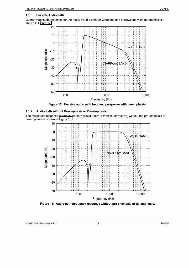
Overall magnitude response for the receive audio path for wideband and narrowband with de-emphasis isshown in Figure 12.
-60
-50
-40
-30
-20
-10
0
10
20
100 1000 10000
M a g n i t u d e ( d B )
Frequency (Hz)
NARROW BAND
WIDE BAND
Figure 12: Receive audio path frequency response with de-emphasis.
4.1.7 Audio Path without De-emphasis or Pre-emphasis
The magnitude response f or the audio path (could apply to transmit or receive) without the pre-emphasis or de-emphasis is shown in Figure 13.
-70
-60
-50
-40
-30
-20
-10
0
10
100 1000 10000
M a g n i t u d e ( d B )
Frequency (Hz)
NARROW BAND
WIDE BAND
Figure 13: Audio path frequency response without pre-emphasis or de-emphasis.

7/29/2019 Radio Gmrs Radio
http://slidepdf.com/reader/full/radio-gmrs-radio 16/72
FRS/PMR446/GMRS Family Radio Processor CMX838
2003 CML Microsystems Plc 16 D/838/8
4.1.8 Deviation Limiter
The purpose of the deviation limiter is to limit the signal level at baseband prior to reaching the RF modulator.This is necessary to avoid co-channel interference as well as conform to the spectral constraints stipulated byregulatory agencies (e.g. FCC). Figure 14 is a block diagram of the limiter circuitry. Applying a DC voltagebetween VDD and VDD/2 to the reference input sets the maximum peak-to-peak signal level. This reference isinternally set so the maximum signal level is 2.196VP-P and is constant over supply voltage.
-1
REFI N
TX AUDIOLIMITED SPEECH TO
POST DEVIATIONLIMITER FILTER
Figure 14: Deviation limiter block diagram.
7/29/2019 Radio Gmrs Radio
http://slidepdf.com/reader/full/radio-gmrs-radio 17/72
FRS/PMR446/GMRS Family Radio Processor CMX838
2003 CML Microsystems Plc 17 D/838/8
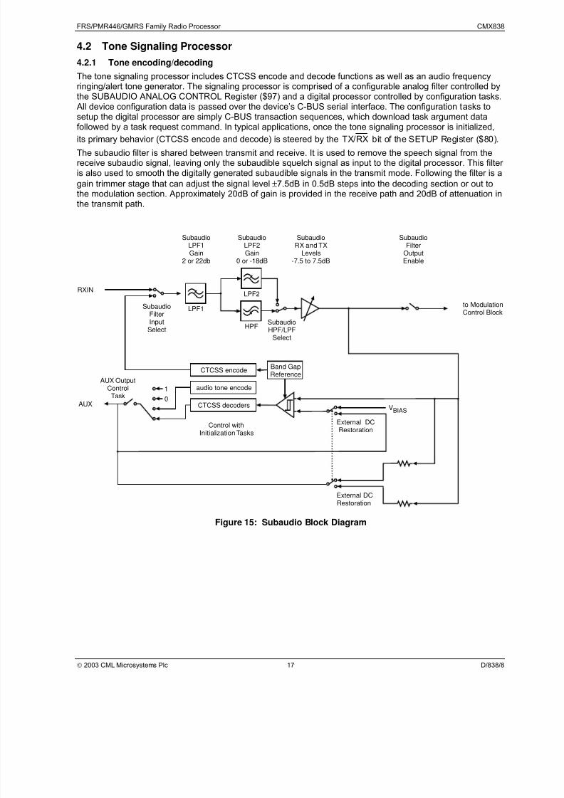
4.2 Tone Signaling Processor
4.2.1 Tone encoding/decoding
The tone signaling processor includes CTCSS encode and decode functions as well as an audio frequencyringing/alert tone generator. The signaling processor is comprised of a configurable analog filter controlled bythe SUBAUDIO ANALOG CONTROL Register ($97) and a digital processor controlled by configuration tasks. All device configuration data is passed over the device’s C-BUS serial interface. The configuration tasks tosetup the digital processor are simply C-BUS transaction sequences, which download task argument datafollowed by a task request command. In typical applications, once the tone signaling processor is initialized,
its primary behavior (CTCSS encode and decode) is steered by the RXTX/ bit of the SETUP Register ($80).
The subaudio filter is shared between transmit and receive. It is used to remove the speech signal from thereceive subaudio signal, leaving only the subaudible squelch signal as input to the digital processor. This filter is also used to smooth the digitally generated subaudible signals in the transmit mode. Following the filter is again trimmer stage that can adjust the signal level ±7.5dB in 0.5dB steps into the decoding section or out tothe modulation section. Approximately 20dB of gain is provided in the receive path and 20dB of attenuation inthe transmit path.
LPF1
CTCSS encode
CTCSS decoders
Band GapReference
audio tone encode
VBIAS
0
1
RXIN
to ModulationControl Block
AUX
AUX OutputControl
Task
External DCRestoration
SubaudioFilterInputSelect
SubaudioHPF/LPF
Select
SubaudioFilter
OutputEnable
SubaudioLPF1Gain
2 or 22db
HPF
LPF2
SubaudioRX and TX
Levels-7.5 to 7.5dB
External DCRestoration
Control withInitializationTasks
SubaudioLPF2Gain
0 or -18dB
Figure 15: Subaudio Block Diagram
7/29/2019 Radio Gmrs Radio
http://slidepdf.com/reader/full/radio-gmrs-radio 18/72
FRS/PMR446/GMRS Family Radio Processor CMX838
2003 CML Microsystems Plc 18 D/838/8
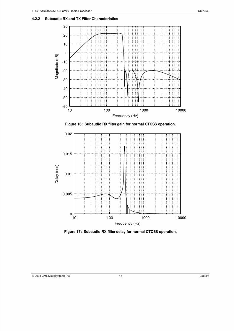
4.2.2 Subaudio RX and TX Filter Characteristics
-60
-50
-40
-30
-20
-10
0
10
20
30
10 100 1000 10000
M a g n i t u d e ( d B )
Frequency (Hz)
Figure 16: Subaudio RX filter gain for normal CTCSS operation.
0
0.005
0.01
0.015
0.02
10 100 1000 10000
D e l a y ( s e c
)
Frequency (Hz)
Figure 17: Subaudio RX filter delay for normal CTCSS operation.
7/29/2019 Radio Gmrs Radio
http://slidepdf.com/reader/full/radio-gmrs-radio 19/72
FRS/PMR446/GMRS Family Radio Processor CMX838
2003 CML Microsystems Plc 19 D/838/8
-90
-80
-70
-60
-50
-40
-30
-20
-10
0
10 100 1000 10000
M a g n i t u d e ( d B )
Frequency (Hz)
Figure 18: Subaudio TX level for normal CTCSS operation (Magnitude scale with respect to 0dBV)
0
0.005
0.01
0.015
0.02
10 100 1000 10000
D e l a y
( s e c )
Frequency (Hz)
Figure 19: Subaudio TX filter delay for normal CTCSS operation.
7/29/2019 Radio Gmrs Radio
http://slidepdf.com/reader/full/radio-gmrs-radio 20/72
FRS/PMR446/GMRS Family Radio Processor CMX838
2003 CML Microsystems Plc 20 D/838/8
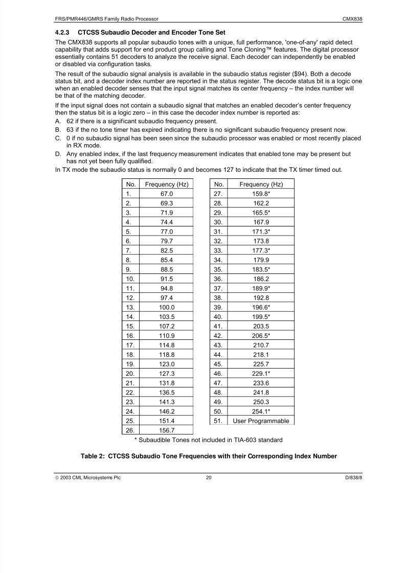
4.2.3 CTCSS Subaudio Decoder and Encoder Tone Set
The CMX838 supports all popular subaudio tones with a unique, full performance, 'one-of-any' rapid detectcapability that adds support for end product group calling and Tone Cloning™ features. The digital processor essentially contains 51 decoders to analyze the receive signal. Each decoder can independently be enabledor disabled via configuration tasks.
The result of the subaudio signal analysis is available in the subaudio status register ($94). Both a decodestatus bit, and a decoder index number are reported in the status register. The decode status bit is a logic onewhen an enabled decoder senses that the input signal matches its center frequency – the index number will
be that of the matching decoder.If the input signal does not contain a subaudio signal that matches an enabled decoder’s center frequencythen the status bit is a logic zero – in this case the decoder index number is reported as:
A. 62 if there is a significant subaudio frequency present.
B. 63 if the no tone timer has expired indicating there is no significant subaudio frequency present now.
C. 0 if no subaudio signal has been seen since the subaudio processor was enabled or most recently placedin RX mode.
D. Any enabled index, if the last frequency measurement indicates that enabled tone may be present buthas not yet been fully qualified.
In TX mode the subaudio status is normally 0 and becomes 127 to indicate that the TX timer timed out.
No. Frequency (Hz) No. Frequency (Hz)
1. 67.0 27. 159.8*2. 69.3 28. 162.2
3. 71.9 29. 165.5*
4. 74.4 30. 167.9
5. 77.0 31. 171.3*
6. 79.7 32. 173.8
7. 82.5 33. 177.3*
8. 85.4 34. 179.9
9. 88.5 35. 183.5*
10. 91.5 36. 186.2
11. 94.8 37. 189.9*12. 97.4 38. 192.8
13. 100.0 39. 196.6*
14. 103.5 40. 199.5*
15. 107.2 41. 203.5
16. 110.9 42. 206.5*
17. 114.8 43. 210.7
18. 118.8 44. 218.1
19. 123.0 45. 225.7
20. 127.3 46. 229.1*
21. 131.8 47. 233.622. 136.5 48. 241.8
23. 141.3 49. 250.3
24. 146.2 50. 254.1*
25. 151.4 51. User Programmable
26. 156.7
* Subaudible Tones not included in TIA-603 standard
Table 2: CTCSS Subaudio Tone Frequencies with their Corresponding Index Number
7/29/2019 Radio Gmrs Radio
http://slidepdf.com/reader/full/radio-gmrs-radio 21/72
FRS/PMR446/GMRS Family Radio Processor CMX838
2003 CML Microsystems Plc 21 D/838/8
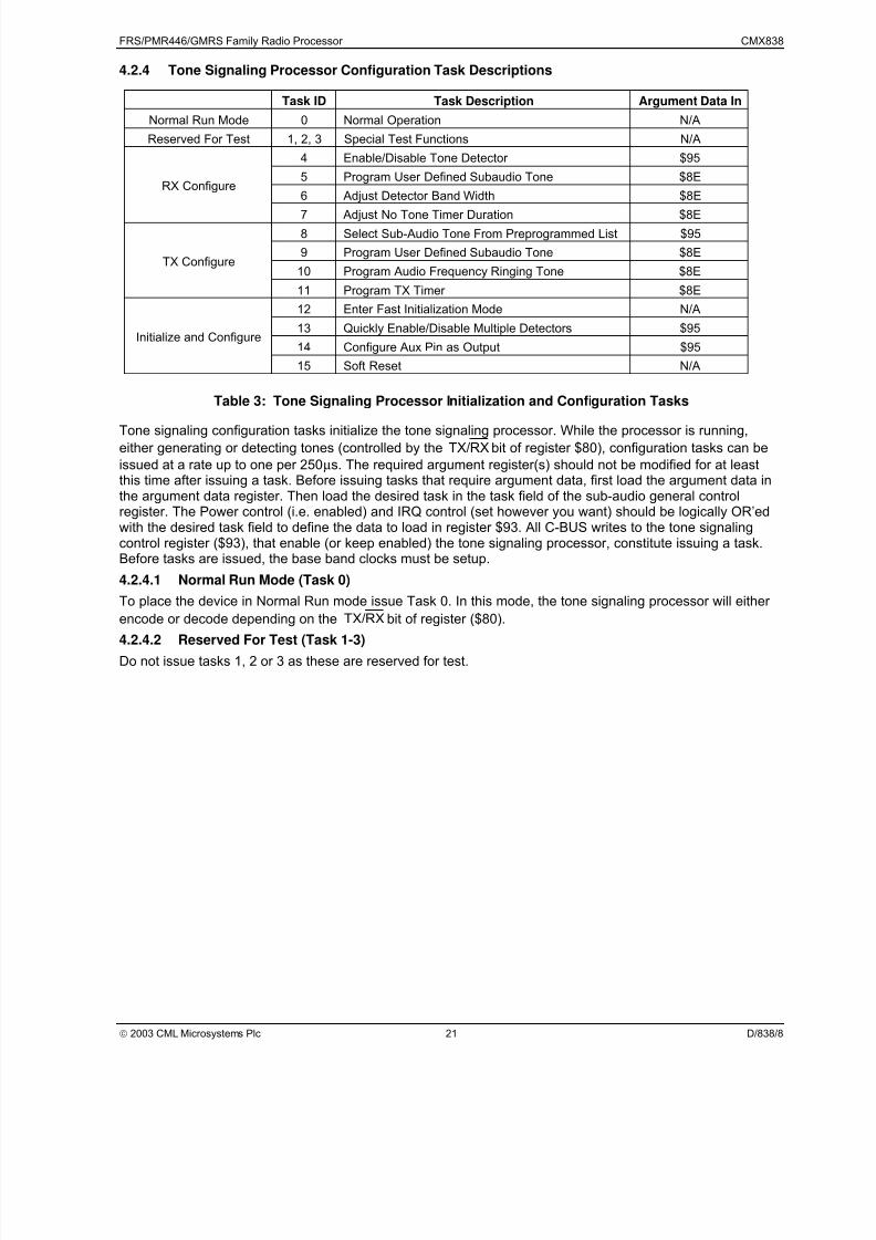
4.2.4 Tone Signaling Processor Configuration Task Descriptions
Task ID Task Description Argument Data In
Normal Run Mode 0 Normal Operation N/A
Reserved For Test 1, 2, 3 Special Test Functions N/A
4 Enable/Disable Tone Detector $95
5 Program User Defined Subaudio Tone $8E
6 Adjust Detector Band Width $8ERX Configure
7 Adjust No Tone Timer Duration $8E
8 Select Sub-Audio Tone From Preprogrammed List $95
9 Program User Defined Subaudio Tone $8E
10 Program Audio Frequency Ringing Tone $8ETX Configure
11 Program TX Timer $8E
12 Enter Fast Initialization Mode N/A
13 Quickly Enable/Disable Multiple Detectors $95
14 Configure Aux Pin as Output $95Initialize and Configure
15 Soft Reset N/A
Table 3: Tone Signaling Processor Initialization and Configuration Tasks
Tone signaling configuration tasks initialize the tone signaling processor. While the processor is running,
either generating or detecting tones (controlled by the RXTX/ bit of register $80), configuration tasks can beissued at a rate up to one per 250µs. The required argument register(s) should not be modified for at leastthis time after issuing a task. Before issuing tasks that require argument data, first load the argument data inthe argument data register. Then load the desired task in the task field of the sub-audio general controlregister. The Power control (i.e. enabled) and IRQ control (set however you want) should be logically OR’edwith the desired task field to define the data to load in register $93. All C-BUS writes to the tone signalingcontrol register ($93), that enable (or keep enabled) the tone signaling processor, constitute issuing a task.Before tasks are issued, the base band clocks must be setup.
4.2.4.1 Normal Run Mode (Task 0)
To place the device in Normal Run mode issue Task 0. In this mode, the tone signaling processor will either
encode or decode depending on the RXTX/ bit of register ($80).4.2.4.2 Reserved For Test (Task 1-3)
Do not issue tasks 1, 2 or 3 as these are reserved for test.
7/29/2019 Radio Gmrs Radio
http://slidepdf.com/reader/full/radio-gmrs-radio 22/72
FRS/PMR446/GMRS Family Radio Processor CMX838
2003 CML Microsystems Plc 22 D/838/8
4.2.4.3 RX Configuration
The following four tasks are used to control the decode behavior.
4.2.4.3.1 Enable or Disable Tone Detector (Task 4)
This task can be used to enable or disable tone detectors 1 to 51. Tone Detectors 1 to 50 have presetdetection center frequencies while tone detector 51 has a user programmable center frequency. This taskmay be issued multiple times to configure a tone watch list. It is recommended not to include non TIA-603tones with their adjacent TIA tones in a watch list.
Load argument in register $95, then issue task 4. Repeat as needed to configure tone watch list.The argument data has the following format in the 8 bit task data register ($95).
Bit 7 Bit 6 Bits 5-0
1=enable0=disable
Don’tcare
Tone detector index number (1-51)
Additionally using index 63 can enable or disable all detectors while issuing justone task. Enabling index 62 enables detection of all TIA-603 Tones. There is nosingle command to disable just the TIA-603 Tone Detectors – instead use index 63to disable all detectors.
For example to enable the 67Hz Tone Detector:
$95 0x81 // data to enable tone index 1 (67Hz)
$93 0x64 // task command to actually enable tone detector (and IRQ’s)4.2.4.3.2 Program User Defined RX Sub-Audio Tone (Task 5)
This task is used to program the center frequency of user programmable detector 51. Load the Argumentvalue in register $8E, then issue task 5.
The argument can be calculated according to the following equations.
R N Argument
f
N INT R
f INT N
+⋅=
⋅
⋅−+=
⋅⋅=
64
96
1000005115.0
100000
51196
The argument data for 65 Hz would be 31*64+14 = 0x07CEThe programmed center frequency can be back calculated by:
)511(96
100000
R
N f
−
⋅=
In the example above the actual center frequency would be 64.97 Hz.
A C-BUS sequence to setup tone detector 51 for 65Hz and enable just it would be:
$8E 0x07CE // Argument data for user defined 65Hz RX Tone.$93 0x45 // Task 5 command (No IRQ’s enabled)
wait 250µs
$95 0x3F // Task 4 argument data to disable all decoders
$93 0x44 // Task 4 command (No IRQ’s enabled)wait 250µs
$95 0xB3 // Task 4 argument data to enable decoder 51 (The user definable one)$93 0x64 // Task 4 command (with IRQ’s enabled)
wait 250µs
$93 0x60 // Task 0 command (to place device normal run mode with IRQ’s enabled)// last command is not required if the device was already in normal run mode
7/29/2019 Radio Gmrs Radio
http://slidepdf.com/reader/full/radio-gmrs-radio 23/72
FRS/PMR446/GMRS Family Radio Processor CMX838
2003 CML Microsystems Plc 23 D/838/8
4.2.4.3.3 Adjust Detector Band Width (Task 6)
The default bandwidth can be increased or decreased in increments of approximately 0.2% by loading a smallpositive or negative (2’s complement) value in register $8E and then issuing task 6. For the standard TIA toneset the default BW setting is recommended – so there is no need to adjust it. By default, the detector has asmall BW hysteresis to minimize chatter in marginal conditions.
4.2.4.3.4 Adjust No Tone Timer Duration (Task 7)
The default no tone timer duration can be increased or decreased in increments of 60µs by loading a positiveor negative (2’s complement) value in register $8E and then issuing task 7.
( )TimerDelta INT Argument ⋅+= 667.165.0
Where TimerDelta is the amount by which you want to increase or decrease the Default No Tone Timer inmilliseconds.
For example, to increase the default no tone timer by 10ms, load 167 (0xA7) into register $8E before issuingtask 7.
$8E 0x00A7$93 0x67 // Task 7 command to adjust no tone timer with IRQ’s enabled
4.2.4.4 TX Configuration
4.2.4.4.1 Select Sub-Audio Tone From Preprogrammed List (Task 8)
To select a preprogrammed sub-audio tone, load the index argument (1 to 50) in register $95 then issue
task 8.For example to set up TX tone to 114.8 Hz, the required C-BUS sequence would be
$95 0x11$93 0x48
4.2.4.4.2 Program User Defined TX Sub-Audio Tone (Task 9)
To program a user defined sub-audio tone, load the argument in register $8E then issue task 9. Where theargument is defined by,
⋅⋅+=
100000
65536365.0
f INT Argument
For example to set up TX tone to 65 Hz, the required C-BUS sequence would be
$8E 0x05FE
$93 0x49
4.2.4.4.3 Program Audio Frequency Ringing Tone (Task 10)
To program a user-defined audio ringing tone, load the argument in register $8E then issue task 10. Wherethe argument is defined by,
⋅⋅+=
100000
6553665.0
f INT Argument
For example to set up the ringing tone frequency to 620 Hz, the required C-BUS sequence would be
$8E 0x0986$93 0x4A
4.2.4.4.4 Program TX Timer (Task 11)
Load the argument in register $8E, then issue task 11. Where the argument is defined by, the number of 4mstime units,
⋅+=
− 3104
5.0T
INT Argument
For example, to set up a recurring 10s TX timer with IRQ enabled set the argument to 2500 = 0x09C4 (ateach IRQ the sub-audio status in binary is x111 1111, TX timer status is cleared to zero after reading statusregister).
$8E 0x09C4$93 0x4B
7/29/2019 Radio Gmrs Radio
http://slidepdf.com/reader/full/radio-gmrs-radio 24/72
FRS/PMR446/GMRS Family Radio Processor CMX838
2003 CML Microsystems Plc 24 D/838/8
wait ≥ 250µs$93 0x60 (enable interrupts)
4.2.4.5 Initialize and Configure
4.2.4.5.1 Enter Fast Initialization Mode (Task 12)
Issuing task 12 takes the tone signaling processor out of normal running mode and dedicates the processor tohandling initialization tasks to increase the maximum task rate. In this mode neither the tone encoders nor thedecoders run. To return to normal running mode issue task 0. In this fast initialization mode tasks can beissued at a rate of one per 50µs. Ensure that the required argument registers are not updated for at least thistime after a task is issued.
4.2.4.5.2 Quickly Enable/Disable Multiple Detectors (Task 13)
Issuing task 13 places the tone signaling processor in a mode that allows multiple detectors to be to bequickly configured. Like for task 12 neither the tone encoders nor the decoders run in this mode. Theargument data is defined as for task 4. This mode reverts to Fast Initialization Mode when any other task isissued. To return to normal running mode issue task 0. The following example shows how to enable onlyTone detectors 1, 7, 10, 12, 18, and 20. Multiple calls to Task 4 can accomplish this, but would require moreC-BUS transactions and waiting 250µs after each task 4 call, but could allow the tone decoders to continue torun.
// to disable all tone detectors and enter mode to quickly enable multiple detectors
$95 0x3F
$93 0x4D // value = 0x40 | 0x0Dwait 250µs // to ensure device runs Task 13$95 0x81 // to enable tone detector 1 (67.0 Hz) value = 0x80 | 0x01wait 50µs // to ensure task completes$95 0x87 // to enable tone detector 7 (82.5 Hz)wait 50µs // to ensure task completes$95 0x8A // to enable tone detector 10 (91.5 Hz)wait 50µs // to ensure task completes$95 0x8C // to enable tone detector 12 (97.4 Hz)wait 50µs // to ensure task completes$95 0x92 // to enable tone detector 18 (118.8 Hz)wait 50µs // to ensure task completes$95 0x94 // to enable tone detector 20 (127.3 Hz)
wait 50µs // to ensure task completes// to place device back in normal running mode
$93 Power Control + IRQ Control + Task 0
7/29/2019 Radio Gmrs Radio
http://slidepdf.com/reader/full/radio-gmrs-radio 25/72
FRS/PMR446/GMRS Family Radio Processor CMX838
2003 CML Microsystems Plc 25 D/838/8
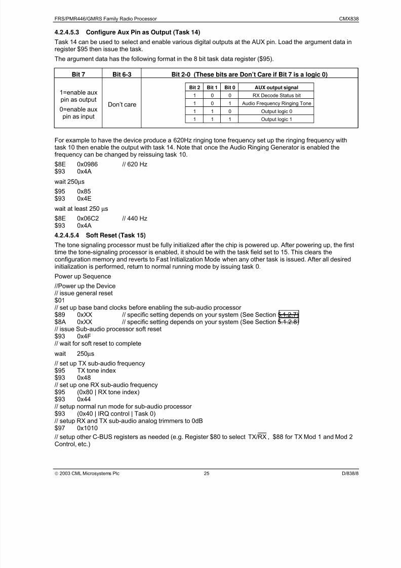
4.2.4.5.3 Configure Aux Pin as Output (Task 14)
Task 14 can be used to select and enable various digital outputs at the AUX pin. Load the argument data inregister $95 then issue the task.
The argument data has the following format in the 8 bit task data register ($95).
Bit 7 Bit 6-3 Bit 2-0 (These bits are Don’t Care if Bit 7 is a logic 0)
1=enable auxpin as output
0=enable auxpin as input
Don’t care
Bit 2 Bit 1 Bit 0 AUX output signal
1 0 0 RX Decode Status bit1 0 1 Audio Frequency Ringing Tone
1 1 0 Output logic 0
1 1 1 Output logic 1
For example to have the device produce a 620Hz ringing tone frequency set up the ringing frequency withtask 10 then enable the output with task 14. Note that once the Audio Ringing Generator is enabled thefrequency can be changed by reissuing task 10.
$8E 0x0986 // 620 Hz$93 0x4A
wait 250µs
$95 0x85$93 0x4E
wait at least 250 µs
$8E 0x06C2 // 440 Hz$93 0x4A
4.2.4.5.4 Soft Reset (Task 15)
The tone signaling processor must be fully initialized after the chip is powered up. After powering up, the firsttime the tone-signaling processor is enabled, it should be with the task field set to 15. This clears theconfiguration memory and reverts to Fast Initialization Mode when any other task is issued. After all desiredinitialization is performed, return to normal running mode by issuing task 0.
Power up Sequence
//Power up the Device// issue general reset$01// set up base band clocks before enabling the sub-audio processor $89 0xXX // specific setting depends on your system (See Section 5.1.2.7)$8A 0xXX // specific setting depends on your system (See Section 5.1.2.8)// issue Sub-audio processor soft reset$93 0x4F// wait for soft reset to complete
wait 250µs
// set up TX sub-audio frequency$95 TX tone index$93 0x48// set up one RX sub-audio frequency$95 (0x80 | RX tone index)$93 0x44// setup normal run mode for sub-audio processor $93 (0x40 | IRQ control | Task 0)// setup RX and TX sub-audio analog trimmers to 0dB$97 0x1010
// setup other C-BUS registers as needed (e.g. Register $80 to select RXTX/ , $88 for TX Mod 1 and Mod 2Control, etc.)
7/29/2019 Radio Gmrs Radio
http://slidepdf.com/reader/full/radio-gmrs-radio 26/72
FRS/PMR446/GMRS Family Radio Processor CMX838
2003 CML Microsystems Plc 26 D/838/8
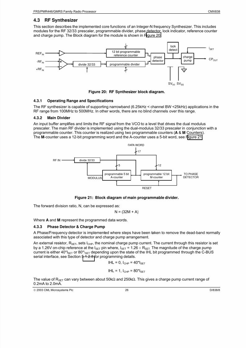
4.3 RF Synthesizer
This section describes the implemented core functions of an Integer-N frequency Synthesizer. This includesmodules for the RF 32/33 prescaler, programmable divider, phase detector, lock indicator, reference counter and charge pump. The Block diagram for the module is shown in Figure 20.
divide 32/33 programmable divider
12 bit programmablereference counter
phasedetector chargepump
lockdetect
-RFIN
+RFIN
REFIN
SVSS
ISET
CPOUT
S
SVDD
Figure 20: RF Synthesizer block diagram.
4.3.1 Operating Range and Specifications
The RF synthesizer is capable of supporting narrowband (6.25kHz < channel BW <25kHz) applications in theRF range from 100MHz to 500MHz. In other words, there are no blind channels over this range.
4.3.2 Main Divider
An input buffer amplifies and limits the RF signal from the VCO to a level that drives the dual modulusprescaler. The main RF divider is implemented using the dual-modulus 32/33 prescaler in conjunction with aprogrammable counter. This counter is realized using two programmable counters (A & M Counters).The M-counter uses a 12-bit programming word and the A-counter uses a 5-bit word, see Figure 21.
divide 32/33RF IN
programmable 5 bitA-counter
programmable 12 bitM-counter
TO PHASEDETECTOR
DATA WORD
5 12
17
RESET
MODULUS
Figure 21: Block diagram of main programmable divider.
The forward division ratio, N, can be expressed as:
N = (32M + A)
Where A and M represent the programmed data words.
4.3.3 Phase Detector & Charge Pump
A Phase/Frequency detector is implemented where steps have been taken to remove the dead-band normallyassociated with this type of detector and charge pump arrangement.
An external resistor, RSET, sets ICHP, the nominal charge pump current. The current through this resistor is setby a 1.26V on-chip reference at the ISET pin where, ISET = 1.26 ÷ RSET. The magnitude of the charge pumpcurrent is either 40*ISET or 80*ISET depending upon the state of the IHL bit programmed through the C-BUSserial interface, see Section 5.1.2.8 f or programming details.
IHL = 0, ICHP = 40*ISET
IHL = 1, ICHP = 80*ISET
The value of RSET can vary between about 50kΩ and 250kΩ. This gives a charge pump current range of 0.2mA to 2.0mA.
7/29/2019 Radio Gmrs Radio
http://slidepdf.com/reader/full/radio-gmrs-radio 27/72
FRS/PMR446/GMRS Family Radio Processor CMX838
2003 CML Microsystems Plc 27 D/838/8
4.3.4 Lock Detect Output
The Lock detect status is active high when the phase error corresponds to a time difference of less than about20ns, 40ns, 60ns, or 80ns at the phase detector comparison inputs. The comparison period is chosen usingthe Lock Delay bits of the Channel Select Register ($8B). The lock status is updated according to the lockdetect mode chosen using the Synthesizer General Control Register ($8A). Lock detect data is collected onceevery period of the reference signal.
4.3.5 Reference Circuits
The input from the external crystal oscillator is buffered and amplified to CMOS levels. This reference signal isthen divided in frequency by a 12-Bit programmable counter.
The Reference Divider is loaded from a ROM that yields one of four possible reference frequencies: 6.25kHz,12.5kHz, 20kHz, and 25kHz. Frequency selection is dependent on the RF service bits of the Synthesizer General Control Register ($8A) or two of the channel select bits when generic RF service is chosen ($8B).
4.4 Baseband Timing Generation
Internal baseband timing is developed from a configurable choice of two sources: a crystal clock signal(XTAL/CLOCK) or an externally applied synthesizer reference clock signal (REFIN). An on-chip crystaloscillator amplifier is provided to form a crystal oscillator via the addition of an external crystal.
Several frequency options are supported for both crystal and synthesizer clock source options.
Configuration details are described in Section 5.1.2.7.
7/29/2019 Radio Gmrs Radio
http://slidepdf.com/reader/full/radio-gmrs-radio 28/72
FRS/PMR446/GMRS Family Radio Processor CMX838
2003 CML Microsystems Plc 28 D/838/8
5 Software Programming
5.1 C-BUS Serial Interface
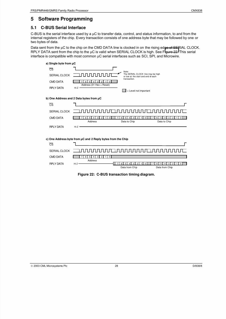
C-BUS is the serial interface used by a µC to transfer data, control, and status information, to and from theinternal registers of the chip. Every transaction consists of one address byte that may be followed by one or two bytes of data.
Data sent from the µC to the chip on the CMD DATA line is clocked in on the rising edge of SERIAL CLOCK.
RPLY DATA sent from the chip to the µC is valid when SERIAL CLOCK is high. See Figure 22. This serialinterface is compatible with most common µC serial interfaces such as SCI, SPI, and Microwire.
CS
a) Single byte from µC
SERIAL CLOCK
CMD DATAAddress (01 Hex = Reset)
= Level not important
Note:The SERIAL CLOCK line may be highor low at the start and end of eachtransaction.
Hi-ZRPLY DATA
7 6 5 4 3 2 1 0
7 6 5 4 3 2 1 0
c) One Address byte from µC and 2 Reply bytes from the Chip
CS
SERIAL CLOCK
Hi-ZAddress
Data from Chip Data from Chip
CMD DATA
RPLY DATA 7 6 5 4 3 2 1 0 7 6 5 4 3 2 1 0
b) One Address and 2 Data bytes from µC
CS
SERIAL CLOCK
CMD DATA
Address
Hi-Z
Data to Chip Data to Chip
RPLY DATA
7 6 5 4 3 2 1 0 7 6 5 4 3 2 1 0 7 6 5 4 3 2 1 0
Figure 22: C-BUS transaction timing diagram.
7/29/2019 Radio Gmrs Radio
http://slidepdf.com/reader/full/radio-gmrs-radio 29/72
FRS/PMR446/GMRS Family Radio Processor CMX838
2003 CML Microsystems Plc 29 D/838/8
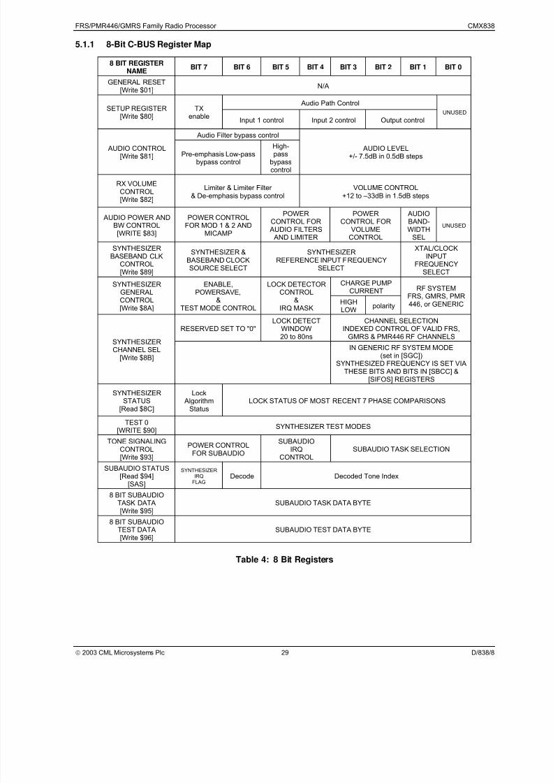
5.1.1 8-Bit C-BUS Register Map
8 BIT REGISTERNAME
BIT 7 BIT 6 BIT 5 BIT 4 BIT 3 BIT 2 BIT 1 BIT 0
GENERAL RESET[Write $01]
N/A
Audio Path ControlSETUP REGISTER
[Write $80]TX
enableInput 1 control Input 2 control Output control
UNUSED
Audio Filter bypass control
AUDIO CONTROL[Write $81] Pre-emphasis Low-pass
bypass control
High-pass
bypasscontrol
AUDIO LEVEL+/- 7.5dB in 0.5dB steps
RX VOLUMECONTROL[Write $82]
Limiter & Limiter Filter & De-emphasis bypass control
VOLUME CONTROL+12 to –33dB in 1.5dB steps
AUDIO POWER ANDBW CONTROL[WRITE $83]
POWER CONTROLFOR MOD 1 & 2 AND
MICAMP
POWERCONTROL FOR
AUDIO FILTERS AND LIMITER
POWERCONTROL FOR
VOLUMECONTROL
AUDIOBAND-WIDTH
SEL
UNUSED
SYNTHESIZERBASEBAND CLK
CONTROL[Write $89]
SYNTHESIZER &
BASEBAND CLOCKSOURCE SELECT
SYNTHESIZER
REFERENCE INPUT FREQUENCYSELECT
XTAL/CLOCKINPUT
FREQUENCYSELECT
CHARGE PUMPCURRENT
SYNTHESIZERGENERALCONTROL[Write $8A]
ENABLE,POWERSAVE,
&TEST MODE CONTROL
LOCK DETECTORCONTROL
&IRQ MASK
HIGHLOW
polarity
RF SYSTEMFRS, GMRS, PMR446, or GENERIC
RESERVED SET TO "0"LOCK DETECT
WINDOW20 to 80ns
CHANNEL SELECTIONINDEXED CONTROL OF VALID FRS,
GMRS & PMR446 RF CHANNELSSYNTHESIZERCHANNEL SEL
[Write $8B]
IN GENERIC RF SYSTEM MODE(set in [SGC])
SYNTHESIZED FREQUENCY IS SET VIATHESE BITS AND BITS IN [SBCC] &
[SIFOS] REGISTERS
SYNTHESIZERSTATUS[Read $8C]
Lock AlgorithmStatus
LOCK STATUS OF MOST RECENT 7 PHASE COMPARISONS
TEST 0[WRITE $90]
SYNTHESIZER TEST MODES
TONE SIGNALINGCONTROL[Write $93]
POWER CONTROLFOR SUBAUDIO
SUBAUDIOIRQ
CONTROLSUBAUDIO TASK SELECTION
SUBAUDIO STATUS[Read $94]
[SAS]
SYNTHESIZERIRQ
FLAGDecode Decoded Tone Index
8 BIT SUBAUDIOTASK DATA[Write $95]
SUBAUDIO TASK DATA BYTE
8 BIT SUBAUDIOTEST DATA[Write $96]
SUBAUDIO TEST DATA BYTE
Table 4: 8 Bit Registers
7/29/2019 Radio Gmrs Radio
http://slidepdf.com/reader/full/radio-gmrs-radio 30/72
FRS/PMR446/GMRS Family Radio Processor CMX838
2003 CML Microsystems Plc 30 D/838/8
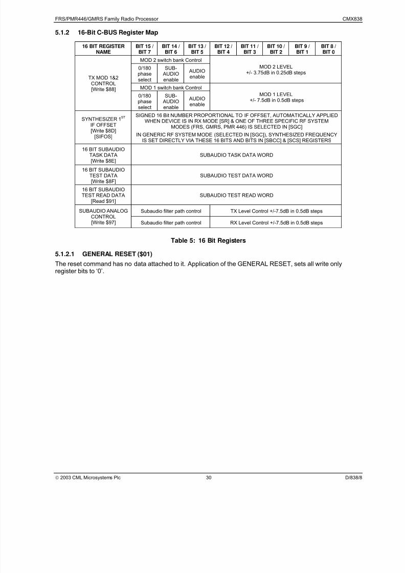
5.1.2 16-Bit C-BUS Register Map
16 BIT REGISTERNAME
BIT 15 /BIT 7
BIT 14 /BIT 6
BIT 13 /BIT 5
BIT 12 /BIT 4
BIT 11 /BIT 3
BIT 10 /BIT 2
BIT 9 /BIT 1
BIT 8 /BIT 0
MOD 2 switch bank Control
0/180phaseselect
SUB- AUDIOenable
AUDIOenable
MOD 2 LEVEL+/- 3.75dB in 0.25dB steps
MOD 1 switch bank Control
TX MOD 1&2CONTROL[Write $88]
0/180phaseselect
SUB- AUDIOenable
AUDIOenable
MOD 1 LEVEL+/- 7.5dB in 0.5dB steps
SYNTHESIZER 1ST IF OFFSET[Write $8D]
[SIFOS]
SIGNED 16 Bit NUMBER PROPORTIONAL TO IF OFFSET, AUTOMATICALLY APPLIEDWHEN DEVICE IS IN RX MODE [SR] & ONE OF THREE SPECIFIC RF SYSTEM
MODES (FRS, GMRS, PMR 446) IS SELECTED IN [SGC]
IN GENERIC RF SYSTEM MODE (SELECTED IN [SGC]), SYNTHESIZED FREQUENCYIS SET DIRECTLY VIA THESE 16 BITS AND BITS IN [SBCC] & [SCS] REGISTERS
16 BIT SUBAUDIOTASK DATA[Write $8E]
SUBAUDIO TASK DATA WORD
16 BIT SUBAUDIOTEST DATA[Write $8F]
SUBAUDIO TEST DATA WORD
16 BIT SUBAUDIOTEST READ DATA
[Read $91]SUBAUDIO TEST READ WORD
Subaudio filter path control TX Level Control +/-7.5dB in 0.5dB stepsSUBAUDIO ANALOGCONTROL[Write $97] Subaudio filter path control RX Level Control +/-7.5dB in 0.5dB steps
Table 5: 16 Bit Registers
5.1.2.1 GENERAL RESET ($01)
The reset command has no data attached to it. Application of the GENERAL RESET, sets all write onlyregister bits to ‘0’.
7/29/2019 Radio Gmrs Radio
http://slidepdf.com/reader/full/radio-gmrs-radio 31/72
FRS/PMR446/GMRS Family Radio Processor CMX838
2003 CML Microsystems Plc 31 D/838/8
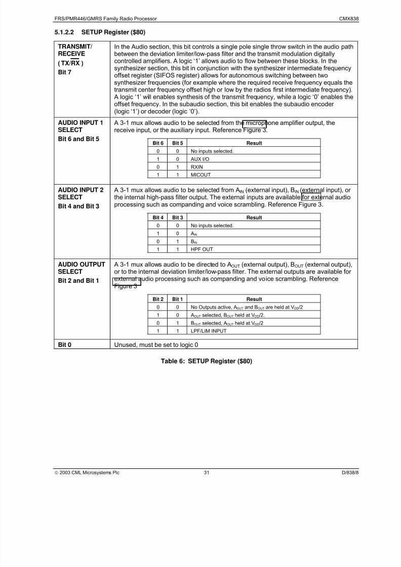
5.1.2.2 SETUP Register ($80)
TRANSMIT/RECEIVE
( RXTX/ )
Bit 7
In the Audio section, this bit controls a single pole single throw switch in the audio pathbetween the deviation limiter/low-pass filter and the transmit modulation digitallycontrolled amplifiers. A logic ‘1’ allows audio to flow between these blocks. In thesynthesizer section, this bit in conjunction with the synthesizer intermediate frequencyoffset register (SIFOS register) allows for autonomous switching between twosynthesizer frequencies (for example where the required receive frequency equals thetransmit center frequency offset high or low by the radios first intermediate frequency).
A logic ‘1’ will enables synthesis of the transmit frequency, while a logic ‘0’ enables theoffset frequency. In the subaudio section, this bit enables the subaudio encoder (logic ‘1’) or decoder (logic ‘0’).
AUDIO INPUT 1SELECT
Bit 6 and Bit 5
A 3-1 mux allows audio to be selected from the microphone amplifier output, thereceive input, or the auxiliary input. Reference Figure 3.
Bit 6 Bit 5 Result
0 0 No inputs selected.
1 0 AUX I/O
0 1 RXIN
1 1 MICOUT
AUDIO INPUT 2SELECT
Bit 4 and Bit 3
A 3-1 mux allows audio to be selected from AIN (external input), BIN (external input), or the internal high-pass filter output. The external inputs are available for external audioprocessing such as companding and voice scrambling. Reference Figure 3.
Bit 4 Bit 3 Result
0 0 No inputs selected.
1 0 AIN
0 1 BIN
1 1 HPF OUT
AUDIO OUTPUTSELECT
Bit 2 and Bit 1
A 3-1 mux allows audio to be directed to AOUT (external output), BOUT (external output),or to the internal deviation limiter/low-pass filter. The external outputs are available for external audio processing such as companding and voice scrambling. Reference
Figure 3
Bit 2 Bit 1 Result
0 0 No Outputs active, AOUT and BOUT are held at VDD/2
1 0 AOUT selected, BOUT held at VDD/2.
0 1 BOUT selected, AOUT held at VDD/2
1 1 LPF/LIM INPUT
Bit 0 Unused, must be set to logic 0
Table 6: SETUP Register ($80)

7/29/2019 Radio Gmrs Radio
http://slidepdf.com/reader/full/radio-gmrs-radio 32/72
FRS/PMR446/GMRS Family Radio Processor CMX838
2003 CML Microsystems Plc 32 D/838/8
5.1.2.3 AUDIO CONTROL Register ($81)
PRE-EMPHASIS/LPFCONTROL
(PRE LPF CTRL)
Bit 7 and Bit 6
The first stage of filtering following Input Mux 1 can be configured as a 2nd order low-pass filter, as a pre-emphasis network or bypassed. Reference Figure 3.
Bit 7 Bit 6 Result
0 0 Pre-emphasis
0 1 Low-pass filter
1 0 Mute, output is held to VDD/2
1 1 bypass
HIGHPASSFILTER BYPASS
Bit 5
When this bit is a Logic ‘1’ the high-pass audio filter is bypassed. Reference Figure 3.
Audio LevelBit 4,3,2,1,0
The five least significant bits in this register are used to set the gain/attenuation of theaudio level control as shown in the table below. This digitally controlled amplifier islocated in the audio path between the input low-pass filter/pre-emphasis network andthe 6
thorder high-pass filter. Its primary purpose is to trim the nominal audio level such
that the dynamic range is maximized.
4 3 2 1 0 AUDIO GAIN
0 0 0 0 0 Off 0 0 0 0 1 -7.5dB
0 0 0 1 0 -7.0dB
0 0 0 1 1 -6.5dB
0 0 1 0 0 -6.0dB
0 0 1 0 1 -5.5dB
0 0 1 1 0 -5.0dB
0 0 1 1 1 -4.5dB
0 1 0 0 0 -4.0dB
0 1 0 0 1 -3.5dB
0 1 0 1 0 -3.0dB
0 1 0 1 1 -2.5dB
0 1 1 0 0 -2.0dB0 1 1 0 1 -1.5dB
0 1 1 1 0 -1.0dB
0 1 1 1 1 -0.5dB
1 0 0 0 0 0.0dB
1 0 0 0 1 0.5dB
1 0 0 1 0 1.0dB
1 0 0 1 1 1.5dB
1 0 1 0 0 2.0dB
1 0 1 0 1 2.5dB
1 0 1 1 0 3.0dB
1 0 1 1 1 3.5dB
1 1 0 0 0 4.0dB1 1 0 0 1 4.5dB
1 1 0 1 0 5.0dB
1 1 0 1 1 5.5dB
1 1 1 0 0 6.0dB
1 1 1 0 1 6.5dB
1 1 1 1 0 7.0dB
1 1 1 1 1 7.5dB
Table 7: AUDIO CONTROL Register ($81)
7/29/2019 Radio Gmrs Radio
http://slidepdf.com/reader/full/radio-gmrs-radio 33/72
FRS/PMR446/GMRS Family Radio Processor CMX838
2003 CML Microsystems Plc 33 D/838/8
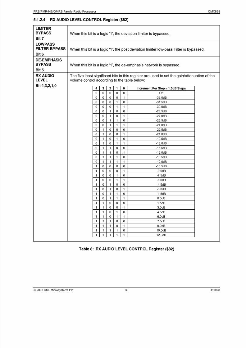
5.1.2.4 RX AUDIO LEVEL CONTROL Register ($82)
LIMITERBYPASS
Bit 7
When this bit is a logic ‘1’, the deviation limiter is bypassed.
LOWPASSFILTER BYPASS
Bit 6
When this bit is a logic ‘1’, the post deviation limiter low-pass Filter is bypassed.
DE-EMPHASISBYPASS
Bit 5
When this bit is a logic ‘1’, the de-emphasis network is bypassed.
RX AUDIOLEVEL
Bit 4,3,2,1,0
The five least significant bits in this register are used to set the gain/attenuation of thevolume control according to the table below:
4 3 2 1 0 Increment Per Step = 1.5dB Steps
0 0 0 0 0 Off
0 0 0 0 1 -33.0dB
0 0 0 1 0 -31.5dB
0 0 0 1 1 -30.0dB
0 0 1 0 0 -28.5dB
0 0 1 0 1 -27.0dB0 0 1 1 0 -25.5dB
0 0 1 1 1 -24.0dB
0 1 0 0 0 -22.5dB
0 1 0 0 1 -21.0dB
0 1 0 1 0 -19.5dB
0 1 0 1 1 -18.0dB
0 1 1 0 0 -16.5dB
0 1 1 0 1 -15.0dB
0 1 1 1 0 -13.5dB
0 1 1 1 1 -12.0dB
1 0 0 0 0 -10.5dB
1 0 0 0 1 -9.0dB
1 0 0 1 0 -7.5dB1 0 0 1 1 -6.0dB
1 0 1 0 0 -4.5dB
1 0 1 0 1 -3.0dB
1 0 1 1 0 -1.5dB
1 0 1 1 1 0.0dB
1 1 0 0 0 1.5dB
1 1 0 0 1 3.0dB
1 1 0 1 0 4.5dB
1 1 0 1 1 6.0dB
1 1 1 0 0 7.5dB
1 1 1 0 1 9.0dB
1 1 1 1 0 10.5dB
1 1 1 1 1 12.0dB
Table 8: RX AUDIO LEVEL CONTROL Register ($82)

7/29/2019 Radio Gmrs Radio
http://slidepdf.com/reader/full/radio-gmrs-radio 34/72
FRS/PMR446/GMRS Family Radio Processor CMX838
2003 CML Microsystems Plc 34 D/838/8
5.1.2.5 AUDIO POWER AND BANDWIDTH CONTROL Register ($83)
TX MOD andMIC AMPLIFIERPOWERCONTROLBit 7 and Bit 6
These bits are dedicated to power control for the modulation digitally controlledamplifiers and the microphone amplifier
Bit 7 Bit 6 Power level setting
0 0 Power down (off)
0 1 Normal Operation
AUDIO FILTERPOWERCONTROL
Bit 5 and Bit 4
These bits are dedicated to power control for the audio filters, the deviation limiter, andthe audio level digitally controlled amplifier
Bit 5 Bit 4 Power level setting
0 0 Power down (off)
0 1 Normal Operation
RX AUDIO OUTPOWERCONTROL
Bit 3 and Bit 2
These bits are dedicated to power control for the de-emphasis network and theRX Audio Out digitally controlled amplifier.
Bit 3 Bit 2 Power level setting
0 0 Power down (off)
0 1 Normal Operation
AUDIOBANDWIDTHCONTROL
Bit 1
A logic ‘1’ on this bit reduces the –3dB bandwidth of the post deviation limiter low-passfilter from 3.5kHz to 3.0kHz. The narrow band setting is intended for radio systems withRF channel bandwidths ≤ 12.5kHz.
Bit 0 Unused, must be set to Logic ‘0’
Table 9: AUDIO POWER AND BANDWIDTH CONTROL Register ($83)
7/29/2019 Radio Gmrs Radio
http://slidepdf.com/reader/full/radio-gmrs-radio 35/72
FRS/PMR446/GMRS Family Radio Processor CMX838
2003 CML Microsystems Plc 35 D/838/8
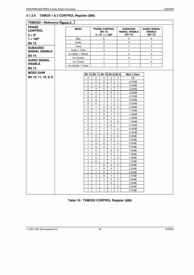
5.1.2.6 TXMOD 1 & 2 CONTROL Register ($88)
TXMOD2 – Reference Figure 3
PHASECONTROL
0 = 0°°°° 1 = 180°°°°
Bit 15
SUBAUDIOSIGNAL ENABLE
Bit 14
AUDIO SIGNALENABLE
Bit 13
MOD2 PHASE CONTROL(Bit 15)
0 = 0°°°°, 1 = 180°°°°
SUBAUDIOSIGNAL ENABLE
(Bit 14)
AUDIO SIGNALENABLE(Bit 13)
Bias 0 0 0
Audio 0 0 1
Tone 0 1 0 Audio + Tone 0 1 1
Inv (Bias + Offset) 1 0 0
Inv (Audio) 1 0 1
Inv (Tone) 1 1 0
Inv (Audio + Tone) 1 1 1
MOD2 GAIN
Bit 12, 11, 10, 9, 8Bit 12 Bit 11 Bit 10 Bit 9 Bit 8 Mod. 2 Gain
0 0 0 0 0 Off
0 0 0 0 1 -3.75dB
0 0 0 1 0 -3.50dB
0 0 0 1 1 -3.25dB
0 0 1 0 0 -3.00dB0 0 1 0 1 -2.75dB
0 0 1 1 0 -2.50dB
0 0 1 1 1 -2.25dB
0 1 0 0 0 -2.00dB
0 1 0 0 1 -1.75dB
0 1 0 1 0 -1.50dB
0 1 0 1 1 -1.25dB
0 1 1 0 0 -1.00dB
0 1 1 0 1 -0.75dB
0 1 1 1 0 -0.50dB
0 1 1 1 1 -0.25dB
1 0 0 0 0 0.00dB
1 0 0 0 1 0.25dB
1 0 0 1 0 0.50dB
1 0 0 1 1 0.75dB
1 0 1 0 0 1.00dB
1 0 1 0 1 1.25dB
1 0 1 1 0 1.50dB
1 0 1 1 1 1.75dB
1 1 0 0 0 2.00dB
1 1 0 0 1 2.25dB
1 1 0 1 0 2.50dB
1 1 0 1 1 2.75dB
1 1 1 0 0 3.00dB
1 1 1 0 1 3.25dB
1 1 1 1 0 3.50dB
1 1 1 1 1 3.75dB
Table 10: TXMOD2 CONTROL Register ($88)
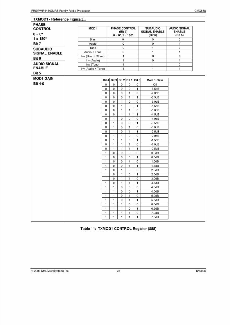
7/29/2019 Radio Gmrs Radio
http://slidepdf.com/reader/full/radio-gmrs-radio 36/72
FRS/PMR446/GMRS Family Radio Processor CMX838
2003 CML Microsystems Plc 36 D/838/8
TXMOD1 - Reference Figure 3
PHASECONTROL
0 = 0°°°° 1 = 180°°°°
Bit 7
SUBAUDIO
SIGNAL ENABLEBit 6
AUDIO SIGNALENABLE
Bit 5
MOD1 PHASE CONTROL(Bit 7)
0 = 0°°°°, 1 = 180°°°°
SUBAUDIOSIGNAL ENABLE
(Bit 6)
AUDIO SIGNALENABLE
(Bit 5)
Bias 0 0 0
Audio 0 0 1
Tone 0 1 0
Audio + Tone 0 1 1
Inv (Bias + Offset) 1 0 0
Inv (Audio) 1 0 1
Inv (Tone) 1 1 0
Inv (Audio + Tone) 1 1 1
MOD1 GAIN
Bit 4-0Bit 4 Bit 3 Bit 2 Bit 1 Bit 0 Mod. 1 Gain
0 0 0 0 0 Off
0 0 0 0 1 -7.5dB
0 0 0 1 0 -7.0dB
0 0 0 1 1 -6.5dB
0 0 1 0 0 -6.0dB
0 0 1 0 1 -5.5dB
0 0 1 1 0 -5.0dB
0 0 1 1 1 -4.5dB
0 1 0 0 0 -4.0dB
0 1 0 0 1 -3.5dB
0 1 0 1 0 -3.0dB
0 1 0 1 1 -2.5dB
0 1 1 0 0 -2.0dB
0 1 1 0 1 -1.5dB
0 1 1 1 0 -1.0dB
0 1 1 1 1 -0.5dB
1 0 0 0 0 0.0dB
1 0 0 0 1 0.5dB
1 0 0 1 0 1.0dB
1 0 0 1 1 1.5dB
1 0 1 0 0 2.0dB
1 0 1 0 1 2.5dB
1 0 1 1 0 3.0dB
1 0 1 1 1 3.5dB
1 1 0 0 0 4.0dB
1 1 0 0 1 4.5dB
1 1 0 1 0 5.0dB
1 1 0 1 1 5.5dB
1 1 1 0 0 6.0dB
1 1 1 0 1 6.5dB
1 1 1 1 0 7.0dB
1 1 1 1 1 7.5dB
Table 11: TXMOD1 CONTROL Register ($88)
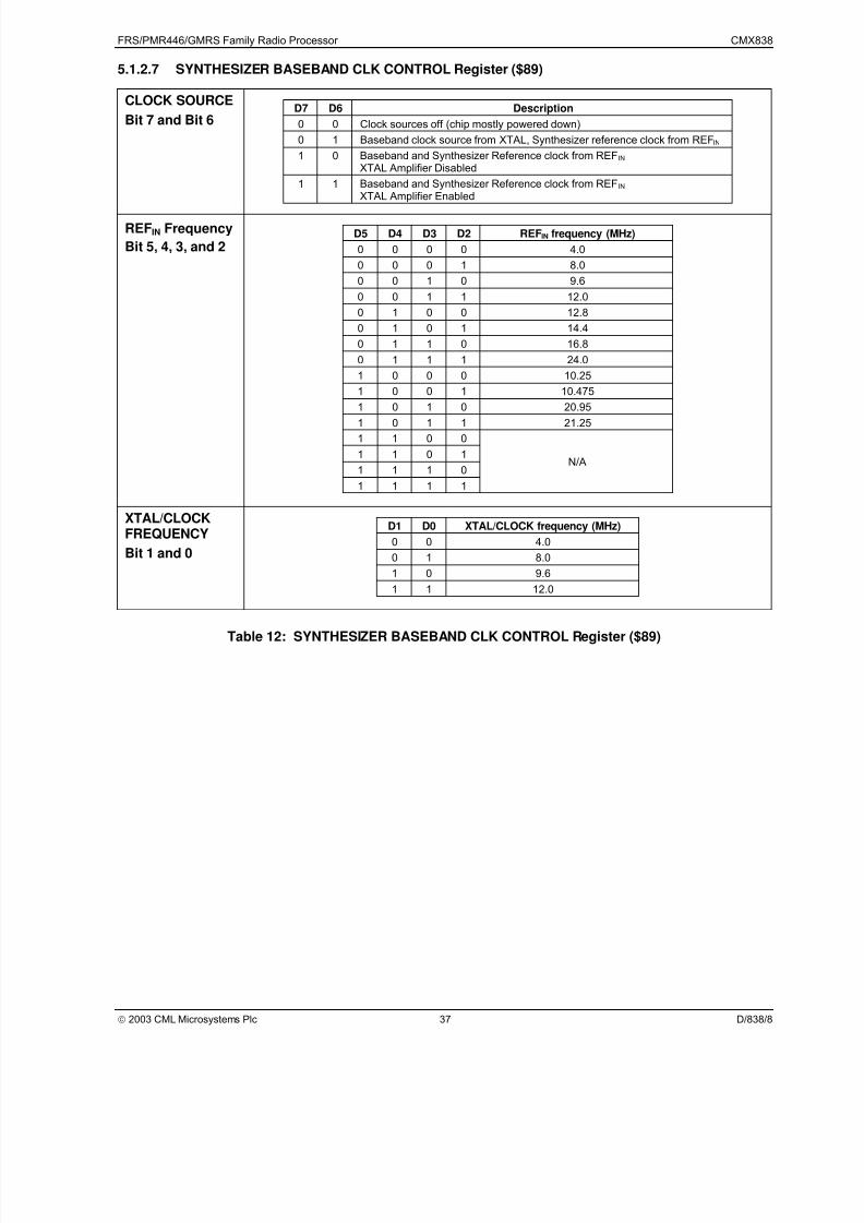
7/29/2019 Radio Gmrs Radio
http://slidepdf.com/reader/full/radio-gmrs-radio 37/72
FRS/PMR446/GMRS Family Radio Processor CMX838
2003 CML Microsystems Plc 37 D/838/8
5.1.2.7 SYNTHESIZER BASEBAND CLK CONTROL Register ($89)
CLOCK SOURCE
Bit 7 and Bit 6D7 D6 Description
0 0 Clock sources off (chip mostly powered down)
0 1 Baseband clock source from XTAL, Synthesizer reference clock from REFIN
1 0 Baseband and Synthesizer Reference clock from REFIN XTAL Amplifier Disabled
1 1 Baseband and Synthesizer Reference clock from REFIN XTAL Amplifier Enabled
REFIN Frequency
Bit 5, 4, 3, and 2D5 D4 D3 D2 REFIN frequency (MHz)
0 0 0 0 4.0
0 0 0 1 8.0
0 0 1 0 9.6
0 0 1 1 12.0
0 1 0 0 12.8
0 1 0 1 14.4
0 1 1 0 16.8
0 1 1 1 24.0
1 0 0 0 10.25
1 0 0 1 10.475
1 0 1 0 20.951 0 1 1 21.25
1 1 0 0
1 1 0 1
1 1 1 0
1 1 1 1
N/A
XTAL/CLOCKFREQUENCY
Bit 1 and 0
D1 D0 XTAL/CLOCK frequency (MHz)
0 0 4.0
0 1 8.0
1 0 9.6
1 1 12.0
Table 12: SYNTHESIZER BASEBAND CLK CONTROL Register ($89)

7/29/2019 Radio Gmrs Radio
http://slidepdf.com/reader/full/radio-gmrs-radio 38/72
FRS/PMR446/GMRS Family Radio Processor CMX838
2003 CML Microsystems Plc 38 D/838/8
5.1.2.8 SYNTHESIZER GENERAL CONTROL Register ($8A)
SYNTHESIZERPOWERCONTROL
Bit 7 and Bit 6
D7 D6 Description
0 0 Synthesizer is powered down
0 1 Synthesizer is enabled.
1 0 Synthesizer Reference Clock Buffer is powered -the remainder of the Synthesizer is powered down.
1 1 Reserved for Test Mode.
LOCK CONTROL
Bit 5 and Bit 4D5 D4 Description
0 0 Lock Detect IRQ is masked
0 1 Lock Detect IRQ is enabled (status updated every phasecomparison when the last two comparisons disagree)
1 0 Lock Detect IRQ is enabled (IRQ updated instantly for loss of lock, IRQ updated after 8 consecutive in-lock phase compares toindicate lock)
1 1 Lock Detect IRQ is enabled (IRQ updated after 4 out of lockcomparisons during the last 8, IRQ updated after 16 consecutivein-lock phase compares to indicate lock).
IHL
Bit 3
Reference Section 4.3.3 Phase Detector and Charge Pump
D3 Description0 ICHP = 40 ISET
1 ICHP = 80 ISET
POLARITY OFCHARGE PUMPOUTPUT
Bit 2
D2 Description
0 Negative VCO V/F slope
1 Positive VCO V/F slope)
RF SERVICE
Bit 1 and Bit 0D1 D0 Description
0 0 Select FRS channels (SYNTHREF = 12.5kHz )
0 1 Select PMR 446 channels (SYNTHREF = 6.25kHz)
1 0
Select GMSR channels (SYNTHREF = 12.5kHz )
(this does not include the upper frequency band of GMRS which isreserved for duplex operation in a GMRS system)
1 1 Generic System (RF and Reference Dividers are Directly programmed)
Table 13: SYNTHESIZER GENERAL CONTROL Register ($8A)
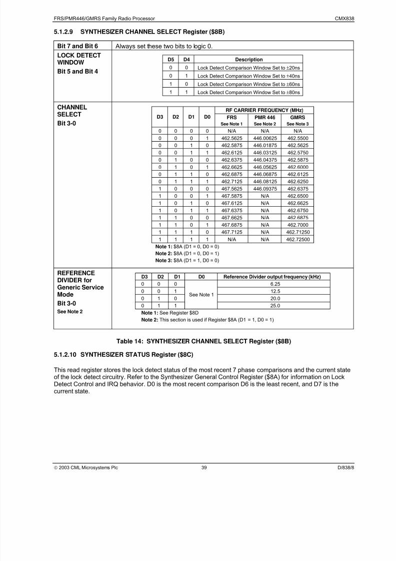
7/29/2019 Radio Gmrs Radio
http://slidepdf.com/reader/full/radio-gmrs-radio 39/72
FRS/PMR446/GMRS Family Radio Processor CMX838
2003 CML Microsystems Plc 39 D/838/8
5.1.2.9 SYNTHESIZER CHANNEL SELECT Register ($8B)
Bit 7 and Bit 6 Always set these two bits to logic 0.
LOCK DETECTWINDOW
Bit 5 and Bit 4
D5 D4 Description
0 0 Lock Detect Comparison Window Set to ±20ns
0 1 Lock Detect Comparison Window Set to ±40ns
1 0 Lock Detect Comparison Window Set to ±60ns
1 1 Lock Detect Comparison Window Set to ±80ns
CHANNELSELECT
Bit 3-0
RF CARRIER FREQUENCY (MHz)
D3 D2 D1 D0 FRS
See Note 1
PMR 446
See Note 2
GMRS
See Note 3
0 0 0 0 N/A N/A N/A
0 0 0 1 462.5625 446.00625 462.5500
0 0 1 0 462.5875 446.01875 462.5625
0 0 1 1 462.6125 446.03125 462.5750
0 1 0 0 462.6375 446.04375 462.5875
0 1 0 1 462.6625 446.05625 462.6000
0 1 1 0 462.6875 446.06875 462.6125
0 1 1 1 462.7125 446.08125 462.6250
1 0 0 0 467.5625 446.09375 462.63751 0 0 1 467.5875 N/A 462.6500
1 0 1 0 467.6125 N/A 462.6625
1 0 1 1 467.6375 N/A 462.6750
1 1 0 0 467.6625 N/A 462.6875
1 1 0 1 467.6875 N/A 462.7000
1 1 1 0 467.7125 N/A 462.71250
1 1 1 1 N/A N/A 462.72500
Note 1: $8A (D1 = 0, D0 = 0)
Note 2: $8A (D1 = 0, D0 = 1)
Note 3: $8A (D1 = 1, D0 = 0)
REFERENCE
DIVIDER forGeneric ServiceMode
Bit 3-0
See Note 2
D3 D2 D1 D0 Reference Divider output frequency (kHz)
0 0 0 6.250 0 1 12.5
0 1 0 20.0
0 1 1
See Note 1
25.0
Note 1: See Register $8D
Note 2: This section is used if Register $8A (D1 = 1, D0 = 1)
Table 14: SYNTHESIZER CHANNEL SELECT Register ($8B)
5.1.2.10 SYNTHESIZER STATUS Register ($8C)
This read register stores the lock detect status of the most recent 7 phase comparisons and the current state
of the lock detect circuitry. Refer to the Synthesizer General Control Register ($8A) for information on LockDetect Control and IRQ behavior. D0 is the most recent comparison D6 is the least recent, and D7 is thecurrent state.
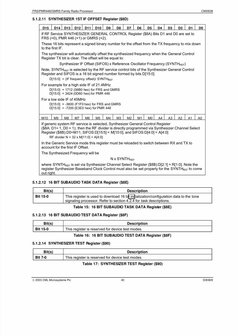
7/29/2019 Radio Gmrs Radio
http://slidepdf.com/reader/full/radio-gmrs-radio 40/72
FRS/PMR446/GMRS Family Radio Processor CMX838
2003 CML Microsystems Plc 40 D/838/8
5.1.2.11 SYNTHESIZER 1ST IF OFFSET Register ($8D)
D15 D14 D13 D12 D11 D10 D9 D8 D7 D6 D5 D4 D3 D2 D1 D0
If RF Service SYNTHESIZER GENERAL CONTROL Register ($8A) Bits D1 and D0 are set toFRS (=0), PMR 446 (=1) or GMRS (=2).
These 16 bits represent a signed binary number for the offset from the TX frequency to mix downto the first IF.
The synthesizer will automatically offset the synthesized frequency when the General ControlRegister TX bit is clear. The offset will be equal to:
Synthesizer IF Offset (SIFOS) x Reference Oscillator Frequency (SYNTHREF)
Note, SYNTHREF is selected by the RF service control bits of the Synthesizer General ControlRegister and SIFOS is a 16 bit signed number formed by bits D[15:0]
D[15:0] = (IF frequency offset)/ SYNTHREF
For example for a high side IF of 21.4MHz
D[15:0] = 1712 (06B0 hex) for FRS and GMRSD[15:0] = 3424 (0D60 hex) for PMR 446
For a low side IF of 45MHzD[15:0] = -3600 (F1F0 hex) for FRS and GMRSD[15:0] = -7200 (E3E0 hex) for PMR 446
M10 M9 M8 M7 M6 M5 M4 M3 M2 M1 M0 A4 A3 A2 A1 A0
If generic system RF service is selected, Synthesizer General Control Register ($8A: D1= 1, D0 = 1); then the RF divider is directly programmed via Synthesizer Channel SelectRegister ($8B):D0=M11, SIFOS:D[15:5] = M[10:0], and SIFOS:D[4:0] = A[4:0]
RF divider N = 32 x M[11:0] + A[4:0]
In the Generic Service mode this register must be reloaded to switch between RX and TX toaccount for the first IF Offset.
The Synthesized Frequency will be
N x SYNTHREF
where SYNTHREF is set via Synthesizer Channel Select Register ($8B):D[2:1] = R[1:0]. Note the
register Synthesizer Baseband Clock Control must also be set properly for the SYNTHREF to comeout right.
5.1.2.12 16 BIT SUBAUDIO TASK DATA Register ($8E)
Bit(s) Description
Bit 15-0 This register is used to download 16 bit initialization/configuration data to the tonesignaling processor. Refer to section 4.2.4 for task descriptions.
Table 15: 16 BIT SUBAUDIO TASK DATA Register ($8E)
5.1.2.13 16 BIT SUBAUDIO TEST DATA Register ($8F)
Bit(s) Description
Bit 15-0 This register is reserved for device test modes.
Table 16: 16 BIT SUBAUDIO TEST DATA Register ($8F)
5.1.2.14 SYNTHESIZER TEST Register ($90)
Bit(s) Description
Bit 7-0 This register is reserved for device test modes.
Table 17: SYNTHESIZER TEST Register ($90)
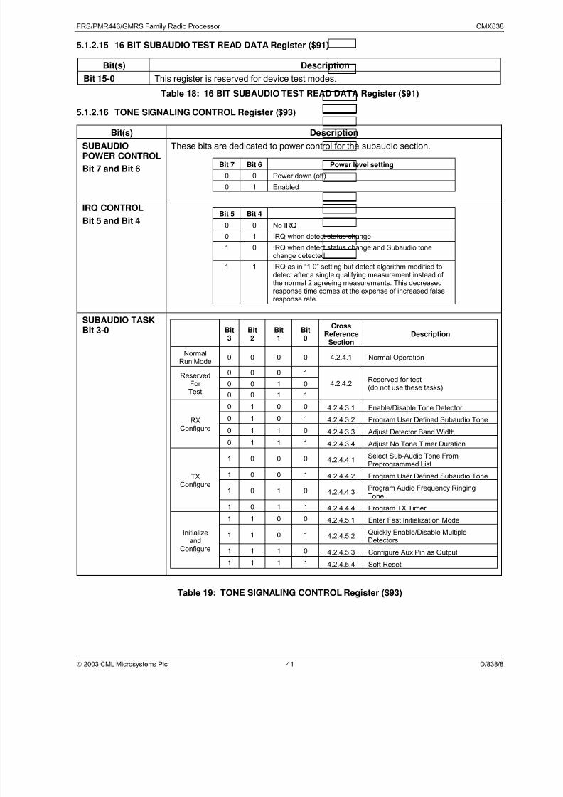
7/29/2019 Radio Gmrs Radio
http://slidepdf.com/reader/full/radio-gmrs-radio 41/72
FRS/PMR446/GMRS Family Radio Processor CMX838
2003 CML Microsystems Plc 41 D/838/8
5.1.2.15 16 BIT SUBAUDIO TEST READ DATA Register ($91)
Bit(s) Description
Bit 15-0 This register is reserved for device test modes.
Table 18: 16 BIT SUBAUDIO TEST READ DATA Register ($91)
5.1.2.16 TONE SIGNALING CONTROL Register ($93)
Bit(s) Description SUBAUDIOPOWER CONTROL
Bit 7 and Bit 6
These bits are dedicated to power control for the subaudio section.
Bit 7 Bit 6 Power level setting
0 0 Power down (off )
0 1 Enabled
IRQ CONTROL
Bit 5 and Bit 4Bit 5 Bit 4
0 0 No IRQ
0 1 IRQ when detect status change
1 0 IRQ when detect status change and Subaudio tonechange detected
1 1 IRQ as in “1 0” setting but detect algorithm modified todetect after a single qualifying measurement instead of the normal 2 agreeing measurements. This decreasedresponse time comes at the expense of increased falseresponse rate.
SUBAUDIO TASKBit 3-0 Bit
3Bit2
Bit1
Bit0
CrossReference
SectionDescription
NormalRun Mode
0 0 0 0 4.2.4.1 Normal Operation
0 0 0 1
0 0 1 0Reserved
For Test 0 0 1 1
4.2.4.2Reserved for test(do not use these tasks)
0 1 0 0 4.2.4.3.1 Enable/Disable Tone Detector
0 1 0 1 4.2.4.3.2 Program User Defined Subaudio Tone
0 1 1 0 4.2.4.3.3 Adjust Detector Band Width
RXConfigure
0 1 1 1 4.2.4.3.4 Adjust No Tone Timer Duration
1 0 0 0 4.2.4.4.1Select Sub-Audio Tone FromPreprogrammed List
1 0 0 1 4.2.4.4.2 Program User Defined Subaudio Tone
1 0 1 0 4.2.4.4.3Program Audio Frequency RingingTone
TXConfigure
1 0 1 1 4.2.4.4.4 Program TX Timer
1 1 0 0 4.2.4.5.1 Enter Fast Initialization Mode
1 1 0 1 4.2.4.5.2Quickly Enable/Disable MultipleDetectors
1 1 1 0 4.2.4.5.3 Configure Aux Pin as Output
InitializeandConfigure
1 1 1 1 4.2.4.5.4 Soft Reset
Table 19: TONE SIGNALING CONTROL Register ($93)

7/29/2019 Radio Gmrs Radio
http://slidepdf.com/reader/full/radio-gmrs-radio 42/72
FRS/PMR446/GMRS Family Radio Processor CMX838
2003 CML Microsystems Plc 42 D/838/8
5.1.2.17 SUBAUDIO STATUS Register ($94)
Bit(s) Description
SYNTH_IRQ
Bit 7
This bit indicates whether the synthesizer lock detector issued an IRQ since the lastread of the synthesizer status register. Once the lock detector issues an IRQ this bitbecomes a logic ‘1’ and the chip IRQ pin is pulled low. SYNTH_IRQ bit remains a logic‘1’ until the synthesizer status register is read. However, the chip’s IRQ is cleared assoon as this subaudio status register is read. In other words, when servicing an IRQ,
read the subaudio status register and check this bit to determine if the synthesizer needs servicing.
DECODERSTATUS
Bit 6
In RX mode, the decode status bit is a logic one when an enabled decoder senses thatthe input signal matches its center frequency and is of sufficient quality to decode
In TX mode, bits 6-0 are normally zero, but take the decimal value 127 to indicate whenthe TX timer has expired.
Reading the status register resets bits 6-0 to zero as well as clearing the IRQ in TXmode to allow recurring indication of TX timer expiration. In RX mode, only the IRQ iscleared on reading this status register, while the decode status and tone index aremaintained and continuously reported here.
TONE INDEXNUMBER
Bit 5-0
Refer to Table 2 for supported Tone List and their index numbers.
Index numbers 1-51 indicate a matching decoder (enabled decoder index may be
reported before the full decode qualification of 2 matching measurements).In TX mode, bits 6-0 are normally zero, but take the decimal value 127 to indicate whenthe TX timer has expired.
If the input signal does not contain a subaudio signal that matches an enableddecoder’s center frequency then the decoder status bit is a logic zero – in this case thedecoder index number is reported as:
• 62 if there is a significant subaudio frequency present outside the bandwidth of any enabled decoder.
• 63 if the no tone timer has expired indicating (i.e. there is no significantsubaudio frequency present currently)
• 0 if no subaudio signal has been seen since the subaudio processor wasenabled or most recently placed in RX mode.
• Any enabled index, if the last frequency measurement indicates that enabledtone may be present but has not yet been fully qualified.
Table 20: SUBAUDIO STATUS Register ($94)
5.1.2.18 8 BIT SUBAUDIO TASK DATA Register ($95)
Bit(s) Description
Bit 7-0 This register is used to download 8 bit initialization/configuration data to the subaudioprocessor. Refer to section 4.2.4 for task descriptions.
Table 21: 8 BIT SUBAUDIO TASK DATA Register ($95)

7/29/2019 Radio Gmrs Radio
http://slidepdf.com/reader/full/radio-gmrs-radio 43/72
FRS/PMR446/GMRS Family Radio Processor CMX838
2003 CML Microsystems Plc 43 D/838/8
5.1.2.19 SUBAUDIO ANALOG CONTROL Register ($97)
Bit(s) Description
SUBAUDIOFILTER INPUTSELECT
Bit 15
Bit 15 in conjunction with RXTX/ bit (bit 7) of the SETUP Register ($80) controls theinput signal source of the subaudio filter according to the following table:
Bit 15 RXTX/ Input Source
0 0 RXIN pin
0 1 Encoder D/A1 0 Encoder D/A
1 1 RXIN pin
Bit 15 in conjunction with RXTX/ form the DECODE control signal of the subaudioanalog block according to the above table. In normal operation, this bit should be alogic ‘0’.
SUBAUDIOLOW PASSFILTER 1 GAIN
Bit 14
Bit 14 in conjunction with RXTX/ bit (bit 7) of the SETUP Register ($80) controls thegain of the subaudio low pass filter, which is the second subaudio filter stage. The lowpass filter gain is set according to the following table:
Bit 14 RXTX/ Gain (dB)
0 0 +20
0 1 0
1 0 0
1 1 +20
The default gain setting is 0dB for TX mode and +20dB for RX mode. Setting gain to+20dB in TX mode will overdrive the low pass filter resulting in distorted signals. Thisbit should be a logic ‘0’ for normal operation.
SUBAUDIOHIGH PASSFILTER/ LOWPASS FILTERSELECT
Bit 13
Bit 13 in conjunction with RXTX/ bit (bit 7) of the SETUP Register ($80) controls thesubaudio filter characteristic of the 2nd filter stage according to the following table:
Bit 13 RXTX/ Characteristic
0 0 65Hz High Pass DC Blocking Filter
0 1 2kHz Low Pass Smoothing Filter
1 0 2kHz Low Pass Smoothing Filter
1 1 65Hz High Pass DC Blocking Filter
The nominal gain of this 2nd subaudio filter stage is 0dB for HPF mode and –18dB for LPF mode. See Bit 7 description for setting Low Pass Filter 2 gain to 0dB. This bitshould be a logic ‘0’ for normal operation.

7/29/2019 Radio Gmrs Radio
http://slidepdf.com/reader/full/radio-gmrs-radio 44/72
FRS/PMR446/GMRS Family Radio Processor CMX838
2003 CML Microsystems Plc 44 D/838/8
Bit(s) Description
TX SUBAUDIOLEVEL
Bit 12-8
Bit 12 Bit 11 Bit 10 Bit 9 Bit 8 Subaudio Gain
0 0 0 0 0 Off
0 0 0 0 1 -7.5dB
0 0 0 1 0 -7.0dB
0 0 0 1 1 -6.5dB
0 0 1 0 0 -6.0dB
0 0 1 0 1 -5.5dB
0 0 1 1 0 -5.0dB
0 0 1 1 1 -4.5dB
0 1 0 0 0 -4.0dB
0 1 0 0 1 -3.5dB
0 1 0 1 0 -3.0dB
0 1 0 1 1 -2.5dB
0 1 1 0 0 -2.0dB
0 1 1 0 1 -1.5dB
0 1 1 1 0 -1.0dB
0 1 1 1 1 -0.5dB
1 0 0 0 0 0.0dB
1 0 0 0 1 0.5dB
1 0 0 1 0 1.0dB
1 0 0 1 1 1.5dB
1 0 1 0 0 2.0dB
1 0 1 0 1 2.5dB
1 0 1 1 0 3.0dB
1 0 1 1 1 3.5dB
1 1 0 0 0 4.0dB
1 1 0 0 1 4.5dB
1 1 0 1 0 5.0dB
1 1 0 1 1 5.5dB
1 1 1 0 0 6.0dB
1 1 1 0 1 6.5dB
1 1 1 1 0 7.0dB
1 1 1 1 1 7.5dB
SUBAUDIOLOW PASSFILTER 2 GAIN
Bit 7
Setting to a logic ‘1’ forces 2nd subaudio filter stage to have 0dB gain in LPF mode,resulting in a Gain boost of 18dB over the normal setting. Used in conjunction with bit13 this can allow an RX signal path with pass band response down to DC with anominal overall pass band gain of 22dB. In normal operation, this bit should be a logic‘0’.
SUBAUDIOFILTEROUTPUTENABLE
Bit 6
This bit can be used to expose the Subaudio filter output through the MOD block in RXmode. Normally the Subaudio filter output is only connected to the MOD block in TXmode. Setting this bit to a logic ‘1’ connects the filter output to the MOD block in bothTX and RX modes. In normal operation, this bit should be a logic ‘0’.
DC
RESTORATIONBit 5
Set this bit to a logic ‘1’ to enable external DC restore mode. In external DC restore
mode, an external capacitor to ground at the AUX I/O pin is required to compensate for internal filter offsets. In normal operation, this bit should be a logic ‘0’.
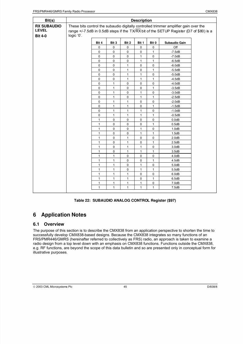
7/29/2019 Radio Gmrs Radio
http://slidepdf.com/reader/full/radio-gmrs-radio 45/72
FRS/PMR446/GMRS Family Radio Processor CMX838
2003 CML Microsystems Plc 45 D/838/8
Bit(s) Description
RX SUBAUDIOLEVEL
Bit 4-0
These bits control the subaudio digitally controlled trimmer amplifier gain over the
range +/-7.5dB in 0.5dB steps if the RXTX/ bit of the SETUP Register (D7 of $80) is alogic ‘0’.
Bit 4 Bit 3 Bit 2 Bit 1 Bit 0 Subaudio Gain
0 0 0 0 0 Off
0 0 0 0 1 -7.5dB
0 0 0 1 0 -7.0dB0 0 0 1 1 -6.5dB
0 0 1 0 0 -6.0dB
0 0 1 0 1 -5.5dB
0 0 1 1 0 -5.0dB
0 0 1 1 1 -4.5dB
0 1 0 0 0 -4.0dB
0 1 0 0 1 -3.5dB
0 1 0 1 0 -3.0dB
0 1 0 1 1 -2.5dB
0 1 1 0 0 -2.0dB
0 1 1 0 1 -1.5dB
0 1 1 1 0 -1.0dB
0 1 1 1 1 -0.5dB1 0 0 0 0 0.0dB
1 0 0 0 1 0.5dB
1 0 0 1 0 1.0dB
1 0 0 1 1 1.5dB
1 0 1 0 0 2.0dB
1 0 1 0 1 2.5dB
1 0 1 1 0 3.0dB
1 0 1 1 1 3.5dB
1 1 0 0 0 4.0dB
1 1 0 0 1 4.5dB
1 1 0 1 0 5.0dB
1 1 0 1 1 5.5dB
1 1 1 0 0 6.0dB1 1 1 0 1 6.5dB
1 1 1 1 0 7.0dB
1 1 1 1 1 7.5dB
Table 22: SUBAUDIO ANALOG CONTROL Register ($97)
6 Application Notes
6.1 Overview
The purpose of this section is to describe the CMX838 from an application perspective to shorten the time tosuccessfully develop CMX838-based designs. Because the CMX838 integrates so many functions of anFRS/PMR446/GMRS (hereinafter referred to collectively as FRS) radio, an approach is taken to examine aradio design from a top level down with an emphasis on CMX838 functions. Functions outside the CMX838,e.g. RF functions, are beyond the scope of this data bulletin and so are presented only in conceptual form for illustrative purposes.
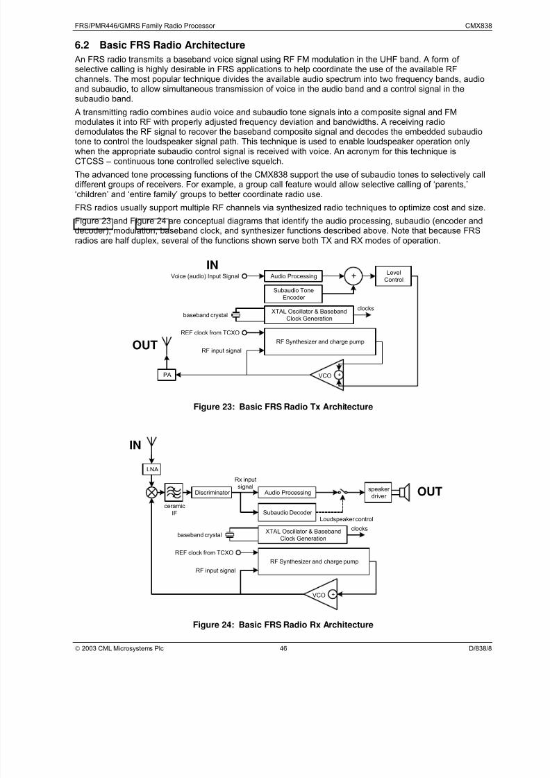
7/29/2019 Radio Gmrs Radio
http://slidepdf.com/reader/full/radio-gmrs-radio 46/72
FRS/PMR446/GMRS Family Radio Processor CMX838
2003 CML Microsystems Plc 46 D/838/8
6.2 Basic FRS Radio Architecture
An FRS radio transmits a baseband voice signal using RF FM modulation in the UHF band. A form of selective calling is highly desirable in FRS applications to help coordinate the use of the available RFchannels. The most popular technique divides the available audio spectrum into two frequency bands, audioand subaudio, to allow simultaneous transmission of voice in the audio band and a control signal in thesubaudio band.
A transmitting radio combines audio voice and subaudio tone signals into a composite signal and FMmodulates it into RF with properly adjusted frequency deviation and bandwidths. A receiving radio
demodulates the RF signal to recover the baseband composite signal and decodes the embedded subaudiotone to control the loudspeaker signal path. This technique is used to enable loudspeaker operation onlywhen the appropriate subaudio control signal is received with voice. An acronym for this technique isCTCSS – continuous tone controlled selective squelch.
The advanced tone processing functions of the CMX838 support the use of subaudio tones to selectively calldifferent groups of receivers. For example, a group call feature would allow selective calling of ‘parents,’‘children’ and ‘entire family’ groups to better coordinate radio use.
FRS radios usually support multiple RF channels via synthesized radio techniques to optimize cost and size.
Figure 23 and Figure 24 are conceptual diagrams that identify the audio processing, subaudio (encoder anddecoder), modulation, baseband clock, and synthesizer functions described above. Note that because FRSradios are half duplex, several of the functions shown serve both TX and RX modes of operation.
Audio ProcessingLevel
Control
RF Synthesizer and charge pump
XTAL Oscillator & BasebandClock Generation
Subaudio ToneEncoder
Voice (audio) Input Signal +
REF clock from TCXO
+VCOPA
clocks
RF input signal
IN
OUT
baseband crystal
Figure 23: Basic FRS Radio Tx Architecture
Discriminator
ceramicIF
LNA
Audio Processing
Rx inputsignal
Subaudio Decoder Loudspeaker control
XTAL Oscillator & BasebandClock Generation
REF clock from TCXO
+VCO
clocks
RF input signal
speaker driver
IN
OUT
RF Synthesizer and charge pump
baseband crystal
Figure 24: Basic FRS Radio Rx Architecture
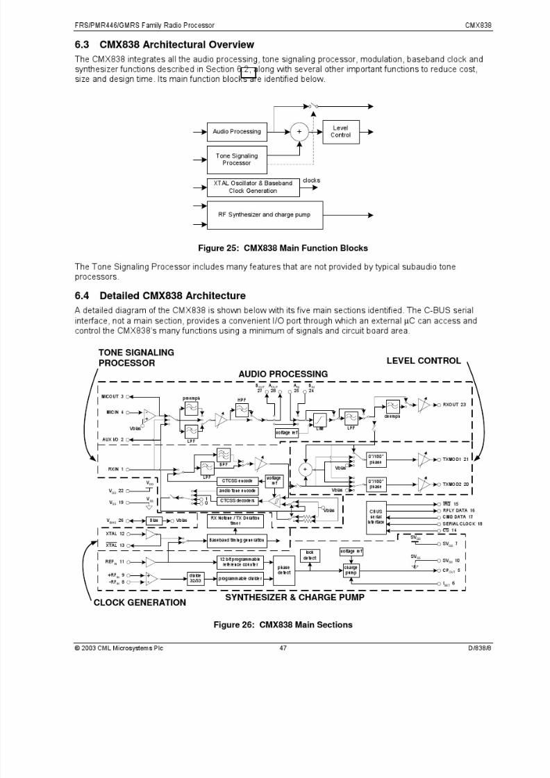
7/29/2019 Radio Gmrs Radio
http://slidepdf.com/reader/full/radio-gmrs-radio 47/72
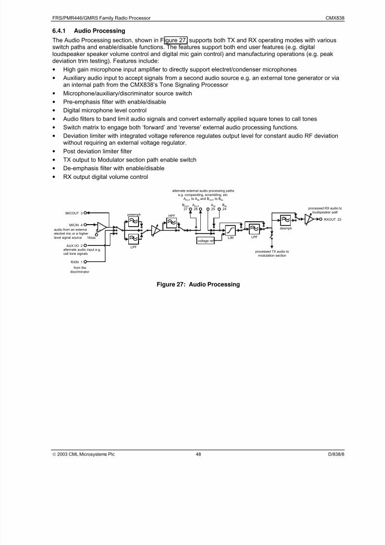
7/29/2019 Radio Gmrs Radio
http://slidepdf.com/reader/full/radio-gmrs-radio 48/72
FRS/PMR446/GMRS Family Radio Processor CMX838
2003 CML Microsystems Plc 48 D/838/8
6.4.1 Audio Processing
The Audio Processing section, shown in Figure 27, supports both TX and RX operating modes with variousswitch paths and enable/disable functions. The features support both end user features (e.g. digitalloudspeaker speaker volume control and digital mic gain control) and manufacturing operations (e.g. peakdeviation trim testing). Features include:
• High gain microphone input amplifier to directly support electret/condenser microphones
• Auxiliary audio input to accept signals from a second audio source e.g. an external tone generator or viaan internal path from the CMX838’s Tone Signaling Processor
• Microphone/auxiliary/discriminator source switch
• Pre-emphasis filter with enable/disable
• Digital microphone level control
• Audio filters to band limit audio signals and convert externally applied square tones to call tones
• Switch matrix to engage both ‘forward’ and ‘reverse’ external audio processing functions.
• Deviation limiter with integrated voltage reference regulates output level for constant audio RF deviationwithout requiring an external voltage regulator.
• Post deviation limiter filter
• TX output to Modulator section path enable switch
• De-emphasis filter with enable/disable
• RX output digital volume control
-
+
Vbias
LPF
preemph HPF
LPFLIMvoltage ref
deemph
MICOUT 3
MICIN 4
AUX I/O 2
RXIN 1
RXOUT 23
AOUT
28BOUT
27 AIN
25BIN
24
processed TX audio tomodulation section
processed RX audio toloudspeaker path
from thediscriminator
audio from an externalelectret mic or a higher level signal source
alternate audio input e.g.call tone signals
alternate external audio processing pathse.g. companding, scrambling, etc.
AOUT to AIN and BOUT to BIN
Figure 27: Audio Processing

7/29/2019 Radio Gmrs Radio
http://slidepdf.com/reader/full/radio-gmrs-radio 49/72

7/29/2019 Radio Gmrs Radio
http://slidepdf.com/reader/full/radio-gmrs-radio 50/72
FRS/PMR446/GMRS Family Radio Processor CMX838
2003 CML Microsystems Plc 50 D/838/8
6.4.2 Tone Signaling Processor
The Tone Signaling Processor, shown in Figure 31, provides a unique combination of features thatoutperforms traditional approaches. It supports traditional subaudio CTCSS tones with advanced, flexible,encode and decode functions to simplify radio designs and enable new FRS radio features. The tonesignaling processor can also generate audio tones suitable for call alert signals to eliminate the need for anexternal tone generator, if desired. Internal signals are exposed via flexible switch paths to support user defined external circuits. Features include:
• 51 parallel CTCSS decoders can be individually enabled/disabled to perform ‘flash’ tone decoding on
user activated tones in an internal tone ‘watch list.’ This architecture provides the performance to supportrapid receive tone scanning, group calling and Tone Cloning™ (automatic CTCSS decoder configuration)end product functions without a decoder response time penalty. Note that one tone must be applied to thedecoders at any given time, consistent with normal CTCSS practice.
• The CTCSS encoder/decoder contains a pre-programmed set of 50 tone definitions. Each tone isreferenced by index for simple application program development. The 50 tone definitions include theentire TIA-603 standard tone set with other common frequencies added. A 51st User Programmable toneallows a user to configure an arbitrary tone frequency.
• Integrated voltage reference regulates CTCSS encoder output level for constant subaudio RF deviationwithout requiring an external voltage regulator.
• Digitally controlled subaudio output level to support various external radio modulation architectures.
• Complete CTCSS decoder status word provides a single Decoder Status bit to directly drive squelch
control decisions in an external µC.
• User configurable CTCSS decoder Notone timer (to adjust CTCSS decoder dropout response),bandwidth (to adjust selectivity) and TX duration timer functions.
• High performance filters with selectable gain controls enhance end product radio sensitivity and supportmultiple design architectures e.g. both internal and external summing of subaudio and audio signals.
• Audio tone generator for call alert signals.
• Controllable switch paths and internal signal exposure to support user developed functions.
LPFCTCSS encode
CTCSS decoders
audio tone encode
voltageref
BPF
Vbias
10
AUX I/O 2
RXIN 1
subaudiooutput
audio calltone output
from thediscriminator
Figure 31: Tone Signaling Processor

7/29/2019 Radio Gmrs Radio
http://slidepdf.com/reader/full/radio-gmrs-radio 51/72
FRS/PMR446/GMRS Family Radio Processor CMX838
2003 CML Microsystems Plc 51 D/838/8
Examples of ‘CTCSS tone decoder’, ‘CTCSS tone encoder’ and ‘internal audio encoder’ paths are illustratedin Figure 32, Figure 33, and Figure 34.
LPFCTCSS encode
CTCSS decoders
audio tone encode
voltageref
BPF
Vbias
10
AUX I/O 2
RXIN 1
subaudiooutput
audio calltone output
from the
discriminator
Tone (Hz)67.069.371.974.477.079.7
...225.7233.6241.8250.3
Decoder Activated
ListYESNONOYESNOYES
...YESNOYESYES
Figure 32: Example CTCSS Tone Decoder Path
LPFCTCSS encode
CTCSS decoders
audio tone encode
voltageref
BPF
Vbias
10
AUX I/O 2
RXIN 1
subaudiooutput
audio calltone output
from the
discriminator
Figure 33: Example CTCSS Tone Encoder Path

7/29/2019 Radio Gmrs Radio
http://slidepdf.com/reader/full/radio-gmrs-radio 52/72
FRS/PMR446/GMRS Family Radio Processor CMX838
2003 CML Microsystems Plc 52 D/838/8
LPFCTCSS encode
CTCSS decoders
audio tone encode
voltageref
BPF
Vbias
10
AUX I/O 2
RXIN 1
subaudiooutput
audio calltone output
from thediscriminator
Figure 34: Example Internal Audio Tone Encoder Path
6.4.3 Level Control
The Level Control section, shown in Figure 35, combines TX audio and subaudio signals using a summer,selectable switch paths, digitally controlled gains, and 0°/180° phase selection to support a variety of radio TXarchitectures.
Synthesized radio transmitters can attenuate subaudio tone levels in a manner related to the subaudio tonefrequency. This section, described below, supports several approaches to manage this aspect of designsbased on synthesizers.
• Use an FM modulator having flat subaudio response. This modulator can be driven by the composite sumof audio and subaudio signals to perform ‘single point modulation.’
• Apply audio signal to the synthesizer VCO input and subaudio signal to the synthesizer referenceoscillator voltage control input. This modulator requires separate audio and subaudio output signals withtheir relative levels trimmed to perform ‘two point modulation.’ Some oscillators are reverse acting and somust have their driving signal inverted before it is applied. Applications requiring summed audio andsubaudio to be applied to both the modulator and synthesizer reference oscillator are also supported.
• Use an FM modulator with attenuating subaudio response. This modulator must be driven by constantaudio levels but subaudio frequency dependent subaudio levels. This driving signal is obtained by varying
the subaudio tone level, according to subaudio tone frequency, and then summing it with the audio signal.
+
Vbias
Vbias
0°/180°phase
0°/180°phase
TXMOD1 21
TXMOD2 20
audiosignal
subaudiosignal
Figure 35: Level Control
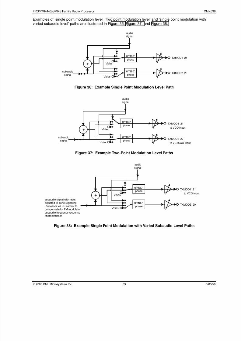
7/29/2019 Radio Gmrs Radio
http://slidepdf.com/reader/full/radio-gmrs-radio 53/72
FRS/PMR446/GMRS Family Radio Processor CMX838
2003 CML Microsystems Plc 53 D/838/8
Examples of ‘single point modulation level’, ‘two point modulation level’ and ‘single point modulation withvaried subaudio level’ paths are illustrated in Figure 36, Figure 37, and Figure 38.
+
Vbias
Vbias
0°/180°phase
0°/180°phase TXMOD1 21
TXMOD2 20
audiosignal
subaudiosignal
Figure 36: Example Single Point Modulation Level Path
+
Vbias
Vbias
0°/180°phase
0°/180°phase
TXMOD1 21
TXMOD2 20
audiosignal
subaudiosignal
to VCO input
to VCTCXO input
Figure 37: Example Two-Point Modulation Level Paths
+
Vbias
Vbias
0°/180°phase
0°/180°phase
TXMOD1 21
TXMOD2 20
audiosignal
to VCO input
subaudio signal with level,adjusted in Tone SignalingProcessor via uC control tocompensate for FM modulator subaudio frequency responsecharacteristics
Figure 38: Example Single Point Modulation with Varied Subaudio Level Paths

7/29/2019 Radio Gmrs Radio
http://slidepdf.com/reader/full/radio-gmrs-radio 54/72
FRS/PMR446/GMRS Family Radio Processor CMX838
2003 CML Microsystems Plc 54 D/838/8
6.4.4 Synthesizer and Charge Pump
The Synthesizer and Charge Pump section reduces component cost and size when compared with non-integrated alternatives. It also provides a simpler programming interface because it is focused on FRSapplications. When combined with an external VCO and related circuits its features include:
• Pre-programmed support for FRS, PMR446 and GMRS RF standard frequencies via simple ‘channelselect’ commands.
• Lock detect function with IRQ indication, if enabled.
• Direct control of synthesizer values for more flexible operation, if desired.• Support for several REFIN reference clock frequencies.
• Charge pump programmed via a combination of a two state internal selection and an external chargecurrent setting resistor.
• Charge pump polarity control via serial command.
• Integrated voltage reference provides constant charge pump current without requiring an external voltageregulator.
12 bit programmablereference counter
+
- programmable divider
divide
32/33
phasedetect
chargepump
lockdetect
voltage ref
REFIN 11
+RFIN 9
-RFIN 8
CPOUT 5
ISET 6
Figure 39: Synthesizer and Charge Pump
6.4.5 Clock Generation
The Clock Generation section develops internal clocks to operate the Audio Processing,Tone Signaling Processor and Level Control sections. The clock source can be externally supplied or internally developed from an external crystal (attached to pins 12 and 13) or from a REFIN clock signal appliedto the Synthesizer & Charge Pump. When the latter is used, the external crystal can be omitted to save costand space. Several crystal and REF IN clock frequencies are supported.
Clock generation also includes a timer that is used in both RX and TX modes. In RX mode it operates as aNotone timer to qualify when a received subaudio tone has been removed. In TX mode it serves to time atransmission’s duration.
Baseband timing generation
RX Notone / TX Durationtimer
XTAL 12
XTAL 13
REFIN
via Synthesizer and Charge Pump section
attachoptionalcrystal
internalclocks
Figure 40: Clock Generation

7/29/2019 Radio Gmrs Radio
http://slidepdf.com/reader/full/radio-gmrs-radio 55/72

7/29/2019 Radio Gmrs Radio
http://slidepdf.com/reader/full/radio-gmrs-radio 56/72
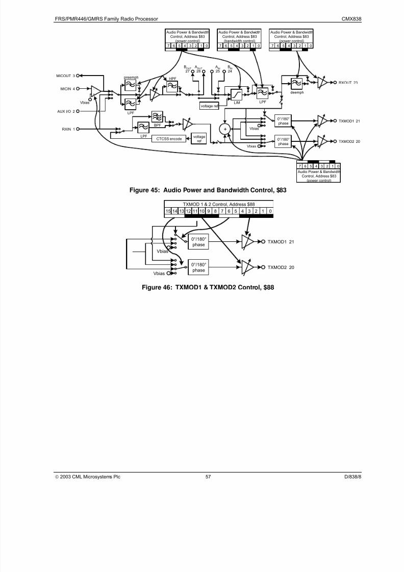
7/29/2019 Radio Gmrs Radio
http://slidepdf.com/reader/full/radio-gmrs-radio 57/72
FRS/PMR446/GMRS Family Radio Processor CMX838
2003 CML Microsystems Plc 57 D/838/8
-
+
Vbias
LPF
preemph HPF
LPFLIM
LPFCTCSS encode
+
Vbias
Vbias
0°/180°phase
0°/180°phase
voltage ref
deemph
voltageref
BPF
MICOUT 3
MICIN 4
AUX I/O 2
RXIN 1
RXOUT 23
TXMOD1 21
TXMOD2 20
AOUT
28B
OUT
27 A
IN
25B
IN
24
7 6 5 4 3 2 1
Audio Power & BandwidthControl, Address $83
(power control)
0
7 6 5 4 3 2 1
Audio Power & BandwidthControl, Address $83
(power control)
0
7 6 5 4 3 2 1
Audio Power & BandwidthControl, Address $83
(power control)
0 7 6 5 4 3 2 1
Audio Power & BandwidthControl, Address $83(bandwidth control)
0
Figure 45: Audio Power and Bandwidth Control, $83
Vbias
Vbias
0°/180°phase
0°/180°phase
TXMOD1 21
TXMOD2 20
015 14 13 12 11 10 9 8 7 6 5 4 3 2 1
TXMOD 1 & 2 Control, Address $88
Figure 46: TXMOD1 & TXMOD2 Control, $88

7/29/2019 Radio Gmrs Radio
http://slidepdf.com/reader/full/radio-gmrs-radio 58/72
FRS/PMR446/GMRS Family Radio Processor CMX838
2003 CML Microsystems Plc 58 D/838/8
6.6 Application Examples
This section includes application examples in the form of ordered C-BUS register lists. When listed, theregister must be read or written to according to its defined type.
6.6.1 CMX838 Initialization
The CMX838’s many sections and functions must be initialized in proper sequence before they can beoperated. This example describes an initialization routine that may be used to configure the device for:
• Baseband clock generation from RF synthesizer clock
• Device digitally controlled amplifiers (DCA) set to normal power operation
• Filters and deviation limiter set for normal power consumption
• Synthesizer enabled and set to FRS channels
• Subaudio section memory cleared and ready for configuration data
6.6.1.1 Register Descriptions:GENERAL RESET ($01)
SYNTHESIZER BASEBAND CLOCK CONTROL ($89): 10010000b = $90• baseband and synthesizer reference clock from REF IN, xtal amp disabled (10)• REF IN frequency 12.8MHz (0100)• Bits 1-0 are don’t cares as xtal is not used
AUDIO POWER AND BANDWIDTH CONTROL ($83): 01010100b = $54• Modulation digitally controlled amplifiers (DCA) and microphone amplifier configured for normal
operation (01)• Audio filters, deviation limiter, and audio level DCA configured for normal operation (01)• De-emphasis network and Rx Audio Out DCA configured for normal operation (01)• Post deviation limiter LPF set to wide setting (0)• Bit 0 is unused (0)
SYNTHESIZER GENERAL CONTROL ($8A): 01010100b = $54
• Synthesizer is enabled (01)• Lock detect IRQ is enabled, status updated every phase comparison when the last two comparisons
disagree (01)
• Magnitude of charge pump current is 40*Iset (0)• Positive VCO gain slope (1)• FRS channels selected (00)
TONE SIGNALING CONTROL ($93): 01001111b = $4F• Enable power (01)• No IRQ (00)• Subaudio processor ‘soft reset’ (1111)
NOTE: Once the subaudio processor is in the ‘soft reset’ mode, any further tasks that are issued to thesubaudio processor will cause it to enter the ‘fast initialization’ mode. In this mode, the tone detectors andencoders do not run. In order to resume normal operation from this ‘fast initialization’ mode, a task of $0 mustbe written to the TONE SIGNALING CONTROL register ($93).
6.6.2 TX, subaudio encoding, single point modulation
This TX scenario configures the CMX838 as shown in F igure 47, f or:• Baseband clock generation from RF synthesizer clock• input from microphone• internal pre-emphasis• HPF used• Limiter/LPF used• De-emphasis bypassed (this configuration will not allow Tx tone to be heard at speaker)• CTCSS encoder enabled• Audio + subaudio tones summed and presented at TX MOD 1 (TX MOD 2 set to Vbias)

7/29/2019 Radio Gmrs Radio
http://slidepdf.com/reader/full/radio-gmrs-radio 59/72
FRS/PMR446/GMRS Family Radio Processor CMX838
2003 CML Microsystems Plc 59 D/838/8
6.6.2.1 Register Descriptions:GENERAL RESET ($01): (if required)
SYNTHESIZER BASEBAND CLOCK CONTROL ($89): 10010000b = $90• baseband and synthesizer reference clock from REF IN, xtal amp disabled (10)• REF IN frequency 12.8MHz (0100)• Bits 1-0 are don’t cares as xtal is not used
SETUP ($80): 11111110b = $FE• Tx Enabled (1)• Audio input supplied by microphone output (11)• Audio signal passed through HPF to limiter (1111)• Bit 0 is unused (0)
AUDIO CONTROL ($81): 00010000b = $10• Audio signal passed through pre-emphasis filter and HPF (000)• Audio level set to 0.0dB (10000)
RX AUDIO LEVEL CONTROL ($82): 00010111b = $17• Deviation limiter not bypassed (0)• Post deviation limiter LPF not bypassed (0)
• De-emphasis network not bypassed (0)• Rx volume control set to 0.0dB (10111)
AUDIO POWER AND BANDWIDTH CONTROL ($83): 01010100b = $54• Modulation digitally controlled amplifiers (DCA) and microphone amplifier configured for normal
operation (01)• Audio filters, deviation limiter, and audio level DCA configured for normal operation (01)• De-emphasis network and Rx Audio Out DCA configured for normal operation (01)• Post deviation limiter LPF set to wide setting (0)• Bit 0 is unused (0)
TX MOD 1 & 2 CONTROL ($88): 00000000 01110000b = $0070• Tx Mod 2 output set to Vbias (000)
• Tx Mod 2 output gain set to off (00000)• Tx Mod 1 output set to Audio + Tone (011)• Tx Mod 1 output gain set to 0.0dB (10000)
SYNTHESIZER GENERAL CONTROL ($8A): 01010100b = $54• Synthesizer is enabled (01)• Lock detect IRQ is enabled, status updated every phase comparison when the last two comparisons
disagree (01)• Magnitude of charge pump current is 40*Iset (0)• Positive VCO gain slope (1)• FRS channels selected (00)
SYNTHESIZER CHANNEL SELECT ($8B): 00000001b = $01• Bits 7 and 6 set to zero (00)• Lock detect comparison window set to +/- 20ns (00)• FRS channel 1 selected (0001)
TONE SIGNALING CONTROL REGISTER ($93): 01001111b = $4F• Enable power (01)• No IRQ (00)• Subaudio processor ‘soft reset’ (1111)
8 BIT SUBAUDIO TASK DATA ($95): 00010000b = $10• Load 110.9Hz tone (00010000)
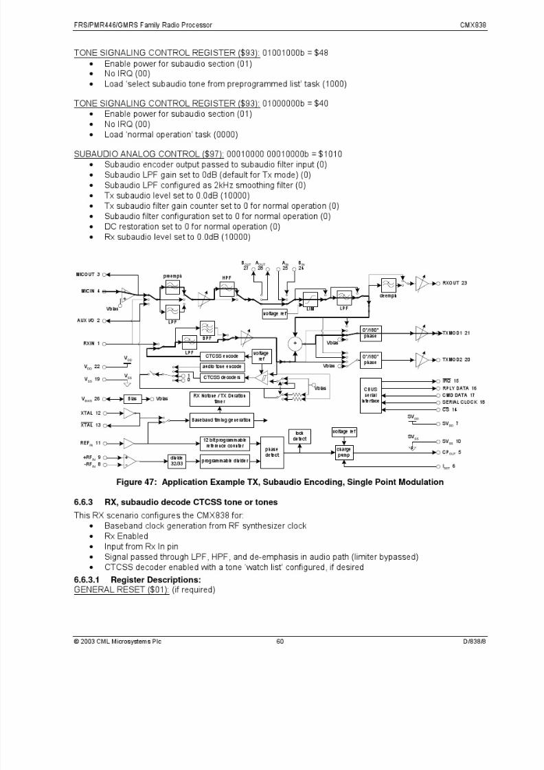
7/29/2019 Radio Gmrs Radio
http://slidepdf.com/reader/full/radio-gmrs-radio 60/72
7/29/2019 Radio Gmrs Radio
http://slidepdf.com/reader/full/radio-gmrs-radio 61/72
FRS/PMR446/GMRS Family Radio Processor CMX838
2003 CML Microsystems Plc 61 D/838/8
SYNTHESIZER BASEBAND CLOCK CONTROL ($89): 10010000b = $90• baseband and synthesizer reference clock from REF IN, xtal amp disabled (10)• REF IN frequency 12.8MHz (0100)
• Bits 1-0 are don’t cares as xtal is not used
SETUP ($80): 00111110b = $3E• Rx Enabled (0)• Audio input signal supplied from RX Input (01)• Audio signal passed through HPF out to limiter (1111)• Bit 0 is unused (0)
AUDIO CONTROL ($81): 01010000b = $50• First stage filtering configured as LPF (01)• Audio signal passed through HPF (0)• Audio level set to 0.0dB (10000)
RX AUDIO LEVEL CONTROL ($82): 11010111b = $D7• Deviation limiter bypassed (1)• Post deviation limiter LPF bypassed (1)• Audio signal passed through de-emphasis network (0)
• Rx volume control set to 0.0dB (10111)
AUDIO POWER AND BANDWIDTH CONTROL ($83): 01010100b = $54• Modulation digitally controlled amplifiers (DCA) and microphone amplifier configured for normal
operation (01)• Audio filters, deviation limiter, and audio level DCA configured for normal operation (01)• De-emphasis network and Rx Audio Out DCA configured for normal operation (01)• Post-deviation limiter LPF set to wide setting (0)• Bit 0 is unused (0)
TX MOD 1 & 2 CONTROL ($88): 00000000 00000000b = $0000• Tx Mod 2 output set to Vbias (000)• Tx Mod 2 output gain set to off (00000)
• Tx Mod 1 output set to Vbias (000)• Tx Mod 1 output gain set to off (00000)
SYNTHESIZER GENERAL CONTROL ($8A): 01010100b = $54• Synthesizer is enabled (01)• Lock detect IRQ is enabled, status updated every phase comparison when the last two comparisons
disagree (01)• Magnitude of charge pump current is 40*Iset (0)• Positive VCO gain slope (1)• FRS channels selected (00)
SYNTHESIZER CHANNEL SELECT ($8B): 00000001b = $01• Bits 7 and 6 set to zero (00)
• Lock detect comparison window set to +/- 20ns (00)• FRS channel 1 selected (0001)
TONE SIGNALING CONTROL ($93): 01001111b = $4F• Enable power (01)• No IRQ (00)• Subaudio processor ‘soft reset’ (1111)
- this task is only required when the subaudio processor is enabled the first time after power up(‘General Reset’ alone does not require the ‘soft reset’ task to be issued)

7/29/2019 Radio Gmrs Radio
http://slidepdf.com/reader/full/radio-gmrs-radio 62/72
FRS/PMR446/GMRS Family Radio Processor CMX838
2003 CML Microsystems Plc 62 D/838/8
8 BIT SUBAUDIO TASK DATA ($95): 10110010b = $B2• Load hex value resulting from $80 logically ordered with $32 (‘254.1Hz tone select’)
10000000b | 00110010b = 10110010b = $B2• When in Rx mode and MSB of $95 is “1”, the desired tone(s) is (are) loaded onto the ‘tone watch list’• When in Rx mode and MSB of $95 is “0”, the desired tone(s) is (are) removed from the ‘tone watch
list’
TONE SIGNALING CONTROL ($93): 01010100b = $54• Enable power for subaudio section (01)• IRQ when detect status change (01)• Load ‘enable/disable tone detector’ task (0100)
IF DESIRED, REPEAT TONE LOADING AND TONE DETECTOR ENABLING STEPS (immediately priortwo steps) TO BUILD A ‘TONE WATCH LIST.’
TONE SIGNALING CONTROL ($93): 01010000b = $50• Enable power for subaudio section (01)• IRQ when detect status change (01)• Load ‘normal operation’ task (0000)
SUBAUDIO ANALOG CONTROL ($97): 00010000 00010000b = $1010• Rx Input passed to subaudio filter input (0)• Subaudio LPF gain set to +20dB (default for Rx mode) (0)• Subaudio LPF configured as 65Hz high pass DC blocking filter (0)• Tx subaudio level set to 0.0dB (10000)• Tx subaudio filter gain counter set to 0 for normal operation (0)• Subaudio filter configuration set to 0 for normal operation (0)• DC restoration set to 0 for normal operation (0)• Rx subaudio level set to 0.0dB (10000)
6.6.4 RX, multiple subaudio tone detect - Tone Cloning™
This RX scenario configures the CMX838 for:• Baseband clock generation from RF synthesizer clock
• Rx Enabled• Input from Rx In pin• Signal passed through LPF, HPF, and de-emphasis in audio path (limiter bypassed)• CTCSS decoder enabled, all TIA-603 standard tones selected for detection (recognition)
Tone Cloning™ is a function that allows one FRS radio to quickly identify and clone the CTCSS tone settingtransmitted by another radio. For end users, Tone Cloning™ simplifies the setup and operation of FRS radiosthe CTCSS tone programming process on the radio’s user interface.
After the CMX838’s TIA-603 standard tone set tone decoders are activated in a tone ‘watch list ’, the CMX838then will promiscuously listen for any of those tones and identify it when it is received. The identity can thenbe used to efficiently set up the CMX838 CTCSS encoder to continue to use that tone.
6.6.4.1 Register Descriptions:GENERAL RESET ($01): (if required)
SYNTHESIZER BASEBAND CLOCK CONTROL ($89): 10010000b = $90• baseband and synthesizer reference clock from REF IN, xtal amp disabled (10)• REF IN frequency 12.8MHz (0100)• Bits 1-0 are don’t cares as xtal is not used
SETUP ($80): 00111110b = $3E• Rx Enabled (0)• Audio input signal supplied from RX Input (01)• Audio signal passed through HPF out to limiter (1111)• Bit 0 is unused (0)
7/29/2019 Radio Gmrs Radio
http://slidepdf.com/reader/full/radio-gmrs-radio 63/72
FRS/PMR446/GMRS Family Radio Processor CMX838
2003 CML Microsystems Plc 63 D/838/8
AUDIO CONTROL ($81): 01010000b = $50• First stage filtering configured as LPF (01)• Audio signal passed through HPF (0)
• Audio level set to 0.0dB (10000)
RX AUDIO LEVEL CONTROL ($82): 11010111b = $D7• Deviation limiter bypassed (1)• Post deviation limiter LPF bypassed (1)• Audio signal passed through deemphasis network (0)• Rx volume control set to 0.0dB (10111)
AUDIO POWER AND BANDWIDTH CONTROL ($83): 01010100b = $54• Modulation digitally controlled amplifiers (DCA) and microphone amplifier configured for normal
operation (01)• Audio filters, deviation limiter, and audio level DCA configured for normal operation (01)• De-emphasis network and Rx Audio Out DCA configured for normal operation (01)• Post deviation limiter LPF set to wide setting (0)• Bit 0 is unused (0)
TX MOD 1 & 2 CONTROL ($88): 00000000 00000000b = $0000
• Tx Mod 2 output set to Vbias (000)• Tx Mod 2 output gain set to off (00000)• Tx Mod 1 output set to Vbias (000)• Tx Mod 1 output gain set to off (00000)
SYNTHESIZER GENERAL CONTROL ($8A): 01010100b = $54• Synthesizer is enabled (01)• Lock detect IRQ is enabled, status updated every phase comparison when the last two comparisons
disagree (01)• Magnitude of charge pump current is 40*Iset (0)• Positive VCO gain slope (1)• FRS channels selected (00)
SYNTHESIZER CHANNEL SELECT ($8B): 00000001b = $01• Bits 7 and 6 set to zero (00)• Lock detect comparison window set to +/- 20ns (00)• FRS channel 1 selected (0001)
TONE SIGNALING CONTROL ($93): 01001111b = $4F• Enable power (01)• No IRQ (00)• Subaudio processor ‘soft reset’ (1111)
this task is only required when the subaudio processor is enabled the first time after power up(‘General Reset’ alone does not require the ‘soft reset’ task to be issued)
8 BIT SUBAUDIO TASK DATA ($95): 10111111b = $BF• Load hex value resulting from $80 logically ordered with $3F (‘all TIA-603 tones select’)
- 10000000b | 00111110b = 10111111b = $BF• When in Rx mode and MSB of $95 is “1”, the desired tone(s) is (are) loaded onto the ‘tone watch list’• When in Rx mode and MSB of $95 is “0”, the desired tone(s) is (are) removed from the ‘tone watch
list’
TONE SIGNALING CONTROL ($93): 01010100b = $54• Enable power for subaudio section (01)• IRQ when detect status change (01)• Load ‘enable/disable tone detector’ task (0100)
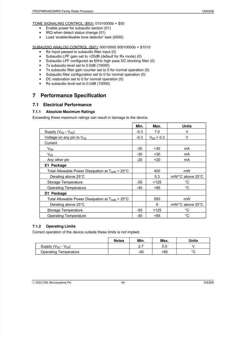
7/29/2019 Radio Gmrs Radio
http://slidepdf.com/reader/full/radio-gmrs-radio 64/72
FRS/PMR446/GMRS Family Radio Processor CMX838
2003 CML Microsystems Plc 64 D/838/8
TONE SIGNALING CONTROL ($93): 01010000b = $50• Enable power for subaudio section (01)• IRQ when detect status change (01)
• Load ‘enable/disable tone detector’ task (0000)
SUBAUDIO ANALOG CONTROL ($97): 00010000 00010000b = $1010• Rx Input passed to subaudio filter input (0)
• Subaudio LPF gain set to +20dB (default for Rx mode) (0)• Subaudio LPF configured as 65Hz high pass DC blocking filter (0)
• Tx subaudio level set to 0.0dB (10000)• Tx subaudio filter gain counter set to 0 for normal operation (0)• Subaudio filter configuration set to 0 for normal operation (0)• DC restoration set to 0 for normal operation (0)• Rx subaudio level set to 0.0dB (10000)
7 Performance Specification
7.1 Electrical Performance
7.1.1 Absolute Maximum Ratings
Exceeding these maximum ratings can result in damage to the device.
Min. Max. Units
Supply (VDD - VSS) -0.3 7.0 V
Voltage on any pin to VSS -0.3 VDD + 0.3 V
Current
VDD -30 +30 mA
VSS -30 +30 mA
Any other pin -20 +20 mA
E1 Package
Total Allowable Power Dissipation at T AMB = 25°C 400 mWDerating above 25°C 5.3 mW/°C above 25°C
Storage Temperature -55 +125 °C
Operating Temperature -40 +85 °C
D1 Package
Total Allowable Power Dissipation at T AMB = 25°C 550 mW
Derating above 25°C 9 mW/°C above 25°C
Storage Temperature -55 +125 °C
Operating Temperature -40 +85 °C
7.1.2 Operating LimitsCorrect operation of the device outside these limits is not implied.
Notes Min. Max. Units
Supply (VDD - VSS) 2.7 5.5 V
Operating Temperature -40 +85 °C
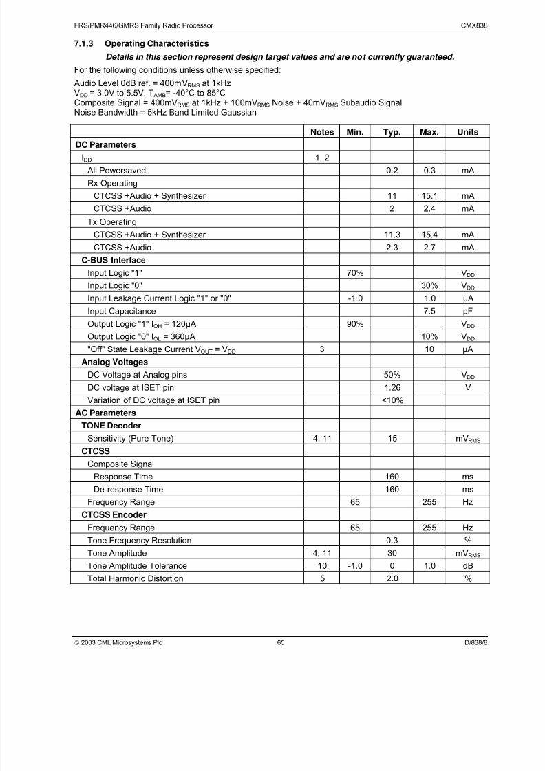
7/29/2019 Radio Gmrs Radio
http://slidepdf.com/reader/full/radio-gmrs-radio 65/72
FRS/PMR446/GMRS Family Radio Processor CMX838
2003 CML Microsystems Plc 65 D/838/8
7.1.3 Operating Characteristics
Details in this section represent design target values and are not currently guaranteed.
For the following conditions unless otherwise specified:
Audio Level 0dB ref. = 400mVRMS at 1kHzVDD = 3.0V to 5.5V, T AMB= -40°C to 85°CComposite Signal = 400mVRMS at 1kHz + 100mVRMS Noise + 40mVRMS Subaudio SignalNoise Bandwidth = 5kHz Band Limited Gaussian
Notes Min. Typ. Max. Units
DC Parameters
IDD 1, 2
All Powersaved 0.2 0.3 mA
Rx Operating
CTCSS +Audio + Synthesizer 11 15.1 mA
CTCSS +Audio 2 2.4 mA
Tx Operating
CTCSS +Audio + Synthesizer 11.3 15.4 mA
CTCSS +Audio 2.3 2.7 mA
C-BUS InterfaceInput Logic "1" 70% VDD
Input Logic "0" 30% VDD
Input Leakage Current Logic "1" or "0" -1.0 1.0 µA
Input Capacitance 7.5 pF
Output Logic "1" IOH = 120µA 90% VDD
Output Logic "0" IOL = 360µA 10% VDD
"Off" State Leakage Current VOUT = VDD 3 10 µA
Analog Voltages
DC Voltage at Analog pins 50% VDD
DC voltage at ISET pin 1.26 VVariation of DC voltage at ISET pin <10%
AC Parameters
TONE Decoder
Sensitivity (Pure Tone) 4, 11 15 mVRMS
CTCSS
Composite Signal
Response Time 160 ms
De-response Time 160 ms
Frequency Range 65 255 Hz
CTCSS EncoderFrequency Range 65 255 Hz
Tone Frequency Resolution 0.3 %
Tone Amplitude 4, 11 30 mVRMS
Tone Amplitude Tolerance 10 -1.0 0 1.0 dB
Total Harmonic Distortion 5 2.0 %
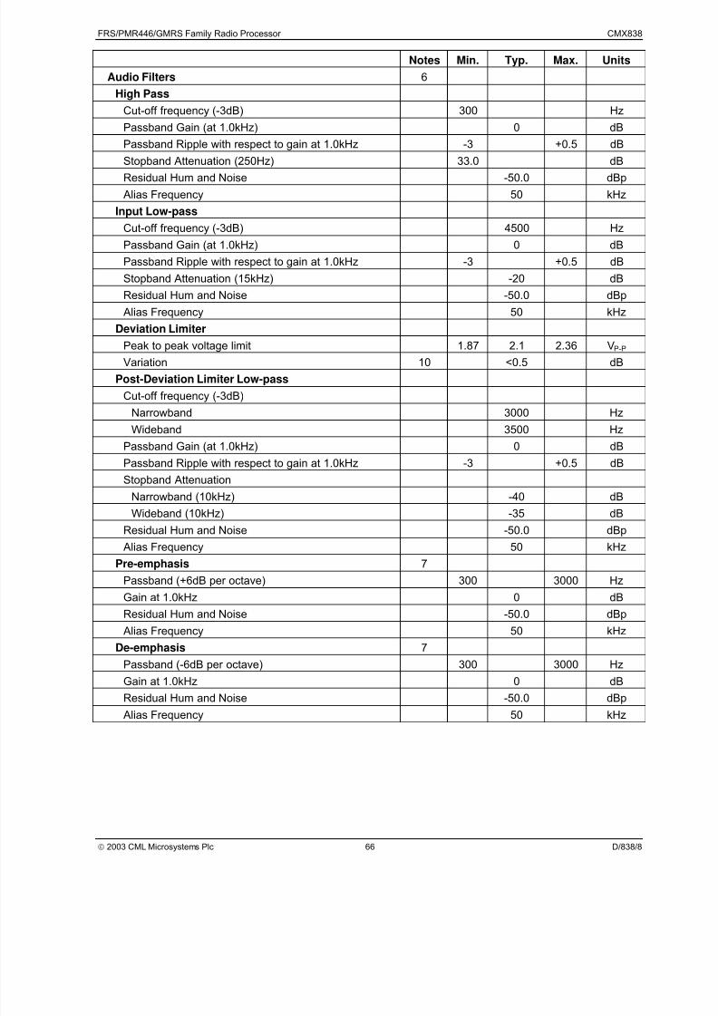
7/29/2019 Radio Gmrs Radio
http://slidepdf.com/reader/full/radio-gmrs-radio 66/72
FRS/PMR446/GMRS Family Radio Processor CMX838
2003 CML Microsystems Plc 66 D/838/8
Notes Min. Typ. Max. Units
Audio Filters 6
High Pass
Cut-off frequency (-3dB) 300 Hz
Passband Gain (at 1.0kHz) 0 dB
Passband Ripple with respect to gain at 1.0kHz -3 +0.5 dB
Stopband Attenuation (250Hz) 33.0 dB
Residual Hum and Noise -50.0 dBp
Alias Frequency 50 kHz
Input Low-pass
Cut-off frequency (-3dB) 4500 Hz
Passband Gain (at 1.0kHz) 0 dB
Passband Ripple with respect to gain at 1.0kHz -3 +0.5 dB
Stopband Attenuation (15kHz) -20 dB
Residual Hum and Noise -50.0 dBp
Alias Frequency 50 kHz
Deviation Limiter
Peak to peak voltage limit 1.87 2.1 2.36 VP-P
Variation 10 <0.5 dB
Post-Deviation Limiter Low-pass
Cut-off frequency (-3dB)
Narrowband 3000 Hz
Wideband 3500 Hz
Passband Gain (at 1.0kHz) 0 dB
Passband Ripple with respect to gain at 1.0kHz -3 +0.5 dB
Stopband Attenuation
Narrowband (10kHz) -40 dB
Wideband (10kHz) -35 dBResidual Hum and Noise -50.0 dBp
Alias Frequency 50 kHz
Pre-emphasis 7
Passband (+6dB per octave) 300 3000 Hz
Gain at 1.0kHz 0 dB
Residual Hum and Noise -50.0 dBp
Alias Frequency 50 kHz
De-emphasis 7
Passband (-6dB per octave) 300 3000 Hz
Gain at 1.0kHz 0 dBResidual Hum and Noise -50.0 dBp
Alias Frequency 50 kHz

7/29/2019 Radio Gmrs Radio
http://slidepdf.com/reader/full/radio-gmrs-radio 67/72
FRS/PMR446/GMRS Family Radio Processor CMX838
2003 CML Microsystems Plc 67 D/838/8
Notes Min. Typ. Max. Units
External Processing Paths
AIN, BIN - Input Impedance 100 kΩ
AOUT, BOUT – Output Impedance 2.0 kΩ
RXIN
Input Impedance 100 kΩ
Auxiliary Input/Output (AUX I/O)
Input Impedance – AUX output disabled 100 kΩ
Output Impedance – AUX output enabled 100 kΩ
Transmitter Modulator Drives
Mod.1 Attenuator
Attenuation at 0dB -0.2 0 0.2 dB
Cumulative Attenuation Error with respect to attenuation at 0dB
-1.0 1.0 dB
Mod.2 Attenuator
Attenuation at 0dB -0.2 0 0.2 dB
Cumulative Attenuation Error
with respect to attenuation at 0dB
-0.6 0.6 dB
Xtal/Clock Input
Pulse Width ('High' or 'Low') 9 40.0 ns
Input Impedance (at 100Hz) 10.0 MΩ
Gain Input = 1mVRMS at 100Hz 20.0 dB
Transmit Input Amplifier (microphone amplifier)
Maximum capacitive load 100 pF
Unity Gain BW (unloaded) 5 MHz
Maximum closed loop gain 40 dB
Slew Rate 1 V/µs
Gain Control Amplifiers: MOD1, MOD2, RXOUTEnabled - Output Swing 8 2.7 VP-P
Disabled - Output Impedance 100 kΩ
Maximum capacitive load 150 pF
Unity Gain BW (unloaded) 2.6 MHz
Slew Rate 2.1 V/µs
RF Synthesizer
RF Input Sensitivity -20 dBm
Minimum Internal Phase Comparison Frequency 6.25 kHz
RF Input Frequency 100 500 MHz
Maximum reference input frequency 25 MHzSinusoidal input voltage (mVRMS) 100 500 mVRMS
Input impedance (real) 100 kΩ
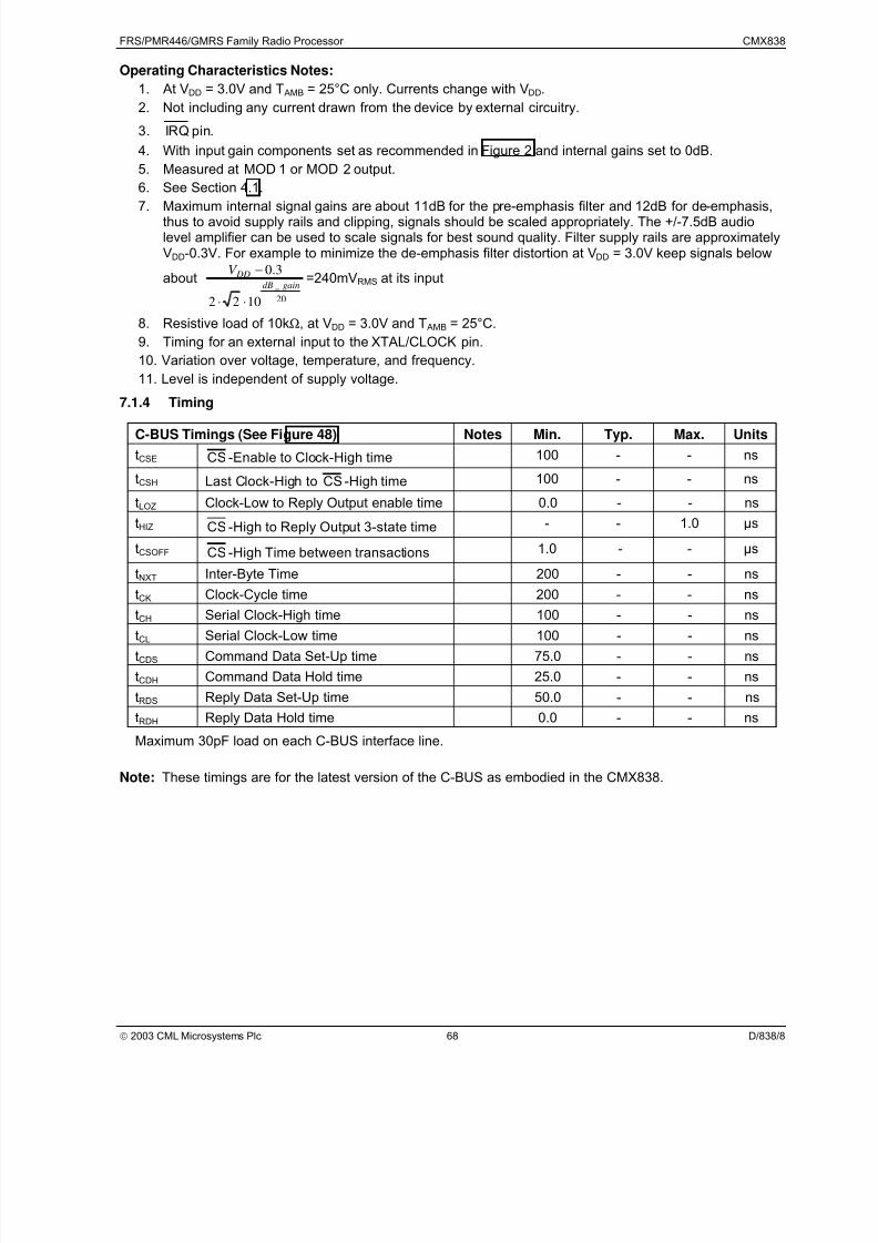
7/29/2019 Radio Gmrs Radio
http://slidepdf.com/reader/full/radio-gmrs-radio 68/72
FRS/PMR446/GMRS Family Radio Processor CMX838
2003 CML Microsystems Plc 68 D/838/8
Operating Characteristics Notes:
1. At VDD = 3.0V and T AMB = 25°C only. Currents change with VDD.
2. Not including any current drawn from the device by external circuitry.
3. IRQ pin.
4. With input gain components set as recommended in Figure 2 and internal gains set to 0dB.
5. Measured at MOD 1 or MOD 2 output.
6. See Section 4.1.
7. Maximum internal signal gains are about 11dB for the pre-emphasis filter and 12dB for de-emphasis,thus to avoid supply rails and clipping, signals should be scaled appropriately. The +/-7.5dB audiolevel amplifier can be used to scale signals for best sound quality. Filter supply rails are approximatelyVDD-0.3V. For example to minimize the de-emphasis filter distortion at VDD = 3.0V keep signals below
about
20
_
1022
3.0gaindB
DDV
⋅⋅
−=240mVRMS at its input
8. Resistive load of 10kΩ, at VDD = 3.0V and T AMB = 25°C.
9. Timing for an external input to the XTAL/CLOCK pin.
10. Variation over voltage, temperature, and frequency.
11. Level is independent of supply voltage.
7.1.4 Timing
C-BUS Timings (See Figure 48) Notes Min. Typ. Max. Units
tCSE CS -Enable to Clock-High time 100 - - ns
tCSH Last Clock-High to CS -High time 100 - - ns
tLOZ Clock-Low to Reply Output enable time 0.0 - - ns
tHIZ CS -High to Reply Output 3-state time - - 1.0 µs
tCSOFF CS -High Time between transactions 1.0 - - µs
tNXT Inter-Byte Time 200 - - ns
tCK Clock-Cycle time 200 - - ns
tCH Serial Clock-High time 100 - - ns
tCL Serial Clock-Low time 100 - - ns
tCDS Command Data Set-Up time 75.0 - - ns
tCDH Command Data Hold time 25.0 - - ns
tRDS Reply Data Set-Up time 50.0 - - ns
tRDH Reply Data Hold time 0.0 - - ns
Maximum 30pF load on each C-BUS interface line.
Note: These timings are for the latest version of the C-BUS as embodied in the CMX838.

7/29/2019 Radio Gmrs Radio
http://slidepdf.com/reader/full/radio-gmrs-radio 69/72
FRS/PMR446/GMRS Family Radio Processor CMX838
2003 CML Microsystems Plc 69 D/838/8
CS
HI-Z
= Level not important or undefined
SERIAL CLOCK
tCSE tCK
tCL
tCDS tRDS
tCDH tRDH
70% VDD30% VDD
tCH tCK
tCSH
tLOZ
COMMAND DATA
COMMANDDATA
SERIALCLOCK
REPLYDATA
REPLY DATA
7 6 5 4 3 2 1 0 7 6 5 4 3 2 1 0
7 6 5 4 3 2 1 0
tNXT
tCSOFF
tHIZ
Figure 48: C-BUS Timing
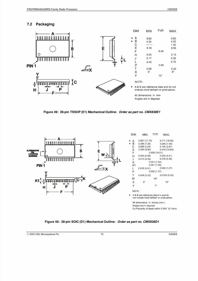
7/29/2019 Radio Gmrs Radio
http://slidepdf.com/reader/full/radio-gmrs-radio 70/72
FRS/PMR446/GMRS Family Radio Processor CMX838
2003 CML Microsystems Plc 70 D/838/8
7.2 Packaging
Figure 49: 28-pin TSSOP (E1) Mechanical Outline: Order as part no. CMX838E1
Figure 50: 28-pin SOIC (D1) Mechanical Outline: Order as part no. CMX838D1
7/29/2019 Radio Gmrs Radio
http://slidepdf.com/reader/full/radio-gmrs-radio 71/72
FRS/PMR446/GMRS Family Radio Processor CMX838
Handling precautions: This product includes input protection, however, precautions should be taken toprevent device damage from electro-static discharge. CML does not assume any responsibility for theuse of any circuitry described. No IPR or circuit patent licences are implied. CML reserves the right atany time without notice to change the said circuitry and this product specification. CML has a policy of testing every product shipped using calibrated test equipment to ensure compliance with this productspecification. Specific testing of all circuit parameters is not necessarily performed.
www.cmlmicro.com
For FAQs see: www.cmlmicro.com/products/faqs/
For a full data sheet listing see: www.cmlmicro.com/products/datasheets/download.htm
For detailed application notes: www.cmlmicro.com/products/applications/
Oval Park, Langford,Maldon, Essex,CM9 6WG - England.
Tel: +44 (0)1621 875500
Fax: +44 (0)1621 875600
Sales:[email protected]
Technical Support:
4800 Bethania Station Road,Winston-Salem,NC 27105 - USA.
Tel: +1 336 744 5050,800 638 5577
Fax: +1 336 744 5054
Sales:[email protected]
Technical Support:
No 2 Kallang PuddingRoad, #09 to 05/06 MactechIndustrial Building,Singapore 349307
Tel: +65 6745 0426
Fax: +65 6745 2917
Sales:[email protected]
Technical Support:
No. 218, Tian Mu RoadWest, Tower 1, Unit 1008,Shanghai Kerry EverbrightCity, Zhabei,Shanghai 200070,China.
Tel: +86 21 6317 4107+86 21 6317 8916
Fax: +86 21 6317 0243
Sales:[email protected]
Technical Support:

7/29/2019 Radio Gmrs Radio
http://slidepdf.com/reader/full/radio-gmrs-radio 72/72
This datasheet has been downloaded from:
www.DatasheetCatalog.com
Datasheets for electronic components.