Radio frequency and analog CMOS integrated circuit design ...rx9189351/... · adoption of low-power...
114
1 Radio Frequency and Analog CMOS Integrated Circuit Design Methods for Low-Power Medical Devices with Wireless Connectivity A Dissertation Presented by CHUN-HSIANG CHANG To The Department of ELECTRICAL AND COMPUTER ENGINEERING in partial fulfillment of the requirements for the degree of Doctor of Philosophy in the field of ELECTRICAL ENGINEERING Northeastern University Boston, Massachusetts November 2015
Transcript of Radio frequency and analog CMOS integrated circuit design ...rx9189351/... · adoption of low-power...

1
Radio Frequency and Analog CMOS Integrated Circuit Design
Methods for Low-Power Medical Devices with Wireless Connectivity
A Dissertation Presented
by
CHUN-HSIANG CHANG
To
The Department of ELECTRICAL AND COMPUTER ENGINEERING
in partial fulfillment of the requirements
for the degree of
Doctor of Philosophy
in the field of
ELECTRICAL ENGINEERING
Northeastern University
Boston, Massachusetts
November 2015
2
Abstract
The ongoing improvements of complementary metal-oxide semiconductor
(CMOS) technologies are enabling the integration of an increasing number of analog and
digital circuits into single chips, which is a trend that continuous to result in performance
enhancements and smaller portable electronic devices with wireless connectivity. A
major challenge is that the radio frequency (RF) front-end section consumes excessive
power in many new battery-powered wireless devices. For this reason, it is essential to
create novel analog circuit design methods with significant power reductions for short-
range communication applications.
In this dissertation, linearity enhancement techniques for analog RF front-ends
are proposed and demonstrated with a subthreshold low-noise amplifier (LNA) and an
active down-conversion mixer. The linearization methods involve extra passive compo-
nents to accomplish partial cancellation of third-order nonlinearity products, thereby
reducing the distortion caused by subthreshold biasing to enable more widespread
adoption of low-power design techniques. A 1.8GHz LNA was designed and fabricated
with 0.11µm CMOS technology to prove the concepts. Test chip measurement results
reveal that the linearized low-power LNA has a 15.2 dB voltage gain, a 3.8dB noise
figure, and a -3.7dBm third-order intermodulation intercept point (IIP3) with a power
consumption of 0.336mW. Another 2.1GHz LNA fabricated in 0.13µm CMOS technol-
ogy has a 9dB voltage gain, a 5.8dB noise figure, and a 0dBm IIP3 with a power
consumption of 0.3mW. A linearized low-power RF receiver frond-end (LNA and
mixer) was also fabricated in 0.11µm CMOS technology and evaluated with measure-
ments. This 1.95 GHz RF front-end has 20.6dB voltage gain, a 6dB double-side band
noise figure and a -10.8dBm IIP3 with a power consumption of 0.9mW.
Another product of this research is an input impedance boosting method that was
developed for long-term monitoring of electroencephalography (EEG) signals. An
instrumentation amplifier (IA) having a power consumption of 93.6μW in 0.13μm
CMOS technology was designed with a negative capacitance generation technique to
3
cancel the adverse effects of input capacitances from the electrode cables and printed
circuit boards. The IA with negative capacitance generation feedback (NCGFB) does not
consume any extra power to boost the measured impedance from below 40MΩ to above
500MΩ at 50Hz after proper adjustment of its digitally programmable capacitors when
the equivalent capacitance at the input is 150pF. Based on simulation and measurement
results, the important instrumentation amplifier performance parameters are not signifi-
cantly affected by addition of the proposed input capacitance cancellation technique.

4
Acknowledgements
First and foremost, I would like to thank my dissertation advisor, Prof. Marvin
Onabajo, for his guidance and support throughout these past four and half years. I would
also like to thank my committee members, Prof. Yong-Bin Kim and Prof. Nian X. Sun,
for their guidance through the final stages of my Ph.D. degree completion; especially
Prof. Kim who made some of the chip fabrications possible with his support and mentor-
ship.
I would like to thank Li Xu and Kainan Wang who assisted me to measure the
RF chips and discussed the results with me on numerous occasions. I want to thank
Alireza Zahrai, Li Xu, and Kainan Wang for collaborating on the SCAFELAB project.
Without their hard work, I could not have completed the input impedance boosting
technique for EEG applications. I also thank Hari Chauhan, In-Seok Jung, and Yongsuk
Choi for working together on an RF built-in testing project.
I thank the National Science Foundation for financial support of the research
projects under awards #1349692 and #1451213.
Finally, to my wife, Shih-wei, thank you for encouragement and support. With-
out you, I could not have finished my Ph.D. study.

5
Table of Contents
1. Introduction ................................................................................................................ 12
1.1 Overview of design requirements in emerging applications ............................ 12
1.2 Low-power RF front-end circuit design challenges ......................................... 14
1.3 Analog circuit design challenges in EEG front-ends ....................................... 15
1.4 Contributions of this research .......................................................................... 16
2. Subthreshold RF Circuit Analysis and Design Considerations ................................. 17
2.1 gm/ID methodology ........................................................................................... 17
2.1.1 Contribution and distribution of parasitic capacitances ....................... 18
2.1.2 Nonlinearity analysis ............................................................................ 19
2.2 Volterra series analysis .................................................................................... 20
2.2.1 Common-source amplifier small-signal model .................................... 21
2.2.2 Common-gate amplifier small-signal model ........................................ 22
3. Linearization of Low-Power RF Frond-End Circuits ................................................ 24
3.1 Input impedance matching optimization for low-power low-noise amplifiers 24
3.1.1 LNA input impedance analysis and tuning method ............................. 25
3.1.2 Simulation results ................................................................................. 30
3.1.3 Conclusions .......................................................................................... 37
3.2 Proposed low-noise amplifier design techniques ............................................. 38
3.2.1 Analysis and design of the linearized LNA ......................................... 40
3.2.2 LNA measurement results .................................................................... 47
3.2.3 Conclusion ........................................................................................... 58
3.3 Proposed mixer design techniques ................................................................... 59
3.3.1 Analysis and design of a linearized mixer ........................................... 59
3.3.2 Mixer simulation results ....................................................................... 66

6
3.3.3 RF front-end measurement results ....................................................... 70
3.3.4 Conclusion ........................................................................................... 77
4. Analog Frond-End Circuits for Brain Signal Acquisitions with Dry Electrodes ...... 78
4.1 System-level considerations ............................................................................. 78
4.2 Instrumentation amplifier ................................................................................. 80
4.2.1 Instrumentation amplifier small-signal model analysis ....................... 82
4.2.2 Negative capacitance generation feedback analysis ............................ 86
4.3 IA simulation results ........................................................................................ 87
4.4 EEG front-end measurement results ................................................................ 93
4.4.1 IA gain measurement results ................................................................ 93
4.4.2 Input impedance measurement results ................................................. 99
4.5 Conclusion ..................................................................................................... 101
5. General Conclusion and Future Work ..................................................................... 102
6. Appendices .............................................................................................................. 103
6.1 Appendix A .................................................................................................... 103
6.2 Appendix B .................................................................................................... 104
6.3 Appendix C .................................................................................................... 105
6.4 Appendix D .................................................................................................... 105
7. References ................................................................................................................ 107
7
List of Figures
Figure 1. WBAN example for medical applications. ...................................................... 13
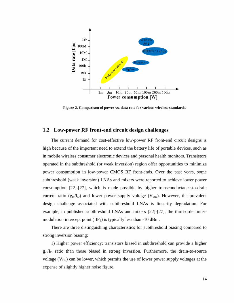
Figure 2. Comparison of power vs. data rate for various wireless standards. ................. 14
Figure 3. Basic performance evaluation setup for an NMOS device. ............................. 17
Figure 4. Drain current (ID) with logarithmic scale and current efficiency (gm/ID) vs.
overdrive voltage (VOV). .................................................................................................. 18
Figure 5. Contribution of parasitic capacitances to the total gate capacitance (Cgg) vs.
gm/ID ................................................................................................................................. 19
Figure 6. Transition frequency (fT) vs. gm/ID. .................................................................. 19
Figure 7. Normalized 2nd-order and 3rd-order transconductance characteristics of an
NMOS device. .................................................................................................................. 20
Figure 8. (a) CS amplifier, (b) nonlinear small-signal model of a CS amplifier. ............ 22
Figure 9. (a) CG amplifier, (b) nonlinear small-signal model of a CG amplifier. ........... 23
Figure 10. Conventional cascode LNA with inductive source degeneration. ................. 26
Figure 11. Small-signal model of transistor M2............................................................... 27
Figure 12. Simplified small-signal model of transistor M2. ............................................ 27
Figure 13. A general model of the Miller effect related to transistor M1. ....................... 28
Figure 14. Simplified equivalent circuit of Figure 10. .................................................... 28
Figure 15. Schematic of the n-bit capacitor network for S11 compensation. ................... 30
Figure 16. Input impedance matching comparison between conventional and proposed
equations for different operating regions. ........................................................................ 32
Figure 17. Input impedance matching comparison between conventional and proposed
equations for different transconductance values of M1. .................................................. 32
Figure 18. Layout of the reference LNA. ........................................................................ 35
Figure 19. Layout of the tunable LNA. ........................................................................... 35
Figure 20. Linearized subthreshold LNA. ....................................................................... 39
Figure 21. Digitally-programmable capacitor (Cgd2_ext) for linearity tuning. .................. 39
Figure 22. Nonlinear small-signal model of the LNA’s input stage with M1.................. 41
Figure 23. Nonlinear small-signal model of the LNA’s cascode stage with M2. ............ 42

8
Figure 24. (a) Simulated voltage gain from Vin to Vx of the LNA with and without Lg2
and Cgd2_ext (ideal components), and (b) calculated results of |ε(Δω,2ω)| for Lg2 with
three Cgd2_ext combinations in the cascode stage (with M2). ............................................ 44
Figure 25. Simplified small-signal model for reverse isolation analysis of transistor M2.
......................................................................................................................................... 47
Figure 26. Chip micrograph of the fabricated linearized subthreshold LNA in Dongbu
0.11µm CMOS technology. ............................................................................................. 49
Figure 27. LNA PCB with IIP3 tuning functionality. ..................................................... 49
Figure 28. Setup for S-parameter measurements. ............................................................ 50
Figure 29. Two-tone test setup. ....................................................................................... 50
Figure 30. Setup for noise measurement. ........................................................................ 51
Figure 31. Measured scattering parameters of the linearized LNA with buffer (5.9dB
loss). ................................................................................................................................. 53
Figure 32. Measured noise figure of the linearized LNA with buffer. ............................ 53
Figure 33. (a) Measured IIP3 of the linearized LNA with buffer, (b) output spectrum
from a test with two tones at 1.8 GHz and 1.7995 GHz and an input power of -35 dBm.
......................................................................................................................................... 54
Figure 34. Measured 1-dB compression point of the linearized LNA with buffer at 1.8
GHz. ................................................................................................................................. 55
Figure 35. Linearized subthreshold LNA in IBM 0.13µm CMOS technology (a)
schematic, and (b) chip micrograph. ................................................................................ 56
Figure 36. IIP3 vs. Cgd2_ext comparison (simulation vs. measurement results). ............... 58
Figure 37. Proposed linearized subthreshold mixer. ....................................................... 61
Figure 38. Small-signal model of the linearized mixer. .................................................. 62
Figure 39. (a) Equivalent half-circuit of the small-signal model in Figure 38, (b)
simplified small-signal model. ......................................................................................... 62
Figure 40. Nonlinear small-signal model of the mixer’s transconductance stage. .......... 64
Figure 41. Example evaluation: |ε(Δω,2 ω)| vs. L1 for different values of Cc. ................ 64
Figure 42. Small-signal model for conversion gain analysis. .......................................... 66
Figure 43. Layout of the linearized mixer. ...................................................................... 68
Figure 44. Output spectrum from a simulation with -30 dBm input power. ................... 69

9
Figure 45. IIP3 curve (typical corner case in Table 9). ................................................... 69
Figure 46. Simulated mixer IIP3 and voltage gain vs. LO power (typical corner case in
Table 9). ........................................................................................................................... 70
Figure 47. Schematic of the linearized subthreshold RF front-end. ................................ 71
Figure 48. Chip micrograph of the fabricated linearized subthreshold RF front-end in
Dongbu 0.11µm CMOS technology. ............................................................................... 71
Figure 49. PCB for RF front-end testing. ........................................................................ 72
Figure 50. Block diagram of the RF front-end measurement setup. ............................... 72
Figure 51. Measured S11 of the RF front-end. ................................................................ 74
Figure 52. Measured NFDSB of the RF front-end (IF = 10 MHz). ................................... 74
Figure 53. (a) Measured IIP3 of the RF front-end with balun (9.5dB loss), (b) output
spectrum from a test with two tones at 10 MHz and 12 MHz and an input power of -36.5
dBm. ................................................................................................................................. 75
Figure 54. Measured 1-dB compression point of the RF front-end with input and output
baluns (at IF = 10 MHz). ................................................................................................. 76
Figure 55. Measured output amplitude before the output balun. ..................................... 76
Figure 56. Basic negative impedance converter (NIC), where Zin = -Z when R1 = R2. ... 78
Figure 57. Analog front-end for EEG signal measurements with electrode cable
capacitances and calibration blocks for input impedance boosting. ................................ 79
Figure 58. Current injection with the test current generator. ........................................... 80
Figure 59. (a) Instrumentation amplifier (IA) with direct current feedback and negative
capacitance generation feedback (NCGFB); (b) variable R2 implementation; (c) input
biasing circuitry. .............................................................................................................. 81
Figure 60. (a) Small-signal model of the IA’s input and feedback stages; (b) small-signal
model of the IA’s output stage. ........................................................................................ 85
Figure 61. Negative capacitance generation feedback (NCGFB) with programmable
capacitors between nodes vi+ and vC (and nodes vi- and vD). ........................................... 87
Figure 62. Voltage swings at the IA input with current injection from the OTA for two
cases: i.) with NCGFB, ii.) without NCGFB. (Noise was activated during the transient
simulations based on the integrated noise density from 0.01Hz to 100Hz.) ................... 87
10
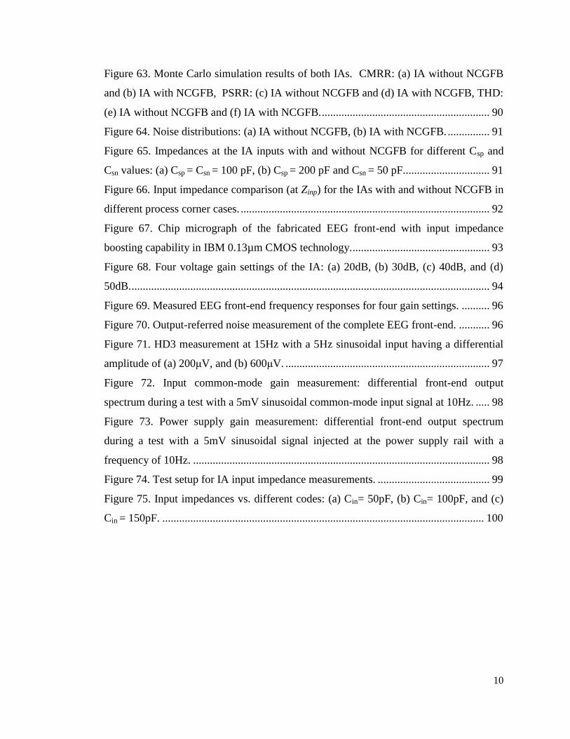
Figure 63. Monte Carlo simulation results of both IAs. CMRR: (a) IA without NCGFB
and (b) IA with NCGFB, PSRR: (c) IA without NCGFB and (d) IA with NCGFB, THD:
(e) IA without NCGFB and (f) IA with NCGFB. ............................................................ 90
Figure 64. Noise distributions: (a) IA without NCGFB, (b) IA with NCGFB. ............... 91
Figure 65. Impedances at the IA inputs with and without NCGFB for different Csp and
Csn values: (a) Csp = Csn = 100 pF, (b) Csp = 200 pF and Csn = 50 pF. .............................. 91
Figure 66. Input impedance comparison (at Zinp) for the IAs with and without NCGFB in
different process corner cases. ......................................................................................... 92
Figure 67. Chip micrograph of the fabricated EEG front-end with input impedance
boosting capability in IBM 0.13µm CMOS technology. ................................................. 93
Figure 68. Four voltage gain settings of the IA: (a) 20dB, (b) 30dB, (c) 40dB, and (d)
50dB. ................................................................................................................................ 94
Figure 69. Measured EEG front-end frequency responses for four gain settings. .......... 96
Figure 70. Output-referred noise measurement of the complete EEG front-end. ........... 96
Figure 71. HD3 measurement at 15Hz with a 5Hz sinusoidal input having a differential
amplitude of (a) 200μV, and (b) 600μV. ......................................................................... 97
Figure 72. Input common-mode gain measurement: differential front-end output
spectrum during a test with a 5mV sinusoidal common-mode input signal at 10Hz. ..... 98
Figure 73. Power supply gain measurement: differential front-end output spectrum
during a test with a 5mV sinusoidal signal injected at the power supply rail with a
frequency of 10Hz. .......................................................................................................... 98
Figure 74. Test setup for IA input impedance measurements. ........................................ 99
Figure 75. Input impedances vs. different codes: (a) Cin= 50pF, (b) Cin= 100pF, and (c)
Cin = 150pF. ................................................................................................................... 100

11
List of Tables
Table 1 Summary of popular low-power wireless standards ........................................... 13
Table 2. Design parameters of the reference LNA and tunable LNA ............................. 34
Table 3. Post-layout simulation – comparison of the reference LNA and tunable LNA at
2.4 GHz ............................................................................................................................ 36
Table 4. Tunable LNA performance comparison with other published results ............... 37
Table 5. Linearized subthreshold LNA design parameters ............................................. 48
Table 6. Comparison of LNA measurement results ........................................................ 57
Table 7. Gain and third-order intermodulation distortion of the subthreshold LNA in
IBM 0.13µm CMOS technology for all linearity tuning settings .................................... 58
Table 8. Mixer design parameters ................................................................................... 68
Table 9. Simulation results with fRF1 = 2.4 GHz, fRF2 = 2.398 GHz, and fLO = 2.41 GHz
for process corner cases (VDD = 0.6V) ............................................................................ 69
Table 10. Comparison of mixer designs .......................................................................... 70
Table 11. RF front-end design parameters ...................................................................... 73
Table 12. Comparison of low-power RF front-ends ........................................................ 77
Table 13. Parameters of the IA designs in IBM 0.13μm CMOS technology without and
with NCGFB .................................................................................................................... 89
Table 14. Comparison of instrumentation amplifier simulation results .......................... 89

12
1. Introduction
The ongoing improvements of complementary metal-oxide semiconductor
(CMOS) processing technologies are enabling the integration of an increasing number of
analog and digital circuits into single chips, which is a trend that continuous to result in
performance enhancements and smaller portable electronic devices with wireless con-
nectivity. A major challenge is that radio frequency (RF) front-end modules often
consume more than 60% of the power budget in transceivers [1]. Therefore, it is not only
necessary to develop wireless standards for low-power short-range communication
applications, but also to create novel analog circuit design methods with significant
power reductions.
1.1 Overview of design requirements in emerging applications
Many kinds of low-power wireless standards and circuit design approaches have
been developed for low-rate wireless personal area network (WPAN) or wireless body
area network (WBAN) applications [2]-[22]. These standards include IEEE 802.15.4,
IEEE 802.15.6, Bluetooth low energy (BLE), Near Field Communication (NFC), and
Global Positioning System (GPS). The applications of low-power wireless standards
include health monitoring, fitness, payment, and smart home applications. Figure 1
illustrates a WBAN scenario as an example of remote medical monitoring. In this
application, patients could use implantable or wearable biomedical sensors with wireless
connectivity to upload their health information to doctors immediately [6]-[9].
Table 1 summarizes the key parameters for BLE, IEEE 802.15.4, and IEEE
802.15.6 for the physical layer [4], [11]. As shown in Figure 2, the required power
consumption of the WBAN devices is lower than other existing wireless standards [6].
From Table 1 and Figure 2, low-data rate wireless standards have two key characteris-
tics, which are low-power consumption and short communication distance.

13
Figure 1. WBAN example for medical applications.
Table 1 Summary of popular low-power wireless standards
BLE IEEE 802.15.4 IEEE 802.15.6
Frequency range 2.4-2.4835GHz
2.4GHz/
868MHz/
915MHz
2.4-2.2483GHz/
2.36-2.4GHz(US)/
(400/868/915/950MHz)
Data rate 1 Mbps 20 kbps up to 250 kbps 75.9 kbps up to 971.4
kbps
Network size Undefined Up to 65536 devices Up to 256 devices
Range 10-75 m 10-100 m 2-5 m
14
Figure 2. Comparison of power vs. data rate for various wireless standards.
1.2 Low-power RF front-end circuit design challenges
The current demand for cost-effective low-power RF front-end circuit designs is
high because of the important need to extend the battery life of portable devices, such as
in mobile wireless consumer electronic devices and personal health monitors. Transistors
operated in the subthreshold (or weak inversion) region offer opportunities to minimize
power consumption in low-power CMOS RF front-ends. Over the past years, some
subthreshold (weak inversion) LNAs and mixers were reported to achieve lower power
consumption [22]-[27], which is made possible by higher transconductance-to-drain
current ratio (gm/ID) and lower power supply voltage (VDD). However, the prevalent
design challenge associated with subthreshold LNAs is linearity degradation. For
example, in published subthreshold LNAs and mixers [22]-[27], the third-order inter-
modulation intercept point (IIP3) is typically less than -10 dBm.
There are three distinguishing characteristics for subthreshold biasing compared to
strong inversion biasing:
1) Higher power efficiency: transistors biased in subthreshold can provide a higher
gm/ID ratio than those biased in strong inversion. Furthermore, the drain-to-source
voltage (VDS) can be lower, which permits the use of lower power supply voltages at the
expense of slightly higher noise figure.

15
2) The change of the contribution and increase of parasitic capacitances: In sub-
threshold, the gate-to-source capacitance (Cgs) no longer dominates, implying that the
gate-to-drain capacitance (Cgd) and the gate-to-bulk capacitance (Cgb) have to be taken
into account for more sophisticated design. Moreover, to achieve similar transconduct-
ance gains as in strong inversion it is required to increase the transistor widths, which
results in higher parasitic capacitances and lower transition frequency (fT).
3) Linearity degradation due to highly positive g3/g1: The sign of g3 changes from
negative to positive when the transistor biasing is changed from strong inversion to
subthreshold. In addition, the value of g3/g1 strongly depends on the gm/ID ratio (where
gm = g1) when biasing transistors in the subthreshold region.
1.3 Analog circuit design challenges in EEG front-ends
Battery-powered portable or implantable biopotential and bioimpedance measurement
devices are becoming increasingly widespread in the medical diagnostics field. The
signal acquisitions of the main biosignal-sensing applications such as electroencephalog-
raphy (EEG) and electrocardiography (ECG) involve voltage measurements from a few
microvolts to several millivolts [28]-[30]. Biopotentials are conventionally acquired
using electrodes covered with electrolyte gels or solutions to decrease the contact
impedance at the skin interface to values below 10 KΩ. However, wet-contact measure-
ments cause discomfort and dry out in novel long-term monitoring applications such as
in brain-computer interfaces where EEG signals are acquired and analyzed over hours or
longer [31].
In general, dry electrodes such as inexpensive Ag/AgCl are better suited for long-
term monitoring, but their use is associated with increased contact resistances that can be
above 1 MΩ [32]. This characteristic complicates the measurement of small biopoten-
tials in the range of a few microvolts for EEG applications by requiring very high input
impedance at the analog front-end amplifier of at least 500 MΩ [33]. Nevertheless, a
significant problem is that this impedance is affected by parasitic capacitances of the
integrated circuit package as well as electrode cable and printed circuit board (PCB)
capacitances that could be as high as 50-200 pF at the input of an instrumentation
amplifier (IA). For instance, when the goal is to record EEG signals with frequencies up

16
to 100 Hz, an interface capacitance of 200 pF would limit the input impedance at 100 Hz
to approximately 8 MΩ, which is much less than 500 MΩ and would cause excessive
attenuation such that the EEG signal cannot be measured reliably.
1.4 Contributions of this research
This dissertation summarizes two main research efforts. In the first part, lineariza-
tion techniques for RF front-end circuits are introduced with digital tuning features to
provide compatibility with built-in test and calibration approaches, such as the one
developed at Northeastern University with Fourier fast transform (FFT) engines [34]-
[35]. Novel linearization methods for LNAs and mixers biased in subthreshold have
been demonstrated without additional power consumption to overcome the linearity
deficiency. In addition, digitally programmable elements have also been proposed to
counteract the sensitivity to manufacturing process variations. A test chip with a sub-
threshold LNA has been fabricated in Dongbu 0.11µm CMOS technology and measured
to demonstrate the feasibility of the design technique. To obtain additional measurement
results for the proof of concept, a mixer has been fabricated in Dongbu 0.11µm CMOS
technology, and another LNA in IBM 0.13µm CMOS technology.
In the second project, an input impedance boosting technique for instrumentation
amplifiers was created, which together with an on-chip test signal generator shows
promise to enable long-term brain signal measurements. The instrumentation amplifier
was integrated into an analog EEG front-end with on-chip calibration designed by other
research group members. This prototype chip was verified with measurements to con-
clude this dissertation work.
The organization of this dissertation is as follows. The analyses of normalized para-
sitic capacitances and nonlinearity coefficients based on the gm/ID methodology are
presented in Chapter 2. The nonlinear small-signal models for common source (CS) and
common gate (CG) amplifiers are also derived in Chapter 2 using Volterra series analy-
sis. Novel linearization techniques for subthreshold LNAs and mixers are proposed in
Chapter 3. The input impedance boosting method is presented in Chapter 4. Conclusions
and future work are given in Chapter 5.
17
2. Subthreshold RF Circuit Analysis and Design Considerations
In this dissertation, the gm/ID methodology is applied for the normalized estima-
tions of parasitic capacitances and nonlinearity coefficients [36]. Using the Volterra
series approach, the nonlinear small-signal model is analyzed to derive the three-order
nonlinearity products under consideration of the memory effects from capacitances and
inductances.
2.1 gm/ID methodology
Consider the NMOS device configuration in Figure 3, where the drain-to-source
voltage (VDS) is fixed and equal to VDD/2, and the overdrive voltage (VOV = VGS - Vth,
where VGS is the gate-to-source voltage and Vth is the threshold voltage) is a variable. In
this chapter, a 0.13µm CMOS technology and a minimum length are used in evaluations.
Based on Figure 3, the basic information about gm, ID, and parasitic capacitances (Cgs,
Cgd, and Cgb) can be extracted by sweeping VOV from the subthreshold region to the
strong inversion region. As shown in Figure 4, the current efficiency (gm/ID) decreases
when the bias point changes from the subthreshold region to the strong inversion region.
Accordingly, it is a possible option to use circuits biased in the subthreshold region to
save power. In the following analyses, the gm/ID ratio is also employed as a design
reference for parasitics and nonlinearity coefficients.
Figure 3. Basic performance evaluation setup for an NMOS device.

18
Figure 4. Drain current (ID) with logarithmic scale and current efficiency (gm/ID) vs. overdrive
voltage (VOV).
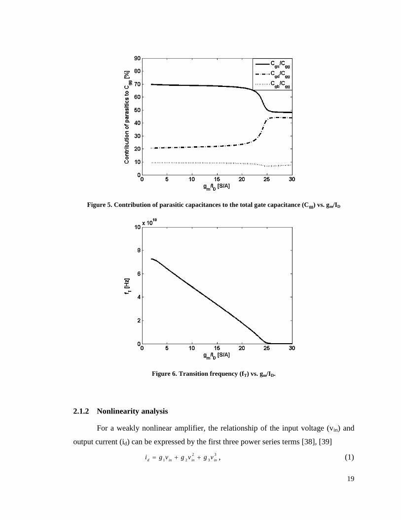
2.1.1 Contribution and distribution of parasitic capacitances
As visualized in Figure 5, the simulated Cgs/Cgg (Cgg = Cgs + Cgd + Cgb) ratio de-
creases approximately 20% when gm/ID is swept such that the bias point changes from
the strong inversion region to the subthreshold region. As a result, Cgs no longer domi-
nates in the subthreshold region. Hence, the gate-drain capacitance Cgd and the gate-bulk
capacitance Cgb should be taken into account for precise input impedance matching
calculation and linearity estimation. In addition, Figure 6 shows that the transition
frequency fT changes from 70 GHz to a few GHz when the transistor bias is varied from
the strong inversion to the subthreshold region. In the past, transistors biased in sub-
threshold region were not seriously considered for analog or RF circuit design because fT
was severely limited [37]. However, new CMOS process technologies have significantly
improved fT values, which has made it possible to design subthreshold circuits with
operating frequencies up to several gigahertz.
19
Figure 5. Contribution of parasitic capacitances to the total gate capacitance (Cgg) vs. gm/ID
Figure 6. Transition frequency (fT) vs. gm/ID.
2.1.2 Nonlinearity analysis
For a weakly nonlinear amplifier, the relationship of the input voltage (vin) and
output current (id) can be expressed by the first three power series terms [38], [39]
3
3
2
21 ininindvgvgvgi , (1)
20
where g1, g2 and g3 are the linear gain, second-order nonlinear coefficient and third-order
nonlinearity coefficient of the amplifier, respectively. Notice that these parameters can
be obtained by taking derivatives of ID with respect to VGS at the DC bias point:
GS
D
V
Ig
1 , 2
2
2!2
1
GS
V
Ig D
,
3
3
3!3
1
GS
V
Ig D
. (2)
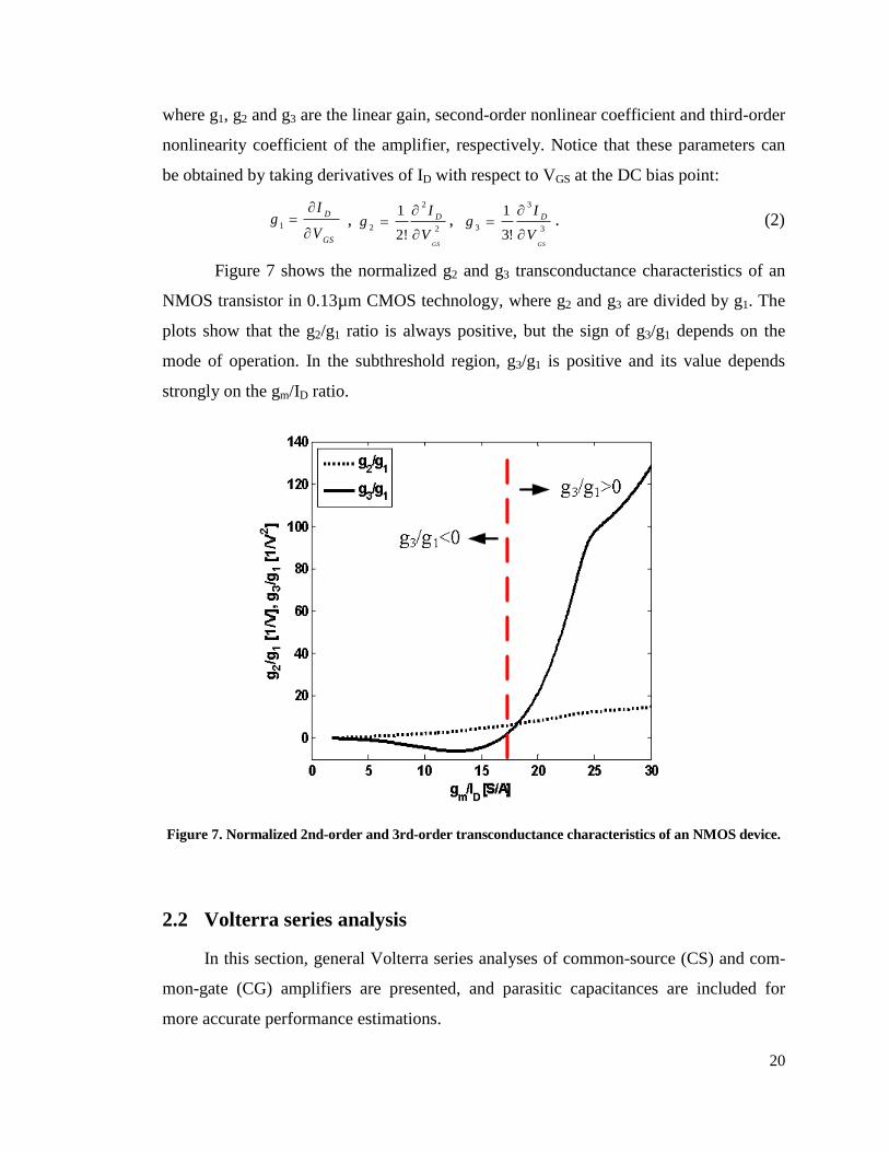
Figure 7 shows the normalized g2 and g3 transconductance characteristics of an
NMOS transistor in 0.13µm CMOS technology, where g2 and g3 are divided by g1. The
plots show that the g2/g1 ratio is always positive, but the sign of g3/g1 depends on the
mode of operation. In the subthreshold region, g3/g1 is positive and its value depends
strongly on the gm/ID ratio.
Figure 7. Normalized 2nd-order and 3rd-order transconductance characteristics of an NMOS device.
2.2 Volterra series analysis
In this section, general Volterra series analyses of common-source (CS) and com-
mon-gate (CG) amplifiers are presented, and parasitic capacitances are included for
more accurate performance estimations.

21
2.2.1 Common-source amplifier small-signal model
Figure 8 shows the CS amplifier and its nonlinear small-signal model, where im-
pedance Z1 is part of the input matching network, Z2 is the source-degeneration
impedance, and Z3 is the impedance connected to the drain of the transistor. RS is the
resistance of the signal source Vx. The third-order intermodulation intercept point of the
transistor can be derived after Volterra series analysis [40]-[42] as
2,6
1
3
1
3
AHRIIP
s
, (3)
where ω is the center frequency of the two intermodulation tones at ωRF1 and ωRF2, Δω is
defined as |ωRF1 - ωRF2|, and Rs is the source resistance (that often is 50Ω). H1(ω) is the
third-order nonlinearity transfer function from Vin to the drain-source current (id), A11(ω)
is the linear transfer function from the input voltage (Vx) to the gate-to-source voltage
(Vgs), and ε(Δω,2ω) represents the nonlinear contribution from the second-order and
third-order terms. Minimization of the term |ε(Δω,2ω)| in (3) leads to improved IIP3.
Here, the analysis of the ε(Δω,2ω) term is focused on the CS and CG amplifier stages
because they are commonly used in the RF amplifier configurations of interest, as
demonstrated by the example designs in this dissertation. The ε(Δω,2ω) term of the CS
amplifier can be expressed as
oB
gg 3
2, , (4)
where
2
12
3
2
11
2
2gggg
ggoB
, (5)
Z
ZZCjCj
ZZCjZZCj
ggdgb
gsgd
13
1131
]1[
][][1
, (6)
323121
2132]1[
ZZZZZZCj
ZZZCjCjZZ
gd
gdgb
, (7)
is
ZRZ 1
, (8)
More detailed derivations are included in Appendix A.

22
Figure 8. (a) CS amplifier, (b) nonlinear small-signal model of a CS amplifier.
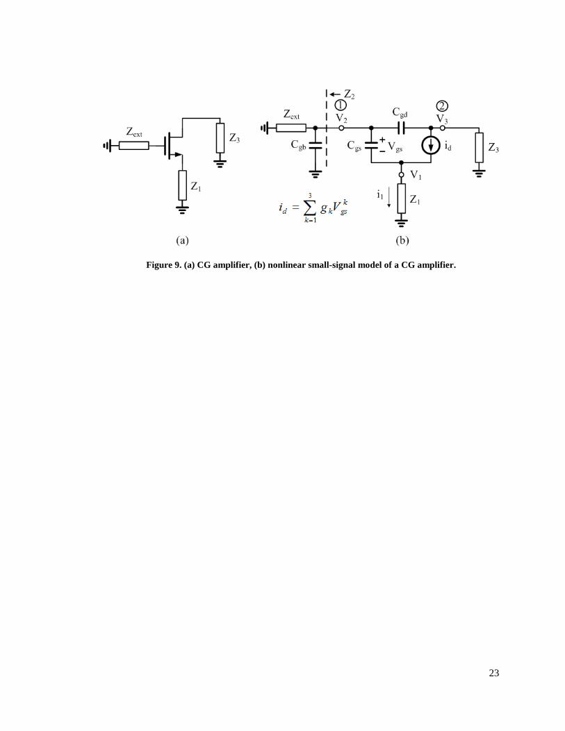
2.2.2 Common-gate amplifier small-signal model
Figure 9 depicts a CG amplifier and its nonlinear small-signal model, where Zext
represents bonding parasitics or an equivalent linearized component. Note that Z1 in this
case models the impedance of the signal source at the source of the transistor. The
following equations give insights into the linearity of the CG amplifier. Using Volterra
series [42] analysis, the amplitude at the third-order intermodulation intercept point
(AIIP3) of the CG amplifier can be derived as
2,
1
3
4
3
1
2
IIP3
AHA . (9)
The definition of ε(Δω,2ω) is the same as in (3) and can be rewritten as
oB
gg 3
2, , (10)
where
2
12
3
2
11
2
2gggg
ggoB
, (11)
32
32
2
23
3
2
]1[
1
ZZCj
ZZCC
ZZCjCjCj
ZCj
g
gd
gdgs
gdgdgs
gd
M
, (12)
ext
gb
ZCj
Z_2
//1
. (13)
The linear transfer function A1(ω) in equation (9) is derived in Appendix B.
23
Figure 9. (a) CG amplifier, (b) nonlinear small-signal model of a CG amplifier.

24
3. Linearization of Low-Power RF Frond-End Circuits
Perpetual progress with integration of voice, video and internet features on chips is
a hallmark of the information age that requires small low-power integrated circuits.
Portable wireless devices continue to be more prevalent in our lives so that vital situa-
tions depend on reliable operation of integrated circuits. Consequently, there is an
increasing incentive to incorporate self-test and correction features to improve reliability
of wireless devices. This is especially true in medical and military applications where
life-saving information is transmitted and received. Although new technologies allow the
design of smaller chips with more functionality, their manufacturing process variability
and post-production aging effects pose growing design and test challenges. Therefore,
the development of adaptive single-chip systems is essential for high reliability in
modern nanometer complementary metal-oxide-semiconductor (CMOS) technology. For
this reason, the analog circuit and design techniques introduced in this dissertation
include the use of digitally tunable elements to enable on-chip calibrations after fabrica-
tions of the chips.
The most widely used IIP3 improvement methods for RF frond-end circuits in nar-
rowband applications can be broadly divided into three categories. The first common
approach is to use the negative feedback topology that can reduce IIP3 by a factor of
(1+T0)3/2
, where T0 is the linear open-loop gain if g2 ≈ 0 [39]-[40]. The second method is
to use one or two auxiliary transistors biased in the weak inversion region to cancel the
third-order nonlinearity coefficient (g3), but the main transistor has to be operated in
strong inversion with higher linear transconductance (g1 = gm) than in the auxiliary path
[39]-[41]. The third way is to operate the main transistor between the moderate inversion
and subthreshold regions for finding the optimum bias zone [40], [63]. However, lineari-
zation methods have not yet been reported with measurements of RF amplifiers using
only transistors biased in the subthreshold region.
3.1 Input impedance matching optimization for low-power low-noise
amplifiers
Handheld battery-powered consumer products with wireless connectivity such as
cellular phones, wireless medical monitoring devices, and global positioning system

25
(GPS) receiver units continue to require power consumption reductions. Emerging
receiver applications in wireless sensor networks, wireless body area networks [43]-
[44], and energy harvesting impose even more stringent demands on the permissible
power dissipation. Furthermore, many reported built-in test and calibration approaches
rely heavily on digital signal processor resources to achieve more robust “digitally-
assisted” analog circuits [46]-[50]. For such applications, the construction of analog
circuits with features for performance tuning is needed. A significant aspect of emerging
variation-resilient design methods is that bias voltages or currents are generated with
digital-to-analog converters or programmable elements, which can be utilized to improve
the reliability of nanometer CMOS systems-on-a-chip [51]. Previously reported digital-
ly-assisted performance boosting techniques have targeted various blocks in the receiver
path, for which a few examples are the tuning of transconductance values in baseband
filters [52], third-order linearity in baseband filters [53], second-order linearity of mixers
[54], and gain of low-noise amplifiers (LNAs) [55].
3.1.1 LNA input impedance analysis and tuning method
3.1.1.1 Derivation of equations for impedance matching
The input impedance of the conventional cascode LNA in Figure 10 can be de-
rived as [56]
)(1
)(
11
1resonanceatL
CLLj
C
gLZ
sT
gs
gs
gs
m
sin
, (14)
where ωT = gm1/Cgs1 is the transition frequency and the coupling capacitor CB is omitted
under the assumption that its value is large.
The real part of the input impedance can be expressed under consideration of the
gate-drain capacitance [56]:
)(21
]Re[
1
1
gs
gd
sT
sin
C
C
LRZ
, (15)
where Rs is the input voltage source (e.g., antenna) resistance to which Re[Zin] should be
matched.
26
In this work, the following additional parameters were considered to analyze the
input impedance: Cgd (parasitic gate-drain capacitance), Cgb (parasitic gate-bulk capaci-
tance), Cds (parasitic drain-source capacitance), ro (small-signal drain-source resistance),
gmb (body effect transconductance), and rg (gate resistance). The small-signal equivalent
circuit of transistor M2 is displayed in Figure 11. To simplify the impedance analysis at
the source terminal of M2, the small-signal model can be modified as in Figure 12 when
the value of rg2 is relatively small. Cgd2M ≈ Cgd2 in Figure 12 is the output Miller capaci-
tance, while Cgb2 and the input Miller capacitance of Cgd2 at the gate have been removed
because they are grounded at both terminals when rg2 is negligible. Thus, the impedance
at the source terminal of M2 can be written as
))(1(
22222
22
2
omgsDo
Do
MZGsCZZ
ZZZ
, (16)
where:
2
22
1//
ds
oosC
rZ , 2
22
1//
gd
DDsC
ZZ
, L
ddDsC
sLRZ1
////2
, and mbm
mggG 2
2 .
M1
M2
Ls
Ld Rd
vout
Cd
RBIAS
LgCBRS
vin
ID
MB
IBIAS
Figure 10. Conventional cascode LNA with inductive source degeneration.
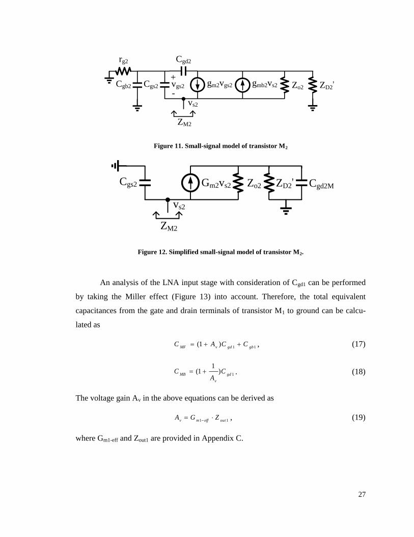
27
gm2vgs2 Zo2
Cgd2
Cgs2
ZM2
rg2
Cgb2 ZD2’+
-vgs2 gmb2vs2
vs2
Figure 11. Small-signal model of transistor M2
Gm2vs2 Zo2Cgs2
ZM2
ZD2’
vs2
Cgd2M
Figure 12. Simplified small-signal model of transistor M2.
An analysis of the LNA input stage with consideration of Cgd1 can be performed
by taking the Miller effect (Figure 13) into account. Therefore, the total equivalent
capacitances from the gate and drain terminals of transistor M1 to ground can be calcu-
lated as
11)1(
gbgdvMFCCAC , (17)
1)
11(
gd
v
MBC
AC . (18)
The voltage gain Av in the above equations can be derived as
11 outeffmvZGA
, (19)
where Gm1-eff and Zout1 are provided in Appendix C.

28
Cgd1
-Av
CMF CMB
Figure 13. A general model of the Miller effect related to transistor M1.
gm1vgs1 Zo1Cgs1
rg1
CMFZM2
Ls
gmb1vs1
CMB
Zin’
Lg
Zin
vgs1
+
- vs1
Figure 14. Simplified equivalent circuit of Figure 10.
A complete analysis of the input impedance Zin gives
MF
ingginsC
ZrsLZ1
//1
. (20)
Typically, Zo1 (Figure 14) and Zo2 (Figure 12) are significantly larger than the
other impedances in the small-signal models under consideration. Assuming that Zo1 and
Zo2 are at least one order of magnitude larger than the related impedances, the following
approximations can be made:
2
2
1
m
MG
Z , (21)
1
111
11
2
1
1))(1(
gd
gsmbms
mbgssm
effmsC
sCggsL
gCLsgG
, (22)

29
1
21
1//
gd
MoutsC
ZZ , (23)
1
1
1
' 1
gs
m
ss
gs
inC
gLsL
sCZ . (24)
At resonance, Ls should be selected properly such that the real term of Zin’ is equal
to Rs - rg1.Voltage gain Av is a complex number, which complicates hand calculations. A
Matlab script to calculate Ls and Lg is provided in Appendix D. Note that off-chip
bonding wire and package parasitics were excluded from the analysis for simplicity, but
the equations could be adapted to include them. Nonetheless, the equations are intended
to aid the initial design and optimizations rather than to replace comprehensive circuit
simulations with models for off-chip parasitics.
3.1.1.2 S11 tuning capability
Tuning of input impedance matching is desirable to compensate for manufacturing
process variations. Such as other on-chip S11 built-in test [57] and self-calibration [58]
methods, the proposed input impedance tuning method is particular for the LNA block.
However, the digitally-assisted tuning feature to be discussed in this section can also be
utilized as part of a system-level calibration that is controlled by the digital signal
processor of an integrated receiver.
Based on the presented input matching equations, a S11-tunable circuit using an
n-bit metal-insulator-metal (MIM) capacitor network (shown in Figure 15) can be
implemented to optimize the input impedance matching under the influence of varia-
tions. Node G1 in Figure 15 is connected to the gate terminal of transistor M1 in Figure
10. After this modification, the input impedance Zin with capacitance CMIM can be
expressed as
)1
////(1
1
MF
ing
MIM
ginsC
ZrsC
sLZ
, (25)
where CMIM is the contribution of the n-bit MIM capacitor. Note that the digitally-
assisted tuning of CMIM allows direct compensation of the effective input Miller capaci-
tance CMF in equations (17) and (20), which is more sensitive to variations of parasitic
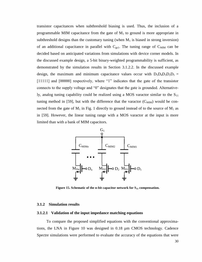
30
transistor capacitances when subthreshold biasing is used. Thus, the inclusion of a
programmable MIM capacitance from the gate of M1 to ground is more appropriate in
subthreshold designs than the customary tuning (when M1 is biased in strong inversion)
of an additional capacitance in parallel with Cgs1. The tuning range of CMIM can be
decided based on anticipated variations from simulations with device corner models. In
the discussed example design, a 5-bit binary-weighted programmability is sufficient, as
demonstrated by the simulation results in Section 3.1.2.2. In the discussed example
design, the maximum and minimum capacitance values occur with D5D4D3D2D1 =
[11111] and [00000] respectively, where “1” indicates that the gate of the transistor
connects to the supply voltage and “0” designates that the gate is grounded. Alternative-
ly, analog tuning capability could be realized using a MOS varactor similar to the S11
tuning method in [59], but with the difference that the varactor (CMIM) would be con-
nected from the gate of M1 in Fig. 1 directly to ground instead of to the source of M1 as
in [59]. However, the linear tuning range with a MOS varactor at the input is more
limited than with a bank of MIM capacitors.
D1D2Dn
G1
MD1MD2MDn
CMIM1CMIM2CMIMn
...
Figure 15. Schematic of the n-bit capacitor network for S11 compensation.
3.1.2 Simulation results
3.1.2.1 Validation of the input impedance matching equations
To compare the proposed simplified equations with the conventional approxima-
tions, the LNA in Figure 10 was designed in 0.18 µm CMOS technology. Cadence
Spectre simulations were performed to evaluate the accuracy of the equations that were
31
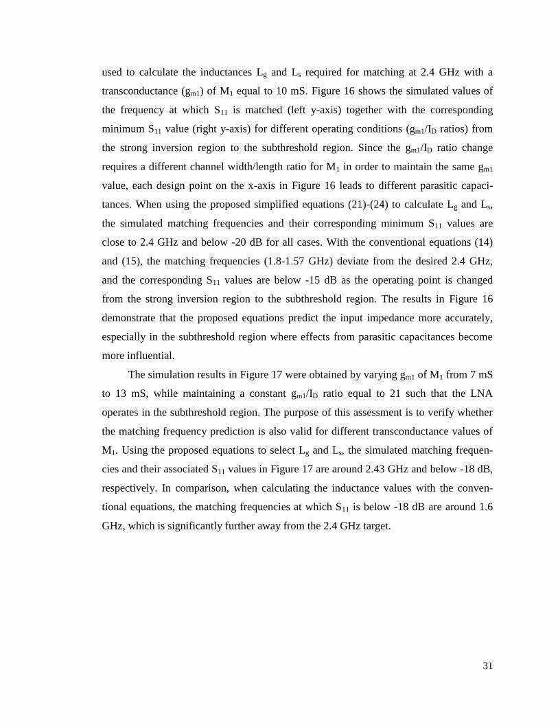
used to calculate the inductances Lg and Ls required for matching at 2.4 GHz with a
transconductance (gm1) of M1 equal to 10 mS. Figure 16 shows the simulated values of
the frequency at which S11 is matched (left y-axis) together with the corresponding
minimum S11 value (right y-axis) for different operating conditions (gm1/ID ratios) from
the strong inversion region to the subthreshold region. Since the gm1/ID ratio change
requires a different channel width/length ratio for M1 in order to maintain the same gm1
value, each design point on the x-axis in Figure 16 leads to different parasitic capaci-
tances. When using the proposed simplified equations (21)-(24) to calculate Lg and Ls,
the simulated matching frequencies and their corresponding minimum S11 values are
close to 2.4 GHz and below -20 dB for all cases. With the conventional equations (14)
and (15), the matching frequencies (1.8-1.57 GHz) deviate from the desired 2.4 GHz,
and the corresponding S11 values are below -15 dB as the operating point is changed
from the strong inversion region to the subthreshold region. The results in Figure 16
demonstrate that the proposed equations predict the input impedance more accurately,
especially in the subthreshold region where effects from parasitic capacitances become
more influential.
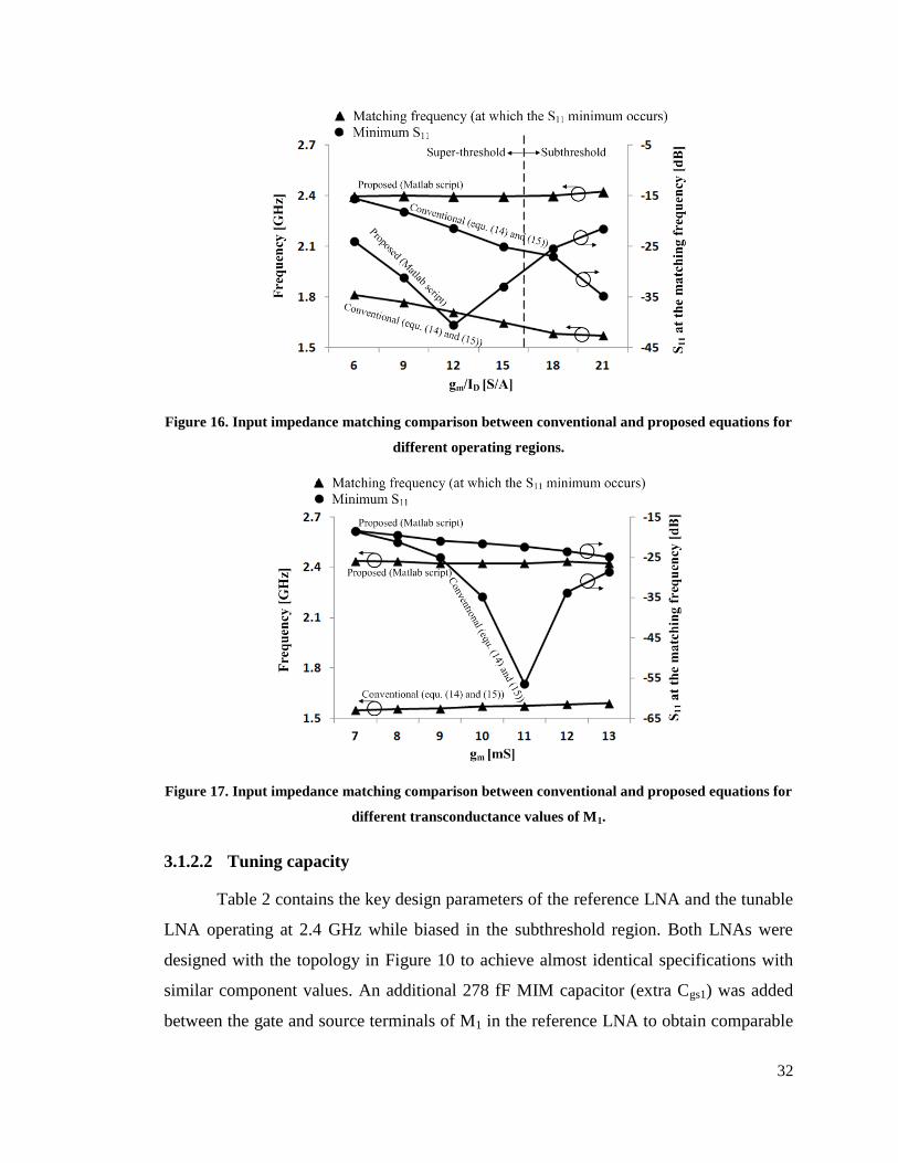
The simulation results in Figure 17 were obtained by varying gm1 of M1 from 7 mS
to 13 mS, while maintaining a constant gm1/ID ratio equal to 21 such that the LNA
operates in the subthreshold region. The purpose of this assessment is to verify whether
the matching frequency prediction is also valid for different transconductance values of
M1. Using the proposed equations to select Lg and Ls, the simulated matching frequen-
cies and their associated S11 values in Figure 17 are around 2.43 GHz and below -18 dB,
respectively. In comparison, when calculating the inductance values with the conven-
tional equations, the matching frequencies at which S11 is below -18 dB are around 1.6
GHz, which is significantly further away from the 2.4 GHz target.
32
Figure 16. Input impedance matching comparison between conventional and proposed equations for
different operating regions.
Figure 17. Input impedance matching comparison between conventional and proposed equations for
different transconductance values of M1.
3.1.2.2 Tuning capacity
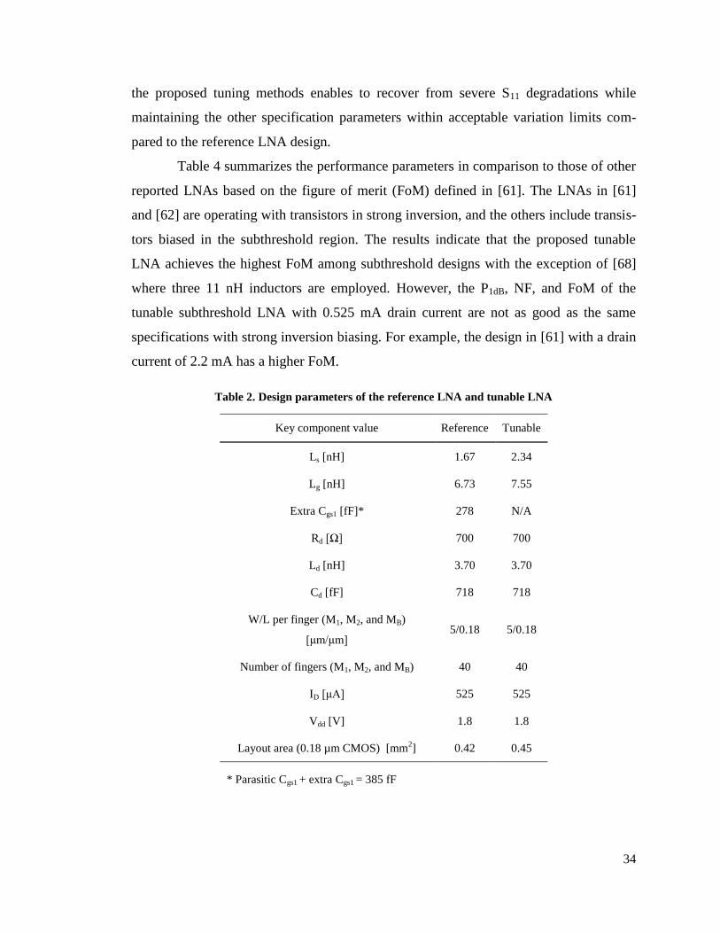
Table 2 contains the key design parameters of the reference LNA and the tunable
LNA operating at 2.4 GHz while biased in the subthreshold region. Both LNAs were
designed with the topology in Figure 10 to achieve almost identical specifications with
similar component values. An additional 278 fF MIM capacitor (extra Cgs1) was added
between the gate and source terminals of M1 in the reference LNA to obtain comparable

33
overall performance for both designs with a similar quality factor in the matching
network. In this example design, the extra capacitance degraded the simulated noise
figure by less than 0.3 dB. The tunable LNA was designed with a 5-bit binary-weighted
capacitance, where the capacitor for the smallest bit is 20 fF. Therefore, CMIM varies
from 0 fF to 620 fF as the control word (D5D4D3D2D1) is changed from [00000] to
[11111]. A fine resolution was selected in this example to demonstrate the tuning
capability of the method. Depending on the S11 requirement, a shorter control word
could be used if only coarse tuning is needed.
The layouts of both LNAs are shown in Figure 18 and Figure 19, revealing that
the occupied die area increased from 0.42 mm2 to 0.45 mm
2 to allow tuning. Post-layout
simulation results (with extracted parasitics) for the two LNAs are listed in Table 3,
which summarizes different scenarios that include specification parameters with differ-
ent device corner models, power supply variation, temperature ranges, as well as Ls and
Lg variations. Pads, bonding wires (Lbond), and QFN package parasitics (Cpack) at the
input/output pins were modeled with 120 fF, 1 nH in series with 1.2 Ω, and 60 fF,
respectively [60]. In the typical corner case with 1.8 V supply at room temperature, the
simulated specifications of the two LNAs are comparable. For brevity, Table 3 only
includes some additional cases with severe variations to demonstrate the tuning feature.
In the third simulation condition for instance, the LNA tuning improves S11 by 8.7 dB
and the linearity parameters by more than 3 dB in comparison to the reference design,
but at the expense of 0.9 dB S21 reduction with a noise figure increase of 0.9 dB due to
the slightly lower quality factor after tuning. On the contrary, in condition 5, the tuned
LNA has a 2.1 dB higher S21 with 0.9 dB noise figure improvement and slightly better
linearity. But under condition 5, the S11 parameter of the reference LNA is only -7.6 dB,
whereas S11 of the tuned LNA is -16.1 dB. If the S11 recovery requires a higher CMIM
value as for the third simulation condition in Table 3, then the tuning could cause a
slightly lower S21 and NF compared to the reference LNA due to the lower quality factor
in the input matching network. A system-level calibration scheme should take this matter
into account. Instead of tuning for optimum S11 regardless of the overall performance,
the CMIM value should be adjusted as part of the system-level calibration after it has been
determined that the specifications are not met with the default CMIM value. In summary,
34
the proposed tuning methods enables to recover from severe S11 degradations while
maintaining the other specification parameters within acceptable variation limits com-
pared to the reference LNA design.
Table 4 summarizes the performance parameters in comparison to those of other
reported LNAs based on the figure of merit (FoM) defined in [61]. The LNAs in [61]
and [62] are operating with transistors in strong inversion, and the others include transis-
tors biased in the subthreshold region. The results indicate that the proposed tunable
LNA achieves the highest FoM among subthreshold designs with the exception of [68]
where three 11 nH inductors are employed. However, the P1dB, NF, and FoM of the
tunable subthreshold LNA with 0.525 mA drain current are not as good as the same
specifications with strong inversion biasing. For example, the design in [61] with a drain
current of 2.2 mA has a higher FoM.
Table 2. Design parameters of the reference LNA and tunable LNA
Key component value Reference Tunable
Ls [nH] 1.67 2.34
Lg [nH] 6.73 7.55
Extra Cgs1 [fF]* 278 N/A
Rd [Ω] 700 700
Ld [nH] 3.70 3.70
Cd [fF] 718 718
W/L per finger (M1, M2, and MB)
[μm/μm] 5/0.18 5/0.18
Number of fingers (M1, M2, and MB) 40 40
ID [μA] 525 525
Vdd [V] 1.8 1.8
Layout area (0.18 µm CMOS) [mm2] 0.42 0.45
* Parasitic Cgs1 + extra Cgs1 = 385 fF

35
83
0μ
m
GND
Vin
Vout
VDD Itail
685μm
52
0μ
m
280μm
Figure 18. Layout of the reference LNA.
860μ
m
GND
Vin
Vout
VDDItail
690μm
530μ
m
270μm
D5
D3
D4
D1
D2
Figure 19. Layout of the tunable LNA.

36
Table 3. Post-layout simulation – comparison of the reference LNA and tunable LNA at 2.4 GHz
Reference LNA Tunable LNA
Condition 1: TT models, 27oC, Vdd
S11 [dB] -30.5 -31.8 [01010]
S21 [dB] 15.3 15.4
NF [dB] 4.4 4.6
P1dB [dBm]* -13.9 -10.7
IIP3 [dBm] -6.8 -2.3
Condition 2: FF models, 85oC, +20% Vdd
S11 [dB] -14.2 -23.5 [01111]
S21 [dB] 14.5 14.4
NF [dB] 4.2 4.7
P1dB [dBm]* -10.2 -7.5
IIP3 [dBm] -4.2 -0.7
Condition 3: FF models, 85oC, +20% Vdd,-15% Ls, -15% Lg
S11 [dB] -8.5 -17.2 [10011]
S21 [dB] 14.4 13.5
NF [dB] 4.4 5.3
P1dB [dBm]* -11.5 -5.9
IIP3 [dBm] -4.3 0.7
Condition 4: SS models, -40oC, -20% Vdd
S11 [dB] -12.9 -24.2 [00111]
S21 [dB] 13.9 15.0
NF [dB] 4.1 3.7
P1dB [dBm]* -16.3 -13.7
IIP3 [dBm] -8.8 -4.3
Condition 5: SS models, -40oC, -20% Vdd, -15% Ls, +15% Lg
S11 [dB] -7.6 -16.1 [00011]
S21 [dB] 13.3 15.4
NF [dB] 4.4 3.5
P1dB [dBm]* -16.3 -15.0
IIP3 [dBm] -8.5 -5.9
Condition 6: SS models, -40oC, -20% Vdd, -15% Ls, +15% Lg, +15% Lbond, -15% Cpack
S11 [dB] -7.2 -16.6 [00010]
S21 [dB] 13.3 15.5
NF [dB] 4.4 3.5
P1dB [dBm]* -16.2 -15.0
IIP3 [dBm] -8.2 -5.6
* Defined as the point where the gain changes by 1 dB. (Gain expansion occurs when
Pin > P1dB in this circuit, leading to increased gain but non-linear operation.)

37
Table 4. Tunable LNA performance comparison with other published results
Reference Gate length
(μm)
fc
(GHz)
S11
(dB)
Gain
(dB)
P-1dB
(dBm)
NF
(dB)
VDD/ID
(V/mA)
FoM
(MHz)
Reference LNA* 0.18
(CMOS) 2.4
-30.5 15.3 -13.9 4.4 1.8/0.525 343
Tunable LNA* -31.8 15.4 -10.7 4.6 1.8/0.525 676
[62]** N.A.
(SiGe) 5.8 -15 18.8 -14.5 2 1.8/18 95
[61]** 0.18
(CMOS) 5.7 -14 11.6 -8 3.4 1.8/2.2 730
[68]** 0.18
(CMOS) 1 -5 13.6 -0.2 4.6 1/0.26 9331
[24]** 0.13
(CMOS) 3 -14 4.5 -19.5 6.3 0.6/0.26 111
[27]** 0.18
(CMOS) 2.4 -19 21.4 -15 5.2 1.8/0.63 340
[26]** 0.18
(CMOS) 1 -25 16.8 -21 3.9 1/0.1 378
* Simulation result, ** measurement result.
3.1.3 Conclusions
A comprehensive input impedance analysis for CMOS inductor-degenerated
common-source LNAs operated in the subthreshold region has been presented. Simula-
tion results revealed that the equations permit highly accurate calculation of the required
gate and source inductance values for impedance matching under the influence of large
parasitic capacitances. In addition, an input impedance tuning method was proposed that
involves a programmable capacitance to provide digital calibration control. Simulations
of a tunable 2.4 GHz LNA design and a commensurate reference LNA were performed
with corner device models, temperature variations, supply voltage variations, and models
for off-chip bonding and package parasitics in order to evaluate the effectiveness of the
S11 tuning and to verify that it does not cause any significant performance degradation of
other specification parameters. The results showed that the tuning technique leads to 8.5
dB or more S11 improvement compared to the reference LNA design.

38
3.2 Proposed low-noise amplifier design techniques
Figure 20 shows the schematic of the proposed LNA, where inductor Lg2 and digi-
tally-programmable capacitor Cgd2_ext can improve the IIP3 in the presence of variations.
Inductor Lg1, inductor Lbuffer, and capacitor Cbuffer are off-chip components for impedance
matching purposes. Cgd2_ext is implemented with a fixed metal-insulator-metal (MIM)
capacitor (Cgd2_ext0) and a 3-bit digitally-programmable MIM capacitor (Cgd2_ext1,
Cgd2_ext2, and Cgd2_ext3) as illustrated in Figure 21. Preliminary simulations showed that
MOS capacitors can also be employed to realize Cgd2_ext, but resulting in slightly in-
creased LNA gain variation and less linearity improvement compared to metal-insulator-
metal capacitors. All passive devices (with frequency-dependent quality factor limita-
tions) and active devices were simulated using foundry-supplied models. In this section,
the bonding/package parasitics and buffer stage were neglected to simplify the small-
signal analysis. It has been shown in [64] that an inductor between the gate of the
cascode transistor and the power supply can improve stability of a common-source
cascode LNA by creating a sharp notch in the transfer function of the reverse isolation
(S12) around the operating frequency. In another related work [42], a fully differential
common-source LNA topology with an inductor at the gate of the cascode transistor and
a cross-coupling capacitor between the gate of the cascode transistor and the source of
the opposite cascode transistor was introduced to decrease the noise figure, improve the
linearity and enhance the voltage gain. Nevertheless, this LNA was biased in the strong
inversion region. The linearization method described in the next subsection was devel-
oped for subthreshold common-source cascode LNAs and does not require cross-
coupling for nonlinearity cancellation.
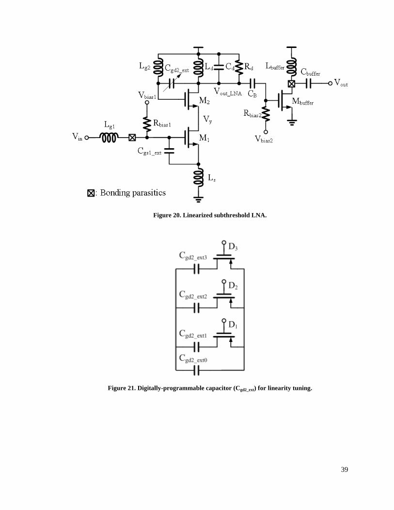
39
Figure 20. Linearized subthreshold LNA.
Figure 21. Digitally-programmable capacitor (Cgd2_ext) for linearity tuning.

40
3.2.1 Analysis and design of the linearized LNA
3.2.1.1 Linearity analysis
In this linearity analysis, the input stage (transistor M1) and cascode stage (tran-
sistor M2) of the proposed LNA in Figure 20 are split into two individual parts. Figure
22 shows the nonlinear small-signal model of the input stage where the extra metal-
insulator-metal capacitor (Cgs1_ext) is lumped into the parasitic capacitance Cgs1. The IIP3
of transistor M1 can be derived after Volterra series analysis (as in Section 2.2.1):
2,6
1
1
3
111
1,3
Ms
M
AHRIIP , (26)
where ω is the center frequency of the two intermodulation tones at ωRF1 and ωRF2, Δω is
defined as |ωRF1 - ωRF2|, and Rs is the antenna impedance of 50Ω. H1(ω) is the third-
order nonlinearity transfer function from Vin to the drain-source current (id1) of M1,
A11(ω) is the linear transfer function from the input voltage (Vx) to the gate-to-source
voltage (Vgs1), and εM1(Δω,2ω) represents the nonlinear contribution from the second-
order and third-order terms of transistor M1. Minimization of the term |ε M1 (Δω,2ω)| in
(26) leads to improved IIP3. For this reason, we will now examine the ε (Δω,2ω) term for
transistors M1 and M2. The εM1(Δω,2ω) term of M1 can be expressed as
1,1,31
2,MoBMM
gg , (27)
where
2
12
3
2
11,111,1
2
1,21,
MMMM
MMoBgggg
gg , (28)
Z
ZZCjCj
ZZCjZZCj
ggdgb
gsgd
M
111311
1111113111
1
]1[
][][1
, (29)
1312131112111
1211131112]1[
ZZZZZZCj
ZZZCjCjZZ
gd
gdgb
, (30)
111 gs
LjRZ , (31)
s
LjZ 12 , (32)

41
][][
][1
232222
2
2,1222,1
222322
2
22232
13
ZZCCgCjCjg
ZZCCCjCjZCjZ
gsgdMgdgsM
gdgsgdgsgd
, (33)
1
2222//
gbgCjLjZ , (34)
1
23////
dddCjLjRZ . (36)
The parasitic capacitance Cgb1 was included above to further improve the accura-
cy of the analysis, for which more detailed derivations are included in Appendix A. The
variables g1,M1, g2,M1 and g3,M1 are the linear gain, second-order nonlinearity coefficient
and third-order nonlinearity coefficient of transistor M1, respectively.
Figure 22. Nonlinear small-signal model of the LNA’s input stage with M1.
Figure 23 depicts the nonlinear small-signal model of the cascode stage, where
the extra metal-insulator-metal capacitor Cgd2_ext is merged with the parasitic capacitance
Cgd2. A cascode device whose gate is connected to an AC ground typically only has a
small impact on the overall linearity of a cascode common-source LNA. On the other
hand, the cascode stage with additional components at the gate of M2 in Figure 20 has a
significant impact on the overall linearity performance. The following equations give
insights into the linearity effect of the cascode device, which has not yet been clearly
analyzed in the literature for the subthreshold topology in Figure 20. Using the Volterra
series analysis method in Section 2.2.2, the amplitude at the third-order intermodulation
intercept point (AIIP3) of transistor M2 can be derived as

42
2,
1
3
4
2
3
212
2
M2IIP3,
MAH
A . (37)
The definition of ε M2(Δω,2ω) is the same as in equation (27), and can be rewritten as
2,2,32
2,MoBMM
gg , (38)
where
2
12
3
2
22,122,1
2
2,22,
MMMM
MMoBgggg
gg , (39)
23222
232222
2
2223222
232
2
]1[
1
ZZCj
ZZCC
ZZCjCjCj
ZCj
g
gd
gdgs
gdgdgs
gd
M
. (40)
The linear transfer function A21(ω) in equation (37) is derived in Appendix B. Parame-
ters g1,M2, g2,M2 and g3,M2 are the linear gain, second-order nonlinear coefficient and
third-order nonlinear coefficient of M2.
Figure 23. Nonlinear small-signal model of the LNA’s cascode stage with M2.
In addition to the nonlinearity cancellation analyzed above, a secondary mecha-
nism leads to linearity enhancement thanks to the extra components at the gate of M2.
Figure 24(a) displays the simulated voltage gain from Vin to Vy (in Figure 20). In Figure

43
24(a), the LNA with Lg2 = 3.5 nH and Cgd2_ext = 150 fF has lower voltage gain (Vy/Vin)
than the conventional cascode common-source LNAs. Hence, the attenuation due to Lg2
and Cgd2_ext contributes to linearity improvement by preventing that transistor M2 limits
the IIP3 performance. Figure 24(b) visualizes the numerical calculations of |εM2(Δω,2ω)|
versus Lg2 for three values of Cgd2_ext based on the above equations. In this design, the
cascode stage dictates the overall linearity due to the Vgs2 voltage swing boosting effect
that is evident from the equations in Appendix B. Consequently, an Lg2 value around 3.5
nH leads to optimum IIP3 in this example. While the above equations provide a theoreti-
cal foundation for the proposed linearization technique, in practice a designer can select
a reasonable Cgd2_ext value and sweep Lg2 in circuit simulations. A standard IIP3 metric
can be monitored during the simulations in lieu of the |εM2(Δω,2ω)| term. The related
reverse isolation (S12) and stability aspects for the selection of Lg2 and Cgd2_ext values are
discussed in Section 3.2.1.5.
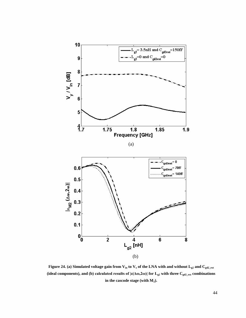
44
(a)
(b)
Figure 24. (a) Simulated voltage gain from Vin to Vx of the LNA with and without Lg2 and Cgd2_ext
(ideal components), and (b) calculated results of |ε(Δω,2ω)| for Lg2 with three Cgd2_ext combinations
in the cascode stage (with M2).

45
3.2.1.2 Voltage gain
The voltage gain of the linearized LNA can be separated to identify the contribu-
tions associated with the transistors M1 and M2. In Appendices A and B, the linear
transfer functions from Vx to V13 (in Figure 22) and from V21 to V23 (in Figure 23) are
derived, which represent the frequency-dependent voltage gains C11(ω) and C21(ω) of the
two stages. From equations (A.10) and (B.10), these voltage gains can be combined to
determine the overall LNA gain:
2111
CCAv . (41)
3.2.1.3 Input matching network
The input matching of a subthreshold common-source LNA was analyzed in [65]
without inductor Lg2. For the modified LNA (with linearization) presented in this section,
it can be shown that the input impedance under consideration of the extra components
can be estimated as
MF
inginCj
ZLjZ
1
//*
1 ; (42)
where
1
1,1
1
* 1
gs
sM
s
gs
inC
LgLj
CjZ
, (43)
11
1gbgdMF
CCAC , (44)
131,1
ZGAeffM
, (45)
1
11,1
1,1
1,1)(1
gd
gsMs
M
effMCj
CjgLj
gG
, (46)
and Z13(ω) is defined in equation (33).
3.2.1.4 Noise
The noise factor analysis for the subthreshold common-source LNA with induc-
tive source degeneration has been reported in [66] with the following result:

46
5211
51
2
1
2
2
12
222
2
t
gs
t
gs
in
D
Tso
tC
Cc
C
CQ
I
VnRCF , (47)
where Ct = Cgs1 + Cgs1_ext, ω0 is the operating frequency, γ and δ are the channel and gate
noise coefficients, α = g1,M1/gd0,M1, gd0,M1 is the channel conductance with zero drain-
source voltage, VT is the thermal voltage, Qin is the quality factor of the input matching
network, and c is the correlation parameter between the gate and channel noise currents.
3.2.1.5 Reverse isolation and stability
Compared to conventional common-source cascode LNAs, the proposed lineari-
zation method requires an inductor at the gate of the cascode transistor. As described in
[64], the reverse isolation of such an LNA can be improved in the desired frequency
band with proper sizing of the inductor at the gate of the cascode transistor. To analyti-
cally estimate the impact on reverse isolation, the transfer function from Vout_LNA to Vy in
Figure 20 can be derived from the small-signal circuit in Figure 25:
01
2
2
3
3
0
2
2
3
_
)(asasasa
bsbs
V
VsH
LNAout
y
, (48)
where
a3 = 1 + Cgb2/Cgd2,
a2 = (ro2+ZM1+gm2ro2ZM1)/(Cgs2ro2ZM1)+(ro2+ZM1)/(Cgd2ro2ZM1)+
Cgb2(1+gm2ro2+ro2/ZM1)/(Cgs2Cgd2ro2),
a1 = 1/( Cgd2Lg2),
a0 = (1+gm2ro2+ro2/ZM1)/( Cgs2Cgd2ro2Lg2),
b2 = 1/(Cgs2ro2) + 1/(Cgd2ro2)+ gm2/Cgs2 + Cgb2/(Cgs2Cgd2ro2),
b0 = 1/( Cgs2Cgd2ro2Lg2),
ro2 is the drain-source resistor of transistor M2, and ZM1 is the equivalent impedance
looking into the drain of transistor M1. Note that Lg2 and Cgd2_ext have to be chosen
properly for enhanced reverse isolation in the desired frequency band.

47
Figure 25. Simplified small-signal model for reverse isolation analysis of transistor M2.
The stability factor of the LNA is defined in [42] and [64]:
12212
22111222
SS
SSK
, (49)
where Δ = S11∙S22 – S12∙S21. The unconditional stability requirement is K > 1 and |Δ|
< 1. Note that S11 and S22 are close to zero when the input and output of the LNA are
matched to the source and load impedances. Based on the measured S-parameters (LNA
and buffer combination) presented later in this chapter, the value of |Δ| is less than 1 and
the value of K is more than 1 in the frequency range from 0.1 GHz to 8.5 GHz. The |Δ|
and K values are 0.05 and 17.67 at 1.8GHz, respectively.
From LNA simulations without buffer, the reverse isolation at 1.8 GHz with Lg2
= 3.5 nH and Cgd2_ext = 150 fF is slightly better (-29.7 dB) than without Lg2 and Cgd2_ext (-
27.4 dB). As S12 decreases, the value of K increases and |Δ| decreases, resulting in
improved stability. However, it is important to consider that the values of Lg2 and Cgd2_ext
can degrade reverse isolation and stability if they are not carefully selected. If Lg2 and
Cgd2_ext become too large, then the peak of the transfer function in equation (48) moves
from higher to lower frequency, which can cause a stability problem.
3.2.2 LNA measurement results
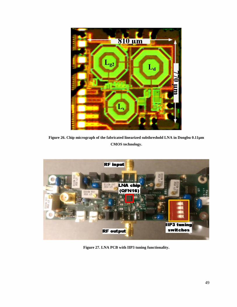
A 1.8 GHz linearized subthreshold LNA has been designed and fabricated in
Dongbu 0.11µm CMOS technology. Figure 26 displays the chip micrograph of the LNA
with an area of 810 µm × 770 µm. The Lg2 value of this design was selected to be

48
3.48nH (with a quality factor of 6.5 at 1.8 GHz), and final post-layout simulations were
performed with foundry-supplied device models for all on-chip components. As shown
in Figure 27, the prototype chip was bonded to a conventional QFN16 package that was
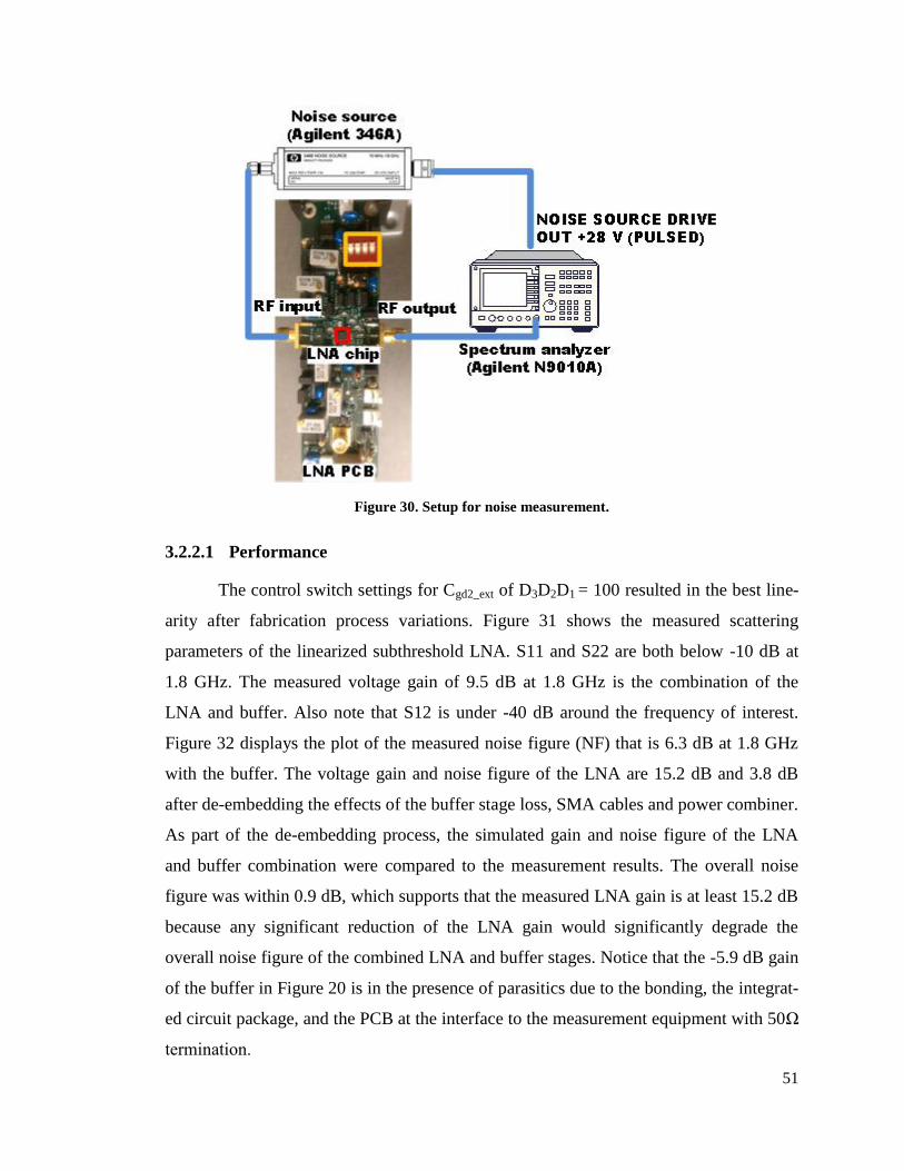
assembled on a printed circuit board (PCB) for measurements. Figures 28, 29, and 30
show the measurement setups for S-parameters, the two-tone test, and noise characteri-
zation, respectively.
Table 5 lists the key design parameters of the LNA. It consumes a 480 µA cur-
rent (with exclusion of the buffer) from a 0.7 V power supply instead of the nominal 1.2
V supply voltage for this technology. In order to limit the linearity degradation due to
the output buffer that was designed to test the LNA, a 1.2 V supply is used for the buffer.
Table 5. Linearized subthreshold LNA design parameters
Component VALUE
VDD 0.7 V
ID 480 µA
gm,M1/ID 22 S/A
Lg1 7.5 nH
Lg2 3.5 nH
Ls 2.4 nH
Cgs1_ext 130 fF
Cgd2_ext0,1,2,3 70 fF/ 20 fF/ 40 fF/ 80 fF
Ld 6.4 nH
Cd 88 fF
Rd 720 Ω
W/L per finger (M1,2) 6µm / 0.13µm
Number of fingers (M1,2) 64
49
Figure 26. Chip micrograph of the fabricated linearized subthreshold LNA in Dongbu 0.11µm
CMOS technology.
Figure 27. LNA PCB with IIP3 tuning functionality.

50
Figure 28. Setup for S-parameter measurements.
Figure 29. Two-tone test setup.
51
Figure 30. Setup for noise measurement.
3.2.2.1 Performance
The control switch settings for Cgd2_ext of D3D2D1 = 100 resulted in the best line-
arity after fabrication process variations. Figure 31 shows the measured scattering
parameters of the linearized subthreshold LNA. S11 and S22 are both below -10 dB at
1.8 GHz. The measured voltage gain of 9.5 dB at 1.8 GHz is the combination of the
LNA and buffer. Also note that S12 is under -40 dB around the frequency of interest.
Figure 32 displays the plot of the measured noise figure (NF) that is 6.3 dB at 1.8 GHz
with the buffer. The voltage gain and noise figure of the LNA are 15.2 dB and 3.8 dB
after de-embedding the effects of the buffer stage loss, SMA cables and power combiner.
As part of the de-embedding process, the simulated gain and noise figure of the LNA
and buffer combination were compared to the measurement results. The overall noise
figure was within 0.9 dB, which supports that the measured LNA gain is at least 15.2 dB
because any significant reduction of the LNA gain would significantly degrade the
overall noise figure of the combined LNA and buffer stages. Notice that the -5.9 dB gain
of the buffer in Figure 20 is in the presence of parasitics due to the bonding, the integrat-
ed circuit package, and the PCB at the interface to the measurement equipment with 50Ω
termination.

52
Figure 33 shows the measured IIP3 of the LNA and the output spectrum from a
test with a two-tone input signal (1.8 GHz and 1.7995 GHz) and an input power of -35
dBm. Figure 34 contains the plot of output power measurements from a power level
sweep of a single 1.8 GHz tone to determine the 1-dB compression point (P1dB) of the
LNA. The IIP3 and P1dB of the linearized LNA are -3.7 dBm and -12.6 dBm, respective-
ly.
Table 6 summarizes the performance of narrowband low-power RF LNAs with
operating frequencies ranging from 1 to 3 GHz in comparison to the presented design.
Most of the reported low-power LNA measurement results reveal that the IIP3 is con-
stricted to below -10 dBm except in this work as well as in [63] and [68]. The linearized
LNA fabricated with Dongbu 0.11µm CMOS technology is listed as “work 1” in Table 6.
Figure 35 shows the schematic and chip micrograph of the other linearized LNA that
was fabricated with IBM 0.13µm CMOS technology and is listed as “work 2” in Table 6.
As displayed in Figure 35(a), the LNA was designed with a source follower buffer. The
figure of merit (FOM) from [67] is used here, which is defined as 10∙log(gain × IIP3 ×
fc)/[(NF-1) × PDC]. Compared to this work with packaged chip measurements at
1.8GHz on a printed circuit board, the 1 GHz LNA in [68] was measured on a probe
station. Furthermore, the design in [68] contains a single transistor and three 11 nH
inductors. Even though the cascode stage of a subthreshold LNA has negative impact on
linearity as discussed in Section 3.2.1.1, we opted to include the cascode transistor to
maintain adequate reverse isolation (S12) in this work with linearization enhancement.
On a different note regarding Table 6, the work in [63] is a good indicator for the state-
of-the-art in low-power LNA design because this recently published fully differential
LNA was designed in 90nm CMOS technology and measured on a probe station.

53
Figure 31. Measured scattering parameters of the linearized LNA with buffer (5.9dB loss).
Figure 32. Measured noise figure of the linearized LNA with buffer.
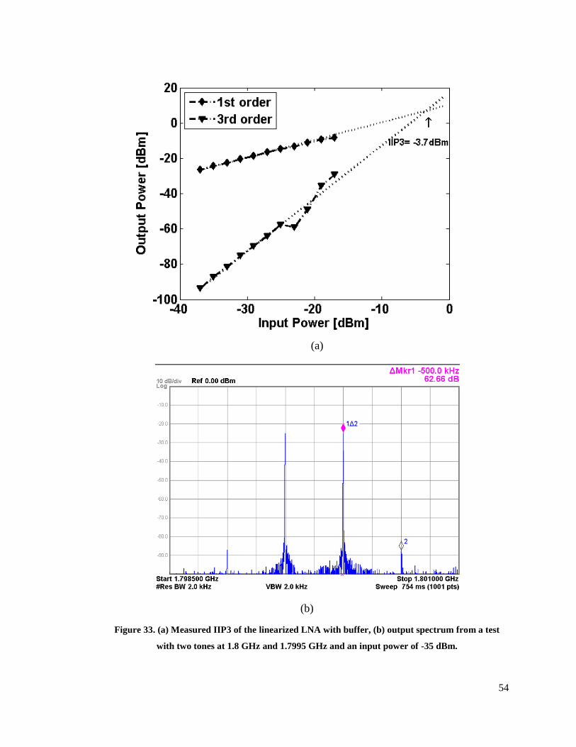
54
(a)
(b)
Figure 33. (a) Measured IIP3 of the linearized LNA with buffer, (b) output spectrum from a test
with two tones at 1.8 GHz and 1.7995 GHz and an input power of -35 dBm.

55
Figure 34. Measured 1-dB compression point of the linearized LNA with buffer at 1.8 GHz.

56
(a)
(b)
Figure 35. Linearized subthreshold LNA in IBM 0.13µm CMOS technology (a) schematic, and (b)
chip micrograph.

57
Table 6. Comparison of LNA measurement results
WORK 1* WORK 2* [23] [24] [25] [26] [63]# [68]
fc [GHz] 1.8 2.1 2.4 3 2.4 1 2.4 1
Gain [dB] 15.2 9 21.4 4.5 13.1 16.8 9.7 13.6
NF [dB] 3.8 5.8 5.2 6.3 5.3 3.9 4.36 4.6
IIP3 [dBm] -3.7 0 -11 -10.5 -12.2 -11.2 -4 7.2
P1dB [dBm] -12.6 -8.4 -15 -19.5 -19 -21 n/a -0.2
PDC [mW] 0.336 0.3 1.134 0.156 0.06 0.1 0.684 0.26
Tech. [nm] 110 130 180 130 130 180 90 180
Area [mm2] 0.624
$ 0.24
$ 0.717
$ 2
‡ 0.63
$ 0.809
‡ 0.91
$ 0.694
$
FOM [dB] 9.7 8.5 -0.7 -0.5 -6.6 5.6 3.9 17.1
* after de-embedding the effect of the buffer # fully differential structure $ without pads
‡ with pads
3.2.2.2 IIP3 tunability
The minimum and maximum capacitance values of Cgd2_ext (in Figure 21) of the
LNA in Dongbu 0.11µm CMOS technology occur with D3D2D1 = [111] and D3D2D1 =
[000], where ‘1’ and ‘0’ indicate that the switch is connected to VDD or ground, respec-
tively.
Table 7 lists the eight different capacitance combinations with the corresponding
measurement results of gain and the third-order intermodulation distortion (IM3) when
two tones at 1.8 GHz and 1.7995 GHz were applied with an input power of -35 dBm.
The results indicate that changing Cgd2_ext from 70 to 210 fF has a minor effect on the
gain while permitting to digitally tune for optimum third-order linearity performance.
Figure 36 visualizes the IIP3 vs. tuning code from simulations and measurements with
different Cgd2_ext capacitance values. In summary, the measured results demonstrate the
feasibility of the proposed technique to boost the IIP3 to achieve state-of-the-art overall
LNA performance under consideration of the key parameters in Table 6.
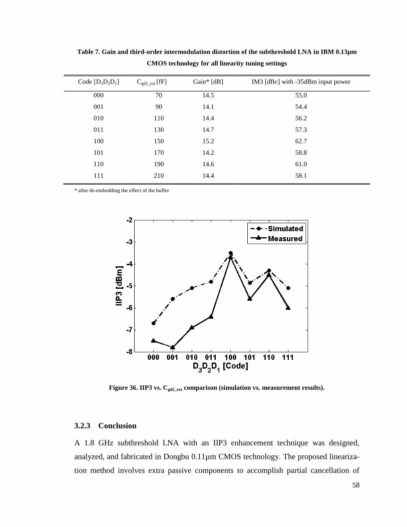
58
Table 7. Gain and third-order intermodulation distortion of the subthreshold LNA in IBM 0.13µm
CMOS technology for all linearity tuning settings
Code [D3D2D1] Cgd2_ext [fF] Gain* [dB] IM3 [dBc] with -35dBm input power
000 70 14.5 55.0
001 90 14.1 54.4
010 110 14.4 56.2
011 130 14.7 57.3
100 150 15.2 62.7
101 170 14.2 58.8
110 190 14.6 61.0
111 210 14.4 58.1
* after de-embedding the effect of the buffer
Figure 36. IIP3 vs. Cgd2_ext comparison (simulation vs. measurement results).
3.2.3 Conclusion
A 1.8 GHz subthreshold LNA with an IIP3 enhancement technique was designed,
analyzed, and fabricated in Dongbu 0.11µm CMOS technology. The proposed lineariza-
tion method involves extra passive components to accomplish partial cancellation of
59
third-order nonlinearity products. It does not require any auxiliary amplification circuitry
that would increase the power consumption. Therefore, the presented linearization
technique is well-suited for low-power applications. Measurement results of the 0.336
mW LNA on the prototype chip demonstrated an IIP3 of -3.7 dBm, a voltage gain of
15.2 dB, and a noise figure of 3.8 dB. The other 2.1 GHz subthreshold LNA with an IIP3
enhancement technique was fabricated in IBM 0.13µm CMOS technology. Measure-
ment results of the 0.3 mW LNA on the prototype chip demonstrated an IIP3 of 0 dBm,
a voltage gain of 9 dB, and a noise figure of 5.8 dB.
3.3 Proposed mixer design techniques
The third-order intermodulation intercept point (IIP3) of mixers in RF receiver
paths is a critical design specification because the mixer IIP3 is scaled down by the 10-
20 dB low-noise amplifier (LNA) gain during the calculation of the system’s input-
referred IIP3 [69]. An IIP3 below -10 dBm has been the norm for previously published
subthreshold active mixers [27] and [70], making it difficult to meet the IIP3 require-
ment for low-power wireless standards such as IEEE 802.15.4 (ZigBee) [71]. Some
linearization methods for mixers are available such as those in [72]-[73], but the main
transistors must be biased in strong inversion. Furthermore, these linearization methods
require auxiliary active circuits for IIP3 enhancement, which leads to increased power
consumption. In our previous work [74], the IIP3 of a subthreshold cascode LNA with
additional passive devices was improved by over 10 dB compared to a commensurate
LNA. Based on a similar concept, this methodology introduces an IIP3 enhancement
technique for subthreshold active mixers with extra passive components to minimize the
power consumption.
3.3.1 Analysis and design of a linearized mixer
The capacitive cross-coupling Gm-boosting technique is widely used for fully dif-
ferential common-gate LNAs (CG-LNAs) [75]-[78]. This technique can simultaneously
improve the noise and reduce the bias current for a differential CG-LNA. In [42], an
inductor connected at the gate of the cascode transistor and a cross-coupling capacitor
between the drain of the main transistor and the gate of the cascode transistor were used

60
to reduce the noise and to improve the linearity of a differential cascode common-source
LNA (CS-LNA). In [77] and [79], the capacitive cross-coupling technique has been
employed in mixers with transistors operating in strong inversion. The concept was
applied to common-gate RF stages in order to minimize noise and to improve linearity.
However, the input impedance with these design techniques is typically much lower (~
1/[2gm,RF]) than that of a mixer with a common-source input stage. For instance, in case
an LNA with a high output impedance is connected to a linearized common-gate mixer,
then a power-consuming buffer stage should be inserted to drive the mixer.
Figure 37 shows the schematic of the proposed mixer [80], where inductor L1,
inductor L2, and capacitor Cc enable IIP3 improvement. The transconductance stages
(M1, M2) and switches (M3, M4, M5, M6) are biased in subthreshold, which increases the
voltage headroom as a result of the low drain-source voltage overdrive requirement.
Transistors M3 and M6 are driven by LO+ while M4 and M5 are driven by LO-, where
LO+ and LO- are anti-phase signals. Figure 38 shows the small-signal model of the
mixer under the assumption that the signals at LO+/LO- are large enough to model M3-
M6 as switches. Based on simulations, it is desirable to operate M3-M6 in deep sub-
threshold to improve the transconductances (gm3 - gm6) of these switching transistors.
The parasitic capacitances at their sources are taken into account in the small-signal
model. The drain-to-source resistances (rds3 - rds6) of M3-M6 are neglected in this analysis
because they are much larger than Zload = Rout//(jωRFCout )-1
. Since the small-signal model
in Figure 38 is a fully symmetric circuit, it can be simplified further with the equivalent
half-circuit shown in Figure 39(a). The current summation equations for nodes 1 and 2 in
Figure 39(a) are
)()2
(
3
111 sdcRF
M
d
gsmd
RF
gdRFvvCj
Z
vvgv
vCj , (50)
)()(
1
111 sdcRF
RF
s
gsgsRFmvvCj
Lj
vvCjg
, (51)
where )(
1)(
433
23
gsgsRFm
RFRFMCCjg
LjjZ
, gm1 is the transconductance of
M1, Cgd1 and Cgs1 are the parasitic gate-to-drain and gate-to-source capacitances of M1
respectively, and gm3 = gm4 = gm5 = gm6. Note that ZM3 is independent of Zload in this
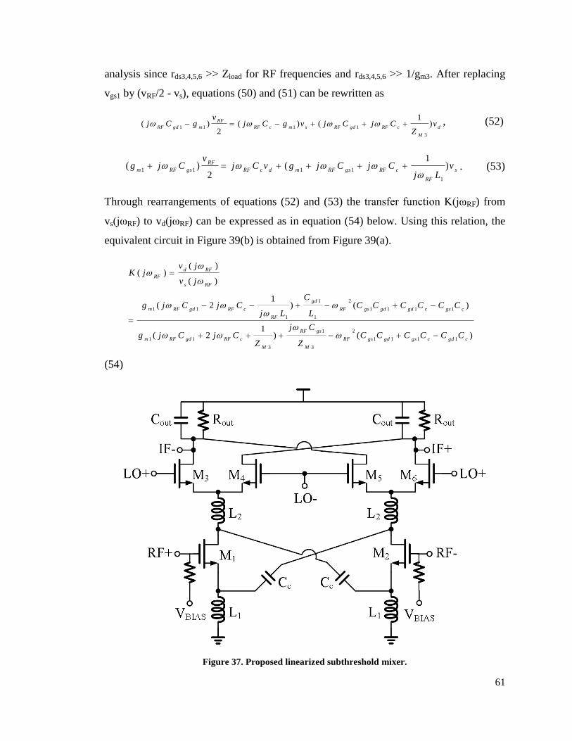
61
analysis since rds3,4,5,6 >> Zload for RF frequencies and rds3,4,5,6 >> 1/gm3. After replacing
vgs1 by (vRF/2 - vs), equations (50) and (51) can be rewritten as
d
M
cRFgdRFsmcRF
RF
mgdRFv
ZCjCjvgCj
vgCj )
1()(
2)(
3
1111 , (52)
s
RF
cRFgsRFmdcRF
RF
gsRFmv
LjCjCjgvCj
vCjg )
1(
2)(
1
1111
. (53)
Through rearrangements of equations (52) and (53) the transfer function K(jωRF) from
vs(jωRF) to vd(jωRF) can be expressed as in equation (54) below. Using this relation, the
equivalent circuit in Figure 39(b) is obtained from Figure 39(a).
)()1
2(
)()1
2(
)(
)()(
1111
2
3
1
3
11
1111
2
1
1
1
11
cgdcgsgdgsRF
M
gsRF
M
cRFgdRFm
cgscgdgdgsRF
gd
RF
cRFgdRFm
RFs
RFd
RF
CCCCCCZ
Cj
ZCjCjg
CCCCCCL
C
LjCjCjg
jv
jvjK
(54)
Figure 37. Proposed linearized subthreshold mixer.

62
Figure 38. Small-signal model of the linearized mixer.
(a) (b)
Figure 39. (a) Equivalent half-circuit of the small-signal model in Figure 38,
(b) simplified small-signal model.
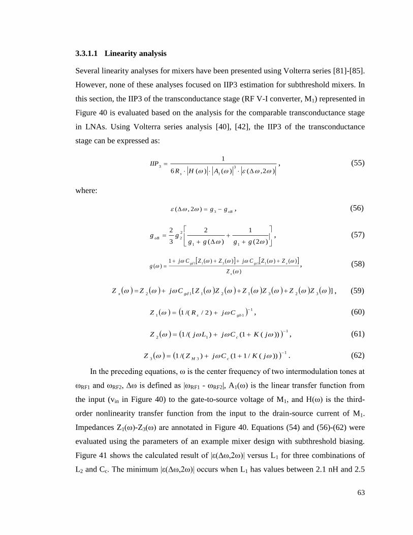
63
3.3.1.1 Linearity analysis
Several linearity analyses for mixers have been presented using Volterra series [81]-[85].
However, none of these analyses focused on IIP3 estimation for subthreshold mixers. In
this section, the IIP3 of the transconductance stage (RF V-I converter, M1) represented in
Figure 40 is evaluated based on the analysis for the comparable transconductance stage
in LNAs. Using Volterra series analysis [40], [42], the IIP3 of the transconductance
stage can be expressed as:
)2,()()(6
1
3
1
3
AHRIIP
s
, (55)
where:
oB
gg 3
)2,( , (56)
)2(
1
)(
2
3
2
11
2
2 gggg
ggoB
, (57)
)(
)()()()(1)(
11311
x
xgsgd
Z
ZZCjZZCjg
, (58)
][32312112 ZZZZZZCjZZ
gdx , (59)
1
11)2//(1
gbsCjRZ , (60)
1
12))(1()/(1
jKCjLjZ
c, (61)
1
33))(/11()/(1
jKCjZZ
cM. (62)
In the preceding equations, ω is the center frequency of two intermodulation tones at
ωRF1 and ωRF2, Δω is defined as |ωRF1 - ωRF2|, A1(ω) is the linear transfer function from
the input (vin in Figure 40) to the gate-to-source voltage of M1, and H(ω) is the third-
order nonlinearity transfer function from the input to the drain-source current of M1.
Impedances Z1(ω)-Z3(ω) are annotated in Figure 40. Equations (54) and (56)-(62) were
evaluated using the parameters of an example mixer design with subthreshold biasing.
Figure 41 shows the calculated result of |ε(Δω,2ω)| versus L1 for three combinations of
L2 and Cc. The minimum |ε(Δω,2ω)| occurs when L1 has values between 2.1 nH and 2.5

64
nH in this example, indicating that the IIP3 can be improved by the proper selection of
L1, L2, and Cc. Moreover, Figure 41 reveals that there are multiple solutions to minimize
|ε(Δω,2ω)|, which relate to the following design tradeoffs: a higher L2 value typically
results in a lower quality factor and larger layout area, and a high Cc value could reduce
the conversion gain as discussed in the next section.
Figure 40. Nonlinear small-signal model of the mixer’s transconductance stage.
Figure 41. Example evaluation: |ε(Δω,2 ω)| vs. L1 for different values of Cc.
0 1 2 3 4 5 60
0.1
0.2
0.3
0.4
0.5
L1 [nH]
| (
, 2
)|
L2 = 3.5nH & C
c= 260fF
L2 = 5.5nH & C
c= 230fF
L2 = 7.5nH & C
c= 160fF

65
3.3.1.2 Conversion gain
Figure 42 displays the equivalent circuit of the proposed mixer, in which M1 pro-
duces a current equal to gm1∙vgs1. Using equations (53) and (54), the relationship between
the input voltage vRF/2 and vd can be expressed as voltage gain α1, which can be divided
by ZM3 to obtain the corresponding current flowing through L2. The small-signal current
(Iout1) can be expressed by taking into account that the current through L2 splits accord-
ing to the impedances of Cgs3+Cgs4 and 1/gm3, which is captured by factor α2:
tv
ZtI
RF
RF
M
out
cos
23
21
1
, (63)
where:
)(
)1
(
1
11
11
1
RF
RF
cRFgsRFm
cRF
gsRFm
jK
LjCjCjg
Cj
Cjg
, (64)
)(
433
3
2
gsgsRFm
m
CCjg
g
. (65)
From equation (63), the voltage conversion gain can be derived by modeling the
operation with a multiplication of Iout1 by a square waveform [69]:
D
M
MixerZ
ZCG
3
212
, (66)
where ZD = Rout//(jωIFCout )-1
is equal to Zload evaluated at ωIF.
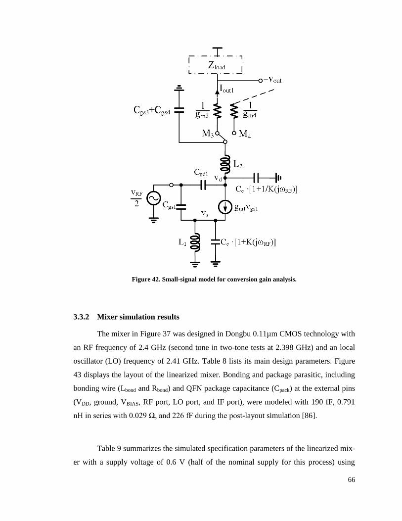
66
Figure 42. Small-signal model for conversion gain analysis.
3.3.2 Mixer simulation results
The mixer in Figure 37 was designed in Dongbu 0.11µm CMOS technology with
an RF frequency of 2.4 GHz (second tone in two-tone tests at 2.398 GHz) and an local
oscillator (LO) frequency of 2.41 GHz. Table 8 lists its main design parameters. Figure
43 displays the layout of the linearized mixer. Bonding and package parasitic, including
bonding wire (Lbond and Rbond) and QFN package capacitance (Cpack) at the external pins
(VDD, ground, VBIAS, RF port, LO port, and IF port), were modeled with 190 fF, 0.791
nH in series with 0.029 Ω, and 226 fF during the post-layout simulation [86].
Table 9 summarizes the simulated specification parameters of the linearized mix-
er with a supply voltage of 0.6 V (half of the nominal supply for this process) using

67
device models for three different process corners in Cadence Spectre. This linearization
technique enables to achieve an IIP3 of -0.02 to 6.7 dBm and a 1dB compression point
(P1dB) of -14.6 to -9.6 dBm with low power consumption ranging from 309 to 515 µW
depending on the process corner case. In the fast and slow corner cases, the |ε(Δω,2ω)|
term is no longer optimal due to the changes of the contribution and distribution of the
parasitics at the transconductance and switching stages. The gain variation in the corner
cases also impacts the IIP3 according to equation (55). Figure 44 displays output spec-
trum from a transient simulation with an input power level of -30 dBm, at which the
intermodulation distortion tones are approximately 73 dB below the two test tones.
Figure 45 shows the IIP3 plot for the linearized mixer, which demonstrates the capability
of the third-order nonlinearity cancellation for input power levels up to -25 dBm.
The proposed mixer can achieve the best IIP3 and moderate voltage gain by se-
lecting the appropriate power level at the LO port. Figure 46 shows the IIP3 and voltage
gain versus power level at the LO port. Under the best IIP3 condition, the switches (M3,
M4, M5, and M6) are biased in deep subthreshold as mentioned in Chapter 2. Compared
to designs with strong inversion biasing, the LO signal swing required for switching is
smaller because the subthreshold transistors have a reduced gate-source overdrive
voltage, which translates into more power savings in the LO signal generation and buffer
circuitry. The RF and switching stages are operated in subthreshold, and a large LO
signal swing causes the drain-source voltage (vDS) of the RF input transistors (M1 and
M2) to be large. Hence, the total current from transistors M1 and M2 will be modulated
due to the vDS voltage swing in combination with short-channel effects. Furthermore, the
resulting gm/ID variations also change the instantaneous operating points of transistors
M1 and M2. As a consequence, the mixer will not operate at its optimal IIP3 point. Table
10 summarizes the performance parameters in comparison to those of other reported
low-power mixers. Although the mixers in [87] and [88] are operating with transistors in
strong inversion, their power consumptions are low compared to conventional designs.
The double-sideband noise figures reported in [70] and [27] were converted to single-
sideband equivalents for the comparison in Table 10. In summary, the results indicate
that the proposed linearization technique achieves the highest IIP3 and the lowest power
with acceptable gain and noise figure compared to the references. The 0.745 mm2 layout

68
area of the proposed mixer is relatively large compared to the references due to the extra
inductors. However, the layout in Figure 43 has a similar size as other high-performance
mixers that use inductors for performance enhancements, such as the 1 mm2 mixer in
[87] and the 1.2 mm2 mixer in [89].
Table 8. Mixer design parameters
Key Component Value
VDD [V] 0.6
L1 [nH] 2.47
L2 [nH] 5.45
Cc [fF] 340
Rout [Ω] 825
Cout [pF] 1.28
W/L per finger (M1,2) [μm/μm] 6/0.13
Number of fingers (M1,2) 64
W/L per finger (M3,4,5,6) [μm/μm] 5.8/0.13
Number of fingers (M3,4,5,6) 64
860 µm
866 µ
m
L1 L1
L2L2
Figure 43. Layout of the linearized mixer.

69
Table 9. Simulation results with fRF1 = 2.4 GHz, fRF2 = 2.398 GHz, and fLO = 2.41 GHz for process
corner cases (VDD = 0.6V)
Corner Case SS TT FF
Gain [dB] 7.6 8.6 8.8
NFSSB [dB] 21.1 19.2 17.8
P1dB [dBm] -9.6 -13.2 -14.6
IIP3 [dBm] 5.2 6.7 -0.02
ID [µA] 514.6 705.5 858.1
PDC [µW] 309 423 515
Figure 44. Output spectrum from a simulation with -30 dBm input power.
Figure 45. IIP3 curve (typical corner case in Table 9).
-50 -40 -30 -20 -10 0 10-150
-100
-50
0
Input Power [dBm]
Ou
tpu
t P
ow
er
[dB
m]
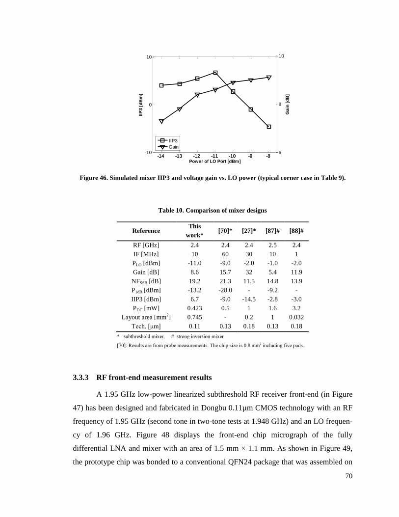
70
Figure 46. Simulated mixer IIP3 and voltage gain vs. LO power (typical corner case in Table 9).
Table 10. Comparison of mixer designs
Reference This
work* [70]* [27]* [87]# [88]#
RF [GHz] 2.4 2.4 2.4 2.5 2.4
IF [MHz] 10 60 30 10 1
PLO [dBm] -11.0 -9.0 -2.0 -1.0 -2.0
Gain [dB] 8.6 15.7 32 5.4 11.9
NFSSB [dB] 19.2 21.3 11.5 14.8 13.9
P1dB [dBm] -13.2 -28.0 - -9.2 -
IIP3 [dBm] 6.7 -9.0 -14.5 -2.8 -3.0
PDC [mW] 0.423 0.5 1 1.6 3.2
Layout area [mm2] 0.745 - 0.2 1 0.032
Tech. [μm] 0.11 0.13 0.18 0.13 0.18
* subthreshold mixer, # strong inversion mixer
[70]: Results are from probe measurements. The chip size is 0.8 mm2 including five pads.
3.3.3 RF front-end measurement results
A 1.95 GHz low-power linearized subthreshold RF receiver front-end (in Figure
47) has been designed and fabricated in Dongbu 0.11µm CMOS technology with an RF
frequency of 1.95 GHz (second tone in two-tone tests at 1.948 GHz) and an LO frequen-
cy of 1.96 GHz. Figure 48 displays the front-end chip micrograph of the fully
differential LNA and mixer with an area of 1.5 mm × 1.1 mm. As shown in Figure 49,
the prototype chip was bonded to a conventional QFN24 package that was assembled on
-14 -13 -12 -11 -10 -9 -8-10
0
10
IIP
3 [
dB
m]
Power of LO Port [dBm]-14 -13 -12 -11 -10 -9 -8
6
8
10
Gain
[d
B]
IIP3
Gain

71
a printed circuit board (PCB) for measurements. Figure 50 visualizes the test setup of
the RF front-end. Table 11 lists the key design parameters of the LNA and mixer. The
front-end consumes a 1500 µA current from a 0.6 V power supply instead of the nominal
1.2 V supply voltage in 0.11µm CMOS technology.
Figure 47. Schematic of the linearized subthreshold RF front-end.
Figure 48. Chip micrograph of the fabricated linearized subthreshold RF front-end in Dongbu
0.11µm CMOS technology.

72
Figure 49. PCB for RF front-end testing.
Figure 50. Block diagram of the RF front-end measurement setup.

73
Table 11. RF front-end design parameters
Component VALUE
LNA circuit
VDD 0.6 V
ID 875 µA
Lg1 6.2 nH
Lg2 3.5 nH
Ls 2.4 nH
Cgs1_ext 130 fF
Cgd2_ext 150 fF
Ld 6.4 nH
Cd 88 fF
Rd 720 Ω
W/L per finger (M1,2,3,4) 6µm / 0.13µm
Number of fingers (M1,2,3,4) 64
Mixer circuit
VDD 0.6 V
ID 625 µA
L1 2.7 nH
L2 5.8 nH
Cc 337 fF
Cout 1178 fF
Rd 1 KΩ
W/L per finger (M5,6) 6µm / 0.13µm
Number of fingers (M5,6) 64
W/L per finger (M7,8,9,10) 5.8µm / 0.13µm
Number of fingers (M7,8,9,10) 64
Figure 51 shows the measured S11 of the linearized subthreshold RF front-end.
S11 is below -10 dB at 1.95 GHz. Figure 52 displays the plot of the measured double-
side band noise figure (NFDSB) that is 14 dB at 10 MHz with the input balun. After de-
embedding the effect of the input balun loss (5.5 dB), the single side band noise figure of
the RF front-end is 9.5 dB at 10 MHz. Figure 53 shows the measured IIP3 of the front-
end and the output spectrum from a test with a two-tone input signal and an input power
of -36.5 dBm. Figure 54 contains the plot of output power measurements from a power
level sweep of a single 10 MHz tone to determine the 1-dB compression point (P1dB) of
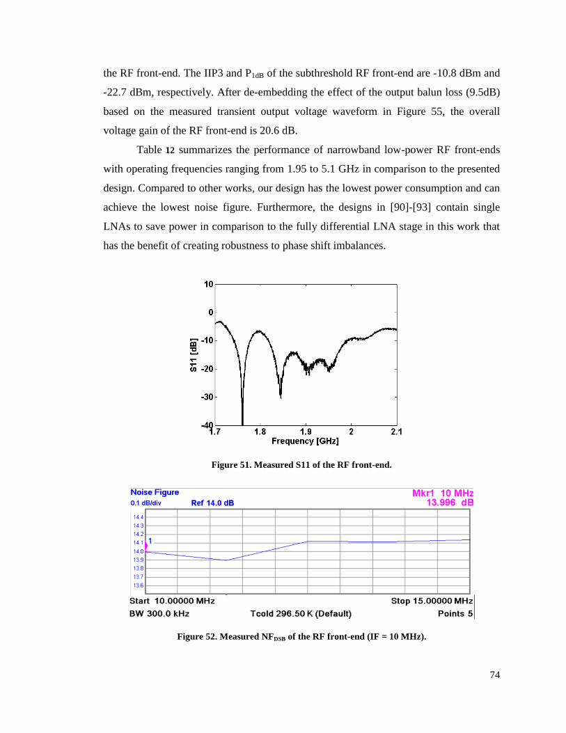
74
the RF front-end. The IIP3 and P1dB of the subthreshold RF front-end are -10.8 dBm and
-22.7 dBm, respectively. After de-embedding the effect of the output balun loss (9.5dB)
based on the measured transient output voltage waveform in Figure 55, the overall
voltage gain of the RF front-end is 20.6 dB.
Table 12 summarizes the performance of narrowband low-power RF front-ends
with operating frequencies ranging from 1.95 to 5.1 GHz in comparison to the presented
design. Compared to other works, our design has the lowest power consumption and can
achieve the lowest noise figure. Furthermore, the designs in [90]-[93] contain single
LNAs to save power in comparison to the fully differential LNA stage in this work that
has the benefit of creating robustness to phase shift imbalances.
Figure 51. Measured S11 of the RF front-end.
Figure 52. Measured NFDSB of the RF front-end (IF = 10 MHz).

75
(a)
(b)
Figure 53. (a) Measured IIP3 of the RF front-end with balun (9.5dB loss), (b) output spectrum from
a test with two tones at 10 MHz and 12 MHz and an input power of -36.5 dBm.

76
Figure 54. Measured 1-dB compression point of the RF front-end with input and output baluns (at
IF = 10 MHz).
Figure 55. Measured output amplitude before the output balun.

77
Table 12. Comparison of low-power RF front-ends
THIS WORK [90] *# [91]
# [92]
# [93]
fRF [GHz] 1.95 5.1 2.4 2.445 2.6
fIF [MHz] 10 10 2 10 n/a
PLO [dBm] -9 -5 n/a n/a n/a
S11 [dB] -20 n/a -17 n/a -20.6
Gain [dB] 20.6 27 20.5 30 12.5
NFBSB [dB] 6 16 10.2 7.5 n/a
IIP3 [dBm] -10.8 -3 -7.8 -16.2 -4.04
P1dB [dBm] -22.7 n/a -20 -26 -9
PDC [mW] 0.9 1 1.08 4.68 2.724
Tech. [nm] 110 180 180 90 180
Area [mm2] 1.65
$ 0.856
‡ 1.69
‡ 0.74
$ 1.44
$
* passive mixer # single LNA
$ without pads
‡ with pads
3.3.4 Conclusion
A 2.4 GHz mixer was designed in Dongbu 0.11µm CMOS technology to demon-
strate a proposed IIP3 enhancement technique for subthreshold mixers. Post-layout
simulations resulted in an IIP3 of 6.7 dBm, a voltage gain of 8.6 dB, and a single-
sideband noise figure of 19.2 dB with a power consumption of 0.423 mW. The lineariza-
tion method mixer does not require an auxiliary amplifier to boost the mixer linearity,
making it suitable for low-power narrow-band wireless standards. For further validation
of the new design technique, a 1.95 GHz RF receiver front-end including an LNA and a
mixer was fabricated in Dongbu 0.11µm CMOS technology. Measurements resulted in
an IIP3 of -10.8 dBm, a voltage gain of 20.6 dB, and a single-sideband noise figure of
11.5 dB with a power consumption of 0.9 mW.

78
4. Analog Frond-End Circuits for Brain Signal Acquisitions with Dry
Electrodes
A possible solution for boosting input impedance would be to add a classical
negative impedance converter (NIC) at the input of an instrumentation amplifier (IA).
Figure 56 shows a simplified NIC circuit that could be used to generate a negative
capacitance at the input node of the IA if the component Z is a capacitor [94]. However,
this approach would require an additional amplifier, whose power and area consumption
is undesirable. Furthermore, the additional noise from the operational amplifier at the
input of the IA would have to be carefully assessed.
Figure 56. Basic negative impedance converter (NIC), where Zin = -Z when R1 = R2.
4.1 System-level considerations
The negative capacitance generation scheme proposed in this chapter is integrat-
ed into the IA and thereby avoids an extra amplifier. The discussed IA was designed as
part of a larger research project in which the goal is to automate the input capacitance
cancellation as visualized in Figure 57 with on-chip monitoring using a digital signal
processor (DSP) and with a programmable capacitor bank within the IA for tuning [95]-
[96]. The calibration system will include an on-chip test current generator (itest) with high
output impedance and low output noise. As shown in Figure 58, the test current genera-
tor consists of a relaxation oscillator, a limiter, a frequency divider, and an operational
transconductance amplifier (OTA) [97]-[98]. The on-chip oscillator generates a 20 KHz
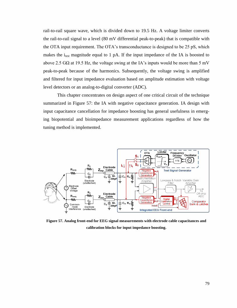
79
rail-to-rail square wave, which is divided down to 19.5 Hz. A voltage limiter converts
the rail-to-rail signal to a level (80 mV differential peak-to-peak) that is compatible with
the OTA input requirement. The OTA’s transconductance is designed to be 25 pS, which
makes the itest magnitude equal to 1 pA. If the input impedance of the IA is boosted to
above 2.5 GΩ at 19.5 Hz, the voltage swing at the IA’s inputs would be more than 5 mV
peak-to-peak because of the harmonics. Subsequently, the voltage swing is amplified
and filtered for input impedance evaluation based on amplitude estimation with voltage
level detectors or an analog-to-digital converter (ADC).
This chapter concentrates on design aspect of one critical circuit of the technique
summarized in Figure 57: the IA with negative capacitance generation. IA design with
input capacitance cancellation for impedance boosting has general usefulness in emerg-
ing biopotential and bioimpedance measurement applications regardless of how the
tuning method is implemented.
Figure 57. Analog front-end for EEG signal measurements with electrode cable capacitances and
calibration blocks for input impedance boosting.

80
Oscillator
gm
FrequencyDivider
OTA
N
itest itest
Limiter
Vin
Vout
Instrumentation Amplifier
Zin 2|itestZinAIA|~
Figure 58. Current injection with the test current generator.
4.2 Instrumentation amplifier
Figure 59(a) shows the schematic of the widely used IA topology with direct cur-
rent feedback, where the DC gain of the IA is decided by the ratio R2/R1, and the
dominant pole depends on R2 and C2 [95], [99], [100]. For the input impedance test of
the IA, the resistor R2 has been designed with digital programmability to implement four
different gain modes as illustrated in Figure 59(b), where the smallest gain setting is
20dB. The amplifier B1 was realized as in [99]. Figure 59(c) shows the input biasing
circuity of the IA using pseudo resistors [101]. The effective impedances from the inputs
(vi+, vi-) of the IA to Vbias are 4.7 GΩ at DC and 3.36 GΩ at 100Hz, respectively. The
transfer functions from the inputs (vi+, vi-) to vA, vB, vC, vD, vE, vF, vH, vI, vJ, vK, and vo are
analyzed in Section 4.2.1 to evaluate the possibilities for negative capacitance generation
feedback (NCGFB). Since nodes vC and vD in Figure 59(a) are the most appropriate
locations to obtain suitable gains for generating negative capacitances at the inputs (vi+,
vi-), the NCGFB realization at these two nodes is elaborated in Section 4.2.2.

81
(a)
(b)
(c)
Figure 59. (a) Instrumentation amplifier (IA) with direct current feedback and negative capacitance
generation feedback (NCGFB); (b) variable R2 implementation; (c) input biasing circuitry.

82
4.2.1 Instrumentation amplifier small-signal model analysis
Figure 60(a) shows the small-signal model of the IA’s input stage and the current
feedback loop for solving the transfer functions from the inputs to internal nodes. All
parasitic capacitances are omitted during the analysis because the typical applications of
this IA are at low frequencies (below 1 KHz). It is also noteworthy that the small-signal
inputs (vA and vB) of the differential pair (M5 and M6) in the feedback loop are not truly
differential due to the asymmetric characteristics looking into vA (M3 is diode-connected)
and vB (M4 is not diode-connected). Hence, the phase of vB follows that of vA, and vG is
not a virtual ground. For this reason, the small-signal drain-source resistance (1/gds,Mtail)
of Mtail should be taken into account during the analysis. Without the effect of the
NCGFB, the current summation equations at nodes 1 through 4 in Figure 60(a) are:
0)(9,1,
1
DMmiEMm
FEvgvvg
R
vv, (67)
0)(10,2,
1
CMmiFMm
FEvgvvg
R
vv, (68)
0)(
4,2,
AMmiFMmvgvvg , (69)
0)(6,5,,6,6,5,5,
BMmAMmGMtaildsMmbMmMmbMm
vgvgvggggg ; (70)
where gm,M1-gm,M10 are the transconductances of M1-M10, gmb,M5 and gmb,M6 are the body
effect transconductances of M5 and M6, and gds,Mtail is the small-signal drain-source
admittance of Mtail. From Figure 60(a), the voltages vA, vC, vD, vG can be expressed as
3,
1,)(
Mm
iEMm
Ag
vvgv
, (71)
7,
5,5,5,)(
Mm
AMmGMmbMm
Cg
vgvggv
, (72)
8,
6,6,6,)(
Mm
BMmGMmbMm
Dg
vgvggv
, (73)
)(
3,3,
3,5,
MmbMm
AMmCMm
Ggg
vgvgv
. (74)
Note that the conditions gm1 = gm2, gm3 = gm4, gm5 = gm6, gm7 = gm8, gm9 = gm10, and gmb5 =
gmb6 are valid for this analysis in the absence of device mismatches. Furthermore, the

83
same definitions as in [95] are used next: vin = vi+ - vi- = vE - vF, where vi+ = vin/2 and vi- =
-vin/2. With these definitions, the following voltage gains from vin to vA-G can be derived
from the above equations:
D
gg
v
vA
MtaildsMm
in
A
AV
,7,
,
, (75)
D
gg
Rgg
g
v
vA
MtaildsMm
MmMm
Mm
in
B
BV
,7,
19,5,
7,
,
2
, (76)
Dg
ggg
Rgv
vA
Mm
MtaildsMmMm
Mmin
C
CV
9,
,7,3,
19,
,
1, (77)
Dg
ggg
Rgv
vA
Mm
MtaildsMmMm
Mmin
D
DV
9,
,7,3,
19,
,
1, (78)
Dg
ggg
v
vA
Mm
MtaildsMmMm
in
E
EV
1,
,7,3,
,2
1, (79)
Dg
ggg
v
vA
Mm
MtaildsMmMm
in
F
FV
1,
,7,3,
,2
1, (80)
Dg
gg
v
vA
Mm
MmMm
in
G
GV
9,
2
7,3,
,
2; (81)
where: D=[(2∙gm,M5+2∙gmb,M5+gds,Mtail)∙gm,M3∙gm,M7-gm,M5∙gm,M9∙gds,Mtail]∙R1.
For the output stage of the IA, the current summation equations at nodes 5 and 6 in
Figure 60(b) are:
0)()(
11,13,
2
CMmoIMm
HIVgvvg
Z
vv, (82)
0)(
12,14,
2
DMmHMm
HI vgvgZ
vv ; (83)
where Z2 = R2||(1/sC2). Note that the design conditions gm11 = gm12, gm13 = gm14, and gm15
= gm16 are assumed for this analysis in the absence of device mismatches. From Figure
60(b), the voltages vK, vJ, and vo can be expressed as
84
15,
13,)(
Mm
oIMm
Kg
vvgv
, (84)
16,
14,
Mm
HMm
Jg
vgv , (85)
)(1, KJBVo
vvAv . (86)
Based on (84), (85) and (86), if the voltage gain (AV,B1) of B1 is approximated to be
infinite for simplicity, vo can be rewritten as
HIo
vvv . (87)
Note that gm9 = gm11 is another condition used in this design. The voltage gains from vin
to vH-K and to vo can be derived from the above equations and conditions:
Dg
ggg
Rgv
vA
Mm
MtaildsMmMm
Mmin
H
HV
13,
,7,3,
113,
,
2, (88)
Dg
ggg
RgR
Z
v
vA
Mm
MtaildsMmMm
Mmin
I
IV
13,
,7,3,
113,1
2
,
2, (89)
Dg
ggg
Rgg
g
v
vA
Mm
MtaildsMmMm
MmMm
Mm
in
J
JV
13,
,7,3,
113,15,
13,
,
2, (90)
Dg
ggg
Rgg
g
v
vA
Mm
MtaildsMmMm
MmMm
Mm
in
K
KV
13,
,7,3,
113,15,
13,
,
2, (91)
1
2
19,
211,
,R
Z
Rg
Zg
v
vA
Mm
Mm
in
o
oV
. (92)
From (75) and (76) it can be observed that AV,B is always larger than AV,A, and
that AV,A and AV,B have the same phase. Equations (77) and (78) show that AV,C and AV,D
are in anti-phase. Although these gain magnitudes are not equal, nodes vC and vD are
well-suited as points at which the NCGFB can be added. From (79) and (80), the gains
AV,E and AV,F have the same phase if gm,M3∙gm,M7∙gds,Mtail/(gm,M1∙D) > 0.5, which would
complicate the use of nodes vE and vF for the NCGFB. The gains AV,H, AV,I, AV,J and AV,K

85
in the output stage of the IA have the same phase. Thus, these nodes are not suitable for
adding the proposed NCGFB.
(a)
(b)
Figure 60. (a) Small-signal model of the IA’s input and feedback stages; (b) small-signal model of
the IA’s output stage.

86
4.2.2 Negative capacitance generation feedback analysis
Figure 61 shows the proposed NCGFB implementation with an 8-bit digitally-controlled
capacitor (Cp - 27∙Cp) and one fixed capacitor (Cp0) between nodes vi+ and vC. The
maximum and minimum capacitance values occur with Sp7,6,5,4,3,2,1,0 = [11111111] and
[00000000] respectively, where '1' or '0' indicate that the switch is turned “on” or “off”.
The same programmable capacitor configuration was connected between nodes vi- and
vD with control switches Sn7,6,5,4,3,2,1,0. Neglecting the very high resistance at the gates of
the transistors, the input impedances (Zinp and Zinn) in Figure 57 can be derived as
itotalsp
inpsCsC
sZ
,
1)( , (93)
itotalsn
innsCsC
sZ
,
1)( ; (94)
where Csp and Csn are the lumped cable and PCB capacitances at the positive and nega-
tive inputs of the IA, and Ctotal,i+ and Ctotal,i- represent the IA’s total equivalent
capacitances at the inputs vi+ and vi- respectively. The tuning range of the 8-bit capaci-
tors can be designed to compensate for the 50-200 pF capacitances from the cables and
PCB by generating negative Ctotal,i+ and Ctotal,i- values through the presented NCGFB
configuration. This property becomes evident after using Miller approximations to
express Ctotal,i+ and Ctotal,i- in terms of previously derived gains:
)21(])2([
)21()21(
,
7
0
0
,1,,1,,
CV
i
pi
i
pp
AVMgdEVMgsitotal
ASCC
ACACC
, (95)
)21(])2([
)21()21(
,
7
0
0
,2,,2,,
DV
i
ni
i
nn
BVMgdFVMgsitotal
ASCC
ACACC
; (96)
where Cgs,X and Cgd,X are the parasitic gate-source and gate-drain capacitances of transis-
tor MX. The simulation result in Figure 62 reveals that the input impedance is greatly
boosted by the NCGFB activation, and that the voltage swing at the IA input is far above
the noise level during the test current injection with the OTA.

87
Figure 61. Negative capacitance generation feedback (NCGFB) with programmable capacitors
between nodes vi+ and vC (and nodes vi- and vD).
3
4
1
5
Vo
lta
ge
Sw
ing
in
to IA
(m
V)
-2
-1
0
-5
-4
-3
2
Time (s)1.7 1.8 1.9 2.0
Cp=50pF w/o NCGFB Cp=50pF w NCGFB
Figure 62. Voltage swings at the IA input with current injection from the OTA for two cases: i.) with
NCGFB, ii.) without NCGFB. (Noise was activated during the transient simulations based on the
integrated noise density from 0.01Hz to 100Hz.)
4.3 IA simulation results
The IA in Figure 59 was designed in IBM 0.13μm CMOS technology for EEG
signal measurement applications. A commensurate IA without NCGFB was designed as
reference for comparison. Table 13 contains the key design parameters of both IAs.
Identical supply voltages of 1.2 V and total currents of 78 μA were used for both de-
signs. Cp0, Cp, Cn0 and Cn were selected to cover cable/PCB capacitances from 50 pF to

88
200 pF for the IA across all device corner model cases. Notice that Cp0 is not equal to
Cn0, and that Cp is not equal to Cn due to the different gains and phases discussed in
Section 4.2.1. Implementing large capacitors as off-chip capacitors is frequently done in
analog front-ends for biosignal acquisitions as in [28], [29], [30]. Therefore, it is as-
sumed here that C2 would not be laid out on the chip.
Table 14 summarizes the simulated specification parameters of both IAs designed
in IBM 0.13μm CMOS technology. The two designs have the same gain, bandwidth,
output offset voltage and noise in the typical corner case with Csp = Csn= 200 pF (Figure
57). The common-mode rejection ratio (CMRR) was designed to be comparable to a
commercial IA [102]. The Monte Carlo results in Figure 63 were obtained with foundry-
supplied statistical device models using activated process and mismatch variations. They
show that there are no significant differences in the anticipated CMRR, PSRR, or THD
of both IAs. Figure 64 displays the simulated noise density versus frequency for both
IAs, which is also not impacted by the addition of the NCGFB method.
Figure 65 shows the input impedances of Zinp and Zinn for both amplifiers in the
typical corner case for different Csp and Csn values. The impedances at Zinp and Zinn for
the IA with NCGFB reach 500 MΩ or more at 100 Hz. As described in Section 4.1, a
tuning scheme such as in Figure 57 is required to adjust the programmable capacitors in
Figure 61 to a value that cancels most of the capacitance at each input. For example, the
case with Csp = Csn = 100 pF in Figure 65(a) requires that Sp7,6,5,4,3,2,1,0 = [01010110] and
Sn7,6,5,4,3,2,1,0 = [01010001]. On the other hand, without the NCGFB method, the imped-
ances at Zinp and Zinn are only below 20 MΩ at 100 Hz, which fall short of the 500 MΩ
requirement for measurements with dry electrodes [33]. The simulation results in Figure
65(b) indicate that the IA with NCGFB has the capability to compensate for different
cable capacitances at each input (Csp = 200 pF and Csn = 50 pF).
Figure 66 shows the impedances at Zinp for the IAs with and without NCGFB in
different process corner cases with Csp = 200 pF. The impedances at 100 Hz for the IA
with NCGFB are over 500 MΩ in all corner cases after adjusting the switch settings
(Sp7,6,5,4,3,2,1,0) of the capacitor array. In contrast, the impedances at 100 Hz for the IA
without NCGFB are less than 20 MΩ in all process corner cases. The proposed tech-
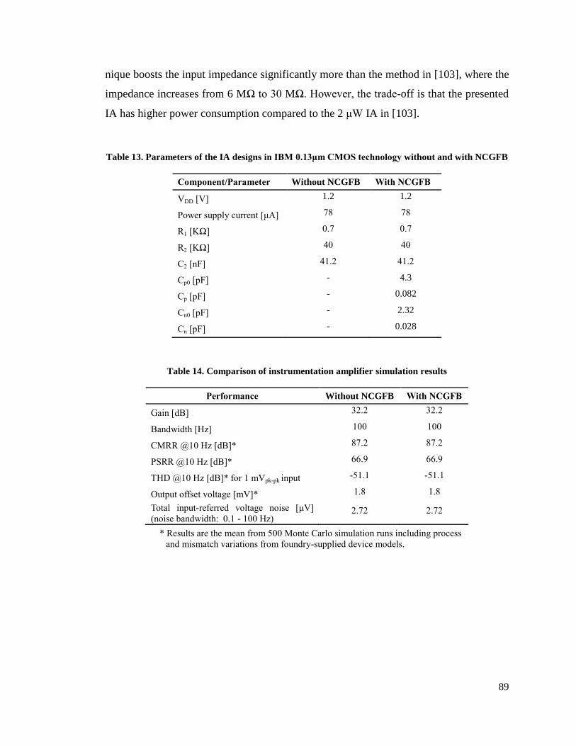
89
nique boosts the input impedance significantly more than the method in [103], where the
impedance increases from 6 MΩ to 30 MΩ. However, the trade-off is that the presented
IA has higher power consumption compared to the 2 μW IA in [103].
Table 13. Parameters of the IA designs in IBM 0.13μm CMOS technology without and with NCGFB
Component/Parameter Without NCGFB With NCGFB
VDD [V] 1.2 1.2
Power supply current [μA] 78 78
R1 [KΩ] 0.7 0.7
R2 [KΩ] 40 40
C2 [nF] 41.2 41.2
Cp0 [pF] - 4.3
Cp [pF] - 0.082
Cn0 [pF] - 2.32
Cn [pF] - 0.028
Table 14. Comparison of instrumentation amplifier simulation results
Performance Without NCGFB With NCGFB
Gain [dB] 32.2 32.2
Bandwidth [Hz] 100 100
CMRR @10 Hz [dB]* 87.2 87.2
PSRR @10 Hz [dB]* 66.9 66.9
THD @10 Hz [dB]* for 1 mVpk-pk input -51.1 -51.1
Output offset voltage [mV]* 1.8 1.8
Total input-referred voltage noise [μV]
(noise bandwidth: 0.1 - 100 Hz) 2.72 2.72
* Results are the mean from 500 Monte Carlo simulation runs including process
and mismatch variations from foundry-supplied device models.

90
0
40
80
120
160
120 13070 80 90 100 110
mu = 87.1528sd = 9.50065N = 500
80
120
160
0
40
120 13070 80 90 100 110
mu = 87.1502sd = 9.48983N = 500
(a) (b)
0
50
100
150
200
50 60 70 80 90 100
mu = 66.8856sd = 7.2409N = 500
0
50
100
150
200
10050 60 70 80 90
mu = 66.8855sd = 7.24242N = 500
(c) (d)
200
0
40
80
120
160
600 700 800(m)100 200 300 400 500
mu = 280.492msd = 100.826mN = 500
0
40
80
120
160
200
600 700500(m)100 200 300 400 800
mu = 280.493msd = 100.826mN = 500
(e) (f)
Figure 63. Monte Carlo simulation results of both IAs.
CMRR: (a) IA without NCGFB and (b) IA with NCGFB,
PSRR: (c) IA without NCGFB and (d) IA with NCGFB,
THD: (e) IA without NCGFB and (f) IA with NCGFB.

91
V/s
qrt
(Hz)
(u
V/s
qrt
(Hz)
)
1.5
2
2.5
3
0
0.5
1
freq (Hz)100 1k0.1 1 10
0
0.5
1
1.5
2
2.5
3
V/s
qrt
(Hz)
(u
V/s
qrt
(Hz)
)
1 10freq (Hz)
0.1 100 1k
(a) (b)
Figure 64. Noise distributions: (a) IA without NCGFB, (b) IA with NCGFB.
(a)
(b) Figure 65. Impedances at the IA inputs with and without NCGFB for different Csp and Csn values: (a)
Csp = Csn = 100 pF, (b) Csp = 200 pF and Csn = 50 pF.

92
Figure 66. Input impedance comparison (at Zinp) for the IAs with and without NCGFB in different
process corner cases.
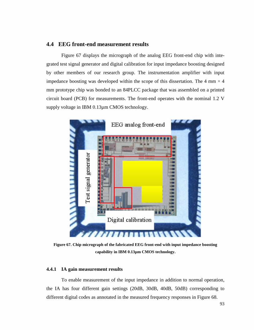
93
4.4 EEG front-end measurement results
Figure 67 displays the micrograph of the analog EEG front-end chip with inte-
grated test signal generator and digital calibration for input impedance boosting designed
by other members of our research group. The instrumentation amplifier with input
impedance boosting was developed within the scope of this dissertation. The 4 mm × 4
mm prototype chip was bonded to an 84PLCC package that was assembled on a printed
circuit board (PCB) for measurements. The front-end operates with the nominal 1.2 V
supply voltage in IBM 0.13µm CMOS technology.
Figure 67. Chip micrograph of the fabricated EEG front-end with input impedance boosting
capability in IBM 0.13µm CMOS technology.
4.4.1 IA gain measurement results
To enable measurement of the input impedance in addition to normal operation,
the IA has four different gain settings (20dB, 30dB, 40dB, 50dB) corresponding to
different digital codes as annotated in the measured frequency responses in Figure 68.
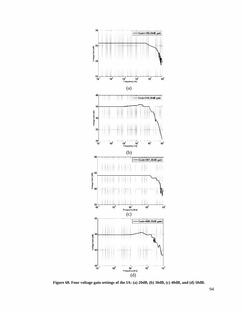
94
(a)
(b)
(c)
(d)
Figure 68. Four voltage gain settings of the IA: (a) 20dB, (b) 30dB, (c) 40dB, and (d) 50dB.
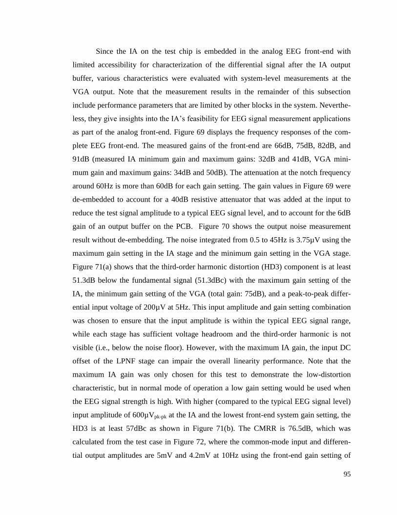
95
Since the IA on the test chip is embedded in the analog EEG front-end with
limited accessibility for characterization of the differential signal after the IA output
buffer, various characteristics were evaluated with system-level measurements at the
VGA output. Note that the measurement results in the remainder of this subsection
include performance parameters that are limited by other blocks in the system. Neverthe-
less, they give insights into the IA’s feasibility for EEG signal measurement applications
as part of the analog front-end. Figure 69 displays the frequency responses of the com-
plete EEG front-end. The measured gains of the front-end are 66dB, 75dB, 82dB, and
91dB (measured IA minimum gain and maximum gains: 32dB and 41dB, VGA mini-
mum gain and maximum gains: 34dB and 50dB). The attenuation at the notch frequency
around 60Hz is more than 60dB for each gain setting. The gain values in Figure 69 were
de-embedded to account for a 40dB resistive attenuator that was added at the input to
reduce the test signal amplitude to a typical EEG signal level, and to account for the 6dB
gain of an output buffer on the PCB. Figure 70 shows the output noise measurement
result without de-embedding. The noise integrated from 0.5 to 45Hz is 3.75µV using the
maximum gain setting in the IA stage and the minimum gain setting in the VGA stage.
Figure 71(a) shows that the third-order harmonic distortion (HD3) component is at least
51.3dB below the fundamental signal (51.3dBc) with the maximum gain setting of the
IA, the minimum gain setting of the VGA (total gain: 75dB), and a peak-to-peak differ-
ential input voltage of 200µV at 5Hz. This input amplitude and gain setting combination
was chosen to ensure that the input amplitude is within the typical EEG signal range,
while each stage has sufficient voltage headroom and the third-order harmonic is not
visible (i.e., below the noise floor). However, with the maximum IA gain, the input DC
offset of the LPNF stage can impair the overall linearity performance. Note that the
maximum IA gain was only chosen for this test to demonstrate the low-distortion
characteristic, but in normal mode of operation a low gain setting would be used when
the EEG signal strength is high. With higher (compared to the typical EEG signal level)
input amplitude of 600µVpk-pk at the IA and the lowest front-end system gain setting, the
HD3 is at least 57dBc as shown in Figure 71(b). The CMRR is 76.5dB, which was
calculated from the test case in Figure 72, where the common-mode input and differen-
tial output amplitudes are 5mV and 4.2mV at 10Hz using the front-end gain setting of
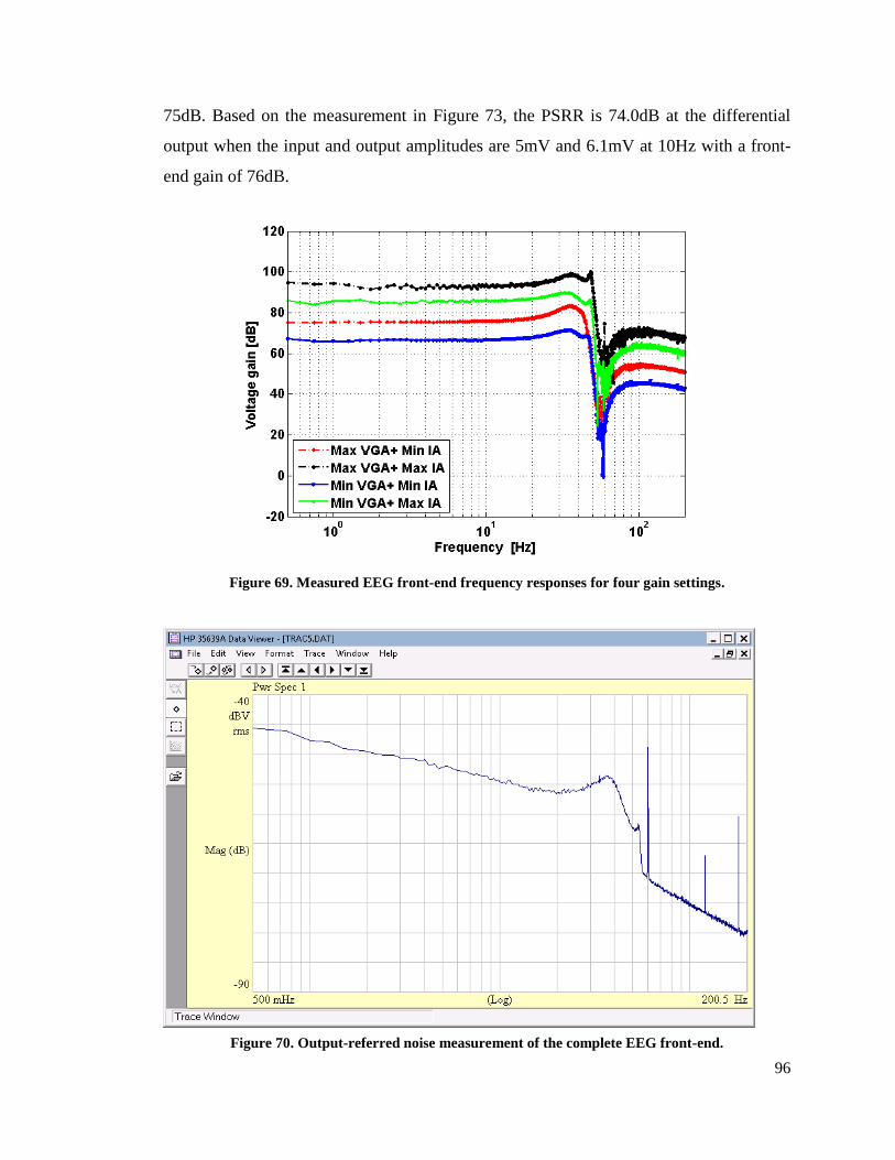
96
75dB. Based on the measurement in Figure 73, the PSRR is 74.0dB at the differential
output when the input and output amplitudes are 5mV and 6.1mV at 10Hz with a front-
end gain of 76dB.
Figure 69. Measured EEG front-end frequency responses for four gain settings.
Figure 70. Output-referred noise measurement of the complete EEG front-end.

97
(a)
(b)
Figure 71. HD3 measurement at 15Hz with a 5Hz sinusoidal input having a differential amplitude of
(a) 200μV, and (b) 600μV.

98
Figure 72. Input common-mode gain measurement: differential front-end output spectrum during a
test with a 5mV sinusoidal common-mode input signal at 10Hz.
Figure 73. Power supply gain measurement: differential front-end output spectrum during a test
with a 5mV sinusoidal signal injected at the power supply rail with a frequency of 10Hz.
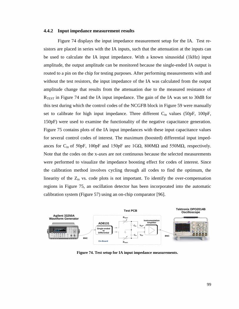
99
4.4.2 Input impedance measurement results
Figure 74 displays the input impedance measurement setup for the IA. Test re-
sistors are placed in series with the IA inputs, such that the attenuation at the inputs can
be used to calculate the IA input impedance. With a known sinusoidal (1kHz) input
amplitude, the output amplitude can be monitored because the single-ended IA output is
routed to a pin on the chip for testing purposes. After performing measurements with and
without the test resistors, the input impedance of the IA was calculated from the output
amplitude change that results from the attenuation due to the measured resistance of
RTEST in Figure 74 and the IA input impedance. The gain of the IA was set to 30dB for
this test during which the control codes of the NCGFB block in Figure 59 were manually
set to calibrate for high input impedance. Three different Cin values (50pF, 100pF,
150pF) were used to examine the functionality of the negative capacitance generation.
Figure 75 contains plots of the IA input impedances with these input capacitance values
for several control codes of interest. The maximum (boosted) differential input imped-
ances for Cin of 50pF, 100pF and 150pF are 1GΩ, 800MΩ and 550MΩ, respectively.
Note that the codes on the x-axes are not continuous because the selected measurements
were performed to visualize the impedance boosting effect for codes of interest. Since
the calibration method involves cycling through all codes to find the optimum, the
linearity of the Zin vs. code plots is not important. To identify the over-compensation
regions in Figure 75, an oscillation detector has been incorporated into the automatic
calibration system (Figure 57) using an on-chip comparator [96].
Instrumentation Amplifier
Single-ended to
Differential
Cin
Cin
RTEST
RTESTOn-Board
VIN+
VIN-
BNCBNC
Agilent 33250AWaveform Generator
Test PCBTektronix DPO2014B
Oscilloscope
AD8131
Figure 74. Test setup for IA input impedance measurements.

100
Figure 75. Input impedances vs. different codes: (a) Cin= 50pF, (b) Cin= 100pF, and (c) Cin = 150pF.

101
4.5 Conclusion
This chapter described an input impedance boosting technique for integrated in-
strumentation amplifiers. Designed in IBM 0.13μm CMOS technology, the negative
capacitance generation feedback of the instrumentation amplifier can increase its differ-
ential impedance from below 40MΩ to above 500MΩ at 50Hz after the proper
adjustment of digitally programmable capacitors when the input equivalent capacitor is
equal to 150pF. Based on the measured results, the important performance parameters
such as noise, CMRR, PSRR, and HD3 are not significantly affected by the proposed
input capacitance cancellation technique.
102
5. General Conclusion and Future Work
This dissertation research concentrated on two fundamental research topics, low-
power RF front-end design with linearization techniques and instrumentation amplifier
(IA) design with input impedance boosting for dry-contact EEG measurement applica-
tions. With regards to low-power RF design, two subthreshold linearized LNAs and one
subthreshold linearized RF front-end (LNA and mixer combination) were measured with
sub-microwatt power consumptions. The experimental results validated that the pro-
posed methods can improve IIP3 specifications by at least 10dB. The linearization
methods do not require an auxiliary amplifier to enhance linearity, making them suitable
for low-power narrow-band wireless standards. Investigations of the new input imped-
ance boosting technique revealed that the IA with programmable capacitor array can
generate the negative capacitive impedance required to cancel the capacitance from
printed circuit boards and cables. The measured results demonstrated that the input
impedance boosting technique is efficient and does not cause extra power consumption.
Continuous improvement of other RF performance specifications such as noise fig-
ure is remaining a research topic of interest in the area of low-power RF design.
Furthermore, future research could involve the extension of the low-power design and
linearization approaches from this dissertation to analog filters and amplifiers in the
baseband section of integrated receivers. The digital tunability characteristics of the low-
noise amplifier make it suitable for systems-on-a-chip with on-chip digital performance
monitoring for automatic calibration, which is another area with extensive research
opportunities. In relation to the instrumentation amplifier within the front-end for EEG
signal monitoring applications, our research group will continue the testing of the system
for automatic on-chip calibration using the on-chip test signal generator together with
the digital control circuits on the chip.

103
6. Appendices
6.1 Appendix A
The following equations can be written after applying Kirchhoff’s current law to nodes 1,
2, and 3 in Figure 8:
01
3211
11
VCjVCjV
ZCjCjCj
Z
Vgdgsgbgdgs
x , (A.1)
01
2
2
1
dgsgsiV
ZCjVCj , (A.2)
01
3
3
1
dgdgdiV
ZCjVCj . (A.3)
Furthermore,
21
VVVgs
. (A.4)
Using (A.1) through (A.4) and the definitions of g(ω) and Z3(ω) in Section 2.2.1, Vgs(ω)
can be derived as the following function of Vx and id:
d
xgd
gsi
Z
VZCj
gV
311 . (A.5)
The relation between Vx and V3, where Vx and V3 are the input and output voltages of
the input stage with the CS amplifier, can be expressed with a Volterra series as
...,,,321321213 xxx
VCVCVCV . (A.6)
On the other hand, the relationship between the drain current (id) and the gate voltage
(Vgs) of the CS amplifier can be written in terms of its linear transconductance (g1) and
its nonlinear transconductance components (g2, g3,…):
...3
3
2
21
gsgs
VgVgVgVigsgsd
. (A.7)
Furthermore, the relation between Vx and Vgs in Figure 8 can also be expressed with a
Volterra series as
...,,,32132121 xxxgs
VAVAVAV . (A.8)
From [40]-[42], the linear transfer functions A1(ω) and C1(ω) above can be determined
by applying a single tone [Vx(ω) = ejωt
] in the analysis, which results in:
Z
ZCj
ggA
gd 3
1
1
11 , (A.9)

104
)()(
)()()()(11
31
ZCjcb
AgeddCjZC
gs
gd
; (A.10)
where
3
1 ZCjbgd
, (A.11)
13
2][ ZZCCCjCjCjc
gbgdgbgdgs , (A.12)
2
1 ZCjdgs
, (A.13)
12
2][ ZZCCCjCjCje
gbgsgbgdgs . (A.14)
6.2 Appendix B
By applying Kirchhoff’s current law to nodes 1 and 2 in Figure 9, the following
equations can be obtained:
0
32
2
2
12 VVCj
Z
VVVCj
gdgs
, (B.1)
0
3
3
23
dgdi
Z
VVVCj
. (B.2)
It is noted that
12
VVVgs
. (B.3)
From (B.1) through (B.3) and the g(ω) and Z2(ω) definitions in Chapter 2, Vgs(ω) can be
found in terms of V1 and id as follows:
d
gd
gsi
ZZCj
Vf
gV
32
1)(1 , (B.4)
where
322
2
23]1[1 ZZCZCjZCjf
gdgdgd . (B.5)
The relationship between V21 and V23 in Figure 9, where V1 and V3 are the input and
output voltages of the CG amplifier, can be written with Volterra series:
...,,,132131212113
VCVCVCV . (B.6)
The relation between the drain current (id) and the gate voltage (Vgs) of the CG amplifier
is
...3
3
2
21
gsgs
VgVgVgVigsgsd
. (B.7)

105
Furthermore, the relationship between V1 and Vgs can be expressed by applying Volterra
series as
...,,,32132121 xxxgs
VAVAVAV . (B.8)
Correspondingly, the linear transfer functions A1(ω) and C1(ω) can be determined
through single-tone analysis [using V1(ω) = ejωt
], which are:
321
1
1
ZZCj
f
ggA
gd
, (B.9)
f
ZCC
f
CjCjAgZC
gdgsgdgs 2
2
1131
1 . (B.10)
6.3 Appendix C
The effective transconductance and output impedance for the Miller approximation
in equation (19) can be derived from the small-signal model in Figure 14 as:
1
1
1
11
11
1
11
1
)11
(
gd
gs
so
mbm
mbgs
o
gs
s
m
effmsC
sCsLZ
gg
gsCZ
sC
sL
g
G
, (C.1)
1
2
111
1
1
211
))(1(//
1//
gss
ombms
o
gd
MoutCLs
ZggsLZ
sCZZ . (C.2)
Notice that Zo1 = ro1||1/(sCds1) in the above equation. From Figure 14, the input
impedance Zin’ can be determined as follows:
11
1
2
1
1
1111
1
1
11
1'
omb
o
s
gs
m
s
ombsDo
o
s
gs
inZg
Z
sL
C
gL
ZgsLZZ
ZsL
sCZ , (C.3)
where: 1
21)/11(
1//
gdv
MDsCA
ZZ
.
6.4 Appendix D
The Matlab script in this appendix can be used to determine the values of Ls and
Lg for input impedance matching based on specified operating point parameters and
parasitic capacitances. Generally, the LNA can be first designed according to gain, noise

106
figure, linearity, and/or other specifications of interest prior to obtaining parasitic
capacitances and other parameters for the script from the simulated operating point
information.
W0 = 2*pi*2.4e9; s = i*W0; Rs = 50;
gm2 = 9.86634e-3; gmb2 = 1.52424e-3; Gm2 = gm2+gmb2;
gm1 = 9.77958e-3; gmb1 = 2.40401e-3; rg1 = 4.33468;
Cgb1 = 65.5032e-15; Cgd1 = 1.0156e-013;
Cgs1 = 1.5951e-013;
for Ls = 0.5e-9:5e-11:5e-9
Zin1 = 1/(s*Cgs1)+s*Ls+Ls*gm1/Cgs1;
Gm1_eff = (gm1-s^2*Ls*Cgs1*gmb1) /(1+s*Ls*(gm1+gmb1+s*Cgs1))-s*Cgd1;
Zout1 = 1/(Gm2+s*Cgd1);
Cmf = (1+Gm1_eff*Zout1)*Cgd1+Cgb1;
if abs(real(1/(1/Zin1+s*Cmf)+rg1-Rs)/(Rs-rg1)) < 0.005
break
end
end
for Lg = 5e-9:5e-11:15e-9
Zin = s*Lg+rg1+1/(1/Zin1+s*Cmf);
if abs(imag((Zin)/(Rs))) < 0.005
break
end
end
display(Ls); display(Lg);
107
7. References
[1] Y. Li, B. Bakkalouglu, and C. Charabarti, “A system level energy model and
energy quality evaluation for integrated transceiver front-ends,” IEEE Trans. on
Very Large Scale Integration (VLSI) systems, vol. 15, no. 1, pp. 90–103, Jan.
2007.
[2] E. Callaway, P. Gorday, L. Hester, J. A. Gutierrez, M. Naeve, B. Heile, and V.
Bahl, “Home networking with IEEE 802.15.4: a developing standard for low-rate
wireless personal area networks,” IEEE Communications Magazine, vol. 40, no.
8, pp. 70–77, Aug. 2002.
[3] N.-J. Oh and S.-G. Lee, “Building a 2.4-GHz radio transceiver using IEEE
802.15.4,” IEEE Circuits and Devices Magazine, vol. 21, no. 6, pp. 43–51,
Nov./Dec. 2005.
[4] T.-K. Nguyen, N.-J. Oh, V.-H. Le, and S.-G. Lee, “A low-power CMOS direct
conversion receiver with 3-dB NF and 30-kHz Flicker-noise corner for 915-MHz
band IEEE 802.15.4 ZigBee standard,” IEEE Trans. on Microwave Theory and
Techniques, vol. 54, no. 2, pp. 735-741, Feb. 2006.
[5] A. Balankutty, S.-A. Yu, Y. Feng, and P. R. Kinget, “A 0.6-V zero-IF/low-IF
receiver with integrated fractional-N synthesizer for 2.4-GHz ISM-band applica-
tions,” IEEE J. Solid-state Circuits, vol. 45, no. 3, pp. 538–553, Mar. 2010.
[6] W. Rhee, N. Xu, B. Zhou, and Z. Wang, “Low power, non invasive UWB systems
for WBAN and biomedical applications,” in Proc. Int. Conf. on Information and
Communication Technology Convergence (ICTC), pp. 35–40, Nov. 2010.
[7] M. Contaldo, B. Banerjee, D. Ruffueux, J. Chabloz, E. L. Roux, and C. C. Enz,
“A 2.4-GHz BAW-based transceiver for wireless body area networks,” IEEE
Trans. on Biomedical Circuits and Systems, vol. 4, no. 6, pp. 391–399, Dec. 2010.
[8] M. A. Ameen, J. Liu, S. Ullah, and K. S. Kwak, “A power efficient MAC protocol
for implant device communication in wireless body area networks,” in Proc. IEEE
Consumer Communications and Networking Conf. (CCNC), pp. 1155–1160, Jan.
2011.
[9] N. E. Roberts, S. Oh, and D. D. Wentzloff, “Exploiting channel periodicity in
body sensor networks,” IEEE Trans. on Emerging and Selected Topics in Circuits
and Systems, vol. 2, no. 1, pp. 4–13, Mar. 2012.
[10] Y.-H. Liu, X. Huang, M. Vidojkovic, G. Domans, and H. de Groot, “An energy-
efficient polar transmitter for IEEE 802.15.6 body area networks: system require-
ments and circuit designs,” IEEE Communications Magazine, vol. 50, no. 10, pp.
118–127, Oct. 2012.
[11] A. C. W. Wong, M. Dawkins, G. Devita, N. Kasparidis, A. Katsiamis, O. King, F.
Lauria, J. Schiff, and A. J. Burdett, “A 1 V 5 mA Multimode IEEE
802.15.6/Bluetooth low-energy WBAN transceiver for biotelemetry applications,”
IEEE J. Solid-state Circuits, vol. 48, no. 1, pp. 186–198, Jan. 2013.
[12] D. B. Smith, D. Miniutti, T. A. Lamahwwa, and L. W. Hanlen, “Propagation
models for body-area networks: a survey and new outlook,” IEEE Antennas and
Propagation Magazine, vol. 55, no. 5, pp. 97–117, Oct. 2013.

108
[13] J. Masuch and M. Delgado-Restituto, “A 1.1-mW-RX -81.4-dBm sensitivity
CMOS transceiver for Bluetooth low energy,” IEEE Trans. on Microwave Theory
and Techniques, vol. 61, no. 4, pp. 1660–1673, Apr. 2013.
[14] C. Y. Leong, K. C. Ong, K. K. Tan, and O. P. Gan, “Near field communication
and Bluetooth bridge system for mobile commerce,” in Proc. IEEE Int. Conf. on
Industrial Informatics, pp. 50–55, Aug. 2006.
[15] J. Fischer, “NFC in cell phones: the new paradigm for an interactive world,” IEEE
Communications Magazine, vol. 47, no. 6, pp. 22–28, June 2009.
[16] A. R. Shahani, D. K. Shaeffer, and T. H. Lee, “A 12-mW wide dynamic range
CMOS front-end for a portable GPS receiver,” IEEE J. Solid-state Circuits, vol.
32, no. 12, pp. 2061–2070, Dec. 1997.
[17] D. K. Shaeffer, A. R. Shahani, S. S. Mohan, H. Samavati, H. R. Rategh, M. del M.
Hershenson, M. Xu, C. P. Yue, D. J. Eddleman, and T. H. Lee, “A 115-mW, 0.5-
µm CMOS GPS receiver with wide dynamic-range active filters,” IEEE J. Solid-
state Circuits, vol. 33, no. 12, pp. 2219–2231, Dec. 1998.
[18] F. Behbahani, H. Firouzkouhi, R. Chokkalingam, S. Delshadpour, A. Kheirkhahi,
M. Nariman, M. Conta, and S. Bhatia, “A fully integrated low-IF CMOS GPS ra-
dio with on-chip analog image rejection,” IEEE J. Solid-state Circuits, vol. 37, no.
12, pp. 1721–1727, Dec. 2002.
[19] T. Kadoyama, N. Suzuki, N. Sasho, H. Iizuka, I. Nagase, H. Usukubo, and M.
Katakura, “A complete single-chip GPS receiver with 1.6-V 24-mW radio in 0.18-
µm CMOS,” IEEE J. Solid-state Circuits, vol. 39, no. 4, pp. 562–568, Apr. 2004.
[20] J. Ko, J. kim, S. Cho, and K. Lee, “A 19-mW 2.6-mm2 L1/L2 dual-band CMOS
GPS receiver,” IEEE J. Solid-state Circuits, vol. 40, no. 7, pp. 1414–1425, July
2005.
[21] G. Gramegna, P. G. Mattos, M. Losi, S. Das, M. Franciotta, N. G. Bellantone, M.
Vaiana, V. Mandara, and M. Paparo, “A 56-mW 23-mm2 single-chip 180-nm
CMOS GPS receiver with 27.2-mW 4.1-mm2 radio,” IEEE J. Solid-state Circuits,
vol. 41, no. 3, pp. 540–551, Mar. 2006.
[22] A. C. Heiberg, T. W. Brown, T. S. Fiez, and K. Mayaram, “A 250mV, 352 µW
GPS receiver RF front-end in 130 nm CMOS,” IEEE J. Solid-state Circuits, vol.
46, no. 4, pp. 938–949, Apr. 2011.
[23] A. V. Do, C. C. Boon, M. A. Do, K. S. Yeo, and A. Cabuk, “A subthreshold low-
noise amplifier optimized for ultra-low-power applications in the ISM band,”
IEEE Trans. on Microwave Theory and Techniques, vol. 56, no. 2, pp. 286-292,
Feb. 2008.
[24] H. Lee and S. Mohammadi, “A 3GHz subthreshold CMOS low noise amplifier,”
in Proc. Radio Frequency Integrated Circuit (RFIC) Symp., June 2006.
[25] T. Taris, J. Begueret, and Y. Deval, “A 60µW LNA for 2.4 GHz wireless sensors
network applications,” in Proc. Radio Frequency Integrated Circuit (RFIC) Symp.,
June 2011.
[26] A. Shameli and P. Heydari, “A novel ultra low power low noise amplifier using
differential inductor feedback,” in Proc. IEEE European Solid State Circuit Conf.
(ESSCIRC), pp. 352-355, June 2011.
109
[27] A. V. Do, C. C. Boom, M. A. Do, K. S. Yeo, and A. Cabuk, “A weak-inversion
low-power active mixer for 2.4 GHz ISM band applications,” IEEE Microwave
and Wireless Components Letters, vol. 19, no. 11, pp. 719-721, Nov. 2009.
[28] R. F. Yazicioglu, P. Merken, R. Puers, and C. Van Hoof, “A 60 µW 60 nV/√Hz
readout front-end for portable biopotential acquisition systems,” IEEE J. Solid-
State Circuits, vol. 42, no. 5, pp. 1100-1110, May 2007.
[29] N. Verma, A. Shoeb, J. Bohorquez, J Dawson, J. Guttag, and A. P. Chandrakasan,
“A micro-power EEG acquisition SoC with integrated feature extraction processor
for a chronic seizure detection system,” IEEE J. Solid-State Circuits, vol. 45, no.
4, pp. 804-816, April 2010.
[30] J. Xu, R. F. Yazicioglu, P. Harpe, K. A. A. Makinwa, and C. Van Hoof, "A
160μW 8-channel active electrode system for EEG," in IEEE Intl. Solid-State Cir-
cuits Conf. (ISSCC) Dig. Tech. Papers, pp. 300-302, Feb. 2011.
[31] A. Casson, D. Yates, S. Smith, J. Duncan, and E. Rodriguez-Villegas, “Wearable
electroencephalography,” IEEE Engineering in Medicine and Biology Magazine,
vol. 29, no. 3, pp. 44 - 56 , May-June 2010.
[32] Y. M. Chi, T.-P. Jung, and G. Cauwenberghs, “Dry-contact and noncontact
biopotential electrodes: methodological review,” IEEE Reviews in Biomedical
Engineering, vol. 3, no. 1, pp. 106-119, Oct. 2010.
[33] C. Assambo and M. J. Burke, “Amplifier input impedance in dry electrode ECG
recording,” in Proc. Annual IEEE Conf. Engineering in Medicine and Biology So-
ciety (EMBC), pp. 1774-1777, Sept. 2009.
[34] H. Chauhan, Y. Choi, M. Onabajo, I.-S. Jung, and Y.-B. Kim, “Accurate and
efficient on-chip spectral analysis for built-in testing and calibration approaches,”
IEEE Trans. on Very Large Scale Integration (VLSI) Systems, vol. 22, no. 3, pp.
497-506, March 2014.
[35] Y. Choi, C.-H. Chang, H. Chauhan, I.-S. Jung, M. Onabajo, and Y.-B. Kim, “A
built-in calibration system to optimize third-order intermodulation performance of
RF amplifiers,” in Proc. IEEE Intl. Midwest Symp. on Circuits and Systems
(MWSCAS), pp. 599-602, Aug. 2014.
[36] D. Flandre, A. Viviani, J.P. Eggermont, B. Gentinne, and P G. A. Jespers, “Im-
proved synthesis of gain-boosted regulated-cascode CMOS stages using symbolic
analysis and gm/ID methodology,” IEEE J. Solid-state Circuits, vol. 32, no. 7, pp.
1006–1012, July 1997.
[37] B. Razavi, Design of Analog CMOS Integrated Circuits. McGraw-Hill Sci-
ence/Engineering/Math, 1st edition, 2000.
[38] D. D. Weiner and J. F. Spina, Sinusoidal Analysis And Modeling of Weakly
Nonlinear Circuits. New York: Van Nostrand Reinhold, 1980.
[39] H. Zhang and E. Sánchez-Sinencio, “Linearization techniques for CMOS low
noise amplifiers: a tutorial,” IEEE Trans. Circuits and Systems I: Regular Papers,
vol. 58, no. 1, pp. 22-36, Jan. 2011.
[40] V. Aparin, “Linearization of CDMA receiver front-ends,” Ph.D. dissertation, Univ.
California, San Diego, CA, USA, 2005.
110
[41] V. Aparin and L. E. Larson, “Modified derivative superposition method for
linearizing FET low-noise amplifier,” IEEE Trans. on Microwave Theory and
Techniques, vol. 53, no. 2, pp. 571-581, Feb. 2005.
[42] X. Fan, H. Zhang, and E. Sánchez-Sinencio, “A noise reduction and linearity
improvement technique for a differential cascode LNA,” IEEE J. Solid-state Cir-
cuits, vol. 43, no. 3, pp. 588-599, March 2008.
[43] H. Sjoland, J. B. Anderson, C. Bryant, R. Chandra, O. Edfors, A. J. Johansson, N.
S. Mazloum, R. Meraji, P. Nilsson, D. Radjen, J. N. Rodrigues, and S. M. Y.
Sherazi, “A receiver architecture for devices in wireless body area networks,”
IEEE J. Emerging and Selected Topics in Circuits and Systems, vol. 2, no. 1, pp.
82-95, Jan. 2012.
[44] M. Contaldo, B. Banerjee, D. Ruffieux, J. Chabloz, E. Le Roux, and C. C. Enz,
“A 2.4-GHz BAW-based transceiver for wireless body area networks,” IEEE
Trans. Biomedical Circuits and Systems, vol. 5, no. 6, pp. 391-399, Jun. 2010.
[45] D. Han, B. S. Kim, and A. Chatterjee, “DSP-driven self-tuning of RF circuits for
process-induced performance variability,” IEEE Trans. Very Large Scale Integra-
tion (VLSI) Systems, vol. 18, no. 2, pp. 305-314, Feb. 2010.
[46] D. Kaczman, M. Shah, M. Alam, M. Rachedine, D. Cashen, L. Han, and A.
Raghavan, “A single-chip 10-band WCDMA/HSDPA 4-band GSM/EDGE SAW-
less CMOS receiver with DigRF 3G interface and +90 dBm IIP2,” IEEE J. Solid-
State Circuits, vol. 44, no. 3, pp. 718-739, Mar. 2009.
[47] Y. Feng, G. Takemura, S. Kawaguchi, N. Itoh, and P. R. Kinget, “Digitally
assisted IIP2 calibration for CMOS direct-conversion receivers,” IEEE J. Solid-
State Circuits, vol. 46, no. 10, pp. 2253-2267, Oct. 2011.
[48] G. Banerjee, M. Behera, M. A. Zeidan, R. Chen, and K. Barnett, “Analog/RF
built-in-self-test subsystem for a mobile broadcast video receiver in 65-nm
CMOS,” IEEE J. Solid-State Circuits, vol. 46, no. 9, pp. 1998-2008, Sep. 2011.
[49] H. Darabi, J. Chiu, S. Khorram, H. J. Kim, Z. Zhou, H.-M. Chien, B. Ibrahim, E.
Geronaga, L. H. Tran, and A. Rofougaran, “A dual-mode 802.11b/Bluetooth radio
in 0.35-μm CMOS,” IEEE J. Solid-State Circuits, vol. 40, no. 3, pp. 698-706,
Mar. 2005.
[50] A. Goyal, M. Swaminathan, A. Chatterjee, D. C. Howard, and J. D. Cressler, “A
new self-healing methodology for RF amplifier circuits based on oscillation prin-
ciples,” IEEE Trans. Very Large Scale Integration (VLSI) Systems, vol. 20, no.
10, pp. 1835-1848, Oct. 2012.
[51] E. Maricau and G. Gielen, “Computer-aided analog circuit design for reliability in
nanometer CMOS,” IEEE J. Emerging and Selected Topics in Circuits and Sys-
tems, vol. 1, no. 1, pp. 50-58, Jan. 2011.
[52] I. Vassiliou, K. Vavelidis, T. Georgantas, S. Plevridis, N. Haralabidis, G. Kamou-
lakos, C. Kapnistis, S. Kavadias, Y. Kokolakis, P. Merakos, J. C. Rudell, A.
Yamanaka, S. Bouras, and I. Bouras, “A single-chip digitally calibrated 5.15-
5.825-GHz 0.18-μm CMOS transceiver for 802.11a wireless LAN,” IEEE J. Sol-
id-State Circuits, vol. 38, no. 12, pp. 2221-2231, Dec. 2003.

111
[53] M. Mobarak, M. Onabajo, J. Silva-Martinez, and E. Sánchez-Sinencio, “Attenua-
tion- predistortion linearization of CMOS OTAs with digital correction of process
variations in OTA-C filter applications,” IEEE J. Solid-State Circuits, vol. 45, no.
2, pp. 351-367, Feb. 2010.
[54] S. Rodriguez, A. Rusu, L.-R. Zheng, and M. Ismail, “CMOS RF mixer with
digitally enhanced IIP2,” Electronics Letters, vol. 44, no. 2, pp. 121-122, Feb.
2008.
[55] C.-H. Liao and H.-R. Chuang, “A 5.7-GHz 0.18-μm CMOS gain-controlled
differential LNA with current reuse for WLAN receiver,” IEEE Microwave and
Wireless Components Letters, vol. 13, no. 12, pp. 526- 528, Dec. 2003.
[56] T. H. Lee, The Design of CMOS Radio-Frequency Integrated Circuits. Cam-
bridge, U.K.: Cambridge Univ. Press, 1998.
[57] X. Fan, M. Onabajo, F. O. Fernández-Rodríguez, J. Silva-Martinez, and E.
Sánchez-Sinencio, “A current injection built-in test technique for RF low-noise
amplifier,” IEEE Trans. Circuits and Systems I: Regular Papers, vol. 55, no. 7,
pp. 1794-1804, Jul. 2008.
[58] T. Das, A. Gopalan, C. Washburn, and P. R. Mukund, “Self-calibration of input-
match in RF front-end circuitry,” IEEE Trans. Circuits Syst. II: Express Briefs,
vol. 52, no. 12, pp. 821-825., Dec. 2005.
[59] J. Wilson, and M. Ismail, “Input match and load tank digital calibration of an
inductively degenerated CMOS LNA,” Integration, the VLSI Journal, vol. 42, no.
1, pp. 3-9., Jan. 2009.
[60] Y.-L. Lai and C.-Y. Ho, “Electrical modeling of quad flat no-lead packages for
high-frequency IC applications,” in Proc. IEEE Region 10 Conf. (TENCON), vol.
4, pp. 344-347, Nov. 2004.
[61] S. Asgaran, M. J. Deen, and C.-H. Chen, “Design of the input matching network
of RF CMOS LNAs for low-power operation,” IEEE Trans. Circuits and Systems
I: Regular Papers, vol. 54, no. 3, pp. 544 - 554, Mar. 2007.
[62] V. Subramanian, M. Krcmar, M. J. Deen, and G. Boeck, “A 6 GHz fully integrat-
ed SiGe LNA with simplified matching circuitries,” in Proc. European Wireless
Technology Conf. (EuWiT), pp. 17-20, Oct. 2008.
[63] R. Fiorelli, F. Silveria, and E. Peralias, “MOST moderate-weak-inversion region
as the optimum design zone for CMOS 2.4-GHz CS-LNAs,” IEEE Trans. on Mi-
crowave Theory and Techniques, vol. 62, no. 3, pp. 556-566, March 2014.
[64] S. H. M. Lavasani and S. Kiaei, “A new method to stabilize high frequency high
gain CMOS LNA,” in Proc. IEEE Intl. Conf. on Electronics, Circuits and Systems
(ICECS), vol. 3, pp. 982-985, Dec. 2003.
[65] C.-H. Chang and M. Onabajo, “Input impedance matching optimization for
adaptive low-power low-noise amplifiers,” Analog Integrated Circuits and Signal
Processing, vol. 77, no. 3, pp. 583-592, Dec. 2013.
[66] J. Yang, N. Tran, S. Bai, M. Fu, E. Skafidas, M. Halpern, D.C. Ng, and I. Mareels,
“A subthreshold down converter optimized for super-low-power applications in
MICS Band,” in Proc. IEEE Biomedical Circuits and Systems Conf. (BioCAS), pp.
189-192, Nov. 2011.

112
[67] R. Brederlow, W. Weber, J. Sauerer, S. Donnay, P. Wambacq, and M. Vertregt,
“A Mixed-signal design roadmap,” IEEE Design & Test of Computers, vol. 18, no.
6, pp. 34-46, Nov./Dec. 2001.
[68] B. G. Perumana, S. Chakraborty, C.-H. Lee, and J. Laskar, “A fully monolithic
260-µW, 1-GHz subthreshold low noise amplifier,” IEEE Microwave Theory and
Wireless Component Letters, vol. 15, no. 6, pp. 428-430, June 2005.
[69] B. Razavi, RF Microelectronics. Prentice Hall, 2nd edition, 2011.
[70] H. Lee and S. Mohammadi, “A 500μW 2.4GHz CMOS subthreshold mixer for
ultra low power application,” in Proc. Radio Frequency Integrated Circuits
(RFIC) Symp., pp. 325-328, June 2007.
[71] T.-K. Nguyen, V. Krizhanovskii, J. Lee, S.-K. Han, S.G. Lee, N-S. Kim, and C.-S.
Pyo, “A low-power RF direct-conversion receiver/transmitter for 2.4 GHz-band
IEEE 802.15.4 standard in 0.18-μm CMOS technology,” IEEE Transactions on
Microwave Theory and Techniques, vol. 54, no. 12, pp. 4062-4071, Dec. 2006.
[72] K. Wang, K. Ma, W. Ye, K. S. Yeo, H. Zhang, and Z. Wang, “A low voltage low
power highly linear CMOS quadrature mixer using transconductance cancellation
technique,” in IEEE Int. Microwave Symposium Digest (MTT), pp. 1-3, June
2012.
[73] J. T. Yang, Y. M. Mu, M. J. Wu, Y. H. Lee, and Y. Y. Huang, “A 2.4GHz low
power highly linear mixer for direct-conversion receivers,” Int. J. of Circuits, Sys-
tems and Signal Processing, vol. 1, no. 2, pp. 203-206, Dec. 2007.
[74] C.-H. Chang and M. Onabajo, "Linearization of subthreshold low-noise amplifi-
ers," in Proc. 2013 IEEE Intl. Symposium on Circuits and Systems (ISCAS), pp.
377-380, May 2013.
[75] T. Cho, E. Dukatz, M. Mack, D. MacNally, M. Marringa, S. Mehta, C. Nilson, L.
Plouvier, and S. Rabii, “A single-chip CMOS direct-conversion transceiver for
900MHz spread-spectrum digital cordless phones,” in IEEE Int. Solid-State Cir-
cuits Conf. (ISSCC) Dig. Tech. Papers, pp. 228-229, 1999.
[76] X. Li, S. Shekhar, and D. J. Allstot, “Gm-boosted common-gate LNA and differ-
ential Colpitts VCO/QVCO in 0.18-μm CMOS,” IEEE J. Solid-State Circuits, vol.
40, no. 12, pp. 2609-2619, Dec. 2005.
[77] W. Zhuo, S. Embabi, J. Gyvez, and E. Sanchez-Sinencio, “Using capacitive
cross-coupling technique in RF low-noise amplifiers and down-conversion mixer
design,” IEEE Proc. Eur. Solid-State Circuits Conf. (ESSCIRC), pp. 116–119,
Sep. 2000.
[78] W. Zhuo, X. Li, S. Shekhar, S. Embabi, J. Gyvez, D. J. Allstot and E. Sanchez-
Sinencio, “A capacitor cross-coupled common-gate low-noise amplifier,” IEEE
Trans. Circuits and Systems II: Express Briefs, vol. 52, no. 12, pp. 875-879, Dec.
2005.
[79] T. Li, F. Huang, J. Li, and X. Tang, “Design of a reconfigurable dual-band mixer
for IMT-A and UWB systems,” in Proc. IEEE Int. Conf. on Ultra-Wideband
(ICUWB), vol. 40, pp. 1-4, Sep. 2010.
113
[80] C.-H. Chang and M. Onabajo, "IIP3 enhancement of subthreshold active mixers,"
IEEE Trans. On Circuits and Systems II: Express Briefs, vol. 60, no. 11, pp. 731-
735, Nov. 2013.
[81] W. Yu, S. Sen, and B. H. Leung, “Distortion analysis of MOS track-and-hold
sampling mixers using time-varying Volterra series,” IEEE Trans. on Circuits and
Systems II: Analog and Digital Signal Processing, vol. 46, no. 2, pp. 101-113,
Feb. 1996.
[82] Q. Li and J. S. Yuan, “Linearity analysis and design optimisation for 0.18μm
CMOS RF mixer,” in IEE Proc. Circuits Devices and Systems, vol. 149, no. 2, pp.
112-118, April 2002.
[83] J. Kim and Y. Kwon, “Intermodulation analysis of dual-gate FET mixers,” IEEE
Trans. on Microwave Theory and Techniques, vol. 50, no. 6, pp. 1544-1555, June
2002.
[84] C. Yu, J. S. Yuan, and H. Yang, “MOSFET linearity performance degradation
subject to drain and gate voltage stress,” IEEE Trans. on Device and Materials
Reliability, vol. 4, no. 4, pp. 681-689, Dec. 2004.
[85] P. Sakain, R. Mahmoudi, and A. V. Roermund, “A circuit-level analysis of third
order intermodulation mechanisms in CMOS mixers using time-invariant power
and Volterra series,” in Proc. of the 41st European Microwave Conf., pp. 595-
598, Oct. 2011.
[86] Texas Instruments. Quad Flat No-Lead (QFN) Package Comparison Tables.
Available online: http://focus.ti.com/pdfs/logic/qfncompare.pdf
[87] C. Hermann, M. Tiebout and H. Klar, “A 0.6-V 1.6-mW transformer-based 2.5-
GHz downconversion mixer with +5.4-dB gain and -2.8-dBm IIP3 in 0.13-μm
CMOS,” IEEE Trans. Microwave Theory Tech., vol. 53, no. 2, pp. 488-495, Feb.
2005.
[88] V. Vidojkovic, J. V. D. Tang, A. Leeuwenburgh, and A. H. M. V. Roermund, “A
low-voltage folded-switching mixer in 0.18-μm CMOS,” IEEE J. Solid-State Cir-
cuits, vol. 40, no. 6, pp. 1259-1264, June 2005.
[89] M. Brandolini, P. Rossi, D. Sanzogni, and F. Svelto, “A +78 dBm IIP2 CMOS
direct downconversion mixer for fully integrated UMTS receivers,” IEEE J. Sol-
id-State Circuits, vol. 41, no. 3, pp. 552-559, June 2006.
[90] M. A. Abdelghany, P. K. Pokharel, H. Kanaya, and K. Yoshida, “Low-voltage
low-power combined LNA-single gate mixer for 5GHz wireless systems,” in
Proc. Radio Frequency Integrated Circuits (RFIC) Symp., pp. 1-4, June 2011.
[91] S.-Y. Lee, L.-H. Wang, T.-Y. Chen, and C.-T. Yu, "A low-power RF front-end
with merged LNA, differential power splitter, and quadrature mixer for IEEE
802.15.4 (ZigBee) applications," in Proc. 2012 IEEE Intl. Symposium on Circuits
and Systems (ISCAS), pp. 1492-1496, May 2012.
[92] R. Fiorelli, A. Villegas, E. Peralias, D. Vazquez, and A. Rueda, "2.4-GHz single-
ended input low-power-voltage active front-end for Zigbee applications in 90 nm
CMOS," in Proc. European Conference on Circuit Theory and Design (ECCTD),
pp. 829-832, May 2011.
114
[93] K.-H. Lin, T.-H. Yang, and C.-W. Hsu, "Implementation of a low-power folded-
cascode RF front-end for LTE receivers," in Proc. International Symposium on
Computer, Consumer and Control (IS3C), pp. 1049-1052, June 2014.
[94] K. Soundararajan and K. Ramakrishna, (1975) “Nonideal negative resistors and
capacitors using an operational amplifier,” Trans. on Circuits and Systems, vol.
22, no. 9, pp. 760-763, Sep. 1975.
[95] C.-H. Chang and M. Onabajo, “Instrumentation amplifier input capacitance
cancellation for biopotential and bioimpedance measurements,” in Proc. IEEE Intl.
Midwest Symp. on Circuits and Systems (MWSCAS), pp. 539-542, Aug. 2014.
[96] S. A. Zahrai, L. Xu, C.-H. Chang, K. Wang, I. Farah, and M. Onabajo, “On-chip
digital calibration for automatic input impedance boosting during biopotential
measurements”, in Proc. IEEE Intl. Midwest Symp. on Circuits and Systems
(MWSCAS), August 2015.
[97] Y. Ni and M. Onabajo, “A low-power temperature-compensated CMOS relaxa-
tion oscillator,” Analog Integrated Circuits and Signal Processing, vol. 79, no. 2,
pp. 309-317, Feb. 2014.
[98] L. Xu, J. Feng, Y. Ni, and M. Onabajo, “Test signal generation for the calibration
of analog front-end circuits in biopotential measurement applications,” in Proc.
IEEE Intl. Midwest Symp. on Circuits and Systems (MWSCAS), pp. 949-952, Aug.
2014.
[99] R. Martins, S. Selberherr, and F. A. Vaz, “A CMOS IC for portable EEG acquisi-
tion systems,” IEEE Trans. on Instrumentation and Measurement, vol. 47, no. 5,
pp. 1191-1196, May 1998.
[100] A. Worapishet, A. Demosthenous, and X. Liu, “A CMOS instrumentation ampli-
fier with 90-dB CMRR at 2-MHz using capacitive neutralization: analysis, design
considerations, and implementation,” IEEE Trans. on Circuits and Systems-I:
Regular Papers, vol. 58, no. 4, pp. 699-710, Apr. 2011.
[101] Y. Li, C. C. F. Poo, and Y.-T. Zhang, “Analog integrated circuits design for
processing physiological signals,” IEEE Reviews in Biomedical Engineering, vol.
3, pp. 93-105, Dec. 2010.
[102] Analog Devices. Precision Instrumentation Amplifier - AD8221. Online:
http://www.analog.com/static/imported-files/data_sheets/AD8221.pdf
[103] Q. Fan, F. Sebastiano, J. H. Huijsing, and K. A. A. Makinwa, “A 1.8 μW 60nV/
√Hz capacitively-coupled chopper instrumentation amplifier in 65 nm CMOS for
wireless sensor nodes,” IEEE J. Solid-State Circuits, vol. 46, no. 7, pp. 1534-
1543, Jul. 2011.