RADIATION EFFECTS
22
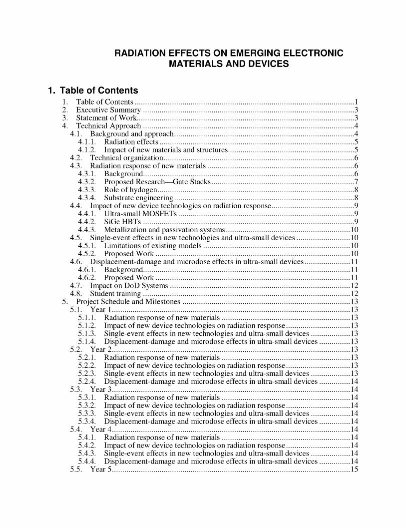
RADIATION EFFECTS ON EMERGING ELECTRONIC MATERIALS AND DEVICES 1. Table of Contents 1. Table of Contents ..........................................................................................................1 2. Executive Summary ......................................................................................................3 3. Statement of Work.........................................................................................................3 4. Technical Approach ......................................................................................................4 4.1. Background and approach.......................................................................................4 4.1.1. Radiation effects ..............................................................................................5 4.1.2. Impact of new materials and structures.............................................................5 4.2. Technical organization ............................................................................................6 4.3. Radiation response of new materials .......................................................................6 4.3.1. Background......................................................................................................6 4.3.2. Proposed Research—Gate Stacks .....................................................................7 4.3.3. Role of hydogen...............................................................................................8 4.3.4. Substrate engineering .......................................................................................8 4.4. Impact of new device technologies on radiation response........................................9 4.4.1. Ultra-small MOSFETs .....................................................................................9 4.4.2. SiGe HBTs ......................................................................................................9 4.4.3. Metallization and passivation systems ............................................................ 10 4.5. Single-event effects in new technologies and ultra-small devices .......................... 10 4.5.1. Limitations of existing models ....................................................................... 10 4.5.2. Proposed Work .............................................................................................. 10 4.6. Displacement-damage and microdose effects in ultra-small devices ...................... 11 4.6.1. Background.................................................................................................... 11 4.6.2. Proposed Work .............................................................................................. 11 4.7. Impact on DoD Systems ....................................................................................... 12 4.8. Student training .................................................................................................... 12 5. Project Schedule and Milestones ................................................................................. 13 5.1. Year 1................................................................................................................... 13 5.1.1. Radiation response of new materials .............................................................. 13 5.1.2. Impact of new device technologies on radiation response ............................... 13 5.1.3. Single-event effects in new technologies and ultra-small devices ................... 13 5.1.4. Displacement-damage and microdose effects in ultra-small devices ............... 13 5.2. Year 2................................................................................................................... 13 5.2.1. Radiation response of new materials .............................................................. 13 5.2.2. Impact of new device technologies on radiation response ............................... 13 5.2.3. Single-event effects in new technologies and ultra-small devices ................... 13 5.2.4. Displacement-damage and microdose effects in ultra-small devices ............... 14 5.3. Year 3................................................................................................................... 14 5.3.1. Radiation response of new materials .............................................................. 14 5.3.2. Impact of new device technologies on radiation response ............................... 14 5.3.3. Single-event effects in new technologies and ultra-small devices ................... 14 5.3.4. Displacement-damage and microdose effects in ultra-small devices ............... 14 5.4. Year 4................................................................................................................... 14 5.4.1. Radiation response of new materials .............................................................. 14 5.4.2. Impact of new device technologies on radiation response ............................... 14 5.4.3. Single-event effects in new technologies and ultra-small devices ................... 14 5.4.4. Displacement-damage and microdose effects in ultra-small devices ............... 14 5.5. Year 5................................................................................................................... 15
-
Upload
janderson13 -
Category
Documents
-
view
211 -
download
2
Transcript of RADIATION EFFECTS
RADIATION EFFECTS ON EMERGING ELECTRONIC MATERIALS AND DEVICES
1. Table of Contents 1. Table of Contents ..........................................................................................................1 2. Executive Summary ......................................................................................................3 3. Statement of Work.........................................................................................................3 4. Technical Approach ......................................................................................................4
4.1. Background and approach.......................................................................................4 4.1.1. Radiation effects ..............................................................................................5 4.1.2. Impact of new materials and structures.............................................................5
4.2. Technical organization............................................................................................6 4.3. Radiation response of new materials .......................................................................6
4.3.1. Background......................................................................................................6 4.3.2. Proposed Research—Gate Stacks.....................................................................7 4.3.3. Role of hydogen...............................................................................................8 4.3.4. Substrate engineering.......................................................................................8
4.4. Impact of new device technologies on radiation response........................................9 4.4.1. Ultra-small MOSFETs .....................................................................................9 4.4.2. SiGe HBTs ......................................................................................................9 4.4.3. Metallization and passivation systems ............................................................10
4.5. Single-event effects in new technologies and ultra-small devices ..........................10 4.5.1. Limitations of existing models .......................................................................10 4.5.2. Proposed Work ..............................................................................................10
4.6. Displacement-damage and microdose effects in ultra-small devices ......................11 4.6.1. Background....................................................................................................11 4.6.2. Proposed Work ..............................................................................................11
4.7. Impact on DoD Systems .......................................................................................12 4.8. Student training ....................................................................................................12
5. Project Schedule and Milestones .................................................................................13 5.1. Year 1...................................................................................................................13
5.1.1. Radiation response of new materials ..............................................................13 5.1.2. Impact of new device technologies on radiation response...............................13 5.1.3. Single-event effects in new technologies and ultra-small devices ...................13 5.1.4. Displacement-damage and microdose effects in ultra-small devices ...............13
5.2. Year 2...................................................................................................................13 5.2.1. Radiation response of new materials ..............................................................13 5.2.2. Impact of new device technologies on radiation response...............................13 5.2.3. Single-event effects in new technologies and ultra-small devices ...................13 5.2.4. Displacement-damage and microdose effects in ultra-small devices ...............14
5.3. Year 3...................................................................................................................14 5.3.1. Radiation response of new materials ..............................................................14 5.3.2. Impact of new device technologies on radiation response...............................14 5.3.3. Single-event effects in new technologies and ultra-small devices ...................14 5.3.4. Displacement-damage and microdose effects in ultra-small devices ...............14
5.4. Year 4...................................................................................................................14 5.4.1. Radiation response of new materials ..............................................................14 5.4.2. Impact of new device technologies on radiation response...............................14 5.4.3. Single-event effects in new technologies and ultra-small devices ...................14 5.4.4. Displacement-damage and microdose effects in ultra-small devices ...............14
5.5. Year 5...................................................................................................................15
2
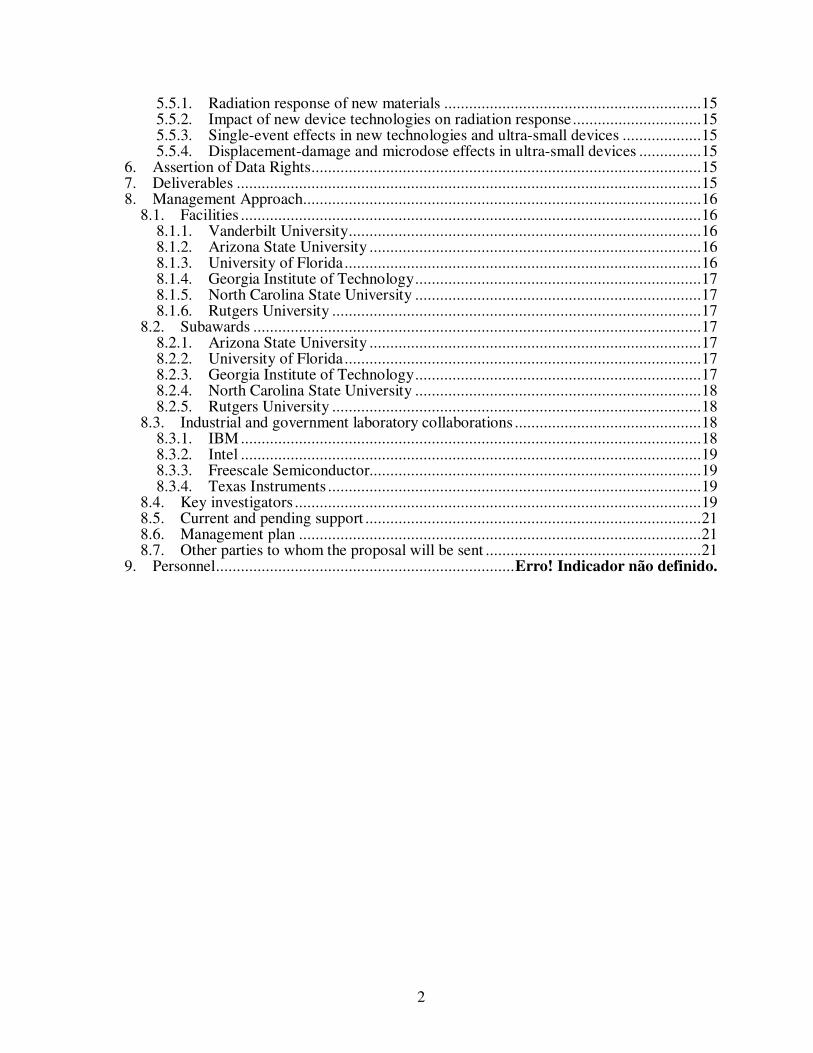
5.5.1. Radiation response of new materials ..............................................................15 5.5.2. Impact of new device technologies on radiation response...............................15 5.5.3. Single-event effects in new technologies and ultra-small devices ...................15 5.5.4. Displacement-damage and microdose effects in ultra-small devices ...............15
6. Assertion of Data Rights..............................................................................................15 7. Deliverables ................................................................................................................15 8. Management Approach................................................................................................16
8.1. Facilities ...............................................................................................................16 8.1.1. Vanderbilt University.....................................................................................16 8.1.2. Arizona State University ................................................................................16 8.1.3. University of Florida......................................................................................16 8.1.4. Georgia Institute of Technology.....................................................................17 8.1.5. North Carolina State University .....................................................................17 8.1.6. Rutgers University .........................................................................................17
8.2. Subawards ............................................................................................................17 8.2.1. Arizona State University ................................................................................17 8.2.2. University of Florida......................................................................................17 8.2.3. Georgia Institute of Technology.....................................................................17 8.2.4. North Carolina State University .....................................................................18 8.2.5. Rutgers University .........................................................................................18
8.3. Industrial and government laboratory collaborations .............................................18 8.3.1. IBM ...............................................................................................................18 8.3.2. Intel ...............................................................................................................19 8.3.3. Freescale Semiconductor................................................................................19 8.3.4. Texas Instruments ..........................................................................................19
8.4. Key investigators ..................................................................................................19 8.5. Current and pending support .................................................................................21 8.6. Management plan .................................................................................................21 8.7. Other parties to whom the proposal will be sent ....................................................21
9. Personnel........................................................................Erro! Indicador não definido.
3
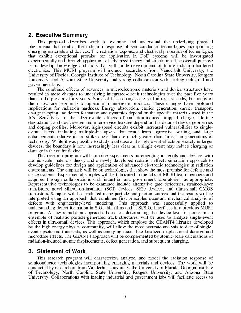
2. Executive Summary This proposal describes work to examine and understand the underlying physical
phenomena that control the radiation response of semiconductor technologies incorporating emerging materials and devices. The radiation response and electrical properties of technologies that exhibit exceptional promise for application in DoD systems will be investigated experimentally and through application of advanced theory and simulation. The overall purpose is to develop knowledge and tools that will guide development of future radiation-hardened electronics. This MURI program will include researchers from Vanderbilt University, the University of Florida, Georgia Institute of Technology, North Carolina State University, Rutgers University, and Arizona State University and strong collaboration with leading industrial and government labs.
The combined effects of advances in microelectronic materials and device structures have resulted in more changes to underlying integrated-circuit technologies over the past five years than in the previous forty years. Some of these changes are still in research labs, but many of them now are beginning to appear in mainstream products. These changes have profound implications for radiation hardness. Energy absorption, carrier generation, carrier transport, charge trapping and defect formation and dynamics depend on the specific materials used in the ICs. Sensitivity to the electrostatic effects of radiation-induced trapped charge, lifetime degradation, and device-edge and inter-device leakage depend on the detailed device geometries and doping profiles. Moreover, high-speed circuits exhibit increased vulnerabilities to single-event effects, including multiple-bit upsets that result from aggressive scaling, and large enhancements relative to ion-strike angle that are much greater than for earlier generations of technology. While it was possible to study total dose and single event effects separately in larger devices, the boundary is now increasingly less clear as a single event may induce charging or damage in the entire device.
This research program will combine experiments on emerging materials and devices with atomic-scale materials theory and a newly developed radiation-effects simulation approach to develop guidelines for design and application of advanced electronic technologies in radiation environments. The emphasis will be on technologies that show the most promise for defense and space systems. Experimental samples will be fabricated in the labs of MURI team members and acquired through collaborations with industrial and government laboratories, as appropriate. Representative technologies to be examined include alternative gate dielectrics, strained-layer transistors, novel silicon-on-insulator (SOI) devices, SiGe devices, and ultra-small CMOS transistors. Samples will be irradiated using particle and photon sources and the results will be interpreted using an approach that combines first-principles quantum mechanical analysis of defects with engineering-level modeling. This approach was successfully applied to understanding defect formation in SiO2 thin films and at Si/SiO2 interfaces in a previous MURI program. A new simulation approach, based on determining the device-level response to an ensemble of realistic particle-generated track structures, will be used to analyze single-event effects in ultra-small devices. This approach, which employs the GEANT4 libraries developed by the high energy physics community, will allow the most accurate analysis to date of single-event upsets and transients, as well as emerging issues like localized displacement damage and microdose effects. The GEANT4 approach will be complemented by atomic-scale calculations of radiation-induced atomic displacements, defect generation, and subsequent charging.
3. Statement of Work This research program will characterize, analyze, and model the radiation response of
semiconductor technologies incorporating emerging materials and devices. The work will be conducted by researchers from Vanderbilt University, the University of Florida, Georgia Institute of Technology, North Carolina State University, Rutgers University, and Arizona State University. Collaborations with leading industrial and government labs will facilitate access to
4
the most advanced technologies currently in development. The work is organized into four major tasks:
This MURI program will be organized into four principal tasks: 1. Radiation response of new materials 2. Impact of new device technologies on radiation response 3. Single-event effects in new technologies and ultra-small devices 4. Displacement-damage and total-dose effects in ultra-small devices.
The specific work to be undertaken includes: • Fabrication and radiation characterization of alternative gate dielectrics, including silicon
oxynitrides, HfO2, and related silicate films. • Analysis of radiation effects in devices fabricated on engineered substrates, including silicon
on insulator, strained Si, SiGe, and Si with various crystallographic orientations. • Use of first-principles quantum-mechanical calculations to understand the role of hydrogen
in determining the radiation response of emerging materials. • Quantification of the impact of new metallization and passivation systems on the energy
deposited by radiation in underlying circuitry. • Characterization and modeling of total-dose, single-event, and displacement-damage effects
in SiGe HBTs and SiGe-based BiCMOS technologies. • Characterization and modeling of total-dose and single-event effects in ultra-small
MOSFETs and MOSFETs with novel geometries, including, for example, FINFETs. • Refinement and application of a newly developed approach for simulating single-event
effects based on accurate modeling of a large number of realistic individual events. • Simulation and experimental validation of single-event effects in advanced technologies,
including SiGe HBTs, SOI and ultra-small MOSFETs, and optical data links. • First-principles calculations of mobilities in model nano-scale MOSFETs, including
scattering from radiation-induced defects • Simulation and validation of microdose and localized displacement damage (displacement
single events) in ultra-small devices. • Linkage of energy deposition simulations to first-principles atomic-scale calculations of
electrically active defects in irradiated semiconductors. The results of this work will be submitted for publication in appropriate refereed journals,
including IEEE Transactions on Nuclear Science, IEEE Transactions on Electron Devices, Physical Review Letters, Applied Physics Letters, Journal of Applied Physics, etc. Team members will present results at relevant technical conferences, including the IEEE Nuclear and Space Radiation Effects Conference and the International Electron Devices Meeting.
Each year of the program, Vanderbilt University will host an annual review that will be open to DoD attendees and external guests invited in consultation with the program manager. Annual reports and a final report will be provided.
4. Technical Approach
4.1. Background and approach
The goal of this work is to understand the radiation response of emerging electronic materials and devices through a combination of experimental, theoretical, and modeling methods. Approaches ranging from atomic-scale descriptions of defect formation to device-level analysis of transient effects will be employed. To examine radiation effects in highly scaled devices and new geometries, we will combine experiments, first-principles quantum mechanical calculations, and a new simulation approach based on detailed descriptions of individual radiation events. The impact of ultra-small geometries and new device structures will be considered, with emphasis on those aspects of emerging technologies that differentiate them from older technologies in which radiation effects are relatively well-understood. Radiation-induced defects that affect the electrical properties of new materials, devices, and the critical Si-
5
dielectric interface will be studied using sensitive electrical and physical characterization techniques and state-of-the-art theoretical methods.
4.1.1. Radiation effects
Long-term effects. Exposure to radiation produces relatively stable, long-term changes in device and circuit characteristics that may result in parametric degradation or functional failure. The total ionizing dose primarily impacts insulating layers, which may trap charge or exhibit interfacial changes. Non-ionizing energy loss results in displacement damage and defects in both insulator and semiconductor regions. In older technologies, these effects were well-described by a spatially uniform representation of the cumulative amount of energy deposited. The accuracy of this description relies on the relatively large size of the devices to average the energy deposited by individual particles or photons; in nano-scale devices, this approach is no longer valid.
Oxide trapped charge (Not) refers to radiation-induced charges, typically net positive, that are relatively stable. In ultrathin, high quality gate oxides, effects of oxide-trapped charge are minimal because of the small volume in which charge is generated and the ease with which it can tunnel from the oxide. However, high-κ dielectrics are currently more susceptible to ionizing radiation than thermal oxides of comparable effective thickness. In state-of-the-art MOS integrated circuits, field oxides and isolation structures are usually less radiation-tolerant than the active device regions. Ionizing radiation also results in formation of interface traps (Nit) at semiconductor/insulator boundaries that are able to exchange charge with the semiconductor on relatively short time scales. In MOSFETs, interface traps stretch out the subthreshold I-V characteristics and reduce the inversion-layer mobility. In BJTs, the current gain decreases with total dose due to increased surface recombination caused by interface-trap formation. Border traps are defects that are similar to oxide traps in microstructure but behave like slow interface traps, electrically.
The non-ionizing energy deposited by particle irradiation displaces atoms and creates electrically active defects. These defects reduce carrier lifetimes and mobilities, change carrier densities, and increase non-radiative transitions in optical devices, among other effects. Minority-carrier devices are particularly susceptible to displacement damage.
Transient effects. While the total-dose hardness of commercial integrated circuits has generally improved in recent years, primarily because of reductions in gate oxide thicknesses and increases in doping densities, reduced device dimensions and accompanying technological changes have resulted in increased sensitivity to transient radiation effects. Transient effects can be caused by individual ionizing particles (single-event effects) or high dose-rate ionizing radiation (
&γ radiation).
Single-event effects (SEE) are a serious problem for electronics operated in space and they are becoming an issue for advanced technologies in avionics, and even at sea level. The charge deposited by a single ionizing particle can produce a wide range of effects, including single-event upset, single-event transients, single-event functional interrupt, single-event latchup, single-event dielectric rupture, and others. In general, the sensitivity of a technology to SEE increases as device dimensions decrease and as circuit speed increases. These effects can be produced by direct ionization or by secondary particles resulting from nuclear reactions or elastic collisions. Recent experimental results from heavy ion and proton irradiations of advanced devices have demonstrated unpredictable SEE responses.
In a high dose-rate environment, energy is generated relatively uniformly throughout the integrated circuit. The resulting photocurrents produce effects that include rail-span collapse, cell upset, and burnout of metal lines. Depending on system requirements, it may be necessary to operate through a dose-rate event or it may be possible to circumvent it by temporarily removing power.
4.1.2. Impact of new materials and structures
Every aspect of semiconductor technology, ranging from substrates to metallization, is undergoing changes in response to continued demands for increased integrated-circuit
6
complexity, higher performance, and lower cost. Some of the most significant changes in materials and structures that have the potential to affect radiation response are listed here.
(1) Gate stacks. High-κ dielectrics provide the same capacitance per unit area as SiO2 but allow thicker films to be used. Metal and fully silicided (FUSI) gates eliminate the poly-depletion effect, increase conductivity, and improve speed.
(2) Interconnect technology. The combination of multi-layer, planar copper metallization with low-κ interlayer dielectrics helps to solve the problems of on-chip delays, power distribution, and signal routing.
(3) Packaging and passivation. New materials have been deployed as passivation layers and in packaging. These materials have the potential to affect the radiation-deposited energy in underlying devices.
(4) Substrate engineering. Carrier mobility can be significantly boosted by substrate engineering, including strained silicon with SiGe buffer layers, strain induced by device structures, and substrate orientation effects. Various forms of silicon-on-insulator (SOI) MOSFETs now are employed in advanced technologies from several manufacturers. More advanced device substrates, such as SGOI, GOI, bulk Ge, and SSOI are under intense investigation.
(5) Device structures. Double-gate, Π-gate, tri-gate, Fin-FET, and gate-all-around MOSFETs increase transconductance and reduce subthreshold swing. Lateral double-diffused MOS (LDMOS) devices provide integrated RF and high-voltage capability. SiGe HBT BiCMOS technology has made it possible to integrate an entire radio on a single chip.
The above changes in materials and structures present new challenges for understanding radiation effects and developing radiation-tolerant devices and structures. The challenges range over several length scales, from the quantum world of electrons and nuclei to the macroscopic distribution of energy deposited in the entire device; from the effects of atomic-scale radiation-induced point-defect dynamics on mobilities, carrier trapping and detrapping to current-voltage characteristics and circuit performance. These issues must be addressed in a coordinated way that integrates experimental and theoretical results across length scales.
4.2. Technical organization
This MURI program will be organized into four principal tasks: 1. Radiation response of new materials 2. Impact of new device technologies on radiation response 3. Single-event effects in new technologies and ultra-small devices 4. Displacement-damage and total-dose effects in ultra-small devices.
Each of these technical areas is described in detail in the following sections.
4.3. Radiation response of new materials
4.3.1. Background
Low power applications of CMOS circuits, such as those envisioned for future defense and space systems, require leakage current limits of ~10-4-10-2 A/cm2, defining a minimum EOT (effective oxide thickness of SiO2) of 1.8 to 2.5 nm, and a decrease in EOT for optimized Si oxynitride devices by about 0.2 to at most 0.3 nm. This limitation establishes a need for high-κ alternative gate dielectrics. Replacement of polysilicon gate electrodes by metal gate electrodes offers more scaling potential due to poly-depletion elimination. Additional performance improvements are being made in industry by channel engineering, i.e., by using strained Si and/or SiGe alloys to improve channel transport properties,
Materials to be examined in this program can be classified into several broad categories: • first-generation (HfO2-based) and emerging high-κ dielectrics and stacks with engineered
interfaces that reduce defects through processing or compositional control, for example by either nano-scale self-organizations and/or balancing bonding and force constant constraints
7
• dielectric/semiconductor interfacial layers (e.g., SiO2, SiON, and SiNx) with thickness and composition chosen to balance interfacial strain and passivate the Si substrate against chemical reaction with high-κ metal atoms.
• metal gate electrodes and their interfaces with high-κ dielectrics that mark the transition from poly-Si to metal, metal nitride, or silicide.
• substrate materials including Si, strained Si, Si orientations (i.e., (100), (111), (110)), SiGe, and Ge, as well as structured substrates such as SOI and three-dimensional FIN/FAN structures that allow multiple gates. In addition to the active device regions, a wide variety of new materials have been
incorporated in the back-end of semiconductor processes (metallization, interlayer dielectrics, and passivation). The primary impact of these materials on radiation response is their effect on the energy deposited in the underlying circuitry. These effects are described in Sections 4.4.3 and 4.5.
The PIs of this program and their collaborators use a very broad range of growth, characterization, and spectroscopy tools, complemented by theory and modeling. The experimental methods are briefly summarized here. Growth: Plasma and conventional CVD, ALD, reactive PVD and MBE. Electrical: CV, IV, mobility, low frequency noise, charge pumping, constant voltage stress, thermally stimulated current, EPR and other techniques. Structural: Atomic-resolution Z-contrast STEM and EELS, TEM/SEM, scanning probe topography and spectroscopy. Composition: SIMS/RBS/MEIS/XPS. Advanced Spectroscopy: XAS, optical second harmonic generation, cathodoluminescence spectroscopy, photoemission.
4.3.2. Proposed Research—Gate Stacks
The proposed program will emphasize the first generation of alternative dielectrics, viz. HfO2-based materials including nitrided HfO2 and Hf silicates that have emerged from academic and industrial research as leading candidates for implementation in CMOS in the next 5-year time frame. Equally important, the proposed program will anticipate second generation, atomically engineered stacked dielectrics and other high-κ materials options that have been identified in advanced research tasks in SRC and SRC/ISMT-sponsored programs. A critical aspect of this forward-looking direction is the combination of device testing, in the context of stress bias (current) testing with total dose radiation testing, with studies of electronic structure (band offsets, localized states, etc.) by advanced spectroscopy and theory in order to understand the radiation sensitivity at the atomic level. Both current industry-standard HfO2-based dielectrics and emerging new materials and structures will be evaluated to determine response with respect to single-event, displacement-damage, and total-dose effects. Details of both gate stack structure (including an important aspect of interfaces) and their fabrication technology may have a strong influence on the final materials ensemble and hence on the sensitivity, and these will be addressed as well. The program will carefully monitor and measure the materials configuration using physical probes listed above. Radiation sensitivity will also be monitored with sensitive electrical, electronic, and optical means, and complemented by theory and modeling at the atomic scale.
The program will address the following issues: (1) Stress biasing and radiation testing of alternate dielectrics with conventional poly-Si and advanced metal gates (including novel fully silicided gates); (2) Atomic scale understanding and control of radiation induced processes in advanced materials, such as defect generation; (3) Role of H and deuterium in radiation effects in alternate dielectrics; (4) Radiation hardened gate stacks by interface engineering and composition control; and (5) Alternate dielectrics on engineered substrates, e.g., strained Si and Ge.
The extensive parameter space makes it essential for the judicious selection of materials and structures with a balance between the first generation HfO2-based materials and dielectrics emerging from SRC and SRC/SEMATECH programs. The major emphasis will be on the current industry standard materials, and a smaller effort, leveraged heavily by other government and industrial support, will address the emerging new materials and structures.
8
The general outline of the work will be as follows: materials growth/formation and test device fabrication (IBM, Rutgers, Sandia, NCSU); materials and interface characterization, spectroscopy and theory (Rutgers, Vanderbilt, IBM, NCSU); evaluation of electrical properties (w/wo radiation) (Vanderbilt, IBM, NCSU). The overall objectives are two-fold: to define devices that meet DoD needs in future defense and space systems, and build a firm foundation that couples atomic structure, chemical bonding, and electronic structure, with an atomic scale understanding of defect generation and relaxation that draws on both electrical and radiation testing.
4.3.3. Role of hydrogen
Much of radiation-induced defect generation is mediated by hydrogen that is initially trapped at defects, impurities, and interfaces. Radiation-induced holes enhance the release of H, typically as H+, which then migrates and causes defect-generating reactions. In the last five years, several of the current PIs engaged in a systematic study of the consequences of radiation-induced H release in MOSFETs. Using density functional theory (DFT) calculations and available experimental data, the atomic-scale mechanisms of several important radiation-effects phenomena were elucidated. For example, large fluxes of holes arriving at the interface during high-dose-rate irradiation are trapped at border O vacancies where they form an electrostatic fence, keeping large fluxes of H+ from arriving at the interface. This effect suppresses the formation of interface traps at high dose rates and leads to the enhanced low-dose-rate sensitivity (ELDRS) of BJTs. In another example, it was shown that H+ arriving at the interface easily migrates laterally and depassivates dangling bonds (DBs) directly, without the need to convert to neutral H as assumed by earlier work (SiH+H+
→DB++H2). This lateral-transport mechanism determines the apparent activation energy of several forms of radiation-induced degradation. The above atomic-scale reactions (plus other related reactions) were modeled by diffusion-reaction equations and by Monte-Carlo methods, providing direct modeling of experimental data. The atomic-scale mechanisms were then incorporated in higher-level engineering device models.
We will pursue corresponding calculations for similar phenomena in MOSFETs with alternative dielectrics, strained-Si channels, and novel SOI-based structures. Differences from the phenomena in standard MOSFETs will be identified. In particular, we will develop models of nitrided Si-SiO2 interfaces and study the behavior of H in such systems. We will also study the behavior of H in novel dielectrics that have a thin SiO2 layer followed by HfO2 or other metal oxides. In all cases, the behavior of H in equilibrium and under radiation conditions will be elucidated and the atomic-scale results will be incorporated in engineering models.
4.3.4. Substrate engineering
Substrate engineering is an important new direction to improve performance of sub-100 nm devices. Modern devices increasingly use strain to alter the band structure and mobility through nanoscale engineering with Si/SiGe layers for both FETs and bipolar devices (SiGe HBT). The responses of these devices to radiation are not yet understood. The high speed of emerging Si-based strained-layer devices makes them highly susceptible to single-event upsets and transients. Studies of the impact of radiation on the inherent thermodynamic stability of the requisite Si/SiGe nanoscale films required for devices will be conducted, and the fundamental radiation-induced defects probed and compared to those known in the Si material system. We will examine these effects using experiments, first-principles calculations, and simulation. Most device simulators take strain into account by simply altering the inversion-layer mobility (for FETs) or bandgap (HBTs), and assuming a uniform strain distribution. While this may be sufficient for first-order simulation of DC and AC device characteristics, it is not adequate for describing radiation events in which charge densities are very high and distributed throughout the active device volume. Implementing spatially dependent, strain-induced band structure and mobility changes, coupled with the microstructure of radiation events, is required for modeling the charge transport and collection due to single events.
We have developed a method for calculating mobilities using first-principles quantum mechanical methods that go beyond the effective mass approximation and can include strain by
9
simply using a suitably larger lattice constant. The method allows for wave function penetration in the gate dielectric, incorporates atomic-scale interface roughness, and can explicitly include scattering from radiation-induced defects (see Section 4.4.1 for details). Results obtained from these calculations will be incorporated into existing device modeling programs.
4.4. Impact of new device technologies on radiation response
This task will focus on understanding the implications of three emerging trends in device technology on radiation response: ultra-small MOSFETs, SiGe HBTs, and new metallization and passivation systems.
4.4.1. Ultra-small MOSFETs
Highly scaled CMOS microelectronics will be the first nanotechnologies used in space and defense systems. Notable changes include the use of SOI (for increased performance per unit of power dissipation, and enhanced soft-error immunity), non-planar device geometries, and strained layers (for improved mobility). SOI also makes it possible to use new device structures, including gate-all-around structures, and most recently, a “Π-Gate” structure that is compatible with nanoscale CMOS device fabrication and exhibits excellent radiation tolerance. Moreover, alternative dielectrics are required to avoid excessive tunnel currents through thin gate dielectrics. The radiation response and reliability of dielectrics other than SiO2 are not well understood, and are likely to differ significantly from the well-known responses of present MOS gate dielectrics and isolation layers. The combined effects of these changes will significantly affect the radiation response.
The total-dose and single-event response of very deep submicron CMOS technologies will be evaluated using integrated circuits and test structures acquired from our industrial and government partners (described below). Total ionizing dose (TID) testing will be conducted at Vanderbilt and ASU using x-ray and γ-ray sources; measurements will include I-V, C-V, transconductance, leakage current, and 1/f noise. The results of total dose testing will be interpreted using physical and device modeling techniques to determine the impact of device design, (e.g., geometry, doping, etc.) on TID susceptibility. The results of single-event testing (threshold LET, saturated cross-section, SET pulse width, proton sensitivity, etc.) will be compared to novel simulations based on large numbers of physically-realistic particle tracks determined by a GEANT4-based code developed at Vanderbilt (described in Section 4.5).
Mobilities in strained-Si channels and ultrathin SOI-based single-gate and double-gate MOSFETs than those in standard MOSFETs. Simulations of mobilities in the usual approximations (infinite barrier at the Si-SiO2 interface, phenomenological interface roughness, model scattering mechanisms, and in most cases, the effective mass approximation) have not been able to account for the effects. We have developed a method to calculate mobilities in nano-scale single- and double-gate devices based on DFT electronic structure calculations. We start with a reference structure containing abrupt interfaces and then introduce atomic-scale roughness (suboxide bonds or Si-O-Si protrusions) or other point defects, including radiation-induced defects. The difference in electrostatic potentials then serves as the scattering potential for the calculation of mobilities. These calculations will incorporate the penetration of the wave functions of electrons into the gate dielectric, an effect that is particularly important for alternative dielectrics with small energy-band offsets. Mobilities will be calculated at various levels of approximation, compared with experimental results, and incorporated in compact models for circuit modeling.
4.4.2. SiGe HBTs
In SiGe technology, a small amount of Ge is introduced into the base of a Si bipolar transis-tor, increasing operating speeds by a factor of 2-3 over comparable Si devices, while at the same time reducing power consumption significantly. SiGe’s fabrication compatibility with conventional Si CMOS processing ensures that both high-speed SiGe HBTs and aggressively scaled CMOS devices can be co-integrated on the same Si wafer, making it possible to combine analog, RF/microwave, and digital functions on a single chip. The technology is functional, with
10
low noise, to cryogenic temperatures, making SiGe particularly suitable for readout circuitry in infrared sensors.
Recent work from MURI team members has shown that as-fabricated, commercial SiGe HBTs and SiGe HBT BiCMOS technologies are radiation-hard up to at least 5 Mrad(SiO2), and highly resistant to proton and neutron-induced displacement damage. The ability to produce a Si-based IC technology that delivers III-V device performance at Si cost is potentially revolutionary for high-performance, low-cost defense and space systems. Professors Cressler and Reed have been involved in a multi-year research project, funded by DTRA and NASA, focused on examining radiation effects in IBM’s SiGe BiCMOS processes [1, 2, 3, for example]. However, experiments have demonstrated the need to understand and improve the SEE response of SiGe HBT and BiCMOS technologies and also to investigate the impact of radiation on profile stability and defects in the requisite SiGe strained layers used in the technology. In this program, we will characterize and model four unique generations of IBM's state-of-the-art SiGe technology, considering TID, SEE, and displacement damage. IBM has agreed to fabricate circuits and test structures designed by team members and provide access to doping profiles, device layouts, etc. that are required for calibration of 2D/3D simulations. DTRA’s Radiation Hardened Microelectronics Program and the NASA Electronic Parts and Packaging Program have agreed to collaborate with the research team to provide test capabilities and support.
4.4.3. Metallization and passivation systems
Advanced ICs have complex material systems covering the active device layer that may affect the radiation response. Most modern technologies use multiple layers of planarized interconnects, typically fabricated using a dual-damascene copper process. Additional materials, including low-κ dielectrics, barrier metals, and metal vias are also part of the metallization system. The passivation layers that cover the metallization also may absorb incoming radiation and affect the energy deposited in the underlying layers. These changes in back-end technology may have significant impacts on the radiation response in several ways: (1) materials, particularly metals such as W, may interact with incoming particles to produce showers of secondary particles that produce single-event effects in underlying devices, (2) due to the presence of multiple materials, dose-enhancement effects may occur in the lower-Z materials, and (3) the sensitivity to dose-rate related phenomena such as rail-span collapse or burnout of metal lines may be different for these systems. The simulation approach described in Section 4.5 will be used to calculate the effects of overlayers, taking into account realistic material properties and layer thicknesses. The transient currents produced at the device level will be determined from 3D simulations and compared to experimental data.
4.5. Single-event effects in new technologies and ultra-small devices
4.5.1. Limitations of existing models
While classical test methods and SEE rate-prediction methods are very robust and estimate the observed SEE rates of most current devices accurately (see for example [4]), these methods have limitations that become more serious as device dimensions decrease. Several effects have been identified in recent technology generations that result in significant inaccuracies in SEE rate predictions, demonstrating the importance of developing new modeling and analysis capabilities for emerging technologies. These effects include failure of the effective LET concept [5], ion track structure effects [6],[7], SEE in SiGe HBTs, SETs in optocouplers and optical data links [8], [9], [10], [11], and charge collection resulting from charge deposited below the buried oxide in SOI technologies that have very thin buried oxide layers [12].
4.5.2. Proposed Work
We will extend and apply a fundamentally new radiation-effects simulation strategy that is based on detailed analysis of the microstructure of individual radiation events to understand single-event effects in digital, analog and mixed-signal circuits employing sub 100-nm devices. Until very recently, the interaction of radiation with devices has been quantified by the average
11
deposited energy along a particle track (e.g., LET or non-ionizing energy loss (NIEL)). The validity of this approach relies on the large size of the device to integrate the effects of the radiation, which is no longer the case in highly scaled devices. By describing radiation environments using a large number of events initiated by individual primary radiation quanta and studying device response to these individual events, we will obtain both average device response and statistical variability. This will allow us to analyze quantitatively processes such as multiple bit upsets, secondary radiation from materials near active devices, microdose, and highly localized displacement damage, which depend on the microstructure of radiation interactions with emerging devices.
The interaction of the radiation with the materials and devices will be analyzed using Vanderbilt-customized tools based on Geant4 (a comprehensive library of C++ routines) and flexible 3D simulation tools developed at the University of Florida. FLOODS (FLorida Object Oriented Device Simulator) includes a scripting language for partial differential equations, which makes it straightforward to add models and adapt them for advanced devices. ASU will use the results as inputs for IC-level analysis.
The simulations conducted as part of this task will support all of the other program tasks, e.g., they will be used to analyze problems ranging from the effects of novel device geometries, like Π-gate MOSFETs, on single-event response to effects of overlayers on energy deposition in sensitive device volumes. Validation and verification will be performed using test structures and devices provided by industrial partners. In addition, the simulations will be used to look at the single-event response of future generations of technologies. This type of “look-ahead” analysis is made possible by the physically rigorous approach of the simulation methodology.
4.6. Displacement-damage and microdose effects in ultra-small devices
4.6.1. Background
In conventional-size devices, the radiation response to single events is distinct from that due to total dose irradiation or displacement damage. In single events, only transient phenomena related to ionization are considered because the displacement damage along the particle path plus the charging in that vicinity are too localized to produce significant effects in conventional devices. Thus displacement-damage and total-dose effects are considered to be averaged effects, described by volumetric or areal defect concentrations. However, in ultrasmall devices, a single event may result in both displacement damage and significant increases in trapped charge and interface defects. Related effects have been observed in larger technologies, and the effects will be much more serious as device dimensions move well below 100 nm [13]. Electrical effects may include locally-large threshold-voltage shifts, dramatically decreased mobility, and high recombination in damaged areas.
Today, the generally accepted measure of displacement damage by ion irradiation is the nonionizing energy loss (NIEL), a beam property measuring energy surrendered per unit of path length to whole-atom motion in the solid. It has been assumed that the concentration of electrically active defects is simply proportional to this quantity. However, data exist in GaAs that call this assumption into question [14]. The crucial issue is to establish the quantitative relationship between the density of deposited energy and resulting density of electrically active defects.
4.6.2. Proposed Work
The key issue in this work is to bridge the energy and length scales so that Geant4, with its essentially complete collision physics, can be used to quantify energy deposition, while density functional theory, with its own first-principles physics, is used to establish final conditions. Geant4 simulations will be used to establish statistical information on the distribution and initial energy of collision cascades in selected materials. This information will be used to establish, by comparison with data, target cases where computation can shed light on fundamental mechanisms. The intermediate stage of the process may involve regions of a million or more atoms. We will use an approximate version of DFT in which the electron density is modeled by
12
spherical “atomic” densities, where the latter are determined by a variational principle. There are no wave functions. The method has been developed and tested and shown to be a practical DFT-derived alternative to “classical potentials”. We will test the method for energetic particles. We anticipate that we will be able to simulate at least thousands of atoms and further develop algorithms for hundreds of thousands of atoms to simulate microdose and displacement single events in restricted regions.
To model the very late stages of collision cascade evolution, where electrically active defects are presumably frozen into the system, we will use full density functional theory on appropriately restricted systems, taken from an analysis of the DFT molecular dynamic simulations described above. We will use time-dependent DFT to simulate the evolution of both electrons and nuclei under the total quantum mechanical forces. The central issue will be to compare the resulting configuration and electrical activity of various configurations as a function of the initial energy of cascades, particularly those resulting from direct beam-target interactions and others from the interactions of heavy recoils following nuclear reactions. This analysis will be extended to the much more complex events produced by heavy nuclear recoils.
At the engineering-model level, FLOOPS has defect models based on implantation damage. These models focus on the initial amount of damage and subsequent annealing. Point defects are mobile in silicon at very low temperatures and can travel long distances by device standards. We will fully model the generation events, the defect transport, and the eventual relaxation into stable clusters. The models that result from the DFT calculations will be incorporated into FLOOPS for simulation of device response over longer times.
4.7. Impact on DoD Systems
Future DoD systems must be able to use the most advanced electronics available to assure U.S. technical superiority. However, recent changes in the materials and devices used in integrated circuits make it necessary to assess the reliability and survivability of advanced technologies in radiation environments. This MURI program will develop tools and methods for analyzing the radiation response of emerging technologies and evaluate candidate materials and devices. This will speed insertion of the most advanced technologies into DoD systems, contribute to the development of electronics with improved radiation survivability, and provide improved radiation-hardness assurance capabilities for future systems.
The results of this MURI program will impact all future DoD programs that require radiation-hardened electronics. As new systems are designed and existing systems go through life-extension programs, designers and program managers will be able to draw upon the information about radiation-tolerance of advanced technologies. Engineers involved in risk assessment will benefit from the simulation and analysis methods that will be developed. Suppliers of radiation-hardened microelectronics will be able to apply the results to improve the hardness of their future technologies. Finally, this work will provide a firm foundation for future applied research and development activities in radiation-hardened microelectronics.
4.8. Student training
This research program will emphasize education and training of graduate students as a core part of its mission. The shortage of trained radiation-effects specialists has been identified as a critical need by the DoD and the problem is becoming worse as many of the long-time practitioners in the field reach retirement age. Vanderbilt has one of the only graduate programs in the U.S. emphasizing radiation effects in electronics and it has the only academic research institute actively involved in supporting the DoD’s requirements for strategically hardened parts. In addition, graduate students have the opportunity to gain experience in modeling at all length scales, from atomic-scale quantum mechanical calculations to engineering models (such students have already graduated from the program).
Each year, undergraduate students will be invited to participate in MURI-related research as part of Vanderbilt’s summer research program for undergraduates. The most promising students will be encouraged to continue their research during the academic year with the goal of recruiting them as MURI-sponsored graduate students. Vanderbilt’s Radiation Effects and
13
Reliability Group has successfully used this approach to recruit outstanding graduate students for previous research programs, including an AFOSR-sponsored MURI program.
The estimated number of graduate and undergraduate students who will participate in the MURI program each year is outlined in Volume 2 of this proposal.
5. Project Schedule and Milestones
5.1. Year 1
5.1.1. Radiation response of new materials
• Emphasis on HfO2-based dielectrics with a smaller effort on novel emerging high-κ materials. Test devices for stress-bias and rad testing to include poly-Si and selected metal gates. Role of interface engineering (its thickness and composition).
• Theory: i) Damage sensitivity via GEANT4; ii) nitrogen and hydrogen in SiON interfaces
5.1.2. Impact of new device technologies on radiation response
• First-generation SiGe devices: DLTS and XRD SiGe stability experiments before and after irradiation (total dose and displacement) – theory of defects
• 2D/3D modeling of TID defect buildup and response in scaled SOI CMOS technologies; 3D model development for SiGe devices
5.1.3. Single-event effects in new technologies and ultra-small devices
• Develop energy deposition models for SiGe and other material systems; complete density gradient models for charge quantization in inversion layers
• Validate Geant4 nuclear reaction fragmentation pattern predictions • Quantify effects of passivation and metallization layers on energy deposition and statistics • DFT calculations of mobilities and radiation response in nanoscale MOSFETS
5.1.4. Displacement-damage and microdose effects in ultra-small devices
• Develop 3-D displacement damage energy deposition maps in SiGe HBTs and other devices • 2D/3D modeling of DD and micro dose effects in SOI CMOS and SiGe HBT technologies
5.2. Year 2
5.2.1. Radiation response of new materials
• Systematic studies of metal gated HfO2-based dielectrics, and test device studies on emerging materials. Effect of processing, viz. deposition technique and annealing, on rad. response.
• Theory: (i) Comparison to GEANT4 for different layered structures; (ii) H diffusivity in defected/nondefected layers and H stability/reactivity at the interface (DFT)
5.2.2. Impact of new device technologies on radiation response
• Design and fabricate SiGe HBT test structures and digital circuits (e.g., shift registers) for TID, SEE, and microbeam studies for simulation to data calibration
• DLTS and refined XRD SiGe stability experiments in second-generation SiGe devices before and after irradiation
• TID model validation for SOI CMOS and SiGe HBT technologies
5.2.3. Single-event effects in new technologies and ultra-small devices
• Completion of surface scattering models for inversion layer mobility; strain simulations on DC test cases; full piezoresistance models
• Coupling to charge distribution from GEANT, first transient simulations; validate Geant4 models of diodes using commercial and FLOODS simulators; mobility calculations
14
5.2.4. Displacement-damage and microdose effects in ultra-small devices
• Link device-level energy deposition to DFT molecular dynamical simulations • Experimentally measure localized displacement in highly scaled CMOS and other devices
5.3. Year 3
5.3.1. Radiation response of new materials
• Measurements of hydrogen concentrations, hydrogen diffusivity, radiation enhanced diffusivity in alternate dielectrics, including engineered substrates. Exploratory studies of first generation devices on engineered substrates, strained Si, Si orientations, Si/SiGe and SOI.
• Theory: GEANT–rate of damage build up; DFT–defect geometry
5.3.2. Impact of new device technologies on radiation response
• Refined SiGe HBT test structures and digital circuits for TID, SEE, and microbeam studies for simulation calibration; fabricate test structures on SiGe films used in stability experiments; total dose and displacement experiments on third-generation SiGe HBTs; DLTS experiments of traps in third-generation SiGe devices before and after irradiation
• Revision of 2D/3D models of TID defect buildup and response in scaled SOI CMOS and SiGe HBT technologies
5.3.3. Single-event effects in new technologies and ultra-small devices
• Strain simulations coupled to charge removal simulations • Quantify energy deposition statistics in small device volumes; evaluate device performance
statistics in automated parallel ensemble simulations in various devices • 3D SiGe model development/interpretation
5.3.4. Displacement-damage and microdose effects in ultra-small devices
• Compute probabilities for multiple-device displacement events in ICs • Experiments on SiGe HBT (microdose and DD) and SOI CMOS (microdose) devices
5.4. Year 4
5.4.1. Radiation response of new materials
• Increased studies on devices, both first generation, and maturing novel devices on SOI, stained Si/SiGe, and including three-dimensional structure FINFET structures.
• Theory: Hydrogen in metals, diffusivity, solubility, grain boundary diffusion (DFT)
5.4.2. Impact of new device technologies on radiation response
• Refined SiGe HBT test structures for TID and microbeam studies for calibration; initial SiGe HBT mixed-signal circuits (e.g., amplifiers, oscillators, etc.) for SEE evaluation and comparison to simulation results
• DLTS experiments of traps in fourth-generation SiGe devices and test structures developed for stability profile study – theory of defects
• Experiments on SOI CMOS (TID) and fourth-generation SiGe HBTs (TID and DD)
5.4.3. Single-event effects in new technologies and ultra-small devices
• Full anisotropic modeling of mobility and bands from strain; implementation of energy balance models, coupling to energy deposition of carriers
• Apply ensemble TCAD simulation to ultra-small volume devices and systems
5.4.4. Displacement-damage and microdose effects in ultra-small devices
• Correlate computed displacement damage in dielectrics to leakage and rupture
15
• Revision of 2D/3D models of DD and microdose defect buildup and response in scaled SOI CMOS and SiGe HBT technologies
• Radiation experiments on SOI CMOS (microdose) and SiGe HBTs (microdose and DD)
5.5. Year 5
5.5.1. Radiation response of new materials
• Increased focus on test device fabrication, device measurements, and rad testing on bulk CMOS and novel device structures employing emerging materials. alternative dielectrics, channel engineering, metal gates, and structures, multiple gates, and FINFETs
5.5.2. Impact of new device technologies on radiation response
• Refined SiGe HBT test structures and mixed-signal circuits for TID, SEE, and microbeam studies for calibration; total dose and displacement) experiments on fifth-generation HBTs
• DLTS experiments on traps in fifth-generation SiGe devices and test structures developed for stability profile study before and after irradiation
• Refinement of models and technology extrapolation techniques for predicting TID defect buildup and response in scaled SOI CMOS and SiGe HBT technologies
5.5.3. Single-event effects in new technologies and ultra-small devices
• Coupling of anisotropy to energy balance • Evaluate and compare experimentally identified radiation effects anomalies in ultra-small
devices with highly-parallel and detailed-event simulations
5.5.4. Displacement-damage and microdose effects in ultra-small devices
• Apply energy deposition and density functional theory models to predict electrically active displacement damage in SiGe and highly scaled CMOS systems
• Refinement of models and technology extrapolation techniques for predicting DD and microdose defect buildup and response in scaled SOI CMOS and SiGe HBT technologies
6. Assertion of Data Rights None.
7. Deliverables The formal deliverables for this program will include annual progress reports and a final
technical report. The results of the research will be presented at appropriate technical conferences and submitted for publication in refereed journals. The specific subjects of the presentations and publications will include:
1. Fabrication and radiation characterization of alternative gate dielectrics, including silicon oxynitrides, HfO2, and related silicate films.
2. Analysis of radiation effects in devices fabricated on engineered substrates, including silicon on insulator, strained Si, SiGe, and Si with various crystallographic orientations.
3. Use of first-principles quantum mechanics calculations to understand the role of hydrogen in determining the radiation response of emerging materials.
4. Quantification of the impact of new metallization and passivation systems on the energy deposited by radiation in underlying circuitry.
5. Characterization and modeling of total-dose, single-event, and displacement-damage effects in SiGe HBTs and SiGe-based BiCMOS technologies.
6. Characterization and modeling of total-dose and single-event effects in ultra-small MOSFETs and MOSFETs with novel geometries, including, for example, FINFETs.
7. Refinement and application of a newly developed approach for simulating single-event effects based on accurate modeling of a large number of realistic individual events.
16
8. Simulation and experimental validation of single-event effects in advanced technologies, including SiGe HBTs, SOI and ultra-small MOSFETs, and optical data links.
9. First-principles calculations of mobilities with atomic-scale roughness, radiation-induced defects
10. Simulation and validation of microdose and localized displacement damage (displacement single events) in ultra-small devices.
11. Link energy deposition simulations to atomic-scale calculations of electrically active defects in irradiated semiconductors.
8. Management Approach
8.1. Facilities
8.1.1. Vanderbilt University
Vanderbilt has an extensive suite of test and characterization equipment for radiation-effects analysis, including an ARACOR 10-keV x-ray irradiator, two Cs-137 isotopic irradiators, and a 2-MeV proton source. Vanderbilt team members have extensive experience conducting single-event tests at facilities including Brookhaven National Laboratory, Michigan State University, and Indiana University. An array of test equipment is available to facilitate the characterization of irradiated devices and ICs. Vanderbilt also has in place a Cooperative Research and Development Agreement (CRADA) with NAVSEA-Crane that provides access to a suite of radiation sources and a fully equipped parts analysis laboratory. Vanderbilt’s Advanced Computing Center for Research and Education (ACCRE) houses VAMPIRE, a Beowulf cluster supercomputer used to execute Vanderbilt’s Technology Computer Aided Design (TCAD) suite and the particle interaction simulator based on Geant4. Currently the majority of the nodes (~200) are dual 2.0 GHz Xeon and Opteron processors. Expansion to 1200 processors by mid-2005 is underway.
8.1.2. Arizona State University
Arizona State University has three irradiators: Gammacell 200 and 220 Co-60 industrial irradiators, and a low dose rate Shepherd 1.2 Ci Cs-137 point source. Both Gamma Cells are equipped with temperature chambers. Facilities in ASU centers include a 30,000 sq. ft. C100 clean room equipped with oxidation and diffusion furnaces, aligners and high resolution lithography, RTA plasma etch, metal deposition, CVD tools and advanced imagers (SEM and FIB). ASU is also in the process of expanding to a 64-node Beowulf cluster for use in radiation effects simulation using Silvaco’s TCAD plus Radiation Effects Module (REM) suite.
8.1.3. University of Florida
The Advanced Computing and Information Systems (ACIS) laboratory is equipped with state-of-the-art computing, storage and networking facilities and has a unique environment that supports virtualization technology of commercial and open-source projects. The ACIS lab owns and operates the following computer systems which are connected to the University backbone through a gigabit network: a 64-CPU IBM xSeries 1350 cluster, a 12-CPU IBM eServer Cluster 1300, a 192-CPU IBM SP/2 cluster, an IBM ESS Total Storage Enterprise Server (IBM 2105-800 3.36 TB), and an IBM eServer 1.2TB SCSI/RAID disk array. Microfabrication equipment is housed in the UF NanoFab Facility (UFNF). Its capabilities include a Raith 150 e-beam lithography system, a Karl Suss Deep UV mask aligner, a Kurt J. Lesker Multi-Target Sputter Deposition System for metals and dielectrics, a Surface Tech System plasma-enhanced chemical vapor deposition system, a Unaxis Inductively-Coupled Plasma Etcher, a Surface Tech Systems Deep Reactive Ion Etcher/Bosch Process System, and a plasma asher for hard mask removal.
17
8.1.4. Georgia Institute of Technology
The High-Frequency Systems Laboratory at Georgia Tech has measurement capabilities for materials, devices, and circuits, ranging from dc to mm-wave (110 GHz), fA to A, and across the temperature range of 15K to 500C. The SiGe IC Design Laboratory contains 40 high-end Sun Design Systems, running all major simulation and modeling software packages. Cressler’s SiGe research team has substantial experience in SiGe HBT mixed-signal circuit design using the Cadence design environment, and has worked extensively with IBM’s SiGe IC design kits (5HP, 7HP, and 8HP). Device simulation and modeling makes use of TCAD tools from ISE and Synopsys. Comprehensive IC fabrication within the Microelectronic Research Center and packaging facilities within the NSF ERC Packaging Research Center are available to support this program.
8.1.5. North Carolina State University
NCSU has equipment for thin film deposition under ultra-high vacuum conditions, including remote plasma-enhanced chemical vapor deposition systems. Characterization facilities include infrared, Raman, X-ray photoelectron, and Auger electron spectroscopies. NCSU has advanced spectroscopic facilities including i) in-line AES, XPS and UPS, ii) vacuum UV spectroscopic ellipsometry, and iii) optical second harmonic generation. NCSU researchers also use facilities at national laboratories, including i) x-ray absorption spectroscopy at the NSLS at BNL and SSRL at SLAC, and ii) XPS at NSLS and SSRL.
8.1.6. Rutgers University
Rutgers has ultrahigh vacuum surface analysis systems with facilities for Auger, photoelectron (XPS & UPS), and electron energy loss (HREELS) spectroscopy, mass spectrometry, low energy electron diffraction (LEED), electron stimulated desorption ion angular distribution (ESDIAD) measurements, low energy ion scattering, and He atom scattering; scanning tunneling microscopes; and atomic force microscopes. Additional equipment includes a Smart APEX CCD single-crystal diffraction system, two CAD4 diffractometers, a HiStar multiwire area detector on a 3-kW FR571 rotating anode x-ray generator.
8.2. Subawards
8.2.1. Arizona State University
Hugh Barnaby will develop and apply analytical models and numerical tools to identify mechanisms for ionizing and non-ionizing radiation effects on emerging electronic materials and devices. The modeling approach will focus on simulating radiation effects at the device level by utilizing the Radiation Effects Module (REM) in Silvaco’s device simulator. ASU also will support development and implementation of circuit level models for single event effects. The team at ASU and the Connection One Center will also conduct testing on state of the art technologies (SiGe BiCMOS and SOI CMOS) to validate both physical and electronic models.
8.2.2. University of Florida
Mark Law and Scott Thompson will lead research on evaluation and modeling of radiation effects on advanced silicon devices. The FLOODS simulation platform will be enhanced to include state-of-the-art MOSFET models and will be coupled with the GEANT radiation modeling platform. They will explore the effect of radiation on strained SiGe device structures, and incorporate these results into the modeling platform.
8.2.3. Georgia Institute of Technology
John Cressler will lead the Georgia Tech sub-contract activities, and within the MURI team, those activities will be confined to research on SiGe materials, devices, and circuits, and hence are distinct from other MURI partners. Collaboration between Vanderbilt (R. Reed) and Georgia Tech will occur in the area of 3D simulation of SiGe HBTs.
18
8.2.4. North Carolina State University
NCSU will prepare stacked dielectrics with separate and independent control of interface and thin film properties using a combination of remote plasma processing and reactive evaporation. Test structures, including MOSCAPS and MOSFETS, will be fabricated with complex oxides, as well as elemental high-κ oxides and their silicate and aluminate alloys. The films and their interfaces will be studied by advanced spectroscopic facilities at NCSU and national laboratories. Additionally, the electrical properties of devices prepared at NCSU will be characterized by C-V and J-V testing, including accelerated stress bias and current testing.
8.2.5. Rutgers University
Eric Garfunkel and Evgeni Gusev will continue to work together on the growth, processing and characterization of novel materials for advanced gate stacks. This will include high-κ dielectrics, both "industry-standard" HfO2-based materials and more exploratory higher-κ interface-free materials, and metal and FUSI gates. These materials and device test structures will be produced using state-of-the-art fabrication facilities at IBM and research reactors at Rutgers. The group will use electrical testers and a powerful set of analytical tools, both at Rutgers and IBM, such as ion scattering (MEIS), photoemission (XPS), electron microscopy (HRTEM), scanning probe microscopy (SPM), and for materials and electrical characterization with an emphasis on interface structures, defects and electronic structure. The MURI subaward funding will be used to support a student and half a post-doctoral fellow. They will work at both locations (IBM Research is ~ 1.5 hour drive from Rutgers); the film growth will take place at both locations, the materials analysis will be performed primarily at Rutgers and the electrical characterization will be performed at IBM.
8.3. Industrial and government laboratory collaborations
The success of this program requires close collaboration with industrial and government labs that are developing the technologies that will be deployed in future DoD systems. The team member have extensive experience working with researchers from a variety of laboratories and organizations, including IBM [advanced substrates (SOI, Ge, Si orientations), SiGe, alternative dielectrics, advanced CMOS, mixed-signal technologies], Intel (strained layer devices, advanced CMOS), Oak Ridge National Laboratory (new materials), Sandia National Labs (radiation hardened CMOS), Freescale Semiconductor (BiCMOS, high performance CMOS, SiGe:C) and Texas Instruments (advanced CMOS, SiGe). Experimental samples from these labs will be obtained for radiation characterization and device structural information will be used for simulation and analysis. Each of these organizations has an ongoing research relationship with at least one team member and experimental samples have been obtained from all of them. The details of the planned interactions, including key collaborators, are described in the following subsections.
The NASA Electronic Parts and Packaging (NEPP) Program and DTRA Radiation Hardened Microelectronics (RHM) Program have worked together for several years to develop methods of testing advanced technologies. These programs have agreed to work closely with the research team to support and extend experimental characterization of circuits fabricated in SiGe, scaled CMOS, SOI, BiCMOS, and other technologies.
8.3.1. IBM
John Cressler has a close relationship with IBM’s SiGe R&D and manufacturing teams in Yorktown, East Fishkill, and Burlington (he spent 8.5 years at IBM research in the SiGe program there), and has active collaborations in place for materials growth of SiGe strained layers, state-of-the-art SiGe device hardware from 4 different technology generations (50 GHz through 350 GHz), and regular tape-outs of SiGe circuits on IBM test sites. All requisite materials and devices needed for the present study already reside at Georgia Tech. Evgeni Gusev, a leading expert in the area of novel gate stack materials in IBM Research, has a long and productive on-going collaborations with several co-PIs of the proposed MURI (Profs. E. Garfunkel, D.
19
Fleetwood, R. Schrimpf, L. Feldman and G. Lucovsky). He will (i) provide the MURI team with state-of-the art dielectric and metal gate materials and device structures on conventional Si(100) and novel high-mobility semiconductors, including strained Si, Ge and Si(111) and Si(110) orientations; (ii) perform electrical and materials characterization in IBM on selected samples; and (iii) help to guide research activities in the university groups according to the near- and mid- term industry needs.
8.3.2. Intel
Scott Thompson, former Intel Fellow and Director of Intel’s Advanced Logic technologies, will work closely with Intel Corporation on modeling of radiation effects on advanced silicon device structures including strained Si and Ge channels, tri-gate structures, and high-κ/metal gate transistors. Intel will provide samples, test structures, and single event transient data on advanced 45nm and < 30nm transistors. Intel Corporate Reliability Director Mohsen Alavi and Tom Marieb will collaborate with the MURI researchers on developing and implementing the physically-based simulations and radiation models. Intel already has close collaboration with the Univ. of Florida and standardized on the Univ. of Florida-developed FLOOPS for all of its internal 2 and 3D advanced transistor process modeling.
8.3.3. Freescale Semiconductor
Freescale Semiconductor (formerly a division of Motorola) will provide access to test structures and integrated circuits fabricated in many of their advanced technologies including: 0.25 and 0.18 µm HIP6 and HIP7 SiGe BiCMOS and when available their 90 nm SOI CMOS process. Freescale Semiconductor is a member of the Connection One Center at ASU.
8.3.4. Texas Instruments
Texas Instruments will provide samples of deep submicron CMOS technologies and SiGe devices for radiation evaluation. Robert Baumann and Vivian Zhu will collaborate with MURI researchers in designing appropriate test structures and analyzing the results. This effort will build on an existing collaboration to analyze single-event transients in 65-nm CMOS ICs. As part of the MURI program, the physically-based simulation methods described above will be used to understand new SEE effects in TI’s advanced technologies.
8.4. Key investigators
Ron Schrimpf of Vanderbilt will serve as Principal Investigator. Ron is a Professor of Electrical Engineering and Director of Vanderbilt’s Institute for Space and Defense Electronics. His research focuses on radiation effects in semiconductor devices and electronics. He has served as the Principal Investigator of programs funded by the Defense Threat Reduction Agency, the U.S. Navy, and AFOSR, including a MURI program on atomic-level modeling and analysis of radiation-induced defects.
Dan Fleetwood of Vanderbilt will serve as a co-principal investigator. Dan is a Professor of Electrical Engineering and Professor of Physics and Chair of the Electrical Engineering and Computer Science Department. His research focuses on radiation effects and low-frequency noise in microelectronic materials and devices. He has led and supported a large number of DoD and DOE programs since 1984.
Sokrates T. Pantelides will serve as co-principal investigator. He is the William A. and Nancy F. McMinn Professor of Physics at Vanderbilt. His research focuses on first-principles calculations of materials properties, with emphasis on atomic-scale dynamics, defects, electronic properties, transport and device physics. He was co-PI of the AFOSR MURI program on the physics of radiation effects in semiconductors and the DARPA Megawatt program.
Leonard C. Feldman is Stevenson Professor of Physics and Professor of Materials Science and Engineering at Vanderbilt and Director of the Vanderbilt Institute of Nanoscale Science and Engineering. His research focuses on thin film semiconductor materials and their electronic properties, and ion beam interactions with semiconductors. He is the PI and co-PI of various
20
applied science programs including the DARPA Megawatt program, DoE basic sciences and NSF Nano-scale programs.
Lloyd Massengill is Professor of Electrical Engineering at Vanderbilt. His expertise is in the areas of microelectronic circuits modeling, circuit design, and integrated circuit functional analysis; with particular qualifications in the analysis of circuit failures due to space radiation effects, in circuit design techniques for radiation-fault-tolerant defense systems, and in device analysis for radiation-induced integrated circuit faults. He serves as the Director of Engineering for the Vanderbilt University Institute for Space and Defense Electronics.
Robert Reed is a Research Associate Professor at Vanderbilt University. Prior to this he was a physicists at NASA/GSFC. His research interests include radiation effects basic mechanisms and on-orbit prediction for microelectronics. He has been PI and co-PI on several joint NASA – DoD projects since 1997. He was awarded the 2004 Early Achievement Award from IEEE/NPSS and the 2000 Outstanding Young Alumni Award from Clemson.
Robert Weller is a Professor of Electrical Engineering and of Physics at Vanderbilt. His research interests include ion beam analysis of materials, radiation interactions with matter, radiation effects in semiconductor devices and nanosystems, and scientific computing. Most recently, he adapted the high-energy physics detector simulation code Geant4 for radiation effects simulations in semiconductor devices, and will lead the Geant4 application and development effort in this program in support of single event and displacement damage research.
Hugh Barnaby is an Assistant Professor of Electrical Engineering at Arizona State University. His research specialties include: radiation effects, device physics, and device and circuit design. His recent activities in the radiation effects field have been in device- and circuit-level radiation effects modeling and designing for radiation effects mitigation and temperature stabilization. His modeling efforts focus on developing physically-based radiation and thermal models that are integrated into commercial simulator packages.
Mark Law is a Professor and Chair of Electrical and Computer Engineering at the University of Florida. His current research interests are in integrated circuit process modeling, characterization, and device modeling. His research group at Florida has developed FLOOPS and FLOODS, the Florida Object Oriented Process and Device Simulators. The FLOOPS/FLOODS development effort won the 1993 SRC Technical Excellence Award.
Scott Thompson is a Professor of Electrical Engineering at the University of Florida. He was an Intel Fellow, Director of Logic Technology, and responsible for next generation process integration, yield and transistor design. Thompson worked on Intel's 0.35, 0.25, 0.18, 0.13 and 0.09-micron high performance logic process technologies. Thompson and co-workers were the first to publish at IEDM in 2002 on a 90nm logic technology that introduced high levels of strain for significant mobility enhancement using SiGe.
John Cressler is the Byers Professor of Electrical and Computer Engineering at Georgia Tech. He will serve as a partner investigator focusing on SiGe materials and devices. His research focuses on all aspects of SiGe technology, including basic physics of SiGe strained layers and radiation phenomena in SiGe devices and circuits. He leads the largest university-based SiGe research team in the world, and has supported a large number of DoD funded radiation programs in SiGe since 1994.
Gerry Lucovsky is a University Professor of Physics at NC State, and is also affiliated with the Departments of Electrical and Computer Engineering, and Materials Science and Engi-neering. His research will focus on device fabrication and testing, including dielectrics that are currently being addressed in US industries, e.g., nitrided HfO2 and Hf silicates, as well as second generation dielectrics with atomically-engineered interfaces. He will collaborate in advanced spectroscopic studies using soft x-ray radiation from NSLS and SSRL in conjunction with ab initio calculations.
Eric Garfunkel is a Professor of Chemistry and Physics at Rutgers University. He currently uses surface and thin film spectroscopic and microscopic methods to help develop the atomic scale understanding of interfaces of: (i) high-κ gate stack materials, (ii) gate metallization and band alignment, and (iii) organic/molecular electronics. He leads one of three "Supertasks"
21
within the SRC/Sematech Front End Processing Center, and is also funded by the NSF, DOD and the NJ Commission on Science and Technology.
Evgeni Gusev is a Research Staff Member/Senior Advisory Engineer at IBM T.J. Watson Research Center and a Distinguished Visiting Professor at Rutgers. At IBM Research, Evgeni is a leading expert in advanced gate stack processing and characterization and device integration. His recent accomplishments include gate dielectric development for 130 nm and 90 nm high-performance CMOS technologies, as well as first industry demonstration of short-channel devices with high-κ dielectrics. He is currently responsible for advanced gate stacks for 65 nm, 45 nm, and beyond IBM technologies.
8.5. Current and pending support
Detailed information regarding current and pending support can be found in the individual curricula vitae below. The lead organization will be Vanderbilt’s Institute for Space and Defense Electronics (ISDE). ISDE has approximately $4M/yr in annual funding, primarily from the U.S. Navy, the Defense Threat Reduction Agency, the U.S. Air Force, NASA, Mission Research Corporation, and BAE Systems. This funding is distributed among more than 6 faculty members, 10 staff engineers, and more than 20 graduate students. The present ISDE programs, which focus on applied radiation-effects research, will leverage the forward-looking MURI work by connecting current technologies and design practices to future technology generations.
8.6. Management plan
The MURI program will be managed by Vanderbilt University through its Institute for Space and Defense Electronics (ISDE). Vanderbilt has successfully led a previous five-university MURI program on Semiconductor Radiation Physics. ISDE was established in January 2003 by the Radiation Effects and Reliability Group of the School of Engineering as a vehicle to support the needs of government and industry for comprehensive engineering expertise in issues relating to the interaction of radiation with electronics.
ISDE’s management structure is based upon project managers/task leads over a skills matrix. An engineer is assigned as task lead over each task based on the engineer’s area of expertise and relevance. Resources to complete the task are allocated from the matrix of skills amassed from all the ISDE personnel. Weekly progress and status reports insure tasks are on schedule, or appropriately managed if they are not. A weekly staff meeting insures priorities are appropriately established, facilitates communications among task team members, and eliminates duplication of effort. Tasks are documented and tracked using Microsoft Project software. ISDE has developed policies and procedures in accordance with several standard Department of Defense (DoD) Data Item Descriptions (DID) to insure efficient operation, document tracking, reporting and compliance with DoD programs. A task leader will be designated for each major technical task. The task leader will be responsible for coordinating the activities of the researchers involved in his task, as well as providing an interface with other program tasks. The principal investigator will provide overall program management and coordination with assistance from an ISDE senior staff engineer.
Annual reviews will be held at Vanderbilt. All team members will be represented at the reviews and each review will last for approximately one and a half days. Government and industry representatives, determined in consultation with the program manager, will be invited to attend. Financial and technical reporting will be conducted by Vanderbilt. Subcontracts will be issued to each of the other participating universities and they will report their financial status to Vanderbilt’s Office of Contracts and Grants Accounting. ISDE will assign an accounting specialist to monitor all contract expenditures and provide detailed projections and budget reports.
8.7. Other parties to whom the proposal will be sent
None.
22
9. References 1 . R.A. Reed, P.W. Marshall, J.C. Pickel, M.A. Carts, B. Fodness, G. Niu, K. Fritz, G. Vizkelethy, P.E. Dodd, T.
Irwin, J.D. Cressler, R. Krithivasan, P. Riggs, J. Prairie, B. Randall, B. Gilbert, K.A. LaBel, “Heavy-Ion
Broad-Beam and Microprobe Studies of Single-Event Upsets in 0.20-µm SiGe Heterojunction Bipolar
Transistors and Circuits,” IEEE Trans. Nuc. Sci., vol. 50, pp. 2184-2190, 2003.
2. M. Varadharajaperumal, G. Niu, R. Krithivasan, J.D. Cressler, R.A. Reed, P.W. Marshall, G. Vizkelethy, P.E.
Dodd, A.J. Joseph, “3-d Simulation of Heavy-Ion Induced Charge Collection in SiGe HBTs,” IEEE Trans.
Nuc. Sci., vol. 50, pp. 2191-2198, 2003.
3. R. Krithivasan, G. Niu, J.D. Cressler, S.M. Currie, K.E. Fritz, R.A. Reed, P.W. Marshall, P.A. Riggs, B.A.
Randall, and B. Gilbert, “An SEU Hardening Approach for High-Speed SiGe HBT Digital Logic,” IEEE
Trans. Nuc. Sci., vol. 50, pp. 2126-2134, 2003.
4. E. L. Petersen, “Predictions and Observations of SEU Rates in Space,” IEEE Trans. Nuc. Sci., vol. NS-44, p.
2174, 1997.
5. L. W. Connel, P. J. McDaniel, A. K. Prinja, and F. W. Sexton, “Modeling the heavy ion upset cross section,”
IEEE Trans. Nucl. Sci., vol. NS-42, pp.73-82, 1995.
6. W. J. Stapor, P. T. McDonald, A. R. Knudson, A. B. Campbell, and B. G. Glagola, “Charge collection in
silicon for ions of different energy but same linear energy transfer (LET),” IEEE Trans. Nucl. Sci., vol. NS-35,
p. 1585, 1988.
7. L. W. Connell, F. W. Sexton, P. J. McDaniel, and A. K. Prinja, “Modeling the heavy ion cross-section for
single event upset with track structure effects: the HIC-UP-TS model,” IEEE Trans. Nucl. Sci., vol. NS-43, p.
2814, 1996.
8. P. W. Marshall, C. J. Dale, M. A. Carts, and K. A. LaBel, “Particle induced bit errors in high performance data
links for satellite data management,” IEEE Trans. Nucl. Sci.,vol. NS-41, pp. 1958-65, 1994.
9. K. A. LaBel, P. W. Marshall, C. J. Marshall, M. D’Ordine, M. A. Carts, G. Lum, H. S. Kim, C. M. Seidleck, T.
Powell, R. Abbott, J. L. Barth, and E. G. Stassinopoulos, “Proton-Induced Transients in Optocouplers: In-
Flight Anomalies, Ground Irradiation Test, Mitigation and Implications,” IEEE Trans. Nucl. Sci., vol. 44, pp.
1885-1892, 1997.
10. R. A. Reed, P. W. Marshall, A. H. Johnston, J. L. Barth, C. J. Marshall, K. A. LaBel, M. D’Ordine, H. S. Kim,
and M. A. Carts, “Emerging Optocoupler Issues with Energetic Particle-Induced Transients and Permanent
Radiation Degradation,” IEEE Trans. Nucl. Sci., vol. 45, pp. 2833-2841, 1998.
11. A. H. Johnston, T. Miyahara, G. M. Swift, S. M. Guertin, and L.D. Edmonds, “Angular and Energy
Dependence of Proton Upset in Optocouplers,” IEEE Trans. Nucl. Sci., vol. 46, pp. 1335-1341, 1999.
12. J. R. Schwank, P. E. Dodd, M. R. Shaneyfelt, G. Vizkelethy, B. L. Draper, T. A. Hill, D. S. Walsh, G. L. Hash,
B. L. Doyle, and F. D. McDaniel, “Charge collection in SOI capacitors and circuits and its effect on SEU
hardness,” IEEE Trans. Nucl. Sci., vol. NS-49, pp. 2937-2947, 2002.
13. C. Poivey, T. Carriere, J. Beaucour, and T. R. Oldham, "Characterization of Single Hard Errors (SHE) in 1 M-
bit SRAMs from Single Ion," IEEE Trans. Nucl. Sci., vol. 41, pp. 2235-2239, 1994.
14. R. A. Weller, M. H. Mendenhall, and D. M. Fleetwood, “A screened Coulomb scattering module for
displacement damage computations in Geant4,” IEEE Tran. Nucl. Sci., vol. 51, no. 6, in press, 2004.