Quantum structures for multiband photon detection
10
Quantum structures for multiband photon detection A.G.U. PERERA Department of Physics and Astronomy, Georgia State University, Atlanta, GA 30303, USA The work describes multiband photon detectors based on semiconductor micro- and nano-structures. The devices considered include quantum dot, homojunction, and heterojunction structures. In the quantum dot structures, transitions are from one state to another, while free carrier absorption and internal photoemission play the dominant role in homo or heterojunction detectors. Quantum dots-in-a-well (DWELL) detectors can tailor the response wavelength by varying the size of the well. A tunnelling quantum dot infrared photodetector (T-QDIP) could operate at room temperature by blocking the dark current ex- cept in the case of resonance. Photoexcited carriers are selectively collected from InGaAs quantum dots by resonant tunnel- ling, while the dark current is blocked by AlGaAs/InGaAs tunnelling barriers placed in the structure. A two-colour infrared detector with photoresponse peaks at ~6 and ~17 μm at room temperature will be discussed. A homojunction or heterojunction interfacial workfunction internal photoemission (HIWIP or HEIWIP) infrared detector, formed by a doped emitter layer, and an intrinsic layer acting as the barrier followed by another highly doped contact layer, can detect near in- frared (NIR) photons due to interband transitions and mid/far infrared (MIR/FIR) radiation due to intraband transitions. The threshold wavelength of the interband response depends on the band gap of the barrier material, and the MIR/FIR response due to intraband transitions can be tailored by adjusting the band offset between the emitter and the barrier. GaAs/AlGaAs will provide NIR and MIR/FIR dual band response, and with GaN/AlGaN structures the detection capability can be extended into the ultraviolet region. These detectors are useful in numerous applications such as environmental monitoring, medical diagnosis, battlefield-imaging, space astronomy applications, mine detection, and remote-sensing. Keywords: multicolour, dual band, infrared detectors, quantum dot (QD), quantum well (QW). 1. Introduction Detecting an object’s infrared emission at multiple wave- lengths can be used to eliminate surface and shape effects and reconstruct the object temperature. However, measuring mul- tiple wavelength bands typically requires multiple detectors with separate cooling assemblies and electronics. The difficul- ties of assembling several detectors and the increased cost can be overcome by using a single detector responding in multiple bands. This article discusses detectors that are sensitive to multiple wavelength bands. These can be used in applications such as mine detection [1], where the number of false positives can be reduced by multiband approach. Also the NIR portion of a NIR/FIR dual band detector could be used to detect the muzzle flash to locate the position of enemy troops, while the FIR radiation is useful for locating troops and oper- ating vehicles. Moreover, a multiband detector can be used as a remote thermometer by taking the difference of the signal for the two bands, and in other applications such as environ- mental monitoring, medical diagnostics, battlefield-imaging, and space astronomy applications. 2. Quantum dots-in-a-well infrared detectors Quantum dot infrared photodetector (QDIP) research has attracted much attention for mid-wave and long-wave in- frared applications [2–5] during past few years. Several re- search groups have already demonstrated the intersubband transitions in mid-infrared (MIR) and far-infrared (FIR) QDIPs [6]. Owing to the three-dimensional confinement of carri- ers, QDIPs are sensitive to normal-incidence infrared radia- tion, which is forbidden in n-type quantum well infrared photo detectors (QWIPs). In addition, QDIPs are expected to show improved performance characteristics such as low dark current and higher operating temperatures [2,7–10]. In a quantum dots-in-a-well (DWELL) structure, the InAs dots are placed in a thin InGaAs quantum well, which in turn is positioned in a GaAs matrix [5]. The DWELL heterostructure provides a better confinement for carriers trapped in the quantum dot by lowering the ground state of the dot with respect to the GaAs band edge resulting in low thermionic emission. Here, the experimental results on three-colour detector structures with different quantum well widths are reported, discussing the transitions leading to each peak. Opto-Electron. Rev., 14, no. 2, 2006 A.G.U. Perera 103 Invited paper OPTO-ELECTRONICS REVIEW 14(2), 103–112 * e-mail: [email protected] The paper presented there appears in Infrared Photoelectronics, edited by Antoni Rogalski, Eustace L. Dereniak, Fiodor F. Sizov, Proc. SPIE Vol. 5957, 59570W (2005).
Transcript of Quantum structures for multiband photon detection
Quantum structures for multiband photon detection
A.G.U. PERERA
Department of Physics and Astronomy, Georgia State University, Atlanta, GA 30303, USA
The work describes multiband photon detectors based on semiconductor micro- and nano-structures. The devices considered
include quantum dot, homojunction, and heterojunction structures. In the quantum dot structures, transitions are from one
state to another, while free carrier absorption and internal photoemission play the dominant role in homo or heterojunction
detectors. Quantum dots-in-a-well (DWELL) detectors can tailor the response wavelength by varying the size of the well. A
tunnelling quantum dot infrared photodetector (T-QDIP) could operate at room temperature by blocking the dark current ex-
cept in the case of resonance. Photoexcited carriers are selectively collected from InGaAs quantum dots by resonant tunnel-
ling, while the dark current is blocked by AlGaAs/InGaAs tunnelling barriers placed in the structure. A two-colour infrared
detector with photoresponse peaks at ~6 and ~17 µm at room temperature will be discussed. A homojunction or
heterojunction interfacial workfunction internal photoemission (HIWIP or HEIWIP) infrared detector, formed by a doped
emitter layer, and an intrinsic layer acting as the barrier followed by another highly doped contact layer, can detect near in-
frared (NIR) photons due to interband transitions and mid/far infrared (MIR/FIR) radiation due to intraband transitions. The
threshold wavelength of the interband response depends on the band gap of the barrier material, and the MIR/FIR response
due to intraband transitions can be tailored by adjusting the band offset between the emitter and the barrier. GaAs/AlGaAs
will provide NIR and MIR/FIR dual band response, and with GaN/AlGaN structures the detection capability can be extended
into the ultraviolet region. These detectors are useful in numerous applications such as environmental monitoring, medical
diagnosis, battlefield-imaging, space astronomy applications, mine detection, and remote-sensing.
Keywords: multicolour, dual band, infrared detectors, quantum dot (QD), quantum well (QW).
1. Introduction
Detecting an object’s infrared emission at multiple wave-
lengths can be used to eliminate surface and shape effects and
reconstruct the object temperature. However, measuring mul-
tiple wavelength bands typically requires multiple detectors
with separate cooling assemblies and electronics. The difficul-
ties of assembling several detectors and the increased cost can
be overcome by using a single detector responding in multiple
bands. This article discusses detectors that are sensitive to
multiple wavelength bands. These can be used in applications
such as mine detection [1], where the number of false
positives can be reduced by multiband approach. Also the
NIR portion of a NIR/FIR dual band detector could be used to
detect the muzzle flash to locate the position of enemy troops,
while the FIR radiation is useful for locating troops and oper-
ating vehicles. Moreover, a multiband detector can be used as
a remote thermometer by taking the difference of the signal
for the two bands, and in other applications such as environ-
mental monitoring, medical diagnostics, battlefield-imaging,
and space astronomy applications.
2. Quantum dots-in-a-well infrared detectors
Quantum dot infrared photodetector (QDIP) research has
attracted much attention for mid-wave and long-wave in-
frared applications [2–5] during past few years. Several re-
search groups have already demonstrated the intersubband
transitions in mid-infrared (MIR) and far-infrared (FIR)
QDIPs [6].
Owing to the three-dimensional confinement of carri-
ers, QDIPs are sensitive to normal-incidence infrared radia-
tion, which is forbidden in n-type quantum well infrared
photo detectors (QWIPs). In addition, QDIPs are expected
to show improved performance characteristics such as low
dark current and higher operating temperatures [2,7–10]. In
a quantum dots-in-a-well (DWELL) structure, the InAs
dots are placed in a thin InGaAs quantum well, which in
turn is positioned in a GaAs matrix [5]. The DWELL
heterostructure provides a better confinement for carriers
trapped in the quantum dot by lowering the ground state of
the dot with respect to the GaAs band edge resulting in low
thermionic emission. Here, the experimental results on
three-colour detector structures with different quantum
well widths are reported, discussing the transitions leading
to each peak.
Opto-Electron. Rev., 14, no. 2, 2006 A.G.U. Perera 103
Invited paper
OPTO-ELECTRONICS REVIEW 14(2), 103–112
*e-mail: [email protected] paper presented there appears in Infrared Photoelectronics,edited by Antoni Rogalski, Eustace L. Dereniak, Fiodor F. Sizov,Proc. SPIE Vol. 5957, 59570W (2005).

2.1. Device structure and experiment
The DWELL detectors were grown in a VG-80 solid source
molecular beam epitaxy system with a cracked As2 source.
The GaAs layers were grown at a substrate temperature, Tsub
= 580°C whereas the In0.15Ga0.85As well and the InAs dots
were grown at Tsub = 480°C as measured by an optical pyrom-
eter. Using standard lithography, metal evaporation and wet
etching, n-i-n detectors were fabricated for top-side illumina-
tion. The diameter of the optically active area varied from
25–300 µm. The design for the detector structure 1388 is
shown in Fig. 1(a). The other two detectors are identical ex-
cept for the thickness of InGaAs well layer. There are ten lay-
ers of n-doped InAs/In0.15Ga0.85As in each of the detector
structure. The QDs are directly doped n-type using Silicon as
the dopant to a sheet density of 5×1011 cm2, which corre-
sponds to about 1 electron per dot, while the QW is not inten-
tionally doped. Square mesa devices 400 µm on a side were
processed, and a 300-µm diameter opening was left in the top
contact for frontside illumination. From photoluminescence
measurements of the ground state transition of the dot (1.25
µm at T = 300 K) and using a 60:40 conduction: valence band
ratio, it is estimated that the ground state of the dot is about
250 meV below the GaAs band edge. There can be at least
two bound states in the dot and one confined state in the
quantum well [11], as shown in Fig. 1(b). The detectors were
processed, wire bonded to chip carriers, and spectral response
was obtained for normal incidence radiation using a Perkin
Elmer System 2000 Fourier Transform Infrared (FTIR) spec-
trometer, and calibrated by a background spectra obtained
with a Si composite bolometer with the same set of optical
components.
2.2. Results and discussion
The three detectors [12] (1299, 1373, and 1388) described
here had the same parameters except the width of the well
(90 �, 110 �, and 120 �, respectively), and each responds
at three distinct wavelengths. The spectral response of the
three detectors in the range 3–15 µm is shown in Fig. 2.
The two curves for each detector in the figure are for two
different bias values (–0.5 V and –1.4 V). All three detec-
tors have two distinct peaks in the MIR range. Sample
1299 exhibits its first peak at ~4.2 µm and the second peak
at ~8.1 µm. A semi-empirical estimate, based on the photo-
luminescence spectra with a 60:40 split of the bandgap dif-
ference, gives the energy separation between the ground
state of the dot and conduction band edge of the GaAs bar-
rier to be 225–250 meV (~4.9–5.5 µm). Hence, the 4.2 µm
peak is probably due to transitions from the ground state of
the dot to the continuum state of the well and the second
peak should be due to transitions from the ground state of
the dot to a bound state in the well as shown in the inset to
Fig. 2. Moreover, it has been shown [13] that the line width
(Äë/ë) of quantum well detector transitions from bound to
bound states is narrower than that of transitions from bound
to continuum states. The line width (full width half maxi-
mum) of 4.2-µm peak is about 42% whereas the line width
of 8.1-µm peak is about 28%, consistent with the above de-
scription. The photocurrent is proportional to the product of
the oscillator strength and the escape probability. For the
bound-to-bound peak, the oscillator strength is larger
whereas the escape probability is smaller, and for the
bound-to-continuum peak, the oscillator strength is smaller
whereas the escape probability is larger, and does not de-
pend as much on the bias. Hence, the bound-to-continuum
peak is seen even at lower biases whereas the bound-
to-bound peak dominates at larger biases, where field as-
sisted tunnelling increases the escape probability.
When the width of the quantum well is increased, the
energy spacing between the levels in the well decreases
causing the second MIR peak to red-shift since it is con-
nected to transitions from the dot to well bound state. How-
ever, the shift of the first peak of 1373 is more compli-
Quantum structures for multiband photon detection
104 Opto-Electron. Rev., 14, no. 2, 2006 © 2006 COSiW SEP, Warsaw
Fig. 1. The schematics of the dots-in-a- well detector structure as grown. The width of the quantum well, i.e. the combined width of the
InGaAs layers (indicated as w in the figure), is deferent for each detector. Structures 1299, 1373, and 1388 have well widths of 90, 110, and
120 � respectively, while all other parameters are the same (a). The conduction band profile of the DWELL structure with the energy states
corresponding to possible transitions leading to spectral response (b).

cated. The continuum state in 1299 could become
quasi-bound state in both 1373 and 1388 since the 1373,
and 1388 detectors are made by stretching the well of 1299.
Then, the first peaks of 1373 and 1388 are due to transi-
tions from the ground state of the dot to a quasi-bound state
in the well. This can be confirmed by the red-shift of the
first peaks of 1373, and 1388 and the narrower line width
compared with 1299. As designed, the first peak of 1373 is
expected in between the first peak of 1299 and 1388. How-
ever, it is almost at the same position of the first peak of
1388 and the second peak of 1373 is closer to that of 1388
than expected. This could be explained if the size of the
quantum dot of 1373 was unintentionally changed during
the growth process.
The spectral responsivity of the third peak of 1388 in
FIR region under different applied bias fields is shown in
Fig. 3(a). From 8-band k p× modelling [14], it is found that
the energy separation between the states in the QDs with
base diameter of 20 nm and height of 7–8 nm is about
50–60 meV. The FIR peak at ~23.3 µm (53.2 meV) is due
to transitions between two bound states in the dot. An en-
ergy level diagram corresponding to this transition is
shown in the inset to Fig. 3(a). The variation of the peak
responsivity of 23.3 µm peak with the bias voltage is given
in Fig. 3(b). As shown in the energy band diagrams, carri-
ers excited to the bound state from the ground state in the
dot at low fields still have to tunnel through the well and
barrier region to reach the continuum, and be collected by
the external circuit. At higher fields, the barrier is pulled
strongly down so that the excited carriers have to tunnel
only through thin regions of well and barriers. This would
lead to field-assisted tunnelling, increasing the escape pro-
bability. As a result, the experimental response curves
show a drastic increase in the response when the bias is in-
creased from –1.0 V to –2.4 V. Moreover, the FIR peak is
broader than a peak expected from bound-to-bound transi-
tions, and it is possibly due to the 10% size fluctuations of
the dots. This is also reflected in the broader PL line width
of QDs compared to that of the QWs.
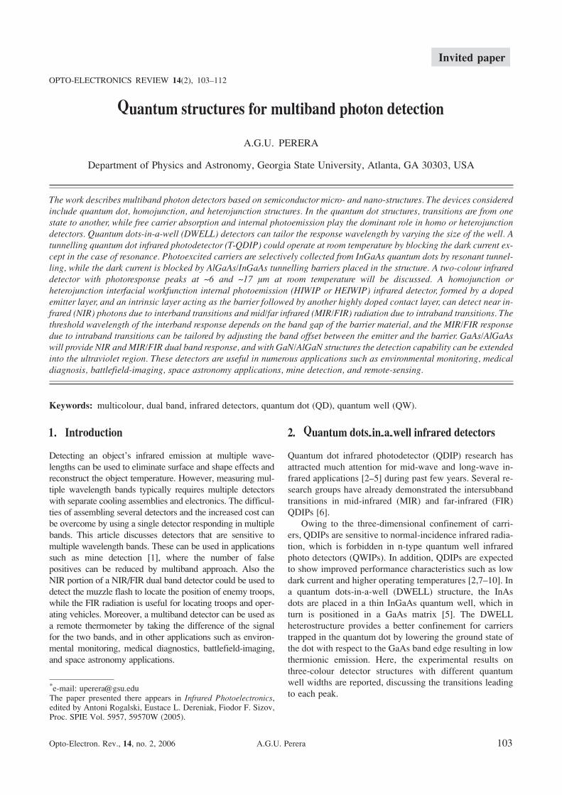
The variation of the dark current density of samples
1299, 1373, and 1388 with bias voltage at 77 K is shown in
Fig. 4. The symmetry observed for 1388 compared with
other two samples is due to the symmetry of the structure.
In 1388, the dots are placed symmetrically in the well. That
is the two well layers have the same thickness. But for
1373, and 1299, the thicknesses of the two InGaAs well
layers are different, making an asymmetric structure.
Among all these detectors, 1388 showed the lowest dark
current, and hence the highest detectivity of ~7.9×10¹⁰
Jones at 4.6 K under –2.2 V bias and 3.2×10¹⁰ Jones at 80
Opto-Electron. Rev., 14, no. 2, 2006 A.G.U. Perera 105
Invited paper
Fig. 2. The first two peaks of the three detectors at 4.6 K under –1.4
V and –0.5 V bias. The band diagram showing the transitions
leading to each peak is given in the inset and the transition states for
1388 are the same as 1373. Arrows indicate the peak positions and
× sign implies that the curve has been multiplied by the number
indicated.
Fig. 3. The FIR response of 1388 at different bias values (negative indicates that the top contact is negative). The band diagram represents
the transition leading to the response. The inset shows the responsivity at high temperature (72 K and 79 K) (a). The variation of the peak
responsivity of 1388 detector with applied bias and the corresponding transition between the states in the dot with bias (b).
K under –1.4 V bias was reported at 23.3 µm wavelength.
All but the FIR peak of 1373 were observed up to 80 K
while the FIR peak of 1373 could be obtained up to 60 K.
A GaAs/AlGaAs QWIP broadband detector, sensitive in
10–16 µm spectral range with a detectivity of ~1010 at 55
K, has been reported by Bandara et al. [15] The improve-
ment in the operating temperature of FIR response of
DWELL detectors (up to 80 K), compared with a typical
FIR QWIP [16] operating at ~10–20 K, proves the benefit
of the quasi-zero dimensional confinement.
According to the experimental results [12], the FIR peak
stays almost at the same position (~23.3 µm) for sample,
1299 and 1388. Changing the width of the quantum well
does not affect states in the quantum dot and this confirms
that the FIR peak is due to transitions between dot states.
Due to the fact that the dot size of 1373 has been increased
causing the energy difference between dot states to decrease,
the FIR peak of 1373 has shifted to ~25.5 µm. The three
peaks of DWELL detectors are expected to respond differ-
ently to polarized radiation. Hence, the energy states, and the
transitions leading to each peak of DWELL detectors can be
further explained by polarization measurements.
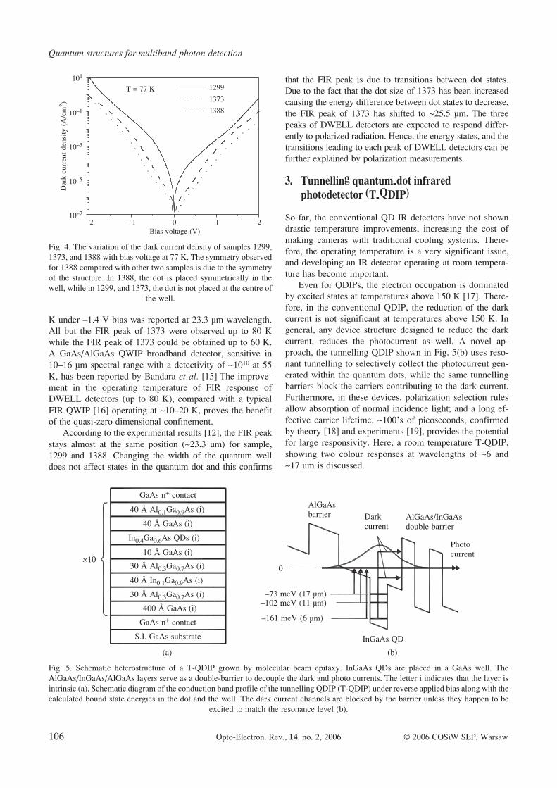
3. Tunnelling quantum-dot infraredphotodetector (T-QDIP)
So far, the conventional QD IR detectors have not shown
drastic temperature improvements, increasing the cost of
making cameras with traditional cooling systems. There-
fore, the operating temperature is a very significant issue,
and developing an IR detector operating at room tempera-
ture has become important.
Even for QDIPs, the electron occupation is dominated
by excited states at temperatures above 150 K [17]. There-
fore, in the conventional QDIP, the reduction of the dark
current is not significant at temperatures above 150 K. In
general, any device structure designed to reduce the dark
current, reduces the photocurrent as well. A novel ap-
proach, the tunnelling QDIP shown in Fig. 5(b) uses reso-
nant tunnelling to selectively collect the photocurrent gen-
erated within the quantum dots, while the same tunnelling
barriers block the carriers contributing to the dark current.
Furthermore, in these devices, polarization selection rules
allow absorption of normal incidence light; and a long ef-
fective carrier lifetime, ~100’s of picoseconds, confirmed
by theory [18] and experiments [19], provides the potential
for large responsivity. Here, a room temperature T-QDIP,
showing two colour responses at wavelengths of ~6 and
~17 µm is discussed.
Quantum structures for multiband photon detection
106 Opto-Electron. Rev., 14, no. 2, 2006 © 2006 COSiW SEP, Warsaw
Fig. 4. The variation of the dark current density of samples 1299,
1373, and 1388 with bias voltage at 77 K. The symmetry observed
for 1388 compared with other two samples is due to the symmetry
of the structure. In 1388, the dot is placed symmetrically in the
well, while in 1299, and 1373, the dot is not placed at the centre of
the well.
Fig. 5. Schematic heterostructure of a T-QDIP grown by molecular beam epitaxy. InGaAs QDs are placed in a GaAs well. The
AlGaAs/InGaAs/AlGaAs layers serve as a double-barrier to decouple the dark and photo currents. The letter i indicates that the layer is
intrinsic (a). Schematic diagram of the conduction band profile of the tunnelling QDIP (T-QDIP) under reverse applied bias along with the
calculated bound state energies in the dot and the well. The dark current channels are blocked by the barrier unless they happen to be
excited to match the resonance level (b).
3.1. Device structure
The T-QDIP structure, grown by molecular beam epitaxy,
is schematically shown in Fig. 5(a). The GaAs and AlGaAs
layers were grown at 610°C and the quantum dot layers
were grown at 500°C. Vertical circular mesa for top illumi-
nations were fabricated by standard photolithography, wet
chemical etching and contact metallization techniques. The
n-type top ring contact and the bottom contact were formed
by evaporated Ni/Ge/Au/Ti/Au with thickness of 50/325/
650/200/2000 �. The radius of the optically active area
varies from 100–300 µm. Devices for testing are mounted
on to chip carriers with silver epoxy and gold wire contacts
were made from the device to the chip carrier leads.
Figure 5(b) shows the band diagram under an applied
reverse bias. The double-barrier resonant tunnelling hetero-
structure serves to decouple the dark- and photocurrents. A
single Al0.1Ga0.9As barrier has been introduced on the other
side of the dot to create a quantum well, in which well-
defined quasi-bound final states are available for photo-ex-
cited electrons. The structure is designed so that these
states resonate with the tunnelling states in the In0.1Ga0.9As/
Al0.3Ga0.7As double barrier system. For photoexcited carri-
ers with energy equal to the energy difference between QD
bound state and well final state, the tunnelling probability
is near unity as confirmed by calculations. The energy
states in the quantum dot, and the well were calculated by
an eight-band k× p model [20], and solving the one dimen-
sional Schrödinger equation including the presence of the
wetting layer, respectively.
3.2. Results and discussion
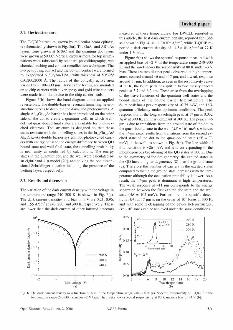
The variation of the dark current density with the voltage in
the temperature range 240–300 K, is shown in Fig. 6(a).
The dark current densities at a bias of 1 V are 0.21, 0.96,
and 1.55 A/cm2 at 240, 280, and 300 K, respectively. These
are lower than the dark current of other infrared detectors
measured at these temperatures. For DWELL reported in
this article, the best dark current density, reported for 1388
as shown in Fig. 4, is ~1.7×10⁴ A/cm2, while T-QDIP re-
ported a dark current density of ~4.3×10⁹ A/cm2 at 77 K
under 1-V bias.
Figure 6(b) shows the spectral response measured with
an applied bias of –2 V in the temperature range 240–300
K, and the inset shows the responsivity at 80 K under –3 V
bias. There are two distinct peaks observed at high temper-
ature, centred around ~6 and ~17 µm, and a weak response
around 11 µm. In addition, as seen in the responsivity curve
at 80 K, the 6-µm peak has split in to two closely spaced
peaks at 5.7 and 6.2 µm. These arise from the overlapping
of the wave functions of the quantum well states and the
bound states of the double barrier heterostructure. The
6-µm peak has a peak responsivity of ~0.75 A/W, and 16%
quantum efficiency under optimum conditions. The peak
responsivity of the long wavelength peak at 17 µm is 0.032
A/W at 300 K, and it is dominant at 300 K. The peak at ~6
µm is due to transitions from the ground state of the dot to
the quasi-bound state in the well (ÄE = 161 meV), whereas
the 17-µm peak results from transitions from the second ex-
cited state of the dot to the quasi-bound state (ÄE = 73
meV) in the well, as shown in Fig. 5(b). The line width of
this transition is ~26 meV, and it is corresponding to the
inhomogeneous broadening of the QD states at 300 K. Due
to the symmetry of the dot geometry, the excited states in
the QD have a higher degeneracy (8) than the ground state
(2). Therefore the number of carriers in the excited states
compared to that in the ground state increases with the tem-
perature although the occupation probability is lower. As a
result, the 17-µm peak is dominant at high temperatures.
The weak response at ~11 µm corresponds to the energy
separation between the first excited dot state and the well
state (ÄE = 102 meV). Furthermore, the specific detec-
tivity, D*, at 17 µm is on the order of 107 Jones at 300 K,
and with some re-designing of the device heterostructure,
D* ~109 Jones can be achieved under the same conditions.
Opto-Electron. Rev., 14, no. 2, 2006 A.G.U. Perera 107
Invited paper
Fig. 6. The dark current density as a function of bias in the temperature range 240–300 K (a). Spectral responsivity of T-QDIP in the
temperature range 240–300 K under –2 V bias. The inset shows spectral responsivity at 80 K under a bias of –3 V (b).

4. Interfacial workfunction detectors
A structure consisting of a top contact (p++ or n++) layer, an
emitter (p+ or n+) layer, an undoped barrier, and a bottom con-
tact layer (p++ or n++) can be either a homojunction or a
heterojunction interfacial workfunction internal photoemis-
sion (HIWIP or HEIWIP) detector based on the material in
the layers. HIWIPs have the same material in the emitters and
barriers, while HEIWIPs have different material in these lay-
ers. The detection mechanism involves free carrier absorption
in the emitter, followed by the internal photoemission of
photoexcited carriers across the junction barrier, and then the
collection of carriers by the applied electric field at the con-
tacts. The offset between the Fermi level in the emitter layer
and the valence band edge of the barrier layer gives the inter-
facial workfunction Ä. For HIWIPs, Ä arises due to the band
gap narrowing of a highly doped emitter layer [21], while for
HEIWIP, the band offset of different materials [22] also con-
tributes to Ä. The threshold wavelength ëc (in µm) is calcu-
lated by 1240/Ä, where Ä is in meV.
While recently reported dual band [1,23–25] and multi-
band [5,11,26,27] detectors can detect near-infrared (NIR),
mid-infrared (MIR), and far-infrared (FIR) radiation, the
HIWIP and HEIWIP detectors have the ability to detect a
much wider range of photons, even covering the UV and
FIR bands in a single structure. Both HIWIP and HEIWIP
detectors [21,22] were studied as FIR detectors. Here, the
focus will be on dual band detection. GaAs and Si based
HIWIP for NIR/FIR and GaN/AlGaN HEIWIP for UV/FIR
dual band detectors are presented in the next section.
4.1. Device structures
Figure 7(a) shows the schematic diagram of a HIWIP/
HEIWIP structure as processed. The emitter is doped,
while the barrier is undoped. Highly doped layers are used
for top and bottom contacts. The top contact and a part of
the emitter layer were etched out in order to allow front
side illuminations. The layer parameters (thickness and
doping level) of the sample were confirmed by secondary
ion mass spectrometry (SIMS). The mesas have different
sizes of optical windows and the spectral measurements
were carried out on a mesa showing the best dark current
characteristics. The GaAs HIWIP structure was grown by
metal organic chemical vapour deposition (MOCVD) tech-
nique at 610°C on a semi-insulating GaAs (100) substrate.
The Si HIWIP structure was grown on Si substrate, while
GaN HEIWIP structure was grown by MOCVD on sap-
phire substrate. The parameters corresponding to each layer
for all the structures are given in Table 1.
The band diagram of the HIWIP/HEWIP structures is
shown in Fig. 7(b). The photons (UV/NIR) with energy
above the band gap (Ä1) are absorbed in the barrier and
generate an electron-hole pair. The electron-hole pairs gen-
erated in the emitter would have to undergo internal photo-
emission before being collected. This process is the same
as for carriers generated by intraband transition in the emit-
ter. Due to this, they would have the same threshold as for
pairs generated in the barriers. Incident photons with en-
ergy below the band gap are absorbed in the emitter layer,
and photoexcited carriers (free carrier absorption) then un-
dergo internal photoemission across the barrier. The inter-
band threshold is determined by Ä1, while the interfacial
workfunction (Ä2) determines the FIR threshold. The
photoexcited carriers are finally swept out of the active re-
gion by the applied electric field and collected at the con-
tact. The detector was characterized by current-voltage
(IV) and spectral responsivity measurements from 4.6 K up
to the maximum possible temperature. The spectra were
obtained using a FTIR spectrometer with three beam split-
ters. The calibration of spectra was done by using a spec-
trum obtained with a Si composite bolometer with the same
combination of optical components. Since the detector re-
sponds in both bands under similar conditions, it is not tun-
able without exterior optical filtering.
Quantum structures for multiband photon detection
108 Opto-Electron. Rev., 14, no. 2, 2006 © 2006 COSiW SEP, Warsaw
Fig. 7. Schematic of a HIWIP/HEIWIP dual-band detector after processing. A window on the top of the device is made for front side
illumination (a). The band diagram of a p-type HIWIP/HEIWIP dual-band detector indicating both interband and intraband transitions
leading to UV/NIR and MIR/FIR responses, depending on the material (b).

4.2. NIR/FIR dual band detection
A GaAs based HIWIP structure with a p-doped emitter,
undoped barrier, and heavily doped top and bottom con-
tacts, with the parameters given in Table 1, was character-
ized. The NIR spectral response due to interband transi-
tions of carriers in the GaAs barrier layer is shown in Fig.
8(a). The solid line represents the experimental curve under
100 mV reverse (top contact is negative) bias, while the
dashed line represents the calculated curve based on a
model [28] in which the absorption coefficient for
interband transition was calculated using a permittivity
model [29]. With the band gap in GaAs being 1.51 eV, the
threshold wavelength observed at 0.82 µm confirms the
interband transition in GaAs. The oscillations seen in the
NIR region diminish with the applied electric field and the
temperature. As shown in the inset to Fig. 8(a), the small
peak at 0.819 µm (1.514 eV) is due to excitons [30] in
GaAs, and the amplitude increases with increasing bias.
The spectral responsivity curves due intraband mea-
sured from 4.6 to 20 K are shown in Fig. 8(b). The re-
sponse due to intraband transition is observed up to 70 µm
with a strong dependency on the temperature. Ä decreases
with the applied bias [21] giving rise to an increasing
threshold with bias. Ä of 18.4 meV corresponding to 67.5
µm threshold at 0.20 kV/cm field, and similarly, Ä of 16.5
meV giving 75 µm threshold at 0.50 kV/cm field have been
confirmed [31] based on both responsivity and Arrhenius
plots.
The oscillations in the MIR region observed are due to
Fabry-Perot interference arising from the 1 µm thick GaAs
barrier layer in the device structure. The sharp drop around
37 µm is due to the reststrahlen band of GaAs. The two
peaks at 57 and 63 µm are due to transitions of hydrogenic
impurity atoms in the barrier region from the impurity
ground state to the excited states [28]. These transitions
show a strong bias dependence due to the fact that the car-
riers excited to upper states must undergo tunnelling
through the barrier, formed by the Coulomb potential of the
acceptors, with the support of the external applied field.
An optimum responsivity of ~8 A/W and a detectivity
of ~6×10⁹ Jones were obtained at 0.8 µm for interband re-
sponse, while a responsivity of ~7 A/W and a detectivity of
~5×10⁹ Jones were reported at 57 µm, under 100-mV re-
verse bias at 20 K. The responsivity of the 63-µm and
57-µm peaks show a strong dependence with the tempera-
ture, and the 63-µm peak is dominant at higher tempera-
tures. This is caused presumably by the increased rate of
Opto-Electron. Rev., 14, no. 2, 2006 A.G.U. Perera 109
Invited paper
Table 1. The layer thickness (W), and the doping concentration (N) of the bottom contact (bc), barrier(b), emitter(e),
and top contact (tc), respectively, for three structures. The barriers of the Si HIWIP, and GaN/AlGaN HEIWIP
structures are undoped. The emitter of the GaN/AlGaN HEIWIP acts as the top contact.
Materialsystem
Structuretype
Wbc
(µm)Nbc
(1019cm–3)Wb
(µm)Nb
(1017cm–3)We
(nm)Ne
(1018cm–3)Wtc
(nm)Ntc
(1019cm–3)
GaAs HIWIP 1 2.0 1 1.8 200 15 120 5.3
Si HIWIP 1 1–1.5 1 – 200 2–3 100 1–1.5
GaN/AlGaN HEIWIP 0.7 0.5 0.6 – 200 5 – –
Fig. 8. The interband response fitted with a model for 100 mV reverse bias. The inset shows the bias dependence of the exciton peak at the
threshold end of the experimental response curve. The two curves for 10 and 20 mV reverse bias have been multiplied by 10 and 3 for
clarity (a). Interband and intraband responses at different temperatures at –50 mV bias. The left and right axes correspond to NIR and FIR,
responsivity, and a break on wavelength axis at 2 µm has been made in order to expand the view in both regions (b).

collecting carriers excited to the upper states from the im-
purity ground state at high temperature. If the rate of col-
lection of excited carriers by the external circuit is low, the
excited carriers either will relax back in to the ground state,
or occupy the excited states, resulting in a high population
density. At high temperature, the rate of collection of ex-
cited carriers over the barrier can be enhanced by the ther-
mal energy, leading to enhanced responsivity.
Similar to the GaAs HIWIP detector discussed, a Si
HIWIP detector having a highly p-doped Si bottom contact,
an undoped Si barrier, a p-doped Si emitter, and a highly
doped Si top contact has been tested. The layer parameters
are given in Table 1. As shown in Fig. 9, NIR threshold at
~1 µm corresponding to interband transitions in the Si bar-
rier, and FIR threshold at ~37.5 µm due to intraband transi-
tions in the p-doped emitter can be observed. Similar to the
GaAs HIWIP detector, the bias dependency of the sharp
peak at ~30 µm proves that the corresponding transition is
connected to the impurity states [28] in the structure. This
detector showed a response up to 30 K in both NIR and
FIR regions.
Liu et al. [24] reported a GaAs/AlGaAs QWIP visible/
MIR dual band detector based on interband and inter-
subband transitions in the structure. The well is n-doped,
and a large band gap top contact layer is used to open a
window for visible light. An MIR peak centred around 8.3
µm is obtained from the intersubband transitions between
the two confined states in the well. Visible photons in the
range 1.8–2.3 eV (0.7–0.55 µm) are absorbed in both well
and barrier layers. However, the photocurrent generated
from the transition from valence band of the well to the
first confined state in the well has a high probability to re-
combine before being collected. Hence, the major contribu-
tion for the visible response comes from the transitions to
the second confined state (close to the barrier) in the well.
Touse et al. [26] have demonstrated a multiple step quan-
tum well dual band detector responding in NIR and MIR
regions, based on similar detection mechanism. The step
quantum well is made of In0.1Ga0.9As/n-doped In0.3Ga0.7As
which in turn sandwiched in GaAs barriers. An MIR re-
sponse peak at 10.3 µm is obtained due to intersubband
transitions in the quantum well. An interband response is
observed in the wavelength range 0.82–0.95 µm due to
transitions from the valence band of the In0.3Ga0.7As well
to the second confined state in the conduction band of the
well. The photons with energy above the band gap of GaAs
(0.82 µm) is absorbed in the GaAs barrier layer, and this
determines the lower wavelength limit of the interband re-
sponse.
4.3. UV/IR HEIWIP dual band detector
A modification of the HIWIP structure with GaN/AlGaN, a
solar blind UV/IR dual band structure is also feasible. UV
detectors are used in numerous areas such as military, biol-
ogy, and environmental research. The structure considered
is grown on sapphire substrate, and n-doped GaN and
undoped AlGaN are used for the emitter and the barrier, re-
spectively. A doped GaN layer is used as the bottom con-
tact, while the emitter itself acts as the top contact. The
layer parameters are given in Table 1. A GaN/AlGaN UV
detector can detect UV radiation by interband absorption in
the AlGaN barrier layer. UV detectors have already been
demonstrated by several groups [32–34] using GaN/AlGaN
system. Intraband transitions giving rise to IR absorption in
GaN/AlGaN is similar to that in GaAs/AlGaAs HEIWIP
detectors [35]. Preliminary measurements in both UV and
IR regions, as shown in Fig. 10, show better performance
in both regions. The interband response leading to UV de-
tection can be obtained at room temperature. The
UV-threshold observed is 360 nm, and it is in good agree-
ment with the band gap of AlGaN. The intraband threshold
is observed at ~400 µm at 5.3 K, and this promotes the de-
velopment of terahertz GaN detectors. Due to strong TO
phonon-photon interaction and phonon absorption, a deep
valley at ~18 µm in the responsivity curve of a GaN/AlGaN
detector (~37 µm for GaAs/AlGaAs) is observed. Further-
more, expected results are in good agreement with the theo-
retical model in both UV and IR bands, and the inset to Fig.
10(b) shows the MIR response fitted with the theoretical
model. The IR response with 14 µm threshold can be ob-
tained up to 80 K. Compared to the GaAs/AlGaAs system,
GaN/AlGaN has advantages in controlling the Al fraction
over a wide range, and the broad continuous spectral re-
sponse range.
This approach could be used to develop dualband detec-
tors tailored to specific applications. By adjusting the mate-
rial in the layers, the thresholds for the interband and
intraband responses can be tailored separately. For exam-
Quantum structures for multiband photon detection
110 Opto-Electron. Rev., 14, no. 2, 2006 © 2006 COSiW SEP, Warsaw
Fig. 9. The interband response of Si HIWIP dual band detector at
4.6 K under 1-V reverse bias, and intraband response under 1, and 2
V reverse bias at 4.6 K. NIR-threshold observed at ~1 ìm is
corresponding to the band gap of intrinsic Si. The FIR threshold is
observed at ~37.5 ìm. The response in both bands can be obtained
up to 30 K. The left and right axes correspond to NIR and FIR,
respectively, and a break on wavelength axis at 1.1 ìm has been
made in order to expand the view in both regions.

ple, in an AlGaN based detector, if the Al fraction is varied
in both the emitter and barrier by the same amount, the
intraband threshold will not be changed while the interband
threshold will change. Alternatively varying only the emit-
ter Al fraction, the intraband threshold could be varied
without changing the interband threshold. Moreover, the
resonant cavity effects can be used to tailor the IR response
peak to the desired wavelength. By adjusting the materials
it should be possible to tune the interband threshold from
the UV to NIR and the intraband threshold from the MIR to
the FIR. That is, the reported dual band approach with
HIWIP/HEIWIP detectors can be tested with any material
such as InN, InGaN, GaN, AlGaN, and AlN. InN could
give an interband response in NIR, while InGaN could re-
spond in NIR-Visible region. A UV interband response
could be expected from an AlN based detector. Also, as the
response for the two processes originates at different loca-
tions, it may be possible to design a device that is capable
of separately measuring both components simultaneously.
Ä determines the IR threshold, and lowering the Ä will in-
crease the dark current, resulting in a lowering of the oper-
ating temperature of the detector. In another word, any
HIWIP/HEIWIP design focused on increased threshold
will reduce the operating temperature. One of the possibili-
ties to increase the operating temperature is to use the reso-
nance tunnelling approach, in which the photocurrent is se-
lectively collected by incorporating tunnelling barriers in to
the structure. Furthermore, different design possibilities to
increase the performance of the detector will be studied.
5. Conclusions
In summary, multiband photon detection covering MIR/
FIR, NIR/MIR/FIR, UV/MIR, and UV/FIR has been dis-
cussed. Based on the results, the transitions leading to each
peak of DWELL detectors are explained. Room tempera-
ture operation of T-QDIP is made possible by incorporat-
ing tunnelling barriers. HIWIP/HEIWIP detectors can de-
tect NIR or UV, and MIR/FIR radiation, due to interband
and intraband transitions within the structure. By adjusting
the material, the threshold of the interband and intraband
responses can be tailored. Based on theoretical models and
experimental data, the transition leading to each bands are
explained. High performances of the detectors demonstrate
the potential applications where the detection in multi-
bands is important.
Acknowledgements
This work is supported in part by the NSF under grant No.
ECS-0553051. The author would like to acknowledge Dr
H.C. Liu at NRC Canada for his support throughout our IR
detector development. The author also acknowledges Profs.
P. Bhattacharya, S. Krishna, V.I. Gavrilenko, B.N.
Zvonkov, N. Dietz, I.T. Ferguson, V. Apalkov, and Drs
S.G. Matsik, D.G. Esaev, and Z.G. Hu, Mr M.B.M. Rinzan,
G. Ariyawansa, and M. Alevil.
References
1. A. Goldberg, P.N. Uppal, and M. Winn, “Detection of bur-
ied land mines using a dual-band LWIR/LWIR QWIP focal
plane array”, Infrared Phys. & Technol. 44, 427 (2003).
2. B. Kochman, A.D. Stiff-Roberts, S. Chakrabarti, J.D. Phil-
lips, S. Krishna, J. Singh, and P. Bhattacharya, “Absorption,
carrier lifetime, and gain in InAs-GaAs quantum-dot infra-
red photodetectors”, IEEE. J. Quant. Electron. 39, 459
(2003).
3. H.C. Liu, M. Gao, J. McCaffrey, Z.R. Wasilewski, and S.
Fafard, “Quantum dot infrared photodetectors”, Appl. Phys.
Lett. 78, 79 (2001).
4. L. Jiang, S.S. Li, N.T. Yeh, J.I. Chyi, C.E. Ross, and K.S.
Jones, “In0.6Ga0.4As/GaAs quantum-dot infrared photode-
Opto-Electron. Rev., 14, no. 2, 2006 A.G.U. Perera 111
Invited paper
Fig. 10. UV response of GaN/AlGaN HEIWIP dual band detector, arising due to interband transitions in AlGaN barrier layer at 300 K. A
UV-threshold, observed at 360 nm under 0.1 V reverse bias at 300 K, is corresponding to the band gap of AlxGa1–xN with x = 0.026 (a). IR
response with an FIR threshold of ~400 µm at 5.3 K under –0.5 V bias. The inset shows the MIR response fitted with the theoretical model (b).

tector with operating temperature up to 260 K”, Appl. Phys.
Lett. 82, 1986–1988 (2003).
5. A. Raghavan, P. Rotella, A. Stintz, B. Fuchs, S. Krishna, C.
Morath, D.A. Cardimona, and S.W. Kennerly, “High-res-
ponsivity, normal-incidence long-wave infrared (lp ~7.2 µm)
InAs/In0.15Ga0.85As dots-in-a-well detector”, Appl. Phys.
Lett. 81, 1369 (2002).
6. B. Aslan, H.C. Liu, M. Korkusinski, S.J. Cheng, and P.
Hawrylak, “Response spectra from mid- to far-infrared, polar-
ization behaviors, and effects of electron numbers in quan-
tum-dot photodetectors”, Appl. Phys. Lett. 82, 639 (2003).
7. Z. Ye and J.C. Campbell, “InAs quantum dot infrared
photodetectors with In0.15Ga0.85As strain-relief cap layers”,
J. Appl. Phys. 92, 7462–7468 (2002).
8. J. Phillips, K. Kamath, and P. Bhattacharya, “Far-infrared
photoconductivity in self-organized InAs quantum dots”,
Appl. Phys. Lett. 72, 2020 (1998).
9. S. Maimon, E. Finkman, and G. Bahir, “Intersublevel tran-
sitions in InAs/GaAs quantum dots infrared photodetec-
tors”, Appl. Phys. Lett. 73, 2003 (1998).
10. D. Pan, E. Towe, and S. Kennerly, “Normal-incidence
intersubband (In,Ga)As/GaAs quantum dot infrared photo-
detectors”, Appl. Phys. Lett. 73, 1937 (1998).
11. S. Krishna, S. Raghavan, G. von Winckel, A. Stintz, G.
Ariyawansa, S.G. Matsik, and A.G.U. Perera, “Three-colour
(lp1 ~3.8 µm, lp2 ~8.5 µm, and lp3 ~23.2 µm) InAs/InGaAs
quantum-dots-in-a-well detector”, Appl. Phys. Lett. 83,
2745–2747 (2003).
12. G. Ariyawansa, A.G.U. Perera, G.S. Raghavan, G. von
Winckel, A. Stintz, and S. Krishna, “Effect of well width on
three colour quantum dots-in-a-well infrared detectors”,
IEEE Photon. Technol. Lett. 17, 1064 (2005).
13. B.F. Levine, “Quantum-well infrared photodetectors”, J.
Appl. Phys., 74, R1–R81 (1993).
14. A. Amtout, S. Raghavan, P. Rotella, G. v. Winckel, A.
Stintz, and S. Krishna, “Theoretical modeling and experi-
mental characterization of InAs/InGaAs quantum dots in a
well detector”, J. Appl. Phys. 96, 3782–3786 (2004).
15. S.V. Bandara, S.D. Gunapala, J.K. Liu, E.M. Luong, J.M.
Mumolo, W. Hong, D.K. Sengupta, and M.J. McKelvey,
“10–16 µm broad band quantum well infrared photode-
tector”, Appl. Phys. Lett. 72, 2427 (1998).
16. A.G.U. Perera, W.Z. Shen, S.G. Matsik, H.C. Liu, M. Bu-
chanan, and W.J. Schaff, “GaAs/AlGaAs quantum well
photodetectors with a cutoff wavelength at 28 µm”, Appl.
Phys. Lett. 72, 1596–1598 (1998).
17. P. Bhattacharya, X.H. Su, S. Chakrabarti, G. Ariyawansa,
and A.G.U. Perera, “Characteristics of a tunnelling quantum
dot infrared photodetector operating at room temperature”,
Appl. Phys. Lett. 86, 191106 (2005).
18. J. Urayama, T.B. Norris, J. Singh, and P. Bhattacharya,
“Observation of phonon bottleneck in quantum dot elec-
tronic relaxation”, Phys. Rev. Lett. 86, 4930 (2001).
19. E. Kim, A. Madhukar, Z. Ye, and J.C. Campbell, “High
detectivity InAs quantum dot infrared photodetectors”,
Appl. Phys. Lett. 84, 3277 (2004).
20. H. Jiang and J. Singh, “Strain distribution and electronic
spectra of InAs/GaAs self-assembled dots: An eight-band
study”, Phys. Rev. B56, 4696–4701 (1997).
21. W.Z. Shen, A.G.U. Perera, H.C. Liu, M. Buchanan, and
W.J. Schaff, “Bias effects in high performance GaAs homo-
junction far-infrared detectors”, Appl. Phys. Lett. 71,
2677–2679 (1997).
22. D.G. Esaev, M.B.M. Rinzan, S.G. Matsik, and A.G.U.
Perera, “Design and optimization of GaAs/AlGaAs hetero-
junction infrared detectors”, J. Appl. Phys. 96, 4588–4597
(2004).
23. H.C. Liu, P.H. Wilson, M. Lamm, A.G. Steele, Z.R.
Wasilewski, J. Li, M. Buchanan, and J.G. Simmonsa, “Low
dark current dual band infrared photodetector using thin
AlAs barriers and G-X mixed intersubband transition in
GaAs quantum wells”, Appl. Phys. Lett. 64, 475 (1994).
24. H.C. Liu, C.Y. Song, A. Shen, M. Gao, Z.R. Wasilewski,
and M. Buchanan, “GaAs/AlGaAs quantum-well photode-
tector for visible and middle infrared dual-band detection”,
Appl. Phys. Lett. 77, 2437 (2000).
25. M.P. Touse, G. Karunasiri, K.R. Lantz, H. Li, and T. Mei,
“Near- and mid-infrared detection using GaAs/InxGa1xAs/
InyGa1yAs multiple step quantum wells”, Appl. Phys. Lett.
86, 093501-1 (2005).
26. K.K. Choi, B.F. Levine, C.G. Bethea, J. Walker, and R.J.
Malik, “Infrared photoelectron tunnelling spectroscopy of
strongly coupled quantum wells”, Phys. Rev. B39, 8029
(1989).
27. S. Chakrabarti, X.H. Su, P. Bhattacharya, G. Ariyawansa,
and A.G.U. Perera, “Characteristics of a multicolour
InGaAs–GaAs quantum-dot infrared photodetector”, IEEE
Photon. Technol. Lett. 17, 178–180 (2005).
28. D.G. Esaev, M.B.M. Rinzan, S.G. Matsik, A.G.U. Perera,
H.C. Liu, B.N. Zvonkov, V.I. Gavrilenko, and A.A.
Belyanin, “High performance single emitter homojunction
interfacial work function far infrared detectors”, J. Appl.
Phys. 95, 512–519 (2004).
29. S. Adachi, “Refractive indices of III–V compounds: Key
properties of InGaAsP relevant to device design”, J. Appl.
Phys. 53, 5863 (1982).
30. M.D. Sturge, “Optical absorption of gallium arsenide be-
tween 0.6 and 2.75 eV”, Phys. Rev. 127, 768 (1962).
31. G. Ariyawansa, M.B.M. Rinzan, D.G. Esaev, S.G. Matsik,
G. Hastings, A.G.U. Perera, H.C. Liu, B.N. Zvonkov, and
V.I. Gavrilenko, “Near- and far-infrared p-GaAs dual-band
detector”, Appl. Phys. Lett. 86, 143510–143513 (2005).
32. F. Binet, J.Y. Duboz, E. Rosencher, F. Scholz, and V.
Harle, “Mechanisms of recombination in GaN photode-
tectors”, Appl. Phys. Lett. 69, 1202 (1996).
33. S.K. Zhang, W.B. Wang, I. Shtau, F. Yun, L. He, H.
Morkoc, X. Zhou, M. Tamargo, R.R. Alfano, “Backillumi-
nated GaN/AlGaN heterojunction ultraviolet photodetector
with high internal gain”, Appl. Phys. Lett. 81, 4862 (2002).
34. E. Monroy, F. Omnes, and F. Calle, “Wide-bandgap semi-
conductor ultraviolet photodetectors”, Semicond. Sci.
Technol. 18, R33–R51 (2003).
35. S.G. Matsik, M.B.M. Rinzan, D.G. Esaev, A.G.U. Perera,
H.C. Liu, and M. Buchanan, “20 µm cutoff heterojunction
interfacial work function internal photoemission detectors”,
Appl. Phys. Lett. 84, 3435–3437 (2004).
Quantum structures for multiband photon detection
112 Opto-Electron. Rev., 14, no. 2, 2006 © 2006 COSiW SEP, Warsaw