Quantum dot SOA/silicon external cavity multi- wavelength...
6
Quantum dot SOA/silicon external cavity multi- wavelength laser Yi Zhang, 1,2,4 Shuyu Yang, 1,2,4,* Xiaoliang Zhu, 3 Qi Li, 3 Hang Guan, 3 Peter Magill, 2 Keren Bergman, 3 Thomas Baehr-Jones, 2 and Michael Hochberg 2 1 Department of Electrical and Computer Engineering, University of Delaware, Newark, DE, 19716 USA 2 Coriant Advanced Technology Group, New York, NY, 10011 USA 3 Department of Electrical Engineering, Columbia University, New York, NY 10027 USA 4 contributed equally * [email protected] Abstract: We report a hybrid integrated external cavity, multi-wavelength laser for high-capacity data transmission operating near 1310 nm. This is the first demonstration of a single cavity multi-wavelength laser in silicon to our knowledge. The device consists of a quantum dot reflective semiconductor optical amplifier and a silicon-on-insulator chip with a Sagnac loop mirror and microring wavelength filter. We show four major lasing peaks from a single cavity with less than 3 dB power non-uniformity and demonstrate error-free 4 × 10 Gb/s data transmission. ©2015 Optical Society of America OCIS codes: (140.5960) Semiconductor lasers; (250.5300) Photonic integrated circuits; (130.0250) Optoelectronics. References and links 1. Cisco visual networking index (ciscovni.com). 2. R. Soref, “The past, present, and future of silicon photonics,” IEEE J. Sel. Top. Quantum Electron. 12(6), 1678– 1687 (2006). 3. G. T. Reed, G. Mashanovich, F. Y. Gardes, and D. J. Thomson, “Silicon optical modulators,” Nat. Photonics 4(8), 518–526 (2010). 4. J. Michel, J. F. Liu, and L. C. Kimerling, “High-performance Ge-on-Si photodetectors,” Nat. Photonics 4(8), 527–534 (2010). 5. M. Hochberg, N. Harris, R. Ding, Y. Zhang, A. Novack, Z. Xuan, and T. Baehr-Jones, “Silicon photonics: the next fabless semiconductor industry,” IEEE Solid State Circuits Mag. 5(1), 48–58 (2013). 6. B. Analui, D. Guckenberger, D. Kucharski, and A. Narasimha, “A fully integrated 20-Gb/s optoelectronic transceiver implemented in a standard 0.13-μm CMOS SOI technology,” IEEE J. Solid-State Circuits 41(12), 2945–2955 (2006). 7. B. G. Lee, A. V. Rylyakov, W. M. J. Green, S. Assefa, C. W. Baks, R. Rimolo-Donadio, D. M. Kuchta, M. H. Khater, T. Barwicz, C. Reinholm, E. Kiewra, S. M. Shank, C. L. Schow, and Y. A. Vlasov, “Monolithic silicon integration of scaled photonic switch fabrics, CMOS logic, and device driver circuits,” J. Lightwave Technol. 32(4), 743–751 (2014). 8. C. R. Doerr, L. Chen, D. Vermeulen, T. Nielsen, S. Azemati, S. Stulz, G. McBrien, X.-M. Xu, B. Mikkelsen, M. Givehchi, C. Rasmussen, and S. Y. Park, “Single-chip silicon photonics 100-Gb/s coherent transceiver,” in Optical Fiber Communication Conference, paper Th5C.1 (2014). 9. Q. Xu, B. Schmidt, S. Pradhan, and M. Lipson, “Micrometre-scale silicon electro-optic modulator,” Nature 435(7040), 325–327 (2005). 10. G. Li, A. V. Krishnamoorthy, I. Shubin, J. Yao, Y. Luo, H. Thacker, X. Zheng, K. Raj, and J. E. Cunningham, “Ring resonator modulators in silicon for interchip photonic links,” IEEE J. Sel. Top. Quantum Electron. 19(6), 3401819 (2013). 11. P. Dong, W. Qian, H. Liang, R. Shafiiha, D. Feng, G. Li, J. E. Cunningham, A. V. Krishnamoorthy, and M. Asghari, “Thermally tunable silicon racetrack resonators with ultralow tuning power,” Opt. Express 18(19), 20298–20304 (2010). 12. S.-H. Jeong, D. Shimura, T. Simoyama, M. Seki, N. Yokoyama, M. Ohtsuka, K. Koshino, T. Horikawa, Y. Tanaka, and K. Morito, “Low-loss, flat-topped and spectrally uniform silicon-nanowire-based 5th-order CROW fabricated by ArF-immersion lithography process on a 300-mm SOI wafer,” Opt. Express 21(25), 30163–30174 (2013). 13. K. Padmaraju, J. Chan, L. Chen, M. Lipson, and K. Bergman, “Thermal stabilization of a microring modulator using feedback control,” Opt. Express 20(27), 27999–28008 (2012). 14. L. Vivien, A. Polzer, D. Marris-Morini, J. Osmond, J. M. Hartmann, P. Crozat, E. Cassan, C. Kopp, H. Zimmermann, and J. M. Fédéli, “Zero-bias 40Gbit/s germanium waveguide photodetector on silicon,” Opt. Express 20(2), 1096–1101 (2012). #228970 - $15.00 USD Received 8 Dec 2014; revised 4 Feb 2015; accepted 5 Feb 2015; published 13 Feb 2015 © 2015 OSA 23 Feb 2015 | Vol. 23, No. 4 | DOI:10.1364/OE.23.004666 | OPTICS EXPRESS 4666
Transcript of Quantum dot SOA/silicon external cavity multi- wavelength...

Quantum dot SOA/silicon external cavity multi-wavelength laser
Yi Zhang,1,2,4 Shuyu Yang,1,2,4,* Xiaoliang Zhu,3 Qi Li,3 Hang Guan,3 Peter Magill,2 Keren Bergman,3 Thomas Baehr-Jones,2 and Michael Hochberg2
1Department of Electrical and Computer Engineering, University of Delaware, Newark, DE, 19716 USA 2Coriant Advanced Technology Group, New York, NY, 10011 USA
3Department of Electrical Engineering, Columbia University, New York, NY 10027 USA 4contributed equally
Abstract: We report a hybrid integrated external cavity, multi-wavelength laser for high-capacity data transmission operating near 1310 nm. This is the first demonstration of a single cavity multi-wavelength laser in silicon to our knowledge. The device consists of a quantum dot reflective semiconductor optical amplifier and a silicon-on-insulator chip with a Sagnac loop mirror and microring wavelength filter. We show four major lasing peaks from a single cavity with less than 3 dB power non-uniformity and demonstrate error-free 4 × 10 Gb/s data transmission.
©2015 Optical Society of America
OCIS codes: (140.5960) Semiconductor lasers; (250.5300) Photonic integrated circuits; (130.0250) Optoelectronics.
References and links
1. Cisco visual networking index (ciscovni.com). 2. R. Soref, “The past, present, and future of silicon photonics,” IEEE J. Sel. Top. Quantum Electron. 12(6), 1678–
1687 (2006). 3. G. T. Reed, G. Mashanovich, F. Y. Gardes, and D. J. Thomson, “Silicon optical modulators,” Nat. Photonics
4(8), 518–526 (2010). 4. J. Michel, J. F. Liu, and L. C. Kimerling, “High-performance Ge-on-Si photodetectors,” Nat. Photonics 4(8),
527–534 (2010). 5. M. Hochberg, N. Harris, R. Ding, Y. Zhang, A. Novack, Z. Xuan, and T. Baehr-Jones, “Silicon photonics: the
next fabless semiconductor industry,” IEEE Solid State Circuits Mag. 5(1), 48–58 (2013). 6. B. Analui, D. Guckenberger, D. Kucharski, and A. Narasimha, “A fully integrated 20-Gb/s optoelectronic
transceiver implemented in a standard 0.13-µm CMOS SOI technology,” IEEE J. Solid-State Circuits 41(12), 2945–2955 (2006).
7. B. G. Lee, A. V. Rylyakov, W. M. J. Green, S. Assefa, C. W. Baks, R. Rimolo-Donadio, D. M. Kuchta, M. H. Khater, T. Barwicz, C. Reinholm, E. Kiewra, S. M. Shank, C. L. Schow, and Y. A. Vlasov, “Monolithic silicon integration of scaled photonic switch fabrics, CMOS logic, and device driver circuits,” J. Lightwave Technol. 32(4), 743–751 (2014).
8. C. R. Doerr, L. Chen, D. Vermeulen, T. Nielsen, S. Azemati, S. Stulz, G. McBrien, X.-M. Xu, B. Mikkelsen, M. Givehchi, C. Rasmussen, and S. Y. Park, “Single-chip silicon photonics 100-Gb/s coherent transceiver,” in Optical Fiber Communication Conference, paper Th5C.1 (2014).
9. Q. Xu, B. Schmidt, S. Pradhan, and M. Lipson, “Micrometre-scale silicon electro-optic modulator,” Nature 435(7040), 325–327 (2005).
10. G. Li, A. V. Krishnamoorthy, I. Shubin, J. Yao, Y. Luo, H. Thacker, X. Zheng, K. Raj, and J. E. Cunningham, “Ring resonator modulators in silicon for interchip photonic links,” IEEE J. Sel. Top. Quantum Electron. 19(6), 3401819 (2013).
11. P. Dong, W. Qian, H. Liang, R. Shafiiha, D. Feng, G. Li, J. E. Cunningham, A. V. Krishnamoorthy, and M. Asghari, “Thermally tunable silicon racetrack resonators with ultralow tuning power,” Opt. Express 18(19), 20298–20304 (2010).
12. S.-H. Jeong, D. Shimura, T. Simoyama, M. Seki, N. Yokoyama, M. Ohtsuka, K. Koshino, T. Horikawa, Y. Tanaka, and K. Morito, “Low-loss, flat-topped and spectrally uniform silicon-nanowire-based 5th-order CROW fabricated by ArF-immersion lithography process on a 300-mm SOI wafer,” Opt. Express 21(25), 30163–30174 (2013).
13. K. Padmaraju, J. Chan, L. Chen, M. Lipson, and K. Bergman, “Thermal stabilization of a microring modulator using feedback control,” Opt. Express 20(27), 27999–28008 (2012).
14. L. Vivien, A. Polzer, D. Marris-Morini, J. Osmond, J. M. Hartmann, P. Crozat, E. Cassan, C. Kopp, H. Zimmermann, and J. M. Fédéli, “Zero-bias 40Gbit/s germanium waveguide photodetector on silicon,” Opt. Express 20(2), 1096–1101 (2012).
#228970 - $15.00 USD Received 8 Dec 2014; revised 4 Feb 2015; accepted 5 Feb 2015; published 13 Feb 2015 © 2015 OSA 23 Feb 2015 | Vol. 23, No. 4 | DOI:10.1364/OE.23.004666 | OPTICS EXPRESS 4666

15. Y. Zhang, S. Yang, Y. Yang, M. Gould, N. Ophir, A. E.-J. Lim, G.-Q. Lo, P. Magill, K. Bergman, T. Baehr-Jones, and M. Hochberg, “A high-responsivity photodetector absent metal-germanium direct contact,” Opt. Express 22(9), 11367–11375 (2014).
16. G. Kurczveil, M. J. R. Heck, J. D. Peters, J. M. Garcia, D. Spencer, and J. E. Bowers, “An integrated hybrid silicon multiwavelength AWG laser,” IEEE J. Sel. Top. Quantum Electron. 17(6), 1521–1527 (2011).
17. S. Keyvaninia, S. Verstuyft, S. Pathak, F. Lelarge, G.-H. Duan, D. Bordel, J.-M. Fedeli, T. De Vries, B. Smalbrugge, E. J. Geluk, J. Bolk, M. Smit, G. Roelkens, and D. Van Thourhout, “III-V-on-silicon multi-frequency lasers,” Opt. Express 21(11), 13675–13683 (2013).
18. V. Ataie, E. Temprana, L. Liu, Y. Myslivets, P. Kuo, Ni. Alic, and S. Radic, “Flex-grid compatible ultra wide frequency comb source for 31.8 Tb/s coherent transmission of 1520 UDWDM channels,” in Optical Fiber Communication Conference, paper Th5B (2014).
19. P. Del’Haye, A. Schliesser, O. Arcizet, T. Wilken, R. Holzwarth, and T. J. Kippenberg, “Optical frequency comb generation from a monolithic microresonator,” Nature 450(7173), 1214–1217 (2007).
20. M. A. Foster, J. S. Levy, O. Kuzucu, K. Saha, M. Lipson, and A. L. Gaeta, “Silicon-based monolithic optical frequency comb source,” Opt. Express 19(15), 14233–14239 (2011).
21. C. H. Henry, P. S. Henry, and M. E. Lax, “Partition fluctuations in nearly single-longitudinal-mode lasers,” J. Lightwave Technol. 2(3), 209–216 (1984).
22. Y. Okano, K. Nakagawa, and T. Ito, “Laser mode partition noise evaluation for optical fiber transmission,” IEEE Trans. Commun. 28(2), 238–243 (1980).
23. A. Kovsh, I. Krestnikov, D. Livshits, S. Mikhrin, J. Weimert, and A. Zhukov, “Quantum dot laser with 75 nm broad spectrum of emission,” Opt. Lett. 32(7), 793–795 (2007).
24. A. Gubenko, I. Krestnikov, D. Livshtis, S. Mikhrin, A. Kovsh, L. West, C. Bornholdt, N. Grote, and A. Zhukov, “Error-free 10 Gbit/s transmission using individual Fabry-Perot modes of low-noise quantum-dot laser,” Electron. Lett. 43(25), 1430–1431 (2007).
25. A. Capua, L. Rozenfeld, V. Mikhelashvili, G. Eisenstein, M. Kuntz, M. Laemmlin, and D. Bimberg, “Direct correlation between a highly damped modulation response and ultra low relative intensity noise in an InAs/GaAs quantum dot laser,” Opt. Express 15(9), 5388–5393 (2007).
26. http://www.innolume.com/products/Gain-chips.htm. 27. Y. Zhang, S. Yang, H. Guan, A. E.-J. Lim, G.-Q. Lo, P. Magill, T. Baehr-Jones, and M. Hochberg, “Sagnac loop
mirror and micro-ring based laser cavity for silicon-on-insulator,” Opt. Express 22(15), 17872–17879 (2014). 28. H. Debregeas, C. Ferrari, M. A. Cappuzzo, F. Klemens, R. Keller, F. Pardo, C. Bolle, C. Xie, and M. P.
Earnshaw, “2kHz linewidth C-band tunable laser by hybrid integration of reflective SOA and SiO2 PLC external cavity,” in IEEE International Semiconductor Conference, 50–51 (2014).
29. Y. Zhang, S. Yang, A. E.-J. Lim, G.-Q. Lo, C. Galland, T. Baehr-Jones, and M. Hochberg, “A compact and low loss Y-junction for submicron silicon waveguide,” Opt. Express 21(1), 1310–1316 (2013).
1. Introduction
The growth of Internet traffic due to the ever-increasing popularity of mobile devices, high-definition video, big data, and cloud computing [1] demands high-speed, low-cost and low power consumption communication technology. Silicon photonics is a promising platform for addressing such needs because it enables compact device footprints using a platform compatible with the manufacturing facilities used for complementary metal-oxide-semiconductor (CMOS) electronics. The last decade witnessed substantial progress in research, development, and early commercialization of silicon photonics [2–8].
Microring resonator is a unique device enabled by submicron silicon waveguide and the high index contrast between silicon and silicon oxide. Microring modulators can be more energy efficient, and orders of magnitude smaller than travelling wave Mache-Zehnder modulators [9,10]. Microrings are also widely used as wavelength filters and multiplexers, which are compact and thermally tunable [11]. High-order ring filters with flattened top and steep out-of-band rejection have also been reported [12]. Ring resonance stabilization that mitigates thermal and fabrication sensitivity has been demonstrated as well [13]. Another major advantage of the microring is its intrinsic wavelength division multiplexing (WDM) capability. A microring based WDM data transmission system is illustrated in Fig. 1. On the transmitter side, light at different frequencies from a comb source is modulated by multiple ring modulators on a common bus waveguide. On the receiver side, signal in different channels is first dropped using a microring filter, and then fed into a photodetector. High performance microring modulators [9,10], wavelength filters [11,12] and germanium photodetectors [14,15] have been extensively studied.
#228970 - $15.00 USD Received 8 Dec 2014; revised 4 Feb 2015; accepted 5 Feb 2015; published 13 Feb 2015 © 2015 OSA 23 Feb 2015 | Vol. 23, No. 4 | DOI:10.1364/OE.23.004666 | OPTICS EXPRESS 4667
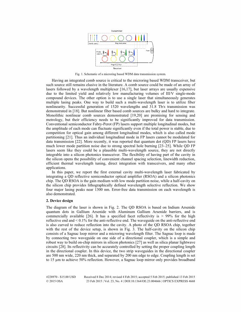
Fig. 1. Schematic of a microring based WDM data transmission system.
Having an integrated comb source is critical to the microring based WDM transceiver, but such source still remains elusive in the literature. A comb source could be made of an array of lasers followed by a wavelength multiplexer [16,17], but laser arrays are usually expensive due to the limited yield and relatively low manufacturing volumes of III/V single-mode compound devices. The other option is to use a single laser that simultaneously generates multiple lasing peaks. One way to build such a multi-wavelength laser is to utilize fiber nonlinearity. Successful generation of 1520 wavelengths and 31.8 Tb/s transmission was demonstrated in [18]. But nonlinear fiber based comb sources are bulky and hard to integrate. Monolithic nonlinear comb sources demonstrated [19,20] are promising for sensing and metrology, but their efficiency needs to be significantly improved for data transmission. Conventional semiconductor Fabry-Perot (FP) lasers support multiple longitudinal modes, but the amplitude of each mode can fluctuate significantly even if the total power is stable, due to competition for optical gain among different longitudinal modes, which is also called mode partitioning [21]. Thus an individual longitudinal mode in FP lasers cannot be modulated for data transmission [22]. More recently, it was reported that quantum dot (QD) FP lasers have much lower mode partition noise due to strong spectral hole burning [23–25]. While QD FP lasers seem like they could be a plausible multi-wavelength source, they are not directly integrable into a silicon photonics transceiver. The flexibility of having part of the cavity in the silicon opens the possibility of convenient channel spacing selection, linewidth reduction, efficient thermal wavelength tuning, direct integration with transceivers, and many other applications.
In this paper, we report the first external cavity multi-wavelength laser fabricated by integrating a QD reflective semiconductor optical amplifier (RSOA) and a silicon photonics chip. The QD RSOA is the gain medium with low mode partition noise, while a half-cavity on the silicon chip provides lithographically defined wavelength selective reflection. We show four major lasing peaks near 1300 nm. Error-free data transmission on each wavelength is also demonstrated.
2. Device design
The diagram of the laser is shown in Fig. 2. The QD RSOA is based on Indium Arsenide quantum dots in Gallium Arsenide with Aluminum Gallium Arsenide barriers, and is commercially available [26]. It has a specified facet reflectivity is > 99% for the high reflective end and < 0.1% for the anti-reflective end. The waveguide on the anti-reflective end is also curved to reduce reflection into the cavity. A photo of the QD RSOA chip, together with the rest of the device setup, is shown in Fig. 3. The half-cavity on the silicon chip consists of a Sagnac loop mirror and a microring wavelength filter. The Sagnac loop is made by connecting two waveguide on one side of a directional coupler, which is a simple and robust way to build on-chip mirrors in silicon photonics [27] as well as silica planar lightwave circuits [28]. Its reflectivity can be accurately controlled by setting the proper coupling length in the directional coupler. In this device, the two strip waveguides in the directional coupler are 500 nm wide, 220 nm thick, and separated by 200 nm edge to edge. Coupling length is set to 15 µm to achieve 50% reflection. However, a Sagnac loop mirror only provides broadband
#228970 - $15.00 USD Received 8 Dec 2014; revised 4 Feb 2015; accepted 5 Feb 2015; published 13 Feb 2015 © 2015 OSA 23 Feb 2015 | Vol. 23, No. 4 | DOI:10.1364/OE.23.004666 | OPTICS EXPRESS 4668

reflection, so a microring wavelength filter is inserted in the cavity for wavelength selection. The ring radius is 35 µm, with 2 µm straight waveguide in coupling region, corresponding to a free spectral range (FSR) of 2 nm. The measured transmission spectrum of this microring filter is shown in black dashed line in Fig. 4. The Y-junction in between the two grating couplers is a well-characterized device [29], and it enables us to measure the grating coupler efficiency using a commercial test laser.
Fig. 2. Diagram of the QD RSOA / silicon hybrid multi-wavelength laser.
To reduce the coupling loss at the RSOA/silicon interface, light in the submicron silicon waveguide is first coupled into a silicon nitride waveguide using an inverse taper. The silicon nitride waveguide is adiabatically tapered wider in the horizontal direction to match the RSOA waveguide width. In the vertical dimension, the nitride waveguide is only 200 nm thick, which leads to a much lower confinement factor and allows the modal field to extend into the oxide cladding to better match the RSOA mode. The designed nitride waveguide mode field diameter is 3.5 µm × 0.7 µm, close to a typical SOA mode size.
3. Device characterization
3.1 Chip alignment
The silicon chip was polished after wafer dicing to create a flat and smooth facet for butt coupling. No anti-reflective coating was applied on the silicon chip. Then both the RSOA and the silicon chip were mounted on six-axis stages for alignment. The RSOA chip was kept at 25 °C using a thermo-electric cooler (TEC), while the silicon chip remained at the ambient temperature of the metal stage. 210 mA of pump current was provided to the RSOA from a DC source during alignment. A lensed fiber coupled to the 0.1% anti-reflective facet was used to monitor the cavity ASE or lasing power as a feedback for active alignment. After the QD RSOA and silicon chip were properly aligned, a fiber array was brought in to capture the output from the grating coupler. An image of the testing setup is shown in Fig. 3, as well as a zoomed-in view of the silicon chip/RSOA interface.
Fig. 3. Image of the alignment setup (left), and a zoomed-in view of the RSOA / silicon chip interface (lower right). A schematic of the grating coupler on chip is shown top right, containing a Y-junction and an additional output coupler to assist fiber array coupling. The fiber array can be seen in the top left of the figure.
#228970 - $15.00 USD Received 8 Dec 2014; revised 4 Feb 2015; accepted 5 Feb 2015; published 13 Feb 2015 © 2015 OSA 23 Feb 2015 | Vol. 23, No. 4 | DOI:10.1364/OE.23.004666 | OPTICS EXPRESS 4669

3.2 Laser spectrum and LIV
The output of the fiber array was connected to an optical spectrum analyzer. The displayed spectrum is plotted in Fig. 4, as well as the intra-cavity microring filter transmission spectrum. Multiple lasing peaks were demonstrated, and the laser mode spacing matches the FSR of the microring filter, which is 2 nm as mentioned earlier. Four major lasing peaks were observed between 1300 nm and 1308 nm, with less than 3 dB power non-uniformity.
Fig. 4. Laser spectrum (solid blue line) and microring filter transmission spectrum (dashed black line).
The laser LIV characteristics are shown in Fig. 5. The blue line shows a typical rectifying IV curve of a p-n diode, and the red line indicates a threshold current of 60 mA. The on-chip output power at 200 mA, about three times the threshold, is 20 mW, corresponding to a wall-plug efficiency (WPE) of 5.9%.
Fig. 5. Laser output power (red) and forward bias voltage (blue) as a function of drive current.
3.3 Data transmission experiment
To validate the viability of the multi-wavelength laser for WDM data communication applications, each laser peak was filtered out using a tunable filter and modulated using a Lithium Niobate Mache-Zehnder modulator. The data stream used for modulation is a 10 Gb/s non-return to zero (NRZ) 27-1 pseudo random bit sequence (PRBS). The modulated optical signal was split into two branches. One branch was amplified using a Praseodymium-doped-fiber-amplifier (PDFA) and displayed on a digital communication analyzer (DCA). The other branch was first connected to a variable optical attenuator, then an avalanche photodetector (APD) and a bit error rate tester (BERT). The eye diagrams from the 4 lasing peaks are shown Fig. 6(a)-6(d), along with the filtered spectrum of one of the peaks Fig. 6(f). Eye diagram of a control experiment conducted using a commercial 1310 nm laser is shown in Fig. 6(e). Open eye diagrams are observed on all four channels, qualitatively confirming
#228970 - $15.00 USD Received 8 Dec 2014; revised 4 Feb 2015; accepted 5 Feb 2015; published 13 Feb 2015 © 2015 OSA 23 Feb 2015 | Vol. 23, No. 4 | DOI:10.1364/OE.23.004666 | OPTICS EXPRESS 4670

successful data transmission. Testing configuration illustrated in Fig. 7(a). Recorded bit error rate (BER) as a function of received power is plotted in Fig. 7(b). At 10−9 bit error rate, all channels have less than 2.6 dB power penalty compared to the commercial laser. We note that the eye diagrams and receiver sensitivity from different channels are slightly non-uniform most likely because the relative position of the RSOA and silicon chip was drifting over the period of the BER measurement. This drift could be eliminated by bonding the RSOA and silicon chips together using epoxy or by upgrading our alignment stages.
Fig. 6. (a)-(d) corresponds to channel 1-4, (e) is control experiment using commercial DFB, and (f) is one filtered spectrum.
Fig. 7. Testing configuration diagram and bit error rate as a function of received power.
4. Conclusion
To conclude, we demonstrate a hybrid external cavity multi-wavelength laser using a QD RSOA and a silicon photonics chip. Four lasing mode at 2 nm spacing and less than 3 dB power non-uniformity were observed, with over 20 mW of total output power. We also show that each lasing peak can be successfully modulated at 10 Gb/s. At 10−9 BER, the receiver power penalty is less than 2.6 dB compared to a commercial laser. This work demonstrates the possibility of using silicon photonics to build a comb laser source for WDM transmission in future optical interconnection systems.
Acknowledgments
The authors would like to thank AT&T for loan of equipment. The authors also thank Dr. Noam Ophir from Coriant Advanced Technology Group for help with testing and useful discussions. We would also like to thank Gernot Pomrenke of AFOSR for his support of the OpSIS effort, through both a PECASE award (FA9550-13-1-0027) and funding for OpSIS (FA9550-10-l-0439). We gratefully acknowledge support from AFOSR STTR grants FA9550-12-C-0079. The authors would also like to thank Mentor Graphics and Lumerical for their support of the OpSIS project.
#228970 - $15.00 USD Received 8 Dec 2014; revised 4 Feb 2015; accepted 5 Feb 2015; published 13 Feb 2015 © 2015 OSA 23 Feb 2015 | Vol. 23, No. 4 | DOI:10.1364/OE.23.004666 | OPTICS EXPRESS 4671