Quantum Dot Photonic Crystal Light Sources
14
Quantum Dot Photonic Crystal Light Sources PALLAB BHATTACHARYA, FELLOW, IEEE, JAYSHRI SABARINATHAN, MEMBER, IEEE, JURAJ TOPOL’AN ˇ CIK, SWAPNAJIT CHAKRAVARTY, PEI-CHEN YU, AND WEIDONG ZHOU, MEMBER, IEEE Invited Paper The control and manipulation of light on a planar IC similar to that achieved for electrons in semiconductor chips on submicrom- eter and nanometer scales is an area of very active research today. While electronic device miniaturization is close to reaching its max- imum possible potential, photonic devices have unique properties that have yet to be exploited. With increasing advances in nanofab- rication techniques and the understanding of optical properties of semiconductors, several optical devices such as lasers, detectors, interferometers, and waveguides have been constantly shrinking in size. We have achieved very high speed integrated optical devices at 10–100- m length scales. However, there is a need to further re- duce the size of devices to make them competitive in size and cost to existing electronic devices and to utilize their potential and unique properties in a wide range of applications ranging from communi- cations, displays to sensors. Photonic crystals have emerged as one of the best potential candidates that can achieve the goal of compact miniaturized photonic chips. In this paper, we describe the current efforts and advances made in the photonic crystal microcavity light sources and their future prospects. Keywords—Edge-emitting device, electrically injected, en- hanced spontaneous emission, integrated optoelectronics, micro- cavity laser, photonic bandgap (PBG), photonic crystal (PC), Purcell effect, quality factor, quantum dots (QDs), quantum well heterostructure, stimulated emission, surface-emitting light source, waveguide. I. INTRODUCTION The vision of miniaturized photonic devices, which function in a wide range of applications such as portable Manuscript received March 8, 2005; revised March 15, 2005. This work was supported in part by the Army Research Office (ARO), in part by the Office of Naval Research (ONR), and in part by the Defense Advanced Re- search Projects Agency (DARPA). P. Bhattacharya, J. Topol’anˇ cik, S. Chakravarty and P.-C. Yu are with the Solid State Electronics Laboratory, Department of Electrical Engineering and Computer Science, University of Michigan, Ann Arbor, MI 48109-2122 USA (e-mail: [email protected]). J. Sabarinathan is with the Department of Electrical and Computer Engi- neering, University of Western Ontario, London, ON N6A 5B9, Canada. W. Zhou is with the Department of Electrical Engineering, University of Texas at Arlington, Arlington, TX 76019-0016 USA. Digital Object Identifier 10.1109/JPROC.2005.853555 environmental sensors to detect hazardous compounds or to sample and analyze nanoscopic volumes of biological fluids with high speed, accuracy, and cost effectiveness, or ultracompact low-cost high-speed communication devices, will be realized only when we can sufficiently manipulate light (photons) on the submicrometer scale similar to what has been achieved for electrons in semiconductor devices. Photonic crystals (PCs)—or photonic bandgap (PBG) struc- tures, as they are also called [1]–[3]—have emerged as feasible solutions to answer this need for a wide range of devices including single-photon sources, lasers, detectors, filters, waveguides, sensors, and optical interconnects. They provide both unique optical properties as well as great flexibility in the design, fabrication, and integration of these devices in various configurations as required for diverse photonic and optoelectronic applications. PCs in the optical regime are periodic dielectric structures with variations in the refractive index on length scales of the order of the wavelength of light (a few hundred microme- ters). Bragg diffraction in these periodic arrangements results in light interference manifested in photonic bandgaps, where propagation of certain frequencies of electromagnetic radia- tion is inhibited [see Fig. 1(a)]. Introducing point and line defects in the periodic photonic lattices give rise to local- ized modes within the bandgaps and hence allow us to con- fine and manipulate the flow of light in these structures. This behavior is analogous to that seen in crystalline semicon- ductors thereby making PCs excellent candidates for PBG and defect engineering. Since PCs were first described by Yablonovitch [1] and John [2] in 1987, extensive advances in micro- and nanofabrication have allowed us to construct PCs with bandgaps in the optical regime. PC structures with their multiparameter design flexibility have been the subject of intense research and development over the past decade. The recent notable contributions of PCs to improvement of the existing conventional semi- conductor light sources include, for example, replacement of the cleaved laser facets with PCs [4], enhancement of vertical extraction efficiency in LEDs [5], reduction of refractive index in vertical cavity surface-emitting lasers 0018-9219/$20.00 © 2005 IEEE PROCEEDINGS OF THE IEEE, VOL. 93, NO. 10, OCTOBER 2005 1825
Transcript of Quantum Dot Photonic Crystal Light Sources
Quantum Dot Photonic Crystal Light Sources
PALLAB BHATTACHARYA, FELLOW, IEEE, JAYSHRI SABARINATHAN, MEMBER, IEEE,JURAJ TOPOL’ANCIK, SWAPNAJIT CHAKRAVARTY, PEI-CHEN YU, AND
WEIDONG ZHOU, MEMBER, IEEE
Invited Paper
The control and manipulation of light on a planar IC similar tothat achieved for electrons in semiconductor chips on submicrom-eter and nanometer scales is an area of very active research today.While electronic device miniaturization is close to reaching its max-imum possible potential, photonic devices have unique propertiesthat have yet to be exploited. With increasing advances in nanofab-rication techniques and the understanding of optical properties ofsemiconductors, several optical devices such as lasers, detectors,interferometers, and waveguides have been constantly shrinking insize. We have achieved very high speed integrated optical devicesat 10–100-�m length scales. However, there is a need to further re-duce the size of devices to make them competitive in size and cost toexisting electronic devices and to utilize their potential and uniqueproperties in a wide range of applications ranging from communi-cations, displays to sensors. Photonic crystals have emerged as oneof the best potential candidates that can achieve the goal of compactminiaturized photonic chips. In this paper, we describe the currentefforts and advances made in the photonic crystal microcavity lightsources and their future prospects.
Keywords—Edge-emitting device, electrically injected, en-hanced spontaneous emission, integrated optoelectronics, micro-cavity laser, photonic bandgap (PBG), photonic crystal (PC),Purcell effect, quality factor, quantum dots (QDs), quantum wellheterostructure, stimulated emission, surface-emitting light source,waveguide.
I. INTRODUCTION
The vision of miniaturized photonic devices, whichfunction in a wide range of applications such as portable
Manuscript received March 8, 2005; revised March 15, 2005. This workwas supported in part by the Army Research Office (ARO), in part by theOffice of Naval Research (ONR), and in part by the Defense Advanced Re-search Projects Agency (DARPA).
P. Bhattacharya, J. Topol’ancik, S. Chakravarty and P.-C. Yu are with theSolid State Electronics Laboratory, Department of Electrical Engineeringand Computer Science, University of Michigan, Ann Arbor, MI 48109-2122USA (e-mail: [email protected]).
J. Sabarinathan is with the Department of Electrical and Computer Engi-neering, University of Western Ontario, London, ON N6A 5B9, Canada.
W. Zhou is with the Department of Electrical Engineering, University ofTexas at Arlington, Arlington, TX 76019-0016 USA.
Digital Object Identifier 10.1109/JPROC.2005.853555
environmental sensors to detect hazardous compounds orto sample and analyze nanoscopic volumes of biologicalfluids with high speed, accuracy, and cost effectiveness, orultracompact low-cost high-speed communication devices,will be realized only when we can sufficiently manipulatelight (photons) on the submicrometer scale similar to whathas been achieved for electrons in semiconductor devices.Photonic crystals (PCs)—or photonic bandgap (PBG) struc-tures, as they are also called [1]–[3]—have emerged asfeasible solutions to answer this need for a wide range ofdevices including single-photon sources, lasers, detectors,filters, waveguides, sensors, and optical interconnects. Theyprovide both unique optical properties as well as greatflexibility in the design, fabrication, and integration of thesedevices in various configurations as required for diversephotonic and optoelectronic applications.
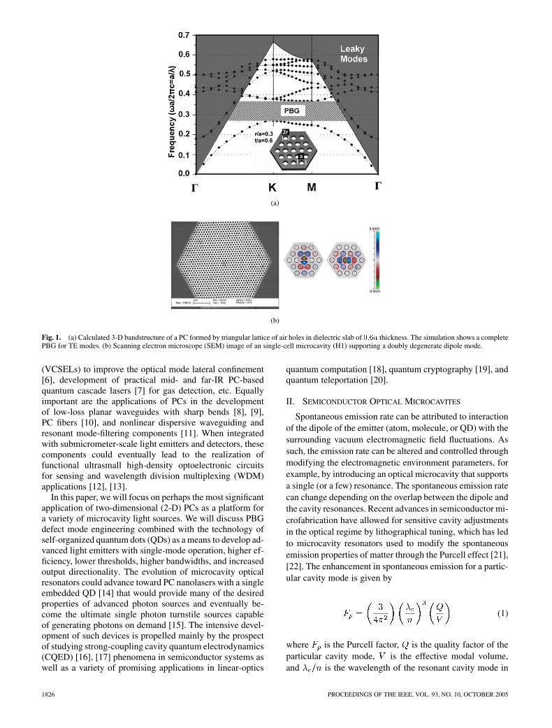
PCs in the optical regime are periodic dielectric structureswith variations in the refractive index on length scales of theorder of the wavelength of light (a few hundred microme-ters). Bragg diffraction in these periodic arrangements resultsin light interference manifested in photonic bandgaps, wherepropagation of certain frequencies of electromagnetic radia-tion is inhibited [see Fig. 1(a)]. Introducing point and linedefects in the periodic photonic lattices give rise to local-ized modes within the bandgaps and hence allow us to con-fine and manipulate the flow of light in these structures. Thisbehavior is analogous to that seen in crystalline semicon-ductors thereby making PCs excellent candidates for PBGand defect engineering. Since PCs were first described byYablonovitch [1] and John [2] in 1987, extensive advancesin micro- and nanofabrication have allowed us to constructPCs with bandgaps in the optical regime.
PC structures with their multiparameter design flexibilityhave been the subject of intense research and developmentover the past decade. The recent notable contributions ofPCs to improvement of the existing conventional semi-conductor light sources include, for example, replacementof the cleaved laser facets with PCs [4], enhancement ofvertical extraction efficiency in LEDs [5], reduction ofrefractive index in vertical cavity surface-emitting lasers
0018-9219/$20.00 © 2005 IEEE
PROCEEDINGS OF THE IEEE, VOL. 93, NO. 10, OCTOBER 2005 1825
(a)
(b)
Fig. 1. (a) Calculated 3-D bandstructure of a PC formed by triangular lattice of air holes in dielectric slab of 0:6a thickness. The simulation shows a completePBG for TE modes. (b) Scanning electron microscope (SEM) image of an single-cell microcavity (H1) supporting a doubly degenerate dipole mode.
(VCSELs) to improve the optical mode lateral confinement[6], development of practical mid- and far-IR PC-basedquantum cascade lasers [7] for gas detection, etc. Equallyimportant are the applications of PCs in the developmentof low-loss planar waveguides with sharp bends [8], [9],PC fibers [10], and nonlinear dispersive waveguiding andresonant mode-filtering components [11]. When integratedwith submicrometer-scale light emitters and detectors, thesecomponents could eventually lead to the realization offunctional ultrasmall high-density optoelectronic circuitsfor sensing and wavelength division multiplexing (WDM)applications [12], [13].
In this paper, we will focus on perhaps the most significantapplication of two-dimensional (2-D) PCs as a platform fora variety of microcavity light sources. We will discuss PBGdefect mode engineering combined with the technology ofself-organized quantum dots (QDs) as a means to develop ad-vanced light emitters with single-mode operation, higher ef-ficiency, lower thresholds, higher bandwidths, and increasedoutput directionality. The evolution of microcavity opticalresonators could advance toward PC nanolasers with a singleembedded QD [14] that would provide many of the desiredproperties of advanced photon sources and eventually be-come the ultimate single photon turnstile sources capableof generating photons on demand [15]. The intensive devel-opment of such devices is propelled mainly by the prospectof studying strong-coupling cavity quantum electrodynamics(CQED) [16], [17] phenomena in semiconductor systems aswell as a variety of promising applications in linear-optics
quantum computation [18], quantum cryptography [19], andquantum teleportation [20].
II. SEMICONDUCTOR OPTICAL MICROCAVITES
Spontaneous emission rate can be attributed to interactionof the dipole of the emitter (atom, molecule, or QD) with thesurrounding vacuum electromagnetic field fluctuations. Assuch, the emission rate can be altered and controlled throughmodifying the electromagnetic environment parameters, forexample, by introducing an optical microcavity that supportsa single (or a few) resonance. The spontaneous emission ratecan change depending on the overlap between the dipole andthe cavity resonances. Recent advances in semiconductor mi-crofabrication have allowed for sensitive cavity adjustmentsin the optical regime by lithographical tuning, which has ledto microcavity resonators used to modify the spontaneousemission properties of matter through the Purcell effect [21],[22]. The enhancement in spontaneous emission for a partic-ular cavity mode is given by
(1)
where is the Purcell factor, is the quality factor of theparticular cavity mode, is the effective modal volume,and is the wavelength of the resonant cavity mode in
1826 PROCEEDINGS OF THE IEEE, VOL. 93, NO. 10, OCTOBER 2005
the medium with refractive index . The Purcell factor hasbecome a very useful figure of merit for a microcavity andin determining the strength of the cavity–emitter interac-tion. The development of optical microcavities is thereforedriven by the desire to obtain the highest possible and thesmallest possible modal volume for maximum enhance-ment of light–matter interaction.
Several types of semiconductor optical microcavities in-cluding silica microspheres [23], toroid microcavities [24],microdisks [25]–[27], micropillar resonators [28], [29],Fabry–Pérot resonators [30], and cylindrical and oxide-con-fined microcavities [31] with various emission sources in thecavity have been investigated to study single-photon gen-eration [24], strong- [23], [24] and weak-coupling CQED[25]–[29], and spontaneous emission enhancement (sup-pression) phenomena [23]–[27]. Excellent comprehensivereviews of optical microcavities in the context of CQED areavailable [32]–[35].
Strong-coupling phenomena in optical microcavitieshave been observed by Hood et al. on cesium atomsstrongly coupled to electromagnetic fields in an ultrahigh-Fabry–Pérot cavity [30]. Experimentally demonstrated ul-trahigh factors of microspheres 8 10 [23] andtoroid microcavities 10 [24] make these structurespotential candidates for CQED experiments. Alternativeversions of semiconductor optical microresonators such asmicropillars have so far failed to deliver sufficiently highvalues for CQED, but have found an important applicationin triggered single-photon sources [28], [29], [36]. Sincethe idea was proposed by Gérard et al. [37], QDs withtheir atom-like density of states have gradually become thepreferred emitter used in the more recent demonstrations,since, unlike neutral atoms, QDs can be confined in thehigh field density regions within the semiconductors. Thedemonstrated semiconductor single mode micropost deviceswith an embedded QD provide experimental evidence ofweak coupling [28], [29] and up to 32-fold enhancementin spontaneous emission [38]. These results present severalpractical advantages such as single mode operation, narrowemission linewidth, lower (and potentially zero) thresholdlasing, and higher collection efficiency when microcavityresonators are used as light emitters. The major challengein obtaining high microcavities in the optical regimewith the above techniques is that radiative losses increasewith decreasing volume of the cavity. Such microcavitiesalso routinely suffer from losses at the surfaces (hence lower
). Furthermore, when the horizontal width of the cavityis reduced to approximately 1–2 m (i.e., as the volumeis reduced), the cavity varies widely even with slightgeometry variations, and it is difficult to obtain repeatableperformance. Finally, these techniques offer limited flexi-bility in designing the cavity mode profiles.
PC-based optical cavities have numerous advantagesincluding superior mechanical stability, relaxed fabricationtolerances, and possibility of electrical excitation, over theabove devices and have emerged as the preferred technology
for building microcavity light sources. Optically pumpedPCs have been used successfully to control the spontaneousemission rate of QDs [39], [40]. Several single-cell micro-cavity designs [41], [42] with sufficiently large theoretical
values for QED experiments have been proposed, buthave not yet been successfully fabricated and experimentallydemonstrated. The recent report by Englund et al. [43] onthe observation of fivefold enhancement of spontaneousemission rate of QDs placed in an optimized high- 2-DPC microcavity represents the first experimental demonstra-tion of on demand single photon emission from an opticalmicroresonator. Techniques are currently being developedto obtain a single InAs/InP self-assembled QD in a chosenlocation on the substrate [44] or position the PC cavities tosingle InAs QDs [45]. Further advances which incorporatesuch a single QD into a PC microcavity can be used tocreate single-photon sources for studying CQED processesin semiconductor systems such as strongly coupled dots andsingle dot lasing.
III. SELF-ASSEMBLED SEMICONDUCTOR QDS
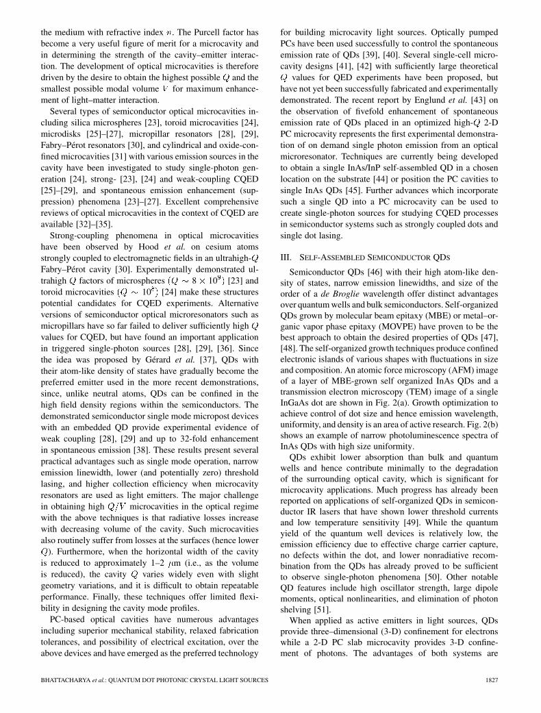
Semiconductor QDs [46] with their high atom-like den-sity of states, narrow emission linewidths, and size of theorder of a de Broglie wavelength offer distinct advantagesover quantum wells and bulk semiconductors. Self-organizedQDs grown by molecular beam epitaxy (MBE) or metal–or-ganic vapor phase epitaxy (MOVPE) have proven to be thebest approach to obtain the desired properties of QDs [47],[48]. The self-organized growth techniques produce confinedelectronic islands of various shapes with fluctuations in sizeand composition. An atomic force microscopy (AFM) imageof a layer of MBE-grown self organized InAs QDs and atransmission electron microscopy (TEM) image of a singleInGaAs dot are shown in Fig. 2(a). Growth optimization toachieve control of dot size and hence emission wavelength,uniformity, and density is an area of active research. Fig. 2(b)shows an example of narrow photoluminescence spectra ofInAs QDs with high size uniformity.
QDs exhibit lower absorption than bulk and quantumwells and hence contribute minimally to the degradationof the surrounding optical cavity, which is significant formicrocavity applications. Much progress has already beenreported on applications of self-organized QDs in semicon-ductor IR lasers that have shown lower threshold currentsand low temperature sensitivity [49]. While the quantumyield of the quantum well devices is relatively low, theemission efficiency due to effective charge carrier capture,no defects within the dot, and lower nonradiative recom-bination from the QDs has already proved to be sufficientto observe single-photon phenomena [50]. Other notableQD features include high oscillator strength, large dipolemoments, optical nonlinearities, and elimination of photonshelving [51].
When applied as active emitters in light sources, QDsprovide three–dimensional (3-D) confinement for electronswhile a 2-D PC slab microcavity provides 3-D confine-ment of photons. The advantages of both systems are
BHATTACHARYA et al.: QUANTUM DOT PHOTONIC CRYSTAL LIGHT SOURCES 1827
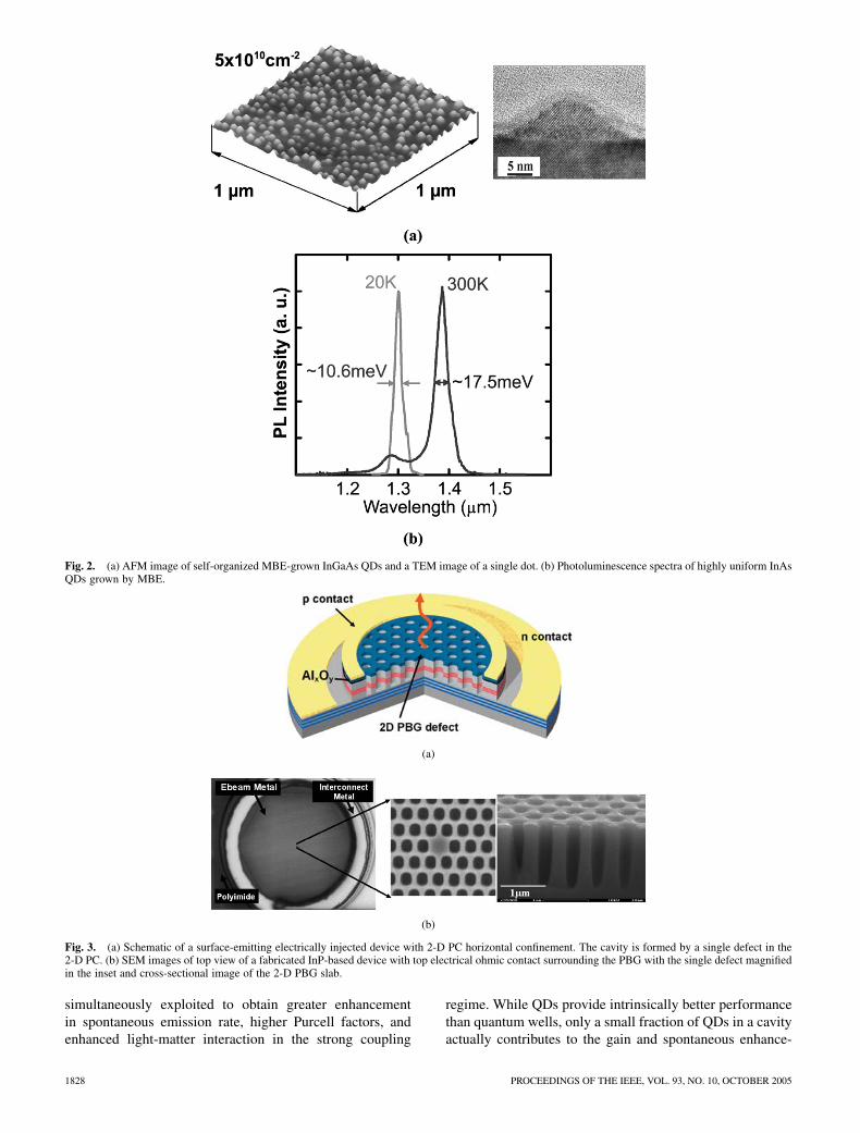
Fig. 2. (a) AFM image of self-organized MBE-grown InGaAs QDs and a TEM image of a single dot. (b) Photoluminescence spectra of highly uniform InAsQDs grown by MBE.
(a)
(b)
Fig. 3. (a) Schematic of a surface-emitting electrically injected device with 2-D PC horizontal confinement. The cavity is formed by a single defect in the2-D PC. (b) SEM images of top view of a fabricated InP-based device with top electrical ohmic contact surrounding the PBG with the single defect magnifiedin the inset and cross-sectional image of the 2-D PBG slab.
simultaneously exploited to obtain greater enhancementin spontaneous emission rate, higher Purcell factors, andenhanced light-matter interaction in the strong coupling
regime. While QDs provide intrinsically better performancethan quantum wells, only a small fraction of QDs in a cavityactually contributes to the gain and spontaneous enhance-
1828 PROCEEDINGS OF THE IEEE, VOL. 93, NO. 10, OCTOBER 2005
ment as the cavity is increased. A better control of thesize, position, and number of QDs and higher cavities areneeded to achieve the maximum potential of this system.
IV. OPTICALLY PUMPED PC MICROCAVITIES
There are two methods of achieving excitation of theactive material inside the cavity—optical pumping and elec-trical injection. Devices requiring optical pumping requirerelatively simple heterostructure design, are easier to fabri-cate, and provide clear comparisons with theoretical modesimulations. Two-dimensional PCs formed of a triangularlattice of air-holes in free-standing semiconductor slabs[52]–[54] have become most popular systems used to studyPC microcavity effects due to their ability to accommodatean appropriate photoluminescent material within the highfield regions. By selectively removing one or more air-holesand thereby introducing a defect mode(s) in a 2-D photoniclattice, or modifying the region near the cavity, a microcavitywith a wide range of tailored modes excitable by the activematerial within the cavity can be created. Although thesestructures provide only quasi-3-D light confinement withthe horizontal confinement provided by the PBG and thevertical confinement by total internal reflection provided bythe cladding (air, oxide, or DBR), they are rather capable ofconfining light within small cavities with significantly high
factors.Ideally, a 3-D PC with a defect microcavity formed by a
missing period in the lattice would provide the best confine-ment for a light emitter placed inside the cavity, due to thePBG confinement in all spatial dimensions. While there areinteresting results on 3-D PCs in different material systems[55], it is practically difficult to fabricate cavities with suffi-ciently high in semiconductor-based 3-D PCs and, at thesame time, incorporate a suitable active emitter within thosecavities.
Two-dimensional PC defect microcavities can provideboth sufficiently high as well as ultrasmall modal vol-umes ( ) and hence a very high ratio—a necessarycondition for achieving a high spontaneous emission rateenhancement. The quasi-3-D nature of these structuresallows for mode coupling to the radiated modes in the ver-tical direction, which establishes a significant radiation lossmechanism and reduction in the cavities. A simple cavityin triangular lattice formed by removing one air-hole sup-ports doubly degenerate dipole modes with a rather modest
of a few hundreds. The can be improved by splitting themode degeneracy by modifying the size or position of the PCholes around the cavity. Extensive numerical design workusing 3-D finite-difference time-domain (FDTD) simulationtools performed by Scherer et al. at Caltech led to optimizedsingle cell cavity designs in air-clad semiconductor slabswith large ( ) factors [41], [56], [57]. These and similarstudies performed by other groups involved the optimizationof the slab thickness [58], and modification of sizes and ge-ometries of cavities embedded in both square and triangularlattice PCs [59], [60]. It should be noted that such flexibilityin designing the geometry of optical microcavities is onlyoffered by PCs. Similar work performed by Noda et al.
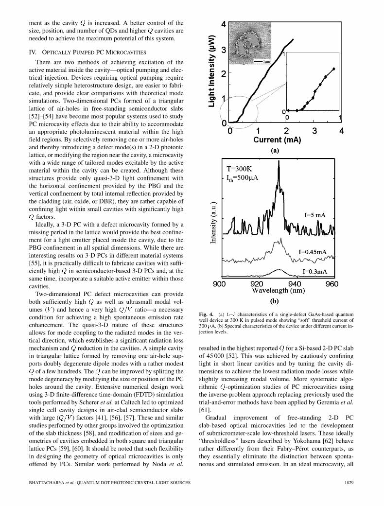
Fig. 4. (a) L–I characteristics of a single-defect GaAs-based quantumwell device at 300 K in pulsed mode showing “soft” threshold current of300 �A. (b) Spectral characteristics of the device under different current in-jection levels.
resulted in the highest reported for a Si-based 2-D PC slabof 45 000 [52]. This was achieved by cautiously confininglight in short linear cavities and by tuning the cavity di-mensions to achieve the lowest radiation mode losses whileslightly increasing modal volume. More systematic algo-rithmic -optimization studies of PC microcavities usingthe inverse-problem approach replacing previously used thetrial-and-error methods have been applied by Geremia et al.[61].
Gradual improvement of free-standing 2-D PCslab-based optical microcavities led to the developmentof submicrometer-scale low-threshold lasers. These ideally“thresholdless” lasers described by Yokohama [62] behaverather differently from their Fabry–Pérot counterparts, asthey essentially eliminate the distinction between sponta-neous and stimulated emission. In an ideal microcavity, all
BHATTACHARYA et al.: QUANTUM DOT PHOTONIC CRYSTAL LIGHT SOURCES 1829
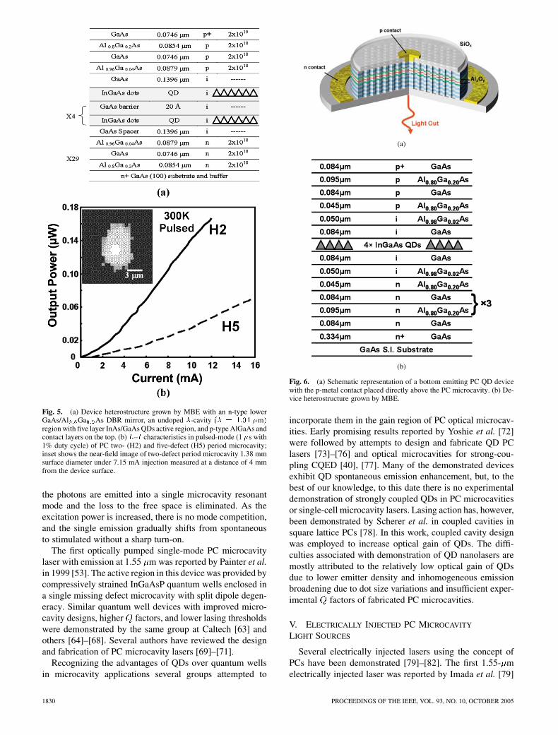
Fig. 5. (a) Device heterostructure grown by MBE with an n-type lowerGaAs/Al Ga As DBR mirror, an undoped �-cavity (� = 1:04 �m)region with five layer InAs/GaAs QDs active region, and p-type AlGaAs andcontact layers on the top. (b) L–I characteristics in pulsed-mode (1 �s with1% duty cycle) of PC two- (H2) and five-defect (H5) period microcavity;inset shows the near-field image of two-defect period microcavity 1.38 mmsurface diameter under 7.15 mA injection measured at a distance of 4 mmfrom the device surface.
the photons are emitted into a single microcavity resonantmode and the loss to the free space is eliminated. As theexcitation power is increased, there is no mode competition,and the single emission gradually shifts from spontaneousto stimulated without a sharp turn-on.
The first optically pumped single-mode PC microcavitylaser with emission at 1.55 m was reported by Painter et al.in 1999 [53]. The active region in this device was provided bycompressively strained InGaAsP quantum wells enclosed ina single missing defect microcavity with split dipole degen-eracy. Similar quantum well devices with improved micro-cavity designs, higher factors, and lower lasing thresholdswere demonstrated by the same group at Caltech [63] andothers [64]–[68]. Several authors have reviewed the designand fabrication of PC microcavity lasers [69]–[71].
Recognizing the advantages of QDs over quantum wellsin microcavity applications several groups attempted to
(a)
(b)
Fig. 6. (a) Schematic representation of a bottom emitting PC QD devicewith the p-metal contact placed directly above the PC microcavity. (b) De-vice heterostructure grown by MBE.
incorporate them in the gain region of PC optical microcav-ities. Early promising results reported by Yoshie et al. [72]were followed by attempts to design and fabricate QD PClasers [73]–[76] and optical microcavities for strong-cou-pling CQED [40], [77]. Many of the demonstrated devicesexhibit QD spontaneous emission enhancement, but, to thebest of our knowledge, to this date there is no experimentaldemonstration of strongly coupled QDs in PC microcavitiesor single-cell microcavity lasers. Lasing action has, however,been demonstrated by Scherer et al. in coupled cavities insquare lattice PCs [78]. In this work, coupled cavity designwas employed to increase optical gain of QDs. The diffi-culties associated with demonstration of QD nanolasers aremostly attributed to the relatively low optical gain of QDsdue to lower emitter density and inhomogeneous emissionbroadening due to dot size variations and insufficient exper-imental factors of fabricated PC microcavities.
V. ELECTRICALLY INJECTED PC MICROCAVITY
LIGHT SOURCES
Several electrically injected lasers using the concept ofPCs have been demonstrated [79]–[82]. The first 1.55- melectrically injected laser was reported by Imada et al. [79]
1830 PROCEEDINGS OF THE IEEE, VOL. 93, NO. 10, OCTOBER 2005
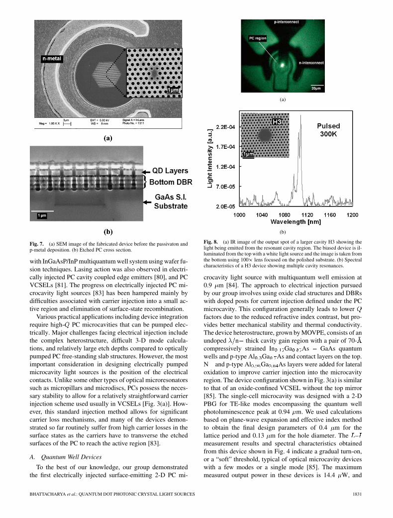
Fig. 7. (a) SEM image of the fabricated device before the passivaton andp-metal deposition. (b) Etched PC cross section.
with InGaAsP/InP multiquantum well system using wafer fu-sion techniques. Lasing action was also observed in electri-cally injected PC cavity coupled edge emitters [80], and PCVCSELs [81]. The progress on electrically injected PC mi-crocavity light sources [83] has been hampered mainly bydifficulties associated with carrier injection into a small ac-tive region and elimination of surface-state recombination.
Various practical applications including device integrationrequire high- PC microcavities that can be pumped elec-trically. Major challenges facing electrical injection includethe complex heterostructure, difficult 3-D mode calcula-tions, and relatively large etch depths compared to opticallypumped PC free-standing slab structures. However, the mostimportant consideration in designing electrically pumpedmicrocavity light sources is the position of the electricalcontacts. Unlike some other types of optical microresonatorssuch as micropillars and microdiscs, PCs possess the neces-sary stability to allow for a relatively straightforward carrierinjection scheme used usually in VCSELs [Fig. 3(a)]. How-ever, this standard injection method allows for significantcarrier loss mechanisms, and many of the devices demon-strated so far routinely suffer from high carrier losses in thesurface states as the carriers have to transverse the etchedsurfaces of the PC to reach the active region [83].
A. Quantum Well Devices
To the best of our knowledge, our group demonstratedthe first electrically injected surface-emitting 2-D PC mi-
(a)
(b)
Fig. 8. (a) IR image of the output spot of a larger cavity H3 showing thelight being emitted from the resonant cavity region. The biased device is il-luminated from the top with a white light source and the image is taken fromthe bottom using 100� lens focused on the polished substrate. (b) Spectralcharacteristics of a H3 device showing multiple cavity resonances.
crocavity light source with multiquantum well emission at0.9 m [84]. The approach to electrical injection pursuedby our group involves using oxide clad structures and DBRswith doped posts for current injection defined under the PCmicrocavity. This configuration generally leads to lowerfactors due to the reduced refractive index contrast, but pro-vides better mechanical stability and thermal conductivity.The device heterostructure, grown by MOVPE, consists of anundoped n thick cavity gain region with a pair of 70-compressively strained In Ga As GaAs quantumwells and p-type Al Ga As and contact layers on the top.N and p-type Al Ga As layers were added for lateraloxidation to improve carrier injection into the microcavityregion. The device configuration shown in Fig. 3(a) is similarto that of an oxide-confined VCSEL without the top mirror[85]. The single-cell microcavity was designed with a 2-DPBG for TE-like modes encompassing the quantum wellphotoluminescence peak at 0.94 m. We used calculationsbased on plane-wave expansion and effective index methodto obtain the final design parameters of 0.4 m for thelattice period and 0.13 m for the hole diameter. The –measurement results and spectral characteristics obtainedfrom this device shown in Fig. 4 indicate a gradual turn-on,or a “soft” threshold, typical of optical microcavity deviceswith a few modes or a single mode [85]. The maximummeasured output power in these devices is 14.4 W, and
BHATTACHARYA et al.: QUANTUM DOT PHOTONIC CRYSTAL LIGHT SOURCES 1831
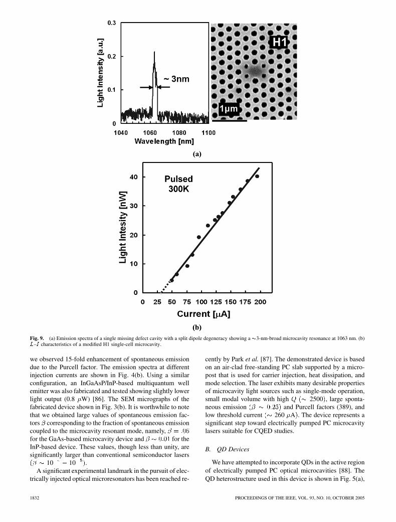
Fig. 9. (a) Emission spectra of a single missing defect cavity with a split dipole degeneracy showing a�3-nm-broad microcavity resonance at 1063 nm. (b)L–I characteristics of a modified H1 single-cell microcavity.
we observed 15-fold enhancement of spontaneous emissiondue to the Purcell factor. The emission spectra at differentinjection currents are shown in Fig. 4(b). Using a similarconfiguration, an InGaAsP/InP-based multiquantum wellemitter was also fabricated and tested showing slightly lowerlight output (0.8 W) [86]. The SEM micrographs of thefabricated device shown in Fig. 3(b). It is worthwhile to notethat we obtained large values of spontaneous emission fac-tors corresponding to the fraction of spontaneous emissioncoupled to the microcavity resonant mode, namely,for the GaAs-based microcavity device and for theInP-based device. These values, though less than unity, aresignificantly larger than conventional semiconductor lasers
10 10 .A significant experimental landmark in the pursuit of elec-
trically injected optical microresonators has been reached re-
cently by Park et al. [87]. The demonstrated device is basedon an air-clad free-standing PC slab supported by a micro-post that is used for carrier injection, heat dissipation, andmode selection. The laser exhibits many desirable propertiesof microcavity light sources such as single-mode operation,small modal volume with high 2500 , large sponta-neous emission and Purcell factors (389), andlow threshold current 260 A . The device represents asignificant step toward electrically pumped PC microcavitylasers suitable for CQED studies.
B. QD Devices
We have attempted to incorporate QDs in the active regionof electrically pumped PC optical microcavities [88]. TheQD heterostructure used in this device is shown in Fig. 5(a),
1832 PROCEEDINGS OF THE IEEE, VOL. 93, NO. 10, OCTOBER 2005
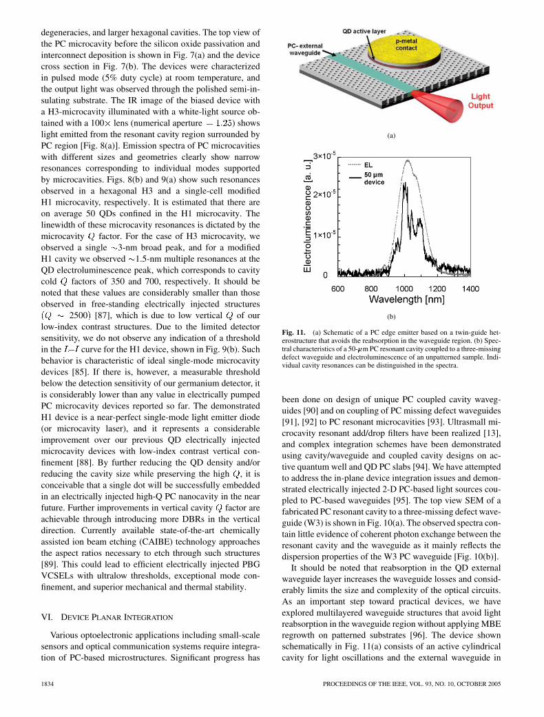
Fig. 10. (a) SEM image of the fabricated PC 6 �m cavity device (H15) coupled to a three-missing defect waveguide. (b) Measured spectral characteristicsshowing spontaneous emission coupled to the waveguide.
and the device schematic is similar to quantum well emit-ters discussed in Section V-A. The PBG in normalized fre-quency range is between 0.39 and 0.43. The normalizedfrequency at mid-gap is chosen for our designencompassing the peak emission of the QDs at mand fill factor . The final design values for the PCwith a hexagonal unit cell are m and m.QDs offer a significantly lower gain when compared withquantum wells, which results in significantly lower outputpowers 0.17 W even from larger multicell cavities H2.It is estimated that there are 500 dots in the PC microcavity.Due to extremely low output power from these devices, wewere unable to study output spectral characteristics, but wedid observe a consistent increase of light output as the cavitysize decreases, which we attributed to improved output direc-tionality due to microcavity effects. The – characteristicsof H2 and H5 hexagonal microcavities are shown in Fig. 5(b).The near-field image of the output, shown in the inset, con-firms photon emission from the PC microcavity and not thepatterned area around it.
Placing the p-metal contact directly above the PC micro-cavity presents a promising way of improving the carrierinjection efficiency of PC emitters. We have attempted to ad-dress this issue with a bottom emitting device with oxide cladactive region and additional pairs of GaAs/Al Ga AsDBRs above and below the active region for improvedvertical mode confinement is shown in the device schematicand QD heterostructure in Fig. 6(a) and (b), respectively.Although considerably degrading the factors of resonantmodes, this method provides superior stability and thermalconductivity to the alternative free standing structures [87].The oxide cladding that improves both carrier and opticalmode confinement is created by selective wet oxidation of85 nm Al Ga As layers surrounding the active GaAsregion with embedded QDs. The PC pattern defined by elec-tron beam lithography was transferred on a silicon nitridemask that served as an etch mask for the deep GaAs elec-tron cyclotron resonance (ECR) reactive ion etch. We haveinvestigated microcavities of various sizes and geometriessuch as short linear cavities, single-cell cavities with split
BHATTACHARYA et al.: QUANTUM DOT PHOTONIC CRYSTAL LIGHT SOURCES 1833
degeneracies, and larger hexagonal cavities. The top view ofthe PC microcavity before the silicon oxide passivation andinterconnect deposition is shown in Fig. 7(a) and the devicecross section in Fig. 7(b). The devices were characterizedin pulsed mode (5% duty cycle) at room temperature, andthe output light was observed through the polished semi-in-sulating substrate. The IR image of the biased device witha H3-microcavity illuminated with a white-light source ob-tained with a 100 lens (numerical aperture ) showslight emitted from the resonant cavity region surrounded byPC region [Fig. 8(a)]. Emission spectra of PC microcavitieswith different sizes and geometries clearly show narrowresonances corresponding to individual modes supportedby microcavities. Figs. 8(b) and 9(a) show such resonancesobserved in a hexagonal H3 and a single-cell modifiedH1 microcavity, respectively. It is estimated that there areon average 50 QDs confined in the H1 microcavity. Thelinewidth of these microcavity resonances is dictated by themicrocavity factor. For the case of H3 microcavity, weobserved a single 3-nm broad peak, and for a modifiedH1 cavity we observed 1.5-nm multiple resonances at theQD electroluminescence peak, which corresponds to cavitycold factors of 350 and 700, respectively. It should benoted that these values are considerably smaller than thoseobserved in free-standing electrically injected structures
2500 [87], which is due to low vertical of ourlow-index contrast structures. Due to the limited detectorsensitivity, we do not observe any indication of a thresholdin the – curve for the H1 device, shown in Fig. 9(b). Suchbehavior is characteristic of ideal single-mode microcavitydevices [85]. If there is, however, a measurable thresholdbelow the detection sensitivity of our germanium detector, itis considerably lower than any value in electrically pumpedPC microcavity devices reported so far. The demonstratedH1 device is a near-perfect single-mode light emitter diode(or microcavity laser), and it represents a considerableimprovement over our previous QD electrically injectedmicrocavity devices with low-index contrast vertical con-finement [88]. By further reducing the QD density and/orreducing the cavity size while preserving the high , it isconceivable that a single dot will be successfully embeddedin an electrically injected high-Q PC nanocavity in the nearfuture. Further improvements in vertical cavity factor areachievable through introducing more DBRs in the verticaldirection. Currently available state-of-the-art chemicallyassisted ion beam etching (CAIBE) technology approachesthe aspect ratios necessary to etch through such structures[89]. This could lead to efficient electrically injected PBGVCSELs with ultralow thresholds, exceptional mode con-finement, and superior mechanical and thermal stability.
VI. DEVICE PLANAR INTEGRATION
Various optoelectronic applications including small-scalesensors and optical communication systems require integra-tion of PC-based microstructures. Significant progress has
(a)
(b)
Fig. 11. (a) Schematic of a PC edge emitter based on a twin-guide het-erostructure that avoids the reabsorption in the waveguide region. (b) Spec-tral characteristics of a 50-�m PC resonant cavity coupled to a three-missingdefect waveguide and electroluminescence of an unpatterned sample. Indi-vidual cavity resonances can be distinguished in the spectra.
been done on design of unique PC coupled cavity waveg-uides [90] and on coupling of PC missing defect waveguides[91], [92] to PC resonant microcavities [93]. Ultrasmall mi-crocavity resonant add/drop filters have been realized [13],and complex integration schemes have been demonstratedusing cavity/waveguide and coupled cavity designs on ac-tive quantum well and QD PC slabs [94]. We have attemptedto address the in-plane device integration issues and demon-strated electrically injected 2-D PC-based light sources cou-pled to PC-based waveguides [95]. The top view SEM of afabricated PC resonant cavity to a three-missing defect wave-guide (W3) is shown in Fig. 10(a). The observed spectra con-tain little evidence of coherent photon exchange between theresonant cavity and the waveguide as it mainly reflects thedispersion properties of the W3 PC waveguide [Fig. 10(b)].
It should be noted that reabsorption in the QD externalwaveguide layer increases the waveguide losses and consid-erably limits the size and complexity of the optical circuits.As an important step toward practical devices, we haveexplored multilayered waveguide structures that avoid lightreabsorption in the waveguide region without applying MBEregrowth on patterned substrates [96]. The device shownschematically in Fig. 11(a) consists of an active cylindricalcavity for light oscillations and the external waveguide in
1834 PROCEEDINGS OF THE IEEE, VOL. 93, NO. 10, OCTOBER 2005
which the PC resonant cavity and waveguide are defined.The electroluminescence generated in the QD active regionfirst couples vertically to the external guide layer, whereit excites the PC hexagonal cavity resonant modes. Thesemodes then transversely couple to the adjacent PC-basedwaveguide. The spectral measurements of devices with verti-cally separated active and guided region indicate significantspectral narrowing due to resonant cavity effects. Fig. 11(b)shows output spectra of a 50 m PC resonant cavity coupledto a three-missing defect waveguide. With smaller modevolumes and higher quality factors, the energy exchangebetween the QD spontaneous emission, the stimulated emis-sion mode within the cavity, and the waveguide mode can besignificantly improved. The next step would involve on-chipintegration of a high-efficiency QD PC laser source with PCwaveguides and QD PC photodiodes, which will functionas an ultracompact integrated photonic chip applicable toa wide range of applications from optical communicationsystems to sensors.
VII. SUMMARY
We have given an overview of the advantages of PC-basedmicrocavity optical resonators. Incorporating QDs into thesedevices has been attained with interesting results. With ef-ficient PC-based electrically injected emitters, sensitive andhighly selective photodiodes, and low loss-waveguides andpassive guiding components, integrated optoelectronic cir-cuits are easily envisioned. When the prospect of a singleQD in a high- PC microcavity and even single-dot lasingat room temperature is achieved in the near future, it willopen the way for several novel applications including single-photon sources for quantum information processing and pro-vide an experimental framework for strong coupling CQEDmeasurements in semiconductor systems.
REFERENCES
[1] E. Yablonovitch, “Inhibited spontaneous emission in solid-statephysics and electronics,” Phys. Rev. Lett., vol. 58, pp. 2059–2062,1987.
[2] S. John, “Strong localization of photons in certain disordered di-electric superlattices,” Phys. Rev. Lett., vol. 58, pp. 2486–2489,1987.
[3] J. D. Joannopolous, P. R. Villeneuve, and S. Fan, “Photonic crys-tals: Putting a new twist on light,” Nature, vol. 386, pp. 143–149,1997.
[4] T. D. Happ, A. Markard, M. Kamp, A. Forchel, S. Anand, J.-L.Gentner, and N. Bouadma, “Nanofabrication of two-dimensionalphotonic crystal mirrors for 1.5 �mshort cavity lasers,” J. Vac. Sci.Technol. B, vol. 19, pp. 2775–2778, 2001.
[5] M. Boroditsky, T. F. Krauss, R. Coccioli, R. Vrijen, R. Bhat, andE. Yablonovitch, “Light extraction from optically pumped light-emitting diode by thin-slab photonic crystals,” Appl. Phys. Lett.,vol. 75, pp. 1036–1038, 1999.
[6] A. J. Danner, J. J. Raftery Jr., N. Yokouchi, and K. D. Choquette,“Transverse modes of photonic crystal vertical-cavity lasers,” Appl.Phys. Lett., vol. 84, pp. 1031–1033, 2004.
[7] R. Colombelli, K. Srinivasan, M. Troccoli, O. Painter, C.Gmachl, D. Tennant, A. Sargent, D. Sivco, A. Cho, and F.Capasso, “Quantum cascade surface-emitting photonic crystallaser,” Science, vol. 302, pp. 1374–1377, 2003.
[8] A. Mekis, J. C. Chen, I. Kurland, S. Fan, P. R. Villeneuve, and J.D. Joannopuolos, “High transmission through sharp bends in pho-tonic crystal waveguides,” Phys. Rev. Lett., vol. 77, pp. 3787–3790,1996.
[9] C. J. M. Smith, H. Benisty, S. Olivier, M. Rattier, C. Weisbuch,T. F. Krauss, R. M. De La Rue, R. Houdré, and U. Oesterle,“Low-loss channel waveguides with two-dimensional photoniccrystal boundaries,” Appl. Phys. Lett., vol. 77, pp. 2813–2815,2000.
[10] J. C. Knight, “Photonic crystal fibers,” Nature, vol. 424, pp.847–851, 2003.
[11] Y. Akahane, T. Asano, B.-S. Song, and S. Noda, “Investigationof high-Q channel drop filters using donor type defects in two-di-mensional photonic crystal slabs,” Appl. Phys. Lett., vol. 83, pp.1512–1514, 2003.
[12] S. Olivier, C. J. M. Smith, H. Benisty, C. Weisbuch, T. F. Krauss,R. Houdré, and U. Oesterle, “Cascaded photonic crystal guidesand cavities: spectral studies and their impact on integrated opticsdesign,” IEEE J. Quantum Electron., vol. 38, no. 7, pp. 814–816,Jul. 2002.
[13] S. Noda, A. Chutinan, and M. Imada, “Trapping and emission ofphotons by a single defect in a photonic bandgap structure,” Nature,vol. 407, pp. 608–610, 2000.
[14] J. Vuckovic and Y. Yamamoto, “Photonic crystal microcavities forcavity quantum electrodynamics with a single quantum dot,” Appl.Phys. Lett., vol. 82, pp. 2374–2376, 2003.
[15] J. Kim, O. Benson, H. Kan, and Y. Yamamoto, “A single-photonturnstile device,” Nature, vol. 397, pp. 500–503, 1999.
[16] P. R. Berman Ed., Cavity Quantum Electrodynamics San Diego,CA: Academic, 1994.
[17] Y. Yamamoto, F. Tassone, and H. Cao, Semiconductor CavityQuantum Electrodynamics. New York: Springer-Verlag, 2000.
[18] T. C. Ralph, A. Gilchrist, G. J. Milburn, W. J. Munro, and S.Glancy, “Quantum computation with optical coherent states,” Phys.Rev. A, vol. 68, pp. 042 319/1–042 319/11, 2003.
[19] N. Gisin, G. Ribordy, W. Tittel, and H. Zbinden, “Quantum cryp-tography,” Rev. Mod. Phys., vol. 14, pp. 145–195, 2000.
[20] D. Bouwmeester, J.-W. Pan, K. Mattle, M. Eible, H. Weinfurter,and A. Zeilinger, “Experimental quantum teleportation,” Nature,vol. 390, pp. 575–578, 1997.
[21] E. M. Purcell, “Spontaneous emission probabilities at radio fre-quencies,” Phys. Rev., vol. 69, p. 681, 1946.
[22] D. Kleppner, “Inhibited spontaneous emission,” Phys. Rev. Lett.,vol. 47, pp. 233–236, 1981.
[23] D. W. Vernooy, V. S. Ilchenko, H. Mabuchi, E. W. Streed, andH. J. Kimble, “High-Q measurements of fused silica microspheresin the near infrared,” Opt. Lett., vol. 23, pp. 247–249, 1998.
[24] D. K. Armani, T. J. Kippenberg, S. M. Spillane, and K. J. Vahala,“Ultra-high-Q toroid microcavity on a chip,” Nature, vol. 424, pp.925–928, 2003.
[25] D. Labilloy, H. Benisty, C. Weisbuch, T. F. Krauss, C. J. M.Smith, R. Houdré, and U. Oesterle, “High-finesse disk micro-cavity based on a circular Bragg reflector,” Appl. Phys. Lett., vol.73, pp. 1314–1316, 1998.
[26] B. Gayral, J. M. Gérard, A. Lemaître, C. Dupuis, L. Manin, andJ. L. Pelouard, “High-Q wet etched GaAs microdiscs containingInAs quantum boxes,” Appl. Phys. Lett., vol. 75, pp. 1908–1910,1998.
[27] T. Baba, “Photonic crystals and microdisk cavities based onGaInAsP-InP system,” IEEE J. Sel. Topics Quantum Electron.,vol. 3, no. 3, pp. 808–830, Jun. 1997.
[28] C. Santori, M. Pelton, G. Solomon, Y. Dale, and Y. Yamamoto,“Triggered single photons from a quantum dot,” Phys. Rev. Lett.,vol. 86, pp. 1502–1505, 2001.
[29] E. Moreau, I. Robert, J. M. Gerard, I. Abram, L. Manin, and V.Thierry-Mieg, “Single-mode solid-state single photon source basedon isolated quantum dots in pillar microcavities,” Appl. Phys. Lett.,vol. 79, pp. 2865–2867, 2001.
[30] C. J. Hood, M. S. Chapman, T. W. Lynn, and H. J. Kimble, “Real-time cavity QED with single atoms,” Phys. Rev. Lett., vol. 80, pp.4157–4159, 1998.
[31] L. A. Graham, D. L. Huffaker, and D. G. Deppe, “Spontaneouslifetime control in a native-oxide-apertured microcavity,” Appl.Phys. Lett., vol. 74, pp. 2408–2410, 1999.
[32] H. Yokoyama, “Physics and device applications of optical micro-cavities,” Science, vol. 256, pp. 66–70, 1992.
[33] H. Benisty, J. Gerard, R. Hondre, J. Rarity, and C. WeisbuchEds., Confined Photon Systems: Fundamentals and Applica-tions New York: Springer-Verlag, 1999.
BHATTACHARYA et al.: QUANTUM DOT PHOTONIC CRYSTAL LIGHT SOURCES 1835
[34] C. J. Hood, T. W. Lynn, A. C. Doherty, A. S. Parkins, and H. J.Kimble, “The atom-cavity microscope: single atoms bound orbitby single photons,” Science, vol. 287, pp. 1447–1453, 2000.
[35] K. J. Vahala, “Optical microcavities,” Nature, vol. 424, pp.839–846, 2003.
[36] J. M. Gérard, B. Sermage, B. Gayral, B. Legrand, E. Costard,and V. Thierry-Mieg, “Enhanced spontaneous emission byquantum boxes in a monolithic optical microcavity,” Phys. Rev.Lett., vol. 81, pp. 1110–1113, 1998.
[37] J. M. Gérard, D. Barrier, J. Y. Marzin, R. Kuszelewicz, L.Manin, E. Costard, and V. Thierry-Mieg, “Quantum boxes asactive probes for photonic microstructures: the pillar microcavitycase,” Appl. Phys. Lett., vol. 69, pp. 440–451, 1996.
[38] J. M. Gérard and B. Gayral, “Strong Purcell effect for InAsquantum boxes in three-dimensional solid state microcavities,” J.Lightw. Technol., vol. 7, no. 11, pp. 1095–2089, Nov. 1999.
[39] R. K. Lee, Y. Xu, and A. Yariv, “Modified spontaneous emis-sion from a two-dimensional photonic bandgap crystal slab,” J. Opt.Soc. Amer. B, vol. 17, pp. 1438–1442, 2000.
[40] T. D. Happ, I. I. Tartakovskii, V. D. Kulakovskii, J.-P. Re-ithmaier, M. Kamp, and A. Forchel, “Enhanced light emis-sion of In Ga Asquantum dots in a two-dimensional pho-tonic-crystal defect microcavity,” Phys. Rev. B, vol. 66, pp.041 303/1–041 303/4, 2002.
[41] J. Vuckovic, M. Loncar, H. Mabuchi, and A. Scherer, “Design ofphotonic crystal microcavities for cavity QED,” Phys. Rev. E, vol.65, pp. 016 608/1–016 608/11, 2001.
[42] T. Yoshie, J. Vuckovic, A. Scherer, H. Chen, and D. Deppe,“High quality two-dimensional photonic crystal slab cavities,”Appl. Phys. Lett., vol. 79, pp. 4289–4291, 2001.
[43] D. Englund, D. Fattal, E. Waks, G. Solomon, B. Zhang, T.Nakaoka, Y. Arakawa, Y. Yamamoto, and J. Vuckovic, “Con-trolling the spontaneous emission rate of single quantum dots ina two-dimensional photonic crystal,” Phys. Rev. Lett., vol. 95, pp.013 904-1–013 904-4.
[44] D. Chithrani, R. L. Williams, J. Lefebvre, P. J. Poole, and G. C.Aers, “Optical spectroscopy of single, site-selected InAs/InP self-assembled quantum dots,” Appl. Phys. Lett., vol. 84, pp. 978–979,2004.
[45] K. Hennessy, A. Badolato, P. M. Petroff, and E. Hu, “Positioningphotonic crystal cavities to single InAs quantum dots,” Photon.Nanostruct.—Fund. Appl., vol. 2, pp. 65–72, 2004.
[46] D. Bimberg, M. Grundmann, and N. N. Ledentsov, Quantum Het-erostructures. Chichester, U.K.: Wiley, 1999.
[47] J. M. Moison, F. Houzay, F. Barthe, L. Leprince, E. André, andO. Vatel, “Self-organized growth of regular nanometer-scale InAsdots on GaAs,” Appl. Phys. Lett., vol. 64, pp. 106–108, 1996.
[48] F. Heinrichsdorff, A. Krost, M. Grundmann, and D. Bimberg,“Self-organization processes of InGaAs/GaAs quantum dots grownby metalorganic chemical vapor deposition,” Appl. Phys. Lett., vol.68, pp. 3284–3286, 1996.
[49] N. Kirstaedter, N. N. Ledentsov, M. Grundmann, D. Bimberg,V. M. Ustinov, S. S. Ruvimov, M. V. Maximov, P. S. Kop’ev, Z.I. Alferov, U. Richter, P. Werner, U. Gosele, and J. Heydereich,“Low threshold, large T injection laser emission from (InGa) Asquantum dots,” Electron. Lett., vol. 30, pp. 1416–1417, 1994.
[50] C. Santori, D. Fattal, J. Vuckovic, G. S. Solomon, and Y. Ya-mamoto, “Indistinguishable photons from a single-photon device,”Nature, vol. 419, pp. 594–597, 2002.
[51] M. Pelton, C. Santori, J. Vuckovic, B. Zhang, G. S. Solomon,J. Plant, and Y. Yamamoto, “Efficient source of single photons:a single quantum dot in a micropost microcavity,” Phys. Rev. Lett,vol. 89, pp. 233 602/1–233 602/4, 2002.
[52] Y. Akahane, T. Asano, B.-S. Song, and S. Noda, “High-Q pho-tonic crystal nanocavity in a two-dimensional photonic crystal,”Nature (London), vol. 425, pp. 944–947, 2003.
[53] O. Painter, R. K. Lee, A. Scherer, A. Yariv, J. D. O’Brien, P. D.Dapkus, and I. Kim, “Two-dimensional photonic bandgap defectmode laser,” Science, vol. 284, pp. 1819–1821, 1999.
[54] H. G. Park, J. K. Hwang, J. Huh, H. Y. Ryu, Y. H. Lee, and J. S.Kim, “Nondegenerate monopole mode two-dimensional photonicband gap laser,” Appl. Phys. Lett., vol. 79, pp. 3032–3034, 2001.
[55] S. Venkataraman, G. J. Schneider, J. Murakowski, S. Shi, andD. W. Prather, “Fabrication of three-dimensional photonic crys-tals using silicon micromachining,” Appl. Phys. Lett., vol. 85, pp.2125–2127, 2004.
[56] O. Painter, J. Vuckovic, and A. Scherer, “Defect modes of a two-dimensional photonic crystal in optical microcavities,” J. Opt. Soc.Amer. B, vol. 16, pp. 276–285, 1999.
[57] J. Vuckovic, M. Loncar, H. Mabuchi, and A. Scherer, “Optimiza-tion of the Q factor in photonic crystal microcavities,” IEEE J.Quantum Electron., vol. 38, no. 7, pp. 850–856, Jul. 2002.
[58] S. G. Johnson, S. Fan, P. R. Villeneuve, and J. D. Joannopoulos,“Guided modes in photonic crystal slabs,” Phys. Rev. B, vol. 60, pp.5751–5758, 1999.
[59] O. Painter, J. Vuckovic, and A. Scherer, “Defect modes of a two-dimensional photonic crystal in an optically thin dielectric slab,” J.Opt. Soc. Amer. B, vol. 16, pp. 275–285, 1999.
[60] H. Y. Ryu, S. H. Kim, H. G. Park, J. K. Hwang, Y. H. Lee, and J.S. Kim, “Square lattice photonic bandgap single cell operating inthe lowest order whispering gallery mode,” Appl. Phys. Lett., vol.80, pp. 3883–3885, 2002.
[61] J. M. Geremia, J. Williams, and H. Mabuchi, “Inverse-problemapproach to designing photonic crystals for cavity QED experi-ments,” Phys. Rev. E, vol. 66, pp. 066 606/1–066 606/12, 2002.
[62] H. Yokohama, “Physics and device applications of optical micro-cavitites,” Science, vol. 256, pp. 66–70, 1992.
[63] M. Loncar, T. Yoshie, A. Scherer, P. Gogda, and Y. Qiu, “Low-threshold photonic crystal laser,” Appl. Phys. Lett., vol. 81, pp.2680–2682, 2002.
[64] K. Inoue, M. Sasada, J. Kawamata, K. Sakoda, and J. Haus, “Atwo-dimensional photonic crystal laser,” Jpn. J. App. Phys., vol. 75,pp. 316–318, 1999.
[65] A. Sugitatsu, T. Asano, and S. Noda, “Characterization ofline-defect waveguide lasers in two-dimensional photonic-crystalslabs,” Appl. Phys. Lett., vol. 84, pp. 5395–5397, 2004.
[66] H.-G. Park, J.-K. Hwang, J. Huh, H.-Y. Ruy, and Y.-H. Lee,“Nondegenerate monopole-mode two-dimensional photonic bandgap laser,” Appl. Phys. Lett., vol. 79, pp. 3032–3034, 2001.
[67] C. Monat, C. Seassal, X. Letartre, P. Regreny, M. Gendry,R. Rojo-Romeo, G. Hollinger, E. Jalaguier, S. Pocas, and B.Aspar, “InP 2D photonic crystal microlasers on silicon wafer:room temperature operation at 1.55 �m,” Electron. Lett., vol. 37,pp. 764–766, 2001.
[68] J. K. Hwang, H. Y. Ryu, D. S. Song, I. Y. Han, H. K. Park,Y. H. Lee, and D. H. Jang, “Room temperature triangular-latticetwo-dimensional photonic crystal lasers at 1.54 um,” Appl. Phys.Lett., vol. 76, pp. 2982–2984, 2000.
[69] H.-Y. Ruy, H.-G. Park, and Y.-Y. Lee, “Two-dimensional pho-tonic crystal semiconductor lasers: Computational design, fabrica-tion, and characterization,” IEEE J. Sel. Topics Quantum Electron.,vol. 8, no. 4, pp. 890–908, Jul/Aug. 2002.
[70] M. Loncar, T. Yoshie, K. Okamoto, Y. Qiu, J. Vuckovic,and A. Scherer, “Planar photonic crystal nanolasers (I): porousnanolasers,” IEICE Trans. Electron., vol. E87-C, pp. 291–299,2004.
[71] T. Yoshie, O. B. Shchekin, H. Chen, D. G. Deppe, and A.Scherer, “Planar photonic crystal nanolasers (I): low-thresholdquantum dot lasers,” IEICE Trans. Electron., vol. E87-C, pp.300–307, 2004.
[72] T. Yoshie, A. Scherer, H. Chen, D. Huffaker, and D. Deppe,“Optical characterization of two-dimensional photonic crystal cav-ities with indium arsenite quantum dot emitters,” Appl. Phys. Lett.,vol. 79, pp. 114–116, 2001.
[73] D. Labilloy, H. Benisty, C. Weisbuch, C. J. M. Smith, T. F.Krauss, R. Houdre, and U. Oesterle, “Finely resolved transmis-sion spectra and band structure of two-dimensional photonic crys-tals using emission from InAs quantum dots,” Phys. Rev. B., vol.59, pp. 1649–1652, 1999.
[74] C. Reese, C. Becher, A. Imamoglu, E. Hu, B. Gerardot, and P.Petroff, “Photonic crystal microcavities with self-assembled InAsquantum dots as active emitters,” Appl. Phys. Lett., vol. 78, pp.2279–2281, 2001.
[75] K. Hennessy, C. Reese, A. Badolato, C. F. Wang, A. Imamoglu,P. M. Petroff, and E. Hu, “Square-lattice photonic crystal micro-cavities for coupling to single InAs quantum dots,” Appl. Phys.Lett., vol. 83, pp. 3650–3652, 2003.
[76] C. Reese, C. Becher, A. Imamoglu, E. Hu, D. B. Gerardot, andP. M. Petroff, “Photonic crystal microcavities with self-assembledInAs quantum dots as active emitters,” Appl. Phys. Lett., vol. 78,pp. 2279–2281, 2001.
1836 PROCEEDINGS OF THE IEEE, VOL. 93, NO. 10, OCTOBER 2005
[77] J. Vuckovic and Y. Yamamoto, “Photonic crystal microcavities forcavity quantum electrodynamics with a single quantum dot,” Appl.Phys. Lett., vol. 82, pp. 2374–2376, 2003.
[78] T. Yoshie, O. B. Shchekin, H. Chen, D. G. Deppe, and A.Scherer, “Quantum dot photonic crystal lasers,” Electron. Lett.,vol. 38, pp. 967–968, 2002.
[79] M. Imada, S. Noda, A. Chutinan, T. Tokuda, M. Murata, and G.Sasaki, “Coherent two-dimensional lasing action in surface-emit-ting laser with triangular-lattice photonic crystal structure,” Appl.Phys. Lett., vol. 75, pp. 316–318, 1999.
[80] T. D. Happ, M. Kamp, A. Forchel, J.-L. Gentner, and L. Gold-stein, “Two-dimensional photonic crystal coupled-defect laserdiode,” Appl. Phys. Lett., vol. 82, pp. 4–6, 2003.
[81] D.-S. Song, S.-H. Kim, H.-G. Park, C.-K. Kim, and Y.-H.Lee, “Single-fundamental-mode photonic crystal vertical-cavitysurface-emitting lasers,” Appl. Phys. Lett., vol. 80, pp. 3901–3903,2002.
[82] A. Talneau, L. LeGratiet, J. L. Gentner, A. Berrier, M. Mulot,S. Anand, and S. Olivier, “High external efficiency in monomodefull-photonic-crystal laser under continuous wave electrical injec-tion,” Appl. Phys. Lett., vol. 85, pp. 1913–1915, 2004.
[83] P. Bhattacharya, J. Sabarinathan, W.-D. Zhou, P.-C. Yu, and A.McGurn, “Cavities of crystal light—Electrically injected photoniccrystal microcavity light sources,” IEEE Circuits Devices Mag.,vol. 19, no. 2, pp. 25–33, Mar. 2003.
[84] W. D. Zhou, J. Sabarinathan, P. Bhattacharya, B. Kochman,E. Berg, P. C. Yu, and S. Pang, “Characteristics of a photonicbandgap single defect microcavity electroluminescent device,”IEEE J. Quantum Electron., vol. 37, no. 9, pp. 1153–1160, Sep.2001.
[85] J. L. Jewell, J. P. Harbison, A. Scherer, Y. H. Lee, and L. T.Florez, “Vertical-cavity surface emitting lasers: Design, growth,fabrication, characterization,” IEEE J. Quantum Electron., vol. 27,no. 6, pp. 1332–1346, Jun. 1991.
[86] J. Sabarinathan, W. D. Zhou, P. C. Yu, P. Bhattacharya, S.Mogg, and M. Hammar, “Electrically injected 1.55 �mInP-basedphotonic crystal microcavity coherent light source,” in Proc.Indium Phosphide and Related Materials Conf. (IPRM) 2002, pp.425–428.
[87] H.-G. Park, S.-H. Kim, S.-H. Kwon, Y.-G. Ju, J.-K. Yang, J.-H.Baek, S.-B. Kim, and Y.-H. Lee, “Electrically driven single-cellphotonic crystal laser,” Science, vol. 305, pp. 1444–1447, 2004.
[88] J. Sabarinathan, P. Bhattacharya, P.-C. Yu, S. Krishna, J. Cheng,and D. G. Steel, “An electrically injected InAs/GaAs quantumdot photonic crystal microcavity light emitting diode,” Appl. Phys.Lett., vol. 81, pp. 3876–3878, 2002.
[89] K. Avary, J. P. Reithmaier, F. Klopf, T. Happ, M. Kamp, andA. Forchel, “Deeply etched two-dimensional photonic crystalsfabricated on GaAs/AlGaAs slab waveguides by using chemicallyassisted ion beam etching,” Microelectron. Eng., vol. 61–62, pp.875–880, 2002.
[90] T. J. Karle, D. H. Brown, R. Wilson, M. Steer, and T. Krauss,“Planar photonic crystal coupled cavity waveguides,” IEEE J. Sel.Topics Quantum Electron., vol. 8, no. 4, pp. 909–918, Jul./Aug.2002.
[91] M. Loncar, D. Nedeljkovic, T. Doll, J. Vuckovic, A. Scherer, andT. P. Pearsall, “Waveguiding in planar photonic crystals,” Appl.Phys. Lett., vol. 77, pp. 1937–1939, 2000.
[92] A. Talneau, L. Le Gouezigou, N. Bouadma, M. Kafesaki, C. M.Soukoulis, and M. Agio, “Photonic-crystal ultrashort bends withimproved transmission and low reflection at 1.55 �m,” Appl. Phys.Lett., vol. 80, pp. 547–549, 2002.
[93] C. J. M. Smith, R. M. De La Rue, M. Ratier, S. Olivier, H.Benisty, C. Weisbuch, T. F. Krauss, R. Houdre, and U. Oesterle,“Coupled guide and cavity in two-dimensional photonic crystal,”Appl. Phys. Lett., vol. 78, pp. 1487–1489, 2001.
[94] S. Olivier, C. J. M. Smith, H. Benisty, C. Weisbuch, T. F. Krauss,R. Houdré, and U. Oesterle, “Cascaded photonic crystal guidesand cavities: spectral studies and their impact on integrated opticsdesign,” IEEE J. Quantum. Electon., vol. 38, no. 7, pp. 816–824,Jul. 2002.
[95] J. Topol’ancik, S. Pradhan, P.-C. Yu, S. Ghosh, and P. Bhat-tacharya, “Electrically injected photonic crystal edge-emittingquantum-dot light source,” IEEE Photon. Technol. Lett., vol. 16,no. 4, pp. 960–962, Apr. 2004.
[96] Y. Suematsu, M. Yamada, and K. Hayashi, “Integratedtwin-guide AlGaAs laser with multiheterostructure,” IEEE J.Quantum Electron., vol. QE-11, no. 7, pp. 457–460, Jul. 1973.
Pallab Bhattacharya (Fellow, IEEE) receivedthe Ph.D. degree from the University of Sheffield,UK, in 1978.
He is the Charles M. Vest DistinguishedUniversity Professor of Electrical Engineeringand Computer Science and the James R. MellorProfessor of Engineering in the Department ofElectrical Engineering and Computer Scienceat the University of Michigan, Ann Arbor. Heis Editor-in-Chief of Journal of Physics D. Hehas edited Properties of Lattice-Matched and
Strained InGaAs (London, U.K.: INSPEC, 1993) and Properties of III-VQuantum Wells and Superlattices (London, U.K.: INSPEC, 1996). He hasalso authored the textbook Semiconductor Optoelectronic Devices (UpperSaddle River, NJ: Prentice-Hall, 1997). His teaching and research interestsare in the areas of compound semiconductors, low-dimensional quantumconfined systems, nanophotonics, and optoelectronic ICs.
Prof. Bhattacharya is a Fellow of the Institute of Physics (U.K.) and theOptical Society of America. He has received the John Simon GuggenheimFellowship, the IEEE (EDS) Paul Rappaport Award, the IEEE (LEOS) En-gineering Achievement Award, the Optical Society of America (OSA) NickHolonyak Award, the SPIE Technical Achievement Award, and the QuantumDevices Award of the International Symposium on Compound Semiconduc-tors. He has also received the S.S. Attwood Award, the Kennedy FamilyResearch Excellence Award, and the Distinguished Faculty AchievementAward from the University of Michigan. He was an Editor of the IEEETRANSACTIONS ON ELECTRON DEVICES.
Jayshri Sabarinathan (Member, IEEE) re-ceived the B.S.E. degree in electrical engineeringand engineering physics and the M.S.E, andPh.D. degrees in electrical engineering from theUniversity of Michigan, Ann Arbor, in 1997,1999 and 2003 respectively. Her Ph.D. researchinvolved the demonstration of the first electri-cally injected quantum dot photonic crystal (PC)microcavity light source, novel two-dimensionalPC-based microfluidic sensors and single-stepepitaxial techniques to fabricate three-dimen-
sional GaAs-based PCs.She has extensive nanofabrication experience working at the Solid State
Electronics Laboratory (SSEL), University of Michigan, and the NationalScience Foundation-funded Cornell Nanoscale Science & TechnologyFacility (CNF). She is currently with the University of Western Ontario,London, ON, Canada.
Dr. Sabarinathan is a member of the International Society for Optical En-gineering (SPIE), the National Electrical and Computer Engineering HonorSociety—Eta Kappa Nu (HKN), and the Engineering Honor Society—TauBeta Pi (TBP). She received the Natural Sciences and Engineering ResearchCouncil of Canada University Faculty award (UFA) in 2004.
Juraj Topol’ancik received the B.A. degree inphysics from Berea College, Berea, KY, and theM.S. degree in applied physics from the Univer-sity of Michigan, Ann Arbor, in 1999 and 2002,respectively. He is currently working toward thePh.D. degree in applied physics at the Universityof Michigan.
His current research focuses on photoniccrystal light emitters and microfluidic sensors.
BHATTACHARYA et al.: QUANTUM DOT PHOTONIC CRYSTAL LIGHT SOURCES 1837
Swapnajit Chakravarty received the B.E.degree in electrical engineering from JadavpurUniversity, Calcutta, India, in 2001 and the M.S.degree in electrical engineering from the Uni-versity of Cincinnati, Cincinnati, OH, in 2003.He is currently working toward the Ph.D. degreein solid-state electronics, in particular, photoniccrystal devices, at the University of Michigan,Ann Arbor.
His research interests involve fabrication, pro-cessing, and characterization of III-V optoelec-
tronic devices.
Pei-Chen Yu received the B.S. degree in elec-trophysics and the M.S. degree in electroopticalengineering from National Chiao-Tung Univer-sity, Taiwan, in 1996 and 1998, respectively,and the Ph.D. degree in electrical engineeringfrom the University of Michigan, Ann Arbor, in2004. Her doctoral research involved the design,modeling, fabrication, and characterization ofphotonic crystal light sources and detectors.
She is currently with Intel Corporation, Hills-boro, OR.
Weidong Zhou (Member, IEEE) received thePh.D. degree in electrical engineering from theUniversity of Michigan, Ann Arbor, in 2001.
He was a lead engineer at CIENA Corpora-tion, working on active photonic componentsand subsystems for WDM telecommunicationsystems. He joined the faculty of the Universityof Texas, Arlington, in 2004. His thesis focuswas on novel transmitter research involvingmicrocavity, quantum dot, and photonic crystaldevices, which led to over 35 peer reviewed
journal publications, conference presentations, and invited/plenary talks.His research experience includes areas of semiconductor lasers and re-ceiver- and transceiver-based optoelectronic ICs (OEICs), and spans fromdesign and fabrication to characterization. His current research interestincludes photonic crystal-based semiconductor lasers and detectors, OEICs,and nanophotonic- and nanoelectronic-based photonic ICs.
Dr. Zhou is a Member of Tau Beta Pi. His major awards include Out-standing Student of Beijing City (Beijing, China, 1992), Outstanding Grad-uates Award (Tsinghua University, gold medal, 1993); Rackham PredoctoralFellow (University of Michigan, 2000–2001); and 2nd IEEE/LEOS Grad-uate Student Fellowship award (IEEE/LEOS, 2000).
1838 PROCEEDINGS OF THE IEEE, VOL. 93, NO. 10, OCTOBER 2005