Magnetic Nanostructures F. J. Himpsel, Dept. of Physics, UW-Madison

Quantum Confinement in Nanostructures
Confined in:
1 Direction: Quantum well (thin film)
Two-dimensional electrons
2 Directions: Quantum wire
One-dimensional electrons
3 Directions: Quantum dot
Zero-dimensional electrons
Each confinement direction converts a continuous k in a discrete quantum number n.
kx
nz
ny
ny
nz
nx
kx
ky
nz
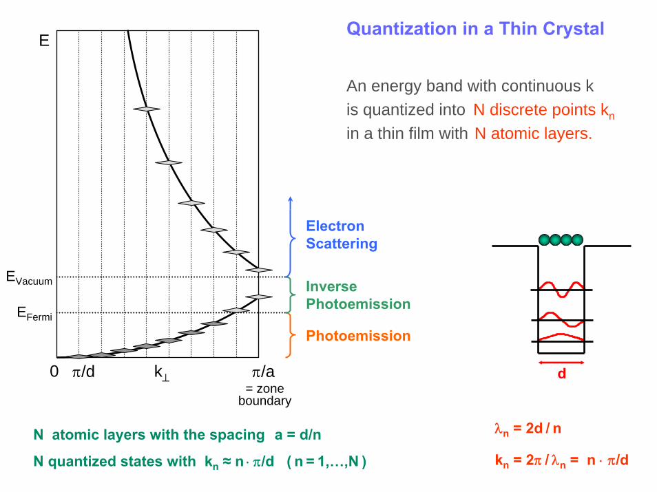
N atomic layers with the spacing a = d/n
N quantized states with kn ≈ n ⋅ π/d ( n = 1,…,N )
Quantization in a Thin Crystal
An energy band with continuous k is quantized into N discrete points kn
in a thin film with N atomic layers.
λn = 2d / n
kn = 2π / λn = n ⋅ π/d
d
E
0 π/aπ/d
EFermi
EVacuum
Photoemission
Inverse Photoemission
Electron Scattering
k⊥= zone
boundary

N atomic layers with spacing a = d/n :
⇒ N quantized states with kn ≈ N ⋅ π/d
Quantization in Thin Graphite FilmsE
0 π/aπ/d
EFermi
EVacuum
Photoemission
Lect. 7b, Slide 11
k⊥
1 layer = graphene
2 layers
3 layers
4 layers
∞ layers = graphite

Quantum Well States in Thin Films
discrete for small N
becoming continuous for N → ∞
Paggel et al.Science 283, 1709 (1999)

101616
161616
16
13
1414
11.5
13
1413
14
hν (eV)Ag/Fe(100)
Binding Energy (eV)012
Pho
toem
issi
on In
tens
ity (a
rb. u
nits
)
1
2
3
45
6
7
8
9
10
11
13
14
15
12
N
1
3
2
4
101616
161616
16
13
1414
11.5
13
1413
14
hν (eV)Ag/Fe(100)
Binding Energy (eV)012
Pho
toem
issi
on In
tens
ity (a
rb. u
nits
)
1
2
3
45
6
7
8
9
10
11
13
14
15
12
N
1
3
2
4
n
Periodic Fermi level crossing of quantum well states with
increasing thickness
Counting Quantum Well States
Number of monolayers N
Bin
ding
Ene
rgy
(eV)
0
1
2
1 2 3 4 5
6
7
8
(a) Quantum Well States for Ag/Fe(100)
n

Kawakami et al.Nature 398, 132 (1999)
HimpselScience 283, 1655 (1999)
Quantum Well Oscillations in Electron Interferometers
Fabry-Perot interferometer model: Interfaces act like mirrors for electrons. Since electrons have so short wavelengths, the interfaces need to be atomically precise.
n
12
34
56

The Important Electrons in a Metal
Energy ≈ EFermi
Energy Spread ≈ 3.5 kBT
Transport (conductivity, magnetoresistance, screening length, ...)
Width of the Fermi function:
FWHM ≈ 3.5 kBT
Phase transitions (superconductivity, magnetism, ...)
Superconducting gap:
Eg ≈ 3.5 kBTc (Tc= critical temperature)

Energy Bands of Ferromagnets
States near the Fermi level cause the energy splitting between majority and minority spin bands in a ferromagnet (red and green).
-10
-8
-6
-4
-2
0
2
4
Γ XK
Ni
Ener
gy R
elat
ive
to E
F[e
V]
0.7 0.9 1.1k|| along [011] [Å-1 ]
Calculation Photoemission data

(Qiu, et al.PR B ‘92)
Quantum Well States and Magnetic CouplingThe magnetic coupling between layers plays a key role in giant magnetoresistance(GMR), the Nobel prize winning technology used for reading heads of hard disks.
This coupling oscillates in sync with the density of states at the Fermi level.
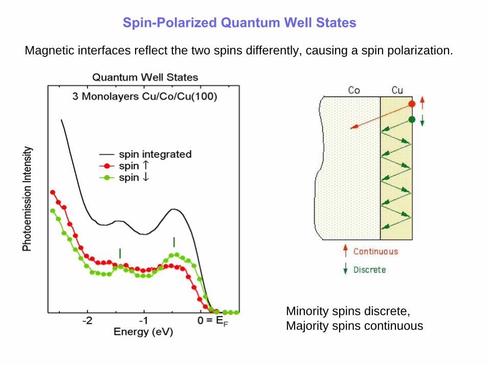
Minority spins discrete,Majority spins continuous
Magnetic interfaces reflect the two spins differently, causing a spin polarization.
Spin-Polarized Quantum Well States

Filtering mechanisms
• Interface: Spin-dependent Reflectivity ⇔ Quantum Well States
• Bulk: Spin-dependent Mean Free Path ⇔ Magnetic “Doping”
Parallel Spin Filters → Resistance Low
Opposing Spin Filters → Resistance High
Giant Magnetoresistance and Spin - Dependent Scattering

Giant Magnetoresistance (GMR):(Metal spacer, here Cu)
Tunnel Magnetoresistance (TMR):(Insulating spacer, MgO)
MagnetoelectronicsSpin currents instead of charge currents
Magnetoresistance = Change of the resistance in a magnetic field