Quad SPST CMOS Analog Switches - Maxim Integrated · PBX, PABX Guidance and Control Systems Head Up...
12
General Description The DG201A and DG211 are normally closed, quad single-pole single-throw (SPST) analog switches. These CMOS switches can be continuously operated with power supplies ranging from ±4.5V to ±18V. Maxim guarantees that these switches will not latch up if the power supplies are disconnected with input signals still connected. Both devices have guaranteed break-before-make switching. The DG201A differs from the DG211 primari- ly in switching speeds. The DG201A has a maximum turn-off time of 450ns and a maximum turn-on time of 600ns. The DG211 has a maximum turn-off time of 500ns and a maximum turn-on time of 1000ns. Compared to the original manufacturer’s products, Maxim’s DG201A and DG211 consume significantly lower power making them better suited for portable applications. Maxim has also eliminated the need for the third (V L ) power supply that is required for the oper- ation of the original manufacturer’s DG211. Applications Winchester Disk Drives Test Equipment Communications Systems PBX, PABX Guidance and Control Systems Head Up Displays Military Radios Features ♦ Guaranteed ±4.5V to ±18V Operation ♦ No V L Supply Required ♦ Nonlatching with Supplies Turned Off and Input Signals Present ♦ CMOS and TTL Logic Compatible ♦ Monolithic, Low-Power CMOS Design DG201A/DG211 Quad SPST CMOS Analog Switches ________________________________________________________________ Maxim Integrated Products 1 TOP VIEW DIP/SO/TSSOP LOGIC SWITCH 0 1 ON OFF 16 15 14 13 12 11 10 9 1 2 3 4 5 6 7 8 IN2 D2 S2 V+ V- S1 D1 IN1 DG201A DG211 N.C. S3 D3 IN3 IN4 D4 S4 GND Pin Configurations Ordering Information 19-3959; Rev 2; 5/06 For pricing, delivery, and ordering information, please contact Maxim/Dallas Direct! at 1-888-629-4642, or visit Maxim’s website at www.maxim-ic.com. PART TEMP RANGE PIN-PACKAGE DG201ACUE 0°C to +70°C 16 TSSOP DG201ACSE 0°C to +70°C 16 SO DG201ACJ 0°C to +70°C 16 Plastic DIP DG201C/D 0°C to +70°C Dice DG201AEGE -40°C to +85°C 16 QFN (5 ✕ 5) DG201AEUE -40°C to +85°C 16 TSSOP DG201ADY -40°C to +85°C 16 SO DG201ADJ -40°C to +85°C 16 Plastic DIP DG201AAK -55°C to +125°C 16 CERDIP DG201ABK -25°C to +85°C 16 CERDIP DG211CUE 0°C to +70°C 16 TSSOP DG211CSE 0°C to +70°C 16 SO DG211CJ 0°C to +70°C 16 Plastic DIP DG211C/D 0°C to +70°C Dice DG211EGE -40°C to +85°C 16 QFN (5 ✕ 5) DG211EUE -40°C to +85°C 16 TSSOP DG211DY -40°C to +85°C 16 SO DG211DJ -40°C to +85°C 16 Plastic DIP 16 15 14 13 12 11 10 9 1 2 3 4 5 6 7 8 +15V DG201A DG211 -15V VIN x 10V * * * * 5kΩ 10kΩ 40kΩ 20kΩ 5kΩ VOUT PROGRAMMABLE GAIN AMPLIFIER NOTE: *PINS 1, 8, 9, AND 16 ARE LOGIC CONTROL INPUTS Typical Operating Circuit Pin Configurations continued at end of data sheet.
Transcript of Quad SPST CMOS Analog Switches - Maxim Integrated · PBX, PABX Guidance and Control Systems Head Up...
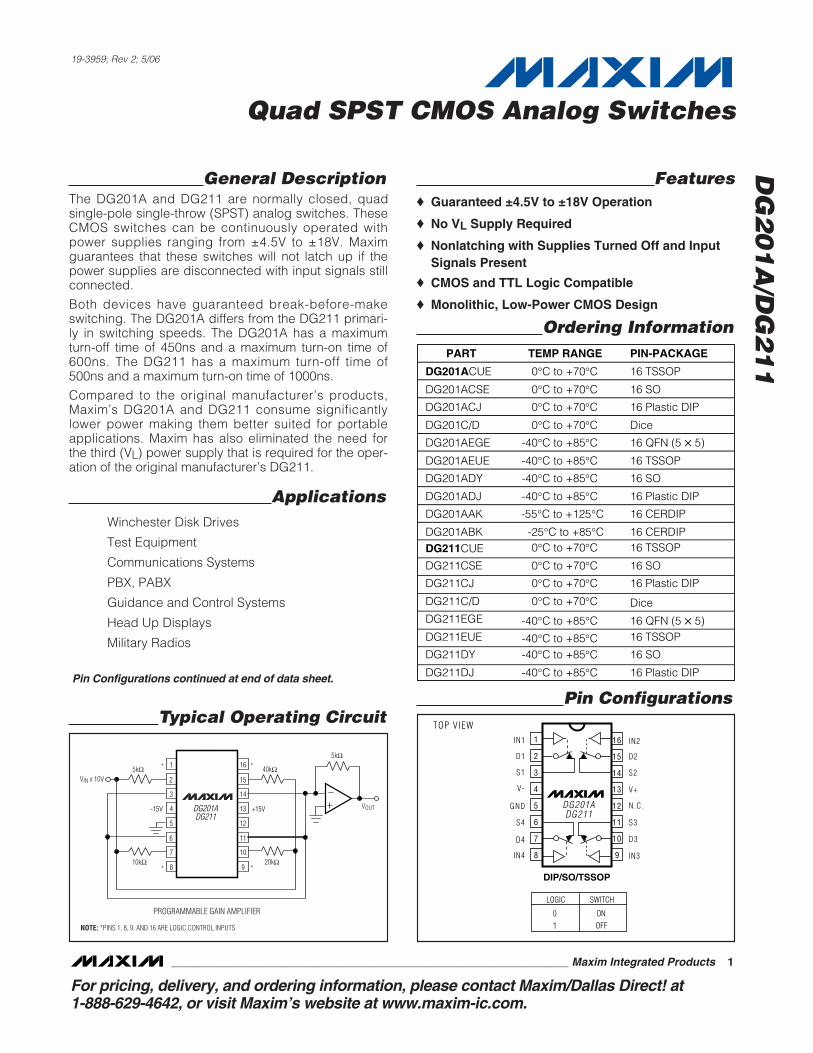
General DescriptionThe DG201A and DG211 are normally closed, quadsingle-pole single-throw (SPST) analog switches. TheseCMOS switches can be continuously operated withpower supplies ranging from ±4.5V to ±18V. Maximguarantees that these switches will not latch up if thepower supplies are disconnected with input signals stillconnected.
Both devices have guaranteed break-before-makeswitching. The DG201A differs from the DG211 primari-ly in switching speeds. The DG201A has a maximumturn-off time of 450ns and a maximum turn-on time of600ns. The DG211 has a maximum turn-off time of500ns and a maximum turn-on time of 1000ns.
Compared to the original manufacturer’s products,Maxim’s DG201A and DG211 consume significantlylower power making them better suited for portableapplications. Maxim has also eliminated the need forthe third (VL) power supply that is required for the oper-ation of the original manufacturer’s DG211.
ApplicationsWinchester Disk Drives
Test Equipment
Communications Systems
PBX, PABX
Guidance and Control Systems
Head Up Displays
Military Radios
Features♦ Guaranteed ±4.5V to ±18V Operation
♦ No VL Supply Required
♦ Nonlatching with Supplies Turned Off and InputSignals Present
♦ CMOS and TTL Logic Compatible
♦ Monolithic, Low-Power CMOS Design
DG
20
1A
/DG
21
1
Quad SPST CMOS Analog Switches
________________________________________________________________ Maxim Integrated Products 1
TOP VIEW
DIP/SO/TSSOP
LOGIC SWITCH
01
ONOFF
16
15
14
13
12
11
10
9
1
2
3
4
5
6
7
8
IN2
D2
S2
V+V-
S1
D1
IN1
DG201ADG211
N.C.
S3
D3
IN3IN4
D4
S4
GND
Pin Configurations
Ordering Information
19-3959; Rev 2; 5/06
For pricing, delivery, and ordering information, please contact Maxim/Dallas Direct! at 1-888-629-4642, or visit Maxim’s website at www.maxim-ic.com.
PART TEMP RANGE PIN-PACKAGE
DG201ACUE 0°C to +70°C 16 TSSOP
DG201ACSE 0°C to +70°C 16 SO
DG201ACJ 0°C to +70°C 16 Plastic DIP
DG201C/D 0°C to +70°C Dice
DG201AEGE -40°C to +85°C 16 QFN (5 5)
DG201AEUE -40°C to +85°C 16 TSSOP
DG201ADY -40°C to +85°C 16 SO
DG201ADJ -40°C to +85°C 16 Plastic DIP
DG201AAK -55°C to +125°C 16 CERDIP
DG201ABK -25°C to +85°C 16 CERDIPDG211CUE 0°C to +70°C 16 TSSOP
DG211CSE 0°C to +70°C 16 SO
DG211CJ 0°C to +70°C 16 Plastic DIP
DG211C/D 0°C to +70°C DiceDG211EGE -40°C to +85°C 16 QFN (5 5)DG211EUE -40°C to +85°C 16 TSSOP
DG211DY -40°C to +85°C 16 SO
DG211DJ -40°C to +85°C 16 Plastic DIP
16
15
14
13
12
11
10
9
1
2
3
4
5
6
7
8
+15VDG201ADG211
-15V
VIN x 10V
* *
* *
5kΩ
10kΩ
40kΩ
20kΩ
5kΩ
VOUT
PROGRAMMABLE GAIN AMPLIFIER
NOTE: *PINS 1, 8, 9, AND 16 ARE LOGIC CONTROL INPUTS
Typical Operating Circuit
Pin Configurations continued at end of data sheet.
DG
20
1A
/DG
21
1
Quad SPST CMOS Analog Switches
2 _______________________________________________________________________________________
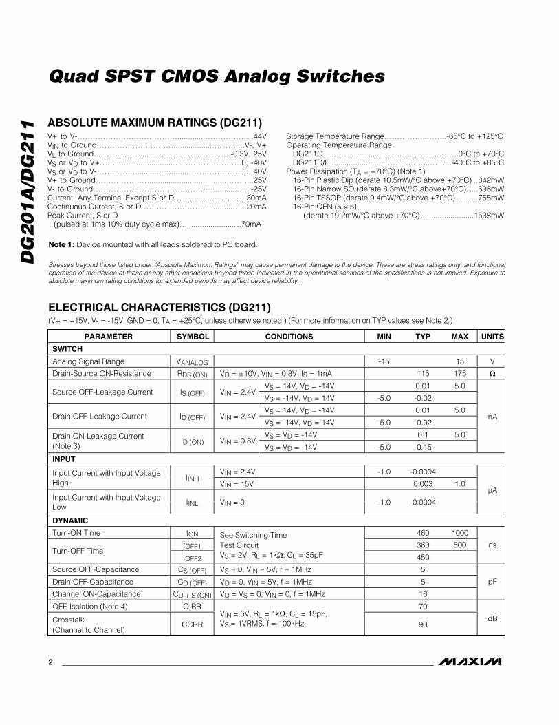
ABSOLUTE MAXIMUM RATINGS (DG211)
ELECTRICAL CHARACTERISTICS (DG211)(V+ = +15V, V- = -15V, GND = 0, TA = +25°C, unless otherwise noted.) (For more information on TYP values see Note 2.)
Stresses beyond those listed under “Absolute Maximum Ratings” may cause permanent damage to the device. These are stress ratings only, and functionaloperation of the device at these or any other conditions beyond those indicated in the operational sections of the specifications is not implied. Exposure toabsolute maximum rating conditions for extended periods may affect device reliability.
V+ to V-………………………………….............……………….44VVIN to Ground…………………………..................…. ……...V-, V+VL to Ground………....................……………………….-0.3V, 25VVS or VD to V+……...........................………………………0, -40VVS or VD to V-……………........................…………………..0, 40VV+ to Ground…………………...................................………...25VV- to Ground…………………………………….................…...-25VCurrent, Any Terminal Except S or D……….............……...30mAContinuous Current, S or D……………………..............…...20mAPeak Current, S or D
(pulsed at 1ms 10% duty cycle max)…..........................70mA
Storage Temperature Range……………..……..-65°C to +125°COperating Temperature Range
DG211C................................……………...……...0°C to +70°CDG211D/E .........................……………...……...-40°C to +85°C
Power Dissipation (TA = +70°C) (Note 1)16-Pin Plastic Dip (derate 10.5mW/°C above +70°C) ..842mW16-Pin Narrow SO (derate 8.3mW/°C above+70°C). ....696mW16-Pin TSSOP (derate 9.4mW/°C above +70°C) ..........755mW16-Pin QFN (5 5)
(derate 19.2mW/°C above +70°C).........................1538mW
PARAMETER SYMBOL CONDITIONS MIN TYP MAX UNITS
SWITCH
Analog Signal Range VANALOG -15 15 V
Drain-Source ON-Resistance RDS (ON) VD = ±10V, VIN = 0.8V, IS = 1mA 115 175 ΩVS = 14V, VD = -14V 0.01 5.0
Source OFF-Leakage Current IS (OFF) VIN = 2.4VVS = -14V, VD = 14V -5.0 -0.02
VS = 14V, VD = -14V 0.01 5.0Drain OFF-Leakage Current ID (OFF) VIN = 2.4V
VS = -14V, VD = 14V -5.0 -0.02
VS = VD = -14V 0.1 5.0Drain ON-Leakage Current(Note 3)
ID (ON) VIN = 0.8VVS = VD = -14V -5.0 -0.15
nA
INPUT
VIN = 2.4V -1.0 -0.0004Input Current with Input VoltageHigh
IINHVIN = 15V 0.003 1.0
Input Current with Input VoltageLow
IINL VIN = 0 -1.0 -0.0004
µA
DYNAMIC
Turn-ON Time tON 460 1000
tOFF1 360 500Turn-OFF Time
tOFF2
See Switching TimeTest CircuitVS = 2V, RL = 1kΩ, CL = 35pF 450
ns
Source OFF-Capacitance CS (OFF) VS = 0, VIN = 5V, f = 1MHz 5
Drain OFF-Capacitance CD (OFF) VD = 0, VIN = 5V, f = 1MHz 5
Channel ON-Capacitance CD + S (ON) VD = VS = 0, VIN = 0, f = 1MHz 16
pF
OFF-Isolation (Note 4) OIRR 70
Crosstalk(Channel to Channel)
CCRRVIN = 5V, RL = 1kΩ, CL = 15pF,VS = 1VRMS, f = 100kHz 90
dB
Note 1: Device mounted with all leads soldered to PC board.
DG
20
1A
/DG
21
1
Quad SPST CMOS Analog Switches
_______________________________________________________________________________________ 3
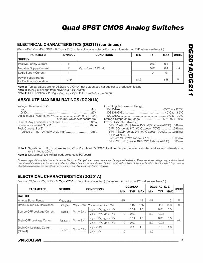
ABSOLUTE MAXIMUM RATINGS (DG201A)
Voltages Reference to V-V+………………………………………………..……………..44VGND……………………………………………..……….…….25V
Digital Inputs (Note 1), VS, VD............................-2V to (V+ + 2V) or 20mA, whichever occurs first
Current, Any Terminal Except S or D………..….…………...30mAContinuous Current, S or D…………………………………...20mAPeak Current, S or D
(pulsed at 1ms 10% duty cycle max)…………………….70mA
Operating Temperature RangeDG201AA.............…………........………..…...-55°C to +125°CDG201AD/E .........………………….....…..….…-40°C to +85°C DG201AC .............………........................…….…0°C to +70°C
Storage Temperature Range………………..…..-65°C to +150°CPower Dissipation (Note 2)
16-Pin Plastic Dip (derate 10.5mW/°C above +70°C) ...842mW16-Pin SO (derate 8.7mW/°C above +70°C) .................696mW16-Pin TSSOP (derate 9.4mW/°C above +70°C) ...........755mW16-Pin QFN (5 5)
(derate 19.2mW/°C above +70°C)...........................1538mW16-Pin CERDIP (derate 10.0mW/°C above +70°C)......800mW
Stresses beyond those listed under “Absolute Maximum Ratings” may cause permanent damage to the device. These are stress ratings only, and functionaloperation of the device at these or any other conditions beyond those indicated in the operational sections of the specifications is not implied. Exposure toabsolute maximum rating conditions for extended periods may affect device reliability.
DG201AA DG201AC, D, EPARAMETER SYMBOL CONDITIONS
MIN TYP MAX MIN TYP MAXUNITS
SWITCH
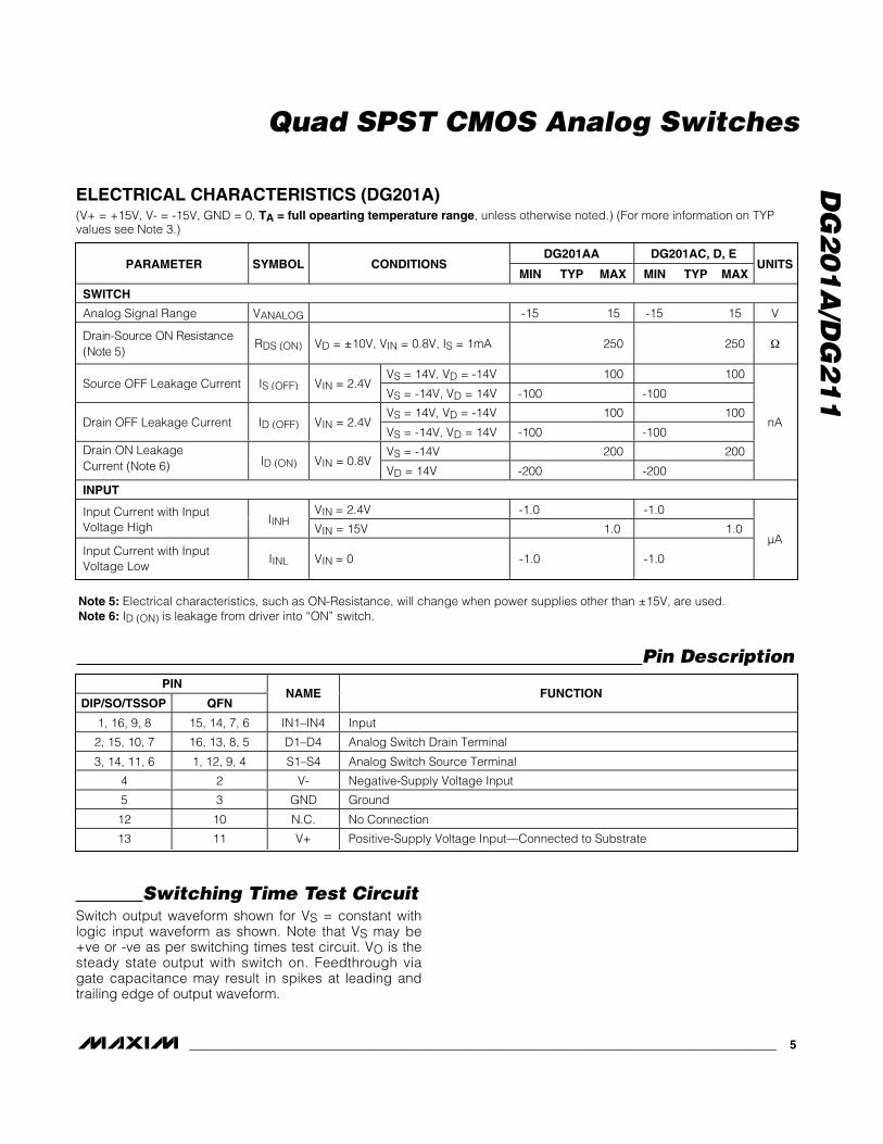
Analog Signal Range VANALOG -15 15 -15 15 V
Drain-Source ON Resistance RDS (ON) VD = ±10V, VIN = 0.8V, IS = 1mA 115 175 115 200 Ω
VS = 14V, VD = -14V 0.01 1.0 0.01 5.0Source OFF-Leakage Current IS (OFF) VIN = 2.4V
VS = -14V, VD = 14V -1.0 -0.02 -5.0 -0.02
VS = 14V, VD = -14V 0.01 1.0 0.01 5.0Drain OFF-Leakage Current ID (OFF) VIN = 2.4V
VS = -14V, VD = 14V -1.0 -0.02 -5.0 -0.02
VS = -14V 0.1 1.0 0.1 1.0Drain ON-Leakage Current(Note 4)
ID (ON) VIN = 0.8VVS = 14V -1.0 -1.0
nA
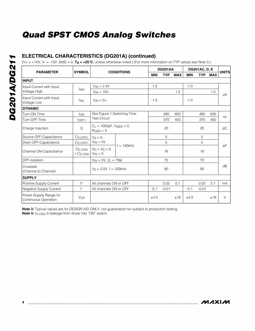
ELECTRICAL CHARACTERISTICS (DG201A)(V+ = +15V, V- = -15V, GND = 0, TA = +25°C, unless otherwise noted.) (For more information on TYP values see Note 3.)
ELECTRICAL CHARACTERISTICS (DG211) (continued)(V+ = +15V, V- = -15V, GND = 0, TA = +25°C, unless otherwise noted.) (For more information on TYP values see Note 2.)
PARAMETER SYMBOL CONDITIONS MIN TYP MAX UNITS
SUPPLY
Positive Supply Current I+ 0.02 0.4
Negative Supply Current I- 0.01 0.4
Logic Supply Current IL
VIN = 0 and 2.4V (all)
0 0
mA
Power-Supply Rangefor Continous Operation
VOP ±4.5 ±18 V
Note 1: Signals on S_, D_, or IN_ exceeding V+ or V- on Maxim’s DG201A will be clamped by internal diodes, and are also internally cur-rent limited to 25mA.
Note 2: Device mounted with all leads soldered to PC board.
Note 2: Typical values are for DESIGN AID ONLY, not guaranteed nor subject to production testing.Note 3: ID(ON) is leakage from driver into “ON” switch.Note 4: OFF-Isolation = 20 log VS/VD, VS = input to OFF switch, VD = output.
DG
20
1A
/DG
21
1
Quad SPST CMOS Analog Switches
4 _______________________________________________________________________________________
Note 3: Typical values are for DESIGN AID ONLY, not guaranteed nor subject to production testing.Note 4: ID (ON) is leakage from driver into “ON” switch.
DG201AA DG201AC, D, EPARAMETER SYMBOL CONDITIONS
MIN TYP MAX MIN TYP MAXUNITS
INPUT
VIN = 2.4V -1.0 -1.0Input Current with InputVoltage High
IINHVIN = 15V 1.0 1.0
Input Current with InputVoltage Low
IINL VIN = 0+ -1.0 -1.0
µA
DYNAMIC
Turn-ON Time tON 480 600 480 600
Turn-OFF Time tOFF1
See Figure 1 Switching TimeTest Circuit 370 450 370 450
ns
Charge Injection QCL = 1000pF, VGEN = 0,RGEN = 0
20 20 pC
Source OFF-Capacitance CS (OFF) 5 5
Drain OFF-Capacitance CD (OFF)
VS = 0,VIN = 5V 5 5
Channel ON-CapacitanceCD (ON)
+ CS (ON)
VD = VS = 0,VIN = 0
f = 140kHz
16 16
pF
OFF-Isolation VIN = 5V, ZL = 75Ω 70 70
Crosstalk(Channel to Channel)
VS = 2.0V, f = 100kHz 90 90dB
SUPPLY
Positive Supply Current I+ All channels ON or OFF 0.02 0.1 0.02 0.1 mA
Negative Supply Current I- All channels ON or OFF -0.1 -0.01 -0.1 -0.01
Power-Supply Range forContinuous Operation
VOP ±4.5 ±18 ±4.5 ±18 V
ELECTRICAL CHARACTERISTICS (DG201A) (continued)(V+ = +15V, V- = -15V, GND = 0, TA = +25°C, unless otherwise noted.) (For more information on TYP values see Note 3.)
_______________________________________________________________________________________ 5
DG
20
1A
/DG
21
1
Quad SPST CMOS Analog Switches
ELECTRICAL CHARACTERISTICS (DG201A)(V+ = +15V, V- = -15V, GND = 0, TA = full opearting temperature range, unless otherwise noted.) (For more information on TYP values see Note 3.)
DG201AA DG201AC, D, EPARAMETER SYMBOL CONDITIONS
MIN TYP MAX MIN TYP MAXUNITS
SWITCH
Analog Signal Range VANALOG -15 15 -15 15 V
D r ai n- S our ce ON Resi stance( N ote 5)
RDS (ON) VD = ±10V, VIN = 0.8V, IS = 1mA 250 250 Ω
VS = 14V, VD = -14V 100 100Source OFF Leakage Current IS (OFF) VIN = 2.4V
VS = -14V, VD = 14V -100 -100
VS = 14V, VD = -14V 100 100Drain OFF Leakage Current ID (OFF) VIN = 2.4V
VS = -14V, VD = 14V -100 -100
VS = -14V 200 200Drain ON LeakageCurrent (Note 6) ID (ON) VIN = 0.8V
VD = 14V -200 -200
nA
INPUT
VIN = 2.4V -1.0 -1.0Input Current with InputVoltage High
IINHVIN = 15V 1.0 1.0
Input Current with InputVoltage Low
IINL VIN = 0 -1.0 -1.0
µA
Note 5: Electrical characteristics, such as ON-Resistance, will change when power supplies other than ±15V, are used.Note 6: ID (ON) is leakage from driver into “ON” switch.
PIN
DIP/SO/TSSOP QFNNAME FUNCTION
1, 16, 9, 8 15, 14, 7, 6 IN1–IN4 Input
2, 15, 10, 7 16, 13, 8, 5 D1–D4 Analog Switch Drain Terminal
3, 14, 11, 6 1, 12, 9, 4 S1–S4 Analog Switch Source Terminal
4 2 V- Negative-Supply Voltage Input
5 3 GND Ground
12 10 N.C. No Connection
13 11 V+ Positive-Supply Voltage Input—Connected to Substrate
Pin Description
Switching Time Test CircuitSwitch output waveform shown for VS = constant withlogic input waveform as shown. Note that VS may be+ve or -ve as per switching times test circuit. VO is thesteady state output with switch on. Feedthrough viagate capacitance may result in spikes at leading andtrailing edge of output waveform.
DG
20
1A
/DG
21
1
Quad SPST CMOS Analog Switches
6 _______________________________________________________________________________________
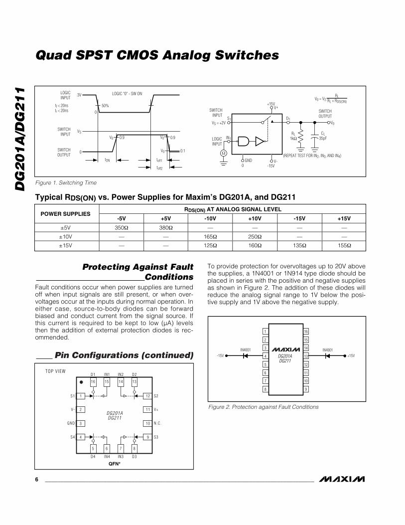
RDS(ON) AT ANALOG SIGNAL LEVELPOWER SUPPLIES
-5V +5V -10V +10V -15V +15V
±5V 350Ω 380Ω — — — —
±10V — — 165Ω 250Ω — —
±15V — — 125Ω 160Ω 135Ω 155Ω
Typical RDS(ON) vs. Power Supplies for Maxim’s DG201A, and DG211
Protecting Against Fault Conditions
Fault conditions occur when power supplies are turnedoff when input signals are still present, or when over-voltages occur at the inputs during normal operation. Ineither case, source-to-body diodes can be forwardbiased and conduct current from the signal source. Ifthis current is required to be kept to low (µA) levelsthen the addition of external protection diodes is rec-ommended.
To provide protection for overvoltages up to 20V abovethe supplies, a 1N4001 or 1N914 type diode should beplaced in series with the positive and negative suppliesas shown in Figure 2. The addition of these diodes willreduce the analog signal range to 1V below the posi-tive supply and 1V above the negative supply.
16
15
14
13
12
11
10
9
1
2
3
4
5
6
7
8
DG201ADG211
IN4001-15V
IN4001+15V
Figure 2. Protection against Fault Conditions
LOGIC "0" - SW ON3V
VS
0
LOGICINPUT
tf < 20nstr < 20ns
SWITCHINPUT
SWITCHOUTPUT
50%0
V0 0.9
tON
V0
V0
0.9
0.1
toff1
toff2
Ω
SWITCHINPUT
S1VS = +2V
IN1LOGICINPUT
GND0
V--15V
+15VV+
D1
RL1kΩ
CL35pF
V0
SWITCHOUTPUT
(REPEAT TEST FOR IN2, IN3, AND IN4)
V0 = VSRL
RL + RDS(ON)
TOP VIEW
16 15 14 13
5
1
2
3
4
12
11
10
9
6 7 8
S1
V-
GND
S4
S2
V+
N.C.
S3
D1 IN1 IN2 D2
D4 IN4 IN3 D3
DG201ADG211
QFN*
Pin Configurations (continued)
Figure 1. Switching Time
DG
20
1A
/DG
21
1
Quad SPST CMOS Analog Switches
_______________________________________________________________________________________ 7
SO
ICN
.EP
S
PACKAGE OUTLINE, .150" SOIC
11
21-0041 BREV.DOCUMENT CONTROL NO.APPROVAL
PROPRIETARY INFORMATION
TITLE:
TOP VIEW
FRONT VIEW
MAX
0.010
0.069
0.019
0.157
0.010
INCHES
0.150
0.007
E
C
DIM
0.014
0.004
B
A1
MIN
0.053A
0.19
3.80 4.00
0.25
MILLIMETERS
0.10
0.35
1.35
MIN
0.49
0.25
MAX
1.75
0.0500.016L 0.40 1.27
0.3940.386D
D
MINDIM
D
INCHES
MAX
9.80 10.00
MILLIMETERS
MIN MAX
16 AC
0.337 0.344 AB8.758.55 14
0.189 0.197 AA5.004.80 8
N MS012
N
SIDE VIEW
H 0.2440.228 5.80 6.20
e 0.050 BSC 1.27 BSC
C
HE
e B A1
A
D
0∞-8∞L
1
VARIATIONS:
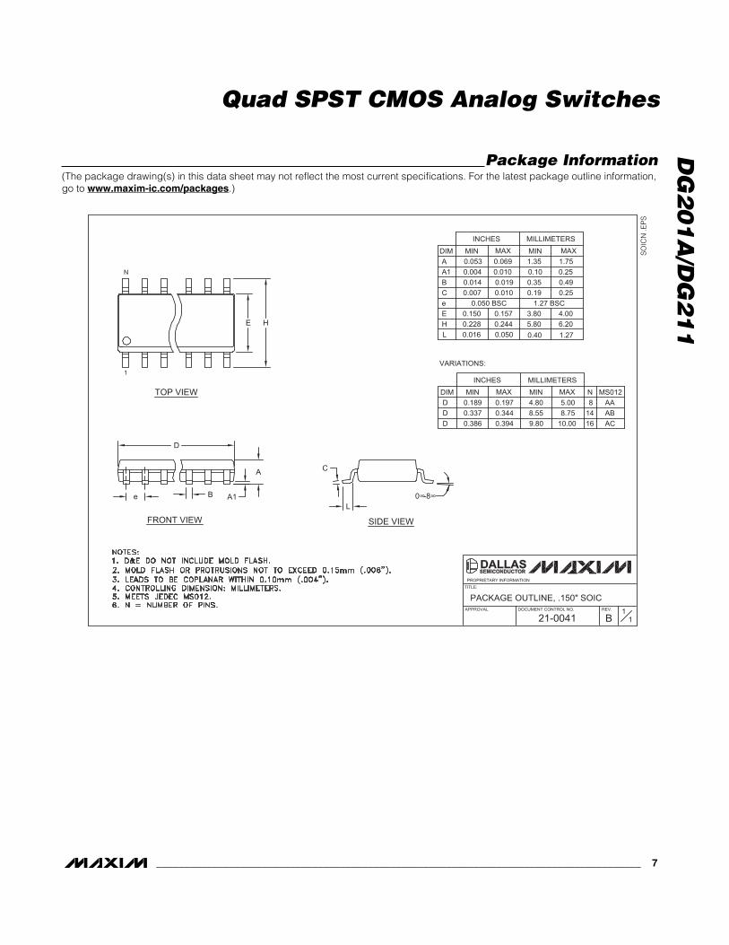
Package Information(The package drawing(s) in this data sheet may not reflect the most current specifications. For the latest package outline information,go to www.maxim-ic.com/packages.)

DG
20
1A
/DG
21
1
Quad SPST CMOS Analog Switches
8 _______________________________________________________________________________________
PD
IPN
.EP
S
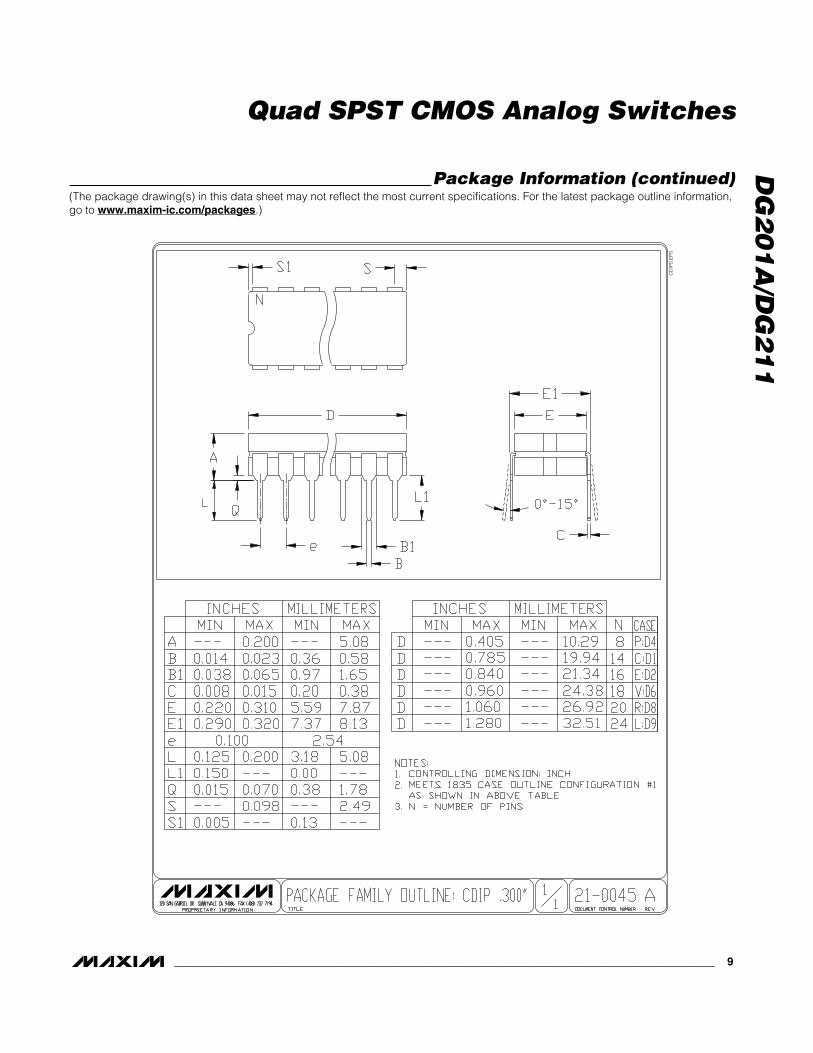
Package Information (continued)(The package drawing(s) in this data sheet may not reflect the most current specifications. For the latest package outline information,go to www.maxim-ic.com/packages.)
DG
20
1A
/DG
21
1
Quad SPST CMOS Analog Switches
_______________________________________________________________________________________ 9
CD
IPS
.EP
S
Package Information (continued)(The package drawing(s) in this data sheet may not reflect the most current specifications. For the latest package outline information,go to www.maxim-ic.com/packages.)
DG
20
1A
/DG
21
1
Quad SPST CMOS Analog Switches
10 ______________________________________________________________________________________
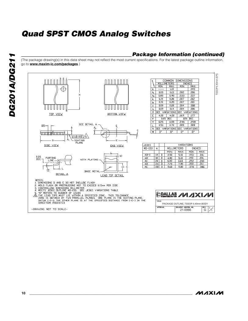
TSS
OP
4.40
mm
.EP
S
PACKAGE OUTLINE, TSSOP 4.40mm BODY
21-0066 11
G
Package Information (continued)(The package drawing(s) in this data sheet may not reflect the most current specifications. For the latest package outline information,go to www.maxim-ic.com/packages.)
DG
20
1A
/DG
21
1
Quad SPST CMOS Analog Switches
______________________________________________________________________________________ 11
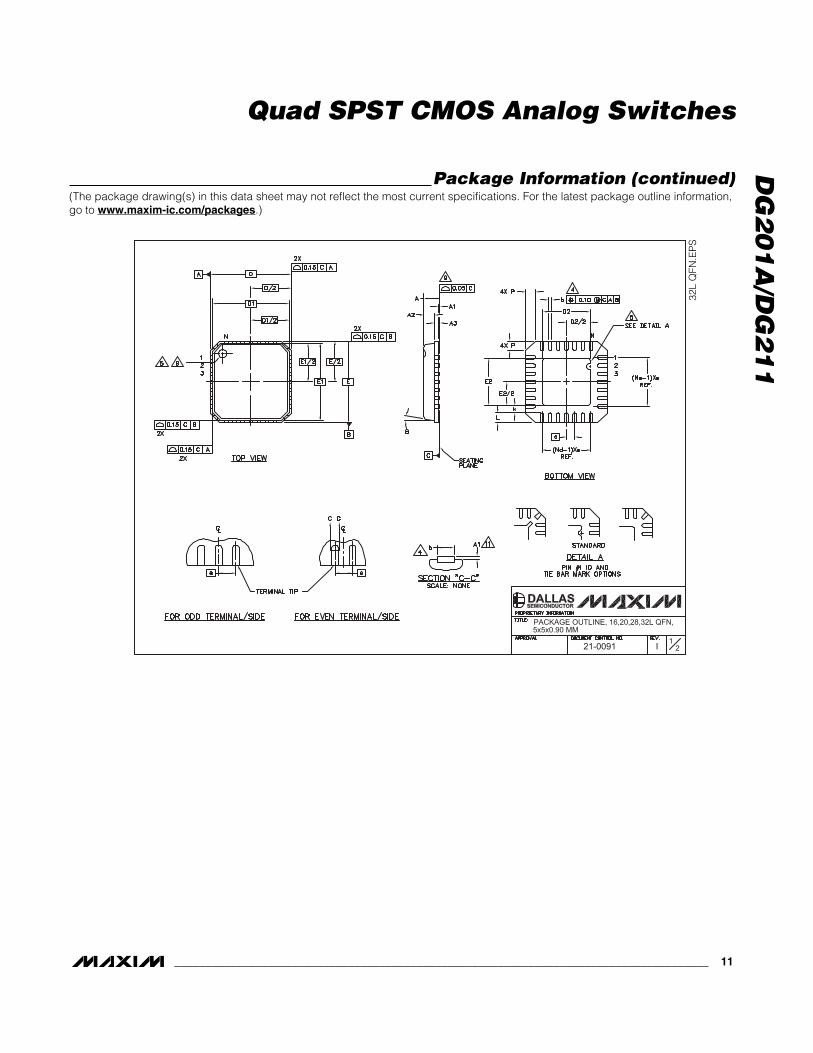
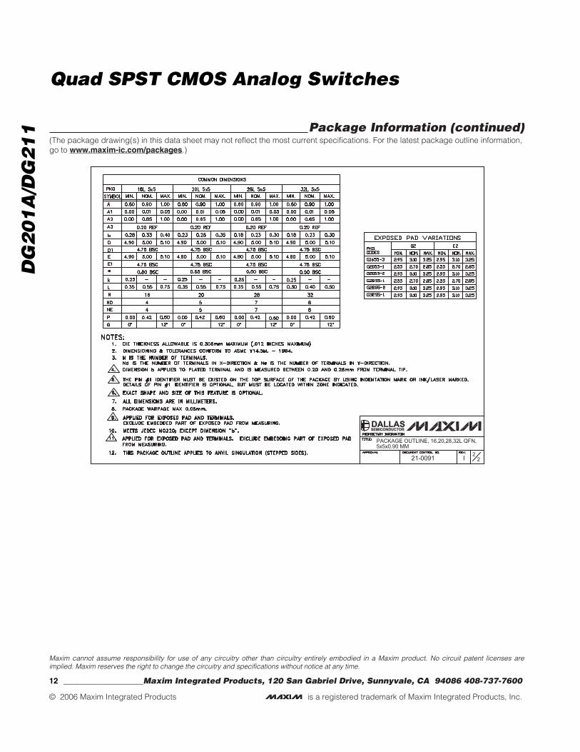
32L
QFN
.EP
S
Package Information (continued)(The package drawing(s) in this data sheet may not reflect the most current specifications. For the latest package outline information,go to www.maxim-ic.com/packages.)
DG
20
1A
/DG
21
1
Quad SPST CMOS Analog Switches
Maxim cannot assume responsibility for use of any circuitry other than circuitry entirely embodied in a Maxim product. No circuit patent licenses areimplied. Maxim reserves the right to change the circuitry and specifications without notice at any time.
12 ____________________Maxim Integrated Products, 120 San Gabriel Drive, Sunnyvale, CA 94086 408-737-7600
© 2006 Maxim Integrated Products is a registered trademark of Maxim Integrated Products, Inc.
Package Information (continued)(The package drawing(s) in this data sheet may not reflect the most current specifications. For the latest package outline information,go to www.maxim-ic.com/packages.)