Q1 Q2 Q3 Q4 Q5ese570/spring2018/handouts/final.pdf · PLH = time for output voltage to rise from V...
14
ESE570 Spring 2018 University of Pennsylvania Department of Electrical and System Engineering Digital Integrated Cicruits AND VLSI Fundamentals ESE570, Spring 2018 Final Monday, Apr 30 • 5 Problems with point weightings shown. All 5 problems must be completed. • Calculators allowed. • Closed book = No text or notes allowed. • Clearly label all final answers. Name: Grade: Q1 Q2 Q3 Q4 Q5 Total 1
Transcript of Q1 Q2 Q3 Q4 Q5ese570/spring2018/handouts/final.pdf · PLH = time for output voltage to rise from V...

ESE570 Spring 2018
University of PennsylvaniaDepartment of Electrical and System Engineering
Digital Integrated Cicruits AND VLSI Fundamentals
ESE570, Spring 2018 Final Monday, Apr 30
• 5 Problems with point weightings shown. All 5 problems must be completed.
• Calculators allowed.
• Closed book = No text or notes allowed.
• Clearly label all final answers.
Name:
Grade:
Q1
Q2
Q3
Q4
Q5
Total
1
ESE570 Spring 2018
University of PennsylvaniaDepartment of Electrical and System Engineering
Digital Integrated Cicruits AND VLSI Fundamentals
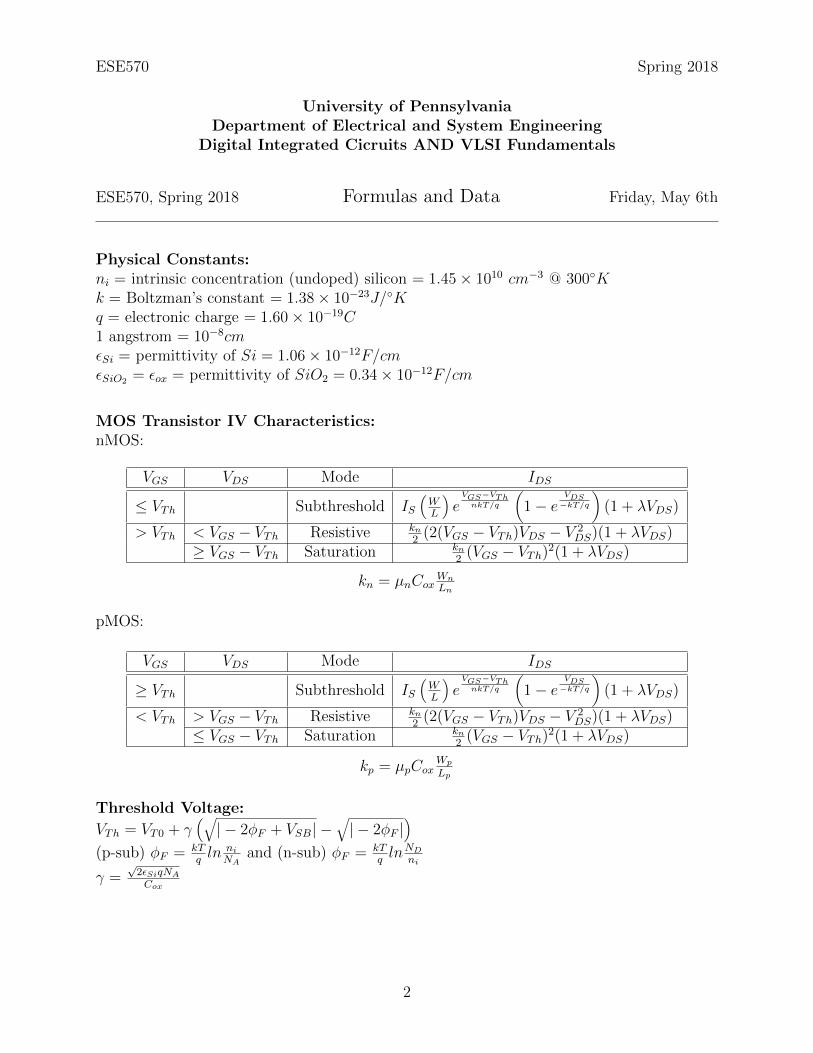
ESE570, Spring 2018 Formulas and Data Friday, May 6th
Physical Constants:ni = intrinsic concentration (undoped) silicon = 1.45× 1010 cm−3 @ 300◦Kk = Boltzman’s constant = 1.38× 10⁻²³J/◦Kq = electronic charge = 1.60× 10⁻¹⁹C1 angstrom = 10−8cmεSi = permittivity of Si = 1.06× 10⁻¹²F/cmεSiO2 = εox = permittivity of SiO2 = 0.34× 10⁻¹²F/cm
MOS Transistor IV Characteristics:nMOS:
VGS VDS Mode IDS
≤ VTh Subthreshold IS(WL
)e
VGS−VThnkT/q
(1− e
VDS−kT/q
)(1 + λVDS)
> VTh < VGS − VTh Resistive kn2
(2(VGS − VTh)VDS − V 2DS)(1 + λVDS)
≥ VGS − VTh Saturation kn2
(VGS − VTh)2(1 + λVDS)
kn = µnCoxWn
Ln
pMOS:
VGS VDS Mode IDS
≥ VTh Subthreshold IS(WL
)e
VGS−VThnkT/q
(1− e
VDS−kT/q
)(1 + λVDS)
< VTh > VGS − VTh Resistive kn2
(2(VGS − VTh)VDS − V 2DS)(1 + λVDS)
≤ VGS − VTh Saturation kn2
(VGS − VTh)2(1 + λVDS)
kp = µpCoxWp
Lp
Threshold Voltage:
VTh = VT0 + γ(√| − 2φF + VSB| −
√| − 2φF |
)(p-sub) φF = kT
qln ni
NAand (n-sub) φF = kT
qlnND
ni
γ =√
2εSiqNA
Cox
2
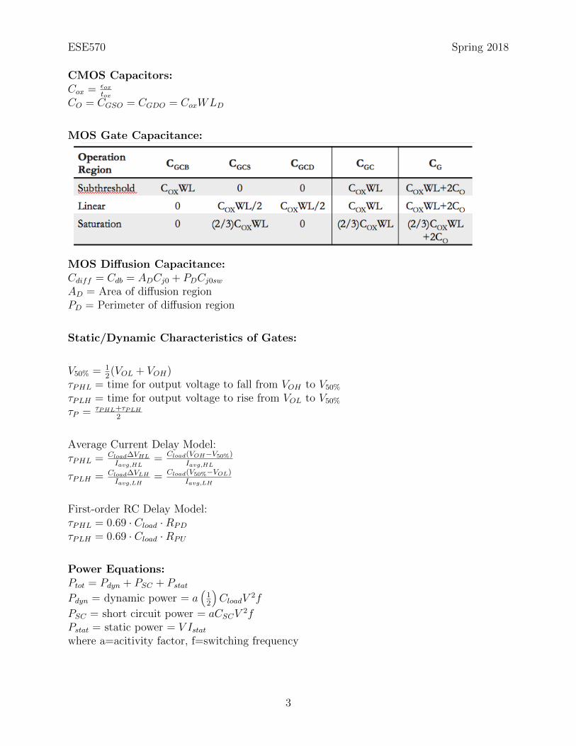
ESE570 Spring 2018
CMOS Capacitors:Cox = εox
toxCO = CGSO = CGDO = CoxWLD
MOS Gate Capacitance:
MOS Diffusion Capacitance:Cdiff = Cdb = ADCj0 + PDCj0swAD = Area of diffusion regionPD = Perimeter of diffusion region
Static/Dynamic Characteristics of Gates:
V50% = 12(VOL + VOH)
τPHL = time for output voltage to fall from VOH to V50%
τPLH = time for output voltage to rise from VOL to V50%
τP = τPHL+τPLH
2
Average Current Delay Model:τPHL = Cload∆VHL
Iavg,HL= Cload(VOH−V50%)
Iavg,HL
τPLH = Cload∆VLH
Iavg,LH= Cload(V50%−VOL)
Iavg,LH
First-order RC Delay Model:τPHL = 0.69 · Cload ·RPD
τPLH = 0.69 · Cload ·RPU
Power Equations:Ptot = Pdyn + PSC + PstatPdyn = dynamic power = a
(12
)CloadV
2f
PSC = short circuit power = aCSCV2f
Pstat = static power = V Istatwhere a=acitivity factor, f=switching frequency
3
ESE570 Spring 2018
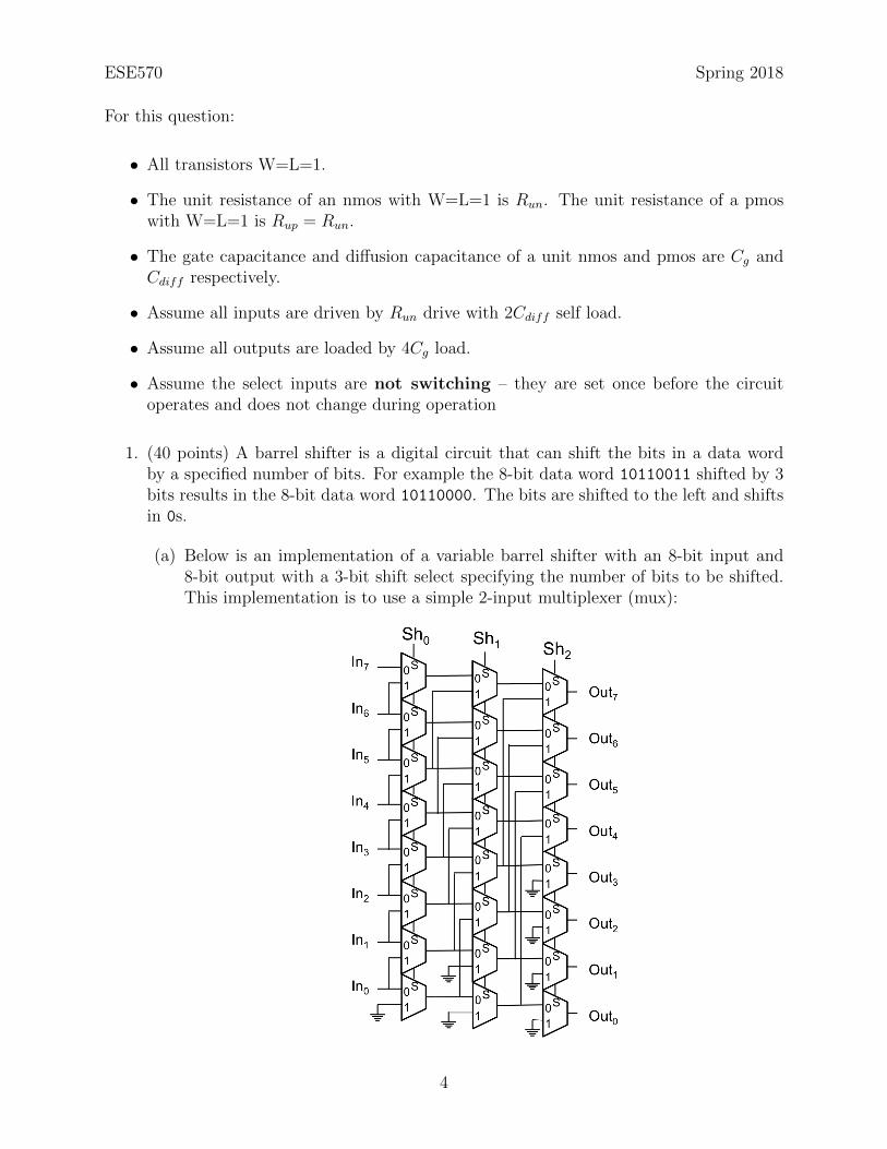
For this question:
• All transistors W=L=1.
• The unit resistance of an nmos with W=L=1 is Run. The unit resistance of a pmoswith W=L=1 is Rup = Run.
• The gate capacitance and diffusion capacitance of a unit nmos and pmos are Cg andCdiff respectively.
• Assume all inputs are driven by Run drive with 2Cdiff self load.
• Assume all outputs are loaded by 4Cg load.
• Assume the select inputs are not switching – they are set once before the circuitoperates and does not change during operation
1. (40 points) A barrel shifter is a digital circuit that can shift the bits in a data wordby a specified number of bits. For example the 8-bit data word 10110011 shifted by 3bits results in the 8-bit data word 10110000. The bits are shifted to the left and shiftsin 0s.
(a) Below is an implementation of a variable barrel shifter with an 8-bit input and8-bit output with a 3-bit shift select specifying the number of bits to be shifted.This implementation is to use a simple 2-input multiplexer (mux):
4
ESE570 Spring 2018
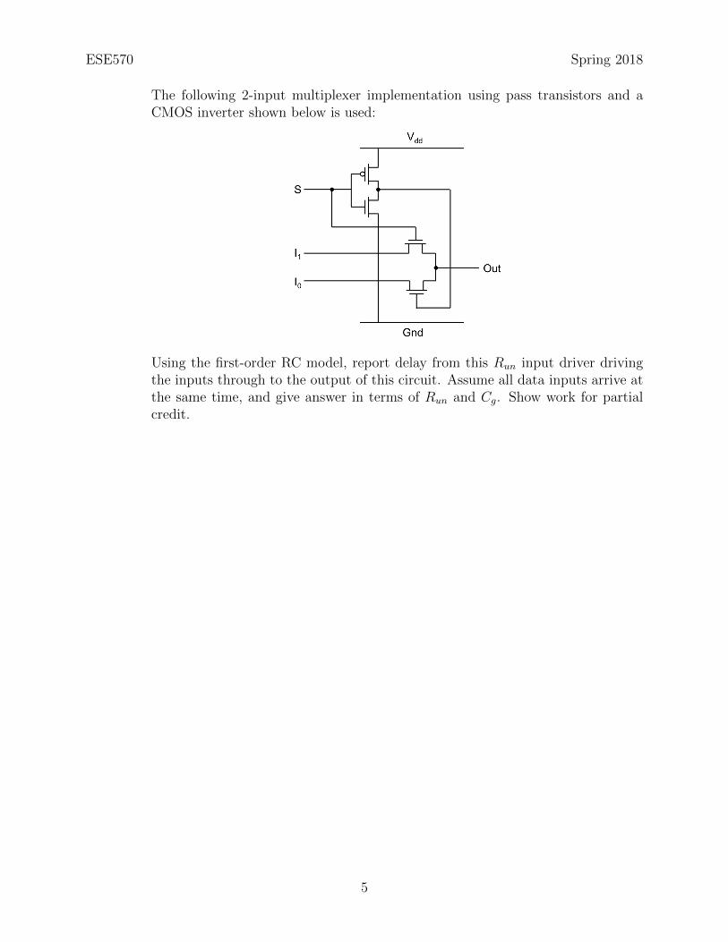
The following 2-input multiplexer implementation using pass transistors and aCMOS inverter shown below is used:
Using the first-order RC model, report delay from this Run input driver drivingthe inputs through to the output of this circuit. Assume all data inputs arrive atthe same time, and give answer in terms of Run and Cg. Show work for partialcredit.
5
ESE570 Spring 2018
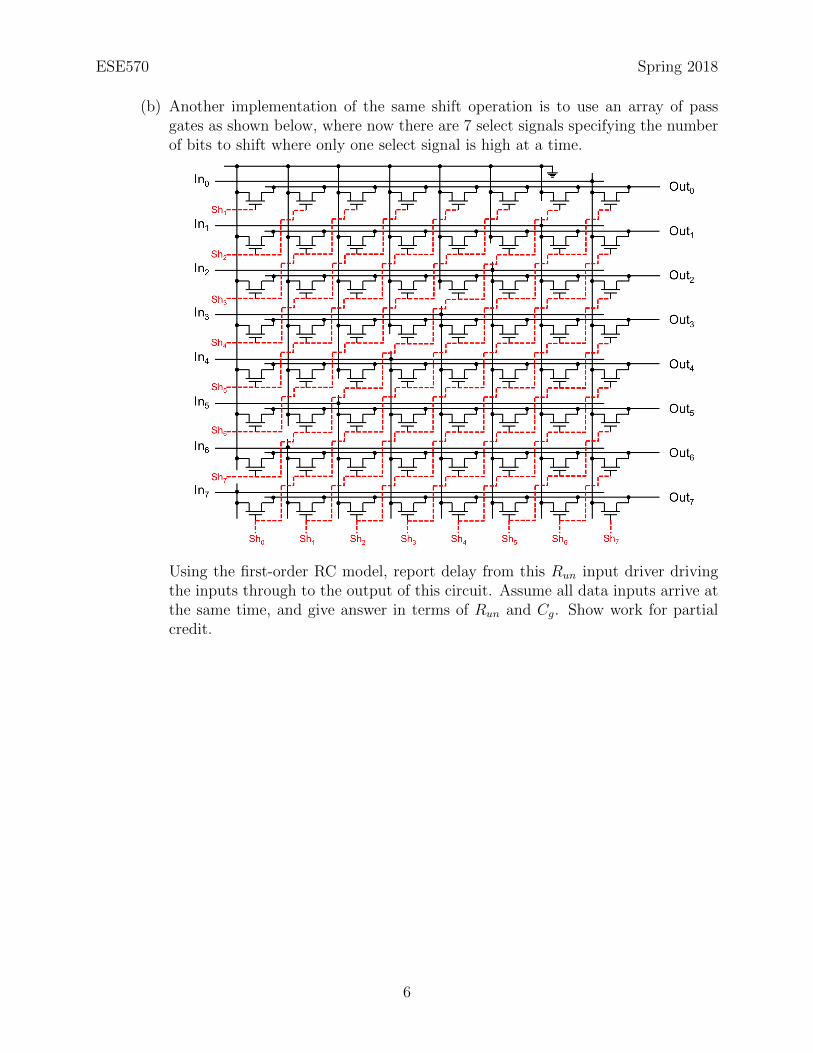
(b) Another implementation of the same shift operation is to use an array of passgates as shown below, where now there are 7 select signals specifying the numberof bits to shift where only one select signal is high at a time.
Using the first-order RC model, report delay from this Run input driver drivingthe inputs through to the output of this circuit. Assume all data inputs arrive atthe same time, and give answer in terms of Run and Cg. Show work for partialcredit.
6

ESE570 Spring 2018
(c) Compare and comment on the difference in the delay of the two implementa-tions. What is the difference between the designs that contributes to the fasterimplementation being faster?
(d) What additional circuit do you need to add to the implementation in (b) for faircomparison of designs such that the inputs and outputs are the same?
7
ESE570 Spring 2018
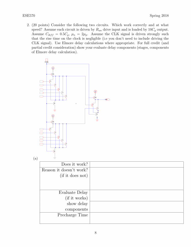
2. (20 points) Consider the following two circuits. Which work correctly and at whatspeed? Assume each circuit is driven by Run drive input and is loaded by 10Cg output.Assume Cdiff = 0.5Cg, µn = 2µp. Assume the CLK signal is driven strongly suchthat the rise time on the clock is negligible (i.e you don’t need to include driving theCLK signal). Use Elmore delay calculations where appropriate. For full credit (andpartial credit consideration) show your evaluate delay components (stages, componentsof Elmore delay calculation).
(a)
out
CLK
3
3
3
3
3
3
3
6
6
3
3
3
3
3
6
10
10
10
Does it work?
Reason it doesn’t work?(if it does not)
Evaluate Delay(if it works)show delay
components
Precharge Time
8
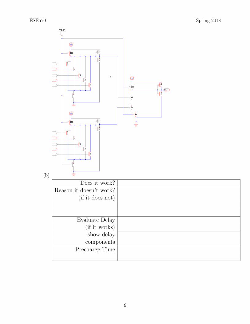
ESE570 Spring 2018
(b)
CLK
out
3
3
6
3
3
2
3
3
3
6
3
3
2
3
6
6
2
6
104
104
10
4
Does it work?
Reason it doesn’t work?(if it does not)
Evaluate Delay(if it works)show delay
components
Precharge Time
9

ESE570 Spring 2018
3. (10 points) An embedded hardware accelerator in a system-on-chip is designed in a90 nm process with a Vdd of 1 V. The circuit has 1 million logic transistors with anaverage width of 12λ. The transistor gate capacitance is Cg = 2fF/µm and the gateshave an activity factor of 0.2.
(a) What is the maximum clock frequency if the dynamic power should not exceed20 mW?
(b) If the subthreshold leakage is 20nA/µm and half the transistors are off (on aver-age), what is the leakage power?
10
ESE570 Spring 2018
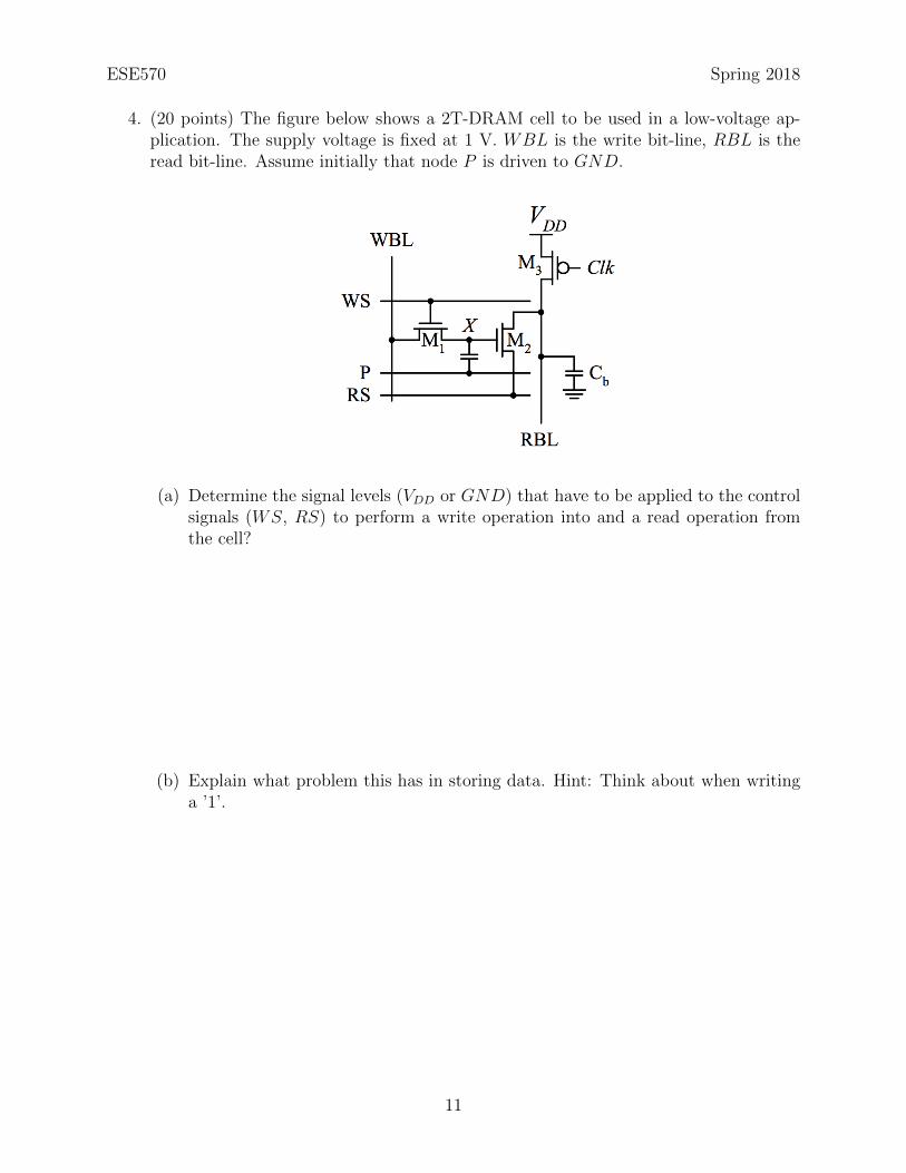
4. (20 points) The figure below shows a 2T-DRAM cell to be used in a low-voltage ap-plication. The supply voltage is fixed at 1 V. WBL is the write bit-line, RBL is theread bit-line. Assume initially that node P is driven to GND.
(a) Determine the signal levels (VDD or GND) that have to be applied to the controlsignals (WS, RS) to perform a write operation into and a read operation fromthe cell?
(b) Explain what problem this has in storing data. Hint: Think about when writinga ’1’.
11
ESE570 Spring 2018
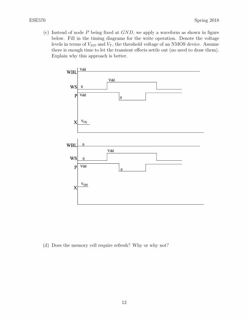
(c) Instead of node P being fixed at GND, we apply a waveform as shown in figurebelow. Fill in the timing diagrams for the write operation. Denote the voltagelevels in terms of VDD and VT , the threshold voltage of an NMOS device. Assumethere is enough time to let the transient effects settle out (no need to draw them).Explain why this approach is better.
(d) Does the memory cell require refresh? Why or why not?
12

ESE570 Spring 2018
5. (20 pts) Short Answer Questions: Answer the questions briefly. Include diagrams andequations as needed. Be clear in your explanation and handwriting.
A Draw the IV relationships between drain current and the drain-to-source voltageand gate-to-source voltage (Id vs. VGS and Id vs. VDS) Label all relevant features.
B What is velocity saturation and under what conditions does it occur in a MOSFETdevice?
C How does reducing the threshold voltage of a device impact delay and energy?
13

ESE570 Spring 2018
D How can you test if your design will meet your speed spec with variations in designparameters?
E Describe two undesired effects cause from having long wires in your design.
14