PWM-dimmable single channel LED driver with … · This is information on a product in full...
26
This is information on a product in full production. June 2014 DocID025575 Rev 3 1/26 LED6001 PWM-dimmable single channel LED driver with integrated boost controller Datasheet - production data Features Switching controller section – 5.5 V to 36 V input voltage range – Very low shutdown current: I SHDN < 10 μA – Internal +5 V LDO for gate driver supply – Internal +3.3 V LDO for device supply – Fixed frequency peak current mode control – Adjustable (100 kHz to 1 MHz) switching frequency – External synchronization for multi-device applications – High performance external MOSFET driver – Cycle-by-cycle external MOSFET OCP – Fixed internal soft-start – Programmable output OVP – Boost, buck-boost and SEPIC topologies supported – Thermal shutdown with autorestart – Output short-circuit detection LED control section – Up to 60 V output voltage – Constant current control loop – High-side output current sensing circuitry – 30 to 300 mV differential sensing voltage – ± 4% output current reference accuracy – Output overcurrent protection – Sensing resistor failure protection – PWM dimming with auxiliary series switch – Analog dimming Applications Indoor and architectural LED lighting Emergency LED lighting Off-grid LED street lighting White goods Gaming/gambling machines Description The LED6001 device is a LED driver that combines a boost controller and a high-side current sensing circuitry optimized for driving one string of high-brightness LEDs. The device is compatible with multiple topologies such as boost, SEPIC and floating load buck-boost. The brightness of the LEDs can be controlled through PWM dimming and analog dimming (10:1 ratio) by means of two independent pins. Enhanced PWM dimming can be obtained thanks to a MOSFET in series with the LED string and directly driven by a dedicated pin. The high-side current sensing, in combination with a P-channel MOSFET, provides an effective protection in case the positive terminal of the LED string is shorted to ground. The high precision current sensing circuitry allows a LED current regulation reference within 4% accuracy over the whole temperature range and production spread. A fault output (open-drain) informs the host system about faulty conditions: device overtemperature, output overvoltage (disconnected LED string) and LED overcurrent. HTSSOP-16 Table 1. Device summary Order code Package Packaging LED6001 HTSSOP-16 (exposed pad) Tube LED6001TR Tape and reel www.st.com
Transcript of PWM-dimmable single channel LED driver with … · This is information on a product in full...

This is information on a product in full production.
June 2014 DocID025575 Rev 3 1/26
LED6001
PWM-dimmable single channel LED driver with integrated boostcontroller
Datasheet - production data
Features
Switching controller section
– 5.5 V to 36 V input voltage range
– Very low shutdown current: ISHDN < 10 µA
– Internal +5 V LDO for gate driver supply
– Internal +3.3 V LDO for device supply
– Fixed frequency peak current mode control
– Adjustable (100 kHz to 1 MHz) switching frequency
– External synchronization for multi-device applications
– High performance external MOSFET driver
– Cycle-by-cycle external MOSFET OCP
– Fixed internal soft-start
– Programmable output OVP
– Boost, buck-boost and SEPIC topologies supported
– Thermal shutdown with autorestart
– Output short-circuit detection
LED control section
– Up to 60 V output voltage
– Constant current control loop
– High-side output current sensing circuitry
– 30 to 300 mV differential sensing voltage
– ± 4% output current reference accuracy
– Output overcurrent protection
– Sensing resistor failure protection
– PWM dimming with auxiliary series switch
– Analog dimming
Applications
Indoor and architectural LED lighting
Emergency LED lighting
Off-grid LED street lighting
White goods
Gaming/gambling machines
Description
The LED6001 device is a LED driver that combines a boost controller and a high-side current sensing circuitry optimized for driving one string of high-brightness LEDs. The device is compatible with multiple topologies such as boost, SEPIC and floating load buck-boost. The brightness of the LEDs can be controlled through PWM dimming and analog dimming (10:1 ratio) by means of two independent pins. Enhanced PWM dimming can be obtained thanks to a MOSFET in series with the LED string and directly driven by a dedicated pin.
The high-side current sensing, in combination with a P-channel MOSFET, provides an effective protection in case the positive terminal of the LED string is shorted to ground. The high precision current sensing circuitry allows a LED current regulation reference within 4% accuracy over the whole temperature range and production spread.
A fault output (open-drain) informs the host system about faulty conditions: device overtemperature, output overvoltage (disconnected LED string) and LED overcurrent.
HTSSOP-16
Table 1. Device summary
Order code Package Packaging
LED6001 HTSSOP-16 (exposed pad)
Tube
LED6001TR Tape and reel
www.st.com

Contents LED6001
2/26 DocID025575 Rev 3
Contents
1 Typical application circuit . . . . . . . . . . . . . . . . . . . . . . . . . . . . . . . . . . . . 3
2 Pin function . . . . . . . . . . . . . . . . . . . . . . . . . . . . . . . . . . . . . . . . . . . . . . . . 4
3 Block diagram . . . . . . . . . . . . . . . . . . . . . . . . . . . . . . . . . . . . . . . . . . . . . . 6
4 Absolute maximum ratings . . . . . . . . . . . . . . . . . . . . . . . . . . . . . . . . . . . 7
5 Recommended operating conditions . . . . . . . . . . . . . . . . . . . . . . . . . . . 8
6 Electrical characteristics . . . . . . . . . . . . . . . . . . . . . . . . . . . . . . . . . . . . . 9
7 Device description . . . . . . . . . . . . . . . . . . . . . . . . . . . . . . . . . . . . . . . . . 12
7.1 Device supply . . . . . . . . . . . . . . . . . . . . . . . . . . . . . . . . . . . . . . . . . . . . . . 12
7.2 Boost controller . . . . . . . . . . . . . . . . . . . . . . . . . . . . . . . . . . . . . . . . . . . . 12
7.2.1 Turn on and power-down sequences . . . . . . . . . . . . . . . . . . . . . . . . . . . 12
7.2.2 Boost controller operation . . . . . . . . . . . . . . . . . . . . . . . . . . . . . . . . . . . 13
7.2.3 Boost converter stability and slope compensation . . . . . . . . . . . . . . . . . 14
7.2.4 Switching frequency oscillator and external synchronization . . . . . . . . . 16
7.3 LED current regulation and brightness control . . . . . . . . . . . . . . . . . . . . . 17
7.4 Device protections . . . . . . . . . . . . . . . . . . . . . . . . . . . . . . . . . . . . . . . . . . 20
7.4.1 Linear regulators undervoltage lockout . . . . . . . . . . . . . . . . . . . . . . . . . 20
7.4.2 Power switch overcurrent . . . . . . . . . . . . . . . . . . . . . . . . . . . . . . . . . . . 20
7.4.3 Output overvoltage and OVFB pin disconnection . . . . . . . . . . . . . . . . . 20
7.4.4 Output rail disconnection detection or output short-circuit to ground . . . 21
7.4.5 Thermal shutdown . . . . . . . . . . . . . . . . . . . . . . . . . . . . . . . . . . . . . . . . . 22
8 Package information . . . . . . . . . . . . . . . . . . . . . . . . . . . . . . . . . . . . . . . . 23
9 Revision history . . . . . . . . . . . . . . . . . . . . . . . . . . . . . . . . . . . . . . . . . . . 25

DocID025575 Rev 3 3/26
LED6001 Typical application circuit
26
1 Typical application circuit
Figure 1. Basic application circuit schematic (boost topology)

Pin function LED6001
4/26 DocID025575 Rev 3
2 Pin function
Figure 2. Pin connection (through top view)

DocID025575 Rev 3 5/26
LED6001 Pin function
26
Table 2. Pin description
No. Pin
1 PWMI Device enable and PWM dimming control input.
2 FSWSwitching frequency setting. A resistor between this pin and SGND sets the desired switching frequency. This pin is also used as synchronization input. If tied high (e.g. connected to LDO3 pin) a 600 kHz switching frequency is set.
3 XFAULTFault indicator, open-drain output. This pin is tied low by the device in case of faulty condition. See Section 7.4 on page 20 for details.
4 LDO33.3 V linear regulator output and device supply. Connect a 1 F (typ.) bypass MLCC between this pin and SGND as close as possible to the chip.
5 SGNDSignal ground. Return for analog circuitry. All setting components must refer to this grounding pin.
6 COMPBoost controller loop compensation. A simple RC series must be connected between this pin and SGND for proper loop compensation. See Section 7.2.3 on page 14 for details.
7 ADIM
Analog dimming control input. The current at the output is linearly controlled by the voltage applied to this pin (0.3 V to 1.2 V). When the device is set to operate in standalone mode, a partition of the LDO3 voltage must be applied to this pin through a resistor divider.
8 OVFBOutput overvoltage protection feedback input. Connect to the central tap of a resistor divider at the output.
9 CSNS Boost controller power switch current sensing input. Connect to the source of the external power MOSFET for proper switch overcurrent protection.
10 PWMOPWM dimming control output. This pin provides a PWM output signal (in phase with the one applied to the PWMI pin) for direct control of a dimming N-channel MOSFET.
11 PGND
Power ground. Return for the VDR linear regulator and the power switch gate drivers. Also used as reference for the power MOSFET current sensing circuitry. Connect to ground as close as possible to the quiet terminal of the power switch sensing resistor.
12 GATEPower switch gate driver output. Connect to the gate of the power MOSFET through a small value resistor.
13 VDR5 V linear regulator output and gate driver supply. Connect a 1 F (typ.) bypass MLCC between this pin and PGND as close as possible to the chip.
14 VINSupply voltage input. Connect this pin to the supply power rail. A 1 F (typ.) bypass MLCC must be connected between this pin and PGND as close as possible to the chip.
15 VFBNOutput current differential sensing input, negative terminal. Connect to the hot terminal (load side) of the high-side sensing resistor.
16 VFBPOutput current differential sensing input, positive terminal. Connect to the quiet terminal (output capacitor side) of the high-side sensing resistor.
- TPADThermal pad. Connect to a suitable ground plane area in order to ensure proper heat dissipation. Electrically connected to PGND and SGND.

Block diagram LED6001
6/26 DocID025575 Rev 3
3 Block diagram
Figure 3. Simplified block diagram

DocID025575 Rev 3 7/26
LED6001 Absolute maximum ratings
26
4 Absolute maximum ratings
Table 3. Absolute maximum ratings
Parameter Pin Min. Max. Unit
Maximum pin voltage
VIN to SGND 40
V
VFBP and VFBN to SGND 65
VDR to SGND -0.3 6
LDO3 to SGND -0.3 3.6
COMP, CSNS and OVFB to SGND -0.3 3.6
PGND to SGND -0.3 0.3
XFAULT, FSW, ADIM and GATE to SGND -0.3 6
PWMI and PWMO to SGND -0.3 6
HBM ESD susceptibility
JEDEC JS001All pins -2000 2000
VIN, VFBP, VFBN and ADIM ESD susceptibility
VIN, VFBP, VFBN, ADIM to SGND -4000 4000
CDM ESD resistivity to SGND ANSI/ESD STM5.3.1
Corner pins -750 750
Non-corner pins -500 500
Table 4. Thermal characteristics
Symbol Parameter Conditions Min. Typ. Max. Unit
TJ,OP Operating junction temperature -40 150
°C
TSTG Storage temperature range -50 150
TSHDN
Thermal shutdown threshold 150 160 175
Thermal shutdown hysteresis 20
XFAULT release hysteresis 40
Rth,JA(1) Junction to ambient thermal resistance
1s0p 55
°C/W2s2p 45
Rth,JC Junction to case thermal resistance 37
1. The device mounted on a standard JESD51-5 test board.

Recommended operating conditions LED6001
8/26 DocID025575 Rev 3
5 Recommended operating conditions
Table 5. Recommended operating conditions
Symbol Parameter Conditions Min. Max. Unit
DC characteristics
VVIN Supply input voltage range 5.5 36
VVVDR VDR pin Input voltage range VDR and VIN shorted together 4.7 5.5
VVFBxFeedback input common mode
voltage range4.4 60
VFBFeedback input differential mode
voltage rangeVFBP to VFBN 30 300 mV
AC characteristics
fsw Switching frequency 100 1000kHz
fPWMI Dimming frequency 0.1 20
tPWMI,enMinimum PWMI pulse duration for
device enable (turn on)PWMI input, fSW = 800 kHz 100 µs
tPWMI,dim Minimum dimming on-time PWMI input, fSW = 1 MHz 6 µs

DocID025575 Rev 3 9/26
LED6001 Electrical characteristics
26
6 Electrical characteristics
VIN = 12 V, VVFBP = 12 V, VVFBN = 12 V and TJ =- 40 °C to 125 °C if not otherwise specified.
Table 6. Electrical characteristics
Symbol Parameter Conditions Min. Typ. Max. Unit
Supply section
VVIN
Supply voltage range 5.5 36
VPWMI turn on threshold 1.34 1.65
PWMI turn off threshold 0.7 0.85 1.1
PWMI pull-down resistor PMWI at 3.3 V 350 570 810 k
tSHDN PWMI low to shutdown mode delay 10 15 22 ms
tSTART Start-up time CLDO3 = CVDR = 470 nF 100 170 µs
VLDO3
3.3 V LDO output voltage6 V VIN 36 V, ILDO3 = 0.5 mA,
PWMI high3.2 3.3 3.4 V
3.3 V LDO line regulationILDO3 = 20 mA, PWMI high
6 V VIN 36 V5 20
mV
3.3 V LDO load regulationVIN = 6 V, PWMI high
0.5 mA ILDO3 20 mA90 100
VLDO3,ONLDO3 undervoltage lockout upper threshold
2.2 2.8 3.0
V
VLDO3,OFF
LDO3 undervoltage lockout lower threshold
2.5 2.7 2.9
LDO3 undervoltage lockout hysteresis 50 200 400 mV
3.3 V LDO current limit VLDO3 = 3.0 V 30 38 46 mA
VVDR
5 V LDO output voltage6 V VIN 36 V
IVDR = 0.5 mA, PWMI high4.8 5.0 5.2 V
5 V LDO line regulationIVDR = 40 mA, PWMI high
6 V VIN 36 V10 40
mV5 V LDO load regulation
VIN = 6 V, PWMI high 0.5 mA IVDR 40 mA
120 200
5 V LDO dropout voltage IVDR = 25 mA, VVIN = 4.8 V 150 300
VVDR,ONVDR undervoltage lockout upper threshold
4.3 4.6 4.7 V
VVDR,OFF
VDR undervoltage lockout lower threshold
4.25 4.4 4.55mV
VDR undervoltage lockout hysteresis 20 150 300
5 V LDO current limit VVDR = 4.5 V 50 75 100 mA

Electrical characteristics LED6001
10/26 DocID025575 Rev 3
Power consumption
IVIN,SHDN Shutdown current
VIN = 16 V, PWMI low, -40 °C TJ 25 °C
1 4 10
AVIN = 16 V, PWMI low, 25 °C TJ 125 °C
1 9 25
IVIN,Q Quiescent currentVIN = 16 V, PWMI to LDO3,
-40 °C TJ 125 °C switching off-time
1 1.7
mA
IVIN,ON Operating currentVIN = 16 V, PWMI high,
fSW = 200 kHz, CL = 3.3 nF5 7
Boost controller
tON,min Minimum switching on-time Pulse skipping mode 140 180 ns
KFSW Switching frequency constant RFSW = 250 k 45 50 55MHz k
fSW
Adjustable switching frequency
RFSW = 500 k 90 100 110
kHz
RFSW = 250 k 180 200 220
RFSW = 50 k 900 1000 1100
Fixed switching frequency FSW pin high (LDO3) 500 600 700
Synchronization signal frequency capture range
tCLK,H = 250 ns, VCLK,L = 0.8 V, VCLK,H = 3.0 V
100 1000
FSW synchronization input high level fCLK = 100 kHz to 1 MHz,
tCLK,H = 250 ns
2.8V
FSW synchronization input low level 0.5
Synchronization input high level pulse width
fCLK = 100 kHz to 1 MHz, VCLK,L = 0.5 V, VCLK,H = 2.8 V
250 ns
RGATE
Power switch gate driver output resistance
Pull-up 3 6
Pull-down 1 3
tr,GATEPower switch gate driver rise time (20 to 80%)
VVDR = 5 V, CL = 3.3 nF 15 30
ns
tf,GATEPower switch gate driver fall time (80 to20%)
7 14
tSS Internal soft-start duration 2.9 3.5 4.5 ms
KS Slope compensation constant 3 5 7 A/s
VCSNS,OCP Power switch OCP detection threshold CSNS pin to PGND 300 360 400 mV
Table 6. Electrical characteristics (continued)
Symbol Parameter Conditions Min. Typ. Max. Unit

DocID025575 Rev 3 11/26
LED6001 Electrical characteristics
26
Output current sensing section
VFB
Feedback voltage (VVFBP - VVFBN differential current sensing voltage)
VADIM = 0.3 V 20 30 40
mV
VADIM = 0.6 V 110 120 130
VADIM = 1.2 V 280 300 304
Feedback reference voltage accuracy VADIM to LDO3 288 300 308
VADIM,OFF
ADIM pin voltage turn off threshold 260 270 280
ADIM pin voltage turn off hysteresis 5 10 20
IVFBP Feedback positive input currentVVFBP = 12.0 VVVFBN = 11.7 V
-32 -25 -18
A
IVFBN Feedback negative input currentVVFBP = 12.0 VVVFBN = 11.7 V
-7 -5 -4
PWM dimming control
RPWMO PWMO gate driver output resistancePull-up 14 22
Pull-down 3 8
tr,PWMOPWMO gate driver rise time (20 to 80%)
VVDR = 5 V, CL = 3.3 nF 50 120ns
tf,PWMO PWMO gate driver fall time (80 to 20%) 30 60
Fault management section
VOVFB,th
XFAULT output low level IXFAULT = 4 mA 0.12 0.2 V
XFAULT high level leakage current VXFAULT = 5 V 1 4 µA
OVFB input overvoltage detection threshold
1.14 1.20 1.25 V
OVFB input overvoltage detection hysteresis
70 100 130 mV
OVFB pull-up current VOVFB = 1 V 0.7 1 1.2 µA
Open load/VFBP pin disconnection detection threshold (differential)
(VVFBP - VVFBN) -190 -120 -80
mVOverload /VFBN pin disconnection detection threshold (differential)
550 600 650
VFBx undervoltage detection threshold VVFBx respect to SGND 3.0 3.5 4.0 V
Table 6. Electrical characteristics (continued)
Symbol Parameter Conditions Min. Typ. Max. Unit

Device description LED6001
12/26 DocID025575 Rev 3
7 Device description
The LED6001 device is a LED driver that integrates a boost controller, a high-side current sensing circuitry and a gate driver for an external dimming switch. It has been specifically designed for driving a single string of high-brightness LEDs. The device can support boost, floating buck-boost and SEPIC topologies in order to cover most of applications. A single pin, PWMI, combines both the device enable and PWM dimming control functions.
The brightness of the LED string can be controlled through PWM modulation, analog control of the output current level (by means of a dedicated pin) or a combination of the two.
7.1 Device supply
The LED6001 device integrates two low dropout linear regulators to derive the + 3.3 V (typ.) main supply and the +5 V supply for the gate drivers. The VIN pin is the input terminal for both linear regulators. Both the linear regulators are enabled when a PWM signal is applied to the PMWI pin. If the PWMI pin is held low for more than 10 ms (min.), the shutdown mode is automatically entered and both the LDOs are turned-off for minimum power consumption. An undervoltage lockout (UVLO) protection is associated to each linear regulator: in case the output voltage of LDO3 and VDR is below their respective nominal value, the device is no allowed to operate and the XFAULT pin is tied low.
When an external +5 V rail is available, the related internal LDO can be bypassed by connecting together the VIN and VDR pins: in this case the VDR pin is used as supply input.
7.2 Boost controller
7.2.1 Turn on and power-down sequences
The LED6001 is turned on and off by acting on the PWMI pin. This digital input combines two functions at the same time: device turn on/off and PWM dimming control.
When a high pulse having a 100 µs (typ.) minimum duration appears at the PWMI pin, the LDOs are turned on and, after the VDR has reached its nominal value, a soft-start sequence on the boost controller takes place. The output voltage is smoothly increased by releasing in steps the current limit of the boost converter within a fixed 3 ms (typ.) period, unless the feedback voltage reaches 75% of the nominal value in advance.

DocID025575 Rev 3 13/26
LED6001 Device description
26
Figure 4. Turn on and turn off waveforms
Suddenly after the pulse detection at the PWMI pin, an internal timer is enabled and cleared. The timer starts counting down on every subsequent falling edge. If the PWMI pin is held low for more than 10 ms (typ.), the timer is allowed to expire and the LED6001 automatically turns off minimizing the current consumption.
The start-up time, defined as the delay between the rising edge at the PWMI pin and the first pulse at the GATE pin, clearly depends on the bypass capacitors connected on both LDO3 and VDR pins. With a typical 1 µF MLCC for both pins, the start-up time is in the order of 100 µs.
7.2.2 Boost controller operation
The boost controller of the LED6001 device is based on peak current mode control architecture and can easily support boost, floating buck-boost and SEPIC topologies. The switching frequency of the converter is set through the FSW pin (external clock source or setting resistor toward ground) while the switching duty cycle is modulated by the control loop in order to keep the output (LED) current constant. As a consequence, the output voltage of the boost converter is determined by the LED string.

Device description LED6001
14/26 DocID025575 Rev 3
Figure 5. Simplified output regulation circuitry
The boost controller regulates the output (LED) current by measuring the voltage across the external sensing resistor. The internal circuitry related to the two pins connected to the sensing resistor (VFBP and VFBN) has been designed to implement a high-side sensing scheme and can sustain a relatively high voltage. The voltage drop across the sensing resistor is the actual feedback voltage for the boost regulator control loop and it can be linearly varied by means of the ADIM pin (see Section 7.3: LED current regulation and brightness control on page 17 for details).
The COMP pin is the output of the transconductance amplifier involved in the regulation loop and a simple RC series must be connected between this pin and SGND to ensure proper loop stability.
7.2.3 Boost converter stability and slope compensation
As visible in Figure 5, the difference between the feedback voltage and the programmed is converted into an error current by the transconductance amplifier. This current, provided at the COMP pin, is turned into a voltage across the compensation network externally connected to the same pin. This voltage, in turn, determines the trip current for the following error amplifier.
When the boost converter operates in continuous conduction mode (CCM) and the switching duty cycle is higher than 50%, sub-harmonic instability may occur.
In order to prevent this, the trip current has to be properly shaped by summing a negative sawtooth ramp voltage (slope compensation) with the amplified error voltage.

DocID025575 Rev 3 15/26
LED6001 Device description
26
In LED6001 the slope compensation is achieved by injecting a sawtooth current into the CSNS pin. Therefore the voltage across the CSNS pin is given by:
Equation 1
vCSNS (t) = iMOS (t) RSHUNT + iSL (t) RCSNS
The RSNS resistor is usually designed so that the peak voltage is about 15% of the overcurrent threshold at the CSNS pin in order to have a good S/N ratio, while the RSLOPE resistor is calculated for the desired slope compensation amount (typically at least half the downslope of the inductor current during the switching off-time):
Equation 2
Equation 3
Where ISL = 50 µA is the maximum current injected by the slope compensation circuitry in the CSNS pin.
Figure 6. Power switch current sensing scheme
RSNS50mV
IL PEAK--------------------
RSLOPE
VOUT V–IN min
fSW L----------------------------------------
RSNS
ISL--------------

Device description LED6001
16/26 DocID025575 Rev 3
7.2.4 Switching frequency oscillator and external synchronization
The switching frequency of the boost controller is simply set by connecting a resistor between the FSW pin and ground. The resistor can be calculated according to Equation 4:
Equation 4
Where KFSW = 5 1010 Hz (typ.) and 100 kHz fSW 1 MHz.
Figure 7. Switching frequency vs. setting resistor at the FSW pin
If the FSW pin is tied high (e.g. connecting it to LDO3), a 600 kHz (typ.) default switching frequency is set.
In case the boost controller of the LED6001 has to be externally synchronized, the FSW pin can be used as synchronization clock input. In this case the external clock must have a frequency in the 100 kHz - 1 MHz range and a 250 ns minimum pulse duration in order to ensure internal oscillator locking.
RKFSW
fSW---------------=

DocID025575 Rev 3 17/26
LED6001 Device description
26
Figure 8. External synchronization signal timing diagram
7.3 LED current regulation and brightness control
The brightness of the LEDs connected at the output of the LED6001 can be controlled by applying the desired PWM signal at the PWMI pin. The boost controller is turned on and off according to the duty cycle of the PWMI control signal. When the PWMI is high (and the soft-start has been completed), the output (LED) current is regulated by keeping constant the voltage drop across the external sensing resistor connected between the VFBP and VFBN pins.
A buffered replica of PWMI is available at the PWMO for driving a dimming N-channel MOSFET when superior dimming performance is required. In some applications a high-side dimming switch could be desirable (e.g.: protection against output short-circuit to ground or LED strings using the chassis as return) and a P-channel MOSFET can be used as shown in Figure 9. Some additional components may be needed to avoid excessive voltage between the gate and the source of such MOSFET.

Device description LED6001
18/26 DocID025575 Rev 3
Figure 9. High-side dimming control by using a P-channel MOSFET
The regulation loop continuously compares the differential voltage drop with an internal reference and adjusts the switching duty cycle accordingly. In order to provide design flexibility and analog dimming capability, the internal feedback reference can be changed through the ADIM pin. As visible in Figure 10, the reference voltage is proportional to the voltage at the ADIM pin within a limited range.
Equation 5

DocID025575 Rev 3 19/26
LED6001 Device description
26
Figure 10. Differential feedback reference voltage vs. ADIM pin voltage
In case a fixed output (LED) current is needed or simple PWM dimming is used, the ADIM pin must be connected to the central tap of a resistor divider (supplied by the LDO3 pin) for the desired LED current level. Because of the best LED current accuracy overtemperature is obtained at full scale, a voltage higher than 1.2 V should be applied at the ADIM pin in case the analog dimming is not needed.
If an analog dimming control is required, the voltage at the ADIM pin can be changed runtime within its functional range. A simple way to perform an analog dimming is easily achieved by extracting the average value of a PWM signal through a simple RC low-pass filter (Figure 10).
Figure 11. Simple ADIM pin voltage control through a filtered PWM signal
If the voltage at the ADIM pin is lower than 260 mV, both the PWMO and GATE pins are forced low and the boost converter is temporary disabled. As soon as the ADIM pin voltage is driven inside the operating range, normal operation is resumed.

Device description LED6001
20/26 DocID025575 Rev 3
7.4 Device protections
7.4.1 Linear regulators undervoltage lockout
Both the 5 V and 3.3 V linear regulators of the LED6001 are equipped with an undervoltage lockout (UVLO) protection. The UVLO protections avoid improper device operation in case at least one of the two outputs (VDR and LDO3) is below the allowed level. In particular, the LED6001 performs the soft-start sequence only after both VDR and LDO3 cross their respective upper UVLO threshold.
7.4.2 Power switch overcurrent
The current flowing through the external power MOSFET is monitored, cycle-by-cycle, by sensing the voltage across the shunt resistor in series with its source. If the voltage drop exceeds the overcurrent protection (OCP) level, the ongoing switching cycle is suddenly terminated (cycle-by-cycle power MOSFET OCP). Normal operation is automatically resumed once the root cause has been removed. The XFAULT pin is not affected by OCP.
As explained in Section 7.2 on page 12 the slope compensation is added by injecting a sawtooth current at the CSNS pin. As a consequence, the OCP threshold depends on both the slope compensation amount and the boost converter's operating point:
Equation 6
Where VCSNS,OCP = 360 mV (typ.), ISL = 50 µA (typ.) and D is the switching duty cycle.
7.4.3 Output overvoltage and OVFB pin disconnection
The output overvoltage fault detection is achieved by comparing the voltage at the OVFB pin with an internal threshold. Because of this fault can potentially damage both the device and the external components, a latched turn off condition is triggered once this event has been detected. A resistor divider connected to the output of the boost converter sets the desired OVP threshold.
The OVFB is internally pulled-up in order to protect the device against an OVFB pin disconnection fault: if the pin is left floating, the OVP is suddenly triggered regardless of the output voltage level. This small pull-up current (IOVFB,PU) must be taken into account when designing an OVP output divider involving high resistance values. Equation 7 allows setting the desired output OVP level (ROVPH and ROVPL are the two resistors of the output divider whose central tap is connected to the OVFB pin of LED6001):
Equation 7
Where VTH,OVFB = 1.2 V (typ.) and IOVFB,PU = 1 µA (typ.).
Once the OVP faulty condition is detected, the LED6001 device suddenly stops switching. Both GATE and PWMO are forced low and the XFAULT pin is lowered. The condition is
IMOS OCPVCSNS OCP D ISL RSLOPE–
RSNS----------------------------------------------------------------------------------=
VOUT OVPROVPH ROVPL+
ROVPL-------------------------------------------VTH OVFB ROVPL IOVFB PU–=

DocID025575 Rev 3 21/26
LED6001 Device description
26
latched and normal operation is resumed by toggling the PWMI pin (PWMI has to be low for more than 10 ms) after the root cause has been removed.
7.4.4 Output rail disconnection detection or output short-circuit to ground
If the connection between the output rail and the output sensing resistor is lost, the voltage of both the VFBP and VFBN pins falls down to zero. The LED6001 detects this faulty condition by comparing the absolute voltage of both VFBP and VFBN pins with an internal 3.3 V threshold and latches-off as a consequence (the GATE and PWMO pins forced low, XFAULT pin lowered). Normal operation is resumed by toggling the PWMI pin (PWMI has to be low for more than 10 ms) after the root cause has been removed.
When the LED6001 is operating with a boost topology, a similar condition occurs in case of output-to-ground short-circuit. Of course, because of the inherent path between input and output, a real protection against this faulty condition can be achieved only if the device is capable of disconnecting the boost output by means of the dimming switch (e.g. in case a P-channel MOSFET is used as a high-side dimming switch).
Figure 12. Load disconnection (1 and 5), open feedback (2 and 3) and open OVFB faulty conditions

Device description LED6001
22/26 DocID025575 Rev 3
7.4.5 Thermal shutdown
The LED6001 implements an autorestarting thermal protection in order to avoid damages due to excessive die temperature. Once the chip temperature reaches the upper overtemperature protection (OTP) threshold, the ongoing operation is suddenly stopped, both the PWMO and XFAULT pins are held low and the 5 V linear regulator (VDR pin) is turned off. As soon as the die temperature drops below the autorestarting threshold, a new soft-start sequence takes place if the PWMI pin is still high and a 1 ms (typ.) deglitch delay has expired.
The XFAULT pin goes low as soon as the OTP threshold is crossed and it is released once the device temperature drops below a third threshold, lower than the restart one, in order to provide a stable information to the host system.
Table 7. Faulty conditions management summary
Faulty condition Detection mechanism Consequence
1 Output rail/load disconnection VVFBx<3.5 V
Device turning-off (latched condition). GATE, PWMO and XFAULT pins are
forced low.
2 Open feedback (VFBP) VVFBP - VVFBN <-120 mV
3
Open feedback (VFBN)
VVFBP - VVFBN > 600 mVLED overcurrent
Output to GND short-circuit(1)
4 Open OVFB path VOVFB > 1.2 V (internal pull-up)
5Open PWMO (loss of dimming
MOSFET control) VOVFB > 1.2 V
Output overvoltage
Power switch overcurrent VCSNS > 360 mV Ongoing switching cycle terminated
IC overtemperature TJ > 160 °C (typ.)
Device turning-off (VDR off, LDO3 active).
GATE, PWMO and XFAULT pins are forced low.
Autorestart if TJ < 140 °C (typ.) and PWMI still high.
XFAULT pin is released If TJ <120 °C (typ.).
1. Output-to-ground short-circuit protection can be achieved only if the device can effectively disconnect the output by acting on the PWMO pin (e.g. a high-side P-channel MOSFET is used as a dimming switch).

DocID025575 Rev 3 23/26
LED6001 Package information
26
8 Package information
In order to meet environmental requirements, ST offers these devices in different grades of ECOPACK® packages, depending on their level of environmental compliance. ECOPACK specifications, grade definitions and product status are available at: www.st.com. ECOPACK is an ST trademark.
Figure 13. HTSSOP-16 package outline

Package information LED6001
24/26 DocID025575 Rev 3
)
Table 8. HTSSOP-16 package mechanical data(1)
SymbolDimensions (mm)
NoteMin. Typ. Max.
A 1.20 (1)
1. HTSSOP stands for “Thermally Enhanced Variations”.
A1 0.15
A2 0.80 1.00 1.05
b 0.19 0.30
c 0.09 0.20
D 4.90 5.00 5.10 (2)
2. Dimension “D” does not include mold flash, protrusions or gate burrs. Mold flash, protrusions or gate burrs shall not exceed 0.15 mm per side.
D1 3.00 (3)
3. The size of exposed pad is variable depending of leadframe design pad size. End user should verify “D1” and “E2” dimensions for each device application.
E 6.20 6.40 6.60
E1 4.30 4.40 4.50 (4)
4. Dimension “E1” does not include interlead flash or protrusions. Interlead flash or protrusions shall not exceed 0.25 mm per side.
E2 3.00 (3)
e 0.65
L 0.45 0.60 0.75
L1 1.00
k 0.00 8.00
aaa 0.10
DocID025575 Rev 3 25/26
LED6001 Revision history
26
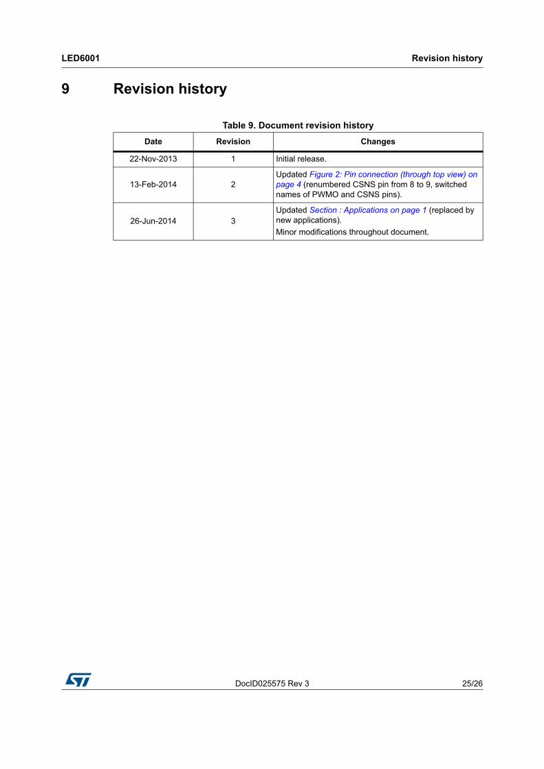
9 Revision history
Table 9. Document revision history
Date Revision Changes
22-Nov-2013 1 Initial release.
13-Feb-2014 2Updated Figure 2: Pin connection (through top view) on page 4 (renumbered CSNS pin from 8 to 9, switched names of PWMO and CSNS pins).
26-Jun-2014 3Updated Section : Applications on page 1 (replaced by new applications).
Minor modifications throughout document.

LED6001
26/26 DocID025575 Rev 3
Please Read Carefully:
Information in this document is provided solely in connection with ST products. STMicroelectronics NV and its subsidiaries (“ST”) reserve theright to make changes, corrections, modifications or improvements, to this document, and the products and services described herein at anytime, without notice.
All ST products are sold pursuant to ST’s terms and conditions of sale.
Purchasers are solely responsible for the choice, selection and use of the ST products and services described herein, and ST assumes noliability whatsoever relating to the choice, selection or use of the ST products and services described herein.
No license, express or implied, by estoppel or otherwise, to any intellectual property rights is granted under this document. If any part of thisdocument refers to any third party products or services it shall not be deemed a license grant by ST for the use of such third party productsor services, or any intellectual property contained therein or considered as a warranty covering the use in any manner whatsoever of suchthird party products or services or any intellectual property contained therein.
UNLESS OTHERWISE SET FORTH IN ST’S TERMS AND CONDITIONS OF SALE ST DISCLAIMS ANY EXPRESS OR IMPLIEDWARRANTY WITH RESPECT TO THE USE AND/OR SALE OF ST PRODUCTS INCLUDING WITHOUT LIMITATION IMPLIEDWARRANTIES OF MERCHANTABILITY, FITNESS FOR A PARTICULAR PURPOSE (AND THEIR EQUIVALENTS UNDER THE LAWSOF ANY JURISDICTION), OR INFRINGEMENT OF ANY PATENT, COPYRIGHT OR OTHER INTELLECTUAL PROPERTY RIGHT.
ST PRODUCTS ARE NOT DESIGNED OR AUTHORIZED FOR USE IN: (A) SAFETY CRITICAL APPLICATIONS SUCH AS LIFESUPPORTING, ACTIVE IMPLANTED DEVICES OR SYSTEMS WITH PRODUCT FUNCTIONAL SAFETY REQUIREMENTS; (B)AERONAUTIC APPLICATIONS; (C) AUTOMOTIVE APPLICATIONS OR ENVIRONMENTS, AND/OR (D) AEROSPACE APPLICATIONSOR ENVIRONMENTS. WHERE ST PRODUCTS ARE NOT DESIGNED FOR SUCH USE, THE PURCHASER SHALL USE PRODUCTS ATPURCHASER’S SOLE RISK, EVEN IF ST HAS BEEN INFORMED IN WRITING OF SUCH USAGE, UNLESS A PRODUCT ISEXPRESSLY DESIGNATED BY ST AS BEING INTENDED FOR “AUTOMOTIVE, AUTOMOTIVE SAFETY OR MEDICAL” INDUSTRYDOMAINS ACCORDING TO ST PRODUCT DESIGN SPECIFICATIONS. PRODUCTS FORMALLY ESCC, QML OR JAN QUALIFIED AREDEEMED SUITABLE FOR USE IN AEROSPACE BY THE CORRESPONDING GOVERNMENTAL AGENCY.
Resale of ST products with provisions different from the statements and/or technical features set forth in this document shall immediately voidany warranty granted by ST for the ST product or service described herein and shall not create or extend in any manner whatsoever, anyliability of ST.
ST and the ST logo are trademarks or registered trademarks of ST in various countries.Information in this document supersedes and replaces all information previously supplied.
The ST logo is a registered trademark of STMicroelectronics. All other names are the property of their respective owners.
© 2014 STMicroelectronics - All rights reserved
STMicroelectronics group of companies
Australia - Belgium - Brazil - Canada - China - Czech Republic - Finland - France - Germany - Hong Kong - India - Israel - Italy - Japan - Malaysia - Malta - Morocco - Philippines - Singapore - Spain - Sweden - Switzerland - United Kingdom - United States of America
www.st.com